0.4-ghzto 4-ghzquadrature modulator
TRANSCRIPT
GND
RF_OUT
15
14
13
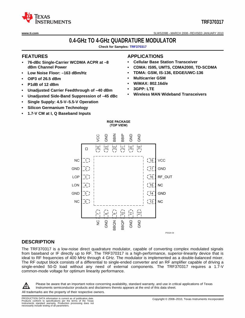
RGE PACKAGE(TOP VIEW)
VC
C
GN
D
BB
IN
BB
IP
GN
D
GN
D
24
23
22
21
20
19
GND
1
2
3LOP
4LON
5GND
GN
D
7 8 9B
BQ
N
10 11
BB
QP
GN
D
12
GN
D
18 VCC
17 GND
16
NC
NC
NC
NC
NC
P0024-04
6
TRF370317
www.ti.com SLWS209B –MARCH 2008–REVISED JANUARY 2010
0.4-GHz TO 4-GHz QUADRATURE MODULATORCheck for Samples: TRF370317
1FEATURES APPLICATIONS• Cellular Base Station Transceiver
2• 76-dBc Single-Carrier WCDMA ACPR at –8dBm Channel Power • CDMA: IS95, UMTS, CDMA2000, TD-SCDMA
• TDMA: GSM, IS-136, EDGE/UWC-136• Low Noise Floor: –163 dBm/Hz• Multicarrier GSM• OIP3 of 26.5 dBm• WiMAX: 802.16d/e• P1dB of 12 dBm• 3GPP: LTE• Unadjusted Carrier Feedthrough of –40 dBm• Wireless MAN Wideband Transceivers• Unadjusted Side-Band Suppression of –45 dBc
• Single Supply: 4.5-V–5.5-V Operation• Silicon Germanium Technology• 1.7-V CM at I, Q Baseband Inputs
DESCRIPTIONThe TRF370317 is a low-noise direct quadrature modulator, capable of converting complex modulated signalsfrom baseband or IF directly up to RF. The TRF370317 is a high-performance, superior-linearity device that isideal to RF frequencies of 400 MHz through 4 GHz. The modulator is implemented as a double-balanced mixer.The RF output block consists of a differential to single-ended converter and an RF amplifier capable of driving asingle-ended 50-Ω load without any need of external components. The TRF370317 requires a 1.7-Vcommon-mode voltage for optimum linearity performance.
1
Please be aware that an important notice concerning availability, standard warranty, and use in critical applications of TexasInstruments semiconductor products and disclaimers thereto appears at the end of this data sheet.
2All trademarks are the property of their respective owners.
PRODUCTION DATA information is current as of publication date. Copyright © 2008–2010, Texas Instruments IncorporatedProducts conform to specifications per the terms of the TexasInstruments standard warranty. Production processing does notnecessarily include testing of all parameters.

VC
C24
GN
D23
BB
IN22
BB
IP21
GN
D20
GN
D20
GN
D19
VCC18
GND17
RF_OUT16
15
14 GND
13
GN
D87
BB
QN
9
BB
QP
10
GN
D11
GN
D12
1
2GND
3LOP
4LON
GND 5
6
0/90
S
NC
NC
B0175-01
NC
NC
NC
TRF370317
SLWS209B –MARCH 2008–REVISED JANUARY 2010 www.ti.com
This integrated circuit can be damaged by ESD. Texas Instruments recommends that all integrated circuits be handled withappropriate precautions. Failure to observe proper handling and installation procedures can cause damage.
ESD damage can range from subtle performance degradation to complete device failure. Precision integrated circuits may be moresusceptible to damage because very small parametric changes could cause the device not to meet its published specifications.
Functional Block Diagram
NOTE: NC = No connection
2 Submit Documentation Feedback Copyright © 2008–2010, Texas Instruments Incorporated
Product Folder Link(s): TRF370317

TRF370317
www.ti.com SLWS209B –MARCH 2008–REVISED JANUARY 2010
DEVICE INFORMATION
TERMINAL FUNCTIONSTERMINAL
I/O DESCRIPTIONNAME NO.
BBIN 22 I In-phase negative input
BBIP 21 I In-phase positive input
BBQN 9 I Quadrature-phase negative input
BBQP 10 I Quadrature-phase positive input
2, 5, 8,11,GND 12, 14, 17, – Ground
19, 20, 23
LON 4 I Local oscillator negative input
LOP 3 I Local oscillator positive input
1, 6, 7, 13,NC – No connect15
RF_OUT 16 O RF output
VCC 18, 24 – Power supply
ABSOLUTE MAXIMUM RATINGS (1)
over operating free-air temperature range (unless otherwise noted)
VALUE (2) UNIT
Supply voltage range –0.3 V to 6 V
TJ Operating virtual junction temperature range –40 to 150 °C
TA Operating ambient temperature range –40 to 85 °C
Tstg Storage temperature range –65 to 150 °C
Human body model (HBM) 75 VESD Electrostatic discharge ratings
Charged device model (CDM) 75 V
(1) Stresses beyond those listed under Absolute Maximum Ratings may cause permanent damage to the device. These are stress ratingsonly, and functional operation of the device at these or any other conditions beyond those indicated under Recommended OperatingConditions is not implied. Exposure to absolute-maximum-rated conditions for extended periods may affect device reliability.
(2) All voltage values are with respect to network ground terminal.
RECOMMENDED OPERATING CONDITIONSover operating free-air temperature range (unless otherwise noted)
MIN NOM MAX UNIT
VCC Power-supply voltage 4.5 5 5.5 V
THERMAL CHARACTERISTICSPARAMETER TEST CONDITIONS VALUE UNIT
RqJA Thermal resistance, junction-to-ambient High-K board, still air 29.4 °C/W
RqJC Thermal resistance, junction-to-case 18.6 °C/W
Copyright © 2008–2010, Texas Instruments Incorporated Submit Documentation Feedback 3
Product Folder Link(s): TRF370317

TRF370317
SLWS209B –MARCH 2008–REVISED JANUARY 2010 www.ti.com
ELECTRICAL CHARACTERISTICSover operating free-air temperature range (unless otherwise noted)
PARAMETER TEST CONDITIONS MIN TYP MAX UNIT
DC Parameters
ICC Total supply current (1.7 V CM) TA = 25°C 205 245 mA
LO Input (50-Ω, Single-Ended)
LO frequency range 0.4 4 GHz
fLO LO input power –5 0 12 dBm
LO port return loss 15 dB
Baseband Inputs
VCM I and Q input dc common voltage 1.7
BW 1-dB input frequency bandwidth 350 MHz
Input impedance, resistance 5 kΩZI(single
Input impedance, parallelended) 3 pFcapacitance
ELECTRICAL CHARACTERISTICSover recommended operating conditions, power supply = 5 V, TA = 25°C, VCM = 1.7 V, fLO = 400 MHz at 8 dBm, VinBB = 98mVrms single-ended in quadrature, fBB = 50 kHz (unless otherwise noted)
RF Output Parameters
PARAMETER TEST CONDITIONS MIN TYP MAX UNIT
G Voltage gain Output rms voltage over input I (or Q) rms voltage –1.9 dB
P1dB Output compression point 11 dBm
IP3 Output IP3 fBB = 4.5, 5.5 MHz 24.5 dBm
IP2 Output IP2 fBB = 4.5, 5.5 MHz 68 dBm
Carrier feedthrough Unadjusted –38 dBm
Sideband suppression Unadjusted –40 dBc
4 Submit Documentation Feedback Copyright © 2008–2010, Texas Instruments Incorporated
Product Folder Link(s): TRF370317
TRF370317
www.ti.com SLWS209B –MARCH 2008–REVISED JANUARY 2010
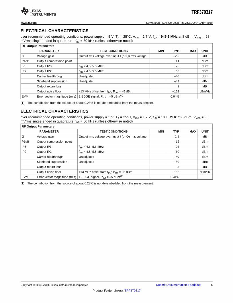
ELECTRICAL CHARACTERISTICSover recommended operating conditions, power supply = 5 V, TA = 25°C, VCM = 1.7 V, fLO = 945.6 MHz at 8 dBm, VinBB = 98mVrms single-ended in quadrature, fBB = 50 kHz (unless otherwise noted)
RF Output Parameters
PARAMETER TEST CONDITIONS MIN TYP MAX UNIT
G Voltage gain Output rms voltage over input I (or Q) rms voltage –2.5 dB
P1dB Output compression point 11 dBm
IP3 Output IP3 fBB = 4.5, 5.5 MHz 25 dBm
IP2 Output IP2 fBB = 4.5, 5.5 MHz 65 dBm
Carrier feedthrough Unadjusted –40 dBm
Sideband suppression Unadjusted –42 dBc
Output return loss 9 dB
Output noise floor ≥13 MHz offset from fLO; Pout = –5 dBm –163 dBm/Hz
EVM Error vector magnitude (rms) 1 EDGE signal, Pout = –5 dBm (1) 0.64%
(1) The contribution from the source of about 0.28% is not de-embedded from the measurement.
ELECTRICAL CHARACTERISTICSover recommended operating conditions, power supply = 5 V, TA = 25°C, VCM = 1.7 V, fLO = 1800 MHz at 8 dBm, VinBB = 98mVrms single-ended in quadrature, fBB = 50 kHz (unless otherwise noted)
RF Output Parameters
PARAMETER TEST CONDITIONS MIN TYP MAX UNIT
G Voltage gain Output rms voltage over input I (or Q) rms voltage –2.5 dB
P1dB Output compression point 12 dBm
IP3 Output IP3 fBB = 4.5, 5.5 MHz 26 dBm
IP2 Output IP2 fBB = 4.5, 5.5 MHz 60 dBm
Carrier feedthrough Unadjusted –40 dBm
Sideband suppression Unadjusted –50 dBc
Output return loss 8 dB
Output noise floor ≥13 MHz offset from fLO; Pout = –5 dBm –162 dBm/Hz
EVM Error vector magnitude (rms) 1 EDGE signal, Pout = –5 dBm (1) 0.41%
(1) The contribution from the source of about 0.28% is not de-embedded from the measurement.
Copyright © 2008–2010, Texas Instruments Incorporated Submit Documentation Feedback 5
Product Folder Link(s): TRF370317

TRF370317
SLWS209B –MARCH 2008–REVISED JANUARY 2010 www.ti.com
ELECTRICAL CHARACTERISTICSover recommended operating conditions, power supply = 5 V, TA = 25°C, VCM = 1.7 V, fLO = 1960 MHz at 8 dBm, VinBB = 98mVrms single-ended in quadrature, fBB = 50 kHz (unless otherwise noted)
RF Output Parameters
PARAMETER TEST CONDITIONS MIN TYP MAX UNIT
G Voltage gain Output rms voltage over input I (or Q) rms voltage –2.5 dB
P1dB Output compression point 12 dBm
IP3 Output IP3 fBB = 4.5, 5.5 MHz 23.5 26.5 dBm
IP2 Output IP2 fBB = 4.5, 5.5 MHz 60 dBm
Carrier feedthrough Unadjusted –38 dBm
Sideband suppression Unadjusted –50 dBc
Output return loss 8 dB
Output noise floor ≥13 MHz offset from fLO; Pout = –5 dBm –162.5 dBm/Hz
EVM Error vector magnitude (rms) 1 EDGE signal, Pout = –5 dBm (1) 0.43%
1 WCDMA signal; Pout = –8 dBm –74Adjacent-channel powerACPR (2) 2 WCDMA signals; Pout = –11 dBm per carrier –68 dBcratio
4 WCDMA signals; Pout = –14 dBm per carrier –67
1 WCDMA signal; Pout = –8 dBm –78Alternate-channel power 2 WCDMA signals; Pout = –11 dBm per carrier –72 dBcratio
4 WCDMA signals; Pout = –14 dBm per carrier –69
(1) The contribution from the source of about 0.28% is not de-embedded from the measurement.(2) Measured with DAC5687 as source generator
ELECTRICAL CHARACTERISTICSover recommended operating conditions, power supply = 5 V, TA = 25°C, VCM = 1.7 V, fLO = 2140 MHz at 8 dBm, VinBB = 98mVrms single-ended in quadrature, fBB = 50 kHz (unless otherwise noted)
RF Output Parameters
PARAMETER TEST CONDITIONS MIN TYP MAX UNIT
G Voltage gain Output rms voltage over input I (or Q) rms voltage –2.4 dB
P1dB Output compression point 12 dBm
IP3 Output IP3 fBB = 4.5, 5.5 MHz 26.5 dBm
IP2 Output IP2 fBB = 4.5, 5.5 MHz 66 dBm
Carrier feedthrough Unadjusted –38 dBm
Sideband suppression Unadjusted –50 dBc
Output return loss 8.5 dB
Output noise floor ≥13 MHz offset from fLO ; Pout = –5 dBm –162.5 dBm/Hz
1 WCDMA signal; Pout = –8 dBm –72Adjacent-channel powerACPR (1) 2 WCDMA signal; Pout = –11 dBm per carrier –67 dBcratio
4 WCDMA signals; Pout = –14 dBm per carrier –66
1 WCDMA signal; Pout = –8 dBm –78Alternate-channel power 2 WCDMA signal; Pout = –11 dBm –74 dBcratio
4 WCDMA signals; Pout = –14 dBm per carrier –68
(1) Measured with DAC5687 as source generator
6 Submit Documentation Feedback Copyright © 2008–2010, Texas Instruments Incorporated
Product Folder Link(s): TRF370317
TRF370317
www.ti.com SLWS209B –MARCH 2008–REVISED JANUARY 2010
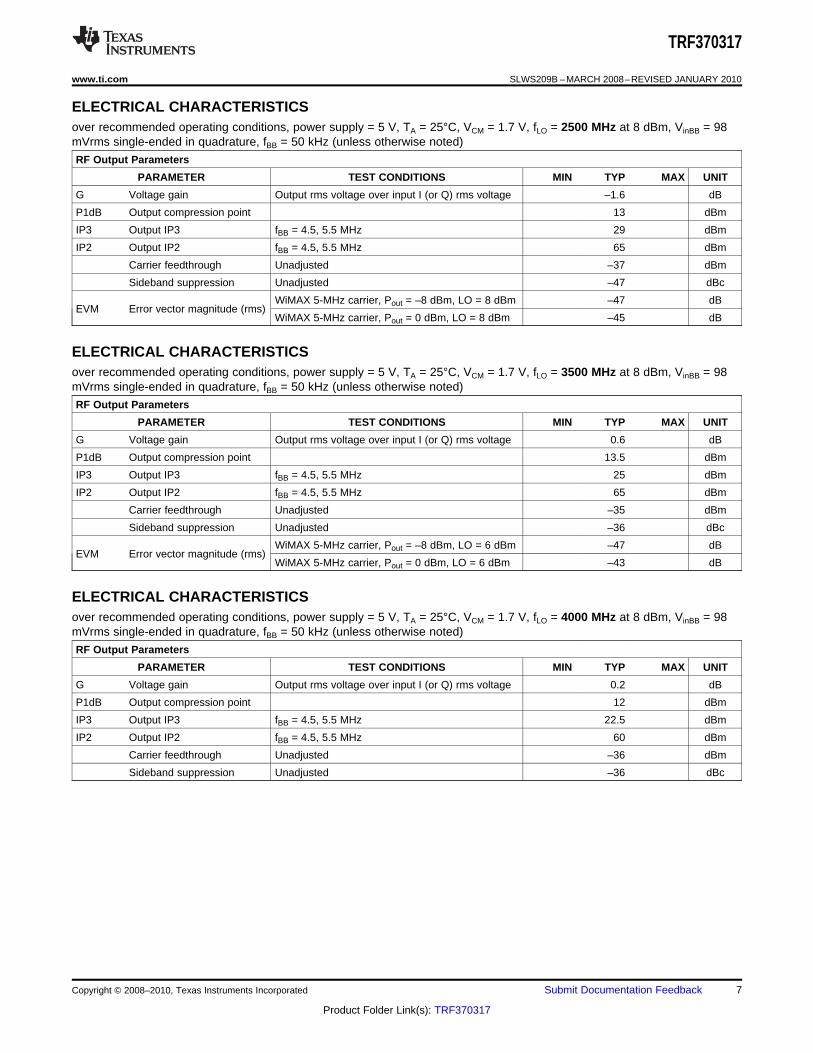
ELECTRICAL CHARACTERISTICSover recommended operating conditions, power supply = 5 V, TA = 25°C, VCM = 1.7 V, fLO = 2500 MHz at 8 dBm, VinBB = 98mVrms single-ended in quadrature, fBB = 50 kHz (unless otherwise noted)
RF Output Parameters
PARAMETER TEST CONDITIONS MIN TYP MAX UNIT
G Voltage gain Output rms voltage over input I (or Q) rms voltage –1.6 dB
P1dB Output compression point 13 dBm
IP3 Output IP3 fBB = 4.5, 5.5 MHz 29 dBm
IP2 Output IP2 fBB = 4.5, 5.5 MHz 65 dBm
Carrier feedthrough Unadjusted –37 dBm
Sideband suppression Unadjusted –47 dBc
WiMAX 5-MHz carrier, Pout = –8 dBm, LO = 8 dBm –47 dBEVM Error vector magnitude (rms)
WiMAX 5-MHz carrier, Pout = 0 dBm, LO = 8 dBm –45 dB
ELECTRICAL CHARACTERISTICSover recommended operating conditions, power supply = 5 V, TA = 25°C, VCM = 1.7 V, fLO = 3500 MHz at 8 dBm, VinBB = 98mVrms single-ended in quadrature, fBB = 50 kHz (unless otherwise noted)
RF Output Parameters
PARAMETER TEST CONDITIONS MIN TYP MAX UNIT
G Voltage gain Output rms voltage over input I (or Q) rms voltage 0.6 dB
P1dB Output compression point 13.5 dBm
IP3 Output IP3 fBB = 4.5, 5.5 MHz 25 dBm
IP2 Output IP2 fBB = 4.5, 5.5 MHz 65 dBm
Carrier feedthrough Unadjusted –35 dBm
Sideband suppression Unadjusted –36 dBc
WiMAX 5-MHz carrier, Pout = –8 dBm, LO = 6 dBm –47 dBEVM Error vector magnitude (rms)
WiMAX 5-MHz carrier, Pout = 0 dBm, LO = 6 dBm –43 dB
ELECTRICAL CHARACTERISTICSover recommended operating conditions, power supply = 5 V, TA = 25°C, VCM = 1.7 V, fLO = 4000 MHz at 8 dBm, VinBB = 98mVrms single-ended in quadrature, fBB = 50 kHz (unless otherwise noted)
RF Output Parameters
PARAMETER TEST CONDITIONS MIN TYP MAX UNIT
G Voltage gain Output rms voltage over input I (or Q) rms voltage 0.2 dB
P1dB Output compression point 12 dBm
IP3 Output IP3 fBB = 4.5, 5.5 MHz 22.5 dBm
IP2 Output IP2 fBB = 4.5, 5.5 MHz 60 dBm
Carrier feedthrough Unadjusted –36 dBm
Sideband suppression Unadjusted –36 dBc
Copyright © 2008–2010, Texas Instruments Incorporated Submit Documentation Feedback 7
Product Folder Link(s): TRF370317

f − Frequency − MHz
−10
−9
−8
−7
−6
−5
−4
−3
−2
−1
0
0 500 1000 1500 2000 2500 3000 3500 4000 4500
PO
UT −
Out
put P
ower
− d
Bm
G002
–40°C
25°C
85°C
VIN = 98 mVrms SELO = 8 dBmVCC = 5 V
−20
−15
−10
−5
0
5
10
15
VBB − Baseband Voltage Single-Ended RMS − V
PO
UT −
Out
put P
ower
at 2
.14
GH
z −
dBm
0.01 0.1 1
G001
f − Frequency − MHz
−10
−9
−8
−7
−6
−5
−4
−3
−2
−1
0
0 500 1000 1500 2000 2500 3000 3500 4000 4500
PO
UT −
Out
put P
ower
− d
Bm
G003
VIN = 98 mVrms SELO = 8 dBmTA = 25°C
4.5 V
5 V
5.5 V
f − Frequency − MHz
−10
−9
−8
−7
−6
−5
−4
−3
−2
−1
0
0 500 1000 1500 2000 2500 3000 3500 4000 4500
PO
UT −
Out
put P
ower
− d
Bm
G004
VIN = 98 mVrms SEVCC = 5 VTA = 25°C
–5 dBm
8 dBm
0 dBm
TRF370317
SLWS209B –MARCH 2008–REVISED JANUARY 2010 www.ti.com
TYPICAL CHARACTERISTICSVCM = 1.7 V, VinBB = 98 mVrms single-ended sine wave in quadrature, VCC = 5 V, LO power = 8 dBm (single-ended), fBB = 50
kHz (unless otherwise noted).
OUTPUT POWER OUTPUT POWERvs vs
BASEBAND VOLTAGE FREQUENCY AND TEMPERATURE
Figure 1. Figure 2.
OUTPUT POWER OUTPUT POWERvs vs
FREQUENCY AND SUPPLY VOLTAGE FREQUENCY AND LO POWER
Figure 3. Figure 4.
8 Submit Documentation Feedback Copyright © 2008–2010, Texas Instruments Incorporated
Product Folder Link(s): TRF370317

f − Frequency − MHz
0
2
4
6
8
10
12
14
16
0 500 1000 1500 2000 2500 3000 3500 4000 4500
P1d
B −
dB
m
G005
85°C–40°C25°C
LO = 8 dBmVCC = 5 V
f − Frequency − MHz
0
2
4
6
8
10
12
14
16
0 500 1000 1500 2000 2500 3000 3500 4000 4500
P1d
B −
dB
m
G006
4.5 V
LO = 8 dBmTA = 25°C
5.5 V
5 V
f − Frequency − MHz
0
5
10
15
20
25
30
35
40
0 500 1000 1500 2000 2500 3000 3500 4000 4500
OIP
3 −
dBm
G008
fBB = 4.5, 5.5 MHzLO = 8 dBmVCC = 5 V
–40°C25°C
85°C
f − Frequency − MHz
0
2
4
6
8
10
12
14
16
0 500 1000 1500 2000 2500 3000 3500 4000 4500
P1d
B −
dB
m
G007
–5 dBm
VCC = 5 VTA = 25°C
0 dBm
8 dBm
TRF370317
www.ti.com SLWS209B –MARCH 2008–REVISED JANUARY 2010
TYPICAL CHARACTERISTICS (continued)
VCM = 1.7 V, VinBB = 98 mVrms single-ended sine wave in quadrature, VCC = 5 V, LO power = 8 dBm (single-ended), fBB = 50kHz (unless otherwise noted).
P1dB P1dBvs vs
FREQUENCY AND TEMPERATURE FREQUENCY AND SUPPLY VOLTAGE
Figure 5. Figure 6.
P1dB OIP3vs vs
FREQUENCY AND LO POWER FREQUENCY AND TEMPERATURE
Figure 7. Figure 8.
Copyright © 2008–2010, Texas Instruments Incorporated Submit Documentation Feedback 9
Product Folder Link(s): TRF370317

f − Frequency − MHz
0
5
10
15
20
25
30
35
0 500 1000 1500 2000 2500 3000 3500 4000 4500
OIP
3 −
dBm
G009
5 V
fBB = 4.5, 5.5 MHzLO = 8 dBmTA = 25°C
4.5 V 5.5 V
0
5
10
15
20
25
30
35
0 500 1000 1500 2000 2500 3000 3500 4000 4500
f − Frequency − MHz
OIP
3 −
dBm
G010
–5 dBm
fBB = 4.5, 5.5 MHzVCC = 5 VTA = 25°C
0 dBm
8 dBm
f − Frequency − MHz
0
10
20
30
40
50
60
70
80
90
100
0 500 1000 1500 2000 2500 3000 3500 4000 4500
OIP
2 −
dBm
G011
fBB = 4.5, 5.5 MHzLO = 8 dBmVCC = 5 V
–40°C
25°C
85°C
f − Frequency − MHz
0
10
20
30
40
50
60
70
80
90
100
0 500 1000 1500 2000 2500 3000 3500 4000 4500
OIP
2 −
dBm
G012
fBB = 4.5, 5.5 MHzLO = 8 dBmTA = 25°C
4.5 V
5.5 V
5 V
TRF370317
SLWS209B –MARCH 2008–REVISED JANUARY 2010 www.ti.com
TYPICAL CHARACTERISTICS (continued)
VCM = 1.7 V, VinBB = 98 mVrms single-ended sine wave in quadrature, VCC = 5 V, LO power = 8 dBm (single-ended), fBB = 50kHz (unless otherwise noted).
OIP3 OIP3vs vs
FREQUENCY AND SUPPLY VOLTAGE FREQUENCY AND LO POWER
Figure 9. Figure 10.
OIP2 OIP2vs vs
FREQUENCY AND TEMPERATURE FREQUENCY AND SUPPLY VOLTAGE
Figure 11. Figure 12.
10 Submit Documentation Feedback Copyright © 2008–2010, Texas Instruments Incorporated
Product Folder Link(s): TRF370317
0
10
20
30
40
50
60
70
80
90
100
0 500 1000 1500 2000 2500 3000 3500 4000 4500
f − Frequency − MHz
OIP
2 −
dBm
G013
fBB = 4.5, 5.5 MHzVCC = 5 VTA = 25°C
0 dBm
8 dBm
–5 dBm
f − Frequency − MHz
−60
−50
−40
−30
−20
−10
0
0 500 1000 1500 2000 2500 3000 3500 4000 4500
CS
− U
nadj
uste
d C
arrie
r F
eedt
hrou
gh −
dB
m
G014
LO = 8 dBmVCC = 5 V
–40°C
25°C
85°C
f − Frequency − MHz
−60
−50
−40
−30
−20
−10
0
0 500 1000 1500 2000 2500 3000 3500 4000 4500
CS
− U
nadj
uste
d C
arrie
r F
eedt
hrou
gh −
dB
m
G016
VCC = 5 VTA = 25°C
–5 dBm
0 dBm
8 dBm
f − Frequency − MHz
−60
−50
−40
−30
−20
−10
0
0 500 1000 1500 2000 2500 3000 3500 4000 4500
CS
− U
nadj
uste
d C
arrie
r F
eedt
hrou
gh −
dB
m
G015
LO = 8 dBmTA = 25°C
5.5 V
5 V4.5 V
TRF370317
www.ti.com SLWS209B –MARCH 2008–REVISED JANUARY 2010
TYPICAL CHARACTERISTICS (continued)
VCM = 1.7 V, VinBB = 98 mVrms single-ended sine wave in quadrature, VCC = 5 V, LO power = 8 dBm (single-ended), fBB = 50kHz (unless otherwise noted).
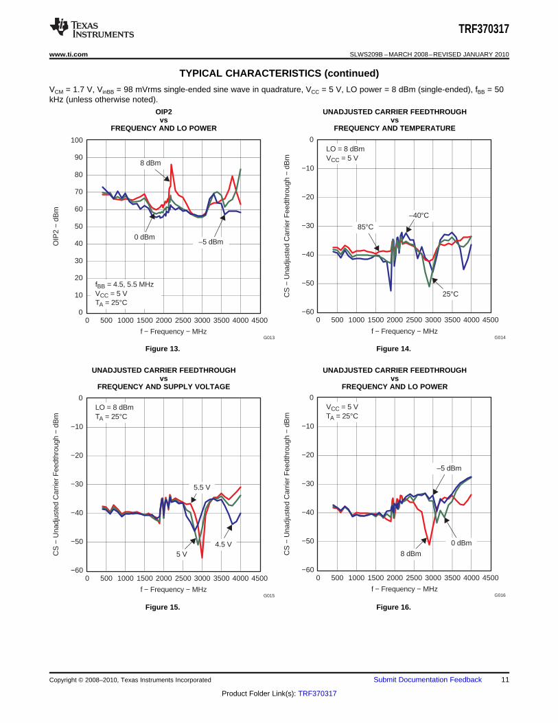
OIP2 UNADJUSTED CARRIER FEEDTHROUGHvs vs
FREQUENCY AND LO POWER FREQUENCY AND TEMPERATURE
Figure 13. Figure 14.
UNADJUSTED CARRIER FEEDTHROUGH UNADJUSTED CARRIER FEEDTHROUGHvs vs
FREQUENCY AND SUPPLY VOLTAGE FREQUENCY AND LO POWER
Figure 15. Figure 16.
Copyright © 2008–2010, Texas Instruments Incorporated Submit Documentation Feedback 11
Product Folder Link(s): TRF370317

f − Frequency − MHz
−80
−70
−60
−50
−40
−30
−20
−10
0
0 500 1000 1500 2000 2500 3000 3500 4000 4500
SS
− U
nadj
uste
d S
ideb
and
Sup
pres
sion
− d
Bc
G017
LO = 8 dBmPOUT = −3 dBmVCC = 5 V
85°C
25°C
–40°C
f − Frequency − MHz
−80
−70
−60
−50
−40
−30
−20
−10
0
0 500 1000 1500 2000 2500 3000 3500 4000 4500
SS
− U
nadj
uste
d S
ideb
and
Sup
pres
sion
− d
Bc
G018
LO = 8 dBmPOUT = −3 dBmTA = 25°C
5.5 V
5 V
4.5 V
f − Frequency − MHz
−80
−70
−60
−50
−40
−30
−20
−10
0
0 500 1000 1500 2000 2500 3000 3500 4000 4500
SS
− U
nadj
uste
d S
ideb
and
Sup
pres
sion
− d
Bc
G019
VCC = 5 VPOUT = −3 dBmTA = 25°C
–5 dBm
0 dBm
8 dBm
f − Frequency − GHz
−170
−168
−166
−164
−162
−160
−158
−156
−154
−152
−150
0.8 1.2 1.6 2.0 2.4 2.8 3.2 3.6 4.0
Noi
se a
t 13-
MH
z O
ffset
− d
Bm
/Hz
G020
85°C
–40°C
25°C
VCC = 5 VLO = 8 dBmPOUT = −5 dBm
TRF370317
SLWS209B –MARCH 2008–REVISED JANUARY 2010 www.ti.com
TYPICAL CHARACTERISTICS (continued)
VCM = 1.7 V, VinBB = 98 mVrms single-ended sine wave in quadrature, VCC = 5 V, LO power = 8 dBm (single-ended), fBB = 50kHz (unless otherwise noted).
UNADJUSTED SIDEBAND SUPPRESSION UNADJUSTED SIDEBAND SUPPRESSIONvs vs
FREQUENCY AND TEMPERATURE FREQUENCY AND SUPPLY VOLTAGE
Figure 17. Figure 18.
UNADJUSTED SIDEBAND SUPPRESSION NOISE AT 13-MHz OFFSET (dBm/Hz)vs vs
FREQUENCY AND LO POWER FREQUENCY AND TEMPERATURE
Figure 19. Figure 20.
12 Submit Documentation Feedback Copyright © 2008–2010, Texas Instruments Incorporated
Product Folder Link(s): TRF370317

POUT − Output Power − dBm
−170
−168
−166
−164
−162
−160
−158
−156
−154
−152
−150
−10−9 −8 −7 −6 −5 −4 −3 −2 −1 0 1 2 3 4 5
Noi
se a
t 13-
MH
z O
ffset
− d
Bm
/Hz
G022
1960 MHz
LO = 8 dBmVCC = 5 V TA = 25°C
2140 MHz
f − Frequency − GHz
−170
−168
−166
−164
−162
−160
−158
−156
−154
−152
−150
0.8 1.2 1.6 2.0 2.4 2.8 3.2 3.6 4.0
Noi
se a
t 13-
MH
z O
ffset
− d
Bm
/Hz
G021
5.5 V
5 V
LO = 8 dBmPOUT = −5 dBmTA = 25°C
4.5 V
−100
−90
−80
−70
−60
−50
−40
−30
−20
−10
0
900 920 940 960 980 1000
f − Frequency − MHz
CS
− A
djus
ted
Car
rier
Fee
dthr
ough
− d
Bm
G023
85°C
Adj at 942.6 MHzLO = 8 dBmVCC = 5 V
–40°C
25°C
−100
−90
−80
−70
−60
−50
−40
−30
−20
−10
0
1910 1930 1950 1970 1990 2010
f − Frequency − MHz
CS
− A
djus
ted
Car
rier
Fee
dthr
ough
− d
Bm
G024
85°C
Adj at 1960 MHzLO = 8 dBmVCC = 5 V
–40°C
25°C
TRF370317
www.ti.com SLWS209B –MARCH 2008–REVISED JANUARY 2010
TYPICAL CHARACTERISTICS (continued)
VCM = 1.7 V, VinBB = 98 mVrms single-ended sine wave in quadrature, VCC = 5 V, LO power = 8 dBm (single-ended), fBB = 50kHz (unless otherwise noted).
NOISE AT 13-MHz OFFSET (dBm/Hz) NOISE AT 13-MHz OFFSET (dBm/Hz)vs vs
FREQUENCY AND SUPPLY VOLTAGE OUTPUT POWER
Figure 21. Figure 22.
ADJUSTED CARRIER FEEDTHROUGH ADJUSTED CARRIER FEEDTHROUGHvs vs
FREQUENCY AND TEMPERATURE FREQUENCY AND TEMPERATURE
Figure 23. Figure 24.
Copyright © 2008–2010, Texas Instruments Incorporated Submit Documentation Feedback 13
Product Folder Link(s): TRF370317

−100
−90
−80
−70
−60
−50
−40
−30
−20
−10
0
2400 2440 2480 2520 2560 2600
f − Frequency − MHz
CS
− A
djus
ted
Car
rier
Fee
dthr
ough
− d
Bm
G026
85°C
Adj at 2500 MHzLO = 8 dBmVCC = 5 V
–40°C
25°C
−100
−90
−80
−70
−60
−50
−40
−30
−20
−10
0
2090 2110 2130 2150 2170 2190
f − Frequency − MHz
CS
− A
djus
ted
Car
rier
Fee
dthr
ough
− d
Bm
G025
85°C
Adj at 2140 MHzLO = 8 dBmVCC = 5 V
–40°C
25°C
−100
−90
−80
−70
−60
−50
−40
−30
−20
−10
0
3400 3440 3480 3520 3560 3600
f − Frequency − MHz
CS
− A
djus
ted
Car
rier
Fee
dthr
ough
− d
Bm
G027
85°C
Adj at 3500 MHzLO = 8 dBmVCC = 5 V
–40°C
25°C
−80
−70
−60
−50
−40
−30
−20
−10
0
900 920 940 960 980 1000
f − Frequency − MHz
SS
− A
djus
ted
Sid
eban
d S
uppr
essi
on −
dB
c
G028
25°C
85°C
Adj at 942.6 MHzLO = 8 dBmPOUT = −3 dBmVCC = 5 V
–40°C
TRF370317
SLWS209B –MARCH 2008–REVISED JANUARY 2010 www.ti.com
TYPICAL CHARACTERISTICS (continued)
VCM = 1.7 V, VinBB = 98 mVrms single-ended sine wave in quadrature, VCC = 5 V, LO power = 8 dBm (single-ended), fBB = 50kHz (unless otherwise noted).
ADJUSTED CARRIER FEEDTHROUGH ADJUSTED CARRIER FEEDTHROUGHvs vs
FREQUENCY AND TEMPERATURE FREQUENCY AND TEMPERATURE
Figure 25. Figure 26.
ADJUSTED CARRIER FEEDTHROUGH ADJUSTED SIDEBAND SUPPRESSIONvs vs
FREQUENCY AND TEMPERATURE FREQUENCY AND TEMPERATURE
Figure 27. Figure 28.
14 Submit Documentation Feedback Copyright © 2008–2010, Texas Instruments Incorporated
Product Folder Link(s): TRF370317

−80
−70
−60
−50
−40
−30
−20
−10
0
1860 1900 1940 1980 2020 2060
f − Frequency − MHz
SS
− A
djus
ted
Sid
eban
d S
uppr
essi
on −
dB
c
G029
85°C
Adj at 1960 MHzLO = 8 dBmPOUT = −3 dBmVCC = 5 V
–40°C 25°C
−80
−70
−60
−50
−40
−30
−20
−10
0
2040 2080 2120 2160 2200 2240
f − Frequency − MHz
SS
− A
djus
ted
Sid
eban
d S
uppr
essi
on −
dB
c
G030
85°C
Adj at 2140 MHzLO = 8 dBmPOUT = −3 dBmVCC = 5 V
25°C
–40°C
−80
−70
−60
−50
−40
−30
−20
−10
0
2400 2440 2480 2520 2560 2600
f − Frequency − MHz
SS
− A
djus
ted
Sid
eban
d S
uppr
essi
on −
dB
c
G031
85°C
Adj at 2500 MHzLO = 8 dBmPOUT = −3 dBmVCC = 5 V
25°C
–40°C
−80
−70
−60
−50
−40
−30
−20
−10
0
3400 3440 3480 3520 3560 3600
f − Frequency − MHz
SS
− A
djus
ted
Sid
eban
d S
uppr
essi
on −
dB
c
G032
85°C
Adj at 3500 MHzLO = 8 dBmPOUT = −3 dBmVCC = 5 V
25°C
–40°C
TRF370317
www.ti.com SLWS209B –MARCH 2008–REVISED JANUARY 2010
TYPICAL CHARACTERISTICS (continued)
VCM = 1.7 V, VinBB = 98 mVrms single-ended sine wave in quadrature, VCC = 5 V, LO power = 8 dBm (single-ended), fBB = 50kHz (unless otherwise noted).
ADJUSTED SIDEBAND SUPPRESSION ADJUSTED SIDEBAND SUPPRESSIONvs vs
FREQUENCY AND TEMPERATURE FREQUENCY AND TEMPERATURE
Figure 29. Figure 30.
ADJUSTED SIDEBAND SUPPRESSION ADJUSTED SIDEBAND SUPPRESSIONvs vs
FREQUENCY AND TEMPERATURE FREQUENCY AND TEMPERATURE
Figure 31. Figure 32.
Copyright © 2008–2010, Texas Instruments Incorporated Submit Documentation Feedback 15
Product Folder Link(s): TRF370317

0
5
10
15
20
25
30
35
1.2 1.3 1.4 1.5 1.6 1.7 1.8 1.9
VCM − Common-Mode Voltage − V
OIP
3 −
dBm
G033
1960 MHz
LO = 8 dBmVCC = 5 V TA = 25°C
2141 MHz
0
10
20
30
40
50
60
70
80
90
1.2 1.3 1.4 1.5 1.6 1.7 1.8 1.9
VCM − Common-Mode Voltage − V
OIP
2 −
dBm
G034
1960 MHz
LO = 8 dBmVCC = 5 V TA = 25°C
2141 MHz
POUT − Output Power − dBm
−90
−87
−84
−81
−78
−75
−72
−69
−66
−63
−60
−20 −18 −16 −14 −12 −10 −8 −6 −4
AC
PR
− A
djac
ent C
hann
el P
ower
Rat
io −
dB
c
G042
ADJ
ALT
Notes: 1. Using TTE’s LE7640T-2.2M-50-720A LPF on Baseband inputs2. Using TI’s DAC5687 as a source generator
Single Carrier, 2140 MHz
POUT − Output Power − dBm
−90
−87
−84
−81
−78
−75
−72
−69
−66
−63
−60
−20 −18 −16 −14 −12 −10 −8 −6 −4
AC
PR
− A
djac
ent C
hann
el P
ower
Rat
io −
dB
c
G041
ADJ
ALT
Notes: 1. Using TTE’s LE7640T-2.2M-50-720A LPF on Baseband inputs2. Using TI’s DAC5687 as a source generator
Single Carrier, 1960 MHz
TRF370317
SLWS209B –MARCH 2008–REVISED JANUARY 2010 www.ti.com
TYPICAL CHARACTERISTICS (continued)
VCM = 1.7 V, VinBB = 98 mVrms single-ended sine wave in quadrature, VCC = 5 V, LO power = 8 dBm (single-ended), fBB = 50kHz (unless otherwise noted).
OIP3 OIP2vs vs
COMMON-MODE VOLTAGE COMMON-MODE VOLTAGE
Figure 33. Figure 34.
ADJACENT CHANNEL POWER RATIO ADJACENT CHANNEL POWER RATIOvs vs
OUTPUT POWER OUTPUT POWER
Figure 35. Figure 36.
16 Submit Documentation Feedback Copyright © 2008–2010, Texas Instruments Incorporated
Product Folder Link(s): TRF370317
OIP2 − dBm
0
5
10
15
20
25
56 58 60 62 64 66 68 70 72
Dis
trib
utio
n −
%
G037OIP3 − dBm
0
10
20
30
40
50
60
24 25 26 27 28 29
Dis
trib
utio
n −
%
G036
SS − Unadjusted Sideband Suppression − dBc
0
5
10
15
20
25
30
−36 −40 −44 −48 −52 −56 −60 −64 −68 −72 −76
Dis
trib
utio
n −
%
G039CS − Unadjusted Carrier Feedthrough − dBm
0
2
4
6
8
10
12
14
16
18
−24 −28 −32 −36 −40 −44 −48 −52 −56 −60 −64
Dis
trib
utio
n −
%
G038
TRF370317
www.ti.com SLWS209B –MARCH 2008–REVISED JANUARY 2010
TYPICAL CHARACTERISTICS (continued)
VCM = 1.7 V, VinBB = 98 mVrms single-ended sine wave in quadrature, VCC = 5 V, LO power = 8 dBm (single-ended), fBB = 50kHz (unless otherwise noted).
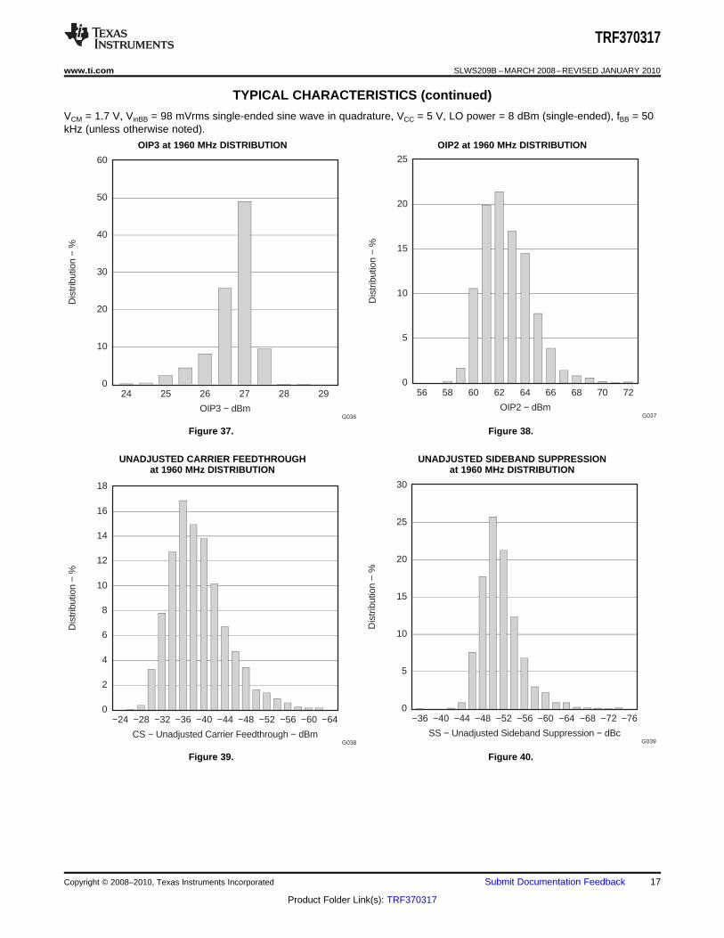
OIP3 at 1960 MHz DISTRIBUTION OIP2 at 1960 MHz DISTRIBUTION
Figure 37. Figure 38.
UNADJUSTED CARRIER FEEDTHROUGH UNADJUSTED SIDEBAND SUPPRESSIONat 1960 MHz DISTRIBUTION at 1960 MHz DISTRIBUTION
Figure 39. Figure 40.
Copyright © 2008–2010, Texas Instruments Incorporated Submit Documentation Feedback 17
Product Folder Link(s): TRF370317
P1dB − dBm
0
5
10
15
20
25
30
35
11.4 11.6 11.8 12 12.2 12.4
Dis
trib
utio
n −
%
G040
TRF370317
SLWS209B –MARCH 2008–REVISED JANUARY 2010 www.ti.com
TYPICAL CHARACTERISTICS (continued)
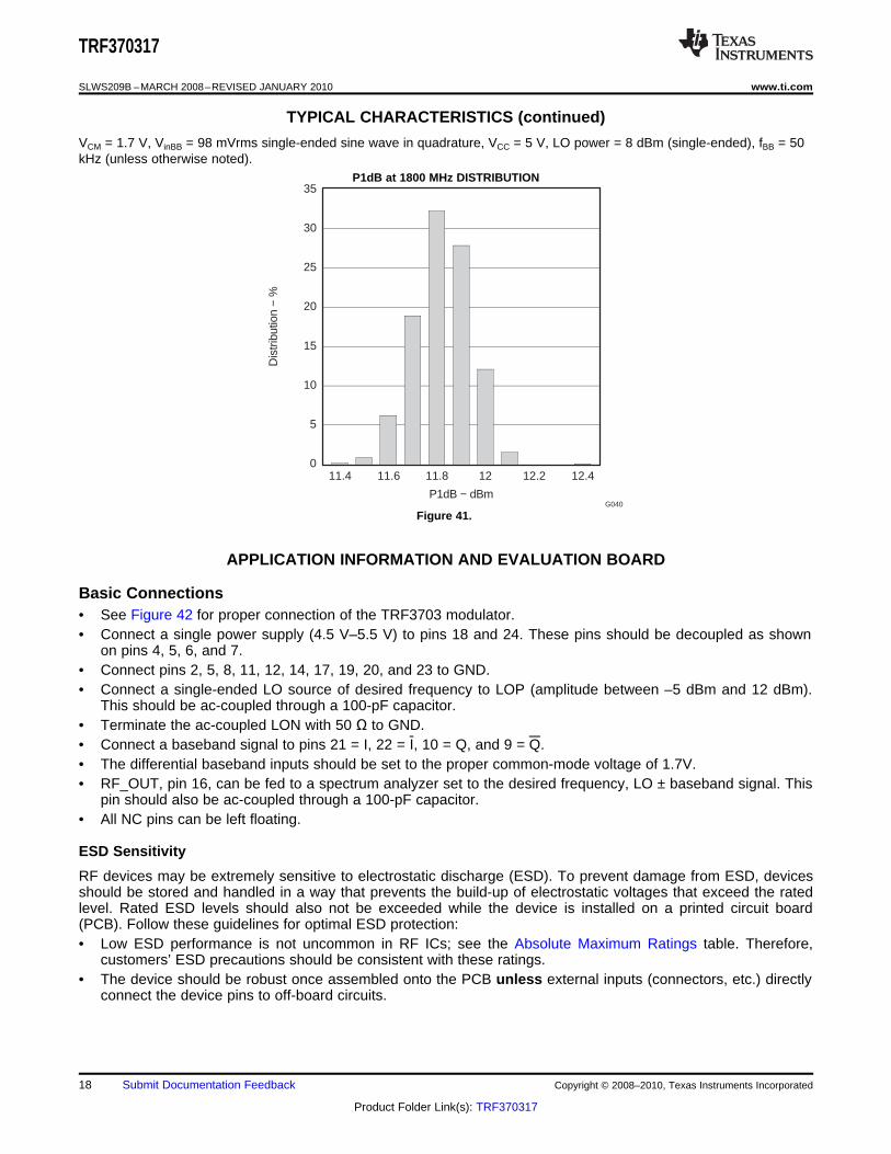
VCM = 1.7 V, VinBB = 98 mVrms single-ended sine wave in quadrature, VCC = 5 V, LO power = 8 dBm (single-ended), fBB = 50kHz (unless otherwise noted).
P1dB at 1800 MHz DISTRIBUTION
Figure 41.
APPLICATION INFORMATION AND EVALUATION BOARD
Basic Connections• See Figure 42 for proper connection of the TRF3703 modulator.• Connect a single power supply (4.5 V–5.5 V) to pins 18 and 24. These pins should be decoupled as shown
on pins 4, 5, 6, and 7.• Connect pins 2, 5, 8, 11, 12, 14, 17, 19, 20, and 23 to GND.• Connect a single-ended LO source of desired frequency to LOP (amplitude between –5 dBm and 12 dBm).
This should be ac-coupled through a 100-pF capacitor.• Terminate the ac-coupled LON with 50 Ω to GND.• Connect a baseband signal to pins 21 = I, 22 = I, 10 = Q, and 9 = Q.• The differential baseband inputs should be set to the proper common-mode voltage of 1.7V.• RF_OUT, pin 16, can be fed to a spectrum analyzer set to the desired frequency, LO ± baseband signal. This
pin should also be ac-coupled through a 100-pF capacitor.• All NC pins can be left floating.
ESD Sensitivity
RF devices may be extremely sensitive to electrostatic discharge (ESD). To prevent damage from ESD, devicesshould be stored and handled in a way that prevents the build-up of electrostatic voltages that exceed the ratedlevel. Rated ESD levels should also not be exceeded while the device is installed on a printed circuit board(PCB). Follow these guidelines for optimal ESD protection:• Low ESD performance is not uncommon in RF ICs; see the Absolute Maximum Ratings table. Therefore,
customers’ ESD precautions should be consistent with these ratings.• The device should be robust once assembled onto the PCB unless external inputs (connectors, etc.) directly
connect the device pins to off-board circuits.
18 Submit Documentation Feedback Copyright © 2008–2010, Texas Instruments Incorporated
Product Folder Link(s): TRF370317

SMA_END
SMA_END SMA_END
SMA_END
SMA_ENDSMA_END
SMA_END
+C6
4.7uF
+C6
4.7uF
R4
0
R4
0
C3 100pFC3 100pFU1
TRF3703
U1
TRF3703
NC11
GND12
LOP3
LON4
GND25
NC26
NC
37
GN
D3
8
BB
QN
9
BB
QP
10
GN
D4
11
GN
D5
12
NC4 13GND6 14
NC5 15RF_OUT 16
GND7 17VCC1 18
GN
D8
19
GN
D9
20
BB
IP2
1B
BIN
22
GN
D1
02
3V
CC
22
4G
ND
25
R3
0
R3
0
C5
1000pF
C5
1000pF
J1LOP
J1LOP
1
2 3 4 5
C15
5pF
DNI
C15
5pF
DNI
C10
.1uF
DNI C10
.1uF
DNI
R2
0
R2
0
J3BBINJ3
BBIN
1
2 3 4 5
C13
.1uF
DNI
C13
.1uF
DNI
C14
5pF
DNI
C14
5pF
DNI
C12
.1uF
DNI
C12
.1uF
DNI
J5QNJ5QN
1
2 3 4 5
W12POS JUMPER
W12POS JUMPER
12
J7
RF_OUT
J7
RF_OUT
1
2345
W22POS JUMPER
W22POS JUMPER
1 2
C9
1uFDNI
C9
1uFDNI
C8
1uF
DNI
C8
1uF
DNI
C1 100pFC1 100pF
+C7
4.7uF
+C7
4.7uF
J2
LON
J2
LON
1
2 3 4 5
J4
BBIP
J4
BBIP
1
2345
J6QPJ6QP
1
2345
C2 100pFC2 100pF
R1 0R1 0
C11
.1uF
DNI C11
.1uF
DNI
R5
0
R5
0
C4
1000pF
C4
1000pF
S0214-02
TRF370317
www.ti.com SLWS209B –MARCH 2008–REVISED JANUARY 2010
NOTE: DNI = Do not install.
Figure 42. TRF3703 EVM Schematic
Copyright © 2008–2010, Texas Instruments Incorporated Submit Documentation Feedback 19
Product Folder Link(s): TRF370317

K001
TRF370317
SLWS209B –MARCH 2008–REVISED JANUARY 2010 www.ti.com
Figure 43 shows the top view of the TRF3703 EVM board.
Figure 43. TRF3703 EVM Board Layout
20 Submit Documentation Feedback Copyright © 2008–2010, Texas Instruments Incorporated
Product Folder Link(s): TRF370317

16
DAC5687
16
CLK1
RF_OUT
VCXO
Ref Osc
CLK2
CDCM7005Clock Gen
TRF3761PLL
LO Generator
TRF3703I/Q
Modulator
B0176-01
TRF370317
www.ti.com SLWS209B –MARCH 2008–REVISED JANUARY 2010
Table 1. Bill of Materials for TRF3703 EVM
Item PartQuantity Value PCB Footprint Mfr Name Mfr Part Number NoteNumber Reference
1 3 C1, C2, C3 100 pF 0402 Panasonic ECJ-0EC1H101J
2 2 C4, C5 1000 pF 0402 Panasonic ECJ-0VC1H102J
3 2 C6, C7 4.7 mF TANT_A KEMET T491A475K016AS
4 0 C8, C9 1 mF 0402 Panasonic ECJ-0EC1H010C_DNI DNI (1)
5 0 C10, C11, 0.1 mF 0402 Panasonic ECJ-0EB1A104K_DNI DNI (1)
C12, C13
6 0 C14, C15 5 pF 0402 Panasonic ECJ-0EC1H050C_DNI DNI (1)
7 7 J1, J2, J3, LOP SMA_SMEL_250x215 Johnson 142-0711-821J4, J5, J6, ComponentsJ7
8 1 R1 0 0402 Panasonic ERJ-2GE0R00X
9 4 R2, R3, R4, 0 0402 Panasonic ERJ-2GE0R00R5
10 1 U1 TRF3703 QFN_24_163x163_0p50m TI TRF370317m
11 2 W1, W2 Jumper_1x2_t HDR_THVT_1x2_100 Samtec HTSW-150-07-L-Shvt
(1) DNI = Do not install.
GSM Applications
The TRF370317 is suited for GSM and multicarrier GSM applications because of its high linearity and low noiselevel over the entire recommended operating range. It also has excellent EVM performance, which makes it idealfor the stringent GSM/EDGE applications.
WCDMA Applications
The TRF370317 is also optimized for WCDMA applications where both adjacent-channel power ratio (ACPR)and noise density are critically important. Using Texas instruments’ DAC568X series of high-performancedigital-to-analog converters as depicted in Figure 44, excellent ACPR levels were measured with one-, two-, andfour-WCDMA carriers. See Electrical Characteristics, fLO = 1960 MHz and fLO = 2140 MHz for exact ACPRvalues.
Figure 44. Typical Transmit Setup Block Diagram
Copyright © 2008–2010, Texas Instruments Incorporated Submit Documentation Feedback 21
Product Folder Link(s): TRF370317

R1
R2
R3Id
DAC568x TRF370x
It
Vdd
3.3V
1.7V
Vee
Vdd
R1
R2
R3Id
It
DAC56x2 TRF370x
1.7V
0.7V
Topology 1: DAC Vcm > TRF370x Vcm
Topology 2: DAC Vcm < TRF370x Vcm
S0338-01
TRF370317
SLWS209B –MARCH 2008–REVISED JANUARY 2010 www.ti.com
DAC-to-Modulator Interface Network
For optimum linearity and dynamic range, the digital-to-analog converter (DAC) can interface directly with themodulator; however, the common-mode voltage of each device must be maintained. A passive interface circuit isused to transform the common-mode voltage of the DAC to the desired set-point of the modulator. The passivecircuit invariably introduces some insertion loss between the two devices. In general, it is desirable to keep theinsertion loss as low as possible to achieve the best dynamic range. Figure 45 shows the passive interconnectcircuit for two different topologies. One topology is used when the DAC (e.g., DAC568x) common mode is largerthan the modulator. The voltage Vee is nominally set to ground, but can be set to a negative voltage to reduce theinsertion loss of the network. The second topology is used when the DAC (e.g., DAC56x2) common mode issmaller than the modulator. Note that this passive interconnect circuit is duplicated for each of the differential I/Qbranches.
Figure 45. Passive DAC-to-Modulator Interface Network
Table 2. DAC-to-Modulator Interface Network Values
Topology 1Topology 2
With Vee = 0 V With Vee = –5 V
DAC Vcm [V] 3.3 3.3 0.7
TRF370x Vcm [V] 1.7 1.7 1.7
Vdd [V] 5 5 5
Vee [V] Gnd –5 N/A
R1 [Ω] 66 56 960
R2 [Ω] 100 80 290
R3 [Ω] 108 336 52
Insertion loss [dB] 5.8 1.9 2.3
22 Submit Documentation Feedback Copyright © 2008–2010, Texas Instruments Incorporated
Product Folder Link(s): TRF370317
f − Frequency − MHz
−50
−45
−40
−35
−30
−25
−20
1700 1900 2100 2300 2500 2700
Car
rier
Sup
pres
sion
− d
Bm
G035
With BB RC Filter
Without BB RC Filter
TRF370317
www.ti.com SLWS209B –MARCH 2008–REVISED JANUARY 2010
DEFINITION OF SPECIFICATIONS
Unadjusted Carrier Feedthrough
This specification measures the amount by which the local oscillator component is suppressed in the outputspectrum of the modulator. If the common mode voltage at each of the baseband inputs is exactly the same andthere was no dc imbalance introduced by the modulator, the LO component would be naturally suppressed. DCoffset imbalances in the device allow some of the LO component to feed through to the output. Because thisphenomenon is independent of the RF output power and the injected LO input power, the parameter isexpressed in absolute power, dBm.
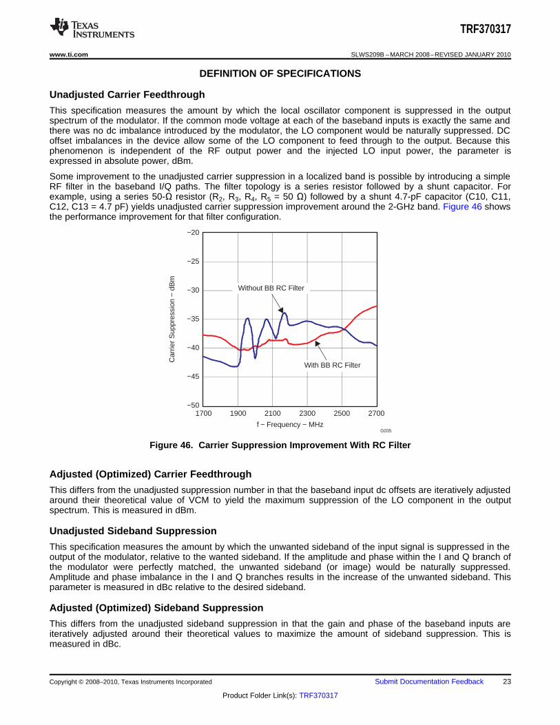
Some improvement to the unadjusted carrier suppression in a localized band is possible by introducing a simpleRF filter in the baseband I/Q paths. The filter topology is a series resistor followed by a shunt capacitor. Forexample, using a series 50-Ω resistor (R2, R3, R4, R5 = 50 Ω) followed by a shunt 4.7-pF capacitor (C10, C11,C12, C13 = 4.7 pF) yields unadjusted carrier suppression improvement around the 2-GHz band. Figure 46 showsthe performance improvement for that filter configuration.
Figure 46. Carrier Suppression Improvement With RC Filter
Adjusted (Optimized) Carrier Feedthrough
This differs from the unadjusted suppression number in that the baseband input dc offsets are iteratively adjustedaround their theoretical value of VCM to yield the maximum suppression of the LO component in the outputspectrum. This is measured in dBm.
Unadjusted Sideband Suppression
This specification measures the amount by which the unwanted sideband of the input signal is suppressed in theoutput of the modulator, relative to the wanted sideband. If the amplitude and phase within the I and Q branch ofthe modulator were perfectly matched, the unwanted sideband (or image) would be naturally suppressed.Amplitude and phase imbalance in the I and Q branches results in the increase of the unwanted sideband. Thisparameter is measured in dBc relative to the desired sideband.
Adjusted (Optimized) Sideband Suppression
This differs from the unadjusted sideband suppression in that the gain and phase of the baseband inputs areiteratively adjusted around their theoretical values to maximize the amount of sideband suppression. This ismeasured in dBc.
Copyright © 2008–2010, Texas Instruments Incorporated Submit Documentation Feedback 23
Product Folder Link(s): TRF370317

f
f
fn
f
f
LO
LSBn
BBn
3rdH/L
2ndH/L
BBn
BBn
BBn
BBn
BBn
BBn
rd
rd
rd
rd
rd
rd
3
2
rd
nd
= Baseband Frequency
= RF Frequency
= 3 Order Intermodulation Product Frequency (High Side/Low Side)
= 2 Order
rd
ndIntermodulation Product (High Side/Low Side)
= Local Oscillator Frequency
= Lower Sideband Frequency
BBn
rd
BBn
BBn
BBn
BBn
BBn
rd
rd
rd
rd
rd
Unw
ante
d Sideb
and
2
Ord
er IM
nd 3Ord
er IM
rd
Des
ired
Signa
l
LSB2 = LO
–fBB2
LSB1 = LO
–fBB1
LO f
= (f
–f
) + LO
2ndL
BB2
BB1
f
= 2f1–
f2
3rdL
f1 = f
+ LO
BB1
f2 = f
+ LO
BB2
f
= 2f2–
f1
3rdH
f
= (f
+ f
) + LO
2ndH
BB2
BB1
M0104-01
TRF370317
SLWS209B –MARCH 2008–REVISED JANUARY 2010 www.ti.com
Suppressions Over Temperature
This specification assumes that the user has gone though the optimization process for the suppression inquestion, and set the optimal settings for the I, Q inputs. This specification then measures the suppression whentemperature conditions change after the initial calibration is done.
Figure 47 shows a simulated output and illustrates the respective definitions of various terms used in this datasheet.
Figure 47. Graphical Illustration of Common Terms
24 Submit Documentation Feedback Copyright © 2008–2010, Texas Instruments Incorporated
Product Folder Link(s): TRF370317

TRF370317
www.ti.com SLWS209B –MARCH 2008–REVISED JANUARY 2010
REVISION HISTORY
NOTE: Page numbers for previous revisions may differ from page numbers in the current version.
Changes from Revision A (June, 2008) to Revision B Page
• Added electrostatic discharge parameters to Absolute Maximum Ratings table ................................................................. 3
• Added ESD Sensitivity section ........................................................................................................................................... 18
Changes from Original (March 2008) to Revision A Page
• Added ACPR graph to Typical Characteristics based on customers' requests .................................................................. 16
• Added ACPR graph to Typical Characteristics based on customers' requests .................................................................. 16
Copyright © 2008–2010, Texas Instruments Incorporated Submit Documentation Feedback 25
Product Folder Link(s): TRF370317

PACKAGE OPTION ADDENDUM
www.ti.com 10-Dec-2020
Addendum-Page 1
PACKAGING INFORMATION
Orderable Device Status(1)
Package Type PackageDrawing
Pins PackageQty
Eco Plan(2)
Lead finish/Ball material
(6)
MSL Peak Temp(3)
Op Temp (°C) Device Marking(4/5)
Samples
TRF370317IRGER ACTIVE VQFN RGE 24 3000 RoHS & Green NIPDAU Level-2-260C-1 YEAR -40 to 85 TRF370317
TRF370317IRGET ACTIVE VQFN RGE 24 250 RoHS & Green NIPDAU Level-2-260C-1 YEAR -40 to 85 TRF370317
(1) The marketing status values are defined as follows:ACTIVE: Product device recommended for new designs.LIFEBUY: TI has announced that the device will be discontinued, and a lifetime-buy period is in effect.NRND: Not recommended for new designs. Device is in production to support existing customers, but TI does not recommend using this part in a new design.PREVIEW: Device has been announced but is not in production. Samples may or may not be available.OBSOLETE: TI has discontinued the production of the device.
(2) RoHS: TI defines "RoHS" to mean semiconductor products that are compliant with the current EU RoHS requirements for all 10 RoHS substances, including the requirement that RoHS substancedo not exceed 0.1% by weight in homogeneous materials. Where designed to be soldered at high temperatures, "RoHS" products are suitable for use in specified lead-free processes. TI mayreference these types of products as "Pb-Free".RoHS Exempt: TI defines "RoHS Exempt" to mean products that contain lead but are compliant with EU RoHS pursuant to a specific EU RoHS exemption.Green: TI defines "Green" to mean the content of Chlorine (Cl) and Bromine (Br) based flame retardants meet JS709B low halogen requirements of <=1000ppm threshold. Antimony trioxide basedflame retardants must also meet the <=1000ppm threshold requirement.
(3) MSL, Peak Temp. - The Moisture Sensitivity Level rating according to the JEDEC industry standard classifications, and peak solder temperature.
(4) There may be additional marking, which relates to the logo, the lot trace code information, or the environmental category on the device.
(5) Multiple Device Markings will be inside parentheses. Only one Device Marking contained in parentheses and separated by a "~" will appear on a device. If a line is indented then it is a continuationof the previous line and the two combined represent the entire Device Marking for that device.
(6) Lead finish/Ball material - Orderable Devices may have multiple material finish options. Finish options are separated by a vertical ruled line. Lead finish/Ball material values may wrap to twolines if the finish value exceeds the maximum column width.
Important Information and Disclaimer:The information provided on this page represents TI's knowledge and belief as of the date that it is provided. TI bases its knowledge and belief on informationprovided by third parties, and makes no representation or warranty as to the accuracy of such information. Efforts are underway to better integrate information from third parties. TI has taken andcontinues to take reasonable steps to provide representative and accurate information but may not have conducted destructive testing or chemical analysis on incoming materials and chemicals.TI and TI suppliers consider certain information to be proprietary, and thus CAS numbers and other limited information may not be available for release.
In no event shall TI's liability arising out of such information exceed the total purchase price of the TI part(s) at issue in this document sold by TI to Customer on an annual basis.

PACKAGE OPTION ADDENDUM
www.ti.com 10-Dec-2020
Addendum-Page 2

TAPE AND REEL INFORMATION
*All dimensions are nominal
Device PackageType
PackageDrawing
Pins SPQ ReelDiameter
(mm)
ReelWidth
W1 (mm)
A0(mm)
B0(mm)
K0(mm)
P1(mm)
W(mm)
Pin1Quadrant
TRF370317IRGER VQFN RGE 24 3000 330.0 12.4 4.3 4.3 1.5 8.0 12.0 Q1
TRF370317IRGET VQFN RGE 24 250 330.0 12.4 4.3 4.3 1.5 8.0 12.0 Q1
PACKAGE MATERIALS INFORMATION
www.ti.com 22-Nov-2018
Pack Materials-Page 1
*All dimensions are nominal
Device Package Type Package Drawing Pins SPQ Length (mm) Width (mm) Height (mm)
TRF370317IRGER VQFN RGE 24 3000 367.0 367.0 38.0
TRF370317IRGET VQFN RGE 24 250 367.0 367.0 38.0
PACKAGE MATERIALS INFORMATION
www.ti.com 22-Nov-2018
Pack Materials-Page 2

GENERIC PACKAGE VIEW
Images above are just a representation of the package family, actual package may vary.Refer to the product data sheet for package details.
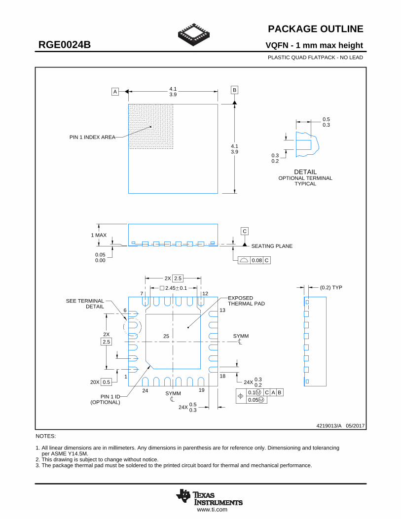
RGE 24 VQFN - 1 mm max heightPLASTIC QUAD FLATPACK - NO LEAD
4204104/H
www.ti.com
PACKAGE OUTLINE
C
SEE TERMINALDETAIL
24X 0.30.2
2.45 0.1
24X 0.50.3
1 MAX
(0.2) TYP
0.050.00
20X 0.5
2X2.5
2X 2.5
A 4.13.9
B
4.13.9
0.30.2
0.50.3
VQFN - 1 mm max heightRGE0024BPLASTIC QUAD FLATPACK - NO LEAD
4219013/A 05/2017
PIN 1 INDEX AREA
0.08 C
SEATING PLANE
1
6 13
18
7 12
24 19
(OPTIONAL)PIN 1 ID
0.1 C A B0.05
EXPOSEDTHERMAL PAD
25 SYMM
SYMM
NOTES: 1. All linear dimensions are in millimeters. Any dimensions in parenthesis are for reference only. Dimensioning and tolerancing per ASME Y14.5M. 2. This drawing is subject to change without notice. 3. The package thermal pad must be soldered to the printed circuit board for thermal and mechanical performance.
SCALE 3.000
DETAILOPTIONAL TERMINAL
TYPICAL

www.ti.com
EXAMPLE BOARD LAYOUT
0.07 MINALL AROUND
0.07 MAXALL AROUND
24X (0.25)
24X (0.6)
( 0.2) TYPVIA
20X (0.5)
(3.8)
(3.8)
( 2.45)
(R0.05)TYP
(0.975) TYP
VQFN - 1 mm max heightRGE0024BPLASTIC QUAD FLATPACK - NO LEAD
4219013/A 05/2017
SYMM
1
6
7 12
13
18
1924
SYMM
LAND PATTERN EXAMPLEEXPOSED METAL SHOWN
SCALE:15X
NOTES: (continued) 4. This package is designed to be soldered to a thermal pad on the board. For more information, see Texas Instruments literature number SLUA271 (www.ti.com/lit/slua271).5. Vias are optional depending on application, refer to device data sheet. If any vias are implemented, refer to their locations shown on this view. It is recommended that vias under paste be filled, plugged or tented.
25
SOLDER MASKOPENING
METAL UNDERSOLDER MASK
SOLDER MASKDEFINED
EXPOSEDMETAL
METAL
SOLDER MASKOPENING
SOLDER MASK DETAILS
NON SOLDER MASKDEFINED
(PREFERRED)
EXPOSEDMETAL

www.ti.com
EXAMPLE STENCIL DESIGN
24X (0.6)
24X (0.25)
20X (0.5)
(3.8)
(3.8)
4X ( 1.08)
(0.64)TYP
(0.64) TYP
(R0.05) TYP
VQFN - 1 mm max heightRGE0024BPLASTIC QUAD FLATPACK - NO LEAD
4219013/A 05/2017
NOTES: (continued) 6. Laser cutting apertures with trapezoidal walls and rounded corners may offer better paste release. IPC-7525 may have alternate design recommendations.
25
SYMM
METALTYP
SOLDER PASTE EXAMPLEBASED ON 0.125 mm THICK STENCIL
EXPOSED PAD 25
78% PRINTED SOLDER COVERAGE BY AREA UNDER PACKAGESCALE:20X
SYMM
1
6
7 12
13
18
1924

IMPORTANT NOTICE AND DISCLAIMER
TI PROVIDES TECHNICAL AND RELIABILITY DATA (INCLUDING DATASHEETS), DESIGN RESOURCES (INCLUDING REFERENCE DESIGNS), APPLICATION OR OTHER DESIGN ADVICE, WEB TOOLS, SAFETY INFORMATION, AND OTHER RESOURCES “AS IS” AND WITH ALL FAULTS, AND DISCLAIMS ALL WARRANTIES, EXPRESS AND IMPLIED, INCLUDING WITHOUT LIMITATION ANY IMPLIED WARRANTIES OF MERCHANTABILITY, FITNESS FOR A PARTICULAR PURPOSE OR NON-INFRINGEMENT OF THIRD PARTY INTELLECTUAL PROPERTY RIGHTS.These resources are intended for skilled developers designing with TI products. You are solely responsible for (1) selecting the appropriate TI products for your application, (2) designing, validating and testing your application, and (3) ensuring your application meets applicable standards, and any other safety, security, or other requirements. These resources are subject to change without notice. TI grants you permission to use these resources only for development of an application that uses the TI products described in the resource. Other reproduction and display of these resources is prohibited. No license is granted to any other TI intellectual property right or to any third party intellectual property right. TI disclaims responsibility for, and you will fully indemnify TI and its representatives against, any claims, damages, costs, losses, and liabilities arising out of your use of these resources.TI’s products are provided subject to TI’s Terms of Sale (www.ti.com/legal/termsofsale.html) or other applicable terms available either on ti.com or provided in conjunction with such TI products. TI’s provision of these resources does not expand or otherwise alter TI’s applicable warranties or warranty disclaimers for TI products.
Mailing Address: Texas Instruments, Post Office Box 655303, Dallas, Texas 75265Copyright © 2020, Texas Instruments Incorporated