– 1 – data converters sample-and-holdprofessor y. chiu eect 7327fall 2014 sample-and-hold (s/h)...
TRANSCRIPT

– 1 –
Data Converters Sample-and-HoldProfessor Y. Chiu
EECT 7327Fall 2014
Sample-and-Hold (S/H) Basics

ZOH vs. Track-and-Hold (T/H)
– 2 –
Data Converters Sample-and-HoldProfessor Y. Chiu
EECT 7327Fall 2014
• Zero acquisition time• Infinite bandwidth• Not realistic
• T/2 acquisition time• Finite bandwidth• Practical
V(t)
t0 T 2TT
V(t)
t0T/2
T 2T
H T H T H T H T H T

A Simple T/H (Top-Plate Sampling)
– 3 –
Data Converters Sample-and-HoldProfessor Y. Chiu
EECT 7327Fall 2014
Vo
Ф
CS
RS
Vi
• MOS technology is naturally suitable for implementing T/H• The lowpass SC network determines the tracking bandwidth• Non-idealities: signal-dependent Ron, charge injection, aperture, etc.
Ron
0 VDDVi
VTnVTp
PMOS
NMOS
CMOS
ithDDox1
on VVVL
WμCR

Tracking Bandwidth (TBW)
– 4 –
Data Converters Sample-and-HoldProfessor Y. Chiu
EECT 7327Fall 2014
Ron
CSVi Vo
RS Ron
0 VDDVi SonS CRR1TBW
• Tracking bandwidth determines how promptly Vo can follow Vi
• Typically TBW is many times greater than the max signal bandwidth• What’s wrong with the concept of “linear filtering” if Ron is constant?
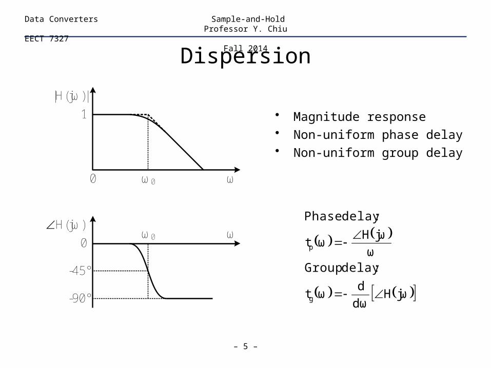
Dispersion
– 5 –
Data Converters Sample-and-HoldProfessor Y. Chiu
EECT 7327Fall 2014
jωHdω
dωt
:delay Groupω
jωHωt
:delay Phase
g
p
• Magnitude response• Non-uniform phase delay• Non-uniform group delay
|H(jω)|
1
ω0
H(jω)
-45°
0
-90°
ω0
ωω0

Dispersion
– 6 –
Data Converters Sample-and-HoldProfessor Y. Chiu
EECT 7327Fall 2014
• Waveform is not very sensitive to the lowpass magnitude response as long as the signal bandwidth is on the order of TBW
• Waveform distortion is mainly due to non-uniform phase and group delays
Ron
CSVi Vo
RS
t t
Signal-Dependent Ron
– 7 –
Data Converters Sample-and-HoldProfessor Y. Chiu
EECT 7327Fall 2014
Vo
Ф
CS
RS
Vi
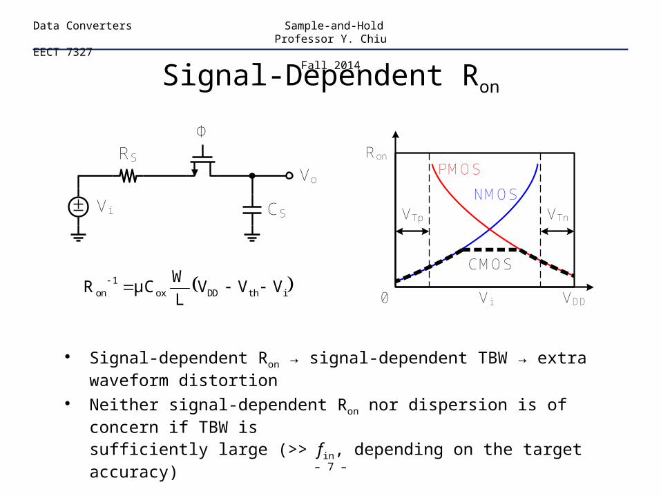
• Signal-dependent Ron → signal-dependent TBW → extra waveform distortion
• Neither signal-dependent Ron nor dispersion is of concern if TBW is
sufficiently large (>> fin, depending on the target accuracy)
Ron
0 VDDVi
VTnVTp
PMOS
NMOS
CMOS
ithDDox1
on VVVL
WμCR

Ideal T/H
– 8 –
Data Converters Sample-and-HoldProfessor Y. Chiu
EECT 7327Fall 2014
• Sufficient tracking bandwidth → negligible tracking error• Well-defined sampling instant (asserted by clock rising/falling edge)• Zero track-mode and hold-mode offset errors
V(t)
tTrack HoldHold

T/H Errors (Track Mode)
– 9 –
Data Converters Sample-and-HoldProfessor Y. Chiu
EECT 7327Fall 2014
• Finite tracking bandwidth → tracking error, T/H memory• Track-mode offset, gain error, and nonlinearity
V(t)
t
δ1δ2
Droop
Track HoldHold
Δt
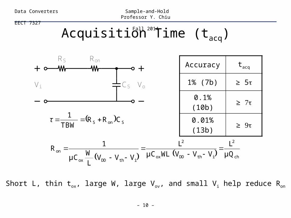
Acquisition Time (tacq)
– 10 –
Data Converters Sample-and-HoldProfessor Y. Chiu
EECT 7327Fall 2014
Ron
CSVi Vo
RS
SonS CRRTBW
1τ
Short L, thin tox, large W, large Vov, and small Vi help reduce Ron
Accuracy tacq
1% (7b) ≥ 5t
0.1% (10b) ≥ 7t
0.01% (13b) ≥ 9t
ch
2
ithDDox
2
ithDDox
on μQ
L
VVVWLμC
L
VVVLW
μC
1R

T/H Errors (T-to-H Transition)
– 11 –
Data Converters Sample-and-HoldProfessor Y. Chiu
EECT 7327Fall 2014
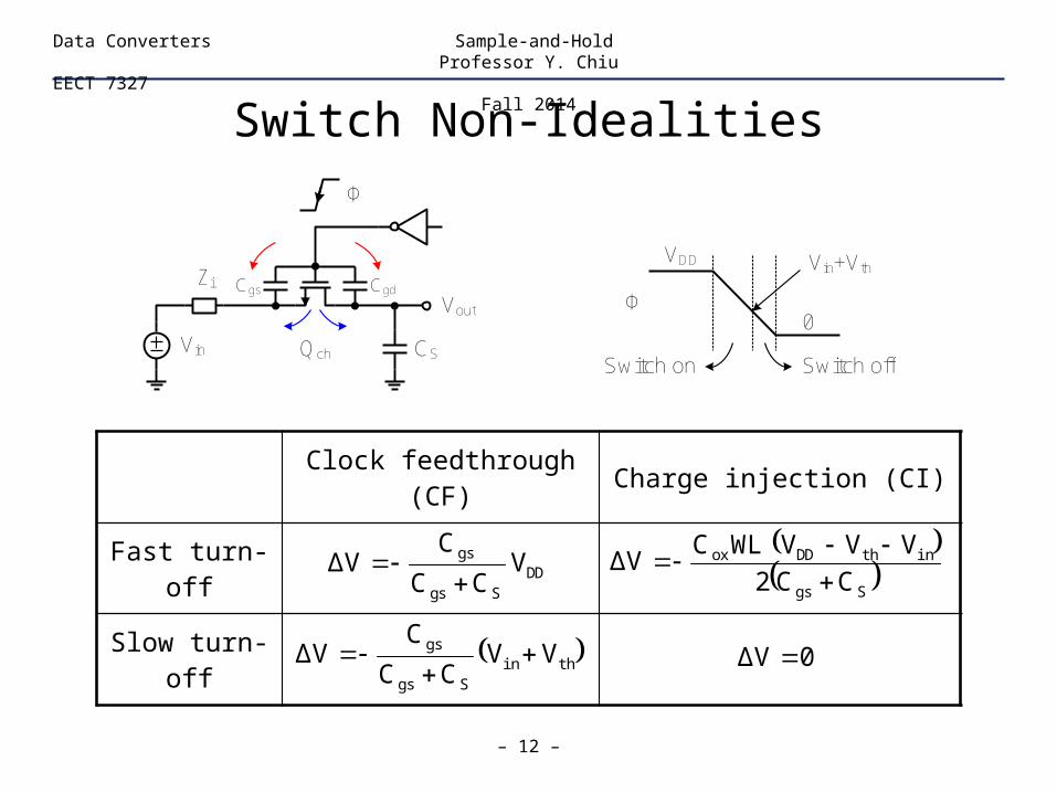
• Pedestal error (often signal-dependent) resulted from switch turn-offnonidealities (clock feedthrough and charge injection)
• Aperture delay – the delay Δt b/t hold command and hold action• Aperture jitter – the random variation in Δt (i.e., sampling clock jitter)
V(t)
t
δ1δ2
Droop
Track HoldHold
Δt
Switch Non-Idealities
– 12 –
Data Converters Sample-and-HoldProfessor Y. Chiu
EECT 7327Fall 2014
Ф
VDD
0
Vin+Vth
Switch on Switch off
Vout
Ф
CS
Zi
Vin
CgdCgs
Qch
Clock feedthrough (CF) Charge injection (CI)
Fast turn-off
Slow turn-off
DDSgs
gs VCC
CΔV
Sgs
inthDDox
CC2
VVVWLCΔV
thinSgs
gs VVCC
CΔV
0ΔV
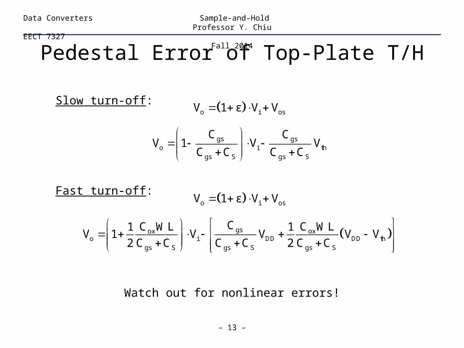
Pedestal Error of Top-Plate T/H
– 13 –
Data Converters Sample-and-HoldProfessor Y. Chiu
EECT 7327Fall 2014
o i os
gsox oxo i DD DD th
gs S gs S gs S
V 1 ε V V
CC WL C WL1 1V 1 V V V V
2 C C C C 2 C C
o i os
gs gso i th
gs S gs S
V 1 ε V V
C CV 1 V V
C C C C
Slow turn-off:
Fast turn-off:
Watch out for nonlinear errors!
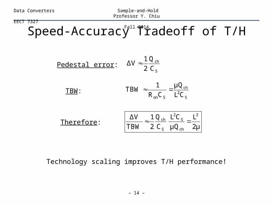
Speed-Accuracy Tradeoff of T/H
– 14 –
Data Converters Sample-and-HoldProfessor Y. Chiu
EECT 7327Fall 2014
S
ch
C
Q
2
1ΔV Pedestal error:
TBW:S
2ch
Son CL
μQ
CR
1TBW
2μ
L
μQ
CL
C
Q
2
1
TBW
ΔV 2
ch
S2
S
ch Therefore:
Technology scaling improves T/H performance!

Aperture Delay (Δt)
– 15 –
Data Converters Sample-and-HoldProfessor Y. Chiu
EECT 7327Fall 2014
• Fixed aperture delay is usually not of problem in a single-path T/H• Non-uniform aperture delays among time-interleaved T/H paths cause
significant errors (Δt1, Δt2… are also called sampling clock skew)
CH 1
CH 2
Φ1
Φ2
Vin
Φ1
Φ2

Aperture Jitter
– 16 –
Data Converters Sample-and-HoldProfessor Y. Chiu
EECT 7327Fall 2014
V(t)
t
δV
Track Hold
δt
dVdt
Ref: M. Shinagawa, Y. Akazawa, and T. Wakimoto, “Jitter analysis of high-speed sampling systems,” IEEE Journal of Solid-State Circuits, vol. 25, issue 1, pp. 220-224, 1990.

Aperture Jitter
– 17 –
Data Converters Sample-and-HoldProfessor Y. Chiu
EECT 7327Fall 2014
2
σωAδt
2
ωAdtωtcosAω
T
1δttε
onary"Cyclostati"ωtAcosωδtωtAsintVtε2
t22
222T
0
222
i
i
2
V t Asin ω t δt
Asin ωt cos ωδt Acos ωt sin ωδt
ωδt ωδt ωδtAsin ωt 1 sin Acos ωt 2sin cos
2 2 2
Asin ωt ωδt Acos ωt for small δt
2t
2
2t
222
σω
1
2σωA
2A
SNR

Aperture Jitter
– 18 –
Data Converters Sample-and-HoldProfessor Y. Chiu
EECT 7327Fall 2014
106
107
108
109
0
20
40
60
80
100
120
140
Input Freq [Hz]
SN
R [
dB
]
t = 0.1ps
t = 1ps
t = 10ps
t = 100ps
t10 ωσLOG20SNR

T/H Errors (Hold Mode)
– 19 –
Data Converters Sample-and-HoldProfessor Y. Chiu
EECT 7327Fall 2014
• Hold-mode droop caused by off-switch/diode/gate leakage• Hold-mode input feedthrough (i.e., due to capacitive coupling)
V(t)
t
δ1δ2
Droop
Track HoldHold
Δt

Evaluating T/H Performance
– 20 –
Data Converters Sample-and-HoldProfessor Y. Chiu
EECT 7327Fall 2014
kT/C noise:
SNDR: 2ε
222
2N
2i
Vδt2ωA
V
VSNDR
S0
2
S
2N C
kTdf
RCfj2π1
14kTRV
Noise Distortion
CS √kT/C
100pF 6.4μV
1pF 64μV
10fF 640μV
T = 300K
Jitter
– 21 –
Data Converters Sample-and-HoldProfessor Y. Chiu
EECT 7327Fall 2014
MOS S/H Techniques

Simple Top-Plate Sampling
– 22 –
Data Converters Sample-and-HoldProfessor Y. Chiu
EECT 7327Fall 2014
Vo
Ф
CS
RS
Vi
Pros• Simple, minimum number of devices• Potentially wideband, zero track-mode offset
Cons• Signal-dependent tracking bandwidth• Signal-dependent charge injection and clock feedthrough• Signal-dependent aperture delay (sampling point)

Signal-Dependent Aperture Delay
– 23 –
Data Converters Sample-and-HoldProfessor Y. Chiu
EECT 7327Fall 2014
• Non-uniform sampling due to signal-dependent aperture delay causes distortion in top-plate S/H
• Sharp clock edge and small Vin mitigate the delay variation
Ф
VDD
0
Vi+Vth(Vi)
Switch on Switch off
Vth(Vi)
i
io
V t Asin ωt
V tV t Asin ω t
SR

Signal Distortion
– 24 –
Data Converters Sample-and-HoldProfessor Y. Chiu
EECT 7327Fall 2014
ωt2sinA2
1
SR
ωωtAcos
SR
ωtAsinωtε
ωtAcosSR
VωtVtVtε
2
ioi
io
i i
i i
VV t Asin ω t
SR
V VAsin ωt cos ω Acos ωt sin ω
SR SR
V VAsin ωt ω Acos ωt for small
SR SR
22
2
22
2
ωA
SR4
2
SR2ωA
2A
SDR
← 2nd-order
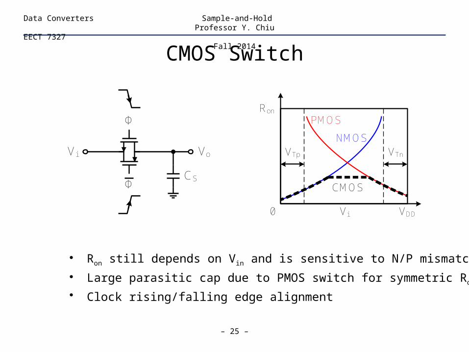
CMOS Switch
– 25 –
Data Converters Sample-and-HoldProfessor Y. Chiu
EECT 7327Fall 2014
• Ron still depends on Vin and is sensitive to N/P mismatch
• Large parasitic cap due to PMOS switch for symmetric Ron
• Clock rising/falling edge alignment
Ron
0 VDDVi
VTnVTp
PMOS
NMOS
CMOS
Vo
CS
Vi
Ф
Ф

Clock Bootstrapping
– 26 –
Data Converters Sample-and-HoldProfessor Y. Chiu
EECT 7327Fall 2014
• Constant gate overdrive voltage VGS = VDD for the switch
• Ron is not dependent on Vin to the first order (body effect?)
• NMOS device only with less parasitic capacitance
Ron
0 VDDVi
OutInM1
VDD
Φ Φ

Clock Bootstrapping
– 27 –
Data Converters Sample-and-HoldProfessor Y. Chiu
EECT 7327Fall 2014
Out
M6
CC2C1
M5
Φ
ΦΦ
Φ
Φ
Φ
In
M4 M3
M2
M1
VDD
VSS
Φ
Ref: A. M. Abo and P. R. Gray, “A 1.5-V, 10-bit, 14.3-MS/s CMOS pipeline ADC,” IEEE Journal of Solid-State Circuits, vol. 34, issue 5, pp. 599-606, 1999.

Clock Bootstrapping (Φ=0)
– 28 –
Data Converters Sample-and-HoldProfessor Y. Chiu
EECT 7327Fall 2014
Out
C Φ
Φ
Φ
In
M2
M1
Φ
VDD
VSS
Out
C
Φ
Φ
In
M3
M1
M2Φ
Φ

Clock Bootstrapping (Φ=1)
– 29 –
Data Converters Sample-and-HoldProfessor Y. Chiu
EECT 7327Fall 2014
Out
C
Φ
Φ
In
M3
M1
M2Φ
Φ
Out
C Φ
Φ
Φ
In
M2
M1
Φ
VDD
VSS
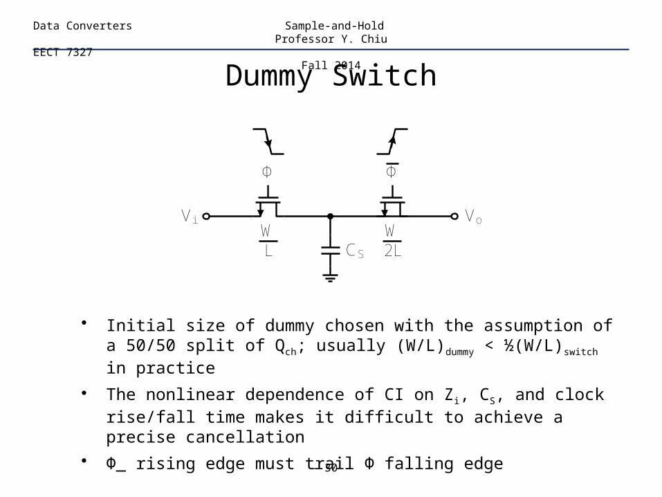
Dummy Switch
– 30 –
Data Converters Sample-and-HoldProfessor Y. Chiu
EECT 7327Fall 2014
• Initial size of dummy chosen with the assumption of a 50/50 split of Qch; usually (W/L)dummy < ½(W/L)switch in practice
• The nonlinear dependence of CI on Zi, CS, and clock rise/fall time makes it difficult to achieve a precise cancellation
• Ф_ rising edge must trail Ф falling edge
Vo
Ф
WL CS
W2L
Ф
Vi
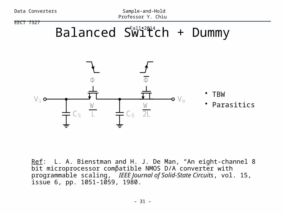
Balanced Switch + Dummy
– 31 –
Data Converters Sample-and-HoldProfessor Y. Chiu
EECT 7327Fall 2014
Vo
Ф
WL CS
W2L
Ф
Vi
CS
Ref: L. A. Bienstman and H. J. De Man, “An eight-channel 8 bit microprocessor compatible NMOS D/A converter with programmable scaling,” IEEE Journal of Solid-State Circuits, vol. 15, issue 6, pp. 1051-1059, 1980.
• TBW• Parasitics

Fully-Differential T/H
– 32 –
Data Converters Sample-and-HoldProfessor Y. Chiu
EECT 7327Fall 2014
• All even-order distortions cancelled, including the signal-dependent aperture delay-induced distortion
• Actual cancellation limited by P/N mismatch (1-10% typically)
fin 0.5GHz
VDD 1.8V
tf 0.1ns
A (Vin) 0.5V
SDR (SE) 20-30 dB
SDR (DF) 40-50 dB
Vo+
CS+
Vi+
Vo-
CS-
Vi-
Ф
M1
M2
E.g.
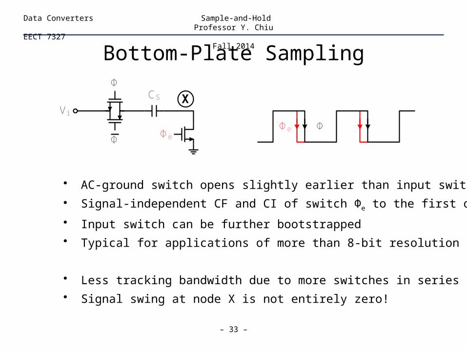
Bottom-Plate Sampling
– 33 –
Data Converters Sample-and-HoldProfessor Y. Chiu
EECT 7327Fall 2014
• AC-ground switch opens slightly earlier than input switches
• Signal-independent CF and CI of switch Φe to the first order!
• Input switch can be further bootstrapped
• Typical for applications of more than 8-bit resolution
• Less tracking bandwidth due to more switches in series
• Signal swing at node X is not entirely zero!
Фe Ф
CS
Vi
Ф
ФФe
X

– 34 –
Data Converters Sample-and-HoldProfessor Y. Chiu
EECT 7327Fall 2014
Sample-and-Hold Amplifier(SHA)

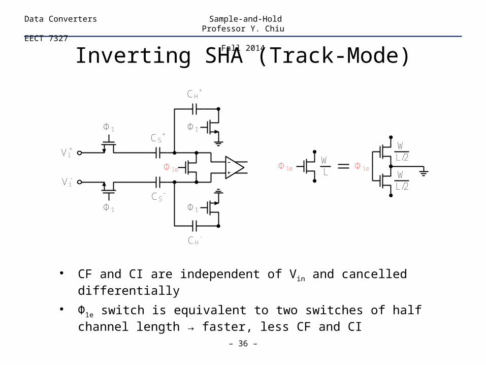
Inverting SHA
– 35 –
Data Converters Sample-and-HoldProfessor Y. Chiu
EECT 7327Fall 2014
Vi+ Vo
+
Vo-Vi
-
CS+
Ф2CS
-
Ф2
Ф1e
Ф1
Ф1
Ф2
CH+
CH-
Ф1
Ф1
• Inverting, closed-loop gain determined by the ratio CS/CH
• CMOS or bootstrapped switches are required when passing signals with large swing (where?)
Ф1eФ1
Ф2
T H
Inverting SHA (Track-Mode)
– 36 –
Data Converters Sample-and-HoldProfessor Y. Chiu
EECT 7327Fall 2014
• CF and CI are independent of Vin and cancelled differentially
• Φ1e switch is equivalent to two switches of half channel length → faster, less CF and CI
Vi+
Vi-
CS+
CS-
Ф1e
Ф1
Ф1
CH+
CH-
Ф1
Ф1
WL
Ф1e Ф1e
WL/2
WL/2

Inverting SHA (Hold-Mode)
– 37 –
Data Converters Sample-and-HoldProfessor Y. Chiu
EECT 7327Fall 2014
• For 1X gain (CS = CH), the feedback factor is about 1/2
• Floating switch Φ2 in hold-mode → flexible input common mode
• Useful for single-ended to differential conversion
Vo+
Vo-
CS+
Ф2CS
-
Ф2
Ф2
CH+
CH-
• CM?• DM?

Differential Mode
– 38 –
Data Converters Sample-and-HoldProfessor Y. Chiu
EECT 7327Fall 2014
• DM charge transfer is complete
Vo+
Vo-
CS+
Ф2CS
-
Ф2
Ф2
CH+
CH-
DM half circuit
Vo+
CS
Ф2
Adm
CH
Vi,dmФ2

Common Mode
– 39 –
Data Converters Sample-and-HoldProfessor Y. Chiu
EECT 7327Fall 2014
• CM charge is not transferred!
Vo+
Vo-
CS+
Ф2CS
-
Ф2
Ф2
CH+
CH-
CM half circuit
Vo
+
CS
Ф2
Acm
CH
Vi,cm

Flip-Around SHA
– 40 –
Data Converters Sample-and-HoldProfessor Y. Chiu
EECT 7327Fall 2014
• Non-inverting, 1X closed-loop gain
• Close-to-unity feedback factor in hold mode
• CF/CI independent of Vin and cancelled differentially
Vi+ Vo
+
Vo-Vi
-
CS+
Ф2Ф1eCS
-
Ф2Ф1e
Ф1
Ф1
Ф1eФ1
Ф2
T H