© 2001 ® tuesday, 19 june 2001 1 nios tm advanced training session ii memory accesses
Post on 22-Dec-2015
215 views
TRANSCRIPT

1 © 2001 ®
Tuesday, 19 June 2001Tuesday, 19 June 2001
NiosTM Advanced Training
SESSION IISESSION II
Memory Accesses

2 © 2001 ®
Memory Access Instructions
LD, ST LDP, STP LDS, STS PFX
EXT16D EXT16S EXT8D EXT8S FILL16 FILL8

3 © 2001 ®
Prefixable Instructions PFX
The following instructions can be extented by PFX instruction:– ADDI, AND, ANDN, CMPi, MOVHi, MOVi, OR, SUBi, XOR
LD, LDP, LDS, ST, STP or STS DO NOT follow the same mechanism
0
15
0
14
1
13
1
12
0
11
1
10
X
9
X
8
X
7
X
6
X
5
X
4
X
3
X
2
X
1
X
0
IMM5IMM5 Ra
Example: MOVI, MOVHI instruction
1
15
0
14
0
13
1
12
1
11
X
10
X
9
X
8
X
7
X
6
X
5
X
4
X
3
X
2
X
1
X
0
IMM11IMM11
PFX intruction
PFX IMM11
MOVHI IMM5 Ra = Ra = PFX IMM11
MOVI IMM5
IMM11[15..5]IMM11[15..5] IMM5IMM5
31 16 2021
IMM11[15..5]IMM11[15..5] IMM5IMM5
45 0 15

4 © 2001 ®
The best way to use PFX instruction
PFX %hi(100) ; Extract bits 5..15 of x
MOVI %g1, %lo(100) ; Extract low 5 bits of x
PFX %xhi(100) ; Extract bits 21..31 of x
MOVHI %g1, %xlo(100) ; Extract bits 16..20 of x

5 © 2001 ®
Addressing Modes – Simple
LDLD = Load data from memory Ra = Mem[Rb] STST = Store data to memory Mem[Rb] = Ra
If prefixed by PFX:
Ra = MEM[ Rb + 4.s(K)]
X
15
X
14
X
13
X
12
X
11
X
10
X
9
X
8
X
7
X
6
X
5
X
4
X
3
X
2
X
1
X
0
Index of Rb Index of Ra
Instruction Fields
6 © 2001 ®
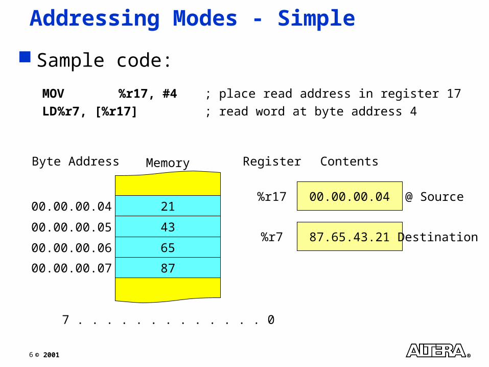
Addressing Modes - Simple
Sample code:
MOV %r17, #4 ; place read address in register 17
LD %r7, [%r17] ; read word at byte address 4
21
MemoryByte Address
00.00.00.04
00.00.00.05 43
65
87
00.00.00.06
00.00.00.07
7 . . . . . . . . . . . . . 0
Register Contents
87.65.43.21%r7 Destination
00.00.00.04%r17 @ Source

7 © 2001 ®
Addressing Modes - Simple (with Offset)
00
MemoryByte Address
00.00.00.24
00.00.00.25 EF
CD
AB
00.00.00.26
00.00.00.27
7 . . . . . . . . . . . . . 0
Register Contents
DestinationAB.CD.EF.00%r7
00.00.00.08%i3
00.00.00.07%K Offset
Sample code:
MOV %i3, #8 ; place read address (8) in register %i3
PFX #7 ; offset is 7 words (28 bytes, 0x1C)
LD %r7, [%i3] ; read word at byte address 0x24
00.00.00.24 @ Source

8 © 2001 ®
Addressing Modes - Pointer
LDPLDP = Load with pointer addressing Ra = Mem[ Rp + 4.IMM5 ] STPSTP = Store with pointer addressing Mem[ Rp + 4.IMM5 ] = Ra
Rp must be (r16, r17, r18 or r19r16, r17, r18 or r19)
If prefixed by PFX:
Ra = MEM[ Rp + 4.s(K:IMM5)]
Instruction Fields
X
15
X
14
X
13
X
12 11 10
X
9
X
8
X
7
X
6
X
5
X
4
X
3
X
2
X
1
X
0
IMM5 Index of RaRpRp

9 © 2001 ®
Addressing Modes - Pointer
32
MemoryByte Address
00.00.00.2C
00.00.00.2D 54
76
98
00.00.00.2E
00.00.00.2F
7 . . . . . . . . . . . . . 0
Register Contents
00.00.00.2C @ Destination
00.00.00.20%r16 Base Pointer
00.00.00.0C#3*4 IMM Offset
98.76.54.32%r3 Source
Sample code:
MOV %r16, #0x20 ; set base pointer to 0x20
STP [%r16, #3], %r3 ; store word to byte address 0x2C

10
© 2001 ®
Addressing Modes - Pointer (with Offset)
Sample code:
MOV %r16, #0x20 ; set base pointer to 0x20
PFX %hi(100) ; hi loads upper 11-bits
STP [%r16, %lo(100)], %r3 ; lo loads lower 5-bits
100d = 100d = 15 14 13 12 11 10 9 8 7 6 5 4 3 2 1 0
bb0 0 0 0 0 0 0 0 1 10
K-Register = 3
0 0 1 0 0
IMM5 = 4
11
© 2001 ®
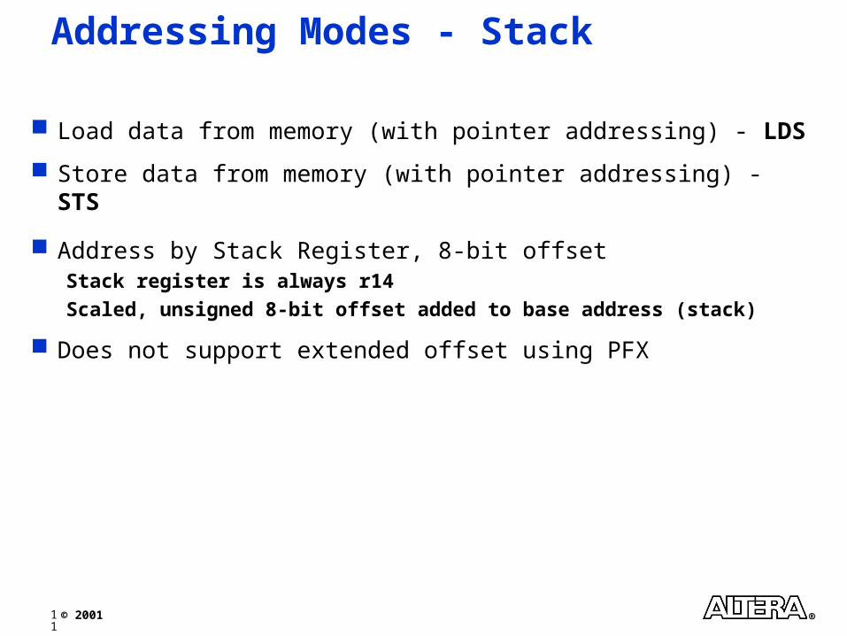
Addressing Modes - Stack
Load data from memory (with pointer addressing) - LDS
Store data from memory (with pointer addressing) - STS
Address by Stack Register, 8-bit offsetStack register is always r14
Scaled, unsigned 8-bit offset added to base address (stack)
Does not support extended offset using PFX

12
© 2001 ®
Instruction Set EXT16D
Assembler Syntax: EXT16D EXT16D %rA, %rB%rA, %rB
Example: LDLD %i3, [%i4]%i3, [%i4]EXT16DEXT16D %i3, %i4%i3, %i4
Half Word 1 Half Word 0
------------------- 0 ------------------- Half Word n
rA before
rA after
rB[1..0]

13
© 2001 ®
Instruction Set EXT8D
Assembler Syntax: EXT8D EXT8D %rA, %rB%rA, %rB
Example: LDLD %i3, [%i4]%i3, [%i4]EXT8DEXT8D %i3, %i4%i3, %i4
Byte 3 Byte 2 Byte 1 Byte 0
rB[1..0]
Byte n------------------------ 0 ------------------------
rA before
rA after

14
© 2001 ®
Instruction Set EXT16S
Assembler Syntax: EXT16S EXT16S %rA, IMM1%rA, IMM1
Example: LDLD %i3, [%i4]%i3, [%i4]EXT16DEXT16D %i3, 1%i3, 1
Half Word 1 Half Word 0
------------------- 0 ------------------- Half Word n
rA before
rA after
IMM1
15
© 2001 ®
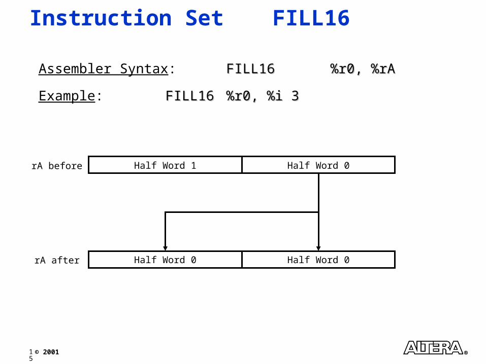
Instruction Set FILL16
Assembler Syntax: FILL16 FILL16 %r0, %rA%r0, %rA
Example: FILL16FILL16 %r0, %i 3%r0, %i 3
Half Word 1 Half Word 0
Half Word 0 Half Word 0
rA before
rA after

16
© 2001 ®
Memory Interface Berkeley Architecture
The Data & Address Busses have to be shared between Data and Instructions
InstructionFetching
InstructionDecoding
ExecutingWriting
Back
General-Purpose Processor Register File
Program Counter
MemoryPRG
Processor
Instructions
MemoryData
Variable,
Stack,
User Data

17
© 2001 ®
Memory Interface Decoder Impact
Design requirementsGuarantee reliable access to external memory
Achieve 50MHz w/o cache
Uses Fast IO on APEX pad~16ns addr-out-to-data-in
Requires 2 clocks when switching between external memory and other devices
18
© 2001 ®
Write cmd
Data
Construction
Address
Construction
Write cmd
Data
Construction
Address
Construction
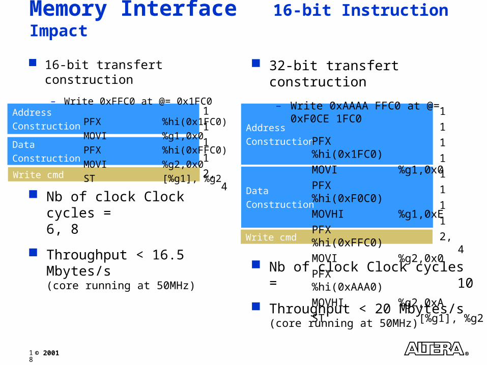
Memory Interface 16-bit Instruction Impact
16-bit transfert construction
– Write 0xFFC0 at @= 0x1FC0
PFX %hi(0x1FC0)
MOVI %g1,0x0
PFX %hi(0xFFC0)
MOVI %g2,0x0
ST [%g1], %g2
32-bit transfert construction
– Write 0xAAAA FFC0 at @= 0xF0CE 1FC0
PFX %hi(0x1FC0)
MOVI %g1,0x0
PFX %hi(0xF0C0)
MOVHI %g1,0xE
PFX %hi(0xFFC0)
MOVI %g2,0x0
PFX %hi(0xAAA0)
MOVHI %g2,0xA
ST [%g1], %g2
Nb of clock Clock cycles = 6, 8
Throughput < 16.5 Mbytes/s(core running at 50MHz)
1
1
1
1
2, 4
1
1
1
1
1
1
1
1
2, 4
Nb of clock Clock cycles = 10
Throughput < 20 Mbytes/s(core running at 50MHz)
19
© 2001 ®
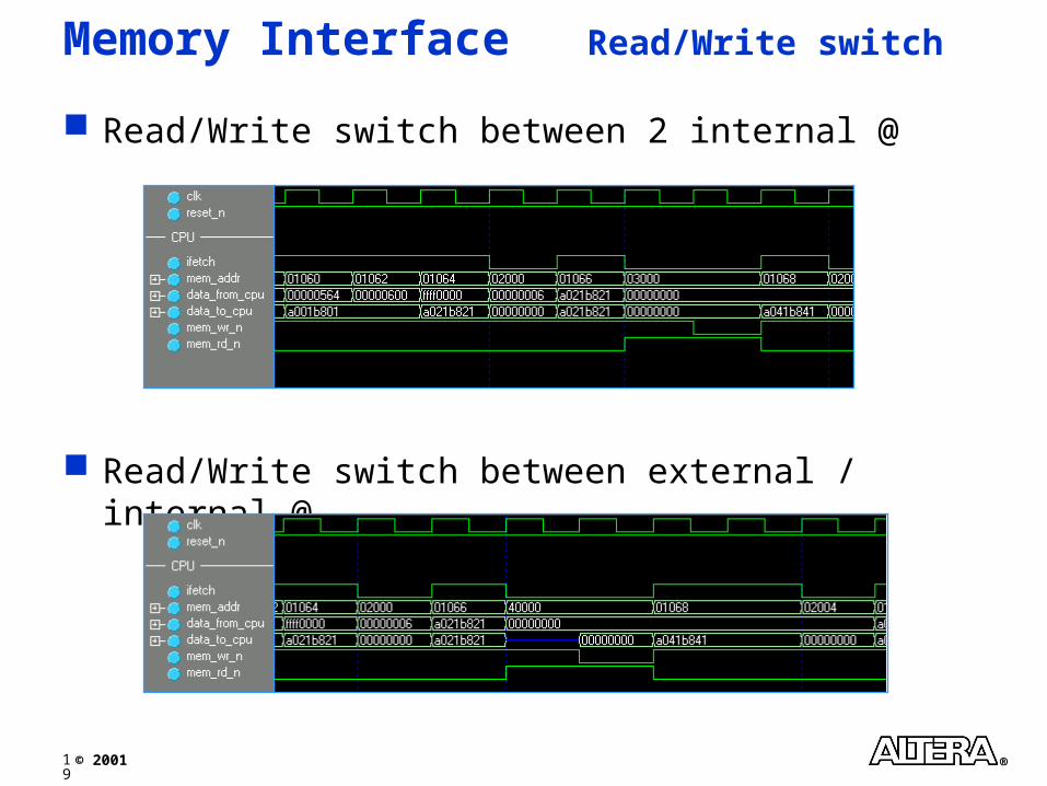
Memory Interface Read/Write switch
Read/Write switch between 2 internal @
Read/Write switch between external / internal @

20
© 2001 ®
Page transfert Tips 32bits
To support page transfert, do use:
– PFX
– LDP
– STP
ROM Program
RAM Datasource
RAM Datadest.
Instruction memory is connected to the Highest Bus.
21
© 2001 ®
Address @2Address @2
UpdateUpdate
Address @1Address @1
UpdateUpdate
Read cmdRead cmd
Write cmdWrite cmd
Address @2Address @2
ConstructionConstruction
Address @1Address @1
ConstructionConstruction
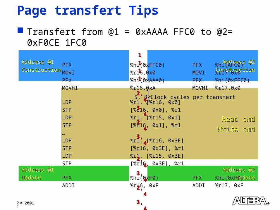
Page transfert Tips
Transfert from @1 = 0xAAAA FFC0 to @2= 0xF0CE 1FC0
PFX %hi(0xFFC0) PFX %hi(AFC0)
MOVI %r16,0x0 MOVI %r17,0x0
PFX %hi(0xAAA0) PFX %hi(0xFFC0)
MOVHI %r16,0xA MOVHI %r17,0x0
LDP %r1, [%r16, 0x0]
STP [%r16, 0x0], %r1
LDP %r1, [%r15, 0x1]
STP [%r16, 0x1], %r1
…
LDP %r1, [%r16, 0x3E]
STP [%r16, 0x3E], %r1
LDP %r1, [%r15, 0x3E]
STP [%r16, 0x3E], %r1
PFX %hi(0xF0) PFX %hi(0xF0)
ADDI %r16, 0xF ADDI %r17, 0xF
11
11
11
11
2, 42, 4
3, 43, 4
2, 42, 4
3, 43, 4
2, 42, 4
3, 43, 4
2, 42, 4
3, 43, 4
11
11
5, 8 Clock cycles per transfert

22
© 2001 ®
Page transfert Tips
Address @1 & @2 ConstructionAddress @1 & @2 Construction 88
64 Transferts64 Transferts 320/576320/576
Address @1 & @2 updateAddress @1 & @2 update 44
324/580 Clock cycles per 128 words access
ThroughputThroughput 80Mbytes/s, 80Mbytes/s, in the best case, if the memory instruction = data memory(Core running at 50MHz)
If data memory /= instruction memory then, Throughput 45Mbytes/s(Core running at 50MHz)

23
© 2001 ®
Compiler Aspect The C Code
Basic Loop declaration
void main(void)
{
volatile long *segment_read =(long *) 0x2000;
volatile long *segment_write =(long *) 0x2500;
for (i=0; i<100; i++)
{
segment_write[i] = *segment_read;
}
}

24
© 2001 ®
@destination update@destination update
Loop indexLoop index
Data StoringData Storing
Data LoadingData Loading
Loop testLoop test
Compiler Aspect Default Compiler's output
for (i= 0; i < 100; i++)
101a: 03 98 pfx %hi(0x60)
101c: 82 34 movi %g2,0x4
{
segment_write[i] = (*segment_read);
101e: 01 b0 ldp %g1,[%l0,0x0]
1020: 01 a8 stp [%l2,0x0],%g1
1022: ff 9f pfx %hi(0xffe0)
1024: e1 37 movi %g1,0x1f
1026: ff 9f pfx %hi(0xffe0)
1028: e1 6f movhi %g1,0x1f
102a: 22 00 add %g2,%g1
102c: c2 7e skprz %g2
102e: f7 87 br 101e <main+0xe>
1030: 92 04 addi %l2,0x4
}
25
© 2001 ®
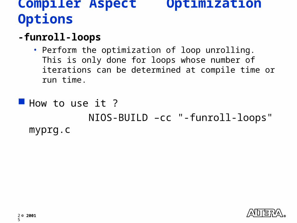
Compiler Aspect Optimization Options
-funroll-loops• Perform the optimization of loop unrolling. This is only done for loops
whose number of iterations can be determined at compile time or run time.
How to use it ?
NIOS-BUILD –cc "-funroll-loops" myprg.c

26
© 2001 ®
@destination update@destination update
Block Copy Block Copy
Block Copy Block Copy
Loop testLoop test
Compiler Aspect Optimization Options
Result
…
segment_write[i] = *segment_read;
101e: 01 b4 ldp %g1,[%l1,0x0]
1020: 01 a0 stp [%l0,0x0],%g1
1022: 90 04 addi %l0,0x4
1024: 01 b4 ldp %g1,[%l1,0x0]
1026: 01 a0 stp [%l0,0x0],%g1
1028: 90 04 addi %l0,0x4
102a: 01 b4 ldp %g1,[%l1,0x0]
102c: 01 a0 stp [%l0,0x0],%g1
102e: 90 04 addi %l0,0x4
…
1054: 01 b4 ldp %g1,[%l1,0x0]
1056: 01 a0 stp [%l0,0x0],%g1
1058: ff 9f pfx %hi(0xffe0)
105a: c1 36 movi %g1,0x16
105c: ff 9f pfx %hi(0xffe0)
105e: e1 6f movhi %g1,0x1f
1060: 22 00 add %g2,%g1
1062: c2 7e skprz %g2
1064: dc 87 br 101e <main+0xe>
1066: 90 04 addi %l0,0x4
Block Copy Block Copy
Block Copy Block Copy
10 times

27
© 2001 ®
C writing Aspect Nios_map.h & Nios_peripherals.h
Nios_map.h & Nios_peripherals.h are generated directly by the megawizard in the /mynios_sdk/inc directory.
How to use it in my C code ?
#define na_null ((void *) 0x00000000)
#define na_mycpu_cpu ((void *) 0x00000000)
#define na_mycpu_cpu_end ((void *) 0x00400000)
#define na_rom_boot ((void *) 0x00000000)
#define na_ram_sys ((void *) 0x00000400)
#define na_ram_prg ((void *) 0x00001000)
#define na_uart ((np_uart *) 0x00000800)
#define na_uart_irq 20
#define na_timer ((np_timer *) 0x00000600)
#define na_timer_irq 18
#define na_internal_ram_page_A ((void *) 0x00002000)
Nios_map.h
// Timer Registerstypedef volatile struct
{int np_timerstatus; // read only, 2 bits (any write to clear TO)int np_timercontrol; // write/readable, 4 bitsint np_timerperiodl; // write/readable, 16 bits
…int np_timersnaph; // read only, 16 bits} np_timer;
// Timer Register Bitsenum
{np_timerstatus_run_bit = 1, // timer is runningnp_timerstatus_to_bit = 0, // timer has timed outnp_timercontrol_stop_bit = 3, // stop the timer
…np_timercontrol_start_mask = (1<<2), // start the timernp_timercontrol_cont_mask = (1<<1), // continous modenp_timercontrol_ito_mask = (1<<0) // enable time out interrupt};
// Timer Routinesint nr_timer_milliseconds(void); // Starts on first call, hogs timer1.
Nios_peripherals.h

28
© 2001 ®
C writing Aspect Nios_map.h & Nios_peripherals.h
int main(void) {
np_timer *timer = na_timer;
long timerPeriod = 0xFFFFFFFF;
// Set Timer
timer->np_timerperiodh = timerPeriod >> 16; // Timer TimeOut Period
timer->np_timerperiodl = timerPeriod & 0xffff;
timer->np_timercontrol = timer->np_timercontrol
| np_timercontrol_cont_mask; // Set Continuous mode
timer->np_timercontrol = timer->np_timercontrol
& ~np_timercontrol_ito_mask; // IRQ Disabled
…
Pointer created Here !
Internal Timer Register selected Here !
Bit register selected Here !
30
© 2001 ®
Tuesday, 19 June 2001Tuesday, 19 June 2001
NiosTM Advanced Training
SESSION IISESSION II
Lab – Memory Accesses Measure

31
© 2001 ®
Goals
Creating a Quartus II project
Generating a NiosTM System Variation
Writing, compiling C code application to support Page transfers in different modesTemplate will be provided
Simulating with Modelsim (verilog mode)
Compiling w/ Quartus IIPin-Out file will be provided
Configuring the Nios board
Downloading SREC and Measure the access time
Using the GDB debugger
32
© 2001 ®
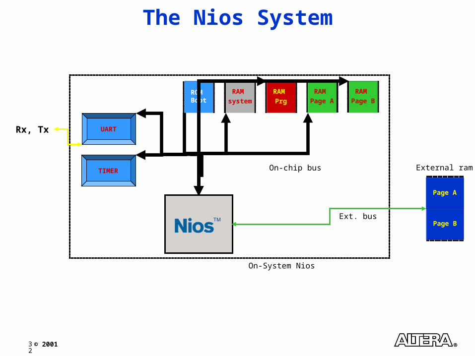
The Nios System
ROM Boot
Page B
RAM
system
UART
TIMER On-chip bus
Ext. bus
Rx, Tx
On-System Nios
RAM
Prg
RAM
Page A
RAM
Page B
Page A
External ram
33
© 2001 ®
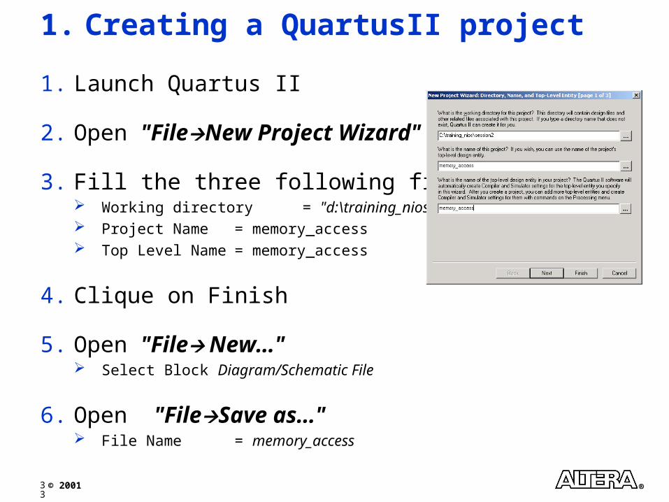
1. Creating a QuartusII project
1. Launch Quartus II
2. Open "FileNew Project Wizard"
3. Fill the three following fields Working directory = "d:\training_nios\session2" Project Name = memory_access Top Level Name = memory_access
4. Clique on Finish
5. Open "File New…" Select Block Diagram/Schematic File
6. Open "FileSave as…" File Name = memory_access

34
© 2001 ®
2. Generating a Nios System Variation 1/2
1. Launch the Nios Megawizard Plug-In Manager Double click in the Schematic Window Clique on the "MegaWizard Plug-In Manager…" button Select "Create a new custom megafunction variation" Select ALTERA Excalibur NiosTM megafunction Select Verilog HDL output type Give it the name mycpu
2. Do parameterise your core system NIOS 32bits, 20bits @, 256 files reg., 3bits shifter, No MSTEP, No MUL
Name Type Configuration Address #IRQ
rom_boot On-chip Rom 1K 32bits 0x0000 Use GERMS as contentsram_sys On_chip Ram 512 Words 32bits 0x0400 Leave blankram_prg On-chip Ram 3K 32bits 0x1000 Leave blanktimer Interval Timer 0x0600 18uart UART (RS232) 0x0800 20internal_ram_page_A On-chip Ram 1K 32bits 0x2000internal_ram_page_B On-chip Ram 1K 32bits 0x3000external_ram 0x4000032bits SRAM (256Kbytes in two IDT71V6)

35
© 2001 ®
2. Generating a Nios System Variation 2/2
3. Nios system organisation Main Prog Memory = ram_prg Main Data Memory = ram_sys Host Communication = uart Debug Communication = uart Boot ID Message = Free to fill Boot Device = ram_prg
For the simulation we will boot on the ram_prg which will be precharged.For real use, in the board, we will change the boot device to rom_germs
Interrupt Vector Table = ram_sys Synthesis Target Familly = None
For the simulation, we don't synthesis the core
4. Place the Nios system symbol in the schematic window
5. Save the schematic file as memory_access.bdf
"mycpu.ptf" file is generated which describes your whole Nios system

36
© 2001 ®
3. Writing & compiling a C Program
1. In Windows Explorer, create the directory mysrc inD:\training_nios\session2\mycpu_sdk\
2. Copy the mem_access.c file inD:\training_nios\session2\mycpu_sdk\mysrc\
3. Complete the program and set a transfert from Internal Page A, to External Page B.
4. Open a Bash Window & Go inD:\training_nios\session2\mycpu_sdk\mysrc\
5. Run "NIOS-BUILD mem_access.c" to generate compiled Code– mem_access.srec
– mem_access.objdump

37
© 2001 ®
4. PTF file modification
1. Open mycpu.ptf file with your Favorite Editor inD:\training_nios\session2\
2. Turn on simulation support file generation by setting variable do_build_sim to 1 as follows:
SYSTEM mycpu
{
WIZARD_SCRIPT_ARGUMENTS
{
do_build_sim = "1" ;
3. ram_prg user file specification Find the MODULE ram_prg section and Change the following lines
WIZARD_SCRIPT_ARGUMENTS
{
Writeable = "1";
Contents = "user_file";
Initfile = "mycpu_sdk\\mysrc\\mem_access.srec";
}

38
© 2001 ®
5. Generating the Simulation environment
1. Open a BASH window and go in "D:\training_nios\session2"
2. Run the following command GENERATE_PROJECT mycpu
3. Create a compile_verilog.do in "D:\training_nios\session2\mycpu_sim" Add vlog -work work ./mycpu_test_bench.v Add vsim work.mycpu_test_bench

39
© 2001 ®
6. Simulating with ModelSim 1/5
1. Launch Modelsim Altera-Edition or SE 5.4
2. Open "FileChange directory.." menu and select "D:\training_nios\session2\mycpu_sim"
3. Type "do compile_verilog.do" in the command line
4. Open the "ViewStructure" menu
5. Open the "ViewSignal" menu

40
© 2001 ®
6. Simulating with ModelSim 2/5
6. Select the following signals: /mycpu_test_bench/the_mycpu_core/clk /mycpu_test_bench/the_mycpu_core/reset_n /mycpu_test_bench/the_mycpu_core/the_timer/irq /mycpu_test_bench/the_mycpu_core/the_timer/timer_select /mycpu_test_bench/the_mycpu_core/the_timer/internal_counter [set the radix format to dec]
/mycpu_test_bench/the_mycpu_core/the_mycpu_cpu/ifetch /mycpu_test_bench/the_mycpu_core/the_mycpu_cpu/mem_addr [set the radix format to hex]
/mycpu_test_bench/the_mycpu_core/the_mycpu_cpu/data_from_cpu [set the radix format to hex]
/mycpu_test_bench/the_mycpu_core/the_mycpu_cpu/data_to_cpu [set the radix format to hex]
/mycpu_test_bench/the_mycpu_core/the_mycpu_cpu/mem_wr_n /mycpu_test_bench/the_mycpu_core/the_mycpu_cpu/mem_rd_n
7. In the Waves window, open "EditDisplay Properties…" Set to 1 the Signal Names path elements displayed
8. In the Waves window, Save your waves format as wave.do
9. Type "run 200µs" in the command line

41
© 2001 ®
6. Simulating with ModelSim 3/5
1. Find the beginning of the transfert Search for Value 0x2000 in the @ line
2. Count the number of clock cycles for the read access Nb_read = _______
3. Count the number of clock cycles for the write access Nb_write = _______
4. Find the @ or the instruction of the first read access and write access is fetched. How many clock cycles before the access is done ? Pipe_length = ______

42
© 2001 ®
6. Simulating with ModelSim 4/5
Re-Simulating each times the SW Has Been ModifiedRe-Simulating each times the SW Has Been Modified
1. Open a Bash Window & Go inD:\training_nios\session2\mycpu_sdk\mysrc\
2. Run "NIOS-BUILD mem_access.c" to generate compiled Code
3. Open a BASH window and go in "D:\training_nios\session2"
4. Run the following command GENERATE_PROJECT mycpu
5. Under ModelSim, in the command line Type "do compile_verilog.do"
Type "do wave.do"
Type "run 200 µs"
43
© 2001 ®
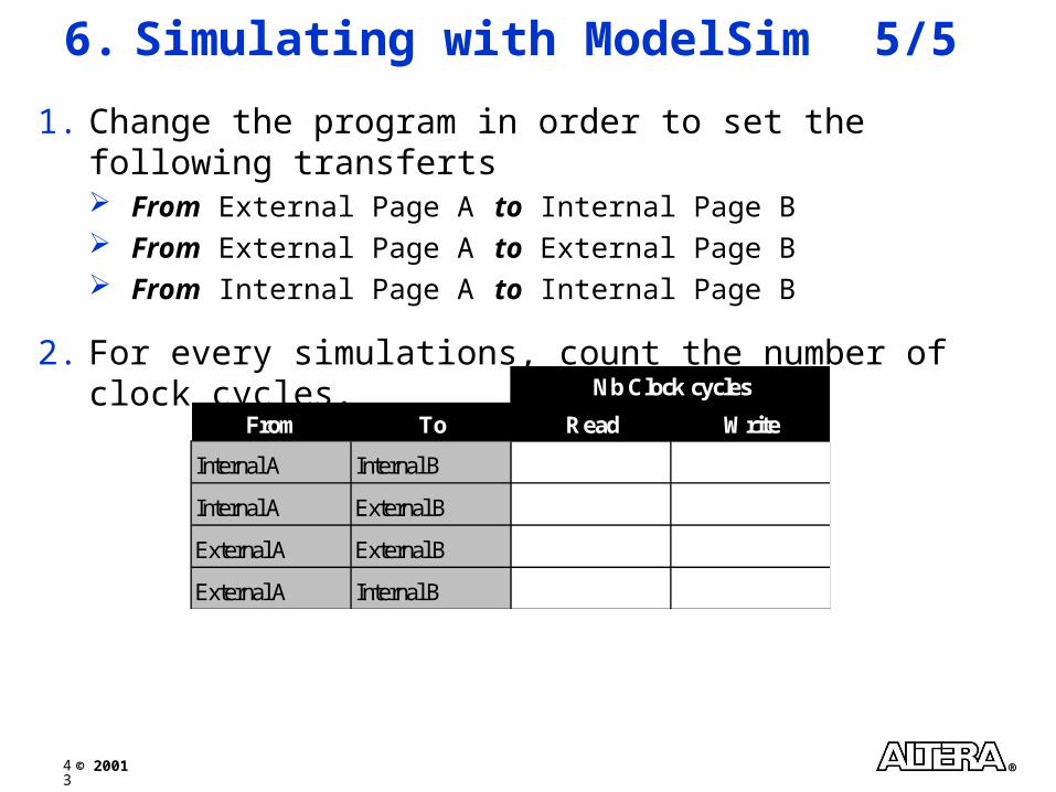
6. Simulating with ModelSim 5/5
1. Change the program in order to set the following transferts From External Page A to Internal Page B From External Page A to External Page B From Internal Page A to Internal Page B
2. For every simulations, count the number of clock cycles.
From To Read Write
Internal A Internal B
Internal A External B
External A External B
External A Internal B
Nb Clock cycles
44
© 2001 ®
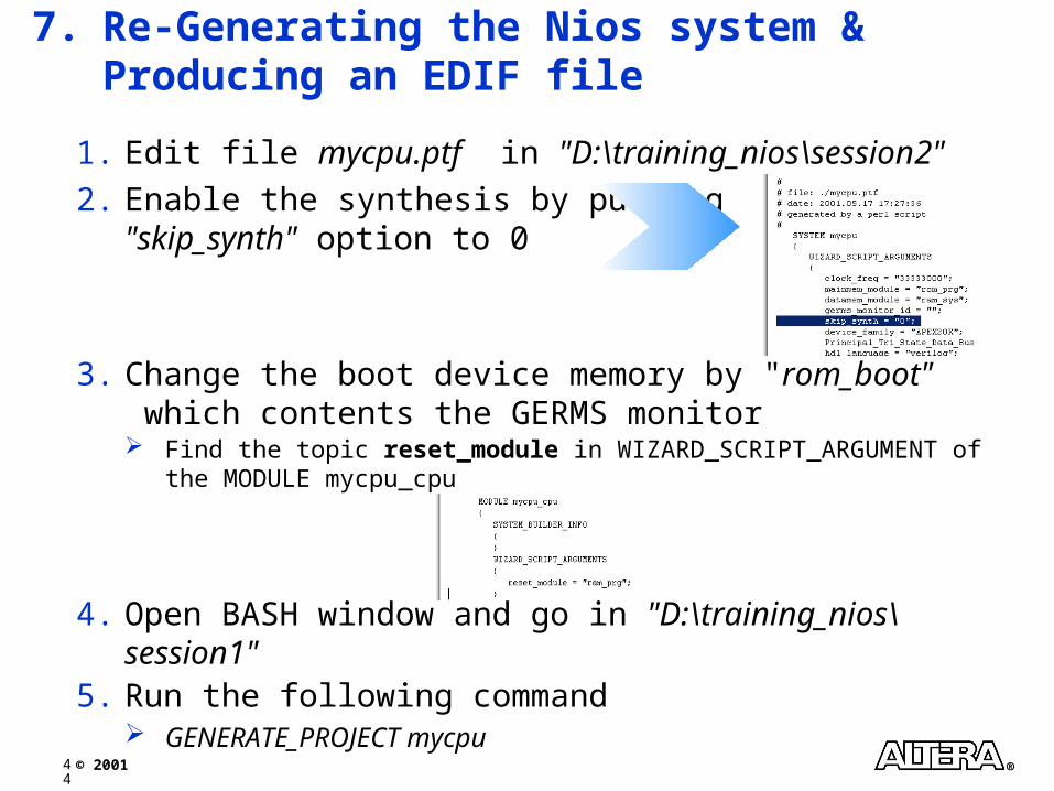
7. Re-Generating the Nios system & Producing an EDIF file
1. Edit file mycpu.ptf in "D:\training_nios\session2"
2. Enable the synthesis by putting "skip_synth" option to 0
3. Change the boot device memory by "rom_boot" which contents the GERMS monitor Find the topic reset_module in WIZARD_SCRIPT_ARGUMENT of the
MODULE mycpu_cpu
4. Open BASH window and go in "D:\training_nios\session1"5. Run the following command
GENERATE_PROJECT mycpu

45
© 2001 ®
8. Compiling w/ Quartus II 1/2
1. Under Quartus, double click in the schematic windowThe Symbol manager is launched
2. Type Input in the Name field and clique OK
3. Copy and past n times the Input symbol and connect all the input ports of the Nios symbol
4. Place a Output symbol in front of each output ports
5. Double Clique on each Input/Output symbol and change the name as shown hereafter

46
© 2001 ®
8. Compiling w/ Quartus II 2/2
1. Select the APEX device type Open "ProcessingCompiler Settings…" Select "Chips & Devices" tab Select Family APEX20KE and select EP20K200EFC484-2* Clique on "Device & Pin Options" button Select "Unused Pins" tab and select Reserve all unused pins
"As inputs, tri-stated" Clique OK 2 times.
2. Assign I/O pins accordingly to the Nios demo board features Close the project by selecting "fileClose Project" Under Windows Explorer open memory_access.csf file in "D:\
training_nios\session2" and copy the I/O assignment in the CHIP session from the session2_io_pin.txt file provided
* Please check on your board to know the exact 20K device mounted on it

47
© 2001 ®
9. Configuring the Nios board
1. Re-open the "memory_access" project The I/O assignments are now taken into account
2. Start the compilation by selecting "ProcessingStart compilation"
The compilation time takes about 6 minutesThe compilation time takes about 6 minutes
3. Open "ProcessingOpen Programmer" menu Clique "Add file" and select memory_access.sof file Enable "Program/Configure" box Start the configuration

48
© 2001 ®
10. Question ?
1. Why your application is running although you didn't send any SREC file through the UART by using Nios-Run ?
49
© 2001 ®
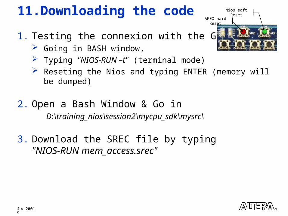
11. Downloading the code
1. Testing the connexion with the GERMS by Going in BASH window, Typing "NIOS-RUN –t" (terminal mode) Reseting the Nios and typing ENTER (memory will be dumped)
2. Open a Bash Window & Go inD:\training_nios\session2\mycpu_sdk\mysrc\
3. Download the SREC file by typing "NIOS-RUN mem_access.srec"
Nios soft Reset
APEX hard Reset

50
© 2001 ®
12. Measuring the throughput
1. Change the program in order to set the following transferts From Internal Page A to Internal Page B From Internal Page A to External Page B From External Page A to External Page B From External Page A to Internal Page B
2. For every simulations Note the number of clock cycles required to complet the loop, divide by the number of transfers done (32000), Multiple by 8 to get the throughput in bytes/s
From To Read Write
Internal A Internal B
Internal A External B
External A External B
External A Internal B
Throughput at 33MHz
51
© 2001 ®
13. Using of the debugger
1. Add Code to “main” Function#if NIOS_GDB
nios_gdb_install(1);
nios_gdb_breakpoint();
#endif
2. Build The Program nios-build -debug mem_access.c
3. Run The Shell Script Produced By “nios-build”myprogram.gdb
52
© 2001 ®
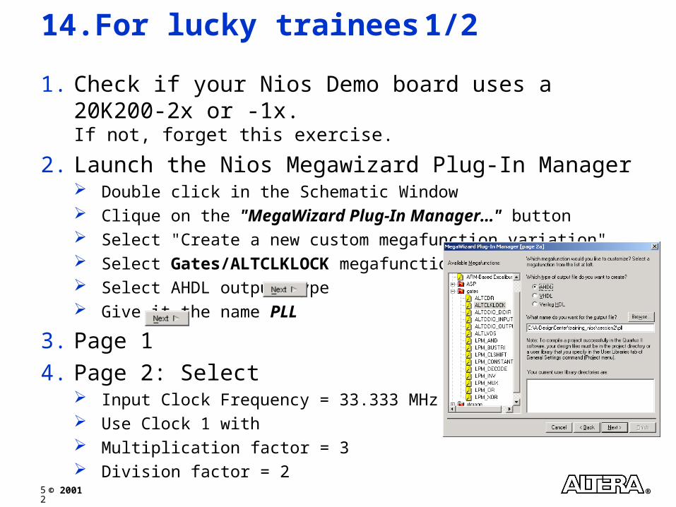
14. For lucky trainees 1/2
1. Check if your Nios Demo board uses a 20K200-2x or -1x. If not, forget this exercise.
2. Launch the Nios Megawizard Plug-In Manager Double click in the Schematic Window Clique on the "MegaWizard Plug-In Manager…" button Select "Create a new custom megafunction variation" Select Gates/ALTCLKLOCK megafunction Select AHDL output type Give it the name PLL
3. Page 1
4. Page 2: Select Input Clock Frequency = 33.333 MHz Use Clock 1 with Multiplication factor = 3 Division factor = 2

53
© 2001 ®
14. For lucky trainees 2/2
5. Place the PLL symbol as shown below
6. Double clique on the cpu symbol
7. Change the frequency to 33.333*1.5 = 49.9995 MHz
8. Generate the new variation
9. Configure the Nios Board with the new SOF file
10. Go back to step 11 and 12