© 2010 liang hu - ideals
TRANSCRIPT

© 2010 Liang Hu

SIZE EFFECTS ON SELF-ASSEMBLY AND MELTING OF SILVER-ALKANETHIOLATE ON INERT SURFACES
DISSERTATION
Submitted in partial fulfillment of the requirements for the degree of Doctor of Philosophy in Materials Science and Engineering
in the Graduate College of the University of Illinois at Urbana-Champaign, 2010
BY
LIANG HU
Urbana, Illinois
Doctoral Committee:
Associate Professor Leslie H. Allen, Chair, Director of Research Professor Phillip H. Geil Associate Professor Jian-Min Zuo Professor Kuang-Chien Hsieh

ii
ABSTRACT
Self-assembled materials produced in the reaction between alkanethiol and Ag are
characterized and compared. It is revealed that the size of the Ag substrate has a
significant role in the self-assembly process and determines the reaction products.
Alkanethiol adsorbs on the surface of Ag continuous planar thin films and only forms
self-assembled monolayers (SAMs), while the reaction between alkanethiol and Ag
clusters on inert surfaces is more aggressive and generates a significantly larger amount
of alkanethiolate. Two dissimilar products are yielded depending on the size of the
clusters. Small Ag clusters are more likely to be converted into multilayer silver-
alkanethiolate (AgSR, R = CnH2n+1) crystals, while larger Ag clusters form monolayer-
protected clusters (MPCs). The AgSR crystals are initially small and can ripen into large
lamellae during thermal annealing. The crystals have facets and flat terraces with
extended area, and have a strong preferred orientation in parallel with the substrate
surface. The MPCs move laterally upon annealing and reorganize into a single-layer
network with their separation distance approximately equal to the length of an extended
alkyl chain.
AgSR lamellar crystals grown on inert surfaces provide an excellent platform to
study the melting characteristics of crystalline lamellae of polymeric materials with the
thickness in the nanometer scale. This system is also unique in that each crystal has
integer number of layers – magic-number size (thickness). The size of the crystals is
controlled by adjusting the amount of Ag and the annealing temperature. X-ray
diffraction (XRD) and atomic force microscopy (AFM) are combined to accurately
determine the size (number of layers) of the lamellar crystals. The melting characteristics

iii
are measured with nanocalorimetry and show discrete melting transitions which are
attributed to the magic-number sizes of the lamellar crystals. The discrete melting
temperatures are intrinsic properties of the crystals with particular sizes. Smaller lamellar
crystals with less number of layers melt at lower temperatures. The melting point
depression is inversely proportional to the total thickness of the lamellae – the product of
the number of layers and the layer thickness.

iv
ACKNOWLEDGEMENTS
This work would not have been possible without the support of many people. I
gratefully thank my advisor, Prof. Les Allen, for guiding me on observing the world of
science, directing me on research, and always encouraging me to spread my wings. I am
also grateful to my committee members: Prof. Phillip Geil, Prof. Jian-Min Zuo and Prof.
Kuang-Chien Hsieh. They offered invaluable discussion and suggestion on my work.
Many thanks for the important experiences and kindly help from the group members: Dr.
Mikhail Efremov, Dr. Eric Olson, Dr. Ming Zhang, Dr. Zishu Zhang, Dr. Ravi
Kummamuru and Lito de la Rama. I would also like to thank Prof. Francois Schiettekatte
and Yonathan Anahory from the Université de Montréal in Canada for close
collaborations.
This work was supported by NSF-DMR-0735286. Microanalysis characterization
was carried out in part in the Frederick Seitz Materials Research Laboratory Central
Facilities, University of Illinois, which are partially supported by the U.S. Department of
Energy under grants DE-FG02-07ER46453 and DE-FG02-07ER46471. Thank the staffs
in MRL, especially Dr. Mauro Sardela, Dr. Changhui Lei, Dr. Jianguo Wen, Dr. Scott
MacLaren, Doug Jeffers, and Dr. Julio Soares, for their generous help. The
nanocalorimetry sensors and shadow masks were fabricated at the Cornell NanoScale
Facility, a member of the National Nanotechnology Infrastructure Network, which is
supported by the NSF-ECS-0335765.

v
TABLE OF CONTENTS
CHAPTER 1 INTRODUCTION ........................................................................................1
1.1 Self-assembled monolayers ..........................................................................1 1.2 Size effect on the self-assembly process.......................................................2 1.3 Metal-thiolate complexes..............................................................................4
1.3.1 Application.........................................................................................4 1.3.2 Molecular model of silver-alkanethiolate (AgSR).............................5 1.3.3 Comparison of AgSR, alkane and polyethylene ................................5 1.3.4 AgSR lamellar crystals grown on inert surfaces................................6
1.4 References.....................................................................................................7 1.5 Figures.........................................................................................................13
CHAPTER 2 SIZE-DEPENDENT MELTING: THEORIES AND MODELS ...............15
2.1 Metal clusters ..............................................................................................15 2.2 Polyethylene................................................................................................17 2.3 Alkane .........................................................................................................19 2.4 AgSR lamellar crystals ...............................................................................20 2.5 References...................................................................................................22 2.6 Figures.........................................................................................................26
CHAPTER 3 MEMS FABRICATION: NANOCALORIMETRY SENSOR AND
SELF-ALIGNED SHADOW MASK.........................................................28 3.1 Nanocalorimetry sensor ..............................................................................28
3.1.1 Introduction......................................................................................28 3.1.2 Fabrication .......................................................................................29 3.1.3 Calibration........................................................................................31 3.1.4 Calorimetric measurement ...............................................................32
3.2 Self-aligned shadow mask ..........................................................................33 3.2.1 Introduction......................................................................................33 3.2.2 Fabrication .......................................................................................35
3.3 References...................................................................................................36 3.4 Figures.........................................................................................................38
CHAPTER 4 SELF-ASSEMBLED MONOLAYERS OF HEXADECANETHIOL ON
SILVER THIN FILMS ...............................................................................41 4.1 Introduction.................................................................................................41 4.2 Experiment..................................................................................................43
4.2.1 Materials ......................................................................................43 4.2.2 Sample preparation ......................................................................43 4.2.3 Sample characterization ...............................................................44
4.2.3.1 Nanocalorimetry .........................................................44 4.2.3.2 Ellipsometry ...............................................................45 4.2.3.3 Other characterization techniques ..............................46
4.3 Melting transition........................................................................................46

vi
4.3.1 Mixed calorimetric signals of 2D SAMs and AgSR....................47 4.3.2 Calorimetric measurement of pure 2D SAMs .............................49
4.4 Thickness ....................................................................................................51 4.5 Conclusion ..................................................................................................51 4.6 References...................................................................................................52 4.7 Figures.........................................................................................................55
CHAPTER 5 SELF-ASSEMBLY OF SILVER-ALKANETHIOLATE LAMELLAR
CRYSTALS ON INERT SURFACES .......................................................58 5.1 Introduction.................................................................................................58 5.2 Experiment..................................................................................................59
5.2.1 Materials ......................................................................................59 5.2.2 Sample preparation ......................................................................60
5.2.2.1 Solution synthesis.......................................................61 5.2.2.2 Vapor synthesis ..........................................................62
5.2.3 Sample characterization ...............................................................62 5.2.3.1 Nanocalorimetry .........................................................63 5.2.3.2 Rutherford backscattering spectroscopy.....................63 5.2.3.3 Transmission electron microscopy .............................64 5.2.3.4 Atomic force microscopy ...........................................65 5.2.3.5 X-ray diffraction.........................................................65 5.2.3.6 Scanning electron microscopy....................................66 5.2.3.7 Fourier transform infrared spectroscopy ....................66
5.3 Reaction with alkanethiol: Ag thin films vs. Ag clusters ..........................66 5.4 Amount .......................................................................................................68 5.5 Morphology.................................................................................................70 5.6 Composition................................................................................................74 5.7 Multilayer structure.....................................................................................76 5.8 In-plane ordering.........................................................................................78 5.9 Crystal texture.............................................................................................79 5.10 Degradation of AgSR upon e-beam irradiation ..........................................80 5.11 Reaction mechanism ...................................................................................81 5.12 Transport of MPCs......................................................................................83 5.13 Conclusion ..................................................................................................85 5.14 References...................................................................................................86 5.15 Figures and tables .......................................................................................90
CHAPTER 6 SIZE OF SILVER-ALKANETHIOLATE LAMELLAR CRYSTALS...102
6.1 Introduction...............................................................................................102 6.2 Size Measurement.....................................................................................103
6.2.1 X-ray diffraction ........................................................................103 6.2.2 X-ray reflectivity........................................................................103 6.2.3 Atomic force microscopy...........................................................104
6.2.3.1 Direct measurement of crystal size...........................104 6.2.3.2 Size distribution........................................................104 6.2.3.3 Data correction .........................................................106

vii
6.2.3.4 Amount of AgSR......................................................107 6.3 Size control ...............................................................................................108
6.3.1 Amount of Ag ............................................................................108 6.3.2 Annealing temperature...............................................................110
6.4 Small AgSR crystals .................................................................................111 6.4.1 Mono-dispersed 2-layer AgSC10 crystals .................................111
6.4.1.1 Crystal structure........................................................111 6.4.1.2 Crystal size ...............................................................112
6.4.2 Mono-dispersed 1-layer AgSC10 crystals .................................113 6.4.2.1 Crystal structure........................................................113 6.4.2.2 Crystal size ...............................................................114 6.4.2.3 Lateral dimension .....................................................115
6.5 Conclusion ................................................................................................116 6.6 References.................................................................................................117 6.7 Figures.......................................................................................................118
CHAPTER 7 SIZE-DEPENDENT MELTING OF SILVER-ALKANETHIOLATE
LAMELLAR CRYSTALS .......................................................................125 7.1 Melting characteristics of multilayer AgSR lamellar crystals ..................125
7.1.1 Melting characteristics of AgSC16............................................125 7.1.2 Comparison with alkane, polyethylene and AgSR bulk ............126
7.2 Discrete melting ........................................................................................127 7.3 Size-dependent melting-point depression .................................................129
7.3.1 Number of layers........................................................................129 7.3.2 Layer thickness ..........................................................................130 7.3.3 Lateral dimension.......................................................................131
7.4 Conclusion ................................................................................................131 7.5 References.................................................................................................131 7.6 Figures.......................................................................................................133
CHAPTER 8 SUMMARY AND FUTURE WORK ......................................................139
8.1 Summary ...................................................................................................139 8.2 Future work...............................................................................................140
8.2.1 Synthesis ....................................................................................140 8.2.2 Characterization .........................................................................141 8.2.3 Materials ....................................................................................141
8.3 References.................................................................................................142 8.4 Figures.......................................................................................................143
Appendix A DISCOVERY TIMELINE........................................................................144
Appendix B DEPOSITION CONTROL.......................................................................145
Appendix C STICKING COEFFICIENT OF SILVER ON SURFACES ....................148
Appendix D RBS MEASUREMENT ...........................................................................150

viii
Appendix E XRD ARTIFACT .....................................................................................151
Appendix F BASELINE CHANGE IN NANOCALORIMETRY...............................153
Appendix G REVERSIBILITY IN NANOCALORIMETRY......................................156

1
CHAPTER 1
INTRODUCTION
The self-assembly of organic materials on metals is a quickly developing field. In
the self-assembly process, the organic materials can spontaneously adsorb on metal
surfaces with an ordered arrangement, or form metal-organic complexes with an ordered
structure. This self-organizing process is largely due to the strong affinity between metals
and certain functional groups in the organic materials.[1, 2] The most extensively studied
systems are the self-assembly of organosulfur compounds such as alkanethiol
(CnH2n+1SH) on noble metals (Au, Ag, Cu, etc.).[3]
However, even for a binary system with one species of metal and one organic
material, there are several classes of self-assembled structures such as self-assembled
monolayers (SAMs) on extended metal surfaces, monolayer-protected clusters (MPCs)
and metal-thiolate complexes.[4, 5] Although the main components in these structures are
the same, the overall composition ratio of S/Ag and the synthesis method are much
different.
1.1. Self-assembled monolayers
The most studied self-assembly systems are self-assembled monolayers (SAMs)
grown on the surfaces of metal substrates. SAMs consist of ordered molecular structures
which form through the adsorption of a surfactant from solution or vapor phase onto a
solid surface.[1] There are many kinds of SAMs formed from different precursors, among
which alkanethiol is the most studied, due to its simplicity and easy preparation.[3] The
driving forces for the self-assembly process include the strong affinity between the
headgroup (-SH) and the metal substrate, and the van der Waals interaction between alkyl

2
chains.[1] Both interactions contribute to the arrangement in the self-assembled structures,
and also compete with each other.[6]
SAMs can form on different types of metal substrates, including planar surfaces
and clusters. Extended two-dimensional (2D) SAMs with ordered arrangement are
obtained when a planar metal surface (e.g. Au, Ag, Cu, etc.) is immersed into an
alkanethiol solution or is in contact with alkanethiol vapor.[1, 7-11] Different techniques
(diffraction, spectroscopy and microscopy) are used to study the structures of SAMs.[2]
For example, it is revealed that the unit cell of the alkanethiol SAMs on Au(111)
corresponds to a c(4 × 2) superlattice of a basic (√3x√3)R30° hexagonal lattice,[12-14]
while the organization of alkanethiol SAMs on Ag(111) corresponds to a (√7x√7)R10.9°
lattice.[15] However, the interfacial structures still remain controversial.[16] Recent
experimental and theoretical studies proposed new models (metal-thiolate complexes and
polymeric metal thiolate) about the interfacial structures.[17-20]
SAMs can also grow on the surface of metal clusters to form MPCs. Brust et al.
first reported the synthesis of thermally stable and air-stable alkanethiol-monolayer-
protected Au nanoparticles with controlled sizes. The nanoparticles are synthesized via
the reduction of HAuCl4 with NaBH4 in the presence of alkanethiol.[21, 22] MPCs can
also be synthesized with an aerosol processing approach.[23] MPCs can further organize
into a three-dimensional (3D) or two-dimensional (2D) superlattice.[23-26]
1.2. Size effect on the self-assembly process
The size of the metal substrates is important to the nature of the monolayers, since
it determines the kinetic and thermodynamic stability of the thiolate systems.

3
First, SAMs act as a kinetic barrier on the substrate surface. In the 2D SAMs on
planar metal substrate, the overall composition ratio (S/Metal) approaches zero since only
the metal surface reacts with alkanethiol and monolayers form on the surface. This
reaction/adsorption is self-limiting, since the formed SAMs act as a protective barrier and
prevents further reaction between alkanethiol and the underlying metal. Similarly, SAMs
coated on metal clusters can protect and stabilize the nanoparticles .[27]
However, there are exceptions to the protective effect of SAMs. Surface pitting
has been observed on planar Au and Ag substrates during the adsorption of alkanethiol,
together with transport of metal atoms from the surface to the solution.[28-30] For SAMs
grown on planar Ag substrates which are immersed in alkanethiol solution for a long
time, the adsorbed layer shows unexpected large thickness.[1, 8] In addition, multilayer
alkanethiolate can form on liquid Hg.[3]
This self-protection effect is further weakened for SAMs in MPCs. MPCs have an
intermediate composition ratio: 0 < S/Metal <1. The size distribution and S/Metal ratio of
MPCs can be systematically varied. For example, MPCs with poly-dispersed sizes can be
transformed into a nearly mono-dispersed distribution when they are refluxed in the
presence of excess alkanethiol.[31-33] The surface curvature which is dependent on the
cluster size plays an important role in the self-assembly process and affects the self-
protection effect of SAMs during the reaction.
Second, it is reported that only discrete sizes of MPCs have been observed.[34,
35] This phenomenon has been explained with “noble-gas superatom” model.[25, 36, 37]
The MPC is considered as a metallic core with a metal-thiolate complex shell. The metal
atoms in the core are still in the metallic state and maintain bulk structure, whereas those

4
in the shell are bonded with organic ligands and are oxidized. A stable MPC satisfies
three requirements: (1) a compact, symmetric metal core; (2) electron shell closing in the
metal core; (3) complete steric shielding of the ligand shell. Therefore, only the MPCs
with some certain sizes (magic-number sizes) are electronically and geometrically stable.
If the sizes of the metal clusters are large, the properties of the MPCs approach
those of 2D SAMs. If the size of the metallic core is reduced to some lower limit, then all
of the metal atoms in the cluster is directly bonded to S.[5, 38] However, for long-chain
ligands, in the case where stoichiometry is 1.0, alternative structures to MPCs may be
thermodynamically favorable such as polymeric metal-thiolate complexes.
1.3. Metal-thiolate complexes
In contrast to the monolayer structure of SAMs, metal-thiolate complexes (metal
= Au, Ag, Cu, etc.) have multilayer structure with each layer registered to one
another.[39-46] Metal-thiolate complexes are important in the synthesis of nanoparticles
(MPCs) since it is an intermediate product during the reaction.[47, 48]
1.3.1 Application
Metal-thiolate complexes have potential application in many fields. It is
discovered that metal-alkanethiolate can transform into nanoparticles upon electron beam
irradiation, which makes it a potential material for electron beam writing.[49, 50] Recent
studies also show metal-thiolate complexes have interesting luminescence properties.[51,
52] Luminescence of metal complexes have been an interesting topic in the research
fields such as photoactive reagent,[53] light-emitting diode,[54] and sensors for volatile
organic compounds.[55]

5
1.3.2 Molecular model of silver-alkanethiolate (AgSR)
Among the metal-thiolate complexes, the polymeric silver-alkanethiolate (AgSR,
R = CnH2n+1) has been synthesized through the reaction between silver nitrate (AgNO3)
and alkanethiol in solution.[39, 40, 42] The composition ratio of S/Ag in AgSR phase is
determined to be 1.0 which indicates the ratio of alknethiolate to Ag is also 1.0.[42] The
structure of AgSR has been characterized by several research groups.[39-46] Dance et al.
first proposed a multilayer structure (Figure 1.1(a)) for the AgSR crystals.[39] Each
AgSR layer (Figure 1.1(b)) has a planar polymeric structure of –(Ag-S)– network (Figure
1.1(c)) as the central plane (backbone). Fully extended alkyl chains are bonded to S and
extend on both sides of the central plane.[42] It is also found that the chains are tilted for
about 13º from the normal direction of the central plane.[42] The arrangement of the
alkyl chains in AgSR is analogous to that in 2D SAMs on a planar substrate.[42]
1.3.3 Comparison of AgSR, alkane and polyethylene
The physical properties of AgSR crystals are analogous to alkane and
polyethylene crystals, since the main components of these three materials are
hydrocarbon chains (alkyl chains). The hydrocarbon chains are packed in ordered
arrangements because of the chain-chain interactions induced by van der Waals forces.
Disordering of hydrocarbon chains is the main contribution to the melting
enthalpy. Therefore, the heat of fusion per repeating unit (Hf_C) is comparable among
these materials, but increases slightly with the chain length. Figure 1.2(a) compares Hf_C
of bulk AgSR with that of n-alkane and polyethylene (assuming 100% crystallinity).[56]
To simplify the comparison, the repeating unit includes methylene group (CH2) and

6
methyl group (CH3) which are treated as equivalent here. Polyethylene has the largest
Hf_C, while Hf_C of bulk AgSR is close to that of alkane.
On the other hand, the melting point (Tm) of AgSR is much higher than that of
alkane, as shown in Figure 1.2(b). For example, Voicu et al. reported that bulk AgSC16
crystals melt at 133.5 ºC,[43] while n-hexadecane (C16H22) melts at 18.2 ºC,[56] although
they have same chain length. This is because AgSR has an additional restriction from the
central plane –(Ag-S)– which further limits the movement of alkyl chains. It should be
noted that the melt phase of AgSR discussed here is not a liquid phase as alkane melt, but
a lamellar (smectic-A) or a micellar liquid crystal structure.[40, 42] Therefore, the
entropy change in the melting of AgSR is lower than that of alkane (Figure 1.2(c)),
although the enthalpy change is close.[57] Since Tm = ΔH/ΔS, it explains the higher
melting point of AgSR compared to alkane. In fact, the melting point of bulk AgSR is
close to that of polyethylene. The melting point of polyethylene depends on the
crystallinity and lamellar thickness. For single-crystal lamellae of polyethylene, the
equilibrium melting point is calculated to be 141 ºC.[58] AgSR is also considered a
polymeric material, as the central plane of –(Ag-S)– inside each layer forms a polymeric
network.[40, 44, 47, 59]
1.3.4 AgSR lamellar crystals grown on inert surfaces
In this work, a new synthesis method is introduced which employs the reaction
between alkanethiol and nanometer-sized Ag clusters prepared on inert substrates. The
obtained reaction products include AgSR lamellar crystals and MPCs. This method is
similar to the preparation of 2D SAMs, except that the planar metal substrate is replaced
with Ag clusters. The small size of Ag clusters weakens the self-protective effect of

7
SAMs and allows the formation and co-existence of both MPCs and AgSR lamellar
crystals.
The advantage of this method is that the crystal size (number of layers) of the
synthesized AgSR lamellae can be adjusted by tuning the amount of Ag on the surface
and the annealing temperature. Therefore, AgSR lamellar crystals provide a platform for
studying the change of the properties as a function of size. Furthermore, the synthesized
AgSR lamellar crystals are oriented with the substrate surface which makes it easier to
accurately measure the size of the crystals.
1.4. References
1. Love, J. C., Estroff, L. A., Kriebel, J. K., Nuzzo, R. G., Whitesides, G. M., Self-assembled monolayers of thiolates on metals as a form of nanotechnology. Chemical Reviews, 105, 1103-1169 (2005).
2. Schreiber, F., Structure and growth of self-assembling monolayers. Progress in
Surface Science, 65, 151 (2000). 3. Ulman, A., Thin Films. Vol. 24, Self-Assembled Monolayers of Thiols. Academic
Press: San Diego, CA, 1998. 4. Whetten, R. L., Price, R. C., Nano-golden order. Science, 318, 407-408 (2007). 5. Negishi, Y., Nobusada, K., Tsukuda, T., Glutathione-protected gold clusters
revisited: Bridging the gap between gold(I)-thiolate complexes and thiolate-protected gold nanocrystals. Journal of the American Chemical Society, 127, 5261-5270 (2005).
6. Cossaro, A., Mazzarello, R., Rousseau, R., Casalis, L., Verdini, A., Kohlmeyer,
A., Floreano, L., Scandolo, S., Morgante, A., Klein, M. L., Scoles, G., X-ray diffraction and computation yield the structure of alkanethiols on gold(111). Science, 321, 943-946 (2008).
7. Bain, C. D., Troughton, E. B., Tao, Y., Evall, J., Whitesides, G. M., Nuzzo, R. G.,
Formation of monolayer films by the spontaneous assembly of organic thiols from solution onto gold. Journal of the American Chemical Society, 111, 321-335 (1989).

8
8. Laibinis, P. E., Whitesides, G. M., Allara, D. L., Tao, Y. T., Parikh, A. N., Nuzzo, R. G., Comparison of the structures and wetting properties of self-assembled monolayers of n-alkanethiols on the coinage metal surfaces, copper, silver, and gold. Journal of the American Chemical Society, 113, 7152-7167 (1991).
9. Walczak, M. M., Chung, C. K., Stole, S. M., Widrig, C. A., Porter, M. D.,
Structure and Interfacial Properties of Spontaneously Adsorbed Normal-Alkanethiolate Monolayers on Evaporated Silver Surfaces. Journal of the American Chemical Society, 113, 2370-2378 (1991).
10. Poirier, G. E., Pylant, E. D., The self-assembly mechanism of alkanethiols on
Au(111). Science, 272, 1145-1148 (1996). 11. Schreiber, F., Eberhardt, A., Leung, T. Y. B., Schwartz, P., Wetterer, S. M.,
Lavrich, D. J., Berman, L., Fenter, P., Eisenberger, P., Scoles, G., Adsorption mechanisms, structures, and growth regimes of an archetypal self-assembling system: Decanethiol on Au(111). Physical Review B, 57, 12476-12481 (1998).
12. Schreiber, F., Structure and growth of self-assembling monolayers. Progress in
Surface Science, 65, 151-257 (2000). 13. Widrig, C. A., Alves, C. A., Porter, M. D., Scanning tunneling microscopy of
ethanethiolate and n-octadecanethiolate monolayers spontaneously absorbed at gold surfaces. J. Am. Chem. Soc., 113, 2805-2810 (1991).
14. Poirier, G. E., Tarlov, M. J., The c(4X2) Superlattice of n-Alkanethiol Monolayers
Self-Assembled on Au(111). Langmuir, 10, 2853-2856 (1994). 15. Fenter, P., In Self-Assembled Monolayers of Thiols, Ulman, A., Ed., Academic
Press: San Diego, CA, 1998, p 128. 16. Woodruff, D. P., The interface structure of n-alkylthiolate self-assembled
monolayers on coinage metal surfaces. Physical Chemistry Chemical Physics, 10, 7211-7221 (2008).
17. Yu, M., Bovet, N., Satterley, C. J., Bengio, S., Lovelock, K. R. J., Milligan, P. K.,
Jones, R. G., Woodruff, D. P., Dhanak, V., True nature of an archetypal self-assembly system: Mobile Au-thiolate species on Au(111). Physical Review Letters, 97, (2006).
18. Gronbeck, H., Hakkinen, H., Polymerization at the alkylthiolate-Au(111)
interface. Journal of Physical Chemistry B, 111, 3325-3327 (2007). 19. Gronbeck, H., Hakkinen, H., Whetten, R. L., Gold-Thiolate Complexes Form a
Unique c(4 x 2) Structure on Au(111). Journal of Physical Chemistry C, 112, 15940-15942 (2008).

9
20. Mazzarello, R., Cossaro, A., Verdini, A., Rousseau, R., Casalis, L., Danisman, M.
F., Floreano, L., Scandolo, S., Morgante, A., Scoles, G., Structure of a CH3S monolayer on Au(111) solved by the interplay between molecular dynamics calculations and diffraction measurements. Physical Review Letters, 98, (2007).
21. Brust, M., Walker, M., Bethell, D., Schiffrin, D. J., Whyman, R., Synthesis of
Thiol-Derivatized Gold Nanoparticles in a 2-Phase Liquid-Liquid System. Journal of the Chemical Society-Chemical Communications, 801-802 (1994).
22. Heath, J. R., Knobler, C. M., Leff, D. V., Pressure/temperature phase diagrams
and superlattices of organically functionalized metal nanocrystal monolayers: The influence of particle size, size distribution, and surface passivant. Journal of Physical Chemistry B, 101, 189-197 (1997).
23. Harfenist, S. A., Wang, Z. L., Alvarez, M. M., Vezmar, I., Whetten, R. L., Highly
oriented molecular Ag nanocrystal arrays. Journal of Physical Chemistry, 100, 13904-13910 (1996).
24. Whetten, R. L., Khoury, J. T., Alvarez, M. M., Murthy, S., Vezmar, I., Wang, Z.
L., Stephens, P. W., Cleveland, C. L., Luedtke, W. D., Landman, U., Nanocrystal gold molecules. Adv. Mater., 8, 428-& (1996).
25. Jadzinsky, P. D., Calero, G., Ackerson, C. J., Bushnell, D. A., Kornberg, R. D.,
Structure of a thiol monolayer-protected gold nanoparticle at 1.1 angstrom resolution. Science, 318, 430-433 (2007).
26. Sandhyarani, N., Resmi, M. R., Unnikrishnan, R., Vidyasagar, K., Ma, S. G.,
Antony, M. P., Selvam, G. P., Visalakshi, V., Chandrakumar, N., Pandian, K., Tao, Y. T., Pradeep, T., Monolayer-protected cluster superlattices: Structural, spectroscopic, calorimetric, and conductivity studies. Chemistry of Materials, 12, 104-113 (2000).
27. Brust, M., Walker, M., Bethell, D., Schiffrin, D. J., Whyman, R., Synthesis of
thiol-derivatised gold nanoparticles in a two-phase liquid-liquid system. J. Chem. Soc. Chem. Commun., 7, 801-802 (1994).
28. Schonenberger, C., Sondag-Huethorst, J. A. M., Jorritsma, J., Fokkink, L. G. J.,
What Are the "Holes" in Self-Assembled Monolayers of Alkanethiols on Gold? Langmuir, 10, 611-614 (1994).
29. Sondaghuethorst, J. A. M., Schonenberger, C., Fokkink, L. G. J., Formation of
Holes in Alkanethiol Monolayers on Gold. Journal of Physical Chemistry, 98, 6826-6834 (1994).

10
30. Dhirani, A., Hines, M. A., Fisher, A. J., Ismail, O., Guyotsionnest, P., Structure of Self-Assembled Decanethiol on Ag(111) - a Molecular Resolution Scanning-Tunneling-Microscopy Study. Langmuir, 11, 2609-2614 (1995).
31. Lin, X. M., Sorensen, S. M., Klabunde, K. J., Digestive Ripening, Nanophase
Segregation and Superlattice Formation in Gold Nanocrystal Colloids. Journal of Nanoparticle Research, 2, 157-164 (2000).
32. Prasad, B. L. V., Stoeva, S. I., Sorensen, C. M., Klabunde, K. J., Digestive
ripening of thiolated gold nanoparticles: The effect of alkyl chain length. Langmuir, 18, 7515-7520 (2002).
33. Smetana, A. B., Klabunde, K. J., Sorensen, C. M., Synthesis of spherical silver
nanoparticles by digestive ripening, stabilization with various agents, and their 3-D and 2-D superlattice formation. Journal of Colloid and Interface Science, 284, 521-526 (2005).
34. Whetten, R. L., Khoury, J. T., Alvarez, M. M., Murthy, S., Vezmar, I., Wang, Z.
L., Stephens, P. W., Cleveland, C. L., Luedtke, W. D., Landman, U., Nanocrystal gold molecules. Advanced Materials, 8, 428-& (1996).
35. Hostetler, M. J., Wingate, J. E., Zhong, C. J., Harris, J. E., Vachet, R. W., Clark,
M. R., Londono, J. D., Green, S. J., Stokes, J. J., Wignall, G. D., Glish, G. L., Porter, M. D., Evans, N. D., Murray, R. W., Alkanethiolate gold cluster molecules with core diameters from 1.5 to 5.2 nm: Core and monolayer properties as a function of core size. Langmuir, 14, 17-30 (1998).
36. Hakkinen, H., Walter, M., Gronbeck, H., Divide and protect: Capping gold
nanoclusters with molecular gold-thiolate rings. Journal of Physical Chemistry B, 110, 9927-9931 (2006).
37. Walter, M., Akola, J., Lopez-Acevedo, O., Jadzinsky, P. D., Calero, G., Ackerson,
C. J., Whetten, R. L., Gronbeck, H., Hakkinen, H., A unified view of ligand-protected gold clusters as superatom complexes. Proceedings of the National Academy of Sciences of the United States of America, 105, 9157-9162 (2008).
38. Gronbeck, H., Walter, M., Hakkinen, H., Theoretical characterization of cyclic
thiolated gold clusters. Journal of the American Chemical Society, 128, 10268-10275 (2006).
39. Dance, I. G., Fisher, K. J., Banda, R. M. H., Scudder, M. L., Layered Structure of
Crystalline AgSR. Inorganic Chemistry, 30, 183-187 (1991). 40. Baena, M. J., Espinet, P., Lequerica, M. C., Levelut, A. M., Mesogenic Behavior
of Silver Thiolates with Layered Structure in the Solid-State - Covalent Soaps. Journal of the American Chemical Society, 114, 4182-4185 (1992).

11
41. Fijolek, H. G., Grohal, J. R., Sample, J. L., Natan, M. J., A facile trans to gauche
conversion in layered silver butanethiolate. Inorganic Chemistry, 36, 622-628 (1997).
42. Bensebaa, F., Ellis, T. H., Kruus, E., Voicu, R., Zhou, Y., Characterization of
self-assembled bilayers: Silver-alkanethiolates. Langmuir, 14, 6579-6587 (1998). 43. Voicu, R., Badia, A., Morin, F., Lennox, R. B., Ellis, T. H., Thermal Behavior of
a Self-Assembled Silver n-Dodecanethiolate Layered Material Monitored by DSC, FTIR, and 13 C NMR Spectroscopy. Chemistry of Materials, 12, 2646-2652 (2000).
44. Voicu, R., Badia, A., Morin, F., Lennox, R. B., Ellis, T. H., Structure and
Dynamics of Selectively Deuterated Self-Assembled Silver n-Octadecanethiolate Layerered Materials. Chemistry of Materials, 13, 2266-2271 (2001).
45. Parikh, A. N., Gillmor, S. D., Beers, J. D., Beardmore, K. M., Cutts, R. W.,
Swanson, B. I., Characterization of chain molecular assemblies in long-chain, layered silver thiolates: A joint infrared spectroscopy and x-ray diffraction study. Journal of Physical Chemistry B, 103, 2850-2861 (1999).
46. Bardeau, J. F., Parikh, A. N., Beers, J. D., Swanson, B. I., Phase behavior of a
structurally constrained organic-inorganic crystal: Temperature-dependent infrared spectroscopy of silver n-dodecanethiolate. Journal of Physical Chemistry B, 104, 627-635 (2000).
47. Yee, C. K., Jordan, R., Ulman, A., White, H., King, A., Rafailovich, M., Sokolov,
J., Novel one-phase synthesis of thiol-fuctionalized gold, palladium, and iridium nanoparticles using superhydride. Langmuir, 15, 3486-3491 (1999).
48. Chen, S. W., Templeton, A. C., Murray, R. W., Monolayer-protected cluster
growth dynamics. Langmuir, 16, 3543-3548 (2000). 49. Corbierre, M. K., Beerens, J., Lennox, R. B., Gold nanoparticles generated by
electron beam lithography of gold(I)-thiolate thin films. Chemistry of Materials, 17, 5774-5779 (2005).
50. Kim, J. U., Cha, S. H., Shin, K., Jho, J. Y., Lee, J. C., Synthesis of gold
nanoparticles from gold(I)-alkanethiolate complexes with supramolecular structures through electron beam irradiation in TEM. Journal of the American Chemical Society, 127, 9962-9963 (2005).
51. Bachman, R. E., Bodolosky-Bettis, S. A., Glennon, S. C., Sirchio, S. A.,
Formation of a novel luminescent form of Gold(I) phenylthiolate via self-assembly

12
and decomposition of isonitrilegold(I) phenylthiolate complexes. Journal of the American Chemical Society, 122, 7146-7147 (2000).
52. Cha, S. H., Kim, J. U., Kim, K. H., Lee, J. C., Preparation and photoluminescent
properties of gold(I)-alkanethiolate complexes having highly ordered supramolecular structures. Chemistry of Materials, 19, 6297-6303 (2007).
53. Yam, V. W. W., Lo, K. K. W., Luminescent polynuclear d(10) metal complexes.
Chemical Society Reviews, 28, 323-334 (1999). 54. Ma, Y. G., Che, C. M., Chao, H. Y., Zhou, X. M., Chan, W. H., Shen, J. C., High
luminescence gold(I) and copper(I) complexes with a triplet excited state for use in light-emitting diodes. Advanced Materials, 11, 852-857 (1999).
55. Fernandez, E. J., Lopez-de-Luzuriaga, J. M., Monge, M., Olmos, M. E., Perez, J.,
Laguna, A., Mohamed, A. A., Fackler, J. P., {Tl Au(C6Cl5)(2) }n: A vapochromic complex. Journal of the American Chemical Society, 125, 2022-2023 (2003).
56. The ATHAS (The Advanced THermal Analysis System) Data Bank.
http://athas.prz.edu.pl/. 57. Levchenko, A. A., Yee, C. K., Parikh, A. N., Navrotsky, A., Energetics of Self-
Assembly and Chain Confinement in Silver Alkanethiolates: Enthalpy-Entropy Interplay. Chemistry of Materials, 17, 5428-5438 (2005).
58. Wunderlich, B., Thermal Analysis of Polymeric Materials. Springer-Verlag:
Berlin Heidelberg, 2005. 59. Templeton, A. C., Wuelfing, M. P., Murray, R. W., Monolayer protected cluster
molecules. Accounts of Chemical Research, 33, 27-36 (2000).

13
1.5. Figures
Figure 1.1. Schematics showing the molecular structure of AgSR crystals: (a) Cross-sectional view of the multilayer structure. (b) Cross-sectional view of a single layer which has a planar polymeric structure of –(Ag-S)– network as the central plane (backbone). Fully extended alkyl chains are bonded to S extending on both sides and are tilted for about 13º from layer normal. (c) Plan view of the central plane of –(Ag-S)– network inside each layer.

14
0
100
200
300
400
T m (K
)
-200
-100
0
100
200
T m (°
C)
0
1
2
3
4
5
Polyethylene n-alkane AgSR (Voicu, et al.)
Hf_
C (k
J/m
ol)
6 8 10 12 14 16 18 2002468
1012
ΔS C
(kJ/
mol
)
n
(a)
(b)
(c)
Figure 1.2. Comparison of (a) heat of fusion (Hf) per repeating unit, (b) melting point
(Tm), (c) entropy of fusion (ΔS) per repeating unit of polyethylene, n-alkane and AgSR bulk samples.

15
CHAPTER 2
SIZE-DEPENDENT MELTING: THEORIES AND MODELS
A crystalline solid melts at the temperature at which the vapor pressure of the
solid is equal to that of the liquid. Based on Lindemann’s criterion of melting, the melting
point (Tm) of a material is proportional to the cohesive energy.[1] However, the atoms on
the surface of a material have fewer bonds, i.e. lower coordination number. Therefore,
they are weakly bound compared to those in the body of the material and have lower
cohesive energy.[2] For a bulk material, only a small portion of atoms reside on the
surface and their influence is negligible. As the size of the material decreases, the
surface-to-volume ratio increases. For a nanometer-sized material, the properties are
greatly affected or even dominated by the surface atoms. One commonly observed
property of nano-scale materials is the size-dependent melting-point depression, i.e. the
melting point is lower than that of corresponding bulk materials.
2.1. Metal clusters
Size-dependent melting-point depression has been observed on metal clusters
with different techniques. Electron diffraction [3-5] and X-ray diffraction [6] have been
used to monitor the loss of crystalline structure in metal clusters during melting
transitions. Calorimetry is another powerful technique and has been used to directly
measure the melting point of metal clusters.[2, 7-10] Calorimetry study is also
extensively conducted in this work for thermal analysis. The technique used is
nanocalorimetry which is developed by Allen et al.[11-13] The nanocalorimetry
technique has been successfully used in studying the size-dependent melting-point
depression in metal clusters such as indium and tin.[14-16]

16
The melting point depression of metal clusters is successfully described with
Gibbs-Thomson equation:
0 2(1 )m mf
T TH rα
= − (2.1)
where mT is the melting point of the clusters, 0mT is the melting point of bulk materials, Hf
is the heat of fusion, r is the radius of the cluster, and α is a parameter related to the
surface energy.[6, 17]
Several models have been proposed to explain the melting process of metal
clusters. (1) Liquid-drop model.[1, 5, 18] The entire cluster melts at a single temperature.
The cohesive energy per atom is averaged over all the atoms including those on the
surface and in the core of the cluster. (2) Liquid-shell model.[4, 5, 19, 20] A stable liquid
shell forms on the surface of metal clusters at a temperature below the melting point of
bulk samples. (3) Liquid nucleation and growth model.[21-24] The surface layer of metal
clusters first melts into a liquid layer which then advances into the interior cores.
Equation 2.1 is valid for all of these models but with different values of α.
In addition, in some cases when material is being synthesized, certain “special”
sizes are favored over others. These special sizes are termed “magic-number sizes”. Often
thermodynamic and kinetic factors control this size selection. Magic-number sizes have
been observed not only in metallic clusters [14, 25] but also monolayer-protected clusters
(MPCs).[26-28] Correspondingly, melting transitions of magic-number-sized clusters
occur at particular temperatures, due to size-dependent melting point depression. For
example, discrete melting transitions were observed in indium clusters by using
nanocalorimetry.[14]

17
2.2. Polyethylene
Size-dependent melting-point depression is also observed in polymeric materials
such as polyethylene.[29, 30] The melting behavior of polyethylene is an excellent
reference to this work, since polyethylene is composed of hydrocarbon chains which are
also the main component of silver-alkanethiolate (AgSR).
Polyethylene crystals can be obtained through crystallization from solution or
melt.[31] An equilibrium crystal of polyethylene consists of fully extended chains.
However, this is not common, since the chain lengths are usually different and the
molecules in the melt or solution are not readily extended to form equilibrium
crystals.[32] The chains are usually folded and packed to form a lamellar structure.[31] A
crystalline lamella of polyethylene is composed of two phases – the crystalline phase in
the center with trans conformation and the amorphous phase in the folded area with
gauche conformation.[29] The lamellar thickness is determined by the fold length which
further depends on the crystallization conditions including solvents, pressure,
crystallization temperature, annealing temperature, etc.[32]
Polyethylene lamellae can further form a stacking structure, as shown in Figure
2.1(a). For example, multilayer lamellar crystals (Figure 2.1(b)) can be obtained during
spiral growth due to screw dislocation.[31]. However, the neighboring layers are not
registered with each other and the layer stacking causes no change on the free energy of
the system.[31] Therefore, it is not surprising that the melting point of polyethylene
lamellae only depends on the thickness of one single layer, instead of the total thickness
of the stacked lamellae.

18
It has been observed that the melting-point depression of polyethylene lamellar
crystals is inversely proportional to the lamellar thickness.[29] The relation between the
melting point ( mT ) and the thickness (l) can also be depicted with Gibbs-Thomson
equation, and can be derived from classic thermodynamics as shown in the following
paragraphs.[29, 32]
Since the lateral dimension is much larger than the thickness, the side surface
energy is small compared to the basal surface (folded area) and is negligible in the
following derivation. The free energy of the lamella is:
2 cc a c c a a
mG G G m g m glσ
ρ= + = + + (2.2)
where Gc is the free energy of crystalline phase, Ga is the free energy of amorphous phase
(folded area in the basal surfaces), gc is the free energy per gram of crystalline phase, ga
is the free energy per gram of crystalline phase, mc is the mass of crystalline phase, ma is
the mass of amorphous phase, σ is the surface energy of the basal surface, ρ is the crystal
density, and l is the lamellar thickness.[33] Then,
0
f c c0
( )2 2g m mf m mc c
m
h T TdG d dm d dm
l T lσ σρ ρ
Δ −= −Δ + = − + (2.3)
where Δgf is the free energy of fusion per gram of sample and equals (ga – gc) , Δhf is the
heat of fusion per gram of sample, 0m
T is the equilibrium melting point, and mT is the
melting point of the lamellar crystal.[33]
For an isolated system, the enthalpy change equals zero, and the entropy change is
always larger or equal to zero based on second law of thermodynamics.[33] The melting
point equals zero-entropy-production temperature, and is derived as:

19
00 0
0
( ) 2 2 2 (1 ) (1 )f m mm m m m
m f f
h T TT T T T
T l h l H lσ σ σρ ρ
Δ −= ⇒ = − ⇒ = −
Δ (2.4)
where Hf is the heat of fusion.[33]
Although polyethylene lamellae can further stack on one another to form stacked
lamellae, the melting point is solely dependent on the thickness of each single lamella
instead of the total thickness. This is probably because the amorphous phase (folded area)
already exists inside the stacked lamellae and it acts as the nucleation of the melt phase
during the melting transition.
2.3. Alkane
Compared to polyethylene, the chain length of normal alkane is much shorter.
Therefore, equilibrium crystals of alkane with fully extended chains are easily
obtained.[34] The chains can be packed in ordered structures within one layer.[35] The
basal surfaces are composed of methyl groups (CH3) and have much lower surface
energy [36] compared to the folded areas of polyethylene lamellae.[37] In addition,
unlike polymeric materials such as polyethylene and AgSR, the driving force for the
packing of hydrocarbon chains of alkane is only attributed to van der Waals forces.
Therefore, the melting point of alkane is much lower than that of polyethylene and
AgSR.[38, 39]
Alkane lamella can further stack on one another and form three-dimensional
structures, as shown in Figure 2.1(c).[34, 35] However, there is no evidence that the
melting point is dependent on the number of layers in stacked lamellae. Nevertheless, the
melting point of alkane is related to the chain length.[29] Broadhurst proposed Equation
20
2.5 to describe the relationship between the melting point ( mT ) and the number of carbon
(n = 44 – 100):
0 1.55.0m m
nT Tn−
=+
(2.5)
where 0m
T equals 414.3 K.[40] Hohne proposed another approach to derive the relation
and obtained Equation 2.6:
0
1 1 1
m mT T nβ= − (2.6)
where 0m
T = 414.4 K and β = 0.0162 were obtained by fitting the data of normal alkanes
of medium sizes (n = 30 – 100).[41] Both equations fit experimental data well.
2.4. AgSR lamellar crystals
AgSR crystals have similar melting behavior as crystalline lamellae of
polyethylene – similar values for the melting point (Tm) and heat of fusion (Hf). In
addition, AgSR also forms lamellar crystals as polyethylene. It is expected that the
melting point depression will also be observed in AgSR, i.e. mT decreases with the
thickness of the lamellae. However, AgSR lamellar crystals are also different form
polyethylene in several aspects.
First, for a 1-layer AgSR lamellar crystal, the thickness is determined by the chain
length. This property is similar as alkane, but different from polyethylene whose lamellar
thickness is determined by the fold length and is adjustable. Correspondingly, the melting
point of 1-layer AgSR lamellar crystal only depends on the chain length which is similar
as in the case of alkane.

21
Second, although both AgSR and polyethylene can form multilayer (layer
stacking) structure, the stacking habit is different. One possible reason is that the
interfacial arrangement is different due to different surface (interfacial) structure, i.e. the
basal surfaces of polyethylene are chain-folding area, while AgSR has methyl groups as
end groups which are similar as alkane. A thorough comparison of the interfacial
arrangement between neighboring layers would be helpful in understanding the stacking
habit in polyethylene, alkane, and AgSR, including parameters such as lattice register
(epitaxy),[31, 35] surface (interface) energy,[36, 37] inter-layer (inter-lamellar) spacing
(gap),[34, 35] etc. The main subject of this work is not to resolve these problems, but to
provide clues through characterizing the melting behavior of AgSR lamellar crystals
(both 1-layer and multilayer). It is found in this work that the melting point of multilayer
AgSR lamellar crystals (Figure 2.1(d)) also depends on the number of layers, in addition
to the chain-length-dependence. Experimental proof is discussed in Chapter 7. Many
factors are possibly related to this number-of-layers-dependence, e.g. the interfacial
arrangement (lattice register), the interaction between the central plane of adjacent layers,
the interior structure of AgSR, etc. However, a definitive explanation is still lacking.
Nevertheless, the number-of-layers-dependence of melting point makes AgSR a
special material. Since the total thickness of the lamellar crystals is proportional to the
number of layers, only certain thicknesses (integer multiple of the layer thickness) are
available for AgSR lamellae of a certain chain length. These discrete sizes are termed as
“magic-number sizes” here in an analogy to metal clusters. Consequentially, discrete
melting transitions are expected to be observed in AgSR lamellar crystals.

22
Third, the extent of depression in the melting point of AgSR and polyethylene is
different. Based on Equation 2.4, this difference is related to surface energy (σ). The
basal surfaces of polyethylene lamellae are the folded area of the hydrocarbon chains
which have high surface energy (σ = 70 – 90 mJ/m2),[37] while the basal surfaces of the
AgSR crystals are composed of methyl groups which have low surface energy (σ = 20.5
mJ/m2).[36] The melting point (Tm) of AgSR lamellae is predicted by using Equation 2.4
with a small modification. Since the melting point of AgSR also depends on the number
of layers in each lamellar crystal, the thickness of one single lamella (l) in Equation 2.4 is
replaced with the total thickness of multilayer lamellar crystals (L), i.e. the product of the
layer thickness (d) and the number of layers (n). The calculated Tm of silver-
decanethiolate (AgSC10) lamellae is plotted as a function of the number of layers (n) in
Figure 2.2 and is compared with that of polyethylene crystalline lamellae.
Correspondingly, the axis of reciprocal thickness in Figure 2.2 refers to that of 1-layer
lamellae of polyethylene and multilayer AgSR lamellae. To simply the comparison, 0mT is
set as 140 ºC for both AgSR and polyethylene. It is obvious that the melting point of
polyethylene decreases more quickly (about 4 times faster) than that of AgSC10 due to
the larger surface energy.
2.5. References
1. Nanda, K. K., Sahu, S. N., Behera, S. N., Liquid-drop model for the size-dependent melting of low-dimensional systems. Physical Review A, 66, 013208 (2002).
2. Schmidt, M., Kusche, R., von Issendorff, B., Haberland, H., Irregular variations
in the melting point of size-selected atomic clusters. Nature, 393, 238-40 (1998). 3. Takagi, M., Electron-diffraction study of liquid-solid transition of thin metal films.
Journal of the Physical Society of Japan, 9, 359 (1954).

23
4. Coombes, C. J., The melting of small particles of lead and indium. Journal of Physics F: Metal Physics, 2, 441-449 (1972).
5. Buffat, P., Borel, J. P., Size Effect on Melting Temperature of Gold Particles.
Physical Review A, 13, 2287-2298 (1976). 6. Peters, K. F., Cohen, J. B., Chung, Y. W., Melting of Pb nanocrystals. Physical
Review B, 57, 13430-13438 (1998). 7. Saka, H., Nishikawa, Y., Imura, T., Melting temperature of In particles embedded
in an Al matrix. Philosophical Magazine A-Physics of Condensed Matter Defects & Mechanical Properties, 57, 895-906 (1988).
8. Unruh, K. M., Huber, T. E., Huber, C. A., Melting and freezing behavior of
indium metal in porous glasses. Physical Review B, 48, 9021-7 (1993). 9. Sheng, H. W., Lu, K., Ma, E., Melting and freezing behavior of embedded
nanoparticles in ball-milled Al-10 wt% M (M=In, Sn, Bi, Cd, Pb) mixtures. Acta Materialia, 46, 5195-205 (1998).
10. Sun, J., Simon, S. L., The melting behavior of aluminum nanoparticles.
Thermochimica Acta, 463, 32-40 (2007). 11. Olson, E. A., Efremov, M. Y., Zhang, M., Zhang, Z. S., Allen, L. H., The design
and operation of a MEMS differential scanning nanocalorimeter for high-speed heat capacity measurements of ultrathin films. Journal of Microelectromechanical Systems, 12, 355-64 (2003).
12. Efremov, M. Y., Olson, E. A., Zhang, M., Lai, S. L., Schiettekatte, F., Zhang, Z.
S., Allen, L. H., Thin-film differential scanning nanocalorimetry: heat capacity analysis. Thermochimica Acta, 412, 13-23 (2004).
13. Efremov, M. Y., Olson, E. A., Zhang, M., Schiettekatte, F., Zhang, Z. S., Allen, L.
H., Ultrasensitive, fast, thin-film differential scanning calorimeter. Review of Scientific Instruments, 75, 179 (2004).
14. Efremov, M. Y., Schiettekatte, F., Zhang, M., Olson, E. A., Kwan, A. T., Berry, R.
S., Allen, L. H., Discrete periodic melting point observations for nanostructure ensembles. Physical Review Letters, 85, 3560-3563 (2000).
15. Zhang, M., Efremov, M. Y., Schiettekatte, F., Olson, E. A., Kwan, A. T., Lai, S.
L., Wisleder, T., Greene, J. E., Allen, L. H., Size-dependent melting point depression of nanostructures: Nanocalorimetric measurements. Physical Review B, 62, 10548-10557 (2000).

24
16. Lai, S. L., Guo, J. Y., Petrova, V., Ramanath, G., Allen, L. H., Size-dependent melting properties of small tin particles: nanocalorimetric measurements. Physical Review Letters, 77, 99-102 (1996).
17. Defay, R., Prigogine, I., Surface tension and adsorption. John Wiley and Sons:
New York, 1951. 18. Pawlow, P., Zeitschrift fur Physikalische Chemie, 65, 545 (1909). 19. Reiss, H., Wilson, I. B., The effect of surface on melting point. Journal of Colloid
Science, 3, 551-561 (1948). 20. Wronski, C. R. M., The size dependence of the melting point of small particles of
tin British Journal of Applied Physics, 18, 1731-1737 (1967). 21. Couchman, P. R., Jesser, W. A., Thermodynamic theory of size dependence of
melting temperature in metals. Nature, 269, 481-483 (1977). 22. Skripov, V. P., Koverda, V. P., Skokov, V. N., Size effect on melting of small
particles. Physica Status Solidi A, 66, 109-118 (1981). 23. Reiss, H., Mirabel, P., Whetten, R. L., Capillarity theory for the "coexistance" of
liquid and solid clusters. Journal of Physical Chemistry, 92, 7241-7246 (1988). 24. Vanfleet, R. R., Mochel, J. M., Thermodynamics of melting and freezing in small
particles. Surface Science, 341, 40-50 (1995). 25. Knight, W. D., Clemenger, K., Deheer, W. A., Saunders, W. A., Chou, M. Y.,
Cohen, M. L., Electronic Shell Structure and Abundances of Sodium Clusters. Physical Review Letters, 52, 2141-2143 (1984).
26. Whetten, R. L., Khoury, J. T., Alvarez, M. M., Murthy, S., Vezmar, I., Wang, Z.
L., Stephens, P. W., Cleveland, C. L., Luedtke, W. D., Landman, U., Nanocrystal gold molecules. Advanced Materials, 8, 428-& (1996).
27. Jadzinsky, P. D., Calero, G., Ackerson, C. J., Bushnell, D. A., Kornberg, R. D.,
Structure of a thiol monolayer-protected gold nanoparticle at 1.1 angstrom resolution. Science, 318, 430-433 (2007).
28. Walter, M., Akola, J., Lopez-Acevedo, O., Jadzinsky, P. D., Calero, G., Ackerson,
C. J., Whetten, R. L., Gronbeck, H., Hakkinen, H., A unified view of ligand-protected gold clusters as superatom complexes. Proceedings of the National Academy of Sciences of the United States of America, 105, 9157-9162 (2008).
29. Wunderlich, B., Macromolecular Physics. Vol. 3, Crystal Melting Academic
Press: New York, 1980.

25
30. Jackson, C. L., McKenna, G. B., The melting behavior of organic materials
confined in porous solids. Journal of Chemical Physics, 93, 9002-11 (1990). 31. Geil, P. H., Polymer Single Crystals. Wiley: New York, 1963. 32. Wunderlich, B., Thermal Analysis of Polymeric Materials. Springer-Verlag:
Berlin Heidelberg, 2005. 33. Wunderlich, B., The influence of the surface on the thermodynamics of the
melting and glass transition of films and fibers. Thermochimica Acta, 432, 127-134 (2005).
34. Dorset, D. L., Crystallography of the Polymethylene Chain: An Inquiry into the
Structure of Waxes. Oxford University Press: New York, 2005. 35. Kitaigorodskii, A. I., Organic chemical crystallography. Consultants Bureau:
New York, 1961. 36. Brzoska, J. B., Benazouz, I., Rondelez, F., Silanization of Solid Substrates - a
Step toward Reproducibility. Langmuir, 10, 4367-4373 (1994). 37. Zhou, H. Y., Wilkes, G. L., Comparison of lamellar thickness and its distribution
determined from dsc, SAXS, TEM and AFM for high-density polyethylene films having a stacked lamellar morphology. Polymer, 38, 5735-5747 (1997).
38. The ATHAS (The Advanced THermal Analysis System) Data Bank.
http://athas.prz.edu.pl/. 39. Voicu, R., Badia, A., Morin, F., Lennox, R. B., Ellis, T. H., Thermal Behavior of
a Self-Assembled Silver n-Dodecanethiolate Layered Material Monitored by DSC, FTIR, and 13 C NMR Spectroscopy. Chemistry of Materials, 12, 2646-2652 (2000).
40. Broadhurst, M. G., An analysis of the solid phase behavior of the normal
paraffins. Journal of Research of the National Bureau of Standards Section a-Physics and Chemistry, 66, 241-& (1962).
41. Hohne, G. W. H., Another approach to the Gibbs-Thomson equation and the
melting point of polymers and oligomers. Polymer, 43, 4689-4698 (2002). 42. Illers, K. H., Hendus, H., Melting Point and Crystal Size in Polyethylenes
Crystallized from Melts and Solution. Makromolekulare Chemie-Macromolecular Chemistry and Physics, 113, 1-& (1968).

26
2.6. Figures
(a)
(c)
Alkane AgSR
(b)
Polyethylene
(c)
ΔzΔz
Δz
Figure 2.1. Schematics showing: (a) cross-sectional view of a stacked 2-layer lamellae
of polyethylene; (b) plan view of a staked lamella of polyethylene formed in spiral growth (refer to “P. H. Geil, Polymer Single Crystals.1963” for corresponding micrographs, e.g. Fig. II-56; (c) cross-sectional view of a stacked lamellae of alkane; (d) cross-sectional view of a 2-layer AgSR lamellar crystal. ∆z in (a), (c) and (d) correspond to inter-layer spacing.

27
100
120
140
∞ 4
Number of Layers (AgSC10)
Mel
ting
Poin
t (°C
)
AgSC10 (Theory)
36 5
∞ 10 4 235 1
PE (Experiment)
Thickness (nm)20 10
Figure 2.2. Melting point (Tm) vs. number of layers (or reciprocal thickness) for AgSC10 lamellar crystals (calculated based on Gibbs-Thomson equation) and polyethylene (fitted from experimental data). The green diamond corresponds to the lowest melting point ever reported for polyethylene lamellae.[42]

28
CHAPTER 3
MEMS FABRICATION: NANOCALORIMETRY SENSOR AND SELF-ALIGNED SHADOW MASK
3.1. Naonocalorimetry sensor
3.1.1. Introduction
Calorimetry is used to characterize the melting transition of silver-alkanethiolate
(AgSR) lamellar crystals grown on inert surfaces and self-assembled monolayers (SAMs)
grown on Ag thin films. However, thermal analysis of the samples with conventional
DSC instruments is not possible, since the amount of sample is small (20 – 2000
nanogram) and the surfaces are critical for sample growth. Therefore, calorimetric
measurement in this work is performed by using a nanocalorimetry technique which was
developed by Allen et al.[1-3] The advantages of this technique include: (1) The high
sensitivity (< 0.1 nJ/K) allows accurate measurement of samples in the nanogram scale.
(2) The sensors provide flat and inert surfaces for direct growth of AgSR lamellar crystals.
(3) The fast scanning rate (15,000 – 200,000 ºC/s) prevents small AgSR crystals from
ripening before melting.
Figure 3.1 shows schematics of nanocalorimetry sensors.[1-3] The sensors are
fabricated on Si wafers, and consist of three main components:[1-3] (1) Si frame with a
window in the center; (2) low-residual-stress SiNx membrane which is free-standing in
the window area and is supported by Si frame in the edges; (3) a 50-nm-thick metal strip
patterned on top of the SiNx membrane. The metal strip works as a heater and a
thermometer. Samples are prepared on the back side of the SiNx membrane and are
aligned with the metal strip. The sample area is 2.85 mm2.

29
The principle of the nanocalorimetry technique is described in detail in relevant
publications.[1-3] The following sections briefly introduce the fabrication, calibration
and operation of the sensors.
3.1.2. Fabrication
The nanocalorimetry sensors are fabricated on 4" (100) Si wafers (500 µm thick)
following the procedures introduced in ref.[1]. Up to 68 sensors are fabricated in each Si
wafer. The processing steps are illustrated in Figure 3.2(a) and are briefly introduced
below:[1]
(1) SiO2 and SiNx coating. The low-residual-stress silicon nitride (SiNx) is critical
in the nanocalorimetry sensors, while the thermally grown silicon dioxide (SiO2) is
optional. However, the SiO2 coating is suggested for the sensors used in this work, since
it improves the accuracy of calibration as discussed later. Before the coating of SiO2 and
SiNx, RCA cleaning is carried out on Si wafers. The Si wafers are then placed vertically
in a tube furnace. About 100 nm of SiO2 is grown on both sides of the wafers in an
ambient of water steam (H2O) and 2.5% hydrogen chloride (HCl) at 1000 ºC. Then 60 –
100 nm of SiNx layer is coated on top of SiO2 layers with low-pressure chemical vapor
deposition (LPCVD) at an ambient of dichlorosilane (H2SiCl2) and ammonia (NH3) at
800 ºC.
(2) 1st Photolithography – SiNx window patterning. Protective resist (FSC) is
coated on the front side and edges of the wafers. The back side of the wafers is coated
with Shipley 1813 photoresist. MicroPrime P-20 primer is used before the photoresist
coating for better adhesion. A 5× g-line (436 nm) stepper (GCA-6300) is then used to
pattern windows on the photoresist in the backside of the wafers.
30
(3) SiNx etching. The SiNx layer in the patterned window area is etched away by
reactive ion etching (RIE) using fluoroform (CHF3) and oxygen (O2) to expose the Si
substrate.
(4) Si etching – KOH etch. The wafers are placed in 25 wt% potassium hydroxide
(KOH) solution at 90 ºC to etch away Si and SiO2 in the patterned windows, since KOH
has a high selectivity for silicon over silicon nitride.[4] KOH etches Si anisotropically.
The etch rate on Si(100) plane is about 400 times faster than on Si(111) plane.[4]
Therefore, the sidewalls of the etched windows have a 54.7° angle with the surface. This
angle/slope is later used for the alignment between nanocalorimetry sensors and shadow
masks during the deposition. After the KOH etch, transparent SiNx membranes are
obtained in the patterned window areas. Sometimes it is also necessary to place the
wafers in of 450 mL HNO3 : 225 mL H2O : 3 mL HF after KOH etch to completely
remove residual Si pyramids on the SiNx membrane.
(5) 2nd Photolithography – metal layer patterning. MicroPrime P-20 primer and
Shipley 1813 photoresist are sequentially coated on the front side of the wafers. The same
5× g-line (436 nm) stepper (GCA-6300) is used for patterning. Image reversal technique
is used after the patterning to reverse the tone of the photoresist so that an undercut
profile is generated for successful lift-off.
(6) Metallization. Before metallization, O2 plasma ashing is applied to remove
organic residue in the area where metal will stay. Then about 50 nm of metal films (Pt or
Al) are deposited on the front side of the wafers via e-beam evaporation. For the Pt
sensors, a Ti layer (3 nm) is first deposited before Pt coating to improve adhesion. The

31
base pressure of the deposition chamber is 1×10⁻⁶ torr. Lift-off is performed after the
deposition to obtain the designed metal pattern.
3.1.3. Calibration
Before the calorimetric measurement, each nanocalorimetry sensor is annealed,
pulsed and calibrated.[5] All of the processing is done in a vacuum tube furnace. The
base pressure of the vacuum tube is 1×10⁻⁸ torr. The three steps are briefly introduced as
below:[5]
(1) Thermal annealing. Nanocalorimetry sensors are thermally annealed at 450 ºC
for 12 hours in vacuum. The purpose of the annealing includes: (a) promote the grain
growth in metal films; (b) release the residual stress in SiNx membranes; and (c) remove
any possible organic residues on the surface. For the Pt sensors, the annealing
temperature can be set higher. Sensors are thermally stable after the annealing step.
(2) Electrical pulsing. Electrical current (50 – 100 mA) is pulsed through the
metal strip of each nanocalorimetry sensor in vacuum at room temperature for 10,000
times. Each pulse lasts 6 – 20 ms, during which the temperature of the metal strip
increases as a result of joule heating and little heat loss in vacuum. The temperature at the
end of each pulsing is dependent on the intensity and length of the current as well as the
electrical resistance of the metal strip. The typical end temperature is 350 – 450 ºC for Al
sensors and 500 – 900 ºC for Pt sensors. There is 1 s interval between each pulse
allowing the metal strip to cool down to room temperature. Sensors are electrically stable
after the pulsing step.
(3) TCR Calibration. The temperature coefficient of resistance (TCR) of each
nanocalorimetry sensor is calibrated by measuring the 4-point resistance of the metal strip

32
as a function of temperature. The temperature is measured with a Pt resistance
temperature detector (RTD). The uncertainty of the temperature measurement is less than
2 ºC. The TCR values are obtained by making polynomial fitting on the raw data. One
problem that affects the accuracy of calibration is the shunting of the Si substrate at
elevated temperature (> 200 ºC), although the metal layer is isolated from Si frame by
SiNx layer. One possible reason is that there are some pinholes in the SiNx layer which
provide conducting channels for the electrical current. One solution is to have a SiO2
layer in between the Si substrate and the SiNx layer. Another solution is to choose the
temperature range that is not affected by the shunting problem, typically 25 – 200 ºC.
However, the calorimetric experiments require the temperature range from -196.15 ºC to
300 ºC. Therefore, for the temperature outside the fitted range, extrapolation from the
fitted TCR is made by assuming the same tendency as the TCR of bulk samples.
3.1.4. Calorimetric measurement
The calorimetric measurement is performed in vacuum (< 1×10⁻⁷ torr). Short (1.5
– 50 ms) electrical current (10 – 100 mA) pulses are applied through the metal strip, with
1 – 2 s interval. The temperature of the metal strip increases quickly (5,000 – 200,000
ºC/s) during the pulsing due to the joule heating and the low heat loss. The current I
through the metal strip and the voltage V across it are measured as functions of time t.
The consumed power during the pulsing is calculated as P(t)=I(t)V(t). The resistance of
the metal strip is calculated as R(t)=V(t)/I(t) which is further used to calculate the
temperature T(t) based on TCR.[2] Therefore, the heat capacity Cp(T) is calculated as:[2,
3]
( ) ( ) ( )( ( ))( ) ( ) ( ) /p
dQ t P t dt P tC T tdT t dT t dT t dt
= = = (3.1)

33
Two measurements are performed on the nanocalorimetry sensor – one before the
sample is prepared on the sensor and the other afterwards.[2, 3] The heat capacity
obtained in the first measurement is the baseline (or thermal addendum) of the sensor and
is subtracted from the one obtained in the second measurement to calculate the heat
capacity of the sample.[2, 3]
To further improve the sensitivity of nanocalorimetry, a pair of sensors is used in
each experiment to perform differential scanning calorimetry (DSC) – one is a blank
sensor working as a reference sensor while the other has sample on it working as a
sample sensor.[1-3] Synchronized current is applied through both sensors. In addition to
the current and voltage in both sensors, the differential voltage ΔV between the two
sensors is also measured. Cp(T) of the sample is obtained in a similar way as in the non-
differential mode but with more complicated calculation.[2, 3]
3.2. Self-aligned shadow mask
3.2.1. Introduction
To conduct calorimetric measurement with nanocalorimetry sensors, samples are
required to be aligned with the metal strip which is only 500 µm wide. If the sample is
prepared via vapor deposition, then a shadow mask is necessary for the alignment. One
simple solution is to use a flat metal sheet with a 500-µm-wide slit on it. The shadow
mask is placed in tight contact with the Si frame. The separation distance between the
SiNx membrane and the shadow mask is ~500 µm. The slit is aligned with the metal strip
via visual inspection. The misalignment is less than 25 µm (5%) which fulfills most
applications. However, this small misalignment can cause artifacts in some cases where
accurate alignment is critical. For example, in the deposition of Ag thin films this

34
misalignment may cause the formation of Ag clusters on the surface which will be
discussed in detail in Chapter 4.
For a better alignment, MEMS-based self-aligned shadow mask is used. Self-
aligned shadow mask is developed by Allen et al. and is designed for nanocalorimetry
sensors (Figure 3.3(a)).[6] The shadow mask is fabricated on 4" (100) Si wafers (700 µm
thick). Figure 3.3(b) and (c) show SEM micrographs of the front and back side of the
shadow mask. The openings in both the front and back sides are etched by KOH.
Therefore, the sidewalls of the openings have a 54.7° angle with the surface which is the
same as in the case of nanocalorimetry sensor. During the operation, a sensor is placed on
top of a shadow mask as shown in Figure 3.3(a).[6] No external alignment is required as
the two devices are self-aligned with each other due to the same slope of the sidewalls of
both devices.
Two parameters of the self-aligned shadow mask are critical to the sample
preparation:[6] (1) the separation distance between the sensor membrane and the shadow
mask; (2) the width of the central slit. The separation distance is determined by the front-
side design – the width of the central plateau and the depth of the opening. Smaller
separation distance reduces the spreading of samples during the deposition and is better
for restricting samples in the aligned area. A typical separation distance is 25 – 50 µm.
The width of the central slit is determined by the back-side design – the width of the
opening. The slit (475 µm wide) is designed to be a little narrower than the metal strip
(500 µm wide).

35
3.2.2. Fabrication
The fabrication procedures are introduced in detail in ref.[6]. The processing steps
are illustrated in Figure 3.2(b) and are briefly introduced below.[6] The techniques used
in several steps are similar to those in the fabrication of nanocalorimetry sensors.
(1) SiNx coating. RCA cleaning is first carried out on the wafers before the
coating. About 100 nm of low-residual-stress silicon nitride (SiNx) layer is coated on both
sides of the wafers. Low-pressure chemical vapor deposition (LPCVD) is used with an
ambient of dichlorosilane (H2SiCl2) and ammonia (NH3) at 800 ºC.
(2) 1st Photolithography – SiNx opening patterning on back side. Protective resist
(FSC) is coated on the front side and edges of the wafers. The back side of the wafers is
coated with Shipley 1813 photoresist. MicroPrime P-20 primer is used before the
photoresist coating for better adhesion. A 1× contact aligner (EV620) is then used to
pattern openings on the photoresist on the back side of the wafers.
(3) SiNx etching – back side openings. The SiNx layer in the patterned opening
area is etched away by reactive ion etching (RIE) using fluoroform (CHF3) and oxygen
(O2) to expose the Si substrate.
(4) Si etching – KOH etch on back side. The wafers are placed in 25 wt% KOH
solution at 90 ºC to etch away Si in the patterned openings. The resulting sidewalls have a
54.7° angle with the surface due to the high selectivity of KOH etch on the (100) crystal
plane over the (111) plane.[4] The etching is stopped when the depth of the opening
reaches a certain value. This value is equal to the difference between the final depth of
the back-side and top-side openings.

36
(5) 2nd Photolithography – SiNx opening patterning on back side. Protective
resist (FSC) is coated on the back side and edges of the wafers. The front side of the
wafers is coated with Shipley 1813 photoresist. MicroPrime P-20 primer is used before
the photoresist coating for better adhesion. The 1× contact aligner (EV620) is used again
to pattern openings on the photoresist on the front side of the wafers.
(6) SiNx etching – front side openings. The SiNx layer in the patterned opening
area is etched away by reactive ion etching (RIE) using fluoroform (CHF3) and oxygen
(O2) to expose the Si substrate.
(7) Si etching – KOH etch on both sides. The wafers are placed again in the 25
wt% KOH solution at 90 ºC to etch Si in the patterned openings on both sides. The
sidewalls of the openings on both sides have an angle of 54.7° angle with the basal
surfaces. The etching is stopped when a transparent SiNx membrane is obtained in the
central slit. However, the SiNx membrane is removed with a mechanical method before
each shadow mask is used.
3.3. References
1. Olson, E. A., Efremov, M. Y., Zhang, M., Zhang, Z. S., Allen, L. H., The design and operation of a MEMS differential scanning nanocalorimeter for high-speed heat capacity measurements of ultrathin films. Journal of Microelectromechanical Systems, 12, 355-64 (2003).
2. Efremov, M. Y., Olson, E. A., Zhang, M., Lai, S. L., Schiettekatte, F., Zhang, Z.
S., Allen, L. H., Thin-film differential scanning nanocalorimetry: heat capacity analysis. Thermochimica Acta, 412, 13-23 (2004).
3. Efremov, M. Y., Olson, E. A., Zhang, M., Schiettekatte, F., Zhang, Z. S., Allen, L.
H., Ultrasensitive, fast, thin-film differential scanning calorimeter. Review of Scientific Instruments, 75, 179 (2004).
4. Kovacs, G. T. A., Micromachined Transducers Sourcebook. WCB/McGraw-Hill:
Burr Ridge, IL, 1998.

37
5. Zhang, M. Thermal Properties of Indium Nanoparticles and Gold Silicide Formation by Scanning Nanocalorimetry. PhD Dissertation, University of Illinois at Urbana-Champaign, Urbana, IL, 2003.
6. Kummamuru, R. K., Hu, L., Cook, L., Efremov, M. Y., Olson, E. A., Allen, L. H.,
A close proximity self-aligned shadow mask for sputter deposition onto a membrane or cavity. Journal of Micromechanics and Microengineering, 18, 095027 (2008).

38
3.4. Figures
Metal Film (50 nm)
SiN Membrane (100 nm)Si Substrate (500 μm)
Sample
V
I
(a)
(c)
(b)
Figure 3.1. Schematics of nanocalorimetry sensors (not to scale). (a) A top view
showing the current direction and voltage measurement. (b) A cross-sectional view showing the alignment of sample and metal strip. (c) A bottom view showing the measurement of silver-alkanethiolate (AgSR) crystals.

39
SiO2 & SiNx Coating
1st Photolithography:SiNxWindow Pattern
Si Etching (KOH)
2nd Photolithography:Metal Pattern
Deposition & Lift‐off
SiNx Etching (RIE)
SiNx Coating
1st Photolithography:Back‐side SiNx Pattern
Si Etching (KOH)
2nd Photolithography:Top‐side SiNx Pattern
SiNx Etching (RIE)
Si Etching (KOH)
SiNx Etching (RIE)
(a) (b)
SiNx Photoresist
Si Metal
Figure 3.2. Fabrication processes of (a) nanocalorimetry sensors,[1] and (b) self-aligned
shadow masks.[6]

40
(b) (c)
(a)
25 – 50 μm
475μm
Figure 3.3. (a) Schematic showing the cross section of a nanocalorimetry sensor (top)
aligned with a shadow mask (bottom). SEM micrographs of part of a shadow mask: (b) the front side and (c) the back side.

41
CHAPTER 4
SELF-ASSEMBLED MONOLAYERS OF HEXADECANETHIOL ON SILVER THIN FILMS
4.1. Introduction
The binary system of alkanethiol and Ag has several classes of self-assembled
structures such as self-assembled monolayers (SAMs) on planar substrate, monolayer-
protected clusters (MPCs) and silver-alkanethiolate (AgSR) multilayer structure. All of
these self-assembled structures can be obtained through the reaction/adsorption between
alkanethiol and pure Ag. However, the size of the Ag substrate has a key role in the self-
assembly process and determines the final reaction products. Since the most extensively
studied and also the simplest self-assembly system is two-dimensional (2D) SAMs on
planar metal surface, this work starts with SAMs grown on continuous planar Ag
substrate – Ag thin films.
2D SAMs can form on planar metal surface through the adsorption of alkanethiol
from solution or vapor phase.[1-6] Many characterization techniques have been used to
study the assembly process and the structure of the monolayers, including microscopy
(STM, AFM), diffraction (XRD, LEED, He diffraction, neutron diffraction) and
spectroscopy (IR, XPS, etc.)[7]
STM studies indicate that the adsorbed molecules in SAMs are packed in domains
with ordered structure. These domains are separated by domain boundaries which have
lower order and packing density.[8] The arrangement of alkanethiolate is to minimize the
energy of the system. Two interactions are involved in the self-assembly process – the
bonding forces between S and metal and the chain-chain interaction. Since the metal
lattice and the packing habit of alkyl chains are different, the structure of SAMs is

42
determined by the competition and balance between these two forces.[9] In other words,
the arrangement of the molecules may not be the same as the corresponding alkanes. Vice
versa, the alkyl chains tend to adopt the surface lattice structure, but may have an
incommensurate structure.[10] For alkanethiol SAMs grown on Ag(111), the monolayers
have a quasi-hexagonal structure with lattice spacing of 4.85 Å × 7.61 Å, which is
incommensurate with Ag(111) lattice, but similar to the orthorhombic phase of bulk
alkane.[11] This chain organization is coincident with a (√7x√7)R10.9° lattice.[11] The
molecular coverage corresponding to this lattice structure is 18.5 Å2/molecule. This is
consistent with the tilt angle (~12º) of the chains revealed by IR studies.[2, 4] Compared
to the structure of alkanethiol SAMs on Au(111) – a c(4x2) superlattice of a basic
(√3x√3)R30° hexagonal lattice, a molecular coverage of 21.6 Å2/molecule and a tilt angle
of ~34º – the packing of alkyl chains is denser on Ag(111).[10]
The melting transition of SAMs is due to the disordering of the alkyl chains. As
temperature increases, gauche defects increase in the originally fully extended alkyl
chains.[3] The formation energy of gauche defect is about 2 kJ/mol in the corresponding
alkane.[12] Several techniques have been used to study the melting transition of SAMs.
Melting transition of 2D hexadecanethiol SAMs on planar Au substrate has been studied
with nanocalorimetry,[13] X-ray diffraction (XRD),[14] and reflection-absorption
infrared spectroscopy (RAIRS).[15] A broad melting transition is observed with the
melting point at around 70 °C. The heat of fusion is about 20 kJ/mol.
However, most studies on the melting transitions are about SAMs on Au. In this
chapter, the calorimetric study of SAMs grown on Ag thin films will be discussed.

43
4.2. Experiment
4.2.1. Materials
Silver pellets (99.99%, Kurt J. Lesker Co.) and chrome-plated tungsten rods (R.
D. Mathis CO.) are used as vapor deposition sources for Ag and Cr, respectively.
1-hexadecanethiol (≥95%) is purchased from Sigma-Aldrich Co. and is used as received
without further purification. Pure ethanol is used as solvent for hexadecanethiol solution
Two types of substrates are used: 1) the nanocalorimetry sensors which has a low-
residual-stress SiNx membrane; 2) Si wafers coated with SiNx layer.
4.2.2. Sample preparation
The sample preparation includes two steps: (1) deposit Cr and Ag thin films
sequentially on the substrate; 2) immerse the substrate in hexadecanethiol solution for the
adsorption of hexadecanethiol on the surface of Ag thin films. However, in between these
two steps, calorimetry and ellipsometry measurements are performed on the samples to
obtain baselines for bare Ag thin films.[13]
The planar Cr/Ag thin film stack is deposited onto the substrates via thermal
evaporation. For the Si wafer, the film is deposited onto the entire surface. However, for
the nanocalorimetry sensors, the films are aligned with the metal strip by using shadow
masks. The selection of shadow masks is important in this study due to the alignment
problem which will be addressed in detail in a later section. The base pressure of the
deposition chamber is 1×10⁻⁷ torr. Liquid nitrogen trap is used during the deposition to
keep the pressure low. Quartz crystal monitor is used during the deposition to measure
the amount of Ag that is deposited. A Cr layer of 3 nm is first deposited onto the SiNx
surface to provide adhesion between the SiNx and the Ag layer, and is buried and not
44
exposed to the hexadecanethiol solution. Then 70 nm of Ag layer is deposited on top of
the Cr layer. The deposition rates for Cr and Ag are 0.15 nm/s and 0.55 nm/s,
respectively. The pressures during deposition are 5×10⁻⁶ torr for Cr and 2×10⁻⁶ torr for
Ag. The sample holder is rotated during the deposition to improve the uniformity of the
films. The deposition chamber is vented about 20 minutes after the deposition.
The calorimetry and ellipsometry measurement are then performed on the bare Ag
thin films to obtain baselines before any hexadecanethiol is adsorbed onto the surface.
The detail of the measurements will be discussed in later sections. To prevent the
oxidation or sulfidation of Ag surface, the exposure time of the samples to the air is
limited to less than 1 hour.
After the baseline measurements, the samples are immersed into 1 mM
hexadecanethiol solution. The hexadecanethiol solution is prepared by dissolving
hexadecanthiol in ethanol. Prior to the solution preparation, nitrogen gas is pumped into
the ethanol to remove dissolved oxygen. The samples are kept in the solution at room
temperature for 48 hours. The solution is sealed from air during the reaction. After the
reaction, the samples are thoroughly rinsed in pure ethanol to remove the excess
hexadecanethiol on the sample surface.
4.2.3. Sample characterization
4.2.3.1.Nanocalorimetry
One pair of nanocalorimetry sensors is used in each experiment for differential
scanning calorimetry (DSC) – one works as reference sensor while the other is sample
sensor.[16-18] Sensors with Al metallization are used in this study because a thin Al2O3
layer would form on Al surface. The Al2O3 layer prevents the adsorption of

45
hexadecanethiol on the surface of the metal strip (the heater and thermometer), since
otherwise it may cause changes in the electrical properties. Cr/Ag film stack is deposited
on the backside of the sensor (SiNx side) and is aligned with the metal strip (front side)
by using a shadow mask. All the calorimetric measurements are carried out in vacuum (<
1×10⁻⁷ torr). The temperature of the sample stage (made of Cu) and the sensors are cooled
down with liquid nitrogen. Short current pulses (3 – 12 ms) are applied through the Al
strip to heat the sample, with 2 s intervals for cooling. The heating rate was about 50,000
ºC/s. To obtain the amount of SAMs using nanocalorimetry, the change in the baseline of
the heat capacity ΔCp(T) (T = 150 – 180 °C) is measured and the specific heat of
hexadecanethiolate is assumed to be equal to the bulk value of hexadecane.
Two calorimetric measurements are conducted on the nanocalorimetry sensors at
different stages of the sample preparation: 1) after the deposition of Ag thin films; 2)
after the formation of SAMs on Ag thin films. The Cp of SAMs is calculated by
subtracting the heat capacity obtained in the first measurement (baseline) from that of the
second measurement.
4.2.3.2.Ellipsometry
A Rudolph FE-III focus ellipsometer is used to measure the thickness of
hexadecanethiol SAMs on Ag thin films. The ellipsometer uses single-wavelength HeNe
laser (λ = 632.8 nm) and the size of the beam spot is 12 µm × 24 µm. The ellipsometer
measures ellipsometric parameters over an angle range of 40º to 70º simultaneously and
automatically calculates the film thickness, the index of refraction, and the extinction
coefficient.

46
The ellipsometric measurements are carried out on the samples that are prepared
on the Si wafers. Two ellipsometric measurements are performed on Ag thin films –
before and after the reaction to hexadecathiol to obtain the thickness of SAMs. The first
measurement is conducted on the freshly deposited Ag thin films to obtain the index of
refraction and the extinction coefficient. The index of refraction of SAMs is assumed to
be the same as alkane which is 1.5. The baseline thickness is also obtained which should
be zero in the ideal case. The second measurement is conducted on the Ag thin films with
adsorbed SAMs. The estimated thickness of SAMs is the difference between two
measurements.
4.2.3.3.Other characterization techniques
A JEOL 2010 TEM is used at 200 kV to observe the morphology of Ag thin films
on the membrane of nanocalorimetry sensors. Rutherford backscattering spectroscopy
(RBS) is used to analyze the composition and the film thickness on the surface in the Ag
re-deposition experiment. RBS is conducted by using 2 MeV He+ ion beam with 20 nA
current and a beam spot of 2 mm diameter.
4.3. Melting transition
TEM morphology of the deposited Ag thin films is shown in Figure 4.1(a). The
domain size of the Ag grains is in the scale of 100 nm and is large enough for the
formation of 2D SAMs. The melting transition of hexadecanethiol SAMs on Ag thin
films is characterized with nanocalorimetry and is compared with SAMs grown on Au
thin films.[13]
It turns out the shadow masks used in the Ag deposition has a significant effect on
the calorimetric results (Figure 4.1(b) and (c)). Two types of shadow mask are used.

47
Figure 4.2(a) and (c) show schematics of the cross section of the sensors and shadow
masks. The first type of shadow mask (Figure 4.2(a)) is a 2-mm-thick flat Cu sheet with
500-µm-wide slits. The sensor is placed on top of the Cu sheet. The metal strip is aligned
with the slit via visual inspection. The second type is the self-aligned shadow mask which
is aligned with the sensor via the sidewalls. The calorimetric results of the samples
obtained by using these two types of shadow masks in the Ag deposition are discussed in
the following two subsections, respectively.
4.3.1. Mixed calorimetric signals of 2D SAMs and AgSR
Figure 4.1(b) shows the calorimetric result (red curve) of one sample in which the
Ag thin films are deposited by using the flat-sheet shadow mask (Figure 4.2(a)). The blue
curve in Figure 4.1(b) corresponds to SAMs on Au which is reported in by Zhang et
al.[13]
Both Ag and Au samples show an order-disorder transition at low temperature,
which is characteristic of the melting transition of SAMs. The transition peak in the
calorimetric curve is at about 75 °C for the SAMs on Au and about 50 °C for the SAMs
on Ag. Both peaks are broad and extend over a wide temperature range – ~150 °C for Au
and ~100 °C for Ag. The peak of this transition is very shallow. The height of the peak
ΔCp(T) is approximately equal to 2 nJ/K.
However, in addition to the melting transition of SAMs, another unexpected sharp
transition peak is also observed at 127 °C in the Ag sample. The transition temperature is
much higher than that of SAMs. This phase transition corresponds to the melting of
silver-hexadecanethiolate (AgSC16) which will be discussed in detail in the following
chapters. The growth of AgSC16 is due to the formation of Ag clusters on the SiNx

48
membrane during the deposition. In other words, after the Ag deposition, the sample that
is aligned with the metal strip is not pure Ag thin films, but a combination of Ag thin
films and Ag clusters, as shown in Figure 4.2(b). Ag clusters react with hexadecanethiol
and form AgSC16 phase which is also inside the area aligned with metal strip. Therefore,
the melting signal from AgSR is also reflected in the calorimetric results and is mixed
with that of SAMs. Two reasons are responsible for this artifact to occur and are
explained below:
(1) Misalignment between the nanocalorimetry sensor and the flat-sheet shadow
mask. The misalignment is less than 25 µm which is 5% of the width of the metal strip,
as shown in Figure 4.2(b). Therefore, 95% area of the metal strip is aligned with Ag thin
films, while the other 5% is not. If the shadow mask is in contact with the SiNx
membrane, this 5% misaligned area would be clear of any material. However, there is a
separation distance of 500 µm between the shadow mask and the SiNx membrane.
Therefore, during the deposition, some Ag atoms are able to reach this area due to the re-
deposition.
(2) Re-deposition of Ag. The phenomenon of Ag re-deposition is clearly
demonstrated by a simple experiment. Figure 4.3(a) shows the setup of this experiment.
A clean double-side polished Si wafer is placed in the deposition chamber with one side
facing the deposition source. One quartz crystal (QC) is placed inside the deposition
chamber and is facing the direction opposite to the deposition source. About 400 nm of
Ag is deposited onto the front side of the wafer. Interestingly, about 3 nm of Ag is also
found on the back side of the wafer as revealed by RBS spectrum (Figure 4.3(b)). The
quartz crystal monitor (QCM) also detects about 3 nm of Ag in the beginning of the

49
deposition. This observation proves that there is re-deposition of Ag. Ag is first deposited
onto all the surfaces that are facing the deposition source. However, the Ag atoms may
not stick well to the surfaces and are bounced off from the surfaces, especially in the
beginning of the deposition when little Ag is on the surfaces yet. Therefore, Ag atoms
may leave the surface and be re-deposited onto other surface. In other words, the first
surface where the Ag atoms land on acts a secondary Ag source.
Since the amount of the re-deposited Ag is small (~ 3 nm) and furthermore the
amount that can reach the misaligned area is even smaller, finally probably only some Ag
clusters form in this area. Therefore, the metal strip of the sensor is aligned with Ag thin
films (95% area) and Ag clusters (5% area). During the reaction between Ag and
hexadecanethiol, 2D SAMs form on the surface of Ag thin films, while Ag clusters react
more aggressively with hexadecanethiol and leads to the formation of AgSC16. Therefore,
two types of alkanethiolates – SAMs and AgSC16 – coexist in the sample. Although
SAMs occupy the majority of the area, it has only one monolayer. On the other hand,
AgSC16 has a multilayer structure and melts at a higher temperature than SAMs.
Consequently, two phase transitions are observed in the calorimetric measurement
(Figure 4.1(b)).
4.3.2. Calorimetric measurement of pure 2D SAMs
To prepare the sample of pure Ag thin films on the nanocalorimetry sensor, a self-
aligned shadow mask is used, as shown in Figure 4.2(c). The alignment between the
sensor and the shadow mask is made through the sidewalls of both devices. The opening
slit in the shadow mask is perfectly aligned with the metal strip of the nanocalorimetry

50
sensor. In addition, the distance between SiNx membrane and the shadow mask is only
about 30 µm, which can greatly block the re-deposition of Ag on the SiNx membrane.
Figure 4.1(c) shows the calorimetric result of one sample in which the Ag thin
films are deposited by using the self-aligned shadow mask. As expected, no sharp phase
transitions are observed, i.e. the melting transition of AgSC16 observed in the samples
that are prepared with flat-sheet shadow masks is not observed in this sample. Only a
broad phase transition is observed around 45 °C corresponding to SAMs, and is
comparable to that observed on the SAMs grown on Au thin films.[13] This phase
transition corresponds to the disordering of the alkyl chains and the increase of gauche
defects in the SAMs.
The change in the baseline of the heat capacity ΔCp(T) (Figure 4.1(c)) is used to
calculate the amount of hexadecanethiolate on the Ag surface. The amounts of material
are quoted in terms of picomoles by normalizing the value of heat capacity to the fixed
area of the nanocalorimetry sensor which is 2.85 mm2. The obtained value is about 33 ± 3
pmol and is slightly higher (30%) than expected (25 pmol) based on the ideal packing of
SAMs on Ag(111) surface (0.185 nm 2/molecule).[11]
The heat of fusion (Hf) is calculated to be 6.7 ± 2.0 kJ/mol. This value is about
one order of magnitude lower than Hf of hexadecane (53.4 kJ/mol) [19] and is also lower
than Hf of SAMs on Au thin films (16 ± 5 kJ/mol).[13] This is probably due to the denser
packing of alkyl chains and the stronger bonding between S and Ag compared to the case
of SAMs on Au thin films. Therefore, only part of the monolayers is involved in the
melting process,[13, 20] and the population of gauche defects are much less than the case
of alkane and SAMs on Au.

51
4.4. Thickness
For an ideal monolayer with the alkyl chains perpendicular to the substrate
surface, the thickness would be equal to the length of the fully extended alkyl chains.
This length can be estimated based on the values of covalent and van der Waals radii.[21,
22] The theoretical length of the fully extended hexadecyl chain is calculated to be 2.51
nm. It is reported that the alkyl chains tilt at about 13º in the SAMs grown on Ag.[3]
Therefore, the thickness of hexadecnethiol SAMs on Ag(111) would be about 2.45 nm.
The average thickness of SAMs over the entire surface is measured with ellipsometry.
The obtained value is 2.18 ± 0.57 nm, and is within experimental error consistent with the
theoretical value, further confirming the formation of hexadecanethiol SAMs on the
surface of Ag thin films.
4.5. Conclusion
Hexadecanethiol SAMs grown on Ag thin films are studied with nanocalorimetry
and ellipsometry. The calorimetric curve of SAMs shows a broad melting transition with
the transition peak at about 45 °C. This observation is consistent with the order-disorder
transition of SAMs. The amount of the self-assembled hexadecanethiolate on the surface
is estimated via heat capacity measurement, and the thickness of the monolayer is
measured with ellipsometry. Both values are comparable with theoretical calculations.
In addition to the characterization of SAMs, nanocalorimetry also detects a sharp
phase transition at high temperature (~130 °C) in the samples consisting of Ag thin films
and Ag clusters. This observation indicates the formation of AgSR phase which is due to
the reaction between alkanethiol and Ag clusters. The following chapters will discuss in
detail the self-assembly of AgSR phase on inert surfaces and the corresponding properties.

52
4.6. References
1. Bain, C. D., Troughton, E. B., Tao, Y., Evall, J., Whitesides, G. M., Nuzzo, R. G., Formation of monolayer films by the spontaneous assembly of organic thiols from solution onto gold. Journal of the American Chemical Society, 111, 321-335 (1989).
2. Laibinis, P. E., Whitesides, G. M., Allara, D. L., Tao, Y. T., Parikh, A. N., Nuzzo,
R. G., Comparison of the structures and wetting properties of self-assembled monolayers of n-alkanethiols on the coinage metal surfaces, copper, silver, and gold. Journal of the American Chemical Society, 113, 7152-7167 (1991).
3. Love, J. C., Estroff, L. A., Kriebel, J. K., Nuzzo, R. G., Whitesides, G. M., Self-
assembled monolayers of thiolates on metals as a form of nanotechnology. Chemical Reviews, 105, 1103-1169 (2005).
4. Walczak, M. M., Chung, C. K., Stole, S. M., Widrig, C. A., Porter, M. D.,
Structure and Interfacial Properties of Spontaneously Adsorbed Normal-Alkanethiolate Monolayers on Evaporated Silver Surfaces. Journal of the American Chemical Society, 113, 2370-2378 (1991).
5. Poirier, G. E., Pylant, E. D., The self-assembly mechanism of alkanethiols on
Au(111). Science, 272, 1145-1148 (1996). 6. Schreiber, F., Eberhardt, A., Leung, T. Y. B., Schwartz, P., Wetterer, S. M.,
Lavrich, D. J., Berman, L., Fenter, P., Eisenberger, P., Scoles, G., Adsorption mechanisms, structures, and growth regimes of an archetypal self-assembling system: Decanethiol on Au(111). Physical Review B, 57, 12476-12481 (1998).
7. Schreiber, F., Structure and growth of self-assembling monolayers. Progress in
Surface Science, 65, 151-257 (2000). 8. Delamarche, E., Michel, B., Biebuyck, H. A., Gerber, C., Golden interfaces: The
surface of self-assembled monolayers. Advanced Materials, 8, 719-729 (1996). 9. Cossaro, A., Mazzarello, R., Rousseau, R., Casalis, L., Verdini, A., Kohlmeyer,
A., Floreano, L., Scandolo, S., Morgante, A., Klein, M. L., Scoles, G., X-ray diffraction and computation yield the structure of alkanethiols on gold(111). Science, 321, 943-946 (2008).
10. Schreiber, F., Structure and growth of self-assembling monolayers. Progress in
Surface Science, 65, 151 (2000). 11. Fenter, P., In Self-Assembled Monolayers of Thiols, Ulman, A., Ed., Academic
Press: San Diego, CA, 1998, p 128.
53
12. Nagle, N. F., Scott, H. L., Biomembrane phase transitions. Physics Today, 31, 38-42 (1978).
13. Zhang, Z. S., Wilson, O. M., Efremov, M. Y., Olson, E. A., Braun, P. V.,
Senaratne, W., Ober, C. K., Zhang, M., Allen, L. H., Heat Capacity Measurements of Two-dimensional Self-assembled Hexadecanethiol Monolayers on Polycrystalline Gold. Applied Physics Letters, 84, 5198 (2004).
14. Fenter, P., Eisenberger, P., Liang, K. S., Chain-length dependence of the
structures and phases of CH3(CH2)n-1 SH self-assembled on Au(111). Phys. Rev. Lett., 70, 2447-2450 (1993).
15. Bensebaa, F., Ellis, T. H., Badia, A., Lennox, R. B., Thermal treatment of n-
alkanethiolate monolayers on gold, as observed by infrared spectroscopy. Langmuir, 14, 2361 (1998).
16. Efremov, M. Y., Olson, E. A., Zhang, M., Schiettekatte, F., Zhang, Z. S., Allen, L.
H., Ultrasensitive, fast, thin-film differential scanning calorimeter. Review of Scientific Instruments, 75, 179 (2004).
17. Olson, E. A., Efremov, M. Y., Zhang, M., Zhang, Z. S., Allen, L. H., The design
and operation of a MEMS differential scanning nanocalorimeter for high-speed heat capacity measurements of ultrathin films. Journal of Microelectromechanical Systems, 12, 355-64 (2003).
18. Efremov, M. Y., Olson, E. A., Zhang, M., Lai, S. L., Schiettekatte, F., Zhang, Z.
S., Allen, L. H., Thin-film differential scanning nanocalorimetry: heat capacity analysis. Thermochimica Acta, 412, 13-23 (2004).
19. The ATHAS (The Advanced THermal Analysis System) Data Bank.
http://athas.prz.edu.pl/. 20. Terrill, R. H., Postlethwaite, T. A., Chen, C. H., Poon, C. D., Terzis, A., Chen, A.,
Hutchison, J. E., Clark, M. P., Wignall, G., Londono, J. D., Superfine, R., Falvo, M., Johnson, C. S., Jr., Samulski, E. T., Murray, R. W., Monolayers in three dimensions: NMR, SAXS, thermal, and electron hopping studies of alkanethiol stabilized gold clusters. Journal of the American Chemical Society, 117, 12537-12548 (1995).
21. Pauling, L., The Nature of the Chemical Bond, Cornell University Press: Ithaca,
NY, 1960. 22. Porter, M. D., Bright, T. B., Allara, D. L., Chidsey, C. E. D., Spontaneously
Organized Molecular Assemblies .4. Structural Characterization of Normal-Alkyl Thiol Monolayers on Gold by Optical Ellipsometry, Infrared-Spectroscopy, and

54
Electrochemistry. Journal of the American Chemical Society, 109, 3559-3568 (1987).

55
4.7. Figures
-200 -100 0 100 2000
5
10
Cp (n
J/K
)
T (oC)
C16 + Au Layer C16 + Ag Layer
-200 -100 0 100 2000
5
10
15
20
Cp (n
J/K
)
T (°C)
C16 + Ag Layer
Ag
(b)
(a)
(c)
100 nm
(a)
Figure 4.1. (a) TEM micrograph of Cr/Ag thin film stacks (3 nm/70 nm). (b) Calorimetric measurement (Cp(T) vs. T) of 2D hexadecanethiol SAMs on Au (blue curve)[13] and Ag (red curve) thin films. Flat-sheet shadow masks are used in the thin film depositions. The broad phase transitions observed at lower temperature (75 ºC in Au case and 45 ºC in Ag case) are attributed to SAMs, while the sharp phase transition observed at ~130 ºC in Ag case is due to the melting of silver-hexadecanethiolate (AgSC16). (c) Calorimetric measurement of 2D hexadecanethiol SAMs on Ag thin films. Self-aligned shadow masks are used in the thin film deposition. Only the melting transition of SAMs is observed.

56
500 μm
Misalignment
~ 30 μm
(a)
(c)
Metal Strip
Ag Thin FilmSiN Membrane
Ag clusters~25 μm
(b)
Figure 4.2. Schematics of the alignment between shadow masks and nanocalorimetry
sensors during the Ag thin film deposition: (a) Alignment between a flat-sheet shadow mask and a sensor is based on visual inspection and can have up to 5 µm misalignment; (b) The misalignment may cause the sample to be a combination of Ag thin film (aligned area) and Ag clusters (misaligned area); (c) The alignment between a self-aligned shadow mask and a sensor is perfect. The separation distance is only about 30 µm which can prevent the re-deposition of Ag onto the membrane and the formation of Ag clusters.

57
200 400 600 800 10000
10
20
30Si
Cou
nts
(x10
0)
Channel
Experiment Simulation
Ag
(a)
(b)
Figure 4.3. (a) Experimental setup to test the re-deposition of Ag. A Si wafer is placed
in the deposition chamber with the front side facing the Ag source. About 400 nm of Ag thin film is deposited onto the surface. A quartz crystal is facing the direction opposite to the Ag source and detects about 3 nm of Ag during the deposition. (b) RBS measurement shows about 3 nm of Ag on the back side of the Si wafer.

58
CHAPTER 5
SELF-ASSEMBLY OF SILVER-ALKANETHIOLATE LAMELLAR CRYSTALS ON INERT SURFACES
Reproduced in part with permission from Hu, L., Zhang, Z. S., Zhang, M., Efremov, M. Y., Olson, E. A., de la Rama, L. P., Kummamuru, R. K., Allen, L. H., Self-Assembly and Ripening of Polymeric Silver-Alkanethiolate Crystals on Inert Surfaces. Langmuir, 25, 9585-9595 (2009). Copyright 2009 American Chemical Society.
5.1. Introduction
Silver-alkanethiolate (AgSR, R = CnH2n+1) crystals are analogous to self-
assembled monolayers (SAMs) in that the alkyl chains are packed in an ordered
arrangement due to the lateral van der Waals interaction as well as the strong affinity
between S and Ag. However, in contrast to the monolayer structure of SAMs, AgSR has
a multilayer structure with each layer registered to one another.[1-8] Each layer has a
–Ag–S– network as the central plane. Alkyl chains are bonded to S and extend to both
sides of the central plane. Furthermore, AgSR melts at higher temperatures with higher
heat of fusion compared to SAMs. [2, 5, 9-13]. AgSR bulk sample can be synthesized in
solution via the reaction between silver nitrate (AgNO3) and alkanethiol.[1, 2, 4]
In this work, AgSR lamellar crystals are synthesized through the reaction between
Ag clusters and alkanethiol. The synthesis procedures are similar as that of SAMs on
planar metal substrates. The Ag clusters are first formed on inert surfaces via vapor
deposition in vacuum. The alkanethiol molecules are then delivered to the surface of the
Ag clusters either through solution or vapor phase. However, in contrast to the formation
of SAMs on Ag thin films, alkanethiol reacts more aggressively with Ag clusters. Large
Ag clusters may survive the reaction and transform into monolayer-protected clusters
(MPCs), while smaller clusters are more likely to be completely consumed in the reaction

59
and transform into AgSR phase. The AgSR lamellar crystals are initially small and have
only a few layers. During thermal annealing, the AgSR crystals transport on the surface
and ripen into large and thick lamellae. An example of the reaction products of this new
method is included in Figure 5.1(a) and (b) which show atomic force microscopy (AFM)
and scanning electron microscopy (SEM) micrographs of the AgSR crystals. On the other
hand, the MPCs move laterally upon annealing and reorganize into a single-layer
network. The schematic in Figure 5.2 summarizes the evolution of the sample through all
three stages of the process: (1) deposition of Ag; (2) reaction between Ag clusters and
alkanethiol; (3) thermal annealing of the sample.
In the following sections, the experimental method including the synthesis
procedures and characterization techniques are first introduced. Then the characterization
results of the synthesized AgSR lamellar crystals are discussed, including the amount,
morphology, composition, and structure.
5.2. Experiment
5.2.1. Materials
Silver pellets (99.99%) are purchased from Kurt J. Lesker Co.) and are used as
vapor deposition sources for the formation of Ag clusters on surfaces.
Alkanethiol with different chain length is purchased from Sigma-Aldrich Co.,
including 1-octanethiol (C8H17SH, ≥98.5%), 1-nonanethiol (C9H19SH, ≥95%), 1-
decanethiol (C10H21SH, ≥96%), 1-dodecanethiol (C12H25SH, ≥98%), 1-tetradecanethiol
(C14H29SH, ≥98%), and 1-hexadecanethiol (C16H33SH, ≥95%). The chemicals are used as
received without further purification.

60
Pure ethanol is used as the solvent for alkanethiol, and is purged with dry nitrogen
gas to remove dissolved oxygen before being used.
Several types of substrate surfaces are used in the experiments. Double-side
polished (100) Si wafers with native oxide are used as substrates for samples studied with
atomic force microscopy (AFM), X-ray diffraction (XRD), Rutherford backscattering
spectroscopy (RBS), scanning electron microscopy (SEM) and Fourier transform infrared
spectroscopy (FTIR). Some Si wafers are also coated with 30 – 100 nm of low-residual-
stress SiNx to obtain similar substrate surface as nanocalorimetry sensors. However, there
is an intrinsic contaminant of Cl (0.5%) in the SiNx films. This contamination does not
affect the self-assembly process of alkanethiolate, but can causes interference on the
measurement of the amount of S during RBS study. SiNx membrane is mainly used in the
nanocalorimetry sensors to support and isolate the metal strip (heater and thermometer)
and samples. The same nanocalorimetry sensors (membrane substrate) are also used in
the RBS study to accurately measure the amount of Ag on the sensors. Carbon
membranes and SiNx membranes are used as substrates for samples studied with
transmission electron microscopy (TEM).
5.2.2. Sample Preparation
During the reaction between Ag clusters and alkanethiol, there are two ways to
deliver alkanethiol molecules onto the surface of Ag clusters – either through solution or
vapor phase. For convenience, the former method is named as solution synthesis in this
work, while the latter is named as vapor synthesis. Solution synthesis is used for
alkanethiol with long chain length (n = 12, 14, 16) because of lower equilibrium vapor
pressure compared to short-chain-length alkanethiol at room temperature. However,

61
solution synthesis is not suitable for the alkanethiol with short chain length (n = 8, 9, 10).
For the alkanethiol with shorter chain length, the composite layer of AgSR and MPCs can
be grown on the surface through the solution synthesis, but it is observed that the layer
may peel off from the substrate when samples are being taken out of solution or being
rinsed in ethanol. Therefore, vapor synthesis is chosen for the growth of short-chain-
length AgSR.
5.2.2.1.Solution synthesis
For the samples that are synthesized through the reaction between Ag clusters and
alkanethiol solution, the processing includes the following three steps: (1) Ag clusters are
formed by depositing Ag onto substrates via thermal evaporation. The base pressure is
5×10⁻⁸ torr and the pressure during deposition is lower than 1×10⁻⁷ torr. The deposition
rate is 0.01 – 0.05 nm/s. However, in each individual experiment, the deposition rate is
constant during the whole evaporation period. Quartz crystal monitor is used during the
deposition to measure the amount of Ag that is deposited onto surfaces. Since only a tiny
amount of Ag is deposited, the control on the deposition is critical to obtain the expected
amount. The detailed description about the deposition process is in Appendix B. (2) The
samples are moved out of the vacuum chamber quickly (< 20 min) and are immersed into
a 1 mM alkanethiol ethanol solution for 48 – 96 hours at room temperature. The solution
is sealed from air during the reaction. After the reaction is complete, the samples are
thoroughly rinsed in pure ethanol. (3) The samples are then annealed in vacuum (10-7
torr) using a saw-tooth heating schedule with an approximate heating rate < 25 ºC/hr and
a cooling rate < 15 ºC/hr. The temperature uncertainty is ± 2 ºC.

62
5.2.2.2.Vapor synthesis
The vapor synthesis also includes three steps: deposition, reaction and annealing.
The sample processing is similar as in the solution synthesis except in the second step –
reaction. After the samples are moved out of the deposition chamber, they are placed in a
reaction chamber and are in contact with the alkanethiol vapor at room temperature. The
reaction also lasts 48-96 hours before the samples are taken out of the chamber for the
next process step – annealing.
The advantage of utilizing alkanethiol vapor is that samples can easily be grown
on a variety of substrates such as carbon membrane (on Cu grid) without the
complications of liquid submersion such as delamination of samples from the substrate
due to poor adhesion of the samples to the inert substrates. However, there is inevitably
some condensation of alkanethiol on the surface after the reaction, especially for the
alkanethiol with longer chain length. Therefore, thermal annealing is necessary to remove
any excess (un-reacted) alkanethiol on the surface.
5.2.3. Sample Characterization
Several characterization techniques are used to study the samples synthesized in
this work. Nanocalorimetry and Rutherford backscattering spectroscopy (RBS) are used
to measure the amount of sample on the surface. Atomic force microscopy (AFM),
transmission electron microscopy (TEM), and scanning electron microscopy (SEM) are
used to observe the morphology. AFM is also used for structure analysis together with X-
ray diffraction (XRD). Fourier transform infrared spectroscopy (FTIR) is used to
determine the conformational order of the alkyl chains.

63
5.2.3.1.Nanocalorimetry
Calorimetric measurements are performed on nanocalorimetry sensors.[14, 15] Al
or Pt sensors are used with samples prepared on the SiNx side. During the deposition of
Ag onto nanocalroimetry sensors, self-aligned shadow masks are used for precise
alignment of the sample with the metal (Al or Pt) strip.[16] The misalignment is less than
10 μm. The area of metal strip is 2.85 mm2. The experiments are all performed in vacuum
(< 1×10⁻⁷ torr). Short current pulses (3 – 12 ms) are applied through the metal strip, with
1 – 2 s intervals for cooling. The heating rate is about 50,000 ºC/s. The high sensitivity (<
0.1 nJ/K) and fast scanning rate (15 – 200 K/ms) allow the quantitative measurement of
small amount of sample on the surface and the characterization of phase transition.[14,
15] To obtain the amount of alkanethiolate using nanocalorimetry, the change in the
baseline of the heat capacity ΔCp(T) (T = 150 – 180 °C) is measured and the specific heat
of alkanethiolate is assumed to be equal to the bulk value of alkane. The uncertainty of
the obtained quantity is about ±2 pmol.
5.2.3.2.Rutherford backscattering spectroscopy
RBS is conducted using 2 MeV He+ with 10 nA current and 0.5 – 2.0 × 10¹⁵
ions/cm2 dose. The incident angle of the beam is 22.5º and the scattering angle is 150º.
The amount of Ag and S in the samples is obtained by fitting the experimental spectra to
simulations.[17] Several different sample substrates are used in the RBS study, but can be
mainly divided into two categories: the Si wafer substrate and SiNx membrane substrate.
For the Si-wafer-based sample, the aperture with 3 mm diameter is used for the beam
source. However, the effective sample area is about 66 mm2 since the sample is rotating

64
during the measurement to reduce the effect of ion bombardment on the sample and to
avoid channeling effect on the Si wafer.
The SiNx-membrane-based samples are mainly the nanocalorimetry sensors. The
reason to perform RBS study on the sensors is to obtain an accurate measurement on the
amount of Ag that is deposited on the nanocalorimetry sensor. Ideally, this amount can be
obtained by doing RBS on a Si-wafer-based sample that is placed in the deposition
chamber together with the sensors. However, the deposition amount in this work is
extremely small (0.06 – 0.6 nm). Any tiny difference on the sticking coefficient of the
surface and the non-uniformity during the deposition can affect the accuracy. Therefore,
RBS measurement is directly conducted on the nanocalorimetry sensors, and the obtained
amount of sample is compared with that calculated via heat capacity. The sensors are
placed in the RBS chamber with the metal (Pt) side facing the beam source. Magnesium
oxide (MgO) single crystal is used as substrate. The aperture used for the beam source
has a diameter of 2 mm which is larger than the width of the metal strip (0.5 mm).
Sample is prepared only in the area that is aligned with the metal strip. Therefore, blank
sensors without any samples are used as calibration sample to determine the thickness of
metal strip which is then used to determine the amount of the sample.
5.2.3.3.Transmission electron microscopy
Samples prepared on carbon membranes and SiNx membranes (≈ 50 nm thick) are
studied with TEM. Ag is directly deposited onto the surface of the membrane followed
by the reaction with alkanethiol and the annealing in vacuum, i.e. all the processes are
carried out on the surface. A JEOL 2010 TEM is used at 200 kV to observe the samples
on the membrane. Scanning transmission electron microscopy (STEM) mode is used to

65
increase the contrast of imaging. The diameter of the beam spot is 0.2 nm and the current
is 64 pA. In addition, EDS is conducted for local composition analysis. The diameter of
the beam spot is 0.5 nm and the current is 225 pA.
5.2.3.4.Atomic force microscopy
An Asylum MFP-3D AFM is used in tapping mode. As shown in Figure 5.1(a),
AgSR layer structures with steps are observed on the samples that have reacted with
alkanethiol solutions followed by thermal annealing. However, the step height measured
in the line scan is accurate only if the layer is not bent and the step edge is parallel to the
substrate. To choose the line scans that meet this condition to calculate the layer
thickness, corresponding 3D topography of each micrograph is checked. Monolithic
silicon AFM probes are used with the tip radius less than 10 nm. The half-cone angle of
the tip is 20º – 25º along cantilever axis and 10º at the tip apex. The tip convolution is
negligible in determining the morphology of the AgSR crystals (Figure 5.1(a)), since the
diameter (lateral size) of the AgSR crystals is in the order of 1 μm and is about 10 times
larger than the thickness (vertical size) which is less than 100 nm. In addition, the
separation distances among the AgSR crystals are in the order of 1 um which are much
larger than the tip radius. However, the tip convolution with MPCs can affect the size
measurement of MPCs, since the diameters of MPCs and the separation distances are
smaller than 10 nm. Therefore, an assembly of separated MPCs would be observed as a
continuous film with AFM, and the average height of MPCs would be underestimated.
5.2.3.5.X-ray diffraction
A Philips X’pert diffractometer is used for XRD measurement. The beam source
is parallel Cu Kα (1.5418 Å) radiation with point focus. The beam intensity is 45 kV and

66
40 mA. A Ni foil filter is used in front of the beam source to attenuate Cu Kβ radiation.
2θ/ω scans are performed with 0.01° angle resolution. Jade program is used for data
analysis including background fitting, peak indexing and scherrer analysis.
5.2.3.6.Scanning electron microscopy
A JEOL 6060LV SEM is used with an accelerating voltage of 10 kV. Since long-
time exposure of AgSR to the electron beam can destroy the layer structure, SEM
micrographs are taken immediately after moving the microscope’s viewing area to an
unexposed area of the sample. SEM is also used to test the effect of electron-beam
exposure on the degradation of AgSR.
5.2.3.7.Fourier transform infrared spectroscopy
A Thermo Nicolet Nexus 670 FTIR is used to study the conformational order in
the alkyl chains of alkanethiolate. Double-side polished Si wafers (500 µm thick) with
SiNx coated on both sides are used as sample substrates. During the measurement, a
freshly deposited Au mirror is placed on top of the wafer, and IR absorbance spectra are
taken by the reflection of the incident beam at a fixed angle of 75°. Background spectra
are taken on the same blank substrate with the same Au mirror on top. A mercury-
cadmium-telluride (MCT) detector is used with liquid nitrogen cooling. Spectra are taken
at 1 cm-1 resolution. The signal-to-noise ratio is improved by averaging over 128 scans.
5.3. Reaction with alkanethiol: Ag thin films vs. Ag clusters
The size of the Ag substrate has a significant effect on the self-assembly process
between Ag atoms and alkanethiol molecules. In the reaction between alkanethiol and Ag
thin films, SAMs form on the Ag surface and prevent the further reaction between the
excess alkanethiol and the Ag atoms underneath the monolayers. However, the reaction

67
between alkanethiol and Ag clusters on inert surfaces are more aggressive and form
multilayer AgSR lamellar crystals and monolayer-protected clusters (MPCs) on the
substrate surface.
Thermal analysis is an effective method to characterize the phase transition of
materials. The obtained thermal properties provide clues in determining the phases of the
studied materials. Calorimetric studies have been carried out on different alkanethiolates
including self-assembled monolayers (SAMs) on planar metal surface,[10] SAMs in
monolayer-protected clusters (MPCs),[10, 12, 13] bulk silver-alkanethiolate (AgSR),[2, 5,
9] etc. Although the alkyl chains are assembled in a similar arrangement, AgSR melts at a
much higher temperature (125 – 140 ºC) than SAMs (45 – 75 ºC). Therefore, the melting
characteristics can be used to determine the species of the reaction products.
Nanocalorimetry is designed for characterizing thin film samples and
nanostructures prepared on surfaces. The high sensitivity and high scanning rate make
nanocalorimetry a perfect technique to detect the difference between the reaction
products of alkanethiol with Ag thin films and Ag clusters. Figure 5.3 demonstrates an
example of comparing the reaction of hexadecanethiol (C16H33SH) with Ag thin films
(red curve) and Ag clusters (blue curve). Two differences are clearly observed:
First, the phase transition (melting) is much different. The calorimetric curve of
SAMs on Ag thin films shows a broad phase transition at a low temperature (~45 ºC).
However, for the reaction products between hexadecanethiol and Ag clusters, the melting
point is much higher (137 ± 3 ºC) and is close to that of bulk AgSC16 samples.[5] It is
thus deduced that this melting transition is attributed to the AgSC16 crystals since the
melting of SAMs in the MPCs occurs at much lower temperatures (< 70 ºC).[10, 12, 13]

68
Similar results are also obtained on the samples with other chain lengths, which indicate
that the reaction between Ag clusters and alkanethiol produces self-assembled AgSR
crystals on the surface. In addition, the height of the melting transition peak is equal to
200 – 1700 nJ/K in the Cp(T) data (blue curve), and is 10,000% larger than the value that
is observed in the Ag thin films case (ΔCp(T) ≈ 2 nJ/K).
Second, the measured heat capacity is also much higher (> 3 times) in the case of
Ag clusters than Ag thin films, which indicates more alkanethiol is involved in the
reaction with Ag clusters and stays on the surface. The amount of the self-assembled
materials on the inert surfaces is studied with several techniques and is discussed in detail
in the next section.
5.4. Amount
The molar amounts of Ag, S, and alkanethiolate at each stage of the three process
steps is measured: (1) as-deposited (Ag clusters), (2) as-grown (small AgSR crystals and
MPCs), and (3) annealed (large AgSR crystals and MPCs network). Figure 5.4 shows the
results of one particular experiment for each step in the process sequence. About 0.5 nm
of Ag is deposited onto the substrate surface which then reacts with hexadecanethiol
solution and is annealed to 120 °C. The average composition is obtained using RBS (Ag
and S) and ΔCp(T) (alkyl chain) analysis.
The amount of deposited Ag is measured during the deposition by a quartz crystal
monitor. However, the quartz crystal and sample are placed in the different positions in
the deposition chamber. Although the tooling factor is calibrated, the uniformity issue
and different sticking coefficients lead to uncertainties. A more accurate method to
determine the amount of Ag in the sample is RBS. The amount of Ag in the as-deposited

69
films is 0.51 nm (140 pmol) as measured with RBS (Figure 5.4(a)). This value is, within
experimental error, equal to the amount obtained with crystal monitor. The amounts of
Ag in the as-grown and annealed films are also measured with RBS and are shown in
Figure 5.4(b) and (c) respectively. The results are summarized and compared in the
Figure 5.4(d). The amount of Ag remains the same throughout the processing sequence
which indicates that only a small amount if any (< 0.01 nm) Ag is lost to the solution
during the reaction, i.e. the reaction between Ag clusters and hexadecanethiol takes place
on the substrate surface.[18]
RBS is also used to measure the amount of S. Since S is a light element, it is not
as easy to be accurately measured as Ag, especially when there is only a tiny amount on
the surface. One way to overcome this problem is to increase the data collection time, for
example, 2-3 hours in this study. RBS spectrum of the as-deposited sample (Figure 5.4(a))
demonstrates that no S is observed which indicates that the contamination from air can be
neglected. This is important since Ag can easily tarnish in the air and form Ag2S. This
tarnishing process is especially fast for Ag nanoparticles.[19, 20] Tarnishing is reduced in
the experiments by limiting the total exposure time to the ambient air to less than 20
minutes and by always storing samples in isolated carriers during transfer. After the
reaction between Ag clusters and hexadecanethiol, the amount of S substantially
increases compared to the as-deposited sample, which indicates the self-assembly of
alkanethiolate on the surface. During the final step of the process (annealing) the amount
of S slightly decreases (≈ 10%).
The amount of self-assembled alkanethiolate on the surface is determined by
analyzing the change in the baseline of ΔCp(T) curves before and after the sample
70
preparation. After the reaction, the amount of alkanethiolate also increases substantially
and matches (within experimental error) the increase of the molar amount of S (measured
with RBS). However, if only SAMs form on the surface of Ag clusters and all the Ag
clusters transform into MPCs, the generated alkanethiolate would be only about 20% of
that obtained. This fact indicates that another type of alkanethiolate (i.e. AgSR) forms on
the surface besides MPCs. During the subsequent annealing step, the amount of S and
alkanethiolate both decrease by the same amount which is a small but measurable (≈ 10%)
quantity. The agreement between the molar amounts of S and alkanethiolate indicates
that alkanethiol is the main source of the S in this experiment.
5.5. Morphology
TEM and AFM are used to study the morphology of samples on the surfaces.
Figure 5.5 shows TEM micrographs (STEM mode) of the reaction products after each
process step, and Figure 5.6 shows an example of AFM analysis on as-grown and
annealed samples.
(1) As-deposited sample. Figure 5.5(a) corresponds to the as-deposited sample.
Ag clusters are randomly distributed on the entire surface with the density of 1.9 × 10⁴
clusters/µm2. The size distribution of the Ag clusters is narrow as shown in Figure 5.5(d)
(blue histogram). The average diameter is about 4.0 nm and the full width at half
maximum (FWHM) is 2.0 nm (based on volume). The density, average diameter and
spacing of the Ag clusters are consistent with the Volmer-Weber growth model for
metals deposited on an inert substrate.
(2) As-grown sample. After the sample is immersed in alkanethiol solution, two
phases formed on the substrate surface – AgSR and MPCs. However, these two phases
71
are mixed with each other in the as-grown sample and form a composite layer – a dense
thin continuous sheet.
Ag clusters + RSH → AgSR and Ag MPCs
Figure 5.5(b) shows TEM micrograph of an as-grown sample. Although the
presence of AgSR is observed in the as-grown sample with XRD and calorimetry which
will be discussed in the later sections, the AgSR crystals are not clearly distinguishable in
the TEM micrograph, because AgSR crystals are small (thin) at this process stage and
lacking enough contrast. Instead, Figure 5.5(b) reveals that the as-grown sample is
similar to the as-deposited sample, i.e. randomly distributed nanoparticles are observed
on the entire surface. This is because the AgSR crystals would degrade upon e-beam
irradiation and transform into Ag nanoparticles. Since the AgSR crystals in the as-grown
sample are small and are distributed on the entire surface, during the TEM observation
they transformed into nanoparticles quickly which are also distributed randomly on the
surface. Therefore, it appears that that there are even more Ag particles in the as-grown
sample compared to the as-deposited sample, since the nanoparticles could be either
MPCs that form during the reaction or those that are transformed from AgSR phase. It is
thus not easy to distinguish AgSR phase from MPCs phase.
Similarly, AFM study on the topography of the as-grown sample cannot obtain
clear images of AgSR crystals due to the small crystal size and lack of contrast. However,
AFM analysis does indicate that a composite layer forms on the surface after the reaction.
To measure the thickness of this layer, a patterned sample is prepared prior to immersion.
A contact shadow mask is attached on the substrate surface during the Ag deposition
which generates an array of 7.5 µm × 7.5 µm Ag squares in a checkerboard pattern. The

72
space between neighbored Ag squares is 5 µm wide which is much larger than the size of
AFM tip (< 10 µm). During the immersion of the sample in alkanethiol solution, the
reaction only occurs at the Ag squares (Figure 5.6(a)). Therefore, the area in between Ag
squares is a clean substrate and provides the contrast for measuring the thickness at the
edges of the Ag squares. An AFM line-profile (averaged over 200 line-scans) and a
height-histogram of the as-grown sample are shown in Figure 5.6(b) and (c), respectively,
which indicate that the average thickness of the composite layer of AgSR and MPCs is
about 8.6 nm. On the other hand, the thickness of the composite layer is also estimated by
using the amount of alkanethiolate obtained with RBS measurement and ΔCp(T) analysis.
The density of the layer is assumed to be equal to that of alkanethiol since alkyl chains
are the main components. The thickness of the layer is estimated to be 8.4 nm and agrees
well with the value obtained in AFM measurement. This indicates that the composite
layer of AgSR and MPCs is a fairly dense (≈ 90% that of alkanethiol) film. In addition,
AFM analysis of the samples also indicates that the surface of the composite layer is
smooth with the rms roughness equal to 1.7 ± 0.2 nm. Therefore the thickness of the layer
of AgSR and MPCs is uniform at least to the level of the substrate roughness (rms = 0.8 ±
0.2 nm).
(3) Annealed sample. During thermal annealing, the AgSR and MPCs phases are
spatially separated from each other and can be clearly distinguished using TEM, AFM
and SEM. AgSR undergoes long-range (1,000 nm) transport and ripens into large AgSR
platelets (the bright areas in Figure 5.5(c) and yellow features in Figure 5.6(d)) which are
orientated parallel with substrate surface. The AgSR platelets are large in both the lateral
dimension (diameter) and the vertical direction (thickness). This is because AgSR

73
transports not only laterally (along surface plane), but also vertically (along surface
normal). The resulted AgSR crystals are up to 30 layers and are easily imaged on all the
substrates using TEM, AFM, and SEM. In contrast, the MPCs only undergo short-range
(10 nm) mass transport which is only along surface plane of the substrate and eventually
reorganize into a single-layer network (Figure 5.5(c) and (d)). The MPCs network layer is
distributed uniformly on the entire surface, while the AgSR platelets are localized to only
10% of the surface area.
TEM micrographs show empty patches within this single-layer MPCs network
region. The empty patches account for about 35% of the entire surface area and are
deplete of Ag and S as confirmed with EDS analysis (red dot in Figure 5.7). These
patches are generated by two independent processes: (1) the net loss and transport of
AgSR out of the region, and (2) the movement and spatial reorganization of the MPCs.
EDS line scan (Figure 5.8(a)) in two-phase regions (AgSR platelets and MPCs network)
further demonstrates the mass transport of AgSR. Figure 5.8(b) shows an EDS line
profile which is averaged over 30,000 scans. The average concentration of Ag (per unit
area) in the AgSR crystal is 6 times higher than elsewhere (MPCs phase plus empty
patches). This is in contrast to the fact that Ag clusters in the as-deposited sample are
randomly and uniformly distributed on the entire surface. It is estimated that in this
sample 35% of all of the Ag is laterally transported and accumulated in the AgSR phase
during annealing.
Figure 5.5(d) compares the size distribution of the MPCs in the annealed sample
(Figure 5.5(e)) with that of the Ag clusters in the as-deposited sample (Figure 5.5(a)).
There is a large reduction (≈ 30%) in the number of particles (7 × 10³ clusters/µm2). This

74
reduction is even more obvious for particles with diameters less than 5 nm. Since the only
source of the Ag in AgSR is from the Ag clusters, it is deduced that small Ag clusters are
easier to react completely with alkanethiol and transform into AgSR phase. The larger Ag
clusters also react with alkanethiol but survive as MPCs.
The results obtained in AFM study on the annealed sample are consistent with
TEM observation – two phases exist on the surface and are spatially separated from each
other, as shown in Figure 5.6(d). AFM analysis also provides the height information of
the features on the surface. Figure 5.6(e) shows the height histogram obtained from AFM
data which are collected on an area of 300 µm2 and includes more than 200 AgSR
crystals. Two sharp peaks are observed at the height of 0 nm and 3 nm and correspond to
the substrate and MPCs, respectively. The spacing (3 nm) between these two peaks are
thus the average height of the MPCs. The multiple peaks observed in the height range of
25-90 nm correspond to AgSR crystals and are equally spaced which indicates multilayer
structures. It should be noted that the tip convolution of the AFM probe might cause
some artifacts in analyzing the size of the features on the surface. These artifacts are
negligible in the characterization of AgSR crystals, since TEM study reveals that the
lateral dimension and separation distance of AgSR platelets are much larger than AFM
tip radius (< 10 nm). However, the diameter of the MPCs and the separation distances
among them are small (< 10 nm) compared to the tip radius. Therefore, the average
height of the MPCs is underestimated because of the tip convolution.
5.6. Composition
Although RBS and ΔCp(T) analysis can measure the amount of Ag, S and
alkanethioate in the samples, they are not able to determine the composition of each

75
phase because the measurement is averaged over a large surface area. Both AgSR and
MPCs have the same elemental constituents, i.e. Ag, S, C, and H. However, they differ
markedly in their compositional makeup. The composition of AgSR can be analyzed via
EDS in TEM. However, it is not easy to separate AgSR phase completely from MPCs,
since MPCs network is distributed uniformly on the entire surface and AgSR crystals are
overlaying on MPCs in the direction of surface normal, as shown in Figure 5.8.
Therefore, EDS analysis is conducted in two ways to reduce the influence from MPCs.
In the first method, STEM mode is used in which the size of the electron beam
spot is small (diameter = 0.5 nm). During the measurement of the composition of AgSR
crystals, the beam spot is positioned in the regions that are above the empty patches of
the MPCs network, as shown in Figure 5.7 (blue dots). The average composition of the
AgSR crystals is measured to be S/Ag = 0.7 ± 0.1. In the second method, TEM mode is
used in which the beam area is large, and it is assumed that the MPCs network is uniform
on the surface. EDS signal is collected from the regions that are empty of and filled with
AgSR crystals, respectively. The average composition of the AgSR crystals signal is then
calculated by subtracting the former signal form the latter, and is estimated to be S/Ag =
0.9 ± 0.1.
The S/Ag ratios obtained in both methods are close to but a little smaller than that
of AgSR prepared in liquid-phase synthesis which has S/Ag = 1.0.[4] This small
difference is caused by the interference from MPCs. On the other hand, this ratio is much
higher than the S/metal ratio of the reported thiolate-based MPCs, which varies from 0.1
to 0.48, depending on the size of the MPCs and the surface coverage of the SAMs.[21]
This fact indicates that AgSR phase synthesized in this work is more in agreement with

76
the ribbon structure model of Ag-alkanethiolate[4, 6] rather than other models (e.g.
superlattices of MPCs).[22]
5.7. Multilayer structure
The molecular model of AgSR illustrates that two levels of ordering are involved
in the self-assembly process of the crystals:[1-4, 6, 7] 1) in-plane ordering – the ordered
arrangement of alkyl chains inside each single layer of AgSR crystals; 2) layer-by-layer
ordering – the formation of multilayer structure. The multilayer structure of AgSR
lamellar crystals is studied with XRD and AFM.
The crystal structure of AgSR phase is determined by conducting XRD analysis
on both the as-grown and annealed samples. Although MPCs phase also exists in the
samples, it does not contribute to the diffraction pattern. This is because MPCs only form
a single layer along the surface plane. Since 2θ/ω scans are performed during the
measurements with the scattering vector along surface normal, only the crystal structures
in the direction of surface normal can be obtained through XRD analysis. Therefore,
although two phases (AgSR and MPCs) coexist on the surface, only AgSR phase
contribute to the diffraction pattern.
The diffraction patterns of the self-assembled AgSC8, AgSC9, AgSC10, AgSC12,
AgSC14 and AgSC16 are shown in Figure 5.9. The peak positions of each alkanethiolate
are the same before (blue curves) and after (red curves) the annealing. All the diffraction
peaks are indexed to be from (0 k 0) crystal planes, which indicate that the AgSR phase
has a multilayer structure. This result is consistent with the studies of AgSR bulk samples
synthesized in solution by other research groups.[4, 7, 9]

77
The layer spacing of the multilayer AgSR crystals is obtained via least square
fitting of the strongest 3 or 4 diffraction peaks. However, the first diffraction peak (the
leftmost one in each curve) is not included since it is convoluted with the background
signal and the uncertainty of the peak position is relatively large even after baseline
subtraction. The layer spacing of the AgSC8, AgSC9, AgSC10, AgSC12, AgSC14 and
AgSC16 crystals are 2.50 ± 0.01 nm, 2.69 ± 0.01 nm, 2.99 ± 0.01 nm, 3.48 ± 0.01 nm,
3.95 ± 0.01 nm, and 4.44 ± 0.01 nm, respectively. The obtained layer spacing is plotted
as a function of the number of methylene groups (CH2) in one alkyl chain and analyzed
with linear square fitting, as shown in Figure 5.9(b). The slope (dL/dn = 0.246 nm) of the
fitted curve equals the length per pair of CH2 units. The offset (0.766 nm) equals the
thickness of central –(Ag-S)– layer plus the terminating CH3 groups in both ends. These
two parameters agree well with the values obtained on bulk AgSR which were reported
by other groups,[4, 9] as shown in Table 5.1.
AFM study also reveals the multilayer structure of AgSR crystals, as shown in
Figure 5.1(a). The platelets show clearly defined steps. Figure 5.10(a) shows an AFM
micrograph of a self-assembled AgSC12 platelet after being annealed at 120 °C. A line
profile across the crystal (blue line in Figure 5.10(a)) is shown in Figure 5.10(b). Sharp
steps are observed and the step heights are integer multiples of 3.45 ± 0.20 nm. This
value is within experimental error equal to the layer spacing obtained via XRD analysis.
The same analysis is also performed on AgSR lamellar crystals with different chain
lengths. Similar results (steps, facets, terraces, etc.) are obtained and are consistent with
XRD studies.

78
5.8. In-plane ordering
Although XRD shows the multilayer structure (the layer-by-layer ordering) of
AgSR crystals, diffraction peaks corresponding to the interior structure inside each layer
(in-plane ordering) are not observed, probably because the sample is too thin and the
intensity of X-ray source is not strong enough. In addition, there is probably a
competition between the central plane of –(Ag-S)– network and alkyl chains on what
lattice structure AgSR should follow. It has been observed that the two-dimensional
structure of long-chain alkanethiol SAMs on Ag (111) is incommensurate with the Ag
substrate lattice, and the alkyl chains are twisted.[23] AgSR has a similar situation as
SAMs except that Ag(111) substrate is replaced with –(Ag-S)– network. Therefore, twist
of alkyl chains is possible which may further weaken diffraction patterns.
However, the in-plane ordering can be deduced from the AFM micrograph. For
example, the platelets observed in Figure 5.1(a) shows clear crystalline characteristics of
single crystals, such as straight facets and large-area (≈ 1 μm2) terraces with low
roughness (< 1 nm), which indicates that the alkyl chains are packed in an ordered
structure inside each single layer.
FTIR provides a different path to observe the structure in the AgSR phase – the
conformational order, since the main component of AgSR is alkyl chains. For example, in
the IR spectrum of materials containing alkyl chains, the peak positions of the symmetric
(d+) and antisymmetric (d-) stretching mode of methylene group (CH2) are sensitive to
the conformational order of the alkyl chains. Figure 5.11 shows the IR spectra of AgSC16
samples. In both the as-grown and annealed samples, the d+ and d- modes of AgSC16
peaked at 2847 ± 1.0 cm-1 and 2915 ± 1.0 cm-1, respectively. These values agree well

79
with those of bulk samples,[4] indicating the self-assembled alkyl chains are fully
extended for both the as-grown and annealed samples. Therefore, the local inter-chain
structure of AgSR is fairly well established during the growth process. The annealing
process only changes the size and shape of the multilayered structures. Similar results are
also obtained on the AgSR lamellar crystals with other chain length and are summarized
in Table 5.2.
5.9. Crystal Texture
It has been discussed in the previous sections that a composite layer consisting
AgSR and MPCs forms during the reaction between Ag clusters and alkanethiol. The
AgSR crystals in the as-grown samples are small and are probably not orientated well
with the substrate. During thermal annealing, ripening of AgSR phase takes place and
large AgSR lamellae (platelets) form with their surface plane near parallel to the substrate
surface indicating strong (010) crystal orientation, as observed in AFM study. Analysis of
the AFM height histogram further reveals the texture of the AgSR crystals. For example,
the histogram in Figure 5.6(e) is made over an area of 300 µm2 and includes more than
200 AgSC14 crystals. The multiple peaks observed in the height range of 25-90 nm has a
constant spacing of about 4.0 nm, which agrees well with the layer spacing (3.95 nm) of
the AgSC14 crystals obtained via XRD analysis. The relative height (sharpness) of these
peaks indicates the crystals have a strong preferred (010) orientation, since the histogram
would be smooth and featureless if most crystals in the sample are randomly oriented. In
a presumptive case, if all the lamellar crystals are perfectly orientated with the surface
plane, the histogram would show only a set of discrete lines. In Figure 5.6(e), comparing

80
the multiple peaks near the height of 25 nm with the baseline of the curve indicates that
on average about 50% of the crystals of this thickness have (010) texture.
5.10. Degradation of AgSR upon e-beam irradiation
The multilayer structure of AgSR lamellar crystals is also observed with TEM.
For example, in the AgSC16 lamellar crystals shown in Figure 5.8(a), there two levels of
brightness inside the platelet. EDS line scan (Figure 5.8(b)) across the platelet shows
there is a clear step in the Ag concentration. Since the composition ratio of Ag to the
alkyl chains in the AgSR phase is 1.0, the step observed in the EDS line scan corresponds
to the steps in the AgSR crystal.
Although TEM is used in observing the morphology of the AgSR and MPCs
phases, the high-resolution TEM inspection of the Ag phase is nebulous because AgSR
decomposes into nanoparticles upon the irradiation of the electron beam, especially in the
condition of high dose and high voltage. Therefore, although nanoparticles are observed
inside the AgSR platelets during high-magnification TEM study, they are actually
generated by the electron beam during the imaging. This decomposition effect is more
severe when the AgSR crystals are small. For example, in an AgSC16 sample, although
XRD study (Figure 5.9) indicates the formation of AgSC16 phase in the as-grown
sample, TEM imaging of the sample is not able to distinguish the AgSC16 phase from
MPCs phase. Similarly, several research groups have observed the transition of gold-
alkanethiolate (AuSR) to Au nanoparticles upon electron beam irradiation.[24, 25]
To verify that decomposition of the AgSR phase occurs during the electron beam
irradiation, one sample is exposed to a 30 kV electron beam with 4 mC/cm2 dose in a
scanning electron microscope. The XRD (green curve in Figure 5.9(a)) and FTIR (green

81
curve in Figure 5.11) spectra of the sample after exposure clearly show the destruction of
the multilayer structure and conformation due to the electron beam.
5.11. Reaction mechanism
Both the structure analysis (XRD) and thermal analysis (nanocalorimetry)
indicate that the multilayer AgSR crystals already form during the reaction between Ag
clusters and alkanethiol in both the solution synthesis and vapor synthesis. Thermal
annealing only removes the excess alkanethiol from the surface and leads to the ripening
of AgSR crystals.
For the vapor synthesis (AgSC8, AgSC9, and AgSC10), it is straightforward to
understand that the reaction only takes place on the surface, since there is no path for the
Ag clusters to leave the surface. For the solution synthesis (AgSC12, AgSC14, and
AgSC16), RBS studies reveal that little if any Ag is lost during the reaction. This fact
indicates that the formation of the AgSR phase occurs only at the substrate surface, as in
the case of vapor synthesis. In addition, AgSR does not leave the surface or enter the
solution after the formation, since it would be highly unlikely that it would return to the
substrate. Thus the reaction is localized which is consistent with the observation in AFM
study, i.e. the formation of a uniform smooth composite layer of AgSR and MPCs.
Although the reaction products between alkanethiol and Ag clusters are well
characterized, it is still not very clear about the reaction mechanism. However, comparing
the reaction of alkanethiol with Ag clusters and Ag thin films indicates that the size of the
Ag substrate has an important role in the self-assembly process. Stable SAMs can form
on the surfaces of planar Ag thin films. The formed monolayers act as a protective barrier
and prevent the Ag atoms underneath from reacting with alkanethiol molecules. The
82
SAMs formed on the surface of large Ag clusters (i.e. MPCs) have similar function.
However, as the size of Ag clusters decreases, the MPCs become less stable. The
formation of AgSR lamellae during the reaction can be explained by the dependence of
the stability of MPCs on the cluster size and the organic ligands.
Recent experimental and theoretical studies indicate that a MPC can be
considered to be composed of a metal core and a protective ligand shell, i.e. a core-shell
structure.[26, 27] The metal atoms in the core are still in the metallic state and maintain
bulk structure, whereas those in the shell are bonded with organic ligands and are
oxidized.[26, 27] A stable MPC satisfies three requirements: 1) a compact, symmetric
metal core; 2) electron shell closing in the metal core; 3) complete steric shielding of the
ligand shell.[26, 27]
During the preparation of samples, Ag is first deposited onto the inert substrate to
form clusters with various sizes. In the reaction, alkanethiolate is self-assembled on the
cluster surface to form MPCs with core-shell structure. However, only the clusters with
the core sizes satisfying the electron shell closing are electronically stable. Therefore it is
energetically preferred for the redundant Ag atoms to be removed from the MPCs to
obtain “superatoms” with electronically closed shell, i.e. in addition to forming protective
monolayers on the Ag clusters, the alkanethiol also acts as an etchant. Conceivably, the
Ag atoms that are removed from the clusters are involved in forming AgSR.
In addition, the steric instability of small MPCs also contributes to the formation
of AgSR. The driving forces for the formation of SAMs on metal surfaces include the
interaction between S and metal atoms and van der Waals interaction among alkyl chains.
These two interactions also compete with each other during the ordering process.[28] The

83
alkyl chains are inclined to be packed in parallel with each other and be arranged in a
similar structure as in alkanes because of the van der Waals interaction. This tendency is
strengthened in the case of long alkyl chains. On the other hand, the metal atoms in the
cluster shell prefer the structure of the metal cores. Small cluster size further complicates
this competition because of the high surface curvature. Therefore the long alkyl chain
length and small cluster size weakens the stability of MPCs and promote the formation of
AgSR complexes.
AgSR can also form directly with adatoms on the substrate surface which diffuse
to and from the clusters. The adatom flux is greatly enhanced for small clusters.
Regardless of the reaction path, each AgSR crystal must nucleate and grow near
the cluster which acts as its source of Ag. It is estimated that the number of AgSR
nucleation sites will be the same as the number of missing Ag clusters, for example, as
measured from the distribution curves in Figure 5.5(d). Since the clusters are initially
well separated from each other, most of the AgSR would then form before coalescence
occurs. The final result would be a uniform mixture of AgSR and MPCs.
Upon annealing, segments or clusters of AgSR are transported over large
distances laterally (≈ 1,000 nm) and vertically (10 – 100 nm) to form large crystals. On
the other hand, the MPCs begin and end as a single layer (vertically) and are limited to a
few nanometers in the lateral movement as will be discussed in the next section.
5.12. Transport of MPCs
Although the main focus of this work is to synthesize AgSR lamellar crystals on
inert surfaces and to study their structure and properties, it is also interesting and helpful
in understanding the formation of the MPCs network during the synthesis.

84
During the reaction between Ag clusters and alkanethiol, larger clusters can
survive the reaction and transform into MPCs. The coated monolayers on the surface
increase the mobility of the clusters on the substrate surface, especially at elevated
temperature. Therefore, when a sample with AgSR and MPCs phase is being annealed, in
addition to the transport and ripening of AgSR crystals, the MPCs also move spatially on
the surface. The distribution of the MPCs in the annealed sample is more ordered
compared to the pure Ag clusters in the as-deposited sample. This change is demonstrated
in the following example.
The spatial arrangement of the MPCs in the annealed sample (Figure 5.5(e)) is
compared with that of the Ag clusters in the as-deposited sample (Figure 5.5(a)). The
particle density decreases from 1.9 × 10⁴ clusters/µm2 to 1.2 × 10⁴ clusters/µm2. Since Ag
clusters with smaller size are more likely to be consumed during the reaction, it is
assumed that the smallest 7 × 10³ clusters/µm2 in the as-deposited sample finally
transform into AgSR. On the hand, the larger Ag clusters in the as-deposited sample
evolve into MPCs during the reaction. The arrangement of these clusters are studied and
compared. The average center-to-center distance and variance of this distance of the three
nearest neighbors decrease from 8.1 ± 1.7 nm (Ag clusters) to 6.5 ± 0.6 nm (MPCs). This
change in the spatial reorganization implies that the MPCs move during the growth and
the annealing process. As the MPCs move closer to each other, the empty patch areas are
generated. For comparison, a sample with pure Ag clusters is tested with the same
annealing process but no contact to alkanethiol. No obvious reorganization is observed on
pure Ag clusters. Therefore, the coated monolayers on the surface of Ag clusters have an
important role in the transport and spatial ordering of MPCs.

85
Although the MPCs move toward one another, the distance among the nearest
neighbors is limited by the alkyl chains coated on the surface. The existence of the
monolayers also protects the clusters from merging with each other. The average nearest
edge-to-edge separation distance is 2.40 ± 0.45 nm. This separation is consistent with the
fully extended chain length of hexadecanethiol which is 2.45 nm,[29] which indicates the
interdigitation of the alkyl chains on the nearest-neighbored clusters. This fact also
supports the idea that the growth and the annealing process have transformed many of the
large Ag clusters into MPCs that are the same as those produced by other methods.[30,
31]
Spatial ordering has also been observed in MPCs which are drop-cast onto a TEM
grid.[21] However, it is assumed that this type of reorganization occurs as a consequence
of the liquid evaporation process.
5.13. Conclusion
In summary, the reaction of Ag clusters with alkanethiol is much different as
compared to planar Ag substrates which generate 2D SAMs on Ag surface. Ag clusters
react actively with alkanethiol forming two reaction products: AgSR and MPCs. The
small Ag clusters are more likely to react to form polymeric AgSR, while the large Ag
clusters survive and form MPCs - analogous to the monolayer formation on the planar Ag
surface.
During the annealing, the AgSR and MPCs phases separate. Ripening of the
AgSR crystals occurs via long-range (μm) mass transport which generates large (diameter
≈ 1 μm) lamellae. XRD and AFM analysis show the AgSR crystals have a layer structure
consistent with the AgSR prepared from liquid-phase synthesis. Individual single-layer

86
steps are clearly observed by AFM. The AgSR crystals also show strong (010) texture.
Nanocalorimetry analysis shows that the AgSR has the similar melting temperature and
enthalpy as the bulk AgSR. On the other hand, MPCs move closer to each other,
reorganizing and forming an ordered network with the separation distance between MPCs
approximately equal to the length of fully extended alkyl chains.
5.14. References
1. Dance, I. G., Fisher, K. J., Banda, R. M. H., Scudder, M. L., Layered Structure of Crystalline AgSR. Inorganic Chemistry, 30, 183-187 (1991).
2. Baena, M. J., Espinet, P., Lequerica, M. C., Levelut, A. M., Mesogenic Behavior
of Silver Thiolates with Layered Structure in the Solid-State - Covalent Soaps. Journal of the American Chemical Society, 114, 4182-4185 (1992).
3. Fijolek, H. G., Grohal, J. R., Sample, J. L., Natan, M. J., A facile trans to gauche
conversion in layered silver butanethiolate. Inorganic Chemistry, 36, 622-628 (1997).
4. Bensebaa, F., Ellis, T. H., Kruus, E., Voicu, R., Zhou, Y., Characterization of
self-assembled bilayers: Silver-alkanethiolates. Langmuir, 14, 6579-6587 (1998). 5. Voicu, R., Badia, A., Morin, F., Lennox, R. B., Ellis, T. H., Thermal Behavior of
a Self-Assembled Silver n-Dodecanethiolate Layered Material Monitored by DSC, FTIR, and 13 C NMR Spectroscopy. Chemistry of Materials, 12, 2646-2652 (2000).
6. Voicu, R., Badia, A., Morin, F., Lennox, R. B., Ellis, T. H., Structure and
Dynamics of Selectively Deuterated Self-Assembled Silver n-Octadecanethiolate Layerered Materials. Chemistry of Materials, 13, 2266-2271 (2001).
7. Parikh, A. N., Gillmor, S. D., Beers, J. D., Beardmore, K. M., Cutts, R. W.,
Swanson, B. I., Characterization of chain molecular assemblies in long-chain, layered silver thiolates: A joint infrared spectroscopy and x-ray diffraction study. Journal of Physical Chemistry B, 103, 2850-2861 (1999).
8. Bardeau, J. F., Parikh, A. N., Beers, J. D., Swanson, B. I., Phase behavior of a
structurally constrained organic-inorganic crystal: Temperature-dependent infrared spectroscopy of silver n-dodecanethiolate. Journal of Physical Chemistry B, 104, 627-635 (2000).

87
9. Levchenko, A. A., Yee, C. K., Parikh, A. N., Navrotsky, A., Energetics of Self-Assembly and Chain Confinement in Silver Alkanethiolates: Enthalpy-Entropy Interplay. Chemistry of Materials, 17, 5428-5438 (2005).
10. Zhang, Z. S., Wilson, O. M., Efremov, M. Y., Olson, E. A., Braun, P. V.,
Senaratne, W., Ober, C. K., Zhang, M., Allen, L. H., Heat Capacity Measurements of Two-dimensional Self-assembled Hexadecanethiol Monolayers on Polycrystalline Gold. Applied Physics Letters, 84, 5198 (2004).
11. Hu, L., Zhang, Z. S., Zhang, M., Efremov, M. Y., Olson, E. A., de la Rama, L. P.,
Kummamuru, R. K., Allen, L. H., Self-Assembly and Ripening of Polymeric Silver-Alkanethiolate Crystals on Inert Surfaces. Langmuir, 25, 9585-9595 (2009).
12. Terrill, R. H., Postlethwaite, T. A., Chen, C. H., Poon, C. D., Terzis, A., Chen, A.,
Hutchison, J. E., Clark, M. P., Wignall, G., Londono, J. D., Superfine, R., Falvo, M., Johnson, C. S., Jr., Samulski, E. T., Murray, R. W., Monolayers in three dimensions: NMR, SAXS, thermal, and electron hopping studies of alkanethiol stabilized gold clusters. Journal of the American Chemical Society, 117, 12537-12548 (1995).
13. Badia, A., Singh, S., Demers, L., Cuccia, L., Brown, G. R., Lennox, R. B., Self-
assembled monolayers on gold nanoparticles. Chemistry - A European Journal, 2, 359 (1996).
14. Efremov, M. Y., Olson, E. A., Zhang, M., Schiettekatte, F., Zhang, Z. S., Allen, L.
H., Ultrasensitive, fast, thin-film differential scanning calorimeter. Review of Scientific Instruments, 75, 179 (2004).
15. Olson, E. A., Efremov, M. Y., Zhang, M., Zhang, Z. S., Allen, L. H., The design
and operation of a MEMS differential scanning nanocalorimeter for high-speed heat capacity measurements of ultrathin films. Journal of Microelectromechanical Systems, 12, 355-64 (2003).
16. Kummamuru, R. K., Hu, L., Cook, L., Efremov, M. Y., Olson, E. A., Allen, L. H.,
A close proximity self-aligned shadow mask for sputter deposition onto a membrane or cavity. Journal of Micromechanics and Microengineering, 18, 095027 (2008).
17. Mayer, M. Proceedings of the15th International Conference on the Application of
Accelerators in Research and Industry, Denton, Texas, 1999. 18. Edinger, K., Golzhauser, A., Demota, K., Woll, C., Grunze, M., Formation of
Self-Assembled Monolayers of N-Alkanethiols on Gold - a Scanning Tunneling Microscopy Study on the Modification of Substrate Morphology. Langmuir, 9, 4-8 (1993).

88
19. McMahon, M., Lopez, R., Meyer, H. M., Feldman, L. C., Haglund, R. F., Rapid tarnishing of silver nanoparticles in ambient laboratory air. Applied Physics B-Lasers and Optics, 80, 915-921 (2005).
20. Graedel, T. E., Corrosion Mechanisms for Silver Exposed to the Atmosphere.
Journal of the Electrochemical Society, 139, 1963-1970 (1992). 21. Hostetler, M. J., Wingate, J. E., Zhong, C. J., Harris, J. E., Vachet, R. W., Clark,
M. R., Londono, J. D., Green, S. J., Stokes, J. J., Wignall, G. D., Glish, G. L., Porter, M. D., Evans, N. D., Murray, R. W., Alkanethiolate gold cluster molecules with core diameters from 1.5 to 5.2 nm: Core and monolayer properties as a function of core size. Langmuir, 14, 17-30 (1998).
22. Sandhyarani, N., Resmi, M. R., Unnikrishnan, R., Vidyasagar, K., Ma, S. G.,
Antony, M. P., Selvam, G. P., Visalakshi, V., Chandrakumar, N., Pandian, K., Tao, Y. T., Pradeep, T., Monolayer-protected cluster superlattices: Structural, spectroscopic, calorimetric, and conductivity studies. Chemistry of Materials, 12, 104-113 (2000).
23. Fenter, P., In Self-Assembled Monolayers of Thiols, Ulman, A., Ed., Academic
Press: San Diego, CA, 1998, p 128. 24. Corbierre, M. K., Beerens, J., Lennox, R. B., Gold nanoparticles generated by
electron beam lithography of gold(I)-thiolate thin films. Chemistry of Materials, 17, 5774-5779 (2005).
25. Kim, J. U., Cha, S. H., Shin, K., Jho, J. Y., Lee, J. C., Synthesis of gold
nanoparticles from gold(I)-alkanethiolate complexes with supramolecular structures through electron beam irradiation in TEM. Journal of the American Chemical Society, 127, 9962-9963 (2005).
26. Jadzinsky, P. D., Calero, G., Ackerson, C. J., Bushnell, D. A., Kornberg, R. D.,
Structure of a thiol monolayer-protected gold nanoparticle at 1.1 angstrom resolution. Science, 318, 430-433 (2007).
27. Walter, M., Akola, J., Lopez-Acevedo, O., Jadzinsky, P. D., Calero, G., Ackerson,
C. J., Whetten, R. L., Gronbeck, H., Hakkinen, H., A unified view of ligand-protected gold clusters as superatom complexes. Proceedings of the National Academy of Sciences of the United States of America, 105, 9157-9162 (2008).
28. Cossaro, A., Mazzarello, R., Rousseau, R., Casalis, L., Verdini, A., Kohlmeyer,
A., Floreano, L., Scandolo, S., Morgante, A., Klein, M. L., Scoles, G., X-ray diffraction and computation yield the structure of alkanethiols on gold(111). Science, 321, 943-946 (2008).

89
29. Porter, M. D., Bright, T. B., Allara, D. L., Chidsey, C. E. D., Spontaneously Organized Molecular Assemblies .4. Structural Characterization of Normal-Alkyl Thiol Monolayers on Gold by Optical Ellipsometry, Infrared-Spectroscopy, and Electrochemistry. Journal of the American Chemical Society, 109, 3559-3568 (1987).
30. Heath, J. R., Knobler, C. M., Leff, D. V., Pressure/temperature phase diagrams
and superlattices of organically functionalized metal nanocrystal monolayers: The influence of particle size, size distribution, and surface passivant. Journal of Physical Chemistry B, 101, 189-197 (1997).
31. Harfenist, S. A., Wang, Z. L., Alvarez, M. M., Vezmar, I., Whetten, R. L., Highly
oriented molecular Ag nanocrystal arrays. Journal of Physical Chemistry, 100, 13904-13910 (1996).

90
5.15. Figures and tables
100 nm
50
0
-50
-100
5 μm
5 μm
(a)
2 μm
(b)
Figure 5.1. (a) AFM micrograph (5 μm × 5 μm) of AgSC12 crystals grown on SiNx substrate. (b) SEM micrograph of annealed (120 ºC) AgSC12 crystals on SiNx substrate.

91
Figure 5.2. Schematics of the reaction products after each process step: (a) the as-deposited Ag clusters on surface; (b) after the reaction with alkanethiol, MPCs and AgSR phases form on the entire surface; (c) after being annealed in vacuum, the AgSR phase ripen into large crystals, while MPCs reorganize into a single-layer network.
As-grown
Annealed
Thermal annealing
+ Alkanethiol
Empty Patch
MPC Network
MPC AgSR
As-deposited
Ag Cluster
(a)
(b)
(c)

92
10 nm
-200 -100 0 100 2000
100
200
300 Baseline of blank sensor C16 + Ag thin films C16 + Ag cluster
T (oC)
Cp (n
J/K
)
AgSC16
MPCs
(a)
(b)
Figure 5.3. (a) TEM micrograph of Ag clusters. (b) Heat capacity Cp(T) of the reaction products of hexadecanethiol with 3D Ag clusters (blue curve) and 2D planar Ag substrate (red curve). The green curve is the baseline of blank nanocalorimetry sensor (within ± 0.2 nJ/K).

93
Figure 5.4. RBS spectra of samples after each process step: (a) Ag deposition (0.51
nm); (b) reaction with hexadecanethiol; (c) annealed at 120 ºC in vacuum. The counts differ from sample to sample because the counting time is different. (d) A summary of the amount of Ag, S and hexadecanethiolate (C16) characterized by QCM, RBS and specific heat measurement, respectively. The red dashed line indicates the amount of alkanethioalte based on a model in which all of the Ag clusters transform into MPCs.
As-deposited As-grown Annealed0
50
100
150
200
250
pmol
Ag - QCM Ag - RBS S - RBS C16 - Specific Heat
0
1
2
3As-deposited
Cou
nts
(x10
0)
Si
(10x)
Ag
0
3
6
9
12
15
As-grownSC
ount
s (x
100)
Si
(10x)
Ag
600 650 850 9000
4
8
12
16Annealed
Cou
nts
(x10
0)
Channel
Si
S
(10x)
Ag
(a)
(b)
(c)
(d)

94
0.5 μm
AgSR Platelets
MPC Network(c)
50 nm 50 nm
50 nm
(a) (b)
(e)(d)
0 2 4 6 8 100
10002000300040005000
AnnealedPart
icle
#D
ensi
ty (1
/ μm
2 )
Diameter (nm)
As-deposited
Figure 5.5. TEM micrographs of the samples after each process step: (a) the as-
deposited Ag clusters on surface; (b) after the reaction with hexadecanethiol; (c) after annealed at 120 ºC in vacuum, two phases form and are separated: the MPCs network and AgSC16 crystals. (d) The comparison of particle number density in (a) (as-deposited, blue column) and (d) (annealed, red step). (e) The magnified micrograph of the MPCs network in (c).

95
Figure 5.6. (a) AFM micrograph (15 μm × 15 μm) of a patterned sample. About 0.5 nm of Ag is deposited into a square area of 7.5 μm × 7.5 μm (in the center), and react with hexadecanethiol. (b) Average of 200 line-scans (area in between the blue dash lines in (a)). (c) Histogram of the height data inside the area of the green square in (a). (d) AFM micrograph (2 μm × 2 μm) of the annealed (120 ºC) reaction products of deposited Ag clusters with tetradecanethiol. Two morphological regions are observed: the MPCs network (red) and AgSC14 crystals (yellow). (e) Histogram of the height data over 300 μm2 area of the sample shown in (d). The inset is a magnification (50×) of the histogram in the height range of 25 – 90 nm.
0 20 40 60 800
50
100
150
200
250
MPC Network
Cou
nts
(1/µ
m2 )
Height (nm)
Substrate(e)
0.5 μm
AgSC14 Crystal
MPC Network (d)
-10 0 10 20 300
2
4
6
8
AgSR + MPC
Cou
nt (x
1,00
0)
Height (nm)
Substrate
0 2 4 6 8 10 12 140
4
8
μm
Hei
ght (
nm)(b)
(c)
Substrate
40 800
100
200
(50x)
2 μm
(a) AgSR + MPC
Substrate

96
2 3 40
20
40
60
80
100
Cou
nts
keV
2 3 40
20
40
60
80
100
Ag Lβ2Ag Lβ1
Ag Lα1
Cou
nts
keV
S Kα
50 nm
(a)
(b)
(c)
Figure 5.7. (a) TEM micrograph of an AgSC16 crystal. (b) EDS spectrum corresponding to the red dot in (a). (c) EDS spectrum corresponding to one blue dot in (a).

97
Figure 5.8. (a) EDS line scan of an AgSC16 crystal along the red line with the length of 1150 nm. The diameter of the beam spot is 0.5 nm. The width of the scanning line is caused by the drift of the sample along the direction perpendicular to the scanning line during the repeated scanning. (b) Average EDS counts of Ag over 30,000 scans on the AgSC16 crystal in (a).
0 400 8000
40
80
Ag
Cou
nts
Length (nm)
(a)
0.2 μm
(b)

98
0 5 10 15 20
(060)
As-grown Annealed e-beam irradiated
Inte
nsity
(a.u
.)
2θ (degree)
AgSC16
AgSC14
AgSC12
AgSC10
AgSC9
AgSC8
(010)(020) (030) (040) (050)
(010)(020) (030) (040)
(010)(020) (030) (040)
(010)(020) (030) (040) (050)
(010)(020) (030) (040) (050)
(010) (020) (030) (040) (050)
0 2 4 6 8 10 12 14 16 180
1
2
3
4
5
6
Laye
r Thi
ckne
ss (n
m)
Number of CH2 Groups
0.766 nm
dL/dn = 0.246 nm
(b)
(a)
Figure 5.9. (a) X-ray diffraction patterns of AgSC8, AgSC9, AgSC10, AgSC12, AgSC14 and AgSC16 grown on SiNx substrate before (blue curve) and after (red curve) annealing. The diffraction peaks are indexed as (0 k 0). The green curve shows the diffraction pattern of annealed AgSC16 that is irradiated with an electron beam (30 kV, 4 mC/cm2). (b) Comparison of the layer thickness measured with XRD and AFM. A linear-fit of the layer thickness measured via XRD shows the contribution from every pair of CH2 (dL/dn) is about 0.246 nm, while the thickness of central -Ag-S- layer plus the terminating CH3 groups in both ends is about 0.766 nm.

99
Figure 5.10. (a) AFM micrograph of an annealed (120 ºC) AgSC12 crystal with clearly defined steps, facets and large-area terraces; (b) The line profile along the blue line in (a).
0.5 μm
(a)
0.0 0.5 1.0 1.5 2.0 2.5-20
0
20
40
60
80
100
6 layers 1 layer
19 layers
2 layers2 layers
nm
μm
2.0 2.450
60
70
2 layers
1 layer
7.2 nm
3.5 nm
(b)

100
Figure 5.11. IR spectra of reaction products of 3D Ag clusters with hexadecanethiol, illustrating the symmetric (d+) and antisymmetric (d-) stretching modes of methylene group. The three curves represent different states of the samples: as-grown (blue curve), annealed (120 ºC, red curve) and e-beam irradiated (green curve).
2800 2850 2900 2950 3000
a.u. Annealed
e-beam Irradiated
As-grown
Wavenumbers (cm-1)
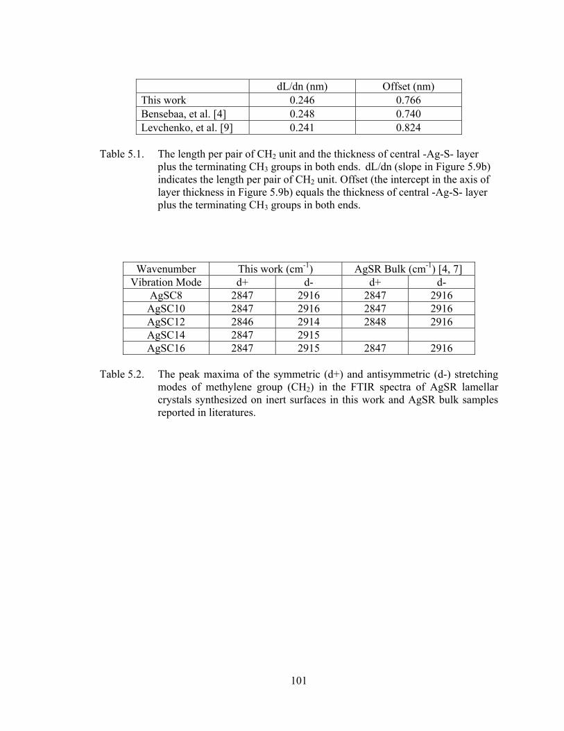
101
dL/dn (nm) Offset (nm) This work 0.246 0.766 Bensebaa, et al. [4] 0.248 0.740 Levchenko, et al. [9] 0.241 0.824
Table 5.1. The length per pair of CH2 unit and the thickness of central -Ag-S- layer
plus the terminating CH3 groups in both ends. dL/dn (slope in Figure 5.9b) indicates the length per pair of CH2 unit. Offset (the intercept in the axis of layer thickness in Figure 5.9b) equals the thickness of central -Ag-S- layer plus the terminating CH3 groups in both ends.
Wavenumber This work (cm-1) AgSR Bulk (cm-1) [4, 7] Vibration Mode d+ d- d+ d-
AgSC8 2847 2916 2847 2916 AgSC10 2847 2916 2847 2916 AgSC12 2846 2914 2848 2916 AgSC14 2847 2915 AgSC16 2847 2915 2847 2916
Table 5.2. The peak maxima of the symmetric (d+) and antisymmetric (d-) stretching
modes of methylene group (CH2) in the FTIR spectra of AgSR lamellar crystals synthesized on inert surfaces in this work and AgSR bulk samples reported in literatures.

102
CHAPTER 6
SIZE OF SILVER-ALKANETHIOLATE LAMELLAR CRYSTALS
6.1. Introduction
Extremely small polymeric silver-alkanethiolate (AgSR) lamellar crystals are
synthesized on inert surfaces through the reaction between alkanethiol and Ag clusters.
Compared to traditional polymer materials, AgSR lamellae can have very small thickness
while still keeping crystalline structure. For example, the layer spacing of AgSC10
crystals is 2.99 ± 0.01 nm. Therefore, AgSC10 crystals with only one layer have the
thickness of only 2.99 nm which is 3 times thinner than the thinnest polyethylene single-
crystal lamellae reported so far (9 nm thick).[1, 2] The thickness of the AgSR lamellae is
determined by the number of layers in the crystals, which can be controlled by adjusting
the experimental conditions during the synthesis. In this work, AgSR lamellar crystals
with only one or a few layers are successfully synthesized on inert surfaces and are
orientated with respect to the substrate. The obtained crystals have narrow dispersity, or
even mono-dispersity.
Since the properties of materials (including polymers) change as the size
decreases to nanometer scale, AgSR provides a good platform for studying size-
dependent properties in polymeric systems. Furthermore, the multilayer structure of
AgSR also makes it a perfect material for studying magic-number-size properties such as
discrete melting.
In order to study the size-dependent properties of AgSR lamellar crystals, it is
critical to control the crystal size during synthesis and to accurately measure the size of
the synthesized crystals.

103
6.2. Size Measurement
X-ray diffraction (XRD) and Atomic force microscopy (AFM) are the main
techniques used in measuring the size of AgSR lamellar crystals synthesized on inert
surfaces. The data obtained with these two techniques are complimentary to each other.
X-ray reflectivity (XRR) is also used but only limited to measure the thickness of mono-
dispersed 1-layer AgSR lamellae.
6.2.1. X-ray diffraction
XRD is used to determine the multilayer structure of AgSR phase and to calculate
the layer spacing. The obtained diffraction is also analyzed to estimate the average size
(thickness) of the multilayer AgSR crystals on the surface by using Scherrer analysis.[3]
This method is especially suitable for highly poly-dispersed samples in which AgSR
crystals with many different sizes coexist on the surface, since Scherrer analysis can give
a quick estimate on the average crystal size. It is also suitable for the samples in which
the surface lacks enough contrast for AFM measurement. For example, in an as-grown
sample (obtained after the reaction between alkanethiol and Ag clusters, but not
annealed), AgSR and MPCs phases form a composite layer on the surface, and the AgSR
phase lacks texture with respect to the substrate. It is difficult to use AFM to measure the
size of AgSR crystals in such a sample. Therefore the average crystal size is estimated via
XRD analysis.
6.2.2. X-ray reflectivity
The equipment (Philips X’pert diffractometer) used for XRD study can also be
used for XRR measurement by probing diffraction intensities at glancing angles of
incidence. The beam source is parallel Cu Kα (1.5418 Å) radiation with line focus. The
104
beam intensity is 45 kV and 40 mA. A Ni foil filter is used in front of the beam source to
attenuate Cu Kβ radiation. Compared to XRD, the signal at low-angle range (i.e 2θ < 1°
but higher than critical angle) is also included. XRR can be used to accurately measure
the thickness of thin films, but is restricted to samples with uniform thickness and
densities.[4] Therefore, in this work, it is only suitable for the AgSR lamellae samples
with mono-dispersed thickness.
6.2.3. Atomic force microscopy
6.2.3.1.Direct measurement of crystal size
AFM can directly measure the size of AgSR crystals that are synthesized on inert
surfaces. The step height in the edges of the crystals is obtained by analyzing individual
AFM line scans that cross from the substrate to the top surface of the crystals. If the
central plane of the crystals is parallel with the substrate surface, then the thickness of the
lamellae can be directly measured. Combined with the layer thickness obtained via XRD,
the exact number of layers in each crystal can be calculated.
However, the measurement is based on the assumption that the substrate areas
(the open areas between AgSR crystals in the micrographs) are clear of any materials.
This assumption is not always true in the real situation. Therefore, data correction is
necessary and will be discussed in a later section.
6.2.3.2.Size distribution
AFM study can also provide the size distribution of the crystals on the surface as
well as the average size. A histogram of the number of pixels at a particular height
obtained with AFM is plotted for each sample. For example, for the AFM micrographs
shown in Figure 6.1(a)-(e), the corresponding histograms are plotted in Figure 6.1(a')-(e')

105
sequentially. Multiple peaks are observed on the histograms. The first peak corresponds
to the substrate, and the following peak(s) correspond to the AgSR crystals with a certain
number of layers. In the ideal situation, the full-width-at-half-maxium (FWHM) should
be equal to the roughness of the surfaces of the substrate and AgSR crystals, respectively.
However, the obtained peaks have larger FWHM because of the artifacts introduced in
the measurement and data processing. For example, the FWHM of the substrate peak in
all the histograms is 1.0 – 1.2 nm and is about 2 times that of a bare Si substrate (0.5 nm)
which has not be exposed to Ag or alkanethiol.
After the peaks are identified in AFM height histograms, the peak positions are
used to determine the thickness of the lamellae. Since AgSC10 lamellar crystals are
parallel to the substrate surface, the height of the lamellae measured with AFM is
equivalent to the thickness of the crystals. Based on the layer thickness (2.99 nm for
AgSC10) determined via XRD on multilayer crystals, the AgSC10 lamellae with n
number of layers would have the height (thickness) of 2.99*n nm. After plotting
histograms of the AFM height data, the average thickness of the lamellae with a certain
number of layers equals the distance between the substrate peak and crystal peaks.
Compared to the direct measurement on individual lamellae, the thickness
obtained with this method is an average over the lamellae with the same number of
layers. Therefore, the height histogram provides a quick way to determine the sizes of the
crystals on the surface as well as the percentage of the crystals with a certain thickness
(number of layers). However, this method is also based on the assumption that the
substrate area is clear of any residue, i.e. the substrate peak in the histogram corresponds
to the real substrate and is centered at 0 nm. The existence of any residue on the substrate

106
would affect the accuracy of this method. A more accurate way to obtain the layer
spacing with AFM is to analyze the “differential” thickness which can be done for
samples having crystals of multiple sizes.
6.2.3.3.Data correction
Compared to XRD, AFM provides more detailed information about the crystal.
However, the accuracy is compromised by the experimental condition. Any residue on
the substrate area can cause errors on the thickness measurement of the lamellae. The
residue includes un-reacted alkanethiol or lying-down AgSR segments. Therefore, data
correction is necessary.
Figure 6.1 shows examples of correcting artifacts in AFM analysis and analyzing
crystal sizes. AgSC10 crystals are grown on surfaces with vapor synthesis. For the
sample shown in Figure 6.1(a), 0.28 nm of Ag is deposited onto the surface for reaction
and the substrate is annealed to 105 °C which generates individual crystals with 3, 4 and
5 layers. For the sample in Figure 6.1(b), 0.39 nm of Ag is used and the substrate is
annealed to 93°C then the sample generates individual crystals with 2, 3 and 4 layers. For
the sample in Figure 6.1(c), 0.22 nm of Ag is used and the substrate is annealed to 88 °C.
The majority of the generated AgSC10 crystals have 2 layers, while a small percentage is
composed of only 1 layer. For the sample in Figure 6.1(d), 0.20 nm of Ag is used and the
substrate is annealed to 81 °C then the sample generates individual crystals with 2 and 4
layers. Alternatively, for the sample in Figure 6.1(e), 0.13 nm of Ag is used and the
substrate is annealed to 88 °C. The sample generates mono-dispersed 1-layer AgSC10
crystals.

107
Histograms of height data can be plotted to determine the thicknesses of the
lamellae as described in the previous sections. However, if no data correction is made on
the histograms, the obtained average thicknesses would be slightly lower than the
predicted values as shown in Figure 6.1(f). The deviation increase as the annealing
temperature decreases. The deviations from theoretical values for the samples shown in
Figure 6.1(a)-(e) are summarized in Figure 6.1(g) and are plotted as a function of
annealing temperature. There is also variation among samples. These artifacts occur
because substrate area between the AgSR crystals may not be bare substrate as expected
but is fully or partially covered with thin layer of “residue” materials such as un-reacted
alkanethiol or lying-down AgSR segments which affect the thickness measurement of the
lamellae. Annealing samples to higher temperature can reduce this effect both by
evaporating the excess decanethiol and by gathering the remaining AgSC10 segments
into the large crystals.
In order to correct this artifact, the histograms are shifted rightward as shown in
Figure 6.1(a')-(e'). Therefore, the substrate peaks are not centered at 0 nm as in an ideal
situation, since they actually correspond to the residues and the real substrate is buried
underneath. After shifting the histograms, the 0 nm of the Height-axis refers to the real
substrate. The maxima of the peaks corresponding to AgSC10 lamellae now agree well to
the theoretical thickness values.
6.2.3.4.Amount of AgSR
In addition to the size measurement, AFM analysis is also used to estimate the
amount of AgSR on the surface, especially for the samples with small crystals. Since
AFM scanning obtains the topography of AgSR crystals on the surface, both the
108
thickness and the lateral dimension of the crystals are determined. The volume of the
crystals is thus determined. The density of AgSR lamellae can be calculated based on the
molecular model in which the alkyl chains are close-packed.[5] Therefore, the moles of
AgSR on a certain area of surface can be calculated.
6.3. Size control
The size of the synthesized AgSR lamellar crystals on inert surfaces is adjustable.
Since the thickness (nanometer scale) of the lamellae is much smaller than the lateral
dimension (micron scale), it has a more critical effect on the size-dependent properties,
especially for the crystals that have only a few layers. Therefore, this work is more
focused on the control of the thickness (number of layers) of the synthesized AgSR
lamellar crystals. Among the factors that can affect the crystal size, the most easily
adjusted and most controllable parameters are the amount of deposited Ag and the
annealing temperature.
6.3.1. Amount of Ag
The amount of deposited Ag on the surface determines the maximum amount of
AgSC10 that can be obtained. Assuming all the Ag clusters are involved in the reaction
with alkanethiol and are completely converted to AgSR phase, then more Ag on the
surface leads to more AgSR. However, this assumption is not always true, since the
reaction products between alkanethiol and Ag clusters depend on the cluster size. Small
cluster are less stable at the presence of excess alkanethiol and are easier to be converted
into AgSR phase, while large clusters have higher probability surviving the reaction and
transforming into MPCs.

109
The sizes of Ag clusters are directly related to the amount of Ag that is deposited
onto the surface. Figure 6.2 shows TEM micrographs of two as-deposited samples. For
the sample shown in Figure 6.2(a), 0.63 nm of Ag is deposited onto the surface. The area
number density of the clusters is 3.3 × 10⁴ clusters/μm2 and the average diameter is 3.3
nm (Figure 6.2(c)). For the sample shown in Figure 6.2(b), 0.14 nm of Ag is deposited
onto the surface. The area number density of the clusters is 2.3 × 10⁴ clusters/μm2 and the
average diameter is 2.2 nm (Figure 6.2(c)). Apparently, depositing more Ag onto the
surface leads to larger cluster size as well as higher number density.
Figure 6.3 further reveals the relation between the amount of deposited Ag and
the amount of obtained AgSR. Figure 6.3(a) shows the RBS spectra of Ag for a series of
samples. The amounts of Ag on the surface are determined by fitting the spectra.[6] The
amount of synthesized AgSR in the samples is determined with AFM analysis as
discussed earlier, and is plotted in Figure 6.3(b). For comparison, the values are all
transformed into equivalent thickness of Ag that is uniformly covering the surface. When
the amount of Ag is below 0.25 nm, all the Ag is consumed in the reaction with
alkanethiol and is completely converted into AgSR. As the amount of Ag increases, the
percentage of consumed Ag decreases. Continuous Ag thin film will be an extreme case
in which only 2D SAMs form on the surface instead of AgSR.
Based on Figure 6.3(b), in the thickness range of 0.05 – 0.5 nm, the amount of
synthesized AgSR on the surface increases as the amount of deposited Ag. This is also
the amount of Ag that is required to synthesize AgSR lamellar crystals with one or a few
layers which is one of the goals of this work.

110
On the other hand, if all the deposited Ag on the surface is consumed in forming
AgSR, then the amount of deposited Ag on the surface determines the minimum number
of layer of the crystals. Based on the molecular model of AgSR,[5] the complete reaction
between 0.18 nm of Ag and decanethiol vapor can generate a full-coverage single-layer
AgSC10 on the surface. Similarly, 0.18*n pmol of Ag on the surface can lead to the
formation of full-coverage n-layer AgSC10 single crystal. However, the formed AgSC10
crystals are not one uniform single crystal, and not always parallel to the substrate. The
lateral dimension and orientation of AgSC10 crystals are compromised by the real
surface condition. Subsequent thermal annealing promotes ripening of small crystals into
large ones which are orientated with the substrate. However, high annealing temperature
causes obsessive ripening to take place which creates crystals with large number of
layers.
6.3.2. Annealing temperature
Annealing is the last process step in the synthesis. In addition to removing
physically adsorbed alkanethiol, annealing also promotes the ripening of AgSR crystals
and the formation of textures with respect to the substrate. For example, for a sample that
has 0.55 nm of deposited Ag on the substrate surface and reacts with dodecanethiol
(C12H25SH) solution, XRD analysis shows the average crystal size is 3.5 ± 0.2 layers
before annealing but increases to 14.8 ± 1.0 layers after being annealed to 124 ºC.
Similarly, for a sample that has 0.63 nm of deposited Ag on the substrate surface and
reacts with decanethiol (C10H21SH) vapor, XRD analysis shows the average crystal size is
2.3 ± 0.2 layers before annealing but increases to 11.2 ± 0.4 layers after being annealed to
115 ºC. The diameter of the platelets in the annealed samples is large and ranges up to 1

111
μm. Therefore, annealing the samples increases the average volume of the AgSR crystals
by 100-fold due to mass transport driven by the ripening process.
Annealing temperature is even more important in the synthesis of small AgSR
crystals such as those with mono-dispersed sizes or with only a few layers. Although the
minimum number of layers is determined by the amount of Ag, annealing temperature
dramatically affect the crystal size. For example, the sample shown in Figure 6.1(a) has
0.28 nm of Ag and is less than that in the sample shown in Figure 6.1(b). However, the
annealing temperature in the former sample (105 ºC) is higher than the latter one (93 ºC),
and the obtained crystals have larger sizes.
6.4. Small AgSR crystals
6.4.1. Mono-dispersed 2-layer AgSC10 crystals
Nearly mono-dispersed 2-layer AgSC10 lamellar crystals are synthesized on the
surface by depositing 0.22 nm of Ag and annealing the sample to 88 ºC after the reaction
with decanethiol. Figure 6.4(a) shows an AFM micrograph of the sample and Figure
6.4(b) shows a 3-dimensional (3D) picture. The lamellar crystals have strong textures
with respect to the substrate surface. Crystalline characteristics such as sharp facets are
observed in the edges of the lamellae.
6.4.1.1.Crystal structure
The structure of the AgSC10 crystals and the layer spacing are determined via
XRD study. XRD pattern is shown in Figure 6.4(c) (blue curve) and is compared with
that of multilayer AgSC10 lamellar crystals (red curve). The diffraction peaks of the 2-
layer AgSC10 crystals appear at the same angles as the multilayer crystals except that the
first peak (010) shifts to a lower angle. The peaks are broader due to the smaller crystals

112
size (thickness). By indexing the (020) and (030) peaks, the same layer structure is
obtained on the 2-layer AgSC10 crystals as the multilayer crystals with the same layer
spacing. The shift of (010) peak is caused by the X-ray reflectivity signal which
convolutes with XRD pattern. Reflectivity signal is commonly obtained on thin film
samples with uniform film thickness and density. Since the studied sample has nearly
mono-dispersed 2-layer AgSC10 lamellar crystals, it is not surprising that reflectivity
signal appears and causes deviation of the obtained XRD pattern.
6.4.1.2.Crystal size
The thickness of the AgSC10 lamellae is uniform as indicated in Figure 6.1(c')
which shows the corresponding height histogram (after correction of the artifact caused
by residues). In addition to the peak for the substrate, two peaks are observed for the
AgSC10 crystals. The first peak is centered at 2.94 nm and corresponds to 1-layer
crystals. The peak is very weak since the 1-layer crystals only account for 5% of all the
crystals based on the volume. The second peak is centered at 6.04 nm and corresponds to
2-layer crystals which account for more than 90% of all the crystals.
The sizes (thicknesses) of the crystals are also determined via direct measurement
with AFM line scans. As discussed in the previous section, AFM line scans that cross
from the substrate to the top surface of the 2-layer crystals are randomly selected in the
micrograph, as annotated by the blue arrows in Figure 6.4(a). Figure 6.4(d) shows the
average line profile over 30 steps at the edges of AgSc10 crystals. For the same reason of
residue artifact, the baseline is shifted for correction. The obtained average step height is
5.99 ± 0.10 nm and is within experimental error equal to the predicted thickness of 2-
layer AgSC10 crystals (5.98 nm).

113
6.4.2. Mono-dispersed 1-layer AgSC10 crystals
Similar as the synthesis of 2-layer AgSC10 crystals, 1-layer AgSC10 crystals are
obtained by using even less Ag. This section discusses the characterization of a sample of
mono-dispersed AgSC10 crystals which are synthesized by depositing 0.13 nm of Ag and
annealing the sample to 88 ºC after the reaction with decanethiol. The synthesized 1-layer
crystals have high crystallinity and are orientated in parallel with the substrate.
6.4.2.1.Crystal structure
The 1-layer AgSC10 lamellar crystals are special as they do not have the layer-
by-layer ordering which has been constantly observed in the multilayer AgSR crystals.
XRD study on multilayer (e.g. 11 layers) AgSC10 lamellae shows sharp and clear
diffraction peaks. As the number of layers in the lamellar crystals decreases, the
diffraction peaks become weaker and broader, for example, the 2-layer AgSC10 crystals
discussed in the previous section. Predictably, when the lamellae are only composed of
one single layer of AgSC10, the periodicity of the lattice does not exist anymore and the
diffraction peaks vanish. As expected, XRD study on 1-layer AgSC10 crystals does not
show the typical diffraction patterns as obtained on the multilayer crystals.
Although the layer-by-layer ordering (multilayer structure) is lacking in this
sample, AFM and TEM studies indicate there is still in-plane ordering inside the 1-layer
AgSC10 crystals. Figure 6.5(a) shows an AFM micrograph of the sample. Figure 6.5(b)
shows a 3D picture. Two features are observed. The red area corresponds to the substrate
surface, while the yellow platelets correspond to the AgSC10 crystals which are
distributed over the entire surface. No steps are observed on these platelets, which is
consistent with the XRD result that there is no multilayer structure in this sample.

114
Characteristics of crystalline structure are observed in the platelets, such as clear facets in
the edges. Faceting is even more pronounced (up to 3 μm) in ultra large crystals produced
via ripening on carbon membrane as shown in TEM micrograph (Figure 6.5(c)), probably
because of the easier transport of AgSC10 on carbon. Therefore, it is deduced that the
alkyl chains inside the 1-layer AgSC10 lamellae are arranged in an ordered structure
which leads to the observed in-plane ordering.
6.4.2.2.Crystal size
The crystal size (thickness) of the AgSC10 lamellae is measured with AFM and
XRR, respectively. AFM analysis is performed in two ways as discussed in the earlier
section: (1) height histogram, and (2) step height at the edge of crystals. AFM height
histogram (Figure 6.1(e')) of the sample shows two peaks. Since the first peak
corresponds to the substrate, there is only one peak that corresponds to the AgSC10
crystals. This is in contrast to the multiple peaks observed in the cases of multilayer
crystals. Therefore, the lamellae on the substrate surface are of mono-dispersed thickness,
i.e. the number of layers is the same among all the crystals. The distance between the two
peaks is 2.62 ± 0.80 nm. Since only the thickness of 1-layer AgSC10 lamellae is within
this range, it is deduced that all of the AgSC10 crystals on the surface have only one layer
which is consistent with XRD study. Therefore, the thickness of the 1-layer crystals
should be equal to the distance between the two peaks in the histogram. However, this
value (2.62 ± 0.80 nm) is lower than the layer thickness (2.99 ± 0.01 nm) determined via
XRD on multilayer crystals, because of the residue on the substrate area.
The analysis of step height at the edge of AgSC10 crystals is similar as that in the
case of 2-layer crystals. AFM line scans that cross from the substrate to the top surface of

115
the platelets are randomly selected on the entire sample surface, as annotated by the blue
arrows in Figure 6.5(a). Figure 6.5(d) shows the average line profile over 60 steps. The
average step height is 2.76 ± 0.05 nm. The uncertainty is the standard error over the 60
scans. As expected, this value is also lower than 2.99 nm due to the residue in the
substrate area.
Since AFM study shows the AgSC10 lamellae on the surface have mono-
dispersed thickness and the lamellae are orientated with the substrate surface, XRR is
used to study the thickness of this 1-layer structure. The experimental result is shown as
blue curve in Figure 6.6(a). The molecular model suggests that each AgSR layer has a
–(Ag-S)– network in the center. Alkyl chains are bonded to S and extend into both
sides.[5, 7, 8] Therefore, a three-slab model is proposed for XRR fitting. Each AgSR
layer is divided into three slabs with regard to the density (Figure 6.6(b)), i.e. –(Ag-S)–
network in the center and alkyl chains at the top and the bottom. The fitted data (red
curve in Figure 6.6(a)) agrees well with the experimental data. The top and bottom slabs
of the alkyl chains are 1.44 nm and 1.25 nm thick, respectively, and the central –(Ag-S)–
network is 0.28 nm thick. Therefore, the total thickness of this AgSC10 single layer is
2.97 ± 0.10 nm, and is consistent with the layer thickness as determined in the AgSC10
multilayer crystals via XRD.
6.4.2.3.Lateral dimension
In addition to the example discussed above, several other samples of mono-
dispersed 1-layer AgSC10 crystals are also studied. These samples are synthesized using
the same method but with different amount of Ag on the surface (0.6 – 1.4 nm) and
different annealing temperature. Therefore, the amount of obtained AgSC10 is different

116
and the surface coverage is also different, as shown in AFM micrographs (Figure 6.7(a)-
(c)).
The crystal sizes of the AgSC10 lamellar crystals in each sample are studied with
AFM. AFM height histograms (Figure 6.7(a')-(c')) of all the samples indicate that the
distance between the two peaks (corresponding to the substrate and 1-layer crystals,
respectively) is smaller than the layer thickness obtained with XRD analysis (2.99 ± 0.01
nm) on multilayer (n > 10) crystals and differential thickness measurement (3.1 ± 0.1 nm)
obtained with AFM on small multilayer crystals, and is also smaller than the XRR
analysis (2.97 ± 0.10 nm) of 1-layer AgSC10. This deviation is due to the alkanethiolates
and/or alkanethiol residue on the substrate.
In addition, the distance between two peaks also varies from 2.50 to 2.90 nm in
different samples due to the variation of the thickness of the residue on the substrate. This
tendency is consistent with the annealing temperature. The lower is the annealing
temperature, the larger is the deviation.
6.5. Conclusion
In summary, XRD, XRR and AFM are employed to measure the size (thickness)
of AgSR lamellar crystals grown on inert surfaces. The information obtained with
different characterization techniques is complimentary to each other. XRD is used to
accurately determine the layer spacing, and is an easy and quick method to measure the
average size of poly-dispersed multilayer AgSR crystals. AFM analysis provides details
of individual crystals, and can be used to determine the size distribution and amount of
samples. However, data correction is required for accurate measurement.
117
The size of lamellar crystals is controlled by adjusting two parameters in the
synthesis process: the amount of deposited Ag and the annealing temperature. Small
AgSR crystals such as mono-dispersed 1-layer and nearly mono-dispersed 2-layer AgSR
lamellar crystals are successfully synthesized.
6.6. References
1. Weber, C. H. M., Chiche, A., Krausch, G., Rosenfeldt, S., Ballauff, M., Harnau, L., Gottker-Schnetmann, I., Tong, Q., Mecking, S., Single lamella nanoparticles of polyethylene. Nano Letters, 7, 2024-2029 (2007).
2. Cheng, S. Z. D., Materials science - Polymer crystals downsized. Nature, 448,
1006-1007 (2007). 3. Cullity, B. D., Stock, S. R., Elements of X-ray Diffraction. 3rd ed., Prentice Hall:
Upper Saddle River, New Jersey, 2001. 4. Als-Nielsen, J., McMorrow, D., Elements of Modern X-Ray Physics. John Wiley
& SOns: Chichester, 2001. 5. Bensebaa, F., Ellis, T. H., Kruus, E., Voicu, R., Zhou, Y., Characterization of
self-assembled bilayers: Silver-alkanethiolates. Langmuir, 14, 6579-6587 (1998). 6. Mayer, M. Proceedings of the15th International Conference on the Application of
Accelerators in Research and Industry, Denton, Texas, 1999. 7. Dance, I. G., Fisher, K. J., Banda, R. M. H., Scudder, M. L., Layered Structure of
Crystalline AgSR. Inorganic Chemistry, 30, 183-187 (1991). 8. Baena, M. J., Espinet, P., Lequerica, M. C., Levelut, A. M., Mesogenic Behavior
of Silver Thiolates with Layered Structure in the Solid-State - Covalent Soaps. Journal of the American Chemical Society, 114, 4182-4185 (1992).

118
6.7. Figures
60 80 100 120-3
-2
-1
0
1
ΔH
(nm
)
T (°C)
0
10k
20k0.06 nm
0.39 nm, 93 °C
Cou
nts
Substrate
2-layer
3-layer
4-layer
0
20k
40kSubstrate
3-layer4-layer
5-layer
0.28 nm, 105 °C0.07 nm
0
10k
20k0.22 nm, 88 °C
Substrate
1-layer
2-layer0.36 nm
-3 0 3 6 9 12 150
5k
10k
15k0.13 nm, 88 °C
Height (nm)
Substrate
1-layer0.37 nm
0 1 2 3 4 50369
1215
Hei
ght (
nm)
Layer #
(a)
(b)
(c)
(e)
(a')
(b')
(c')
(e')
(f)
(g)
0
10k
20k0.20 nm, 81 °CSubstrate
0.55 nm
1-layer2-layer
(d')
(d)
Figure 6.1. (a)-(e) AFM micrographs (5 µm × 5 µm) of AgSC10 lamellar crystals with different thicknesses. All the samples are prepared on the surface of Si wafers. (a')-(e') Histograms corresponding to the height data in (a)-(e). The data are shifted to correct the artifacts caused by the residues on substrate areas. (f) Comparing the thickness of the AgSC10 crystals measured via AFM without data correction (black squares) with those predicted based on XRD data (red curve). (g) The deviation of the thickness obtained with AFM (without data correction) as a function of annealing temperature.

119
0 1 2 3 4 5 6 70
1000
2000
3000
Clu
ster
#D
ensi
ty (1
/μm
2 )
Diameter (nm)
20 nm 20 nm
(a) (b)
(d)(c)
0 1 2 3 4 5 60
1000
2000
3000
Clu
ster
#D
ensi
ty (1
/μm
2 )
Diameter (nm)
Figure 6.2. (a) and (b) TEM micrographs of Ag clusters that form on carbon membranes via vapor deposition. Totally 0.63 nm of Ag is deposited in (a) and 0.14 nm in (b). (c) and (d) Histograms showing the size distribution of Ag clusters in (a) and (b), respectively.

120
580 590 600 870 880 890 9000
200
400
600
800
1000
1200 0.06 nm 0.13 nm 0.14 nm 0.22 nm 0.28 nm 0.39 nm
g_ p _ _
Cou
nts
Channel
(b)
(a)
0.0 0.1 0.2 0.3 0.4 0.50.0
0.1
0.2
0.3
0.4
0.5
RBS (pmol)
AFM
(nm
)
RBS (nm)
0 20 40 60 80 100 120
0
20
40
60
80
100
120
AFM
(pm
ol)
Figure 6.3. (a) RBS spectra of Ag in a series of samples prepared on the surface of Si wafers. (b) The amount of AgSC10 on the substrate surface (measured with AFM) is plotted versus the amount of Ag (measured with RBS). The data are transformed into equivalent thickness of Ag which is assumed to be uniformly distributed on the surface.

121
2 4 6 8 10101
102
103
104
105
2-Layer Multilayer
2θ (degree)
Inte
nsity
(Cou
nts/
s) (010)
(020)(030)
(b)(a)
(d)
0 100 200 300 400 500
01234567
nm
Hei
ght (
nm)
2-Layer
(c)
Figure 6.4. (a) AFM 2D (5 µm × 5 µm) and (b) 3D (2 µm × 2 µm) micrographs of nearly mono-dispersed 2-layer AgSC10 lamellar crystals grown on the surface of Si wafers. (c) XRD patterns of 2-layer (blue curve) and multilayer (11 layers on average, red curve) AgSC10 lamellar crystals. (d) An average of 30 line scans over the steps from Si substrate to AgSC10 crystals, as annotated (blue arrows) in (a).

122
0 50 100 150 2000.00.51.01.52.02.53.03.5
Hei
ght (
nm)
nm
1-layer
(a)
0.5 μm
(c)
(b)
(d)
Figure 6.5. (a) AFM 2D (2 µm × 2 µm) and (b) 3D (2 µm × 2 µm) micrographs of
mono-dispersed 1-layer AgSC10 lamellar crystals grown on the surface of Si wafers. (c) TEM micrographs of 1-layer AgSC10 crystals grown on carbon membranes; (d) An average of 60 line scans over the steps from Si substrate to AgSC10 crystals, as annotated (blue arrows) in (a).
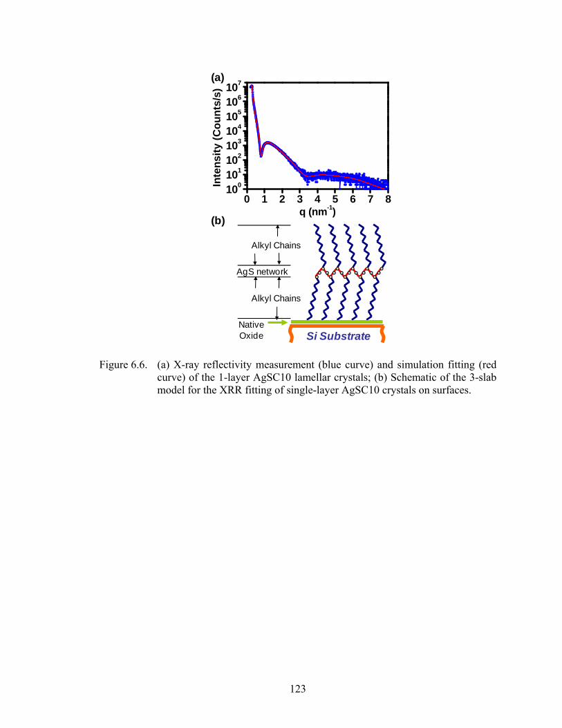
123
0 1 2 3 4 5 6 7 8100101102103104105106107
Inte
nsity
(Cou
nts/
s)q (nm-1)
(b)
Alkyl Chains
Alkyl Chains
AgS network
Si SubstrateNativeOxide
(a)
Figure 6.6. (a) X-ray reflectivity measurement (blue curve) and simulation fitting (red curve) of the 1-layer AgSC10 lamellar crystals; (b) Schematic of the 3-slab model for the XRR fitting of single-layer AgSC10 crystals on surfaces.

124
3 nm
0
-3
(a)
(b)
(c)0
5k
10k
15k 0.13 nm, 88 °C
Cou
nts
Substrate0.37 nm 1-layer
0
10k
20k0.06 nm, 59 °C
Substrate
1-layer
0.78 nm
0 30
10k
20k 0.14 nm, 81 °C
Height (nm)
Substrate0.56 nm
1-layer
(a')
(b')
(c')
Figure 6.7. (a)-(c) AFM micrographs (2 µm × 2 µm) of mono-dispersed 1-layer
AgSC10 lamellar crystals with different lateral dimensions. All the samples are prepared on the surface of Si wafers. (a')-(c') Histograms corresponding to the height data in (a)-(c). The data are shifted to correct the artifacts caused by the residues on substrate areas.

125
CHAPTER 7
SIZE-DEPENDENT MELTING OF SILVER-ALKANETHIOLATE LAMELLAR CRYSTALS
7.1. Melting characteristics of multilayer AgSR lamellar crystals
7.1.1. Melting characteristics of AgSC16
The melting transition of AgSR lamellar crystals synthesized on surfaces is
characterized with nanocalorimetry. Figure 7.1(a) shows an example of calorimetric
studies on AgSC16 crystals synthesized on surfaces. Two samples are prepared by
depositing 0.26 nm of Ag onto the substrate surface and making them react with
hexadecanethiol (C16H33SH). One sample is annealed at 120 ºC after the reaction, while
the other is not. Calorimetric measurement is performed on both the as-grown (blue curve)
and annealed (red curve) samples.
The melting transition occurs at 128 ± 3 ºC (full-width-at-half-maximum [FWHM]
~ 6.5 ºC) for the as-grown sample and 137 ± 3 ºC (FWHM ~ 7.0 ºC) for the annealed
sample. The calorimetric results are well reproducible for the samples prepared with the
same method and in the same experimental conditions. The uncertainties are determined
by including the sample-to-sample variations and the resolution of nanocalorimetry
technique. It should be noted that the melting point measured with nanocalorimetry has a
small variation with the heating rate. The difference of the melting point between the as-
grown and annealed samples is due to the size-dependent melting point depression, i.e.
the thickness of the lamellae in the as-grown sample is lower than that in the annealed
sample and causes a lower melting point.
The heat of fusion during the melting transition of AgSR lamellar crystals is
calculated by integrating the area underneath the transition peak. The molar heat of fusion

126
(Hf) is then calculated by dividing the heat of fusion with the molar amount of AgSR
phase. The total amount of the self-assembled alkanethiolate in the samples is obtained
by measuring the change in the baseline of the heat capacity ΔCp(T). However, this
amount includes both the alkanethiolate in the AgSR phase and MPCs phase, although
the majority is in the former one. It is thus necessary to calculate the real amount of
alkanthiolate in the AgSR phase. It is assumed the composition values (S-to-Ag ratio)
equals 1.0 in the AgSR phase and approximately equals 0.12 in the MPCs phase. By this
means, Hf is calculated to be 55 ± 5 kJ/mol. Although the total amount of alkanethiolate
and the overall composition ratio of S/Ag vary among experiments, the molar value Hf
(kJ/mol) of AgSR is independent as shown in Figure 7.1(b).
The values of Tm and Hf of the AgSC16 lamellar crystals synthesized on surfaces
are comparable to the values obtained by Baena et al. and Voicu, et al.[1, 2] They used
conventional DSC technique to study AgSC16 bulk samples (with an overall composition
ratio of S/Ag = 1) which are prepared through liquid-phase synthesis.[1, 2] The structure
of AgSR after the melting transition is still unclear. Baena et al. suggested that this
melting transition is a structural transition from crystal to liquid crystal (mesophases).[1]
7.1.2. Comparison with alkane, polyethylene and AgSR bulk
The melting characteristics of AgSR lamellar crystals with other chain lengths are
also studied with the same procedures as AgSC16. Similarly, the melting point is also
dependent on the size (thickness) of the lamellae. Hf is calculated with the same method
described above. The heat of fusion per repeating unit (Hf_C), the melting point (Tm), the
entropy change per repeating unit (ΔSC) are plotted versus chain length (n) and are shown
in Figure 7.2 together with those of alkane,[3] polyethylene,[3] and AgSR bulk

127
samples.[2] Hf_C of AgSR lamellar crystals synthesized on inert surfaces in this work is
comparable to that of AgSR bulk samples. In addition, Hf_C increases slightly with chain
length but is lower than that of polyethylene, probably because the arrangement of alkyl
chains is more ordered as the chain length increases.
7.2. Discrete Melting
To study the discrete melting properties, calorimetric measurements are
performed on AgSR lamellar crystals with different sizes (thicknesses). Based on Gibbs-
Thomson relation, AgSR with shorter chain length has larger difference between the
discrete melting points since (1/ )mT LΔ ∝ Δ . This helps distinguish different melting
peaks in the calorimetric curves. However, the smaller thickness of AgSR lamellae with
shorter chain length increases the relative uncertainties in the size measurement. As a
trade-off between these two concerns, AgSC10 lamellar crystals are chosen for the
systematic study of the discrete melting.
Figure 7.3(a) shows calorimetric measurement on a sample of multilayer AgSC10
lamellar crystals. A total of 0.63 nm of Ag is deposited onto substrate surfaces. After the
reaction between the formed Ag clusters and alkanethiol, the sample is annealed to 115
ºC. Scherrer analysis on XRD data estimates that the average size is about 11 layers (33
nm). The melting transition occurs at Tm = 131 ± 2 ºC (FWHM ~ 6.5 ºC) and agrees well
with AgSC10 bulk material (Tm = 132 ºC) as reported using the conventional calorimetry
technique.[1, 4] The measured heat of fusion is Hf = 30 ± 5 kJ/mol which is also the same
within experimental error as for bulk AgSC10 (32.4 kJ/mol).[1] Figure 7.3(b) shows a
corresponding AFM micrograph of the sample which demonstrates multilayer lamellar
crystals.

128
Fourier transform infrared spectroscopy (FTIR) is also used here, as the melting
transition of alkanethiolate is accompanied with the dramatic change in the
conformational order.[2, 5] The FTIR spectrum indicates a high conformational order of
the alkyl chains in the crystals (green curve in Figure 7.3(c)). The peak positions of the
symmetric (d+, 2847 cm-1) and antisymmetric (d-, 2916 cm-1) stretching modes of
methylene group (CH2) are consistent with those of AgSR bulk samples.[6] FTIR study
(Figure 7.3(c)) further reveal that the mono-dispersed 2-layer (blue curve) and mono-
dispersed 1-layer (red curve) AgSC10 crystals also have high conformational orders since
there is no shift on the peaks. However, the melting points are lower as compared to that
of multilayer crystals or bulk sample.
Figure 7.4(a) shows the schematic of a sample of nearly mono-dispersed 2-layer
AgSC10 crystals. The corresponding AFM height histogram and calorimetric result are
plotted in Figure 7.4(a') and (a"), respectively. The melting transition occurs at 122 ± 2 ºC
which is 9 ºC lower than multilayer (11-layer) crystals. Figure 7.4(b) shows the schematic
of a sample of mono-dispersed 1-layer AgSC10 crystals. The corresponding AFM height
histogram and calorimetric result are plotted in Figure 7.4(b') and (b"), respectively. The
melting transition occurs at 111 ± 2 ºC which is about 20 ºC lower than multilayer (11-
layer) crystals. Figure 7.4(c) shows the schematic of a sample composed of 1-layer and 2-
layer AgSC10 crystals. The corresponding AFM height histogram and calorimetric result
are plotted in Figure 7.4(c') and (c"), respectively. Two transition peaks are observed.
One peak is centered at 111 ± 2 ºC and corresponds to the melting of 1-layer crystals,
while the other peak is located at 118 ± 2 ºC and is close to the melting point of 2-layer
crystals.

129
Comparison of the three samples in Figure 7.4 clearly demonstrates that AgSR
lamellar crystals with different sizes (thicknesses) melt at different temperatures. The
thickness (number of layers) of the crystals has a significant effect on the melting point.
For example, the melting point of 1-layer AgSC10 is 111 ± 2 ºC and is distinguishable
from that of 2-layer AgSC10 crystals (120 ± 2 ºC). The discrete melting corresponds to
the magic-number size of the AgSC10 crystals, i.e. the number of layers (thickness).
7.3. Size-dependent melting-point depression
7.3.1. Number of layers
Calorimetric studies are also conducted on AgSC10 lamellar crystals with other
sizes (thicknesses). The crystal sizes are adjusted by using different amount of Ag and
annealing schedule. For samples that are composed of multilayer crystals with poly-
dispersed sizes, XRD study and Scherrer analysis are used to determine the average
number of layers. For the samples with small (thin) crystals or with narrow polydispersity,
AFM analysis is used to measure the size distribution and average size.
The measured melting temperatures of different samples are plotted versus the
number of layers (thickness) in Figure 7.5(a) (red squares). The melting point depression
is inversely proportional to the thickness of the lamellae and is further inversely
proportional to the number of layers (n). The demonstrated size-dependent melting-point
depression is comparable to the prediction. The equilibrium melting point ( 0mT ) of
AgSC10 lamellae with infinite thickness is calculated to be 134 ± 3 ºC by performing
linear fitting (red curve in Figure 7.5(a)) of the data and using the equation:
0 2(1 )m mf
T TH nd
σ= − (7.1)

130
in which σ = 20.5 mJ/m2,[7] and d = 2.99 nm. With the same method, the heat of fusion
(Hf) is calculated and is equivalent to 40 ± 5 kJ/mol. This value is about 25% larger than
the reported value of bulk AgSC10,[1] probably because the value of surface energy (σ)
is overestimated.
AgSR lamellar crystals with other chain lengths are also studied by using the
same method as AgSC10. For example, the melting temperatures AgSC8 lamellar
crystals are also plotted versus the number of layers in Figure 7.5(a) (blue triangles).
Similar as AgSC10, the melting point depression is inversely proportional to the number
of layers. In addition, the equilibrium melting point ( 0mT ) of AgSC8 lamellae with infinite
thickness is calculated to be 133 ± 3 ºC by performing linear fitting (red curve in Figure
7.5(a)) of the data and using Equation 7.1. The analysis procedures are the same as
AgSC10 except that d equals 2.50 nm.
7.3.2. Layer thickness
The above examples of AgSC10 and AgSC8 demonstrate that the melting point
depression is inversely proportional to the number of layers in the lamellae. However,
comparison of the melting temperatures of AgSC10 and AgSC8 lamellar crystals with
same number of layers reveals that the melting point depression is also dependent on the
layer thickness. For example, the melting point of 1-layer AgSC10 lamellae is 111 ± 2 ºC,
and is 10 ºC higher than that of 1-layer AgSC8 lamellae which is 101 ± 2 ºC, as shown in
Figure 7.5(a). This observation is consistent with Equation 7.1. If σ and Hf are constant,
then the melting point of AgSR lamellae is determined by both the number of layers (n)
and the layer thickness (d), i.e. the melting point depression is inversely proportional to
the total thickness of the lamellar crystals, as shown in Figure 7.5(b).

131
7.3.3. Lateral dimension
It should be noted that the lateral dimension of the lamellae do not affect the value
of Tm. For example, Figure 7.6 shows the calorimetric results of four samples. All of
them consist of mono-dispersed 1-layer AgSC10 crystals. However, the lateral
dimensions of the crystals are different. For the convenience of calculation, the lateral
dimension here is evaluated with the coverage of the 1-layer crystals on the surfaces.
Although the surface coverage varies from 25% to 75% among the samples, the melting
transition occurs at the same temperature (111 ± 2 ºC). This is because the lateral
dimension of the AgSC10 crystals studied in this work is in the micron-scale (0.1 – 10
µm) and is much larger than the thickness of the lamellae which is in the nanometer-scale
(3 – 75 nm).
7.4. Conclusion
In summary, the melting transition of AgSR lamellar crystals grown on inert
surfaces is characterized with nanocalorimetry. The melting characteristics (Tm, Hf, ΔS) of
multilayer AgSR lamellae are consistent with that of bulk AgSR. As the total thickness
(the product of the number of layers and the layer thickness) of the lamellar crystals
decreases, melting transition occurs at lower temperatures compared to bulk samples. The
melting point depression is inversely proportional to both the number of layers and the
layer thickness. Furthermore, discrete melting is observed, since AgSR lamellar crystals
have integer number of layers, i.e. magic-number size.
7.5. References
1. Baena, M. J., Espinet, P., Lequerica, M. C., Levelut, A. M., Mesogenic Behavior of Silver Thiolates with Layered Structure in the Solid-State - Covalent Soaps. Journal of the American Chemical Society, 114, 4182-4185 (1992).

132
2. Voicu, R., Badia, A., Morin, F., Lennox, R. B., Ellis, T. H., Thermal Behavior of a Self-Assembled Silver n-Dodecanethiolate Layered Material Monitored by DSC, FTIR, and 13 C NMR Spectroscopy. Chemistry of Materials, 12, 2646-2652 (2000).
3. The ATHAS (The Advanced THermal Analysis System) Data Bank.
http://athas.prz.edu.pl/. 4. Levchenko, A. A., Yee, C. K., Parikh, A. N., Navrotsky, A., Energetics of Self-
Assembly and Chain Confinement in Silver Alkanethiolates: Enthalpy-Entropy Interplay. Chemistry of Materials, 17, 5428-5438 (2005).
5. Bardeau, J. F., Parikh, A. N., Beers, J. D., Swanson, B. I., Phase behavior of a
structurally constrained organic-inorganic crystal: Temperature-dependent infrared spectroscopy of silver n-dodecanethiolate. Journal of Physical Chemistry B, 104, 627-635 (2000).
6. Parikh, A. N., Gillmor, S. D., Beers, J. D., Beardmore, K. M., Cutts, R. W.,
Swanson, B. I., Characterization of chain molecular assemblies in long-chain, layered silver thiolates: A joint infrared spectroscopy and x-ray diffraction study. Journal of Physical Chemistry B, 103, 2850-2861 (1999).
7. Brzoska, J. B., Benazouz, I., Rondelez, F., Silanization of Solid Substrates - a
Step toward Reproducibility. Langmuir, 10, 4367-4373 (1994).

133
7.6. Figures
1.0 1.5 2.0 2.5 3.00
20
40
60
801 0.8 0.6 0.4
40 80 120 1600
2
4
6
8
0
200
400
600
800
1000
Cp (k
J/K
·mol
)
T (°C)
Cp (n
J/K
)
(b)
(a)
Figure 7.1. (a) Calorimetric measurement (Cp(T) vs. T) of the as-grown (blue curve) and annealed (red curve) AgSC16 crystals grown on inert surfaces. The green curve is the baseline of blank nanocalorimetry sensors. (b) Comparison of molar heat of fusion (Hf) of AgSC16 in different experiments. Hf is about 55 ± 5 kJ/mol, independent of the overall Ag/S ratio, and is comparable to the value of powder AgSC16 sample measured by Baena et al[1] and Voicu, et al.[2] (reprinted with permission from Hu, L., Zhang, Z. S., Zhang, M., Efremov, M. Y., Olson, E. A., de la Rama, L. P., Kummamuru, R. K., Allen, L. H., Self-Assembly and Ripening of Polymeric Silver-Alkanethiolate Crystals on Inert Surfaces. Langmuir, 25, 9585-9595 (2009). Copyright 2009 American Chemical Society.)

134
(a)
(b)
(c)
0
1
2
3
4
5
Polyethylene n-alkane Bulk AgSR (Voicu, et al.) AgSR lamellae (this work)
Hf_
C (k
J/m
ol)
0
100
200
300
400
T m (K
)
-200
-100
0
100
200
Tm (°
C)
6 8 10 12 14 16 18 2002468
1012
ΔS C
(J/K
*mol
)
n
Figure 7.2. Comparison of (a) heat of fusion (Hf) per repeating unit, (b) melting point (Tm), (c) entropy of fusion (ΔS) per repeating unit of polyethylene, n-alkane, AgSR bulk and AgSR grown on inert surfaces.

135
2800 2850 2900 2950 3000
a.u.
Wavenumbers (cm-1)
d-
2915.5 d+
2847.0Multilayer
2-Layer
1-Layer
40 80 120 1600
200
400
600
800
Cp (n
J/K
)
T (oC)
131 °C
50 nm
0
-50
-25
25
(a)
(c)
(b)
Figure 7.3. (a) Calorimetric measurement and (b) an AFM micrograph of multilayer
AgSC10 lamellar crystals grown on inert surfaces. (c) FTIR spectra of multilayer (green curve), nearly mono-dispersed 2-layer (blue curve) and mono-dispersed 1-layer (red curve) AgSC10 lamellar crystals grown on inert surfaces.

136
0
10k
20k Substrate0.36 nm
2-layer
0
5k
10k
15k
Cou
nts
Substrate
0.37 nm 1-layer
-3 0 3 6 9 120
10k
20k
Height (nm)
Substrate0.55 nm
1-layer2-layer
0
50
100
150
Cp (n
J/K
)
40 60 80 100 120 140 1600
50
100
150
T (oC)
0
100
200
300
Substrate
Substrate
Substrate
(c')
(a')
(b')
(c)
(a)
(b)
(c")
(a")
(b")
Figure 7.4. Schematics of samples composed of (a) mono-dispersed 2-layer, (b) mono-dispersed 1-layer, and (c) 1-layer and 2-layer AgSR lamellar crystals. (a')-(c') AFM height histograms of the samples shown in (a)-(c). (a")-(c") Calorimetric measurement of the samples shown in (a)-(c).

137
90
100
110
120
130
1400.0 0.2 0.4 0.6 0.8 1.0
AgSC10 AgSC8
1/Layer #
T m (°
C)
123610 4
Layer #
1mT
nΔ ∝
90
100
110
120
130
1400.0 0.1 0.2 0.3 0.4 0.5
AgSC10 AgSC8
4
1/Thickness (nm-1)T m
(°C
)
Thickness (nm)5 231050
1 1m L n
Td
Δ ∝ ∝
(a)
(b)
Figure 7.5. Melting point (Tm) versus (a) number of layers (b) total thickness of
AgSC10 (red square) and AgSC8 (blue triangle) lamellar crystals grown on inert surfaces.

138
40 80 120 1600
50
100
150
200
111 °C
Cp (n
J/K
)T (oC)
1-layer AgSC10
Figure 7.6. Calorimetric curves of mono-dispersed 1-layer AgSC10 lamellar crystals
with different lateral dimensions. Although the surface coverage of the crystals varies from 25% to 75%, the melting transition occurs at 111 ± 2 ºC in all the samples.

139
CHAPTER 8
SUMMARY AND FUTURE WORK
8.1. Summary
The work presented in this dissertation mainly consists of two parts: (1) the size
effect of Ag substrates on the self-assembly process between Ag and alkanethiol; (2) the
size-dependent melting of silver-alkanethiolate (AgSR) lamellar crystals.
The reaction of alkanethiol with Ag continuous planar thin films and Ag clusters
grown on inert substrate surfaces are characterized and compared. The size of the Ag
substrate has a significant role in the reaction. Alkanethiol adsorb on continuous Ag thin
films and form self-assembled monolayers (SAMs). In contrast, the reaction between
alkanetiol and Ag clusters at comparable conditions is more aggressive and generates a
larger amount of alkanethiolate. Two different reaction products are obtained depending
on the size of the clusters. Small Ag clusters are more likely to be completely consumed
in the reaction and be converted into multilayer AgSR crystals, while larger Ag clusters
transform into monolayer-protected clusters (MPCs). The AgSR lamellar crystals are
initially small both in thickness and lateral dimension. However, during thermal
annealing, ripening occurs and generates large AgSR lamellae with lateral dimension in
micron-scale and thickness up to 30 layers. The layer thickness is determined by X-ray
diffraction (XRD) and atomic force microscopy (AFM). The results are consistent with
each other as well as with that of bulk samples. The crystals have facets and flat terraces
with extended area and smooth surfaces, and are orientated in parallel with the substrate
surface. On the other hand, the MPCs move laterally on the substrate surface during
thermal annealing and reorganize into a single-layer network.

140
The reaction between alkanethiol and Ag clusters in turn provides a new synthesis
method to grow AgSR lamellar crystals on inert surfaces. The crystal size can be
controlled by adjusting the amount of Ag on the surface and the annealing temperature,
and can be accurately measured by using XRD and AFM. Nanocalorimetry is used to
characterize the melting characteristics of AgSR lamellar crystals. Discrete melting
transitions are observed and are attributed to the fact that AgSR lamellar crystals always
have integer numbers of layers – the magic-number sizes. Similar as crystalline lamellae
of polyethylene, size-dependent melting is observed on AgSR lamellae. However, AgSR
lamellar crystals are also distinguished form polyethylene in that the melting point
depression is inversely proportional to the total thickness of the lamellae, i.e. it is not only
dependent on the thickness of one single layer, but also on the number of layers.
8.2. Future work
8.2.1. Synthesis
AgSR lamellar crystals are synthesized on inert substrate surfaces through the
reaction between Ag clusters and alkanethiol. The crystal sizes are controlled by
adjusting two parameters – the amount of Ag on the surfaces and the annealing
temperature. Several aspects of the synthesis can be further improved to better control the
obtained products. First, control the temperature at which the reaction takes place. This
provides another degree of freedom to control the crystal sizes. Second, integrate the
reaction and annealing steps into the vacuum chamber where nanocalorimetry
measurement is conducted. This integration reduces the transfer of samples between
different chambers and increases the efficiency. In addition, it prevents any possible
influence from air.

141
8.2.2. Characterization
Many characterization techniques are used in this work to study size effects on
self-assembly and melting of AgSR lamellar crystals. However, some structures and
properties of AgSR are still puzzles and require more studies.
First, the interfacial arrangement between neighboring layers in multilayer
lamellar crystals is unclear. It is found the melting point depression of AgSR lamellar
crystals is inversely proportional to the total thickness of the crystals, i.e. both the
thickness of one single layer of AgSR and the number of layers contribute to this size
effect. Therefore, the neighboring layers are not completely independent of each other. It
is speculated that there is lattice register between two neighboring layers. More
characterization work (TEM, XRD, etc.) is required to understand the interfacial
arrangement.
Second, although it is found thermal annealing leads to ripening of AgSR lamellar
crystals – both in the lateral dimension and along layer normal, little is known so far
about the ripening process. In-situ characterization (AFM, XRD, TEM, etc.) on samples
that are being annealed may provide a route to understand how AgSR lamellar crystals
evolve as temperature increases.
8.2.3. Materials
This work is mostly focused on the self-assembly between Ag and alkanethiol.
However, Ag can be replaced by other metals such as Au, Cu, Pd, etc. For example,
studies on gold-alkanethiolate (AuSR) have been reported.[1, 2] For reference, the layer
spacing of AuSR bulk samples [2] is shown in Figure 8.1 and is compared with those of
AgSR bulk sample [3, 4] and AgSR lamellar crystals grown on surfaces (this work). A

142
systematic study on the reaction between alkanethiol and different metals can provide a
better understanding on the role of sulfur-metal bonding in the self-assembly process.
On the other hand, alkanethiol can be replaced by other organosulfur compounds.
The endgroup of alkanethiol can be changed from methyl group (CH3-) to other
functional groups to adjust surface energy. Furthermore, the whole alkyl chains can be
replaced with other chemical structures. For example, commercially available chemicals
such as 11-bromo-1-undecanethiol [BrCH2(CH2)9CH2SH] and 1H,1H,2H,2H-
Perfluorodecanethiol [CF3(CF2)7CH2CH2SH] can be tested for the reaction with metal
clusters. It is expected that these new materials will provide more information in
understanding the self-assembly process and the role of surface/interface in the size-
dependent melting.
8.3. References
1. Kim, J. U., Cha, S. H., Shin, K., Jho, J. Y., Lee, J. C., Synthesis of gold nanoparticles from gold(I)-alkanethiolate complexes with supramolecular structures through electron beam irradiation in TEM. Journal of the American Chemical Society, 127, 9962-9963 (2005).
2. Cha, S. H., Kim, J. U., Kim, K. H., Lee, J. C., Preparation and photoluminescent
properties of gold(I)-alkanethiolate complexes having highly ordered supramolecular structures. Chemistry of Materials, 19, 6297-6303 (2007).
3. Bensebaa, F., Ellis, T. H., Kruus, E., Voicu, R., Zhou, Y., Characterization of
self-assembled bilayers: Silver-alkanethiolates. Langmuir, 14, 6579-6587 (1998). 4. Levchenko, A. A., Yee, C. K., Parikh, A. N., Navrotsky, A., Energetics of Self-
Assembly and Chain Confinement in Silver Alkanethiolates: Enthalpy-Entropy Interplay. Chemistry of Materials, 17, 5428-5438 (2005).
5. Voicu, R., Badia, A., Morin, F., Lennox, R. B., Ellis, T. H., Thermal Behavior of
a Self-Assembled Silver n-Dodecanethiolate Layered Material Monitored by DSC, FTIR, and 13 C NMR Spectroscopy. Chemistry of Materials, 12, 2646-2652 (2000).

143
8.4. Figures
0 2 4 6 8 10 12 14 16 180
1
2
3
4
5
6
Linear Fitting:7.40 + 2.48*m
7.66 + 2.46*m 7.76 + 2.54*m
AgSR bulk AgSR bulk (DSC available) AgSR lamellae (this work) AuSR bulk
Laye
r Thi
ckne
ss (n
m)
Number of CH2 Groups
Figure 8.1 Comparison of layer spacing of AgSR and AuSR which are measured with XRD. ♦ AgSR bulk samples reported by Bensebaa et al. and Levchenko et al.[3, 4] Calorimetry data are available for blue ones.[4, 5] ▲ AgSR lamellar crystals grown on surfaces reported in this work. ■ AuSR bulk samples reported by Cha et al.[2] The results of linear fitting for each set of data – the offset and the slope – are listed. m is the number of CH2 groups.
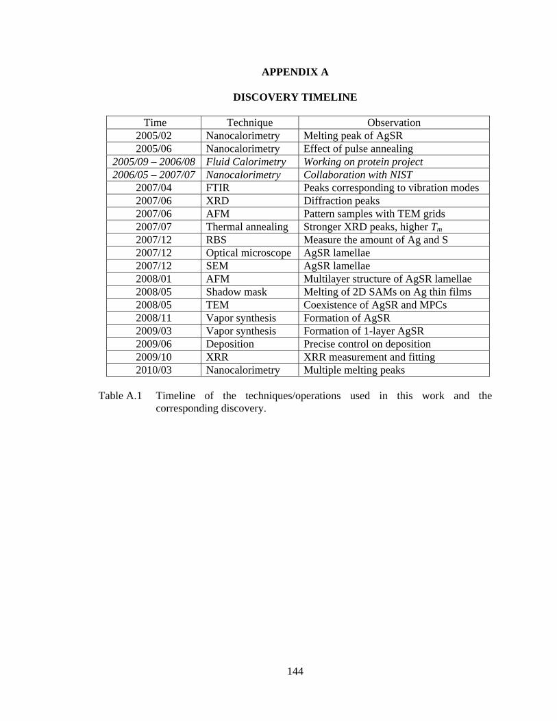
144
APPENDIX A
DISCOVERY TIMELINE
Time Technique Observation 2005/02 Nanocalorimetry Melting peak of AgSR 2005/06 Nanocalorimetry Effect of pulse annealing
2005/09 – 2006/08 Fluid Calorimetry Working on protein project 2006/05 – 2007/07 Nanocalorimetry Collaboration with NIST
2007/04 FTIR Peaks corresponding to vibration modes 2007/06 XRD Diffraction peaks 2007/06 AFM Pattern samples with TEM grids 2007/07 Thermal annealing Stronger XRD peaks, higher Tm 2007/12 RBS Measure the amount of Ag and S 2007/12 Optical microscope AgSR lamellae 2007/12 SEM AgSR lamellae 2008/01 AFM Multilayer structure of AgSR lamellae 2008/05 Shadow mask Melting of 2D SAMs on Ag thin films 2008/05 TEM Coexistence of AgSR and MPCs 2008/11 Vapor synthesis Formation of AgSR 2009/03 Vapor synthesis Formation of 1-layer AgSR 2009/06 Deposition Precise control on deposition 2009/10 XRR XRR measurement and fitting 2010/03 Nanocalorimetry Multiple melting peaks
Table A.1 Timeline of the techniques/operations used in this work and the
corresponding discovery.

145
APPENDIX B
DEPOSITION CONTROL
To synthesize AgSR lamellar crystals on inert surfaces, only a little amount of Ag
(0.05 – 0.5 nm) is deposited onto the surfaces to form Ag clusters. The amount of Ag on
the surface has a significant role in determining the amount of AgSR grown on the
surface and the crystal size. Therefore, it is necessary to have an accurate control on the
Ag deposition.
Figure B.1(a) shows the experimental setup for the thermal evaporation of Ag.
The base pressure of the deposition chamber is 5×10⁻⁸ torr and the pressure during
deposition is lower than 1×10⁻⁷ torr. The Ag source is placed in an Al2O3-coated Mo boat.
Sample holders are placed above the Ag source. A shutter is held underneath the sample
holder with the separation distance less than 1 cm. A solar cell is attached to the sample
holder and is also facing the Ag source. The solar cell is sensitive to the glowing light of
the heated source when the shutter is open, and is thus used to determine the deposition
time. A quartz crystal is set to be close to the sample holder, but is not shadowed by the
shutter. The quartz crystal is connected to a monitor outside the chamber through a
feedthrough. The tooling factor of sample-to-quartz-crystal is carefully calibrated before
experiments. Both the quartz crytal monitor (QCM) and solar cell are connected to an
analog-to-digital (ADC) card through which digital signals are acquired by a computer.
Figure B.1(b) shows the signals from QCM (voltage, blue curve) and solar cell
(current, red curve) in one deposition experiment. The time resolution is 0.2 s. Each step
in the QCM curve corresponds to 0.1 nm which is determined by the resolution of QCM.
The deposition rate is calculated via linear fitting (pink cruve) of the QCM signal. In this

146
example, the deposition rate is 0.06 nm/s. The shutter is manually opened when the
desired deposition rate is achieved and the rate is constant. The current through the solar
cell is low (~0.02 mA) when the shutter is closed, but jumps to about 0.95 mA when
being exposed to the heated Ag source, and drops back to original state (~0.02 mA) once
shutter is closed again. Both edges of the current plateau is sharp and straight inidcating
the time to open/close the shutter is less than the time resolution (0.2 s). Therefore, the
width of the plateau equals the real deposition time, and is accurate to 0.2 s. The
deposition time in this example is 9.9 ± 0.2 s. Therefore, the amout of deposited Ag is
0.59 ± 0.01 nm. The lower is the deposition rate, the more accurate is the film thickness.
In this work, the deposition rate is controled to be 0.05 – 0.5 nm/s in preparing Ag
clusters on surfaces.

147
Substrate
Ag Source
Solar cell
ADC
QuartzCrystal
Shutter
(a)
(b)
850 855 860 865 870 8752300
2320
2340
2360
2380
Time (s)
Cry
stal
Mon
itor (
mV)
0.0
0.2
0.4
0.6
0.8
1.0
Sola
r Cel
l (m
A)
Figure B.1 (a) Experimental setup to deposit Ag onto substrate surfaces. (b) An example of the deposition experiment. The blue curve shows the signal from quartz crystal monitor corresponding to the film thickness as a function of time. The red curve shows the current flowing through the solar cell.

148
APPENDIX C
STICKING COEFFICIENT OF SILVER ON SURFACES
Ag clusters are prepared on inert substrate surfaces by depositing Ag via thermal
evaporation. The substrates used in this work include: (1) double-side-polished Si wafers
with native oxide; (2) double-side-polished polished Si wafers coated with low-residual-
stress SiNx; (3) low-residual-stress SiNx membrane (in nanocalorimetry sensors); (4)
carbon membrane (on TEM copper grids). For most experiments, the amount of Ag on
the surface is in the range of 0.05 – 0.5 nm and is controlled with the method described in
Appendix B. However, the sticking coefficients of Ag on these substrates are different.
Therefore, the actual amount of Ag on different substrates may also be different. The less
is the deposited Ag, the larger is the difference.
RBS is used to measure the actual amount of Ag on the samples. Substrate (1) –
(3) can be directly used in RBS measurement, while HOPG (highly ordered pyrolytic
graphite, SPI-2 Grade) is used as substitute for substrate (4). Table C.1 shows the result
of one experiment. The samples are prepared in the same experimental condition (the
same deposition batch). Quartz crystal monitor indicates that 0.150 nm of Ag is deposited.
The actual amount of Ag on SiNx is 11% more than expected, while the amount on SiOx
and HOPG is 8% and 11% less, respectively. Similar results are also obtained in other
experiments. Therefore, it is deduced that the sticking coefficient of Ag is: SiNx > Si >
HOPG.

149
Substrate Amount (nm) Compared to QCM SiOx 0.138 -8% SiNx 0.167 +11%
HOPG 0.130 -13%
Table C.1 Comparison of the actual amount of Ag on different substrate. The target value during the deposition is 0.150 nm which is obtained via quartz crystal monitor.

150
APPENDIX D
RBS MEASUREMENT
Rutherford backscattering spectroscopy (RBS) is used to measure the actual
amount of Ag and S on the substrate surface. RBS is conducted using 2 MeV He+ with 10
– 20 nA current. The incident angle of the beam is 22.5º and the scattering angle is 150º.
However, there are two major difficulties in RBS study in this work.
First, the amount of sample is extremely small. Only 0.05 – 0.5 nm of Ag is
deposited onto the surface. The molar amount of AgSR is not more than that of Ag, since
the S/Ag ratio in AgSR is 1.0 and not all the Ag are necessarily involved in the formation
of AgSR. Although the measurement of Ag is accurate to the amount equivalent to the
thickness of 0.005 nm, the uncertainty of S is 5 – 10 times that of Ag, as S is a much
lighter element. Consequentially, the noise in the S peak in the RBS spectra raises the
difficulty in data fitting. One solution is to increase the time length of data collection. For
example, in this work the typical time used to obtain a decent S peak is 1 – 3 hours.
Second, for the measurement of samples prepared on nanocalorimetry sensors, the
small sample area (less than 1 mm2) further affects accuracy. In addition, to prevent the
Ag peak from being buried in the Pt plateau in the RBS spectra, the sensor is placed in
such a way that Pt film is on the top layer, i.e. the film stack is Pt/Ti/SiNx/AgSR. In such
an experimental condition, it is difficult to obtain an S peak that can be well fitted. Even
the Ag peak is weak and requires a long-time (> 1 hours) data collection. One solution to
this problem is to make some changes on the sensor design, for example, increasing the
width of the metal strip to increase the sample area, since sample is aligned with the
metal strip.

151
APPENDIX E
XRD ARTIFACT
X-ray diffraction is used to study the crystal structure of AgSR and to determine
the average crystal sizes. Two types of substrates are used for XRD samples: (1) double-
side-polished Si wafers with native oxide on surfaces; (2) double-side-polished Si wafers
coated with a low-residual-stress SiNx layer.
Figure E.1 shows a typical diffraction pattern of AgSC10. However, there is an
artifact (two bumps) at the 2θ angle of 11.5º – 15.5º, which is not due to the AgSC10
samples. XRD scanning is also performed on bare Si wafers either with or without SiNx
coating (Figure E.1) under the same experimental conditions. The similar bumps are also
observed at the same region. Since the Si wafers are fixed on glass slides with scotch
tapes during the measurement, XRD scanning is also conducted on bare glass slides and
tapes respectively to confirm they are not the source of the observed bumps, as shown in
Figure E.1. If it is recalled correctly, XRD staff mentioned that he also observed similar
artifact on one Si sample. It is not clear yet what is the cause of these two bumps, but it is
suspected that they are related to the azimuthal angle (φ) in placing the Si wafers on the
goniometer.
152
0 5 10 15 20
AgSC10
Inte
nsity
(a.u
.)
2θ (degree)
Si wafer
Si wafer/SiNx
Glass slide
Tape
Figure E.1 XRD patterns of AgSC10 lamellar crystals, bare Si wafers with native oxide on the surface, Si wafers coated with low-residual-stress SiNx, bare glass slide, and scotch tape.

153
APPENDIX F
BASELINE CHANGE IN NANOCALORIMETRY
Nanocalorimetry can be used to determine the amount of samples prepared on the
sensors. For a blank nanocalorimetry sensor, the baseline of the measured heat capacity is
±0.1 nJ/K since there is no sample. After samples are deposited on the sensor (aligned
with the metal strip), the baseline of the measured heat capacity would shift. To obtain
the amount of samples, the change in the baseline of the heat capacity ΔCp(T) is measured
and is then divided by the specific heat of the sample. It is assumed that the specific heat
of AgSR equals that of the alkane with the same chain length.
For an in-situ experiment, the sensors can be kept in measurement chamber (in
vacuum) without exposure to air. This can reduce the contamination or adsorption to
minimum and prevent any difference that may be caused in the operation of sensor
loading and unloading. However, in this work, after the measurement on blank sensors,
the sensors are moved out of the vacuum chamber for sample preparation and then loaded
back for further measurement. Therefore, there is a little change in the heat capacity
baseline, probably due to the adsorption of some molecules on the surface of the sensors.
Figure F.1(a) shows heat capacities measured on a blank Pt sensor at different operation
stages. The black curve corresponds to the measured heat capacity before the sensor is
moved out of the vacuum chamber, while the red curve is the 1st pulse after the sample is
moved out of and then moved back into the vacuum chamber. The change in the baseline
is 4 – 8 nJ/K in the temperature range of 40 – 120 ºC. The steeper increase in the heat
capacity starting at around 120 ºC is probably due to desorption of adsorbed molecules on
the surface which requires more heat. After being pulsed to 300 ºC, the heat capacity

154
drops back to around 0.8 nJ/K, as shown in the blue curve of Figure F.1(a). This further
supports the argument that the change in the baseline is due to adsorption of some
molecules on the sensor surface.
Another factor that influences the accuracy of heat capacity measurement is the
excess (un-reacted) alkanethiol adsorbed on the sensors. Figure F.1(b) shows the
measured heat capacity of an as-grown AgSC10 sample. The red one corresponds to the
1st pulse, while the blue corresponds to the 51th pulse. The heat capacities in the
temperature range of 140 – 160 ºC are compared and a 17% decrease is observed. It is
suggested that this difference is due to desorption of excess (un-reacted) decanethiol.
This difference can be reduced if the sample has been annealed before the measurement,
since thermal annealing can remove excess alkanethiol. Figure F.1(c) shows the
measured heat capacity of an AgSC10 sample which has been annealed to 116 ºC in
vacuum. Only a 6% difference is observed between the 1st and 51th pulses in the
temperature range of 140 – 160 ºC.

155
40 80 120 1600
200
400
600
800No Anneal
1st pulse 51th pulse
Cp (n
J/K
)
T (°C)
↓ 17%
40 80 120 1600
200
400
600
800Thermal Anneal 116 °C
1st pulse 51th pulse
Cp (n
J/K
)
T (°C)
↓ 6%
40 80 120 160
0
4
8
12 No load/unload 1st pulse after re-load 51th pulse after re-load
Cp (n
J/K
)
T (°C)
(c)
(a)
(b)
Figure F.1 (a) Heat capacities measured on a blank Pt sensor at different operation stages: before unloading the sensor from vacuum chamber (black curve); the 1st (red curve) and 51th (blue curve) pulses after the sensor is moved out of vacuum chamber and then moved back. (b) Heat capacities measured on a Pt sensor with AgSC10 sample which is not annealed in vacuum furnace. The red and blue curves correspond to the 1st and 51th pulses, respectively. (c) Heat capacities measured on a Pt sensor with AgSC10 sample which is annealed to 116 ºC in vacuum furnace. The red and blue curves correspond to the 1st and 51th pulses, respectively.

156
APPENDIX G
REVERSIBILITY IN NANOCALORIMETRY
Nanocalorimetry is extensively used in this work for thermal analysis. The fast
heating rate (5,000 – 200,000 K/s) can effectively prevent pre-annealing (ripening) of
samples before melting transitions. However, the fast scanning rate also raises
reversibility problem.
For an as-grown sample, once the sensor is pulsed to a temperature higher than
the melting point, the morphology and the crystal size of AgSR are dramatically changed.
This change is especially apparent in the 1st pulse. The sample then gradually reaches a
steady state in the following 20 – 50 pulses. Figure G.1(a) shows the measured heat
capacities of an AgSC16 sample at different states. The black curve corresponds to the 1st
pulse before which the sample is in the as-grown state as shown in Figure G.1(c). The
blue curve corresponds to the 51th pulse before which the sample is repeatedly pulsed to
180 ºC and cooled naturally in vacuum. Since the cooling rate of the sample after each
pulse is about 5,000 K/s, the sample is considered to be quenched. The corresponding
SEM micrograph is shown in Figure G.1(d) and is much different from the as-grown one.
The calorimetric curves of both as-grown and quenched samples show a sharp melting
transition peak, but the melting temperatures are different. This is probably due to the
transport of AgSC16 on the surface when it is in the melt state. Although the sample is
then quenched from the melt, the crystal size (the thickness or the number of layers in
AgSC16 lamellae) increases, which results in a higher melting point. Expectably, if the
crystal size decreases after the melting and quenching compared to the as-grown state, the

157
observed melting point would decrease. Whether the crystal sizes increase or decrease,
the change on the AgSR sample is irreversible.
In addition, the sensor can also be pulsed to temperatures lower than the melting
point of the sample to perform pulse annealing, which leads to a higher melting point
with a sharp transition peak as shown with the red curve in Figure G.1(a). However, after
being melted and quenched, the sample returns to the quenched state again. These results
are well reproducible. FTIR spectra (Figure G.1(b) of the sample in the quenched and
annealed states do not show changes on the peak positions, which indicate no changes on
the conformational order of the alkyl chains. Furthermore, no obvious morphology
change is observed in SEM (Figure G.1(e)) compared to the quenched state. More work
(e.g. AFM, XRD, TEM, etc.) will be required to find out the exact changes in the samples
during the pulse annealing. However, it is speculated that the crystal sizes of AgSR
lamellae increase – both the number of layers and the lateral dimension, and that the
registration/pairing among layers within each lamella is improved.
It should also be noted that the melting point of the annealed sample depends on
the final temperature during the pulse annealing. Figure G.2 shows the measured heat
capacities of an AgSC10 sample. Compared to the quenched state (black curve), the
sample has higher melting temperatures if they are pulse annealed (green, red and blue
curves). The higher is the final temperature in the pulse annealing, the higher is the
melting point.
Figure G.3 shows measured heat capacities of another AgSC16 sample which
experiences more complicated thermal treatments. The changes of the sample in these
processing are not fully understood yet. However, the results are shown here to provide

158
some clues for future work. The operation steps and the corresponding heat capacity
results are explained as below: (1) The black curve corresponds to the as-grown state of
the sample. There is a main peak at around 125 ºC and a broad bump at around 95 ºC.
Both of them correspond to AgSC16, but the latter one is probably due to the sporadic
small crystals of 1-layer AgSC16 on the surface. (2) After the sample is pulsed and
quenched, two peaks are observed in the heat capacity curve (blue curve). It is speculated
that the quenching process generates AgSC16 crystals with narrow poly-dispersity.
Therefore, the two peaks probably correspond to AgSC16 crystals with different numbers
of layers. (3) The sample is then annealed to 90 ºC in vacuum furnace. The measured heat
capacity is shown in red curve. Compared to the previous quenched state, the melting
peaks are stronger due to the ripening process. (4) The sample is then quenched again,
and the corresponding heat capacity is shown in the green curve. Two weak peaks are
observed. (5) The sample is then annealed again to 100 ºC in vacuum furnace. The
following heat capacity measurement (magenta curve) shows a strong peak again. The
changes in the sample during the step 4 and 5 are unclear. Many factors are involved
including the possible disturbance from air when the sample is transferred between
vacuum chambers. More experiments should be designed for better understanding.

159
2800 2850 2900 2950 3000
Quenched Annealed
d-
2914.5
a.u.
Wavenumbers (cm-1)
d+
2846.5
40 80 120 1600
500
1000
1500
2000
134 °C130.5 °C
As-grown Quenched Annealed
Cp (n
J/K
)T (°C)
136.5 °C(c)(a)
(b)
(d)
(e)
Figure G.1 (a) Heat capacities of an AgSC16 sample in as-grown (black curve), quenched (blue curve) and pulse annealed (red curve) states. (b) The corresponding FTIR spectra of the sample in the quenched and annealed states. (c) – (e) The corresponding SEM micrographs of the sample in the as-grown, quenched and annealed states.

160
100 110 120 130 1400
200
400
600
800
1000
125.5 °C
126.5 °C
129 °C
Quenched PulseAnn 116 °C PulseAnn 120 °C PulseAnn 124 °C
Cp (n
J/K
)
T (°C)
124 °C
Figure G.2 Heat capacities of an AgSC10 sample in the quenched state (black curve) and after being pulse annealed to different temperatures (green curve – 116 ºC, red curve – 120 ºC, blue curve – 124 ºC).

161
40 80 120 1600
100
200
300
400 As-grown Quenched FurAnn 90 °C Quenched FurAnn 100 °C
Cp (n
J/K
)
T (°C) Figure G.3 Heat capacities of an AgSC16 sample which is processed with the following
operations sequentially: as-grown (black curve), quenching (blue curve), annealing to 90 ºC in vacuum furnace (red curve), quenching (green curve), and annealing to 100 ºC in vacuum furnace (magenta curve).