© 2013 xiao zhang all rights reserved
TRANSCRIPT

i
v
© 2013
Xiao Zhang
ALL RIGHTS RESERVED

STRUCTURE DESIGN AND PROPERTY STUDY OF II-VI, VI-VI AND I-VII
BASED INORGANIC-ORGANIC HYBRID SEMICONDUCTORS
by
XIAO ZHANG
A Dissertation submitted to the
Graduate School – New Brunswick
Rutgers, The State University of New Jersey
in partial fulfillment of the requirements
for the degree of
Doctor of Philosophy
Graduate Program in Chemistry and Chemical Biology
written under the direction of
Professor Jing Li
and approved by
_______________________
_______________________
_______________________
_______________________
New Brunswick, New Jersey
May 2013

ii
Abstract
ABSTRACT OF THE DISSERTATION
Structure Design and Property Study of II-VI, VI-VI AND I-VII Based Inorganic-
Organic Hybrid Semiconductors
By XIAO ZHANG
Dissertation Director:
Professor Jing Li
We have developed and studied selected properties of three novel classes
of inorganic organic hybrid semiconductors based on II-VI, VI-VI and I-VII
binary phases in order to enhance the functionality over their parent structures.
As a continuing effort, we have synthesized, modified, and characterized
a number of selected structures of II-VI inorganic organic hybrid materials with
general formula ZnSe(L)0.5 (L = organic diamine). The thermal expansion
coefficients along the layer stacking (L3) axis are between -1 10-6 and 4 10-6 K-1
in the temperature range between 5K and 300K for all structures, indicating a
nearly-zero linear thermal expansion in the direction. A very small negative
iii
thermal expansion coefficient of -7.810-7 K-1 is achieved for ZnSe(ptda)0.5 along
the L3 axis, which is among the smallest values reported to date.
Secondly, we have designed a new class of inorganic organic hybrid
semiconductors under mild solvothermal conditions. By controlling the
dimensionality and topology of the VI-VI inorganic component using organic
spacers, hybrid semiconductors with tunable optical properties can be effectively
designed. The new VI-VI hybrid structures display the low thermal
conductivities and high dielectric constants caused by interface induced phonon
scattering and space charge polarization respectively. A significant negative
thermal expansion behavior was also observed in some of the new VI-VI hybrid
structures.
To further explore the unique properties of inorganic organic hybrid
semiconductors, we have developed a novel class of I-VII inorganic organic
hybrid semiconductors. A number of new 1D-CuI(L) (L = organic ligand)
inorganic organic hyrbid materials were acquired using a solvent diffusion
method. The 1D-CuI(L) hybrid structures display tunable optical absorption and
emission behavior with some structures able to give close-to–white-light
photoluminesence. By adjusting the functional group on the organic molecules,
their LUMO energy levels and the band gap of hybrid structures can be

iv
systematically tuned. This discovery further leads us to design ligand substituted
1D-CuI(L) structures to attain white light emission. We have successfully
syntheisized pyrimidine substituted CuI(pyridine) crystals which demonstrate
pure and strong white light emission, with the CIE cordinates of (0.31,0.33) under
the UV excitation.

v
AcknowledgementFirst, I would like to express my deepest gratitude to my supervisor, Prof. Jing Li,
who has provided me an opportunity to work and study in her laboratory while
providing me constant support, guidance, and encouragement throughout my graduate
career. Her enthusiasm and hard-working spirit have set an example for me, which
never fails to inspire me to overcome all the obstacles I meet both in my career and life.
I would also like to give thanks to China Scholarship Council and Rutgers
University for the financial support during my Ph.D study.
I gratefully thank Prof. Ki-Bum Lee, Prof. Tewodros Asefa, and Dr. Long Pan, not
only for serving on my thesis committee, but also for their valuable advice and
suggestions.
Many thanks to current and former group members for all the support and for
creating a joyful work environment. I would especially like to thank Mojgan Roushan
for coaching me in the synthesis and characterization of inorganic organic hybrid
semiconductors as well encouraging me to work hard on this challenging project.
Moreover, I would like to thank Dr. Debasis Banerjee for his hard work, solving the
many crystal structures. Without his help, I could not have nearly made nearly as much
progress in the project of I-VII inorganic organic hybrid semiconductor project in such a
short period of time as I have. Also I would like to thank all the undergraduate and high

vi
school students who worked with me: George, Jon and Pratyusha. I want to give my
greatest appreciation especially to George, who has worked very hard this year and
shared the pressures of a last year graduate student with me.
I would also like to thank our collaborators: Mehdi, Raj, Bill, Wenqian, Vishnu,
Yang, Tom, Ronggui and Suraj for helping me with different measurements.
I am also grateful to my parents for their love, encouragement and support.
Lastly I thank my wife, Qihan Gong, for her constant encouragement and advice
during my years of graduate work. Without her love and constant support, I would not
have the necessary diligence to complete this work.
vii
Table of ContentsAbstract ..........................................................................................................................................ii
Acknowledgement........................................................................................................................v
Table of Contents ....................................................................................................................... vii
List of Tables..................................................................................................................................x
List of Figures ..............................................................................................................................xii
1. Introduction........................................................................................................................... 1
2. II-VI inorganic organic hybrid semiconductors............................................................. 19
2.1 3D-ZnSe(L) (L = alkyl-diamine) structures ................................................................. 19
2.1.1 3D-ZnSe(en)0.5 structure ............................................................................................ 19
2.1.2 3D-ZnSe(pda)0.5 structure .......................................................................................... 24
2.1.3 3D-ZnSe(bda)0.5 structure .......................................................................................... 28
2.1.4 3D-ZnSe(ptda)0.5 structure......................................................................................... 32
2.1.5 Summary of -ZnSe(L)0.5 inorganic organic hybrid structures ........................... 35
2.2 Thermal expansion behavior of ZnSe(L) hybrid structures ..................................... 44
2.2.1 Significance of thermal expansion behavior study............................................... 44
2.2.2 Thermal expansion results and analysis. ............................................................... 47
2.3 Summary.......................................................................................................................... 61
3. VI-VI inorganic organic hybrid semiconductors ........................................................... 62
3.1 MO3(L)(L= organic ligand) structures.......................................................................... 62
3.1.1 3D-MO3(L)(L= organic ligand) structures .............................................................. 63
3.1.1.1 3D-MoO3(pyz)0.5 (pyz = pyrazine) ....................................................................... 63

viii
3.1.1.2 3D-WO3(pyz)0.5 (pyz = pyrazine) ......................................................................... 65
3.1.1.3 3D-MoO3(4,4’-bpy)0.5 (4,4’-bpy = 4,4’-bipyridine) .............................................. 66
3.1.1.4 3D-WO3(4,4’-bpy)0.5 (4,4’-bpy = 4,4’-bipyridine) ................................................ 69
3.1.1.5 3D-WO3 (bpe)0.5 (bpe = 1,2-Di-(4-bypiridyl)ethane) ............................................ 71
3.1.2 2D-MO3(L)(L= organic ligand) structures .............................................................. 73
3.1.2.1 2D-MoO3(py) (py = pyridine) .............................................................................. 73
3.1.2.1 2D-WO3(py) (py = pyridine) ................................................................................ 75
3.1.3 1D-MO3(L)(L = organic ligand) structures ............................................................. 77
3.1.3.1 1D-MoO3 (4,4’-dm-2,2’-bpy) (4,4’-dm-2,2’-bpy = 4,4’-dimethyl-2,2’-bipyridine).......................................................................................................................................... 77
3.1.3.2 1D-WO3 (4,4’-dm-2,2’-bpy) (4,4’-dm-2,2’-bpy = 4,4’-dimethyl-2,2’-bipyridine).......................................................................................................................................... 79
3.1.4 Summary of MO3(L)(L= organic ligand) structures .............................................. 81
3.2 Optical absorption properties of MO3(L) .................................................................... 85
3.3 Thermal stability of MO3(L) .......................................................................................... 92
3.4 Dielectric properties of MO3(L) .................................................................................... 96
3.5 Thermoelectric properties of MO3(L)......................................................................... 100
3.6 Thermal expansion properties of MO3(L) ................................................................. 105
3.6.1 MoO3(4,4’-bpy)0.5....................................................................................................... 105
3.6.2 WO3(4,4’-bpy)0.5......................................................................................................... 109
3.6.3 WO3(pyz)0.5 ................................................................................................................ 110
3.7 Summary........................................................................................................................ 113
4. I-VII inorganic organic hybrid semiconductors ................................................................. 115

ix
4.1 CuI(L) (L = organic ligand) structures ....................................................................... 121
4.1.1 CuI(L) (L = organic ligand) structures based on -CuI......................................... 121
4.1.1.1 3D-Cu2I2(1,3,5-triazine)..................................................................................... 121
4.1.2 CuI(L) (L = organic ligand) structures based on -CuI ......................................... 124
4.1.2.1 1D-CuI(2,6-dimethylpyrazine) .......................................................................... 124
4.1.2.2 1D-CuI(5-bromopyrimidine).............................................................................. 126
4.1.2.3 1D-CuI(3-iodopyridine) ..................................................................................... 129
4.1.2.4 1D-CuI(4-amino-5-iodopyridine)....................................................................... 131
4.1.2.5 1D-CuI(3-bromopyridine).................................................................................. 134
4.1.2.6 Pyrimidine substituted 1D-CuI(pyridine)...................................................... 137
4.2 Optical absorption and emission properties of CuI(L) (L = organic ligand)........ 140
4.2.1 3D-CuI(1,3,5-triazine)0.5............................................................................................ 140
4.2.2 1D-CuI(L) .................................................................................................................. 144
4.4 Mechanochromic properties of CuI(L) (L = organic ligand)................................... 158
4.4 Summary........................................................................................................................ 162
References .................................................................................................................................. 164

x
List of TablesTable 1: Structural information of I-VII inorganic materials. ............................................... 12
Table 2: Crystal structure data of α-ZnSe(en)0.5 (1),α- ZnSe(pda)0.5 (2),α-ZnSe(bda)0.5
(3),and α-ZnSe(ptda)0.5 (4) by Rietveld refinement. (Reproduced with permission fromref 16. Copyright © 2013 WILEY-VCH Verlag GmbH & Co. KGaA, Weinheim.)............. 37
Table 3: Atomic Coordinates and Equivalent Isotropic Temperature Factors (Å2) for 1, 2,3 and 4 at 280K. Hydrogen atoms are omitted. (Reproduced with permission from ref 16.Copyright © 2013 WILEY-VCH Verlag GmbH & Co. KGaA, Weinheim.)......................... 38
Table 4: Structural refinement information of ZnSe(en)0.5 (1) (Reproduced withpermission from ref 16. Copyright © 2013 WILEY-VCH Verlag GmbH & Co. KGaA,Weinheim.)................................................................................................................................... 40
Table 5: Structural refinement information of ZnSe(pda)0.5 (2) (Reproduced withpermission from ref 16. Copyright © 2013 WILEY-VCH Verlag GmbH & Co. KGaA,Weinheim.)................................................................................................................................... 40
Table 6: Structural refinement information of ZnSe(bda)0.5 (3) (Reproduced withpermission from ref 16. Copyright © 2013 WILEY-VCH Verlag GmbH & Co. KGaA,Weinheim.)................................................................................................................................... 41
Table 7: Structural refinement information of ZnSe(ptda)0.5 (4) (Reproduced withpermission from ref 16. Copyright © 2013 WILEY-VCH Verlag GmbH & Co. KGaA,Weinheim.)................................................................................................................................... 42
Table 8: Linear thermal expansion coefficients () of 1 - 4. (Reproduced with permissionfrom ref 16. Copyright © 2013 WILEY-VCH Verlag GmbH & Co. KGaA, Weinheim.) ... 52
Table 9: List of compounds107-109 with their unit cell parameters, space groups, and bandgaps. .............................................................................................................................................. 83
Table 10: The calculated and experimental TGA weight loss of MoO3 based inorganicorganic hybrid structures........................................................................................................... 93
Table 11: The calculated and experimental TGA weight loss of WO3 based inorganicorganic hybrid structures........................................................................................................... 95
Table 12: The experimental density and unit cell density of selected MO3(L) hybridstructures and their parent structures.................................................................................... 104

xi
Table 13: Summary of optical absorption and emission behavior of 1D-CuI(L) inorganicorganic hybrid structures......................................................................................................... 145
Table 14: Calculated HOMO and LUMO energy levels of organic molecules withdifferent basis sets..................................................................................................................... 152
Table 15: The comparison between the band gap of 1D-CuI(L) structures, calculatedLUMO energy level at B3LYP/DGDZVP and emission range. ......................................... 153
xii
List of FiguresFigure 111: View of a) single layer of honeycomb-like net of ZnS in the [MnQn(L)x]-typehybrid structure (M=Zn, Cd; Q=S, Se, Te; L = mono- or diamine), b) single-chain 1D-[MQ(L)] structure, c) double-layer 2D-[M2Q2(L)] structure, d) single-layer 2D-[MQ(L)]structure, and e) single-layer 3D-[MQ(L)0.5] structure. Blue M, red Q, in (b)–(d) the stickmodel corresponds to L. (Reproduced with permission from ref 11. Copyright © 2012WILEY-VCH Verlag GmbH & Co. KGaA, Weinheim.)........................................................... 2
Figure 211: White-light emission spectra of [Zn1.7Cd0.3S2(ha):Mn] at various Mnconcentrations (ex =365 nm). (Reproduced with permission from ref 11. Copyright ©2012 WILEY-VCH Verlag GmbH & Co. KGaA, Weinheim.).................................................. 4
Figure 3: Refined crystal structures of -[ZnSe(L)0.5] series. (a) ZnSe single-atomic slab. (b)-[ZnSe(en)0.5] (1), (c) -[ZnSe(pda)0.5] (2), (d) -[ZnSe(bda)0.5] (3), (e) -[ZnSe(ptda)0.5] (4).Hydrogen atoms are omitted for clarity. (Reproduced with permission from ref 16.Copyright © 2012 WILEY-VCH Verlag GmbH & Co. KGaA, Weinheim.)........................... 6
Figure 4: Crystal structures of (a) 3D-WO3(bpe)0.5 , (b) 2D-MoO3(py), (c) 1D-WO3 (4,4’-dimethyl-2,2’bpy), (d) MoO3 or WO3 perovskite structures. (e) Coordination environmentof 2D and 3D hybrid structure viewing from inorganic layer/organic layer stacking axis.(f) Coordination environment of 1D hybrid structure........................................................... 10
Figure 5: Structures of α-phase (left), β-phase (middle) and -phase (right) CuI and AgI.(Reproduced with permission from wikipedia website.)...................................................... 12
Figure 6: (a) Crystal structure of -CuI or -AgI (b) single-layer 3D-[Cu2I2(1,3,5-triazine)],(c) double-layer 2D-[Ag6I6(bpp)] and (d) 1D-[Cu3I3(1,3,5-triazine)] and (f) 1D-CuI(pyridine)extended network structures of I-VII hybrid materials......................................................... 16
Figure 7: Optical absorption spectrum of I-VII inorganic materials.................................... 17
Figure 8: Photoluminescence spectrum of CuI and CuBr. .................................................... 18
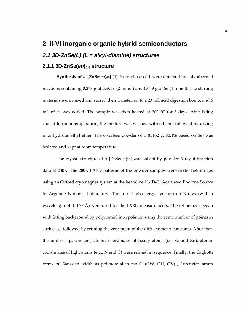
Figure 9: Observed and calculated PXRD patterns, as well as difference profile of theGSAS Rietveld refinement of the layered ZnSe(en)0.5 at 280K. Red line: simulated pattern;Black circles: experimental pattern; Green line: background of simulated pattern; Blueline: difference between the simulated and experimental data. (Reproduced withpermission from ref 16. Copyright © 2013 WILEY-VCH Verlag GmbH & Co. KGaA,Weinheim.)................................................................................................................................... 20

xiii
Figure 10: Refined crystal structures of -[ZnSe(en)0.5] (1) (a) viewing from a-axis and (b)viewing from b-axis The light blue balls are Zn; red balls, Te; blue balls, N; dark greyballs, C; Hydrogen atoms are omitted for clarity. .................................................................. 22
Figure 11: Optical absorption spectra of ZnSe(en)0.5 inorganic organic hybridsemiconductors............................................................................................................................ 23
Figure 12: Observed and calculated PXRD patterns, as well as difference profile of theGSAS Rietveld refinement of the double layered ZnSe(pda)0.5 at 280K. Black circles:experimental pattern; Red line: simulated pattern; Green line: background of simulatedpattern; Blue line: difference between the experimental and simulated data. (Reproducedwith permission from ref 16. Copyright © 2013 WILEY-VCH Verlag GmbH & Co. KGaA,Weinheim.)................................................................................................................................... 25
Figure 13: Refined crystal structures of -[ZnSe(pda)0.5] (1) (a) viewing from b-axis and (b)viewing from c-axis. The light blue balls are Zn; red balls, Te; blue balls, N; dark greyballs, C; Hydrogen atoms are omitted for clarity. .................................................................. 26
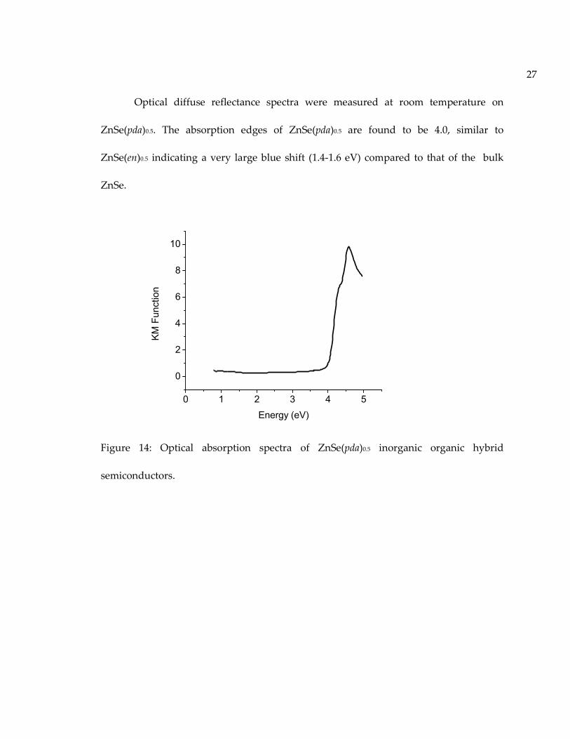
Figure 14: Optical absorption spectra of ZnSe(pda)0.5 inorganic organic hybridsemiconductors............................................................................................................................ 27
Figure 15: Observed and calculated PXRD patterns, as well as difference profile of theGSAS Rietveld refinement of the ZnSe(bda)0.5 at 280K. Black circles: experimental pattern;Red line: simulated pattern; Green line: background of simulated pattern; Blue line:difference between the experimental and simulated data. (Reproduced with permissionfrom ref 16. Copyright © 2013 WILEY-VCH Verlag GmbH & Co. KGaA, Weinheim.) ... 29
Figure 16: Refined crystal structures of -[ZnSe(bda)0.5] (3) (a) viewing from a-axis and (b)viewing from b-axis. The light blue balls are Zn; red balls, Te; blue balls, N; dark greyballs, C; Hydrogen atoms are omitted for clarity. .................................................................. 30
Figure 17: Optical absorption spectra of (a) ZnSe(bda)0.5 inorganic organic hybridsemiconductors............................................................................................................................ 31
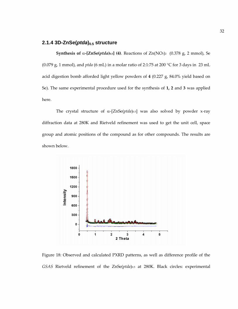
Figure 18: Observed and calculated PXRD patterns, as well as difference profile of theGSAS Rietveld refinement of the ZnSe(ptda)0.5 at 280K. Black circles: experimentalpattern; Red line: simulated pattern; Green line: background of simulated pattern; Blueline: difference between the experimental and simulated data. (Reproduced withpermission from ref 16. Copyright © 2013 WILEY-VCH Verlag GmbH & Co. KGaA,Weinheim.)................................................................................................................................... 32

xiv
Figure 19: Refined crystal structures of -[ZnSe(ptda)0.5] (1) (a) viewing from b-axis and(b) viewing from c-axis. The light blue balls are Zn; red balls, Te; blue balls, N; dark greyballs, C; Hydrogen atoms are omitted for clarity. .................................................................. 34
Figure 20: Optical absorption spectra of ZnSe(ptda)0.5 inorganic organic hybridsemiconductors............................................................................................................................ 35
Figure 21: The temperature dependent lattice constants in L1 (■) and L2 (●) forZnSe(en)0.5 (1). (Reproduced with permission from ref 16. Copyright © 2013 WILEY-VCHVerlag GmbH & Co. KGaA, Weinheim.)................................................................................. 48
Figure 22: The temperature dependent lattice constants in L1 (■) and L2 (●) forZnSe(pda)0.5 (2). (Reproduced with permission from ref 16. Copyright © 2013 WILEY-VCH Verlag GmbH & Co. KGaA, Weinheim.)....................................................................... 49
Figure 23: The temperature dependent lattice constants in L1 (■) and L2 (●) forZnSe(bda)0.5. (Reproduced with permission from ref 16. Copyright © 2013 WILEY-VCHVerlag GmbH & Co. KGaA, Weinheim.)................................................................................. 49
Figure 24: The temperature dependent lattice constants in L1 (■) and L2 (●) forZnSe(ptda)0.5 (4). (Reproduced with permission from ref 16. Copyright © 2013 WILEY-VCH Verlag GmbH & Co. KGaA, Weinheim.)....................................................................... 50
Figure 25: The temperature dependent lattice constants in L3 for (up) ZnSe(en)0.5 (1) ()and ZnSe(pda)0.5 (2) (); (down) ZnSe(bda)0.5 (3) () and ZnSe(ptda)0.5 (4)().(Reproduced with permission from ref 16. Copyright © 2013 WILEY-VCH VerlagGmbH & Co. KGaA, Weinheim.).............................................................................................. 51
Figure 26: The normallized lattice constants L1(■), L2(●)and L3(▲) for -ZnSe(en)0.5 (1)at different temperatures. (Reproduced with permission from ref 16. Copyright © 2013WILEY-VCH Verlag GmbH & Co. KGaA, Weinheim.)......................................................... 53
Figure 27: The normallized lattice constants L1(■), L2(●)and L3(▲) for -ZnSe(pda)0.5
(2), at different temperatures. (Reproduced with permission from ref 16. Copyright ©2013 WILEY-VCH Verlag GmbH & Co. KGaA, Weinheim.)................................................ 54
Figure 28: The normallized lattice constants L1(■), L2(●)and L3(▲) for-ZnSe(bda)0.5
(3) at different temperatures. (Reproduced with permission from ref 16. Copyright ©2013 WILEY-VCH Verlag GmbH & Co. KGaA, Weinheim.)................................................ 54

xv
Figure 29: The normallized lattice constants L1(■), L2(●)and L3(▲) -ZnSe(ptda)0.5 (4)at different temperatures. (Reproduced with permission from ref 16. Copyright © 2013WILEY-VCH Verlag GmbH & Co. KGaA, Weinheim.)......................................................... 55
Figure 30: Comparison of a single (110) plane of the würtzite ZnSe (left) and a singleinorganic slab of ZnSe(en)0.5 (right). The L1 and L2 axes of the ZnSe(en)0.5 structure are aand b, respectively. Zn: grey balls; Te: black balls. (Reproduced with permission from ref16. Copyright © 2013 WILEY-VCH Verlag GmbH & Co. KGaA, Weinheim.)................... 56
Figure 31: Bond distances and angles of ptda in the ZnSe(ptda)0.5 structure at 280K (top )and 5K (bottom). The closest distances between the two H atoms of the neighboring ptdaare 3.468 and 3.456Å at 280 and 5K, respectively. View is along L2 or c-axis. (Reproducedwith permission from ref 16. Copyright © 2013 WILEY-VCH Verlag GmbH & Co. KGaA,Weinheim.)................................................................................................................................... 60
Figure 32: A view of the structure of 3D-MoO3(pyz)0.5 through (a) a-axis and (b) c-axis. . 64
Figure 33: Experimental (black) and simulated (red) XRD patterns of 3D-WO3(pyz)0.5. ... 66
Figure 34: A view of the structure of 3D-MoO3(4,4’-bpy)0.5 through (a) a-axis, (b) b-axisand (c) c-axis. ............................................................................................................................... 68
Figure 35: Experimental (black) and simulated (red) XRD patterns of 3D-MoO3(4,4’-bpy)0.5. ............................................................................................................................................ 69
Figure 36: Experimental (black) and simulated (red) XRD patterns of 3D-WO3(4,4’-bpy)0.5........................................................................................................................................................ 71
Figure 37: A view of the structure of 3D-WO3 (bpe)0.5 through (a) a-axis and (b) c-axis.... 72
Figure 38: Experimental (black) and simulated (red) XRD patterns of 3D-WO3(bpe)0.5. ... 73
Figure 39: A view of the structure of 2D-MoO3(py) through (a) a-axis and (b) c-axis....... 74
Figure 40: Experimental (black) and simulated (red) XRD patterns of 2D-MoO3(py)....... 75
Figure 41: Experimental (black dots), simulated (red lines) XRD patterns of 2D-WO3(py)and differences between them (blue line)................................................................................ 77
Figure 42: A view of the structure of 1D-MoO3 (4,4’-dm-2,2’-bpy) through (left) a-axis and(right) c-axis. ................................................................................................................................ 78

xvi
Figure 43: Experimental (black) and simulated (red) XRD patterns of 1D-MoO3 (4,4’-dm-2,2’-bpy)......................................................................................................................................... 79
Figure 44: Experimental (black dots), simulated (red lines) XRD patterns of 1D-MoO3
(4,4’-dm-2,2’-bpy) and differences between them (blue line)................................................. 81
Figure 45: Crystal structures of (a) 3D-WO3(bpe)0.5 (5), (b) 2D-MoO3(py) (6), (c) 1D-WO3
(4,4’-dm-2,2’-bpy) (9), (d) MoO3 or WO3 perovskite structures. ............................................ 83
Figure 46: Optical absorption spectra of MoO3(L) inorganic organic hybridsemiconductors and the MoO3. ................................................................................................. 86
Figure 47: Band structure of 3D-MoO3(4,4’-bpy)0.5 with direct band gap of 1.685 eV........ 87
Figure 48: Band structure of 1D-MoO3 (4,4’-dm-2,2’-bpy) with direct band gap of 2.715eV........................................................................................................................................................ 88
Figure 49: Band structure of MoO3 with indirect band gap of 0.513eV............................... 88
Figure 50: Density of states of inorganic part (left) and organic part (right) of 3D-MoO3(4,4’-bpy)0.5. ......................................................................................................................... 89
Figure 51: Density of states of inorganic part (left) and organic part (right) of 1D-MoO3(4,4’-dm-2,2’-bpy) ............................................................................................................... 90
Figure 52: Optical absorption spectra of WO3(L) inorganic organic hybridsemiconductors and their parent WO3..................................................................................... 91
Figure 53: TGA profile of (a) MoO3(L) inorganic organic hybrid materials. ...................... 93
Figure 54: TGA profile of WO3(L) inorganic organic hybrid materials. .............................. 95
Figure 55: (left) Dielectric constants and (right) dielectric loss of 3D-MoO3(4,4’-bpy)0.5 atdifferent frequencies. .................................................................................................................. 97
Figure 56: (left) Dielectric constants and (right) dielectric loss of 2D-MoO3(py) at differentfrequencies. .................................................................................................................................. 98
Figure 57: (left) Dielectric constants and (right) dielectric loss of MoO3 at differentfrequencies. .................................................................................................................................. 98
Figure 58: (left) Dielectric constants and (right) dielectric loss of MoO2.5(OH)0.5(4,4’-bpy)0.5
at different frequencies............................................................................................................... 99
xvii
Figure 59: Thermal conductivities of compounds MoO3 (■), WO3 (●), MoO3(4,4’-bpy)0.5
(▲) and WO3(4,4’-bpy)0.5 (▼). .................................................................................................. 101
Figure 60: thermal diffusivities of compounds MoO3 (■), WO3 (●), MoO3(4,4’-bpy)0.5 (▲),WO3(4,4’-bpy)0.5 (▼)................................................................................................................... 102
Figure 61: Heat capacities of compounds MoO3 (black), WO3 (red), MoO3(4,4’-bpy)0.5
(blue) and WO3(4,4’-bpy)0.5 (purple)........................................................................................ 103
Figure 62: The experimental and simulated MoO3(4,4’-bpy)0.5 patterns at 28°C, and thedifferences between two patterns. .......................................................................................... 106
Figure 63: Temperature dependent lattice parameters of MoO3(4,4’-bpy)0.5 in a-axis and b-axis. ............................................................................................................................................. 106
Figure 64: Temperature dependent lattice parameters of MoO3(4,4’-bpy)0.5 in a-axis and -angle............................................................................................................................................ 107
Figure 65: Temperature dependent volume of MoO3(4,4’-bpy)0.5. ...................................... 107
Figure 66: Structural comparison between 2D-MoO3 (left) and MoO3(4,4’-bpy)0.5(right)...................................................................................................................................................... 109
Figure 67: Temperature dependent lattice parameters of a, b, c and volume of MoO3(4,4’-bpy)0.5. .......................................................................................................................................... 110
Figure 68: Temperature dependent lattice parameters of a, c and volume of WO3(pyz)0.5...................................................................................................................................................... 111
Figure 69: Temperature dependent volume of WO3(pyz)0.5................................................. 111
Figure 70: Background subtracted XRD patterns of WO3(pyz)0.5 from -30 °C to -175 °C...................................................................................................................................................... 112
Figure 71: Background subtracted XRD patterns of WO3(pyz)0.5 from -30 °C to -175 °C fortwo theta values between 22° and 29°.................................................................................... 113
Figure 72120: (left) PL spectra (λex = 350 nm) of a neat mCPy film at 77 K and CuI:mCPyfilms at rt. Inset: photo of a CuI:mCPy film under UV light (365 nm). (right) Chemicalstructure of mCPy. (Reproduced with permission from ref 120. Copyright © 2012American Chemical Society.) .................................................................................................. 118

xviii
Figure 73: The PL spectra (left) and CIE coordinates (right) of CuI(3-bromopyridine) (blackcurve and light blue circle) and CuI(5-bromopyrimidine) (red curve and light yellowcircle)........................................................................................................................................... 119
Figure 74: Left: The PL spectra of CuI(pyridine)x(pyrimidine)1-x (blue), CuI(pyridine) (red)and CuI(pyrimidine) (black). Right: CIE (coordinates) (right)of pyrimidine CuI(pyridine)...................................................................................................................................................... 120
Figure 75: Crystal structures of CuI(1,3,5-triazine)0.5 (Cu: green; I: red; N: blue; C: grey)...................................................................................................................................................... 122
Figure 76: Up: Comparison between experimental and simulated pattern of 3D-CuI(1,3,5-triazine)0.5. Down: TGA profile of CuI(1,3,5-triazine)0.5. ....................................... 123
Figure 77: Crystal structure of CuI(2,6-dimethylpyrazine). (Cu: light blue; I: purple; N:blue; C: grey).............................................................................................................................. 125
Figure 78: Top: Comparison between experimental and simulated XRD pattern ofCuI(2,6-dimethylpyrazine). Bottom: TGA profile of CuI(2,6-dimethylpyrazine). ................. 126
Figure 79: Crystal structure of CuI(5-bromopyrimidine). (Cu: light blue; I: purple; Br: green;N: blue; C: grey.) ....................................................................................................................... 127
Figure 80: Up: Comparison between experimental and simulated patterns of 3D-CuI(5-bromopyrimidine)0.5. Down: TGA profile of CuI(5-bromopyrimidine)0.5. ............................... 129
Figure 81: Crystal structures of CuI(3-iodopyridine). (Cu: light blue; I: purple; N: blue; C:grey) ............................................................................................................................................ 130
Figure 82: Up: Comparison between experimental and simulated pattern of 3D-CuI(3-iodopyridine).Down: TGA profile of CuI(3-iodopyridine). ...................................................... 131
Figure 83: Crystal structures of CuI(4-amino-5-iodopyridine)0.5. (Cu: light blue; I: purple; N:blue; C: grey).............................................................................................................................. 133
Figure 84: (a) Comparison between experimental and simulated patterns of 3D-CuI(4-amino-5-iodopyridine).(b) TGA profile of CuI(4-amino-5-iodopyridine). ............................... 134
Figure 85: Crystal structures of CuI(3-bromopyridine). (Cu: light blue; I: purple; Br: green;N: blue; C: grey) ........................................................................................................................ 135
Figure 86: (Up) Comparison between experimental and simulated XRD pattern of 3D-CuI(3-bromopyridine).(Down) TGA profile of CuI(3-bromopyridine)................................... 136

xix
Figure 87: Crystal structure of CuI(pyridine). (Cu: light blue; I: purple; N: blue; C: grey)..................................................................................................................................................... 137
Figure 88: (a) Comparison between experimental pattern of pyrimidine substitutedCuI(pyridine) and simulated pattern of CuI(pyridine).(b) TGA profile of pyrimidinesubstituted CuI(pyridine). ......................................................................................................... 139
Figure 89: Optical absorption of CuI and CuI(1,3,5-triazine)0.5. .......................................... 140
Figure 90: Band structure of CuI from DFT calculation. ..................................................... 141
Figure 91: Band structure of Cu2I2 (1,3,5-triazine) from DFT calculation........................... 142
Figure 92: Density of states of CuI from DFT calculation. .................................................. 143
Figure 93: Density of states of (a) inorganic parts and (b) organic parts of Cu2I2(1,3,5-triazine) from DFT calculation. ................................................................................................ 143
Figure 94: Photoluminesence of Cu2I2(triazine) and CuI with the excitation wavelength of320 nm......................................................................................................................................... 144
Figure 95: The optical absorption behavior of (a) CuI(4-amino-5-iodopyridine), (b) CuI(3-iodopyridine), (c) CuI(3-iodopyridine), (d) CuI(pyrdine), (e) CuI(5-bromopyrimidine), (f)CuI(pyrimidine) and (g) CuI(2,6-dimethylpyrazine). ............................................................... 147
Figure 96: Band structure of Cu2I2(4-amino-5-iodopyridine) from DFT calculation. .......... 148
Figure 97: Density of states of (a) inorganic parts and (b) organic parts of CuI(4-amino-5-iodopyridine) from DFT calculation. ........................................................................................ 148
Figure 98: Band structure of CuI(2,6-dimethylpyrizine) from DFT calculation.................. 149
Figure 99: Density of states of (a) inorganic parts and (b) organic parts of CuI(2,6-dimethylpyrizine) from DFT calculation. ................................................................................. 150
Figure 100: The PL spectra (left) and CIE coordinates (right) of CuI(3-bromopyridine)(black curve and light blue circle) and CuI(5-bromopyrimidine) (red curve and lightyellow circle). (c) Logo made from white light emitting pyrimidine substitutedCuI(pyridine) powders. ............................................................................................................. 154
Figure 101: The optical absorption spectrum of CuI(pyrimidine)0.5 (left) and CuI(pyridine)(right). ......................................................................................................................................... 156

xx
Figure 102: (a): The PL spectra of pyrimidine substituted CuI(pyridine) (blue),CuI(pyridine) (red) and CuI(pyrimidine) (black). (b): CIE coordinates of pyrimidinesubstituted CuI(pyridine). (c) Logo made from white light emitting pyrimidinesubstituted CuI(pyridine) powders. (d) Comparison between white light emittingpyrimidine substituted CuI(pyridine) crystal with other 1D-CuI(L) crystals under the UVlight. (e) Comparison between white light emitting pyrimidine substituted CuI(pyridine)crystal with other 1D-CuI(L) crystals under the ambient light. ......................................... 157
Figure 103: Photos showing the photoluminescence change of CuI(2,6-dimethylpyrazine)after (left) and before (right) griding...................................................................................... 159
Figure 104: (left) PL changes of CuI(2,6-dimethylpyrazine) before and after grinding. (right)UV changes of CuI(2,6-dimethylpyrazine) before and after grinding.................................. 159
Figure 105: Comparison of XRD patterns before (black) and after (red) griding. ........... 160
Figure 106: Photos showing the luminescence change of CuI(2,6-dimethylpyrazine) afterand before griding. ................................................................................................................... 161
Figure 107: (left) PL changes of CuI(2,6-dimethylpyrazine) before and after grinding. (right)UV changes of CuI(2,6-dimethylpyrazine) before and after grinding.................................. 161
Figure 108: Comparison of XRD patterns before (black) and after (red) griding. ........... 162

1
1. IntroductionBesides the stability and rigidity of the crystal structure, the superior properties
of solid state materials, such as electronic, optical and magnetic properties, have made
inorganic materials highly attractive in the search for new semiconducting materials.
Organic compounds built upon molecular building-blocks hold great promises for
flexibility, structural diversity, and processability. They also possess a strong potential
for the systematic control of size, shape, and symmetry. Integration and combination of
the two counterparts into a single crystal lattice may generate inorganic-organic hybrid
crystalline materials that enhance or combine the useful properties of both components.
Based on this consideration, we and others have made great effort to develop new
inorganic organic hybrid materials with different types and combinations of inorganic
and organic chemicals inside the crystal structure and to explore their unique physical
properties.1 Many examples have been reported in which organic species enter the
inorganic structures through either ionic bonding or relatively weak H-bonding and van
der Waals interactions.2-5 However, inorganic organic covalent architectures with explicit
bonding directions between electrically neutral inorganic clusters and organic molecules
are needed, but rare.6 Therefore, our research group has laid a focus on this area in the
past 10 years and has developed an unprecedented class of organic- inorganic hybrid
materials.7-10 With a general formula of [MQ(L)x](M = Mn, Zn, Cd; Q = S, Se, Te; L=

2
mono- or diamine, x = 0.5 or 1), these crystalline hybrid structures are extended one-,
two- and three- dimensional networks that are made of alternating II–VI binary
semiconductor (inorganic component) modules and organic amines (organic component)
at nano- or sub-nanometer scale and in periodic arrangement by coordinate bonds. (see
Figure 1) These new types of hybrid structures possess a number of enhanced properties
over their parent II–VI semiconductors, as well as interesting new phenomena derived
from blending of the two distinctively different components in a single crystal lattice.11
Figure 111: View of a) single layer of honeycomb-like net of ZnS in the [MnQn(L)x]-type
hybrid structure (M=Zn, Cd; Q=S, Se, Te; L = mono- or diamine), b) single-chain 1D-
[MQ(L)] structure, c) double-layer 2D-[M2Q2(L)] structure, d) single-layer 2D-[MQ(L)]
structure, and e) single-layer 3D-[MQ(L)0.5] structure. Blue M, red Q, in (b)–(d) the stick
model corresponds to L. (Reproduced with permission from ref 11. Copyright © 2012
WILEY-VCH Verlag GmbH & Co. KGaA, Weinheim.)
3
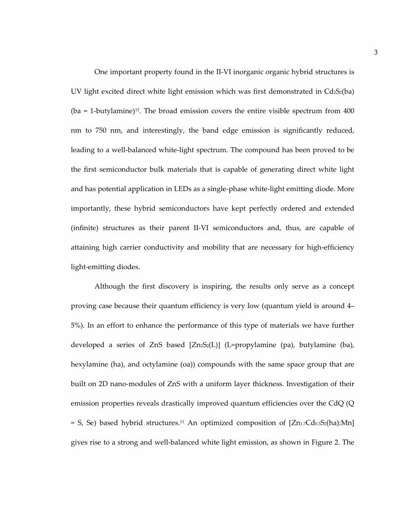
One important property found in the II-VI inorganic organic hybrid structures is
UV light excited direct white light emission which was first demonstrated in Cd2S2(ba)
(ba = 1-butylamine)12. The broad emission covers the entire visible spectrum from 400
nm to 750 nm, and interestingly, the band edge emission is significantly reduced,
leading to a well-balanced white-light spectrum. The compound has been proved to be
the first semiconductor bulk materials that is capable of generating direct white light
and has potential application in LEDs as a single-phase white-light emitting diode. More
importantly, these hybrid semiconductors have kept perfectly ordered and extended
(infinite) structures as their parent II-VI semiconductors and, thus, are capable of
attaining high carrier conductivity and mobility that are necessary for high-efficiency
light-emitting diodes.
Although the first discovery is inspiring, the results only serve as a concept
proving case because their quantum efficiency is very low (quantum yield is around 4–
5%). In an effort to enhance the performance of this type of materials we have further
developed a series of ZnS based [Zn2S2(L)] (L=propylamine (pa), butylamine (ba),
hexylamine (ha), and octylamine (oa)) compounds with the same space group that are
built on 2D nano-modules of ZnS with a uniform layer thickness. Investigation of their
emission properties reveals drastically improved quantum efficiencies over the CdQ (Q
= S, Se) based hybrid structures.11 An optimized composition of [Zn1.7Cd0.3S2(ha):Mn]
gives rise to a strong and well-balanced white light emission, as shown in Figure 2. The

4
International Commission on Illumination (CIE) coordinates of [Zn1.7Cd0.3S2(ha):Mn] are
calculated to be (0.31, 0.29), which are well within the white region of the colour space
chromaticity diagram. The quantum yield has also been strongly enhanced to 31–37%, a
value that is approaching some of the phosphors currently used in commercial WLED
productions.
Figure 211: White-light emission spectra of [Zn1.7Cd0.3S2(ha):Mn] at various Mn
concentrations (ex =365 nm). (Reproduced with permission from ref 11. Copyright ©
2012 WILEY-VCH Verlag GmbH & Co. KGaA, Weinheim.)
Another interesting phenomenon found in II-VI inorganic organic hybrid materials is
nearly zero thermal expansion (ZTE). In general crystal structures expand when the
temperature increase and contract when the temperature decrease, so there are very few
materials exhibit zero thermal expansion, that is, the length and volume of the material
are independent of temperature change. This phenomenon is even rare with the
materials which are appropriate for electronic and optoelectronic applications.13 The first

5
inorganic organic hybrid structure to demonstrate the zero thermal expansion is
ZnTe(en)0.5 (en denotes ethylenediamine) which showed uniaxial ZTE in a very broad
temperature range of 4–400 K, and concurrently possesses superior electronic and
optical properties. The ZTE behavior is caused by the compensation of contraction and
expansion of different segments along the inorganic-organic stacking axis.14 To be
specific, the inorganic component (ZnTe) remains to be positive thermal expansion (PTE)
but the organic diamine shows strong negative thermal expansion NTE in the hybrid
structure. This study suggests that hybrid structures may have the following advantages
as possible candidates for ZTE materials: (a) ZTE may be achieved by the two opposing
effect (PTE and NTE) within a single crystal lattice to avoid grain boundary associated
cracks, and (b) both PTE and NTE can be independently and systematically tuned by
varying the inorganic layers and organic molecules.15

6
Figure 3: Refined crystal structures of -[ZnSe(L)0.5] series. (a) ZnSe single-atomic slab. (b)
-[ZnSe(en)0.5] (1), (c) -[ZnSe(pda)0.5] (2), (d) -[ZnSe(bda)0.5] (3), (e) -[ZnSe(ptda)0.5] (4).
Hydrogen atoms are omitted for clarity. (Reproduced with permission from ref 16.
Copyright © 2012 WILEY-VCH Verlag GmbH & Co. KGaA, Weinheim.)
As an extension of previous work, we report a family of inorganic-organic hybrid
semiconductors with a general formula of ZnSe(L)0.5 (L = organic diamine) that exhibit
nearly-zero thermal expansion along the layer-stacking axis in the temperature range of
5-300K.16 The unit cell parameters and crystal structures of ZnSe(en)0.5, ZnSe(pda)0.5,
(
a
)
(
b
)
(
a)
(
b)
(
c)
(
d)
(
e)

7
ZnSe(bda)0.5 and ZnSe(ptda)0.5 (en = ethylenediamine, pda = propanediamine, bda =
butanediamine, and ptda = pentanediamine) are refined by Rietveld method using
powder samples, and their thermal expansion properties are analyzed and rationalized
based on their crystal structures and symmetry. ZnSe(ptda)0.5 features a very small
negative linear thermal expansion coefficient (-7.810-7 K-1) that approaches the smallest
values reported to date. Details about the results will be discussed in Chapter 1
Inspired by the success obtained from II-VI chalcogenide derived hybrid
semiconductors, we are further looking into important oxide semiconductors as parent
structures for new hybrid systems. The WO3 and MoO3 semiconductors and their
derivatives have been extensively studied owing to their unusual electric, optic and
thermal properties with many potential applications.17-32 For example, WO3 has widely
been studied in photochemical water oxidation due to its desirable band structure. WO3
is an indirect band gap semiconductor (band gap is ~2.5–2.8 eV) that can capture
approximately 12% of the solar spectrum and can absorb light in the visible spectrum up
to 500 nm. The band gap of WO3 is a more suitable for photoelectrochemical water
splitting than TiO2 (band gap is ~3.0–3.2 eV) since TiO2 absorbs only in the ultraviolet
region of the spectrum and captures approximately 4% of solar irradiation. The
theoretical maximum conversion efficiency of solar energy into H2 is merely 2.2% in a
photoelectrochemical cell using TiO2 as a photoanode and is approximately 4.8% using
WO3 as a photoanode. Furthermore, WO3 exhibits attractive photo stability and chemical

8
stability in acidic aqueous solutions (pH = 4) under solar illumination. In addition, WO3
has a moderate hole diffusion length (B150 nm) compared with -Fe2O3 (2–4 nm) and
TiO2 (104 nm) and inherently good electron transport properties. In recent years to
further increase water oxidation efficiency and photoelectric conversion efficiency,
people have made great efforts in adjusting the band gap and femi level by making
nanostructures or doping in WO3.33-35
WO3 have also been most extensively studied as electrochromic window due to
the outstanding coloration efficiency. Up until now, WO3 films have exhibited the
highest coloration efficiency in the visible region of the electromagnetic spectrum. By
fabricating EC films from crystalline WO3 nanoparticles, the state-of-the-art technology
of producing Electrochromic materials has been largely improved. Nanoparticle films
deposited by electrophoresis exhibit vastly superior electrochemical-cycling stability in
acidic electrolytes, a higher charge density, and comparable coloration efficiency.
MoO3, with same perovskite crystal structure as WO3, is a well-known lithium
insertion compound and was investigated from the early years of lithium battery
research.36-66 Sodium-substituted molybdenum oxide was shown to have a high initial
capacity of 940 mAh/g when cycled in a voltage window of 3.0–0.005V, but this material
suffered from poor cycling stability, with the capacity degrading to 400 mAh/g in 100
cycles. By increasing the cut-off potential to 0.2V and employing a slow rate (discharge
and charge at C/15 and C/20, respectively), the cycling was more stable, ranging from
9
600–400 mAh/g in 100 cycles. More recently, the anodes fabricated from crystalline
MoO3 nanoparticles perform both a durable high rate capability and durable reversible
capacity of 630 mAh/g with no capacity degradation for 150 cycles between 3.5 to 0.005V
with both charge and discharge at C/2. This result is appealing compared to micrometer-
sized particles where the capacity quickly fades.57,59
Furthermore, MoO3 could be also combined with polymers to make composite
thermoelectric source. 67 By increasing the interface induced phonon scattering, the
thermoconductivity is apparently reduced, which is the most important approach to
increase figure of merit in thermoelectrics.
10
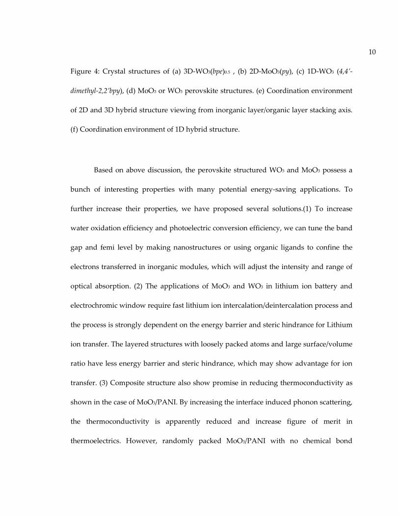
Figure 4: Crystal structures of (a) 3D-WO3(bpe)0.5 , (b) 2D-MoO3(py), (c) 1D-WO3 (4,4’-
dimethyl-2,2’bpy), (d) MoO3 or WO3 perovskite structures. (e) Coordination environment
of 2D and 3D hybrid structure viewing from inorganic layer/organic layer stacking axis.
(f) Coordination environment of 1D hybrid structure.
Based on above discussion, the perovskite structured WO3 and MoO3 possess a
bunch of interesting properties with many potential energy-saving applications. To
further increase their properties, we have proposed several solutions.(1) To increase
water oxidation efficiency and photoelectric conversion efficiency, we can tune the band
gap and femi level by making nanostructures or using organic ligands to confine the
electrons transferred in inorganic modules, which will adjust the intensity and range of
optical absorption. (2) The applications of MoO3 and WO3 in lithium ion battery and
electrochromic window require fast lithium ion intercalation/deintercalation process and
the process is strongly dependent on the energy barrier and steric hindrance for Lithium
ion transfer. The layered structures with loosely packed atoms and large surface/volume
ratio have less energy barrier and steric hindrance, which may show advantage for ion
transfer. (3) Composite structure also show promise in reducing thermoconductivity as
shown in the case of MoO3/PANI. By increasing the interface induced phonon scattering,
the thermoconductivity is apparently reduced and increase figure of merit in
thermoelectrics. However, randomly packed MoO3/PANI with no chemical bond
11
between MoO3 and polymers suffers from poor conductivity and low thermal stability
that prevent it from practical applications.67 If the MoO3 and organic molecules can be
integrated into single crystal lattice, the ordered structure with continuous inorganic
modules may increase the conductivity and thermal stability of hybrid composite while
keeping the large interface of MoO3 for phonon scattering.
Based on facts and considerations stated above, we have designed a novel system
of MO3(L) (L=organic linker) that contain 1D, 2D and 3D periodically ordered
nanostructures under mild solvothermal conditions. The results are shown in chapter 2.
By inserting different neutral organic linkers inside the parent MO3 perovskite structure,
tunable band structures, chainlike and layered inorganic VI-VI structural motifs, and
desired interfaces between inorganic and organic layers can be achieved.
Inspired by the success of II-VI and VI-VI inorganic organic hybrid systems, we
have tried further to develop new I-VII inorganic organic hybrid structures and explore
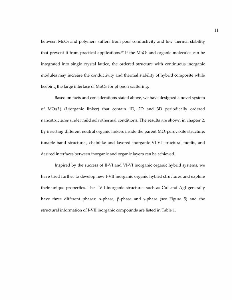
their unique properties. The I-VII inorganic structures such as CuI and AgI generally
have three different phases: α-phase, β-phase and -phase (see Figure 5) and the
structural information of I-VII inorganic compounds are listed in Table 1.

12
Figure 5: Structures of α-phase (left), β-phase (middle) and -phase (right) CuI and AgI.
(Reproduced with permission from wikipedia website.)
Table 1: Structural information of I-VII inorganic materials.
Chemicals Space group Structure
type
Unit cell parameters
α-CuI1 Fm-3m RS a = 6.16866(6) (Å)
β-CuI2 P63mc WZ a = 4.31 (Å)
c = 7.09 (Å)
-CuI1 F-43m ZB a = 6.05844(3) (Å)
α-CuBr3 Fm-3m RS a = 4.601 (Å)
β-CuBr2 P63mc WZ a = 4.06 (Å)
c = 6.66 (Å)
-CuBr5 F-43m ZB a = 5.684 (Å)

13
α-CuCl6 Fm-3m RS a = 4.9290 (Å)
-CuCl7 F-43m ZB a = 5.4202(2) (Å)
α-AgI8 Fm-3m RS a = 6.495 (Å)
β-AgI9 P63mc WZ a = 4.599(3) (Å)
c = 7.520(5) (Å)
-AgI4 F-43m ZB a = 6.493(5) (Å)
-AgBr10 F-43m ZB a = 5.7721(2) (Å)
α-AgCl10 Fm-3m ZB a = 5.5463(2) (Å)
References for the structural information of these compounds:
1. J. Mater. Chem., 2006, 16, 4393
2. Zeitschrift fuer Naturforschung, Teil A. Physikalische Chemie , 1952, 7, 369
3. Electrochimica Acta, 1977, 22, 701
4. Phase Transition, 1992, 38, 127
5. Comptes Rendus Hebdomadaires des Seances de l'Academie des Sciences, 1955,
241, 69
6. Physical Review, B - Condensed Matter, 1994, 50, 5868
7. Journal of Physics C, 1983, 16, 3673
8. Proceedings of the National Academy of Sciences, U.S.A.1962, 48, 983
9. Solid State Communications, 1977, 24, 411
10. Physical Review, B - Condensed Matter, 1999, 59, 750

14
The α-phase I-VII compounds have the rock salt structure, in which each ion is
surrounded by six ions of the opposite charge as expected on electrostatic grounds. The
surrounding ions are located at the vertices of a regular octahedron. The space group is
Fm-3m for α-phase I-VII. The β-phase I-VII compounds crystallize in wurzite structure,
which is a member of the hexagonal crystal system and consists of tetrahedrally
coordinated cations and anions that are stacked in an ABABAB pattern. The space group
of β-phase I-VII compounds is P63mc. The -phase represent zinc blende structure in I-
VII compounds which have tetrahedral coordination: each atom's nearest neighbors
consist of four atoms of the opposite type, positioned like the four vertices of a regular
tetrahedron. It is worth mentioning that the wurzite and zinc blende phases that I-VII
compounds have are also observed in II-VI materials such as ZnS, ZnSe and ZnTe, so the
basic idea of designing II-VI hybrid structures can be also applied to the design of I-VII
hybrid structures. Therefore, the I-VII inorganic organic hybrid structures can be formed
when the charge-balanced slices or chains from CuI or AgI are interconnected with
neutral organic ligands (e.g. organic diamines). 3D-Cu3I3(1,3,5-triazine)68, 2D-AgI(bpp)69,
and 1D-Cu3I3(1,3,5-triazine)68 compounds represent the 3D, 2D and 1D structures of I-VII
hybrid system correspondingly. In addition to wurzite and zinc blende structure, copper
iodide can also crystallize in the rock salt structure. It is also possible to select
electronically neutral atomic layers or chains from the rock salt CuI structure, while
keeping the atomic ratio and bonding type in the selected layers and chains same as its

15
parent structure.69-73 When connecting electronically neutral atomic layers and chains
with different organic ligands, it is also possible to produce -CuI based inorganic
organic hybrid semiconductors.
(a) (b)
(c) (d)

16
(f)
Figure 6: (a) Crystal structure of -CuI or -AgI (b) single-layer 3D-[Cu2I2(1,3,5-triazine)],
(c) double-layer 2D-[Ag6I6(bpp)] and (d) 1D-[Cu3I3(1,3,5-triazine)] and (f) 1D-CuI(pyridine)
extended network structures of I-VII hybrid materials.
As mentioned earlier in this chapter, the II-VI inorganic organic hybrid structures
generally have strong UV absorption and photoluminescence. Though greatly enhanced,
these properties can be seen as being inherited from their parent ZnS, ZnSe and ZnTe
structures. Therefore, when considering whether I-VII hybrids also have unique optical
properties similar to the II-VI hybrids, it is necessary to figure out how their parent
structures behave optically.
Figure 5 shows the optical absorption properties of I-VII materials. For the
copper halides, the CuI and CuBr display similar band gap value of 2.9 eV and CuI
shows stronger absorption edge. The absorption of CuCl is weak and is difficult to

17
distinguish the band gap. A similar trend is also observed in silver halides, in which AgI
shows much better absorption than AgBr and AgCl. AgI and AgBr have a similar band
gap of 2.75 eV. Among all the copper halides and silver halides, only CuI and CuBr
exhibit very good photoluminescence between 400nm and 450nm.
Figure 7: Optical absorption spectrum of I-VII inorganic materials

18
Figure 8: Photoluminescence spectrum of CuI and CuBr.
Based on the comparison of optical behaviors among I-VII parent materials, we
have selected CuI as the parent structure to design our inorganic organic hybrid
materials on. The strong optical absorption and emission properties of the original
parent structure make this an ideal system to modify in the pursuit of interesting optical
properties. A series of new CuI(L) inorganic organic hybrid structures were prepared
with the solution diffusion method. These structures have shown very interesting
fluorescence behavior including direct white light emission as did our II-VI hybrid
materials. Compared to our II-VI hybrid materials, the fluorescence is even stronger and
shows better thermal stability, which gives this material great promise in applications
such as light emitting diodes. The results will be summarized in chapter 4.
19
2. II-VI inorganic organic hybrid semiconductors
2.1 3D-ZnSe(L) (L = alkyl-diamine) structures
2.1.1 3D-ZnSe(en)0.5 structure
Synthesis of -[ZnSe(en)0.5] (1). Pure phase of 1 were obtained by solvothermal
reactions containing 0.273 g of ZnCl2 (2 mmol) and 0.079 g of Se (1 mmol). The starting
materials were mixed and stirred then transferred to a 23 mL acid digestion bomb, and 6
mL of en was added. The sample was then heated at 200 °C for 3 days. After being
cooled to room temperature, the mixture was washed with ethanol followed by drying
in anhydrous ethyl ether. The colorless powder of 1 (0.162 g, 90.1% based on Se) was
isolated and kept at room temperature.
The crystal structure of -[ZnSe(en)0.5] was solved by powder X-ray diffraction
data at 280K. The 280K PXRD patterns of the powder samples were under helium gas
using an Oxford cryomagnet system at the beamline 11-ID-C, Advanced Photone Source
in Argonne National Laboratory. The ultra-high-energy synchrotron X-rays (with a
wavelength of 0.1077 Å) were used for the PXRD measurements. The refinement began
with fitting background by polynomial interpolation using the same number of points in
each case, followed by refining the zero point of the diffractometer constants. After that,
the unit cell parameters, atomic coordinates of heavy atoms (i.e. Se and Zn), atomic
coordinates of light atoms (e.g., N and C) were refined in sequence. Finally, the Cagliotti
terms of Gaussian width as polynomial in tan , (GW, GU, GV) , Lorenzian strain
20
broadening (LY) and Lorenzian crystallite size (Scherrer) broadening (LX) were added
as refinable parameters in sequence and refined with high damping factor to adjust the
peak shape. The results of observed and calculated PXRD patterns, as well as difference
profile of the GSAS Rietveld refinement are shown in Figure 6.
Figure 9: Observed and calculated PXRD patterns, as well as difference profile of the
GSAS Rietveld refinement of the layered ZnSe(en)0.5 at 280K. Red line: simulated pattern;
Black circles: experimental pattern; Green line: background of simulated pattern; Blue
line: difference between the simulated and experimental data. (Reproduced with
permission from ref 16. Copyright © 2013 WILEY-VCH Verlag GmbH & Co. KGaA,
Weinheim.)

21
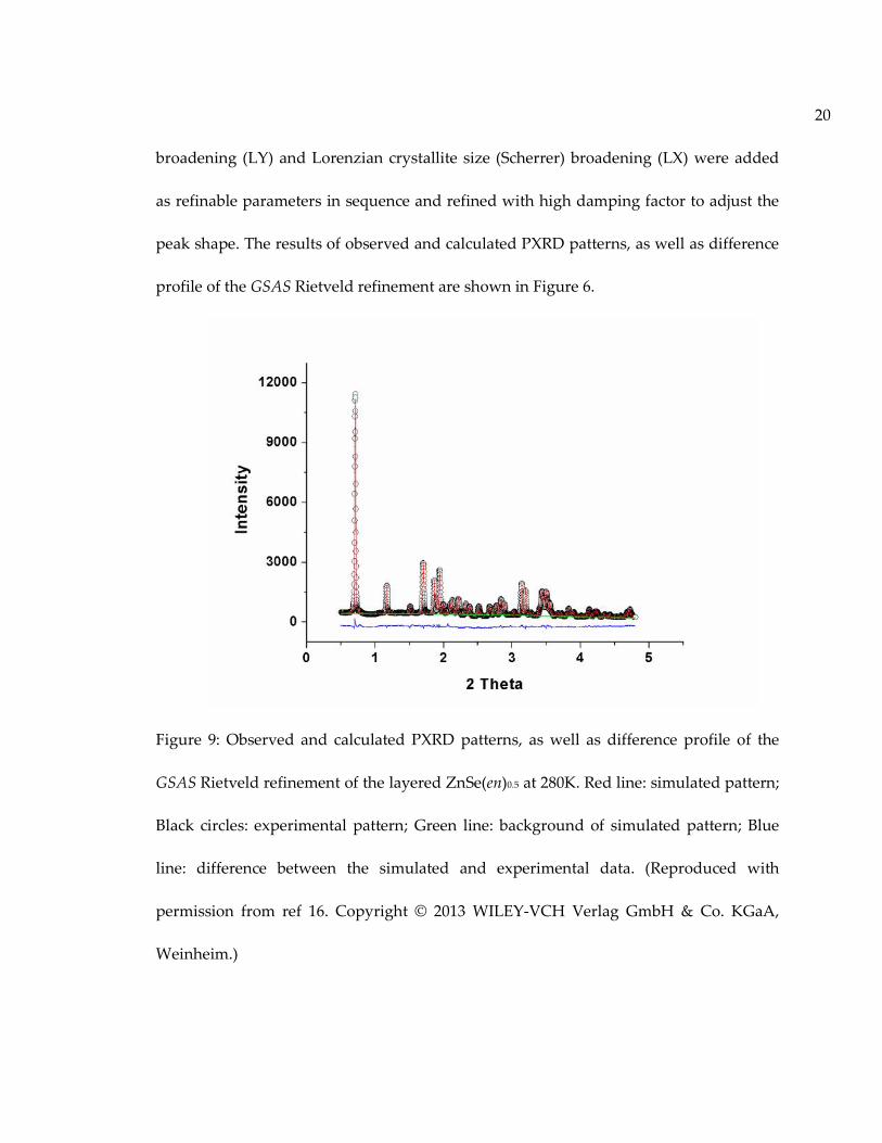
Rietveld analysis based on powder X-ray diffraction data revealed that
ZnSe(en)0.5 compound crystallized in an orthorhombic space group Pbca. There are one
zinc atom, one selenium atom and half ethylenediamine molecule in the crystallographic
asymmetric unit. Each zinc atom connects to three selenium atoms and a nitrogen atom
from ethylenediamine molecule to achieve a stable tetrahedral coordination (Figure 10).
The tellurium atoms coordinated to three zinc atoms. The alternating three-coordinated
Zn and Se atoms form a puckered 63 (distorted honeycomb net) [ZnSe] slab along
crystallographic ab plane. The slabs are interconnected by ethylenediamine molecules
along the c axis through the covalent Zn-N bonds. The Zn-Se bond lengths range from
2.420(4) to 2.460(4) Å (with an average value of 2.443 Å). The Se-Zn-Se bond angles are
115.08/114.22/115.95º, slightly larger than the ideal 109.5º tetrahedral angle.
22
Figure 10: Refined crystal structures of -[ZnSe(en)0.5] (1) (a) viewing from a-axis and (b)
viewing from b-axis The light blue balls are Zn; red balls, Te; blue balls, N; dark grey
balls, C; Hydrogen atoms are omitted for clarity.
Optical diffuse reflectance spectra were measured at room temperature using a
Shimadzu UV-3101PC double monochromated, double beam spectrophotometer. The
absorption edges of ZnSe(en)0.5 are found to be 4.0 eV, indicating a very large blue shift
(1.4-1.6 eV) compared to that of the bulk ZnSe.

23
0 1 2 3 4 50
2
4
6
8
10
12
14
16
KM F
unct
ion
Energy (eV)
Figure 11: Optical absorption spectra of ZnSe(en)0.5 inorganic organic hybrid
semiconductors.

24
2.1.2 3D-ZnSe(pda)0.5 structure
Synthesis of -[ZnSe(pda)0.5] (2). Compound 2 was obtained from the reactions of ZnCl2
(0.273 g, 2 mmol), Se (0.079 g, 1 mmol), and pda (6 mL) in a molar ratio of 2:1:75 in a 23
mL acid digestion bomb at 200 °C for 3 days. The product was washed by distilled water,
ethanol followed by drying in anhydrous ethyl ether. The powders of 2 (0.128 g, 70.0%
based on Se) was isolated.
The crystal structure of -[ZnSe(pda)0.5] was also solved by powder x-ray
diffraction data at 280K. The 280K PXRD data of the powder samples were collected
under helium gas using an Oxford cryomagnet system at the beamline 11-ID-C,
Advanced Photone Source, Argonne National Laboratory. The high-energy synchrotron
X-rays (with a wavelength of 0.1077 Å) were used for the PXRD measurements. The
Rietveld method with the same process stated above was also used to refine the crystal
structure of ZnSe(pda)0.5. To make the refinement results comparable with each other, the
value of zero point was kept same for each compound and for all temperatures. The
Observed and calculated PXRD patterns, as well as difference profile of the GSAS
Rietveld refinement of ZnSe(pda)0.5 at 280K was shown below.74

25
Figure 12: Observed and calculated PXRD patterns, as well as difference profile of the
GSAS Rietveld refinement of the double layered ZnSe(pda)0.5 at 280K. Black circles:
experimental pattern; Red line: simulated pattern; Green line: background of simulated
pattern; Blue line: difference between the experimental and simulated data. (Reproduced
with permission from ref 16. Copyright © 2013 WILEY-VCH Verlag GmbH & Co. KGaA,
Weinheim.)
Compound 2 crystallized in orthorhombic non-centrosymmetric space group
Cmc21. There are one zinc atom, one selenium atom and half pda molecule in the
crystallographic asymmetric unit. Unlike α-ZnTe(en)0.5 (1), in which an crystallographic
inversion center is located in the center of the C-C bond of ethylenediamine molecule,
there is a mirror plane passing through the C2 atom of pda in 2. Consequently, the
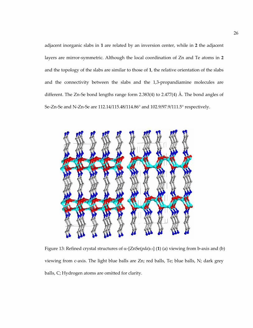
26
adjacent inorganic slabs in 1 are related by an inversion center, while in 2 the adjacent
layers are mirror-symmetric. Although the local coordination of Zn and Te atoms in 2
and the topology of the slabs are similar to those of 1, the relative orientation of the slabs
and the connectivity between the slabs and the 1,3-propandiamine molecules are
different. The Zn-Se bond lengths range form 2.383(4) to 2.477(4) Å. The bond angles of
Se-Zn-Se and N-Zn-Se are 112.14/115.48/114.86° and 102.9/97.9/111.5° respectively.
Figure 13: Refined crystal structures of -[ZnSe(pda)0.5] (1) (a) viewing from b-axis and (b)
viewing from c-axis. The light blue balls are Zn; red balls, Te; blue balls, N; dark grey
balls, C; Hydrogen atoms are omitted for clarity.
27
Optical diffuse reflectance spectra were measured at room temperature on
ZnSe(pda)0.5. The absorption edges of ZnSe(pda)0.5 are found to be 4.0, similar to
ZnSe(en)0.5 indicating a very large blue shift (1.4-1.6 eV) compared to that of the bulk
ZnSe.
0 1 2 3 4 5
0
2
4
6
8
10
KM F
unct
ion
Energy (eV)
Figure 14: Optical absorption spectra of ZnSe(pda)0.5 inorganic organic hybrid
semiconductors.
28
2.1.3 3D-ZnSe(bda)0.5 structure
Synthesis of -[ZnSe(bda)0.5] (3). Compound 3 was prepared from the reactions
of Zn(NO3)2 (0.378 g, 2 mmol), Se (0.079 g, 1 mmol), and bda (6 mL) in a 23 mL acid
digestion bomb. The bomb was sealed and kept at 200 °C for 3 days. The product was
washed by water, ethanol and followed by drying in anhydrous ethyl ether. The
colorless powder of 3 (0.211 g, 82.7% based on Se) was isolated.
The crystal structure of -[ZnSe(bda)0.5] was also solved by powder x-ray
diffraction data at 280K that was collected under synchrotron x-ray diffraction in
Argonne National Laboratory. The Observed and calculated PXRD patterns, as well as
difference profile of the GSAS Rietveld refinement of ZnSe(bda)0.5 at 280K was shown
below.

29
Figure 15: Observed and calculated PXRD patterns, as well as difference profile of the
GSAS Rietveld refinement of the ZnSe(bda)0.5 at 280K. Black circles: experimental pattern;
Red line: simulated pattern; Green line: background of simulated pattern; Blue line:
difference between the experimental and simulated data. (Reproduced with permission
from ref 16. Copyright © 2013 WILEY-VCH Verlag GmbH & Co. KGaA, Weinheim.)
Results from Rietveld analysis shows that it crystallizes in an orthorhombic space
group Pbca, same as ZnSe(bda)0.5 compound. This is reasonable since the relative
direction of electron lone pair in nitrogen atoms are same between 1,2-ethylenediamine
and 1,4-butanediamine, which results in a similar way of packing of inorganic layers in

30
the structure. In the crystallographic asymmetric unit, there are also one zinc atom, one
selenium atom and half organic molecule. Each zinc atom connects to three selenium
atoms and a nitrogen atom from bda molecule to achieve a stable tetrahedral
coordination (Figure 16). The slabs are interconnected by bda molecules along the c axis
through the covalent (dative) Zn-N bonds. The Zn-Se bond lengths range from 2.402(7)
to 2.506(7) Å (with an average value of 2.46 Å). The Se-Zn-Se bond angles are
113.91/115.96/112.00º, slightly larger than the ideal 109.5º tetrahedral angle.
Figure 16: Refined crystal structures of -[ZnSe(bda)0.5] (3) (a) viewing from a-axis and (b)
viewing from b-axis. The light blue balls are Zn; red balls, Te; blue balls, N; dark grey
balls, C; Hydrogen atoms are omitted for clarity.

31
Optical diffuse reflectance spectra were measured at room temperature on
ZnSe(bda)0.5. The absorption edges of ZnSe(bda)0.5 are found to be 4.0, similar to
ZnSe(en)0.5 and ZnSe(pda)0.5 indicating a very large blue shift (1.4-1.6 eV) compared to
that of the bulk ZnSe.
0 1 2 3 4 5
02468
101214161820
Energy (eV)
KM F
unct
ion
Figure 17: Optical absorption spectra of (a) ZnSe(bda)0.5 inorganic organic hybrid
semiconductors
32
2.1.4 3D-ZnSe(ptda)0.5 structure
Synthesis of -[ZnSe(ptda)0.5] (4). Reactions of Zn(NO3)2 (0.378 g, 2 mmol), Se
(0.079 g, 1 mmol), and ptda (6 mL) in a molar ratio of 2:1:75 at 200 °C for 3 days in 23 mL
acid digestion bomb afforded light yellow powders of 4 (0.227 g, 84.0% yield based on
Se). The same experimental procedure used for the synthesis of 1, 2 and 3 was applied
here.
The crystal structure of -[ZnSe(ptda)0.5] was also solved by powder x-ray
diffraction data at 280K and Rietveld refinement was used to get the unit cell, space
group and atomic positions of the compound as for other compounds. The results are
shown below.
Figure 18: Observed and calculated PXRD patterns, as well as difference profile of the
GSAS Rietveld refinement of the ZnSe(ptda)0.5 at 280K. Black circles: experimental

33
pattern; Red line: simulated pattern; Green line: background of simulated pattern; Blue
line: difference between the experimental and simulated data. (Reproduced with
permission from ref 16. Copyright © 2013 WILEY-VCH Verlag GmbH & Co. KGaA,
Weinheim.)
The results from Rietveld analysis reveals that it crystallizes in an
noncentrosymmetric space group Cmc21, same as ZnSe(pda)0.5 compound. This is
reasonable because the relative direction of electron lone pair in nitrogen atoms are same
between 1,3-propanediamine and 1,5-pentanediamine, which results in a similar way of
packing of inorganic layers in the structure. There are one zinc atom, one selenium atom
and half ptda molecule in the crystallographic asymmetric unit. The Zn-Se bond lengths
range from 2.434(9) to 2.459(8) Å (with an average value of 2.436 Å). The Se-Zn-Se bond
angles are 113.62/114.71/113.64º, slightly larger than the ideal 109.5º tetrahedral angle,
while the N-Zn-N bond angles (101.0/ 100.9/111.3º) are slightly compressed.

34
Figure 19: Refined crystal structures of -[ZnSe(ptda)0.5] (1) (a) viewing from b-axis and
(b) viewing from c-axis. The light blue balls are Zn; red balls, Te; blue balls, N; dark grey
balls, C; Hydrogen atoms are omitted for clarity.
Optical diffuse reflectance spectra were measured at room temperature on
ZnSe(ptda)0.5. The absorption edges of ZnSe(ptda)0.5 are found to be 4.0 eV, similar to
other three compounds, indicating a very large blue shift (1.4-1.6 eV) compared to that
of the bulk ZnSe.

35
0 1 2 3 4 5
02468
101214161820
Energy (eV)
KM F
unct
ion
Figure 20: Optical absorption spectra of ZnSe(ptda)0.5 inorganic organic hybrid
semiconductors.
2.1.5 Summary of -ZnSe(L)0.5 inorganic organic hybrid structures
The Rietveld refinement results show that compounds containing organic
diamines with an even number of carbons (n), namely 1 (n = 2) and 3 (n = 4) crystallize in
centrosymmetric space group Pbca (No. 61), and those with organic diamines of an odd
number of carbons, 2 (n = 3) and 4 (n = 5), crystallize in noncentrosymmetric space group
Cmc21 (No. 36). The unit cell parameters of all four structures were refined using full X-
ray diffraction data sets collected at 280 K (see Table 1). The lattice parameters of the
four structures are: -Zn2Se2(en) (1), a = 6.6382(3)Å, b = 6.4702(2) Å, c = 17.3822(6) Å; -

36
Zn2Se2(pda) (2), a = 20.0192(7) Å, b = 6.6389(3) Å, c = 6.4531(2) Å; -Zn2Se2(bda) (3), a =
6.6388(5) Å, b = 6.4662(5) Å, c = 22.3042(13) Å; -Zn2Se2(ptda) (4), a = 25.1159(16) Å, b =
6.6218(6) Å, c = 6.4436(5) Å. As the number of carbon atoms increases, the length of the
long axis (L3) increases by about 2.5 Å per carbon atom, while the length of other two
short axes (L1 and L2) remains approximately the same.

37
Table 2: Crystal structure data of α-ZnSe(en)0.5 (1),α- ZnSe(pda)0.5 (2),α-ZnSe(bda)0.5
(3),and α-ZnSe(ptda)0.5 (4) by Rietveld refinement. (Reproduced with permission fromref 16. Copyright © 2013 WILEY-VCH Verlag GmbH & Co. KGaA, Weinheim.)
Empirical
Formula
ZnSe (en)0.5 ZnSe(pda)0.5 ZnSe(bda)0.5 ZnSe(ptda)0.5
Fw 348.83 362.83 376.85 390.98
Space
Group
Pbca Cmc21 Pbca Cmc21
a (Å) 6.6382(3)
(L1)
20.0192(7)
(L3)
6.6388(5)
(L1)
25.1159(16)
(L3)
b (Å) 6.4702(2)
(L2)
6.6389(3)
(L1)
6.4662(5)
(L2)
6.6218(6)
(L1)
c (Å) 17.3822(6)
(L3)
6.4531(2)
(L2)
22.3042(13)
(L3)
6.4436(5)
(L2)
V (Å3) 746.58(5) 857.65(6) 957.48(12) 1071.65(14)
Z 8 8 8 8
T (K) 280 280 280 280
(Å) 0.107716 0.107716 0.107716 0.107716
(g∙cm-3) 3.103 2.810 2.61 2.42
2range 0.45-4.8 0.45-4.8 0.45-4.8 0.45-4.8

38
The atomic coordinates and equivalent isotropic temperature factors and structural
refinement information of 1, 2, 3 and 4 at 280K were shown in the following Table 2 and
the selected bond lengths (Å) and angles (deg) of the structures 1, 2, 3 and 4 are shown
in Table 3, 4, 5 and 6, respectively.
Table 3: Atomic Coordinates and Equivalent Isotropic Temperature Factors (Å2) for 1, 2,
3 and 4 at 280K. Hydrogen atoms are omitted. (Reproduced with permission from ref 16.
Copyright © 2013 WILEY-VCH Verlag GmbH & Co. KGaA, Weinheim.)
atoms x y z Ueq
1
Zn 0.1009(4) 0.1494(5) 0.2976(2) 0.0219(7)
Se 0.4452(4) 0.0212(4) 0.3189(1) 0.0144(5)
()
Step size
(2)
0.0015 0.0015 0.0015 0.0015
Step scan
time (s)
8 8 8 8
Rwp 0.0600 0.0616 0.0684 0.0736
Rp 0.0410 0.0442 0.0503 0.0542

39
N -0.0373(21) 0.0213(25) 0.3925(7) 0.0290(6)
C1 0.0408(30) 0.0640(30) 0.4691(10) 0.0290(10)
2
Zn1 0.2100(2) 0.1573(4) 0.0525(5) 0.0301(8)
Se 0.1901(1) 0.1904(3) 0.4277(5) 0.0147(5)
N 0.1218(6) 0.2970(23) -0.0819(30) 0.0151(1)
C1 0.0563(8) 0.2325(29) -0.0131(1) 0.0131(1)
C2 0.0000(0) 0.3030(4) -0.1020(1) 0.0201(1)
3
Zn -0.0915(8) 0.3043(8) 0.28767(23) 0.0450(15)
Se -0.0583(6) -0.0616(7) 0.30346(17) 0.0246(9)
N 0.0441(4) 0.4251(5) 0.3613(8) 0.0221(0)
C1 -0.0290(4) 0.3910(7) 0.4211(10) 0.0342(2)
C2 0.0441(6) 0.519(7) 0.4729(12) 0.0401(2)
4
Zn 0.2168(2) 0.1547(9) 0.2309(9) 0.0463(16)
Se 0.2026(5) 0.1909(7) 0.6028(10) 0.0232(10)
N 0.1506(8) 0.297(4) 0.1171(5) 0.0241(2)
C1 0.0996(11) 0.2331(1) 0.1811(7) 0.0412(2)
C2 0.0516(11) 0.3221(1) 0.0821(1) 0.036(18)
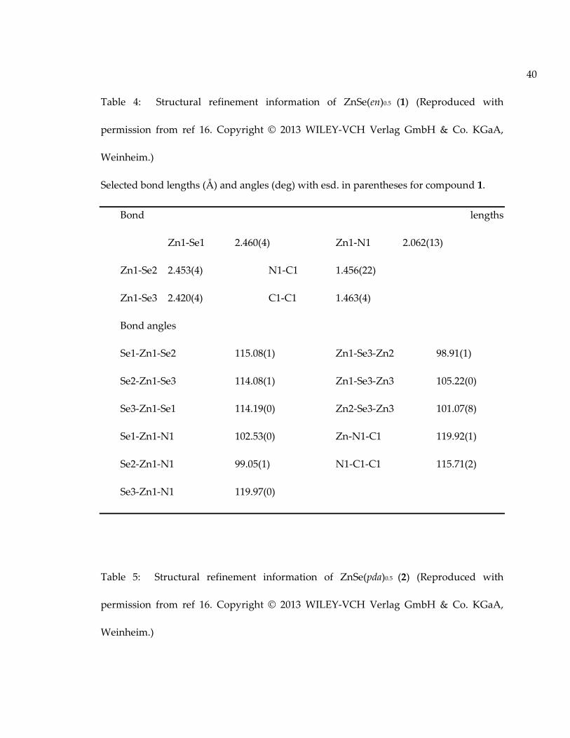
40
Table 4: Structural refinement information of ZnSe(en)0.5 (1) (Reproduced with
permission from ref 16. Copyright © 2013 WILEY-VCH Verlag GmbH & Co. KGaA,
Weinheim.)
Selected bond lengths (Å) and angles (deg) with esd. in parentheses for compound 1.
Bond lengths
Zn1-Se1 2.460(4) Zn1-N1 2.062(13)
Zn1-Se2 2.453(4) N1-C1 1.456(22)
Zn1-Se3 2.420(4) C1-C1 1.463(4)
Bond angles
Se1-Zn1-Se2 115.08(1) Zn1-Se3-Zn2 98.91(1)
Se2-Zn1-Se3 114.08(1) Zn1-Se3-Zn3 105.22(0)
Se3-Zn1-Se1 114.19(0) Zn2-Se3-Zn3 101.07(8)
Se1-Zn1-N1 102.53(0) Zn-N1-C1 119.92(1)
Se2-Zn1-N1 99.05(1) N1-C1-C1 115.71(2)
Se3-Zn1-N1 119.97(0)
Table 5: Structural refinement information of ZnSe(pda)0.5 (2) (Reproduced with
permission from ref 16. Copyright © 2013 WILEY-VCH Verlag GmbH & Co. KGaA,
Weinheim.)
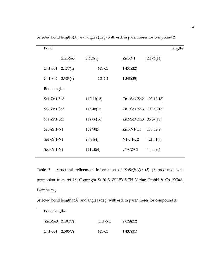
41
Selected bond lengths(Å) and angles (deg) with esd. in parentheses for compound 2:
Bond lengths
Zn1-Se3 2.463(5) Zn1-N1 2.174(14)
Zn1-Se1 2.477(4) N1-C1 1.451(22)
Zn1-Se2 2.383(4) C1-C2 1.348(25)
Bond angles
Se1-Zn1-Se3 112.14(15) Zn1-Se3-Zn2 102.17(13)
Se2-Zn1-Se3 115.48(15) Zn1-Se3-Zn3 103.57(13)
Se1-Zn1-Se2 114.86(16) Zn2-Se3-Zn3 98.67(13)
Se3-Zn1-N1 102.90(5) Zn1-N1-C1 119.02(2)
Se1-Zn1-N1 97.91(4) N1-C1-C2 121.51(3)
Se2-Zn1-N1 111.50(4) C1-C2-C1 113.32(4)
Table 6: Structural refinement information of ZnSe(bda)0.5 (3) (Reproduced with
permission from ref 16. Copyright © 2013 WILEY-VCH Verlag GmbH & Co. KGaA,
Weinheim.)
Selected bond lengths (Å) and angles (deg) with esd. in parentheses for compound 3:
Bond lengths
Zn1-Se3 2.402(7) Zn1-N1 2.029(22)
Zn1-Se1 2.506(7) N1-C1 1.437(31)

42
Zn1-Se2 2.423(7) C1-C2 1.503(5)
C2-C2 1.371(6)
Bond angles
Se1-Zn1-Se3 113.91(25) Zn1-Se3-Zn2 103.59(21)
Se2-Zn1-Se3 115.96(25) Zn1-Se3-Zn3 105.50(1)
Se1-Zn1-Se2 112.00(25) Zn2-Se3-Zn3 98.00(1)
Se3-Zn1-N1 102.62(8) Zn1-N1-C1 122.91(21)
Se1-Zn1-N1 99.61(7) N1-C1-C2 121.41(31)
Se2-Zn1-N1 110.94(9) C1-C2-C2 116.00(20)
Table 7: Structural refinement information of ZnSe(ptda)0.5 (4) (Reproduced with
permission from ref 16. Copyright © 2013 WILEY-VCH Verlag GmbH & Co. KGaA,
Weinheim.)
Selected bond lengths(Å) and angles (deg) with esd. in parentheses for compound 4:
Bond lengths
Zn1Se3 2.434(9) N1-C1 1.412(4)
Zn1-Se1 2.459(8) C1-C2 1.481(5)
Zn1-Se2 2.415(8) C2-C3 1.502(4)
Zn1-N1 2.054(25)

43
Bond angles
Se2-Zn1-Se3 113.62(29) Zn1-Se3-Zn2 102.57(25)
Se2-Zn1-Se3 114.71(29) Zn1-Se3-Zn3 104.78(24)
Se1-Zn1-Se2 113.67(30) Zn2-Se3-Zn3 99.06(24)
Se3-Zn1-N1 100.91(10) Zn1-N1-C1 119.61(25)
Se1-Zn1-N1 101.02(9) N1-C1-C2 119.62(35)
Se2-Zn1-N1 111.31(8) C1-C2-C3 114.02(4)
C2-C3-C2 119.02(30)

44
2.2 Thermal expansion behavior of ZnSe(L) hybrid structures
2.2.1 Significance of thermal expansion behavior study
Most materials in nature expand on heating, a phenomenon referred to as positive
thermal expansion (PTE). The opposite behavior occurs less commonly, when materials
shrink upon heating, and is called negative thermal expansion (NTE).75,76 Several
possible mechanisms may be associated with the negative thermal expansion found in
oxide phases. First of all, the metal oxygen polyhedron becomes less distorted with
increasing temperature and the higher regularity can lead to shorter bond length and
lead to negative thermal expansion. For example, the distorted TiO6 octahedron in
BaTiO377 and PbTiO378 become more regular upon heating which leads to NTE in a
certain temperature range. Secondly, the distribution of interstitial cations in some open
structures such as -eucryptite79, named after a mineral LiAlSiO4, may vary over
available sites with changing temperature. In such a case, the increase in the Li-O bond
length drives the thermal expansion in two dimensions while the rigidity of the Al-O
and Si-O bonds forces the contraction in the third dimension. Thirdly, rotation of a metal
oxygen polyhedra can also trigger anisotropic NTE. This mechanism was first found in
cordierite Mg2Al2Si5O1813, where the increase of the Mg-O bond length within the two
dimensional slab causes the expansion of the slab as temperature rises. However, the
lengths of the Si-O or Al-O bonds between the slabs are not affected, and the changes in
the bond angles of the SiO4 or AlO4 tetrahedron rotate the polyhedron in such a way that

45
pulls the slabs closer together, resulting in negative thermal expansion in the direction
perpendicular to the slabs. In addition to the NTE mechanisms mentioned above, the
transverse thermal motion (TTM) is also a well-accepted and common mechanism for
NTE80,81. In such a case, NTE originates from the transverse thermal vibration of bridging
cyanide or oxide ions which draw their connected metal centers closer together (i.e.
AM2O882,83, AM2O784, A2M3O1285, zeolite86, M(CN)287, ReO388,89 families and Prussian blue
analogues90-92), resulting in the observed contraction of the lattice parameter as a
function of increasing temperature.
One of the important applications of NTE compounds is their use in fabrication of
composite materials having an overall zero thermal expansion (ZTE). With a constant
volume, the ZTE composite neither expand nor contract as temperature changes. These
materials are highly desirable because they are free of thermal shock on rapid
temperature change, and can prevent structural instability and mechanical degradation
caused by the fragility of ceramics towards sizable and volumetric changes as
temperature varies93,94. A common approach to achieve an overall zero thermal
expansion is to blend a PTE and a NTE material. However, this method remains to be a
major technical challenge due to the incompatibility of the two very different phases.95
Furthermore, in such ZTE composites, the PTE ingredient often shows quite different
thermal behavior from that of the NTE ingredient as temperature varies. Hence, the
stress induced at interfaces may give rise to microcracks, which degrade the mechanical
46
performance and sometimes physical properties.96 Such a microcracking problem may
be avoided if zero thermal expansion can be achieved in a single crystalline material.
The structures with such properties are also rare. Most of them reported till present are
insulating oxides which have found use in heat-engine components, optics and
kitchenwares, but are not suitable for applications in optoelectronics and electronics.
Very few known examples of non-oxide ZTE materials that exhibit semiconductive or
conductive properties include metallic Invar Fe-Ni alloys (Fe36Ni)95, Mn3Cu1-xSixGexN96
and YbGaGe97.
Crystalline inorganic organic hybrid semiconductors are a new type of functional
materials that incorporate semiconductor modules in nanoscale and organic molecules
in a single crystal lattice.15,98-105 Study on a prototype -3D-ZnTe(en)0.5 structure revealed
that both ZnTe and ethylenediamine molecule show typical PTE, however their hybrid
structure exhibits nearly zero thermal expansion along the layer stacking axis.104
Specifically, the inorganic component (ZnTe slab) remains to be PTE but the organic
diamine shows strong NTE in the hybrid structure. This study suggests that hybrid
structures may have the following advantages as possible candidates for ZTE materials:
(a) ZTE may be achieved by the two opposing effect (NTE and PTE) within a single
crystal lattice to avoid grain boundary associated cracks, and (b) Both PTE and NTE can
be systematically and independently tuned by varying the inorganic layers and organic
molecules.

47
Based on these considerations, we have carried out a systematic study of the thermal
expansion behavior on a series of 3D--ZnSe(L)0.5 type compounds, an analogue of the
3D--ZnTe(en)0.5 and 3D--ZnTe(L)0.5 hybrid structures.15 We report the synthesis and
structure refinement of -[ZnSe(en)0.5] (1), -[ZnSe(pda)0.5] (2), -[ZnSe(bda)0.5] (3), and -
[ZnSe(ptda)0.5] (4) (where - and -phase have very similar structures, with only small
differences in the bond distances and angles in the inorganic layer).
2.2.2 Thermal expansion results and analysis.
In order to study the thermal expansion behavior of -ZnSe(L)0.5, the PXRD
patterns of the powder samples were collected between 5K and 300K at an interval of 10
K under helium gas using an Oxford cryomagnet system at the beamline 11-ID-C,
Advanced Photone Source, Argonne National Laboratory. The high-energy synchrotron
X-rays (with a wavelength of 0.1077 Å) were used for the PXRD measurements. The
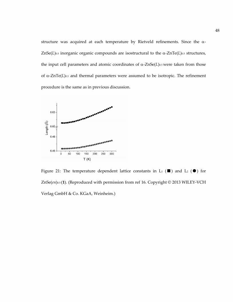
48
structure was acquired at each temperature by Rietveld refinements. Since the -
ZnSe(L)0.5 inorganic organic compounds are isostructural to the -ZnTe(L)0.5 structures,
the input cell parameters and atomic coordinates of -ZnSe(L)0.5 were taken from those
of -ZnTe(L)0.5 and thermal parameters were assumed to be isotropic. The refinement
procedure is the same as in previous discussion.
Figure 21: The temperature dependent lattice constants in L1 (■ ) and L2 (●) for
ZnSe(en)0.5 (1). (Reproduced with permission from ref 16. Copyright © 2013 WILEY-VCH
Verlag GmbH & Co. KGaA, Weinheim.)

49
Figure 22: The temperature dependent lattice constants in L1 (■ ) and L2 (●) for
ZnSe(pda)0.5 (2). (Reproduced with permission from ref 16. Copyright © 2013 WILEY-
VCH Verlag GmbH & Co. KGaA, Weinheim.)
Figure 23: The temperature dependent lattice constants in L1 (■ ) and L2 (●) for
ZnSe(bda)0.5. (Reproduced with permission from ref 16. Copyright © 2013 WILEY-VCH
Verlag GmbH & Co. KGaA, Weinheim.)
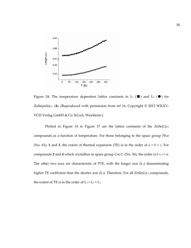
50
Figure 24: The temperature dependent lattice constants in L1 (■ ) and L2 (●) for
ZnSe(ptda)0.5 (4). (Reproduced with permission from ref 16. Copyright © 2013 WILEY-
VCH Verlag GmbH & Co. KGaA, Weinheim.)
Plotted in Figure 14 to Figure 17 are the lattice constants of the ZnSe(L)0.5
compounds as a function of temperature. For those belonging to the space group Pbca
(No. 61), 1 and 3, the extent of thermal expansion (TE) is in the order of a > b > c. For
compounds 2 and 4 which crystallize in space group Cmc21 (No. 36), the order is b > c > a.
The other two axes are characteristic of PTE, with the longer axis (L1) demonstrating
higher TE coefficient than the shorter axis (L2). Therefore, For all ZnSe(L)0.5 compounds,
the extent of TE is in the order of L3 < L2 < L1.

51
Figure 25: The temperature dependent lattice constants in L3 for (up) ZnSe(en)0.5 (1) ()
and ZnSe(pda)0.5 (2) (); (down) ZnSe(bda)0.5 (3) () and ZnSe(ptda)0.5 (4)
().(Reproduced with permission from ref 16. Copyright © 2013 WILEY-VCH Verlag
GmbH & Co. KGaA, Weinheim.)

52
Using lattice parameters obtained at different temperatures, the linear thermal
expansion coefficients (L or simply ) can be calculated with formula :
where L is the lattice constant and dL/dT is the rate of change of lattice constant
per unit change in temperature. The calculated thermal expansion coefficients for all
four compounds are included in Table 8.
Table 8: Linear thermal expansion coefficients () of 1 - 4. (Reproduced with permission
from ref 16. Copyright © 2013 WILEY-VCH Verlag GmbH & Co. KGaA, Weinheim.)
To compare the relative expansion behaviors of different axis over the whole
temperature range, the normalized lattice constants, a, b and c are calculated by dividing
the change in length during the thermal expansion by the length at 5K (L/L0) for the
four compounds and the results are plotted in Figure 26 to Figure 29. For all four
Compound 106/K-1
(L3)
106/K-1
(L1)
106/K-1
(L2)
ZnSe(en)0.5 (1) 3.39 17.4 9.04
ZnSe(bda)0.5 (3) 3.56 20.5 10.1
ZnSe(pda)0.5 (2) 3.32 18.9 12.2
ZnSe(ptda)0.5 (4) -0.78 23.1 15.6

53
compounds, the long axis (L3) displays the least thermal expansion with their TE
coefficients less than 510-6/K (See Table 8), indicating nearly ZTE in this direction.
Figure 26: The normallized lattice constants L1(■), L2(●)and L3(▲) for -ZnSe(en)0.5 (1)
at different temperatures. (Reproduced with permission from ref 16. Copyright © 2013
WILEY-VCH Verlag GmbH & Co. KGaA, Weinheim.)

54
Figure 27: The normallized lattice constants L1(■), L2(●)and L3(▲) for -ZnSe(pda)0.5
(2), at different temperatures. (Reproduced with permission from ref 16. Copyright ©
2013 WILEY-VCH Verlag GmbH & Co. KGaA, Weinheim.)
Figure 28: The normallized lattice constants L1(■), L2(●)and L3(▲) for-ZnSe(bda)0.5
(3) at different temperatures. (Reproduced with permission from ref 16. Copyright ©
2013 WILEY-VCH Verlag GmbH & Co. KGaA, Weinheim.)
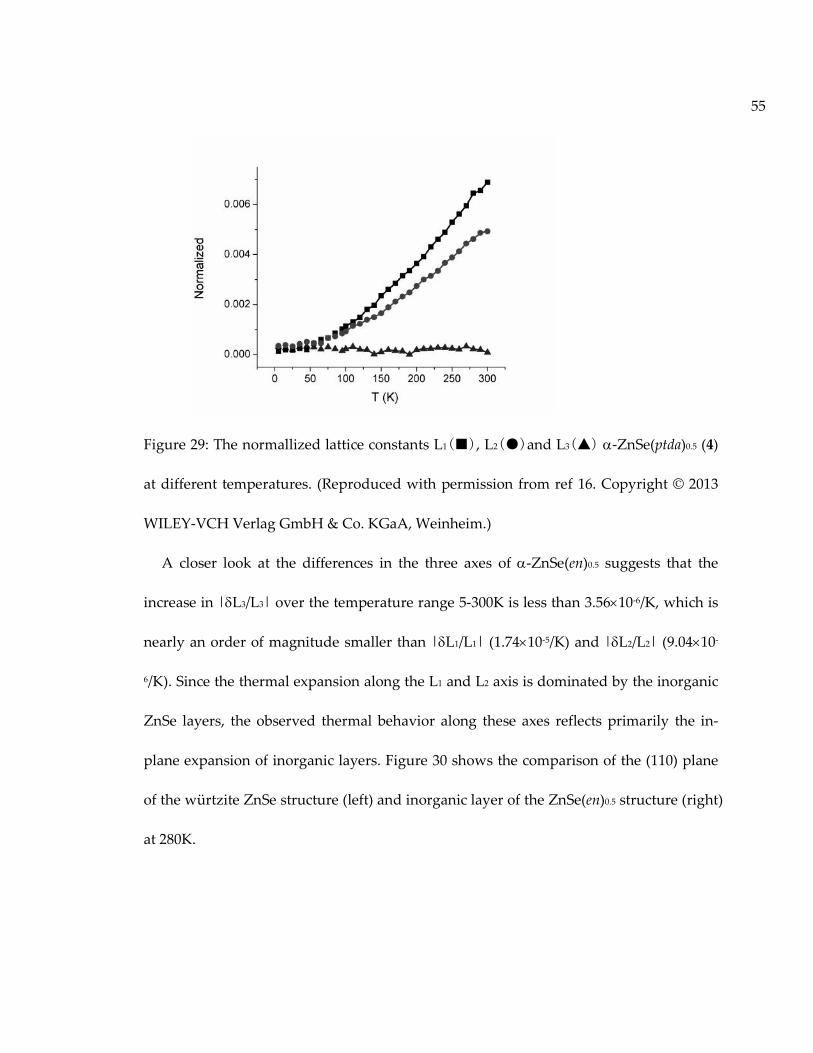
55
Figure 29: The normallized lattice constants L1(■), L2(●)and L3(▲) -ZnSe(ptda)0.5 (4)
at different temperatures. (Reproduced with permission from ref 16. Copyright © 2013
WILEY-VCH Verlag GmbH & Co. KGaA, Weinheim.)
A closer look at the differences in the three axes of -ZnSe(en)0.5 suggests that the
increase in |L3/L3| over the temperature range 5-300K is less than 3.5610-6/K, which is
nearly an order of magnitude smaller than |L1/L1| (1.7410-5/K) and |L2/L2| (9.0410-
6/K). Since the thermal expansion along the L1 and L2 axis is dominated by the inorganic
ZnSe layers, the observed thermal behavior along these axes reflects primarily the in-
plane expansion of inorganic layers. Figure 30 shows the comparison of the (110) plane
of the würtzite ZnSe structure (left) and inorganic layer of the ZnSe(en)0.5 structure (right)
at 280K.

56
Figure 30: Comparison of a single (110) plane of the würtzite ZnSe (left) and a single
inorganic slab of ZnSe(en)0.5 (right). The L1 and L2 axes of the ZnSe(en)0.5 structure are a
and b, respectively. Zn: grey balls; Te: black balls. (Reproduced with permission from ref
16. Copyright © 2013 WILEY-VCH Verlag GmbH & Co. KGaA, Weinheim.)
As shown in the figure 30, the L2 axis in the ZnSe(en)0.5, with the cell parameter L2 = b
= 6.47 Å, can be related to the [001] (or c) axis of the hexagonal ZnSe structure, with the
value of c = 6.50 Å at room temperature. Thus, the ZnSe(en)0.5 hybrid structure shows
about 0.5% compression compared to the parent ZnSe structure along this direction. Its
L1 (or a) axis can be related to the [1-10] direction in ZnSe parent structure (6.88 Å). With
a length of 6.64 Å, L1 exhibits a compression of ~4% along this direction, significantly
higher than that along L2. The stronger distortion in the L1 axis is apparent as shown in
Figure 27. It appears that the more compressed L1 axis is more likely to expand to release
the strain and thus a higher thermal expansion coefficient of |L1/L1| = 1.7410-5/K.
While for the less compressed L2 axis, a lower thermal expansion coefficient |L2/L2| =
57
9.0410-6/K, close to the thermal expansion coefficient of 8.4710-6/K of the ZnSe würtzite
structure in the same temperature range, is obtained.
A comparison of the thermal expansion behavior of short axes (L1 and L2) among all
four compounds reveals some interesting findings. In general, as the number of carbon
atoms increases from 1 to 4, the thermal expansion coefficient of L1 axis increase
sequentially: 1 (17.410-6) < 2 (18.910-6) < 3 (20.510-6) < 4 (23.110-6) (see Table 8). Similar
trend is also observed in the L2 axis. The TE coefficient increases are in the order of: 1
(9.0410-6) < 3 (10.110-6) and 2 (12.210-6) < 4 (15.610-6). Note the extent of increase is
different for compounds with even and odd number of carbons. The thermal expansion
behaviors of the title compounds-ZnSe(L)0.5 are also compared with their ZnTe
analogues -ZnTe(L)0.5.28 For the ZnTe(L)0.5 structures the extent of thermal expansion
(measured on single crystals) is in the order of L1, L2, and L3, in agreement with the
thermal expansion trend of -ZnSe(L)0.5 powders. The two short axes that are parallel to
the inorganic layers respond positively to the increase of temperature and their thermal
expansion coefficients varying between (1.4-2.9)10-5 K-1 and (0.9-1.5)10-5 K-1 for L1 and
L2, respectively, in the temperature range of 95-295K. These values are comparable to
those of the corresponding ZnSe(L)0.5 phases, (1.74-2.31)10-5 K-1 and (0.90-1.56)10-5 K-1
for L1 and L2 (5-300K). For L3, the ranges for four different compounds are (-0.78-
3.56)10-6 K-1. Therefore, both -ZnTe(L)0.5 and -ZnSe(L)0.5 materials show anisotropic
thermal expansion behavior with the same trends of L1 > L2 > L3. Compared to the short

58
axes L1 and L2 that reflect the TE behavior of the inorganic layers only, the thermal
expansion behavior of L3 axis, which is perpendicular to the ZnSe layers, is a combined
effect of both the organic and inorganic component. For compounds 1 and 3 with
centrosymmetic space group Pbca, the thermal expansion coefficients of the c-axis (L3)
are similar (3.3910-6 and 3.5610-6 K-1 for 1 and 3, respectively, indicating the nearly zero
thermal expansion along this axis. For compounds 2 and 4 crystallized in
noncentrosymmetric space group Cmc21, the thermal expansion coefficients of the a-axis
(L3) are very different, with a PTE for 2 (3.3210-6/K) and a NTE for 4 (-7.810-7/K). The
latter value is among the smallest values reported to date, for instance -510-7 for
Mn3(Ga0.5Ge0.4Mn0.1)(N1−xCx)20 and 5.610-7 for (1-x)PbTiO3–xBi(Mg,Ti)1/2O334. The
observed trend along the L3 axis is similar to that of the -ZnTe(L)0.5 (L = hz, en, pda, bda
and ptda) compounds, which also display a conversion from small PTE to NTE as the
number of carbon atoms in the diamine molecules reaches to a certain level (n = 2).
To better understand the negative thermal expansion effect in the organic diamine
molecules, we examined the structures of ZnSe(ptda)0.5 at 5K and 280K closely and
compared the related bond lengths and angles in detail (see Figure 31). Clearly, all
individual bond lengths in the organic amine (ptda) show normal PTE effect, and thus,
they are not the reason for the observed NTE effect. The shortest H∙∙∙∙H distances (the
distance between the two H atoms in the two nearest neighboring ptda molecules) are
similar in both structures at 5 and 280K, with values of 3.456 Å and 3.468 Å at 5 and

59
280K, respectively. If the length of ptda is kept unchanged going from 280 to 5K, the
above H∙∙∙∙H distance would become significantly shorter than those in the structures at
5 and 280K. To avoid the crowded packing, the molecule stretches out along its chain
axis, which is accompanied by an increase in all C-C-N and C-C-C angles. This in turn
results in a negative thermal expansion effect on organic diamine.

60
Figure 31: Bond distances and angles of ptda in the ZnSe(ptda)0.5 structure at 280K (top )
and 5K (bottom). The closest distances between the two H atoms of the neighboring ptda
are 3.468 and 3.456Å at 280 and 5K, respectively. View is along L2 or c-axis. (Reproduced
with permission from ref 16. Copyright © 2013 WILEY-VCH Verlag GmbH & Co. KGaA,
Weinheim.)
61
2.3 Summary
In summary, we have prepared and structurally characterized a group of inorganic-
organic hybrid semiconducting materials with general formula ZnSe(L)0.5. The thermal
expansion coefficients along the layer stacking (L3) axis are between -1 10-6 and 4 10-6
K-1 in the temperature range between 5K and 300K for all four structures, indicating a
nearly-zero linear thermal expansion in the direction. A very small negative thermal
expansion coefficient of -7.810-7 K-1 is achieved for ZnSe(ptda)0.5 along the L3 axis, which
is among the smallest values reported to date (5.610-7 for (1-x)PbTiO3–xBi(Mg,Ti)1/2O3
and -510-7 for Mn3(Ga0.5Ge0.4Mn0.1)(N1−xCx)). The NTE effect observed in the organic
diamines is a structural response to maintain a stable geometry as the PTE changes take
place in the inorganic layers. Since the length of both the organic and inorganic layers
can be independently varied, these hybrid structures have the capability to
systematically tune the thermal expansion properties at a large scale.

62
3. VI-VI inorganic organic hybrid semiconductors
3.1 MO3(L)(L= organic ligand) structures
Inspired by the success with the II-VI chalcogenide derived hybrid
semiconductors, we looked further into important oxide semiconductors as parent
structures for new hybrid systems. The WO3 and MoO3 semiconductors and their
derivatives have been extensively studied owing to their unusual electric, optic and
thermal properties with many potential applications.17,18 For example, WO3 have widely
been studied in photochemical water oxidation and dye-sensitized solar cell due to its
desired band structure, to further increase water oxidation efficiency and photoelectric
conversion efficiency, people have made great efforts in adjusting the band gap and femi
level by making nanostructures or doping in WO3.33-35 In addition, scientists dealing with
energy issue have considered MoO3 and WO3 as good candidates for lithium ion battery
and electrochromic window due to their high lithium ion capacity and outstanding
coloration efficiency.57,106 Both of the applications require fast lithium ion
intercalation/deintercalation process and layered structures with large surface/volume
ratio are always desired. Furthermore, MoO3 were also combined with polymers to
make composite thermoelectric source. 67 By increasing the interface induced phonon
scattering, the thermoconductivity is apparently reduced, which is the most important
approach to increase figure of merit in thermoelectrics. Based on facts and
considerations stated above, we have designed a novel system of MO3(L) (L=organic

63
linker) that contain 1D, 2D and 3D periodically ordered nanostructures under mild
solvothermal conditions. By inserting different neutral organic linkers inside the parent
MO3 perovskite structure, the tunable band structures, the chainlike and layered
inorganic VI-VI structural motifs and the desired interfaces between inorganic and
organic layers can be achieved.
3.1.1 3D-MO3(L)(L= organic ligand) structures
3.1.1.1 3D-MoO3(pyz)0.5 (pyz = pyrazine)
3D-MoO3(pyz)0.5 (pyz = pyrazine)] (1) was prepared from the reactions of MoO3
(0.16 g), CuCl2·2H2O (0.10 g), pyrazine (0.22g) and 10 ml H2O in a 23 mL acid digestion
bomb at 160 °C for 5d. The dark blue powders were washed with water and 95% ethanol
and then heated in the air at 150ºC for 12h. The orange powder of 1 was collected in 50%
yield based on MoO3.107
3D-MoO3(pyz)0.5 crystallizes in a non-centrosymmetric space group I222. The
structure of 1 consists of layers of corner-sharing 108 octahedra parallel to the ab plane
linked through pyrazine molecules into a 3D molybdenum oxide/pyz chiral framework.
The 3D architecture of 1 can be described as an interwoven net of inorganic metal oxide
layers linked by organic tethers. The molybdenum oxide layers are stacked along the c
axis alternatively in an ABAB…sequence. One-dimensional rectangular channels along
the b axis circumscribed by six 108 octahedra and two pyz molecules are as a result of the
connectivity between the molybdenum oxide layers and pyrazine molecules.

64
Molybdenum atoms coordinate with one terminal oxo group, four bridging oxo groups
and one pyz nitrogen donor with Mo–O bond lengths of 1.681(3), 2×1.923(3), 2×1.929(3)
Å and the Mo–N length of 2.483(3) Å. This geometry is different from the common ‘two
short–two intermediate–two long’ bond length pattern of molybdenum oxides. The
significant lengthening in the Mo–N distance is caused by the strong trans effects of the
terminal oxo group. The carbon atom of organic linker is distorted, and the fourfold
crystal symmetry of 1 is prevented.
(a) (b)
Figure 32: A view of the structure of 3D-MoO3(pyz)0.5 through (a) a-axis and (b) c-axis.
65
3.1.1.2 3D-WO3(pyz)0.5 (pyz = pyrazine)
3D-WO3(pyz)0.5 (pyz = pyrazine)] (2) was prepared from the reactions of W(0.072g),
3Na2WO4·9WO3·H2O (0.36 g), pyrazine (0.072 g) and 8 ml H2O in a 23 mL acid digestion
bomb at 150 °C for 7 days. After systematic cooling with the speed of 0.1 °C /min to
room temperature, dark blue black crystals of 2 were collected by vacuum filtration and
dried (yield ca. 50% based on 3Na2WO4·9WO3·H2O).109
The structure of WO3(pyz)0.5 crystallizes in tetrahedral lattice with the space
group of I4/mmm. Though the symmetry of compound 2 is different from 1, the
structures of compounds are still very similar. WO3(pyz)0.5 2 also consists of layers of
corner sharing {WO5N} octahedra parallel to the ab-plane linked through pyrazine
molecules into a 3D tungsten oxide/pyz framework. The tungsten oxide layers are
stacked along the c axis alternatively in an ABAB… sequence. One-dimensional
rectangular channels along the b axis circumscribed by six {WO5N}octahedra and two
pyz molecules are as a result of the connectivity between the tungsten oxide layers and
pyrazine molecules. The size of the channels is about 7.7 × 5.2 Å. Tungsten atoms
coordinate with one terminal oxo group, four bridging oxo groups and one pyz nitrogen
donor with W–O bond lengths of 1.680(2), 4 × 1.8741(3) Å and W–N bond length of
2.440(3) Å.
The experimental XRD pattern of the as-prepared WO3(pyz)0.5 matches pretty
well with its simulated pattern, indicating the pure phase of the resulted compound.
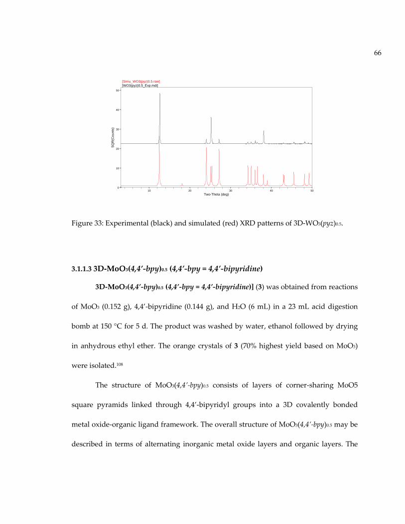
66
Figure 33: Experimental (black) and simulated (red) XRD patterns of 3D-WO3(pyz)0.5.
3.1.1.3 3D-MoO3(4,4’-bpy)0.5 (4,4’-bpy = 4,4’-bipyridine)
3D-MoO3(4,4’-bpy)0.5 (4,4’-bpy = 4,4’-bipyridine)] (3) was obtained from reactions
of MoO3 (0.152 g), 4,4’-bipyridine (0.144 g), and H2O (6 mL) in a 23 mL acid digestion
bomb at 150 °C for 5 d. The product was washed by water, ethanol followed by drying
in anhydrous ethyl ether. The orange crystals of 3 (70% highest yield based on MoO3)
were isolated.108
The structure of MoO3(4,4’-bpy)0.5 consists of layers of corner-sharing MoO5
square pyramids linked through 4,4’-bipyridyl groups into a 3D covalently bonded
metal oxide-organic ligand framework. The overall structure of MoO3(4,4’-bpy)0.5 may be
described in terms of alternating inorganic metal oxide layers and organic layers. The
10 20 30 40 50Two-Theta (deg)
0
10
20
30
40
50
SQ
R(C
ount
s)
[WO3(pyz)0.5_Exp.mdi][Simu_WO3(pyz)0.5.raw]

67
distorted MoO5N coordination geometry at each Mo site is defined by a terminal oxo
group, four asymmetrically bridging oxo groups, and a pyridyl nitrogen group and has
the typical “two short, two intermediate, and two long” bond length geometry which is
common to MoO3. The long Mo-N distances, 2.412(6) Å, reflect the strong trans influence
of the terminal oxo group. This phenomenon has also been observed in structure 1 and 2.
The terminal Mo-O bond distances is 1.698(5) Å, and the bridging Mo-O bond distances,
range from 1.763(5) to 2.120(5) Å. These numbers are within the range expected for
molybdenum oxides.
(a) (b)

68
(c)
Figure 34: A view of the structure of 3D-MoO3(4,4’-bpy)0.5 through (a) a-axis, (b) b-axis
and (c) c-axis.
The experimental XRD pattern of the as-prepared MoO3(4,4’-bpy)0.5 matched
pretty well with its simulated pattern, indicating the pure phase of the resulted
compound.

69
Figure 35: Experimental (black) and simulated (red) XRD patterns of 3D-MoO3(4,4’-
bpy)0.5.
3.1.1.4 3D-WO3(4,4’-bpy)0.5 (4,4’-bpy = 4,4’-bipyridine)
Synthesis of 3D-WO3(4,4’-bpy)0.5 (4,4’-bpy = 4,4’-bipyridine): A mixture of 4,4’-
bipyridine (0.144 g), 3Na2WO4·9WO3·H2O (0.45 g), and H2O (8 mL) were placed in a 23
mL acid digestion bomb and the Teflon-lined Parr acid digestion bomb was heated for 7
d at 150 °C under autogenous pressure. After allowing the reaction mixture to cool to
room temperature, yellow crystal plates of 3D-WO3(4,4’-bpy)0.5 (4,4’-bpy = 4,4’-bipyridine)
(4) were collected by filtration and dried at room temperature (yield ca. 70% based on
tungsten oxide).109
The crystal lattice of compound 4 is orthorhombic and the space group is Cmca.
10 20 30 40 50Two-Theta (deg)
0
10
20
30
40
50
60
SQ
R(C
ount
s)
[MoO3(bpy)0.5_Exp.mdi][Simu_MoO3(44bpy)0.5(2D).raw]

70
The topology of the structure is similar to compound 3. The structure of 4 consists of
W/O/N layers, parallel to the ab-plane, of corner sharing {WO5N} octahedra bridged
through bipyridine ligands into a 3D covalent/coordination hybrid framework. The
connectivity between the WO3 layers and bpy molecules results in one-dimensional
rectangular channels along the [110] direction circumscribed by six {WO5N} octahedra
and two bpy molecules. The dimensions of the 1D rectangular channels are about 11.9 ×
5.2 Å. The outer shell orbitals of tungsten site receive contributions from four bridging
oxo groups, one terminal oxo group and one nitrogen donor with W–O bond lengths of
1.678(11), 2 ×1.8936(4), 1.851(13) and 1.897(12) Å, and W–N bond length of 2.409(14) Å.
The experimental XRD pattern of the as-prepared WO3(4,4’-bpy)0.5 matched well
with its simulated pattern, indicating the pure phase of the resulted compound.
10 20 30 40 50Two-Theta (deg)
0
25
50
75
100
125
SQR
(Cou
nts)
[WO3(44bpy)0.5_Exp.mdi][Simu_WO3(44bpy)0.5.raw]

71
Figure 36: Experimental (black) and simulated (red) XRD patterns of 3D-WO3(4,4’-bpy)0.5.
3.1.1.5 3D-WO3 (bpe)0.5 (bpe = 1,2-Di-(4-bypiridyl)ethane)
3D-WO3 (bpe)0.5 (bpe = 1,2-Di-(4-bypiridyl)ethane)] (5) was prepared from the
reactions of W (0.072g), 3Na2WO4·9WO3·H2O (0.36g), 1,2-Di-(4-bypiridyl)ethane (0.072g)
and H20 (8ml) in a 23 mL acid digestion bomb at 150 °C for 7d. The dark blue crystals
were washed with water and 95% ethanol and then heated in the air at 150 °C for 12h.
The yellow crystals of 5 were collected in 40% yield based on tungsten.
Crystallographic data for 3D-WO3 (bpe)0.5 were collected with a Siemens P4
diffractometer equipped with the SMART CCD system and using Mo K radiation (=
0.71073 Å). The data were collected at 100 K and corrected for Lorentz and polarization
effects. Absorption corrections were made by SADABS. The structure solution and
refinement were carried out using the SHELXL97 software package. The structures were
solved by direct methods, and all of the non-hydrogen atoms were located from the
initial solution.
3D-WO3 (bpe)0.5 crystallizes in orthorhombic lattice with the space group of I-42m,
and its unit cell parameters are a = 5.2546(3) Å, b = 5.2546(3) Å, c = 26.987(3) Å. The
inorganic layers of compounds 5 are analogous to that of three-dimensional ReO3-type
WO3 (r-WO3). However, the inorganic layers in r-WO3 are connected through shared
corners forming a three-dimensional structure whereas the tungsten oxide layers in
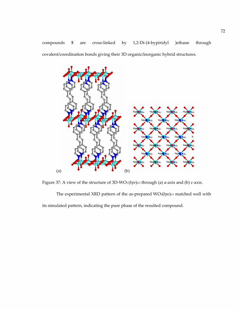
72
compounds 5 are cross-linked by 1,2-Di-(4-bypiridyl )ethane through
covalent/coordination bonds giving their 3D organic/inorganic hybrid structures.
(a) (b)
Figure 37: A view of the structure of 3D-WO3 (bpe)0.5 through (a) a-axis and (b) c-axis.
The experimental XRD pattern of the as-prepared WO3(bpe)0.5 matched well with
its simulated pattern, indicating the pure phase of the resulted compound.

73
Figure 38: Experimental (black) and simulated (red) XRD patterns of 3D-WO3(bpe)0.5.
3.1.2 2D-MO3(L)(L= organic ligand) structures
3.1.2.1 2D-MoO3(py) (py = pyridine)
Reactions of MoO3 (0.15g, 0.25 mmol) and pyridine (0.5ml) at 150 ˚C for 20 days
in thick-wall Pyrex tubes afforded yellow plate-like crystals of 2D-MoO3(py) (py =
pyridine) (6) (0.031g, 71.6% yield based on Se). The product was washed by ethanol,
water and anhydrous ethyl ether in sequence. (yield ca. 80% based on MoO3)
2D-MoO3(py) crystallizes in the space group Pbca, with the unit cell parameter of
a = 7.5228(4) Å, b = 7.3890(4) Å, c = 22.6080(13) Å. Similar to 3D-MoO3(4,4’-bpy), the
structure of 2D-MoO3(py) consists of layers of corner-sharing MoO5 square pyramids.
However, unlike the case of 3D-MoO3(4,4’-bpy), in which the layers of MoO5 square
10 20 30 40 50Two-Theta (deg)
0
5.0
10.0
15.0
20.0
25.0SQ
R(C
ount
s)
[WO3(bpe)0.5_Exp.mdi][Simu_WO3(bpe)0.5.raw]

74
pyramids are linked through 4,4’-bipyridyl groups into a three-dimensional framework,
the Mo atoms in 2D-MoO3(py) only bond with one nitrogen donor of pyridine ligands,
leading to a two dimemsional structure. The overall structure of 2D-MoO3(py) can be
described in terms of alternating MoO3(py) layers that are packed in a way ABAB.... The
long Mo-N distances, 2.395 Å on average, reflect the strong trans influence of the
terminal oxo group. The terminal Mo-O bond distances of 1.693 Å, on average, and the
bridging Mo-O bond distances, which range from 1.765 Å to 2.120 Å, strongly shows the
asymmetric effect as its parent structure.
(a) (b)
Figure 39: A view of the structure of 2D-MoO3(py) through (a) a-axis and (b) c-axis.
The experimental XRD pattern of the as-prepared 2D-MoO3(py) matched pretty
well with its simulated pattern, indicating the pure phase of the resulted compound.

75
Figure 40: Experimental (black) and simulated (red) XRD patterns of 2D-MoO3(py).
3.1.2.1 2D-WO3(py) (py = pyridine)
A stoichiometric mixture of Bi2O3 and WO3 was calcined at 800 C for 48 h to
synthesize Bi2W2O9. The products have been stirred in 1M hydrochloric acid for 5 days
to afford the pure H2W2O7·xH2O. The formed H2W2O7·xH2O (0.1 g) was then reacted
with pyridine (0.5ml) at 150 C for 10 days in thick-wall Pyrex tubes and give rise to
yellow powders of 2D-WO3(py) (py = pyridine) (7). The product was washed by ethanol,
water and anhydrous ethyl ether in sequence. (yield ca. 70% based on tungsten)
Powder X-ray diffraction (PXRD) of 2D-WO3(py) sample was performed on a
Rigaku D/M-2200T automated diffraction system (Ultima IV). The structural analyses
10 20 30 40 50Two-Theta (deg)
0
50
100
150
200
250
SQ
R(C
ount
s)
[MoO3(py)-10h_Exp.mdi][Simu_MoO3(py)(2D).raw]

76
were performed using JADE, PowderX and GSAS software packages. Due to the
similarity of XRD patterns between 2D-WO3(py) and 2D-MoO3(py), we assumed the
space group of 2D-WO3(py) is same as that of 2D-MoO3(py). And we also used other
structural information of 2D-MoO3(py) (e.g. lattice parameters and atomic positions) as
reference to build 2D-WO3(py) structural models for Rietveld refinement. The Rietvelt
refinement results are shown below. The experimental (black dots) and simulated (red
lines) XRD patterns matched pretty well, suggesting the proposed structure reflect real
crystal structure to a large extent. The structure of 2D-WO3(py) also crystallizes in
monoclinic lattice with the space group of Pbca, the lattice parameters of which are:
a=7.5024(0), b=7.4283(1), c=22.9359(2).
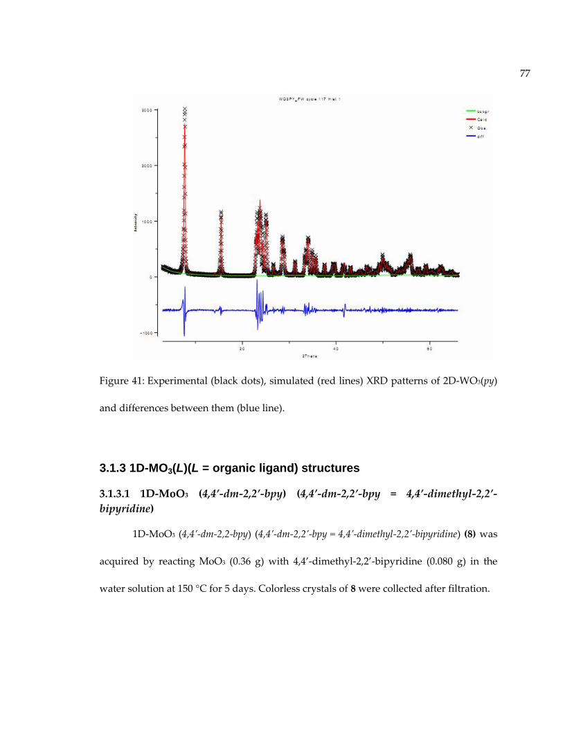
77
Figure 41: Experimental (black dots), simulated (red lines) XRD patterns of 2D-WO3(py)
and differences between them (blue line).
3.1.3 1D-MO3(L)(L = organic ligand) structures
3.1.3.1 1D-MoO3 (4,4’-dm-2,2’-bpy) (4,4’-dm-2,2’-bpy = 4,4’-dimethyl-2,2’-bipyridine)
1D-MoO3 (4,4’-dm-2,2-bpy) (4,4’-dm-2,2’-bpy = 4,4’-dimethyl-2,2’-bipyridine) (8) was
acquired by reacting MoO3 (0.36 g) with 4,4’-dimethyl-2,2’-bipyridine (0.080 g) in the
water solution at 150 °C for 5 days. Colorless crystals of 8 were collected after filtration.
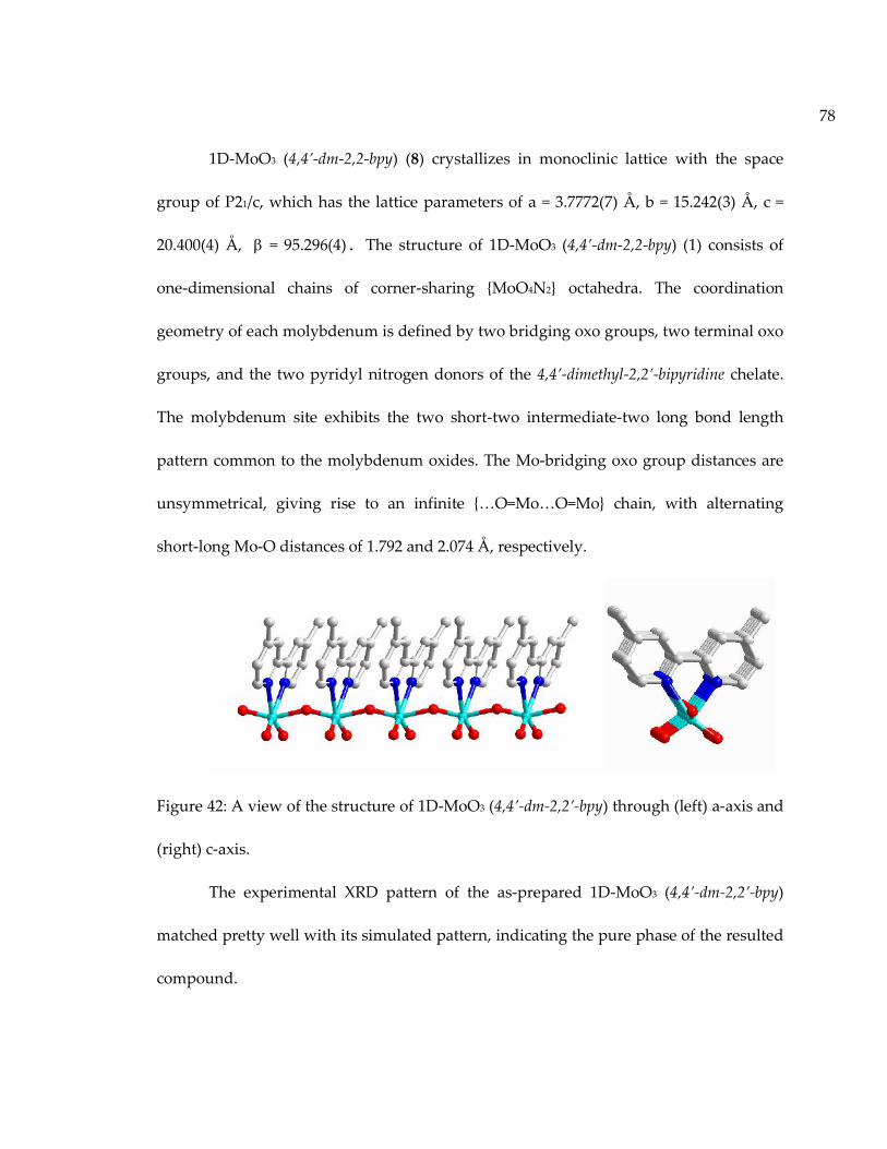
78
1D-MoO3 (4,4’-dm-2,2-bpy) (8) crystallizes in monoclinic lattice with the space
group of P21/c, which has the lattice parameters of a = 3.7772(7) Å, b = 15.242(3) Å, c =
20.400(4) Å, = 95.296(4). The structure of 1D-MoO3 (4,4’-dm-2,2-bpy) (1) consists of
one-dimensional chains of corner-sharing {MoO4N2} octahedra. The coordination
geometry of each molybdenum is defined by two bridging oxo groups, two terminal oxo
groups, and the two pyridyl nitrogen donors of the 4,4’-dimethyl-2,2’-bipyridine chelate.
The molybdenum site exhibits the two short-two intermediate-two long bond length
pattern common to the molybdenum oxides. The Mo-bridging oxo group distances are
unsymmetrical, giving rise to an infinite {…O=Mo…O=Mo} chain, with alternating
short-long Mo-O distances of 1.792 and 2.074 Å, respectively.
Figure 42: A view of the structure of 1D-MoO3 (4,4’-dm-2,2’-bpy) through (left) a-axis and
(right) c-axis.
The experimental XRD pattern of the as-prepared 1D-MoO3 (4,4’-dm-2,2’-bpy)
matched pretty well with its simulated pattern, indicating the pure phase of the resulted
compound.

79
Figure 43: Experimental (black) and simulated (red) XRD patterns of 1D-MoO3 (4,4’-dm-
2,2’-bpy).
3.1.3.2 1D-WO3 (4,4’-dm-2,2’-bpy) (4,4’-dm-2,2’-bpy = 4,4’-dimethyl-2,2’-bipyridine)
1D-WO3 (4,4’-dm-2,2’-bpy) (4,4’-dm-2,2’-bpy = 4,4’-dimethyl-2,2’-bipyridine) (9) was
acquired by reacting 3Na2WO4·9WO3·H2O (0.36 g) with 4,4’-dimethyl-2,2’-bipyridine
(0.080 g) in the water solution at 150 °C for 5 days. White powders of 9 were collected
after filtration.
Powder X-ray diffraction (PXRD) of 1D-WO3 (4,4’-dm-2,2’-bpy) sample was
performed on a Rigaku D/M-2200T automated diffraction system (Ultima IV). The
structure analyses were carried out using JADE (Windows), PowderX and GSAS
software packages. Due to the similarity of XRD patterns between 1D-WO3 (4,4’-dm-2,2’-
10 20 30 40 50Two-Theta (deg)
0
25
50
75S
QR
(Cou
nts)
[MoO3(44dm22bpy)_EXP.mdi][simu_MoO3(44dm22bpy).raw]
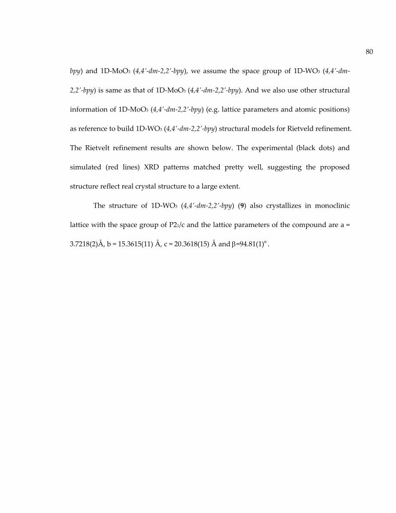
80
bpy) and 1D-MoO3 (4,4’-dm-2,2’-bpy), we assume the space group of 1D-WO3 (4,4’-dm-
2,2’-bpy) is same as that of 1D-MoO3 (4,4’-dm-2,2’-bpy). And we also use other structural
information of 1D-MoO3 (4,4’-dm-2,2’-bpy) (e.g. lattice parameters and atomic positions)
as reference to build 1D-WO3 (4,4’-dm-2,2’-bpy) structural models for Rietveld refinement.
The Rietvelt refinement results are shown below. The experimental (black dots) and
simulated (red lines) XRD patterns matched pretty well, suggesting the proposed
structure reflect real crystal structure to a large extent.
The structure of 1D-WO3 (4,4’-dm-2,2’-bpy) (9) also crystallizes in monoclinic
lattice with the space group of P21/c and the lattice parameters of the compound are a =
3.7218(2)Å, b = 15.3615(11) Å, c = 20.3618(15) Å and =94.81(1)º.
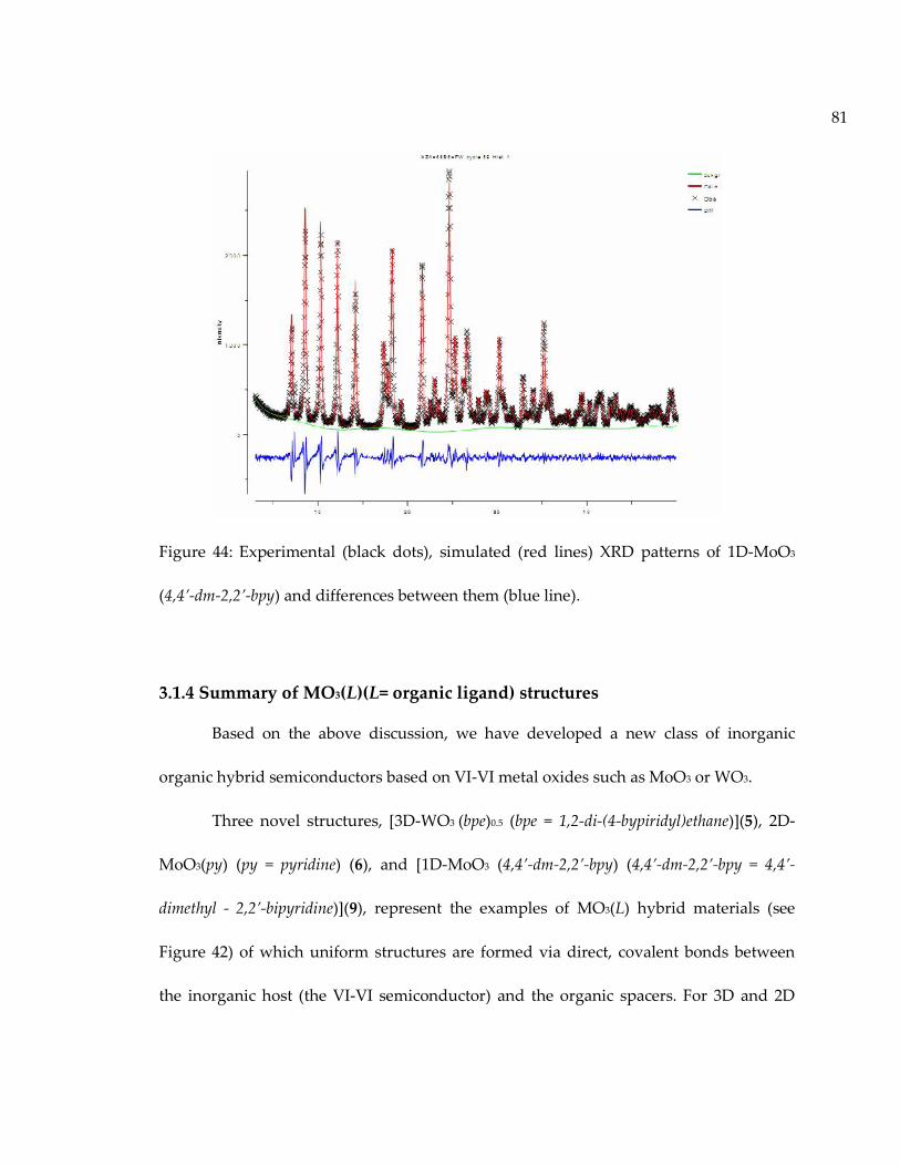
81
Figure 44: Experimental (black dots), simulated (red lines) XRD patterns of 1D-MoO3
(4,4’-dm-2,2’-bpy) and differences between them (blue line).
3.1.4 Summary of MO3(L)(L= organic ligand) structures
Based on the above discussion, we have developed a new class of inorganic
organic hybrid semiconductors based on VI-VI metal oxides such as MoO3 or WO3.
Three novel structures, [3D-WO3 (bpe)0.5 (bpe = 1,2-di-(4-bypiridyl)ethane)](5), 2D-
MoO3(py) (py = pyridine) (6), and [1D-MoO3 (4,4’-dm-2,2’-bpy) (4,4’-dm-2,2’-bpy = 4,4’-
dimethyl - 2,2’-bipyridine)](9), represent the examples of MO3(L) hybrid materials (see
Figure 42) of which uniform structures are formed via direct, covalent bonds between
the inorganic host (the VI-VI semiconductor) and the organic spacers. For 3D and 2D

82
hybrid structures, they consist of inorganic layers of corner-sharing {WO5N} or
octahedra linked with organic molecules to form 3D or 2D framework. This can be
described as a single “slice” which is cut from the parent structure and one oxygen in
MO6 octahedra of WO3 or MoO3 perovskite phase is substituted by the nitrogen atom in
the pyridine ring of organic molecules. While for 1D structure, each tungsten atom is
octahedrally coordinated to four oxygen atoms and two nitrogen atoms from a chelating
4,4’-dimethyl-2,2’-bipyridine molecule. {WO4N2} octahedra are interconnected with
oxygen atom, forming an infinite WO2N chain. This can be described as a single “chain”
cut from the parent WO3 perovskite phase with two oxygen in WO6 octahedra
substituted by the two nitrogen atoms in the 4,4’-dimethyl-2,2’-bipyridine.
(a) (b)

83
(c) (d)
Figure 45: Crystal structures of (a) 3D-WO3(bpe)0.5 (5), (b) 2D-MoO3(py) (6), (c) 1D-WO3
(4,4’-dm-2,2’-bpy) (9), (d) MoO3 or WO3 perovskite structures.
The structural information of all the listed compounds including their unit cell
parameters and space groups are shown below.
Table 9: List of compounds107-109 with their unit cell parameters, space groups, and band
gaps.
Compounds Unit cell Parameters (Å) SGa
3D-MoO3 (pyz)0.5 (1) a=5.2702(15) b=5.2674(7) c=14.2310(11) I222
3D-WO3 (pyz)0.5 (2) a=5.2288(7) b=5.2288(7) c=14.175(3) I4/mmm
3D-MoO3(4,4’-bpy)0.5 (3) a= 7.5727(6) b=7.3675(7) c= 22.433(3)
=90.396(8)
P21/c
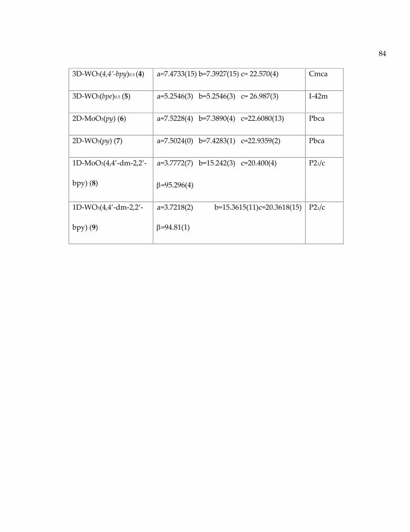
84
3D-WO3(4,4’-bpy)0.5 (4) a=7.4733(15) b=7.3927(15) c= 22.570(4) Cmca
3D-WO3(bpe)0.5 (5) a=5.2546(3) b=5.2546(3) c= 26.987(3) I-42m
2D-MoO3(py) (6) a=7.5228(4) b=7.3890(4) c=22.6080(13) Pbca
2D-WO3(py) (7) a=7.5024(0) b=7.4283(1) c=22.9359(2) Pbca
1D-MoO3(4,4’-dm-2,2’-
bpy) (8)
a=3.7772(7) b=15.242(3) c=20.400(4)
=95.296(4)
P21/c
1D-WO3(4,4’-dm-2,2’-
bpy) (9)
a=3.7218(2) b=15.3615(11)c=20.3618(15)
=94.81(1)
P21/c

85
3.2 Optical absorption properties of MO3(L)
The optical absorption spectra of 3D-MoO3 (pyz)0.5 (1), 3D-MoO3(4,4’-bpy)0.5 (3),
2D-MoO3(py) (6) and 1D-MoO3(4,4’-dm-2,2’-bpy) (8) and MoO3 parent structure were
measured by diffuse reflectance experiments at room temperature with a Shimadzu UV-
3101PC double beam, double monochromator spectrophotometer. Data were collected in
the wavelength range of 300-800 nm and converted using the Kubelka-Munk function..
BaSO4 powder was used as a standard (100% reflectance). The scattering coefficient (S)
was treated as a constant since the average particle size of the samples used in the
measurements was greatly larger than 5 nm, and the results are plotted in Figure 46,
along with that of perovskite MoO3. The absorption edges for 1, 3 and 6 are found to be
of 2.2, 2.3, and 2.4 eV, respectively. Compared to the measured value of 2.9 eV for
perovskite type MoO3, it clearly indicates a very significant red shift (0.7, 0.6 and 0.5 eV,
respectively).
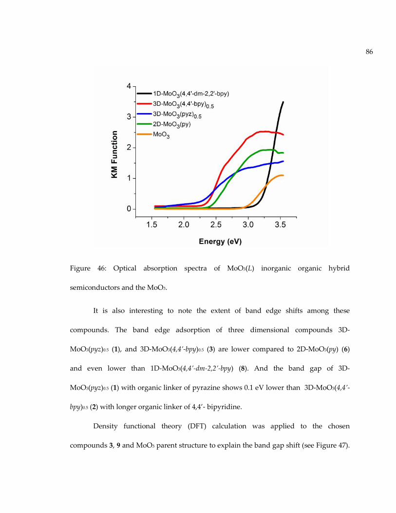
86
Figure 46: Optical absorption spectra of MoO3(L) inorganic organic hybrid
semiconductors and the MoO3.
It is also interesting to note the extent of band edge shifts among these
compounds. The band edge adsorption of three dimensional compounds 3D-
MoO3(pyz)0.5 (1), and 3D-MoO3(4,4’-bpy)0.5 (3) are lower compared to 2D-MoO3(py) (6)
and even lower than 1D-MoO3(4,4’-dm-2,2’-bpy) (8). And the band gap of 3D-
MoO3(pyz)0.5 (1) with organic linker of pyrazine shows 0.1 eV lower than 3D-MoO3(4,4’-
bpy)0.5 (2) with longer organic linker of 4,4’- bipyridine.
Density functional theory (DFT) calculation was applied to the chosen
compounds 3, 9 and MoO3 parent structure to explain the band gap shift (see Figure 47).

87
Compared to 0.53 eV, the band gap of MoO3, 3 and 9 show larger values of 1.685 eV and
2.715 eV respectively. This trend is corresponding to what we observed in II-VI hybrid
materials, when the dimension of inorganic structures is reduced from 3D to 1D, strong
quantum confinement effect results in larger fundamental band gap6,110,111. In addition,
the calculation results reveal the indirect band gap of MoO3 but direct band gap of both
3 and 9, the latter one is always desired for semiconductors with different kind of
applications.
Figure 47: Band structure of 3D-MoO3(4,4’-bpy)0.5 with direct band gap of 1.685 eV.

88
Figure 48: Band structure of 1D-MoO3 (4,4’-dm-2,2’-bpy) with direct band gap of
2.715eV.
Figure 49: Band structure of MoO3 with indirect band gap of 0.513eV.

89
The atomic contribution to valence band and conduction band can be studied by
looking into the density of state results plotted in both inorganic part and organic part of
3D-MoO3(4,4’-bpy)0.5 and 1D-MoO3 (4,4’-dm-2,2’-bpy) hybrid structures.
Figure 49 reveals that the 2p-obitals of oxygen atoms in 3D-MoO3(4,4’-bpy)0.5
inorganic layer contribute significantly more to the valence band, compared to 2p-obitals
of nitrogen atoms and 2p-obitals of carbon atoms, which also contribute a lot to the
valence band. While to the conduction band, the contribution is made by different
orbitals such as 4d orbitals of molybdenum atoms, 2p-obitals of oxygen atoms, 2p-
obitals of carbon atoms, and 2p-obitals of nitrogen atoms, respectively. When adding up
the contribution from different atoms, we found that the atomic orbitals in MoO5N
octahedra dominate the conduction band and valence band.
Figure 50: Density of states of inorganic part (left) and organic part (right) of 3D-
MoO3(4,4’-bpy)0.5.
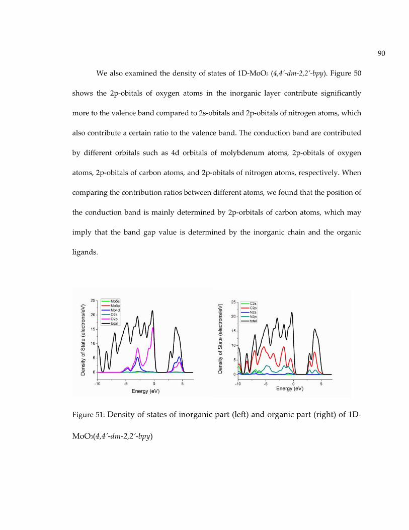
90
We also examined the density of states of 1D-MoO3 (4,4’-dm-2,2’-bpy). Figure 50
shows the 2p-obitals of oxygen atoms in the inorganic layer contribute significantly
more to the valence band compared to 2s-obitals and 2p-obitals of nitrogen atoms, which
also contribute a certain ratio to the valence band. The conduction band are contributed
by different orbitals such as 4d orbitals of molybdenum atoms, 2p-obitals of oxygen
atoms, 2p-obitals of carbon atoms, and 2p-obitals of nitrogen atoms, respectively. When
comparing the contribution ratios between different atoms, we found that the position of
the conduction band is mainly determined by 2p-orbitals of carbon atoms, which may
imply that the band gap value is determined by the inorganic chain and the organic
ligands.
Figure 51: Density of states of inorganic part (left) and organic part (right) of 1D-
MoO3(4,4’-dm-2,2’-bpy)

91
Interesting optical absorption results are also found in WO3(L) organic- inorganic
hybrid materials and shown in Figure 52. Compared to 2.6 eV of the band gap of WO3,
compounds 2, 4, 5, 7 and 9 display band gap absorption in lower energy area from 2.2
eV of 3D-WO3(pyz)0.5, 2.25 eV of 3D-WO3(4,4’-bpy)0.5 to 2.3 eV of 3D-WO3 (bpe)0.5, which
are 0.4 eV, 0.35eV and 0.3 eV less than 2.6 eV of WO3 band gap. As the length of organic
linkers increases, the band absorption edges of the three dimensional WO3(L)
compounds slightly shifts to a higher energy. 2D-WO3(py) show absorption edge around
2.2 eV, yet the intensity is not as strong as its 3D and 1D brothers. 1D-WO3(2,2’-bpy),
which starts to absorb light above 3.2 eV, not only displays a large blue shift of 0.6 eV,
but also shows strong optical absorption ability as well.
Figure 52: Optical absorption spectra of WO3(L) inorganic organic hybrid
semiconductors and their parent WO3.

92
3.3 Thermal stability of MO3(L)
The thermogravimetric (TG) analyses of polycrystalline samples of both MoO3(L) and
WO3(L) inorganic organic hybrid structures were performed on a computer-controlled
TA Instrument TG Q50 analyzer. Single-phased powder samples were loaded into
platinum pans and heated with a ramp rate of 5 °C/min from room temperature to 600
°C, and the results are summarized in Table 10. Figure 53 shows the good thermal
stabilities for all the compounds and also single-step weight losses observed for 3D-
MoO3(pyz)0.5 (1), 3D-MoO3(4,4’-bpy)0.5 (3), 2D-MoO3(py) (6), 1D-MoO3(2,2’-dm-4,4’-bpy) (8).
As shown in the TG curves, all four compounds exhibit good thermal stability. The three
dimensional compounds 3D-MoO3(pyz)0.5 (1) and 3D-MoO3(4,4’-bpy)0.5 (3) are most
thermally stable since the decomposition of organic ligands in both materials start after
300°C, which is higher than 250 °C for 2D-MoO3(py) (6) and 160°C for 1D-MoO3(2,2’-bpy)
(8) respectively. The measured weight losses of the organic species are 22% for pyrazine
in 1, 35% for 4,4’-bipyridine in 3, 32% for pyridine in 6 and 52% for 2,2’-bipyridine in 8,
in reasonable agreement with the calculated values of 22% for pyrazine, 35% for 4,4’-
bipyridine, 32% for pyridine, and 53% for 2,2’-bipyridine, respectively. Powder X-ray
diffraction patterns shows the residues of all samples are nanoparticles of MoO3
perovskite structures.

93
Figure 53: TGA profile of (a) MoO3(L) inorganic organic hybrid materials.
Table 10: The calculated and experimental TGA weight loss of MoO3 based inorganic
organic hybrid structures.
Compound WL %
(calcd)
WL %
(exptl)
Td (°C) Residue
3D-MoO3(pyz)0.5 (1) 22 22 300 MoO3 (p)
3D-MoO3(4,4’-bpy)0.5 (3) 35 35 310 MoO3(p)
2D-MoO3(py) (6) 35 32 160 MoO3(p)
1D-MoO3(4,4’-dm-2,2’-bpy) (8) 52 53 270 MoO3(p)
Td: Temperature of decomposition.

94
Similar behavior was also observed in WO3(L) inorganic organic hybrid
semiconductors, for compounds underwent one-step weight losses from room
temperature to 650 °C (see Figure 54). As what we observed in MoO3(L) hybrid materials,
WO3(L) also showed the thermal stability are dependent on the structures with a trend
of three dimensional structures > one dimensional structures > two dimensional
structures. To be specific, 3D structures 3D-WO3(pyz)0.5 (2), 3D-WO3(4,4’-bpy)0.5 (4) and
3D-WO3 (bpe)0.5 (5) showed the best thermal stability with onset temperature of 400°C.
Particularly, WO3(pyz)0.5 did not decompose 520 °C as stable as many inorganic materials.
1D-WO3(2,2’-bpy) and 2D-WO3(py) were less thermally stable and decomposed at 320°C
and 180°C, respectively. The TG weight loss for each compound matched with the mass
ratio of its organic ligand. The experimental weight losses of the organic species are 15%
for pyrazine in 2, 24% for 4,4’-bipyridine in 4, 27% for 1,2-Di-(4-bypiridyl )ethane in 5,
24% for pyridine in 7 and 40% for 2,2’-bipyridine in 9, respectively, in reasonable
agreement with the calculated values of 14% for pyrazine, 25% for 4,4’-bipyridine, 28%
for 1,2-Di-(4-bypiridyl)ethane, 20% for pyridine, and 41% for 2,2’-bipyridine respectively.
The post-TGA residuals were found to be perovskite WO3. Based on the TG results of
both MoO3(L) and WO3(L) inorganic organic hybrid structures, we can confirm that all
the reported reaction conditions can give pure phase hybrid materials with good
thermal stability. The high thermal stability allow the MoO3(L) and WO3(L) hybrid
structures to be annealed to make pallets and films for future research and application.

95
Figure 54: TGA profile of WO3(L) inorganic organic hybrid materials.
Table 11: The calculated and experimental TGA weight loss of WO3 based inorganic
organic hybrid structures.
Compound WL %
(calcd)
WL %
(exptl)
Td (°C) Residue
3D-WO3(pyz)0.5 (2) 15 14 520 WO3(p)
WO3(4,4’-bpy)0.5 (4) 24 25 400 WO3(p)
3D-WO3(bpe)0.5·0.14 H2O (5) 27 28 400 WO3(p)
2D-WO3(py) (7) 24 20 180 WO3(p)
1D-WO3(4,4’-dm-2,2’-bpy) (9) 40 41 320 WO3(p)
Td: Temperature of decomposition.
96
3.4 Dielectric properties of MO3(L)
One of the advantages of inorganic organic hybrid semiconductors is to
introduce a number of interfaces between adjacent layers and the interfaces sometimes
lead to unique properties. To explore the interface between inorganic and organic layers,
we were trying to measure free dielectric constant and dielectric loss on selected
inorganic organic hybrid materials. The as synthesized MoO3(4,4’-bpy)0.5, MoO3(py),
MoO3 samples were grinded into fine powders and then compressed into pallets and
further annealed at 275 ºC, 175 ºC and 600 ºC for dielectric measurements. The pallets
were covered with silver paint and dried at room temperature. The free dielectric
constant and dielectric loss were measured at 1 kHz by an impedance analyzer HP4194A.
The results are shown in Figure 55. In the frequency range from 10KHz to 1MHz, both
the MoO3(4,4’-bpy)0.5 and MoO3(py) show higher dielectric constants than their parent
structure MoO3. Hybrid structures start with very high dielectric constants (1400 for
MoO3(4,4’-bpy)0.5 and 350 for MoO3(py)) and decrease dramatically before 100KHz, which
is the evidence of space charge polarization in the hybrid structures, since the space
charges vibrate most strongly when applied with low frequency alternating current (AC)
electric field.112 The space charge assumption is further proved by comparing their
dielectric losses in Figure 55. At low frequency range, hybrid structures show higher
dielectric loss and is negatively correlated with frequency, which is as result of the
charge leakage when plenty of space charges accumulate on the structural boundaries.
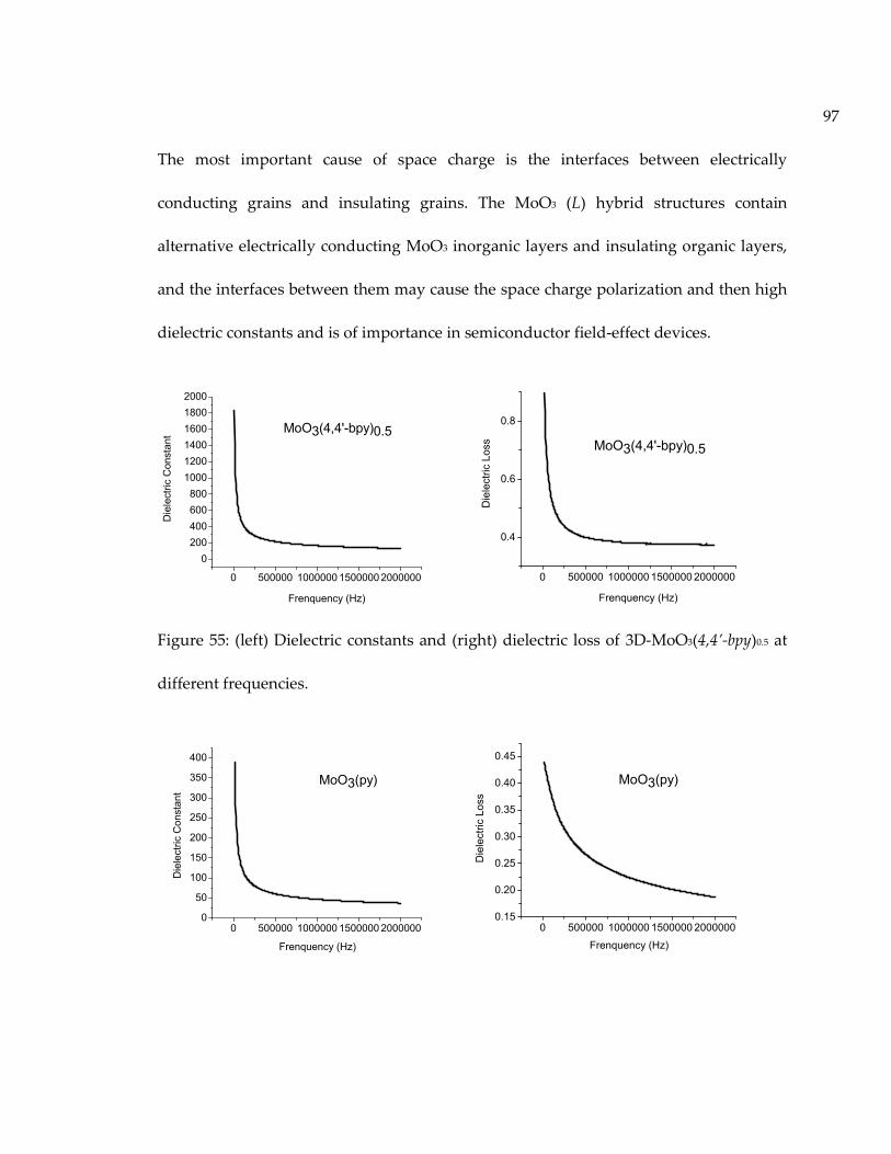
97
The most important cause of space charge is the interfaces between electrically
conducting grains and insulating grains. The MoO3 (L) hybrid structures contain
alternative electrically conducting MoO3 inorganic layers and insulating organic layers,
and the interfaces between them may cause the space charge polarization and then high
dielectric constants and is of importance in semiconductor field-effect devices.
0 500000 1000000 1500000 2000000
0200400600800
100012001400160018002000
Die
lect
ric C
onst
ant
Frenquency (Hz)
MoO3(4,4'-bpy)0.5
0 500000 1000000 1500000 2000000
0.4
0.6
0.8
MoO3(4,4'-bpy)0.5
Frenquency (Hz)
Die
lect
ric L
oss
Figure 55: (left) Dielectric constants and (right) dielectric loss of 3D-MoO3(4,4’-bpy)0.5 at
different frequencies.
0 500000 1000000 1500000 20000000
50
100
150
200
250
300
350
400
Frenquency (Hz)
Die
lect
ric C
onst
ant
MoO3(py)
0 500000 1000000 1500000 20000000.15
0.20
0.25
0.30
0.35
0.40
0.45
MoO3(py)
Die
lect
ric L
oss
Frenquency (Hz)
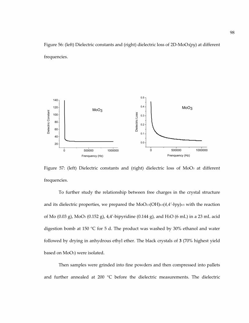
98
Figure 56: (left) Dielectric constants and (right) dielectric loss of 2D-MoO3(py) at different
frequencies.
0 500000 1000000
20
40
60
80
100
120
140
Die
lect
ric C
onst
ant
Frenquency (Hz)
MoO3
0 500000 1000000
0.0
0.1
0.2
0.3
0.4
0.5
MoO3
Frenquency (Hz)
Die
lect
ric L
oss
Figure 57: (left) Dielectric constants and (right) dielectric loss of MoO3 at different
frequencies.
To further study the relationship between free charges in the crystal structure
and its dielectric properties, we prepared the MoO2.5(OH)0.5(4,4’-bpy)0.5 with the reaction
of Mo (0.03 g), MoO3 (0.152 g), 4,4’-bipyridine (0.144 g), and H2O (6 mL) in a 23 mL acid
digestion bomb at 150 °C for 5 d. The product was washed by 30% ethanol and water
followed by drying in anhydrous ethyl ether. The black crystals of 3 (70% highest yield
based on MoO3) were isolated.
Then samples were grinded into fine powders and then compressed into pallets
and further annealed at 200 °C before the dielectric measurements. The dielectric

99
measurements were carried out in the same condition as of MoO3(4,4’-bpy)0.5 and the
results show that the dielectric constants of MoO2.5(OH)0.5(4,4’-bpy)0.5 can be as high as
1000, almost ten times higher than its similar structure, MoO3(4,4’-bpy)0.5. This difference
is mainly caused by the free charge in MoO2.5(OH)0.5(4,4’-bpy)0.5. The valence state of Mo
is +5, with one electron in its d-orbital, while the Mo in MoO3(4,4’-bpy)0.5 is +6, with no
electron staying in its d-orbital. The free charges in the crystal structure will largely flow
under the external electric field until the later one is balanced by the self-generated
internal electric field to obtain electrostatic equilibrium, which causes the extremely high
dielectric constant. This can be further confirmed by the high dielectric loss of
MoO2.5(OH)0.5(4,4’-bpy)0.5 compound. The free-moving electrons will accumulate on the
sample surface and cause the leakage under the external electric field, leading to the
high dielectric loss as shown in the Figure 58.
0 500000 1000000 1500000 20000000
2000
4000
6000
8000
10000
MoO2.5(OH)0.5(4,4'-bpy)0.5
Frenquency (Hz)
Die
lect
ric C
onst
ant
0 500000 1000000 1500000 2000000
0
5
10
15
20
25
Die
lect
ric lo
ss
Frequency (Hz)
MoO2.5(OH)0.5(4,4'-bpy)0.5
Figure 58: (left) Dielectric constants and (right) dielectric loss of MoO2.5(OH)0.5(4,4’-bpy)0.5
at different frequencies.

100
3.5 Thermoelectric properties of MO3(L)
The thermal conductivity (TC) of selected MoO3(4,4’-bpy)0.5 and WO3(4,4’-bpy)0.5
samples on behalf of MoO3(L) and WO3(L) series were determined by the density,
specific heat capacity, and thermal diffusivity.
The thermal conductivity can be calculated by the following equation: k(T) =
a(T) · Cp(T) · d(T)
k is the thermal conductivity of the sample, in [W·m−1·K−1],
a is the thermal diffusivity of the sample, in [m2 ·s−1],
Cp is the specific heat of the sample, in [J·kg−1·K−1]
d is the density of the sample, in [kg·m−3].
The results of the thermal conductivity measurements are shown in Figure 59.
Both the MoO3(4,4’-bpy)0.5 and WO3(4,4’-bpy)0.5 samples have thermal conductivity ~ 0.3
W*m/K at 101°C, about 80% less than ~1.5 W*m/K for both MoO3 and WO3 samples
prepared by cold-pressing process. Over a temperature range from 25°C to 101°C, the
thermal conductivity of MoO3 and WO3 decrease all the way as the temperature increase.
Unlike the trend observed in inorganic oxides, MoO3(4,4’-bpy)0.5 and WO3(4,4’-bpy)0.5
keep the TC almost unchanged. The thermal conductivity of MoO3(4,4’-bpy)0.5 is a little
higher than WO3(4,4’-bpy)0.5, which is similar to their parent structure, for the TC of
MoO3 is also a little higher than WO3.

101
Figure 59: Thermal conductivities of compounds MoO3 (■), WO3 (●), MoO3(4,4’-bpy)0.5
(▲) and WO3(4,4’-bpy)0.5 (▼).
The cause of low thermal conductivity of hybrid structures can be understood by
a closer look at the three parameters that determine thermal conductivity. Thermal
diffusivity of the selected hybrid materials and their parent structures are plotted in
Figure 60. When the inorganic layers are separately by organic molecules, the resulted
interfaces at atomic scale can increase phonon scattering. As the phonon scattering
enhanced, a large amount of the heat (phonons) dissipate during the movement and
cause thermal diffusivity to be reduced. This mechanism results in the difference as
shown in Figure 60. Over a temperature range from 25 °C to 101 °C, the thermal
diffusivity of MoO3(4,4’-bpy)0.5 and WO3(4,4’-bpy)0.5 stays lower than one fourth

102
compared to their parent structures, mainly contributing to the low thermal
conductivity of hybrid materials.
Figure 60: thermal diffusivities of compounds MoO3 (■), WO3 (●), MoO3(4,4’-
bpy)0.5 (▲), WO3(4,4’-bpy)0.5 (▼).
Heat capacity (HC) of the selected MO3(L) structures is slightly higher than their
parent structure, for the HC of MoO3(4,4’-bpy)0.5 (~ 0.75 J·kg−1·K−1) and WO3(4,4’-bpy)0.5 (~
0.60 J·kg−1·K−1) are about 1.3 and 1.8 times of the HC of WO3 (0.53 J·kg−1·K−1) and MoO3
(0.33 J·kg−1·K−1). In all four compounds, the heat capacity is positively correlated with the
temperature. The increase in heat capacity is offset by the lower density of inorganic
organic hybrid structures.

103
Figure 61: Heat capacities of compounds MoO3 (black), WO3 (red), MoO3(4,4’-bpy)0.5
(blue) and WO3(4,4’-bpy)0.5 (purple).
The density of the pallet-form samples are measured by dividing the masses by
the volumes and the results are comparable with the unit cell density presented in Table
12. All four cases show that the experimental densities are lower than unit cell densities
due to the space between packing particles, but the trend of experimental density data,
(4.79 g/cm3 for WO3 > 3.15 g/cm3 for MoO3 > 2.61 g/cm3 for WO3(4,4’-bpy)0.5 > 1.94 g/cm3)
for MoO3(4,4’-bpy)0.5 is consistent to the trend of unit cell density data (7.16 g/cm3 for
WO3 > 4.69 g/cm3 for MoO3 > 3.30 g/cm3 for WO3(4,4’-bpy)0.5 > 2.26 g/cm3 for MoO3(4,4’-
bpy)0.5) and the experimental densities of MoO3(4,4’-bpy)0.5 and WO3(4,4’-bpy)0.5 show

104
~30% and ~40% less than the densities of inorganic oxides which is another reason for
low thermal conductivity of the hybrid materials.
Table 12: The experimental density and unit cell density of selected MO3(L) hybrid
structures and their parent structures.
In summary, the apparent decreases in thermal conductivity and density,
together with a tender increase in heat capacity result in the low thermal conductivity of
MoO3(4,4’-bpy)0.5 and WO3(4,4’-bpy)0.5 inorganic organic hybrid materials with almost one
order less TC coefficient than their parent MoO3 and WO3 structure.
Compounds Experimental
density g/cm3
Calculated
density g/cm3
MoO3 3.15 4.69
WO3 4.79 7.16
MoO3(4,4-bpy)0.5 1.94 2.36
WO3(4,4-bpy)0.5 2.61 3.30

105
3.6 Thermal expansion properties of MO3(L)
3.6.1 MoO3(4,4’-bpy)0.5
Negative thermal expansion (NTE) and nearly zero thermal expansion (ZTE)
behaviors were found in our II-VI inorganic organic hybrid structures as discussed in
chapter 1. To explore whether the VI-VI hybrid system also show similar thermal
expansion behavior, we collected X-ray diffraction patterns of MoO3(4,4’-bpy)0.5 at a
number of temperatures between 28 °C and 265 °C.
The unit cell parameters of MoO3(4,4’-bpy)0.5 at each temperature was well
defined based on Pawley refinement. Figure 62 shows the simulated MoO3(4,4’-bpy)0.5
pattern at 28 °C matched pretty well with the experimental data, and the Goof value and
Rwp vale are ~ 1.45 and 0.0146 respectively, indicating the good refinement results and
reliability of the refined unit cell parameters.
2 Theta (deg) Cu60555045403530252015105
Inte
nsity
(a.u
.)
50,000
45,000
40,000
35,000
30,000
25,000
20,000
15,000
10,000
5,000
0
hkl_Phase 0.00 %

106
Figure 62: The experimental and simulated MoO3(4,4’-bpy)0.5 patterns at 28°C, and the
differences between two patterns.
The temperature dependent lattice parameters a, b, c and are plotted in Figure
63. According to the results, the b-axis shows very interesting negative thermal
expansion behavior in the whole temperature range and the thermal expansion (TE)
coefficient can be as large as -1.5 ×10⁻⁵ K-1, among the largest NTE values reported to date.
Figure 63: Temperature dependent lattice parameters of MoO3(4,4’-bpy)0.5 in a-axis and b-
axis.

107
Figure 64: Temperature dependent lattice parameters of MoO3(4,4’-bpy)0.5 in a-axis and -
angle.
Figure 65: Temperature dependent volume of MoO3(4,4’-bpy)0.5.

108
Unlike the NTE behavior observed in the c-axis (long axis) in II-VI hybrid
structures where the inorganic layers and organic layers packed, the b-axis (short axis)
show NTE in MoO3(4,4’-bpy)0.5 structure. This is interesting because similar anisotropic
NTE behavior was also observed in the b-axis of 2D-MoO3 layered structure, and the
later one has -0.3×10⁻⁵ K-1 of its TE coefficient. By comparing the structures between
inorganic layer of MoO3(4,4’-bpy)0.5 and the layer of -MoO3 structure, we found many
similarities between their bond distances, angles and symmetries. (see Figure 66). These
similarities may help to explain their similar negative thermal expansion behavior due
to the possibly similar phase transition or thermal motion of atoms.

109
Figure 66: Structural comparison between 2D-MoO3 (left) and MoO3(4,4’-
bpy)0.5(right).
3.6.2 WO3(4,4’-bpy)0.5
Negative thermal expansion (NTE) behavior was also found in WO3(4,4’-bpy)0.5.
We collected x-ray diffraction patterns of WO3(4,4’-bpy)0.5 at a number of temperatures
between -200 °C and 225 °C. The unit cell parameters of WO3(4,4’-bpy)0.5 at different
temperatures were also determined by Pawley refinement. The temperature dependent
lattice parameters a, b, c and V are plotted in Figure 67. According to the results, the a-
axis (short axis) shows interesting negative thermal expansion behavior in the
temperature range between -150 °C and 225 °C and the thermal expansion (TE)
coefficient can be as large as -1.7 ×10⁻⁵ K-1.
-200 -100 0 100 200 300
7.48
7.49
7.50
7.51
7.52
7.53
Temperature (oC)
a (A
)
-200 -100 0 100 200 3007.39
7.40
7.41
7.42
7.43
7.44
7.45
Temperature (oC)
b (A
)
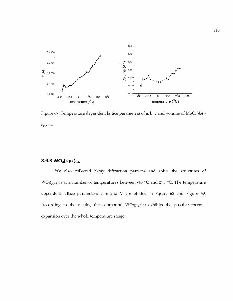
110
-200 -100 0 100 200 30022.55
22.60
22.65
22.70
22.75
c (A
)
Temperature (oC)
-200 -100 0 100 200 3001250
1255
1260
1265
1270
1275
1280
Vol
ume
(A3 )
Temperature (oC)
Figure 67: Temperature dependent lattice parameters of a, b, c and volume of MoO3(4,4’-
bpy)0.5.
3.6.3 WO3(pyz)0.5
We also collected X-ray diffraction patterns and solve the structures of
WO3(pyz)0.5 at a number of temperatures between -43 °C and 275 °C. The temperature
dependent lattice parameters a, c and V are plotted in Figure 68 and Figure 69.
According to the results, the compound WO3(pyz)0.5 exhibits the positive thermal
expansion over the whole temperature range.

111
Figure 68: Temperature dependent lattice parameters of a, c and volume of WO3(pyz)0.5.
Figure 69: Temperature dependent volume of WO3(pyz)0.5.

112
A closer look at details of the powder x-ray diffraction shows the interesting
phase transition between -175 °C to -30 °C. As shown in the Figure 70 and Figure 71. As
the temperature decreases from -30 °C to -175 °C, both the single peaks at 23.8°
corresponding to (110) plane and the single peak at 26.9° corresponding to (112) plane
are separated into two peaks. This phenomenon is probably caused by the structural
change from higher symmetry to lower symmetry since the later one is always preferred
in low temperature.
Figure 70: Background subtracted XRD patterns of WO3(pyz)0.5 from -30 °C to -175 °C.

113
Figure 71: Background subtracted XRD patterns of WO3(pyz)0.5 from -30 °C to -175 °C for
two theta values between 22° and 29°.
3.7 Summary
In summary, we have designed a new class of inorganic organic hybrid
semiconductors with one-dimensional, two-dimensional and three-dimensional
periodically ordered nanostructures with chainlike and layered inorganic VI-VI
structural motifs under mild solvothermal conditions. By controlling the dimensionality
and topology of the VI-VI inorganic component using organic spacers, hybrid
semiconductors with tunable optical properties can be effectively designed and
fabricated to meet the specific needs in device applications. Benefited from the good
114
thermal stability of new hybrid structures, we are able to study a series of physical
properties such as thermoelectric, dielectric and thermal expansion properties which
require high-temperature sample treatment. In these property studies, our VI-VI hybrid
structures display desired and significantly low thermal conductivities and high
dielectric constants caused by interface induced phonon scattering and space charge
polarization respectively, while negative thermal expansions is related to the similar
structural features between inorganic layer of MoO3(4,4’-bpy)0.5 and the 2D-MoO3 layered
structure. The interesting properties generated by the unique inorganic organic hybrid
structures open a new and promising approach to multifunctional materials in advanced
technology.

115
4. I-VII inorganic organic hybrid semiconductors
Concerns about global warming have led to a worldwide effort in the science
community to reduce greenhouse gas emissions and to increase energy efficiency.
Conservation of energy through gradual diversion of resources to renewable green
energy paves the way for tomorrow’s consumption and a cleaner environment. Solid-
state lighting (SSL) technology in the form of light-emitting diodes (LEDs) generates
high-efficient light sources, converts electricity into light up to 25% more effectively than
conventional lighting sources.113 The U.S. Department of Energy has estimated that
switching to LED lighting over the next two decades could save the country $250 billion
in energy costs over that period; this reduces the electricity consumption for lighting by
nearly one half, and avoid 1,800 million metric tons of carbon emission. Low-cost and
high-efficiency white light-emitting diodes or WLEDs (144 lm/W) are considered a
potential light source to replace conventional incandescent (15 lm/W) or fluorescent
lighting (114 lm/W) prevalent in major infrastructures.12 Other applications in everyday
lives range from computer displays to car headlights. However, major setbacks of SSL
are the cost of using RE (rare-earth) elements and its lack of recyclability, which is
destructive to the environment. Today, the purchase price of WLED lighting products is
significantly higher than that of their conventional counterparts, and the energy savings
often are not enough to offset the difference within an attractive payback period.
Common approaches to produce WLEDs include blending of three primary colored
116
LEDs, namely red, green, and blue (RGB) diodes, or combination of a blue (or UV) LED
with a yellow phosphor (or multiphosphors). Either process requires complex
doping/mixing and delicate control of multiple materials and colors, which proves both
challenging and costly.114-117 At the present time, commercially available WLEDs are
predominantly phosphor based (e.g. a yellow-emitting phosphor, yttrium aluminum
garnet or (YAG):Ce3+, coupled with a blue-emitting InGaN/GaN diode).118 While less
expensive than the RGB diodes, the (YAG):Ce3+ type phosphors and WLEDs have issues
such as unsuitability for solution process, poor color rendering index (CRI), high
correlated color temperature (CCT) and dependence on rare earth component which
then limits their widespread commercialization in general lighting market. Developing
new white phosphors that are energy efficient while also cost effective and, REs free, is
of great interest worldwide.117,119
A good candidate for white phosphors of this type is CuI based hybrid materials.
These materials are built on environmentally friendly CuI which has sharp emission
between 400 nm to 450 nm and organic ligands such as 2,6-dimethylpyrazine, which can
emits at in the UV range. When integrating the inorganic modules and organic ligands
into the single crystal structure with coordination bond between the copper ions and
nitrogen atoms, interesting yellow fluorescence is obtained, very different from both of
its components. Our preliminary studies show that the emission of CuI(2,6
dimethylpyrazine) is primarily a band gap emission, namely, electrons are first excited

117
to the conduction band upon irradiation, then relaxed to the valence band, giving the
emission in the visible light region. A closer look at the DFT calculation results reveals
that the valence band of the compound mainly consists of the 3d orbitals of copper and
the 5p orbitals of iodide, while the conduction band is mainly made of the 2p orbitals of
carbon and nitrogen atoms. This result suggests the band gap emission involves a
charge transfer from the organic molecules to the CuI inorganic orbitals. Based on this
observation, by changing the functional group (electron donating or electron
withdrawing group) on the organic molecules, the LUMO energy of the organic
molecules, and thereby the conduction band of the hybrid structures, can be
systematically tuned. The strong tunability of the band structure may lead to white light
emission. The application of copper iodide complexes in OLEDs has recently been
demonstrated that codeposition of CuI and 3,5-bis(carbazol-9-yl)pyridine (mCPy) is an
efficient way to utilize CuI complexes as emissive materials in OLEDs.120 Devices made
using CuI:mCPy films shows pure green electroluminescence (EL) from a Cu(I) emitting
species.

118
Figure 72120: (left) PL spectra (λex = 350 nm) of a neat mCPy film at 77 K and CuI:mCPy
films at rt. Inset: photo of a CuI:mCPy film under UV light (365 nm). (right) Chemical
structure of mCPy. (Reproduced with permission from ref 120. Copyright © 2012
American Chemical Society.)
Though the electroluminescence behavior is attractive, the green light emission
OLED is still needed to be processed in conjunction with red and blue (RGB) diodes to
produce WLEDs. As discussed above, this process requires complex doping/mixing and
delicate control of multiple materials and colors, which proves both challenging and
costly.
In this chapter, we report the synthesis of a series of hybrid structures containing
CuI 1D chain and various organic linkers. These compounds can emit light with
different color under UV lamp. Especially, the emission of the CuI(5-bromopyrimidine)
and CuI(4-bromopyridine) crystals cover most of visible light area (from 400 nm to 700
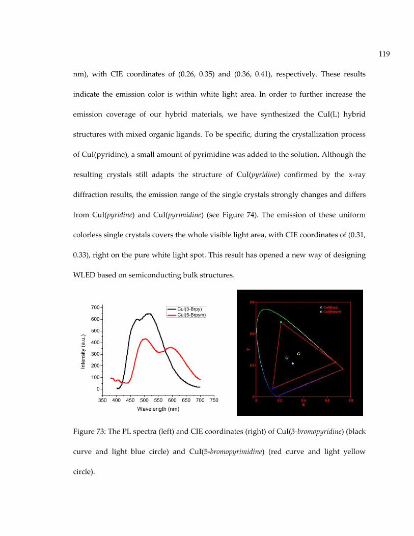
119
nm), with CIE coordinates of (0.26, 0.35) and (0.36, 0.41), respectively. These results
indicate the emission color is within white light area. In order to further increase the
emission coverage of our hybrid materials, we have synthesized the CuI(L) hybrid
structures with mixed organic ligands. To be specific, during the crystallization process
of CuI(pyridine), a small amount of pyrimidine was added to the solution. Although the
resulting crystals still adapts the structure of CuI(pyridine) confirmed by the x-ray
diffraction results, the emission range of the single crystals strongly changes and differs
from CuI(pyridine) and CuI(pyrimidine) (see Figure 74). The emission of these uniform
colorless single crystals covers the whole visible light area, with CIE coordinates of (0.31,
0.33), right on the pure white light spot. This result has opened a new way of designing
WLED based on semiconducting bulk structures.
350 400 450 500 550 600 650 700 750
0
100
200
300
400
500
600
700
Inte
nsity
(a.u
.)
Wavelength (nm)
CuI(3-Brpy) CuI(5-Brpym)
Figure 73: The PL spectra (left) and CIE coordinates (right) of CuI(3-bromopyridine) (black
curve and light blue circle) and CuI(5-bromopyrimidine) (red curve and light yellow
circle).

120
400 450 500 550 600 650 700
0
100
200
300
400
500
600
700
800In
tens
ity (a
.u.)
Wavelength (nm)
CuI(pym) CuI(py) Pym doped CuI(py)
Figure 74: Left: The PL spectra of CuI(pyridine)x(pyrimidine)1-x (blue), CuI(pyridine) (red)
and CuI(pyrimidine) (black). Right: CIE (coordinates) (right)of pyrimidine CuI(pyridine).
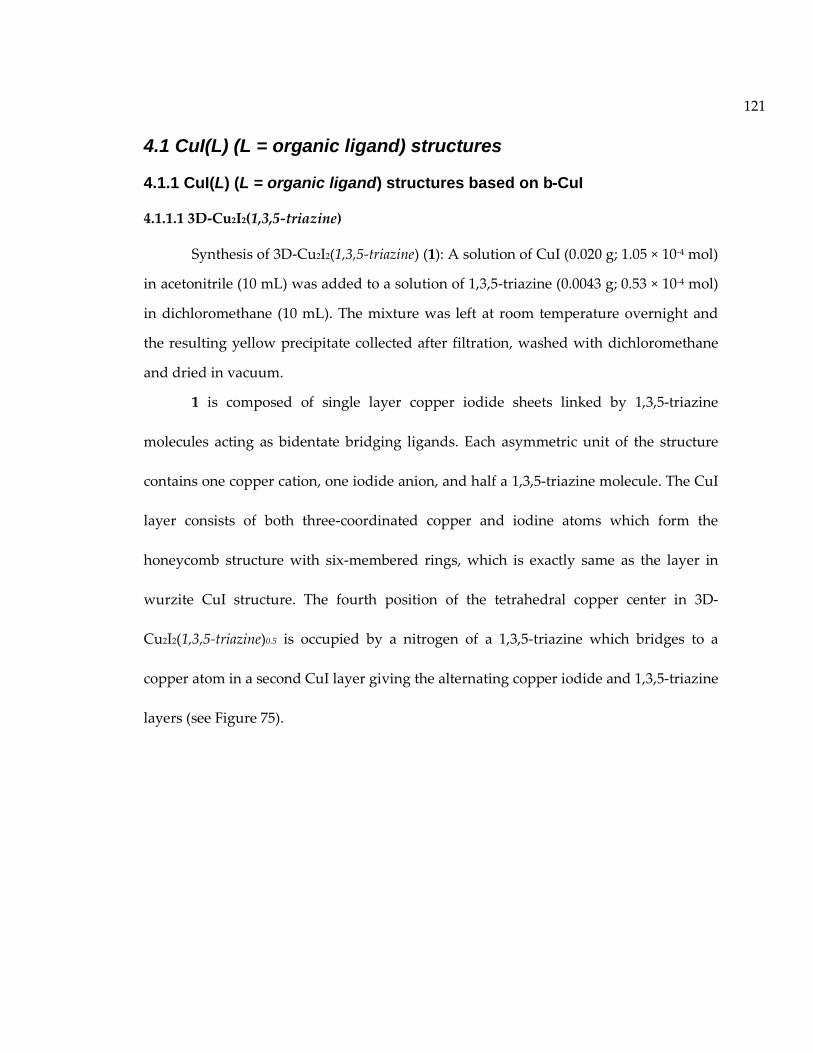
121
4.1 CuI(L) (L = organic ligand) structures
4.1.1 CuI(L) (L = organic ligand) structures based on -CuI
4.1.1.1 3D-Cu2I2(1,3,5-triazine)
Synthesis of 3D-Cu2I2(1,3,5-triazine) (1): A solution of CuI (0.020 g; 1.05 × 10⁻⁴ mol)
in acetonitrile (10 mL) was added to a solution of 1,3,5-triazine (0.0043 g; 0.53 × 10⁻⁴ mol)
in dichloromethane (10 mL). The mixture was left at room temperature overnight and
the resulting yellow precipitate collected after filtration, washed with dichloromethane
and dried in vacuum.
1 is composed of single layer copper iodide sheets linked by 1,3,5-triazine
molecules acting as bidentate bridging ligands. Each asymmetric unit of the structure
contains one copper cation, one iodide anion, and half a 1,3,5-triazine molecule. The CuI
layer consists of both three-coordinated copper and iodine atoms which form the
honeycomb structure with six-membered rings, which is exactly same as the layer in
wurzite CuI structure. The fourth position of the tetrahedral copper center in 3D-
Cu2I2(1,3,5-triazine)0.5 is occupied by a nitrogen of a 1,3,5-triazine which bridges to a
copper atom in a second CuI layer giving the alternating copper iodide and 1,3,5-triazine
layers (see Figure 75).

122
Figure 75: Crystal structures of CuI(1,3,5-triazine)0.5 (Cu: green; I: red; N: blue; C: grey).
X-ray diffraction studies of the as-prepared 3D-CuI(1,3,5-triazine)0.5 samples
indicate the pure phase of the product and high crystallinity. The TG analysis was
performed under N2 protection with a heating rate of 10 ºC/min in the temperature
range 25–450 C. The TG curve of 1 shows that it is thermally stable up to 120 ºC. Above
this temperature, the structure decomposes and only CuI remains. The remaining
weight (84%) is close to the percentage of CuI in the hybrid stucture. (see Figure 76)

123
10 20 30 40 50Two-Theta (deg)
x103
5.0
10.0
15.0In
tens
ity(C
ount
s)
[Cu2I2(triazine).raw] sonication method[3D-Cu2I2(triazine).raw] PowderCell 2.2
80
85
90
95
100
105
Wei
ght (
%)
0 100 200 300 400 500
Temperature (°C)
Sample: Cu2I2triSize: 4.6710 mgMethod: Ramp
TGAFile: C:...\040912\CU2I2TRI(POWDERS).001Operator: SDRun Date: 2011-10-28 09:55Instrument: TGA Q50 V6.3 Build 189
Universal V4.1D TA Instruments
Figure 76: Up: Comparison between experimental and simulated pattern of 3D-
CuI(1,3,5-triazine)0.5. Down: TGA profile of CuI(1,3,5-triazine)0.5.

124
4.1.2 CuI(L) (L = organic ligand) structures based on -CuI
4.1.2.1 1D-CuI(2,6-dimethylpyrazine)
Synthesis of 1D-CuI(2,6-dimethylpyrazine) (2): A solution of CuI (0.190 g; 1mmol)
in saturated potassium iodide solution (2 mL) was added with a solution of 2,6-
dimethylpyrazine (0.108 g; 1mmol) in acetone (2 mL). Acetonitrile (2m) was used as
interlayer between the above two solutions to help crystal growth. The mixture was left
at room temperature overnight and the resulting yellow crystals were collected after
filtration.
In the crystal structure of 2, all Cu(I) atoms in the Cu2I2 ribbon are 3-fold
coordinated to I, and all I atoms bridge to three copper metal centers giving Cu-I
distances varying from 2.6320(7) to 2.6530(6) Å. The Cu2I2 ribbon has same atomic ratio,
valence state and coordination type as its parent rock salt CuI structure. Each 2,6-
dimethylpyrazine binds to one copper atoms via its N sites which completes the fourth
coordination of Cu(I) with a stable and preferred tetrahedral geometry.

125
Figure 77: Crystal structure of CuI(2,6-dimethylpyrazine). (Cu: light blue; I: purple; N:
blue; C: grey)
Comparison between experimental and simulated X-ray diffraction patterns 3D-
CuI(2,6-dimethylpyrazine) indicates the pure phase and high crystallinity of the product.
The TG analysis was performed in N2 atmosphere with a heating rate of 10 ºC/min in
the temperature range 25–450 ºC. The TG curve of 2 shows that it is thermally stable up
to 100 ºC. Above this temperature, the structure decomposes and only CuI remains. The
remaining weight (63%) is close to the percentage of CuI.
10 20 30 40 50Two-Theta (deg)
0
50
100
150
200
250
300
350
SQ
R(C
ount
s)
[CuI(dmpyz).raw][XZ4-74D1.raw]
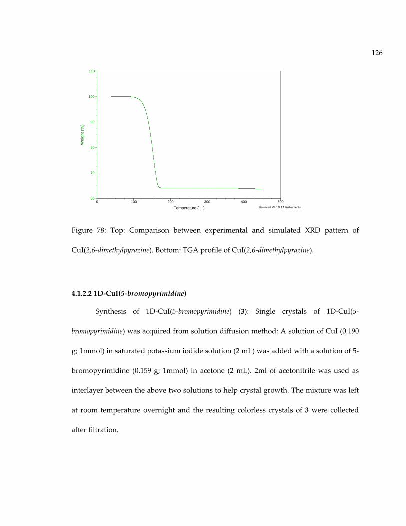
126
Figure 78: Top: Comparison between experimental and simulated XRD pattern of
CuI(2,6-dimethylpyrazine). Bottom: TGA profile of CuI(2,6-dimethylpyrazine).
4.1.2.2 1D-CuI(5-bromopyrimidine)
Synthesis of 1D-CuI(5-bromopyrimidine) (3): Single crystals of 1D-CuI(5-
bromopyrimidine) was acquired from solution diffusion method: A solution of CuI (0.190
g; 1mmol) in saturated potassium iodide solution (2 mL) was added with a solution of 5-
bromopyrimidine (0.159 g; 1mmol) in acetone (2 mL). 2ml of acetonitrile was used as
interlayer between the above two solutions to help crystal growth. The mixture was left
at room temperature overnight and the resulting colorless crystals of 3 were collected
after filtration.
60
70
80
90
100
110
Wei
ght (
%)
0 100 200 300 400 500
Temperature (癈)
Sample: XZ4-60ESize: 4.1800 mg TGA
File: C:...\tga\XZ4-60F.001Operator: QGRun Date: 2012-05-16 10:18Instrument: TGA Q5000 V3.15 Build 263
Universal V4.1D TA Instruments

127
X-ray structural analysis of compound 3 shows that the structure is built from
one-dimensional Cu2I2 double-stranded stair. The asymmetric unit contains one
crystallographically unique tetrahedral Cu+ cation, one unique I− anion and one 5-
bromopyrimidine ligand. The rule of charge balance indicates the valences of Cu to be
+1. All Cu(I) atoms in the Cu2I2 double-stranded stair are 3-fold coordinated to μ3-I−,
and all μ3-I− also bridge to three copper atoms giving Cu–I distances varying from
2.607(3) to 2.675(3) Å.
Figure 79: Crystal structure of CuI(5-bromopyrimidine). (Cu: light blue; I: purple; Br: green;
N: blue; C: grey.)
Comparison between experimental and simulated X-ray diffraction patterns of
the 3D-CuI(5-bromopyrimidine) sample indicates the pure phase and high crystallinity of
the product. The TG analysis was performed under N2 atmosphere with a heating rate of
10 ºC/min in the temperature range 25–450 ºC. The TG curve of 3 shows that it is

128
thermally stable up to 110 ºC. Above this temperature, the structure decomposes and
only CuI remains. The experimental weight (54%) is close to the percentage of 5-
bromopyrimidine in the structure.
10 20 30 40 50Two-Theta (deg)
0
5.0
10.0
15.0
20.0
25.0
30.0
35.0
40.0
SQ
R(C
ount
s)
[GW1-5B.raw][CuI(Brpym).raw]

129
Figure 80: Up: Comparison between experimental and simulated patterns of 3D-CuI(5-
bromopyrimidine)0.5. Down: TGA profile of CuI(5-bromopyrimidine)0.5.
4.1.2.3 1D-CuI(3-iodopyridine)
Synthesis of 1D-CuI(3-iodopyridine) (4): A solution of CuI (0.190 g; 1mmol) in
saturated potassium iodide solution (2 mL) was added with a solution of 3-iodopyridine
(0.205 g; 1mmol) in acetone (2 mL). 2ml acetonitrile was used as interlayer between the
above two solutions to help crystal growth. The mixture was left at room temperature
overnight and the resulting colorless crystals were collected after filtration.
Same as compound 2 and 3, all Cu(I) atoms in the Cu2I2 ladder are 3-fold
coordinated to iodide, and all iodide atoms also bridge to three copper metal centers
giving Cu-I distances varying from 2.6344(6) to 2.6711(7) Å. The Cu2I2 double-stranded
stair can also be regarded as a ribbon that is formed by connecting the two CuI zigzag
single chains via Cu―I bonds.

130
Figure 81: Crystal structures of CuI(3-iodopyridine). (Cu: light blue; I: purple; N: blue; C:
grey)
Comparison between experimental and simulated X-ray diffraction patterns of
3D-CuI(3-iodopyridine) confirms the pure phase of the product. The TG curve of 4 shows
that it is thermally stable up to 100 ºC. Above this temperature, the structure
decomposes and only CuI remains. The remaining weight (49%) is close to the
percentage of CuI in the hybrid structure.

131
10 20 30 40Two-Theta (deg)
0
25
50
75
100
SQ
R(C
ount
s)
[GW1-16E.raw][CuI(3-iodo pyridine).raw]
Figure 82: Up: Comparison between experimental and simulated pattern of 3D-CuI(3-
iodopyridine).Down: TGA profile of CuI(3-iodopyridine).
4.1.2.4 1D-CuI(4-amino-5-iodopyridine)
Synthesis of 1D-CuI(4-amino-5-iodopyridine) (5): A solution of CuI (0.190 g; 1
mmol) in saturated potassium iodide solution (2 mL) was added with a solution of 4-

132
amino-5-iodopyridine (0.220 g; 1 mmol) in acetone (2 mL). 2ml acetonitrile was used as
interlayer between the above two solutions to help crystal growth. The mixture was left
at room temperature overnight and the resulting yellow crystals were collected after
filtration.
Compound 5 crystallizes in the monoclinic structure with space group C2/c. The
asymmetric unit of 5 consists of one Cu, one I and one 4-amino-5-iodopyridine ligand,
each Cu+ ion has a tetrahedral geometry composed of three I- ions and one N from one 4-
amino-5-iodopyridine ligand. The Cu–N distance is 2.031(6) Å, and Cu–I bond lengths
vary from 2.6411(12) to 2.6820(13) Å. The distance between adjacent Cu ions is 2.9154(14)
Å, which shows a weak Cu–Cu interaction.

133
Figure 83: Crystal structures of CuI(4-amino-5-iodopyridine)0.5. (Cu: light blue; I: purple; N:
blue; C: grey).
Comparison between experimental and simulated X-ray diffraction patterns of
the CuI(4-amino-5-iodopyridine) indicate the pure phase of the product and high
crystallinity. The TG analysis was protected by N2 gas with a heating rate of 10 ºC/min
in the temperature range 25–450 ºC. The TG curve of 5 shows that it is thermally stable
up to 100 ºC. Above this temperature, the structure decomposes and only CuI remains.
The remaining weight (47.4%) is close to the percentage of CuI.
10 20 30 40 50Two-Theta (deg)
0
25
50
75
100
125
SQ
R(C
ount
s)
[GW1-16J.raw][CuI(3-iodo 5-amino pyridine).raw]

134
Figure 84: (a) Comparison between experimental and simulated patterns of 3D-CuI(4-
amino-5-iodopyridine).(b) TGA profile of CuI(4-amino-5-iodopyridine).
4.1.2.5 1D-CuI(3-bromopyridine)
Synthesis of 1D-CuI(3-bromopyridine) (6): Pure phase of compound 6 was
obtained from a mixture of CuI (0.019 g; 0.1 mmol), 5-bromopyrimidine (0.016 g; 0.1
mmol) and 3 ml acetonitrile. After leaving the mixture over night, the pure white
powder of 6 precipitated from solution.
Single crystals of 6 were acquired when a solution of CuI (0.190 g; 1 mmol) in
saturated potassium iodide solution (2 mL) was added with a solution of 3-
bromopyridine (0.158 g; 1 mmol) and 3-chloropyridine (0.113 g; 0.1 mmol) in acetone (2
mL). 2 ml of acetonitrile was used as interlayer between the above two solutions to help
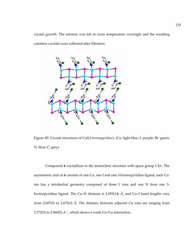
135
crystal growth. The mixture was left at room temperature overnight and the resulting
colorless crystals were collected after filtration.
Figure 85: Crystal structures of CuI(3-bromopyridine). (Cu: light blue; I: purple; Br: green;
N: blue; C: grey)
Compound 6 crystallizes in the monoclinic structure with space group C2/c. The
asymmetric unit of 6 consists of one Cu, one I and one 3-bromopyridine ligand, each Cu+
ion has a tetrahedral geometry composed of three I- ions and one N from one 3-
bromopyridine ligand. The Cu–N distance is 2.055(14) Å, and Cu–I bond lengths vary
from 2.607(3) to 2.675(3) Å. The distance between adjacent Cu ions are ranging from
2.772(5) to 2.960(5) A ˚, which shows a weak Cu–Cu interaction.
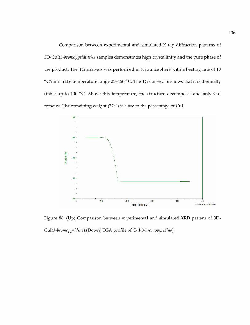
136
Comparison between experimental and simulated X-ray diffraction patterns of
3D-CuI(3-bromopyridine)0.5 samples demonstrates high crystallinity and the pure phase of
the product. The TG analysis was performed in N2 atmosphere with a heating rate of 10
ºC/min in the temperature range 25–450 ºC. The TG curve of 6 shows that it is thermally
stable up to 100 ºC. Above this temperature, the structure decomposes and only CuI
remains. The remaining weight (37%) is close to the percentage of CuI.
Figure 86: (Up) Comparison between experimental and simulated XRD pattern of 3D-
CuI(3-bromopyridine).(Down) TGA profile of CuI(3-bromopyridine).

137
4.1.2.6 Pyrimidine substituted 1D-CuI(pyridine)
Synthesis of pyrimidine doped 1D-CuI(pyridine) (7): Pure phase of compound 7
was obtained by adding bromopyrimidine (0.016 g; 0.1mmol) in 1ml of acetone drop by
drop into a solution of CuI (0.019 g; 0.1mmol) in 2ml of saturated potassium iodide
solution. The pure white powder of 7 immediately precipitated from solution.
Single crystals of 7 were acquired when a solution of CuI (0.190 g; 1 mmol) in
saturated potassium iodide solution (2 mL) was added to a solution of pyridine (0.079 g;
1 mmol) and pyrimidine (0.004 g; 0.05 mmol) in acetone (2 mL). The mixture was left in
the solution at room temperature overnight resulting in colorless crystals.
Figure 87: Crystal structure of CuI(pyridine). (Cu: light blue; I: purple; N: blue; C: grey)

138
Comparison between experimental pattern of pyrimidine substituted
CuI(pyridine) and simulated pattern of CuI(pyridine) suggest the substituted compound
has the same structure as CuI(pyridine). The TG analysis was performed in N2
atmosphere with a heating rate of 10 ºC/min in the temperature range 25–450 ºC. The
TG curve of 7 shows that it is thermally stable up to 80 ºC. Above this temperature, the
structure decomposes and only CuI remains. The remaining weight (71%) is close to the
percentage of CuI.

139
10 20 30 40 50Two-Theta (deg)
0
10
20
30
40
50
60S
QR
(Co
un
ts)
[GW1-32A_white light.raw][CUIPYS.raw]
Figure 88: (a) Comparison between experimental pattern of pyrimidine substituted
CuI(pyridine) and simulated pattern of CuI(pyridine).(b) TGA profile of pyrimidine
substituted CuI(pyridine).

140
4.2 Optical absorption and emission properties of CuI(L) (L =organic ligand)
4.2.1 3D-CuI(1,3,5-triazine)0.5
The optical absorption spectra of CuI and CuI(1,3,5-triazine)0.5 were measured by
diffuse reflectance experiments at room temperature with a Shimadzu UV-3101PC
double beam, double monochromator spectrophotometer. Data were collected in the
wavelength range of 300-800 nm and converted using the Kubelka-Munk function.
BaSO4 powder was used as a standard (100% reflectance). The scattering coefficient (S)
was treated as a constant since the average particle size of the samples used in the
measurements was greatly larger than 5 nm, and the results are plotted in Figure 89. The
absorption edges of Cu2I2(1,3,5-triazine) are found to be 2.5 eV. Compared to the
measured value of 3.0 eV for β-CuI, it clearly indicates a significant red shift.
Figure 89: Optical absorption of CuI and CuI(1,3,5-triazine)0.5.

141
In order to understand the optical absorption behavior of Cu2I2(1,3,5-triazine),
DFT calculation were performed on both CuI and Cu2I2(1,3,5-triazine). The band gap
structures of both compounds are shown in Figure 90 and Figure 91. The calculated
band structure of CuI indicates the direct band gap of 0.991 eV, about 2 eV lower than its
experimental band gap. For Cu2I2 (1,3,5-triazine), it shows direct band gap of 0.835 eV,
which is also about 2 eV lower than its experimental value. The relative band gap value
between two compounds from calculation is consistent with their experimental value.
Figure 90: Band structure of CuI from DFT calculation.
(
b)

142
Figure 91: Band structure of Cu2I2 (1,3,5-triazine) from DFT calculation.
Density of states (DOS) analysis has revealed some interesting information about
the composition of the bands. As shown in Figure 93(a), the valence band is mainly
contributed by the Cu (3d), I (5p) and Cu (4p) orbitals from inorganic module and the
band shape is similar to the valance band shape of CuI (see Figure 92), while the
conduction band is mainly contributed by the atomic orbitals of C (2p) and N (2p) from
organic ligands (see Figure 93(b)). There is another continuous energy band above
conduction band energy level and its band shape is similar to CuI conduction band and
is mostly contributed by the atomic orbitals of inorganic modules such as Cu (4s), Cu
(4d), Cu(3p) and I(5s). The energy gap between two “inorganic bands” (valence band
and the band above conduction band) is about 2.9eV (2.9eV – 0eV), about 1.9 eV higher
than 0.991 eV of CuI band gap. These results may be explained by quantum
(
a)
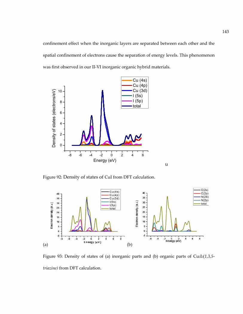
143
confinement effect when the inorganic layers are separated between each other and the
spatial confinement of electrons cause the separation of energy levels. This phenomenon
was first observed in our II-VI inorganic organic hybrid materials.
-8 -6 -4 -2 0 2 4 6
0
2
4
6
8
10
Energy (eV)
Den
sity
of s
tate
s (e
lect
rons
/eV)
Cu (4s) Cu (4p) Cu (3d) I (5s) I (5p) total
u
Figure 92: Density of states of CuI from DFT calculation.
(a) (b)
Figure 93: Density of states of (a) inorganic parts and (b) organic parts of Cu2I2(1,3,5-
triazine) from DFT calculation.

144
Figure 94 shows the photoluminescence of Cu2I2(1,3,5-triazine) and CuI with the
excitation wavelength of 320 nm. Compared to the sharp peak of CuI at 410nm, the
Cu2I2(1,3,5-triazine) shows a broad PL coverage ranging from 470 nm to 750 nm, covering
much of visible light area.
350 400 450 500 550 600 650 700 750 800
0
200
400
600
800
1000
Inte
nsity
(a.u
.)Wavelength (nm)
Figure 94: Photoluminesence of Cu2I2(triazine) and CuI with the excitation wavelength of
320 nm.
4.2.2 1D-CuI(L)
The optical absorption and emission behavior were also tested on 1D-CuI(L)
structures, the parent structure of which is -CuI. The results are summarized in Table
13. Keeping the 1D chain inorganic module intact, the band gap has been systematically
tuned from 2.2 eV to 3.2 eV just by changing organic ligands. The starting wavelengths
in PL spectra of these materials are strongly related to their band gap. The structure with
larger band gap generally have lower starting wavelength in its PL spectrum. When the
numbers of starting wavelengths are transferred to electron voltages using Einstein's
photoelectric equation, the values are just a little larger than their relative band gap.

145
These results again suggest that 1D-CuI(L) inorganic organic hybrid semiconductors
exhibit band gap emission.
Table 13: Summary of optical absorption and emission behavior of 1D-CuI(L) inorganic
organic hybrid structures.
Structures Band
Gap
Emission
Peak (nm)
Emission
Range(nm)
Emission Color
CuI(2,6-dimethylpyrazine) 2.2 eV 500 (C) 460-580 yellow
CuI(pyrimidine) 2.6 eV 525 (C) 470-670 green
CuI(5-bromopyrimidine) 2.5 eV 500,610nm 440-700 yellow white
CuI(3-iodopyrimidine) 2.8 eV NA NA NA
CuI(3-bromopyridine) 2.8 eV 450,530 400-650 blue white
CuI(pyridine) 3.0 eV 450 380-550 light Blue
CuI(4-amino-5-
iodopyrimidine)
3.2 eV NA NA NA

146
(a)1 2 3 4 5
0.0
0.5
1.0
1.5
2.0
2.5
3.0
3.5
Energy (eV)
KM F
unct
ion
(b)1 2 3 4
0.5
1.0
1.5
Energy (eV)
KM F
unct
ion
(c)1.5 2.0 2.5 3.0 3.5 4.0 4.5
0.0
0.5
1.0
1.5
2.0
2.5
Inte
nsity
(a.u
.)
Energy (eV) (d)1.5 2.0 2.5 3.0 3.5 4.0 4.5
0.0
0.5
1.0
1.5
2.0
2.5
3.0
3.5
4.0
Inte
nsity
(a.u
.)
Energy (eV)
(e)1.5 2.0 2.5 3.0 3.5 4.0 4.5
0.0
0.2
0.4
0.6
0.8
1.0
1.2
1.4
1.6
Energy (eV)
KM
Fun
ctio
n
(f)1.5 2.0 2.5 3.0 3.5 4.0 4.5
0.0
0.5
1.0
1.5
2.0
2.5
3.0
3.5
4.0
KM F
unct
ion
Energy (eV)
(g)1.0 1.5 2.0 2.5 3.0
0.0
0.5
1.0
1.5
2.0
KM F
unct
ion
Energy (eV)

147
Figure 95: The optical absorption behavior of (a) CuI(4-amino-5-iodopyridine), (b) CuI(3-
iodopyridine), (c) CuI(3-iodopyridine), (d) CuI(pyrdine), (e) CuI(5-bromopyrimidine), (f)
CuI(pyrimidine) and (g) CuI(2,6-dimethylpyrazine).
DFT calculation was performed on the selected compounds CuI(4-amino-5-
iodopyridine) and CuI(2,6-dimethylpyrazine) to understand their band structures.
The calculated band gap of CuI(4-amino-5-iodopyridine) is 1.8 eV, 1.5 eV less than
its experimental value, which is common for DFT calculation. A closer look at the
density of states reveals that the valence band of CuI(4-amino-5-iodopyridine) mainly
consists of the 3d orbitals of copper and the 5p orbitals of iodide (see Figure 96), while
the conduction band is mainly contributed by the 2p orbitals of carbon and nitrogen
atoms. The results suggest that the band gap absorption and emission processes of
CuI(4-amino-5-iodopyridine) involves charge transfer between the organic molecules and
the inorganic CuI modules.
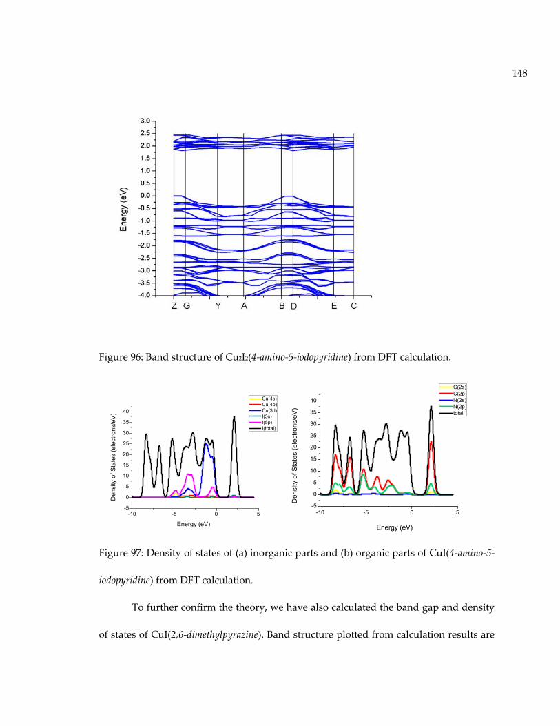
148
Figure 96: Band structure of Cu2I2(4-amino-5-iodopyridine) from DFT calculation.
-10 -5 0 5-5
0
5
10
15
20
25
30
35
40
Den
sity
of S
tate
s (e
lect
rons
/eV)
Energy (eV)
Cu(4s) Cu(4p) Cu(3d) I(5s) I(5p) I(total)
-10 -5 0 5-5
0
5
10
15
20
25
30
35
40
Den
sity
of S
tate
s (e
lect
rons
/eV
)
Energy (eV)
C(2s) C(2p) N(2s) N(2p) total
Figure 97: Density of states of (a) inorganic parts and (b) organic parts of CuI(4-amino-5-
iodopyridine) from DFT calculation.
To further confirm the theory, we have also calculated the band gap and density
of states of CuI(2,6-dimethylpyrazine). Band structure plotted from calculation results are

149
shown in Figure 98, which demonstrates the indirect band gap of CuI(2,6-
dimethylpyrazine). The calculated value of its band gap is 0.991 eV, about 1.3eV less than
its experimental value. The density of states diagram of CuI(2,6-dimethylpyrazine)
resembles that of CuI(4-amino-5-iodopyridine). The valence band of CuI(4-amino-5-
iodopyridine) is also composed of the 3d orbitals of copper and the 5p orbitals of iodide
(see Figure 99), while the conduction band is made of the 2p orbitals of both carbon and
nitrogen atoms. This result further confirms the band gap absorption in 1D-CuI(L)
involves charge transfer from HOMO of CuI modules to the LUMO of organic molecules.
Figure 98: Band structure of CuI(2,6-dimethylpyrizine) from DFT calculation.

150
-10 -5 0 5-5
0
5
10
15
20
25
30
35
40
Energy (eV)
Den
sity
of S
tate
s (e
lect
rons
/eV
) Cu(4s) Cu(4p) Cu(3d) I(5s) I(5p) total
-10 -9 -8 -7 -6 -5 -4 -3 -2 -1 0 1 2 3 4 5-5
0
5
10
15
20
25
30
35
40
Den
sity
of S
tate
s (e
lect
rons
/eV
)
Energy (eV)
C(2s) C(2p) N(2s) N(2p) total
Figure 99: Density of states of (a) inorganic parts and (b) organic parts of CuI(2,6-
dimethylpyrizine) from DFT calculation.
To further understand the impact of LUMO energy levels of organic ligands on
the band gap of 1D-CuI(L) inorganic organic hybrid structures, we have also calculated
the HOMO and LUMO energy levels of different organic ligands on Guassian [09] with
the hybrid functional: [B3LYP]. Three basis sets, 3-21G, 6-311+G and DGDZVP were
used for the calculation and results are listed in Table 13. The 3-21G basis set is smaller
than 6-311+G* and DGDZVP, so the results can only be used as rough comparison.
Although the 6-311+G* basis set is more accurate than 3-21G, it is not suitable in
calculating the molecules containing fifth row element such as iodine. DGDZVP (density
Guass double-zeta with polarization functions) is a full-electron basis set that contains 36
basis functions and 114 Guassian primitive functions. And it has been demonstrated
giving better results in terms of describing the geometries of iodine-containing
compounds than basis sets with pseudopotential. Therefore DGDZVP basis set is most

151
suitable in calculating the listed organic molecules. The calculation results demonstrate
the significant correlation between the electronic affinity of functional groups and the
energy levels of HOMO and LUMO as show in Table 14. To be specific, molecules (i) -
(v) are pyridine and its derivatives. For the molecule (iii) – (v), there is only halide group
(I, Br, Cl) on the pyridine ring. The electron withdrawing effect of halide group in these
structures declines both the HOMO and LUMO energy levels compared to pyridine. In
contrary, when an electron donating group such as amino group is further attached to
the pyridine ring, as in case (ii), the HOMO and LOMO energy levels become higher
than pyridine. Similar phenomena are also observed in pyrimidine’s and pyrazine’s
derivatives. For example, 2,6-dimethylpyrazine (vii) has two methyl groups (electron
donating functional group) on the pyrazine framework, and its LUMO and HOMO are
higher than pyrazine (viii). The 5-bromopyrimidine (ix) has electron withdrawing
bromo group attached to pyrimidine ring and its energy levels become lower than
pyrimidine (vi). These results can be summarized as both HOMO and LUMO energy
levels of aromatic molecules are decreased by electron withdrawing functional group
and increased by electron donating functional group.
Based on this conclusion and the idea that the energy levels of conduction bands
of 1D-CuI(L) structures are then determined by LUMO energy level of organic ligands,
we have proposed a method to tune the band gap absorption and emission behavior of
1D-CuI(L) inorganic organic semiconductors. We maintain the one dimensional CuI
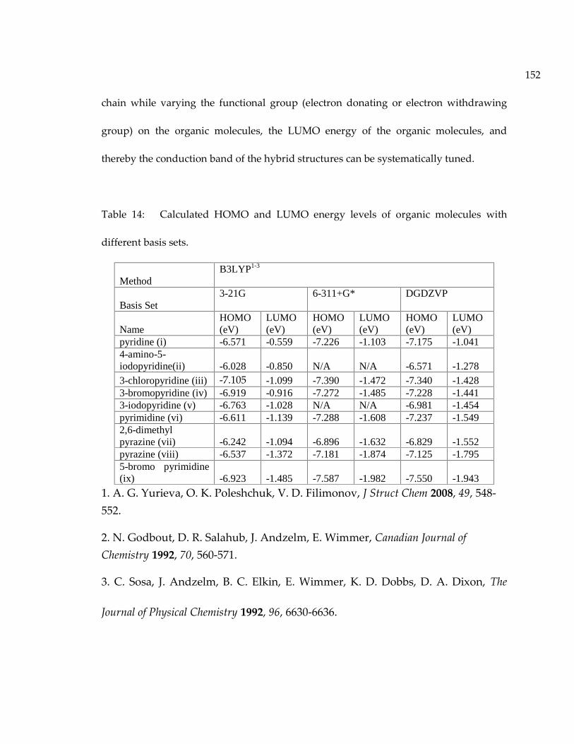
152
chain while varying the functional group (electron donating or electron withdrawing
group) on the organic molecules, the LUMO energy of the organic molecules, and
thereby the conduction band of the hybrid structures can be systematically tuned.
Table 14: Calculated HOMO and LUMO energy levels of organic molecules with
different basis sets.
MethodB3LYP1-3
Basis Set3-21G 6-311+G* DGDZVP
NameHOMO(eV)
LUMO(eV)
HOMO(eV)
LUMO(eV)
HOMO(eV)
LUMO(eV)
pyridine (i) -6.571 -0.559 -7.226 -1.103 -7.175 -1.0414-amino-5-iodopyridine(ii) -6.028 -0.850 N/A N/A -6.571 -1.2783-chloropyridine (iii) -7.105 -1.099 -7.390 -1.472 -7.340 -1.4283-bromopyridine (iv) -6.919 -0.916 -7.272 -1.485 -7.228 -1.4413-iodopyridine (v) -6.763 -1.028 N/A N/A -6.981 -1.454pyrimidine (vi) -6.611 -1.139 -7.288 -1.608 -7.237 -1.5492,6-dimethylpyrazine (vii) -6.242 -1.094 -6.896 -1.632 -6.829 -1.552pyrazine (viii) -6.537 -1.372 -7.181 -1.874 -7.125 -1.7955-bromo pyrimidine(ix) -6.923 -1.485 -7.587 -1.982 -7.550 -1.943
1. A. G. Yurieva, O. K. Poleshchuk, V. D. Filimonov, J Struct Chem 2008, 49, 548-552.
2. N. Godbout, D. R. Salahub, J. Andzelm, E. Wimmer, Canadian Journal ofChemistry 1992, 70, 560-571.
3. C. Sosa, J. Andzelm, B. C. Elkin, E. Wimmer, K. D. Dobbs, D. A. Dixon, The
Journal of Physical Chemistry 1992, 96, 6630-6636.

153
This idea has been tested by comparing the experimental band gap and the PL
spectra of the new 1D-CuI(L) structures with the calculated LUMO energy level of their
ligands. The results are summarized in Table 15. The band gap of these structures
increase in the order of 3 < 4 < 5 < 7 < 6 and the starting wavelengths decrease in the
order of 7 > 4 > 3 (5 and 6 are not fluorescent), similar to the calculated LUMO trend of 4
< 3 < 5 < 7 < 6. This result further validates our hypothesis.
Table 15: The comparison between the band gap of 1D-CuI(L) structures, calculated
LUMO energy level at B3LYP/DGDZVP and emission range.
1D-CuI(L) structures Band Gap Calculated
LUMO position
PL emission range
CuI(2,6-dimethylpyrazine) (2) 2.2 eV -1.552 460-580nm
CuI(5-bromopyrimidine) (3) 2.5 eV -1.943 440-700nm
CuI(3-iodopyrimidine) (4) 2.8 eV -1.454 NA
CuI(3-bromopyridine)(6) 2.8 eV -1.441 400-650nm
CuI(4-amino-5-
iodopyrimidine) (5)
3.2 eV -1.278 NA
During the fluorescence measurement of new CuI(L) inorganic organic hybrid
structures, we found the ligands with bromo group such as 3-bromopyridine and 5-

154
bromopyrimidine can give wide and balanced spectra. Compared to other CuI(L)
compounds with single and sharp emission peak, both the CuI(Br-pyridine) and CuI(Br-
pyrimidine) display double peaks which cover more than 250 nm out of 300 nm in the
visible light range (400 nm-700 nm). The CIE calculation gives (0.26, 0.35) for CuI(Br-
pyridine) and (0.36, 0.41) for CuI(Br-pyrimidine) as their CIE coordinates. These results
indicate the emission color is already within white light area.
(a) (b)
(c)
Figure 100: The PL spectra (left) and CIE coordinates (right) of CuI(3-bromopyridine)
(black curve and light blue circle) and CuI(5-bromopyrimidine) (red curve and light

155
yellow circle). (c) Logo made from white light emitting pyrimidine substituted
CuI(pyridine) powders.
To further increase the white light coverage, we have tried to synthesize CuI(L)
structures with mixed ligands. CuI(pyrimidine) and CuI(pyridine) show 0.3 eV difference
of band gap as shown in Figure 101. The reason of the difference is that LUMO energy
level of pyridine is higher than that of pyrimidine. There are two electron-rich nitrogen
atoms in the aromatic ring of pyrimidine compared to one nitrogen atom in pyridine
and it cause both HOMO and LUMO energy levels in pyrimidine to increase. The PL
spectra show the emission range of CuI(pyrimidine) and CuI(pyridine) start from 400nm
and 460 nm, respectively, corresponding to their band gap values. The emission
intensity is strong, but both compounds suffer from the narrow coverage. To solve the
problem, we have prepared pyrimidine substituted CuI(pyridine) as discussed in
previous chapter. The colorless crystals of substituted compounds have same XRD
pattern as unsubstituted CuI(pyridine) structure and it does not show changes in UV
spectrum either. However, the emission from the crystals surprisingly covers the whole
visible light area from 400 nm to 700 nm, giving CIE coordinates (0.31, 0.33), right on the
pure white light spot. The Color Rendering Index (CRI) and Correlated Color
Temperature (CCT) of the compound are computed to be 87.4 and 6455K, indicating its
strong ability to reproduce the colors of various objects faithfully.

156
1.5 2.0 2.5 3.0 3.5 4.0 4.50.0
0.5
1.0
1.5
2.0
2.5
3.0
3.5
4.0KM
Fun
ctio
n
Energy (eV)1.5 2.0 2.5 3.0 3.5 4.0
0.0
0.2
0.4
0.6
0.8
1.0
1.2
KM
Fun
ctio
n
Wavelength (nm)
Figure 101: The optical absorption spectrum of CuI(pyrimidine)0.5 (left) and CuI(pyridine)
(right).
(a) (b)
(c)

157
(d)
(e)
Figure 102: (a): The PL spectra of pyrimidine substituted CuI(pyridine) (blue),
CuI(pyridine) (red) and CuI(pyrimidine) (black). (b): CIE coordinates of pyrimidine
substituted CuI(pyridine). (c) Logo made from white light emitting pyrimidine
substituted CuI(pyridine) powders. (d) Comparison between white light emitting
pyrimidine substituted CuI(pyridine) crystal with other 1D-CuI(L) crystals under the UV
light. (e) Comparison between white light emitting pyrimidine substituted CuI(pyridine)
crystal with other 1D-CuI(L) crystals under the ambient light.

158
4.4 Mechanochromic properties of CuI(L) (L = organic ligand)
During the process of investigating luminescence properties of hybrid materials
based on 1D-CuI(L) inorganic organic hybrid semiconductors, we have also discovered
mechanochromic properties in CuI(2,6-dimethylpyrazine) and CuI(pyrimidine).
The CuI(2,6-dimethylpyrazine) cluster is a light yellow powder under ambient
light. Under UV irradiation (peak wavelength at 365 nm), the structure gives strong
yellow emission as shown in Figure 103. The mechanochromic properties were observed
when grinding the samples in mortar. The yellow emission becomes red under UV light
after grinding.
Solid state emission was recorded for the cluster before and after grinding at
room temperature. For the crystals before grinding, a broad emission band is observed
at max = 530 nm under excitation at ex = 365 nm. This is in agreement with the observed
yellow emission. After grinding, a broad emission band is observed at max = 625 nm (ex
= 360 nm) in agreement with the red emission. Comparison between the XRD patterns
before and after griding suggest the structural change under the applied pressure when
grinding.

159
Figure 103: Photos showing the photoluminescence change of CuI(2,6-dimethylpyrazine)
after (left) and before (right) griding.
450 500 550 600 650 700
0
20
40
60
80
100
120
140
Inte
nsity
(a.u
.)
Wavelength (nm)
CuI(dmpyz) Before grinding After Grinding
1.5 2.0 2.5 3.0 3.5 4.0
0.0
0.5
1.0
1.5
2.0
2.5
3.0
Wavelength (nm)
KM F
unct
ion
Before grinded After grinded
Figure 104: (left) PL changes of CuI(2,6-dimethylpyrazine) before and after grinding. (right)
UV changes of CuI(2,6-dimethylpyrazine) before and after grinding.

160
10 20 30 40 50Two-Theta (deg)
0
50
100
150
SQ
R(C
ount
s)
[PC1-19A_crystal.raw][PC1-19A_powder.raw]
Figure 105: Comparison of XRD patterns before (black) and after (red) griding.
Another compound showing the mechanochromic property is the
CuI(pyrimidine)0.5. The CuI(pyrimidine)0.5 crystals is shining with green light under
ambient light. At room temperature and under UV lamp irradiation (peak wavelength at
365 nm), a strong orange emission was observed as shown in Figure 106. The
mechanochromic properties were observed when grinding the samples in mortar. The
green emission becomes orange under UV light after grinding.
Solid state emission was recorded for the cluster before and after grinding at
room temperature. For the crystals before grinding, a broad emission band is observed
at max = 500 nm under excitation at ex = 365 nm. This is in agreement with the yellow
emission observed. After grinding, the original emission peak decease while another
peak is observed at max = 610 nm (ex = 360 nm) in agreement with the orange emission

161
observed. Comparison of XRD patterns before and after griding suggest the structural
change under the applied pressure when grinding.
Figure 106: Photos showing the luminescence change of CuI(2,6-dimethylpyrazine) after
and before griding.
400 450 500 550 600 650 700
0
50
100
150
200
Inte
nsity
(a.u
.)
Wavelength (nm)
CuI(pym) Before griding After Griding
1.5 2.0 2.5 3.0 3.50
1
2
3
4
Wavelength (nm)
KM F
unct
ion
After GrindingBefore Grinding
Figure 107: (left) PL changes of CuI(2,6-dimethylpyrazine) before and after grinding. (right)
UV changes of CuI(2,6-dimethylpyrazine) before and after grinding.

162
10 20 30 40 50Two-Theta (deg)
0
50
100
150
200
SQR
(Cou
nts)
[XZ4-74A_crystal.raw][XZ4-74A_powder.raw]
Figure 108: Comparison of XRD patterns before (black) and after (red) griding.
4.4 Summary
In summary, we have developed a novel class of I-VII inorganic organic hybrid
semiconductors. A number of new 1D-CuI(L) (L = organic ligand) inorganic organic
hyrbid materials were acquired under solvent diffusion method and their crystal
structures were solved. The 1D-CuI(L) hybrid structures display tunable optical
absorption and emission behavior and some of the structures such as CuI(3-
bromopyridine) and CuI(5-bromopyrimidine) are able to give close-to–white-light
photoluminesence. The DFT calulation results of selected 1D-CuI(L) structures show that
the valance band is contributed by the atomic orbitals in inorganic modules while the

163
conduction band is determined by LUMO of organic ligands. By adjusting the functional
group on the organic molecules, their LUMO energy levels as well as the band gap of
hybrid structures can be systematically tuned. This discovery further lead us to design
1D-CuI(L) structures with mixed ligand to get white light emission. Eventually, we have
prepared pyrimidine substituted CuI(pyridine) crystals which can emit strong and pure
white light with CIE coordinates of (0.31, 0.33).

164
References
(1) Mitzi, D. B. Adv Mater 2009, 21, 3141.(2) Ingham, B.; Chong, S. V.; Tallon, J. L. J. Phys. Chem. B 2005, 109, 4936.(3) Chen, D. L.; Wen, H. J.; Chen, H. M.; Wang, H. L.; Zhang, R.; Xu, H. L.; Yang, D.
Y.; Lu, H. X. Mater. Chem. Phys. 2009, 116, 507.(4) Gauthron, K.; Lauret, J. S.; Doyennette, L.; Lanty, G.; Al Choueiry, A.; Zhang, S. J.;
Brehier, A.; Largeau, L.; Mauguin, O.; Bloch, J.; Deleporte, E. Opt Express 2010, 18,5912.
(5) Wu, M.; Rhee, J.; Emge, T. J.; Yao, H. B.; Cheng, J. H.; Thiagarajan, S.; Croft, M.;Yang, R. G.; Li, J. Chem. Commun. 2010, 46, 1649.
(6) Huang, X. Y.; Li, J.; Fu, H. X. J. Am. Chem. Soc. 2000, 122, 8789.(7) Huang, X. Y.; Li, J.; Zhang, Y.; Mascarenhas, A. J. Am. Chem. Soc. 2003, 125, 7049.(8) Huang, X. Y.; Li, J. J. Am. Chem. Soc. 2007, 129, 3157.(9) Huang, X. Y.; Roushan, M.; Emge, T. J.; Bi, W. H.; Thiagarajan, S.; Cheng, J. H.;
Yang, R. G.; Li, J. Angew Chem Int Edit 2009, 48, 7871.(10) Yao, H. B.; Zhang, X. A.; Wang, X. H.; Yu, S. H.; Li, J. Dalton T 2011, 40, 3191.(11) Roushan, M.; Zhang, X.; Li, J. Angew Chem Int Edit 2012, 51, 436.(12) Ki, W.; Li, J. Journal of the American Chemical Society 2008, 130, 8114.(13) Sleight, A. W. Endeavour 1995, 19.(14) Zhang, Y.; Islam, Z.; Ren, Y.; Parilla, P. A.; Ahrenkiel, S. P.; Lee, P. L.;
Mascarenhas, A.; McNevin, M. J.; Naumov, I.; Fu, H. X.; Huang, X. Y.; Li, J. PhysRev Lett 2007, 99.
(15) Jing Li, W. B., Wooseok Ki, Xiaoying Huang, and Srihari Reddy J. Am. Chem. Soc.2007, 129 14140.
(16) Zhang, X.; Ren, Y.; Roushan, M.; Li, J. Eur J Inorg Chem 2012, 5966.(17) Chernova, N. A.; Roppolo, M.; Dillon, A. C.; Whittingham, M. S. J. Mater. Chem.
2009, 19, 2526.(18) Zheng, H. D.; Ou, J. Z.; Strano, M. S.; Kaner, R. B.; Mitchell, A.; Kalantar-Zadeh,
K. Adv. Funct. Mater. 2011, 21, 2175.(19) Esposito, D. V.; Forest, R. V.; Chang, Y. C.; Gaillard, N.; McCandless, B. E.; Hou,
S. Y.; Lee, K. H.; Birkmire, R. W.; Chen, J. G. G. Energ Environ Sci 2012, 5, 9091.(20) Tacca, A.; Meda, L.; Marra, G.; Savoini, A.; Caramori, S.; Cristino, V.; Bignozzi, C.A.; Pedro, V. G.; Boix, P. P.; Gimenez, S.; Bisquert, J. Chemphyschem 2012, 13, 3025.(21) Mao, A.; Kim, J. K.; Shin, K.; Wang, D. H.; Yoo, P. J.; Han, G. Y.; Park, J. H. J
Power Sources 2012, 210, 32.(22) Mi, Q. X.; Zhanaidarova, A.; Brunschwig, B. S.; Gray, H. B.; Lewis, N. S. Energ
Environ Sci 2012, 5, 5694.(23) Ho, G. W.; Chua, K. J.; Siow, D. R. Chem Eng J 2012, 181, 661.(24) Zhang, K.; Shi, X. J.; Kim, J. K.; Park, J. H. Phys Chem Chem Phys 2012, 14, 11119.

165
(25) Liu, X.; Wang, F. Y.; Wang, Q. Phys Chem Chem Phys 2012, 14, 7894.(26) Goncalves, R. H.; Leite, L. D. T.; Leite, E. R. Chemsuschem 2012, 5, 2341.(27) Hsiao, P. T.; Chen, L. C.; Li, T. L.; Teng, H. S. J Mater Chem 2011, 21, 19402.(28) Su, J. Z.; Feng, X. J.; Sloppy, J. D.; Guo, L. J.; Grimes, C. A. Nano Lett 2011, 11, 203.(29) Ishihara, H.; Kannarpady, G. K.; Khedir, K. R.; Woo, J.; Trigwell, S.; Biris, A. S.
Phys Chem Chem Phys 2011, 13, 19553.(30) Bar, M.; Weinhardt, L.; Marsen, B.; Cole, B.; Gaillard, N.; Miller, E.; Heske, C.
Appl Phys Lett 2010, 96.(31) Alexander, B. D.; Kulesza, P. J.; Rutkowska, L.; Solarska, R.; Augustynski, J. J
Mater Chem 2008, 18, 2298.(32) Wang, H. L.; Deutsch, T.; Turner, J. A. J Electrochem Soc 2008, 155, F91.(33) Gratzel, M. Nature 2001, 414, 338.(34) Santato, C.; Ulmann, M.; Augustynski, J. J. Phys. Chem. B 2001, 105, 936.(35) Zheng, H. D.; Tachibana, Y.; Kalantar-zadeh, K. Langmuir 2010, 26, 19148.(36) Xia, Q.; Zhao, H. L.; Du, Z. H.; Wang, J.; Zhang, T. H.; Wang, J.; Lv, P. P. J Power
Sources 2013, 226, 107.(37) Fu, X. M. Rare Metal Mat Eng 2012, 41, 488.(38) Sasidharan, M.; Gunawardhana, N.; Noma, H.; Yoshio, M.; Nakashima, K. B Chem
Soc Jpn 2012, 85, 642.(39) Tang, W.; Liu, L. L.; Zhu, Y. S.; Sun, H.; Wu, Y. P.; Zhu, K. Energ Environ Sci 2012,
5, 6909.(40) Meduri, P.; Clark, E.; Kim, J. H.; Dayalan, E.; Sumanasekera, G. U.; Sunkara, M. K.
Nano Lett 2012, 12, 1784.(41) Liang, Q. Q.; Li, Y. M.; Li, J. H. J Nanosci Nanotechno 2012, 12, 2839.(42) Saji, V. S.; Lee, C. W. Chemsuschem 2012, 5, 1146.(43) Sen, U. K.; Mitra, S. Rsc Adv 2012, 2, 11123.(44) Li, S.; Han, C. H.; Mai, L. Q.; Han, J. H.; Xu, X.; Zhu, Y. Q. Int J Electrochem Sc
2011, 6, 4504.(45) Liu, X. L.; He, Y. H.; Wang, S. L.; Zhang, Q. J Alloy Compd 2011, 509, S408.(46) Xue, X. Y.; Chen, Z. H.; Xing, L. L.; Yuan, S.; Chen, Y. J. Chem Commun 2011, 47,
5205.(47) Dewangan, K.; Sinha, N. N.; Sharma, P. K.; Pandey, A. C.; Munichandraiah, N.;
Gajbhiye, N. S. Crystengcomm 2011, 13, 927.(48) Kang, J. H.; Paek, S. M.; Choy, J. H. B Korean Chem Soc 2010, 31, 3675.(49) Mai, L. Q.; Xu, L.; Han, C. H.; Xu, X.; Luo, Y. Z.; Zhao, S. Y.; Zhao, Y. L. Nano Lett
2010, 10, 4750.(50) Mohan, V. M.; Bin, H.; Chen, W. J Solid State Electr 2010, 14, 1769.(51) Mai, L. Q.; Xu, L.; Hu, B.; Gu, Y. H. J Mater Res 2010, 25, 1413.(52) Yang, L. C.; Guo, W. L.; Shi, Y.; Wu, Y. P. J Alloy Compd 2010, 501, 218.
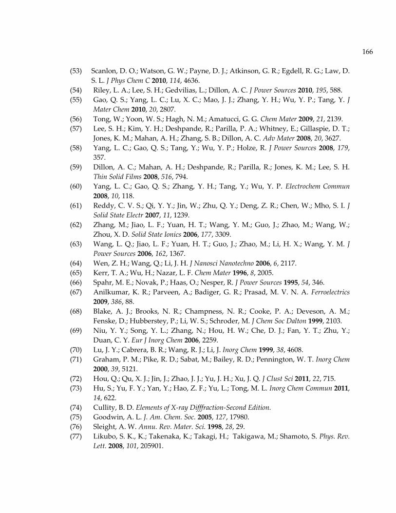
166
(53) Scanlon, D. O.; Watson, G. W.; Payne, D. J.; Atkinson, G. R.; Egdell, R. G.; Law, D.S. L. J Phys Chem C 2010, 114, 4636.
(54) Riley, L. A.; Lee, S. H.; Gedvilias, L.; Dillon, A. C. J Power Sources 2010, 195, 588.(55) Gao, Q. S.; Yang, L. C.; Lu, X. C.; Mao, J. J.; Zhang, Y. H.; Wu, Y. P.; Tang, Y. J
Mater Chem 2010, 20, 2807.(56) Tong, W.; Yoon, W. S.; Hagh, N. M.; Amatucci, G. G. Chem Mater 2009, 21, 2139.(57) Lee, S. H.; Kim, Y. H.; Deshpande, R.; Parilla, P. A.; Whitney, E.; Gillaspie, D. T.;
Jones, K. M.; Mahan, A. H.; Zhang, S. B.; Dillon, A. C. Adv Mater 2008, 20, 3627.(58) Yang, L. C.; Gao, Q. S.; Tang, Y.; Wu, Y. P.; Holze, R. J Power Sources 2008, 179,
357.(59) Dillon, A. C.; Mahan, A. H.; Deshpande, R.; Parilla, R.; Jones, K. M.; Lee, S. H.
Thin Solid Films 2008, 516, 794.(60) Yang, L. C.; Gao, Q. S.; Zhang, Y. H.; Tang, Y.; Wu, Y. P. Electrochem Commun
2008, 10, 118.(61) Reddy, C. V. S.; Qi, Y. Y.; Jin, W.; Zhu, Q. Y.; Deng, Z. R.; Chen, W.; Mho, S. I. J
Solid State Electr 2007, 11, 1239.(62) Zhang, M.; Jiao, L. F.; Yuan, H. T.; Wang, Y. M.; Guo, J.; Zhao, M.; Wang, W.;
Zhou, X. D. Solid State Ionics 2006, 177, 3309.(63) Wang, L. Q.; Jiao, L. F.; Yuan, H. T.; Guo, J.; Zhao, M.; Li, H. X.; Wang, Y. M. J
Power Sources 2006, 162, 1367.(64) Wen, Z. H.; Wang, Q.; Li, J. H. J Nanosci Nanotechno 2006, 6, 2117.(65) Kerr, T. A.; Wu, H.; Nazar, L. F. Chem Mater 1996, 8, 2005.(66) Spahr, M. E.; Novak, P.; Haas, O.; Nesper, R. J Power Sources 1995, 54, 346.(67) Anilkumar, K. R.; Parveen, A.; Badiger, G. R.; Prasad, M. V. N. A. Ferroelectrics
2009, 386, 88.(68) Blake, A. J.; Brooks, N. R.; Champness, N. R.; Cooke, P. A.; Deveson, A. M.;
Fenske, D.; Hubberstey, P.; Li, W. S.; Schroder, M. J Chem Soc Dalton 1999, 2103.(69) Niu, Y. Y.; Song, Y. L.; Zhang, N.; Hou, H. W.; Che, D. J.; Fan, Y. T.; Zhu, Y.;
Duan, C. Y. Eur J Inorg Chem 2006, 2259.(70) Lu, J. Y.; Cabrera, B. R.; Wang, R. J.; Li, J. Inorg Chem 1999, 38, 4608.(71) Graham, P. M.; Pike, R. D.; Sabat, M.; Bailey, R. D.; Pennington, W. T. Inorg Chem
2000, 39, 5121.(72) Hou, Q.; Qu, X. J.; Jin, J.; Zhao, J. J.; Yu, J. H.; Xu, J. Q. J Clust Sci 2011, 22, 715.(73) Hu, S.; Yu, F. Y.; Yan, Y.; Hao, Z. F.; Yu, L.; Tong, M. L. Inorg Chem Commun 2011,
14, 622.(74) Cullity, B. D. Elements of X-ray Difffraction-Second Edition.(75) Goodwin, A. L. J. Am. Chem. Soc. 2005, 127, 17980.(76) Sleight, A. W. Annu. Rev. Mater. Sci. 1998, 28, 29.(77) Likubo, S. K., K.; Takenaka, K.; Takagi, H.; Takigawa, M.; Shamoto, S. Phys. Rev.
Lett. 2008, 101, 205901.

167
(78) Shirane, G. T., A. J. Phys. Soc. Jpn. 1951, 7, 1.(79) Shirane, G. H., S. J. Phys. Soc. Jpn. 1951, 6, 265.(80) Holcombe, C. E. S., D. D. J. Am. Ceram. Soc 1978, 61, 163.(81) Evans, J. S. O. M., T. A.; Vogt, T.; Subramanian, M. A.; Sleight, A. W Chem. Mater.
1996, 8.(82) Mary, T. A. E., J. S. O.; Vogt, T.; Sleight, A. W Science 1996, 272, 90.(83) Lind, C. W., A. P.; Hu, Z. B.; Short, S.; Jorgensen, J. D Chem. Mater. 1998, 10, 2335.(84) Korthuis, V. K., N.; Sleight, A. W.; Roberts, N.; Dupree, R.;Warren, W. W Chem.
Mater. 1995, 7, 412.(85) Evans, J. S. O. M., T. A.; Sleight, A. W J. Solid State Chem 1997, 133, 580.(86) Lightfoot, P. W., D. A.; Maple, M. J.; Villaescusa, L. A.; Wright,P. A J. Mater. Chem.
2001, 11, 212.(87) Williams, D. J. P., D. E.; Lincoln, F. J.; Kouvetakis, J.; O’Keeffe,M J. Solid State
Chem 1997, 134, 164.(88) Benjamin K. Greve, K. L. M., Peter L. Lee, Peter J. Chupas, Karena W. Chapman,
and Angus P. Wilkinson* 2010, 132.(89) Tao, J. Z. S., A. W J. Solid State Chem 2003, 173, 45.(90) Karena W. Chapman, P. J. C., and Cameron J. Kepert J. Am. Chem. Soc. 2005, 127,
15630.(91) Serena Margadonna, K. P., and Andrew N. Fitch J. Am. Chem. Soc. 2004, 126, 15390.(92) Karena W. Chapman, P. J. C., ‡ and Cameron J. Kepert J. Am. Chem. Soc. 2006, 128,
7009.(93) Jayaraman, A. B., E.; Dernier, P. D.; Longinotti, L. D Phys. Rev. Lett. 1973, 31, 700.(94) Arvanitidis, J. P., K.; Margadonna, S.; Prassides, K.; Fitch, A. N Nature 2003, 425,
599.(95) Keller-flaig, R. A., E. Adv. Eng. Mater. 2002, 4.(96) Takenaka, K. T., H. Appl. Phys. Lett. 2009, 94.(97) Salvador, J. R. G., F.; Hogan, T.; Kanatzidis, M. G. Nature 2003, 425, 702.(98) Fluegel, B. Z., Y.; Mascarenhas, A.; Huang, X. Y.; Li, J. Phys. Rev. B 2004, 70.(99) Huang, X. Y. H. I., H. R.; Le, V.; Li, J. Chem. Mater. 2001, 13.(100) Huang, X. Y. L., J.; Fu, H. J. Am. Chem. Soc. 2000, 122.(101) Huang, X. Y. L., J.; Zhang, Y.; Mascarenhas, A. J. Am. Chem. Soc. 2003, 125, 7049.(102) Huang, X. Y. L., J. J. Am. Chem. Soc. 2007, 129.(103) Huang, X. Y. R., M.; Emge, T.J.; Bi, W.; Thiagarajan, S.; Cheng, J.; Yang, R.; and Li,
J. Angew. Chem. Int. Ed. 2009, 48.(104) Y. Zhang, Z. I., Y. Ren, P. A. Parilla, S. P. Ahrenkiel, P. L. Lee, A. Mascarenhas, M.
J. McNevin, I. Naumov,H.-X. Fu, X.-Y. Huang, and J. Li Phys. Rev. Lett. 2007, 99,215901.
(105) Zhang, Y. D., G.M.; Fluegel, B.; Wei, S.H.; Mascarenhas, A.; Huang, X. Y.; Li, J.;Wang, L.W. Phys. Rev. Lett. 2006, 96.

168
(106) Lee, S. H.; Deshpande, R.; Parilla, P. A.; Jones, K. M.; To, B.; Mahan, A. H.; Dillon,A. C. Adv. Mater. 2006, 18, 763.
(107) Xu, Y.; Lu, J. J.; Goh, N. K. J Mater Chem 1999, 9, 1599.(108) Hagrman, P. J.; LaDuca, R. L.; Koo, H. J.; Rarig, R.; Haushalter, R. C.; Whangbo,
M. H.; Zubieta, J. Inorg. Chem. 2000, 39, 4311.(109) Yan, B. B.; Xu, Y.; Goh, N. K.; Chia, L. S. Chem. Commun. 2000, 2169.(110) Fluegel, B.; Zhang, Y.; Mascarenhas, A.; Huang, X.; Li, J. Phys Rev B 2004, 70.(111) Fu, H. X.; Li, J. J. Chem. Phys. 2004, 120, 6721.(112) Waser, R.; Böttger, U.; Tiedke, S. Polar Oxides WILEY-VCH Verlag GmbH & Co.
2005(113) Bergh, A.; Craford, G.; Duggal, A.; Haitz, R. Physics Today 2001, 54, 42.(114) Bowers, M. J.; McBride, J. R.; Rosenthal, S. J. Journal of the American Chemical
Society 2005, 127, 15378.(115) Hines, M. A.; Guyot-Sionnest, P. J Phys Chem B 1998, 102, 3655.(116) Mueller, A. H.; Petruska, M. A.; Achermann, M.; Werder, D. J.; Akhadov, E. A.;
Koleske, D. D.; Hoffbauer, M. A.; Klimov, V. I. Nano Lett 2005, 5, 1039.(117) Nag, A.; Sarma, D. D. J Phys Chem C 2007, 111, 13641.(118) Yang, W. J.; Luo, L. Y.; Chen, T. M.; Wang, N. S. Chem Mater 2005, 17, 3883.(119) Ki, W. L., J. J. Am. Chem. Soc. 2008, 130.(120) Liu, Z. W.; Qayyum, M. F.; Wu, C.; Whited, M. T.; Djurovich, P. I.; Hodgson, K.
O.; Hedman, B.; Solomon, E. I.; Thompson, M. E. Journal of the American ChemicalSociety 2011, 133, 3700.