シリコン鏡面ウェーハの寸法規格に関する 標準仕様20%83v%83%8a...直径(mm)...
TRANSCRIPT

JEIT
シ
(1)
電子情報技術産業協会規格
Standard of Japan Electronic and Information Technology Industries Association
シリコン鏡面ウェーハの寸法規格に関する標準仕様
Standard specification for dimensional properties of silicon wafers with specular surfaces
社団法人 電子情報技術産業協会
Japan Electronic and Information Technology Industries Association
シリコン技術委員会Silicon Technologies Committee
情報処理標準化運営委員会
Managing Committee on Information Technology Standardization
発 行
JEITA EM-3602 (旧 JEIDA-27-1999)
作 成
A半導体部会 シリコン規格管理小委員会の終息に伴い、本規格は2016年3月(平成28年3月)をもって廃止されました。
リコン規格管理小委員会の活動記録として公開するものです。
1976 年 1 月制定
2002 年 7 月改正
2016 年 3 月 廃止

JEITA EM-3602
(1)
目 次
ページ
1. 適用範囲 ・・・・・・・・・・・・・・・・・・・・・・・・・・・・・・・・・・・・・・・・・・・・・・・・・・・・・・・・・・・・・・・・・・・・・・・・・・・・・・・・ 1
2. 規定項目及び標準仕様 ・・・・・・・・・・・・・・・・・・・・・・・・・・・・・・・・・・・・・・・・・・・・・・・・・・・・・・・・・・・・・・・・・・・・ 1
2.1 直径及び厚さ ・・・・・・・・・・・・・・・・・・・・・・・・・・・・・・・・・・・・・・・・・・・・・・・・・・・・・・・・・・・・・・・・・・・・・・・・・・ 1
2.2 フラット ・・・・・・・・・・・・・・・・・・・・・・・・・・・・・・・・・・・・・・・・・・・・・・・・・・・・・・・・・・・・・・・・・・・・・・・・・・・・・・ 1
2.3 ノッチ ・・・・・・・・・・・・・・・・・・・・・・・・・・・・・・・・・・・・・・・・・・・・・・・・・・・・・・・・・・・・・・・・・・・・・・・・・・・・・・・・ 2
2.4 ウェーハ面方位 ・・・・・・・・・・・・・・・・・・・・・・・・・・・・・・・・・・・・・・・・・・・・・・・・・・・・・・・・・・・・・・・・・・・・・・・・ 2
2.5 300mm 径ウェーハ・・・・・・・・・・・・・・・・・・・・・・・・・・・・・・・・・・・・・・・・・・・・・・・・・・・・・・・・・・・・・・・・・・・・・・ 2
シリコン鏡面ウェーハの寸法規格に関する標準仕様の解説 ・・・・・・・・・・・・・・・・・・・・・・・・・・・・・・・・・・・・・・・・ 4

JEITA EM-3602
- - 1
電子情報技術産業協会規格
シリコン鏡面ウェーハの寸法規格に関する標準仕様
Standard specification for dimensional properties of silicon wafers with specular surfaces
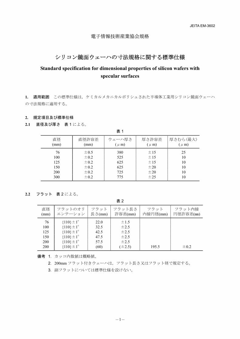
1. 適用範囲 この標準仕様は,ケミカルメカニカルポリシュされた半導体工業用シリコン鏡面ウェーハ
の寸法規格に適用する。
2. 規定項目及び標準仕様
2.1 直径及び厚さ 表 1 による。
表 1
2.2 フラット 表 2 による。
表 2
備考 1. カッコ内数値は概略値。
2. 200mm フラット付きウェーハは,フラット長さ又はフラット径で規定する。
3. 副フラットについては標準仕様を設けない。
直径 (mm)
直径許容差 (mm)
ウェーハ厚さ (μm)
厚さ許容差 (μm)
厚さむら(最大) (μm)
76 ±0.5 380 ±15 25 100 ±0.2 525 ±15 10 125 ±0.2 625 ±15 10 150 ±0.2 625 ±20 10 200 ±0.2 725 ±20 10 300 ±0.2 775 ±25 10
直径(mm)
フラットのオリエンテーション
フラット長さ(mm)
フラット長さ許容差(mm)
フラット 内接円径(mm)
フラット内接円径許容差(㎜)
76 {110}±1° 22.0 ±1.5 100 {110}±1° 32.5 ±2.5 125 {110}±1° 42.5 ±2.5 150 {110}±1° 47.5 ±2.5 200 {110}±1° 57.5 ±2.5 200 {110}±1° (60) (±2.5) 195.5 ±0.2
シリコン鏡面ウェーハの寸法規格に関する標準仕様
JEITA EM-3602
- - 2
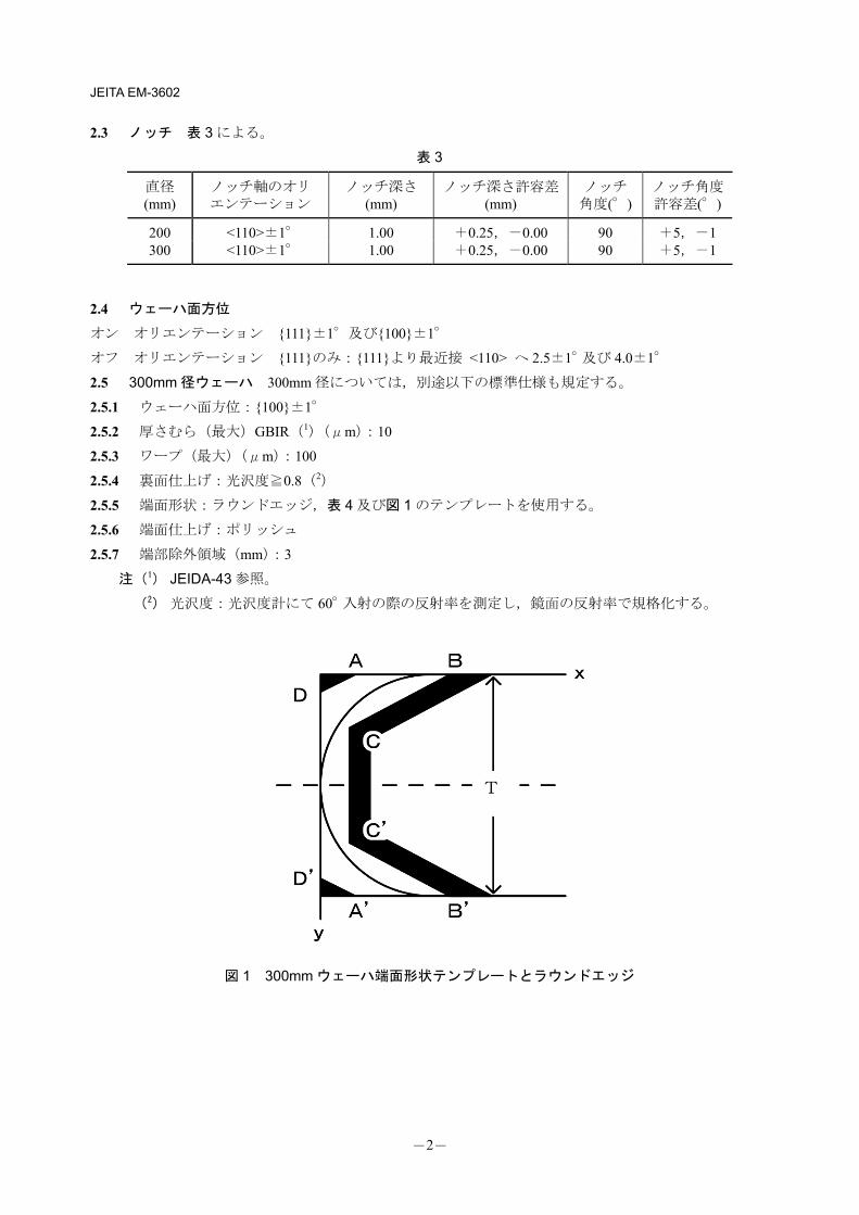
2.3 ノッチ 表 3 による。
表 3
2.4 ウェーハ面方位
オン オリエンテーション {111}±1°及び{100}±1°
オフ オリエンテーション {111}のみ:{111}より最近接 <110> へ 2.5±1°及び 4.0±1°
2.5 300mm 径ウェーハ 300mm 径については,別途以下の標準仕様も規定する。
2.5.1 ウェーハ面方位:{100}±1°
2.5.2 厚さむら(最大)GBIR(1)(μm):10
2.5.3 ワープ(最大)(μm):100
2.5.4 裏面仕上げ:光沢度≧0.8(2)
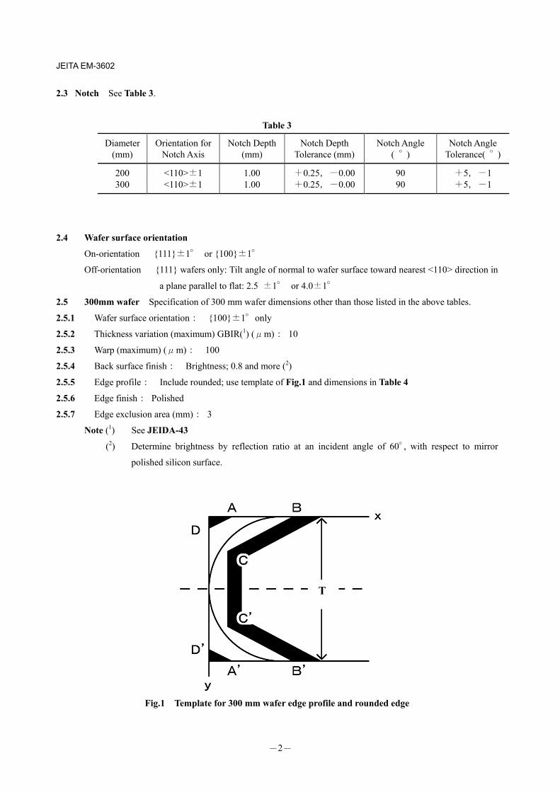
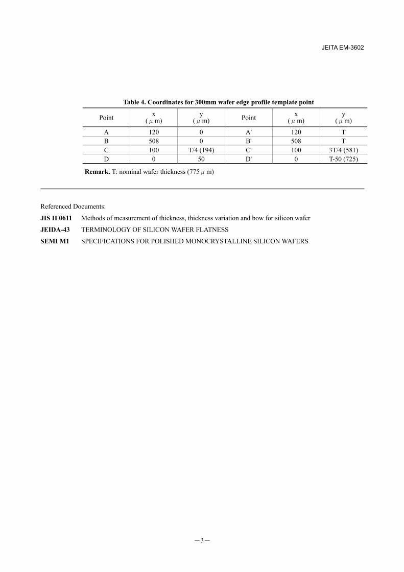
2.5.5 端面形状:ラウンドエッジ,表 4 及び図 1 のテンプレートを使用する。
2.5.6 端面仕上げ:ポリッシュ
2.5.7 端部除外領域(mm):3
注(1) JEIDA-43 参照。
(2) 光沢度:光沢度計にて 60°入射の際の反射率を測定し,鏡面の反射率で規格化する。
図 1 300mm ウェーハ端面形状テンプレートとラウンドエッジ
直径(mm)
ノッチ軸のオリ エンテーション
ノッチ深さ(mm)
ノッチ深さ許容差(mm)
ノッチ 角度(°)
ノッチ角度許容差(°)
200 <110>±1° 1.00 +0.25,-0.00 90 +5,-1 300 <110>±1° 1.00 +0.25,-0.00 90 +5,-1
T
JEITA EM-3602
- - 3
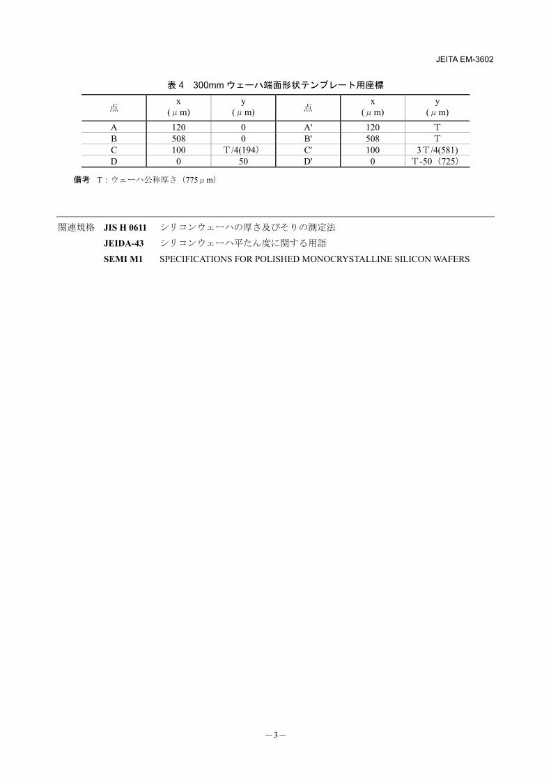
表 4 300mm ウェーハ端面形状テンプレート用座標
備考 T:ウェーハ公称厚さ(775μm)
関連規格 JIS H 0611 シリコンウェーハの厚さ及びそりの測定法
JEIDA-43 シリコンウェーハ平たん度に関する用語
SEMI M1 SPECIFICATIONS FOR POLISHED MONOCRYSTALLINE SILICON WAFERS
点 x
(μm) y
(μm) 点 x
(μm) y
(μm)
A 120 0 A' 120 T B 508 0 B' 508 T C 100 T/4(194) C' 100 3T/4(581) D 0 50 D' 0 T-50(725)
JEITA EM-3602 解説
- - 4
シリコン鏡面ウェーハの寸法規格に関する標準仕様の解説
この解説は,本体及び附属書に記載した事柄,参考に記載した事柄,並びにこれらに関連した事柄を説
明するためのもので,規格の一部ではない。
1. 制定・改正の趣旨及び経緯
1.1 制定の趣旨 ウェーハの寸法規格に関する標準仕様は半導体工業の材料コスト,製品コストの引下
げ,ウェーハの生産・供給の円滑化並びに今後の素子及び各種製造装置開発の円滑化に寄与することを目
的としている。JEIDA-27 は最初 1976 年 1 月に制定された。当時からウェーハ直径は慣習的にインチ寸法
が用いられていたが,これをメートル単位に換算する際に種々の値が用いられたため,寸法規格に関する
標準仕様を作成することとした。このメートル単位(SI)は,直径 100mm 以上の SEMI M1 規格に採用さ
れ,世界標準となった。
1.2 1997 年以降の改正の経緯 ウェーハの寸法規格に関する標準仕様は,ウェーハの大口径化に伴って
逐次改正が行われてきた。1994 年 12 月の東京でのシリコンサミット会議において,次期ウェーハの口径
を 300mm とすることが世界的に合意されたことを受け,(社)日本電子工業振興協会のシリコン技術委員
会は,新たに大口径シリコンウェーハ技術専門委員会を設け 300mm ウェーハの仕様について検討を行っ
た。この結果が当規格の 1997 年の改定で新たに 300mm ウェーハの標準仕様の追加となった。また大口径
シリコンウェーハ技術専門委員会での実験を伴う検討結果基づいて,日本から SEMI M1.15 300mm 規格改
正の提言を行い,世界的な統一標準仕様の確立を目指した。当規格の 1996 年の改正における解説には大口
径シリコンウェーハ技術専門委員会の 1995 年の審議内容を記載し,また 1997 年の改正では 1996 年の審議
内容を増補して記載した。1997 年と 1998 年の審議経過については,別途報告書(99-基-20 大口径シリ
コンウェーハ技術に関する調査研究報告書)が 1999 年 3 月に発行されている(一部英文)。今回の改正で
は,現在使用量が著しく少なくなった直径の仕様,実用に供されなかった直径の仕様を削除すると共に,
規格許容値についてはその後の製造工程能力の向上を加味し,改定を行った。また SEMI 標準との整合性
についても検討を行った。
2. 主な改正点及び補足説明
2.1 1999 年現在使用量が著しく減少した以下の直径の仕様を廃止した。
直径(mm) 40, 50, 60, 90
2.2 実用に供されなかった以下の直径の仕様を廃止した。
直径(mm) 175
2.3 76mm はかなり使用されているため存続させることとし, 寸法仕様については他の径と整合性をと
り, 若干の変更を行ったが SEMI 規格の 3 インチとは一致していない。
2.4 旧表 200mm 以下の項目並びに標準仕様は,表 1 直径及び厚さ,表 2 フラット及び表 3 ノッ
チに分割し,該当する直径の仕様のみ表示することとした。
2.5 SEMI M1 は直径 100mm 及び 125mm の仕様については副フラットのない寸法仕様を採用し,また直
径 150mm の仕様については厚さ 625μm を寸法仕様として採用しているため,当規格も採用した。

JEITA EM-3602 解説
- - 5
2.6 直径 300mm が実用の段階となったため,旧表 300mm 径の項目並びに標準仕様を廃止して,表 1
直径及び厚さ,表 3 ノッチに追加し,表に追加できない 300mm 標準仕様は 2.17 に列挙することとした。
2.7 直径 200mm のフラット長さは 57.5mm となっているが,SEMI M1 は 60mm を採用し,フラット長さ
はなく内接円としていることが審議過程で判明した。しかし直径 200mm ウェーハは今後ノッチ付きが主
流となるため,あえて統一せず併用することとした。
2.8 品質グレードⅠ,Ⅱの区分は製造技術の向上により不要となったため廃止した。
2.9 オフ オリエンテーションは SEMI M1 規格に合わせ 3.0°を廃止した。
2.10 旧規格では面方位は個称となっていたが,実情では総称であり,SEMI 規格も総称となっていたため,
総称に改めることとした。このため旧規格における JEIDA-18 シリコン単結晶の結晶方位の測定法の引
例及び解説が不要となったため削除した。
2.11 300mm 厚さむらの測定位置は,1997 年及び 1998 年の改定増補では,検査装置がないため 9 点測定
となっているが,その後検査装置が実用化されため,JEIDA-43 シリコンウェーハ平たん度に関する用語
に規定される GBIR とし,旧図 3-1 厚さむら測定位置は廃止した。ノッチの測定に用いられた旧図 3-2
ノッチ形状及び旧図 3-4 ノッチに対する原点と座標系は,ASTM F-1152 Standard Test Method for
Dimensions of Notches on Silicon Wafers が用いられるようになったため廃止した。
2.12 旧図 3-2 ノッチに対する原点と座標系及び旧図 3-3 ノッチ形状は,200mm ノッチ付きウェーハが
普及したため廃止した。
2.13 300mm 端面形状については,最初の SEMI 案である Rounded(ラウンドエッジ)を採用したが,そ
の後SEMI側はCMP研磨の際にウェーハの飛び出しが生じるとしてRoundedを排除する規格を制定した。
これについて大口径シリコンウェーハ専門委員会で 3 種類のエッジ形状に対する CMP 研磨実験を行った
結果,差異がないことが証明された(99-基-20 参照)。ラウンドエッジはエッジ全体が連続的であるため
研磨加工が均一に行われ,またエッジを確実につかめるため,日本から最初の SEMI 規格に戻すことを要
求したところ受け入れられ,T/3 と T/4 の二種類のテンプレートが規定された。しかし,この二種類のテ
ンプレートを統合する案を当委員会から提示したところ,この提案も受け入れられた。このような経緯か
ら,SEMI の了解を得て,当規格においても SEMI テンプレートによる端面形状を図 1 300mm ウェーハ
端面形状テンプレートとラウンドエッジ及び表 4 300mm ウェーハ端面形状テンプレート用座標に規定
することとした。
2.14 旧規格表 300mm 径の項目並びに標準仕様 3-18 表裏識別及び図 3-4 表裏識別用レーザマーク
における,表裏識別のためウェーハ表面側にソフトレーザマークを付けると規定した項目は,300mm の
SEMI 規格では全て裏面にハードレーザマークを付けることとなったので,混乱を避けるため廃止した。
JEITA EM-3602 解説
- - 6
3. JEITA EM-3602 審議委員会の構成表
情報処理標準化運営委員会
委 員 長 柴 田 彰 ㈱デンソーウェーブ
シリコン技術委員会
委 員 長 垂 井 康 夫 東京農工大学 幹 事 岡 山 重 夫 産業技術総合研究所
同 金 山 敏 彦 産業技術総合研究所 同 小 山 浩 日本電子㈱
委 員 井 上 直 久 大阪府立大学 同 宮 崎 守 正 三菱住友シリコン㈱ 同 大 橋 弘 通 ㈱東芝 同 福 田 哲 生 富士通㈱ 同 松 本 行 雄 アクセント オプティカル テクノロジーズ㈱ 同 今 井 久 也 旭化成マイクロシステム㈱ 同 辻 村 学 ㈱荏原製作所 同 青 島 孝 明 エム・イー・エム・シー㈱ 同 伊佐治 弘 キヤノン㈱ 同 進 藤 健 一 黒田精工㈱ 同 中 井 康 秀 ㈱コベルコ科研 同 河 野 光 雄 コマツ電子金属㈱ 同 竹 中 卓 夫 信越半導体㈱ 同 島 田 孝 ソニー㈱ 同 藤 野 誠 二 ㈱デンソー 同 宮 下 守 也 ㈱東芝 同 松 下 嘉 明 東芝セラミックス㈱ 同 吉 瀬 正 典 日本エーディーイー㈱ 同 北 野 友 久 日本電気㈱ 同 中 嶋 定 夫 ㈱日本国際電気 同 河 合 直 行 ㈱日立製作所 同 高 崎 金 剛 ㈱富士通研究所 同 吉 住 恵 一 松下電器産業㈱ 同 大 石 博 司 松下電器産業㈱ 同 清 水 保 弘 三菱住友シリコン㈱ 同 益 子 洋 治 三菱電機㈱ 同 秋 山 哲 ㈱レイテックス 同 神 保 丞 ワッカー・エヌエスシーイー㈱
事 務 局 中 瀬 真 (社)電子情報技術産業協会 高 梨 健 一 (社)電子情報技術産業協会

JEITA EM-3602 解説
- - 7
次世代ウェーハ技術専門委員会
委 員 長 福 田 哲 生 富士通㈱ 委 員 辻 村 学 ㈱荏原製作所
同 稲 葉 章 浩 エム・イー・エム・シー㈱ 同 坂 口 清 文 キヤノン㈱ 同 進 藤 健 一 黒田精工㈱ 同 中 井 康 秀 ㈱コベルコ科研 同 三 上 勇 介 コマツ電子金属㈱ 同 北河原 豊 信越半導体㈱ 同 柏 木 章 秀 ソニー㈱ 同 宮 下 守 也 ㈱東芝 同 栗 原 誠 司 東芝セラミックス㈱ 同 吉 瀬 正 典 日本エーディーイー㈱ 同 山 村 清 見 日本電気㈱ 同 松 田 安 司 ㈱日立製作所 同 米 田 健 司 松下電器産業㈱ 同 久 保 圭 司 松下電器産業㈱ 同 清 水 保 弘 三菱住友シリコン㈱ 同 松 川 和 人 三菱電機㈱ 同 秋 山 哲 ㈱レイテックス 同 神 保 丞 ワッカー・エヌエスシーイー㈱
オブザーバ 渡 辺 正 晴 日本エーディーイー㈱ 客 員 服 部 寿 ケーエルエー・テンコール㈱
同 垂 井 康 夫 日本農工大学 同 金 山 敏 彦 産業技術総合研究所 同 河 合 健 一 河合企画
事 務 局 高 梨 健 一 (社)電子情報技術産業協会

Standard of Japan Electronic and Information Technology Industries Association
JEITA EM-3602 (JEIDA-27-1999)
Standard specification for dimensional properties of
silicon wafers with specular surfaces
Established in January, 1976 Revised in July, 2002
Prepared by
Silicon Technologies Committee
Managing Committee on Information Technology Standardization
Published by
Japan Electronics and Information Technology Industries Association
11, Kanda-Surugadai 3-shome, Chiyoda-ku, Tokyo 101-0062, Japan Printed in Japan

the original standard in Japanese is to be evidence.
JEITA standards are established independently to any existing patents
on the products, materials or processes they cover.
JEITA assumes absolutely no responsibility toward parties applying
these standards or toward patent owners.
○C 2002 by the Japan Electronics and Information Technology Industries Association
All rights reserved. No part of this standard may be reproduced
in any form or by any means without prior permission in writing
from the publisher.
JEITA EM-3602
( ) 1
Contents
1. Scope ・・・・・・・・・・・・・・・・・・・・・・・・・・・・・・・・・・・・・・・・・・・・・・・・・・・・・・・・・・・・・・・・・・・・・・・・・・・・・・・・・・・・1
2. Item and standard specification ・・・・・・・・・・・・・・・・・・・・・・・・・・・・・・・・・・・・・・・・・・・・・・・・・・・・・・・・・・・・・・・・1 2.1 Diameter and thickness・・・・・・・・・・・・・・・・・・・・・・・・・・・・・・・・・・・・・・・・・・・・・・・・・・・・・・・・・・・・・・・・・・・・・1
2.2 Flat ・・・・・・・・・・・・・・・・・・・・・・・・・・・・・・・・・・・・・・・・・・・・・・・・・・・・・・・・・・・・・・・・・・・・・・・・・・・・・・・・・・・・1
2.3 Notch ・・・・・・・・・・・・・・・・・・・・・・・・・・・・・・・・・・・・・・・・・・・・・・・・・・・・・・・・・・・・・・・・・・・・・・・・・・・・・・・・・・2
2.4 Wafer surface orientation ・・・・・・・・・・・・・・・・・・・・・・・・・・・・・・・・・・・・・・・・・・・・・・・・・・・・・・・・・・・・・・・・・・・2
2.5 300mm wafer ・・・・・・・・・・・・・・・・・・・・・・・・・・・・・・・・・・・・・・・・・・・・・・・・・・・・・・・・・・・・・・・・・・・・・・・・・・・・2
Explanation for Standard specification for dimensional properties of silicon wafers with specular surfaces ・・・・・・・・・4


JEITA EM-3602
- - 1
Standard of Japan Electronics and Information Technology Industries Association
Standard specification for dimensional properties of silicon wafers with specular surfaces
1. Scope This standard specifies standard dimensions for chem-mechanically polished semiconductor silicon
polished wafers.
2. Item and standard specification
2.1 Diameter and thickness See Table 1.
Table 1
2.2 Flat See Table 2.
Table 2
Remark 1. Figures in parentheses are approximate values.
2. For flatted 200 mm wafers the flat should be specified either by flat length or by flat diameter.
3. This specification does not include a specification for secondary flats.
Diameter (mm)
Diameter Tolerance (mm)
Thickness (μm)
Thickness Tolerance (μm)
Total Thickness Variation
(maximum)(μm)
76 ±0.5 380 ±15 25 100 ±0.2 525 ±15 10 125 ±0.2 625 ±15 10 150 ±0.2 625 ±20 10 200 ±0.2 725 ±20 10 300 ±0.2 775 ±25 10
Diameter (mm) Flat Orientation Flat Length
(mm) Flat Length
Tolerance (mm) Flat Diameter
(mm) Flat Diameter
Tolerance (mm)
76 {110}±1° 22.0 ±1.5 100 {110}±1° 32.5 ±2.5 125 {110}±1° 42.5 ±2.5 150 {110}±1° 47.5 ±2.5 200 {110}±1° 57.5 ±2.5 200 {110}±1° (60) (±2.5) 195.5 ±0.2
JEITA EM-3602
- - 2
2.3 Notch See Table 3.
Table 3
2.4 Wafer surface orientation
On-orientation {111}±1° or {100}±1°
Off-orientation {111} wafers only: Tilt angle of normal to wafer surface toward nearest <110> direction in
a plane parallel to flat: 2.5 ±1° or 4.0±1°
2.5 300mm wafer Specification of 300 mm wafer dimensions other than those listed in the above tables.
2.5.1 Wafer surface orientation: {100}±1°only
2.5.2 Thickness variation (maximum) GBIR(1) (μm): 10
2.5.3 Warp (maximum) (μm): 100
2.5.4 Back surface finish: Brightness; 0.8 and more (2)
2.5.5 Edge profile: Include rounded; use template of Fig.1 and dimensions in Table 4
2.5.6 Edge finish: Polished
2.5.7 Edge exclusion area (mm): 3
Note (1) See JEIDA-43
(2) Determine brightness by reflection ratio at an incident angle of 60°, with respect to mirror
polished silicon surface.
Fig.1 Template for 300 mm wafer edge profile and rounded edge
Diameter (mm)
Orientation for Notch Axis
Notch Depth(mm)
Notch Depth Tolerance (mm)
Notch Angle ( °)
Notch Angle Tolerance( °)
200 <110>±1 1.00 +0.25,-0.00 90 +5,-1 300 <110>±1 1.00 +0.25,-0.00 90 +5,-1
T
JEITA EM-3602
- - 3
Table 4. Coordinates for 300mm wafer edge profile template point
Remark. T: nominal wafer thickness (775μm)
Referenced Documents:
JIS H 0611 Methods of measurement of thickness, thickness variation and bow for silicon wafer
JEIDA-43 TERMINOLOGY OF SILICON WAFER FLATNESS
SEMI M1 SPECIFICATIONS FOR POLISHED MONOCRYSTALLINE SILICON WAFERS
Point x (μm)
y (μm) Point x
(μm) y
(μm)
A 120 0 A' 120 T B 508 0 B' 508 T C 100 T/4 (194) C' 100 3T/4 (581) D 0 50 D' 0 T-50 (725)

JEITA EM-3602 Explanation
- - 4
Explanation for Standard specification for dimensional properties of silicon wafers with specular surfaces
The following description have been compiled to describe the matters provided in the standard proper and their
associated matters, and is not part the standard.
1. Purpose and progress of establishment/revision
1.1 Purpose of establishment
The object of wafer standardization is to contribute reduction of material cost and product cost, to economize
production and supply of wafer, and to develop semiconductor and its various semiconductor production
equipments. JEIDA 27 was first established on January 1976. The main purpose was to unify wafer dimensions
in the metric system. At that time, inch measurements were commonly used for wafer dimensions, and various
factors were used to convert to metric measurements. For wafers 100 mm in diameter and larger, metric (SI)
units have been adopted in SEMI Specifications M1 and have become the worldwide standard.
1.2 Progress of revision since 1997
Since its establishment, JEIDA 27 has been revised several times because of the introduction of larger
diameter wafers. The present revision has been made mainly in the form of specifications for wafers 200 mm
and less in diameter. In December 1994, the diameter of the next generation wafer was globally determined to
be 300 mm at a Silicon Summit Conference in Tokyo. At this time, the Silicon Committee of the Japan
Electronic Development Association (JEIDA) organized a Larger Wafer Technical Committee to study
specification of 300 mm silicon wafers. The results were used for the 1997 revision of this standard to add the
300mm standard specification. In addition, the Committee made proposals with the results of the studies
including experiments to the SEMI Standards Silicon Wafer Committee for the revision of its 300 mm wafer
specification (SEMI M1.15) so that a unified worldwide specification could be developed.
The appendix of JEIDA 1996 Revision consisted of progress reports of the 1995 studies and of Committee
and JEIDA 1997 Revision consisted of progress reports of the 1995 and 1996 studies and discussions. The
progress report of 1997 and 1998 was published by JEIDA in March 1999 under the title "Progress Report on
Larger Wafer Technology" (partly English). The present revision has been made the items of 300mm which
now practical use has begun, discontinuation of wafer diameters which show remarkable reduction of use,
abolition of wafer diameter not practical use, and change of tolerances owing to the development of wafer
manufacturing. And also matching to SEMI Standard has been done.
2. Content of present revision and supplemental explanation
2.1 Discontinuation of specifications for the following wafer diameters because remarkable reduction of use in
1999: 40, 50, 60, and 90 mm.
2.2 Abolition of specifications for the following wafer diameter because it is not of practical use: 175 mm.
2.3 Specifications for 76 mm wafers are continued because considerable usage still exists, but some
modifications were made in order to match other wafer diameters in this Specification, but it does not conform
with the 3 inch wafer specification of SEMI M1.
2.4 The table of previous edition "Standard Specification for Diameter less than 200 mm" was reorganized to

JEITA EM-3602 Explanation
- - 5
three tables with only applicable wafer diameters.
2.5 SEMI M1 includes the JEIDA 27 specifications for 100 mm wafers (525μm thickness) without secondary
flat (SEMI M1.11), for 125 mm wafers without secondary flat (SEMI M1.12), and for 150 mm wafers (625μm
thickness) without secondary flat. The SEMI specification for notched 200 mm wafers (SEMI M1.9) is virtually
the same as that in this Specification.
2.6 Specifications for the diameter and thickness of 300 mm wafers are included in Table 1, and notch
specifications are included in Table 3. Items that could not be included in the tables are listed in 2.1.
2.7 The flat length for 200 mm diameter wafers is specified as 57.5 mm, but we found during the discussion that
the flat length in SEMI M1, which specifies flat diameter instead of flat length, is approximately 60 mm. But
JEIDA 27 has not been modified to conform with this requirement because 200 mm notched wafer will be more
common.
2.8 Former quality gradesⅠandⅡwere discontinued because they are no longer necessary because of the
development of wafer manufacturing technology.
2.9 Off-orientation 3.0°has been discontinued in accordance with SEMI M1.
2.10 Crystal surface orientations, previously listed individually, are actually generic and so they are listed in one
place for all diameters in this revision. In this revision, reference to JEIDA 18 "Standard Methods for
Determining the Orientation of a Semiconductor Single Crystal" and its explanation figure have been removed.
2.11 Thickness variation of 300 mm wafers had been previously specified as a 9-point measurement, but since
whole-wafer scanning measurement equipment has become practical for 300 mm wafers, GBIR as specified in
JEIDA 43 "Terminology of Silicon Wafer Flatness" has been adopted, and former Figure 3-1
"Measurement positions of thickness variation" has been removed.
2.12 Former Figure 3-2 "Notch Figure" and former Figure 3-3 "Origin and Coordinate of Notch" were
discontinued because ASTM F-1152 Standard Test Method for Dimensions of Notches on Silicon Wafers
was now widely applied.
2.13 SEMI at first modified the edge profile template for 300 mm wafers, this new template precluded the use of a
rounded profile. However, The Larger Wafer Technical Committee tested 3 kinds of edge profile and proved no
difference between edge profiles with respect to gripping trouble during CMP processing (see JEIDA Report
99-Basic-20). As a rounded edge shape has a continuous profile around the entire wafer edge, it is easy to polish
the edge uniformly and also to secure the wafer more firmly with edge gripping. Consequently the Committee
requested SEMI to modify the template to permit the rounded profile shape. The SEMI Silicon Wafer
Committee accepted and two templates T/3 and T/4 were listed. The Committee again requested to modify the
new template to unify 2 templates, and SEMI Silicon Wafer Committee accepted this recommendation and was
adopted in a revision to the SEMI 300 mm wafer specification (SEMI M1.15). This revision of JEIDA 27 has
adopted and specified the same template, with the permission of SEMI, as Figure 1, "Template for 300 mm
Wafer Edge Profile and Rounded Edge" and Table 4 "Coordinates for 300 mm Wafer Edge Profile
Template and Rounded Edge".
2.14 The previous specification 3-18 "Discrimination of front surface and back surface" and Figure 3-4
"Laser mark for discrimination of front and back surface", which had specified a soft laser mark on front
surface of 300 mm wafers were removed to prevent confusion because a hard laser mark on the back surface of
all 300 mm wafers is specified in SEMI M1.15.

JEITA EM-3602 Explanation
- - 6
3. Committee member
Managing Committee on Information Technology Standardization
Chairman Akira Shibata DENSO WAVE INCORPORATED
Silicon Technologies Committee
Chairman Yasuo Tarui Tokyo University of Agriculture and Technology Co-Chairman Shigeo Okayama National Institute of Advanced Industrial Science and Technology Co-Chairman Toshihiko Kanayama National Institute of Advanced Industrial Science and Technology Co-Chairman Hiroshi Koyama JEOL Ltd. Member Naohisa Inoue Osaka Prefecture University Member Morimasa Miyazaki SUMITOMO MITSUBISHI SILICON CORPORATION Member Hiromichi Ohashi Toshiba Corp. Member Tetsuo Fukuda FUJITSU LIMITED Member Yukio Matsumoto Accent Optical Technologies Co., Ltd. Member Hisaya Imai Asahi Kasei Microsystems Co., Ltd. Member Manabu Tsujimura Ebara Corporation Member Takaaki Aoshima MEMC Japan Ltd. Member Hiroshi Isaji Canan Inc. Member Kenichi Shindo KURODA Precision Industries Ltd. Member Yasuhide Nakai Kobelco Research Institute, Inc. Member Mitsuo Kohno Komatsu Electronic Metals Co., Ltd. Member Takuo Takenaka Shin-Etsu Handotai Co., Ltd. Member Takashi Shimada Sony Corp. Member Seiji Fujino DENSO CORPORATION Member Moriya Miyashita Toshiba Corp. Member Yoshiaki Matsushita Toshiba Ceramics Co., Ltd. Member Masanori Yoshise JAPAN ADE LTD. Member Tomohisa Kitano NEC Corp. Member Sadao Nakajima Hitachi Kokusai Electric Inc. Member Naoyuki Kawai Hitachi, Ltd. Member Kaneta Takasaki Fujitsu Laboratories Ltd. Member Keiichi Yoshizumi Matsushita Electric Industrial Co., Ltd. Member Hiroshi Ohishi Matsushita Electric Industrial Co., Ltd. Member Yasuhiro shimizu SUMITOMO MITSUBISHI SILICON CORPORATION Member Yoji Mashiko Mitsubishi Electric Corp. Member Satoshi Akiyama RAYTEX CORPORATION Member Susumu Jinbo Wacker NSCE Corp. Secretariat Makoto Nakase Japan Electronics and Information Technology Industries Association Secretariat Kenichi Takanashi Japan Electronics and Information Technology Industries Association

JEITA EM-3602 Explanation
- - 7
Next-Generation Wafer Technologies Subcommittee
Chairman Tetsuo Fukuda FUJITSU LIMITED
Member Manabu Tsujimura Ebara Corporation
Member Akihiro Inaba MEMC Japan Ltd.
Member Kiyofumi Sakaguchi Canan Inc.
Member Kenichi Shindo KURODA Precision Industries Ltd.
Member Yasuhide Nakai Kobelco Research Institute, Inc.
Member Yusuke Mikami Komatsu Electronic Metals Co., Ltd.
Member Yutaka Kitagawara Shin-Etsu Handotai Co., Ltd.
Member Akihide Kashiwagi Sony Corp.
Member Moriya Miyashita Toshiba Corp.
Member Seiji Kurihara Toshiba Ceramics Co., Ltd.
Member Masanori Yoshise JAPAN ADE LTD.
Member Kiyomi Yamamura NEC Corp.
Member Yasushi Matsuda Hitachi, Ltd.
Member Kenji Yoneda Matsushita Electric Industrial Co., Ltd.
Member Keiji Kubo Matsushita Electric Industrial Co., Ltd.
Member Yasuhiro shimizu SUMITOMO MITSUBISHI SILICON CORPORATION
Member Kazuhito Matsukawa Mitsubishi Electric Corp.
Member Satoshi Akiyama RAYTEX CORPORATION
Member Susumu Jinbo Wacker NSCE Corp.
Observer Masaharu Watanabe JAPAN ADE LTD.
Guest Member Hisashi Hattori KLA-Tencor Japan
Guest Member Yasuo Tarui Tokyo University of Agriculture and Technology
Guest Member Toshihiko Kanayama National Institute of Advanced Industrial Science and Technology
Guest Member Kenichi Kawai Kawai Standard Consulting
Secretariat Kenichi Takanashi Japan Electronics and Information Technology Industries Association


(社)電子情報技術産業協会が発行している規格類は,工業所有権(特許,実
用新案など)に関する抵触の有無に関係なく制定されています。
(社)電子情報技術産業協会は,この規格類の内容に関する工業所有権に対し
て,一切の責任を負いません。
J E I T A E M - 3 6 0 2 2002年7月発行
発 行 (社)電子情報技術産業協会 標準・技術部
〒101-0062 東京都千代田区神田駿河台 3-11
TEL 03-3518-6434 FAX 03-3295-8727
印 刷 (有)ウイード
〒162-0041 東京都新宿区早稲田鶴巻町 556
TEL 03-3513-5751 FAX 03-3513-5752
禁 無 断 転 載
この規格類の全部又は一部を転載しようとする場合
は,発行者の許可を得て下さい。