insidepater.web.cip.com.br/si2016/textos/pdfs/stokes/insidethemachinech... · chapter 10: the g5:...
TRANSCRIPT

Insidethe MachineAn Illustrated Introduction to Microprocessors and Computer Architecture
Jon Stokes
NO STARCH PRESS
San Francisco

INSIDE THE MACHINE. Copyright © 2007 byjon Stokes.
All rights reserved. No part of this work may be reproduced or transmitted in any form or by any means, electronic or mechanical, including photocopying, recording, or by any information storage or retrieval system, without the prior written permission of the copyright owner and the publisher.
Printed in Canada
10 09 08 07 2 3 4 5 6 78 9
ISBN-10: 1-59327-104-2 ISBN-13: 978-1-59327-104-6
Publisher: William Pollock Production Editor: Elizabeth Campbell Cover Design: Octopod Studios Developmental Editor: William Pollock Copyeditors: Sarah Lemaire, Megan Dunchak Compositor: Riley Hoffman Proofreader: Stephanie Provines Indexer: Nancy Guenther
For information on book distributors or translations, please contact No Starch Press, Inc. directly:
No Starch Press, Inc.555 De Haro Street, Suite 250, San Francisco, CA 94107phone: 415.863.9900; fax: 415.863.9950; [email protected]; www.nostarch.com
Library of Congress Cataloging-in-Publication Data
Stokes, DonInside the machine : an illustrated introduction to microprocessors and computer architecture / Don
Stokes.p. cm.
Includes index.ISBN-13: 978-1-59327-104-6 ISBN-10: 1-59327-104-2
l. Computer architecture. 2. Microprocessors--Design and construction. I. Title.TK7895.M5S76 2006 621.39'2--dc22
2005037262
No Starch Press and the No Starch Press logo are registered trademarks of No Starch Press, Inc. Other product and company names mentioned herein may be the trademarks of their respective owners. Rather than use a trademark symbol with every occurrence of a trademarked name, we are using the names only in an editorial fashion and to the benefit of the trademark owner, with no intention of infringement of the trademark.
The information in this book is distributed on an “As Is” basis, without warranty. While every precaution has been taken in the preparation of this work, neither the author nor No Starch Press, Inc. shall have any liability to any person or entity with respect to any loss or damage caused or alleged to be caused direcdy or indirecdy by the informadon contained in it.
The photograph in the center of the cover shows a small portion of an Intel 80486DX2 microprocessor die at 200x optical magnification. Most of the visible features are the top metal interconnect layers which wire most of the on-die components together.
Cover photo by Matt Britt and Matt Gibbs.

To my parents, who instilled in me a love of learning and education, and to my grandparents, who footed the bill.

B R I E F C O N T E N T S
Preface.........................................................................................................................................................................................xv
Acknowledgments............................................................................................................................................................. xvii
Introduction.............................................................................................................................................................................. xix
Chapter 1: Basic Computing Concepts..................................................................................................................... 1
Chapter 2: The Mechanics of Program Execution............................................................................................ 19
Chapter 3: Pipelined Execution................................................................................................................................... 35
Chapter 4: Superscalar Execution...............................................................................................................................61
Chapter 5: The Intel Pentium and Pentium Pro.................................................................................................... 79
Chapter 6: PowerPC Processors: 600 Series, 700 Series, and 7 4 0 0 ................................................ 11 1
Chapter 7: Intel's Pentium 4 vs. Motorola's G4e: Approaches and Design Philosophies.......... 137
Chapter 8: Intel's Pentium 4 vs. Motorola's G4e: The Back End ........................................................... 161
Chapter 9: 64-Bit Computing and x86-64......................................................................................................... 179
Chapter 10: The G 5: IBM's PowerPC 9 7 0 ....................................................................................................... 193
Chapter 1 1: Understanding Caching and Performance................................................................................. 215
Chapter 12: Intel's Pentium M, Core Duo, and Core 2 Duo....................................................................235
Bibliography and Suggested Reading.................................................................................................................... 271
Index 275

C O N T E N T S I N D E T A I L
PREFACE xv
ACKNOWLEDGMENTS xvii
INTRODUCTION x ix
1BASIC COMPUTING CONCEPTS 1The Calculator Model of Computing ....................................................................................................................2The File-Clerk Model of Computing .......................................................................................................................3
The Stored-Program Computer ............................................................................................................ 4Refining the File-Clerk Model ............................................................................................................... 6
The Register File ...............................................................................................................................................................7RAM: When Registers Alone Won't Cut It ..................................................................................................... 8
The File-Clerk Model Revisited and Expanded ..........................................................................9An Example: Adding Two Numbers............................................................................................ 10
A Closer Look at the Code Stream: The Program ..................................................................................... 11General Instruction Types .................................................................................................................. 11The DLW-1 's Basic Architecture and Arithmetic Instruction Format............................. 12
A Closer Look at Memory Accesses: Register vs. Immediate .............................................................. 14Immediate Values ................................................................................................................................... 14Register-Relative Addressing ............................................................................................................ 16
2THE MECHANICS OF PROGRAM EXECUTION 19Opcodes and Machine Language ................................................................................................................... 19
Machine Language on the DLW-1 ................................................................................................. 20Binary Encoding of Arithmetic Instructions .................................................................................21Binary Encoding of Memory Access Instructions ..................................................................23Translating an Example Program into Machine Language.............................................. 25
The Programming Model and the ISA ..............................................................................................................26The Programming Model ..................................................................................................................... 26The Instruction Register and Program Counter .........................................................................26The Instruction Fetch: Loading the Instruction Register ..........................................................28Running a Simple Program: The Fetch-Execute Loop .............................................................28
The C lo c k ..........................................................................................................................................................................29Branch Instructions....................................................................................................................................................... 30
Unconditional Branch ............................................................................................................................30Conditional Branch ................................................................................................................................ 30
Excursus: Booting Up ................................................................................................................................................. 34

3PIPELINED EXECUTION 35The Lifecycle of an Instruction ................................................................................................................................ 36Basic Instruction F lo w ................................................................................................................................................. 38Pipelining Explained ...................................................................................................................................................40Applying the Analogy................................................................................................................................................43
A Non-Pipelined Processor .................................................................................................................43A Pipelined Processor ............................................................................................................................45The Speedup from Pipelining ........................................................................................................ 48Program Execution Time and Completion Rate ..................................................................... 51The Relationship Between Completion Rate and Program Execution Time ............ 52Instruction Throughput and Pipeline Stalls .................................................................................. 53Instruction Latency and Pipeline Stalls ............................................................................................57Limits to Pipelining ................................................................................................................................... 58
4SUPERSCALAR EXECUTION 61Superscalar Computing and IPC .........................................................................................................................64Expanding Superscalar Processing with Execution Units ....................................................................... 65
Basic Number Formats and Computer Arithmetic...................................................................66Arithmetic Logic Units ............................................................................................................................67Memory-Access Units ............................................................................................................................. 69
Microarchitecture and the IS A ...............................................................................................................................69A Brief History of the ISA ....................................................................................................................71Moving Complexity from Hardware to Software.................................................................... 73
Challenges to Pipelining and Superscalar Design ..................................................................................... 74Data Hazards .............................................................................................................................................74Structural H azards....................................................................................................................................76The Register File .......................................................................................................................................77Control Hazards .......................................................................................................................................78
5THE INTEL PENTIUM AND PENTIUM PRO 79The Original Pentium ................................................................................................................................................. 80
Caches ...........................................................................................................................................................81The Pentium's Pipeline............................................................................................................................82The Branch Unit and Branch Prediction .......................................................................................85The Pentium's Back End .........................................................................................................................87x86 Overhead on the Pentium ......................................................................................................... 91Summary: The Pentium in Historical Context ..........................................................................92
The Intel P6 Microarchitecture: The Pentium P ro ..........................................................................................93Decoupling the Front End from the Back End ..........................................................................94The P6 Pipeline .................................................................................................................................... 100Branch Prediction on the P6 .......................................................................................................... 102The P6 Back End ................................................................................................................................. 102CISC, RISC, and Instruction Set Translation .......................................................................... 103The P6 Microarchitecture's Instruction Decoding Unit .................................................... 106The Cost of x86 Legacy Support on the P6 .......................................................................... 107Summary: The P6 Microarchitecture in Historical Context ........................................... 107
Conclusion .................................................................................................................................................................. 1 10
X C o n le n l s in Derail

POWERPC PROCESSORS: 600 SERIES,700 SERIES, AND 7400 1 1 1A Brief History of PowerPC ................................................................................................................................ 112The PowerPC 601 .................................................................................................................................................. 112
The 601 '$ Pipeline and Front End .............................................................................................. 11 3The 601 's Back End ......................................................................................................................... 115Latency and Throughput Revisited .............................................................................................. 117Summary: The 601 in Historical Context .............................................................................. 118
The PowerPC 603 and 603e ........................................................................................................................... 118The 603e's Back End ........................................................................................................................ 119The 603e's Front End, Instruction Window, and Branch Prediction ....................... 122Summary: The 603 and 603e in Historical Context ....................................................... 122
The PowerPC 604 .................................................................................................................................................. 123The 604's Pipeline and Back End .............................................................................................. 123The 604's Front End and Instruction Window .................................................................... 126Summary: The 604 in Historical Context .............................................................................. 129
The PowerPC 604e ............................................................................................................................................... 129The PowerPC 750 (aka the G3) ..................................................................................................................... 129
The 750's Front End, Instruction Window, and Branch Instruction .......................... 130Summary: The PowerPC 750 in Historical Context.......................................................... 132
The PowerPC 7400 (aka the G4) .................................................................................................................. 133The G4's Vector Unit ...................................................................................................................... 135Summary: The PowerPC G4 in Historical Context ............................................................ 135
Conclusion .................................................................................................................................................................. 135
6
7INTEL'S PENTIUM 4 VS. MOTOROLA'S G4E:APPROACHES AND DESIGN PHILOSOPHIES 137The Pentium 4's Speed Addiction .................................................................................................................. 138The General Approaches and Design Philosophies of the Pentium 4 and G4e .................. 141An Overview of the G4e's Architecture and Pipeline ....................................................................... 144
Stages 1 and 2: Instruction Fetch................................................................................................ 145Stage 3: Decode/Dispatch ............................................................................................................ 145Stage 4: Issue ....................................................................................................................................... 146Stage 5: Execute ................................................................................................................................. 146Stages 6 and 7: Complete and Write-Back.......................................................................... 147
Branch Prediction on the G4e and Pentium 4 ......................................................................................... 147An Overview of the Pentium 4's Architecture ......................................................................................... 148
Expanding the Instruction Window ........................................................................................... 149The Trace Cache ................................................................................................................................. 149
An Overview of the Pentium 4's Pipeline .................................................................................................. 155Stages 1 and 2: Trace Cache Next Instruction Pointer................................................... 155Stages 3 and 4: Trace Cache Fetch ......................................................................................... 155Stage 5: Drive ...................................................................................................................................... 155Stages 6 Through 8: Allocate and Rename (ROB) ........................................................... 155Stage 9: Queue ................................................................................................................................. 156Stages 10 Through 12: Schedule .............................................................................................. 156Stages 13 and 14: Issue ............................................................................................................... 157
Con\enfs in Detail XI

Stages 15 and 16: Register Files .............................................................................................. 158Stage 17: Execute .............................................................................................................................. 158Stage 1 8: Flags ................................................................................................................................. 158Stage 19: Branch Check ............................................................................................................... 158Stage 20: Drive ................................................................................................................................. 158Stages 21 and Onward: Complete and Commit .............................................................. 158
The Pentium 4's Instruction Window ............................................................................................................ 159
8INTEL'S PENTIUM 4 VS. M OTOROLA'S G4E:THE BACK END 161Some Remarks About Operand Formats .................................................................................................. 161The Integer Execution Units ................................................................................................................................ 163
The G4e's lUs: Making the Common Case Fast................................................................. 163The Pentium 4's lUs: Make the Common Case Twice as Fast..................................... 164
The Floating-Point Units (FPUs) .......................................................................................................................... 165The G4e's FPU ...................................................................................................................................... 166The Pentium 4's FPU ........................................................................................................................ 167Concluding Remarks on the G4e's and Pentium 4's FPUs ........................................... 168
The Vector Execution Units ................................................................................................................................ 168A Brief Overview of Vector Computing ................................................................................. 168Vectors Revisited: The AltiVec Instruction Set ....................................................................... 169AltiVec Vector Operations ............................................................................................................. 170The G4e's VU: SIMD Done Right .............................................................................................. 173Intel's MMX ............................................................................................................................................ 174SSE and SSE2 ...................................................................................................................................... 175The Pentium 4's Vector Unit: Alphabet Soup Done Quickly ....................................... 176Increasing Floating-Point Performance with SSE2 ............................................................ 177
Conclusions ................................................................................................................................................................ 177
964-BIT COMPUTING AND X 8 6 -6 4 179Intel's IA-64 and AMD's x86-64 ..................................................................................................................... 180Why 64 Bits? ........................................................................................................................................................... 181What Is 64-Bit Computing?................................................................................................................................ 1 81Current 64-Bit Applications ................................................................................................................................ 183
Dynamic Range ................................................................................................................................... 183The Benefits of Increased Dynamic Range, or,
How the Existing 64-Bit Computing Market Uses 64-Bit Integers.................... 184Virtual Address Space vs. Physical Address Space ........................................................... 1 85The Benefits of a 64-Bit Address ................................................................................................. 186
The 64-Bit Alternative: x86-64 ................................................................................................................. 187Extended Registers ............................................................................................................................. 187More Registers ...................................................................................................................................... 188Switching Modes ................................................................................................................................ 189Out with the Old ................................................................................................................................. 192
Conclusion ................................................................................................................................................................. 192
XII c onlenfs in Deta i l

THE G 5 : IBM'S POWERPC 970 193Overview: Design Philosophy .......................................................................................................................... 194Caches and Front End ......................................................................................................................................... 194Branch Prediction .................................................................................................................................................... 195The Trade-Off: Decode, Cracking, and Group Formation ............................................................... 196
The 970's Dispatch Rules ............................................................................................................... 198Predecoding and Group Dispatch ............................................................................................ 199Some Preliminary Conclusions on the 970's Group Dispatch Scheme ................. 199
The PowerPC 970's Back End ............................................................................................................................200Integer Unit, Condition Register Unit, and Branch Unit ................................................. 201The Integer Units Are Not Fully Symmetric ............................................................................201Integer Unit Latencies and Throughput ..................................................................................... 202TheCRU .................................................................................................................................................... 202Preliminary Conclusions About the 970's Integer Performance .................................. 203
Load-Store Units.......................................................................................................................................................... 203Front-Side Bus ............................................................................................................................................................204The Floating-Point Units ......................................................................................................................................... 205Vector Computing on the PowerPC 970 ...................................................................................................... 206Floating-Point Issue Queues ................................................................................................................................ 209
Integer and Load-Store Issue Queues ........................................................................................ 210BU and CRU Issue Queues ..............................................................................................................210Vector Issue Queues ............................................................................................................................211
The Performance Implications of the 970's Group Dispatch Scheme .......................................... 211Conclusions ..................................................................................................................................................................213
1 1UNDERSTANDING CACHING AND PERFORMANCE 215Caching Basics .......................................................................................................................................................... 215
The Level 1 Cache ................................................................................................................................ 217The Level 2 Cache ................................................................................................................................ 218Example: A Byte's Brief Journey Through the Memory Hierarchy ..............................218Cache Misses ......................................................................................................................................... 219
Locality of Reference ................................................................................................................................................220Spatial Locality of Data ..................................................................................................................... 220Spatial Locality of Code ....................................................................................................................221Temporal Locality of Code and Data ........................................................................................ 222Locality: Conclusions ..........................................................................................................................222
Cache Organization: Blocks and Block Frames .......................................................................................223Tag RAM .......................................................................................................................................................................224Fully Associative Mapping ................................................................................................................................... 224Direct Mapping .......................................................................................................................................................... 225N-Way Set Associative Mapping ....................................................................................................................226
Four-Way Set Associative Mapping ........................................................................................... 226Two-Way Set Associative Mapping ........................................................................................... 228Two-Way vs. Direct-Mapped ......................................................................................................... 229Two-Way vs. Four-Way ....................................................................................................................229Associativity: Conclusions ............................................................................................................... 229
1 0
C o nfe n t s in Deta i l X l l l

Temporal and Spatial Locality Revisited: Replacement/Eviction Policies andBlock Sizes .........................................................................................................................................................230
Types of Replacement/Eviction Policies ....................................................................................230Block Sizes ................................................................................................................................................231
Write Policies: Write-Through vs. Write-Back ........................................................................................... 232Conclusions ..................................................................................................................................................................233
12INTEL'S PENTIUM M, CORE DUO, AND CORE 2 DUO 235Code Names and Brand Names ..................................................................................................................... 236The Rise of Power-Efficient Computing ...........................................................................................................237Power Density ............................................................................................................................................................. 237
Dynamic Power Density..................................................................................................................... 237Static Power Density............................................................................................................................. 238
The Pentium M ............................................................................................................................................................239The Fetch Phase .....................................................................................................................................239The Decode Phase: Micro-ops Fusion ........................................................................................ 240Branch Prediction ..................................................................................................................................244The Stack Execution Unit .................................................................................................................. 246Pipeline and Back End .......................................................................................................................246Summary: The Pentium M in Historical Context ...................................................................246
Core Duo/Solo .......................................................................................................................................................... 247Intel's Line Goes Multi-Core ............................................................................................................ 247Core Duo's Improvements.................................................................................................................251Summary: Core Duo in Historical Context...............................................................................254
Core 2 Duo ..................................................................................................................................................................254The Fetch Phase .....................................................................................................................................256The Decode Phase ................................................................................................................................ 257Core's Pipeline ...................................................................................................................................... 258
Core's Back End ....................................................................................................................................................... 258Vector Processing Improvements ...................................................................................................262Memory Disambiguation: The Results Stream Version of
Speculative Execution ................................................................................................................264Summary: Core 2 Duo in Historical Context.......................................................................... 270
BIBLIOGRAPHY AND SUGGESTED READING 271General ..........................................................................................................................................................................271PowerPC ISA and Extensions ............................................................................................................................. 271PowerPC 600 Series Processors .......................................................................................................................271PowerPC G3 and G4 Series Processors ......................................................................................................272IBM PowerPC 970 and PO W ER .......................................................................................................................272x86 ISA and Extensions ........................................................................................................................................273Pentium and P6 Fam ily...........................................................................................................................................273Pentium 4 .......................................................................................................................................................................274Pentium M, Core, and Core 2 ..........................................................................................................................274Online Resources ......................................................................................................................................................274
INDEX 275
X i V C o n fen Is in De fa i l

P R E F A C E“The purpose of computing is insight, not numbers. "
—Richard W. Hamming (1915-1998)
When mathematician and computing pioneer Richard Hamming penned this maxim in 1962, the era of digital computing was still very much in its infancy. There were only about 10,000 computers in existence worldwide; each one was large and expensive, and each requiredteams of engineers for maintenance and operation. Getting results out of these mammoth machines was a matter of laboriously inputting long strings of numbers, waiting for the machine to perform its calculations, and then interpreting the resulting mass of ones and zeros. This tedious and painstaking process prompted Hamming to remind his colleagues that the reams of numbers they worked with on a daily basis were only a means to a much higher and often non-numerical end: keener insight into the world around them.
In today’s post-Internet age, hundreds of millions of people regularly use computers not just to gain insight, but to book airline tickets, to play poker, to assemble photo albums, to find companionship, and to do every other sort of human activity from the mundane to the sublime. In stark contrast to the

way things were 40 years ago, the experience of using a computer to do math on large sets of numbers is fairly foreign to many users, who spend only a very small fraction of their computer time explicidy performing arithmetic operations. In popular operating systems from Microsoft and Apple, a small calculator application is tucked away somewhere in a folder and accessed only infrequendy, if at all, by the majority of users. This small, seldom-used calculator application is the perfect metaphor for the modern computer’s hidden identity as a shuffler of numbers.
This book is aimed at reintroducing the computer as a calculating device that performs layer upon layer of miraculous sleights of hand in order to hide from the user the rapid flow of numbers inside the machine. The first few chapters introduce basic computing concepts, and subsequent chapters work through a series of more advanced explanations, rooted in real-world hardware, that show how instructions, data, and numerical results move through the computers people use every day. In the end, Inside aims togive the reader an intermediate to advanced knowledge of how a variety of microprocessors function and how they stack up to each other from multiple design and performance perspectives.
Ultimately, I have tried to write the book that I would have wanted to read as an undergraduate computer engineering student: a book that puts the pieces together in a big-picture sort of way, while still containing enough detailed information to offer a firm grasp of the major design principles underlying modern microprocessors. It is my hope that Inside the Machine’s blend of exposition, history, and architectural “comparative anatomy” will accomplish that goal.

A C K N O W L E D G M E N T S
This book is a distillation and adaptation of over eight years’ worth of my technical articles and news reporting for Ars Technica, and as such, it reflects the insights and information offered to me by the many thousands of readers who’ve taken the time to contact me withtheir feedback. Journalists, professors, students, industry professionals, and, in many cases, some of the scientists and engineers who’ve worked on the processors covered in this book have all contributed to the text within these pages, and I want to thank these correspondents for their corrections, clarifications, and patient explanations. In particular, I’d like to thank the folks at IBM for their help with the articles that provided the material for the part of the book dealing with the PowerPC 970. I’d also like to thank Intel Corp., and George Alfs in particular, for answering my questions about the processors covered in Chapter 12. (All errors are my own.)
I want to thank Bill Pollock at No Starch Press for agreeing to publish Inside the Machine, and for patiently guiding me through my first book. Other No Starch Press staff for whom thanks are in order include Elizabeth Campbell (production editor), Sarah Lemaire (copyeditor), Riley Hoffman (compositor), Stephanie Provines (proofreader), and Megan Dunchak.

I would like to give special thanks to the staff of Ars Technica and to the site’s forum participants, many of whom have provided me with the constructive criticism, encouragement, and education without which this book would not have been possible. Thanks are also in order for my technical prereaders, especially Lee Harrison and Holger Bettag, both of whom furnished invaluable advice and feedback on earlier drafts of this text. Finally, I would like to thank my wife, Christina, for her patience and loving support in helping me finish this project.
Jon Stokes Chicago, 2006
X V I I I A c k n o w l e d g m e n f$

I N T R O D U C T I O N
Inside the Machine is an introduction to computers thatis intended to fill the gap that exists between classic but more challenging introductions to computer architecture, like John L. Hennessy’s and David A. Patterson’s popular textbooks, and the growing massof works that are simply too basic for motivated non-specialist readers. Readers with some experience using computers and with even the most minimal scripting or programming experience should finish Inside with athorough and advanced understanding of the high-level organization of modern computers. Should they so choose, such readers would then be well equipped to tackle more advanced works like the aforementioned classics, either on their own or as part of formal curriculum.
The book’s comparative approach, described below, introduces new design features by comparing them with earlier features intended to solve the same problem(s). Thus, beginning and intermediate readers are encouraged to read the chapters in order, because each chapter assumes a familiarity with the concepts and processor designs introduced in the chapters prior to it.

More advanced readers who are already familiar with some of the processors covered will find that the individual chapters can stand alone. The book’s extensive use of headings and subheadings means that it can also be employed as a general reference for the processors described, though that is not the purpose for which it was designed.
The first four chapters of Inside the M are dedicated to laying the conceptual groundwork for later chapters’ studies of real-world microprocessors. These chapters use a simplified example processor, the DLW, to illustrate basic and intermediate concepts like the instructions/data distinction, assembly language programming, superscalar execution, pipelining, the programming model, machine language, and so on.
The middle portion of the book consists of detailed studies of two popular desktop processor lines: the Pentium line from Intel and the PowerPC line from IBM and Motorola. These chapters walk the reader through the chronological development of each processor line, describing the evolution of the microarchitectures and instruction set architectures under discussion. Along the way, more advanced concepts like speculative execution, vector processing, and instruction set translation are introduced and explored via a discussion of one or more real-world processors.
Throughout the middle part of the book, the overall approach is what might be called “comparative anatomy,” in which each new processor’s novel features are explained in terms of how they differ from analogous features found in predecessors and/or competitors. The comparative part of the book culminates in Chapters 7 and 8, which consist of detailed comparisons of two starkly different and very important processors: Intel’s Pentium 4 and Motorola’s MPC7450 (popularly known as the G4e).
After a brief introduction to 64-bit computing and the 64-bit extensions to the popular x86 instruction set architecture in Chapter 9, the microarchitecture of the first mass-market 64-bit processor, the IBM PowerPC 970, is treated in Chapter 10. This study of the 970, the majority of which is also directly applicable to IBM’s POWER4 mainframe processor, concludes the book’s coverage of PowerPC processors.
Chapter 11 covers the organization and functioning of the memory hierarchy found in almost all modern computers.
Inside the Machine’s concluding chapter is given over to an in-depth examination of the latest generation of processors from Intel: the Pentium M, Core Duo, and Core 2 Duo. This chapter contains the most detailed discussion of these processors available online or in print, and it includes some new information that has not been publicly released prior to the printing of this book.
xx i nfrod ucf ion

B A S I C C O M P U T I N G C O N C E P T S
Modern computers come in all shapes and sizes, and they aid us in a million different types of tasks ranging from the serious, like air traffic control and cancer research, to the not-so-serious, like computer gamingand photograph retouching. But as diverse as computers are in their outward forms and in the uses to which they’re put, they’re all amazingly similar in basic function. All of them rely on a limited repertoire of technologies that enable them do the myriad kinds of miracles we’ve come to expect from them.
At the heart of the modern computer is the microprocessor—also commonly called the central processing unit (CPU)—a tiny, square sliver of silicon that’s etched with a microscopic network of gates and channels through which electricity flows. This network of gates ( and channels ( orlines) is a very small version of the kind of circuitry that we’ve all seen when cracking open a television remote or an old radio. In short, the microprocessor isn’tjust the “heart” of a modern computer—it’s a computer in and of itself. Once you understand how this tiny computer works, you’ll have

a thorough grasp of the fundamental concepts that underlie all of modern computing, from the aforementioned air traffic control system to the silicon brain that controls the brakes on a luxury car.
This chapter will introduce you to the microprocessor, and you’ll begin to get a feel for just how straightforward computers really are. You need master only a few fundamental concepts before you explore the microprocessor technologies detailed in the later chapters of this book.
To that end, this chapter builds the general conceptual framework on which I’ll hang the technical details covered in the rest of the book. Both newcomers to the study of computer architecture and more advanced readers are encouraged to read this chapter all the way through, because its abstractions and generalizations furnish the large conceptual “boxes” in which I’ll later place the specifics of particular architectures.
The Calculator Model of ComputingFigure 1-1 is an abstract graphical representation of what a computer does. In a nutshell, a computer takes a stream of instructions (code) and a stream of data as input, and it produces a stream of results as output. For the purposes of our initial discussion, we can generalize by saying that the code stream consists of different types of arithmetic operations and the data stream consists of the data on which those operations operate. The results stream, then, is made up of the results of these operations. You could also say that the results stream begins to flow when the operators in the code stream are carried out on the operands in the data stream.
Results
Figure 1-1: A simple representation of a general-purpose computer
NOTE Figure 1-1 is my own variation on the traditional way of representing a processor’s arithmetic logic unit (ALU), which is the part of the processor that does the addition, subtraction, and so on, of numbers. However, instead of showing two operands entering the top ports and a result exiting the bottom port (as is the custom in the literature), I've depicted code and data streams entering the top ports and a results stream leaving the bottom port.
2 C h a p t e r ]

To illustrate this point, imagine that one of those little black boxes in the code stream of Figure 1-1 is an addition operator (a + sign) and that two of the white data boxes contain two integers to be added together, as shown in Figure 1-2.
Figure 1-2: Instructions are combined with data to produce results
You might think of these black-and-white boxes as the keys on a calculator—with the white keys being numbers and the black keys being operators—the gray boxes are the results that appear on the calculator’s screen. Thus the two input streams (the code stream and the data stream) represent sequences of key presses (arithmetic operator keys and number keys), while the output stream represents the resulting sequence of numbers displayed on the calculator’s screen.
The kind of simple calculation described above represents the sort of thing that we intuitively think computers do: like a pocket calculator, the computer takes numbers and arithmetic operators (such as +, -, -s-, x, etc.) as input, performs the requested operation, and then displays the results. These results might be in the form of pixel values that make up a rendered scene in a computer game, or they might be dollar values in a financial spreadsheet.
The File-Clerk Model of ComputingThe “calculator” model of computing, while useful in many respects, isn’t the only or even the best way to think about what computers do. As an alternative, consider the following definition of a computer:
A computer is a device that shuffles numbers around from place to place, reading, writing, erasing, and rewriting different numbers in different locations according to a set o f inputs, a fixed set o f rules for processing those inputs, and the prior history o f all the inputs that the computer has seen since it was last reset, until a predefined set o f criteria are m et that cause the com puter to halt.
We might, after Richard Feynman, call this idea of a computer as a reader, writer, and modifier of numbers the “file-clerk” model of computing (as opposed to the aforementioned calculator model). In the file-clerk model, the computer accesses a large (theoretically infinite) store of sequentially arranged numbers for the purpose of altering that store to achieve a desired result. Once this desired result is achieved, the computer halts so that the now-modified store of numbers can be read and interpreted by humans.
The file-clerk model of computing might not initially strike you as all that useful, but as this chapter progresses, you’ll begin to understand how important it is. This way of looking at computers is powerful because it emphasizes the end product of computation rather than the computation itself. After all, the purpose of computers isn’t just to compute in the abstract, but to produce usable results from a given data set.
B a s i c C o m p u t in g C o n c e p t s

NOTE Those who’ve studied computer science will recognize in the preceding description the beginnings of a discussion of a Turing machine. The Turing machine is, however, too abstract for our purposes here, so I won’t actually describe one. The description that I develop here sticks closer to the classic Reduced Instruction Set Computing (RISC) load-store model, where the computer is ‘fixed” along with the storage. The Turing model of a computer as a movable read-write head (with a state table) traversing a linear “tape” is too far from real-life hardware organization to be anything but confusing in this discussion.
In other words, what matters in computing is not that you did some math, but that you started with a body of numbers, applied a sequence of operations to it, and got a body of results. Those results could, again, represent pixel values for a rendered scene or an environmental snapshot in a weather simulation. Indeed, the idea that a computer is a device that transforms one set of numbers into another should be intuitively obvious to anyone who has ever used a Photoshop filter. Once we understand computers not in terms of the math they do, but in terms of the numbers they move and modify, we can begin to get a fuller picture of how they operate.
In a nutshell, a computer is a device that reads, modifies, and writes sequences of numbers. These three functions—read, modify, and write— are the three most fundamental functions that a computer performs, and all of the machine’s components are designed to aid in carrying them out. This read-modify-write sequence is actually inherent in the three central bullet points of our initial file-clerk definition of a computer. Here is the sequence mapped explicitly onto the file-clerk definition:
A computer is a device that shuffles numbers around from place to place, reading, writing, erasing, and rewriting different numbers in different locations according to a set o f inputs [read] , a fixed set o f rules for processing those inputs [modify], and the prior history o f all the inputs that the computer has seen since it was last reset [write], until a predefined set o f criteria are m et that cause the com puter to halt.
That sums up what a computer does. And, in fact, that’s all a computer does. Whether you’re playing a game or listening to music, everything that’s going on under the computer’s hood fits into this model.
NOTE All of this is fairly simple so far, and I ’ve even been a bit repetitive with the explanations to drive home the basic read-modify-write structure of all computer operations. It’s important to grasp this structure in its simplicity, because as we increase our computing model’s level of complexity, we’ll see this structure repeated at every level.
The Stored-Program Computer
All computers consist of at least three fundamental types of structures needed to carry out the read-modify-write sequence:
StorageTo say that a computer “reads” and “writes” numbers implies thatthere is at least one number-holding structure that it reads from and
4 C h a p t e r ]

writes to. All computers have a place to put numbers—a storage area that can be read from and written to.
Arithmetic logic unit (ALU)Similarly, to say that a computer “modifies” numbers implies that the computer contains a device for performing operations on numbers. This device is the ALU, and it’s the part of the computer that performs arithmetic operations (addition, subtraction, and so on), on numbers from the storage area. First, numbers are read from storage into the ALU’s data input port. Once inside the ALU, they’re modified by means of an arithmetic calculation, and then they’re written back to storage via the ALU’s output port.
The ALU is actually the green, three-port device at the center of Figure 1-1. Note that ALUs aren’t normally understood as having a code input port along with their data input port and results output port. They do, of course, have command input lines that let the computer specify which operation the ALU is to carry out on the data arriving at its data input port, so while the depiction of a code input port on the ALU in Figure 1-1 is unique, it is not misleading.
BusIn order to move numbers between the ALU and storage, some means of transmitting numbers is required. Thus, the ALU reads from and writes to the data storage area by means of the data bus, which is a network of transmission lines for shuttling numbers around inside the computer. Instructions travel into the ALU via the instruction bus, but we won’t cover how instructions arrive at the ALU until Chapter 2. For now, the data bus is the only bus that concerns us.
The code stream in Figure 1-1 flows into the ALU in the form of a sequence of arithmetic instructions (add, subtract, multiply, and so on). The operands for these instructions make up the data stream, which flows over the data bus from the storage area into the ALU. As the ALU carries out operations on the incoming operands, the results stream flows out of the ALU and back into the storage area via the data bus. This process continues until the code stream stops coming into the ALU. Figure 1-3 expands on Figure 1-1 and shows the storage area.
The data enters the ALU from a special storage area, but where does the code stream come from? One might imagine that it comes from the keypad of some person standing at the computer and entering a sequence of instructions, each of which is then transmitted to the code input port of the ALU, or perhaps that the code stream is a prerecorded list of instructions that is fed into the ALU, one instruction at a time, by some manual or automated mechanism. Figure 1-3 depicts the code stream as a prerecorded list of instructions that is stored in a special storage area just like the data stream, and modern computers do store the code stream in just such a manner.
B a s i c C o m p u t in g C o n c e p t s
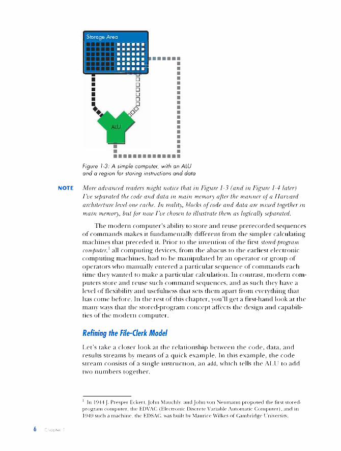
Figure 1-3: A simple computer, with an ALU and a region for storing instructions and data
NOTE More advanced readers might notice that in Figure 1-3 (and in Figure 1-4 later) I ’ve separated the code and data in main memory after the manner of a Harvard architecture level-one cache. In reality, blocks of code and data are mixed together in main memory, but for now I ’ve chosen to illustrate them as logically separated.
The modern computer’s ability to store and reuse prerecorded sequences of commands makes it fundamentally different from the simpler calculating- machines that preceded it. Prior to the invention of the first stored-program computer} all computing devices, from the abacus to the earliest electronic computing machines, had to be manipulated by an operator or group of operators who manually entered a particular sequence of commands each time they wanted to make a particular calculation. In contrast, modern computers store and reuse such command sequences, and as such they have a level of flexibility and usefulness that sets them apart from everything that has come before. In the rest of this chapter, you’ll get a first-hand look at the many ways that the stored-program concept affects the design and capabilities of the modern computer.
Refining the File-Clerk Model
Let’s take a closer look at the relationship between the code, data, and results streams by means of a quick example. In this example, the code stream consists of a single instruction, an add, which tells the ALU to add two numbers together.
6 C h a p t e r ]
1 In 1944J. Presper Eckert, John Mauchly, and John von Neumann proposed the first stored- program computer, the EDVAC (Electronic Discrete Variable Automatic Computer), and in 1949 such a machine, the EDSAC, was built by Maurice Wilkes of Cambridge University.

The add instruction travels from code storage to the ALU. For now, let’s not concern ourselves with how the instruction gets from code storage to the ALU; let’s just assume that it shows up at the ALU’s code input port announcing that there is an addition to be carried out immediately. The ALU goes through the following sequence of steps:
1. Obtain the two numbers to be added (the input operands) from datastorage.
2. Add the numbers.3. Place the results back into data storage.
The preceding example probably sounds simple, but it conveys the basic manner in which computers— all computers—operate. Computers are fed a sequence of instructions one by one, and in order to execute them, the computer must first obtain the necessary data, then perform the calculation specified by the instruction, and finally write the result into a place where the end user can find it. Those three steps are carried out billions of times per second on a modern CPU, again and again and again. It’s only because the computer executes these steps so rapidly that it’s able to present the illusion that something much more conceptually complex is going on.
To return to our file-clerk analogy, a computer is like a file clerk who sits at his desk all day waiting for messages from his boss. Eventually, the boss sends him a message telling him to perform a calculation on a pair of numbers. The message tells him which calculation to perform, and where in his personal filing cabinet the necessary numbers are located. So the clerk first retrieves the numbers from his filing cabinet, then performs the calculation, and finally places the results back into the filing cabinet. It’s a boring, mindless, repetitive task that’s repeated endlessly, day in and day out, which is precisely why we’ve invented a machine that can do it efficiendy and not complain.
The Register FileSince numbers must first be fetched from storage before they can be added, we want our data storage space to be as fast as possible so that the operation can be carried out quickly. Since the ALU is the part of the processor that does the actual addition, we’d like to place the data storage as close as possible to the ALU so it can read the operands almost instantaneously. However, practical considerations, such as a CPU’s limited surface area, constrain the size of the storage area that we can stick next to the ALU. This means that in real life, most computers have a relatively small number of very fast data storage locations attached to the ALU. These storage locations are called registers, and the first *86 computers only had eight of them to work with. These registers, which are arrayed in a storage structure called a register fik, store only a small subset of the data that the code stream needs (and we’ll talk about where the rest of that data lives shortly).
B a s i c C o m p u t in g C o n c e p t s

Building on our previous, three-step description of what goes on when a computer’s ALU is commanded to add two numbers, we can modify it as follows. To execute an add instruction, the ALU must perform these steps:
1. Obtain the two numbers to be added (the input operands) from two source registers.
2. Add the numbers.3. Place the results back in a destination register.
For a concrete example, let’s look at addition on a simple computer with only four registers, named A, B, C, and D. Suppose each of these registers contains a number, and we want to add the contents of two registers together and overwrite the contents of a third register with the resulting sum, as in the following operation:
Code Comments
A + B = C Add the contents of registers A and B, and place the result in C, overwriting whatever was there.
Upon receiving an instruction commanding it to perform this addition operation, the ALU in our simple computer would carry out the following- three familiar steps:
1. Read the contents of registers A and B.2. Add the contents of A and B.3. Write the result to register C.
NOTE You should recognize these three steps as a more specific form of the read-modify-write sequence from earlier, where the generic modify step is replaced with an addition operation.
This three-step sequence is quite simple, but it’s at the very core of how a microprocessor really works. In fact, if you glance ahead to Chapter 10’s discussion of the PowerPC 970’s pipeline, you’ll see that it actually has separate stages for each of these three operations: stage 12 is the register read step, stage 13 is the actual execute step, and stage 14 is the write-back step. (Don’t worry if you don’t know what a pipeline is, because that’s a topic for Chapter 3.) So the 970’s ALU reads two operands from the register file, adds them together, and writes the sum back to the register file. If we were to stop our discussion right here, you’d already understand the three core stages of the 970’s main integer pipeline—all the other stages are either just preparation to get to this point or they’re cleanup work after it.
RAM: When Registers Alone Won't Cut It
8 C h a p t e r ]
Obviously, four (or even eight) registers aren’t even close to the theoretically infinite storage space I mentioned earlier in this chapter. In order to make a viable computer that does useful work, you need to be able to store very large

data sets. This is where the computer’s main memory comes in. Main memory, which in modern computers is always some type of random access memory (RAM), stores the data set on which the computer operates, and only a small portion of that data set at a time is moved to the registers for easy access from the ALU (as shown in Figure 1-4).
□□□□
Registers
Figure 1-4: A computer with a register file
Figure 1-4 gives only the slightest indication of it, but main memory is situated quite a hit farther away from the ALU than are the registers. In fact, the ALU and the registers are internal parts of the microprocessor, but main memory is a completely separate component of the computer system that is connected to the processor via the memory bus. Transferring data between main memory and the registers via the memory bus takes a significant amount of time. Thus, if there were no registers and the ALU had to read data direcdy from main memory for each calculation, computers would run very slowly. However, because the registers enable the computer to store data near the ALU, where it can be accessed nearly instantaneously, the computer’s computational speed is decoupled somewhat from the speed of main memory. (We’ll discuss the problem of memory access speeds and computational performance in more detail in Chapter 11, when we talk about caches.)
The File-Clerk Model Revisited and Expanded
To return to our file-clerk metaphor, we can think of main memory as a document storage room located on another floor and the registers as a small, personal filing cabinet where the file clerk places the papers on which he’s currently working. The clerk doesn’t really know anything
B a s i c C o m p u t in g C o n c e p t s

about the document storage room—what it is or where it’s located—because his desk and his personal filing cabinet are all he concerns himself with. For documents that are in the storage room, there’s another office worker, the office secretary, whose job it is to locate files in the storage room and retrieve them for the clerk.
This secretary represents a few different units within the processor, all of which we’ll meet Chapter 4. For now, suffice it to say that when the boss wants the clerk to work on a file that’s not in the clerk’s personal filing- cabinet, the secretary must first be ordered, via a message from the boss, to retrieve the file from the storage room and place it in the clerk’s cabinet so that the clerk can access it when he gets the order to begin working on it.
An Example: Adding Two Numbers
To translate this office example into computing terms, let’s look at how the computer uses main memory, the register file, and the ALU to add two numbers.
To add two numbers stored in main memory, the computer must perform these steps:
1. Load the two operands from main memory into the two source registers.2. Add the contents of the source registers and place the results in the
destination register, using the ALU. To do so, the ALU must perform these steps:a. Read the contents of registers A and B into the ALU’s input ports.b. Add the contents of A and B in the ALU.c. Write the result to register C via the ALU’s output port.
3. Store the contents of the destination register in main memory.
Since steps 2a, 2b, and 2c all take a trivial amount of time to complete, relative to steps 1 and 3, we can ignore them. Hence our addition looks like this:
1. Load the two operands from main memory into the two source registers.2. Add the contents of the source registers, and place the results in the des
tination register, using the ALU.3. Store the contents of the destination register in main memory.
The existence of main memory means that the user—the boss in our filing-clerk analogy—must manage the flow of information between main memory and the CPU’s registers. This means that the user must issue instructions to more than just the processor’s ALU; he or she must also issue instructions to the parts of the CPU that handle memory traffic.Thus, the preceding three steps are representative of the kinds of instructions you find when you take a close look at the code stream.
10 C h a p t e r ]

A Closer Look at the Code Stream: The ProgramAt the beginning of this chapter, I defined the code stream as consisting of “an ordered sequence of operations,” and this definition is fine as far as it goes. But in order to dig deeper, we need a more detailed picture of what the code stream is and how it works.
The term operations suggests a series of simple arithmetic operations like addition or subtraction, but the code stream consists of more than just arithmetic operations. Therefore, it would be better to say that the code stream consists of an ordered sequence of instructions. Instructions, generally speaking, are commands that tell the whole computer—not just the ALU, but multiple parts of the machine—exactly what actions to perform. As we’ve seen, a computer’s list of potential actions encompasses more than just simple arithmetic operations.
General Instruction Types
Instructions are grouped into ordered lists that, when taken as a whole, tell the different parts of the computer how to work together to perform a specific task, like grayscaling an image or playing a media file. These ordered lists of instructions are called programs, and they consist of a few basic types of instructions.
In modern RISC microprocessors, the act of moving data between memory and the registers is under the explicit control of the code stream, or program. So if a programmer wants to add two numbers that are located in main memory and then store the result back in main memory, he or she must write a list of instructions (a program) to tell the computer exactly what to do. The program must consist of:
• a load instruction to move the two numbers from memory into the registers
• an add instruction to tell the ALU to add the two numbers• a store instruction to tell the computer to place the result of the addition
hack into memory, overwriting whatever was previously there
These operations fall into two main categories:
Arithmetic instructionsThese instructions tell the ALU to perform an arithmetic calculation (for example, add, sub, mul, div).
Memory-access instructionsThese instructions tell the parts of the processor that deal with main memory to move data from and to main memory (for example, load and store).
NOTE We’ll discuss a third type of instruction, the branch instruction, shortly. Branchinstructions are technically a special type of memory-access instruction, but they access code storage instead of data storage. Still, it’s easier to treat branches as a third category of instruction.
B a s i c C o m p u t in g C o n c e p t s

The arithmetic instruction fits with our calculator metaphor and is the type of instruction most familiar to anyone who’s worked with computers. Instructions like integer and floating-point addition, subtraction, multiplication, and division all fall under this general category.
NOTE In order to simplify the discussion and reduce the number of terms, I ’m temporarily including logical operations like AND, OR, NOT, NOR, and so on, under the general heading of arithmetic instructions. The difference between arithmetic and logical operations will be introduced in Chapter
The memory-access instruction is just as important as the arithmetic instruction, because without access to main memory’s data storage regions, the computer would have no way to get data into or out of the register file.
To show you how memory-access and arithmetic operations work together within the context of the code stream, the remainder of this chapter will use a series of increasingly detailed examples. All of the examples are based on a simple, hypothetical computer, which I’ll call the DLW-1.2
The DLW-1's Basic Architecture and Arithmetic Instruction Format
The DLW-1 microprocessor consists of an ALU (along with a few other units that I’ll describe later) attached to four registers, named A, B, C, and D for convenience. The DLW-1 is attached to a bank of main memory that’s laid out as a line of 256 memory cells, numbered #o to #255. (The number that identifies an individual memory cell is called an address.)
The DLW-1's Arithmetic Instruction Format
All of the DLW-1’s arithmetic instructions are in the following instruction format
instruction sourcel, source2, destination
There are four parts to this instruction format, each of which is called a field. The instruction field specifies the type of operation being performed (for example, an addition, a subtraction, a multiplication, and so on). The two source fields tell the computer which registers hold the two numbers being operated on, or the operands. Finally, the destination field tells the computer which register to place the result in.
As a quick illustration, an addition instruction that adds the numbers in registers A and B (the two source registers) and places the result in register C (the destination register) would look like this:
Code Comments
add A, B, C Add the contents of registers A and B and place the result in C, overwriting whatever was previously there.
2 “DLW” in honor of the DLX architecture used by Hennessy and Patterson in their books on computer architecture.
12 C h a p t e r ]

The DLW-l's Memory Instruction Format
In order to get the processor to move two operands from main memory into the source registers so they can be added, you need to tell the processor explicidy that you want to move the data in two specific memory cells to two specific registers. This “filing” operation is done via a memory-access instruction called the load.
As its name suggests, the load instruction loads the appropriate data from main memory into the appropriate registers so that the data will be available for subsequent arithmetic instructions. The store instruction is the reverse of the load instruction, and it takes data from a register and stores it in a location in main memory, overwriting whatever was there previously.
All of the memory-access instructions for the DLW-1 have the following- instruction format:
instruction source, destination
For all memory accesses, the instruction field specifies the type of memory operation to be performed (either a load or a store). In the case of a load, the source field tells the computer which memory address to fetch the data from, while the destination field specifies which register to put it in. Conversely, in the case of a store, the source field tells the computer which register to take the data from, and the destination field specifies which memory address to write the data to.
An Example DLW-1 Program
Now consider Program 1-1, which is a piece of DLW-1 code. Each of the lines in the program must be executed in sequence to achieve the desired result.
Line Code Comments
i load #12, A Read the contents of memory cell #12 into register A.
2 load #13, B Read the contents of memory cell #13 into register B.
3 add A, B, C Add the numbers in registers A and B and store the result in C.
4 store C, #14 Write the result of the addition from register C into memory cell #14-
Program 1-1: Program to add two numbers from main memory
Suppose the main memory looked like the following before running Program 1-1.
#11 #12 #13 #14
12 6 2 3
B a s i c C o m p u t in g C o n c e p t s

After doing our addition and storing the results, the memory would be changed so that the contents of cell #14 would be overwritten by the sum of cells #12 and #13, as shown here:
#11 #12 #13 #14
12 6 2 8
A Closer Look at Memory Accesses: Register vs. ImmediateThe examples so far presume that the programmer knows the exact memory location of every number that he or she wants to load and store. In other words, it presumes that in composing each program, the programmer has at his or her disposal a list of the contents of memory cells #o through #255.
While such an accurate snapshot of the initial state of main memory may be feasible for a small example computer with only 256 memory locations, such snapshots almost never exist in the real world. Real computers have billions of possible locations in which data can be stored, so programmers need a more flexible way to access memory, a way that doesn’t require each memory access to specify numerically an exact memory address.
Modern computers allow the contents of a register to be used as a memory address, a move that provides the programmer with the desired flexibility. But before discussing the effects of this move in more detail, let’s take one more look at the basic add instruction.
Immediate Values
All of the arithmetic instructions so far have required two source registers as input. However, it’s possible to replace one or both of the source registers with an explicit numerical value, called an immediate value. For instance, to increase whatever number is in register A by 2, we don’t need to load the value 2 into a second source register, like B, from some cell in main memory that contains that value. Rather, we can just tell the computer to add 2 to A direcdy, as follows:
Code Comments
add A, 2, A Add 2 to the contents of register A and place the result back into A, overwriting whatever was there.
14 C h a p t e r ]

I’ve actually been using immediate values all along in my examples, but just not in any arithmetic instructions. In all of the preceding examples, each load and store uses an immediate value in order to specify a memory address. So the #12 in the load instruction in line 1 of Program 1-1 is just an immediate value (a regular whole number) prefixed by a # sign to let the computer know that this particular immediate value is a memory address that designates a cell in memory.
Memory addresses are just regular whole numbers that are specially marked with the # sign. Because they’re regular whole numbers, they can be stored in registers—and stored in memory—just like any other number. Thus, the whole-number contents of a register, like D, could be construed by the computer as representing a memory address.
For example, say that we’ve stored the number 12 in register D, and that we intend to use the contents of D as the address of a memory cell in Program 1-2.
Line Code Comments
1 load #D, A Read the contents of the memory cell designated by the number stored in D (where D = 12) into register A.
2 load #13, B Read the contents of memory cell #13 into register B.
3 add A, B, C Add the numbers in registers A and B and store the result in C.
4 store C, #14 Write the result of the addition from register C into memory cell #14-
Program 1-2: Program to add two numbers from main memory using an address stored in a register
Program 1-2 is essentially the same as Program 1-1, and given the same input, it yields the same results. The only difference is in line 1:
Program 1 -1, Line 1 Program 1 -2, Line 1
load #12, A load #D, A
Since the content of D is the number 12, we can tell the computer to look in D for the memory cell address by substituting the register name (this time marked with a # sign for use as an address), for the actual memory cell number in line 1 ’s load instruction. Thus, the first lines of Programs 1-1 and 1-2 are functionally equivalent.
This same trick works for store instructions, as well. For example, if we place the number 14 in D we can modify the store command in line 4 of Program 1-1 to read as follows: store C, #D. Again, this modification would not change the program’s output.
B a s i c C o m p u t in g C o n c e p t s

Because memory addresses are just regular numbers, they can be stored in memory cells as well as in registers. Program 1-3 illustrates the use of a memory address that’s stored in another memory cell. If we take the input for Program 1-1 and apply it to Program 1-3, we get the same output as if we’d just run Program 1-1 without modification:
Line Code Comments
1 load #11, D Read the contents of memory cell #11 into D.
2 load #D, A Read the contents of the memory cell designated by the number in D (where D = 12) into register A.
3 load #13, B Read the contents of memory cell #13 into register B.
4 add A, B, C Add the numbers in registers A and B and store the result in C.
5 store C, #14 Write the result of the addition from register C into memory cell #14.
Program 1-3: Program to add two numbers from memory using an address stored in a memory cell.
The first instruction in Program 1-3 loads the number 12 from memory cell #11 into register D. The second instruction then uses the content of D (which is the value 12) as a memory address in order to load register A into memory location #12.
But why go to the trouble of storing memory addresses in memory cells and then loading the addresses from main memory into the registers before they’re finally ready to be used to access memory again? Isn’t this an overly complicated way to do things?
Actually, these capabilities are designed to make programmers’ lives easier, because when used with the register-relative addressing technique described next they make managing code and data traffic between the processor and massive amounts of main memory much less complex.
Register-Relative Addressing
In real-world programs, loads and stores most often use register-relative addressing, which is a way of specifying memory addresses relative to a register that contains a fixed base address.
For example, we’ve been using D to store memory addresses, so let’s say that on the DLW-1 we can assume that, unless it is explicidy told to do otherwise, the operating system always loads the starting address (or base address) of a program’s data segment into D. Remember that code and data are logically separated in main memory, and that data flows into the processor from a data storage area, while code flows into the processor from a special code storage area. Main memory itself is just one long row of undifferentiated memory cells, each one byte in width, that store numbers. The computer carves up this long row of bytes into multiple segments, some of which store code and some of which store data.
16 C h a p t e r ]

A data segment is a block of contiguous memory cells that a program stores all of its data in, so if a programmer knows a data segment’s starting- address (base address) in memory, he or she can access all of the other memory locations in that segment using this formula:
base address + offset
where offset is the distance in bytes of the desired memory location from the data segment’s base address.
Thus, load and store instructions in DLW-1 assembly would normally look something like this:
Code Comments
load #(D + 108)j A store B, #(D + 108)
Read the contents of the memory cell at location #(D + 108) into A. Write the contents of B into the memory cell at location #(D + 108).
In the case of the load, the processor takes the number in D, which is the base address of the data segment, adds 108 to it, and uses the result as the load’s destination memory address. The store works in the exact same way.
Of course, this technique requires that a quick addition operation (called an address calculation) be part of the execution of the load instruction, so this is why the load-store units on modern processors contain very fast integer addition hardware. (As we’ll learn in Chapter 4, the load-store unit is the execution unit responsible for executing load and store instructions, just like the arithmetic-logic unit is responsible for executing arithmetic instructions.)
By using register-relative addressing instead of absolute addressing (in which memory addresses are given as immediate values), a programmer can write programs without knowing the exact location of data in memory. All the programmer needs to know is which register the operating system will place the data segment’s base address in, and he or she can do all memory accesses relative to that base address. In situations where a programmer uses absolute addressing, when the operating system loads the program into memory, all of the program’s immediate address values have to be changed to reflect the data segment’s actual location in memory.
Because both memory addresses and regular integer numbers are stored in the same registers, these registers are called general-purpose registers (GPRs). On the DLW-1, A, B, C, and D are all GPRs.
B a s i c C o m p u t in g C o n c e p t s