© copyright 2016 md golam rabbani
TRANSCRIPT

© Copyright 2016
Md Golam Rabbani

Modeling and characterization of photoresponse of nanowires with asymmetric
contacts and bending strain
Md Golam Rabbani
A dissertation
submitted in partial fulfillment of the
requirements for the degree of
Doctor of Philosophy
University of Washington
2016
Reading Committee:
Manjeri P. Anantram, Chair
Robert Bruce Darling
Lih Y. Lin
Program Authorized to Offer Degree:
Electrical Engineering

University of Washington
Abstract
Modeling and characterization of photoresponse of nanowires with asymmetric contacts and
bending strain
Md Golam Rabbani
Chair of the Supervisory Committee:
Professor Manjeri P. Anantram
Electrical Engineering
This work investigates (i) contact asymmetry induced response of semiconductors, with
emphasis on nanowire photo response, and (ii) strain induced electronic and optoelectronic
properties of narrow silicon nanowires. Contact area asymmetry is shown to produce large zero-
bias photo response in bulk silicon, which is explained by TCAD modeling. Modeling also
shows that both short circuit current and open circuit voltage in nanowire solar cells and photo
sensors can be enhanced by using contact metals with large work function difference. This does
not need any p-n junction type asymmetric band structure device that requires high and
controlled doping. However, two-contact large nanowires are found to suffer from low current
density due to minority carrier recombination and inefficient carrier collection at contacts. As a
solution, multi-contact and grounded-gate designs are modeled and found to enhance photo

response. By simple fabrication and characterization, we show that nanowire networks with dual-
metal contacts produce large photo currents. Interestingly, a sparse network gives larger response
than a relatively dense network. High resistance nanowire-nanowire contact is shown to place a
limit on electrical transport and explains such unintuitive response. Finally, Molecular dynamics
and quantum mechanical transport simulation of bent narrow silicon nanowires show that
bending strain causes larger decrease in transmission gap compared to the usually investigated
uniaxial strain and that a moderate amount of bending strain may be capable of causing a
semiconductor to metal transition.

i
TABLE OF CONTENTS
List of Figures ................................................................................................................................ iv
List of Tables ............................................................................................................................... viii
Chapter 1. Introduction ................................................................................................................... 1
1.1 Asymmetric Contact Silicon Photo Sensor ..................................................................... 5
1.2 Light-Nanowire Interaction ............................................................................................ 6
1.3 Properties of Bent Silicon Nanowires ............................................................................. 7
1.4 Outline of the Thesis ....................................................................................................... 8
Chapter 2. Photoresponse of silicon with asymmetric area contacts ............................................ 10
2.1 Introduction ................................................................................................................... 10
2.2 Theory of Metal-Semiconductor-Metal Photo Sensors ................................................ 12
2.3 Device Fabrication ........................................................................................................ 14
2.4 Experimental Results and Discussions ......................................................................... 15
2.5 Device Simulation and Modeling ................................................................................. 20
2.6 Conclusion .................................................................................................................... 25
Chapter 3. Modeling of dual-metal contact based silicon micro and nano wire solar cells ......... 26
3.1 Introduction ................................................................................................................... 26
3.2 Device Structure, Problem Statement, and Simulation Method ................................... 27
3.3 Simulation versus Analytical Solutions ........................................................................ 32
3.4 Photocurrent vs. Wire Length ....................................................................................... 37

ii
3.5 Effect of Metal Work Function ..................................................................................... 39
3.6 Short-circuit Current and Open-circuit Voltage ........................................................... 43
3.7 Short-circuit Current Density ........................................................................................ 49
3.8 Comparison with Reported Experimental Results ........................................................ 51
3.9 Improving Short-circuit Current ................................................................................... 51
3.10 Conclusion .................................................................................................................... 55
Chapter 4. Zero-bias Photocurrents in Highly Disordered nanowire networks ............................ 56
4.1 Introduction ................................................................................................................... 56
4.2 Experimental ................................................................................................................. 59
4.2.1 Synthesis of GeNWs and SiNWs .............................................................................. 59
4.2.2 Fabrication of dual-metal test benches on oxide ....................................................... 60
4.2.3 Preparation of nanowire suspension, and dispersion ................................................ 61
4.2.4 Measurement setup ................................................................................................... 62
4.3 Results and Discussions ................................................................................................ 62
4.3.1 Photo response in RD-GeNWs ................................................................................. 62
4.3.2 Photo response in RD-SiNWs ................................................................................... 67
4.3.3 Measurement of metal work function ....................................................................... 69
4.3.4 Discussions ............................................................................................................... 71
4.4 Conclusions ................................................................................................................... 74
Chapter 5. STudy of narrow and bent silicon nanowires .............................................................. 75
5.1 Introduction ................................................................................................................... 75
5.2 Description .................................................................................................................... 78

iii
5.2.1 Nanowire size and shape ........................................................................................... 78
5.2.2 Molecular dynamics .................................................................................................. 81
5.2.3 Procedure of applying bending and uniaxial strain................................................... 81
5.2.4 Strain definition ........................................................................................................ 82
5.2.5 Cropping off nanowire ends...................................................................................... 83
5.2.6 Surface passivation ................................................................................................... 83
5.2.7 Electronic Hamiltonians and their sizes .................................................................... 84
5.2.8 Calculation of electronic transmission ...................................................................... 84
5.3 Results and Discussion ................................................................................................. 85
5.3.1 Strain analysis ........................................................................................................... 85
5.3.2 Electronic transmission ............................................................................................. 95
5.3.3 Bent nanowire vs. uniaxially strained nanowire ....................................................... 98
5.4 Conclusion .................................................................................................................. 100
Chapter 6. Summary and future works ....................................................................................... 101
Bibliography ............................................................................................................................... 105

iv
LIST OF FIGURES
Figure 1.1. Paths of exploration of this work...................................................................... 4
Figure 1.2. Graphical representation of various components of the work. ......................... 5
Figure 2.1. Asymmetric contact photo sensors; asymmetry due to (a) contact size, (b)
light position. ................................................................................................. 13
Figure 2.2. Device fabrication steps. ................................................................................ 15
Figure 2.3. Dark (a), and photo (b) current with bias for different prototype asymmetric-
area contact devices. Inset of (b) shows the zero bias photocurrent for the
same devices. ................................................................................................. 16
Figure 2.4. Current vs time graph display of the light switching with red laser of varying
intensity at zero bias conditions. ................................................................... 17
Figure 2.5. Photocurrent as a function of position. Solid line for green laser and dashed
line for red laser. ............................................................................................ 19
Figure 2.6. Structure of the simulated 2D device where Pad 1 is larger than Pad 2.
Silicon size is 25 μm (horizontal) by 10 μm (vertical). Pad 1 length is
fixed at 2 μm while Pad 2 length is varied. .................................................. 21
Figure 2.7. Current vs voltage profile of two contact device. One contact size is fixed
while the size of the other varies. (a) dark, (b) with light. ............................ 22
Figure 2.8. Current vs light position profile of symmetric device. Light position is
varied. ............................................................................................................ 24
Figure 3.1. Schematic representation of a single nanowire between two metal pads.
Wire dimensions are indicated, and the downward pointing array of green
arrows represents the incident light. .............................................................. 28
Figure 3.2. Comparison of (a) excess electron density and (b) photocurrent from
analytical calculation (solid line) and simulation (symbol). ......................... 35
Figure 3.3. Photocurrent vs wire length for three different minority carrier lifetimes. .... 38

v
Figure 3.4. Conduction (solid), valence (dash) bands and Fermi level (dash dot) for a
10μm long wire. Contact work function pairs are 4.50 eV, 4.50 eV (a), 5.25
eV, 4.75 eV (b), 5.50 eV, 4.50 eV (c), 4.50 eV, 4.00 eV (d). Wire doping
density is 15 -310 cm (p-type, work function is 5.01 eV). Inset of (a) at the top
shows the device schematic, and labels the contacts and the wire. ............... 40
Figure 3.5. Effect of (a) work function and (b) contact doping on short circuit
photocurrent versus device wire length. ........................................................ 42
Figure 3.6. Photocurrent versus bias for different nanowire lengths: (a) 2D simulation
of 1 micrometer wide wire, (b) 3D simulation of 100 nm wide wire. Open
circuit voltage versus device length (c). Both wires have a height of 35 nm.
Minority carrier lifetime is 10μs. .................................................................. 46
Figure 3.7. Available and actual open circuit voltages as a function of intensity. Wire
doping density is 15 -310 cm (p-type, work function is 5.01 eV). Lifetime is
10 μs . ............................................................................................................ 47
Figure 3.8. ISC and VOC as a function of (a) WS, with WO fixed, (b) WO, with WS fixed.
....................................................................................................................... 48
Figure 3.9. Short circuit current density versus wire lengths for three different minority
carrier lifetimes. The wire has a height, H, of 35 nm. ................................... 50
Figure 3.10. Electrically breaking a long wire into a few short wires. ............................. 52
Figure 3.11. Short circuit current (a), and open circuit voltage (b) as a function of
number of pads for six different nanowire lengths. The wire widths and
heights are fixed at 100nm and 35nm, respectively. Minority carrier
lifetime is10μs . ............................................................................................. 53
Figure 3.12. Grounded gate electrode improves both short circuit current and open
circuit voltage. ............................................................................................... 54
Figure 4.1. (a) Fabrication steps for metal patterns on an insulating substrate, (b) I-V
measurement setup. ....................................................................................... 60
Figure 4.2. (a) SEM image of dense RD-GeNWs with Al and Ni contacts (100 µm), (b)
I-V characteristics in the dark (solid) and light (dashed), and (c) light

vi
switching at zero (blue solid, left y-axis) and 5 V (green dashed, right y-
axis) bias in a dense RD-GeNWs device. ...................................................... 63
Figure 4.3. (a) SEM image of sparse Ge-RDNWs with Al and Ni contacts (100 µm),
(b) I-V characteristics in the dark (dashed) and light (solid), (c) Light
switching in sparse Ge-RDNWs device at 5 V (green dashed, right y-axis)
and zero bias (blue solid, left y-axis). ........................................................... 65
Figure 4.4. SEM images of dense (a) and sparse (b) RD-GeNW devices with 10 µm
metal gap, (c) I-V characteristics in dark and light, and (d) light switching
at zero bias. .................................................................................................... 66
Figure 4.5. SEM images of dense (a) and sparse (b) RD-SiNWs devices. I-V
characteristics in the dark and light for both (c) dense and (d) sparse SiNW
devices with a metal gap of 10 µm. The 5 V and zero-bias photo switching
responses for the dense (e) and sparse (f) devices are also shown. ............... 68
Figure 4.6. (a) KPFM scan of a two metal (Nickel and Aluminum) device without
nanowire (b) shows the surface work function along the horizontal line in
(a). .................................................................................................................. 70
Figure 4.7. Energy band diagrams of current path for a single NW (a), and multiple
NWs (b). ........................................................................................................ 71
Figure 4.8. RDNW device schematics. (a) long sparse NW network (inset shows band
structure of a Ni-NW-Al channel), (b) short, sparse NW network (inset
shows band structure of a Ni-NW1-Oxide-NW2-Al channel), (c) long,
dense NW network, inset shows zoom in on one end of some of the top
NWs. .............................................................................................................. 73
Figure 5.1. Nanowire cross section (a), length (b), a few layers along length (c). ........... 80
Figure 5.2. Local strain along the z-direction (length) in 3 different nanowires as a
color plot; (a) <110>3d, (b) <110>5d, (c) <110>7d. .................................... 87
Figure 5.3. Local strain along the x-direction in 3 different nanowires as a color plot;
(a) <110>3d, (b) <110>5d, (c) <110>7d. ...................................................... 88
Figure 5.4. Local strain along the y-direction in 3 different nanowires as a color plot;
(a) <110>3d, (b) <110>5d, (c) <110>7d. ...................................................... 89

vii
Figure 5.5. Local strain along (a) z, (b) x, (c) y direction as a color plot for a uniaxially
strained <110>5d nanowire. .......................................................................... 90
Figure 5.6. Ranges of strain (x-range (a), y-range, (b) and z-range (c)) as functions of
nanowire diameter for different amount of end atom group rotations. ......... 92
Figure 5.7. Layer to layer average strain along length. (a) <110>3d, and (b) <110>6d... 93
Figure 5.8. Average strain along length of a bent nanowire as a function of diameter. ... 94
Figure 5.9. Electronic transmission as a function of energy. (a) <110>2d with no
rotation, (b) <110>2d with 15 degree rotation, (c) <110>4d with no
rotation, (d) <110>4d with 15 degree rotation, (e) <110>6d with no
rotation, (f) <110>6d with 15 degree rotation. .............................................. 95
Figure 5.10. Transmission gap as a function of nanowire diameter for different rotation
angles. ............................................................................................................ 97
Figure 5.11. Transmission gap as a function of % strain. Solid: bent, dashed: uniaxial. . 98
Figure 5.12. Ec and EV as a function of % strain. Solid: bent, dashed: uniaxial. ............ 99
viii
LIST OF TABLES
Table 3.1. List of variables ............................................................................................... 30
Table 3.2. List of constants ............................................................................................... 30
Table 4.1. Ge and Si NW samples studied in this chapter. The terms Dense and Sparse
used in the text refer to the concentrations in this table, unless explicitely
stated otherwise. .............................................................................................. 62

ix
ACKNOWLEDGEMENTS
I am grateful to my advisor, Professor Manjeri P. Anantram, for his guidance, encouragements as
well as support throughout my doctoral study. His vast knowledge, great courses, and attention to
details have helped my research move forward and be less error prone.
I would like to thank Professors R. Bruce Darling and Lih Y. Lin for serving in my reading
committee. Professor Darling has also been a great help throughout my PhD study in UW by
sharing his vast knowledge, teaching me device and fabrication, and allowing me access to his lab.
In addition to teaching two valuable courses, Professor Lin has often lent helping hands with access
to her lab and instruments.
I am fortunate to have had an impressive list of collaborators: Professors Amit Verma, Reza
Nekovei, and Mahmoud Khader. Professor Verma’s constant interest, motivation and support
helped me move ahead during rough periods in my research. Professor Nekovei provided
important characterization instrument. Professor Khader made great efforts so that I had had access
to useful instruments. I thank also Professor Brian Korgel and Julian Villarreal from UT Austin
for providing nanowires and helps in improving a research paper. I highly appreciate help and
guidance from Professor Sunil Patil of Pune College of Engineering.
I thank National Science Foundation and QNRF for generously supporting my research.
My research was partly carried out in EE fabrication and characterization lab, Washington
Nanofabrication Facility and Molecular Analysis facility. My thanks go to the helpful staffs in

x
these facilities. I will be forever indebted to EE department and its staffs and the UW as a whole
for my happy and fruitful time in Seattle.
Finally, I thank my family for their love, support and sacrifice. My mother was not pleased
with my leaving Bangladesh for my PhD but would be so happy when I would call her on phone.
Unfortunately, she suddenly passed away while I was so far away from her. I love you Ma and
miss you every single day. My father has had to work really hard to raise my brother and me. He
always believed in me and my education. I hope to be as good a father as he is. My wife, Sheuli,
has taken care of my whole family, always encouraged me, and reminded me of how important it
was to not give up when I was down. My son, Anubhav, has been a great source of joy. Every day
I look forward to returning home for his welcoming smile and hug. He is my sweetheart #0-13.

xi
DEDICATION
To the loving memory of my mother.

1
Chapter 1. INTRODUCTION
Over the past two decades, semiconductor nanowires have received widespread attention in
nanoscale research areas such as nano-electronics and nano-photonics. Nanowires can function as
miniaturized devices as well as electrical interconnects. As such, they are being considered as
important building blocks in nanotechnology. They have unique shapes, sizes, compositions,
chemical and physical properties, which can now be controlled with relative ease as a result of
worldwide efforts in nanomaterials research. Their high aspect ratio allows the bridging of the
nanoscopic and macroscopic worlds, which is fundamental to the integration of electronics and
photonics.
Bulk silicon is the most widely used semiconductor in electronics and photovoltaics. Recently,
silicon nanowire has also been established as a major player in nanotechnology. The nanowires
can be fabricated in both top-down and bottom-up approaches, and have been fabricated in a range
of diameters, from a few nanometers to a few hundred nanometers. Due to its indirect band gap,
bulk silicon’s photo absorption efficiency is low. Hence a thick film of silicon is necessary for the
complete absorption of solar spectrum. Thick film requires more materials and increases the
associated material cost. However, silicon nanowires (SiNWs) have been found to have a
considerably improved light absorption property [1]–[6]. Since a smaller amount of material (i.e.
nanowires) can absorb a larger fraction of the incident light, this may result in huge saving in the
material cost. SiNWs are thus very promising for photosensing and photovoltaic applications, and
have already been used in many photodetectors [7]–[10] and solar cells [1], [3], [11]. In addition
to SiNWs, our results are relevant to other nanowires in general and we have also studied
germanium nanowires (GeNWs).

Many of the improved properties of nanowires have been attributed to their having a large
surface to volume ratio [12]–[16]. However, the large surface is also often associated with a large
surface roughness [17], [18], which increases scattering and thereby degrades thermal and
electrical mobility, and reduces carrier lifetime (or diffusion length). Low minority carrier lifetime
(diffusion length) is a big issue in the photosensing and photovoltaic applications of nanowire
devices because the collection of the photo generated carriers, hence the efficiency, in such devices
is greatly reduced. This issue can be alleviated through improved device designs, such as using a
core-shell structure [11], [19], [20] instead of an axial device. I present a distributed contact design
to increasing the photo generated carrier collection, especially in long nanowires, as discussed in
Chapter 3. The distributed contacts divide a long (compared to the carrier diffusion length)
nanowire into many small wires in parallel, and improve both short circuit current and open circuit
voltage.
Some sort of asymmetry in the device improves the carrier collection efficiency as photo
generated electrons can flow towards one contact while holes flow towards the other. The usual
approach to introducing asymmetry is through the formation of a p-n junction by doping [21]–
[23]. Achieving a precisely controlled doping in nanodevices is, however, difficult [24]–[27]. As
a solution, we show that appropriately chosen metal pairs (that is, metal contacts having sufficient
work function difference) can achieve the same performance as a p-n junction type device without
any need for large and controlled doping densities. In such a design, compared to the nanowire
work function, one contact has a higher work function while the other contact has a lower work
function. We develop a guideline for choosing the metal pair which has the required work function
asymmetry and avoids deleterious effects such as reduction of minority carrier lifetime.

Study of very narrow silicon nanowires have revealed that, unlike bulk silicon and wide
nanowires, they have a direct bandgap [28], [29], which is essential for efficient light absorption
and emission. More importantly, it has also been found [30] that mechanical strain can change the
amount of bandgap and turn a direct bandgap semiconductor into an indirect bandgap
semiconductor, and vice versa. These results are very promising for optoelectronic applications of
SiNWs, such as for fabricating tunable lasers. So far, strain dependent electronic studies of
nanowires have exclusively focused on uniaxial strain, despite most real nanowires having some
bending inherently present in them. Such as, bottom up synthesized nanowires are usually not
perfectly straight, rather they are twisted as well as jumbled [31], [32]. In reference [33],
Bertagnolli grew wires with a predefined rectangular shape. Zhu et al. [34] demonstrated over 40%
bending strain in nanowires with tungsten tip. In an ultimate bending strength experiment, Cook
et al. [35] bent silicon nanowires lying on a flat substrate through sequential atomic force
microscope (AFM) tip manipulations. They could get a U-shape bending, and found that, as
diameter decreased, the amount of bending that the nanowires could withstand before breaking
increased. This might mean that the narrower nanowires are more stable under larger bending
stresses. Although these bending studies have been done mostly on bottom up nanowires, even
top-down fabricated nanowires can be bent intentionally [36], [37] or unintentionally [38], [39].
Moreover, top down and bottom up approaches can be combined [40] to get horizontally
suspended, well-oriented and size-controlled nanowire arrays. Due to bending, as opposed to
uniaxial straining, different atoms in the nanowire are under different amount of strain. This may
open up new possibilities, and electronic and optoelectronic studies of bent wires are necessary.
In view of the opportunities and challenges discussed above, we study the response of
nanowires to light as well as to strain. Figure 1.1 below lists the exploration paths as well as the

application areas of this work. The targeted fields are photodetection, photovoltaic and strain
dependent electro-optic devices. In these areas, we explore how asymmetry - in both size and work
function - in device metal contact affects device characteristics under light. We show that,
depending on the nanowire length, the optimum number of contacts may be different for efficient
carrier collection. Besides single nanowires, devices consisting of nanowire networks are relatively
easier to fabricate. Our investigation shows that they produce considerable amount of photo
response which depends on network density in an unintuitive way. Role of strain in modifying
electrical properties, such as bandgap, conductivity, are also to be studied through simulations.
Figure 1.1. Paths of exploration of this work.
Figure 1.2 schematically specifies the various components of the proposed work. In Figure
1.2(a), a nanowire is lying on an insulating substrate. The substrate mainly provides mechanical
support. There is one metal contact on each of the two ends of the nanowire. This device is also
assumed to be in the dark (no light) condition. Such is the reference device. The other parts of

Figure 1.2 all show some particular changes with respect to the reference device. Figure 1.2(b)
turns on illumination. Figure 1.2(c) depicts the case with a different metal for the second contact
while the nanowire is under illumination. The nanowire is under strain in Figure 1.2(d).
Figure 1.2. Graphical representation of various components of the work.
The major divisions of this work are briefly touched upon in the following sections. Later
chapters will have more on each of these.
1.1 ASYMMETRIC CONTACT SILICON PHOTO SENSOR
Although we will be mostly dealing with nanowires in this study, first, we want to present some
interesting results from metal-on-bulk-silicon based photo sensors. Sensing of light is useful in
numerous fields such as radiation detection, smoke detection, flame detection, street light
switching, atomic force microscopy, security alarm, etc. This is a mature field, and there exist
various device designs for realizing a photo sensor. Some examples are photodiode, avalanche
photodiode, PIN photodiode, Schottky diode, phototransistor, and photomultiplier. In the very first
of our experimental processes, we fabricated metal-semiconductor-metal (MSM) devices with
only a single metal deposited on bulk silicon with native oxide. Such simpler devices can have
significant dark leakage suppression [41] and our measurements also reveal that they can have
large photocurrent response, even at zero bias. We show that asymmetry in the physical size of,
and asymmetry in the light position relative to, the metal contacts are the bases for such excellent
photosensing device. Its fabrication process is very simple and low cost. At the same time, its
output photocurrent is large. In Chapter 2, I detail this photo sensor’s theory and fabrication along
with the experimental results.
1.2 LIGHT-NANOWIRE INTERACTION
Due to its indirect band gap, bulk silicon’s photo absorption efficiency is low. However, silicon
nanowires have been found to have a considerably improved light absorption property. This is very
promising for photosensing and photovoltaic applications. These fields are recently seeing huge
research efforts, and there are also increased government subsidies for designing low cost solar
cells. Taking these as motivations, we have simulated both short circuit current and open circuit
voltage of nanowire based photo sensing devices. A simple device with dual-metal contacts has
been studied. Detailed understanding of the influence of wire dimensions, minority carrier
lifetimes, and metal work functions on the optical characteristics has been made. Based on our
findings, we put forth guidelines for choosing the contact metals for higher output efficiency.
Distributed electrode structure has also been shown to increase the short circuit current of long
wires and improve their current density.

Experimental realization of the modeled device has also been done. First simple metal
depositions are performed to fabricate ‘oxide test benches’, each with lines of two different metals
forming gaps on an oxide wafer. Next a nanowire suspension is drop casted on the metal gaps in
the oxide test bench. This deposits a nanowire network which bridges the two metals and forms a
device. Current—voltage and photo switching measurements are done and an appreciable photo
response is achieved. When nanowires are longer than the metal gap size, sparse network gives
larger current than a relatively denser network. We consider details of electronic transport toe
explain such unintuitive phenomenon. We have studied both GeNW and SiNW networks to show
that the results are quite general.
1.3 PROPERTIES OF BENT SILICON NANOWIRES
A strained semiconductor device can have many useful electronic and optoelectronic properties.
Strained bulk silicon has higher electron and hole mobilities [42], [43], which has been found to
improve the switching speed of the transistors. It has also been predicted [30] that strain can change
both size and directness (or indirectness) of the bandgap of narrow silicon nanowires. Such a
property may be important in optoelectronic applications. These works mostly employ uniaxial or
biaxial strain. However, due to intentional or unintentional reasons [44], [45], silicon nanowires
can actually be under quite a large amount of bending strain. Naturally, it is desirable to investigate
their electronic and optoelectronic properties. So we do classical molecular dynamics and quantum
mechanical simulations to understand the strain profile and electronic transmissions in such
nanowires in Chapter 5. Uniaxially strained silicon nanowires of similar sizes have also been
simulated. Comparison shows that, for same average strain, bent nanowires have a larger decrease
in their transmission gap, which represent a larger increase in conductivity.

1.4 OUTLINE OF THE THESIS
This thesis is organized as follows.
1) Before delving into nanowires, we discuss the theory, fabrication and experimental
measurements of photocurrent characteristics of bulk silicon MSM photo sensor
devices in Chapter 2. We describe that asymmetry in (i) physical sizes of two metal
pads and (ii) light position with respect to contact electrodes can produce large
photocurrent.
2) In Chapter 3, we describe simulation and modeling of asymmetric-work-function
metal contacts based nanowire photo sensing devices. Short circuit current, open
circuit voltage and photocurrent densities are studied in detail. Guideline for
choosing appropriate metals is given. Long nanowires with contacts only at the
ends are found to be less efficient in terms of current density. An improved design
with distributed contacts to maximize their output is then proposed. Finally, it is
shown that further performance enhancement can be achieved with gated diode
design, which also produced a small negative differential resistance (NDR) effect.
3) In Chapter 4, fabrication and characterization of nanowire network based two
contact photo sensors are presented. It is found that, although the fabrication
approach is very simple, the devices produce appreciable amount of photo currents.
Depending on the relative lengths of the nanowires with respect to the contact to
contact distance, either dense or sparse network may produce more current. The
case of some sparse networks producing relatively larger currents is explained by
considering the detail of the current transport mechanism in the network.

4) Chapter 5 investigates electronic transport properties of strained narrow silicon
nanowires using molecular mechanics and non-equilibrium Green’s function
(NEGF) simulations. Strain variations in the bent nanowires are analyzed in detail.
Then, electronic transmission, and the energy gap therein, are correlated with the
nanowire diameter as well as the amount of bending. Finally, the strain induced
transmission gap change in bent nanowires is compared with the same effect in
similar uniaxially strained nanowires, and it is shown that bent nanowires show a
larger gap decrease for similar strain.
5) The last chapter, Chapter 6, summarizes the thesis and discusses future work
directions

Chapter 2. PHOTORESPONSE OF SILICON WITH ASYMMETRIC
AREA CONTACTS
We report metal-semiconductor-metal (MSM) photo sensors based on asymmetric metal pad areas.
Our photosensor devices displayed strong absorption properties upon exposure to electromagnetic
radiation. Our devices are simple to fabricate, requires a single-step metal deposition, and exhibit
photoresponse even at zero bias conditions. In this chapter, we present a brief discussion on the
theory behind the necessity of asymmetry in contact pads to enhance photoresponse in short circuit,
which is generally achieved by variation in metal work function. In addition, we present the
theoretical explanation and experimental verification with our proposed prototype devices made
of platinum deposited on bulk silicon. Our results display a large photo current and a zero dark
current under zero applied voltage at ambient environmental conditions. Our device offers
excellent light switching behavior that are fast and stable at room temperature, which make them
excellent candidates for innovative devices with extreme stability and reliability.
2.1 INTRODUCTION
Silicon based photosensing is an exciting area of research that finds numerous applications in high-
tech device fabrication industry for integrated active/passive optical components such as filters,
sensors, detectors [46], [47]. These devices are compatible with the low cost complementary metal
oxide semiconductor (CMOS) fabrication process which makes possible having both optical and
electronic circuits in a single microchip [41]. Silicon photo sensors are found in various device
configurations such as photodiode [48], phototransistor [49], [50], simple Schottky diode [51], and
MSM dual Schottky diodes [41], [50]–[56]. The MSM devices hold great potentials due to their
simple fabrication process, low capacitance, ease of integration with preamplifier circuits, large
bandwidth as well as high sensitivity [41], [53]. MSM photo sensors with a single as well as double
metals have been demonstrated in both III-V [54] and IV [41], [52] semiconductors. They,
however, have a relatively large dark current [55], which causes additional power dissipation in
the already hot and densely packed integrated circuits. Most of the remedial efforts so far [41],
[52], [54] are focused towards achieving an asymmetry in the contact metal work functions as well
as replacing the high cost direct bandgap materials with the low cost silicon. Significant
contribution by Okyay et al. [53] discusses the importance of asymmetric area electrodes that can
be utilized to suppress the Schottky diode leakage current. A recent study by Zhang et al presents
the simulation study on the influence of asymmetric electrode structures for effective dark current
suppression in silicon based photodetectors [57]. However, a detailed experimental study of the
photoresponse of such devices, specifically under zero bias conditions is still missing.
In this chapter, we present a thorough experimental analysis on MSM device with metal
contacts of similar workfunction but dissimilar contact areas. The photosensor devices involves a
very simple and cost-effective CMOS fabrication process which includes a one-step metal
deposition on a standard silicon wafer. A large photoresponse is observed, even under low light
and low or zero bias conditions. In addition, we also present the simulation studies on our device
structure which validates the experimental results. This chapter presents a complete discussion on
the theoretical background of the device model followed by the fabrication process, experimental
studies and simulation results. Both dark and light currents measurements were performed with
the prototype devices. Photoresponse of the detector device as a function of laser power and
wavelength is presented here.

2.2 THEORY OF METAL-SEMICONDUCTOR-METAL PHOTO SENSORS
When semiconductor materials, such as silicon, are exposed to electromagnetic radiations, they
absorb part of the light that results in the excitation of its valence band electrons to its conduction
band. The absorption properties of semiconducting materials are dependent upon the electronic
structure of the semiconductor as well as the thickness of the material. The excited electrons in
conduction band participate in charge transport thereby increasing the electrical conductivity of
the material resulting in an improved electrical signal.
In order to obtain a photo current signal from light shining on a piece of semiconductor, the
photo generated carriers inside the material must be collected through the metal contacts. However,
if the numbers of photo-generated electrons (holes) collected at the two contacts are equal, the net
photo current due to electrons (holes) will be zero. This is the general observation in
semiconductors if the two metal pads are identical and the light intensity is uniform all over the
device. Such circumstances are normally overcome by employing either a p-n junction inside the
semiconductor or using two dissimilar metals as two contacts. However, both of these approaches
will take more than one photolithography step. Creating the p-n junction in semiconductor wafer
requires at least one step for doping and another step for the metal deposition. Similarly,
constructing dissimilar metal contacts on semiconductors involve two separate metal deposition
steps.
Here, we propose a one-step lithography process for fabricating asymmetric electrical contacts
based photo sensors. In case of a Schottky contact, the electron transport property of the device
depends upon the contact area between the metal and the semiconductor since the amount of
tunneling is directly proportional to the contact area. Amount of surface recombination will also
depend on the contact size. Hence, if we make the two contacts of a photo sensor with the same
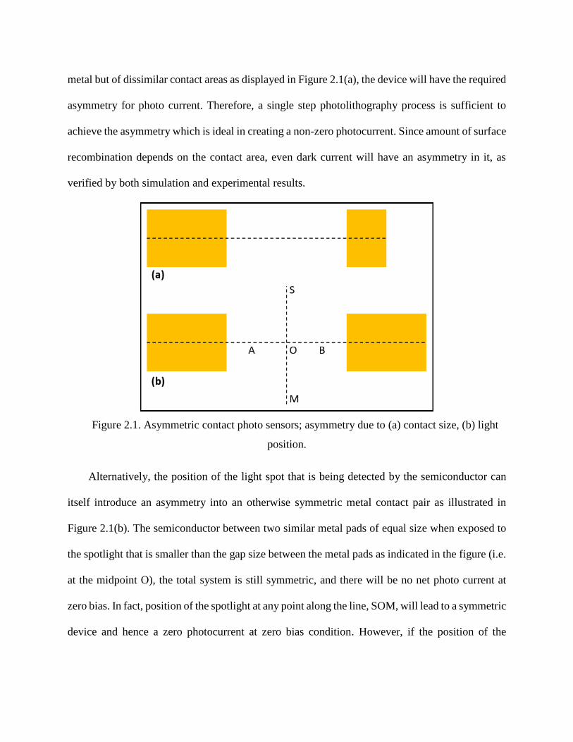
metal but of dissimilar contact areas as displayed in Figure 2.1(a), the device will have the required
asymmetry for photo current. Therefore, a single step photolithography process is sufficient to
achieve the asymmetry which is ideal in creating a non-zero photocurrent. Since amount of surface
recombination depends on the contact area, even dark current will have an asymmetry in it, as
verified by both simulation and experimental results.
Figure 2.1. Asymmetric contact photo sensors; asymmetry due to (a) contact size, (b) light
position.
Alternatively, the position of the light spot that is being detected by the semiconductor can
itself introduce an asymmetry into an otherwise symmetric metal contact pair as illustrated in
Figure 2.1(b). The semiconductor between two similar metal pads of equal size when exposed to
the spotlight that is smaller than the gap size between the metal pads as indicated in the figure (i.e.
at the midpoint O), the total system is still symmetric, and there will be no net photo current at
zero bias. In fact, position of the spotlight at any point along the line, SOM, will lead to a symmetric
device and hence a zero photocurrent at zero bias condition. However, if the position of the

spotlight is deviated from the line SOM, for example at point A or B, an asymmetry is introduced
in the circuit thereby generating a photo current at short circuit.
For both the photo sensors in Figure 2.1, the degree of asymmetry will depend on the light
position with respect to the two contacts, and as a result, the magnitude of photo current will vary
depending on the light position. Considering the device in Figure 2.1(b) and a light source with
constant spot size, light location at point O will give zero photo current due the symmetry as
already discussed. Now as light position moves towards the left contact, along line OA, the current
magnitude will first increase, reach a maximum and then fall off as some of the incident light will
be obstructed by the metal pad, assuming the pad reflects off most of the incident light. If this
current is assumed positive, then a mirror symmetric (negative) current profile will be generated
as the light position moves starting from point O towards the right contact, along line OB.
2.3 DEVICE FABRICATION
Fabrication was done on p-type, 100 mm diameter, and 500 um thick silicon wafer. The process
flow is shown in Figure 2.2. First, the wafer was run through a spin, rinse, dry (SRD) cycle to
clean it. Then, to remove any organic contaminants, barrel etching was done for 5 minutes at 100
W power. Next, standard photolithography was used to pattern resist on the wafer. Briefly, NR7-
1000PY negative resist was spun coated and then baked at 150 C on a hot plate for 60 seconds.
The resist was then exposed and again baked at 100 C for 50 seconds. TMAH based developer,
RD6, was used to develop the resist. This was followed by an SRD cycle. Immediately before
metal deposition, barrel etching was done to remove residual photoresist from the developed away
regions. This etching was done for 30 seconds at 50 W power. Then electron beam assisted
evaporation was done to deposit 10 nm chromium adhesion layer and then 20 nm platinum layer.
Finally, metal liftoff was done in acetone.

Figure 2.2. Device fabrication steps.
2.4 EXPERIMENTAL RESULTS AND DISCUSSIONS
Figure 2.3 shows both dark and photo current as a function of device bias for five different devices
with one large and one small pads. Two probe IV measurements performed to characterize each
and every contact pad revealed the absence of the commonly existing Ohmic behavior in
nanodevice transport properties. This is a clear evidence of the formation of rectifying junction in
our devices. The graph clearly shows the asymmetry in dark current (Figure 2.3(a)) and displays
zero current at zero bias conditions. Our devices exhibited a slow increase in current until a
threshold voltage is achieved due to the presence of the rectifying junction beneath the pads. Upon
exposure to electromagnetic radiations in the visible range, the same set of devices exhibited
photovoltaic properties in all five cases as displayed in Figure 2.3(b). A huge elevation in
photocurrent, up to four orders of magnitude of increase, was observed in all our devices. It is
essential to mention that the position of the spotlight is fixed at the midpoint between the two pads.

Figure 2.3. Dark (a), and photo (b) current with bias for different prototype asymmetric-area
contact devices. Inset of (b) shows the zero bias photocurrent for the same devices.
(a)
(b)

In both photocurrent and dark current asymmetry is observed with bias polarity. Such
asymmetry, we believe, is due to the asymmetry in contact pad areas. In addition, we observed a
photocurrent at zero bias, as shown in the inset of Figure 2.3(b). Our experimental results clearly
show that the contact area asymmetry is effective at producing large photocurrent and dark current
at zero bias.
Figure 2.4. Current vs time graph display of the light switching with red laser of varying
intensity at zero bias conditions.
In an attempt to further explore the robustness of our devices, we have also investigated the
instant photoresponse which is primarily determined by the rate of photo-generation of the charge
carries and we studied the light intensity dependence on the transport properties in asymmetric

contact pads. This study was carried out by shining a red laser of wavelength 650 nm between the
asymmetric contact pads at regular time intervals. The results displayed in Figure 2.4 confirms the
switching behavior of our devices when the light source is turned ON/OFF and its dependence to
variation in intensity, exhibiting larger photocurrent for high power lasers. The dark current is zero
due to the zero applied bias while the observed photocurrent is in tens or hundreds of micro
Amperes. The improved response in the optoelectronic transport properties of our devices can be
explained by the asymmetry in area of contact pads which cause asymmetry in carrier collection.
Area asymmetry is also a factor in I-V characteristics of a Schottky junction [58]. This stimulates
photocurrent. For the results in Figure 2.4, the applied bias between the two metal pads is kept at
zero volt. The laser intensity is varied from 10 mW to 100 mW. However, during each laser ON
period, the intensity is kept constant.
The laser spot position was fixed to a location between the asymmetric metal pads, which
produced maximum photocurrent. As the light source was turned ON and OFF, a rapid switching
behavior is observed. The dark current is zero due to the zero applied bias while the photocurrent,
due to contact area asymmetry, is tens or hundreds of micro Amperes. Based on the behavior of
our devices to high power laser exposure, we believe that a significant photocurrent can be
observed with low power lasers and low intensity light sources.

Figure 2.5. Photocurrent as a function of position. Solid line for green laser and dashed line
for red laser.
We also explored the possibilities of introducing asymmetry in transport properties of our
devices with symmetric contact pads. In such devices, the spot size and position of the light source
played a major role in determining the changes in the magnitude of photocurrent. We were able to
observe the variation in transport properties as the laser spot is swept from one metal pad to the
other. Figure 2.5 present the photocurrent vs time graph of the devices upon exposure to green and
red lasers. The position of the laser spot is moved from the left end toward the right at an
approximately constant velocity. This is achieved by mounting the laser source on a micrometer
moving and rotating the later at a constant speed. As the figure displays, a gradual decrease in
photocurrent was observed as the laser spot moves from left to right. This continued until the

photocurrent attained a negative maximum. With any further change in the position of the laser
spot towards the right contact pad, the photocurrent increased to zero approximately around the
midpoint between the contact pads. Moving on further we observed a similar change in
photocurrent, this time attaining a positive maximum closer to the right contact pad. Based on our
studies on symmetric contact pad devices, we conclude that fixing the position of the light source
at any on the peak positions will yield a significant increase in photocurrent at zero bias conditions,
given that the spot size of the laser is much smaller than the gap between the metal pads. All these
studies are carried out at ambient temperature and pressure conditions using red and green laser
source of approximately 10mW power.
A greater photoresponse with a well-defined peak is observed with red laser which also
exhibited a better symmetry with respect to the midpoint of the contact pads. The larger current
can be attributed to the band gap of the semiconductor silicon and the workfunction of the metal
pads. Also responsivity of silicon increases with wavelength until it reaches a maximum at about
950 nm and then falls of as we approach and go beyond the bandgap.
2.5 DEVICE SIMULATION AND MODELING
Experimental results from our prototype devices verify the theory we presented. Next to gain a
better understanding of the device physics and phenomena responsible for asymmetry and large
short circuit current under light, we model an asymmetric-area-contact device using state-of-the-
art TCAD simulations [59]. For simplicity, we consider a two dimensional (2D) device. Such a
device maintains the underlying physics that we are interested in, i.e., contact size asymmetry, but
reduces the computation cost to a manageable level. It can be assumed that the 2D structure is
taken from a vertical cross-section along the horizontal dashed line in Figure 2.1(a). Figure 2.6
depicts the device that we simulate.

Figure 2.6. Structure of the simulated 2D device where Pad 1 is larger than Pad 2. Silicon
size is 25 μm (horizontal) by 10 μm (vertical). Pad 1 length is fixed at 2 μm while Pad 2 length
is varied.
The silicon size is 25 μm by 10 μm . Doping density is n-type 1015 cm-3 and minority carrier
lifetime of 1 μSec is assumed. Pad 1 length (Figure 2.6) is kept fixed at 2 μm while the length of
Pad 2 is varied to achieve a device with varying amount of asymmetry. The recombination
processes that we consider are Shockley-Read-Hall (SRH) and Auger recombination. In addition,
surface recombination as well as barrier lowering effects have been taken into account as they are
important for a Schottky junction and found to give better match with trends in experimental
results.

Figure 2.7. Current vs voltage profile of two contact device. One contact size is fixed while
the size of the other varies. (a) dark, (b) with light.
(a)
(b)

Figure 2.7 presents the current versus voltage profile of the device in Figure 2.6 for bias range
of -1 V to +1 V in both dark (a) and light (b). The length of Pad 2 is varied from 40 nm to 2 μm .
The asymmetry is obvious; the larger the contact size asymmetry, the larger the asymmetry in
current. At zero applied bias, the dark current is zero irrespective of the contact asymmetry, which
is necessary. However, the zero bias photocurrent is zero only for the symmetric case, that is, when
both contacts are 2 μm long. For asymmetric contacts, large photocurrent, which follows the
contact length asymmetry, is achieved. The current versus voltage profile has some interesting
features: at lower voltage current increases sharply. But at higher voltage, it saturates. The
saturation region has a slope due to barrier lowering in Schottky contact. As the length of the Pad
2 increases, its saturation current also increases, as there are larger and larger contact area for
surface recombination as well as current conduction. The simulation characteristics (Figure 2.7)
match quite well with the experimental results (Figure 2.3).
Some comments on the shape of saturation current versus bias follow. Simulation suggest that
surface recombination alone can account for overall current asymmetry but once saturation is
reached, the current remains flat if only surface recombination effect is taken into account.
However, Schottky barrier lowering with bias is an important effect for metal-semiconductor
junctions and we found that once barrier lowering is considered we recover the slowly increasing
linear I-V in the saturation current as we saw in the experimental I-V.
Next we consider device of the type shown in Figure 2.1(b). As already mentioned, physically
the device is symmetric, but the light spot position can cause an asymmetry if it is smaller than the
anode to cathode gap. Figure 2.8 plots the zero bias photocurrent for three different laser lights as
the position of the light is varied from the leftmost edge to the rightmost of the device shown in

the inset of Figure 2.8. The flat regions are due to the metal contact which does not absorb any
light.
Figure 2.8. Current vs light position profile of symmetric device. Light position is varied.
Two different discrete wavelength lasers - green (532nm) and red (650nm) - have been used
and the photocurrent is found to increase with wavelength for the two values used. As expected,
the photocurrent is zero when the laser is at the midpoint between the two pads but its magnitude
increases as the laser moves towards either of the pads because the amount of asymmetry increases.
Since the contact pads are symmetric the current is mirror symmetric. Note that the current
magnitude is largest when light is shone close to a contact, but not exactly at the edge. The reason

is when light is at the pad edge, half of the width of the light beam will be reflected by the metal
pad.
2.6 CONCLUSION
In summary, we have successfully demonstrated the experimental verification of employing
asymmetric-size contact pads in MSM devices to produce large photocurrent based on our studies
in both dark and light conditions as zero bias. We did device simulation to first demonstrate
validity of the theory as well as to get an idea about the device response. We then fabricated and
characterized prototype devices. Our devices are simple, easy to fabricate, involves a single step
metal deposition process and are cost effective. We tested the performance of our devices under
different bias conditions and verified that the enhancement in photocurrent in all devices studied
is mainly due to the asymmetry in contact pad area. Our devices also exhibited excellent light
switching behavior which are fast, stable and reliable. Extreme sensitivity and selectivity to light
intensity make them suitable candidates for innovative photosensor devices. We also performed
similar measurements on symmetric contact area devices to validate the observed photocurrent
enhancement in asymmetric contact pads. In symmetric devices, we observed the significance of
spot size and position of the light source in creating asymmetry in photocurrent at zero bias
conditions. Our newly proposed simple design high performance device will greatly influence the
industry of MSM photosensors.
Chapter 3. MODELING OF DUAL-METAL CONTACT BASED
SILICON MICRO AND NANO WIRE SOLAR
CELLS
We study solar cell properties of single silicon wires connected at their ends to two dissimilar
metals of different work functions. Effects of wire dimensions, the work functions of the metals,
and minority carrier lifetimes on short circuit current as well as open circuit voltage are studied.
The most efficient photovoltaic behavior is found to occur when one metal makes a Schottky
contact with the wire, and the other makes an Ohmic contact. As wire length increases, both short
circuit current and open circuit voltage increase before they start to saturate. Depending on the
contact work function difference and the wire dimensions, the saturation length increases by
approximately an order of magnitude for a two order of magnitude increase in minority carrier
lifetime. However current per surface area exposed to light is found to decrease rapidly with
increase in length. The proposed use of a multi-contact interdigitated design for long wires is found
to increase the photovoltaic response of the devices. It is also shown that use of a grounded gate
can improve both short circuit current and open circuit voltage.
3.1 INTRODUCTION
One dimensional nanomaterials like nanowires and nanotubes hold great potential for many
applications such as electronics [60], [61], sensors [62], [63], and photovoltaics [3], [11], [64].
Nano engineered materials like nanowires and nanotubes are considered important candidates for
low cost and high efficiency solar cells. There have been many studies on solar cells based on
single as well as multiple nanowires [1], [2], [65], [66]. Tsakalakos et al. [1] studied p-n junction
based silicon nanowire solar cells on metal foils, and found large current density and low optical

reflectance. Sivakov et al. [2] fabricated silicon nanowire solar cells by electroless wet chemical
etching of micro crystalline silicon layer on glass and achieved a high power conversion efficiency
of 4.4%. Tian et al. [65] studied single p-i-n coaxial silicon nanowires and measured open circuit
voltage (Voc) of 0.26 V and short circuit current (Isc) of 0.503 nA. Experimental study on Schottky
solar cells comprising multiple SiNWs bridging two different metals with different work functions
was carried out by Kim et al. [66]. They obtained a low Voc of 0.167 V but high Isc of 91.1 nA.
Kelzenberg et al. [67] studied single-nanowire solar cells with one rectifying junction created by
electrical heating of the segment of the nanowire beneath it. For a nanowire of diameter 900 nm,
they achieved a Voc of 0.19 V and a short circuit current density of -25.0 mAcm . Hybrid Schottky
diode solar cells [68] with poly(3,4-ethylenedioxythiophene) poly(styrenesulfonate)
(PEDOT:PSS) film deposited on metal-assisted chemically etched SiNW arrays produced Voc of
~0.48 V and Jsc of ~30 mA/cm2. These works on nanowire based solar cells primarily focus on
experimental investigations to demonstrate their potential in realizing the next generation of solar
cells. However, a detailed study on the influence of various parameters like nanowire dimensions
and work function of the metal contacts in modifying the photovoltaic behavior of the nanowires
is lacking. In this chapter, we present results of our simulation studies of Schottky junction based
microwire and nanowire solar cells, and investigate the dependence of their photovoltaic properties
on metal work functions, wire dimensions as well as minority carrier lifetimes.
3.2 DEVICE STRUCTURE, PROBLEM STATEMENT, AND SIMULATION METHOD
Figure 3.1 is a sketch of the device under study. There are two dissimilar metal pads, with
dissimilar work functions, bridged by a rectangular cross-section wire. L, W and H represent the
wire length, width and height, respectively. The array of the downward pointing arrows represents

incident light beam. Only the top surface (of area L x W) of the wire is illuminated. The effect of
the substrate is not considered in this work. Performance enhancing features such as an
antireflection coating or back reflector have also not been included so as to keep the focus on the
role of the silicon wire and metal contacts.
Figure 3.1. Schematic representation of a single nanowire between two metal pads. Wire
dimensions are indicated, and the downward pointing array of green arrows represents the
incident light.
We focus on understanding how device dimensions and minority carrier lifetimes affect the
photovoltaic properties (short circuit current, open circuit voltage, I-V characteristics) of the solar
cell. This chapter also investigates the effects of the metal work functions on the solar cell
performance. It explores ways to improving the efficiency of the solar cells, including selection of
metals, use of multiple contacts, and a grounded gate electrode.
Modeling studies of the structure are carried out Silvaco Atlas software [59]. In this simulator
the device structure (Figure 3.1) is meshed, and device equations (see below) are discretized and
solved on device mesh points with appropriate boundary conditions. For device meshing, a wire

(device) with given L, W, and H is taken. The wire is covered by a 1 nm thick silicon dioxide on
all surfaces. Usually a constant doping of given type and amount is assumed at all the grid points.
However, for simulations involving the p-i-n type structure, there are three different regions, each
with a different but still uniform doping density. The nanowire is contacted with two or more
electrodes. A metal of a specific work function forms an electrode. Wherever there is an electrode,
the oxide at the surface of the wire is removed so that the metal is in direct contact with the silicon.
The device (nanowire + oxide + electrodes) is meshed (discretized) using prism elements along all
three directions for a three dimensional (3D) simulation. For a two dimensional (2D) simulation,
a vertical cross section of the metal-wire-metal structure is discretized using triangular elements.
Silvaco Atlas solves the following equations on the device mesh:
Poisson’s equation
0r (3.1)
Carrier continuity equation
1
0n n nJ G Rq (3.2a)
10p p pJ G R
q (3.2b)
Drift-diffusion transport equation
n n nJ q n (3.3a)
p p pJ q p (3.3b)
Quasi-Fermi levels
lnBn
i
k T n
q n
(3.4a)

lnBp
i
k T p
q n
(3.4b)
Carrier recombination
2
iSRH
p i n i
pn nR
n n p n
(3.5a)
2 2 2
AUG n i p iR pn nn np pn (3.5b)
Light absorption and photo generation
0
4 4expn p L
PG G G k k y
hc
(3.6)
Table 3.1. List of variables
Symbol Name Symbol Name Electric potential
Sn Surface electron density from charge neutrality
Charge density
n Electron density Sp Surface hole density from charge neutrality
p Hole density n Electron mobility
nJ Electron current density p Hole mobility
pJ Hole current density n Electron quasi-Fermi level
nG Electron generation rate p Hole quasi-Fermi level
pG Hole generation rate n Minority electron lifetime
LG Photo generation rate p Minority hole lifetime
nR Electron recombination
rate P Ray intensity factor, includes effects of
reflections, transmission and absorption
pR Hole recombination rate k Imaginary part of index of refraction
appliedV Applied bias Wavelength of light
fW Metal work function r Relative permittivity
Table 3.2. List of constants
Constant Name Value
0 Permittivity in vacuum -14 -28.854×10 F cm
q Magnitude of electron charge -191.6022×10 C

in Intrinsic carrier density 10 -31.45×10 cm
n Electron mobility 2 -1 -11000 cm V s
p Hole mobility 2 -1 -1500 cm V s
Bk Boltzmann’s constant -23 -11.38×10 JK
T Temperature 300 K
n Electron Auger recombination parameter -31 6 12.8×10 cm s
p Hole Auger recombination parameter -32 6 19.9×10 cm s
h Planck’s constant -34 2 -16.626×10 m kg s
c Speed of light in vacuum 10 -13×10 cm s
gE Silicon bandgap energy 1.08 eV
Electron affinity 4.17 eV
CN Electron effective density of states 19 -32.8×10 cm
VN Hole effective density of states 19 -31.04×10 cm
The symbols for variables and constants are defined in Table 3.1 and 3.2, respectively. Relative
permittivity for silicon is 11.8.
There are two types of surfaces in the device: with contact and without contact. A contacted
surface can be either Ohmic or Schottky. Ohmic contacts are implemented as simple Dirichlet
boundary conditions with
ln lnS SB BS n p
i i
n pk T k T
q n q n (3.7)
while each Schottky contact is specified with an associated work function so that
ln2 2
g CBS f applied
V
E Nk TW V
q q N (3.8)
In the non-contacted surfaces, homogeneous (reflecting) Neumann boundary conditions are
imposed and the normal electric field components are assumed zero in such surfaces.
For a specific light condition, ray-tracing method is used to find the photo generation rate using
(3.6). Next Poisson’s equation and the current continuity equations (along with drift-diffusion

equations) are solved self-consistently. At the beginning, an initial guess is found by the solution
at equilibrium. In this case current continuity equations need not be solved, and only Eqs. (3.1)
and (3.4) are solved to find potential and carrier densities inside the device. Once an initial guess
has been obtained, the applied bias at the anode contact is increased in small increments (0.01V or
0.1V). The cathode bias is fixed at zero Volts. For each anode bias condition, the density values at
the previous bias are used as an initial guess, and Poisson’s equation is solved to calculate the
device potential. The calculated potential is used in Eq. (3.4) to find the quasi-Fermi levels, which
along the previous densities are substituted in Eq. (3.3) to find the current densities in terms of
carrier densities. Finally, the current continuity equations are solved to find the updated carrier
densities. The updated densities are substituted in Eq. (3.1) to find the updated potential. If the
updated and previous potentials match within a tolerance, the simulation for current bias has
converged and the applied bias is increased to the next value. If the tolerance has not been
achieved, the process (calculation of densities and potential) is repeated.
3.3 SIMULATION VERSUS ANALYTICAL SOLUTIONS
We start with a case for which the simulation can be verified against a one dimensional (1D)
analytical solution. For this, we assume that the contacts are Ohmic. For the simulation part, a
microwire with L = 6.8 μm, W = 1.0 μm, H = 0.85 μm is 2D simulated. For the analytical
solution, we consider the one dimensional (1D) minority carrier diffusion equation along wire
length in the presence of an electric field [69]:
2
020n n L
n
n nD E n n G
x x
(3.9)

where nD is carrier diffusion coefficient, nμ is carrier mobility, E is the electric field, 0n is
equilibrium carrier density, n is photo-generated (excess) electron density, nτ is electron lifetime,
and LG is photo-generation rate. Note that E is constant along length for Ohmic contacts.
Then excess minority carrier concentration, n , is found by solving Eq. (3.9), which is a
linear second order differential equation having a solution of the form
1 2m x m xn Ae Be C (3.10)
where
2
1,2
1
2 2
n n
n n n n
E Em
D D D
. The constants A, B and C are found from the boundary
conditions, ( 0) 0n x at the left contact and ( ) 0n x L at the right contact, and are given
by
2
2 1
1 x
x x
m L
m L m L
eA C
e e
,
L nC G and B A C . (3.11)
Here LG along the 1D line for analytical calculation is extracted from two dimensional (2D) LG
generated by the Atlas simulator. Eq. (3.10) along with Eq. (3.11) represents the analytical
expression of the excess minority carrier density. Analytical expression for current can be
calculated by first finding the current densities as given below
[as ]
n n n
p p p
J q nE qD n
J q pE qD n p n
(3.12)
where E is the electric field, ( ) ( ) /n p n pD kT q is electron (hole) diffusion constant. Then total
current, I , is found by multiplying the total current density by the cross sectional area, A , of the
wire, or ( )n pI A J J .

Figure 3.2 presents the comparison between the results from simulation (line with symbols)
and analytical calculation (solid line) for our microwire with a uniform p-type doping density of
15 -310 cm . Figure 3.2(a) compares excess electron (minority carrier) density for different applied
biases between the contacts. The photo generated minority electron density is symmetric with
respect to the contacts for zero bias, but the peak density shifts towards the positive (right) contact
( at position = 6.8 μm ) as the bias is increased. Figure 3.2(b) plots the total current with one sun
illumination as a function of the bias voltage in the range 0.0-0.5 V. The plots display an excellent
match between analytical calculations (solid line) and simulation results (symbol).

Figure 3.2. Comparison of (a) excess electron density and (b) photocurrent from analytical
calculation (solid line) and simulation (symbol).

The device operation can be understood as follows. At dark and equilibrium, hole density ( p
) throughout the device is equal to the doping density (15 -310 cm ) while electron density is 2
in /p or
5 -32 10 cm . The current is obviously zero as there is no drift (due to zero electric field) or diffusion
(due to zero density gradient). When a bias is applied at dark, due to Ohmic contacts, a constant
electric field is set up along the length of the device. Hence the carrier densities are still the same
as in the equilibrium case so that the diffusion currents are zero. However, drift currents
proportional to the electric field (and carrier densities) are produced under bias. Since electron
density is negligible compared to the hole density, the total current equals the hole drift current.
Under an illumination, the microwire and nanowire photovoltaic devices absorb photons of energy
higher than the bandgap that excite electrons from the valence band to the conduction band. This
process generates excess electron-hole pairs. Note however that the excess carrier density is zero
at the contacts due to requirement of boundary condition. Since at short circuit (or zero applied
bias) the device is symmetric with respect to the contacts, the excess carrier density is symmetric
dome shaped in this case, as shown in the red curve of Figure 3.2(a). This also implies a zero photo
current at zero bias (zero drift) as excess carrier diffusions are equal and opposite. The excess
carrier density is low for one sun illumination, so overall hole density is still dominated by the
doping density. For electrons though the excess density is orders of magnitude higher than the
equilibrium density, so Figure 3.2(a) essentially plots the electron density under illumination. As
the bias is increased, the applied electric field shifts the maximum excess carrier position towards
the positive contact. In this case both drift and diffusion photo currents, and a nonzero total photo
current, are produced. We find that the dark current for this device is too high because of the Ohmic
contacts so that photocurrent to dark current ratio is close to unity.

Thus for Ohmic contacts, an asymmetric carrier profile due the applied bias causes nonzero
(drift and diffusion) current as shown in Figure 3.2(b). In addition to applied bias, asymmetry can
also be introduced by dissimilar doping of the wire ends as well as by unequal work function metal
contacts as discussed in section 3.5. For nanodevices, it is difficult to control the doping [24]–[27],
while use of unequal-work-function metal contacts is relatively easier. Such an approach is also
common in organic photovoltaics. Hence, in this chapter, we study the effect of asymmetry
between the nanowire ends due to dissimilar-work-function metals on the photocurrent.
3.4 PHOTOCURRENT VS. WIRE LENGTH
In all results below, standard solar spectrum air mass 1.5 (AM1.5) has been used whenever light
is present. The recombination processes that we consider are Shockley-Read-Hall (SRH) and
Auger recombination. Varying values of minority carrier lifetimes used in this work are assumed
to include a range of bulk and surface recombination values.
Minority carrier lifetime is an important parameter for solar cell devices. Intuitively, the
longer the wire, the more the surface area to absorb light and the larger will be the number of
excess carriers generated inside for a single device and hence the larger the current. However, only
carriers that reach the contact contribute to any photocurrent. The rest of the electron-hole pairs
recombine inside the device. A longer lifetime gives minority carriers more time to travel to the
contact before recombination with a majority carrier. On the other hand, if the lifetime is too short,
excess minority carriers recombine with majority carriers before reaching the contact and as such
will not contribute to the photocurrent. Thus carrier lifetime sets a limit to the maximum wire
length beyond which photo generated carriers are not collected efficiently and as a result the
photocurrent saturates. Hence the wire lengths and minority carrier lifetimes are related. This is
seen in the results shown in Figure 3.3, which plots zero bias photocurrent (short circuit current)

of the wires of varying lengths for minority carrier lifetimes of 10μsec (solid curve), 1μsec (dashed
curve) and 0.1μsec (dash-dotted curve). We consider doping density of 15 -3~10 cm (p-type) for
which minority carrier lifetime in crystalline bulk silicon is larger than 10μsec [70], [71]. However,
due to large surface to volume ratio, nanowires can have high a surface recombination rate that
can potentially reduce minority carrier lifetime [72], [73]. Life time that is an order of magnitude
shorter than that of bulk silicon has been reported [73]. There have also been studies to improve
the surface recombination and increase the lifetime [74], [75]. In view of these results, the lifetime
values that we have selected are representative. Metal work functions of 5.5 eV (left contact) and
4.0 eV (right contact) have been used in this simulation.
Figure 3.3. Photocurrent vs wire length for three different minority carrier lifetimes.
Figure 3.3 inset tabulates the relationship between the minority carrier lifetime and the device
length at which the photocurrent approximately saturates. The saturation length is approximately
proportional to the square root of the lifetime. This is reasonable given that the minority carrier
diffusion length is defined as L= Dτ , where D= kT/q μ is the diffusion constant, μ is the carrier
mobility, and τ is the lifetime. At 300K, L 50μm for 2μ = 1000 cm /V-sec and τ = 1 μsec . For
this case saturation length is about 250μm . This relation holds for other lifetimes as well. Hence
the saturation length is about five times the minority carrier diffusion length. This may be a good
design parameter for nanowire based solar cell.
3.5 EFFECT OF METAL WORK FUNCTION
As stated earlier, the results in Figure 3.3 are for metal work function pair of 5.5 eV and 4.0 eV.
This choice depends on the work function of usable metals and of course, the work function of the
nanowire itself. The larger the difference between the two metal work functions, the larger the
asymmetry, and the better the photovoltaic properties. However, in practice not all metal
combinations may ideally be suitable. For example, both gold and platinum have high work
functions, but they concomitantly also reduce the charge carrier lifetime [76], [77] and thus may
not be suitable as contact metals. On the low work function side, calcium and magnesium are
highly reactive [78] and difficult to deposit since they oxidize very fast. Therefore, from a practical
point of view, it is appropriate to study how work function differences affects solar cell behavior.
Work function of the silicon nanowire can depend on many parameters such as etching time [79],
chemical used in surface passivation, nanowire diameter [80], and doping. Silicon nanowire work
function has been found to vary from about 4.5 eV to 5.01 eV [79], [80]. Work function of silicon
microwire is taken from the bulk silicon, which has an electron affinity of 4.17 eV. Therefore,
depending on doping type and concentration, the work function can vary from 4.17 eV (bottom of
conduction band) to 5.25 eV (top of valence band) assuming a bandgap of 1.08 eV. In our study,
we mostly consider the wire work function of 5.01 eV. This corresponds to bulk silicon with a p-

type doping of 15 3~10 cm . As explained through Figure 3.4 below, the work function of one metal
should be below and that of the other metal should be above that value (5.01 eV). Thus considering
a wire work function of 5.01 eV and work function range of usable metals, metal work functions
of 5.5 eV and 4.0 eV are reasonable choices.
Figure 3.4. Conduction (solid), valence (dash) bands and Fermi level (dash dot) for a 10μm long
wire. Contact work function pairs are 4.50 eV, 4.50 eV (a), 5.25 eV, 4.75 eV (b), 5.50 eV, 4.50 eV
(c), 4.50 eV, 4.00 eV (d). Wire doping density is 15 -310 cm (p-type, work function is 5.01 eV). Inset
of (a) at the top shows the device schematic, and labels the contacts and the wire.

Figure 3.4 shows the conduction band (solid line) and the valence band (dashed line) as well
as the Fermi level (dash dotted line) for a 10μm long wire. When there is no metal work function
difference (Figure 3.4(a)), the two contacts are identical. If light is incident uniformly on such a
device both the photo current and the photo voltage will be zero due to the symmetry of the bands.
Figure 3.4(b) shows the case with work function of 5.25 eV for left contact (larger than silicon
work function) and 4.75 eV right contact (less than silicon work function). Here electrons will
prefer to flow towards the right contact while holes towards the left, resulting in a net photocurrent.
If the barrier to the electron (hole) flow on the left (right) side is increased, photocurrent will also
increase (Figure 3.4(c)). This is described in more detail in relation to Figure 3.8 below. If the
work functions are chosen in such a way that bands at both ends bend in the same direction (Figure
3.4(d)), relatively smaller photocurrent will be produced and the device will be inefficient. Section
3.5 discusses guideline for choosing the metal work functions for improved short circuit current
and open circuit voltage. It is also to be noticed that although the band bending in Figure 3.4 is due
to proper metal work function selection, controlled doping may also produce similar effects.
To see the effect of the work function difference on the photocurrent, we have plotted the
short circuit photocurrent of the microwire device (width = 1μm and height = 35 nm) as a function
of its length in Figure 3.5(a). There are three curves for three metal contact work function
differences. For a work function difference of 0.0 eV (dash dotted line), the current is zero, as can
be expected from Figure 3.4(a). For a moderate work function difference of 0.5 eV (dashed line),
there is a considerable amount of photocurrent. This should be expected from the band diagram of
Figure 3.4(b). For a large work function difference of 1.5 eV (solid line), the current is even larger
(see Figure 3.4(c)), especially before saturation at very long lengths. So the photocurrent increases
with the work function difference.

Figure 3.5. Effect of (a) work function and (b) contact doping on short circuit photocurrent versus
device wire length.

Next we compare the effect of dissimilar doping at the ends of a wire with the effect of work
function difference of the contact pairs. Figure 3.5(b) plots the short circuit photocurrent of the
same wire as in Figure 3.5(a) for three different doping concentrations ( 18 -310 cm (dash dotted line),
19 -310 cm (dashed line), 20 -310 cm (solid line)). Comparison of Figure 3.5 (a) and (b) reveals that
metals with work function difference of 1.5 eV (work functions of 4.0 eV and 5.5 eV, solid line
in Figure 3.5(a)) can give the same short circuit photocurrent as that produced by doping
concentrations equal to or in excess of 19 -310 cm (Figure 3.5(b), which makes the use of dissimilar
metals an attractive alternative since controlled doping in nanowires is difficult [24]–[27] .
3.6 SHORT-CIRCUIT CURRENT AND OPEN-CIRCUIT VOLTAGE
Short-circuit current and open-circuit voltage are among the most important performance
parameters of a solar cell. Short-circuit current ( SCI ) is simply the photocurrent when the two
electrodes are shorted to each other. Open-circuit voltage ( OCV ) is the voltage across the device
when the electrodes are open. In Figure 3.6, we consider both SCI and OCV of wires of two different
widths: 1 µm (a) and 100 nm (b). The lengths of the wires vary from 1 µm to 1000 µm. Each wire
has a height of 35 nm. The metal work functions are 5.15 eV (Nickel) and 4.15 eV (Aluminum).
Figure 3.6(a) plots the 2D simulation results for the 1 µm wide wire. Note that 2D simulation is
done on a vertical cross-section of area L times H of the wire (Figure 3.1). Since the height of the
wire is still thin (35 nm), we also did the more computationally costly 3D simulation for this device
(results not shown here). We have found that although the 2D and 3D results match closely,
compared to 3D, the 2D simulations does tend to slightly overestimate both the SCI and OCV . Thus
for the narrower wires, only 3D (Figure 3.6 (b)) simulations were done. SCI for the 1 µm wide wire

is about 10 times that of the 100 nm wide wire. Indeed, from 3D simulation of the wider wire, it is
found that the current scales exactly linearly with the wire width. There have been several
simulation studies [81]–[84] on optical absorption of single and multiple silicon nanowires as
function of their diameter. Most works are on arrays of vertical wires [84] with core-shell geometry
[81]. Simulations of core-shell single cylindrical wire predict [81] that there is an optimal wire
radius for maximum current density. It was also pointed out that simulation of single nanowire
may not capture all the physics present in an array of wires. Current per unit area was found to
increase while current per unit volume was found to decrease with wire diameter in a study [84]
of horizontal hexagonal wires. Simulation study [82] of arrays of cylindrical wires lying
horizontally on a flat surface with wire to wire distance of 200 nm predicts enhanced absorption
with increasing diameter, ranging from 50 to 160 nm. Our result is consistent with that study. For
our single rectangular wire, lying horizontally on a flat surface, the surface area over which normal
light is incident upon it is exactly proportional to its width. Thus the photocurrent generated by
absorption of a uniform intensity light is proportional to the wire width.
For both wide and narrow nanowires, the SCI first increases and then saturates with length.
This is because as length increases, the probability of recombination of excess charge carriers also
increases as they move towards their respective contacts. OCV , as shown in the inset of Figure 3.6,
has a trend similar to that of SCI . This length is 800 µm for both SCI and OCV for minority carrier
lifetime of 10 µm.


Figure 3.6. Photocurrent versus bias for different nanowire lengths: (a) 2D simulation of 1
micrometer wide wire, (b) 3D simulation of 100 nm wide wire. Open circuit voltage versus
device length (c). Both wires have a height of 35 nm. Minority carrier lifetime is 10μs.
The behavior of Voc can be understood in terms of quasi-Fermi level splitting under
illumination [22], [85]:
2 2
( )ln ln A
OC
i i
n N pkT np kTV
q n q n
(3.13)
where n (p) is the electron (hole) density, NA is the p-type doping density, Δn (Δp) is the excess
electron (hole) density due to illumination and in is the intrinsic carrier density. Similar expression
(c)

holds for n-type doping. If the device is very long such that in steady state the excess carrier
densities approach the value LG τ , then Eq. (3.13) becomes,
2
( ) ( )ln
L A L
OC
i
G N GkTV
q n
(3.14)
Eq. (3.14) gives a limit on the available Voc. In an actual device, the closer the average excess
densities are to LG τ , the closer its OCV will reach the value given by Eq. (3.14). Figure 3.7 plots
available, as given by Eq. (3.14), as well as actual, as calculated from simulation, Voc as a function
of the AM1.5 light intensity for different wire lengths and two different work function differences
between the two contact and the wire.
Figure 3.7. Available and actual open circuit voltages as a function of intensity. Wire doping
density is 15 -310 cm (p-type, work function is 5.01 eV). Lifetime is 10 μs .

Long wire with large work function difference approach the ideal device as can be seen for the
case of 1000 μm long wire with work function difference of 0.86 eV. For shorter wire ( 50 μm ),
with the same work function difference, the voltage is lower. The reason is the shorter the wire the
lower its excess carrier density is compared to LG τ .
Since appropriate contact work function values are so important for the nanowire solar cells,
we discuss below how one may select the work functions to achieve larger ISC and VOC. The wire
that we consider is 100 μm long, 1 μm wide and 35 nm thick. The p-type doping density of the
wire is 15 310 cm so that the Fermi level is fixed at 5.01 eV below the vacuum level (conduction
band is at 4.17 eV and valence band is at 5.25 eV below). As discussed in Figure 3.4, in this case,
work function of the Ohmic contact (WO) should be below and the work function of the Schottky
contact (WS) should be above, the wire equilibrium Fermi level.
Figure 3.8. ISC and VOC as a function of (a) WS, with WO fixed, (b) WO, with WS fixed.

Figure 3.8(a) plots ISC and VOC as a function of the WS with WO kept fixed at 5.5 eV while in
Figure 3.8(b) the WS is fixed at 4.0 eV and WO changes. As WS moves above and away from the
wire work function (Figure 3.8(a)), both ISC and VOC increase rapidly. But ISC saturates when WS
is about 0.5 eV above the wire work function, while VOC keeps increasing at a slower rate. On the
other hand, variation in WO (with a fixed WS) does not produce as high a change in both the open
circuit voltage and short circuit current (Figure 3.8 (b)). We find that ISC saturates when WO is 0.4
eV below the wire work function. Thus for efficient solar cell the work function of the Schottky
contact is more important and should be as far away from the wire’s work function as possible.
The work function of the Ohmic contact although less important, can still cause a noticeable
change in the VOC, which should be kept in mind when selecting the metal.
3.7 SHORT-CIRCUIT CURRENT DENSITY
We have so far considered only the total currents of the individual devices (microwire and
nanowire) without regard for their surface areas. Since the amount of device area exposed to light
is very important for solar cells, we define a short circuit current density as
SCSC
IJ
LW (3.15)
where SCI is the total short circuit current and SCJ is the short circuit current density. L and W are
wire length and width, respectively. Note that this definition is different from short circuit current
density used in conventional planar solar cells where the current flows perpendicular to the surface
area. For the horizontally lying wires we considered in this study, the area in Eq. (3.15) is the area
exposed to light (Figure 3.1), and the current flows parallel to this area.
We plot the short circuit current density ( SCJ ) for both the microwire and the nanowire devices
for three different representative minority carrier lifetimes in Figure 3.9. In this plot, surface areas

of the two metal contacts at the ends of the wire have not been taken into account. For a particular
minority carrier lifetime, SCJ for both microwire and nanowire are the same, and thus SCI scales
with wire surface area, as discussed in relation to Figure 3.6. SCJ decreases as wire length increases,
and the shorter the lifetime the faster the decrease. The reason is again attributed to the increased
inefficient collection of photo-generated carriers as the length increases.
Figure 3.9. Short circuit current density versus wire lengths for three different minority
carrier lifetimes. The wire has a height, H, of 35 nm.
As seen in Figure 3.3, the ISC for a wire saturates at 5 times the diffusion length. However,
when the surface area is taken into account, the carrier collection efficiency decreases rapidly with
length. This implies that to obtain large current density per surface area, shorter wires are
preferable. However, for greater current per nanowire, longer wires are preferable.

3.8 COMPARISON WITH REPORTED EXPERIMENTAL RESULTS
Kelzenberg et al. [12] measured both VOC and JSC for a single silicon nanowire of diameter 900
nm and length 20 μm and it is interesting to compare our predictions with their measurements.
However, there is one important difference: the reported work uses aluminum for both contacts,
where one contact is electrically heated to get Schottky effect. Although we consider specific work
functions corresponding to two distinct metals, it is equally applicable for same metal with
different work functions. We simulate a wire of the same dimension with a minority carrier lifetime
of 15 nsec, as given in [12]. For aluminum, the work function is approximately 4.15 eV. However,
the work function of heated aluminum-silicon interface is not well understood [12] and the exact
value is not available. Here a value of 4.52 eV gives a good match with the experiment: we find
VOC of 0.193V and JSC of 4.2 mA/cm2, which are comparable to published values of 0.19V and 5
mA/cm2, respectively.
3.9 IMPROVING SHORT-CIRCUIT CURRENT
For long wires, saturation of short circuit current is a drawback. However, it is possible to make
an improvement with simple device modifications. So far we have considered contacts only at the
ends of the wire. Figure 3.10 depicts a sketch of a wire with additional metal contacts placed
between the two ends. This contact arrangement essentially breaks a long wire into a few short
nanowires electrically, with the cathodes connected together and the anodes connected together.
This causes collection efficiency to increase since electrons and holes have to travel shorter
distances.

Figure 3.10. Electrically breaking a long wire into a few short wires.
Figure 3.11 plots both SCI (a) and OCV (b) versus the number of pads for nanowires of 6
different lengths. Here a minority carrier lifetime of 10 μs has been considered. For lengths below
220 μm , more than two pads decrease the current (Figure 3.11(b)). But for lengths 220μm and
above, maximum current is obtained when more than two pads are used. The results in Figure
3.11(a) potentially imply that for wires with shorter lifetimes (more defects) employing multiple
pads will improve collection efficiency even at shorter lengths. In addition, there is an
improvement in fill factor (not shown) when number of pads equal or exceed the number required
for maximum current. The OCV vs number of pads plot in Figure 3.11(b) indicates that for wire
length of 500μmor larger, open circuit voltage is greater for more than two pads. For number of
pads maximizing the short circuit current (Figure 3.11(b)), OCV is still larger than its value with
two pads, if length is 500μmor larger.

Figure 3.11. Short circuit current (a), and open circuit voltage (b) as a function of number of
pads for six different nanowire lengths. The wire widths and heights are fixed at 100nm and
35nm, respectively. Minority carrier lifetime is10μs .
Electrically connecting silicon wires in series or parallel can be done using current
technologies. A long silicon wire that is electrically broken by an interdigitated electrode pattern,
as discussed above, may be thought of as a series connection of many smaller wires. The
fabrication of millimeter long silicon nanowires has been reported in [86]–[89]. Electrode pattering
for the long wires follows well defined fabrication procedures. On the other hand, arrays of silicon
nanowires between two electrodes can be viewed as a parallel connection of those nanowires. Such
arrays (or mats) have demonstrated optical properties that make them attractive candidates for
solar cells, such as enhanced optical absorption [6]. These are discussed in Chapter 4.
Figure 3.12. Grounded gate electrode improves both short circuit current and open circuit
voltage.
Another approach to improving both ISC and VOC is as follows. For each nanowire (or a portion
of it between consecutive anode and cathode electrodes), instead of having just two contacts, a
third contact, a gate, is added as shown in the cartoon in Figure 3.12, which also plots the
photocurrent of both the two-terminal and three-terminal devices. Here the gate terminal is
physically closer to the anode but tied to the cathode, i.e., grounded. Its mere presence though
causes a well in the equilibrium band structure of the device and enhances both ISC and VOC. The
price however is added fabrication steps to make the gate contact.

3.10 CONCLUSION
Nano and microwire photovoltaic devices have been investigated. The use of two dissimilar-metal
contacts, with dissimilar work functions, for these devices is seen to be an excellent alternative to
dissimilar doping at the two ends of the wire. This implies that issues related to fabrication
reliability of such devices can be significantly reduced because controlled doping in nanowires is
difficult and expensive. The behavior of nanowire photovoltaic devices is found to be dependent
on the wire length for short wires. However, as wire length increases, both the short circuit current
and open circuit voltage saturate. This saturation length is found to be approximately five times
the minority charge carrier diffusion length, and suggests an upper bound on the achievable
photocurrent. This bound can be overcome through modifications of the basic structure. Use of
interdigitated patterns of dissimilar metals for a very long wire is seen to significantly increase the
short circuit current, while keeping the open circuit voltage nearly constant. This is attributed to
increased collection of charge carriers before they recombine. Finally, it is shown that adding a
grounded gate terminal can improve short circuit current as well as open circuit voltage at the cost
of added fabrication complexity.

Chapter 4. ZERO-BIAS PHOTOCURRENTS IN HIGHLY
DISORDERED NANOWIRE NETWORKS
Semiconducting nanowire (NW) devices have garnered attention in self-powered electronic and
optoelectronic applications. This chapter explores and exhibits, for the first time for visible light,
a clear evidence of the zero-biased optoelectronic switching in randomly dispersed Ge and Si NW
networks. The test bench, on which the NWs were dispersed for optoelectronic characterization,
was fabricated using standard CMOS fabrication process, and utilized metal contacts with
dissimilar work functions - Al and Ni. The randomly dispersed NWs respond to light by exhibiting
substantial photocurrents and, most remarkably, demonstrate zero-bias photo-switching. The
magnitude of the photocurrent is dependent on the NW material, as well as the channel length. The
photocurrent in randomly dispersed GeNWs was found to be higher by orders of magnitude
compared to SiNWs. In both of these material systems, when the length of the NWs was
comparable to the channel length, the currents in sparse NW networks were found to be higher
than that in dense NW networks. The measurement results are explained by metal work function
measurement and considering various possible arrangements of NWs in the devices.
4.1 INTRODUCTION
Semiconducting nanowires, which offer long absorption paths along their length yet shorter
distances for carrier collection/transport[67], [90], have been widely studied for prototype
applications, such as solar cells[91], photo-detectors[92] and nanolasers[93]. Often, these studies
encompass single NWs and involve complex and costly nano-fabrication and ultra-sensitive
measurements to achieve unique applications such as single-photon optics[94], self-powered photo
detection[92], etc. However, given the fabrication challenges with single NWs, the potential of

NW-based devices comprised of NW mats, networks or randomly dispersed NWs (RDNWs)[95]
needs to be understood and exploited. The NW networks, mats and RDNWs are relatively cheaper
and simple to fabricate and also have important scientific and technological advantages over single
NWs, such as effective light trapping and refractive-index matching[95], [96]. Chemical sensors
fabricated from NW mats are more sensitive than that of single NW devices[16]. Other advantages
of networks and mats are that they are relatively strong and flexible, self-supported, and thin
(approximately 50 µm) with ~90% void space, which can absorb most of the light from the
ultraviolet (UV) to near-infrared (IR) wavelength ranges[97].
An important aspect of nanoscale materials, such as NWs, is their behavior at interfaces,
which often overrides the active nano-material physics and can potentially alter the overall
performance of the electronic and optoelectronic devices[98]. In optoelectronic applications, the
interfaces are generally the electronic contacts to the NWs, which collect photo-generated
electrons and holes upon illumination of semiconductor NWs. The interfaces and their influences
on the overall device performance have been studied in electronic devices, even at the nanometer
scale[99], [100], and observations have shown that nano-contact resistance can dominate the
overall electrical properties.
Apart from collection of charge carriers, the idea that work-function asymmetry in contacts
can induce an electric field in the active channel—which in turn directs carriers—has attracted the
attention of the optoelectronic research community. Note that such an asymmetry in bulk
semiconductors is achieved by chemical doping, which becomes extremely difficult to control at
the nanoscales. A recent modeling study of dual-metal Schottky contacts for nano and micro-wire
solar cells[101] reported that dissimilar metal contacts can be an excellent alternative to dissimilar
doping, which in turn enhances the fabrication reliability, particularly where nanoscale materials

are involved. The experimental investigations of asymmetric contacts for photo-switching
behavior have been carried out in single NW devices[102]–[104]. However, for nanowire
networks, observation of photo-switching has only been limited to ZnO NWs that too only for UV
excitations[105]. This effect is largely due to the inherent losses originating from misalignments
and inter-NW transport, which is not clearly understood.
Over the last two decades, NW synthesis has advanced considerably. Vapor-liquid-solid
(VLS) growth is predominantly used for synthesis of one-dimensional structures of all kinds of
materials[32], [106]–[109]. Another method is the so-called supercritical fluid-liquid-solid (SFLS)
approach[110], [111]. The VLS method is slow and expensive, whereas SFLS has better control
over NW size (i.e., diameter heterogeneity) and allows for the synthesis of large (industrially
relevant) quantity of NWs[110]. NWs synthesized in the SFLS approach are single-
crystalline[110], [111] and can be free of metal particles[112]. It is also possible to synthesize
NWs of compound materials[111], and surface modifications[113], [114] can be done
simultaneously with synthesis. However, NWs synthesized by the SFLS route have not been
extensively explored for device applications as have NWs synthesized through VLS.
In this chapter, we report the detailed experimental characterization of the optoelectronic
switching response of highly disordered networks of SFLS-synthesized Ge and Si NWs between
asymmetric work-function contacts under red light excitation. The effect of density of the networks
and distance between contacts on the performance is also investigated. The rest of the report is
organized as follows: Section 4.2 presents details of NW synthesis and RDNW-based device
fabrications, section 4.3 demonstrates and discusses the results of photo-response in Ge and Si
RDNWs, followed by the section 4.4 that summarizes and concludes this chapter.

4.2 EXPERIMENTAL
4.2.1 Synthesis of GeNWs and SiNWs
Ge and Si NWs were synthesized via metal nanocrystal-seeded SFLS method using
diphenylgermane (DPG) and monophenylsilane (MPS), respectively, as the precursors. To
synthesize Au-seeded GeNWs (diameter=45±15nm and few to several tens of microns long), the
reactant solution was prepared using 16 mg/L of Au nanocrystals and 34 mM DPG (Gelest, > 95%)
in anhydrous toluene. The synthesis reaction was carried out at 380°C, 6.2 MPa and at a flow rate
of 0.5 mL/min for 40 min. Subsequently, the reactor was allowed to cool isochorically to 80°C
for surface passivation via thiogermylation[115]. Inside a glovebox, a solution was prepared
containing 8 mL of anhydrous toluene and 4 mL of 1-dodecanethiol (Sigma-Aldrich, ≥98%) as a
passivating agent. The passivation solution was injected into the reactor at a flow rate of 2 mL/min,
until the pressure returned to 6.2 MPa (the exit valve of the reactor remained closed during
injection). The reactor was then sealed and kept at 80°C for 2 h. The NW products were removed
and were washed three times by dispersion in a solution of toluene, hexanes, and chloroform
(2:1:1) and precipitated via centrifugation between each washing step.
The Sn-seeded SiNWs were synthesized with MPS according to a procedure described by
Bogart et al.[116]. In a typical synthesis, a reactant solution containing 30 mL of anhydrous
toluene, 500 μL of MPS and 96 μL of bis(bis(trimethylsilyl)amino)tin (Sn(HMDS)2, Sigma-
Aldrich, 99.8%) was prepared inside an argon-filled glovebox and placed inside a stainless steel
injection cylinder. This solution was fed to a titanium reactor filled with anhydrous toluene at
490°C and 10.3 MPa, at a rate of 0.5 mL/min for 40 min. Afterwards, the reactor was cooled, the
contents extracted, and the product washed as in the case of the GeNWs. Physical characterizations

of NWs synthesized in the above processes have been reported in detail elsewhere [113], [115],
[116].
4.2.2 Fabrication of dual-metal test benches on oxide
Figure 4.1. (a) Fabrication steps for metal patterns on an insulating substrate, (b) I-V
measurement setup.
Figure 4.1(a) describes the fabrication steps of the metals-on-oxide test bench. Fabrication
started with <100> Boron doped silicon wafer (resistivity of 1 to 5x10⁻³ Ohm-cm) of 100 mm in
diameter and 500 µm in thickness. The silicon wafer was wet oxidized to form a 1 μm SiO2 layer
on the top surface. The oxidized wafer was then cleaned with a nitrogen gas blower and primed
with hexamethyldisilazane (HMDS) in a hot oven to enhance photoresist adhesion. Next AZ1512
photo-resist was spin coated at 3000 rpm for 45 seconds, which yielded a resist thickness of
approximately1.2 m . Immediately after coating, the wafers were baked at 100°C for 60 seconds
on a hot plate. The resist-coated and baked wafers were exposed to UV light dose of 70 mJ/cm2
with an AB-M aligner. The exposed resist was developed in MF319 developer for 30 seconds

followed by removal of developed resist residue by discommending the wafer in a barrel Asher
for 2 minutes with a power of 50 W and oxygen pressure of 1 Torr. Then the desired amount of
adhesion and metals were deposited by using an electron-beam evaporator. Finally, the wafers
were soaked in acetone to remove the unwanted metal along with the resist to obtain the desired
metal patterns on the oxidized surface. The same steps were repeated for each metal patterned
wafer used in this study. The first metal was Al (250 nm) with 15 nm Ti as an adhesion layer while
the second metal was Ni (250 nm) with 15 nm Cr as an adhesion layer. Note that fabrication based
on photo-lithography is good enough to pattern the electrode gaps (10 100m m ) used in this
study; one may use e-beam lithography for even shorter gaps and better metal edge precision.
4.2.3 Preparation of nanowire suspension, and dispersion
For GeNW as well as SiNW, two types of suspensions, differing in NW density, were prepared by
adding known weights of NWs, i.e., 15 mg and 5 mg, into a measured amount of toluene, 15 mL.
Each of the mixtures was then sonicated for 5 minutes to obtain a uniform suspension of the NWs
in toluene. Note that sonication also shortens the NWs, and therefore, for each sonication, a virgin
suspension was used. Then, 2 µL of NW-in-toluene suspension was dispersed over the gap
between Al and Ni contacts patterned on an oxidized Si surface, whose fabrication is described
above. After the dispersion, the NWs settled out of solution via sedimentation and bridges the
metal gap. The samples were kept as is for 24 hours to allow the toluene to evaporate completely.
Although one can clearly see the NW density difference between the two cases in the SEM images
in section 4.3, the actual number of NWs between the metal pads in a device does not necessarily
follow the precise ratio of NW amount to toluene.
Note that the proposed device fabrication process is relatively simple, and the test bench can
also be reused after a quick wash-off of the NWs. Table 4.1 lists the samples that were studied.

Table 4.1. Ge and Si NW samples studied in this chapter. The terms Dense and Sparse used in the
text refer to the concentrations in this table, unless explicitely stated otherwise.
Sample Name NW Amount (mg):Toluene (mL)
GeNW 1:1 (Dense), 1:3 (Sparse)
SiNW 1:1 (Dense), 1:3 (Sparse)
4.2.4 Measurement setup
The NW bridged metal-on-oxide devices were characterized both in dark and light conditions. Red
laser diode was used as light source, with wavelength of 650 nm, power of 200mW, and spot size
(diameter) of approximately 4 mm. Keithley source measure unit (SMU) 2612B was used to apply
voltage across the gap between Al and Ni contacts, as well as to drive the laser diode. The same
SMU was used to measure the currents. The setup shown in Figure 4.1(b) sat on an optical bench.
Throughout the study, Al and Ni are employed as negative and positive electrodes, respectively.
The Al-to-Ni distances (or device lengths) of 100 µm and 10 µm were considered. Because the
laser spot size (~4 mm) was much larger than the device dimensions (100 µm and 10 µm), a
uniform illumination over the entire RDNW device was attained. All the measurements were
carried out in the ambient air at room temperature.
4.3 RESULTS AND DISCUSSIONS
4.3.1 Photo response in RD-GeNWs
Figure 4.2 displays the mesurement results for dense RD-GeNWs with 100-µm electrode gap. The
scanning electron micrograph (SEM) image of the device is in Figure 4.2(a). GeNWs tended to
clump together upon dispersion. Figure 4.2(b) shows that the current-voltage (I-V) charecteristics

are almost symmetric[117], and the photocurrents and dark currents increase non-linearly with
bias. Such non-linearity is probably due to the work-function difference between the NW and metal
contacts[118]. At a bias of 5 V, the photocurrent is approximately 85 nA compared to the dark
current of approximately 40 nA.
Figure 4.2. (a) SEM image of dense RD-GeNWs with Al and Ni contacts (100 µm), (b) I-V
characteristics in the dark (solid) and light (dashed), and (c) light switching at zero (blue solid,
left y-axis) and 5 V (green dashed, right y-axis) bias in a dense RD-GeNWs device.
More interestingly, Figure 4.2(c) shows the optoelectronic switching response of the RDNWs
at zero bias and at a bias of 5 V. At zero bias, a significant photocurrent, ~40 pA, is observed. The

zero-bias photocurrents in these highly disordered NWs indicate the effectiveness of using metal
electrodes with different work functions. Notably, a mere random dispersion of NWs on dissimilar
metal pads can extract such a high and distinct photocurrents at room temperature under visible-
light illumination, even when no external bias is applied[118].
The results from a sparse network of RD-GeNWs are shown in Figure 4.3. An SEM image of
a sparse GeNW device with a gap of 100 µm between the Al and Ni pads is shown in Figure 4.3(a).
The sparse GeNWs led to a decrease in the currents (Figure 4.3(b)) by ~2 orders of magnitude
when compared to that of a denser GeNWs. The zero-bias photocurrents also decreased to
approximately 1.5 pA. The reduction in current is apparently due to the relatively small number of
active channels available for light absorption and for carrier transport. However, the switching
response is still distinct and stable.
The NWs used in this study are typically several micrometers to tens of micrometers long, as
noted in the synthesis section. Therefore, for a 100 µm electrode gap, no single NW can contact
both electrodes directly (also evident from SEM images in Figures 4.2(a) and 4.3(a)). If, however,
the gap is shorter than the NW length, it is likely that many individual NWs can directly contact
both the electrodes, which can further improve the photoresponse. To test this proposition, the
same NWs were deposited on a device with a 10-µm electrode gap setup (Figure 4.4(a) and (b)),
and the optoelectronic response was measured. Figure 4.4(c) and (d) show the currents in both
dense and sparse, 10-µm gap, RD-GeNW devices. Figure 4.4(c) shows the dark and photocurrents
versus bias, while 4.4(d) plots the zero-bias photo-switching results. For the dense devices, the
both photocurrent and the dark currents at 5 V (Figure 4.4(c)) increased by a factor of ~5 when
compared to those of the 100-µm gap device (i.e, Figure 4.2(b)).

Figure 4.3. (a) SEM image of sparse Ge-RDNWs with Al and Ni contacts (100 µm), (b) I-V
characteristics in the dark (dashed) and light (solid), (c) Light switching in sparse Ge-RDNWs device at 5
V (green dashed, right y-axis) and zero bias (blue solid, left y-axis).
However, the zero-bias photocurrent doubled. This finding confirms that devices with
electrode gaps comparable to the length of the NWs more effectively produce a photocurrent than
devices with a longer electrode gap. Similar channel-length dependence has been observed in
carbon nanotube networks[119]. Although, due to the reduced area of the absorbing region, there
are fewer photogenerated carriers available for the shorter device — the greater degree of direct,
end-to-end contact between the NWs and both electrodes, as well as the stronger electric field that

collects carriers more efficiently, more than compensated for this deficit in photogenerated charge
carriers. Hence, greater absorption in long NWs might not always produce the expected higher
photocurrent because carriers can only be collected from a distance on the order of the diffusion
length[101]. Therefore, it can be inferred that, for the devices based on RD-NWs with asymmetric
metal contacts, electrode-to-electrode distances smaller than the average NW length are more
effective for photogenerated charge-carrier separation.
Figure 4.4. SEM images of dense (a) and sparse (b) RD-GeNW devices with 10 µm metal gap, (c) I-
V characteristics in dark and light, and (d) light switching at zero bias.

Moreover, an unexpected observation can be made when comparing the responses of the
dense and sparse NW networks in Figure 4.4. It is often anticipated that the dense NW network
has more channels to carry current and can also trap photon more efficiently[95]. However, under
a bias, the decrease in the number of dispersed NWs led to a significant increase in the current.
The zero-bias photocurrent is also higher in the sparsely coated device (Figure 4.4(d), solid blue
line).
To confirm that this particular result is generic, and not specific to GeNWs, SiNW network devices
were characterized.
4.3.2 Photo response in RD-SiNWs
Figure 4.5 shows the results for SiNW devices with a 10 µm electrode gap. The SEM images of
the dense and sparse SiNW network devices are shown in Figure 4.5 (a) and (b), respectively,
while the dark and photo currents are plotted in Figure 4.5 (c) and (d). As in GeNW, the dense I-
V characteristics are more symmetric than those of the sparse device. The SiNW networks also
exhibit good photo-switching (Figure 4.5(e) and (f)). Here again, sparse NW devices also
consistently produced more current than the dense devices; the photocurrent (at 5V bias) from the
sparse NW network (~1.5nA) is almost an order greater than that of the dense (~200 pA) network.
However, the current in the SiNW devciess is still lower than that in the similar GeNW devices
(Figure 4.4(c)) because Ge has a greater conductivity as well as better optical absoprtion. The
native Ge oxide is also less stable[120] than the native Si oxide and might allow for better NW-
to-NW conductivity in GeNWs.
Figure 4.5. SEM images of dense (a) and sparse (b) RD-SiNWs devices. I-V characteristics in the dark
and light for both (c) dense and (d) sparse SiNW devices with a metal gap of 10 µm. The 5 V and zero-bias
photo switching responses for the dense (e) and sparse (f) devices are also shown.

4.3.3 Measurement of metal work function
Since metal work function difference plays a significant role in zero bias photocurrent, as
modeled in detail in Chapter 3 and also supported by photo response results in this Chapter, it was
important to get an estimate of what work function difference we could achieve with our choice of
metals, namely Nickel and Aluminum. To that end, we did Kelvin Probe Force Microscopy
(KPFM) which can measure workfunction of a surface with respect to the work function of an
AFM tip [121]. For two metal surfaces, thus, we can get their workfunction difference. Figure 4.6
plots the KPFM surface scan result of a device. The device has Nickel and Aluminum deposited
on an oxide surface, with metal to metal distance of 2 µm. No nanowire dispersion has been done
on top of the metals, and a short (~5 second) buffered oxide etch (BOE) was done just before the
KPFM measurement to have as clean a metal surface as possible. The KPFM surface scan in Figure
4.6(a) shows the AFM profile with the surface potential plotted as a color variation. The leftmost
dark region is Ni, the middle reddish region is the gap (oxide) and the light orage on the right is
the Al. Figure 6(b) plots the scan data along the horizontal line in Figure 6(b). We see that the
potential difference between Al (right) and Ni (left) is ~0.7 eV. The nominal work function
difference between Ni and Al is ~ 1 eV, so the measured value is quite acceptable, although not
very accurate. The reason for discrepancy may be due to quality of deposited metals as well as
presence of some native oxide, especially on Al. The KPFM measurement suggests that the two
metals, when bridged by a semiconducting material such as a GeNW or SiNW, can cause
asymmetric band bending in the semiconductor. Such device will produce a photo current when
light is incident upon it. We used the amplitude modulation (AM) type KPFM which suffers from
low spatial accuracy due to a surface averaging effect [121], so KPFM of a metal-NW-metal device
was not successful in getting nanowire band structure information.
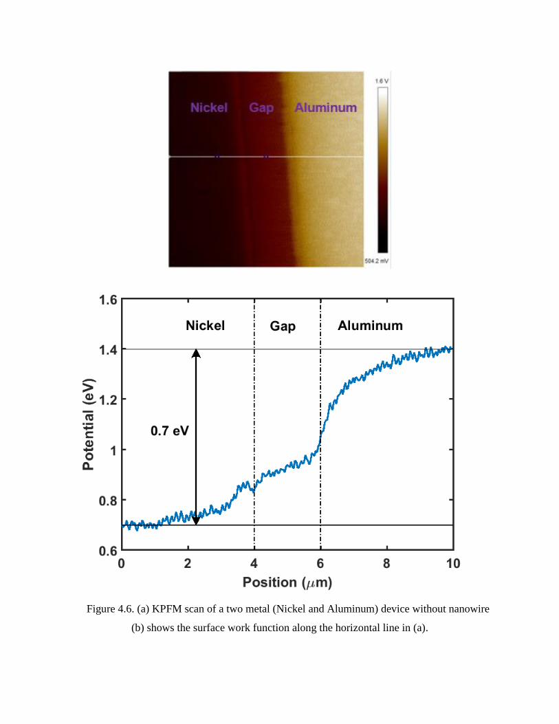
Figure 4.6. (a) KPFM scan of a two metal (Nickel and Aluminum) device without nanowire
(b) shows the surface work function along the horizontal line in (a).

4.3.4 Discussions
To present some plausible explanations for the measured electrical characteristics, we take a
bottom-up approach and consider the energy band diagrams for two different but simple current
channels, shown in Figure 4.7. In the first case, shown in Figure 4.7(a), there is only a single NW
between the two dissimilar work-function metals. The work function difference might induce band
banding[101], but the exact degree of band bending will depend on the NW, the two metals and
the two NW-metal contacts. Such bending can separate the photo-generated electrons and holes
and generate a photocurrent. The amount of the current will also depend on the characteristics of
the NW, the metal and the NW-metal contacts.
Figure 4.7. Energy band diagrams of current path for a single NW (a), and multiple NWs (b).
Figure 4.7(b) depicts the second case, in which a single current channel has two NWs instead
of one. In addition to factors in the first case, i.e., the NW, the metals and the NW-metal contacts,
the NW-NW interface will have some effect on channel conductivity. The barriers at the middle
of the energy bands represent non-ideal NW-NW interface due to presence of a nonconductive

shell or native oxide at the NW surface or a surface depletion layer. Such a barrier can make the
NW-NW interface the dominating factor and significantly reduce the channel conductivity.
Obviously as the number of NWs involved in a single current channel increases, the number of
NW-NW interfaces also increases and the current decrease might become more severe.
Depending on length and network density, dispersed NWs can be found in various possible
orientations, and their conduction can be dominated by single or multiple NW channels.
(i) If the NWs are sufficiently long and sparse, they can contact bothelectrodes directly,
as shown in Figure 4.8(a). Therefore, the sparse newtork will effectively consist of
many single-NW channels, such as the one in Figure 4.7(a) and lead to enhanced carrier
conduction and greater current.
(ii) The shorter NWs (i.e., shorter than the metal-to-metal gap) cannot individually contact
both electrodes, and they can only interlink to bridge the electrode gap and form a
device (cf. electrical percolation), as seen in Figure 4.8(b). In this case, the current
channels are similar to the one in Figure 4.7(b). The carrier transport will be limited by
the large NW-to-NW juction resistance due to the presence of a non-conducting shell
or native oxide at the NW surface[116], [122]. Thus, the higher the density of NWs,
the better the interlink[119], [123], and the larger the current.
(iii) Irrespective of the length size, if the density of the NW network is higher than what is
required for a one-NW-layer thick surface coverage, many NWs at the top might not
contact either electrode. Rather, they will be in contact with the underlying NWs, which
might be in direct contact with at least one of the electrodes (Al or Ni), as seen in Figure
4.8(c). Additionally most of the bottom NWs are likely in contact with only electrode
at one end, while the other end of the NW is surrounded by other NWs, instead of

contacting the other electrode. This scenario will again lead to current paths similar to
the one in Figure 4.7(b). But, unlike case (ii), the current channels will involve more
and more NWs as the network density increases, and the current will decrease due to
increasingly inefficient NW-NW transport.
Figure 4.8. RDNW device schematics. (a) long sparse NW network (inset shows band structure of a
Ni-NW-Al channel), (b) short, sparse NW network (inset shows band structure of a Ni-NW1-Oxide-NW2-
Al channel), (c) long, dense NW network, inset shows zoom in on one end of some of the top NWs.
Therefore, in the dark, the sparse (and sufficientlylong) NWs produce more current due to
better contact with the metal electrodes. When illuminated, the sparse NWs absorb photons directly
and transport carriers effectively, thereby exhibiting higher photocurrents. However, in the denser
NWs, the network is thick and most of the incident light is absorbed by the top NWs[124]. The

photogenerated carriers inside these NWs need to be transported through other NWs to the
electrode, and therefore, the NW-NW junction resistance limits the current flow, leading to smaller
current values in dense NW devices. This phenomenon is a result of inefficient nanoscale transport.
4.4 CONCLUSIONS
In summary, Ge- and SiNW-based low-cost randomly dispersed networks were fabricated and
their potential for self-powered photo-switching has been demonstrated. These devices can
efficiently trap and absorb the incident light and collect the photo generated excitons, as evidenced
by photocurrent measurements. Larger currents can be extracted from GeNWs than from SiNWs.
GeNW devices exhibit better photo-switching because of greater conductivity and inter-NW
transport. KPFM measurement suggests that contact work function difference of 0.7 eV is
achievable with Ni and Al. The ‘anomalous’ increase in current as the density of the randomly
dispersed NW networks decreases, when the electrode gap is comparable to the NW lengths, is a
general phenomenon of the devices tested and has been clearly explained. The consistency of the
results indicates that this anomaly is applicable to nanoscale devices with electrodes of either
similar or dissimilar work function and that there is an optimum number of dispersed NWs for
obtaining the best optoelectronic response

Chapter 5. STUDY OF NARROW AND BENT SILICON
NANOWIRES
Bent narrow silicon nanowires are studied using molecular dynamics and quantum mechanical
simulations. Details of nanowire bending process, electronic Hamiltonian generation, and
electronic transport calculation are covered. Local strain or strain in the atomic scale in nanowires
are analyzed, and electronic transport as well as the energy gap in the transport as a function of
bending strain and nanowire diameter is calculated. In addition, the simulation process is repeated
for the same nanowires but with uniaxial strain instead of bending. Comparison shows that for the
same nanowire and for the same amount of average strain, the decrease in energy gap in electronic
transmission is larger in the case of bending. This shows that, for the same range of strain variation,
a bent nanowire will absorb a wider spectrum of light than a uniaxially strained nanowire.
5.1 INTRODUCTION
Silicon nanowires have huge potential in micro- and nano-technology. They can be fabricated in
both top-down and bottom-up approaches, and have been employed in electronic devices (e.g.
nanotransistors [60], [61], [125], solar cells [1], [3], [11]), optoelectronic devices [126], sensors
[62], [63], [127], [128], as well as thermoelectric energy conversions [129], [130]. They have also
been fabricated in a range of diameters; from a few nanometers to a few hundred nanometers. The
sub-10nm diameter nanowires are particularly interesting, as unlike the bulk silicon and the wider
wires, they have been predicted to have a direct bandgap [28]–[30]. They are, thus, appropriate for
optoelectronic studies. More interestingly, the bandgap of the narrow silicon nanowires can be
changed through application of mechanical strain [30], [131]. It has also been shown that by
applying strain the direct bandgap of a narrow silicon nanowire can be turned into indirect, and

vice versa [28], [30]. As we know, direct bandgap semiconductor absorbs / emits light more
efficiently than indirect bandgap semiconductor. This means mechanical strain is important in
modulating both electronic and optoelectronic properties of narrow silicon nanowires.
Strain has traditionally been applied to planar MOSFETs to enhance their mobility [43]. The usual
approach to straining such devices is through lattice mismatch and stress-memorization [132]–
[134] techniques. For nanowires though, mechanical bending of the substrate containing the
nanowires [44], [45] or deposition of extra layer of straining materials [135], such oxide and
nitride, on a portion of the wire surface are common.
Simulation of different device phenomena is an integral part of research and development. It
is more important for nanodevices as most of the traditional theory is inadequate, and the
experimental studies are costly. Simulation and modeling help understand experiments, and can
also help devise new tests. Electronic simulations of nanodevices under strain has been done
mostly in the density functional theory (DFT) formalism [131], [136], which is the best approach
available. But DFT suffers from high computational demand. Because of this, almost all the atomic
level electronic property studies have been done only for uniaxial strain. To the best of our
knowledge, there has been no simulation works of bent silicon nanowires to study the effect of
bending strain on electronic properties. The reason might be that, due to the bent nature of the
nanowire, there is no crystal symmetry present. Without such a symmetry, the predominantly used
periodic boundary condition is not applicable along the length of the nanowire. So, as a
considerably long length of the bent nanowire needs to be studied, the computational demand is
huge.
For such large structures, classical molecular mechanics or dynamics (MD) study may be the
required compromise. It is atomistic so that atomic interactions will be accurately captured. But it

is also classical so that quantum effects will not be properly taken into account. More importantly,
its computational demand is less than that of DFT. Classical MD is extensively used in the study
of mechanical [137], [138] and thermal [139], [140] properties of many micro [141] and
nanodevices [142], [143], including silicon nanowires [140], [144]. Guenole et al. [145] used MD
to study the effect of temperature and surface states on plasticity in silicon nanowires, while Yang
et al. [146] studied the effects of the shape on the yield stresses of silicon nanowires. Cai et al.
[147] simulated nanowire size, and temperature effects, on its fracture mechanisms. Thermal
properties of silicon nanowires are crucial to the integration of nanowires in MEMS and NEMS
systems [148]–[150]. Silicon nanowire thermal conductivity was studied by non-equilibrium
molecular dynamics (NEMD) simulations in [151], while Aluru et al. [152] studied the size and
surface orientation effects on the thermal expansion coefficients. MD has been also used in the
study of properties of silicon nanoparticles [153], [154]. In reference [155], Andriotis et al. studied
electrical conductivity of tetrahedral and clathrate (or cagelike) nanowires. In many of these
simulations, MD and energy minimization have been used to extend, compress, or bend the
nanowires, and to extract information about their mechanical and thermal properties. But few have
studied the electronic properties [155] to a great detail, especially for the bent nanowires.
Although the studies of strain dependent electronic property of nanowires have exclusively
focused on uniaxial strain, real nanowires have some inherent bending present in them. They can
also be bent easily. Bottom up synthesized nanowires are usually not perfectly straight, rather they
are twisted as well as jumbled [31], [32]. In reference [33], Bertagnolli grew wires with a
predefined rectangular shape. Zhu et al. [34] demonstrated over 40% bending strain in nanowires
with tungsten tip. They could also make the bending permanent with low electron beam exposure.
In an ultimate bending strengths experiment, Cook et al. [35] bent silicon nanowires lying on a flat

substrate through sequential atomic force microscope (AFM) tip manipulations. They could
achieve a U-shape bending, and found that, as nanowire diameter decreased, the bending strength
increased. This means that very narrow nanowires, in addition to having quantum mechanical
properties, are stable even under large stress. Although these bending studies have been done
mostly on bottom up nanowires, even top-down fabricated nanowires can be bent intentionally
[36], [37] or unintentionally [38], [39]. Nannini et al. [38] demonstrated bending in released silicon
nanowires due to surface relaxation, and noticed that, an applied force can modify the mechanical
equilibrium. Moreover, top down and bottom up approaches can be combined [40] to get
horizontally suspended, well-oriented and size-controlled nanowire arrays. These new bending
approaches may open up new possibilities, and thus, electronic study of bent wires is necessary. It
is also informative to compare bent nanowires with uniaxially strained nanowires to get an idea
about their relative merits.
5.2 DESCRIPTION
This section presents detailed description about shape and size of the simulated nanowires, the
simulation approaches, and the bending as well as uniaxial straining method. Definition of strain
under the bent condition, the passivation approach as well as the electronic Hamiltonian generation
procedure are also discussed. Moreover, formalism for calculating electronic transmission of the
nanowire is briefly described.
5.2.1 Nanowire size and shape
Silicon nanowires with six different cross sectional areas are studied in this work. All the
nanowires are <110> directed, since experimentally it has been found that the smallest nanowires
grow mainly along the <110> direction [32], [156]–[160]. The average diameters of the nanowires

are 1.0 nm, 1.7 nm, 2.3 nm, 3.1 nm, 3.6 nm and 4.3 nm, which are labeled here as <110>2d,
<110>3d, <110>4d, <110>5d, <110>6d and <110>7d, respectively. The left side of Figure 5.1(a)
shows the hexagonal cross section of nanowire <110>3d; other nanowires have similar shape, but
they have either narrower or wider diameters. The right side of Figure 5.1(a) shows the assumed
co-ordinate system. The top of Figure 5.1(b) shows the full length of the nanowire in Figure 5.1(a)
while the bottom again shows the co-ordinate system. The total length of each nanowire is 19.922
nm, and there are 103 atomic layers along the length. Figure 5.1 (c) show three consecutive layers.
The starting nanowire structures were generated by the repetition of DFT optimized, unit cell sized
silicon nanowires studied in [30].

Figure 5.1. Nanowire cross section (a), length (b), a few layers along length (c).
(a)
(b)
(c)

5.2.2 Molecular dynamics
The molecular dynamics simulation is done with the Large-scale Atomic/Molecular Massively
Parallel Simulator (LAMMPS) [161]. The Tersoff [162], [163] many-body bond-order reactive
potential is used to describe the Si-Si interatomic interactions. Tersoff potential has been used in
the theoretical study of atomic structure and mechanical properties of branched silicon nanowires
[164], in the investigation of atomic elastic stiffness in silicon [165], and in the study of
mechanical properties of silicon nanowire under uniaxial tension and compression [166]. In
reference [167], Tersoff potential was used to study the effects of vacancy defects on thermal
conduction of silicon nanowires. It has also been concluded, from the prediction of bulk silicon
thermal conductivity, that Tersoff potential gives the best results for isotopically pure silicon [168].
Reference [169] concluded that Tersoff potential reasonably reproduced small defect clusters
predicted by the more comprehensive tight-binding or first-principles calculations. It should be
noted here that during our mechanical straining (bending as well as uniaxial strain) of the
nanowires, hydrogen passivation of nanowire surfaces was not included as potential for Si-H bond
is not available. In [167], it has been found that DFT calculations with or without hydrogen
passivation gave almost the same thermal conductance.
5.2.3 Procedure of applying bending and uniaxial strain
The nanowire is strained using the following procedure. The nanowire structure is first optimized
by using energy minimization, with no velocity or force restrictions on any atoms. Then, the atoms
are subdivided into three groups: the leftmost 8 atomic layers form the left group, the rightmost 8
atomic layers form the right group, and the rest fall in the middle group. To apply bending strain
to the middle group, first the atoms in the left (right) group are rotated counter clockwise

(clockwise) in the yz plane (Figure 5.1(b) top) by an angle of 0.05 degree. Then they are kept
frozen while energy minimization is done to the middle group of atoms. Similar approach for
bending nanowires was applied in mechanical study of silicon carbide nanowires [137]. After the
minimization, the atomic positions of all the atoms are saved, and the process is repeated for the
next increment of the rotation angle. To apply uniaxial strain to the middle group of atoms, instead
of rotating, the atoms in the left (right) group are shifted to the left (right) by 0.005 nm. The rest
of the minimization procedure is similar to bending.
5.2.4 Strain definition
For uniaxial strain, each atomic layer is under the same amount of strain, which is defined as
0
0
L L
L
where ε is the uniaxial strain, and 0L and L , respectively, are the layer-to-layer distances before
and after applying strain.
The strain profile along the length of a bent nanowire is nonlinear, that is, it changes from
layer to layer. For the bending approach described above, usually the bottom surface is compressed
while the top surface is under tensile strain. For purposes of calculation as well as for comparison
with the uniaxial case, a simplified strain definition is used. First, the average xyz positions of
each atomic layer, both before and after bending, are calculated. Then the strain between any two
consecutive layers is given by,
0
0
L L
L
(5.1)
where ε is the average strain, and 0L and L , respectively, are the average layer-to-layer distances
before and after the bending.

5.2.5 Cropping off nanowire ends
Since the left and right groups of atoms are kept fixed during the bending or uniaxial straining and
energy minimization process, the atoms in the middle group, which are close to atoms in the edge
groups, undergo some artificial deformations. To avoid such artificial deformation, the full length
of the bent nanowire is not used in the electronic calculations. Specifically, 19 layers of atoms
from each end (including those that are kept frozen during the minimization) are cropped off.
Electronic simulation is done using the remaining 65 layers of atoms. The cropping also decreases
the problem size making the NEGF calculation computationally a little less intensive. Even after
this cropping, however, the length is considerably larger than what is usually used in electronic
studies of nanowires under uniaxial strain.
5.2.6 Surface passivation
Next the nanowires after their ends cropped off are hydrogen passivated with the GaussView [170]
software. Although hydrogen passivation was not done during the energy minimization, it is
essential to do so before any electronic calculations. Otherwise, the dangling bonds at the
unpassivated nanowire surface will show up as electronic states inside the bandgap and
overshadow the true energy gap. In reference [30], D. Shiri et al. studied strain dependent
electronic properties of hydrogen passivated silicon nanowires. B. Li et al. [171] used hydrogen
passivated nanowires to study the effects of size and shape on surface lattice constants of silicon
nanowires. Experimentally, in [172] hydrogen passivation was done to silicon nanowires before
functionalization with organic substituents. S. Kim et al. [173] showed improvement in MOSFET
performance by doing high pressure hydrogen annealing which reduced interface states at silicon

nanowire and oxide interface. T. Tezukal et al. [174] found that annealing of top-down fabricated
nanowires in hydrogen made the nanowire surface less rough.
5.2.7 Electronic Hamiltonians and their sizes
The mechanics simulation gives the atomic positions. After that, for electronic calculations, the
position information has to be represented in the form of a Hamiltonian matrix. Here we use the
sp3d5s* tight binding (TB) method with parameters from Jancu [175]. Because of non-uniform
strain along the nanowire, Bloch’s theorem cannot be used, and thus, the usual electronic band
structure cannot be calculated. Instead, we calculate electronic transmission to find the energy gap
in it. Two types of Hamiltonians are generated: (i) in-layer Hamiltonian, which represents all the
atoms in a layer, and (ii) layer-to-layer Hamiltonian, which gives coupling between the atoms in
consecutive layers. Depending on the diameter, each layer can have 12 to 147 silicon, and 8 to 28
hydrogen atoms. Without considering spin-orbit coupling in sp3d5s* TB, Hamiltonian size for each
silicon atom is 10x10, and that for each hydrogen atom is 1x1. Thus, the Hamiltonian size of each
layer is between 128x128 and 1498x1498. As already pointed out, we have a total of 65 layers.
Thus, while the narrower nanowires pose less challenge in terms of processor and memory
requirements, the wider ones are really computationally intensive.
5.2.8 Calculation of electronic transmission
The transmission through the nanowire is calculated using the Green’s function [176] formalism,
which is briefly described next. First, the retarded Green function, rG (E) , of the nanowire as a
function of energy E is calculated as
1
( )( ) ( )
r
r r
L R
G EEI H E E
(5.2)

where H represents the Hamiltonian of the nanowire, I is an identity matrix, ( ) ( )r
L R E is the self-
energy of the left (right) contact. H is block tri-diagonal in nature due to both the layered structure
of the device and the use of nearest-neighbor TB Hamiltonian. The contact self-energy represents
the connection strength between the nanowire and the contact, and it can be rigorously calculated
by first calculating the surface Green’s function of the contact. But this calculation is very time
consuming and a simpler approach works. We assume, for each contact, a broadening function, Γ
, of the form
( ) 0( ) EL R E I (5.3)
and then, calculate the self-energy as
( ) ( )( )2
r
L R L R
iE (5.4)
where 0E is a constant with unit of energy. We assume its value to be equal to 50 mEv. Once
rG (E) has been calculated, the electronic transmission can be found from
( ) ( ) ( ) ( ) ( )r a
L RT E tr E G E E G E (5.5)
Here, aG (E) represents the advanced Green function of the nanowire, which is found form the
transpose-conjugate of rG (E) . tr here means the trace of the matrix.
5.3 RESULTS AND DISCUSSION
5.3.1 Strain analysis
In this subsection, we analyze the strains in the nanowires. An average representation for the axial
strain, as given by Eqn. (5.1), is calculated for easy correlation with electronic properties and
comparison with uniaxial strain results. Figure 5.2 shows three bent nanowires, (a) <110>3d, (b)

<110>5d, and (c) <110>7d, with their local atomic strain along the length (z) direction visualized
as color variation. To obtain this strain configuration, the left and right atom groups of each
nanowire was rotated by 15o in the vertical (yz) plane (Figure 5.1(b)). The top side of each
nanowire is under tension while the bottom side is under compression. The corner atoms are under
the largest amount of strain due to rotation. Also for a fixed amount of rotation, as expected, the
range of strain variation (from most compressive to most tensile) increases with the nanowire
diameter. In addition, the largest tensile strain magnitude is always higher than the largest
compressive strain magnitude, for example, +3.7% vs -2.3% for nanowire <110>3d. This is due
to the atomic potentials resisting compression more than tension because as the atoms are brought
closer to each other beyond the no-strain minimum energy position the energy increases
exponentially.

Figure 5.2. Local strain along the z-direction (length) in 3 different nanowires as a color plot; (a)
<110>3d, (b) <110>5d, (c) <110>7d.
Figure 5.3 shows the local strain along x-direction while Figure 5.4 shows y-direction atomic
strain for the nanowires (a) <110>3d, (b) <110>5d, and (c) <110>7d. For both cases, top surface
is under compression while bottom surface is under tension, which is opposite to what we saw for
z-direction. So the atoms that are under tension along the length compresses in the cross-sectional
plane. Note as y-dimension is slightly larger than x, the range of y-strain is also larger.

Figure 5.3. Local strain along the x-direction in 3 different nanowires as a color plot; (a) <110>3d,
(b) <110>5d, (c) <110>7d.

Figure 5.4. Local strain along the y-direction in 3 different nanowires as a color plot; (a) <110>3d,
(b) <110>5d, (c) <110>7d.
We next consider local strain in uniaxially strained nanowires. Figure 5.5 shows the strain
along (a) z (length) direction, (b) x direction and (c) y direction uniaxially strained <110>5d
nanowire. As expected, variation in strain along the length is small and the atoms are always under
tension. Such variation is due to fixing the end atoms and allowing the middle atoms to relax.
Strain along x and y directions are always compressive and again the range is larger along y since
the y dimension of the nanowire is also larger that x dimension.

Figure 5.5. Local strain along (a) z, (b) x, (c) y direction as a color plot for a uniaxially strained
<110>5d nanowire.
Next our goal is to get an average representation of the strain along the length in the bent
nanowires. Figure 5.6 plots all the three strain ranges (x-range (a), y-range (b), and z-range (c)) as
functions of the nanowire diameter for different amount of end atom group rotations. The ranges
are almost linearly proportion to the nanowire diameter. As already seen, the y-range values are
slightly higher than the x-range values as diameter along y is wider. Due to bending along the
length, z-range values are the largest.


Figure 5.6. Ranges of strain (x-range (a), y-range, (b) and z-range (c)) as functions of nanowire
diameter for different amount of end atom group rotations.
The strain plots in Figures 5.2, 5.3, 5.4 and 5.6 give an insight into strain profile of bent
nanowires, it is difficult to correlate them directly with the any electronic properties. For example,
it is not possible, for a specific nanowire under a specific amount of rotation, to show a one-to-one
relation between the strain value and electronic transmission as strain does not have single value.
Note that just the amount of rotation is not a good measure, especially if we want to make a
comparison with uniaxially strained nanowires. So some average strain value at each strain
configuration (or end atom rotation) is more convenient for such correlation. But any kind of
averaging will lose some information, and more importantly, such simplifications should be
justifiable. With such a goal in mind, we turn to the layer to layer strain of the nanowire.
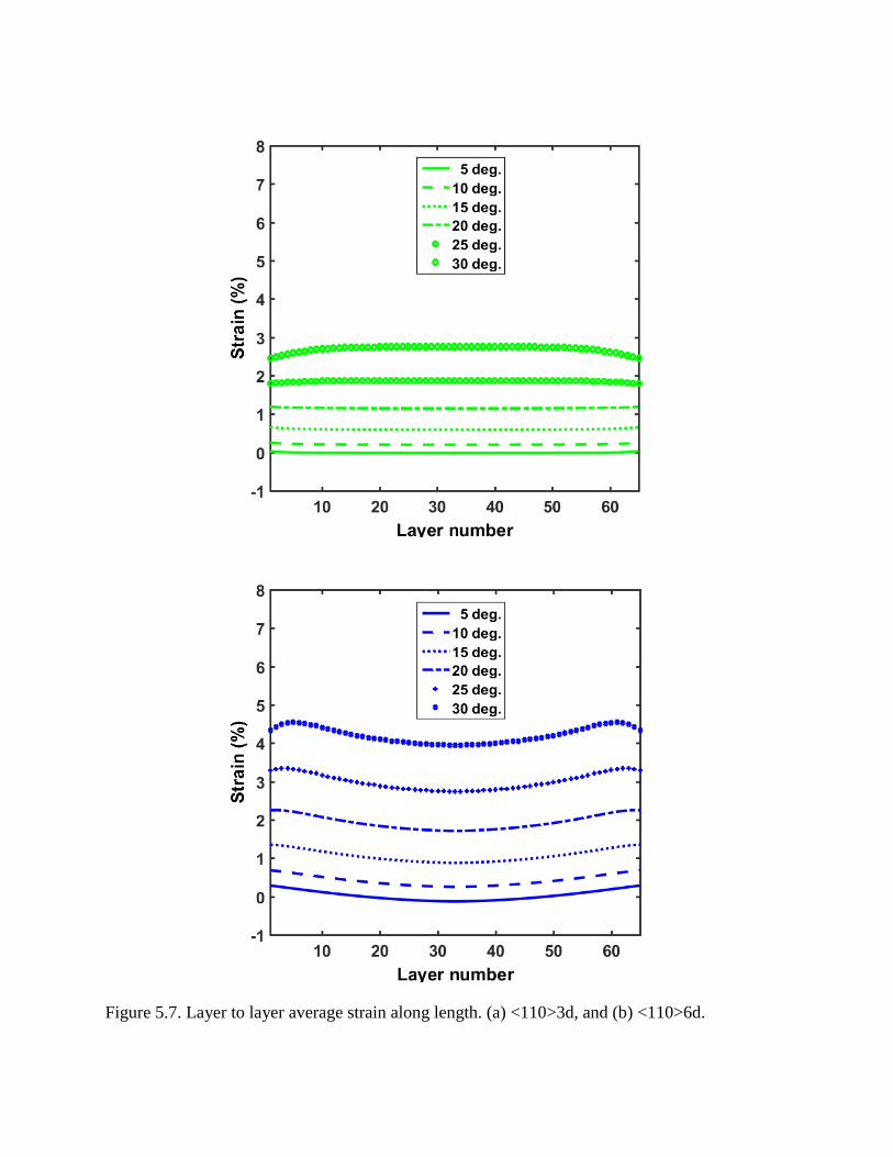
Figure 5.7. Layer to layer average strain along length. (a) <110>3d, and (b) <110>6d.
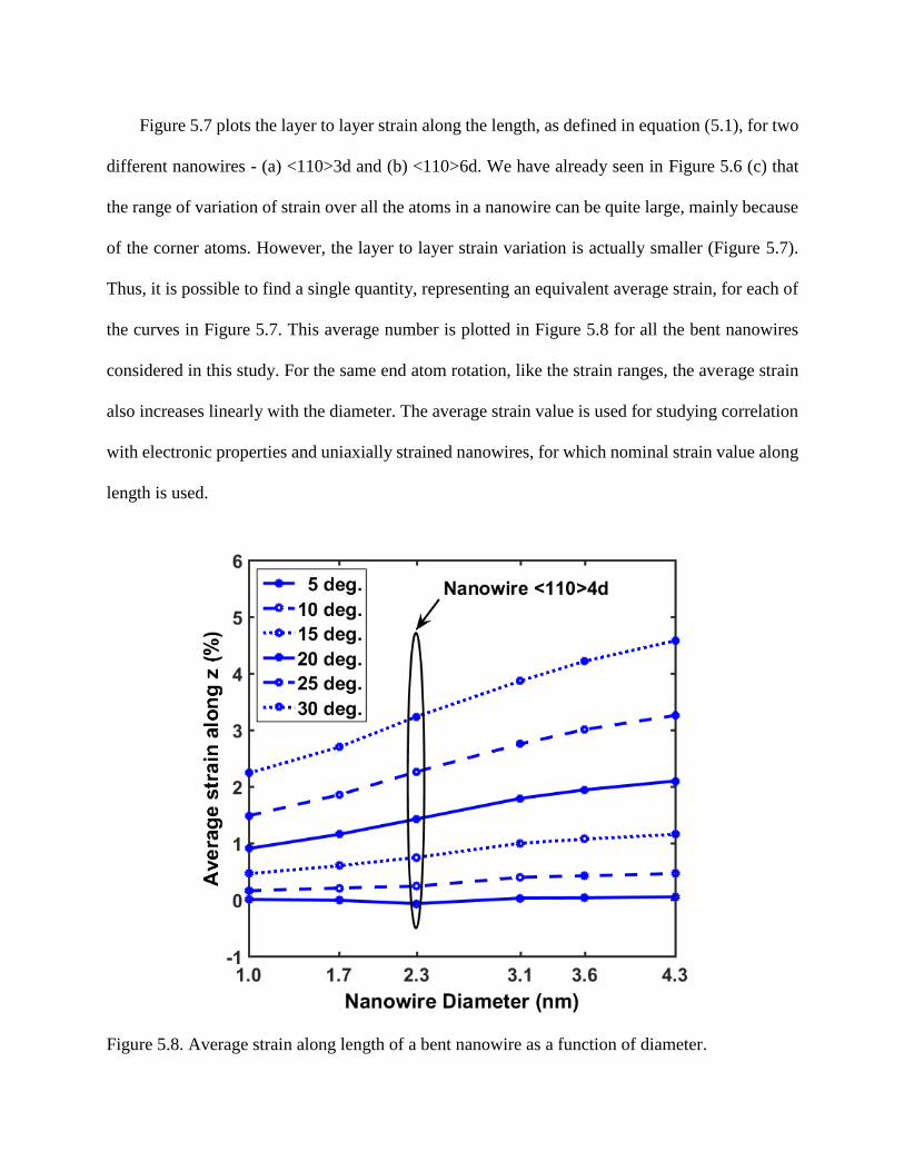
Figure 5.7 plots the layer to layer strain along the length, as defined in equation (5.1), for two
different nanowires - (a) <110>3d and (b) <110>6d. We have already seen in Figure 5.6 (c) that
the range of variation of strain over all the atoms in a nanowire can be quite large, mainly because
of the corner atoms. However, the layer to layer strain variation is actually smaller (Figure 5.7).
Thus, it is possible to find a single quantity, representing an equivalent average strain, for each of
the curves in Figure 5.7. This average number is plotted in Figure 5.8 for all the bent nanowires
considered in this study. For the same end atom rotation, like the strain ranges, the average strain
also increases linearly with the diameter. The average strain value is used for studying correlation
with electronic properties and uniaxially strained nanowires, for which nominal strain value along
length is used.
Figure 5.8. Average strain along length of a bent nanowire as a function of diameter.

5.3.2 Electronic transmission
Figure 5.9. Electronic transmission as a function of energy. (a) <110>2d with no rotation, (b)
<110>2d with 15-degree rotation, (c) <110>4d with no rotation, (d) <110>4d with 15-degree
rotation, (e) <110>6d with no rotation, (f) <110>6d with 15-degree rotation.
In bent nanowires, the bending strain compresses or extends the nanowire locally (Figures
5.2, 5.3 and 5.4), although on an average, the nanowire is under tensile strain along the length
(Figure 5.8). The strain (bending or uniaxial) changes the electronic band profile of the nanowire.
As already discussed, due to absence of any crystal symmetry under bending, it is not possible,

however, to calculate the energy band diagram using the Bloch’s theorem. We rather calculate the
electronic transmission (Eq. (5.5)) in the strained nanowires as a function of energy.
Figure 5.9 plots the electronic transmission as a function of energy for, respectively, zero and
15-degree end atom group rotations in the nanowires: (a, b) <110>2d, (c, d) <110>4d, (e, f)
<110>6d. We notice at least three important trends in the plots. First, a narrower nanowire has a
lower transmission value. A narrower nanowire has a fewer number of electronic modes, and at
any energy, transmission is proportional to the number of modes. So this is reasonable. Second,
the transmission gap - the continuous energy range over which the transmission is zero - in the
nanowire is larger than the bulk silicon bandgap. The transmission gap also decreases as the
nanowire diameter increases. This is expected since, in the limit of a very wide wire approaching
the bulk material, the energy gap in the wire should approach that in the bulk. Also it is to be
noticed that gaps in the unstrained nanowires - 2.43 eV (Figure 5.9(a)), 1.64 eV (Figure 5.9(c)),
and 1.47 eV (Figure 5.6(e)) - are consistent with both DFT [30] and DFTB [29] calculations. This
validates use of molecular dynamics for structure minimization. Third and most importantly, the
gap in each nanowire decreases as the amount of bending strain (that is, average strain along
length) increases. This behavior is also consistent with the results in [30], which predicts that for
an increase in uniaxial tensile strain in the nanowire, its bandgap decreases.
We can get a more comprehensive overview by studying the transmission energy gap as a
function of the nanowire diameter with the angle of end atom group rotation as a parameter. Such
characteristics are plotted in Figure 5.10 for no rotation and six different rotations (5, 10, 15, 20,
25, and 30 degree) conditions. We note that, the larger the nanowire diameter, the smaller the
transmission gap, which we already saw in Figure 5.9. For low bending strain (top curves), as the
nanowire diameter decreases from the largest diameter, 4.3 nm, the gap increases gradually. This

increase, however, becomes sharper as the diameter decreases below 1.7 nm. For large bending
strain (bottom curves), the gap increases rapidly in an almost linear fashion as the diameter
decreases. It is interesting to note that for the two widest wires, diameters 3.6 nm and 4.3 nm, the
gap completely disappears for larger strains. The reason for the disappearance of the gap is as
follows. We have seen, in Figure 5.6, that the strain range is higher for the wider wires. This means,
for large rotations, the local strains (both tensile and compression) in some parts of the wider wires
are very high (and of opposite direction). These large local strains represent a huge departure from
the perfect crystal structure and introduce many electronic modes in the band gap, thereby making
the gap totally disappear.
Figure 5.10. Transmission gap as a function of nanowire diameter for different rotation angles.

5.3.3 Bent nanowire vs. uniaxially strained nanowire
Figure 5.11 plots the energy gap in electronic transmission as a function of percentage strain for
six nanowires for both bent and uniaxially strained cases. Nanowire diameter increases as we go
from the top of the plot towards the bottom. The gap decreases linearly with the strain for both
method of straining. However, for the same diameter and the same average strain, the gap is
smaller and its decrease rate is faster in bent nanowire. Such trends have important consequences.
Smaller gap means the bent nanowires will have higher conductivity. The larger decrease rate also
means that the strain modulated band gap will respond to electromagnetic wave (light) of a wider
wavelength range. This clearly is an advantage of the bent nanowire over the uniaxially strained
nanowire.
Figure 5.11. Transmission gap as a function of % strain. Solid: bent, dashed: uniaxial.

Change in both conduction band minimum (Ec) and valence band maximum (Ev) can
contribute to the change in the gap. So it is informative to know which one contributes more.
Figure 5.12 plots both Ec and Ev for the cases in Figure 5.11. For narrow nanowires, both Ec and
Ev change at a similar rate, but as nanowire diameter increases, the Ev change becomes larger and
larger.
Figure 5.12. Ec and EV as a function of % strain. Solid: bent, dashed: uniaxial.

5.4 CONCLUSION
Atomic strain analysis and electronic transport calculation were done for six different nanowires
of varying diameters. Both bending strain and uniaxial strain have been considered. The whole
simulation process was described in detail. For the same amount of end atom rotation, the wider
the nanowire, the larger is the strain. This directly translates into smaller energy gaps in electronic
transmission for wider wires. Comparison of bent and uniaxially strained nanowire of same
diameter reveals that for same average strain the bent nanowire has a smaller gap in transmission.
The gap decrease rate is also found to be faster in the bent case. This makes bent nanowires superior
over uniaxially strained nanowires in terms of conductivity as well as strain modulated photo
absorption a wider wavelength range.

Chapter 6. SUMMARY AND FUTURE WORKS
This thesis explored modeling, fabrication and characterization of contact asymmetry (in size and
work function) effect on photoresponse of bulk silicon and nanowires of both silicon and
germanium semiconductors. It also investigated strain dependent electronic transport modulation
of narrow silicon nanowires. The main contributions of this work are summarized below:
1) In Chapter 2, we presented the theory of contact size asymmetry based photosensor.
If one contact has a larger area than the other, then under uniform illumination, the
device is asymmetric and produce large photocurrent at zero applied bias. Even for
symmetric contact devices asymmetry is possible if the light spot size is smaller
than contact to contact distance and the light is at an asymmetric point with respect
to the contacts. The theory was tested with prototype devices fabricated using a
single metal deposition process. Hundreds of zero bias photocurrent was achieved
and the response was fast and stable. Device simulation was also carried out to
further understand the underlying physics of such devices. It was found that contact
surface recombination and Schottky effects are essential for matching trends in
experimental I-V characteristics.
2) Chapter 3 discussed detailed modeling of single silicon wire solar cells. Symmetric
area contact with large work function difference (> 1 eV) can achieve performance
of p-n junction type solar cells without the need for controlled high doping in
nanowire devices. It was shown that due to recombination of photo generated
minority carriers with majority carriers, the short circuit current as well as open
circuit voltage saturates as nanowire length increases. The saturation length was
found to be approximately five times the diffusion length. With one contact metal

work function above and the second contact metal work function below the
nanowire work function, the first contact is Schottky while the other is Ohmic. The
Schottky metal work function has a large impact on both ISC and VOC than the
Ohmic contact.
Due to saturation, the current density performance of long nanowires worse than
short nanowires. We presented multiple contact design to boost the short circuit
current performance of the long wires without affecting the open circuit voltage.
We further studied grounded gate design for improving both ISC and VOC. Such
design also generates negative differential resistance effect in a non-resonant
tunneling device.
3) In Chapter 4, we described fabrication and characterization of nanowire network
based photo sensing devices with dual work function metal contacts. A process for
fabricating nanowire network with controlled density was developed. Our
characterization showed that the network produces appreciable photo response and
demonstrated, for the first time for visual wavelength, zero bias photo response in
nanowire network devices.
For devices with contact to contact distance larger than the nanowire length, the
higher the nanowire density the larger the current. However, for devices with metal
to metal distance shorter than nanowire length, sparser devices gave larger current
than that given by a considerably denser device. This behavior was explained by
considering the nanowire to nanowire transport phenomenon as our nanowires had
some less-conducting shell surrounding them. The shell act as a bottleneck in the
overall transport from one contact to the other. We also did KPFM measurements
to show that our contact metal pair achieved a work function difference of about
0.7 eV which generates the required asymmetry for large zero bias photocurrent.
4) Simulation work of strained narrow silicon nanowires with an emphasis on bent
nanowires was detailed in Chapter 5. The complete simulation methodology was
described and local (atomic) strain was analyzed as function of nanowire diameter,
direction as well as straining method (bending or uniaxial straining). Local strain
in bent nanowires varied widely in magnitude and direction (tensile vs
compressive). For comparison with uniaxial case, average strain along the length
was defined and it was found that as a function of diameter the average strain
increased linearly for same amount of end atom rotation used to cause bending.
Electronic transmission vs energy plot shows that the energy gap decreases as
diameter increases. For the same nanowire, the gap again decreases as the strain
increases. Comparison with uniaxially strained nanowires reveal that the decrease
rate is faster in bent nanowire for similar strain along the length. For nanowires
with diameters 3.6 nm and 4.3 nm, less than 5% strain is required to reduce the gap
to zero and cause a semiconductor to metal transition. Such transition is difficult, if
not impossible, to achieve in uniaxially strained nanowires due to the slow rate of
gap decrease with increase in strain. Since in bent nanowires, the range of strain
over all the atoms in a nanowire is large, achieving larger gap decrease rate seems
easier.
Below we briefly describe ways of extending this work:
1) The asymmetric contact area bulk silicon photosensor device work can be extended
by fabricating and characterizing devices with ranges of contact size, contact to

contact distance, and metals with a range of work functions. Our prototype devices
proved the theory and modeling indicated that surface recombination and barrier
lowering are important. But for finding the best device, the elaborate fabrication
and comparison with commercially available devices will be useful.
2) We did detailed modeling of single nanowire solar cell (or photo sensor) devices of
two or more contacts in Chapter 3. Top-down fabrication with SOI wafers can be
done to make such devices and characterize their performance against simulation
result. We studied nanowire network based photo sensor devices in Chapter 4. Our
KPFM measurement showed that our chosen metals Al and Ni had a work function
difference of about 0.7 eV. However, due to instrument limitation, we did not do
KPFM measurement on single nanowire devices. So fabrication of single nanowire
devices and doing KPFM to extract the complete KPFM profile from first metal to
nanowire to second contact would give valuable information about the band
structure of the device.
Energy gap measurement in narrow bent silicon nanowires can be done to complement our
simulation work of bent (as well as uniaxially strained) nanowires. Strain dependent photo
absorption / emission measurements can be done for such purposes.

BIBLIOGRAPHY
[1] L. Tsakalakos, J. Balch, J. Fronheiser, B. a. Korevaar, O. Sulima, and J. Rand, “Silicon
nanowire solar cells,” Appl. Phys. Lett., vol. 91, no. 23, p. 233117, 2007.
[2] V. Sivakov, G. Andrä, A. Gawlik, A. Berger, J. Plentz, F. Falk, and S. H. Christiansen,
“Silicon Nanowire-Based Solar Cells on Glass : Synthesis , Optical Properties , and Cell
Parameters,” Nano Lett., vol. 9, no. 4, pp. 1549–1554, 2009.
[3] E. Garnett and P. Yang, “Light trapping in silicon nanowire solar cells,” Nano Lett., vol.
10, no. 3, pp. 1082–1087, Mar. 2010.
[4] J. Li, H. Yu, S. M. Wong, X. Li, G. Zhang, P. G.-Q. Lo, and D.-L. Kwong, “Design
guidelines of periodic Si nanowire arrays for solar cell application,” Appl. Phys. Lett., vol.
95, no. 24, p. 243113, 2009.
[5] C. Lin and M. L. Povinelli, “Optical absorption enhancement in silicon nanowire arrays
with a large lattice constant for photovoltaic applications.,” Opt. Express, vol. 17, no. 22,
pp. 19371–81, Oct. 2009.
[6] M. M. Adachi, A. J. Labelle, S. M. Thon, X. Lan, S. Hoogland, and E. H. Sargent,
“Broadband solar absorption enhancement via periodic nanostructuring of electrodes,”
Sci. Rep., vol. 3, p. 2928, Jan. 2013.
[7] C. Yang, C. J. Barrelet, F. Capasso, and C. M. Lieber, “Single p-type/intrinsic/n-type
silicon nanowires as nanoscale avalanche photodetectors.,” Nano Lett., vol. 6, no. 12, pp.
2929–34, Dec. 2006.
[8] P. Servati, a. Colli, S. Hofmann, Y. Q. Fu, P. Beecher, Z. a. K. Durrani, a. C. Ferrari, a.
J. Flewitt, J. Robertson, and W. I. Milne, “Scalable silicon nanowire photodetectors,”
Phys. E Low-dimensional Syst. Nanostructures, vol. 38, no. 1–2, pp. 64–66, Apr. 2007.
[9] C. B. Winkelmann, I. Ionica, X. Chevalier, G. Royal, C. Bucher, and V. Bouchiat,
“Optical switching of porphyrin-coated silicon nanowire field effect transistors.,” Nano
Lett., vol. 7, no. 6, pp. 1454–8, Jun. 2007.
[10] J. Bae, H. Kim, X.-M. Zhang, C. H. Dang, Y. Zhang, Y. J. Choi, A. Nurmikko, and Z. L.
Wang, “Si nanowire metal-insulator-semiconductor photodetectors as efficient light
harvesters.,” Nanotechnology, vol. 21, no. 9, p. 095502, Mar. 2010.
[11] M. M. Adachi, M. P. Anantram, and K. S. Karim, “Core-shell silicon nanowire solar
cells,” Sci. Rep., vol. 3, p. 1546, Jan. 2013.
[12] M. G. Nikolaides, S. Rauschenbach, S. Luber, K. Buchholz, M. Tornow, G. Abstreiter,
and A. R. Bausch, “Silicon-on insulator based thin-film resistor for chemical and
biological sensor applications.,” Chemphyschem, vol. 4, no. 10, pp. 1104–6, Oct. 2003.
[13] C. Yu, Q. Hao, S. Saha, L. Shi, X. Kong, and Z. L. Wang, “Integration of metal oxide
nanobelts with microsystems for nerve agent detection,” Appl. Phys. Lett., vol. 86, no. 6,
p. 063101, Jan. 2005.
[14] Z. Li, B. Rajendran, T. I. Kamins, X. Li, Y. Chen, and R. S. Williams, “Silicon nanowires
for sequence-specific DNA sensing: device fabrication and simulation,” Appl. Phys. A,
vol. 80, no. 6, pp. 1257–1263, Mar. 2005.
[15] A. Tibuzzi, B. Margesin, M. Decarli, C. DiNatale, M. Zen, A. D’Amico, and G. Soncini,
“MOS-Junction-Based Nanostructures by Thermal Oxidation of Silicon Wires for
Hydrogen Detection,” IEEE Trans. Nanotechnol., vol. 3, no. 2, pp. 287–292, Jun. 2004.
[16] D. Zhang, Z. Liu, C. Li, T. Tang, X. Liu, S. Han, B. Lei, and C. Zhou, “Detection of NO 2
down to ppb Levels Using Individual and Multiple In 2 O 3 Nanowire Devices,” Nano

Lett., vol. 4, no. 10, pp. 1919–1924, Oct. 2004.
[17] J. M. Lee and W. Lee, “Effects of Surface Roughness on Hydrogen Gas Sensing
Properties of Single Pd Nanowires.” American Scientific Publishers.
[18] F. Wang, S. Yip, N. Han, K. Fok, H. Lin, J. J. Hou, G. Dong, T. Hung, K. S. Chan, and J.
C. Ho, “Surface roughness induced electron mobility degradation in InAs nanowires.,”
Nanotechnology, vol. 24, no. 37, p. 375202, Sep. 2013.
[19] L. J. Lauhon, M. S. Gudiksen, D. Wang, and C. M. Lieber, “Epitaxial core-shell and core-
multishell nanowire heterostructures.,” Nature, vol. 420, no. 6911, pp. 57–61, Nov. 2002.
[20] Y. Dong, B. Tian, T. J. Kempa, and C. M. Lieber, “Coaxial group III-nitride nanowire
photovoltaics,” Nano Lett., vol. 9, no. 5, pp. 2183–7, May 2009.
[21] B. M. Kayes, H. a. Atwater, and N. S. Lewis, “Comparison of the device physics
principles of planar and radial p-n junction nanorod solar cells,” J. Appl. Phys., vol. 97,
no. 11, p. 114302, 2005.
[22] W. Shockley and H. J. Queisser, “Detailed Balance Limit of Efficiency of p-n Junction
Solar Cells,” J. Appl. Phys., vol. 32, no. 3, p. 510, 1961.
[23] E. C. Garnett and P. Yang, “Silicon nanowire radial p-n junction solar cells,” J. Am.
Chem. Soc., vol. 130, no. 29, pp. 9224–5, Jul. 2008.
[24] P. Peercy, “The drive to miniaturization,” Nature, vol. 406, no. 6799, pp. 1023–1026,
Aug. 2000.
[25] C. Claeys, “Technological Challenges of Advanced CMOS Processing and Their Impact
on Design Aspects,” Proc. 17th Int. Conf. VLSI Des., p. 275, 2004.
[26] S. Xiong and J. Bokor, “Structural Optimization of SUTBDG Devices for Low-Power
Applications,” IEEE Trans. Electron Devices, vol. 52, no. 3, pp. 360–366, Mar. 2005.
[27] E. C. Jones and E. Ishida, “Shallow junction doping technologies for ULSI,” Mater. Sci.
Eng. R Reports, vol. 24, no. 1–2, pp. 1–80, 1998.
[28] X. B. Yang and R. Q. Zhang, “Indirect-to-direct band gap transitions in phosphorus
adsorbed ⟨112⟩ silicon nanowires,” Appl. Phys. Lett., vol. 93, no. 17, p. 173108, 2008.
[29] M. Nolan, S. O’Callaghan, G. Fagas, J. C. Greer, and T. Frauenheim, “Silicon nanowire
band gap modification.,” Nano Lett., vol. 7, no. 1, pp. 34–8, Jan. 2007.
[30] D. Shiri, Y. Kong, A. Buin, and M. P. Anantram, “Strain induced change of bandgap and
effective mass in silicon nanowires,” Appl. Phys. Lett., vol. 93, no. 7, p. 073114, 2008.
[31] S. Hofmann, C. Ducati, R. J. Neill, S. Piscanec, a. C. Ferrari, J. Geng, R. E. Dunin-
Borkowski, and J. Robertson, “Gold catalyzed growth of silicon nanowires by plasma
enhanced chemical vapor deposition,” J. Appl. Phys., vol. 94, no. 9, p. 6005, 2003.
[32] Y. Cui, L. J. Lauhon, M. S. Gudiksen, J. Wang, and C. M. Lieber, “Diameter-controlled
synthesis of single-crystal silicon nanowires,” Appl. Phys. Lett., vol. 78, no. 15, p. 2214,
2001.
[33] W. Molnar, a Lugstein, P. Pongratz, M. Seyring, M. Rettenmayr, C. Borschel, C.
Ronning, N. Auner, C. Bauch, and E. Bertagnolli, “A general approach toward shape-
controlled synthesis of silicon nanowires.,” Nano Lett., vol. 13, no. 1, pp. 21–5, Jan. 2013.
[34] S. Dai, J. Zhao, L. Xie, Y. Cai, N. Wang, and J. Zhu, “Electron-beam-induced elastic-
plastic transition in Si nanowires,” Nano Lett., vol. 12, no. 5, pp. 2379–85, May 2012.
[35] G. Stan, S. Krylyuk, a V Davydov, I. Levin, and R. F. Cook, “Ultimate bending strength
of Si nanowires.,” Nano Lett., vol. 12, no. 5, pp. 2599–604, May 2012.
[36] S. Zhang, L. Lou, and C. Lee, “Piezoresistive silicon nanowire based
nanoelectromechanical system cantilever air flow sensor,” Appl. Phys. Lett., vol. 100, no.

2, p. 023111, 2012.
[37] R. Yang, T. He, C. Marcoux, P. Andreucci, L. Duraffourg, P. X. Feng, E. Engineering, C.
Western, M. Campus, and G. Cedex, “SILICON NANOWIRE AND CANTILEVER
ELECTROMECHANICAL SWITCHES WITH INTEGRATED PIEZORESISTIVE
TRANSDUCERS,” pp. 1–4, 2013.
[38] G. Pennelli, M. Totaro, A. Nannini, U. Pisa, V. G. Caruso, and I.- Pisa, “Correlation
between Surface Stress and Apparent Young ’ s Modulus of Top-Down Silicon
Nanowires,” no. 12, pp. 10727–10734, 2012.
[39] M. G. Rabbani, “Unpublished,” 2011.
[40] A. S. Paulo, N. Arellano, J. a Plaza, R. He, C. Carraro, R. Maboudian, R. T. Howe, J.
Bokor, and P. Yang, “Suspended mechanical structures based on elastic silicon nanowire
arrays.,” Nano Lett., vol. 7, no. 4, pp. 1100–4, Apr. 2007.
[41] C. O. Chui, S. Member, A. K. Okyay, and K. C. Saraswat, “Effective Dark Current
Suppression With Asymmetric MSM Photodetectors in Group IV Semiconductors,” IEEE
PHOTONICS Technol. Lett., vol. 15, no. 11, pp. 1585–1587, 2003.
[42] T. Mizuno, S. Takagi, N. Sugiyama, H. Satake, a. Kurobe, and a. Toriumi, “Electron and
hole mobility enhancement in strained-Si MOSFET’s on SiGe-on-insulator substrates
fabricated by SIMOX technology,” IEEE Electron Device Lett., vol. 21, no. 5, pp. 230–
232, May 2000.
[43] S. E. Thompson, M. Armstrong, C. Auth, S. Cea, R. Chau, G. Glass, T. Hoffman, J.
Klaus, Z. Ma, B. Mcintyre, a. Murthy, B. Obradovic, L. Shifren, S. Sivakumar, S. Tyagi,
T. Ghani, K. Mistry, M. Bohr, and Y. El-Mansy, “A Logic Nanotechnology Featuring
Strained-Silicon,” IEEE Electron Device Lett., vol. 25, no. 4, pp. 191–193, Apr. 2004.
[44] R. He and P. Yang, “Giant piezoresistance effect in silicon nanowires,” Nat.
Nanotechnol., vol. 1, no. 1, pp. 42–6, Oct. 2006.
[45] E. F. Arkan, D. Sacchetto, I. Yildiz, Y. Leblebici, and B. E. Alaca, “Monolithic
integration of Si nanowires with metallic electrodes: NEMS resonator and switch
applications,” J. Micromechanics Microengineering, vol. 21, no. 12, p. 125018, Dec.
2011.
[46] B. Culshaw, “Optical fiber sensor technologies: opportunities and-perhaps-pitfalls,” J.
Light. Technol., vol. 22, no. 1, pp. 39–50, 2004.
[47] F. Prieto, B. Sep lveda, a Calle, a Llobera, C. Dom nguez, a Abad, a Montoya, and L.
M. Lechuga, “An integrated optical interferometric nanodevice based on silicon
technology for biosensor applications,” Nanotechnology, vol. 14, no. 8, pp. 907–912,
2003.
[48] S. P. Sundararajan, N. K. Grady, N. Mirin, and N. J. Halas, “Nanoparticle-induced
enhancement and suppression of photocurrent in a silicon photodiode,” Nano Lett., vol. 8,
no. 2, pp. 624–30, Feb. 2008.
[49] a. Nascetti and D. Caputo, “Amorphous silicon phototransistor as nonlinear optical device
for high dynamic range imagers,” IEEE Trans. Electron Devices, vol. 49, no. 3, pp. 395–
399, Mar. 2002.
[50] A. Zhang, S. You, C. Soci, Y. Liu, D. Wang, and Y.-H. Lo, “Silicon nanowire detectors
showing phototransistive gain,” Appl. Phys. Lett., vol. 93, no. 12, p. 121110, 2008.
[51] I. Goykhman, B. Desiatov, J. Khurgin, J. Shappir, and U. Levy, “Waveguide based
compact silicon Schottky photodetector with enhanced responsivity in the telecom spectral
band,” Opt. Express, vol. 20, no. 27, pp. 28594–602, Dec. 2012.

[52] M. Casalino, M. Iodice, L. Sirleto, I. Rendina, and G. Coppola, “Asymmetric MSM sub-
bandgap all-silicon photodetector with low dark current,” Opt. Express, vol. 21, no. 23,
pp. 28072–28082, 2013.
[53] A. K. Okyay, C. O. Chui, and K. C. Saraswat, “Leakage suppression by asymmetric area
electrodes in metal-semiconductor-metal photodetectors,” Appl. Phys. Lett., vol. 88, no. 6,
p. 063506, 2006.
[54] W. a. Wohlmuth, M. Arafa, A. Mahajan, P. Fay, and I. Adesida, “InGaAs metal-
semiconductor-metal photodetectors with engineered Schottky barrier heights,” Appl.
Phys. Lett., vol. 69, no. 23, p. 3578, 1996.
[55] S. Zhu, G. Q. Lo, and D. L. Kwong, “Low-Cost and High-Speed SOI Waveguide-Based
Silicide Schottky-Barrier MSM Photodetectors for Broadband Optical Communications,”
IEEE PHOTONICS Technol. Lett., vol. 20, no. 16, pp. 1396–1398, 2008.
[56] S. Zhu, M. B. Yu, G. Q. Lo, and D. L. Kwong, “Near-infrared waveguide-based nickel
silicide Schottky-barrier photodetector for optical communications,” Appl. Phys. Lett., vol.
92, no. 8, p. 081103, 2008.
[57] Z. Shiyu, H. Xia, F. Xu, and Y. Hui, “Design of Silicon Based Germanium Metal-
semiconductor-metal Photodetector with Asymmetric Area Electrodes,” Opto-electronic
Eng., vol. 42, no. 01, 2015.
[58] S. M. Sze, “Physics of Semiconductor Devices,” John Wiley Sons, Inc., no. second
edition, 1981.
[59] “Atlas, Silvaco. Available: http://www.silvaco.com,” 2014. [Online]. Available:
http://www.silvaco.com/.
[60] G. Larrieu and X.-L. Han, “Vertical nanowire array-based field effect transistors for
ultimate scaling,” Nanoscale, vol. 5, no. 6, pp. 2437–2441, Mar. 2013.
[61] J.-P. Colinge, C.-W. Lee, A. Afzalian, N. D. Akhavan, R. Yan, I. Ferain, P. Razavi, B.
O’Neill, A. Blake, M. White, A.-M. Kelleher, B. McCarthy, and R. Murphy, “Nanowire
transistors without junctions,” Nat. Nanotechnol., vol. 5, no. 3, pp. 225–229, Mar. 2010.
[62] I. Park, Z. Li, A. P. Pisano, and R. S. Williams, “Top-down fabricated silicon nanowire
sensors for real-time chemical detection,” Nanotechnology, vol. 21, no. 1, p. 015501, Jan.
2010.
[63] G. Zheng, F. Patolsky, Y. Cui, W. U. Wang, and C. M. Lieber, “Multiplexed electrical
detection of cancer markers with nanowire sensor arrays,” Nat. Biotechnol., vol. 23, no.
10, pp. 1294–1301, Oct. 2005.
[64] Y. Cui, J. Wang, S. R. Plissard, A. Cavalli, T. T. T. Vu, R. P. J. van Veldhoven, L. Gao,
M. Trainor, M. A. Verheijen, J. E. M. Haverkort, and E. P. A. M. Bakkers, “Efficiency
Enhancement of InP Nanowire Solar Sells by Surface Cleaning,” Nano Lett., vol. 13, no.
9, pp. 4113–4117, Sep. 2013.
[65] B. Tian, X. Zheng, T. J. Kempa, Y. Fang, N. Yu, G. Yu, J. Huang, and C. M. Lieber,
“Coaxial silicon nanowires as solar cells and nanoelectronic power sources,” Nature, vol.
449, no. 7164, pp. 885–890, Oct. 2007.
[66] J. Kim, J.-H. Yun, C.-S. Han, Y. J. Cho, J. Park, and Y. C. Park, “Multiple silicon
nanowires-embedded Schottky solar cell,” Appl. Phys. Lett., vol. 95, no. 14, p. 143112,
2009.
[67] M. D. Kelzenberg, D. B. Turner-Evans, B. M. Kayes, M. A. Filler, M. C. Putnam, N. S.
Lewis, and H. A. Atwater, “Photovoltaic measurements in single-nanowire silicon solar
cells,” Nano Lett., vol. 8, no. 2, pp. 710–714, Feb. 2008.

[68] F. Zhang, T. Song, and B. Sun, “Conjugated polymer-silicon nanowire array hybrid
Schottky diode for solar cell application,” Nanotechnology, vol. 23, no. 19, p. 194006,
May 2012.
[69] R. F. Pierret, Modular series on solid state devices: Volume I: Semiconductor
Fundamental. Addison-Wesley publishing company, 1983.
[70] J. a. del Alamo and R. M. Swanson, “Modelling of minority-carrier transport in heavily
doped silicon emitters,” Solid. State. Electron., vol. 30, no. 11, pp. 1127–1136, Nov. 1987.
[71] M. S. Tyagi and R. Van Overstraeten, “Minority carrier recombination in heavily-doped
silicon,” Solid. State. Electron., vol. 26, no. 6, pp. 577–597, Jun. 1983.
[72] J. E. Allen, E. R. Hemesath, D. E. Perea, J. L. Lensch-Falk, Z. Y. Li, F. Yin, M. H. Gass,
P. Wang, A. L. Bleloch, R. E. Palmer, and L. J. Lauhon, “High-resolution detection of Au
catalyst atoms in Si nanowires,” Nat. Nanotechnol., vol. 3, no. 3, pp. 168–173, Mar. 2008.
[73] Y. Jung, A. Vacic, D. E. Perea, S. T. Picraux, and M. a. Reed, “Minority Carrier Lifetimes
and Surface Effects in VLS-Grown Axial p-n Junction Silicon Nanowires,” Adv. Mater.,
vol. 23, no. 37, pp. 4306–4311, Oct. 2011.
[74] Y. Dan, K. Seo, K. Takei, J. H. Meza, A. Javey, and K. B. Crozier, “Dramatic reduction of
surface recombination by in situ surface passivation of silicon nanowires,” Nano Lett., vol.
11, no. 6, pp. 2527–2532, Jun. 2011.
[75] S. Kato, Y. Kurokawa, S. Miyajima, Y. Watanabe, A. Yamada, Y. Ohta, Y. Niwa, and M.
Hirota, “Improvement of carrier diffusion length in silicon nanowire arrays using atomic
layer deposition,” Nanoscale Res. Lett., vol. 8, no. 1, p. 361, Jan. 2013.
[76] H. Zimmermann and H. Ryssel, “Trivalent character of platinum in silicon,” Appl. Phys.
Lett., vol. 58, no. 5, p. 499, 1991.
[77] M. D. Miller, “Lifetime-controlling recombination centers in platinum-diffused silicon,” J.
Appl. Phys., vol. 47, no. 6, p. 2569, 1976.
[78] C. France, The Reactivity Series of Metals. Available: http://www.gcsescience.com/r1-
reactivity-series-metals.htm. 2014.
[79] M.-F. Ng, L. Y. Sim, H. Da, H. Jin, K. H. Lim, and S.-W. Yang, “Modulation of the work
function of silicon nanowire by chemical surface passivation: a DFT study,” Theor. Chem.
Acc., vol. 127, no. 5–6, pp. 689–695, Jul. 2010.
[80] T. C. Cheng, J. Shieh, W. J. Huang, M. C. Yang, M. H. Cheng, H. M. Lin, and M. N.
Chang, “Hydrogen plasma dry etching method for field emission application,” Appl. Phys.
Lett., vol. 88, no. 26, p. 263118, 2006.
[81] M. D. Kelzenberg, D. B. Turner-Evans, B. M. Kayes, M. a. Filler, M. C. Putnam, N. S.
Lewis, and H. a. Atwater, “Single-nanowire Si solar cells,” 2008 33rd IEEE Photovolatic
Spec. Conf., pp. 1–6, May 2008.
[82] T. Xu, Y. Lambert, C. Krzeminski, B. Grandidier, D. Stievenard, G. Leveque, A. Akjouj,
Y. Pennec, and B. Djafari-Rouhani, “Optical absorption of silicon nanowires,” J. Appl.
Phys., vol. 112, no. 3, p. 033506, 2012.
[83] L. Hu and G. Chen, “Analysis of optical absorption in silicon nanowire arrays for
photovoltaic applications,” Nano Lett., vol. 7, no. 11, pp. 3249–3252, Nov. 2007.
[84] S.-K. Kim, R. W. Day, J. F. Cahoon, T. J. Kempa, K.-D. Song, H.-G. Park, and C. M.
Lieber, “Tuning light absorption in core/shell silicon nanowire photovoltaic devices
through morphological design,” Nano Lett., vol. 12, no. 9, pp. 4971–4976, Sep. 2012.
[85] R. a. Sinton and A. Cuevas, “Contactless determination of current–voltage characteristics
and minority-carrier lifetimes in semiconductors from quasi-steady-state
photoconductance data,” Appl. Phys. Lett., vol. 69, no. 17, p. 2510, 1996.
[86] W. Il Park, G. Zheng, X. Jiang, B. Tian, and C. M. Lieber, “Controlled synthesis of
millimeter-long silicon nanowires with uniform electronic properties,” Nano Lett., vol. 8,
no. 9, pp. 3004–3009, Sep. 2008.
[87] B. W. Shi, H. Peng, Y. Zheng, N. Wang, N. Shang, Z. Pan, C. Lee, and S. Lee, “Synthesis
of Large Areas of Highly Oriented, Very Long Silicon Nanowires,” Adv. Mater., vol. 12,
no. 18, pp. 1343–1345, 2000.
[88] Y. Shi, Q. Hu, H. Araki, H. Suzuki, H. Gao, W. Yang, and T. Noda, “Long Si nanowires
with millimeter-scale length by modified thermal evaporation from Si powder,” Appl.
Phys. A, vol. 80, no. 8, pp. 1733–1736, Feb. 2004.
[89] Y. F. Zhang, Y. H. Tang, C. Lam, N. Wang, C. S. Lee, I. Bello, and S. T. Lee, “Bulk-
quantity Si nanowires synthesized by SiO sublimation,” J. Cryst. Growth, vol. 212, no. 1–
2, pp. 115–118, Jan. 2000.
[90] P. Yang, R. Yan, and M. Fardy, “Semiconductor Nanowire: What’s Next?,” Nano Lett.,
vol. 10, no. 5, pp. 1529–1536, 2010.
[91] R. Yan, D. Gargas, and P. Yang, “Nanowire photonics,” Nat. Photonics, vol. 3, no. 10, pp.
569–576, Oct. 2009.
[92] L. Zhang, X. Zhang, J. Lai, Z. Liu, S. Hou, S. Xie, and M. Gao, “Optically Powered ZnO
Nanowires with Symmetric and Asymmetric Contacts,” J. Nanosci. Nanotechnol., vol. 13,
no. 2, pp. 1203–1207, 2013.
[93] Y. Wu, H. Yan, M. Huang, B. Messer, J. H. Song, and P. Yang, “Inorganic Semiconductor
Nanowires: Rational Growth, Assembly, and Novel Properties,” Chem. – A Eur. J., vol. 8,
no. 6, pp. 1260–1268, 2002.
[94] C. M. Natarajan, M. G. Tanner, and R. H. Hadfield, “Superconducting nanowire single-
photon detectors: physics and applications,” Supercond. Sci. Technol., vol. 25, no. 6, p.
63001, 2012.
[95] H. Bao, W. Zhang, L. Chen, H. Huang, C. Yang, and X. Ruan, “An investigation of the
optical properties of disordered silicon nanowire mats,” J. Appl. Phys., vol. 112, no. 12, p.
124301, 2012.
[96] Y. Li, Q. Chen, D. He, and J. Li, “Radial junction Si micro/nano-wire array photovoltaics:
Recent progress from theoretical investigation to experimental realization,” Nano Energy,
vol. 7, pp. 10–24, 2014.
[97] V. C. Holmberg, T. D. Bogart, A. M. Chockla, C. M. Hessel, and B. A. Korgel, “Optical
Properties of Silicon and Germanium Nanowire Fabric,” J. Phys. Chem. C, vol. 116, pp.
22486–22491, 2012.
[98] F. Leonard and A. A. Talin, “Size-Dependent Effects on Electrical Contacts to Nanotubes
and Nanowires,” Phys. Rev. Lett., vol. 97, no. 2, p. 26804, Jul. 2006.
[99] E. Stern, G. Cheng, M. P. Young, and M. A. Reed, “Specific contact resistivity of
nanowire devices,” Appl. Phys. Lett., vol. 88, no. 5, p. 053106, 2006.
[100] Y.-F. Lin and W.-B. Jian, “The Impact of Nanocontact on Nanowire Based
Nanoelectronics,” Nano Lett., vol. 8, no. 10, pp. 3146–3150, 2008.
[101] M. G. Rabbani, A. Verma, M. M. Adachi, J. P. Sundararajan, M. M. Khader, R. Nekovei,
and M. P. Anantram, “Modeling of dual-metal Schottky contacts based silicon micro and
nano wire solar cells,” Sol. Energy Mater. Sol. Cells, vol. 130, pp. 456–465, 2014.
[102] L. Peng, L. Hu, and X. Fang, “Energy Harvesting for Nanostructured Self-Powered
Photodetectors,” Adv. Funct. Mater., vol. 24, no. 18, pp. 2591–2610, May 2014.

[103] K. Das, S. Samanta, P. Kumar, K. S. Narayan, and A. K. Raychaudhuri, “Fabrication of
Single Si Nanowire Metal–Semiconductor–Metal Device for Photodetection,” IEEE
Trans. Electron Devices, vol. 61, no. 5, pp. 1444–1450, May 2014.
[104] Z.-M. Liao, J. Xu, J.-M. Zhang, and D.-P. Yu, “Photovoltaic effect and charge storage in
single ZnO nanowires,” Appl. Phys. Lett., vol. 93, no. 2, p. 023111, 2008.
[105] Z. Bai, X. Yan, X. Chen, K. Zhao, P. Lin, and Y. Zhang, “High sensitivity, fast speed and
self-powered ultraviolet photodetectors based on ZnO micro/nanowire networks,” Prog.
Nat. Sci. Mater. Int., vol. 24, no. 1, pp. 1–5, Feb. 2014.
[106] T. I. Kamins, R. Stanley Williams, D. P. Basile, T. Hesjedal, and J. S. Harris, “Ti-
catalyzed Si nanowires by chemical vapor deposition: Microscopy and growth
mechanisms,” J. Appl. Phys., vol. 89, no. 2, p. 1008, Jan. 2001.
[107] A. M. Morales and C. M. Lieber, “A Laser Ablation Method for the Synthesis of
Crystalline Semiconductor Nanowires,” Science (80-. )., vol. 279, no. 5348, pp. 208–211,
Jan. 1998.
[108] X. Duan, J. Wang, and C. M. Lieber, “Synthesis and optical properties of gallium arsenide
nanowires,” Appl. Phys. Lett., vol. 76, no. 9, p. 1116, 2000.
[109] M. S. Gudiksen, J. Wang, and C. M. Lieber, “Synthetic Control of the Diameter and
Length of Single Crystal Semiconductor Nanowires,” J. Phys. Chem. B, vol. 105, no. 19,
pp. 4062–4064, May 2001.
[110] T. Hanrath and B. A. Korgel, “Supercritical Fluid–Liquid–Solid (SFLS) Synthesis of Si
and Ge Nanowires Seeded by Colloidal Metal Nanocrystals,” Adv. Mater., vol. 15, no. 5,
pp. 437–440, Mar. 2003.
[111] F. M. Davidson, R. Wiacek, and B. A. Korgel, “Supercritical Fluid−Liquid−Solid
Synthesis of Gallium Phosphide Nanowires,” Chem. Mater., vol. 17, no. 2, pp. 230–233,
Jan. 2005.
[112] F.-W. Yuan and H.-Y. Tuan, “Supercritical Fluid−Solid Growth of Single-Crystalline
Silicon Nanowires: An Example of Metal-Free Growth in an Organic Solvent,” Cryst.
Growth Des., vol. 10, no. 11, pp. 4741–4745, Nov. 2010.
[113] V. C. Holmberg and B. A. Korgel, “Corrosion Resistance of Thiol- and Alkene-Passivated
Germanium Nanowires,” Chem. Mater., vol. 22, no. 12, pp. 3698–3703, Jun. 2010.
[114] A. T. Heitsch, V. A. Akhavan, and B. A. Korgel, “Rapid SFLS Synthesis of Si Nanowires
Using Trisilane with In situ Alkyl-Amine Passivation,” Chem. Mater., vol. 23, pp. 2697–
2699, 2011.
[115] M. Brust, M. Walker, D. Bethell, D. J. Schiffrin, and R. Whyman, “Synthesis of thiol-
derivatised gold nanoparticles in a two-phase Liquid–Liquid system,” J. Chem. Soc.
Chem. Commun., no. 7, pp. 801–802, 1994.
[116] T. D. Bogart, D. Oka, X. Lu, M. Gu, C. Wang, and B. A. Korgel, “Lithium Ion Battery
Peformance of Silicon Nanowires with Carbon Skin,” ACS Nano, vol. 8, no. 1, pp. 915–
22, Jan. 2014.
[117] Z. Zhang, K. Yao, Y. Liu, C. Jin, X. Liang, Q. Chen, and L. M. Peng, “Quantitative
analysis of current-voltage characteristics of semiconducting nanowires: Decoupling of
contact effects,” Adv. Funct. Mater., vol. 17, pp. 2478–2489, 2007.
[118] F. Liu, L. Li, T. Guo, H. Gan, X. Mo, J. Chen, S. Deng, and N. Xu, “Investigation on the
photoconductive behaviors of an individual AlN nanowire under different excited lights,”
Nanoscale Res. Lett., vol. 7, no. 1, p. 454, 2012.
[119] C. Kocabas, N. Pimparkar, O. Yesilyurt, S. J. Kang, M. A. Alam, and J. A. Rogers,

“Experimental and theoretical studies of transport through large scale, partially aligned
arrays of single-walled carbon nanotubes in thin film type transistors.,” Nano Lett., vol. 7,
no. 5, pp. 1195–202, May 2007.
[120] D. P. Norton, J. D. Budai, and M. F. Chisholm, “Hydrogen-assisted pulsed-laser
deposition of (001)CeO[sub 2] on (001) Ge,” Appl. Phys. Lett., vol. 76, no. 13, p. 1677,
2000.
[121] W. Melitz, J. Shen, A. C. Kummel, and S. Lee, “Kelvin probe force microscopy and its
application,” Surf. Sci. Rep., vol. 66, no. 1, pp. 1–27, 2011.
[122] H.-Y. Tuan and B. A. Korgel, “Importance of Solvent-Mediated Phenylsilane
Decompositon Kinetics for High-Yield Solution-Phase Silicon Nanowire Synthesis,”
Chem. Mater., vol. 20, no. 4, pp. 1239–1241, Feb. 2008.
[123] N. Mathews, B. Varghese, C. Sun, V. Thavasi, B. P. Andreasson, C. H. Sow, S.
Ramakrishna, and S. G. Mhaisalkar, “Oxide nanowire networks and their electronic and
optoelectronic characteristics,” Nanoscale, vol. 2, no. 10, pp. 1984–98, Oct. 2010.
[124] V. C. Holmberg, T. D. Bogart, A. M. Chockla, C. M. Hessel, and B. A. Korgel, “Optical
Properties of Silicon and Germanium Nanowire Fabric,” J. Phys. Chem. C, vol. 116, no.
42, pp. 22486–22491, Oct. 2012.
[125] N. Singh, F. Y. Lim, W. W. Fang, S. C. Rustagi, L. K. Bera, a. Agarwal, C. H. Tung, K.
M. Hoe, S. R. Omampuliyur, D. Tripathi, a. O. Adeyeye, G. Q. Lo, N. Balasubramanian,
and D. L. Kwong, “Ultra-Narrow Silicon Nanowire Gate-All-Around CMOS Devices:
Impact of Diameter, Channel-Orientation and Low Temperature on Device Performance,”
2006 Int. Electron Devices Meet., pp. 1–4, 2006.
[126] L. Li, C. Yang, H. Junhui, and Y. Qiaowen, “Preparation and Optoelectronic Applications
of Silicon Nanowire Arrays,” Prog. Chem. Rev., vol. 25, no. 0203, pp. 248–259, 2013.
[127] Z. Gao, A. Agarwal, A. D. Trigg, N. Singh, C. Fang, C.-H. Tung, Y. Fan, K. D.
Buddharaju, and J. Kong, “Silicon nanowire arrays for label-free detection of DNA,”
Anal. Chem., vol. 79, no. 9, pp. 3291–7, May 2007.
[128] J. H. Chua, R.-E. Chee, A. Agarwal, S. M. Wong, and G.-J. Zhang, “Label-free electrical
detection of cardiac biomarker with complementary metal-oxide semiconductor-
compatible silicon nanowire sensor arrays,” Anal. Chem., vol. 81, no. 15, pp. 6266–71,
Aug. 2009.
[129] D. Dávila, a Tarancón, M. Fernández-Regúlez, C. Calaza, M. Salleras, a San Paulo, and
L. Fonseca, “Silicon nanowire arrays as thermoelectric material for a power
microgenerator,” J. Micromechanics Microengineering, vol. 21, no. 10, p. 104007, Oct.
2011.
[130] a. Stranz, J. Kähler, S. Merzsch, a. Waag, and E. Peiner, “Nanowire silicon as a material
for thermoelectric energy conversion,” Microsyst. Technol., vol. 18, no. 7–8, pp. 857–862,
Dec. 2011.
[131] D. Shiri, A. Verma, C. R. Selvakumar, and M. P. Anantram, “Reversible modulation of
spontaneous emission by strain in silicon nanowires,” Sci. Rep., vol. 2, p. 461, Jan. 2012.
[132] C. Ortolland, Y. Okuno, P. Verheyen, C. Kerner, C. Stapelmann, M. Aoulaiche, N.
Horiguchi, and T. Hoffmann, “Stress Memorization Technique—Fundamental
Understanding and Low-Cost Integration for Advanced CMOS Technology Using a
Nonselective Process,” IEEE Trans. Electron Devices, vol. 56, no. 8, pp. 1690–1697, Aug.
2009.
[133] A. Wei, M. Wiatr, A. Mowry, A. Gehring, R. Boschke, C. Scott, J. Hoentschel, S.

Duenkel, M. Gerhardt, T. Feudel, M. Lenski, F. Wirbeleit, R. Otterbach, R. Callahan, G.
Koerner, N. Krumm, D. Greenlaw, M. Raab, and M. Horstmann, “Multiple Stress
Memorization In Advanced SOI CMOS Technologies,” in 2007 IEEE Symposium on VLSI
Technology, 2007, pp. 216–217.
[134] C. Ortolland, P. Morin, C. Chaton, E. Mastromatteo, C. Populaire, S. Orain, F. Leverd, P.
Stolk, F. Boeuf, and F. Arnaud, “Stress Memorization Technique ( SMT ) Optimization
for 45nm CMOS,” vol. 51, no. c, pp. 2005–2006, 2006.
[135] V. Passi, U. Bhaskar, T. Pardoen, U. Södervall, B. Nilsson, G. Petersson, M. Hagberg, and
J.-P. Raskin, “High-Throughput On-Chip Large Deformation of Silicon Nanoribbons and
Nanowires,” J. MICROELECTROMECHANICAL Syst., vol. 21, no. 4, pp. 822–829, 2012.
[136] C. Tuma and A. Curioni, “Large scale computer simulations of strain distribution and
electron effective masses in silicon ⟨100⟩ nanowires,” Appl. Phys. Lett., vol. 96, no. 19, p.
193106, 2010.
[137] M. Makeev, D. Srivastava, and M. Menon, “Silicon carbide nanowires under external
loads: An atomistic simulation study,” Phys. Rev. B, vol. 74, no. 16, p. 165303, Oct. 2006.
[138] J. Zhang, C. Wang, R. Chowdhury, and S. Adhikari, “Small-scale effect on the
mechanical properties of metallic nanotubes,” Appl. Phys. Lett., vol. 101, no. 9, p. 093109,
2012.
[139] P. C. Howell, “Comparison of molecular dynamics methods and interatomic potentials for
calculating the thermal conductivity of silicon,” J. Chem. Phys., vol. 137, no. 22, p.
224111, Dec. 2012.
[140] J. Diao, D. Srivastava, and M. Menon, “Molecular dynamics simulations of carbon
nanotube/silicon interfacial thermal conductance,” J. Chem. Phys., vol. 128, no. 16, p.
164708, Apr. 2008.
[141] S. Keten, C.-C. Chou, A. C. T. van Duin, and M. J. Buehler, “Tunable nanomechanics of
protein disulfide bonds in redox microenvironments.,” J. Mech. Behav. Biomed. Mater.,
vol. 5, no. 1, pp. 32–40, Jan. 2012.
[142] Y. Y. Zhang, Q. X. Pei, and C. M. Wang, “Mechanical properties of graphynes under
tension: A molecular dynamics study,” Appl. Phys. Lett., vol. 101, no. 8, p. 081909, 2012.
[143] M. Hu and D. Poulikakos, “Si/Ge superlattice nanowires with ultralow thermal
conductivity,” Nano Lett., vol. 12, no. 11, pp. 5487–94, Nov. 2012.
[144] Y. He and G. Galli, “Microscopic Origin of the Reduced Thermal Conductivity of Silicon
Nanowires,” Phys. Rev. Lett., vol. 108, no. 21, p. 215901, May 2012.
[145] J. Guénolé, J. Godet, and S. Brochard, “Deformation of silicon nanowires studied by
molecular dynamics simulations,” Model. Simul. Mater. Sci. Eng., vol. 19, no. 7, p.
074003, Oct. 2011.
[146] Z. Yang, Z. Lu, and Y.-P. Zhao, “Shape effects on the yield stress and deformation of
silicon nanowires: A molecular dynamics simulation,” J. Appl. Phys., vol. 106, no. 2, p.
023537, 2009.
[147] K. Kang and W. Cai, “Size and temperature effects on the fracture mechanisms of silicon
nanowires: Molecular dynamics simulations,” Int. J. Plast., vol. 26, no. 9, pp. 1387–1401,
Sep. 2010.
[148] T. Brun, D. Mercier, a. Koumela, C. Marcoux, and L. Duraffourg, “Silicon nanowire
based Pirani sensor for vacuum measurements,” Appl. Phys. Lett., vol. 101, no. 18, p.
183506, 2012.
[149] A. I. Hochbaum, R. Chen, R. D. Delgado, W. Liang, E. C. Garnett, M. Najarian, A.

Majumdar, and P. Yang, “Enhanced thermoelectric performance of rough silicon
nanowires,” Nature, vol. 451, no. 7175, pp. 163–7, Jan. 2008.
[150] A. Agarwal, K. Buddharaju, I. K. Lao, N. Singh, N. Balasubramanian, and D. L. Kwong,
“Silicon nanowire sensor array using top–down CMOS technology,” Sensors Actuators A
Phys., vol. 145–146, pp. 207–213, Jul. 2008.
[151] T.-M. Chang, C.-C. Weng, and M.-J. Huang, “A Nonequilibrium Molecular Dynamics
Study of In-Plane Thermal Conductivity of Silicon Thin Films,” J. Electron. Mater., vol.
39, no. 9, pp. 1616–1620, May 2010.
[152] H. Zhao and N. R. Aluru, “Size and surface orientation effects on thermal expansion
coefficient of one-dimensional silicon nanostructures,” J. Appl. Phys., vol. 105, no. 10, p.
104309, 2009.
[153] B. Hong and A. Z. Panagiotopoulos, “Molecular dynamics simulations of silica
nanoparticles grafted with poly(ethylene oxide) oligomer chains,” J. Phys. Chem. B, vol.
116, no. 8, pp. 2385–95, Mar. 2012.
[154] N. Zhang, Q. Deng, Y. Hong, L. Xiong, S. Li, M. Strasberg, W. Yin, Y. Zou, C. R.
Taylor, G. Sawyer, and Y. Chen, “Deformation mechanisms in silicon nanoparticles,” J.
Appl. Phys., vol. 109, no. 6, p. 063534, 2011.
[155] I. Ponomareva, M. Menon, D. Srivastava, and A. N. Andriotis, “Structure, Stability, and
Quantum Conductivity of Small Diameter Silicon Nanowires,” Phys. Rev. Lett., vol. 95,
no. 26, p. 265502, Dec. 2005.
[156] V. Schmidt, J. V Wittemann, and U. Gösele, “Growth, thermodynamics, and electrical
properties of silicon nanowires,” Chem. Rev., vol. 110, no. 1, pp. 361–88, Jan. 2010.
[157] S. M. Eichfeld, M. F. Hainey, H. Shen, C. E. Kendrick, E. A. Fucinato, J. Yim, M. R.
Black, and J. M. Redwing, “Vapor-liquid-solid growth of ⟨110⟩ silicon nanowire arrays,”
in SPIE NanoScience + Engineering, 2013, p. 88200I.
[158] J. V. Wittemann, W. Munchgesang, S. Senz, and V. Schmidt, “Silver catalyzed ultrathin
silicon nanowires grown by low-temperature chemical-vapor-deposition,” J. Appl. Phys.,
vol. 107, no. 9, p. 096105, May 2010.
[159] Y. Wu, Y. Cui, L. Huynh, C. J. Barrelet, D. C. Bell, and C. M. Lieber, “Controlled
Growth and Structures of Molecular-Scale Silicon Nanowires,” Nano Lett., vol. 4, no. 3,
pp. 433–436, 2004.
[160] Z. Huang, T. Shimizu, S. Senz, Z. Zhang, X. Zhang, W. Lee, N. Geyer, and U. Go,
“Ordered Arrays of Vertically Aligned [ 110 ] Silicon Nanowires by Suppressing the
Crystallographically Preferred <100> Etching Directions 2009,” no. 110, 2009.
[161] S. Plimpton, “Fast Parallel Algorithms for Short – Range Molecular Dynamics,” vol. 117,
no. June 1994, pp. 1–42, 1995.
[162] J. Tersoff, “Empirical interatomic potential for silicon with improved elastic properties,”
Phys. Rev. B, vol. 38, no. 14, pp. 9902–9905, Nov. 1988.
[163] F. de Brito Mota, J. F. Justo, and A. Fazzio, “Hydrogen role on the properties of
amorphous silicon nitride,” J. Appl. Phys., vol. 86, no. 4, p. 1843, Aug. 1999.
[164] P. B. Sorokin, A. G. Kvashnin, D. G. Kvashnin, J. A. Filicheva, P. V Avramov, A. S.
Fedorov, and L. A. Chernozatonskii, “Theoretical Study of Atomic Structure Nanowires,”
vol. 4, no. 5, pp. 2784–2790.
[165] K. Yashiro and M. Fujihara, “Molecular dynamics study on atomic elastic stiffness in Si
under tension: homogenization by external loading and its limit,” Model. Simul. Mater.
Sci. Eng., vol. 20, no. 4, p. 045002, Jun. 2012.

[166] C. Y. Tang, L. C. Zhang, and K. Mylvaganam, “The mechanical properties of a silicon
nanowire under uniaxial tension and compression 1 Introduction 2 Modelling,” no.
December, 2007.
[167] K. Yamamoto, H. Ishii, N. Kobayashi, and K. Hirose, “Effects of Vacancy Defects on
Thermal Conduction of Silicon Nanowire: Nonequilibrium Green’s Function Approach,”
Appl. Phys. Express, vol. 4, no. 8, p. 085001, Jul. 2011.
[168] C. Abs da Cruz, K. Termentzidis, P. Chantrenne, and X. Kleber, “Molecular dynamics
simulations for the prediction of thermal conductivity of bulk silicon and silicon
nanowires: Influence of interatomic potentials and boundary conditions,” J. Appl. Phys.,
vol. 110, no. 3, p. 034309, 2011.
[169] F. Fortuna, V. a. Borodin, M.-O. Ruault, E. Oliviero, and M. a. Kirk, “Synergetic effects
of dual-beam implantation on the microstructural development in silicon,” Phys. Rev. B,
vol. 84, no. 14, p. 144118, Oct. 2011.
[170] D. Roy, T. Keith, and J. Millam, “GaussView, Version 5,” Semichem Inc. Shawnee
Mission KS, 2009.
[171] D. Yao, G. Zhang, G.-Q. Lo, and B. Li, “Impacts of size and cross-sectional shape on
surface lattice constant and electron effective mass of silicon nanowires,” Appl. Phys.
Lett., vol. 94, no. 11, p. 113113, 2009.
[172] A. Henriksson, G. Friedbacher, and H. Hoffmann, “Surface modification of silicon
nanowires via copper-free click chemistry,” Langmuir, vol. 27, no. 12, pp. 7345–8, Jun.
2011.
[173] S. Kim, M. Jo, S. Jung, H. Choi, J. Lee, M. Chang, C. Cho, and H. Hwang, “Improvement
of interface quality by post-annealing on silicon nanowire MOSFET devices with multi-
wire channels,” Microelectron. Eng., vol. 88, no. 3, pp. 273–275, Mar. 2011.
[174] T. Tezukal, E. Toyoda, S. Nakaharai, T. Irisawal, N. Hirashital, Y. Moriyamal, N.
Sugiyamal, N. Taoka, Y. Yamashita, M. Harada, T. Yamamoto, and S. Takagi,
“Observation of Mobility Enhancement in Strained Si and SiGe Tri-Gate MOSFETs with
Multi-Nanowire Channels Trimmed by Hydrogen Thermal Etching Mobility
Characterization,” pp. 6–9, 2007.
[175] J.-M. Jancu, R. Scholz, F. Beltram, and F. Bassani, “Empirical spds* tight-binding
calculation for cubic semiconductors: General method and material parameters,” Phys.
Rev. B, vol. 57, no. 11, pp. 6493–6507, Mar. 1998.
[176] S. Datta, Electronic Transport in Mesoscopic Systems (Cambridge Studies in
Semiconductor Physics and Microelectronic Engineering). Cambridge University Press,
1997.