@ daedeok convention town (2004.03.24) cst em studio...
TRANSCRIPT

CST Advanced Training 2004CST Advanced Training 2004@ @ DaedeokDaedeok Convention Town (2004.03.24)Convention Town (2004.03.24)
CSTCST EM EM StudioStudioTMTM
:: ExamplesExamples
Chang-Kyun PARK (Ph. D. St.)
Thin Films & Devices (TFD) Lab.Thin Films & Devices (TFD) Lab.Dept. of Electrical Engineering,Dept. of Electrical Engineering,
Hanyang University @ Hanyang University @ AnsanAnsan Campus, KOREACampus, KOREA
E-mail: [email protected]

OOUTLINEUTLINE
Introduction
Example
E-staticElectrometer
CST EM CST EM StudioStudioTMTM v.2.0v.2.0
M-staticRotary Encoder
J-staticCircuit Breaker
TrackingElectron gun
RJ 45 LAN connectorVariable capacitor
Floating PotentialField EmitterTapered-type gated FEA
LFEddy current sensor

TFD Lab.TFD Lab.Hanyang UniversityHanyang UniversityProfessor: JinProfessor: Jin--SeokSeok ParkPark

TFD Lab. TFD Lab. TFD Lab.
Thin films and devices lab. for electronic displays and communications
http://tfd.hanyang.ac.kr

CST CST EM StudioEM Studio

MAFIAMAFIA
CST MAFIA
MAFIA® (Maxwell’s Equations by the Finite Integration Algorithm)MAFIA is an interactive program package for the computation of electromagnetic fields. It is based directly on the fundamental equations of electromagnetic fields, Maxwell’s equations.
MAFIA is a modular program, it is divided in preprocessor, postprocessor and solvers for different special cases of Maxwell’s equationsMAFIA includes an optimizer, it runs
interactively as well as in batch or semi interactive using predefined command sequences. It has a powerful command language for automation and optimizing purposes and an advanced interactive graphical output with thousands of display options

MAFIA ModuleMAFIA Module
MAFIA Module
CST MAFIA

MAFIAMAFIA
The Following modules are available (I)
CST MAFIA
M : Preprocessor, includes solid modeler, CAD import, 3D graphics P : Postprocessor, includes 3D graphics and calculation of deduced quantities like far field and impedanceS : Static field module, solves electrostatics, magnetostatics, heat flow problems, stationary current flow problems and electro-quasistaticproblemsT3 : Time domain module, simulates time dependent wave propagation, most general and versatile in application. Uses Cartesian coordinates TS3 : Time domain module, simulates charged particle movement in time dependent fields including the interaction of particles and fields. Uses Cartesian coordinates only TS2 : Time domain module, simulates charged particle movement in time dependent fields including the interaction of particles and fields in cylinder symmetrical structures

MAFIAMAFIA
The Following modules are available (II)
CST MAFIA
E : Frequency domain eigenmode module, finds modes in resonators and waveguidesW3 : Frequency domain module, covers the whole frequency rangeH3 : Thermodynamic module, solving thermodynamic problems in time domain in either Cartesian or polar coordinate systemT2 : Time domain module, simulates time dependent wave propagation within cylinder symmetrical structures. Not yet available under GUIOO : Optimizer with many built in strategies. Optimizing capabilities not yet completely available under GUIA3 : Time domain acoustic solver. Not yet available under GUI

The Simulation MethodThe Simulation MethodBackground of the Simulation Method
CST EM Studio
CST EM STUDIO is a general-purpose electromagnetic simulator based on the Finite Integration Technique (FIT), first purposed by Weiland in 1976/1977.
Finite Integration + PBA(Statics to THz)
Maxwell Grid Equations
E-static
0=∂∂t
ωita
∂∂
0≠∂∂t
M-static
J-static
Tracking
Frequency Domain (j>0)
Eigenvalue Problem (j=0)
Implicit
ExplicitTime
Domain
PICMAFIA
EMS MWS

CSTCST EM StudioEM StudioExample: EExample: E--staticstatic

SS--static 1: Electrometer static 1: Electrometer Introduction
CST EM Studio
PEC
This Example deals with the simulation of a simple electrometer device, which can be used for voltage measurements. The model used for the electrometer consists of three parts: the electrometer’s scale, the ground, and the pointer.Results of interest: the capacitance and the torque for different angles of the pointer
The main dimensions of the electrometer device (unit: cm)
Pointer(PEC, 1,000V)
Scale(Dielectric, ε=10)
Ground(PEC, 0V)

SS--static 1: Electrometer static 1: Electrometer
Summary
CST EM StudioMeshcells: 294,528
48min, 10secTotal solver time
AngleFrom 20 to 70 (11steps)
Parameter sweep
294,528Meshcells
ElectrostaticSolver
Mesh generation

SS--static 1: Electrometer static 1: Electrometer
Potential
CST EM Studio
E-Field

SS--static 1: Electrometer static 1: Electrometer
CST EM Studio
Torque vs angle

SS--static 2: RJ 45 Connector static 2: RJ 45 Connector Introduction
CST EM Studio
This example shows the calculation of the capacitance matrix of a RJ45 connection. The model consists of the connector and the corresponding socket, each containing eight wires for the signal transmission. The wires of the socket are fixed to a substrate plate, every other of them additionally connected to a metallic ground plane. This provides some kind of shielding effect for the transmission of the wire signals.
Results of interest: capacitance Matrix

SS--static 2: RJ 45 Connector static 2: RJ 45 Connector Define Potential
CST EM Studio
Potential 1(PCB PEC, 0V)
Potential 2(PCB PEC, 1V)
Potential 3(PCB PEC, 1V)
Potential 4(PCB PEC, 1V) Potential 5
(PCB PEC, 1V)

SS--static 2: RJ 45 Connector static 2: RJ 45 Connector
Potential
CST EM Studio
E-Field

SS--static 2: RJ 45 Connector static 2: RJ 45 Connector
Capacitance Matrix
CST EM Studio

SS--static 3: Variable Capacitor static 3: Variable Capacitor Introduction
CST EM Studio
The variable capacitor example demonstrates the parameter sweep feature in combination with the capacitance calculation.
Plate(PCB PEC, 0V)
Plate(PCB PEC, 1V)
Epsilon(Dielectric, ε=100)
Parameter Sweep

Capacitance Vs Alpha
CST EM Studio
SS--static 3: Variable Capacitor static 3: Variable Capacitor

SS--static 4: Floating Potential static 4: Floating Potential Introduction
CST EM Studio
This examples demonstrates how to consider floating potentials in an electrostatic calculation. It consists of four metallic plates and two plates of high dielectric material (relative permittivity 10000). On the two larger metallic plates a potential is defined, the other two metallic plates carry a charge of 0C.
Plate(PCB PEC, -1V)
Plate(PCB PEC, 1V)
PECFloating Potential
High dielectric material (relative permittivity 10000)Applied charge value: 0C

Result: Electric Field Distributions
CST EM Studio
1V
-1V
0.469V
-0.469V
0.467V
-0.467V
SS--static 4: Floating Potential static 4: Floating Potential

Result: Electric Field Distributions
CST EM Studio
SS--static 4: Floating Potential static 4: Floating Potential

Only PEC Conditions
CST EM Studio
SS--static 4: Floating Potential static 4: Floating Potential

Result: Potential Distributions
CST EM Studio
1V
-1V
0.469V0V
0V-0.469V
SS--static 4: Floating Potential static 4: Floating Potential

Result: Electric Field Distributions
CST EM Studio
SS--static 4: Floating Potential static 4: Floating Potential

X-cut Plane
Cathode (0V)
Isolated Electrode Ballast layer, a-Si
Insulator, SiO2
Gate (30V)
CNT
Anode (50V)
10μm
SS--static 5: Field emitter static 5: Field emitter

Material Property Unit: μm
CNT(PEC)
Diameter: 0.040Height: 1Tip radius: 0.020
Base: a-Si
Height: 2
Diameter: 0.040
SS--static 5: Field emitter static 5: Field emitter

PotentialUnit: μm
Cathode(0V)
Gate(30V)
Anode(50V)
SS--static 5: Field emitter static 5: Field emitter

Floating Potential Unit: μm
Isolated Electrode
CNT
SS--static 5: Field emitter static 5: Field emitter

Results: Potential Distribution
Isolated Electrode: 26V
Tip Region: 27V
SS--static 5: Field emitter static 5: Field emitter
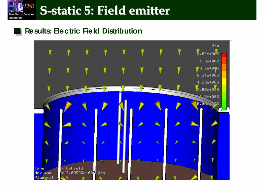
Results: Electric Field Distribution
SS--static 5: Field emitter static 5: Field emitter

Results: 1D Plot
SS--static 5: Field emitter static 5: Field emitter

Geometry
Cathode (0V) Inter-dielectric Ballast layer, a-Si
Insulator, SiO2
Gate (50V) Parameter Sweep
CNT-Floating Potential (0C)
Monitoring Point
SS--static 6: Taperedstatic 6: Tapered--type Gatedtype Gated--FEA FEA
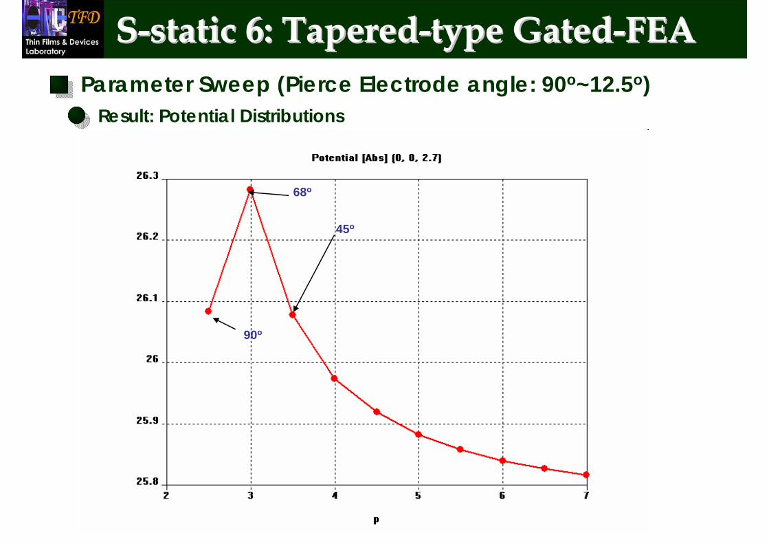
45o
68o
90o
Parameter Sweep (Pierce Electrode angle: 90o~12.5o)Result: Potential Distributions
SS--static 6: Taperedstatic 6: Tapered--type Gatedtype Gated--FEA FEA

Parameter Sweep (Pierce Electrode angle: 90o~12.5o)
45o
68o
90o
Result: Electric Field Distributions
SS--static 6: Taperedstatic 6: Tapered--type Gatedtype Gated--FEA FEA

ICP Reactor
SS--static 7: ICPstatic 7: ICP--Reactor Reactor

Simulation of ICP Reactor under DC Bias Conditions
System summary
OS: MS Windows XP V.5.1 SP1Model: Intel Zeon (SE7505VB2) 2
CPUProcess: Genuine Intel ~2790MhzMemory: 1,024.00MBGraphic Adapter: Quadro4 980XGL
Simulation summary
Tool: CST EM Studio TM v 1.3 (CST GmbH)
Simulation field: Electrostatic SolverNumber of nodes: 1,074,480Mesh generation time: 130 sSolver time: 13 s
Modeling of ICP Reactor
SS--static 7: ICPstatic 7: ICP--Reactor Reactor
Simulation

Conditions Simulation Results Under 300 V Conditions
Potential distribution
SS--static 7: ICPstatic 7: ICP--Reactor Reactor
Electric Field distribution

Conditions Simulation Results Under -450 V Conditions
Potential distribution
SS--static 7: ICPstatic 7: ICP--Reactor Reactor
Electric Field distribution

CSTCST EM StudioEM StudioExample: MExample: M--staticstatic

MM--static 1: Rotary Encoderstatic 1: Rotary EncoderIntroduction
CST EM Studio
In this tutorial a rotary encoder consisting of two iron yokes, a permanent magnet and two hall sensors is analyzed.
Both yokes form a magnetic circuit, which is driven by a cylindrical permanent magnet. Two hall sensors are placed in the air gap between the yokes to measure the flux density in the gap. By twisting the yokes the B-field changes linear with the rotation angle.
Upper Yoke(Iron 1000)
Bottom Yoke(Iron 1000)
Magnet
Hall Sensor
0.2 T|z

MM--static 1: Rotary Encoderstatic 1: Rotary Encoder
B-Field
CST EM Studio

MM--static 1: Rotary Encoderstatic 1: Rotary Encoder
Parameter Sweep
CST EM Studio
Field Watch Position

CSTCST EM StudioEM StudioExample: LF (Low Example: LF (Low Frequency) SolverFrequency) Solver

LF: Eddy Current SensorLF: Eddy Current SensorIntroduction
CST EM Studio
In this example and eddy current sensor is modeled to simulate non-destructive material test. You will analyze an eddy current sensor driven by a low frequency coil generating eddy currents in an aluminum probe plate.
The structure depicted above consists of the sensor, represented by an excitation current coil embedded in iron material. Below this sensor the probe plate is given as a lossy aluminum material, allowing the flow of eddy current. Inside this plate a material defect is modeled as a gap, which should be detected by the changing voltage at the coil.

LF: Eddy Current SensorLF: Eddy Current Sensor
CST EM Studio
B-Field (0o) Eddy Current (90o)

CSTCST EM StudioEM StudioExample: Stationary Example: Stationary Currents SolverCurrents Solver

SC: Circuit BreakerSC: Circuit BreakerIntroduction
CST EM Studio
In this example, you will analyze a circuit breaker consisting of two contact springs connected by a bridge.
One matter of concern is the current flow from one contact over the bridge to the other contact. Therefore two current port are defined for the stationary current solver. After the solver run the fields are visualized and then used as a source field for a subsequent carried out magnetostatic calculation.
Cupper(J-port, -0.05V)
Cupper(J-port, 0.05V)
Contact pad(PEC)
Bridge(PEC)

SC: Circuit BreakerSC: Circuit Breaker
CST EM Studio
Current Density
Loss Power (P): 6.856485e+001 [W]R = V2/P=0.1*0.1/P = 1.458473e-4I = P/V = V/R = 685.65 [A]

SC: Circuit BreakerSC: Circuit Breaker
CST EM Studio
H-Field

CSTCST EM StudioEM StudioExample: Tracking Example: Tracking SolverSolver

Tracking 1: Electron GunTracking 1: Electron GunIntroduction
CST EM Studio
This example demonstrated how a particle tracking can be performed. Two types of field results were used here, an electrostaic field is used to accelerate electrons being emitted from a cathode and a magnetostatic field which is caused by a helmholz coil in order to focus the electron beam.
Anode(PEC, 1000V)
Cathode(PEC, 0V)
Focus coil(0.4A)

Tracking 1: Electron GunTracking 1: Electron Gun
Particle Source
CST EM Studio
Emission Site(electron)
Particle Tracking