& gold max - farnell element14 · & gold max - farnell element14 ... gold max
TRANSCRIPT
© KEMET Electronics Corporation, P.O. Box 5928, Greenville, S.C. 29606, (864) 963-630010
CERAMIC CONFORMALLY COATED/AXIAL“AXIMAX” & GOLD MAX
GENERAL SPECIFICATIONS Working Voltage: Axial (WVDC)
C0G 50, 100, 200 X7R 25, 50, 100, 200, 250
Z5U 50, 100 Radial (WVDC)
C0G 50, 100, 200, 500, 1k, 1.5k, 2k, 2.5k, 3k X7R 25, 50, 100, 200, 250, 500, 1k, 1.5k, 2k, 2.5k, 3k
Z5U 50, 100
Temperature Characteristics: C0G 0 ±30 PPM / °C from -55°C to +125°C (1) X7R ± 15% from -55°C to +125°C Z5U + 22%, -56% from +10°C to +85°C
Capacitance Tolerance:C0G ±0.5pF, ±1%, ±2%, ±5%, ±10%, ±20%
X7R ±10%, ±20%, +80% / -20% Z5U ±20%, 80% / -20%
Construction:Epoxy encapsulated – meets flame test requirements
of UL Standard 94V-0. High-temperature solder – meets EIA RS-198, Method 302, Condition B (260°C for 10 seconds)
Lead Material: Standard: 100% matte tin (Sn) with nickel (Ni) underplate and steel core ( “TA” designation).
Alternative 1: 60% Tin (Sn)/40% Lead (Pb) finish with copper- clad steel core ( “HA” designation).
Alternative 2: 60% Tin (Sn)/40% Lead (Pb) finish with 100%copper core (available with “HA” termination code with c-spec)
Solderability:
EIA RS-198, Method 301, Solder Temperature: 230°C ±5°C. Dwell time in solder = 7 ± seconds.
Terminal Strength: EIA RS-198, Method 303, Condition A (2.2kg) ELECTRICAL
Capacitance @ 25°C: Within specified tolerance and following test conditions. C0G – >1000pF with 1.0 vrms @ 1 kHz 1000pF with 1.0 vrms @ 1 MHz X7R – with 1.0 vrms @ 1 kHz (Referee Time: 1,000 hours)
Z5U – with 1.0 vrms @ 1 kHz
Dissipation Factor @25°C: Same test conditions as capacitance. C0G – 0.10% maximum X7R – 2.5% maximum (3.5% for 25V)
Z5U – 4.0% maximum
Insulation Resistance @25°C: EIA RS-198, Method 104, Condition A <1kV
C0G – 100 G or 1000 M – F, whichever is less. 500V test @ rated voltage, >500V test @ 500V X7R – 100 G or 1000 M – F, whichever is less. 500V test @ rated voltage, >500V test @ 500V
Z5U – 10 G or 1000 M – F, whichever is less.
Dielectric Withstanding Voltage: EIA RS-198, Method 103
250V test @ 250% of rated voltage for 5 secondswith current limited to 50mA.
500V test @ 150% of rated voltage for 5 secondswith current limited to 50mA.
1000V test @ 120% of rated voltage for 5 seconds with current limited to 50mA.
ENVIRONMENTAL Vibration:
with current limited to 50mA.
ENVIRONMENTAL Vibration:
EIA RS-198, Method 304, Condition D (10-2000Hz; 20g) Shock: EIA RS-198, Method 305, Condition I (100g)
Life Test:EIA RS-198, Method 201, Condition D.
<200VC0G – 200% of rated voltage @ +125°C
X7R – 200% of rated voltage @ +125°C Z5U – 200% of rated voltage @ +85°C >500V C0G – rated voltage @ +125°C X7R – rated voltage @ +125°C
Post Test Limits @ 25°C are: Capacitance Change: C0G ( 200V) – ±3% or 0.25pF, whichever is greater.
C0G ( 500V) – ±3% or 0.50pF, whichever is greater.X7R – ± 20% of initial value (2)
Z5U – ± 30% of initial value (2) Dissipation Factor: C0G – 0.10% maximum X7R – 2.5% maximum (3.5% for 25V)
Z5U – 4.0% maximum Insulation Resistance: C0G – 10 G or 100 M – F, whichever is less. >1kV tested @ 500V.
X7R – 10 G or 100 M – F, whichever is less. >1kV tested @ 500V.
Z5U – 1 G or 100 M – F, whichever is less.
Moisture Resistance:EIA RS-198, Method 204, Condition A (10 cycles
without applied voltage). Post Test Limits @ 25°C are: Capacitance Change: C0G ( 200V) – ±3% or ±0.25pF, whichever is greater.
C0G ( 500V) – ±3% or ± 0.50pF, whichever is greater.X7R – ± 20% of initial value (2)
Z5U – ± 30% of initial value (2) Dissipation Factor: C0G – 0.10% maximum X7R – 2.5% maximum (3.5% for 25V)
Z5U – 4.0% maximum Insulation Resistance: C0G – 10 G or 100 M – Fwhichever is less.
500V test @ rated voltage, >500V test @ 500V.X7R – 10 G or 100 M – F, whichever is less.
500V test @ rated voltage, >500V test @ 500V.Z5U – 1k M or 100 M – F, whichever is less.
Thermal Shock:
EIA RS-198, Method 202, Condition B (C0G & X7R: -55°C to 125°C); Condition A (Z5U: -55°C to 85°C)
(1) +53 PPM -30 PPM/ °C from +25°C to -55°C, + 60 PPM below 10pF. (2) X7R and Z5U dielectrics exhibit aging characteristics; therefore, it is highly recommended that capacitors be deaged for 2 hours at 150°C and stabilized at room temperature for 48 hours before capacitance measurements are made.
© KEMET Electronics Corporation, P.O. Box 5928, Greenville, S.C. 29606, (864) 963-6300 15
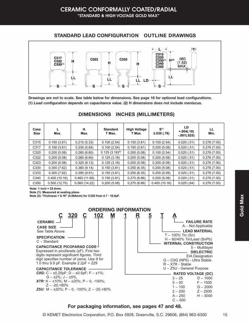
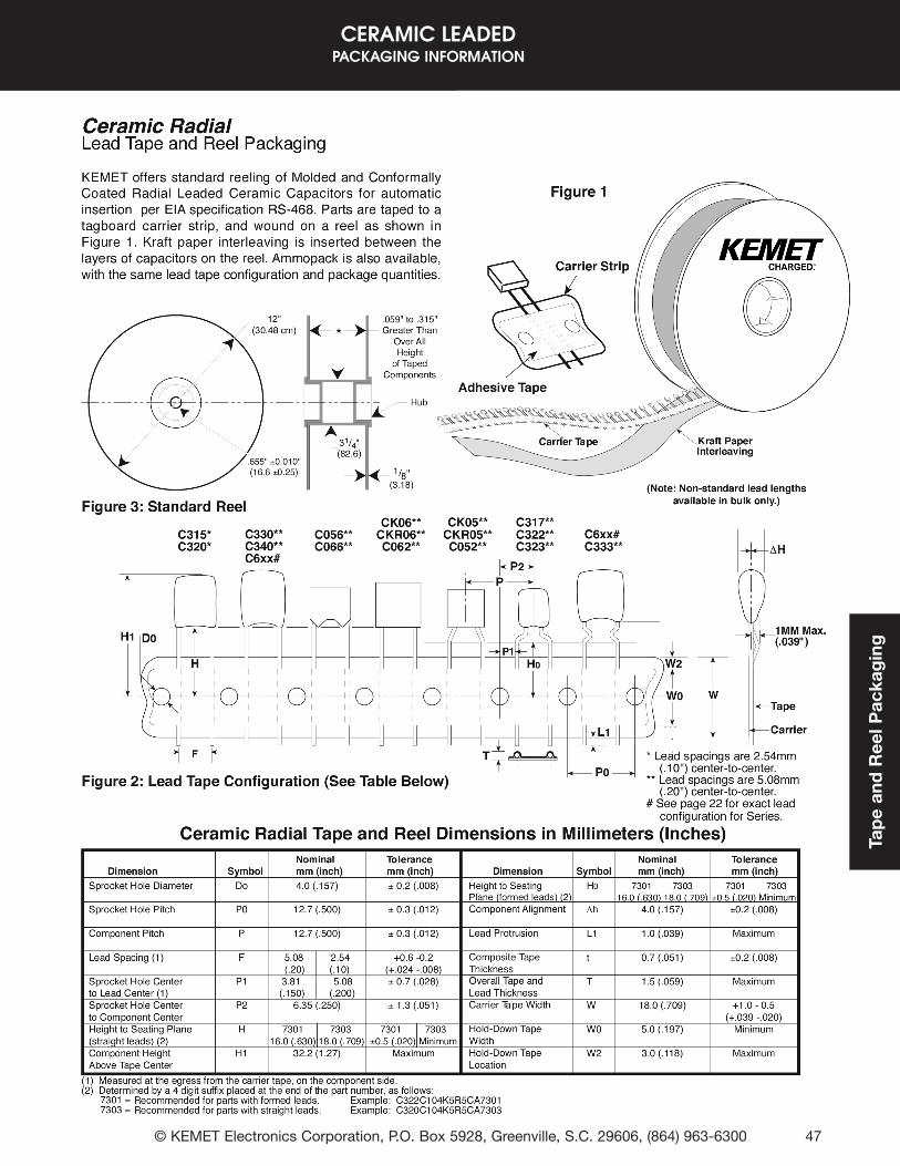
DIMENSIONS Ñ INCHES (MILLIMETERS)
For packaging information, see pages 47 and 48.
ORDERING INFORMATION
Drawings are not to scale. See table below for dimensions. See page 16 for optional lead configurations. (1) Lead configuration depends on capacitance value. (2) H dimensions does not include meniscus.
STANDARD LEAD CONFIGURATION Ñ OUTLINE DRAWINGS
CERAMIC CONFORMALLY COATED/RADIAL“STANDARD & HIGH VOLTAGE GOLD MAX”
Go
ldM
ax
CaseSize
LMax.
H.Max.
StandardT Max.
High VoltageT Max.
S(1)
±.030 (.78)
LD+.004(.10)-.001(.025)
LLMin.
C315 0.150 (3.81) 0.210 (5.33) 0.100 (2.54) 0.150 (3.81) 0.100 (2.54) 0.020 (.51) 0.276 (7.00)C317 0.150 (3.81) 0.230 (5.84) 0.100 (2.54) 0.150 (3.81) 0.200 (5.08) 0.020 (.51) 0.276 (7.00)C320 0.200 (5.08) 0.260 (6.60) 0.125 (3.18)(2) 0.200 (5.08) 0.100 (2.54) 0.020 (.51) 0.276 (7.00)C322 0.200 (5.08) 0.260 (6.60) 0.125 (3.18) 0.200 (5.08) 0.200 (5.08) 0.020 (.51) 0.276 (7.00)C323 0.200 (5.08) 0.320 (8.13) 0.125 (3.18) 0.200 (5.08) 0.200 (5.08) 0.020 (.51) 0.276 (7.00)C330 0.300 (7.62) 0.360 (9.14) 0.150 (3.81) 0.250 (6.35) 0.200 (5.08) 0.020 (.51) 0.276 (7.00)C333 0.300 (7.62) 0.390 (9.91) 0.150 (3.81) 0.250 (6.35) 0.200 (5.08) 0.020 (.51) 0.276 (7.00)C340 0.400 (10.16) 0.460 (11.68) 0.150 (3.81) 0.270 (6.86) 0.200 (5.08) 0.020 (.51) 0.276 (7.00)C350 0.500 (12.70) 0.560 (14.22) 0.200 (5.08) 0.270 (6.86) 0.400 (10.16) 0.025 (.64) 0.276 (7.00)
Note: 1 inch = 25.4mm.Note (1): Measured at seating plane.Note (2): Thickness = 0.16" (4.064mm) for C320 from 4.7 - 10.0 F.
(1)
(1)
C 320 C 102 M 1 R 5 T ACERAMICCASE SIZESee Table Above
SPECIFICATIONC – StandardCAPACITANCE PICOFARAD CODEExpressed in picofarads (pF). First twodigits represent significant figures. Thirddigit specifies number of zeros. Use 9 for1.0 thru 9.9 pF. Example 2.2pF = 229CAPACITANCE TOLERANCEC0G: C – ±0.25pF; D – ±0.5pF; F – ±1%;
G – ±2%; J – ±5%,X7R: K – ±10%; M – ±20%; P – 0, -100%;
Z – -20,+80%Z5U: M – ±20%; P – 0, -100%; Z – -20,+80%
RATED VOLTAGE (DC)3 – 25 D – 10005 – 50 F – 15001 – 100 G – 20002 – 200 Z – 2500A – 250 H – 3000C – 500
FAILURE RATEA – Not ApplicableLEAD MATERIAL
T – 100% Tin (Sn)H – 60/40% Tin/Lead (SnPb)
INTERNAL CONSTRUCTION5 – MultilayerDIELECTRIC
EIA DesignationG – C0G (NP0) - Ultra StableR – X7R - StableU – Z5U - General Purpose
© KEMET Electronics Corporation, P.O. Box 5928, Greenville, S.C. 29606, (864) 963-630016
CERAMIC CONFORMALLY COATED/RADIAL“STANDARD & HIGH VOLTAGE GOLD MAX”
Lead Spacing.100" ± .030
Lead Spacing.200" ± .030
Lead Spacing.200" ± .030
Lead Spacing.200" ± .030
Lead Spacing Lead Spacing
.150MAX.
.210MAX.
.276MIN.
.100
C 3 1 5
.150MAX.
.230MAX.
.230±.030
.100
C 3 1 6
.200
.200MAX.
.260MAX.
.276MIN.
.200
C 3 2 2 C 3 2 3
.320MAX.
.276MIN.
.200
.200MAX.
.150MAX.
.230MAX.
.276MIN.
.200
C 3 1 7
.150MAX.
.235MAX.
.276MIN.
.200
C 3 1 8
.200MAX.
.325MAX.
.276MIN.
C 3 2 8
.200
.200MAX.
.350MAX.
.230±.030
.200
C 3 2 7
.270
.200MAX.
.320MAX.
.276MIN.
.200
C 3 2 5
.300MAX.
.360MAX.
.276MIN.
.250
C 3 3 1
.200MAX.
.260MAX.
.276MIN.
.250
C 3 2 1
.500MAX.
.560MAX.
.276MIN.
.400
C 3 5 0
.500MAX.
.670MAX.
.230±.030
C 3 5 6
.400
.520
.400MAX.
.590MAX.
.230±.030
.200
C 3 4 6
.320
.400MAX.
.460MAX.
.276MIN.
.200
C 3 4 0
.200MAX.
.260MAX.
.276MIN.
.100
C 3 2 0
.200MAX.
.260MAX.
.276MIN.
.100
C 3 2 4 C 3 2 6
.230± .030
.100
.200MAX.
.350MAX.
.300MAX.
.360MAX.
.276MIN.
.200
C 3 3 0
.300MAX.
.390MAX.
.276MIN.
.200
C 3 3 3
.300MAX.
.420MAX.
.276MIN.
.200
C 3 3 5
.300MAX.
.450MAX.
.230±.030
.200
C 3 3 6
.300
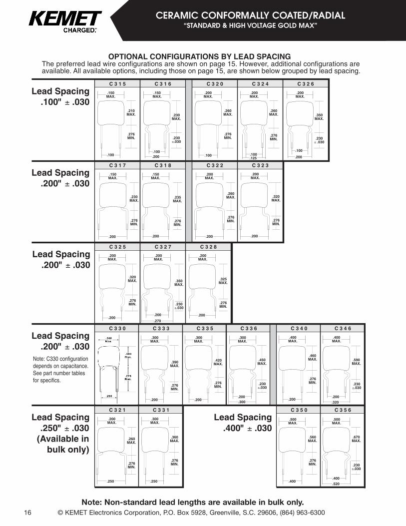
The preferred lead wire configurations are shown on page 15. However, additional configurations areavailable. All available options, including those on page 15, are shown below grouped by lead spacing.
OPTIONAL CONFIGURATIONS BY LEAD SPACING
.200.125
.250" ± .030(Available in
bulk only)
.400" ± .030
Note: Non-standard lead lengths are available in bulk only.
Note: C330 configurationdepends on capacitance.See part number tables for specifics.
© KEMET Electronics Corporation, P.O. Box 5928, Greenville, S.C. 29606, (864) 963-6300 17
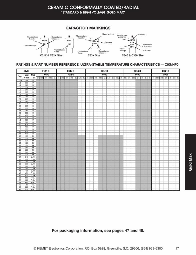
CAPACITOR MARKINGS
Manufacturer(KEMET)
Rated Voltage5 - 50 volts1 - 100 volts2 - 200 volts
CapacitanceTolerance
Manufacturer(KEMET)
Capacitance& Tolerance
DielectricC0GX7RZ5U
RatedVoltageCapacitance
CodeDate Code
Front
K1K
Back
102
C31X & C32X Size
KX7R105K100V0814
C340 & C350 Size
Rated Voltage5 - 50 volts1 - 100 volts2 - 200 volts
Manufacturer(KEMET)
CapacitanceTolerance
CapacitanceCode
DielectricG - C0GR - X7RU - Z5U
K5U104M
C33X Size
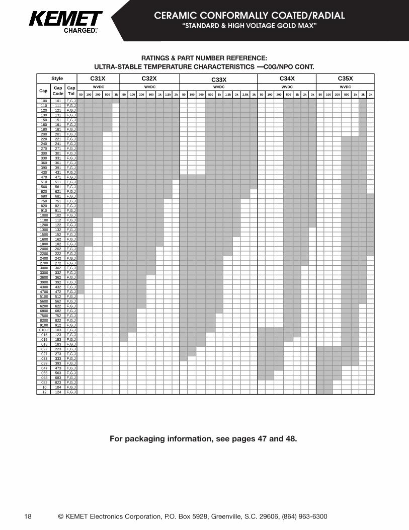
RATINGS & PART NUMBER REFERENCE: ULTRA-STABLE TEMPERATURE CHARACTERISTICS — C0G/NP0
For packaging information, see pages 47 and 48.
Go
ldM
ax
CERAMIC CONFORMALLY COATED/RADIAL“STANDARD & HIGH VOLTAGE GOLD MAX”
50 100 200 500 1k 50 100 200 500 1k 1.5k 2k 50 100 200 500 1k 1.5k 2k 2.5k 3k 50 100 200 500 1k 2k 3k 50 100 200 500 1k 2k 3k
1.0pF 109 D1.1 119 D1.2 129 D1.3 139 D1.5 159 D1.6 169 D1.8 189 D2.0 209 D2.2 229 D2.4 249 D2.7 279 D3.0 309 D3.3 339 D3.6 369 D3.9 399 D4.3 439 D4.7 479 D5.1 519 D5.6 569 D6.2 629 D6.8 689 D7.5 759 D8.2 829 D9.1 919 D10 100 J,K11 110 J,K12 120 J,K13 130 J,K15 150 J,K16 160 J,K18 180 J,K20 200 J,K22 220 J,K24 240 G,J,K27 270 G,J,K30 300 G,J,K33 330 G,J,K36 360 G,J,K39 390 G,J,K43 430 G,J,K47 470 G,J,K51 510 G,J,K56 560 F,G,J62 620 F,G,J68 680 F,G,J75 750 F,G,J82 820 F,G,J91 910 F,G,J
WVDCWVDC WVDC WVDC WVDC
C35XC31X C32X C33X C34XStyle
Cap CapCode
CapTol
© KEMET Electronics Corporation, P.O. Box 5928, Greenville, S.C. 29606, (864) 963-630018
CERAMIC CONFORMALLY COATED/RADIAL“STANDARD & HIGH VOLTAGE GOLD MAX”
For packaging information, see pages 47 and 48.
RATINGS & PART NUMBER REFERENCE: ULTRA-STABLE TEMPERATURE CHARACTERISTICS —C0G/NPO CONT.
50 100 200 500 1k 50 100 200 500 1k 1.5k 2k 50 100 200 500 1k 1.5k 2k 2.5k 3k 50 100 200 500 1k 2k 3k 50 100 200 500 1k 2k 3k
100 101 F,G,J110 111 F,G,J120 121 F,G,J130 131 F,G,J150 151 F,G,J160 161 F,G,J180 181 F,G,J200 201 F,G,J220 221 F,G,J240 241 F,G,J270 271 F,G,J300 301 F,G,J330 331 F,G,J360 361 F,G,J390 391 F,G,J430 431 F,G,J470 471 F,G,J510 511 F,G,J560 561 F,G,J620 621 F,G,J680 681 F,G,J750 751 F,G,J820 821 F,G,J910 911 F,G,J1000 102 F,G,J1100 112 F,G,J1200 122 F,G,J1300 132 F,G,J1500 152 F,G,J1600 162 F,G,J1800 182 F,G,J2000 202 F,G,J2200 222 F,G,J2400 242 F,G,J2700 272 F,G,J3000 302 F,G,J3300 332 F,G,J3600 362 F,G,J3900 392 F,G,J4300 432 F,G,J4700 472 F,G,J5100 512 F,G,J5600 562 F,G,J6200 622 F,G,J6800 682 F,G,J7500 752 F,G,J8200 822 F,G,J9100 912 F,G,J
.010uF 103 F,G,J.015 123 F,G,J.015 153 F,G,J.018 183 F,G,J.022 223 F,G,J.027 273 F,G,J.033 333 F,G,J.039 393 F,G,J.047 473 F,G,J.056 563 F,G,J.068 683 F,G,J.082 823 F,G,J.10 104 F,G,J.12 124 F,G,J
C34X C35XWVDC WVDC WVDC WVDC WVDC
C32X C31X
Cap CapCode
CapTol
C33XStyle
© KEMET Electronics Corporation, P.O. Box 5928, Greenville, S.C. 29606, (864) 963-6300 19
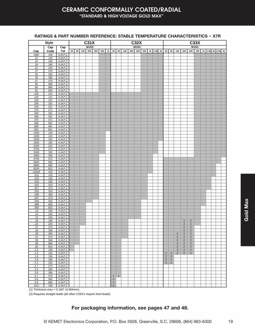
RATINGS & PART NUMBER REFERENCE: STABLE TEMPERATURE CHARACTERISTICS - X7R
Go
ldM
ax
CERAMIC CONFORMALLY COATED/RADIAL“STANDARD & HIGH VOLTAGE GOLD MAX”
Cap CapCap Code Tol 25 50 100 200 250 500 1k 25 50 100 200 250 500 1k 1.5k 2k 25 50 100 200 250 500 1k 1.5k 2k 2.5k 3k
10pF 100 K,M,P,Z12 120 K,M,P,Z15 150 K,M,P,Z18 180 K,M,P,Z22 220 K,M,P,Z27 270 K,M,P,Z33 330 K,M,P,Z39 390 K,M,P,Z47 470 K,M,P,Z56 560 K,M,P,Z68 680 K,M,P,Z82 820 K,M,P,Z
100 101 K,M,P,Z120 121 K,M,P,Z150 151 K,M,P,Z180 181 K,M,P,Z220 221 K,M,P,Z270 271 K,M,P,Z330 331 K,M,P,Z390 391 K,M,P,Z470 471 K,M,P,Z560 561 K,M,P,Z680 681 K,M,P,Z820 821 K,M,P,Z
1000 102 K,M,P,Z1200 122 K,M,P,Z1500 152 K,M,P,Z1800 182 K,M,P,Z2200 222 K,M,P,Z2700 272 K,M,P,Z3300 332 K,M,P,Z3900 392 K,M,P,Z4700 472 K,M,P,Z5600 562 K,M,P,Z6800 682 K,M,P,Z8200 822 K,M,P,Z
.010uF 103 K,M,P,Z.012 123 K,M,P,Z.015 153 K,M,P,Z.018 183 K,M,P,Z.022 223 K,M,P,Z.027 273 K,M,P,Z.033 333 K,M,P,Z.039 393 K,M,P,Z.047 473 K,M,P,Z.056 563 K,M,P,Z.068 683 K,M,P,Z.082 823 K,M,P,Z.10 104 K,M,P,Z.12 124 K,M,P,Z.15 154 K,M,P,Z.18 184 K,M,P,Z 2 2.22 224 K,M,P,Z 2 2.27 274 K,M,P,Z 2 2.33 334 K,M,P,Z 2 2.39 394 K,M,P,Z 2 2 2.47 474 K,M,P,Z 2 2 2.56 564 K,M,P,Z 2 2 2.68 684 K,M,P,Z 2 2 2.82 824 K,M,P,Z 2 2 21.0 105 K,M,P,Z 2 2 21.2 125 K,M,P,Z 2 2 2 2 21.5 155 K,M,P,Z 2 21.8 185 K,M,P,Z 2 22.2 225 K,M,P,Z 2 22.7 275 K,M,P,Z3.3 335 K,M,P,Z3.9 395 K,M,P,Z4.7 475 K,M,P,Z 1 15.6 565 K,M,P,Z 16.8 685 K,M,P,Z 1
10.0 106 K,M,P,Z 1(1) Thickness max = 0.160" (4.064mm)(2) Requires straight leads (all other C33X's require bent leads)
C32X Style C31X WVDC WVDCWVDC
C33X
For packaging information, see pages 47 and 48.
© KEMET Electronics Corporation, P.O. Box 5928, Greenville, S.C. 29606, (864) 963-630020
CERAMIC CONFORMALLY COATED/RADIAL“STANDARD & HIGH VOLTAGE GOLD MAX”
For packaging information, see pages 47 and 48.
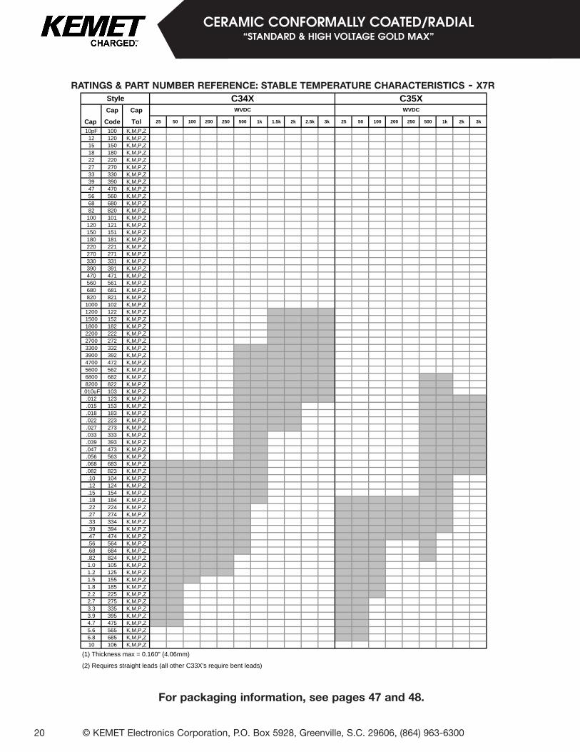
RATINGS & PART NUMBER REFERENCE: STABLE TEMPERATURE CHARACTERISTICS - X7R
Cap Cap
Cap Code Tol 25 50 100 200 250 500 1k 1.5k 2k 2.5k 3k 25 50 100 200 250 500 1k 2k 3k
10pF 100 K,M,P,Z12 120 K,M,P,Z15 150 K,M,P,Z18 180 K,M,P,Z22 220 K,M,P,Z27 270 K,M,P,Z33 330 K,M,P,Z39 390 K,M,P,Z47 470 K,M,P,Z56 560 K,M,P,Z68 680 K,M,P,Z82 820 K,M,P,Z100 101 K,M,P,Z120 121 K,M,P,Z150 151 K,M,P,Z180 181 K,M,P,Z220 221 K,M,P,Z270 271 K,M,P,Z330 331 K,M,P,Z390 391 K,M,P,Z470 471 K,M,P,Z560 561 K,M,P,Z680 681 K,M,P,Z820 821 K,M,P,Z1000 102 K,M,P,Z1200 122 K,M,P,Z1500 152 K,M,P,Z1800 182 K,M,P,Z2200 222 K,M,P,Z2700 272 K,M,P,Z3300 332 K,M,P,Z3900 392 K,M,P,Z4700 472 K,M,P,Z5600 562 K,M,P,Z6800 682 K,M,P,Z8200 822 K,M,P,Z
.010uF 103 K,M,P,Z.012 123 K,M,P,Z.015 153 K,M,P,Z.018 183 K,M,P,Z.022 223 K,M,P,Z.027 273 K,M,P,Z.033 333 K,M,P,Z.039 393 K,M,P,Z.047 473 K,M,P,Z.056 563 K,M,P,Z.068 683 K,M,P,Z.082 823 K,M,P,Z.10 104 K,M,P,Z.12 124 K,M,P,Z.15 154 K,M,P,Z.18 184 K,M,P,Z.22 224 K,M,P,Z.27 274 K,M,P,Z.33 334 K,M,P,Z.39 394 K,M,P,Z.47 474 K,M,P,Z.56 564 K,M,P,Z.68 684 K,M,P,Z.82 824 K,M,P,Z1.0 105 K,M,P,Z1.2 125 K,M,P,Z1.5 155 K,M,P,Z1.8 185 K,M,P,Z2.2 225 K,M,P,Z2.7 275 K,M,P,Z3.3 335 K,M,P,Z3.9 395 K,M,P,Z4.7 475 K,M,P,Z5.6 565 K,M,P,Z6.8 685 K,M,P,Z10 106 K,M,P,Z
(1) Thickness max = 0.160" (4.06mm)
(2) Requires straight leads (all other C33X's require bent leads)
StyleWVDC
C34X C35XWVDC
© KEMET Electronics Corporation, P.O. Box 5928, Greenville, S.C. 29606, (864) 963-6300 21
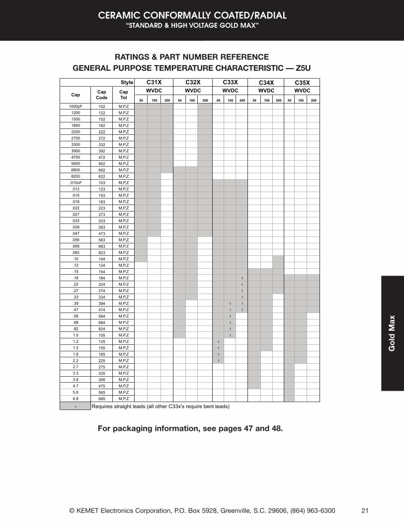
50 100 200 50 100 200 50 100 200 50 100 200 50 100 200
1000pF 102 M,P,Z1200 122 M,P,Z1500 152 M,P,Z1800 182 M,P,Z2200 222 M,P,Z2700 272 M,P,Z3300 332 M,P,Z3900 392 M,P,Z4700 472 M,P,Z5600 562 M,P,Z6800 682 M,P,Z8200 822 M,P,Z
.010uF 103 M,P,Z.012 123 M,P,Z.015 153 M,P,Z.018 183 M,P,Z.022 223 M,P,Z.027 273 M,P,Z.033 333 M,P,Z.039 393 M,P,Z.047 473 M,P,Z.056 563 M,P,Z.068 683 M,P,Z.082 823 M,P,Z.10 104 M,P,Z.12 124 M,P,Z.15 154 M,P,Z.18 184 M,P,Z 1
.22 224 M,P,Z 1
.27 274 M,P,Z 1
.33 334 M,P,Z 1
.39 394 M,P,Z 1 1
.47 474 M,P,Z 1 1
.56 564 M,P,Z 1
.68 684 M,P,Z 1
.82 824 M,P,Z 1
1.0 105 M,P,Z 1
1.2 125 M,P,Z 1
1.5 155 M,P,Z 1
1.8 185 M,P,Z 1
2.2 225 M,P,Z 1
2.7 275 M,P,Z3.3 335 M,P,Z3.9 395 M,P,Z4.7 475 M,P,Z5.6 565 M,P,Z6.8 685 M,P,Z
1 Requires straight leads (all other C33x's require bent leads)
C35XC31X C32X C34XC33XStyle
Cap CapCode
CapTol
WVDCWVDC WVDC WVDC WVDC
RATINGS & PART NUMBER REFERENCEGENERAL PURPOSE TEMPERATURE CHARACTERISTIC — Z5U
For packaging information, see pages 47 and 48.
Go
ldM
ax
CERAMIC CONFORMALLY COATED/RADIAL“STANDARD & HIGH VOLTAGE GOLD MAX”
© KEMET Electronics Corporation, P.O. Box 5928, Greenville, S.C. 29606, (864) 963-6300 47
Tap
ean
dR
eelP
acka
gin
g
CERAMIC LEADEDPACKAGING INFORMATION
© KEMET Electronics Corporation, P.O. Box 5928, Greenville, S.C. 29606, (864) 963-630048
CERAMIC LEADEDPACKAGING INFORMATION
KEMETSeries
MilitaryStyle
MilitarySpecification
Standard (1)Bulk
Quantity
Ammo PackQuantity
Maximum
MaximumReel
Quantity
ReelSize
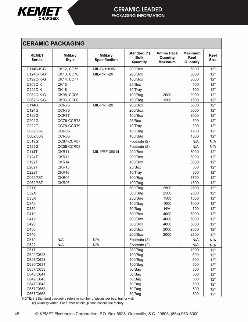
C114C-K-G CK12, CC75 MIL-C-11015/ 200/Box 5000 12"C124C-K-G CK13, CC76 MIL-PRF-20 200/Box 5000 12"C192C-K-G CK14, CC77 100/Box 3000 12"C202C-K CK15 25/Box 500 12"C222C-K CK16 10/Tray 300 12"C052C-K-G CK05, CC05 100/Bag 2000 2000 12"C062C-K-G CK06, CC06 100/Bag 1500 1500 12"C114G CCR75 MIL-PRF-20 200/Box 5000 12"C124G CCR76 200/Box 5000 12"C192G CCR77 100/Box 3000 12"C202G CC78-CCR78 25/Box 500 12"C222G CC79-CCR79 10/Tray 300 12"C052/56G CCR05 100/Bag 1700 12"C062/66G CCR06 100/Bag 1500 12"C512G CC07-CCR07 Footnote (2) N/A N/AC522G CC08-CCR08 Footnote (2) N/A N/AC114T CKR11 MIL-PRF-39014 200/Box 5000 12"C124T CKR12 200/Box 5000 12"C192T CKR14 100/Box 3000 12"C202T CKR15 25/Box 500 12"C222T CKR16 10/Tray 300 12"C052/56T CKR05 100/Bag 1700 12"C062/66T CKR06 100/Bag 1500 12"C31X 500/Bag 2500 2500 12"C32X 500/Bag 2500 2500 12"C33X 250/Bag 1500 1500 12"C340 100/Bag 1000 1000 12"C350 50/Bag N/A 500 12"C410 300/Box 4000 5000 12"C412 200/Box 4000 5000 12"C420 300/Box 4000 5000 12"C430 200/Box 2000 2500 12"C440 200/Box 2000 2500 12"C512 N/A N/A Footnote (2) N/A N/AC522 N/A N/A Footnote (2) N/A N/AC617 250/Bag 1000 12"C622/C623 100/Bag 500 12"C627/C628 100/Bag 500 12"C630/C631 100/Bag 500 12"C637/C638 50/Bag 500 12"C640/C641 50/Bag 500 12"C642/C643 50/Bag 500 12"C647/C648 50/Bag 500 12"C657/C658 50/Bag 500 12"C667/C668 50/Bag 500 12"
CERAMIC PACKAGING
NOTE: (1) Standard packaging refers to number of pieces per bag, tray or vial.(2) Quantity varies. For further details, please consult the factory.
© KEMET Electronics Corporation, P.O. Box 5928, Greenville, S.C. 29606, (864) 963-63004
MULTILAYER CERAMIC CAPACITORS/AXIAL & RADIAL LEADED
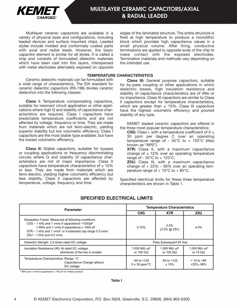
Multilayer ceramic capacitors are available in avariety of physical sizes and configurations, includingleaded devices and surface mounted chips. Leadedstyles include molded and conformally coated partswith axial and radial leads. However, the basiccapacitor element is similar for all styles. It is called achip and consists of formulated dielectric materialswhich have been cast into thin layers, interspersedwith metal electrodes alternately exposed on opposite
edges of the laminated structure. The entire structure isfired at high temperature to produce a monolithicblock which provides high capacitance values in asmall physical volume. After firing, conductiveterminations are applied to opposite ends of the chip tomake contact with the exposed electrodes.Termination materials and methods vary depending onthe intended use.
TEMPERATURE CHARACTERISTICSCeramic dielectric materials can be formulated with
a wide range of characteristics. The EIA standard forceramic dielectric capacitors (RS-198) divides ceramicdielectrics into the following classes:
Class I: Temperature compensating capacitors,suitable for resonant circuit application or other appli-cations where high Q and stability of capacitance char-acteristics are required. Class I capacitors havepredictable temperature coefficients and are notaffected by voltage, frequency or time. They are madefrom materials which are not ferro-electric, yieldingsuperior stability but low volumetric efficiency. Class Icapacitors are the most stable type available, but havethe lowest volumetric efficiency.
Class II: Stable capacitors, suitable for bypassor coupling applications or frequency discriminatingcircuits where Q and stability of capacitance char-acteristics are not of major importance. Class IIcapacitors have temperature characteristics of ± 15%or less. They are made from materials which areferro-electric, yielding higher volumetric efficiency butless stability. Class II capacitors are affected bytemperature, voltage, frequency and time.
Class III: General purpose capacitors, suitablefor by-pass coupling or other applications in whichdielectric losses, high insulation resistance andstability of capacitance characteristics are of little orno importance. Class III capacitors are similar to ClassII capacitors except for temperature characteristics,which are greater than ± 15%. Class III capacitorshave the highest volumetric efficiency and pooreststability of any type.
KEMET leaded ceramic capacitors are offered inthe three most popular temperature characteristics:
C0G: Class I, with a temperature coefficient of 0 ±30 ppm per degree C over an operatingtemperature range of - 55°C to + 125°C (Alsoknown as “NP0”).X7R: Class II, with a maximum capacitancechange of ± 15% over an operating temperaturerange of - 55°C to + 125°C.Z5U: Class III, with a maximum capacitancechange of + 22% - 56% over an operating tem-perature range of + 10°C to + 85°C.
Specified electrical limits for these three temperaturecharacteristics are shown in Table 1.
SPECIFIED ELECTRICAL LIMITS
Table I
C0G X7R Z5U
Dissipation Factor: Measured at following conditions.C0G – 1 kHz and 1 vrms if capacitance >1000pF
1 MHz and 1 vrms if capacitance 1000 pFX7R – 1 kHz and 1 vrms* or if extended cap range 0.5 vrmsZ5U – 1 kHz and 0.5 vrms
0.10% 2.5%(3.5% @ 25V) 4.0%
Dielectric Stength: 2.5 times rated DC voltage.
Insulation Resistance (IR): At rated DC voltage,whichever of the two is smaller
1,000 M For 100 G
1,000 M For 100 G
1,000 M For 10 G
Temperature Characteristics: Range, °CCapacitance Change withoutDC voltage
-55 to +1250 ± 30 ppm/°C
-55 to +125± 15%
+ 10 to +85+22%,-56%
* MHz and 1 vrms if capacitance 100 pF on military product.
Parameter Temperature Characteristics
Pass Subsequent IR Test
ELECTRICAL CHARACTERISTICS
The fundamental electrical properties of multilayerceramic capacitors are as follows:
Polarity: Multilayer ceramic capacitors are not polar,and may be used with DC voltage applied in either direction.
Rated Voltage: This term refers to the maximum con-tinuous DC working voltage permissible across the entireoperating temperature range. Multilayer ceramic capacitorsare not extremely sensitive to voltage, and brief applicationsof voltage above rated will not result in immediate failure.However, reliability will be reduced by exposure to sustainedvoltages above rated.
Capacitance: The standard unit of capacitance is thefarad. For practical capacitors, it is usually expressed inmicrofarads (10-6 farad), nanofarads (10-9 farad), or picofarads(10-12 farad). Standard measurement conditions are asfollows:
Class I (up to 1,000 pF): 1MHz and 1.2 VRMSmaximum.
Class I (over 1,000 pF): 1kHz and 1.2 VRMSmaximum.
Class II: 1 kHz and 1.0 ± 0.2 VRMS.
Class III: 1 kHz and 0.5 ± 0.1 VRMS.
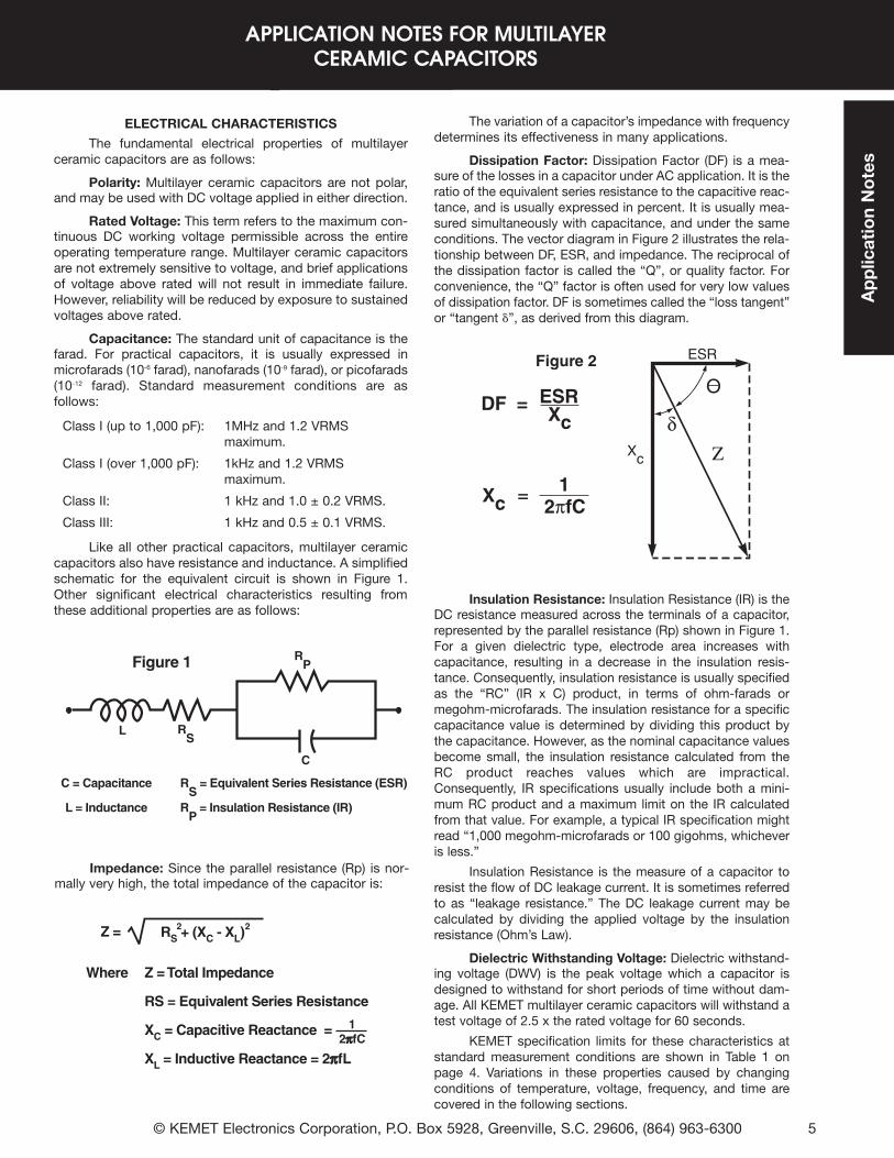
Like all other practical capacitors, multilayer ceramiccapacitors also have resistance and inductance. A simplifiedschematic for the equivalent circuit is shown in Figure 1.Other significant electrical characteristics resulting fromthese additional properties are as follows:
Impedance: Since the parallel resistance (Rp) is nor-mally very high, the total impedance of the capacitor is:
Figure 1
C = Capacitance
L = Inductance
RS
= Equivalent Series Resistance (ESR)
RP
= Insulation Resistance (IR)
RP
RS
C
L
Z =
Where Z = Total Impedance
RS = Equivalent Series Resistance
XC = Capacitive Reactance = 2ππfC
XL = Inductive Reactance = 2ππfL
1
RS + (XC - XL)2 2
DF = ESRXc
Xc 2πfC1=
Figure 2
δΖ
O
Xc
ESR
The variation of a capacitor’s impedance with frequencydetermines its effectiveness in many applications.
Dissipation Factor: Dissipation Factor (DF) is a mea-sure of the losses in a capacitor under AC application. It is theratio of the equivalent series resistance to the capacitive reac-tance, and is usually expressed in percent. It is usually mea-sured simultaneously with capacitance, and under the sameconditions. The vector diagram in Figure 2 illustrates the rela-tionship between DF, ESR, and impedance. The reciprocal ofthe dissipation factor is called the “Q”, or quality factor. Forconvenience, the “Q” factor is often used for very low valuesof dissipation factor. DF is sometimes called the “loss tangent”or “tangent d”, as derived from this diagram.
Insulation Resistance: Insulation Resistance (IR) is theDC resistance measured across the terminals of a capacitor,represented by the parallel resistance (Rp) shown in Figure 1.For a given dielectric type, electrode area increases withcapacitance, resulting in a decrease in the insulation resis-tance. Consequently, insulation resistance is usually specifiedas the “RC” (IR x C) product, in terms of ohm-farads ormegohm-microfarads. The insulation resistance for a specificcapacitance value is determined by dividing this product bythe capacitance. However, as the nominal capacitance valuesbecome small, the insulation resistance calculated from theRC product reaches values which are impractical.Consequently, IR specifications usually include both a mini-mum RC product and a maximum limit on the IR calculatedfrom that value. For example, a typical IR specification mightread “1,000 megohm-microfarads or 100 gigohms, whicheveris less.”
Insulation Resistance is the measure of a capacitor toresist the flow of DC leakage current. It is sometimes referredto as “leakage resistance.” The DC leakage current may becalculated by dividing the applied voltage by the insulationresistance (Ohm’s Law).
Dielectric Withstanding Voltage: Dielectric withstand-ing voltage (DWV) is the peak voltage which a capacitor isdesigned to withstand for short periods of time without dam-age. All KEMET multilayer ceramic capacitors will withstand atest voltage of 2.5 x the rated voltage for 60 seconds.
KEMET specification limits for these characteristics atstandard measurement conditions are shown in Table 1 onpage 4. Variations in these properties caused by changingconditions of temperature, voltage, frequency, and time arecovered in the following sections.
© KEMET Electronics Corporation, P.O. Box 5928, Greenville, S.C. 29606, (864) 963-6300 5
APPLICATION NOTES FOR MULTILAYERCERAMIC CAPACITORS
Ap
plic
atio
nN
ote
s
APPLICATION NOTES FOR MULTILAYER CERAMIC CAPACITORS
© KEMET Electronics Corporation, P.O. Box 5928, Greenville, S.C. 29606, (864) 963-63006
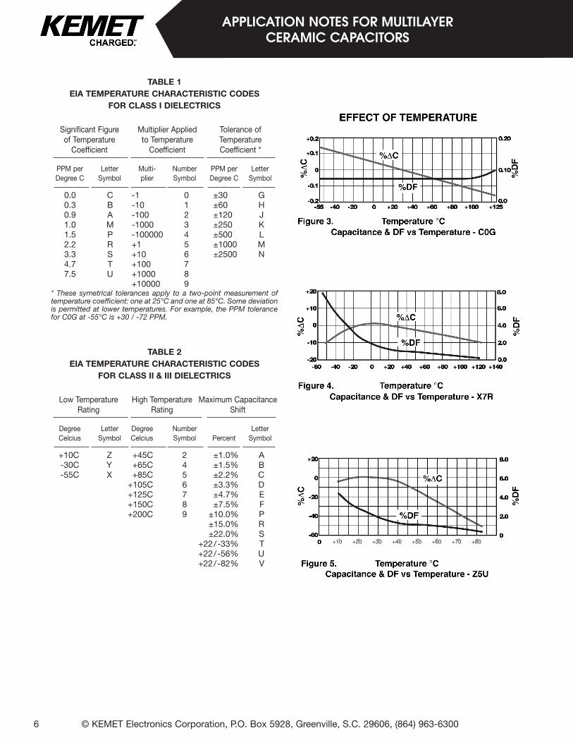
TABLE 1EIA TEMPERATURE CHARACTERISTIC CODES
FOR CLASS I DIELECTRICS
Significant Figure Multiplier Applied Tolerance ofof Temperature to Temperature Temperature
Coefficient Coefficient Coefficient *
PPM per Letter Multi- Number PPM per LetterDegree C Symbol plier Symbol Degree C Symbol
0.0 C -1 0 ±30 G0.3 B -10 1 ±60 H0.9 A -100 2 ±120 J1.0 M -1000 3 ±250 K1.5 P -100000 4 ±500 L2.2 R +1 5 ±1000 M3.3 S +10 6 ±2500 N4.7 T +100 77.5 U +1000 8
+10000 9* These symetrical tolerances apply to a two-point measurement oftemperature coefficient: one at 25°C and one at 85°C. Some deviationis permitted at lower temperatures. For example, the PPM tolerancefor C0G at -55°C is +30 / -72 PPM.
TABLE 2EIA TEMPERATURE CHARACTERISTIC CODES
FOR CLASS II & III DIELECTRICS
Low Temperature High Temperature Maximum CapacitanceRating Rating Shift
Degree Letter Degree Number LetterCelcius Symbol Celcius Symbol Percent Symbol
+10C Z +45C 2 ±1.0% A-30C Y +65C 4 ±1.5% B-55C X +85C 5 ±2.2% C
+105C 6 ±3.3% D+125C 7 ±4.7% E+150C 8 ±7.5% F+200C 9 ±10.0% P
±15.0% R±22.0% S
+22/-33% T+22/-56% U+22/-82% V
+10 +20 +30 +40 +50 +60 +70 +80
Effect of Temperature: Both capacitance and dissipa-tion factor are affected by variations in temperature. The max-imum capacitance change with temperature is defined by thetemperature characteristic. However, this only defines a “box”bounded by the upper and lower operating temperatures andthe minimum and maximum capacitance values. Within this“box”, the variation with temperature depends upon the spe-cific dielectric formulation. Typical curves for KEMET capaci-tors are shown in Figures 3, 4, and 5. These figures alsoinclude the typical change in dissipation factor for KEMETcapacitors.
Insulation resistance decreases with temperature.Typically, the insulation resistance at maximum rated temper-ature is 10% of the 25°C value.
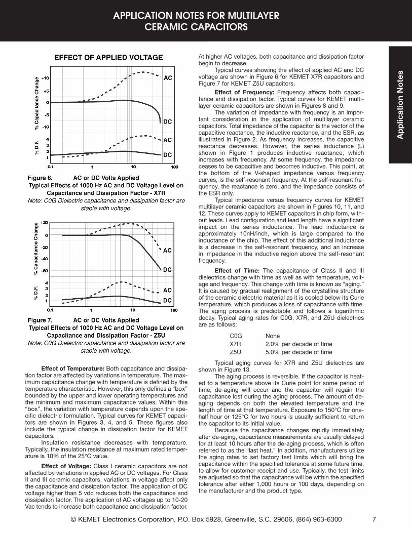
Effect of Voltage: Class I ceramic capacitors are notaffected by variations in applied AC or DC voltages. For ClassII and III ceramic capacitors, variations in voltage affect onlythe capacitance and dissipation factor. The application of DCvoltage higher than 5 vdc reduces both the capacitance anddissipation factor. The application of AC voltages up to 10-20Vac tends to increase both capacitance and dissipation factor.
At higher AC voltages, both capacitance and dissipation factorbegin to decrease.
Typical curves showing the effect of applied AC and DCvoltage are shown in Figure 6 for KEMET X7R capacitors andFigure 7 for KEMET Z5U capacitors.
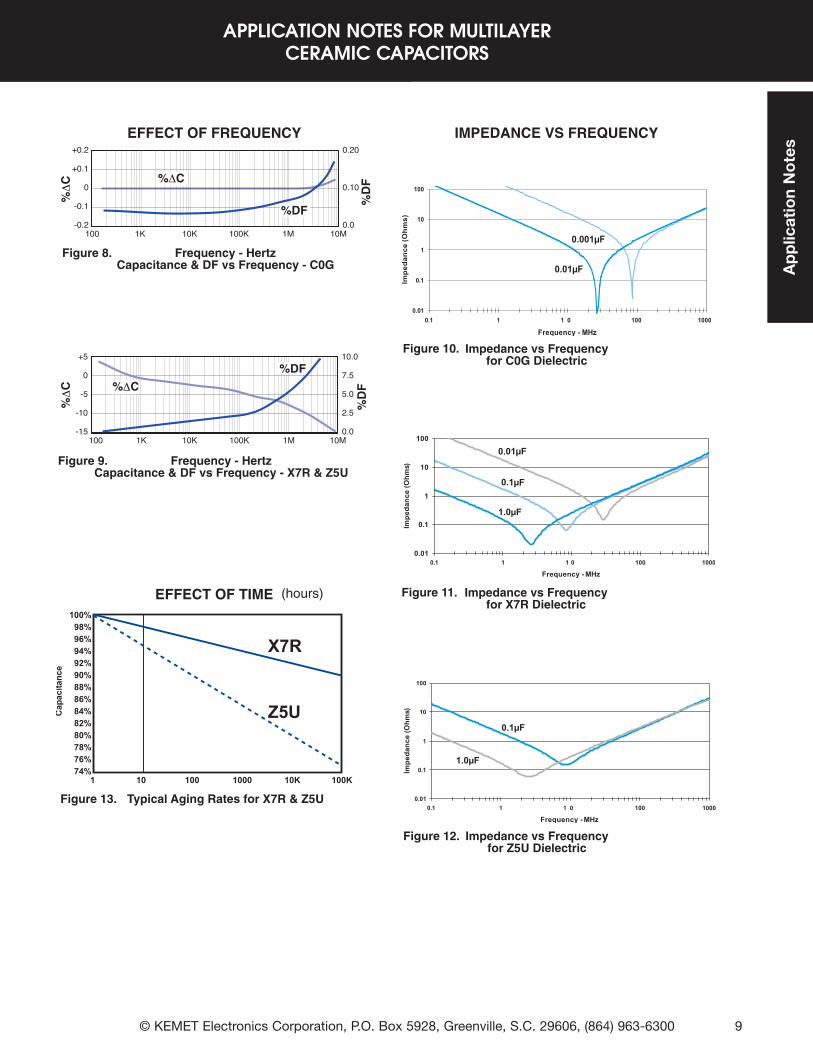
Effect of Frequency: Frequency affects both capaci-tance and dissipation factor. Typical curves for KEMET multi-layer ceramic capacitors are shown in Figures 8 and 9.
The variation of impedance with frequency is an impor-tant consideration in the application of multilayer ceramiccapacitors. Total impedance of the capacitor is the vector of thecapacitive reactance, the inductive reactance, and the ESR, asillustrated in Figure 2. As frequency increases, the capacitivereactance decreases. However, the series inductance (L)shown in Figure 1 produces inductive reactance, whichincreases with frequency. At some frequency, the impedanceceases to be capacitive and becomes inductive. This point, atthe bottom of the V-shaped impedance versus frequencycurves, is the self-resonant frequency. At the self-resonant fre-quency, the reactance is zero, and the impedance consists ofthe ESR only.
Typical impedance versus frequency curves for KEMETmultilayer ceramic capacitors are shown in Figures 10, 11, and12. These curves apply to KEMET capacitors in chip form, with-out leads. Lead configuration and lead length have a significantimpact on the series inductance. The lead inductance isapproximately 10nH/inch, which is large compared to theinductance of the chip. The effect of this additional inductanceis a decrease in the self-resonant frequency, and an increasein impedance in the inductive region above the self-resonantfrequency.
Effect of Time: The capacitance of Class II and IIIdielectrics change with time as well as with temperature, volt-age and frequency. This change with time is known as “aging.”It is caused by gradual realignment of the crystalline structureof the ceramic dielectric material as it is cooled below its Curietemperature, which produces a loss of capacitance with time.The aging process is predictable and follows a logarithmicdecay. Typical aging rates for C0G, X7R, and Z5U dielectrics are as follows:
C0G NoneX7R 2.0% per decade of timeZ5U 5.0% per decade of time
Typical aging curves for X7R and Z5U dielectrics areshown in Figure 13.
The aging process is reversible. If the capacitor is heat-ed to a temperature above its Curie point for some period oftime, de-aging will occur and the capacitor will regain thecapacitance lost during the aging process. The amount of de-aging depends on both the elevated temperature and thelength of time at that temperature. Exposure to 150°C for one-half hour or 125°C for two hours is usually sufficient to returnthe capacitor to its initial value.
Because the capacitance changes rapidly immediatelyafter de-aging, capacitance measurements are usually delayedfor at least 10 hours after the de-aging process, which is oftenreferred to as the “last heat.” In addition, manufacturers utilizethe aging rates to set factory test limits which will bring thecapacitance within the specified tolerance at some future time,to allow for customer receipt and use. Typically, the test limitsare adjusted so that the capacitance will be within the specifiedtolerance after either 1,000 hours or 100 days, depending onthe manufacturer and the product type.
© KEMET Electronics Corporation, P.O. Box 5928, Greenville, S.C. 29606, (864) 963-6300 7
Ap
plic
atio
nN
ote
s
APPLICATION NOTES FOR MULTILAYER CERAMIC CAPACITORS
APPLICATION NOTES FOR MULTILAYER CERAMIC CAPACITORS
© KEMET Electronics Corporation, P.O. Box 5928, Greenville, S.C. 29606, (864) 963-63008
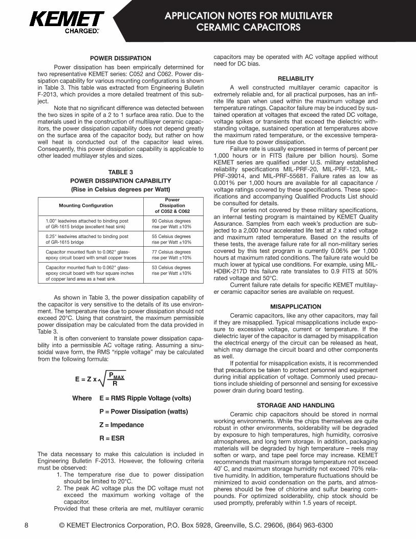
POWER DISSIPATIONPower dissipation has been empirically determined for
two representative KEMET series: C052 and C062. Power dis-sipation capability for various mounting configurations is shownin Table 3. This table was extracted from Engineering BulletinF-2013, which provides a more detailed treatment of this sub-ject.
Note that no significant difference was detected betweenthe two sizes in spite of a 2 to 1 surface area ratio. Due to thematerials used in the construction of multilayer ceramic capac-itors, the power dissipation capability does not depend greatlyon the surface area of the capacitor body, but rather on howwell heat is conducted out of the capacitor lead wires.Consequently, this power dissipation capability is applicable toother leaded multilayer styles and sizes.
TABLE 3POWER DISSIPATION CAPABILITY(Rise in Celsius degrees per Watt)
PowerMounting Configuration Dissipation
of C052 & C062
1.00" leadwires attached to binding post 90 Celsius degreesof GR-1615 bridge (excellent heat sink) rise per Watt ±10%
0.25" leadwires attached to binding post 55 Celsius degreesof GR-1615 bridge rise per Watt ±10%
Capacitor mounted flush to 0.062" glass- 77 Celsius degreesepoxy circuit board with small copper traces rise per Watt ±10%
Capacitor mounted flush to 0.062" glass- 53 Celsius degreesepoxy circuit board with four square inches rise per Watt ±10%of copper land area as a heat sink
As shown in Table 3, the power dissipation capability ofthe capacitor is very sensitive to the details of its use environ-ment. The temperature rise due to power dissipation should notexceed 20°C. Using that constraint, the maximum permissiblepower dissipation may be calculated from the data provided inTable 3.
It is often convenient to translate power dissipation capa-bility into a permissible AC voltage rating. Assuming a sinu-soidal wave form, the RMS “ripple voltage” may be calculated
The data necessary to make this calculation is included inEngineering Bulletin F-2013. However, the following criteriamust be observed:
1. The temperature rise due to power dissipationshould be limited to 20°C.
2. The peak AC voltage plus the DC voltage must notexceed the maximum working voltage of thecapacitor.
Provided that these criteria are met, multilayer ceramic
E = Z x
Where E = RMS Ripple Voltage (volts)
P = Power Dissipation (watts)
Z = Impedance
R = ESR
PMAXR
capacitors may be operated with AC voltage applied withoutneed for DC bias.
RELIABILITYA well constructed multilayer ceramic capacitor is
extremely reliable and, for all practical purposes, has an infi-nite life span when used within the maximum voltage andtemperature ratings. Capacitor failure may be induced by sus-tained operation at voltages that exceed the rated DC voltage,voltage spikes or transients that exceed the dielectric with-standing voltage, sustained operation at temperatures abovethe maximum rated temperature, or the excessive tempera-ture rise due to power dissipation.
Failure rate is usually expressed in terms of percent per1,000 hours or in FITS (failure per billion hours). SomeKEMET series are qualified under U.S. military establishedreliability specifications MIL-PRF-20, MIL-PRF-123, MIL-PRF-39014, and MIL-PRF-55681. Failure rates as low as0.001% per 1,000 hours are available for all capacitance /voltage ratings covered by these specifications. These spec-ifications and accompanying Qualified Products List shouldbe consulted for details.
For series not covered by these military specifications,an internal testing program is maintained by KEMET QualityAssurance. Samples from each week’s production are sub-jected to a 2,000 hour accelerated life test at 2 x rated voltageand maximum rated temperature. Based on the results ofthese tests, the average failure rate for all non-military seriescovered by this test program is currently 0.06% per 1,000hours at maximum rated conditions. The failure rate would bemuch lower at typical use conditions. For example, using MIL-HDBK-217D this failure rate translates to 0.9 FITS at 50%rated voltage and 50°C.
Current failure rate details for specific KEMET multilay-er ceramic capacitor series are available on request.
MISAPPLICATIONCeramic capacitors, like any other capacitors, may fail
if they are misapplied. Typical misapplications include expo-sure to excessive voltage, current or temperature. If thedielectric layer of the capacitor is damaged by misapplicationthe electrical energy of the circuit can be released as heat,which may damage the circuit board and other componentsas well.
If potential for misapplication exists, it is recommendedthat precautions be taken to protect personnel and equipmentduring initial application of voltage. Commonly used precau-tions include shielding of personnel and sensing for excessivepower drain during board testing.
STORAGE AND HANDLINGCeramic chip capacitors should be stored in normal
working environments. While the chips themselves are quiterobust in other environments, solderability will be degradedby exposure to high temperatures, high humidity, corrosiveatmospheres, and long term storage. In addition, packagingmaterials will be degraded by high temperature – reels maysoften or warp, and tape peel force may increase. KEMETrecommends that maximum storage temperature not exceed40˚ C, and maximum storage humidity not exceed 70% rela-tive humidity. In addition, temperature fluctuations should beminimized to avoid condensation on the parts, and atmos-pheres should be free of chlorine and sulfur bearing com-pounds. For optimized solderability, chip stock should beused promptly, preferably within 1.5 years of receipt.
from the following formula:
IMPEDANCE VS FREQUENCY
Imp
edan
ce(O
hm
s)
1 10 100 1,0000.001
0.01
1
10
100
0.1
0.1
Frequency - MHzImpedance vs Frequency for C0G Dielectric
Figure 10.
EFFECT OF FREQUENCY
-0.1
0
+0.2
-0.2
+0.1
0.10
0.20
0.0
Frequency - HertzCapacitance & DF vs Frequency - C0G
Figure 8.
%D
F
Typical Aging Rates for X7R & Z5UFigure 13.
74%76%78%80%82%84%86%88%90%92%94%96%98%
100%
Cap
acit
ance
1 10 100 1000 10K 100K
EFFECT OF TIME
%D
F
-10
-5
+5
-15
0
5.0
10.0
0.0
2.5
7.5
Frequency - HertzCapacitance & DF vs Frequency - X7R & Z5U
Figure 9.
.01μF .001μF
%Δ
C
100 1K 10K 100K 1M 10M
100 1K 10K 100K 1M 10M
%Δ
C %ΔC
%DF
Z5U
X7R
%DF
%ΔC
Imp
edan
ce(O
hm
s)
1 10 100 1,0000.001
0.01
1
10
100
0.1
0.1
Frequency - MHzImpedance vs Frequency for Z5U Dielectric
Figure 12.
Imp
edan
ce(O
hm
s)
1 10 100 1,0000.001
0.01
1
10
100
0.1
0.1
Frequency - MHzImpedance vs Frequency for X7R Dielectric
Figure 11.
0.1μF
1.0 μF
0.1μF .01μF
1.0 μF
Impedance vs. Frequency
Leaded Ceramic C0G
0.01
0.1
1
10
100
0.1 1 1 0 100 1000
Frequency - MHz
Imp
ed
an
ce
(Oh
ms
)
0.01µF
0.001µF
Leaded X7R
0.01
0.1
1
10
100
0.1 1 1 0 100 1000
Frequency - MHz
Imp
ed
an
ce
(Oh
ms)
0.01µF
0.1µF
Impedance vs. Frequency
1.0µF
Impedance vs. FrequencyLeaded Z5U
0.01
0.1
1
10
100
0.1 1 1 0 100 1000
Frequency - MHz
Imp
ed
an
ce
(Oh
ms)
0.1µF
1.0µF
Impedance vs Frequencyfor C0G Dielectric
Figure 10.
Impedance vs Frequencyfor Z5U Dielectric
Figure 12.
Impedance vs Frequencyfor X7R Dielectric
Figure 11.
Impedance vs Frequencyfor C0G Dielectric
Figure 10.
Impedance vs Frequencyfor Z5U Dielectric
Figure 12.
Impedance vs Frequencyfor X7R Dielectric
Figure 11.
Impedance vs Frequencyfor C0G Dielectric
Figure 10.
Impedance vs Frequencyfor Z5U Dielectric
Figure 12.
Impedance vs Frequencyfor X7R Dielectric
Figure 11.
���
�����
���
�
� ������������� ������������� �������
���
���
� �
© KEMET Electronics Corporation, P.O. Box 5928, Greenville, S.C. 29606, (864) 963-6300 9
Ap
plic
atio
nN
ote
s
APPLICATION NOTES FOR MULTILAYER CERAMIC CAPACITORS
Impedance vs Frequencyfor C0G Dielectric
Figure 10.
Impedance vs Frequencyfor Z5U Dielectric
Figure 12.
Impedance vs Frequencyfor X7R Dielectric
Figure 11.
Impedance vs Frequencyfor C0G Dielectric
Figure 10.
Impedance vs Frequencyfor Z5U Dielectric
Figure 12.
Impedance vs Frequencyfor X7R Dielectric
Figure 11.
Impedance vs Frequencyfor C0G Dielectric
Figure 10.
Impedance vs Frequencyfor Z5U Dielectric
Figure 12.
Impedance vs Frequencyfor X7R Dielectric
Figure 11.
(hours)