òÔ ' Âæhe¼8 Ï,éÕ râß¿$ ~=6w tp pô gñÊ®¬â/ µùÏoÔ oÑÖ jy¤q ... · title:...
TRANSCRIPT

To learn more about ON Semiconductor, please visit our website at www.onsemi.com
Please note: As part of the Fairchild Semiconductor integration, some of the Fairchild orderable part numbers will need to change in order to meet ON Semiconductor’s system requirements. Since the ON Semiconductor product management systems do not have the ability to manage part nomenclature that utilizes an underscore (_), the underscore (_) in the Fairchild part numbers will be changed to a dash (-). This document may contain device numbers with an underscore (_). Please check the ON Semiconductor website to verify the updated device numbers. The most current and up-to-date ordering information can be found at www.onsemi.com. Please email any questions regarding the system integration to [email protected].
Is Now Part of
ON Semiconductor and the ON Semiconductor logo are trademarks of Semiconductor Components Industries, LLC dba ON Semiconductor or its subsidiaries in the United States and/or other countries. ON Semiconductor owns the rights to a number of patents, trademarks, copyrights, trade secrets, and other intellectual property. A listing of ON Semiconductor’s product/patent coverage may be accessed at www.onsemi.com/site/pdf/Patent-Marking.pdf. ON Semiconductor reserves the right to make changes without further notice to any products herein. ON Semiconductor makes no warranty, representation or guarantee regarding the suitability of its products for any particular purpose, nor does ON Semiconductor assume any liability arising out of the application or use of any product or circuit, and specifically disclaims any and all liability, including without limitation special, consequential or incidental damages. Buyer is responsible for its products and applications using ON Semiconductor products, including compliance with all laws, regulations and safety requirements or standards, regardless of any support or applications information provided by ON Semiconductor. “Typical” parameters which may be provided in ON Semiconductor data sheets and/or specifications can and do vary in different applications and actual performance may vary over time. All operating parameters, including “Typicals” must be validated for each customer application by customer’s technical experts. ON Semiconductor does not convey any license under its patent rights nor the rights of others. ON Semiconductor products are not designed, intended, or authorized for use as a critical component in life support systems or any FDA Class 3 medical devices or medical devices with a same or similar classification in a foreign jurisdiction or any devices intended for implantation in the human body. Should Buyer purchase or use ON Semiconductor products for any such unintended or unauthorized application, Buyer shall indemnify and hold ON Semiconductor and its officers, employees, subsidiaries, affiliates, and distributors harmless against all claims, costs, damages, and expenses, and reasonable attorney fees arising out of, directly or indirectly, any claim of personal injury or death associated with such unintended or unauthorized use, even if such claim alleges that ON Semiconductor was negligent regarding the design or manufacture of the part. ON Semiconductor is an Equal Opportunity/Affirmative Action Employer. This literature is subject to all applicable copyright laws and is not for resale in any manner.

March 2012
© 2009 Fairchild Semiconductor Corporation www.fairchildsemi.com FXLA101 • Rev. 1.0.4
FL
XA
101 — L
ow
-Vo
ltage D
ual-S
up
ply 1-B
it Vo
ltage T
ranslato
r with
Au
to D
irection
Sen
sing
FXLA101 Low-Voltage Dual-Supply 1-Bit Voltage Translator with Auto Direction Sensing
Features
Bi-Directional Interface between Two Levels: from 1.1V to 3.6V
Fully Configurable: Inputs and Outputs Track VCC
Non-Preferential Power-Up; Either VCC May Be Powered Up First
Outputs Switch to 3-State if Either VCC is at GND
Power-Off Protection
Bus-Hold on Data Inputs Eliminates the Need for Pull-Up Resistors; Do Not Use Pull-Up Resistors on A or B Ports
Control Input (/OE) Referenced to VCCA Voltage
Packaged in MicroPak™ 6 (1.00mm x 1.45mm)
Direction Control Not Necessary
100Mbps Throughput when Translating Between 1.8V and 2.5V
ESD Protection Exceeds:
- 8kV HBM (per JESD22-A114 & Mil Std 883e 3015.7)
- 2kV CDM (per ESD STM 5.3)
Applications
Cell Phones, PDAs, Digital Cameras, Portable GPS
Description
The FXLA101 is a configurable dual-voltage supply translator for both uni-directional and bi-directional voltage translation between two logic levels. The device allows translation between voltages as high as 3.6V to as low as 1.1V. The A port tracks the VCCA level and the B port tracks the VCCB level. This allows for bi-directional voltage translation over a variety of voltage levels: 1.2V, 1.5V, 1.8V, 2.5V, and 3.3V.
The device remains in three-state as long as either VCC=0V, allowing either VCC to be powered up first. Internal power-down control circuits place the device in 3-state if either VCC is removed.
The /OE input, when HIGH, disables both the A and B ports by placing them in a 3-state condition. The /OE input is supplied by VCCA.
The FXLA101 supports bi-directional translation without the need for a direction control pin. The two ports of the device have auto-direction sense capability. Either port may sense an input signal and transfer it as an output signal to the other port.
Ordering Information
Part Number Top Mark
Operating Temperature
Range Package
Packing Method
FXLA101L6X XK -40 to 85°C
6-Lead MicroPak™1.00mm x 1.45mm Package 5K Units Tape and Reel FXLA101FHX XK 6-Lead, MicroPak2™, 1x1mm Body, .35mm Pitch

© 2009 Fairchild Semiconductor Corporation www.fairchildsemi.com FLXA101 • Rev. 1.0.4 2
FL
XA
101 — L
ow
-Vo
ltage D
ual-S
up
ply 1-B
it Vo
ltage T
ranslato
r with
Au
to D
irection
Sen
sing
Pin Configuration
Figure 1. Pin Configuration (Top Through View)
Pin Definitions
Pin # Name Description
1 VCCA A-Side Power Supply
2 GND Ground
3 A A Side Input or 3-State Output
4 B B Side Input or 3-State Output
5 /OE Output Enable Input
6 VCCB B Side Power supply

© 2009 Fairchild Semiconductor Corporation www.fairchildsemi.com FLXA101 • Rev. 1.0.4 3
FL
XA
101 — L
ow
-Vo
ltage D
ual-S
up
ply 1-B
it Vo
ltage T
ranslato
r with
Au
to D
irection
Sen
sing
Functional Diagram
Figure 2. Functional Diagram
Function Table
Control Outputs
/OE
L Normal Operation
H 3-State
H = HIGH Logic Level
L = LOW Logic Level

© 2009 Fairchild Semiconductor Corporation www.fairchildsemi.com FLXA101 • Rev. 1.0.4 4
FL
XA
101 — L
ow
-Vo
ltage D
ual-S
up
ply 1-B
it Vo
ltage T
ranslato
r with
Au
to D
irection
Sen
sing
Absolute Maximum Ratings
Stresses exceeding the absolute maximum ratings may damage the device. The device may not function or be operable above the recommended operating conditions and stressing the parts to these levels is not recommended. In addition, extended exposure to stresses above the recommended operating conditions may affect device reliability. The absolute maximum ratings are stress ratings only.
Symbol Parameter Conditions Min. Max. Unit
VCC Supply Voltage VCCA -0.5 4.6
V VCCB -0.5 4.6
VI DC Input Voltage I/O Ports A and B -0.5 4.6
V Control Input (/OE) -0.5 4.6
VO Output Voltage(2)
Output 3-State -0.5 4.6
V Output Active (An) -0.5 VCCA +0.5
Output Active (Bn) -0.5 VCCB +0.5
IIK DC Input Diode Current VI<0V -50 mA
IOK DC Output Diode Current VO<0V -50
mA VO>VCC +50
IOH/IOL DC Output Source/Sink Current -50 +50 mA
ICC DC VCC or Ground Current (per Supply Pin) ±100 mA
TSTG Storage Temperature Range -65 +150 °C
PD Power Dissipation 4.5 mW
ESD Human Body Model, JESD22-A114
B Port I/O to GND 12
kV A Port I/O to GND 8
Charged Device Model, JESD22-C101 2
Notes: 1. IO absolute maximum ratings must be observed. 2. All unused inputs and input/outputs must be held at VCCi or GND.
Recommended Operating Conditions
The Recommended Operating Conditions table defines the conditions for actual device operation. Recommended operating conditions are specified to ensure optimal performance to the datasheet specifications. Fairchild does not recommend exceeding them or designing to Absolute Maximum Ratings.
Symbol Parameter Conditions Min. Max. Unit
VCC Power Supply Operating VCCA or VCCB 1.1 3.6 V
VIN Input Voltage Ports A and B 0 3.6 V
Control Input (/OE) 0 VCCA V
TA Operating Temperature, Free Air -40 +85 °C
dt/dV Minimum Input Edge Rate VCCA/B = 1.1 to 3.6V 10 ns/V
ΘJA Thermal Resistance Micropak-6 350
°C/W Micropak2-6 560

© 2009 Fairchild Semiconductor Corporation www.fairchildsemi.com FLXA101 • Rev. 1.0.4 5
FL
XA
101 — L
ow
-Vo
ltage D
ual-S
up
ply 1-B
it Vo
ltage T
ranslato
r with
Au
to D
irection
Sen
sing
Power-Up/Power-Down Sequence
FXL translators offer an advantage in that either VCC may be powered up first. This benefit derives from the chip design. When either VCC is at 0V, outputs are in a high-impedance state. The control input (/OE) is designed to track the VCCA supply. A pull-up resistor tying /OE to VCCA should be used to ensure that bus contention, excessive currents, or oscillations do not occur during power-up or power-down. The size of the pull-up resistor is based upon the current-sinking capability of the device driving the /OE pin.
The recommended power-up sequence is:
1. Apply power to the first VCC. 2. Apply power to the second VCC. 3. Drive the /OE input LOW to enable the device.
The recommended power-down sequence is:
1. Drive /OE input HIGH to disable the device. 2. Remove power from either VCC. 3. Remove power from other VCC.
Pull-Up/Pull-Down Resistors Do not use pull-up or pull-down resistors. This device has bus-hold circuits: pull-up or pull-down resistors are not recommended because they interfere with the output state. The current through these resistors may exceed the hold drive, II(HOLD) and/or II(OD) bus-hold currents. The bus-hold feature eliminates the need for extra resistors.

© 2009 Fairchild Semiconductor Corporation www.fairchildsemi.com FLXA101 • Rev. 1.0.4 6
FL
XA
101 — L
ow
-Vo
ltage D
ual-S
up
ply 1-B
it Vo
ltage T
ranslato
r with
Au
to D
irection
Sen
sing
DC Electrical Characteristics
TA=-40 to 85°C.
Symbol Parameter Conditions VCCA (V) VCCB (V) Min. Typ. Max. Units
VIHA
High-Level Input Voltage
Data Inputs An Control Pin /OE
2.70 to 3.60
1.10 to 3.60
2.00
V
2.30 to 2.70 1.60
1.65 to 2.30 .65xVCCA
1.40 to 1.65 .65xVCCA
1.10 to 1.40 .90xVCCA
VIHB Data Inputs Bn 1.10 to 3.60
2.70 to 3.60 2.00
V
2.30 to 2.70 1.60
1.65 to 2.30 .65xVCCB
1.40 to 1.65 .65xVCCB
1.10 to 1.40 .90xVCCB
VILA
Low-Level Input Voltage
Data Inputs An Control Pin /OE
2.70 to 3.60
1.10 to 3.60
.80
V
2.30 to 2.70 .70
1.65 to 2.30 .35xVCCA
1.40 to 1.65 .35xVCCA
1.10 to 1.40 .10xVCCA
VILB Data Inputs Bn 1.10 to 3.60
2.70 to 3.60 .80
V
2.30 to 2.70 .70
1.65 to 2.30 .35xVCCB
1.40 to 1.65 .35xVCCB
1.10 to 1.40 .10xVCCB
VOHA High-Level Output Voltage(3)
IOH=-4µA 1.10 to 3.60 1.10 to 3.60 VCCA - .40 V
VOHB IOH=-4µA 1.10 to 3.60 1.10 to 3.60 VCCB - .40
VOLA Low-Level Output Voltage(3)
IOL=4µA 1.10 to 3.60 1.10 to 3.60 .4 V
VOLB IOL=4µA 1.10 to 3.60 1.10 to 3.60 .4
II(HOLD) Bus-Hold Input Minimum Drive Current
VIN=0.80V 3.00 3.00 75.0
µA
VIN=2.00V 3.00 3.00 -75.0
VIN=0.7V 2.30 2.30 45.0
VIN=1.60V 2.30 2.30 -45.0
VIN=0.57V 1.65 1.65 25.0
VIN=1.07V 1.65 1.65 -25.0
VIN=0.49V 1.40 1.40 11.0
VIN=0.91V 1.40 1.40 -11.0
VIN=0.11V 1.10 1.10 4.0
VIN=0.99V 1.10 1.10 -4.0
Continued on following page…

© 2009 Fairchild Semiconductor Corporation www.fairchildsemi.com FLXA101 • Rev. 1.0.4 7
FL
XA
101 — L
ow
-Vo
ltage D
ual-S
up
ply 1-B
it Vo
ltage T
ranslato
r with
Au
to D
irection
Sen
sing
DC Electrical Characteristics (Continued)
TA=-40 to 85°C.
Symbol Parameter Conditions VCCA (V) VCCB (V) Min. Max. Units
II(ODH) Bus-Hold Input Overdrive High Current(4)
Data Inputs An, Bn
3.60 3.60 450.00
µA
2.70 2.70 300.00
1.95 1.95 200.00
1.60 1.60 120.00
1.40 1.40 80.00
II(ODL) Bus-Hold Input Overdrive Low Current(5)
Data Inputs An, Bn
3.60 3.60 -450.00
µA
2.70 2.70 -300.00
1.95 1.95 -200.00
1.60 1.60 -120.00
1.40 1.40 -80.00
II Input Leakage Current Control Inputs /OE, VI=VCCA or GND
1.10 to 3.60 3.60 ±1.0 µA
IOFF Power-Off Leakage Current
An VO=0V to 3.6V 0 3.6 ±2.0 µA
Bn VO=0V to 3.6V 3.60 0 ±2.0
IOZ 3-State Output Leakage
An, Bn VO=0V or 3.6V, /OE=VIH
3.6 3.60 ±5.0
µA An VO=0V or 3.6V, /OE=GND
3.60 0 ±5.0
Bn VO=0V or 3.6V, /OE=GND
0 3.60 ±5.0
ICCA/B Quiescent Supply Current(6, 7)
VI=VCCI or GND; IO=0, /OE=GND
1.10 to 3.60 1.10 to 3.60 10.0 µA
ICCZ VI=VCCI or GND; IO=0, /OE=VIH
1.10 to 3.60 1.10 to 3.60 10.0 µA
ICCA
Quiescent Supply Current
VI=VCCB or GND; IO=0 B-to-A Direction, /OE=GND
0 1.10 to 3.60 -10.0
µA VI=VCCA or GND; IO=0 A-to-B Direction
1.10 to 3.60 0 10.0
ICCB
VI=VCCA or GND; IO=0, A-to-B Direction, /OE=GND
1.10 to 3.60 0 -10.0
µA VI=VCCB or GND; IO=0 B-to-A Direction
0 1.10 to 3.60 10.0
Notes: 3. This is the output voltage for static conditions. Dynamic drive specifications are given in the Dynamic Output
Electrical Characteristics table. 4. An external drive must source at least the specified current to switch LOW-to-HIGH. 5. An external drive must source at least the specified current to switch HIGH-to-LOW. 6. VCCI is the VCC associated with the input side. 7. Reflects current per supply, VCCA or VCCB.

© 2009 Fairchild Semiconductor Corporation www.fairchildsemi.com FLXA101 • Rev. 1.0.4 8
FL
XA
101 — L
ow
-Vo
ltage D
ual-S
up
ply 1-B
it Vo
ltage T
ranslato
r with
Au
to D
irection
Sen
sing
Dynamic Output Electrical Characteristic
A Port (An)
Output Load: CL=15pF, RL ≥ MΩ (CI/O=4pF), TA=-40 to 85°C
Symbol Parameter
VCCA=3.0V to 3.6V
VCCA=2.3V to 2.7V
VCCA=1.65V to 1.95V
VCCA=1.4V to 1.6V
VCCA=1.1V to 1.3V Units
Typ. Max. Typ. Max. Typ. Max Typ. Max. Typ.
trise Output Rise Time A Port(9)
3.0 3.5 4.0 5.0 7.5 ns
tfall Output Fall Time A Port(10)
3.0 3.5 4.0 5.0 7.5 ns
IOHD
Dynamic Output Current High(9)
-11.4 -7.5 -4.7 -3.2 -1.7 mA
IOLD
Dynamic Output Current Low(10)
+11.4 +7.5 +4.7 +3.2 +1.7 mA
B Port (Bn)
Output Load: CL=15pF, RL ≥ MΩ (CI/O=5pF), TA=-40 to 85°C
Symbol Parameter
VCCB=3.0V to 3.6V
VCCB=2.3V to 2.7V
VCCB=1.65V to 1.95V
VCCB=1.4V to 1.6V
VCCB=1.1V to 1.3V Units
Typ. Max. Typ. Max. Typ. Max Typ. Max. Typ.
trise Output Rise Time B Port(9)
3.0 3.5 4.0 5.0 7.5 ns
tfall Output Fall Time B Port(10)
3.0 3.5 4.0 5.0 7.5 ns
IOHD
Dynamic Output Current High(9)
-12.0 -7.9 -5.0 -3.4 -1.8 mA
IOLD
Dynamic Output Current Low(10)
+12.0 +7.9 +5.0 +3.4 +1.8 mA
Notes: 8. Dynamic output characteristics are guaranteed, but not tested. 9. See Figure 7. 10. See Figure 8.

© 2009 Fairchild Semiconductor Corporation www.fairchildsemi.com FLXA101 • Rev. 1.0.4 9
FL
XA
101 — L
ow
-Vo
ltage D
ual-S
up
ply 1-B
it Vo
ltage T
ranslato
r with
Au
to D
irection
Sen
sing
AC Characteristics
VCCA = 3.0V to 3.6V, TA=-40 to 85°C
Symbol Parameter
VCCB=3.0V to 3.6V
VCCB=2.3V to 2.7V
VCCB=1.65V to 1.95V
VCCB=1.4V to 1.6V
VCCB=1.1V to 1.3V Units
Min. Max. Min. Max. Min. Max Min. Max. Typ.
tPLH,tPHL A to B 0.2 4.0 0.3 4.2 0.5 5.4 0.6 6.8 6.9 ns
B to A 0.2 4.0 0.2 4.1 0.3 5.0 0.5 6.0 4.5 ns
tPZL,tPZH /OE to A, /OE to B
1.7 1.7 1.7 1.7 1.7 µs
tSKEW A Port, B Port(11)
0.5 0.5 0.5 1.0 1.0 ns
VCCA = 2.3V to 2.7V, TA=-40 to 85°C
Symbol Parameter
VCCB=3.0V to 3.6V
VCCB=2.3V to 2.7V
VCCB=1.65V to 1.95V
VCCB=1.4V to 1.6V
VCCB=1.1V to 1.3V Units
Min. Max. Min. Max. Min. Max Min. Max. Typ.
tPLH,tPHL A to B 0.2 4.1 0.4 4.5 0.5 5.6 0.8 6.9 7.0 ns
B to A 0.3 4.2 0.4 4.5 0.5 5.5 0.5 6.5 4.8 ns
tPZL,tPZH /OE to A, /OE to B
1.7 1.7 1.7 1.7 1.7 µs
tSKEW A Port, B Port(11)
0.5 0.5 0.5 1.0 1.0 ns
VCCA = 1.65V to 1.95V, TA=-40 to 85°C
Symbol Parameter
VCCB=3.0V to 3.6V
VCCB=2.3V to 2.7V
VCCB=1.65V to 1.95V
VCCB=1.4V to 1.6V
VCCB=1.1V to 1.3V Units
Min. Max. Min. Max. Min. Max Min. Max. Typ.
tPLH,tPHL A to B 0.3 5.0 0.5 5.5 0.8 6.7 0.9 7.5 7.5 ns
B to A 0.5 5.4 0.5 5.6 0.8 6.7 1.0 7.0 5.4 ns
tPZL,tPZH /OE to A, /OE to B
1.7 1.7 1.7 1.7 1.7 µs
tSKEW A Port, B Port(11)
0.5 0.5 0.5 1.0 1.0 ns
Note: 11. Skew is the variation of propagation delay between output signals and applies only to output signals on the same
port (An or Bn) and switching with the same polarity (LOW-to-HIGH or HIGH-to-LOW) (see Figure 10). Skew is guaranteed, but not tested.

© 2009 Fairchild Semiconductor Corporation www.fairchildsemi.com FLXA101 • Rev. 1.0.4 10
FL
XA
101 — L
ow
-Vo
ltage D
ual-S
up
ply 1-B
it Vo
ltage T
ranslato
r with
Au
to D
irection
Sen
sing
AC Characteristics (Continued)
VCCA = 1.4V to 1.6V, TA=-40 to 85°C
Symbol Parameter
VCCB=3.0V to 3.6V
VCCB=2.3V to 2.7V
VCCB=1.65V to 1.95V
VCCB=1.4V to 1.6V
VCCB=1.1V to 1.3V Units
Min. Max. Min. Max. Min. Max Min. Max. Typ.
tPLH,tPHL A to B 0.5 6.0 0.5 6.5 1.0 7.0 1.0 8.5 7.9 ns
B to A 0.6 6.8 0.8 6.9 0.9 7.5 1.0 8.5 6.1 ns
tPZL,tPZH /OE to A, /OE to B
1.7 1.7 1.7 1.7 1.7 µs
tSKEW A Port, B Port(12)
1.0 1.0 1.0 1.0 1.0 ns
VCCA = 1.1V to 1.3V, TA=-40 to 85°C
Symbol Parameter
VCCB=3.0Vto 3.6V
VCCB=2.3Vto 2.7V
VCCB=1.65V to 1.95V
VCCB=1.4V to 1.6V
VCCB=1.1V to 1.3V Units
Typ. Typ. Typ. Typ. Typ.
tPLH,tPHL A to B 4.6 4.8 5.4 6.2 9.2 ns
B to A 6.8 7.0 7.4 7.8 9.1 ns
tPZL,tPZH /OE to A, /OE to B 1.7 1.7 1.7 1.7 1.7 µs
tSKEW A Port, B Port(12) 1.0 1.0 1.0 1.0 1.0 ns
Note: 12. Skew is the variation of propagation delay between output signals and applies only to output signals on the same
port (An or Bn) and switching with the same polarity (LOW-to-HIGH or HIGH-to-LOW) (see Figure 10). Skew is guaranteed, but not tested.
© 2009 Fairchild Semiconductor Corporation www.fairchildsemi.com FLXA101 • Rev. 1.0.4 11
FL
XA
101 — L
ow
-Vo
ltage D
ual-S
up
ply 1-B
it Vo
ltage T
ranslato
r with
Au
to D
irection
Sen
sing
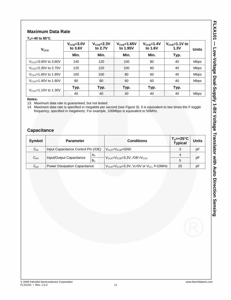
Maximum Data Rate
TA=-40 to 85°C.
VCCA
VCCB=3.0V to 3.6V
VCCB=2.3V to 2.7V
VCCB=1.65V to 1.95V
VCCB=1.4V to 1.6V
VCCB=1.1V to 1.3V Units
Min. Min. Min. Min. Typ.
VCCA=3.00V to 3.60V 140 120 100 80 40 Mbps
VCCA=2.30V to 2.70V 120 120 100 80 40 Mbps
VCCA=1.65V to 1.95V 100 100 80 60 40 Mbps
VCCA=1.40V to 1.60V 80 80 60 60 40 Mbps
VCCA=1.10V to 1.30V Typ. Typ. Typ. Typ. Typ.
40 40 40 40 40 Mbps
Notes: 13. Maximum data rate is guaranteed, but not tested. 14. Maximum data rate is specified in megabits per second (see Figure 9). It is equivalent to two times the F-toggle
frequency, specified in megahertz. For example, 100Mbps is equivalent to 50MHz.
Capacitance
Symbol Parameter Conditions TA=+25°C Typical
Units
CIN Input Capacitance Control Pin (/OE) VCCA=VCCB=GND 3 pF
CI/O Input/Output Capacitance An
VCCA=VCCB=3.3V, /OE=VCCA 4
pF Bn 5
Cpd Power Dissipation Capacitance VCCA=VCCB=3.3V, VI=0V or VCC, f=10MHz 25 pF

© 2009 Fairchild Semiconductor Corporation www.fairchildsemi.com FLXA101 • Rev. 1.0.4 12
FL
XA
101 — L
ow
-Vo
ltage D
ual-S
up
ply 1-B
it Vo
ltage T
ranslato
r with
Au
to D
irection
Sen
sing
I/O Architecture Benefit
The FXLA101 I/O architecture benefits the end user, beyond level translation, in the following three ways:
Auto Direction without an external direction pin.
Drive Capacitive Loads. Automatically shifts to a higher current drive mode only during “Dynamic Mode” or HL / LH transitions.
Lower Power Consumption. Automatically shifts to low-power mode during “Static Mode” (no transitions), lowering power consumption.
The FXLA101 does not require a direction pin. Instead, the I/O architecture detects input transitions on both side and automatically transfers the data to the corresponding output. For example, for a given channel, if both A and B side are at a static LOW, the direction has been established as A B, and a LH transition occurs on the B port; the FXLA101 internal I/O architecture automatically changes direction from A B to B A.
During HL / LH transitions, or “Dynamic Mode,” a strong output driver drives the output channel in parallel with a weak output driver. After a typical delay of approximately 10ns – 50ns, the strong driver is turned off, leaving the weak driver enabled for holding the logic state of the channel. This weak driver is called the “bus
hold.” “Static Mode” is when only the bus hold drives the channel. The bus hold can be over ridden in the event of a direction change. The strong driver allows the FXLA101 to quickly charge and discharge capacitive transmission lines during dynamic mode. Static mode conserves power, where ICC is typically < 5µA.
Bus Hold Minimum Drive Current Specifies the minimum amount of current the bus hold driver can source/sink. The bus hold minimum drive current (IIHOLD) is VCC dependent and guaranteed in the DC Electrical tables. The intent is to maintain a valid output state in a static mode, but that can be overridden when an input data transition occurs.
Bus Hold Input Overdrive Drive Current Specifies the minimum amount of current required (by an external device) to overdrive the bus hold in the event of a direction change. The bus hold overdrive (IIODH, IIODL) is VCC dependent and guaranteed in the DC Electrical tables.
Dynamic Output Current The strength of the output driver during LH / HL transitions is referenced on page 8, Dynamic Output Electrical Characteristics, IOHD, and IOLD.

© 2009 Fairchild Semiconductor Corporation www.fairchildsemi.com FLXA101 • Rev. 1.0.4 13
FL
XA
101 — L
ow
-Vo
ltage D
ual-S
up
ply 1-B
it Vo
ltage T
ranslato
r with
Au
to D
etection
Sen
sing
Test Diagrams
Figure 3. Test Circuit
Table 1. AC Test Conditions
Test Input Signal Output Enable Control
tPLH, tPHL Data Pulses 0V
tPZL 0V HIGH to LOW Switch
tPZH VCCI HIGH to LOW Switch
Table 2. AC Load
Figure 4. Waveform for Inverting and Non-Inverting Functions
Notes: 15. Input tR = tF = 2.0ns, 10% to 90%. 16. Input tR = tF = 2.5ns, 10% to 90%, at VI = 3.0V to 3.6V only.
VCC
DUT
C1 R1
TESTSIGNAL
VCCI
VCCO
GND
DATAIN
DATAOUT
tpxx tpxx
Vmi
Vmo
VCCO C1 R1
1.2V± 0.1V 15pF 1MΩ
1.5V± 0.1V 15pF 1MΩ
1.8V ± 0.15V 15pF 1MΩ
2.5V ± 0.2V 15pF 1MΩ
3.3V ± 0.3V 15pF 1MΩ

© 2009 Fairchild Semiconductor Corporation www.fairchildsemi.com FLXA101 • Rev. 1.0.4 14
FL
XA
101 — L
ow
-Vo
ltage D
ual-S
up
ply 1-B
it Vo
ltage T
ranslato
r with
Au
to D
etection
Sen
sing
Figure 5. 3-State Output Low Enable Time for Low Voltage Logic
Notes: 17. Input tR = tF = 2.0ns, 10% to 90%. 18. Input tR = tF = 2.5ns, 10% to 90%, at VI = 3.0V to 3.6V only.
Figure 6. 3-State Output High Enable Time for Low Voltage Logic
Notes: 19. Input tR = tF = 2.0ns, 10% to 90%. 20. Input tR = tF = 2.5ns, 10% to 90%, at VI = 3.0V to 3.6V only.
Table 3. Test Measure Points
Symbol VDD
VMI(21) VCCI /2
VMO VCCo /2
VX 0.9 x VCCo
VY 0.1 x VCCo
Note: 21. VCCI=VCCA for control pin /OE or VMI=(VCCA/2).

© 2009 Fairchild Semiconductor Corporation www.fairchildsemi.com FLXA101 • Rev. 1.0.4 15
FL
XA
101 — L
ow
-Vo
ltage D
ual-S
up
ply 1-B
it Vo
ltage T
ranslato
r with
Au
to D
etection
Sen
sing
RISE
CCOOIL
OUTOILOHD t
VCC
t
VCCI
•−×+=
ΔΔ
×+≈%)80%20(
)()( //
Figure 7. Active Output Rise Time and Dynamic Output Current High
FALL
CCOOIL
OUTOILOLD t
VCC
t
VCCI
•−×+=
ΔΔ
×+≈%)20%80(
)()( //
Figure 8. Active Output Fall Time and Dynamic Output Current Low
Figure 9. Maximum Data Rate
Figure 10. Output Skew Time
Note: 22. tSKEW = (tpHLmax – tpHLmin) or (tpLHmax – tpLHmin)
trise
80% x VCCO
20% x VCCO
VOH
VOL
VOUT
Time
tfall
80% x VCCO
20% x VCCOVOL
VOH
VOUT
Time
VCCIVCCI/2 VCCI/2
GND
DATAIN
tW
Maximum Data Rate, f = 1/tW
VCCOVmo
tskew tskew
VmoGND
DATAOUTPUT
VCCOVmo Vmo
GND
DATAOUTPUT

© 2009 Fairchild Semiconductor Corporation www.fairchildsemi.com FLXA101 • Rev. 1.0.4 16
FL
XA
101 — L
ow
-Vo
ltage D
ual-S
up
ply 1-B
it Vo
ltage T
ranslato
r with
Au
to D
etection
Sen
sing
Physical Dimensions
Figure 11. 6-Lead MicroPakTM 1.00mm x 1.45mm Package
Package drawings are provided as a service to customers considering Fairchild components. Drawings may change in any manner without notice. Please note the revision and/or date on the drawing and contact a Fairchild Semiconductor representative to verify or obtain the most recent revision. Package specifications do not expand the terms of Fairchild’s worldwide terms and conditions, specifically the warranty therein, which covers Fairchild products. Always visit Fairchild Semiconductor’s online packaging area for the most recent package drawings: http://www.fairchildsemi.com/packaging/.
2. DIMENSIONS ARE IN MILLIMETERS1. CONFORMS TO JEDEC STANDARD M0-252 VARIATION UAAD
4. FILENAME AND REVISION: MAC06AREV4
Notes:
3. DRAWING CONFORMS TO ASME Y14.5M-1994
TOP VIEW
RECOMMENEDLAND PATTERN
BOTTOM VIEW
1.45
1.00
A
B0.05 C
0.05 C
2X
2X
0.55MAX
0.05 C
(0.49)
(1)
(0.75)
(0.52)
(0.30)6X
1X
6X
PIN 1
DETAIL A
0.075 X 45CHAMFER
0.250.15
0.350.25
0.400.30
0.5(0.05)
1.0
5X
DETAIL APIN 1 TERMINAL
0.400.30
0.450.350.10
0.00
0.10 C B A
0.05 C
C0.05 C
0.050.00
5X
5X
6X(0.13)4X
6X
PIN 1 IDENTIFIER
(0.254)
5. PIN ONE IDENTIFIER IS 2X LENGTH OF ANY
5
OTHER LINE IN THE MARK CODE LAYOUT.

© 2009 Fairchild Semiconductor Corporation www.fairchildsemi.com FLXA101 • Rev. 1.0.4 17
FL
XA
101 — L
ow
-Vo
ltage D
ual-S
up
ply 1-B
it Vo
ltage T
ranslato
r with
Au
to D
etection
Sen
sing
Physical Dimensions
Figure 12. 6-Lead, MicroPak2, 1x1mm Body, .35mm Pitch
Package drawings are provided as a service to customers considering Fairchild components. Drawings may change in any manner without notice. Please note the revision and/or date on the drawing and contact a Fairchild Semiconductor representative to verify or obtain the most recent revision. Package specifications do not expand the terms of Fairchild’s worldwide terms and conditions, specifically the warranty therein, which covers Fairchild products. Always visit Fairchild Semiconductor’s online packaging area for the most recent package drawings: http://www.fairchildsemi.com/packaging/.
Tape and Reel Specification Please visit Fairchild Semiconductor’s online packaging area for the most recent tape and reel specifications: http://www.fairchildsemi.com/packaging/MicroPAK2_6L_tr.pdf.
Package Designator Tape Section Cavity Number Cavity Status Cover Type Status
FHX
Leader (Start End) 125 (Typical) Empty Sealed
Carrier 5000 Filled Sealed
Trailer (Hub End) 75 (Typical) Empty Sealed
1.00
B. DIMENSIONS ARE IN MILLIMETERS. C. DIMENSIONS AND TOLERANCES PER ASME Y14.5M, 1994
NOTES:
A. COMPLIES TO JEDEC MO-252 STANDARD
0.05 CAB
0.55MAX
0.05 C
C
0.35
0.090.191 2 3
0.350.25
5X
6XDETAIL A
0.60
(0.08)4X
(0.05) 6X
0.400.30
0.075X45°CHAMFER
5X 0.40
0.35
1X 0.45
6X 0.19
TOP VIEW
BOTTOM VIEW
0.66
0.10 C B A
.05 C
0.89
PIN 1
0.05 C
2X
2X 1.00
D. LANDPATTERN RECOMMENDATION IS BASED ON FSC
E. DRAWING FILENAME AND REVISION: MGF06AREV3
0.52
0.73
0.57
0.20 6X
1X
5X
RECOMMENDED LAND PATTERN
FOR SPACE CONSTRAINED PCB
DETAIL APIN 1 LEAD SCALE: 2X
ALTERNATIVE LAND PATTERN
FOR UNIVERSAL APPLICATION
DESIGN.
0.90
MIN 250uM
6 5 4
0.35
(0.08) 4X
SIDE VIEW

© 2009 Fairchild Semiconductor Corporation www.fairchildsemi.com FLXA101 • Rev. 1.0.4 18
FL
XA
101 — L
ow
-Vo
ltage D
ual-S
up
ply 1-B
it Vo
ltage T
ranslato
r with
Au
to D
etection
Sen
sing

www.onsemi.com1
ON Semiconductor and are trademarks of Semiconductor Components Industries, LLC dba ON Semiconductor or its subsidiaries in the United States and/or other countries.ON Semiconductor owns the rights to a number of patents, trademarks, copyrights, trade secrets, and other intellectual property. A listing of ON Semiconductor’s product/patentcoverage may be accessed at www.onsemi.com/site/pdf/Patent−Marking.pdf. ON Semiconductor reserves the right to make changes without further notice to any products herein.ON Semiconductor makes no warranty, representation or guarantee regarding the suitability of its products for any particular purpose, nor does ON Semiconductor assume any liabilityarising out of the application or use of any product or circuit, and specifically disclaims any and all liability, including without limitation special, consequential or incidental damages.Buyer is responsible for its products and applications using ON Semiconductor products, including compliance with all laws, regulations and safety requirements or standards,regardless of any support or applications information provided by ON Semiconductor. “Typical” parameters which may be provided in ON Semiconductor data sheets and/orspecifications can and do vary in different applications and actual performance may vary over time. All operating parameters, including “Typicals” must be validated for each customerapplication by customer’s technical experts. ON Semiconductor does not convey any license under its patent rights nor the rights of others. ON Semiconductor products are notdesigned, intended, or authorized for use as a critical component in life support systems or any FDA Class 3 medical devices or medical devices with a same or similar classificationin a foreign jurisdiction or any devices intended for implantation in the human body. Should Buyer purchase or use ON Semiconductor products for any such unintended or unauthorizedapplication, Buyer shall indemnify and hold ON Semiconductor and its officers, employees, subsidiaries, affiliates, and distributors harmless against all claims, costs, damages, andexpenses, and reasonable attorney fees arising out of, directly or indirectly, any claim of personal injury or death associated with such unintended or unauthorized use, even if suchclaim alleges that ON Semiconductor was negligent regarding the design or manufacture of the part. ON Semiconductor is an Equal Opportunity/Affirmative Action Employer. Thisliterature is subject to all applicable copyright laws and is not for resale in any manner.
PUBLICATION ORDERING INFORMATIONN. American Technical Support: 800−282−9855 Toll FreeUSA/Canada
Europe, Middle East and Africa Technical Support:Phone: 421 33 790 2910
Japan Customer Focus CenterPhone: 81−3−5817−1050
www.onsemi.com
LITERATURE FULFILLMENT:Literature Distribution Center for ON Semiconductor19521 E. 32nd Pkwy, Aurora, Colorado 80011 USAPhone: 303−675−2175 or 800−344−3860 Toll Free USA/CanadaFax: 303−675−2176 or 800−344−3867 Toll Free USA/CanadaEmail: [email protected]
ON Semiconductor Website: www.onsemi.com
Order Literature: http://www.onsemi.com/orderlit
For additional information, please contact your localSales Representative
© Semiconductor Components Industries, LLC