okdx-t/25-w12-xxx-c 25a digital pol dc
TRANSCRIPT

PART NUMBER STRUCTURE
FEATURES
Small package: 25.65 x 13.8 x 8.2 mm (1.01 x 0.543 x 0.323 in) SIP: 26.3 x 7.6 x 15.6 mm (1.035 x 0.30 x 0.614 in)
0.6 V - 3.3 V output voltage range
High effi ciency, typ. 97.1% at 5Vin, 3.3Vout half load
Confi guration and Monitoring via PMBus™
Adaptive compensation of PWM control loop & fast loop transient response
Synchonization & phase spreading
Current sharing, Voltage Tracking & Voltage margining
MTBF 20.2 Mh
Non-Linear Response for reduction of decou-pling capacitor
Remote control & power good
Output short-circuit, output over voltage, & overtemperature protection
Certifi ed to UL/IEC 60950-1
Typical units
PM
PRODUCT OVERVIEW
The OKDx-T/25-W12 series are high effi ciency, digital point-of-Load (PoL) DC-DC power converters capable of delivering 25A/82.5W. Available in three different package formats, through-hole, single-in-line, and surface mount, these converters have a typical effi ciency of 97.1%. PMBus™ compatibility allows monitoring and confi guration of critical system-level performance requirements. Apart from
standard PoL performance and safety features like OVP, OCP, OTP, and UVLO, these digital converters have advanced features: digital current sharing (full power, no derating), non-linear transient response, optimized dead time control, synchronization, and phase spreading. These converters are ideal for use in telecommunications, networking, and distributed power applications.
Power Management via PMBus™
Confi gurable soft-start/stop
Confi gurable output voltage (Vout) and voltagemargins (Margin low and Margin high)
Confi gurable protection limits for OVP, input overvoltage, input under voltage, over current, on/off, and temperature
Status monitor Vout, Iout, Vin, Temp, Powergood, and On/Off
Applications
Distributed power architectures
Intermediate bus voltage applications
Servers and storage applications
Network equipment
Typical units
OKDx-T/25-W12-xxx-C 25A Digital PoL DC-DC Converter Series
MDC_OKDx-T/25-W12-xxx-C.A07 Page 1 of 41
www.murata-ps.com
www.murata-ps.com/support
Trimmable Output
Voltage Range0.6 - 3.3Vdc
- T
Y = Surface MountH = Horizontal Mount Through-HoleX = SIP
x
Digital Non-isolated PoL
OKD C-
RoHS Hazardous
Substance Compliance
C = RoHS-6 (does not claim EU RoHS exemption7b – lead in solder)
Maximum Rated Output
Current in Amps
/ 25
Input Voltage Range
4.5-14Vdc
W12-
Long pin length (5.5mm)
E xxx-
Software Confi guration Digits
(001 is positive turn-on logic)(002 is negative turn-on logic)*
*Special quantity order is required;
contact Murata Power Solutions for
MOQ and lead times.

Characteristics Min Typ Max Unit
TP1, TP2 Operating temperature (see Thermal Consideration section) -40 125 °CTS Storage temperature -40 125 °CVI Input voltage (See Operating Information Section for input and output voltage relations) -0.3 16 VLogic I/O voltage CTRL, SA0, SA1, SALERT, SCL, SDA, VSET, SYNC, GCB, PG -0.3 6.5 VGround voltage differential -S, PREF, GND -0.3 0.3 VAnalog pin voltage VO, +S, VTRK -0.3 6.5 V
Absolute Maximum Ratings
Stress in excess of Absolute Maximum Ratings may cause permanent damage. Absolute Maximum Ratings, sometimes referred to as no destruction limits, are normally tested with one parameter at a time exceeding the limits in the Electrical Specifi cation. If exposed to stress above these limits, function and performance may degrade in an unspecifi ed manner.
Confi guration File
This product is designed with a digital control circuit. The control circuit uses a confi guration fi le which determines the functionality and performance of the product. The Electrical Specifi cation table shows parameter values of func-
tionality and performance with the default confi guration fi le, unless otherwise specifi ed. The default confi guration fi le is designed to fi t most application needs with focus on high effi ciency. If different characteristics are required it is possible to change the confi guration fi le to optimize certain performance characteristics. Note that current sharing operation requires changed confi gu-ration fi le.
In this Technical specifi cation examples are included to show the possibili-ties with digital control. See Operating Information section for information about trade offs when optimizing certain key performance characteristics.
Fundamental Circuit Diagram
VOUTVIN
(SA1)
CTRL
SYNC
SDA
GCB
PREF
GND
CI CO
+Sense
-Sense
(PGOOD)
SALERT
VSET
SCL
SA0
VTRK
Controller and digital interface
General and Safety Conditions Min Typ Max Unit
Safety Designed for UL/IEC/EN 60950 1Calculated MTBF Telcordia SR-332, Issue 2 Method 1 20.2 Mhrs
OKDx-T/25-W12-xxx-C 25A Digital PoL DC-DC Converter Series
MDC_OKDx-T/25-W12-xxx-C.A07 Page 2 of 41
www.murata-ps.com/support
ORDERING GUIDE
Model Number Output
OKDY-T/25-W12-001-C
0.6-3.3 V, 25 A/ 82.5 WOKDH-T/25-W12-001-C
OKDX-T/25-W12-001-C
OKDX-T/25-W12E-001-C

Electrical Specifi cations, OKDY-T/25-W12-xxx-C and OKDH-T/25-W12-xxx-CTP1 = -30 to +95°C, VIN = 4.5 to 14 V, VIN > VOUT + 1.0 VTypical values given at: TP1 = +25 °C, VIN = 12.0 V, max IOUT, unless otherwise specifi ed under Conditions.Default confi guration fi le, 190 10-CDA 102 0206/001.External CIN = 470 μF/10 mΩ, COUT = 470 μF/10 mΩ. See Operating Information section for selection of capacitor types.Sense pins are connected to the output pins.
Characteristics Conditions Min Typ Max Unit
VI Input voltage rise time monotonic 2.4 V/ms
VO
Output voltage without pin strap 1.2 VOutput voltage adjustment range 0.60 3.3 VOutput voltage adjustment including margining See Note 17 0.54 3.63 VOutput voltage set-point resolution ±0.025 % Vo
Output voltage accuracy
Including line, load, temp.See Note 14
-1 1 %
Current sharing operationSee Note 15
-2 2 %
Internal resistance +S/-S to VOUT/GND 47 Ω
Line regulation
VO = 0.6 V 2
mVVO = 1.0 V 2VO = 1.8 V 2VO = 3.3 V 3
Load regulation; IO = 0 - 100%
VO = 0.6 V 2
mVVO = 1.0 V 2VO = 1.8 V 2VO = 3.3 V 3
VOacOutput ripple & noiseCO = 470 μF (minimum external capacitance). See Note 11
VO = 0.6 V 20
mVp-pVO = 1.0 V 30VO = 1.8 V 40VO = 3.3 V 60
IO Output current See Note 18 0.001 25 A
IS Static input current at max IO
VO = 0.6 V 1.58
AVO = 1.0 V 2.43VO = 1.8 V 4.13VO = 3.3 V 7.32
Ilim Current limit threshold 27 37.5 A
Isc Short circuit current RMS, hiccup mode, See Note 3
VO = 0.6 V 8
AVO = 1.0 V 6VO = 1.8 V 5VO = 3.3 V 4
� Effi ciency
50% of max IO
VO = 0.6 V 84.4
%VO = 1.0 V 89.4VO = 1.8 V 93.1VO = 3.3 V 95.2
max IO
VO = 0.6 V 79.2
%VO = 1.0 V 85.7VO = 1.8 V 90.8VO = 3.3 V 93.9
Pd Power dissipation at max IO
VO = 0.6 V 3.93
WVO = 1.0 V 4.17VO = 1.8 V 4.55VO = 3.3 V 5.34
PliInput idling power (no load)
Default confi guration: Continues Conduction Mode, CCM
VO = 0.6 V 0.56
WVO = 1.0 V 0.57VO = 1.8 V 0.67VO = 3.3 V 0.92
PCTRL Input standby powerTurned off with CTRL-pin
Default confi guration:Monitoring enabled, Precise timing enabled
170mW
Ci Internal input capacitance 70 μF
OKDx-T/25-W12-xxx-C 25A Digital PoL DC-DC Converter Series
MDC_OKDx-T/25-W12-xxx-C.A07 Page 3 of 41
www.murata-ps.com/support

Characteristics Conditions Min Typ Max Unit
Co Internal output capacitance 200 μF
COUT
Total external output capacitance See Note 9 300 15 000 μFESR range of capacitors(per single capacitor)
See Note 9 5 30 mΩ
Vtr1
Load transient peak voltage deviation(H to L)Load step 25-75-25% of max IO
Default confi gurationdi/dt = 2 A/μsCO = 470 μF (minimum external capacitance) see Note 12
VO = 0.6 V 95
mVVO = 1.0 V 105
VO = 1.8 V 115
VO = 3.3 V 168
ttr1
Load transient recovery time, Note 5(H to L)Load step 25-75-25% of max IO
Default confi guration di/dt = 2 A/μsCO = 470 μF (minimum external capacitance) see Note 12
VO = 0.6 V 74
μsVO = 1.0 V 85
VO = 1.8 V 122
VO = 3.3 V 140
fs
Switching frequency 320 kHzSwitching frequency range PMBus confi gurable 200-640 kHzSwitching frequency set-point accuracy -5 5 %Control Circuit PWM Duty Cycle 5 95 %Minimum Sync Pulse Width 150 nsInput Clock Frequency Drift Tolerance External clock source -13 13 %
Input Under Voltage Lockout, UVLO
UVLO threshold 3.85 VUVLO threshold range PMBus confi gurable 3.85-14 VSet point accuracy -150 150 mVUVLO hysteresis 0.35 VUVLO hysteresis range PMBus confi gurable 0-10.15 VDelay 2.5 μsFault response See Note 3 Automatic restart, 70 ms
Input Over Voltage Protection, IOVP
IOVP threshold 16 VIOVP threshold range PMBus confi gurable 4.2-16 VSet point accuracy -150 150 mVIOVP hysteresis 1 VIOVP hysteresis range PMBus confi gurable 0-11.8 VDelay 2.5 μsFault response See Note 3 Automatic restart, 70 ms
Power Good, PG, See Note 2
PG threshold 90 % VO
PG hysteresis 5 % VO
PG delay See Note 19 Direct after DLCPG delay range PMBus confi gurable 0-500 s
Output voltageOver/Under Voltage Protection,OVP/UVP
UVP threshold 85 % VO
UVP threshold range PMBus confi gurable 0-100 % VO
UVP hysteresis 5 % VO
OVP threshold 115 % VO
OVP threshold range PMBus confi gurable 100-115 % VO
UVP/OVP response time 25 μsUVP/OVP response time range
PMBus confi gurable 5-60 μs
Fault response See Note 3 Automatic restart, 70 ms
Over Current Protection,OCP
OCP threshold 32 AOCP threshold range PMBus confi gurable 0-32 AProtection delay, See Note 4 32 Tsw
Protection delay range PMBus confi gurable 1-32 Tsw
Fault response See Note 3 Automatic restart, 70 ms
OKDx-T/25-W12-xxx-C 25A Digital PoL DC-DC Converter Series
MDC_OKDx-T/25-W12-xxx-C.A07 Page 4 of 41
www.murata-ps.com/support

Note 1: See section I2C/SMBus Setup and Hold Times – Defi nitions.Note 2: Monitorable over PMBus Interface.Note 3: Automatic restart ~70 or 240 ms after fault if the fault is no longer present. Continuous restart attempts if the fault reappear after restart. See Operating Information and AN302 for other fault response options.Note 4: Tsw is the switching period.Note 5: Within +/-3% of VONote 6: See section Soft-start Power Up. Note 7: Tracking functionality is designed to follow a VTRK signal with slew rate < 2.4 V/ms. For faster VTRK signals accuracy will depend on the regulator bandwidth.Note 8: See section Over Temperature Protection (OTP).Note 9: See section External Capacitors.
Note 10: See section Initialization Procedure.Note 11: See graph Output Ripple vs External Capacitance and Operating information section Output Ripple and Noise.Note 12: See graph Load Transient vs. External Capacitance and Operating information section External Capacitors.Note 13: Time for reaching 100% of nominal Vout.Note 14: For Vout < 1.0 V accuracy is +/-10 mV. For further deviations see section Output Voltage Adjust using PMBus™.Note 15: Accuracy here means deviation from ideal output voltage level given by confi gured droop and actual load. Includes line, load and temperature variations.Note 16: For current sharing the Output Voltage Delay Time must be reconfi gured to minimum 15 ms.Note 17: For steady state operation above 1.05 x 3.3 V, please contact your local Murata sales representative.Note 18: A minimum load current is not required if Low Power mode is used (monitoring disabled).Note 19: See sections Dynamic Loop Compensation and Power Good.
Characteristics Conditions Min Typ Max Unit
Over Temperature Protection,OTP at P2See Note 8
OTP threshold 120 COTP threshold range PMBus confi gurable -40…+125 COTP hysteresis 25 COTP hysteresis range PMBus confi gurable 0-165 CFault response See Note 3 Automatic restart, 240 ms
VIL Logic input low threshold SYNC, SA0, SA1, SCL, SDA, GCB, CTRL, VSET
0.8 VVIH Logic input high threshold 2 VIIL Logic input low sink current CTRL 0.6 mAVOL Logic output low signal level
SYNC, SCL, SDA, SALERT, GCB, PG
0.4 VVOH Logic output high signal level 2.25 VIOL Logic output low sink current 4 mAIOH Logic output high source current 2 mAtset Setup time, SMBus See Note 1 300 nsthold Hold time, SMBus See Note 1 250 nstfree Bus free time, SMBus See Note 1 2 msCp Internal capacitance on logic pins 10 pF
Initialization time See Note 10 40 ms
Output Voltage Delay TimeSee Note 6
Delay duration See Note 16 10ms
Delay duration range PMBus confi gurable 5-500000Delay accuracy turn-on
-0.25/+4 ms
Delay accuracy turn-off
-0.25/+4 ms
Output Voltage Ramp TimeSee Note 13
Ramp duration 10ms
Ramp duration range PMBus confi gurable 0-200
Ramp time accuracy100 μs
Current sharing operation 20 %
VTRK Input Bias Current VVTRK = 5.5 V 110 200 μA
VTRK Tracking Ramp Accuracy (VO - VVTRK)
100% tracking, see Note 7 -100 100 mVCurrent sharing operation2 phases, 100% trackingVO = 1.0 V, 10 ms ramp
±100 mV
VTRK Regulation Accuracy (VO - VVTRK)100% Tracking -1 1 %Current sharing operation100% Tracking
-2 2 %
Current difference between products in a current sharing groupSteady state operation Max 2 x READ_IOUT monitoring accuracyRamp-up 2 A
Number of products in a current sharing group 7
Monitoring accuracy
READ_VIN vs VI 3 %READ_VOUT vs VO 1 %
READ_IOUT vs IOIO = 0-25 A, TP1 = 0 to +95 °C VI = 4.5-14 V, VO = 1.0 V
±1.7 A
READ_IOUT vs IOIO = 0-25 A, TP1 = 0 to +95 °C VI = 4.5-14 V, VO = 0.6-3.3 V
±3.0 A
OKDx-T/25-W12-xxx-C 25A Digital PoL DC-DC Converter Series
MDC_OKDx-T/25-W12-xxx-C.A07 Page 5 of 41
www.murata-ps.com/support

Typical Characteristics Efficiency and Power Dissipation
Efficiency vs. Output Current, VI = 5 V Power Dissipation vs. Output Current, VI = 5 V
Efficiency vs. load current and output voltage: TP1 = +25 °C, VI = 5 V, fsw = 320 kHz, CO = 470 μF/10 m .
Dissipated power vs. load current and output voltage: TP1 = +25 °C, VI = 5 V, fsw = 320 kHz, CO = 470 μF/10 m .
Efficiency vs. Output Current, VI = 12 V Power Dissipation vs. Output Current, VI = 12 V
Efficiency vs. load current and output voltage at TP1 = +25 °C, VI = 12 V, fsw = 320 kHz, CO = 470 μF/10 m .
Dissipated power vs. load current and output voltage: TP1 = +25 °C, VI = 12 V, fsw = 320 kHz, CO = 470 μF/10 m .
Efficiency vs. Output Current and Switching Frequency
Power Dissipation vs. Output Current and Switching frequency
Efficiency vs. load current and switch frequency at TP1 = +25 °C, VI = 12 V, VO = 1.0 V, CO = 470 μF/10 m . Default configuration except changed frequency
Dissipated power vs. load current and switch frequency at TP1 = +25 °C, VI = 12 V, VO = 1.0 V, CO = 470 μF/10 m . Default configuration except changed frequency
75
80
85
90
95
100
0 5 10 15 20 25
[%]
[A]
0.6 V
1.0 V
1.8 V
3.3 V
0
1
2
3
4
5
6
0 5 10 15 20 25
[W]
[A]
0.6 V
1.0 V
1.8 V
3.3 V
75
80
85
90
95
100
0 5 10 15 20 25
[%]
[A]
0.6 V
1.0 V
1.8 V
3.3 V
0
1
2
3
4
5
6
0 5 10 15 20 25
[W]
[A]
0.6 V
1.0 V
1.8 V
3.3 V
70
75
80
85
90
95
0 5 10 15 20 25
[%]
[A]
200kHz
320kHz
480kHz
640kHz
0
1
2
3
4
5
6
0 5 10 15 20 25
[W]
[A]
200kHz
320kHz
480kHz
640kHz
OKDx-T/25-W12-xxx-C 25A Digital PoL DC-DC Converter Series
MDC_OKDx-T/25-W12-xxx-C.A07 Page 6 of 41
www.murata-ps.com/support

Typical Characteristics Load Transient
Load Transient vs. External Capacitance, VO = 1.0 V Load Transient vs. External Capacitance, VO = 3.3 V
Load transient peak voltage deviation vs. external capacitance. Step (6.25-18.75-6.25 A). Parallel coupling of capacitors with 470 μF/10 m , TP1 = +25 °C, VI = 12 V, VO = 1.0 V, fsw = 320 kHz, di/dt = 2 A/μs
Load transient peak voltage deviation vs. external capacitance. Step (6.25-18.75-6.25 A). Parallel coupling of capacitors with 470 μF/10 m , TP1 = +25 °C, VI = 12 V, VO = 3.3 V, fsw = 320 kHz, di/dt = 2 A/μs
Load transient vs. Switch Frequency Output Load Transient Response, Default Configuration
Load transient peak voltage deviation vs. frequency. Step-change (6.25-18.75-6.25 A). TP1 = +25 °C. VI = 12 V, VO = 1.0 V, CO = 470 μF/10 m
Output voltage response to load current Step-change (6.25-18.75-6.25 A) at: TP1 = +25 °C, VI = 12 V, VO = 1.0 V di/dt = 2 A/μs, fsw = 320 kHz CO = 470 μF/10 m
Top trace: output voltage (200 mV/div.). Bottom trace: load current (5 A/div.). Time scale: (0.1 ms/div.).
Note: For Universal PID, see section Dynamic Loop Compensation (DLC).
0
100
200
300
400
0 1 2 3 4 5
[mV]
[mF]
Universal PID,No NLR
DLC,No NLR
Universal PID,Default NLR
DLC,Default NLR
Universal PID,Opt. NLR
DLC,Opt. NLR 0
100
200
300
400
0 1 2 3 4 5
[mV]
[mF]
Universal PID,No NLRDLC,No NLRUniversal PID,Default NLRDLC,Default NLRUniversal PID,Opt. NLRDLC,Opt. NLR
0
100
200
300
400
200 300 400 500 600
[mV]
[kHz]
Universal PID,No NLRDLC,No NLRUniversal PID,Default NLRDLC,Default NLRUniversal PID,Opt. NLRDLC,Opt. NLR
OKDx-T/25-W12-xxx-C 25A Digital PoL DC-DC Converter Series
MDC_OKDx-T/25-W12-xxx-C.A07 Page 7 of 41
www.murata-ps.com/support

Typical Characteristics Output Current Characteristic
Output Current Derating, VO = 0.6 V Output Current Derating, VO = 1.0 V
Available load current vs. ambient air temperature and airflow at VO = 0.6 V, VI = 12 V. See Thermal Consideration section.
Available load current vs. ambient air temperature and airflow at VO = 1.0 V, VI = 12 V. See Thermal Consideration section.
Output Current Derating, VO = 1.8 V Output Current Derating, VO = 3.3 V
Available load current vs. ambient air temperature and airflow at VO = 1.8 V, VI = 12 V. See Thermal Consideration section.
Available load current vs. ambient air temperature and airflow at VO = 3.3 V, VI = 12 V. See Thermal Consideration section.
Current Limit Characteristics, VO = 1.0 V Current Limit Characteristics, VO = 3.3 V
Output voltage vs. load current at TP1 = +25 °C, VO = 1.0 V. Note: Output enters hiccup mode at current limit.
Output voltage vs. load current at TP1 = +25 °C, VO = 3.3 V. Note: Output enters hiccup mode at current limit.
0
5
10
15
20
25
30
60 70 80 90 100 110 120
[A]
[°C]
3.0 m/s
2.0 m/s
1.0 m/s
0.5 m/s
Nat. Conv.
0
5
10
15
20
25
30
60 70 80 90 100 110 120
[A]
[°C]
3.0 m/s
2.0 m/s
1.0 m/s
0.5 m/s
Nat. Conv.
0
5
10
15
20
25
30
50 60 70 80 90 100 110 120
[A]
[°C]
3.0 m/s
2.0 m/s
1.0 m/s
0.5 m/s
Nat. Conv.
0
5
10
15
20
25
30
50 60 70 80 90 100 110 120
[A]
[°C]
3.0 m/s
2.0 m/s
1.0 m/s
0.5 m/s
Nat. Conv.
0,0
0,2
0,4
0,6
0,8
1,0
1,2
25 27 29 31 33 35
[V]
[A]
4.5 V
5.0 V
12 V
14 V
VI = 4.5 VVI = 5.0, 12, 14 V
0,0
1,0
2,0
3,0
4,0
25 27 29 31 33 35
[V]
[A]
4.5 V
5.0 V
12 V
14 VVI = 4.5, 5.0 V VI = 12, 14 V
OKDx-T/25-W12-xxx-C 25A Digital PoL DC-DC Converter Series
MDC_OKDx-T/25-W12-xxx-C.A07 Page 8 of 41
www.murata-ps.com/support

Typical Characteristics Output Voltage
Output Ripple & Noise, VO = 1.0 V Output Ripple & Noise, VO = 3.3 V
Output voltage ripple at: TP1 = +25 °C, VI = 12 V, CO = 470 μF/10 m IO = 25 A
Trace: output voltage (20 mV/div.). Time scale: (2 μs/div.).
Output voltage ripple at: TP1 = +25 °C, VI = 12 V, CO = 470 μF/10 m IO = 25 A
Trace: output voltage (20 mV/div.). Time scale: (2 μs/div.).
Output Ripple vs. Input Voltage Output Ripple vs. Frequency
Output voltage ripple Vpk-pk at: TP1 = +25 °C, CO = 470 μF/10 m , IO = 25 A Output voltage ripple Vpk-pk at: TP1 = +25 °C, VI = 12 V, CO = 470 μF/10 m , IO = 25 A. Default configuration except changed frequency.
Output Ripple vs. External Capacitance Load regulation, VO = 1.0 V
Output voltage ripple Vpk-pk at: TP1 = +25 °C, VI = 12 V. IO = 25 A. Parallel coupling of capacitors with 470 μF/10 m
Load regulation at Vo = 1.0 V, TP1 = +25 °C, CO = 470 μF/10 m
0
10
20
30
40
50
60
70
5 7 9 11 13
[mVpk-pk]
[V]
0.6 V
1.0 V
1.8 V
3.3 V
0
30
60
90
120
150
200 300 400 500 600
[mVpk-pk]
[kHz]
0.6 V
1.0 V
1.8 V
3.3 V
0
10
20
30
40
50
60
70
0 1 2 3 4 5
[mV]
[mF]
0.6V
1.0 V
1.8 V
3.3 V
0,990
0,995
1,000
1,005
1,010
0 5 10 15 20 25
[V]
[A]
4.5 V
5.0 V
12 V
14 V
OKDx-T/25-W12-xxx-C 25A Digital PoL DC-DC Converter Series
MDC_OKDx-T/25-W12-xxx-C.A07 Page 9 of 41
www.murata-ps.com/support

Typical Characteristics Start-up and shut-down
Start-up by input source Shut-down by input source
Start-up enabled by connecting VI at: TP1 = +25 °C, VI = 12 V, VO = 1.0 V CO = 470 μF/10 m , IO = 25 A
Top trace: output voltage (0.5 V/div.). Bottom trace: input voltage (5 V/div.). Time scale: (20 ms/div.).
Shut-down enabled by disconnecting VI at: TP1 = +25 °C, VI = 12 V, VO = 1.0 V CO = 470 μF/10 m , IO = 25 A
Top trace: output voltage (0.5 V/div.). Bottom trace: input voltage (5 V/div.). Time scale: (2 ms/div.).
Start-up by CTRL signal Shut-down by CTRL signal
Start-up by enabling CTRL signal at: TP1 = +25 °C, VI = 12 V, VO = 1.0 V CO = 470 μF/10 m , IO = 25 A
Top trace: output voltage (0.5 V/div.). Bottom trace: CTRL signal (2 V/div.). Time scale: (20 ms/div.).
Shut-down enabled by disconnecting VI at: TP1 = +25 °C, VI = 12 V, VO = 1.0 V CO = 470 μF/10 m , IO = 25 A
Top trace: output voltage (0.5 V/div). Bottom trace: CTRL signal (2 V/div.). Time scale: (2 ms/div.).
OKDx-T/25-W12-xxx-C 25A Digital PoL DC-DC Converter Series
MDC_OKDx-T/25-W12-xxx-C.A07 Page 10 of 41
www.murata-ps.com/support

Electrical Specifi cations, OKDX-T/25-W12-xxx-CTP1 = -30 to +95 °C, VI = 4.5 to 14 V, VI > VO + 1.0 VTypical values given at: TP1 = +25 °C, VI = 12.0 V, max IO, unless otherwise specifi ed under Conditions.Default confi guration fi le, 190 10-CDA 102 0259/001.External CIN = 470 μF/10 mΩ, COUT = 470 μF/10 mΩ. See Operating Information section for selection of capacitor types.Sense pins are connected to the output pins.
Characteristics Conditions Min Typ Max Unit
VI Input voltage rise time monotonic 2.4 V/ms
VO
Output voltage without pin strap 1.2 VOutput voltage adjustment range 0.60 3.3 VOutput voltage adjustment including margining See Note 17 0.54 3.63 VOutput voltage set-point resolution ±0.025 % Vo
Output voltage accuracy
Including line, load, temp.See Note 14
-1 1 %
Current sharing operationSee Note 15
-2 2 %
Internal resistance +S/-S to VOUT/GND 47 Ω
Line regulation
VO = 0.6 V 2
mVVO = 1.0 V 2VO = 1.8 V 2VO = 3.3 V 3
Load regulation; IO = 0 - 100%
VO = 0.6 V 2
mVVO = 1.0 V 2VO = 1.8 V 2VO = 3.3 V 3
VOacOutput ripple & noiseCO = 470 μF (minimum external capacitance). See Note 11
VO = 0.6 V 20
mVp-pVO = 1.0 V 30VO = 1.8 V 40VO = 3.3 V 60
IO Output current See Note 18 0.001 25 A
IS Static input current at max IO
VO = 0.6 V 1.61
AVO = 1.0 V 2.46VO = 1.8 V 4.17VO = 3.3 V 7.35
Ilim Current limit threshold 27 37.5 A
Isc Short circuit current RMS, hiccup mode, See Note 3
VO = 0.6 V 8
AVO = 1.0 V 6VO = 1.8 V 5VO = 3.3 V 4
� Effi ciency
50% of max IO
VO = 0.6 V 83.6
%VO = 1.0 V 89.0VO = 1.8 V 92.8VO = 3.3 V 95.1
max IO
VO = 0.6 V 77.4
%VO = 1.0 V 84.6VO = 1.8 V 90.0VO = 3.3 V 93.5
Pd Power dissipation at max IO
VO = 0.6 V 4.37
WVO = 1.0 V 4.54VO = 1.8 V 5.01VO = 3.3 V 5.77
PliInput idling power (no load)
Default confi guration: Continues Conduction Mode, CCM
VO = 0.6 V 0.56
WVO = 1.0 V 0.57VO = 1.8 V 0.67VO = 3.3 V 0.92
PCTRL Input standby powerTurned off with CTRL-pin
Default confi guration:Monitoring enabled, Precise timing enabled
170mW
Ci Internal input capacitance 70 μF
OKDx-T/25-W12-xxx-C 25A Digital PoL DC-DC Converter Series
MDC_OKDx-T/25-W12-xxx-C.A07 Page 11 of 41
www.murata-ps.com/support

Characteristics Conditions Min Typ Max Unit
Co Internal output capacitance 200 μF
COUT
Total external output capacitance See Note 9 300 15 000 μFESR range of capacitors(per single capacitor)
See Note 9 5 30 mΩ
Vtr1
Load transient peak voltage deviation(H to L)Load step 25-75-25% of max IO
Default confi gurationdi/dt = 2 A/μsCO = 470 μF (minimum external capacitance) see Note 12
VO = 0.6 V 115
mVVO = 1.0 V 122
VO = 1.8 V 143
VO = 3.3 V 174
ttr1
Load transient recovery time, Note 5(H to L)Load step 25-75-25% of max IO
Default confi guration di/dt = 2 A/μsCO = 470 μF (minimum external capacitance) see Note 12
VO = 0.6 V 60
μsVO = 1.0 V 65
VO = 1.8 V 115
VO = 3.3 V 130
fs
Switching frequency 320 kHzSwitching frequency range PMBus confi gurable 200-640 kHzSwitching frequency set-point accuracy -5 5 %Control Circuit PWM Duty Cycle 5 95 %Minimum Sync Pulse Width 150 nsInput Clock Frequency Drift Tolerance External clock source -13 13 %
Input Under Voltage Lockout, UVLO
UVLO threshold 3.85 VUVLO threshold range PMBus confi gurable 3.85-14 VSet point accuracy -150 150 mVUVLO hysteresis 0.35 VUVLO hysteresis range PMBus confi gurable 0-10.15 VDelay 2.5 μsFault response See Note 3 Automatic restart, 70 ms
Input Over Voltage Protection, IOVP
IOVP threshold 16 VIOVP threshold range PMBus confi gurable 4.2-16 VSet point accuracy -150 150 mVIOVP hysteresis 1 VIOVP hysteresis range PMBus confi gurable 0-11.8 VDelay 2.5 μsFault response See Note 3 Automatic restart, 70 ms
Power Good, PG, See Note 2
PG threshold 90 % VO
PG hysteresis 5 % VO
PG delay See Note 19 Direct after DLC msPG delay range PMBus confi gurable 0-500 s
Output voltageOver/Under Voltage Protection,OVP/UVP
UVP threshold 85 % VO
UVP threshold range PMBus confi gurable 0-100 % VO
UVP hysteresis 5 % VO
OVP threshold 115 % VO
OVP threshold range PMBus confi gurable 100-115 % VO
UVP/OVP response time 25 μsUVP/OVP response time range
PMBus confi gurable 5-60 μs
Fault response See Note 3 Automatic restart, 70 ms
Over Current Protection,OCP
OCP threshold 32 AOCP threshold range PMBus confi gurable 0-32 AProtection delay, See Note 4 32 Tsw
Protection delay range PMBus confi gurable 1-32 Tsw
Fault response See Note 3 Automatic restart, 70 ms
OKDx-T/25-W12-xxx-C 25A Digital PoL DC-DC Converter Series
MDC_OKDx-T/25-W12-xxx-C.A07 Page 12 of 41
www.murata-ps.com/support

Note 1: See section I2C/SMBus Setup and Hold Times – Defi nitions.Note 2: Monitorable over PMBus Interface.Note 3: Automatic restart ~70 or 240 ms after fault if the fault is no longer present. Continuous restart attempts if the fault reappear after restart. See Operating Information and AN302 for other fault response options.Note 4: Tsw is the switching period.Note 5: Within +/-3% of VONote 6: See section Soft-start Power Up. Note 7: Tracking functionality is designed to follow a VTRK signal with slew rate < 2.4 V/ms. For faster VTRK signals accuracy will depend on the regulator bandwidth.Note 8: See section Over Temperature Protection (OTP).Note 9: See section External Capacitors.
Note 10: See section Initialization Procedure.Note 11: See graph Output Ripple vs External Capacitance and Operating information section Output Ripple and Noise.Note 12: See graph Load Transient vs. External Capacitance and Operating information section External Capacitors.Note 13: Time for reaching 100% of nominal Vout.Note 14: For Vout < 1.0 V accuracy is +/-10 mV. For further deviations see section Output Voltage Adjust using PMBus™.Note 15: Accuracy here means deviation from ideal output voltage level given by confi gured droop and actual load. Includes line, load and temperature variations.Note 16: For current sharing the Output Voltage Delay Time must be reconfi gured to minimum 15 ms.Note 17: For steady state operation above 1.05 x 3.3 V, please contact your local Murata sales representative.Note 18: A minimum load current is not required if Low Power mode is used (monitoring disabled).Note 19: See sections Dynamic Loop Compensation and Power Good.
Characteristics Conditions Min Typ Max Unit
Over Temperature Protection,OTP at P2See Note 8
OTP threshold 120 COTP threshold range PMBus confi gurable -40…+125 COTP hysteresis 25 COTP hysteresis range PMBus confi gurable 0-165 CFault response See Note 3 Automatic restart, 240 ms
VIL Logic input low threshold SYNC, SA0, SA1, SCL, SDA, GCB, CTRL, VSET
0.8 VVIH Logic input high threshold 2 VIIL Logic input low sink current CTRL 0.6 mAVOL Logic output low signal level
SYNC, SCL, SDA, SALERT, GCB, PG
0.4 VVOH Logic output high signal level 2.25 VIOL Logic output low sink current 4 mAIOH Logic output high source current 2 mAtset Setup time, SMBus See Note 1 300 nsthold Hold time, SMBus See Note 1 250 nstfree Bus free time, SMBus See Note 1 2 msCp Internal capacitance on logic pins 10 pF
Initialization time See Note 10 40 ms
Output Voltage Delay TimeSee Note 6
Delay duration See Note 16 10ms
Delay duration range PMBus confi gurable 5-500000Delay accuracy turn-on
-0.25/+4 ms
Delay accuracy turn-off
-0.25/+4 ms
Output Voltage Ramp TimeSee Note 13
Ramp duration 10ms
Ramp duration range PMBus confi gurable 0-200
Ramp time accuracy100 μs
Current sharing operation 20 %
VTRK Input Bias Current VVTRK = 5.5 V 110 200 μA
VTRK Tracking Ramp Accuracy (VO - VVTRK)
100% tracking, see Note 7 -100 100 mVCurrent sharing operation2 phases, 100% trackingVO = 1.0 V, 10 ms ramp
±100 mV
VTRK Regulation Accuracy (VO - VVTRK)100% Tracking -1 1 %Current sharing operation100% Tracking
-2 2 %
Current difference between products in a current sharing groupSteady state operation Max 2 x READ_IOUT monitoring accuracyRamp-up 2 A
Number of products in a current sharing group 7
Monitoring accuracy
READ_VIN vs VI 3 %READ_VOUT vs VO 1 %
READ_IOUT vs IOIO = 0-25 A, TP1 = 0 to +95 °C VI = 4.5-14 V, VO = 1.0 V
±1.7 A
READ_IOUT vs IOIO = 0-25 A, TP1 = 0 to +95 °C VI = 4.5-14 V, VO = 0.6-3.3 V
±3.0 A
OKDx-T/25-W12-xxx-C 25A Digital PoL DC-DC Converter Series
MDC_OKDx-T/25-W12-xxx-C.A07 Page 13 of 41
www.murata-ps.com/support

Typical Characteristics Efficiency and Power Dissipation
Efficiency vs. Output Current, VI = 5 V Power Dissipation vs. Output Current, VI = 5 V
Efficiency vs. load current and output voltage: TP1 = +25 °C, VI = 5 V, fsw = 320 kHz, CO = 470 μF/10 m .
Dissipated power vs. load current and output voltage: TP1 = +25 °C, VI = 5 V, fsw = 320 kHz, CO = 470 μF/10 m .
Efficiency vs. Output Current, VI = 12 V Power Dissipation vs. Output Current, VI = 12 V
Efficiency vs. load current and output voltage at TP1 = +25 °C, VI=12 V, fsw = 320 kHz, CO = 470 μF/10 m .
Dissipated power vs. load current and output voltage: TP1 = +25 °C, VI=12 V, fsw = 320 kHz, CO = 470 μF/10 m .
Efficiency vs. Output Current and Switching Frequency
Power Dissipation vs. Output Current and Switching frequency
Efficiency vs. load current and switch frequency at TP1 = +25 °C, VI = 12 V, VO = 1.0 V, CO = 470 μF/10 m . Default configuration except changed frequency
Dissipated power vs. load current and switch frequency at TP1 = +25 °C, VI = 12 V, VO = 1.0 V, CO = 470 μF/10 m . Default configuration except changed frequency
75
80
85
90
95
100
0 5 10 15 20 25
[%]
[A]
0.6 V
1.0 V
1.8 V
3.3 V
0
1
2
3
4
5
6
0 5 10 15 20 25
[W]
[A]
0.6 V
1.0 V
1.8 V
3.3 V
75
80
85
90
95
100
0 5 10 15 20 25
[%]
[A]
0.6 V
1.0 V
1.8 V
3.3 V
0
1
2
3
4
5
6
0 5 10 15 20 25
[W]
[A]
0.6 V
1.0 V
1.8 V
3.3 V
70
75
80
85
90
95
0 5 10 15 20 25
[%]
[A]
200kHz
320kHz
480kHz
640kHz
0
1
2
3
4
5
6
0 5 10 15 20 25
[W]
[A]
200kHz
320kHz
480kHz
640kHz
OKDx-T/25-W12-xxx-C 25A Digital PoL DC-DC Converter Series
MDC_OKDx-T/25-W12-xxx-C.A07 Page 14 of 41
www.murata-ps.com/support

Typical Characteristics Load Transient
Load Transient vs. External Capacitance, VO = 1.0 V Load Transient vs. External Capacitance, VO = 3.3 V
Load transient peak voltage deviation vs. external capacitance. Step (6.25-18.75-6.25 A). Parallel coupling of capacitors with 470 μF/10 m , TP1 = +25 °C. VI = 12 V, VO = 1.0 V, fsw = 320 kHz, di/dt = 2 A/μs
Load transient peak voltage deviation vs. external capacitance. Step (6.25-18.75-6.25 A). Parallel coupling of capacitors with 470 μF/10 m , TP1 = +25 °C. VI = 12 V, VO = 3.3 V, fsw = 320 kHz, di/dt = 2 A/μs
Load transient vs. Switch Frequency Output Load Transient Response, Default Configuration
Load transient peak voltage deviation vs. frequency. Step-change (6.25-18.75-6.25 A). TP1 = +25 °C. VI = 12 V, VO = 1.0 V, CO = 470 μF/10 m
Output voltage response to load Step-change (6.25-18.75-6.25 A) at:TP1 = +25 °C, VI = 12 V, VO = 1.0 V di/dt = 2 A/μs, fsw = 320 kHz CO = 470 μF/10 m
Top trace: output voltage (200 mV/div.). Bottom trace: load current (5 A/div.). Time scale: (0.1 ms/div.).
Note: For Universal PID, see section Dynamic Loop Compensation (DLC).
0
70
140
210
280
350
0 1 2 3 4 5
[mV]
[mF]
Universal PID,No NLRDLC,No NLRUniversal PID,Default NLRDLC,Default NLRUniversal PID,Opt. NLRDLC,Opt. NLR 0
70
140
210
280
350
0 1 2 3 4 5
[mV]
[mF]
Universal PID,No NLRDLC,No NLRUniversal PID,Default NLRDLC,Default NLRUniversal PID,Opt. NLRDLC,Opt. NLR
0
70
140
210
280
350
200 300 400 500 600
[mV]
[kHz]
Universal PID,No NLRDLC,No NLRUniversal PID,Default NLRDLC,Default NLRUniversal PID,Opt. NLRDLC,Opt. NLR
OKDx-T/25-W12-xxx-C 25A Digital PoL DC-DC Converter Series
MDC_OKDx-T/25-W12-xxx-C.A07 Page 15 of 41
www.murata-ps.com/support

Typical Characteristics Output Current Characteristic
Output Current Derating, VO = 0.6 V Output Current Derating, VO = 1.0 V
Available load current vs. ambient air temperature and airflow at VO = 0.6 V, VI = 12 V. See Thermal Consideration section.
Available load current vs. ambient air temperature and airflow at VO = 1.0 V, VI = 12 V. See Thermal Consideration section.
Output Current Derating, VO = 1.8 V Output Current Derating, VO = 3.3 V
Available load current vs. ambient air temperature and airflow at VO = 1.8 V, VI = 12 V. See Thermal Consideration section.
Available load current vs. ambient air temperature and airflow at VO = 3.3 V, VI = 12 V. See Thermal Consideration section.
Current Limit Characteristics, VO = 1.0 V Current Limit Characteristics, VO = 3.3 V
Output voltage vs. load current at TP1 = +25 °C, VO = 1.0 V. Note: Output enters hiccup mode at current limit.
Output voltage vs. load current at TP1 = +25 °C, VO = 3.3 V. Note: Output enters hiccup mode at current limit.
0
5
10
15
20
25
30
50 60 70 80 90 100 110 120
[A]
[°C]
3.0 m/s
2.0 m/s
1.0 m/s
0.5 m/s
Nat. Conv.
0
5
10
15
20
25
30
50 60 70 80 90 100 110 120
[A]
[°C]
3.0 m/s
2.0 m/s
1.0 m/s
0.5 m/s
Nat. Conv.
0
5
10
15
20
25
30
30 40 50 60 70 80 90 100 110 120
[A]
[°C]
3.0 m/s
2.0 m/s
1.0 m/s
0.5 m/s
Nat. Conv.
0
5
10
15
20
25
30
30 40 50 60 70 80 90 100 110 120
[A]
[°C]
3.0 m/s
2.0 m/s
1.0 m/s
0.5 m/s
Nat. Conv.
0,0
0,2
0,4
0,6
0,8
1,0
1,2
25 27 29 31 33 35
[V]
[A]
4.5 V
5.0 V
12 V
14 V
VI = 4.5 VVI = 5.0, 12, 14 V
0,0
1,0
2,0
3,0
4,0
25 27 29 31 33 35
[V]
[A]
4.5 V
5.0 V
12 V
14 VVI = 4.5, 5.0 V VI = 12, 14 V
OKDx-T/25-W12-xxx-C 25A Digital PoL DC-DC Converter Series
MDC_OKDx-T/25-W12-xxx-C.A07 Page 16 of 41
www.murata-ps.com/support

Typical Characteristics Output Voltage
Output Ripple & Noise, VO = 1.0 V Output Ripple & Noise, VO = 3.3 V
Output voltage ripple at: TP1 = +25 °C, VI = 12 V, CO = 470 μF/10 m IO = 25 A
Trace: output voltage (20 mV/div.). Time scale: (2 μs/div.).
Output voltage ripple at: TP1 = +25 °C, VI = 12 V, CO = 470 μF/10 m IO = 25 A
Trace: output voltage (20 mV/div.). Time scale: (2 μs/div.).
Output Ripple vs. Input Voltage Output Ripple vs. Frequency
Output voltage ripple Vpk-pk at: TP1 = +25 °C, CO = 470 μF/10 m , IO = 25 A. Output voltage ripple Vpk-pk at: TP1 = +25 °C, VI = 12 V, CO = 470 μF/10 m , IO = 25 A. Default configuration except changed frequency.
Output Ripple vs. External Capacitance Load regulation, VO = 1.0 V
Output voltage ripple Vpk-pk at: TP1 = +25 °C, VI = 12 V. IO = 25 A. Parallel coupling of capacitors with 470 μF/10 m
Load regulation at Vo=1.0 V, TP1 = +25 °C, CO = 470 μF/10 m
0
10
20
30
40
50
5 7 9 11 13
[mVpk-pk]
[V]
0.6 V
1.0 V
1.8 V
3.3 V
0
20
40
60
80
100
200 300 400 500 600
[mVpk-pk]
[kHz]
0.6 V
1.0 V
1.8 V
3.3 V
0
10
20
30
40
50
0 1 2 3 4 5
[mV]
[mF]
0.6V
1.0 V
1.8 V
3.3 V
0,990
0,995
1,000
1,005
1,010
0 5 10 15 20 25
[V]
[A]
4.5 V
5.0 V
12 V
14 V
OKDx-T/25-W12-xxx-C 25A Digital PoL DC-DC Converter Series
MDC_OKDx-T/25-W12-xxx-C.A07 Page 17 of 41
www.murata-ps.com/support

Typical Characteristics Start-up and shut-down
Start-up by input source Shut-down by input source
Start-up enabled by connecting VI at: TP1 = +25 °C, VI = 12 V, VO = 1.0 V CO = 470 μF/10 m , IO = 25 A
Top trace: output voltage (0.5 V/div.). Bottom trace: input voltage (5 V/div.). Time scale: (20 ms/div.).
Shut-down enabled by disconnecting VI at: TP1 = +25 °C, VI = 12 V, VO = 1.0 V CO = 470 μF/10 m , IO = 25 A
Top trace: output voltage (0.5 V/div). Bottom trace: input voltage (5 V/div.). Time scale: (2 ms/div.).
Start-up by CTRL signal Shut-down by CTRL signal
Start-up by enabling CTRL signal at: TP1 = +25 °C, VI = 12 V, VO = 1.0 V CO = 470 μF/10 m , IO = 25 A
Top trace: output voltage (0.5 V/div.). Bottom trace: CTRL signal (2 V/div.). Time scale: (20 ms/div.).
Shut-down enabled by disconnecting VIat: TP1 = +25 °C, VI = 12 V, VO = 1.0 V CO = 470 μF/10 m , IO = 25 A
Top trace: output voltage (0.5 V/div). Bottom trace: CTRL signal (2 V/div.). Time scale: (2 ms/div.).
OKDx-T/25-W12-xxx-C 25A Digital PoL DC-DC Converter Series
MDC_OKDx-T/25-W12-xxx-C.A07 Page 18 of 41
www.murata-ps.com/support

EMC Specifi cation
Conducted EMI measured according to test set-up below. The fundamental switching frequency is 320 kHz at VI = 12 V, max IO.
Layout Recommendations
The radiated EMI performance of the product will depend on the PWB layout and ground layer design. It is also important to consider the stand-off of the product. If a ground layer is used, it should be connected to the output of the product and the equipment ground or chassis.
A ground layer will increase the stray capacitance in the PWBand improve the high frequency EMC performance.
Output Ripple and Noise
Output ripple and noise is measured according to fi gure below.
A 50 mm conductor works as a small inductor forming together with the two capacitors as a damped fi lter.
Operating information
Power Management Overview
This product is equipped with a PMBus™ interface. The product incorporates a wide range of readable and confi gurable power management features that are simple to implement with a minimum of external components. Addition-ally, the product includes protection features that continuously safeguard the load from damage due to unexpected system faults. A fault is also shown as an alert on the SALERT pin. The following product parameters can continu-ously be monitored by a host: Input voltage, output voltage/current, and internal temperature. If the monitoring is not needed it can be disabled and the product enters a low power mode reducing the power consumption. The protection features are not affected.
The product is delivered with a default confi guration suitable for a wide range operation in terms of input voltage, output voltage, and load. The confi guration is stored in an internal Non-Volatile Memory (NVM). All power management functions can be reconfi gured using the PMBus™ interface. Please contact your local Murata Power Solutions representative for design support of custom confi gurations or appropriate SW tools for design and download of your own confi gurations.
Input Voltage
The input voltage range, 4.5 - 14 V, makes the product easy to use in interme-diate bus applications when powered by a non-regulated bus converter or a regulated bus converter. See Ordering Information for input voltage range.
Conducted EMI test set-up
RF Current probe
C1
1kHz – 50MHz
To spectrum analyzer
POL
loadResistive
supplyBattery
800mm 200mm
50mm
C1 = 10uF / 600VDC Feed- Thru RF capacitor
Output ripple and noise test set-up.
Vout
+S
–S
GND
Ceramic
0.1 μFCapacitor
Tantalum Capacitor 10 μF
Load
50 mm conductor
BNC-contact to
50 mm conductor
oscilloscope
Output Capacitor 470 μF/10 m Ω
Conducted EMI Input terminal value (typical for default confi guration)
EMI without fi lter
OKDx-T/25-W12-xxx-C 25A Digital PoL DC-DC Converter Series
MDC_OKDx-T/25-W12-xxx-C.A07 Page 19 of 41
www.murata-ps.com/support
Input Under Voltage Lockout, UVLO
The product monitors the input voltage and will turn-on and turn-off at confi g-ured levels. The default turn-on input voltage level setting is 4.20 V, whereas the corresponding turn-off input voltage level is 3.85 V. Hence, the default hysteresis between turn-on and turn-off input voltage is 0.35 V. Once an input turn-off condition occurs, the device can respond in a number of ways as follows:
1. Continue operating without interruption. The unit will continue to operateas long as the input voltage can be supported. If the input voltage contin-ues to fall, there will come a point where the unit will cease to operate.
2. Continue operating for a given delay period, followed by shutdown if thefault still exists. The device will remain in shutdown until instructed torestart.
3. Initiate an immediate shutdown until the fault has been cleared. The usercan select a specifi c number of retry attempts.
The default response from a turn-off is an immediate shutdown of the device. The device will continuously check for the presence of the fault condition. If the fault condition is no longer present, the product will be re-enabled. The turn-on and turn-off levels and response can be reconfi gured using the PMBus™ interface.
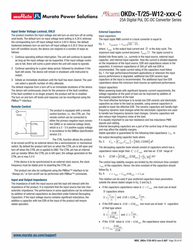
Remote Control
The product is equipped with a remote control function, i.e., the CTRL pin. The remote control can be connected to either the primary negative input connec-tion (GND) or an external voltage (Vext), which is a 3 - 5 V positive supply voltage in accordance to the SMBus Specifi cation version 2.0.
The CTRL function allows the product to be turned on/off by an external device like a semiconductor or mechanical switch. By default the product will turn on when the CTRL pin is left open and turn off when the CTRL pin is applied to GND. The CTRL pin has an internal pull-up resistor. When the CTRL pin is left open, the voltage generated on the CTRL pin is max 5.5 V.
If the device is to be synchronized to an external clock source, the clock frequency must be stable prior to asserting the CTRL pin.
The product can also be confi gured using the PMBus™ interface to be “Always on,” or turn on/off can be performed with PMBus™ commands.
Input and Output Impedance
The impedance of both the input source and the load will interact with the impedance of the product. It is important that the input source has low char-acteristic impedance. The performance in some applications can be enhanced by addition of external capacitance as described under External Decoupling Capacitors. If the input voltage source contains signifi cant inductance, the addition a capacitor with low ESR at the input of the product will ensure stable operation.
CTRL
GND
Vext
External Capacitors
Input capacitors:The input ripple RMS current in a buck converter is equal to
Eq. 1. DDII loadinputRMS 1 ,
where loadI is the output load current and D is the duty cycle. Themaximum load ripple current becomes 2loadI . The ripple current is
divided into three parts, i.e., currents in the input source, external input capacitor, and internal input capacitor. How the current is divided depends on the impedance of the input source, ESR and capacitance values in the capacitors. A minimum capacitance of 300 μF with low ESR is recommended. The ripple current rating of the capacitors must follow Eq. 1. For high-performance/transient applications or wherever the input source performance is degraded, additional low ESR ceramic type capacitors at the input is recommended. The additional input low ESR capacitance above the minimum level insures an optimized performance.
Output capacitors: When powering loads with significant dynamic current requirements, the voltage regulation at the point of load can be improved by addition of decoupling capacitors at the load. The most effective technique is to locate low ESR ceramic and electrolytic capacitors as close to the load as possible, using several capacitors in parallel to lower the effective ESR. The ceramic capacitors will handle high-frequency dynamic load changes while the electrolytic capacitors are used to handle low frequency dynamic load changes. Ceramic capacitors will also reduce high frequency noise at the load. It is equally important to use low resistance and low inductance PWB layouts and cabling. External decoupling capacitors are a part of the control loop of the product and may affect the stability margins. Stable operation is guaranteed for the following total capacitance OC in
the output decoupling capacitor bank where
Eq. 2. 01500 ,300, maxmin CCCO μF.
The decoupling capacitor bank should consist of capacitors which has a capacitance value larger than minCC and has an ESR range of
Eq. 3. 30 ,5 , maxmin ESRESRESR mΩ
The control loop stability margins are limited by the minimum time constant
min of the capacitors. Hence, the time constant of the capacitors should
follow Eq. 4. Eq. 4. s 5.1minminmin ESRC
This relation can be used if your preferred capacitors have parameters outside the above stated ranges in Eq. 2 and Eq.3.
If the capacitors capacitance value is minCC one must use at least
N capacitors where
CCN min and
CCESRESR min
min .
If the ESR value is maxESRESR one must use at least N capacitors
of that type where
ESRmax
ESRN and N
C Cmin .
ESR
If the ESR value is ESR ESRmin the capacitance value should be
C CminESRmin .
OKDx-T/25-W12-xxx-C 25A Digital PoL DC-DC Converter Series
MDC_OKDx-T/25-W12-xxx-C.A07 Page 20 of 41
www.murata-ps.com/support

For a total capacitance outside the above stated range or capacitors that do not follow the stated above requirements above a re-design of the control loop parameters will be necessary for robust dynamic operation and stability.
Control Loop
The product uses a voltage-mode synchronous buck controller with a fi xed frequency PWM scheme. Although the product uses a digital control loop, it operates much like a traditional analog PWM controller. As in the analog controller case, the control loop compares the output voltage to the desired voltage reference and compensation is added to keep the loop stable and fast. The resulting error signal is used to drive the PWM logic. Instead of using external resistors and capacitors required with traditional analog control loops, the product uses a digital Proportional-Integral-Derivative (PID) compensator in the control loop. The characteristics of the control loop is confi gured by setting PID compensation parameters. These PID settings can be reconfi gured using the PMBus™ interface.
Control Loop Compensation Setting
The products without DLC are by default confi gured with a robust control loop compensation setting (PID setting) which allows for a wide range operation of input and output voltages and capacitive loads as defi ned in the section External Decoupling Capacitors. For an application with a specifi c input volt-age, output voltage, and capacitive load, the control loop can be optimized for a robust and stable operation and with an improved load transient response. This optimization will minimize the amount of required output decoupling capacitors for a given load transient requirement yielding an optimized cost and minimized board space. The optimization together with load step simula-tions can be made using the Murata Power Designer software.
Dynamic Loop Compensation (DLC)
Only some of the products that this specifi cation covers have this feature (see section Ordering Information).The DLC feature might in some documents be referred to as “Auto Compen-sation” or “Auto Tuning” feature.
The DLC feature measures the characteristics of the power train and calcu-lates the proper compensator PID coeffi cients.
The default confi guration is that once the output voltage ramp up has completed, the DLC algorithm will begin and a new optimized compensator solution (PID setting) will be found and implemented. The DLC algorithm typi-cally takes between 50 ms and 200 ms to complete.
By the PMBus™ command AUTO_COMP_CONFIG the user may select between several different modes of operation:
Disable
Autocomp once, will run DLC algorithm each time the output is enabled(default confi guration)
Autocomp every second will initiate a new DLC algorithm each 1 second
Autocomp every minute will initiate a new DLC algorithm every minute.The DLC can also be confi gured to run once only after the fi rst ramp up (afterinput power have been applied) and to use that temporary stored PID settingsin all subsequent ramps. If input power is cycled a new DLC algorithm will be performed after the fi rst ramp up. The default setting is however to run the DLCalgorithm after every ramp up.
The DLC algorithm can also be initiated manually by sending the AUTO_COMP_CONTROL command.
The DLC can also be confi gured with Auto Comp Gain Control. This scales the DLC results to allow a trade-off between transient response and steady-state duty cycle jitter. A setting of 100% will provide the fastest transient response while a setting of 10% will produce the lowest jitter. The default is 50%.
Changing DLC and PID Setting
Some caution must be considered while DLC is enabled and when it is changed from enabled or disabled.
When operating, the controller IC uses the settings loaded in its (volatile) RAM memory. When the input power is applied the RAM settings are retrieved from the pin-strap resistors and the two non-volatile memories (DEFAULT and USER). The sequence is described in the “Initialization Procedure” section.
When DLC is enabled:When DLC is enabled, the normal sequence (after input power has been applied) that a value stored in the user non-volatile memory overwrites any previously loaded value does not apply for the PID setting (stored in the PID_TAPS register). The PID setting in the user non-volatile memory is ignored and a non-confi gurable default PID setting is loaded to RAM to act as a safe starting value for the DLC. Once the output has been enabled and the DLC algorithm has found a new optimized PID setting it will be loaded in RAM and used by the control loop.
When saving changes to the user non-volatile memory, all changes made to the content of RAM will be saved. This also includes the default PID setting (loaded to RAM to act as a safe starting value) or the PID setting changed by the DLC algorithm after enabling output. The result is that as long as DLC is enabled the PID setting in the user non-volatile memory is ignored, but it might accidentally get overwritten.
When changing DLC from disabled to enabled:A non-confi gurable default PID setting is loaded to RAM to act as a safe start-ing value for the DLC (same as above).
When changing DLC from enabled to disabled:When changing DLC from enabled to disabled, the PID setting in the user non-volatile memory will be loaded to RAM. Any new optimized PID setting in RAM will be lost, if not fi rst stored to the user non-volatile memory.
When DLC is disabled:When DLC is disabled and input power has been applied, the PID setting in the user non-volatile memory will be loaded to RAM and used in the control loop.The original PID setting in the user non-volatile memory is quite slow and not recommended for optimal performance. If DLC is disabled it is recommended to either:
1. Use the DLC to fi nd optimized PID setting.
2. Use Murata Power Designer to fi nd appropriate PID setting.
3. Use Universal PID as defi ned below.
OKDx-T/25-W12-xxx-C 25A Digital PoL DC-DC Converter Series
MDC_OKDx-T/25-W12-xxx-C.A07 Page 21 of 41
www.murata-ps.com/support

The output voltage and the maximum output voltage can be pin strapped to three fi xed values by connecting the VSET pin according to the table below.
Output Voltage Adjust using PMBus™
The output voltage set by pin-strap can be overridden by confi guration fi le or by using a PMBus™ command. See Electrical Specifi cation for adjustment range.
When setting the output voltage by confi guration fi le or by a PMBus™ command, the specifi ed output voltage accuracy is valid only when the set output voltage level falls within the same bin range as the voltage level defi ned by the pin-strap resistor RSET. The applicable bin ranges are defi ned in the table below. Valid accuracy for voltage levels outside the applicable bin range is two times the specifi ed.
Example:Nominal VO is set to 1.10 V by RSET = 26.1 kΩ. 1.10 V falls within the bin range 0.988-1.383 V, thus specifi ed accuracy is valid when adjusting VO within 0.988-1.383V.
Output Voltage Range Limitation
The output voltage range that is possible to set by confi guration or by the PMBus™ interface is limited by the pin-strap resistor RSET. The maximum output voltage is set to 110% of the nominal output value defi ned by RSET, VO,MAX = 1.1 x VO,RSET. This protects the load from an over voltage due to an accidental wrong PMBus™ command.
The Universal PID setting (taps) is:
A = 4580.75,
B = -8544.00,
C = 3972.81
Write 0x7CF84DFE85807D8F26 to PID_TAPS register and write com-mand STORE_USER_ALL
Note that if DLC is enabled, for best results VI must be stable before DLC algorithm begins.
Load Transient Response Optimization
The product incorporates a Non-Linear transient Response, NLR, loop that decreases the response time and the output voltage deviation during a load transient. The NLR results in a higher equivalent loop bandwidth than is pos-sible using a traditional linear control loop. The product is pre-confi gured with appropriate NLR settings for robust and stable operation for a wide range of input voltage and a capacitive load range as defi ned in the section External Decoupling Capacitors. For an application with a specifi c input voltage, output voltage, and capacitive load, the NLR confi guration can be optimized for a robust and stable operation and with an improved load transient response. This will also reduce the amount of output decoupling capacitors and yield a reduced cost. However, the NLR slightly reduces the effi ciency. In order to obtain maximal energy effi ciency the load transient requirement has to be met by the standard control loop compensation and the decoupling capacitors. The NLR settings can be reconfi gured using the PMBus™ interface.
Remote Sense
The product has remote sense that can be used to compensate for voltage drops between the output and the point of load. The sense traces should be located close to the PWB ground layer to reduce noise susceptibility. Due to derating of internal output capacitance the voltage drop should be kept below VDROPMAX = (5.25 – VOUT) / 2. A large voltage drop will impact the electrical performance of the regulator. If the remote sense is not needed, +S should be connected to VOUT and −S should be connected to GND.
Output Voltage Adjust using Pin-strap Resistor
Using an external Pin-strap resistor, RSET, the output voltage can be set in the range 0.6 V to 3.3 V at 28 different levels shown in the table below. The resistor should be applied between the VSET pin and the PREF pin.
RSET also sets the maximum output voltage, see section “Output Voltage Range Limitation.” The resis-
tor is sensed only during product start-up. Changing the resistor value during normal operation will not change the output voltage. The input voltage must be at least 1 V larger than the output voltage in order to deliver the correct output voltage. See Ordering Information for output voltage range.
The following table shows recommended resistor values for RSET. Maxi-mum 1% tolerance resistors are required.
VO bin ranges [V]
0.600 – 0.9880.988 – 1.3831.383 – 1.9751.975 – 2.3982.398 – 2.9632.963 – 3.753
VSET
R SET
PREF
VO [V] RSET[kΩ] VO [V] RSET[kΩ]
0.60 10 1.50 46.40.65 11 1.60 51.10.70 12.1 1.70 56.20.75 13.3 1.80 61.90.80 14.7 1.90 68.10.85 16.2 2.00 750.90 17.8 2.10 82.50.95 19.6 2.20 90.91.00 21.5 2.30 1001.05 23.7 2.50 1101.10 26.1 3.00 1211.15 28.7 3.30 1331.20 31.61.25 34.81.30 38.31.40 42.2
VO [V] VSET
0.60 Shorted to PREF1.2 Open “high impedance”2.5 Logic High, GND as reference
OKDx-T/25-W12-xxx-C 25A Digital PoL DC-DC Converter Series
MDC_OKDx-T/25-W12-xxx-C.A07 Page 22 of 41
www.murata-ps.com/support

Switching Frequency
The fundamental switching frequency is 320 kHz, which yields optimal power effi ciency. The switching frequency can be set to any value between 200 kHz and 640 kHz using the PMBus™ interface. The switching frequency will change the effi ciency/power dissipation, load transient response and output ripple. For optimal control loop performance in a product without DLC, the control loop must be re-optimized when changing the switching frequency.
Synchronization
Synchronization is a feature that allows multiple products to be synchronized to a common frequency. Synchronized products powered from the same bus eliminate beat frequencies refl ected back to the input supply, and also reduces EMI fi ltering requirements. Eliminating the slow beat frequencies (usually <10 kHz) allows the EMI fi lter to be designed to attenuate only the synchronization frequency. Synchronization can also be utilized for phase spreading, described in section Phase Spreading.
The products can be synchronized with an external oscillator or one product can be confi gured with the SYNC pin as a SYNC Output working as a master driving the synchronization. All others on the same synchronization bus must be confi gured with SYNC Input. Default confi guration is using the internal clock, independently of signal at the SYNC pin.
Phase Spreading
When multiple products share a common DC input supply, spreading of the switching clock phase between the products can be utilized. This dramatically reduces input capacitance requirements and effi ciency losses, since the peak current drawn from the input supply is effectively spread out over the whole switch period. This requires that the products are synchronized. Up to 16 dif-ferent phases can be used.
The phase spreading of the product can be confi gured using the PMBus™ interface.
Parallel Operation (Current Sharing)
Paralleling multiple products can be used to increase the output current capability of a single power rail. By connecting the GCB pins of each device and confi guring the devices as a current sharing rail, the units will share the current equally, enabling up to 100% utilization of the current capability for each device in the current sharing rail. The product uses a low-bandwidth, fi rst-order digital current sharing by aligning the output voltage of the slave devices to deliver the same current as the master device. Artifi cial droop resistance is added to the output voltage path to control the slope of the load line curve, calibrating out the physical parasitic mismatches due to power train components and PWB layout. Up to 7 devices can be confi gured in a given current sharing group.
In order to avoid interference with other algorithms executing during parallel operation, the dead-time algorithm should be turned off and fi xed dead-times be used.
Phase Adding and Shedding for Parallel Operation
During periods of light loading, it may be benefi cial to disable one or more phases (modules) in order to eliminate the current drain and switching losses associated with those phases, resulting in higher effi ciency. The product offers the ability to add and drop phases (modules) using a PMBus™ command in response to an observed load current change. All phases (modules) in a current share rail are considered active prior to the current sharing rail ramp to power-good. Phases can be dropped after power-good is reached. Any member of the current sharing rail can be dropped. If the reference module is
Output Voltage Adjust Limitation using PMBus™
In addition to the maximum output voltage limitation by the pin-strap resis-tor RSET, there is also a limitation in how much the output voltage can be increased while the output is enabled. If output is disabled then RSET resistor is the only limitation.
Example: If the output is enabled with output voltage set to 1.0 V, then it is only possible to adjust/change the output voltage up to 1.7- V as long as the output is enabled.
Over Voltage Protection (OVP)
The product includes over voltage limiting circuitry for protection of the load. The default OVP limit is 15% above the nominal output voltage. If the output voltage exceeds the OVP limit, the product can respond in different ways:
1. Initiate an immediate shutdown until the fault has been cleared. The usercan select a specifi c number of retry attempts.
2. Turn off the high-side MOSFET and turn on the low-side MOSFET. Thelow-side MOSFET remains ON until the device attempts a restart, i.e. theoutput voltage is pulled to ground level (crowbar function).
The default response from an overvoltage fault is to immediately shut down as in 2. The device will continuously check for the presence of the fault condition, and when the fault condition no longer exists the device will be re-enabled. For continuous OVP when operating from an external clock for syn-chronization, the only allowed response is an immediate shutdown. The OVP limit and fault response can be reconfi gured using the PMBus™ interface.
Under Voltage Protection (UVP)
The product includes output under voltage limiting circuitry for protection of the load. The default UVP limit is 15% below the nominal output voltage. The UVP limit can be reconfi gured using the PMBus™ interface.
Power Good
The product provides a Power Good (PG) fl ag in the Status Word register that indicates the output voltage is within a specifi ed tolerance of its target level and no fault condition exists. If specifi ed in section Connections, the product also provides a PG signal output. The PG pin is active high and by default open-drain but may also be confi gured as push-pull via the PMBus™ interface.
By default, the PG signal will be asserted when the output reaches above 90% of the nominal voltage, and de-asserted when the output falls below 85% of the nominal voltage. These limits may be changed via the PMBus™ interface. A PG delay period is defi ned as the time from when all conditions within the product for asserting PG are met to when the PG signal is actually asserted. The default PG delay is set to 10 ms. This value can be reconfi gured using the PMBus™ interface.
For products with DLC the PG signal is by default asserted directly after the DLC operation have been completed. If DLC is disabled the confi gured PG delay will be used. This can be reconfi gured using the PMBus™ interface.
VO setting
when enabled [V]
VO set range
while enabled [V]
0.000 – 0.988 ~0.2 to >1.20.988 – 1.383 ~0.2 to >1.71.383 – 1.975 ~0.2 to >2.51.975 – 2.398 ~0.2 to >2.972.398 – 2.963 ~0.2 to >3.682.963 – 3.753 ~0.2 to >4.65
OKDx-T/25-W12-xxx-C 25A Digital PoL DC-DC Converter Series
MDC_OKDx-T/25-W12-xxx-C.A07 Page 23 of 41
www.murata-ps.com/support

The default settings for the soft-start delay period and the soft-start ramp time is 10 ms. Hence, power-up is completed within 20 ms in default con-fi guration using remote control. When the soft-start delay time is set to 0 ms, the module will begin its ramp-up after the internal circuitry has initialized (approximately 2 ms). It is generally recommended to set the soft-start ramp-up time to a value greater than 500 μs to prevent inadvertent fault condi-tions due to excessive inrush current. The acctual minimum ramp-up time will however normally be limited by the control loop settings and ramp-up times of internal interface voltages in the controller circuit to approximately 2 ms. The soft-start power up of the product can be reconfi gured using the PMBus™ interface.
Output Voltage Sequencing
A group of products may be confi gured to power up in a predetermined sequence. This feature is especially useful when powering advanced proces-sors, FPGAs, and ASICs that require one supply to reach its operating voltage prior to another. Multi-product sequencing can be achieved by confi guring the start delay and rise time of each device through the PMBus™ interface and by using the CTRL start signal.
Voltage Tracking
The product integrates a lossless tracking scheme that allows its output to track a voltage that is applied to the VTRK pin with no external components required. During ramp-up, the output voltage follows the VTRK voltage until the preset output voltage level is met. The product offers two modes of track-ing as follows:
1. Coincident. This mode confi gures the product to ramp its output voltage atthe same rate as the voltage applied to the VTRK pin.
2. Ratiometric. This mode confi gures the product to ramp its output voltageat a rate that is a percentage of the voltage applied to the VTRK pin. Thedefault setting is 50%, but a different tracking ratio may be set by anexternal resistive voltage divider or through the PMBus™ interface.
dropped, the remaining active module with the lowest member position will become the new reference. Additionally, any change to the number of mem-bers of a current sharing rail will precipitate autonomous phase distribution within the rail where all active phases realign their phase position based on their order within the number of active members. If the members of a current sharing rail are forced to shut down due to an observed fault, all members of the rail will attempt to re-start simultaneously after the fault has cleared.
Effi ciency Optimized Dead Time Control
The product utilizes a closed loop algorithm to optimize the dead-time applied between the gate drive signals for the switch and synch FETs. The algorithm constantly adjusts the deadtime non-overlap to minimize the duty cycle, thus maximizing effi ciency. This algorithm will null out deadtime differences due to component variation, temperature and loading effects. The algorithm can be confi gured via the PMBus™ interface.
Over Current Protection (OCP)
The product includes current limiting circuitry for protection at continuous overload. The following OCP response options are available:
1. Initiate a shutdown and attempt to restart an infi nite number of times witha preset delay period between attempts.
2. Initiate a shutdown and attempt to restart a preset number of times with apreset delay period between attempts.
3. Continue operating for a given delay period, followed by shutdown if thefault still exists.
4. Continue operating through the fault (this could result in permanentdamage to the power supply).
5. Initiate an immediate shutdown.
The default response from an over current fault is an immediate shutdownof the device. The device will continuously check for the presence of the fault condition, and if the fault condition no longer exists the device will be re-enabled. The load distribution should be designed for the maximum output short circuit current specifi ed. The OCP limit and response of the product can be reconfi gured using the PMBus™ interface.
Initialization Procedure
The product follows a specifi c internal initialization procedure after power is applied to the VIN pin:
1. Status of the address and output voltage pin-strap pins are checked and values associated with the pin settings are loaded to RAM.
2. Values stored in the Murata default non-volatile memory are loaded toRAM. This overwrites any previously loaded values.
3. Values stored in the user non-volatile memory are loaded to RAM. Thisoverwrites any previously loaded values.
Once the initialization process is completed, the product is ready to beenabled using the CTRL pin. The product is also ready to accept commands via the PMBus™ interface, which will overwrite any values loaded during the initialization procedure.
Soft-start Power Up
The soft-start control introduces a time-delay before allowing the output voltage to rise. Once the initialization time has passed the device will wait for the confi gured delay period prior to starting to ramp its output. After the delay period has expired, the output will begin to ramp towards its target voltage according to the confi gured soft-start ramp time.
VIN
CTRL
VOUT
timeDelay Initialization time
Ramp time
Illustration of Power Up Procedure
Illustration of Output Voltage Sequencing.
t
V1
V2
VOUT
OKDx-T/25-W12-xxx-C 25A Digital PoL DC-DC Converter Series
MDC_OKDx-T/25-W12-xxx-C.A07 Page 24 of 41
www.murata-ps.com/support

where RGCB is the pull up resistor value and CGCB is the bus loading. The pull-up resistor should be tied to an external supply voltage in range from 3.3 to 5 V, which should be present priorμ to or during power-up.
If exploring untested compensation or deadtime confi gurations, it is recom-mended that 27 Ω series resistors are placed between the GCB pin of each product and the common GCB connection. This will avoid propagation of faults between products potentially caused by hazardous confi guration settings. When the confi gurations of the products are settled the series resistors can be removed.
The GCB is an internal bus, such that it is only connected across the mod-ules and not the PMBus™ system host. GCB addresses are assigned on a rail level, i.e. modules within the same current sharing group share the same GCB address. Addressing rails across the GCB is done with a 5 bit GCB ID, yielding a theoretical total of 32 rails that can be shared with a single GCB bus.
Fault Spreading
The product can be confi gured to broadcast a fault event over the GCB bus to the other devices in the group. When a non-destructive fault occurs and the device is confi gured to shut down on a fault, the device will shut down and broadcast the fault event over the GCB bus. The other devices on the GCB bus will shut down together if confi gured to do so, and will attempt to re-start in their prescribed order if confi gured to do so.
Over Temperature Protection (OTP)
The products are protected from thermal overload by an internal over tempera-ture shutdown function in the controller circuit N1, located at position P2 (see section Thermal Consideration). Some of the products that this specifi cation covers use the temperature at position P2 (TP2) as a reference for specifi ed OTP threshold and some use position P1 (TP1) as a reference for specifi ed OTP threshold. See the Over Temperature Protection section in the electrical specifi -cation for each product.
Products with P1 as reference for OTP:When TP1 as defi ned in thermal consideration section exceeds approxi-mately 120 °C the product will shut down. The specifi ed OTP threshold and hysteresis are valid for worst case operation regarding cooling conditions, input voltage and output voltage. The actually confi gured default value in the controller circuit in position P2 is 110 °C, but at worst case operation the temperature is approximately 10 °C higher at position P1. At light load the temperature is approximately the same in position P1 and P2. This means the OTP threshold and hysteresis will be lower at light load conditions when P1 is used as a reference for OTP.
Products with P2 as reference OTP:When TP2 as defi ned in thermal consideration section exceeds 120°C the product will shut down. For products with P2 as a reference for OTP the con-fi gured default value in the controller circuit in position P2 is 120°C.
The OTP threshold, hysteresis, and fault response of the product can be reconfi gured using the PMBus™ interface. The fault response can be confi g-ured as follows:
1. Initiate a shutdown and attempt to restart an infi nite number of times witha preset delay period between attempts (default confi guration).
2. Initiate a shutdown and attempt to restart a preset number of times with apreset delay period between attempts.
3. Continue operating for a given delay period, followed by shutdown if thefault still exists.
The master device in a tracking group is defi ned as the device that has the highest target output voltage within the group. This master device will control the ramp rate of all tracking devices and is not confi gured for tracking mode. All of the CTRL pins in the tracking group must be connected and driven by a single logic source. It should be noted that current sharing groups that are also confi gured to track another voltage do not offer pre-bias protection; a minimum load should therefore be enforced to avoid the output voltage from being held up by an outside force.
Voltage Margining Up/Down
The product can adjust its output higher or lower than its nominal voltage setting in order to determine whether the load device is capable of operating over its specifi ed supply voltage range. This provides a convenient method for dynamically testing the operation of the load circuit over its supply margin or range. It can also be used to verify the function of supply voltage supervisors. Margin limits of the nominal output voltage ±5% are default, but the margin limits can be reconfi gured using the PMBus™ interface.
Pre-Bias Startup Capability
Pre-bias startup often occurs in complex digital systems when current from another power source is fed back through a dual-supply logic component, such as FPGAs or ASICs. The product family incorporates synchronous recti-fi ers, but will not sink current during startup, or turn off, or whenever a fault shuts down the product in a pre-bias condition. Pre-bias protection is not offered for current sharing groups that also have voltage tracking enabled.
Group Communication Bus
The Group Communication Bus, GCB, is used to communicate between products. This dedicated bus provides the communication channel between devices for features such as sequencing, fault spreading, and current sharing. The GCB solves the PMBus™ data rate limitation. The GCB pin on all devices in an application should be connected together. A pull-up resistor is required on the common GCB in order to guarantee the rise time as follows:
Eq. 5. = RGCB CGCB ≤ 1μs,
Illustration of Ratiometric Voltage Tracking
t
MASTER
SLAVE
VOUT
Illustration of Coincident Voltage Tracking.
t
MASTER
SLAVE
VOUT
OKDx-T/25-W12-xxx-C 25A Digital PoL DC-DC Converter Series
MDC_OKDx-T/25-W12-xxx-C.A07 Page 25 of 41
www.murata-ps.com/support

4. Continue operating through the fault (this could result in permanentdamage to the power supply).
5. Initiate an immediate shutdown.
Optimization examples
This product is designed with a digital control circuit. The control circuit uses a confi guration fi le which determines the functionality and performance of the product. It is possible to change the confi guration fi le to optimize certain performance characteristics. In the table below is a schematic view on how to change different confi guration parameters in order to achieve an optimization towards a wanted performance.
Increase No change Decrease
Config.
parameters
Switching
frequency
Control
loop
bandwidth
NLR
threshold
Diode
emulation
(DCM)
Min.
pulse
Optimized performanceMaximizeeffi ciency Enable Disable
Minimizeripple ampl.
Enableor
disable
Enable or disable
Improve load transient response Disable Disable
Minimizeidle power loss Enable Enable
Note 1: The following table, graphs and waveforms are only examples and valid for OKDY-T/25-W12-001-C and OKDH-T/25-W12-001-C.Note 2: In the following table and graphs, the worst-case scenario (load step 18.75-6.25 A) has been considered for load transient.
Pli
Input idling power (no load)
Default confi guration: Continues Conduction Mode, CCM
VO = 0.6 V 0.56
WVO = 1.0 V 0.57VO = 1.8 V 0.67VO = 3.3 V 0.92
DCM, Discontinues Conduction Mode(diode emulation)
VO = 0.6 V 0.20
WVO = 1.0 V 0.20VO = 1.8 V 0.20VO = 3.3 V 0.20
DCM with Minimum Pulse Enabled
VO = 0.6 V 0.32
WVO = 1.0 V 0.33VO = 1.8 V 0.35VO = 3.3 V 0.43
PCTRLInput standby power
Turned off with CTRL-pin
Default confi guration:Monitoring enabled
170 mW
Pulse monitor mode:Monitoring disabled
108 mW
Low power mode:Monitoring disabled
84 mW
Vtr1
Load transient peak voltage deviation
Load step 25-75-25% of max IO
Default confi guration di/dt = 2 A/μsCO = 470 μF
VO = 0.6 V 95
mVVO = 1.0 V 105VO = 1.8 V 115VO = 3.3 V 168
DLC and Optimized NLR confi gurationdi/dt = 2 A/μsCO = 470 μF
VO = 0.6 V 63
mVVO = 1.0 V 71VO = 1.8 V 79VO = 3.3 V 108
ttr1
Load transient recovery time
Load step 25-75-25% of max IO
Default confi guration di/dt = 2 A/μsCO=470 μF
VO = 0.6 V 74
μs
VO = 1.0 V 85VO = 1.8 V 122VO = 3.3 V 140
DLC and Optimized NLR confi gurationdi/dt = 2 A/μsCO = 470 μF
VO = 0.6 V 40VO = 1.0 V 40VO = 1.8 V 50VO = 3.3 V 50
Efficiency vs. Output Current and Switching frequency
Efficiency vs. load current and switching frequency at TP1 = +25 °C, VI = 12 V, VO = 1.0 V, CO = 470 μF/10 m Default configuration except changed frequency
Load transient vs. Switching frequency
Load transient peak voltage deviation vs. frequency. Step-change (6.25-18.75-6.25 A). TP1 = +25 °C, VI = 12 V, VO =1.0 V, CO = 470 μF/10 m
70
75
80
85
90
95
0 5 10 15 20 25
[%]
[A]
200kHz
320kHz
480kHz
640kHz
0
100
200
300
400
200 300 400 500 600
[mV]
[kHz]
Universal PID,No NLR
DLC, NoNLR
Universal PID,Default NLR
DLC,Default NLR
Universal PID,Opt. NLR
DLC,Opt. NLR
OKDx-T/25-W12-xxx-C 25A Digital PoL DC-DC Converter Series
MDC_OKDx-T/25-W12-xxx-C.A07 Page 26 of 41
www.murata-ps.com/support

Power Dissipation vs. Output Current and Switching frequency
Output Ripple vs. Switching frequency
Dissipated power vs. load current and switching frequency at TP1 = +25 °C, VI = 12 V, VO = 1.0 V, CO = 470 μF/10 m Default configuration except changed frequency
Output voltage ripple Vpk-pk at: TP1 = +25 °C, VI = 12 V, CO = 470 μF/10 m , IO = 25 A resistive load. Default configuration except changed frequency.
Load Transient vs. Decoupling Capacitance, VO = 1.0 V
Load Transient vs. Decoupling Capacitance, VO = 3.3 V
Load transient peak voltage deviation vs. decoupling capacitance. Step (6.25-18.75-6.25 A). Parallel coupling of capacitors with 470 μF/10 m , TP1 = +25 °C. VI = 12 V, VO = 1.0 V, fsw = 320 kHz, di/dt = 2 A/μs
Load transient peak voltage deviation vs. decoupling capacitance. Step (6.25-18.75-6.25 A). Parallel coupling of capacitors with 470 μF/10 m , TP1 = +25 °C. VI = 12 V, VO = 3.3 V, fsw = 320 kHz, di/dt = 2 A/μs
0
1
2
3
4
5
6
0 5 10 15 20 25 [A]
[W]
200kHz
320kHz
480kHz
640kHz
0
30
60
90
120
150
200 300 400 500 600
[mVpk-pk]
[kHz]
0.6 V
1.0 V
1.8 V
3.3 V
0
100
200
300
400
210 53 4
[mV]
[mF]
Universal PID,No NLR
DLC, NoNLR
Universal PID,Default NLR
DLC,Default NLR
Universal PID,Opt. NLR
DLC, Opt.NLR
0
100
200
300
400
20 1 3 54
[mV]
[mF]
Universal PID,No NLRDLC, NoNLRUniversal PID,Default NLR
DLC,Default NLRUniversal PID,Opt. NLRDLC, Opt.NLR
OKDx-T/25-W12-xxx-C 25A Digital PoL DC-DC Converter Series
MDC_OKDx-T/25-W12-xxx-C.A07 Page 27 of 41
www.murata-ps.com/support

Output Load Transient Response, Default Configuration
Output Load Transient Response, DLC and No NLR
Output voltage response to load current step-change (6.25-18.75-6.25 A) at: TP1 = +25 °C, VI = 12 V, VO = 1.0 V di/dt=2 A/μs, fsw = 320 kHz, CO = 470 μF/10 m Default configuration (DLC and default NLR)
Top trace: output voltage (200 mV/div.). Bottom trace: load current (5 A/div.). Time scale: (0.1 ms/div.).
Output voltage response to load current step-change (6.25-18.75-6.25 A) at: TP1 = +25 °C, VI = 12 V, VO = 1.0 V di/dt=2 A/μs, fsw = 320 kHz, CO = 470 μF/10 m DLC and no NLR
Output Load Transient Response, DLC and Optimized NLR
Top trace: output voltage (200 mV/div.). Bottom trace: load current (5 A/div.). Time scale: (0.1 ms/div.).
Output voltage response to load current step-change (6.25-18.75-6.25 A) at: TP1 = +25 °C, VI = 12 V, VO = 1.0 V di/dt=2 A/μs, fsw = 320 kHz, CO = 470 μF/10 m DLC and optimized NLR
Top trace: output voltage (200 mV/div.). Bottom trace: load current (5 A/div.). Time scale: (0.1 ms/div.).
OKDx-T/25-W12-xxx-C 25A Digital PoL DC-DC Converter Series
MDC_OKDx-T/25-W12-xxx-C.A07 Page 28 of 41
www.murata-ps.com/support

Defi nition of reference temperature TP1The reference temperature is used to monitor the temperature limits of the product. Temperature above maximum TP1, measured at the reference point P1 is not allowed and may cause degradation or permanent damage to the product. TP1 is also used to defi ne the temperature range for normal operat-ing conditions. TP1 is defi ned by the design and used to guarantee safety margins, proper operation and high reliability of the product.
Thermal Consideration
GeneralThe product is designed to operate in different thermal environments and suf-fi cient cooling must be provided to ensure reliable operation.
Cooling is achieved mainly by conduction, from the pins to the host board, and convection, which is dependent on the airfl ow across the product. Increased airfl ow enhances the cooling of the product.
The Output Current Derating graph found in the Output section for each model provides the available output current vs. ambient air temperature and air velocity at specifi ed VI.
The product is tested on a 254 x 254 mm, 35 μm (1 oz), test board mounted vertically in a wind tunnel with a cross-section of 608 x 203 mm. The test board has 8 layers.
Proper cooling of the product can be verifi ed by measuring the temperature at positions P1 and P2. The temperature at these positions should not exceed the max values provided in the table below.
Note that the max value is the absolute maximum rating (non destruction) and that the electrical Output data is guaranteed up to TP1 +95°C.
Defi nition of product operating temperatureThe product operating temperatures are used to monitor the temperature of the product, and proper thermal conditions can be verifi ed by measuring the temperature at positions P1 and P2. The temperature at these positions (TP1, TP2) should not exceed the maximum temperatures in the table below. The number of measurement points may vary with different thermal design and topology. Temperatures above maximum TP1, measured at the reference point P1 are not allowed and may cause permanent damage. It should also be noted that depending on setting of the over temperature protection (OTP) and operating conditions, the product may shut down before the maximum allowed temperature at TP1 is reached.Position Description Max Temp.
P1 Reference point, L1, inductor 125°C*
P2 N1, control circuit 125°C*
* A guard band of 5 °C is applied to the maximum recorded component temperatures when calculating output current derating curves.
P1
AIR FLOW
P2
SIP Version:Temperature positions and air fl ow direction.
P2
AIR FLOW
P1
Top view Bottom view
Temperature positions and air fl ow direction.
OKDx-T/25-W12-xxx-C 25A Digital PoL DC-DC Converter Series
MDC_OKDx-T/25-W12-xxx-C.A07 Page 29 of 41
www.murata-ps.com/support

Pin Designation Function
1A VIN Input Voltage2A GND Power Ground3A VOUT Output Voltage4A +S Positive sense4B −S Negative sense5A VSET Output voltage pin-strap5B VTRK Voltage Tracking input6A SALERT PMBus Alert6B SDA PMBus Data7A SCL PMBus Clock7B SA1 PMBus address pin-strap 18A SA0 PMBus address pin-strap 08B SYNC Synchronization I/O9A PG Power Good9B CTRL Remote Control10A GCB Group Communication Bus10B PREF Pin-strap reference
Pin Designation Function
1A VIN Input Voltage2A GND Power Ground3A VOUT Output Voltage4A VTRK or PG* Voltage Tracking input or Power Good4B PREF Pin-strap reference5A +S Positive sense5B −S Negative sense6A SA0 PMBus address pin-strap6B GCB Group Communication Bus7A SCL PMBus Clock7B SDA PMBus Data8A VSET Output voltage pin-strap8B SYNC Synchronization I/O9A SALERT PMBus Alert9B CTRL Remote Control
* OKDH-T/25-W12-001-C, OKDY-T/25-W12-001-C, OKDH-T/25-W12-001-C, OKDY-T/25-W12-001-C:Pin 4A = VTRK pin.
OKDH-T/25-W12G-001-C, OKDY-T/25-W12G-001-C, OKDH-T/25-W12G-001-C, OKDY-T/25-W12G-001-C:Pin 4A = PG pin.For these products the PG pin is internally tied to the VTRK input of the products’ controller. Typically the VTRK input bias current will be equivalent to a 50 kΩ pull-down resistor. This should be considered when choosing pull-up resistor for the PG signal.
SIP Version: Pin layout, top view (component placement for illustration only).Pin layout, top view (component placement for illustration only).
OKDx-T/25-W12-xxx-C 25A Digital PoL DC-DC Converter Series
MDC_OKDx-T/25-W12-xxx-C.A07 Page 30 of 41
www.murata-ps.com/support

Typical Application Circuit
Standalone operation with PMBus™ communication. Top view of product footprint.
Unused input pinsUnused SDA, SCL and GCB pins should still have pull-up resistors as specifi ed.
Unused VTRK or SYNC pins should be left open or connected to the PREF pin.
Unused CTRL pin can be left open due to internal pull-up.
VSET and SA0/SA1 pins must be used. These pins must have pin-strap resistors or strapping settings as specifi ed.
PWB layout considerationsThe pin-strap resistors, RSET, and RSA0/RSA1 should be placed as close to the product as possible to minimize loops that may pick up noise.
Avoid current carrying planes under the pin-strap resistors and the PMBus™ signals.
The capacitor CI (or capacitors implementing it) should be placed as close to the input pins as possible.
Capacitor CO (or capacitors implementing it) should be placed close to the load.
Care should be taken in the routing of the connections from the sensed output voltage to the S+ and S– terminals. These sensing connections should be routed as a differential pair, preferably between ground planes which are not carrying high currents. The routing should avoid areas of high electric or magnetic fi elds.
OKDx-T/25-W12-xxx-C 25A Digital PoL DC-DC Converter Series
MDC_OKDx-T/25-W12-xxx-C.A07 Page 31 of 41
www.murata-ps.com/support

Typical Application Circuit (SIP version)
Typical Application Circuit (Parallel Operation)
Standalone operation with PMBus™ communication. Top view of product footprint.
Parallel operation.
OKDx-T/25-W12-xxx-C 25A Digital PoL DC-DC Converter Series
MDC_OKDx-T/25-W12-xxx-C.A07 Page 32 of 41
www.murata-ps.com/support

fault has occurred. Automatic store to Flash memory following a fault is trig-gered when any fault threshold level is exceeded, provided that the specifi c fault response is to shut down. Writing to Flash memory is not allowed if the device is confi gured to restart following the specifi c fault condition. It should also be noted that the device supply voltage must be maintained during the time the device is writing data to Flash memory; a process that requires between 700-1400 μs depending on whether the data is set up for a block write. Undesirable results may be observed if the input voltage of the product drops below 3.0 V during this process.
Non-Volatile Memory (NVM)
The product incorporates two Non-Volatile Memory areas for storage of the sup-ported PMBus™ commands; the Default NVM and the User NVM.
The Default NVM is pre-loaded with Murata factory default values. The Default NVM is write-protected and can be used to restore the Murata factory default values through the command RESTORE_DEFAULT_ALL.
The User NVM is pre-loaded with Murata factory default values. The User NVM is writable and open for customization. The values in NVM are loaded into operational RAM during initialization according to section “Initialization Procedure”, where after commands can be changed through the PMBus™ Interface. The STORE_USER_ALL command will store the changed param-eters to the User NVM.
Software tools for design and production
Murata provides software tools for confi guration and monitoring of this prod-uct via the PMBus™ interface. For more information please contact your local Murata sales representative.
PMBus™ addressing
The PMBus™ address should be confi gured with resistors connected between the SA0/SA1 pins and the PREF pin, as shown in the fi gure below. Recommended resistor values for hard-wiring PMBus™ addresses are shown in the table. 1% tolerance resistors are required.
PMBus™ interface
This product provides a PMBus™ digital interface that enables the user to confi gure many aspects of the device operation as well as to monitor the input and output voltages, output current and device temperature. The product can be used with any standard two-wire I2C or SMBus host device. In addition, the product is compatible with PMBus™ version 1.1 and includes an SALERT line to help mitigate bandwidth limitations related to continuous fault monitor-ing. The product supports 100 kHz bus clock frequency only. The PMBus™ signals, SCL, SDA and SALERT require passive pull-up resistors as stated in the SMBus Specifi cation. Pull-up resistors are required to guarantee the rise time as follows:
Eq. 6. = Rp Cp ≤ 1μs,
where Rp is the pull-up resistor value and Cp is the bus loading, the maximum allowed bus load is 400 pF. The pull-up resistor should be tied to an external supply voltage in range from 2.7 to 5.5 V, which should be present prior to or during power-up. If the proper power supply is not available, voltage dividers may be applied. Note that in this case, the resistance in the equation above corresponds to parallel connection of the resistors forming the voltage divider.
Monitoring via PMBus™
It is possible to monitor a wide variety of parameters through the PMBus™ interface. Fault conditions can be monitored using the SALERT pin, which will be asserted when any number of pre-confi gured fault or warning conditions occurs. It is also possible to continuously monitor one or more of the power conversion parameters including but not limited to the following:
Input voltage (READ_VIN)
Output voltage (READ_VOUT)
Output current (READ_IOUT)
Internal junction temperature (READ_TEMPERATURE_1)
Switching frequency (READ_FREQUENCY)
Duty cycle (READ_DUTY_CYCLE)
In the default confi guration monitoring is enabled also when the outputvoltage is disabled. This can be changed in order to reduce standby powerconsumption.
Snap shot parameter capture
This product offers a special feature that enables the user to captureparametric data during normal operation or following a fault. The followingparameters are stored:
Input voltage
Output voltage
Output current
Internal junction temperature
Switching frequency
Duty cycle
Status registers
The Snapshot feature enables the user to read the parameters via thePMBus™ interface during normal operation, although it should be noted thatreading the 22 bytes will occupy the bus for some time. The Snapshot enablesthe user to store the snapshot parameters to Flash memory in response to apending fault as well as to read the stored data from Flash memory after a
User NVM Factory default Customizable
RAM
RESTORE_DEFAULT_ALL
Default NVM Factory default Write-protected
READ
WRITE
PMBus interface
STORE_USER_ALL
INITIALIZATION
INITIALIZATION
RESTORE USER ALL
SA0 SA1
PREF
R SA1 R SA0
Schematic of connection of address resistor.
OKDx-T/25-W12-xxx-C 25A Digital PoL DC-DC Converter Series
MDC_OKDx-T/25-W12-xxx-C.A07 Page 33 of 41
www.murata-ps.com/support

Address (decimal) Comment
72-75 Unrestricted addresses97 SMBus Device Default Address
120-123 10-bit slave addressing124-127 Reserved for future use
I2C/SMBus – Timing
The setup time, tset, is the time data, SDA, must be stable before the rising edge of the clock signal, SCL. The hold time thold, is the time data, SDA, must be stable after the rising edge of the clock signal, SCL. If these times are vio-lated incorrect data may be captured or meta-stability may occur and the bus communication may fail. When confi guring the product, all standard SMBus protocols must be followed, including clock stretching. Refer to the SMBus specifi cation, for SMBus electrical and timing requirements.
This product does not support the BUSY fl ag in the status commands to indicate product being too busy for SMBus response. Instead a bus-free time delay according to this specifi cation must occur between every SMBus trans-mission (between every stop & start condition). In case of storing the RAM content into the internal non-volatile memory (commands STORE_USER_ALL and STORE_DEFAULT_ALL) an additional delay of 100 ms has to be inserted. A 100 ms delay should be inserted after a restore from internal non-volatile memory (commands RESTORE_DEFAULT_ALL and RESTORE_USER_ALL).
PMBus™ Commands
The products are PMBus™ compliant. The following table lists the imple-mented PMBus™ read commands. For more detailed information see PMBus™ Power System Management Protocol Specifi cation; Part I – General Requirements, Transport and Electrical Interface and PMBus™ Power System Management Protocol; Part II – Command Language.Designation Cmd Impl
Standard PMBus™ Commands
Control CommandsPAGE 00h NoOPERATION 01h YesON_OFF_CONFIG 02h YesWRITE_PROTECT 10h NoOutput CommandsVOUT_MODE (Read Only) 20h YesVOUT_COMMAND 21h YesVOUT_TRIM 22h YesVOUT_CAL_OFFSET 23h YesVOUT_MAX 24h YesVOUT_MARGIN_HIGH 25h YesVOUT_MARGIN_LOW 26h YesVOUT_TRANSITION_RATE 27h YesVOUT_DROOP 28h YesMAX_DUTY 32h Yes
Index RSA [kΩ] Index RSA [kΩ]
0 10 13 34.81 11 14 38.32 12.1 15 42.23 13.3 16 46.44 14.7 17 51.15 16.2 18 56.26 17.8 19 61.97 19.6 20 68.18 21.5 21 759 23.7 22 82.510 26.1 23 90.911 28.7 24 10012 31.6
The PMBus™ address follows the equation below:
Eq. 7. PMBus™ Address (decimal) = 25 x (SA1 index) + (SA0 index)
The user can theoretically confi gure up to 625 unique PMBus™ addresses, however the PMBus™ address range is inherently limited to 128. Therefore, the user should use index values 0 - 4 on the SA1 pin and the full range of index values on the SA0 pin, which will provide 125 device address combina-tions. The user shall also be aware of further limitations of the address space as stated in the SMBus Specifi cation. Note that address 0x4B is allocated for production needs and cannot be used.
Products with no SA1 pin have an internally defi ned SA1 index as follows.
Product SA1 index
OKDX-T/25-W12 (non SIP) 3
Optional PMBus™ Addressing
Alternatively the PMBus™ address can be defi ned by connecting the SA0/SA1 pins according to the table below. SA1 = open for products with no SA1 pin.
SA0
low open high
SA1
low 20h 21h 22h
open 23h 24h 25h
high 26h 27h Reserved
Low = Shorted to PREFOpen = High impedanceHigh = Logic high, GND as reference,Logic High defi nitions see Electrical Specifi cation
Reserved Addresses
Address 4Bh is allocated for production needs and cannot be used.
Addresses listed in the table below are reserved or assigned according to the SMBus specifi cation and may not be usable. Refer to the SMBus specifi -cation for further information.
Address (decimal) Comment
0 General Call Address / START byte1 CBUS address2 Address reserved for different bus format
3-7 Reserved for future use8 SMBus Host
9-11 Assigned for Smart Battery12 SMBus Alert Response Address40 Reserved for ACCESS.bus host
44-45 Reserved by previous versions of the SMBus specifi cation55 Reserved for ACCESS.bus default address
64-68 Reserved by previous versions of the SMBus specifi cation
Setup and hold times timing diagram
OKDx-T/25-W12-xxx-C 25A Digital PoL DC-DC Converter Series
MDC_OKDx-T/25-W12-xxx-C.A07 Page 34 of 41
www.murata-ps.com/support

Designation Cmd Impl
Identifi cation CommandsPMBUS_REVISION 98h YesMFR_ID 99h YesMFR_MODEL 9Ah YesMFR_REVISION 9Bh YesMFR_LOCATION 9Ch YesMFR_DATE 9Dh YesMFR_SERIAL 9Eh YesSupervisory CommandsSTORE_DEFAULT_ALL 11h YesRESTORE_DEFAULT_ALL 12h YesSTORE_USER_ALL 15h YesRESTORE_USER_ALL 16h YesProduct Specifi c Commands
Output CommandsXTEMP_SCALE D9h NoXTEMP_OFFSET DAh NoTime Setting CommandsPOWER_GOOD_DELAY D4h YesFault limit CommandsIOUT_AVG_OC_FAULT_LIMIT E7h YesIOUT_AVG_UC_FAULT_LIMIT E8h YesFault Response CommandsMFR_IOUT_OC_FAULT_RESPONSE E5h YesMFR_IOUT_UC_FAULT_RESPONSE E6h YesOVUV_CONFIG D8h YesConfi guration and Control CommandsMFR_CONFIG D0h YesUSER_CONFIG D1h YesMISC_CONFIG E9h YesTRACK_CONFIG E1h YesPID_TAPS D5h YesPID_TAPS_CALC* F2h YesINDUCTOR D6h YesNLR_CONFIG D7h YesTEMPCO_CONFIG DCh YesIOUT_OMEGA_OFFSET BEh YesDEADTIME DDh YesDEADTIME_CONFIG DEh YesDEADTIME_MAX BFh YesSNAPSHOT EAh YesSNAPSHOT_CONTROL F3h YesDEVICE_ID E4h YesUSER_DATA_00 B0h YesGroup CommandsSEQUENCE E0h YesGCB_CONFIG D3h YesGCB_GROUP E2h YesISHARE_CONFIG D2h YesPHASE_CONTROL F0h YesSupervisory CommandsPRIVATE_PASSWORD FBh YesPUBLIC_PASSWORD FCh YesUNPROTECT FDh YesSECURITY_LEVEL FAh Yes
Notes: Cmd is short for Command.Impl is short for Implemented.* These commands are available in products without DLC.** These commands are available in products with DLC.
Designation Cmd Impl
FREQUENCY_SWITCH 33h YesVIN_ON 35h NoVIN_OFF 36h NoIOUT_CAL_GAIN 38h YesIOUT_CAL_OFFSET 39h YesVOUT_SCALE_LOOP 29h NoVOUT_SCALE_MONITOR 2Ah NoCOEFFICIENTS 30h NoFault Limit CommandsPOWER_GOOD_ON 5Eh YesPOWER_GOOD_OFF 5Fh NoVOUT_OV_FAULT_LIMIT 40h YesVOUT_OV_WARN_LIMIT 42h NoVOUT_UV_WARN_LIMIT 43h NoVOUT_UV_FAULT_LIMIT 44h YesIOUT_OC_FAULT_LIMIT 46h YesIOUT_OC_WARN_LIMIT 4Ah NoIOUT_UC_FAULT_LIMIT 4Bh YesOT_FAULT_LIMIT 4Fh YesOT_WARN_LIMIT 51h YesUT_WARN_LIMIT 52h YesUT_FAULT_LIMIT 53h YesVIN_OV_FAULT_LIMIT 55h YesVIN_OV_WARN_LIMIT 57h YesVIN_UV_WARN_LIMIT 58h YesVIN_UV_FAULT_LIMIT 59h YesFault Response CommandsVOUT_OV_FAULT_RESPONSE 41h YesVOUT_UV_FAULT_RESPONSE 45h YesOT_FAULT_RESPONSE 50h YesUT_FAULT_RESPONSE 54h YesVIN_OV_FAULT_RESPONSE 56h YesVIN_UV_FAULT_RESPONSE 5Ah YesIOUT_OC_FAULT_RESPONSE 47h NoIOUT_UC_FAULT_RESPONSE 4Ch NoTime setting CommandsTON_DELAY 60h YesTON_RISE 61h YesTOFF_DELAY 64h YesTOFF_FALL 65h YesTON_MAX_FAULT_LIMIT 62h NoStatus Commands (Read Only)CLEAR_FAULTS 03h YesSTATUS_BYTE 78h YesSTATUS_WORD 79h YesSTATUS_VOUT 7Ah YesSTATUS_IOUT 7Bh YesSTATUS_INPUT 7Ch YesSTATUS_TEMPERATURE 7Dh YesSTATUS_CML 7Eh YesSTATUS_MFR_SPECIFIC 80h YesMonitor Commands (Read OnlyREAD_VIN 88h YesREAD_VOUT 8Bh YesREAD_IOUT 8Ch YesREAD_TEMPERATURE_1 8Dh YesREAD_TEMPERATURE_2 8Eh NoREAD_FAN_SPEED_1 90h NoREAD_DUTY_CYCLE 94h YesREAD_FREQUENCY 95h YesGroup CommandsINTERLEAVE 37h YesPHASE_CONTROL F0h Yes
OKDx-T/25-W12-xxx-C 25A Digital PoL DC-DC Converter Series
MDC_OKDx-T/25-W12-xxx-C.A07 Page 35 of 41
www.murata-ps.com/support

MECHANICAL SPECIFICATIONS-THROUGH-HOLE MOUNT
All component placements – whether shown as physical components or symbolical outline – are for reference only and are subject to change throughout the product’s life cycle, unless explicitly described and dimensioned in this drawing.
OKDx-T/25-W12-xxx-C 25A Digital PoL DC-DC Converter Series
MDC_OKDx-T/25-W12-xxx-C.A07 Page 36 of 41
www.murata-ps.com/support

MECHANICAL SPECIFICATIONS-SURFACE MOUNT
All component placements – whether shown as physical components or symbolical outline – are for reference only and are subject to change throughout the product’s life cycle, unless explicitly described and dimensioned in this drawing.
OKDx-T/25-W12-xxx-C 25A Digital PoL DC-DC Converter Series
MDC_OKDx-T/25-W12-xxx-C.A07 Page 37 of 41
www.murata-ps.com/support

MECHANICAL SPECIFICATIONS-SIP VERSION
All component placements – whether shown as physical components or symbolical outline – are for reference only and are subject to change throughout the product’s life cycle, unless explicitly described and dimensioned in this drawing.
OKDx-T/25-W12-xxx-C 25A Digital PoL DC-DC Converter Series
MDC_OKDx-T/25-W12-xxx-C.A07 Page 38 of 41
www.murata-ps.com/support

Soldering Information - Surface Mounting and Hole Mount
through Pin in Paste Assembly
The product is intended for forced convection or vapor phase refl ow soldering in SnPb or Pb-free processes.
The refl ow profi le should be optimised to avoid excessive heating of the product. It is recommended to have a suffi ciently extended preheat time to ensure an even temperature across the host PWB and it is also recommended to minimize the time in refl ow.
A no-clean fl ux is recommended to avoid entrapment of cleaning fl uids in cavities inside the product or between the product and the host board, since cleaning residues may affect long time reliability and isolation voltage.General reflow process specifications SnPb eutectic Pb-free
Average ramp-up (TPRODUCT) 3°C/s max 3°C/s maxTypical solder melting (liquidus) temperature
TL 183°C 221°C
Minimum refl ow time above TL 60 s 60 sMinimum pin temperature TPIN 210°C 235°CPeak product temperature TPRODUCT 225°C 260°CAverage ramp-down (TPRODUCT) 6°C/s max 6°C/s maxMaximum time 25°C to peak 6 minutes 8 minutes
Minimum Pin Temperature Recommendations
Pin number 2B is chosen as reference location for the minimum pin tempera-
ture recommendation since this will likely be the coolest solder joint during the refl ow process.
SnPb solder processes
For SnPb solder processes, a pin temperature (TPIN) in excess of the solder melting temperature, (TL, 183°C for Sn63Pb37) for more than 60 seconds and a peak temperature of 220°C is recommended to ensure a reliable solder joint.
For dry packed products only: depending on the type of solder paste and fl ux system used on the host board, up to a recommended maximum temperature of 245°C could be used, if the products are kept in a controlled environment (dry pack handling and storage) prior to assembly.
Lead-free (Pb-free) solder processes
For Pb-free solder processes, a pin temperature (TPIN) in excess of the solder melting temperature (TL, 217 to 221°C for SnAgCu solder alloys) for more than 60 seconds and a peak temperature of 245°C on all solder joints is recommended to ensure a reliable solder joint.
Maximum Product Temperature Requirements
Top of the product PWB near pin 10B is chosen as reference location for the maximum (peak) allowed product temperature (TPRODUCT) since this will likely be the warmest part of the product during the refl ow process.
SnPb solder processes
For SnPb solder processes, the product is qualifi ed for MSL 1 according to IPC/JEDEC standard J STD 020C.
During refl ow TPRODUCT must not exceed 225 °C at any time.
Pb-free solder processes
For Pb-free solder processes, the product is qualifi ed for MSL 3 according to IPC/JEDEC standard J-STD-020C.
During refl ow TPRODUCT must not exceed 260 °C at any time.
Dry Pack Information
Products intended for Pb-free refl ow soldering processes are delivered in standard moisture barrier bags according to IPC/JEDEC standard J STD 033 (Handling, packing, shipping and use of moisture/refl ow sensitivity surface mount devices).
Using products in high temperature Pb-free soldering processes requires dry pack storage and handling. In case the products have been stored in an uncontrolled environment and no longer can be considered dry, the modules must be baked according to J STD 033.
Thermocoupler Attachment
Soldering Information - Hole Mounting
The hole mounted product is intended for plated through hole mounting by wave or manual soldering. The pin temperature is specifi ed to maximum to 270°C for maximum 10 seconds.
A maximum preheat rate of 4°C/s and maximum preheat temperature of 150°C is suggested. When soldering by hand, care should be taken to avoid direct contact between the hot soldering iron tip and the pins for more than a few seconds in order to prevent overheating.
A no-clean fl ux is recommended to avoid entrapment of cleaning fl uids in cavities inside the product or between the product and the host board. The cleaning residues may affect long time reliability and isolation voltage.
TPRODUCT maximum TPIN minimum
Time
niPprofile
Product profile
TL
Time in reflow
Time in preheat / soak zone
Time 25°C to peak
Temperature
Pin 2A for measurement of minimum Pin (solder joint) temperature TPIN
Pin 4B for measurement of maximumProduct temperature TPRODUCT
OKDx-T/25-W12-xxx-C 25A Digital PoL DC-DC Converter Series
MDC_OKDx-T/25-W12-xxx-C.A07 Page 39 of 41
www.murata-ps.com/support

Delivery Package Information
The products are delivered in antistatic carrier tape (EIA 481 standard).
Carrier Tape Specifications
Material Antistatic PSSurface resistance <107 Ohm/square Bakeability The tape is not bakableTape width, W 44 mm [1.73 inch]Pocket pitch, P1 24 mm [0.95 inch]Pocket depth, K0 12.4 mm [0.488 inch]Reel diameter 381 mm [15 inch]Reel capacity 200 products /reelReel weight 1.7 kg/full reel
OKDx-T/25-W12-xxx-C 25A Digital PoL DC-DC Converter Series
MDC_OKDx-T/25-W12-xxx-C.A07 Page 40 of 41
www.murata-ps.com/support

Soldering Information - Hole Mounting (SIP version)
The product is intended for plated through hole mounting by wave or manual soldering. The pin temperature is specifi ed to maximum to 270°C for maxi-mum 10 seconds.
A maximum preheat rate of 4°C/s and maximum preheat temperature of 150°C is suggested. When soldering by hand, care should be taken to avoid direct contact between the hot soldering iron tip and the pins for more than a few seconds in order to prevent overheating.
A no-clean fl ux is recommended to avoid entrapment of cleaning fl uids in cavities inside the product or between the product and the host board. The cleaning residues may affect long time reliability and isolation voltage.
Delivery Package Information (SIP version)
The products are delivered in antistatic trays.
Tray Specifications
Material Antistatic Polyethylene foam Surface resistance 105< Ohms/square <1011
Bakability The trays are not bakeableTray thickness 15 mm [0.709 inch]Box capacity 100 products, 2 full trays/box)Tray weight 35 g empty tray, 549 g full tray
OKDx-T/25-W12-xxx-C 25A Digital PoL DC-DC Converter Series
MDC_OKDx-T/25-W12-xxx-C.A07 Page 41 of 41
www.murata-ps.com/support
Murata Power Solutions, Inc. makes no representation that the use of its products in the circuits described herein, or the use of other technical information contained herein, will not infringe upon existing or future patent rights. The descriptions contained herein do not imply the granting of licenses to make, use, or sell equipment constructed in accordance therewith. Specifi cations are subject to change without notice. © 2016 Murata Power Solutions, Inc.
Murata Power Solutions, Inc. 11 Cabot Boulevard, Mansfi eld, MA 02048-1151 U.S.A.ISO 9001 and 14001 REGISTERED
This product is subject to the following operating requirements
and the Life and Safety Critical Application Sales Policy:
Refer to: http://www.murata-ps.com/requirements/