snis122e – may 2001– revised march 2013 …
TRANSCRIPT

LM19
www.ti.com SNIS122E –MAY 2001–REVISED MARCH 2013
LM19 2.4V, 10µA, TO-92 Temperature SensorCheck for Samples: LM19
1FEATURES DESCRIPTIONThe LM19 is a precision analog output CMOS
2• Rated for Full −55°C to +130°C Rangeintegrated-circuit temperature sensor that operates
• Available in a TO-92 Package over a −55°C to +130°C temperature range. The• Predictable Curvature Error power supply operating range is +2.4 V to +5.5 V.
The transfer function of LM19 is predominately linear,• Suitable for Remote Applicationsyet has a slight predictable parabolic curvature. The• UL Recognized Component accuracy of the LM19 when specified to a parabolictransfer function is ±2.5°C at an ambient temperature
APPLICATIONS of +30°C. The temperature error increases linearlyand reaches a maximum of ±3.8°C at the• Cellular Phonestemperature range extremes. The temperature range• Computersis affected by the power supply voltage. At a power
• Power Supply Modules supply voltage of 2.7 V to 5.5 V the temperaturerange extremes are +130°C and −55°C. Decreasing• Battery Managementthe power supply voltage to 2.4 V changes the• FAX Machinesnegative extreme to −30°C, while the positive
• Printers remains at +130°C.• HVAC
The LM19's quiescent current is less than 10 μA.• Disk Drives Therefore, self-heating is less than 0.02°C in still air.
Shutdown capability for the LM19 is intrinsic because• Appliancesits inherent low power consumption allows it to bepowered directly from the output of many logic gatesKEY SPECIFICATIONSor does not necessitate shutdown at all.
• Accuracy at +30°C ±2.5 °C (max)• Accuracy at +130°C & −55°C ±3.5 to ±3.8 °C
(max)• Power Supply Voltage Range +2.4V to +5.5V• Current Drain 10 μA (max)• Nonlinearity ±0.4 % (typ)• Output Impedance 160 Ω (max)• Load Regulation
– 0µA < IL< +16 µA
1
Please be aware that an important notice concerning availability, standard warranty, and use in critical applications ofTexas Instruments semiconductor products and disclaimers thereto appears at the end of this data sheet.
2All trademarks are the property of their respective owners.
PRODUCTION DATA information is current as of publication date. Copyright © 2001–2013, Texas Instruments IncorporatedProducts conform to specifications per the terms of the TexasInstruments standard warranty. Production processing does notnecessarily include testing of all parameters.

LM19
SNIS122E –MAY 2001–REVISED MARCH 2013 www.ti.com
Typical ApplicationOutput Voltage vs Temperature
VO = (−3.88×10⁻⁶×T2) + (−1.15×10⁻²×T) + 1.8639or
where:T is temperature, and VO is the measured output voltage of theLM19.
Figure 1. Full-Range Celsius (Centigrade) Temperature Sensor (−55°C to +130°C) Operating from aSingle Li-Ion Battery Cell
Temperature (T) Typical VO
+130°C +303 mV
+100°C +675 mV
+80°C +919 mV
+30°C +1515 mV
+25°C +1574 mV
0°C +1863.9 mV
−30°C +2205 mV
−40°C +2318 mV
−55°C +2485 mV
Connection Diagram
Figure 2. TO-92Package Number LP
These devices have limited built-in ESD protection. The leads should be shorted together or the device placed in conductive foamduring storage or handling to prevent electrostatic damage to the MOS gates.
2 Submit Documentation Feedback Copyright © 2001–2013, Texas Instruments Incorporated
Product Folder Links: LM19

LM19
www.ti.com SNIS122E –MAY 2001–REVISED MARCH 2013
Absolute Maximum Ratings (1)
Supply Voltage +6.5V to −0.2V
Output Voltage (V+ + 0.6 V) to −0.6 V
Output Current 10 mA
Input Current at any pin (2) 5 mA
Storage Temperature −65°C to +150°C
Maximum Junction Temperature (TJMAX) +150°C
ESD Susceptibility (3) Human Body Model 2500 V
Machine Model 250 V
Lead Temperature TO-92 Package Soldering (3 seconds dwell) +240°C
(1) Absolute Maximum Ratings indicate limits beyond which damage to the device may occur. Operating Ratings indicate conditions forwhich the device is functional, but do not ensure specific performance limits. For ensured specifications and test conditions, see theElectrical Characteristics. The specified specifications apply only for the test conditions listed. Some performance characteristics maydegrade when the device is not operated under the listed test conditions.
(2) When the input voltage (VI) at any pin exceeds power supplies (VI < GND or VI > V+), the current at that pin should be limited to 5 mA.(3) The human body model is a 100 pF capacitor discharged through a 1.5 kΩ resistor into each pin. The machine model is a 200 pF
capacitor discharged directly into each pin.
Operating Ratings (1)
Specified Temperature Range TMIN ≤ TA ≤ TMAX
2.4 V ≤ V+≤ 2.7 V −30°C ≤ TA ≤ +130°C
2.7 V ≤ V+≤ 5.5 V −55°C ≤ TA ≤ +130°C
Supply Voltage Range (V+) +2.4 V to +5.5 V
Thermal Resistance, θJA(2) TO-92 150°C/W
(1) Absolute Maximum Ratings indicate limits beyond which damage to the device may occur. Operating Ratings indicate conditions forwhich the device is functional, but do not ensure specific performance limits. For ensured specifications and test conditions, see theElectrical Characteristics. The specified specifications apply only for the test conditions listed. Some performance characteristics maydegrade when the device is not operated under the listed test conditions.
(2) The junction to ambient thermal resistance (θJA) is specified without a heat sink in still air.
Copyright © 2001–2013, Texas Instruments Incorporated Submit Documentation Feedback 3
Product Folder Links: LM19

LM19
SNIS122E –MAY 2001–REVISED MARCH 2013 www.ti.com
Electrical CharacteristicsUnless otherwise noted, these specifications apply for V+ = +2.7 VDC. Boldface limits apply for TA = TJ = TMIN to TMAX ; allother limits TA = TJ = 25°C; Unless otherwise noted.
Parameter Conditions Typical (1) LM19C Units(Limit)Limits (2)
Temperature to Voltage Error TA = +25°C to +30°C ±2.5 °C (max)VO = (−3.88×10⁻⁶×T2) TA = +130°C ±3.5 °C (max)+ (−1.15×10⁻²×T) + 1.8639V (3)
TA = +125°C ±3.5 °C (max)
TA = +100°C ±3.2 °C (max)
TA = +85°C ±3.1 °C (max)
TA = +80°C ±3.0 °C (max)
TA = 0°C ±2.9 °C (max)
TA = −30°C ±3.3 °C (min)
TA = −40°C ±3.5 °C (max)
TA = −55°C ±3.8 °C (max)
Output Voltage at 0°C +1.8639 V
Variance from Curve ±1.0 °C
Non-Linearity (4) −20°C ≤ TA ≤ +80°C ±0.4 %
Sensor Gain (Temperature Sensitivity −30°C ≤ TA ≤ +100°C −11.77 −11.0 mV/°C (min)or Average Slope) to equation: −12.6 mV/°C (max)VO=−11.77 mV/°C×T+1.860V
Output Impedance 0 μA ≤ IL ≤ +16 μA (5) (6) 160 Ω (max)
Load Regulation (7) 0 μA ≤ IL ≤ +16 μA (5) (6) −2.5 mV (max)
Line Regulation (8) +2. 4 V ≤ V+ ≤ +5.0V +3.7 mV/V (max)
+5.0 V ≤ V+ ≤ +5.5 V +11 mV (max)
Quiescent Current +2. 4 V ≤ V+ ≤ +5.0V 4.5 7 μA (max)
+5.0V ≤ V+ ≤ +5.5V 4.5 9 μA (max)
+2. 4 V ≤ V+ ≤ +5.0V 4.5 10 μA (max)
Change of Quiescent Current +2. 4 V ≤ V+ ≤ +5.5V +0.7 μA
Temperature Coefficient of Quiescent −11 nA/°CCurrent
Shutdown Current V+ ≤ +0.8 V 0.02 μA
(1) Typicals are at TJ = TA = 25°C and represent most likely parametric norm.(2) Limits are ensured to AOQL (Average Outgoing Quality Level).(3) Accuracy is defined as the error between the measured and calculated output voltage at the specified conditions of voltage, current, and
temperature (expressed in°C).(4) Non-Linearity is defined as the deviation of the calculated output-voltage-versus-temperature curve from the best-fit straight line, over
the temperature range specified.(5) Negative currents are flowing into the LM19. Positive currents are flowing out of the LM19. Using this convention the LM19 can at most
sink −1 μA and source +16 μA.(6) Load regulation or output impedance specifications apply over the supply voltage range of +2.4V to +5.5V.(7) Regulation is measured at constant junction temperature, using pulse testing with a low duty cycle. Changes in output due to heating
effects can be computed by multiplying the internal dissipation by the thermal resistance.(8) Line regulation is calculated by subtracting the output voltage at the highest supply input voltage from the output voltage at the lowest
supply input voltage.
4 Submit Documentation Feedback Copyright © 2001–2013, Texas Instruments Incorporated
Product Folder Links: LM19

MAX Limit
MIN Limit
Typical
-100 -50 0 50 100 150-5
-4
-3
-2
-1
0
1
2
3
4
5E
RR
OR
(º C
)
TEMPERATURE (ºC)
LM19
www.ti.com SNIS122E –MAY 2001–REVISED MARCH 2013
Typical Performance CharacteristicsTemperature Error vs. Temperature Thermal Response in Still Air
LM19 TRANSFER FUNCTION
The LM19's transfer function can be described in different ways with varying levels of precision. A simple lineartransfer function, with good accuracy near 25°C, is
VO= −11.69 mV/°C × T + 1.8663 V (1)
Over the full operating temperature range of −55°C to +130°C, best accuracy can be obtained by using theparabolic transfer function
VO = (−3.88×10⁻⁶×T2) + (−1.15×10⁻²×T) + 1.8639 (2)
solving for T:
(3)
A linear transfer function can be used over a limited temperature range by calculating a slope and offset that givebest results over that range. A linear transfer function can be calculated from the parabolic transfer function ofthe LM19. The slope of the linear transfer function can be calculated using the following equation:
m = −7.76 × 10⁻⁶× T − 0.0115
where• T is the middle of the temperature range of interest and m is in V/°C. (4)
For example for the temperature range of Tmin = −30 to Tmax = +100°C:T = 35°C
andm = −11.77 mV/°C
The offset of the linear transfer function can be calculated using the following equation:b = (VOP(Tmax) + VOP(T) − m × (Tmax+T))/2
where• VOP(Tmax) is the calculated output voltage at Tmax using the parabolic transfer function for VO.• VOP(T) is the calculated output voltage at T using the parabolic transfer function for VO. (5)
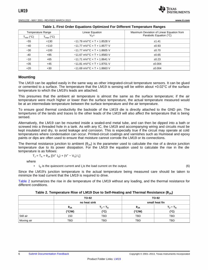
Using this procedure the best fit linear transfer function for many popular temperature ranges was calculated inTable 1. As shown in Table 1 the error that is introduced by the linear transfer function increases with widertemperature ranges.
Copyright © 2001–2013, Texas Instruments Incorporated Submit Documentation Feedback 5
Product Folder Links: LM19
LM19
SNIS122E –MAY 2001–REVISED MARCH 2013 www.ti.com
Table 1. First Order Equations Optimized For Different Temperature Ranges
Temperature Range Linear Equation Maximum Deviation of Linear Equation fromVO= Parabolic Equation (°C)Tmin (°C) Tmax (°C)
−55 +130 −11.79 mV/°C × T + 1.8528 V ±1.41
−40 +110 −11.77 mV/°C × T + 1.8577 V ±0.93
−30 +100 −11.77 mV/°C × T + 1.8605 V ±0.70
-40 +85 −11.67 mV/°C × T + 1.8583 V ±0.65
−10 +65 −11.71 mV/°C × T + 1.8641 V ±0.23
+35 +45 −11.81 mV/°C × T + 1.8701 V ±0.004
+20 +30 −11.69 mV/°C × T + 1.8663 V ±0.004
Mounting
The LM19 can be applied easily in the same way as other integrated-circuit temperature sensors. It can be gluedor cemented to a surface. The temperature that the LM19 is sensing will be within about +0.02°C of the surfacetemperature to which the LM19's leads are attached.
This presumes that the ambient air temperature is almost the same as the surface temperature; if the airtemperature were much higher or lower than the surface temperature, the actual temperature measured wouldbe at an intermediate temperature between the surface temperature and the air temperature.
To ensure good thermal conductivity the backside of the LM19 die is directly attached to the GND pin. Thetempertures of the lands and traces to the other leads of the LM19 will also affect the temperature that is beingsensed.
Alternatively, the LM19 can be mounted inside a sealed-end metal tube, and can then be dipped into a bath orscrewed into a threaded hole in a tank. As with any IC, the LM19 and accompanying wiring and circuits must bekept insulated and dry, to avoid leakage and corrosion. This is especially true if the circuit may operate at coldtemperatures where condensation can occur. Printed-circuit coatings and varnishes such as Humiseal and epoxypaints or dips are often used to ensure that moisture cannot corrode the LM19 or its connections.
The thermal resistance junction to ambient (θJA) is the parameter used to calculate the rise of a device junctiontemperature due to its power dissipation. For the LM19 the equation used to calculate the rise in the dietemperature is as follows:
TJ = TA + θJA [(V+ IQ) + (V+ − VO) IL]
where• IQ is the quiescent current and ILis the load current on the output. (6)
Since the LM19's junction temperature is the actual temperature being measured care should be taken tominimize the load current that the LM19 is required to drive.
Table 2 summarizes the rise in die temperature of the LM19 without any loading, and the thermal resistance fordifferent conditions.
Table 2. Temperature Rise of LM19 Due to Self-Heating and Thermal Resistance (θJA)
TO-92 TO-92
no heat sink small heat fin
θJA TJ − TA θJA TJ − TA
(°C/W) (°C) (°C/W) (°C)
Still air 150 TBD TBD TBD
Moving air TBD TBD TBD TBD
6 Submit Documentation Feedback Copyright © 2001–2013, Texas Instruments Incorporated
Product Folder Links: LM19

LM19
www.ti.com SNIS122E –MAY 2001–REVISED MARCH 2013
Capacitive Loads
The LM19 handles capacitive loading well. Without any precautions, the LM19 can drive any capacitive load lessthan 300 pF as shown in Figure 3. Over the specified temperature range the LM19 has a maximum outputimpedance of 160 Ω. In an extremely noisy environment it may be necessary to add some filtering to minimizenoise pickup. It is recommended that 0.1 μF be added from V+ to GND to bypass the power supply voltage, asshown in Figure 4. In a noisy environment it may even be necessary to add a capacitor from the output to groundwith a series resistor as shown in Figure 4. A 1 μF output capacitor with the 160 Ω maximum output impedanceand a 200 Ω series resistor will form a 442 Hz lowpass filter. Since the thermal time constant of the LM19 ismuch slower, the overall response time of the LM19 will not be significantly affected.
Figure 3. LM19 No Decoupling Required for Capacitive Loads Less than 300 pF
Table 3. LM19 with Filter for Noisy Environmentand Capacitive Loading greater than 300 pF
R (Ω) C (µF)
200 1
470 0.1
680 0.01
1 k 0.001
Either placement of resistor as shownabove is just as effective.
Figure 4. LM19 with Filter for Noisy Environmentand Capacitive Loading greater than 300 pF
Copyright © 2001–2013, Texas Instruments Incorporated Submit Documentation Feedback 7
Product Folder Links: LM19

R14.1V
R3
R20.1 PFU3LM4040
R4
VOUT
V+
VT
VTemp
+
-U1
LM19V+
U2
(High = overtemp alarm)
VT1
VT2
VTEMP
VOUT
VT1 =
R1 + R2||R3
(4.1)R2
VT2 =
R2 + R1||R3
(4.1)R2||R3
LM7211
LM19
SNIS122E –MAY 2001–REVISED MARCH 2013 www.ti.com
Applications Circuits
Figure 5. Centigrade Thermostat
Figure 6. Conserving Power Dissipation with Shutdown
Figure 7. Suggested Connection to a Sampling Analog to Digital Converter Input Stage
Most CMOS ADCs found in ASICs have a sampled data comparator input structure that is notorious for causinggrief to analog output devices such as the LM19 and many op amps. The cause of this grief is the requirement ofinstantaneous charge of the input sampling capacitor in the ADC. This requirement is easily accommodated bythe addition of a capacitor. Since not all ADCs have identical input stages, the charge requirements will varynecessitating a different value of compensating capacitor. This ADC is shown as an example only. If a digitaloutput temperature is required please refer to devices such as the LM74.
8 Submit Documentation Feedback Copyright © 2001–2013, Texas Instruments Incorporated
Product Folder Links: LM19

LM19
www.ti.com SNIS122E –MAY 2001–REVISED MARCH 2013
REVISION HISTORY
Changes from Revision D (March 2013) to Revision E Page
• Changed layout of National Data Sheet to TI format ............................................................................................................ 8
Copyright © 2001–2013, Texas Instruments Incorporated Submit Documentation Feedback 9
Product Folder Links: LM19

PACKAGE OPTION ADDENDUM
www.ti.com 10-Dec-2020
Addendum-Page 1
PACKAGING INFORMATION
Orderable Device Status(1)
Package Type PackageDrawing
Pins PackageQty
Eco Plan(2)
Lead finish/Ball material
(6)
MSL Peak Temp(3)
Op Temp (°C) Device Marking(4/5)
Samples
LM19CIZ/LFT4 ACTIVE TO-92 LP 3 2000 RoHS & Green SN N / A for Pkg Type LM19CIZ
LM19CIZ/NOPB ACTIVE TO-92 LP 3 1800 RoHS & Green SN N / A for Pkg Type -55 to 130 LM19CIZ
(1) The marketing status values are defined as follows:ACTIVE: Product device recommended for new designs.LIFEBUY: TI has announced that the device will be discontinued, and a lifetime-buy period is in effect.NRND: Not recommended for new designs. Device is in production to support existing customers, but TI does not recommend using this part in a new design.PREVIEW: Device has been announced but is not in production. Samples may or may not be available.OBSOLETE: TI has discontinued the production of the device.
(2) RoHS: TI defines "RoHS" to mean semiconductor products that are compliant with the current EU RoHS requirements for all 10 RoHS substances, including the requirement that RoHS substancedo not exceed 0.1% by weight in homogeneous materials. Where designed to be soldered at high temperatures, "RoHS" products are suitable for use in specified lead-free processes. TI mayreference these types of products as "Pb-Free".RoHS Exempt: TI defines "RoHS Exempt" to mean products that contain lead but are compliant with EU RoHS pursuant to a specific EU RoHS exemption.Green: TI defines "Green" to mean the content of Chlorine (Cl) and Bromine (Br) based flame retardants meet JS709B low halogen requirements of <=1000ppm threshold. Antimony trioxide basedflame retardants must also meet the <=1000ppm threshold requirement.
(3) MSL, Peak Temp. - The Moisture Sensitivity Level rating according to the JEDEC industry standard classifications, and peak solder temperature.
(4) There may be additional marking, which relates to the logo, the lot trace code information, or the environmental category on the device.
(5) Multiple Device Markings will be inside parentheses. Only one Device Marking contained in parentheses and separated by a "~" will appear on a device. If a line is indented then it is a continuationof the previous line and the two combined represent the entire Device Marking for that device.
(6) Lead finish/Ball material - Orderable Devices may have multiple material finish options. Finish options are separated by a vertical ruled line. Lead finish/Ball material values may wrap to twolines if the finish value exceeds the maximum column width.
Important Information and Disclaimer:The information provided on this page represents TI's knowledge and belief as of the date that it is provided. TI bases its knowledge and belief on informationprovided by third parties, and makes no representation or warranty as to the accuracy of such information. Efforts are underway to better integrate information from third parties. TI has taken andcontinues to take reasonable steps to provide representative and accurate information but may not have conducted destructive testing or chemical analysis on incoming materials and chemicals.TI and TI suppliers consider certain information to be proprietary, and thus CAS numbers and other limited information may not be available for release.
In no event shall TI's liability arising out of such information exceed the total purchase price of the TI part(s) at issue in this document sold by TI to Customer on an annual basis.

PACKAGE OPTION ADDENDUM
www.ti.com 10-Dec-2020
Addendum-Page 2


www.ti.com
PACKAGE OUTLINE
3X 2.672.03
5.214.44
5.344.32
3X12.7 MIN
2X 1.27 0.13
3X 0.550.38
4.193.17
3.43 MIN
3X 0.430.35
(2.54)NOTE 3
2X2.6 0.2
2X4 MAX
SEATINGPLANE
6X0.076 MAX
(0.51) TYP
(1.5) TYP
TO-92 - 5.34 mm max heightLP0003ATO-92
4215214/B 04/2017
NOTES: 1. All linear dimensions are in millimeters. Any dimensions in parenthesis are for reference only. Dimensioning and tolerancing per ASME Y14.5M.2. This drawing is subject to change without notice.3. Lead dimensions are not controlled within this area.4. Reference JEDEC TO-226, variation AA.5. Shipping method: a. Straight lead option available in bulk pack only. b. Formed lead option available in tape and reel or ammo pack. c. Specific products can be offered in limited combinations of shipping medium and lead options. d. Consult product folder for more information on available options.
EJECTOR PINOPTIONAL
PLANESEATING
STRAIGHT LEAD OPTION
3 2 1
SCALE 1.200
FORMED LEAD OPTIONOTHER DIMENSIONS IDENTICAL
TO STRAIGHT LEAD OPTION
SCALE 1.200

www.ti.com
EXAMPLE BOARD LAYOUT
0.05 MAXALL AROUND
TYP
(1.07)
(1.5) 2X (1.5)
2X (1.07)(1.27)
(2.54)
FULL RTYP
( 1.4)0.05 MAXALL AROUND
TYP
(2.6)
(5.2)
(R0.05) TYP
3X ( 0.9) HOLE
2X ( 1.4)METAL
3X ( 0.85) HOLE
(R0.05) TYP
4215214/B 04/2017
TO-92 - 5.34 mm max heightLP0003ATO-92
LAND PATTERN EXAMPLEFORMED LEAD OPTIONNON-SOLDER MASK DEFINED
SCALE:15X
SOLDER MASKOPENING
METAL
2XSOLDER MASKOPENING
1 2 3
LAND PATTERN EXAMPLESTRAIGHT LEAD OPTIONNON-SOLDER MASK DEFINED
SCALE:15X
METALTYP
SOLDER MASKOPENING
2XSOLDER MASKOPENING
2XMETAL
1 2 3
www.ti.com
TAPE SPECIFICATIONS
19.017.5
13.711.7
11.08.5
0.5 MIN
TYP-4.33.7
9.758.50
TYP2.92.4
6.755.95
13.012.4
(2.5) TYP
16.515.5
3223
4215214/B 04/2017
TO-92 - 5.34 mm max heightLP0003ATO-92
FOR FORMED LEAD OPTION PACKAGE

IMPORTANT NOTICE AND DISCLAIMER
TI PROVIDES TECHNICAL AND RELIABILITY DATA (INCLUDING DATASHEETS), DESIGN RESOURCES (INCLUDING REFERENCE DESIGNS), APPLICATION OR OTHER DESIGN ADVICE, WEB TOOLS, SAFETY INFORMATION, AND OTHER RESOURCES “AS IS” AND WITH ALL FAULTS, AND DISCLAIMS ALL WARRANTIES, EXPRESS AND IMPLIED, INCLUDING WITHOUT LIMITATION ANY IMPLIED WARRANTIES OF MERCHANTABILITY, FITNESS FOR A PARTICULAR PURPOSE OR NON-INFRINGEMENT OF THIRD PARTY INTELLECTUAL PROPERTY RIGHTS.These resources are intended for skilled developers designing with TI products. You are solely responsible for (1) selecting the appropriate TI products for your application, (2) designing, validating and testing your application, and (3) ensuring your application meets applicable standards, and any other safety, security, or other requirements. These resources are subject to change without notice. TI grants you permission to use these resources only for development of an application that uses the TI products described in the resource. Other reproduction and display of these resources is prohibited. No license is granted to any other TI intellectual property right or to any third party intellectual property right. TI disclaims responsibility for, and you will fully indemnify TI and its representatives against, any claims, damages, costs, losses, and liabilities arising out of your use of these resources.TI’s products are provided subject to TI’s Terms of Sale (www.ti.com/legal/termsofsale.html) or other applicable terms available either on ti.com or provided in conjunction with such TI products. TI’s provision of these resources does not expand or otherwise alter TI’s applicable warranties or warranty disclaimers for TI products.
Mailing Address: Texas Instruments, Post Office Box 655303, Dallas, Texas 75265Copyright © 2020, Texas Instruments Incorporated