ﻪﻤﯿﻤﺿ - popularphysics.ir · this content was downloaded on 23/01/2014 at 08:46 please...
TRANSCRIPT

www.popularphysics.ir
ضمیمه
ویژه نامۀ نانوفناوري 1392بهمن ماه
2008-1979:شابک
روش هاي آنالیز در شناسایی نانو مواد
آهنربا و نانوتکنولوژي
معــــرفی کتـاب
هاي سیلیکونی در دانشگاه تهرانرشد نانولوله
هاي نانوفناوري شامل نانوذرات آهن و اکسید آهنپژوهش
تحصیل در فناوري نانو
بهبود در تصفیۀ آب با اسفنج نانولولۀ کربنی
آزمایش نانو
هاي فلزي توسط فیزیکدانان تعیین تغییرات دما در نانوسیم
سرد ماندن در دنیاي نانوالکترونیک توسط داغ شدن
لطفا مقاالت خود را به آدرس نشریه پست نموده و یـا بـه . آدرس الکترونیکی ارسال نمایید تا به نام خودتان چاپ شـود
.نشریه در ویرایش مقاالت دریافتی مختار می باشد
.مقاالت دریافتی مسترد نخواهند شد
92بهمن
ضمیمۀ ماهنامه لذت فیزیک ویژه نامه نانوفناوري
1392بهمن ماه امیر راد: صاحب امتیاز، مدیر مسئول و سردبیر
مینا سعیدحسینی: معاون سردبیر و مدیر اجرایی راضیه حسینی اکبرنژاد: دبیر سرویس نانوفناوري
راضیه حسینی: صفحه بندي و اجرا
021– 8867 2727: تلفکس : آدرس
تهران ، پاسداران ، گلستان پنجم، میدان هروي ،خیابان 7شهید ضابطی ،کوچه سنبل، پالك
1667715881: کد پستی [email protected]: آدرس الکترونیکی
2

ویژه نامۀ نانوفناوري 3 92بهمن
واد
و می نان
سایشنا
در یز
آنالي
هاش
رو
(SEM)میکروسکوپ الکترونی روبشی
توان ها می در این روش . باشدهاي میکروسکوپی می هاي مختلفی جهت شناسایی و آنالیز مواد وجود دارد که یکی از معروف ترین آنها، روش امروزه روش هاي ترین روش هاي الکترونی است، از معروف که از گروه میکروسکوپ SEMمیکروسکوپ الکترونی روبشی . تصاویر بزرگنمایی شده از نمونه به دست آورد
رود که عالوه بر تهیۀ تصاویر بزرگنمایی شده، در صورتی که به تجهیزات اضافی مجهز شود می تواند براي آنالیز شیمیایی و دیگر میکروسکوپی به شمار میتواند پرتوهاي ساطع شده از این برهمکنش می . مبناي عملکرد این میکروسکوپ، برهم کنش پرتوي الکترونی با ماده است . ها نیز به کار گرفته شودبررسی
.جهت بررسی مورد استفاده قرار گیرد
قدرت تفکیک تصاویر . آید تا بتوان جزئیات آن را با دقت مطالعه نمود هاي میکروسکوپی، تصاویر با بزرگنمایی باال از ماده به دست می با استفاده از روش 1هاي نوري، قدرت تفکیکی در حدود به عنوان مثال، با استفاده از میکروسکوپ . شودمیکروسکوپی با توجه به نوع پرتوي مورد استفاده مشخص می
.و یونی با وضوح باال در حدود یک نانومتر تا چند آنگستروم قابل دسترسی است STM, AFMهاي الکترونی، نانومتر و در میکروسکوپ 200میکرومتر تا
در میکروسکوپ نوري شاید بتوان با تغییر انحناي سطح . اندهاي نوري توسعه پیدا کرده هاي الکترونی به دلیل محدودیت میکروسکوپ میکروسکوپهاي و تعداد آنها بزگنمائی تصاویر را به هر مقدار زیاد کرد، اما به علت بلند بودن طول موج نور، عمال تصاویر در بزرگنمائی ) میزان تقعر و تحدب(ها عدسیاي است که بتوان آنها را از هم کمترین فاصله بین دو نقطه (resolution) منظور از وضوح یاحد تفکیک . دهند وضوح خود را از دست می 2000باالي
میکرون دارند که این باعث محدودیت 0/2برابر و قدرت تفکیک 2000تا 1000هاي نوري معمولی، بزرگنمایی ماکزیمم، میکروسکوپ. تفکیک کرد برابر نیاز است که به وسیلۀ میکروسکوپ 10000هاي آلی به بزرگنمایی به عنوان مثال، براي دیدن ساختار سلول . استفاده از این دستگاه ها می شود
.نوري با طول موج امواج مرئی قابل دستیابی نیست
از آنجایی که طول موج . شود هاي الکترونی بجاي نور از پرتوي الکترونی استفاده می در میکروسکوپ تواند بسیار کوتاه باشد، پس در میکروسکوپ هاي الکترونی می توان به بزرگنمائی بسیار باال الکترون میهاي در واقع میکروسکوپ ). هاي الکترونی تا حد یک میلیون برابر در بعضی از میکروسکوپ(دست یافت
ها از لنزهاي کنند و مانند تمام میکروسکوپ الکترونی براساس قوانین امواج الکترومغناطیس کار می هاي الکترونی، به جاي نور از شار اند، با این تفاوت که در میکروسکوپ شیئ و چشمی تشکیل شده
ها عالوه بر این، لنـزها نیز در این میکروسکوپ. گرددپرانرژي استفاده می) پرتوهاي الکترونی(الکتـرون
هاي الکترونی ابداع شده، از نگاه تاریخی، اولین نوع از میکروسکوپ . باشند که با لنزهاي نوري متفاوت هستند از نوع لنزهاي الکترومغناطیس می باشد که مکانیزم عملکرد آن دقیقا مانند یک میکروسکوپ عبوري می (TEM:Transmission Electron Microscope) میکروسکوپ الکترونی عبوري
.شودنوري است، با این تفاوت که در آن به جاي نور از یک پرتوي الکترونی و به جاي لنزهاي نوري از لنزهاي مغناطیسی استفاده میگویند، یکی از انواع بسیار معروف میکروسکوپ هاي الکترونی است که Scanning Elecron Microscopeمیکروسکوپ الکترونی روبشی که به آن
گرددکه ماکس نول باز می 1935هاي روبشی به سال ها در زمینۀ توسعۀ میکروسکوپ نخستین تالش . کاربردهاي بسیاري در فناوري نانو پیدا کرده است
. از فوالد سیلیسیمی به دست آورد هاي الکترونیک نوري انجام داد و تصویري را بر اساس کانتراست کانالی الکترونی هایی در زمینۀ پدیدهدر آلمان پژوهشبا اضافه کردن سیم پیچ 1938و برهمکنش آن با نمونه انجام داد و توانست در سال SEM تحقیقات بیشتري را بر روي اصول فیزیکی مانفرد وان آردن
SEM استفاده از. حال دستگاه او از نظر عملی مورد استقبال قرار نگرفتبا این. ، میکروسکوپ الکترونی عبوري ـ روبشی بسازد TEMهاي روبشی به یک
توسط SEM توسعۀ بیشتر . در ایاالت متحدة آمریکا انجام شد 1942و همکاران در سال هاي ضخیم غیرشفاف اولین بار توسط ژورکینبراي مطالعۀ نمونه .براي اولین بار به صورت تجاري روانۀ بازار شد 1965و همکارش گري استوارت در دانشگاه کمبریج بریتانیا به انجام رسید و در سال پروفسور چارلز اتلی
شود تا از نمونه بمباران نمونه با پرتوي الکترونی سبب می .ها را به سادگی و با وضوح بیشتر مطالعه کنند سبب شد تا محققان بتوانند نمونه SEM ساختحرکت پرتو بر روي نمونه مجموعه اي از . شوندهایی خارج و به سمت آشکارسازها رها شوند که در آن قسمت تبدیل به سیگنال می ها و فوتون الکترون
. نمایش دهد تواند تصویر متقابل از سطح نمونه را به صورت لحظه به لحظه بر صفحه کند که بر این اساس میکروسکوپ می سیگنال ها را فراهم می .با میکروسکوپ هاي نوري کامال متفاوت است SEM بنابراین مکانیزم عملکرد
هاي جامد با وضوح و قدرت تفکیک و تمرکز بهتر در مقایسه با ، تهیۀ تصاویر میکروسکوپی به طور مستقیم از نمونه SEMدر ابتدا مزیت اصلی دستگاه هاي تجزیه و تحلیل، نظیر اشعه ایکس براي تعیین ترکیب اما بعدها قدرت اجرایی و عملیاتی دستگاه توسعه یافته و به روش . هاي نوري بود میکروسکوپ
. جهت تشخیص وضعیت بلوري مجهز گردید (electron channeling) هاي الکترونیشیمیایی و کانال edu.nano.irمنبع
مهدي مشرف جوادي، محمد هادي مقیم: نویسندگان
ویژه نامۀ نانوفناوري 4 92بهمن
دانشمندان نانوتکنولوژي در حال انجام پژوهش براي تعیین این هستند که نانوذرات چگونه می توانند براي قویتر
این . کار گیري مواد کمتر استفاده شوند کردن آهنرباها با به تحقیقات بر روي نئودیوم، آهن و بورون که همگی در تولید آهنربا
استفاده می شوند در حال انجام .است
نئودیوم عنصري است که براي قوي ساختن آهنربا مورد
پذیرفتاري . گیرداستفاده قرار میمغناطیسی نئودیوم با توجه به
یک آهنربا توسط به . شودچینش الکترونها در مدار هر اتم تعیین می هاي جفت نشده در میدان مغناطیسی خط شدن اسپین الکترون
هر اتم نئودیوم، هفت الکترون جفت نشده دارد که . شودتشکیل می . توانند براي تبدیل قسمتی از این ماده به آهنربا به خط شوند می
شود، زمانیکه نئودیوم در یک آلیاژ همراه با آهن و بورون استفاده می آهنرباهاي قوي در تمام ادوات . دهدنتیجۀ کوچکی نشان می
هاي ساخت آهنربا قابلیت. گیرندالکترونیکی مورد استفاده قرار می توان ها را می یکی از دالیلی است که ادوات الکترونیکی مثل لپ تاپ
.کوچک و با وزن کم ساختتوان نئودیوم یک عنصر نادر خاکی است؛ از دیگر عناصر این دسته می
در حالت طبیعی . ساماریوم، دیسپروسیوم و پراسئودیمیوم را نام برد .شونداین عناصر به صورت ترکیب با عناصر دیگر یافت می
ترکیب بودن با عناصر دیگر به این معنی است که آنها باید استخراج و تخلیص شوند، که فرآیند استخراج خطر آلودگی محیط زیست را به
به دلیل این عوارض، نگرانی براي کمبود عرضه از این .آوردارمغان میتواند تاثیري جدي در تولید صنعتی ایجاد عناصر وجود دارد که می
.کند
پژوهشگران با استفاده از نانوذرات نئودیوم در حال ساخت آهن این پژوهش در . رباهایی هستند که نئودیوم کمتري نیاز داشته باشد
مراحل اولیه است، اما ایده این است که با استفاده از نانوذرات نئودیوم شود، تر می هاي مختلف قوي و مواد دیگر از قبیل آهن، اتصال بین اتم
تر همراه با استفادة کمتر مواد حاصل در نتیجه میدان مغناطیسی قوي .شودمی
آهنربا و نانوتکنولوژي
منبع Nanotechnology For Dummies, 2nd Edition Earl Boysen, Nancy, C. Muir
حسینی. مترجم ر
خواص، روشهاي : آشنایی با نانو ذرات: نام کتاب تولید و کاربرد
عبدالرضا سیم چی: نویسنده
دانشگاه صنعتی شریف: انتشارات
صفحه 280 -1387: تعداد صفحات/سال انتشار
از آنجا که خواص مواد در مقیاس نانو به نـحـو : در مقدمه کتاب آمده است کند، نانو فناوري پنجره اي جدید به دنیاي مواد باز نموده مطلوبی تغییر می
که محصول آن امکان ساخت مواد و تجهیزاتی با کارایی بیشتر است و نانـو هدف این کتاب معرفی نانـو . ذارت در مرکز توجه بیشتر محققین قرار دارد
.ذارت و کاربردهاي آنهاستاین کتاب براي دانشجویان فیزیک، شیمی و عالقه مندان بـه عـلـم نـانـو
در فصل اول این کتاب تاریخچه اي از نانو فناوري نیـز ارائـه . مناسب است .شده است
:فصل دارد 8این کتاب
دیباچه
آشنایی با مواد نانو ساختار
روشهاي شناسایی و آنالیز
خواص نانو ذارت
فرآوري نانو ذرات در مایعات با روشهاي شیمیایی
فرآوري نانو ذارت در گازها
فرآوري نانو ذارت به روش مکانیکی
بازار
ی کتـابمعــــرف
ویژه نامۀ نانوفناوري 5 92بهمن
عنوان کاتالیست رشد، امکان رشد نانوساختارهاي پژوهشگران دانشگاه تهران با استفاده از ترکیب دو ماده طال و نیکل به هاي ي این محققان قبال براي تولید نانوسیم وسیله روش استفاده شده به. سوراخدار و توخالی را محقق ساختند
.سیلیکاتی مورد استفاده قرار گرفته بود اما امکان رشد این نانوساختار تاکنون انجام نپذیرفته استاین مقاله بخشی از کار پایان نامه دوره کارشناسی ارشد دو تن از ” : دکتر مهاجرزاده در مورد این تحقیقات گفت
دانشجویان بنده بوده است و در واقع بخشی از یک کار بزرگتر در راستاي ایجاد ترانزیستورهاي عمودي اثر میدان البته گذر ذرات کوچک . ها دارد و حساسیت به مقدار بار آن DNAهاي کوچک مانند با قابلیت گذردهی المان هاي به هر حال هدف ساخت نانولوله . ها نقش داشته باشد تواند در مقدار جریان آن مانند نانوذرات نیز می
“.سیلیکانی است و نیز با استفاده از رشد به روش Templateهاي سیلیکانی بدون هدف اصلی این تحقیقات بر پایه ایجاد نانولوله
VLS (Vapor-Liquid-Solid) یاSLS (Solid-Liquid-Solid) هاي سیلیکانی ها قبال براي ایجاد نانو سیم این در حالی است که این روش . بوده استعنوان کاتالیست رشد؛ با استفاده از ترکیب دو ماده طال و نیکل به . اند استفاده شده بودند اما امکان رشد نانوساختارهاي سوراخدار و توخالی محقق نشده
.این عمل محقق شده استهاست که ایجاد هاي کربنی سال ذکر است که نانولوله الزم به . اند پذیر و نسبتا آسان ایجاد شده هاي سیلیکانی به روش بسیار تکرار در این پروژه نانولوله
فرد سیلیکان از آینده خوبی برخوردار دلیل خواص منحصر به از طرف دیگر این ساختارها به . هاي سیلیکانی محقق نشده است شوند ولی ایجاد نانولوله میي وسیله به )Unzip(ها قابلیت بازشدن به عالوه این نانولوله . ها است ي آن وسیله هستند که از آن میان ساخت نسبتا آسان ترانزیستورهاي اثر میدان به
لذا ساخت . گردد را دارند جریان الکترونی که در میکروسکوپ الکترونی استفاده می در مجموع این روش بر اساس استفاده هوشمندانه از . هاي سیلیکانی نیز آسان است نانونوار
تواند نقش خود را در ایجاد لوله دو کاتالیست طال و نیکل است و هر کدام از این ترکیب میهنوز هم موارد بسیار زیادي ناشناخته هستند که . هاي سیلیکان بازي کند و یا انتقال اتم
.نیاز به زمان بیشتري داردبستر مورد استفاده سیلیکون با جهت ” : وي با اشاره به مراحل انجام این تحقیقات گفت
است که بعد از تمیز کردن در مراحل مختلف عملیات الیه نشانی انجام ) 100(بلوري هایی در مقیاس چند نانومتري هاي طال و نیکل به ضخامت الیه نشانی منظم الیه . گردد میوسیلۀ سامانۀ صورت دو الیه و یا چند الیه از مسائل کلیدي این پروژه بوده است که به به
که همان الیه نشانی بخار شیمیایی در LPCVDبعد از الیه نشانی الیۀ دو فلزي نمونه در دستگاه . بخار فیزیکی به کمک اشعۀ الکترونی محقق شده است. گردد هاي سیلیکانی محقق می گراد امکان رشد نانولولهدرجه سانتی 500الی 400فشار پایین است قرار داده شده است که با انجام رشد در دمایی در حد
“.توان از گاز هیدروژن و سیالن استفاده کرد ذکر است که در زمان رشد میالزم بههایی با قطر بسیار کم و نیز به گفتۀ مهاجرزاده، در صورتیکه بتوان لوله . صورت مستقیم در الکترونیک و بیوالکترونیک کاربرد دارد نتایج این تحقیقات به
در اینصورت با عبور هر گونه . شناور از درون محقق خواهد شد ) کنترل کننده (طول مناسب ایجاد کرد امکان ساخت ترانزیستورهاي اثر میدان با گیت توان با توجه به ابعاد بسیار کوچک این قطعه می . گیري خواهد بود جریان ترانزیستور تغییر کرده و قابل اندازه DNAموجود بسیار کوچک و باردار مانند
DNA صورت همراستا در آورد تا اطالعات مربوط به را بهSequencing تکمیل گردد. در صورت موفقیت کامل این پروژه ” : مهاجرزاده در پایان سخنان خود با اشاره به ادامه یافتن این تحقیقات و ابراز امیدواري از آینده نتایج آن افزود
البته . داشته باشد تواند در زمینه بیوالکترونیک کاربرد تواند پل ورود کشور به عرصه نانوالکترونیک باشد زیرا عالوه بر کاربرد در ادوات الکترونیکی می می “.ذکر است که بخشی از این تحقیقات در دست انجام است و در مراحل ثبت است و امکان ارائه دقیق مطالب وجود نداردالزم به
به ت، نتایج این کار تحقیقاتی که به دست مهندس محمد تقی نژاد و مهندس حسین تقی نژاد، دکتر محمد عبداالحد و دکتر مهاجرزاده صورت گرفته اس ISIقابل ذکر است که یکی از نتایج اخیر این پژوهش در قالب مقاله . عنوان یکی از چند مقاله برتر در ستاد ویژه توسعه فناوري نانو نیز انتخاب شده است
.منتشرشده است) 897-889، صفحات 2013، سال3، شماره 13جلد ( Nano lettersدر مجله
رشد نانولوله
هاي سیلیکونی در دانشگاه تهران
منبعwww.nano.ir

ویژه نامۀ نانوفناوري 6 92بهمن
نانوذرات به قدري کوچکند که تنها شامل چند تا چندهزار اتم هستند در مقابل . اي در ابعاد نانو، نانوذره نام دارد هر ماده .هاي منحصر به فردي داشته باشندشود نانومواد ویژگیاین تفاوت در اندازه سبب می. توانند شامل میلیاردها اتم باشندمواد حجمی که می
همچنین در آب و در خون وجود دارد که به انتقال اکسیژن کمک می . کاربرد دارد ... ها و ها و ساختمان آهن عنصري است که به طور روزمره در اتومبیل .کند
دانیم هنگامیکه با اکسیژن شود و همانطور که می آهن یکی از موادي است که به دلیل وضعیت الکترونها در مدار اتمهایش براي ساختن آهنربا استفاده می .مشخص شده که نانوذرات آهن و اکسید آهن، هر دو بسیار مفیدند. ترکیب شود اکسید آهن ایجاد شده و زنگ میزند
توسط نانوذرات (MRI)بهبود تصویربرداري تشدید مغناطیسیاگر آهن در باران رها شود، زنگ خواهد زد و زنگ از اکسید آهن تشکیل شده است، مولکولی که شامل سه اتم آهن و
.چهار اتم اکسیژن استآهن چهار الکترون جفت نشده دارد در حالیکه اکسید آهن فقط دو . اکسید آهن هم مثل آهن، خواص مغناطیسی دارد
کنند، اکسید آهن کمتر از آهن، به دلیل اینکه الکترونهاي جفت نشده ماده را مغناطیسی می . الکترون جفت نشده داردخاصیت پارامغناطیسی نانوذرات اکسید آهن با . اکسید آهن یک مادة پارامغناطیسی است . خاصیت مغناطیسی دارد
.توانند به جاهایی بروند که ذرات بزرگ نمی توانندحالت حجمی تفاوتی ندارد به جز اینکه این ذرات کوچک میاگر نانوذرات پارامغناطیسی به جسمی که از آن تصویر گرفته (MRI)براي مثال، در تصویربرداري تشدید مغناطیسی
-هایی که جذب سلول براي این منظور محققان نانوذرات اکسید آهن را توسط پوشاندن آنها با مولکول . شود متصل شوند، تصویر بهتري خواهیم داشت می .شوند عامل دار کردند تا تصاویر بهتري تهیه شودهاي سرطانی می
تومورها را بهبود می بخشد MRI اي از نانوبلورهاي اکسید آهن احاطه شده با سیلیکون نانومتخلخل است، نه تنها تصاویرساخت نانوذراتی که شامل هسته .دهدبلکه به محققان توانایی کنترل براي آزاد سازي داروها را می
هاي زیر زمینی با نانوذرات آهنتصفیه آبشود نانوذرات آهن براي این خاصیت سبب می . این نانوذرات مغناطیسی میزان سطح زیادي دارند . نانوذرات آهن خواص مغناطیسی آهن را دارا هستند
.هاي زیرزمینی مفید باشندهاي آبتصویربرداري پزشکی و تصفیۀ آالیندههاي خود توانند الکترون هاي زیرزمینی مفید هستند زیرا می هاي آلی آب نانوذرات آهن در پاکسازي آالینده
هاي آلی را هایی که آالینده هاي کلر بدهند که در بسیاري از مولکول را به اتم هاي الکترونگاتیوتر مثل اتم .سازند، حضور داردمی
به این دلیل که نانوذرات . ضرر شودها به ترکیبات بیتواند سبب شکستن مولکولها میبخشیدن این الکترونهاي زیرزمینی براي مدت طوالنی معلق باقی بمانند و به سراسر سیستم انتقال یابند، براي توانند در آب می
.گیرندهاي زیرزمینی مورد استفاده قرار میمحدودة بزرگی از آبمحققان در مراحل بعدي استفاده از نانوذرات اکسید آهن در حال بررسی استفاده از نانوذرات آهن براي
:تصویربرداري و درمان هستند که شامل موارد زیر استتواند توسط یک میدان مغناطیسی در با استفاده از نانوذرات شامل هستۀ آهنی، دارو می : دارورسانی هدفمند
. اي خاص از بدن بیمار، هدایت شودمحدودهاند، یک میدان الکترومغناطیسی نشان داد نانوذرات در محدودة بیماري تجمع کرده MRIپس از اینکه تصویر : و درمان MRI بهبود تصویربرداري
.کندهاي بیمار، ایجاد حرارت میشود، که براي نابود کردن سلولنوسانی براي به ارتعاش درآوردن نانوذرات استفاده می
پژوهش
هاي نانوفناوري شامل نانوذرات آهن و اکسید آهن
منبع Nanotechnology For Dummies, 2nd Edition Earl Boysen, Nancy, C. Muir
حسینی. مترجم ر

ویژه نامۀ نانوفناوري 7 92بهمن
تحصیل در فناوري نانو یعنی . اي است رشته هاي تحصیلی نیست، بلکه یک حوزة بین اي جدا و مستقل از دیگر رشته ي فناوري نانو رشته رشتهخواهد در این زمینه تحصیل کند نیاز کسی که می . گیري از این رفتارها ها در مقیاس نانو و کنترل و بهره توانمندي در درك رفتار مواد و سیستم
ا شناسی دید داشته باشد و ثانیا بتواند تعامل علمی خوبی ب هاي مهندسی، فیزیک، شیمی یا زیست است اوال نسبت به مبانی علمی یکی از حوزه .ها برقرار کند متخصصان سایر رشته
ي کارشناسی را در یکی از کسی که دوره . ي کارشناسی در آنهاست ها مستلزم گذراندن حداقل دوره فراگیري مبانی علمی هریک از این رشته هاي مختلف فیزیک، شیمی و زیست را درك کند و در رسد که بتواند ارتباط حوزه هاي مهندسی یا علوم گذرانده باشد، به حدي از دانش می رشته
.هاي مختلف همکاري کند تحقیقات تیمی با افرادي با تخصصکه ) ازجمله ایران (از این رو در اغلب کشورها . پذیر است بنابراین تحصیل رسمی در فناوري نانو در مقاطع کارشناسی ارشد و دکتري امکان
.شود آموزش رسمی فناوري نانو دارند، این رشته صرفا در مقاطع تحصیالت تکمیلی ارائه میازجمله دانشگاه تهران، تربیت مدرس، شریف، پژوهشگاه دانشهاي بنیادي، امیرکبیر، صنعتی شاهرود، کاشان، (هاي کشور هم اکنون برخی دانشگاه
هاي از رشته . هاي مختلف دانشجو دارند در مقاطع کارشناسی ارشد و دکتري فناوري نانو در گرایش ) صنعتی سهند، پژوهشگاه مواد و انرژي هاي مهندسی الکترونیک، مهندسی توان به نانوشیمی، نانوفیزیک، نانو فیزیک محاسباتی و رشته شود می ها ارائه می مختلفی که در این دانشگاه
ها مشخص است، دانشجویان طور که از عنوان این رشته همان. شیمی، مهندسی مواد، مهندسی مکانیک و مهندسی پلیمر با گرایش نانو اشاره کرد .توانند در فناوري نانو ادامه تحصیل دهند هاي فنی و علوم می اغلب رشتهثانیا . توان به طور خالصه نتیجه گرفت که براي تحصیل رسمی در فناوري نانو اوال نیاز است حداقل مدرك کارشناسی داشته باشید بنابراین می
.ي شخص صورت گیرد ي خاصی تحصیل کرده باشید، بلکه انتخاب رشته در سطح کارشناسی باید برحسب عالقه نیاز نیست که حتما در رشتهدر توانند بدون اینکه تحصیل رسمی در فناوري نانو داشته باشند، فعالیت پژوهشی خود هاي علوم انسانی می اما دانشجویان و عالقمندان به رشته
زیرا توسعۀ فناوري نانو در کنار مباحث فنی و تکنیکی نیازمند . هاي مرتبط با فناوري نانو انجام دهند سطح کارشناسی ارشد و باالتر را در حوزه هاي نوین ي فناوري شناسی و آموزشی ازجمله مباحث مهم در توسعه مطالعات مدیریتی، حقوقی، جامعه . هاي فکري و مدیریتی است زیرساخت
. همچون فناوري نانو است منبع
www.nano.ir
تحصیل در فناوري نانو

ویژه نامۀ نانوفناوري 8 92بهمن
هاي آب ور کردن آالینده هاي قبلی قادر به غوطه اخیرا یک اسفنج نانولولۀ کربنی که بیش از سه برابر تالش .ها، کودهاي شیمیایی و مواد دارویی است، معرفی شده استمانند آفت کش
هاي نانولولۀ کربنی، به طور منحصر به فردي با گوگرد آالییده شدند، همچنین ظرفیت باالي آنها اسفنج
.دهداي براي حوادث صنعتی و پاکسازي نشت نفت ارائه میبراي جذب نفت پتانسیل بالقوههاي کربنی داراي خواص با توجه به ساختار آنها، نانو لوله . اندهاي کربنی ساخته شده اي توخالی هستند که از الیه هاي کربنی ساختارهاي استوانه نانولوله
.هاي خورشیدي منجر شده استهاي کاربردي از محافظت بدن تا پنلاي از برنامهاي هستند که به مجموعهحرارتی، شیمیایی و مکانیکی فوق العادهعنوان یک کاندید عالی براي تصفیۀ همچنین این ماده، اگرچه ساختن آن به شکل یک پودر ریز و نهایتا بازیابی آنها از آب با مشکالتی مواجه است، به
. استها شناخته شدهپساببراي از بین بردن نفت ریخته CNTاستفاده از پودر ": گویدنویسندة این مقاله از دانشگاه رم، می
توانند از دست بروند یا کار بردن آنها سخت است و در نهایت می به. شده در اقیانوس، دشوار است ".در اقیانوس پراکنده شوند
هاي کربنی در مقیاس میلی متري و یا سانتی متر، که ما در این مطالعه با این حال، نانو لوله "آنها به دلیل ساختار متخلخل در آب شناور شده و با .شوندتر استفاده می ایم، بسیار آسان ساخته
شود و سپس نفت رها می با فشردن سادة آنها . شوندشوند و به راحتی برداشته می نفت اشباع می ".توانند دوباره استفاده شوندمی
ها را به اندازة الزم در مطالعۀ جدید، محققان با افزودن گوگرد درحین فرآیند تولید، نانولوله .میلی متر دارد20حجیم کردند؛ اسفنج نتیجه شده طول حدود
شود که فروسنس را می CNT هايگیري سطح اسفنج افزودن گوگرد منجر به نقایصی در شکل هاي کربنی اضافه که در طول فرآیند تولید براي جانشینی آهن در فضاي خالی داخل نانولوله
.کندشده، فعال میهاي CNT طور مغناطیسی کنترل شوند و بدون تماس مستقیم به حرکت درآیند که مشکل کنترل توانند به ها می حضور آهن به این معناست که اسفنج
.دهداضافه شده به سطح آب را کاهش می-، حالل آلی سمی دي کلروبنزن را با موفقیت از آب می CNTاند که چگونه اسفنج محققان شرح داده
همچنین مشاهده شده که روغن نباتی را بیشتر . هاي قبلی دارد برابر بیشتر از روش 3/5زداید و جذب .کنندهاي قبلی جذب میبرابر وزن اولیۀ خود و روغن موتور را با ظرفیت کمی باالتر از گزارش 150از -نفت یا حالل. ها استCNTخواص جذب بهبود یافتۀ اسفنج به دلیل ساختار متخلخل و سطح خشن"
-ها جذب شوند و سطوح زبر این امر را آسانتر مـی CNTتوانند به سادگی در فضاي خالی درون ها می. ها براي تولید در مقیاس تـجـاري اسـت مرحلۀ بعدي این پژوهش بهبود فرآیند ساخت اسفنج . سازند
.ها را بررسی کنیمهمچنین باید قبل از هرگونه برنامۀ کاربردي جهانی سمیت این اسفنج
بهبود در تصفیۀ آب با اسفنج نانولولۀ کربنی
منبعhttp://www.sciencedaily.com

ویژه نامۀ نانوفناوري 9 92بهمن
انوش ن
مایآز
تولید الگوهاي نانو با استفاده از روش لیتو گرافی
در روش ساخت از باال به پایین، از شیئی . تولید از باال به پایین و تولید از پایین به باال : گیرنددانشمندان براي ساخت اشیاي نانویی از دو روش بهره می در روش ساخت از پایین به باال، شیء در ابعاد نانو را اتم . برند تا قطعاتی در ابعاد نانو ایجاد کنند تري میکنند و آن را در قطعات کوچکبزرگ استفاده می
.سازند تا به اندازة مورد نظر برسندبه اتم میروز طول 12متر را به قطعاتی با ضخامت نانو برش بزنیم، و اگر براي تولید هر برش یک ثانیه وقت الزم باشد، اگر یک سکه به ضخامت تقریبی یک میلی
.می کشد تا کل سکه را در ابعاد نانو برش بزنیماگر براي هر اتم طال یک ثانیه . نانو متر ایجاد کنید 13خواهید یک ذرة طالي کروي با قطر حاال تصور کنید که با در کنار هم گذاشتن اتم به اتم طال می
.وقت الزم داشته باشید، براي تولید یک نانو ذره از طال به یک روز وقت احتیاج داریدکشد تا ذرات مورد نیاز ها به هزاران ذره از این نانو ذرات احتیاج دارند، تقریبا یک سال طول می به دلیل این که دانشمندان براي انجام برخی از آزمایش
گیرند که همزمان تعداد بسیار زیادي از نانو ذرات بنابراین به منظور جلوگیري از اتالف زمان، روش هایی را به کار می . براي انجام یک واکنش تامین شود .تولید شوند
در این حالت، از روش ساخت پیوسته براي تولید نانو . کنیمها به تعداد کمی از نانو ذرات با شکل، ابعاد و ترکیب مشخص نیاز پیدا می در برخی از آزمایشگیرند؛ چیزي شبیه نوشتن با یک خودکار که در هر مرحله این ساختارها، به صورت یکی در یک مرحله، شکل می . شودساختارهاي مجزا بهره گرفته می
.یک مقدار جوهر روي کاغذ نقش می بندد-ها، به تعداد بسیار زیادي از نانو ذرات با شکل، اندازه و ترکیب یکسان نیاز داریم که در این صورت،کاربرد روش هم زمان مؤثر واقع می در سایر آزمایش
.کنند تقریبا چیزي شبیه یک سینی از یخ هاي مکعبیدر این روش تعداد زیادي از نانو ذرات با ابعاد و اشکال مشخص را به طور هم زمان تولید می. شود. گیردها به عنوان قالب مورد استفاده قرار می در این روش یک الیه از نانو گوي . آوردها، نانو ذراتی با شکل و ترکیب مطلوب به وجود می چاپ نانو گوي
ها برداشته کنند و سپس با استفاده از یک حالل، نانو گوي هاي در کنار هم قرار گرفته، بر روي سطح زیرین رسوب می هاي بین گوي مواد از طریق حفره کند و ها را تعیین می هاي میان گوي ها در کنار هم، آرایش حفره نحوة قرار گرفتن نانو گوي . مانندشوند و تنها مواد رسوب کرده بر روي سطح باقی می می
.گیردمتعاقب آن، الگوي نانو ساختار شکل میسانتی متر براي تهیۀ الیه اي از نانو گوي ها بهره بگیرید و از 2هاي نایلونی با قطر از گوي . در این فعالیت شما شاهد نمایشی از چاپ نانو ذرات هستید
.دهدکند و در نهایت، الگوي ذرات مورد نظر را شکل میها عبور و بر روي سطح زیرین رسوب میپودر تالک به عنوان ماده اي استفاده کنید که از حفره اهداف فعالیت
کند که از چاپ نانو گویها، گیرد و مشاهده می هاي پیوسته و هم زمان تولید اجسام نانویی را فرا می در این فعالیت، پژوهشگر مفاهیم اساسی و کلی روش .این فرآیند در واقع شبیه سازي همان روش تولید هم زمان نانو اجسام در مقیاس بزرگ است. شودبراي ساخت الگویی از ذرات نانو استفاده می
وسایل مورد نیاز 4 عدد میلۀ کار دستی
دو گیرة کاغذي
چسب
پودر تالک
کاغذ تمیز چسب دار
قیچی
10 سانتی متر 2گلولۀ پالستیکی یا تیله با قطر
نوار و یک برگ کاغذ سیاه رنگ کار دستی
10 سانتی متر 8گلولۀ پالستیکی یا تیله با قطر
مراحل فعالیت .اجازه دهید تا چسب خشک شود. میله، یک مثلث متساوي االضالع بسازید 3با استفاده از چسب و -1 بر چسب را از پشت قطعۀ چسب دار بردارید و . سانتی متر از کاغذ چسب دار و کاغذ سیاه برش بزنید 5/12× 5/12یک قطعه مربعی شکل با ابعاد -2
. با نوار چسب، گوشه هاي کاغذ را بر روي سطح محکم کنید. جلوي کاغذ را روي سطح بگذارید؛ به طوري که سطح چسبناك آن به طرف باال باشد

ویژه نامۀ نانوفناوري 10 92بهمن
انوش ن
مایآز
.را روي کاغذ چسب دار قرار دهید) 1(اکنون قالب تهیه شده از مرحله ي
اگر در قالب مثلثی، هم چنان . سانتی متري در قالب مثلثی قرار دهید تا یک سیستم انباشته به وجود آید 2هاي تا جایی که ممکن است، از گلوله -3 .توانید با استفاده از یک میلۀ دیگر، مساحت قالب مثلثی را کاهش دهیدفضاي خالی باقی مانده است، می
مراقب باشید پودر . پاش، مقداري از پودر تالک را از باال روي قالب مثلثی بپاشید تا الیه اي نازك از پودر تالک روي قالب پخش شود با استفاده از نمک -4 .پاشیدن پودر تالک را به این روش چندین بار تکرار کنید تا طرح واضحی روي تمام سطح چسبناك کاغذ به وجود آید. تالک را تنفس نکنید
سپس . ها نشسته است، روي سایر قسمت هاي کاغذ چسب دار نپاشد مراقب باشید، پودر تالکی که روي سطح فوقانی گلوله . ها را بردارید قالب و گلوله -5شود تا از طرح به این کار باعث می . کاغذ سیاه رنگ را روي کاغذ چسب دار بگذارید، به طوري که چیزي شبیه به سانویچ مربع شکل به وجود آید
با استفاده از گلوله هاي هم اندازه یا متفاوت می توانید الگوهاي دیگري تهیه کنید و با استفاده از قالب هایی که شکل . وجود آمده محافظت شود .به طرح هاي زیر توجه کنید. هاي گوناگونی دارند، طرح هاي متفاوتی به وجود آورید
پرسش .هاي ایجاد شده را بیان کنیدها و طرحرابطه کیفی موجود بین آرایش سیستم انباشتۀ گوي -1
با استفاده از روابط هندسی، درصد فضاي اشغال شده و اشغال نشده در سیستم انباشتۀ گلوله ها را -2 .در قالب مثلثی شکل محاسبه کنید
؟)سریال(است یا روش پیوسته ) موازي(روش به کار برده شده در این آزمایش، روش هم زمان -3
-ها، بهره می هاي متفاوت براي تهیۀ یک قالب تک الیه اي از گلوله زمانی که از دو نوع گوي با اندازه -4 کنید؟گیرید، چه تغییري را مشاهده می
اطالعات بیشتر هایی که ما در این فعالیت با آن ها سرو کند اما اندازه هاي فناوري ساخت در ابعاد نانو را شبیه سازي می فعالیتی که شرح دادیم یکی از تکنیک
.کار داریم، بسیار بزرگ تر از چندین نانومترند
به جاي پودر تالک می توان تخته . این نکته که فقط یک الیۀ نازك از پودر تالک را باید بر روي کاغذ چسب دار بپاشید، بسیار تعیین کننده است .ها تکان داد تا الیه اي نازك از گچ روي کاغذ چسب دار بپاشدکن هاي گچی را روي گلولهپاك
هاي متفاوت در کنار هم، هایی با اندازه هاي روي هم، و گوي هاي چند تایی از گوي هاي گوناگون، الیه توانید، با استفاده از قالب هم چنین می .الگوهاي گوناگونی تهیه کنید
توانید، به جاي پودر تالک و کاغذ چسب دار، از منبع نور ماوراء بنفش و کاغذ هاي حساس به نور براي اینکه آزمایش مشابهی ترتیب دهید می .کندگذرد و روي کاغذ حساس به نور، الگویی را از ساختارهاي مشابه طراحی میها میهاي بین گلولهنور ماوراء بنفش از حفره. استفاده کنید
ها در حال حاضر در مرحلۀ آزمون کارایی و هاي متفاوتی براي ایجاد نانو ساختارها پیدا کرده اند، اما این روشهاي اخیر، دانشمندان روشدر سالشود، مشابه هاي رایانه و تمام مدارهاي مجتمع به کار گرفته می فوتولیتوگرافی، فناوري جدیدي که امروزه براي ساخت پردازنده . توانمندي اند
.همین روشی است که شما آن را تجربه کردید
پاسخ پرسش ها. آیدآورند، در هر مکانی که سه گوي به یکدیگر نزدیک شده اند، یک حفرة سه گانه به وجود می شوند و سیستم انباشته را به وجود میها به هم نزدیک میوقتی گوي -1
ها در کنار یکدیگر، الگویی از رسد و بر اساس آرایش گويشود، پودر تالک تنها از طریق این حفره ها به سطح کاغذ میها پاشیده میزمانی که پودر تالک روي گوي .آوردیک ساختار پدید می
زمانی که ). مجذور شعاع کره × π× تعداد گلوله ها ( ، و سپس مساحت اشغال شده توسط گوي ها را محاسبه کنید ) 1/2× ارتفاع× طول (ابتدا مساحت قالب مثلثی -2درصد از مساحت زیرین گلوله ها نمایان 7/2درصد از مساحت قالب مثلثی توسط گوي ها اشغال می شود و 92/8ها به صورت مستقیم انباشته در می آیند، گوي .است
هاي منفردي تر از شکلاین اتفاق سریع. کندهاي مشخصی را نمایان میها، هم زمان شکلپاشیدن پودر روي گوي. روش به کار برده شده، همان فرایند هم زمان است -3 )فرایند پیوسته یا سریال. (آینداست که هر کدام در یک مرحله و مجزا به وجود می
توان الگوهاي جدیدي را از این طریق با وجود این بی نظمی، می. شودخوش تغییر میهاي متفاوت، آرایش منظم سیستم انباشته دستهایی با اندازهبا استفاده از گوي -4 .تهیه کرد
:منبع آزمایش هاي ساده نانو، نوشتۀ علیرضا منسوب بصیري

ویژه نامۀ نانوفناوري 11 92بهمن
هاي فلزي توسط فیزیکدانان تعیین تغییرات دما در نانوسیم
کنش بین نور و افت و خیز بار در نانوساختارهاي فلزي که پالسمون نام دارد، فیزیکدانان قابلیت اندازه گیري تغییرات دما در ناحیۀ سه با استفاده از برهم .توان به عنوان یک موج الکترونی در سطح فلز در نظر گرفتپالسمون را می. دهندبعدي بسیار کوچک فضا را نشان می
به Nano Lettersژورنال ” "Thermoplasmonics: Quantifying Plasmonic Heating in Single Nanowiresاي با عنواناین پژوهش در مقاله . چاپ رسیده است
. هاي طال، یک نانوساختار پالسمونی ساخته شددر این آزمایش توسط لیتوگرافی باریکۀ الکترونی و تمرکز دقیق یک لیزر بر نانوسیم-تغییر در مقاومت به تغییر دماي نانوسیم مربوط می . گیردشود، اندازه می این کار تغییر در مقاومت الکتریکی یک نانوسیم طال را هنگامیکه نوردهی می
گیري تغییرات دما در حجم نانویی مشکل است، و تعیین اینکه چه بخشی از تغییرات دما ناشی از پالسمون هاست می تواند بیشتر به توانایی اندازه . شود .چالش کشیده شود
.گرددتوسط تغییر پالریزاسیون نور فرودي بر نانوساختارها، سهم پالسمونی گرمایش اپتیکی تعیین شده و با مدلسازي محاسباتی تأیید میها را باشد که اثرات گرماي ناشی از پالسمون این مقاله در زمینۀ تخصصی و به سرعت در حال رشد ترموپالسمونیک است که زیر شاخۀ پالسمونیک می
.مطالعه کرده و از درمان سرطان تا انرژي خورشیدي کاربرد داردنانواپتیک و ": او می گوید . پژوهشگر این پروژه تحقیق خود را با تخصص خود در زمینۀ نانو اپتیک ترکیب کرده که مطالعۀ نانومقیاس روي نور است
یک نانوساختار پالسمونی شبیه آنتن . هاي کوچکتر متمرکز کنید که زیر محدودة پراش نور هستند دهند نور را در محدوده پالسمونیک به شما اجازه می ".سازدپالسمون، پالسمونیک را جذاب می -کنش نوربرهم. اپتیکی است
منبعhttp://www.sciencedaily.com

ویژه نامۀ نانوفناوري 12 92بهمن
این یک . یابدشوند، گرماي تولید شده در زمان استفاده افزایش می تر می ها و وسایل دیگر کوچکتر و پیشرفته هاي هوشمند، تبلت همینطور که گوشی .تواند باعث شود مدارهاي الکترونیکی داخلی آسیب ببیندمشکل در حال رشد است زیرا می
اي در خالف این راه اي تحقیقاتی در دانشگاه بوفالو نکته اما مقاله . دهد راه حل، سرد نگاه داشتن درون وسایل الکترونیکی است دانش متعارف نشان می استاد مهندسی الکترونیک این . تواند پاسخ مسئله باشد ها و دیگر وسایل الکترونیکی قابل حمل، می تر ساختن لپ تاپ تر و گرم سنگین: نشان می دهد
ها را کنند از طریقی که عملکرد این دستگاه ما متوجه شدیم که محافظت وسایل نانوالکترونیکی از گرمایی که تولید می ":گویددانشگاه، جاناتان برد، می .دهد که توسعۀ وسایل الکترونیکی قویتر را بدون فروپاشی ناشی از گرم شدن ادامه دهیماین به طور امیدوار کننده به ما اجازه می .حفظ کند، ممکن است
هاي بسته به شبکه، راه . شودها و بقیۀ اجزاي شبکۀ الکتریکی ایجاد می در وسایل الکترونیکی، گرما توسط حرکت الکترونها در ترانزیستورها، مقاومت .اندازه وجود داردهاي سرد کننده و سینک گرما براي محافظت مدار از گرم شدن بیمتنوعی مانند فن
بسیاري از مراکز تحقیقاتی در . اما با اضافه شدن مدارها و ترانزیستورهاي بیشتر براي افزایش قدرت محاسباتی، سرد نگه داشتن بسیار دشوارتر شده است .ها و وسایل دیگر باشندهاي هوشمند، لپ تاپاي هستند که قادر به تحمل محیط داخل تلفنحال توسعۀ مواد پیشرفته
هاي موجود وسایل الکترونیکی کند هنوز امکان توسعه در نمونه دهند، این پژوهش پیشنهاد می اي نشان می درحالیکه مواد پیشرفته پتانسیل فوق العاده . براي ادامۀ گسترش کامپیوترهاي قویتر وجود دارد
سپس این تراشه را در معرض یک ولتاژ بزرگ قرار . براي دستیابی به یافتۀ آنها، محققان ادوات نیمه رساناي در ابعاد نانو از جنس گالیم آرسناید ساختند این به نوبۀ خود مقدار حرارت به گردش درآمده در نانوترانزیستورهاي تراشه را افزایش . کنددادند که یک جریان الکتریکی در رساناي نانویی ایجاد می
.دهدمیشد و یک کانال قوي براي اما به جاي منحط کردن وسیله، نانوترانزیستور خودبه خود تبدیل به حالت کوانتومی شد که از اثرات حرارت محافظت می
هاي آیند؛ در این مورد دریاچه آب، یا انرژي، از یک منبع می : دهدبراي توضیح، برد یک مقایسه با آبشار نیاگارا ارائه می . کردجریان الکتریکی فراهم می اما برخالف . شوددر پایین آبشار، انرژي تلف می . شودهدایت شده و نهایتا از آبشار نیاگارا جاري می ) رودخانۀ نیاگارا (آب به سوي نقطۀ باریکی .بزرگ
یابد و چگونگی اثر گذاشتن حرارت، یا در این مورد اثر نگذاشتن حرارت، روي عمل شبکه را آبشار، این انرژي تلف شده دوباره درمیان چیپ جریان می .دهدتغییر می
نظر آید، به خصوص گرفتن ایده از جریان آب از باالي آبشار، نتیجۀ مستقیم طبیعت کوانتوم مکانیکی درحالیکه این رفتار ممکن است غیر معمول به هایی که خودبه خود براي شکل دادن یک فیالمان رساناي نازك این جریان از الکترون . شودالکترونیک است زمانی که در مقیاس نانو به آن نگریسته می
.کنداین فیالمان است که در مقابل اثرات حرارتی مقاومت می. اند، ساخته شده استمیان رساناي نانویی سازماندهی شدهاز یک نظر این بهینه سازي . ما در حقیقت گرما را از بین نبردیم، اما موفق شدیم اثر آن را بر شبکۀ الکتریکی متوقف کنیم : این محققان اظهار داشتند
.انددهد ارائه کردههاي تئوري که این یافته را توضیح میهمچنین آنها مدل. الگوي فعلی است
سرد ماندن در دنیاي نانوالکترونیک توسط داغ شدن
منبعhttp://www.sciencedaily.com

براي ثبت نام در مسابقه ملی نانوفناوري ) تخفیف%50با (
با لذت فیزیک تماس بگیرید88672727-021
www.popularphysics.ir

مقاالت مربوط به اخبار نانوتکنولوژي

A Nickel−Gold Bilayer Catalyst Engineering Technique for Self-Assembled Growth of Highly Ordered Silicon Nanotubes (SiNT)M. Taghinejad,† H. Taghinejad,† M. Abdolahad, and S. Mohajerzadeh*
Nanoelectroinc Center of Excellence, Thin Film and Nanoelectronic Lab, School of Electrical and Computer Engineering, Universityof Tehran, Tehran, Iran
*S Supporting Information
ABSTRACT: We report the growth of vertically aligned high-crystallinity silicon nanotube (SiNT) arrays on silicon substrate bymeans of a Ni−Au bilayer catalyst engineering technique. Nanotubeswere synthesized through solid−liquid−solid method as well as vapor−liquid−solid. A precise evaluation utilizing atomic force microscopyand lateral force microscopy describes that the gold profile in Niregions leads to the construction of multiwall SiNTs. The agreement ofthe structural geometry and stiffness of the obtained SiNTs withprevious theoretical predictions suggest sp3 hybridization as themechanism of tube formation. Apart from scanning electron andtransmission electron microscopy techniques, photoluminescencespectroscopy (PL) has been conducted to investigate the formationof nanostructures. PL spectroscopy confirms the evolution of ultrafinewalls of the silicon nanotubes, responsible for the observed photoemission properties.
KEYWORDS: Silicon nanotube, bilayer-catalyst, self-assembly, solid−liquid−solid (SLS), vapor−liquid−solid (VLS)
Silicon nanotube (SiNT) is an emerging material withexclusive applications for micro and nanoelectronics. Apart
from its natural compatibility with silicon technology, owing toquantum confinement effects, it has a great potential forphotoemission applications directly on silicon substrates that inturn could lead to the integration of photonics and micro-electronic devices on a single chip. Furthermore, the non-cytotoxic nature of the Si1 could introduce SiNTs as acandidate for biological,2 nanofluidic channels,3 and chemicalsensing4 applications. Exploiting nanotubes for phase extractingcarrier purposes5 and energy storage6,7 are also reported.However, developing a reproducible and robust synthesistechnique has remained as a serious challenge for this material.After the first report in 2001,8 substantial efforts have been
invested to develop reliable synthesis techniques.9−11 Earlyattempts were concentrated on using nanochannel templates toguide the growth in a dictated hollow structure, by means ofvapor−liquid−solid (VLS) technique and with the assistance ofcatalyst9,11 or without catalyst via molecular beam epitaxy(MBE).12 Major drawbacks such as excessive contaminationfrom the template material, poor crystallinity, and coexistenceof silicon nanowire (SiNW) and SiNT9,11 limited the use ofsuch methods. The first self-assembled growth of crystallineSiNT was reported by Tang et al.13 utilizing a hydrothermalapproach. Growth in aqueous ambient makes this techniqueincompatible with standard Si technology and also leads to theformation of an unavoidable and rather thick layer of SiO2
(∼10 nm). The gold nanoparticle (NP) mediated growth viaVLS technique is the second and the last self-assembled
published method.14 This technique does not suffer from thedisadvantages of the hydrothermal technique, although theevolution of a biaxial stress makes it substrate dependent.Moreover, the method for the preparation of Au-NPs iscomplex and severely affects the mechanism of SiNT formation.Poor verticality (mainly wormlike), highly kinked growth, andstrong temperature fluctuation dependency are observed in thismethod.Although VLS is the most frequently referred technique for
the growth of Si one-dimensional (1D) structures, it does notimmediately yield in nanotube formation. In addition, thedecomposition of silane (SiH4), as a main constituent in theVLS process, occurs at temperatures above 350 °C andconsequently use of complementary metal−oxide−semicon-ductor (CMOS) compatible catalysts such as Ni, Cu, and Albecomes limited due to their eutectic temperature (TE) thatexceeds this temperature. Owing to its higher decompositiontemperature (∼800 °C), SiCl4 does not encounter this obstacle.However, the production of hydrochloric acid (HCl) as abyproduct during the growth causes undesirable etching of thesynthesized structure, substrate, and the equipment.15,16
Moreover, irrespective of the type, gas pressure has substantialeffects on the kink formation,17 catalyst migration on thesidewalls,17,18 Si-1D structure size,19 crystal quality,20 andconical shaped growth,21 which demands precise control over
Received: September 24, 2012Revised: January 12, 2013Published: February 8, 2013
Letter
pubs.acs.org/NanoLett
© 2013 American Chemical Society 889 dx.doi.org/10.1021/nl303558f | Nano Lett. 2013, 13, 889−897

the gas handling provisions. Utilizing other types of agents likeorganic solvents in supercritical fluid−solid−solid (SFSS)synthesis22 or Si nanopowders in solid−liquid−solid SLSgrowth23,24 could relieve the potential hazards of the VLSprocess. However, operation at an elevated temperature(∼1000 °C) results in poor crystallinity and verticality22,23 inthese techniques.In this paper, we have used bilayer nickel−gold seeds on
silicon substrates to achieve single crystalline silicon nanotubesin a vertical and highly controllable fashion. We haveinvestigated the effect of silicon substrate in a SLS process
and arrived at a novel catalyst engineering technique based onthe incorporation of the Ni (main catalyst) and Au (dopant) torealize multiwall hollow structures. Before catalyst coating, Siwafers were cleaned by standard RCA no. 1 solution andsubsequently sonicated in acetone for 5 min to remove possiblepolymeric contaminations from the surface. Then, the sampleswere immersed in 10% buffer HF solution to remove nativesilicon oxide from the surface. The as-cleaned samples werethen placed in an electron beam evaporation setup for catalystdeposition. At a base pressure of 10−6 Torr, a thin layer of gold(1−4 nm) was deposited on the samples and subsequently
Figure 1. The effect of varying NAR on the yield of SiNT formation. Decreasing NAR (by increasing Au content) from (a) 40 to (b) 15, (c) 10, and(d) 7.5 improves the yield. The favorable effect of Au doping for NAR = 7.5 on the growth yield and verticality of the obtained nanotubes isapparently shown in the part d. Further addition of the Au (NAR = 2.5) degrateds the yield (e) and finally for the pure Au sample no SiNT has beengrown (f). The qualitative diagram of yield (number of nanotube per unit area) versus NAR, indicating an optimum value of 7.5 for NAR (g). AnNAR value of 40 has replaced the value of infinity for the case where there is no gold. (Scale bar in the insets are 200 nm.)
Nano Letters Letter
dx.doi.org/10.1021/nl303558f | Nano Lett. 2013, 13, 889−897890

another layer of nickel (10−40 nm) was coated over the goldlayer. Because we have used a double-layer catalyst structure, anidentifying value has been introduced as the Ni-to-Au ratio(NAR) to better compare the effect of double-layercomposition on various samples. It has been demonstratedthat gold doping through enhancing the catalytic activity of Nicould significantly improve the growth yield. All growthprocesses have been performed in a low-pressure chemicalvapor deposition (LPCVD) chamber at a base pressure of 1mtorr and at temperatures ranging from 400 to 600 °C. Field
emission scanning electron microscopy (FE-SEM), trans-mission electron microscopy (TEM), atomic force microscopy(AFM), lateral force microscopy (LFM), X-ray photoelectronspectroscopy (XPS), and Raman spectroscopy have beenutilized to examine the grown structures.As depicted in the SEM image of Figure 1a, at the absence of
gold doping the growth is sparse and the formation of theSiNTs was not readily achieved. The length and diameter of theacquired nanostructures are up to 400−500 nm and 30−40 nm,respectively. The analysis of Au-doped Ni specimens revealed
Figure 2. Structural shape and morphology of the obtained SiNTs. (a) The inclination angle of 55° states the ⟨111⟩ directional growth of thenanotubes and pyramidal structures at the root (pointed out with arrows) leading to noncircular cross sections. Monitoring time evolution of thetubes figures out the appearance of (a) polyhedral nucleating structures after 15 min (AFM image) and distinct (b) hexagonal, (c) pentagonal, (d)tetragonal hollow structures after 45 min (SEM images). (f) A fully grown SiNT with flat walls after 120 min. More details are found in theSupporting Information.
Figure 3. AFM images of an Au-doped nucleating nanotube at the initial growth stage. (a) Depression on the surface around the tube demonstratesconsumption of silicon from the substrate and confirms the SLS growth (inset: dark areas around fully grown tubes are also Si consumed sites).Height profile across the white dotted line reveals nonisotropic Si consumption all around the nanotube. (b) LFM image exhibits migration of the Autoward the surface and formation of highly ordered separate veins (the bright regions which are indicated by arrows). (c) The 3D AFM imageapparently states that, while keeping the shapes, growth in the gold vein regions proceeds in a higher rate (correspondence of the gold vein positionsand grown areas are indicated with numbers). (d) Similar examination on a smaller diameter tube indicates MW-SiNT growth with parallel walls,which have the same thickness and separation. (Scale bar in the inset of panel (a) is 200 nm.)
Nano Letters Letter
dx.doi.org/10.1021/nl303558f | Nano Lett. 2013, 13, 889−897891

that increasing the gold content has a nonmonotonic dosedependent effect on enhancement of the density and lineargrowth rate of the SiNTs (Figure 1b−e).It has been observed that raising the Au content up to NAR
∼7.5 observably increases the number of nanotubes (Figure1b−d), while further addition of Au has a reverse effect on thedensity and reduces the yield (Figure 1e). Finally the pure Auspecimen leads to just catalyst graining without any tubeformation (Figure 1f). The diagram of Figure 1g displays thisnonmonotonic behavior. In this diagram, NAR = 40 isconsidered as the pure Ni specimen and NAR = 0 is thepure Au one. Figure 1d determines that a well-controlled levelof Au doping in the Ni−Au not only could significantlyenhance the growth yield but also results in the highly orderedvertically aligned (HOVA) arrays of SiNTs. In this case, theSiNTs have up to 5 μm length and without any kink contained
a uniform tube diameter mostly ranged from 60 to 70 nm (insetof Figure 1d). However, specimens with other values of the Aucontent have a diameter variation between 100 and 200 nm inwhich verticality of the nanotubes are diminished by growing ina rather horizontal fashion and nearly parallel to the substrate,especially for the NAR ∼ 2.5 (inset of Figure 2e). The effect ofgrowth time on nanotubes length is discussed in the SupportingInformation (Figure S1).The morphology and structural shape of the as-prepared
SiNTs have been further examined using a closer view SEMimage (Figure 2a), showing the intersection of the tubes andthe substrate. This image exhibits that with an inclination angleof approximately 55° nanotubes have possibly grown in the⟨111⟩ directions on the (100) Si substrate (see also Figure S2,Supporting Information). Pyramidal shapes formed at thebottom of the tubes, as indicated by the arrows in Figure 2a,point out that apart from round shape tubes, polyhedral growthis also possible. Since this 2D image could not exhibit thepolyhedral shapes in the fully grown tubes, the SiNT growthprocess has been deliberately truncated at early stages and top-view images have been provided.Subsequent monitoring of the time evolution of nucleation
and growth of nanotubes illustrates interesting outcomes asshown in Figure 2b−f. The AFM image of Figure 2b manifeststhat 15 min after initializing the process (at the earliest stage)the nucleating sites possess polyhedral shapes. Keeping thegrowth process up to 45 min results in distinctly formedhexagonal, pentagonal, and tetragonal structures (Figure 2b−d). Dark regions in the middle of the obtained structures areindicative of the hollow part of the growing tubes. Eventually,continuing the growth process up to 120 min leads to theformation of SiNTs with flat and well discernible walls as seenin Figure 2f.The observed structures for the SiNTs are in great
geometrical analogy with the theoretically predicted structures(ab initio calculations) for single wall SiNTs.25 In theSupporting Information (Figure S3), the correspondence ofthe experimentally attained structures and theoretical pre-dictions are presented. Figures 2c−f and S4 (SupportingInformation) also determine that no catalyst-NP is observed atthe tip of the SiNTs from which it is deduced that nanotube
Figure 4. (a) XPS spectra of the nanotubes (NAR = 7.5) displays formation of the Ni silicide (the NiSi (Si2p) phase at 107 eV and Ni2p3/2 of Ni−Siunite at 853 and 858 eV) and also failure of Au silicidation (pure Au2p1/2 (564.7 eV) and Au2p3/2 (630.1 eV)). (b) The intense sharp Raman peak at521 cm−1 corroborates the single crystalline growth for the SiNTs.
Figure 5. TEM image of a MW-SiNT. (a) Low-magnification imagethat illustrates a nested tube. The red and blue arrows specify the inner(∼70 nm) and outer (∼180 nm) tube margins, respectively. (b) Tubewalls have the same thickness (∼20 nm) and are grown parallel to eachother. (c) A closer look at the outer tube wall. Each of these two thickwalls (in panel b) is composed of several distinct thin hidden walls (∼2nm). The SAED pattern in the inset demonstrates the [1 11] growthdirection. (d) PL spectra shows a peak at 555 nm wavelengthoriginated from quantum confinement effect in the tube walls.
Nano Letters Letter
dx.doi.org/10.1021/nl303558f | Nano Lett. 2013, 13, 889−897892

formation proceeds in a root-growth mode. Indeed, this is offundamental importance in the SLS growth process sincedetachment of the catalyst from substrate terminates the solidphase seeding and stops the growth process. As shown in theAFM image of Figure 3a, depression in the surface around anucleating hexagonal tube at the early growth stages evidenceconsumption of the silicon from the substrate. The dark texturearound the tube sites (inset of Figure 3a) is also assumed to bethe dipped regions produced by the Si consumption from thesubstrate and justifies the solid phase seeding. The heightprofile across the white dotted line in the Figure 3ademonstrates the formation of a valley with a noticeabledepth of nearly 250 nm in the substrate. By further elaboratingthis figure, one can observe that the depth of valley is not thesame all around the growing tube, which could be due to the⟨111⟩ directional growth in this process.The role of Au on the SiNT formation could be investigated
by analyzing its interaction with Ni. The LFM analysis is anAFM feature, suitable for discriminating the exact position ofAu in the Ni nanoparticles during the SiNT formation. The
varying stickiness experienced by the AFM tip while travelingover the Au-rich regions on nanoparticles could alter twistingand hence the lateral force on the tip and make Audistinguishable from Ni. Figure 3b presents the obtainedLFM result of a growing hexagonal tube on its edge. In thisimage, the bright regions represent the gold enriched parts,while the darker areas correspond to the Ni-rich regions. Asillustrated, the migration of Au in the Ni has constructed aseries of separate veins (indicated by arrows) with thicknessesaround 15−20 nm parallel to each other and more importantlyto outer wall of the growing tubes. The site of the veins inFigure 3b demonstrates the predominant accumulation of goldat the outer parts of the growing structure. This phenomenonseems to comply with the density functional theory (DFT)calculations26 and empirical evidence27 that reported themigration of Au from the center of Ni toward its surface.Surprisingly, the explicit correspondence of the gold veins inLFM image of Figure 3b and the grown regions in the AFMimage of Figure 3c specifies a higher growth rate in the gold
Figure 6. (a) Diffraction patterns obtained from bottom, middle, and top region of a sample nanotube. Resulted patterns are fairly similar,supporting the single crystalline nature of the whole nanotubes in ⟨111⟩ directions. Inset shows the typical aperture size in this experiment. (b) Thecomponent analysis via EDX spectroscopy illustrates incorporation of Si, Ni, Au, and O in three different parts of the tube. Observation of oxygen isprobably due to the formation of thin SiO2 layer on the tube wall.
Nano Letters Letter
dx.doi.org/10.1021/nl303558f | Nano Lett. 2013, 13, 889−897893

rich subregions with respect to the Ni rich parts and thanks tothe location of Au in Ni, nanotubes are formed.As a direct consequence of the gold migration profile in the
Ni, the AFM image of Figure 3d clearly displays multiwalledgrowth of a hexagonal nanotube that is constructed from well-ordered separated walls. The outer tube possesses a diameter ofapproximately 180 nm while the most inner one has a diameterof only 40−50 nm. The obtained walls are highly oriented andthey are grown parallel to each other with a nearly 30 nmseparation.Although the exact SLS growth mechanism is not well
understood, we speculate that different properties of Au and Ni,relating to their silicide formation and their eutectic parameterswith Si, have major contribution. We believe that through achain mechanism, Ni separates the Si atoms from the substrate(thanks to its ability to form Ni-siclicide28) and supplies Siatoms to the Au rich parts where the Si solidification thresholdis low (19% at 365 °C29 in comparison with a higher value of38% at 975 °C for Ni−Si system30). This in turn leads to anaccelerated growth of silicon nanotubes. Thereby, the positionof the Au in the Ni−Au composite, shown in Figure 3b, whichis at the outer edges could lead to the formation of nanotube(schematic is presented in Supporting Information, Figure S5).In addition, alternating nickel and gold layers would lead to theformation of multilayered nanotubes. This speculation needs farmore elaboration before a substantiated model could bepresented.Figure 4a shows high-resolution XPS spectra for the sample
with NAR = 7.5. The band located at 107 eV is attributed toNiSi (Si2p) silicide bond of the Si core level. Moreover, Ni2p3/2signals originated from Ni−Si bonding units were clearlyobserved at binding energies of 853 and 858 eV.31,32 Inaddition, the bands centered at 80 and 960 eV were attributedto the Ni3p and Ni2s, respectively.31,32 The band at 540 and289 eV was assigned to the presence of Si−O and C−C bonds,respectively.33,34The Si−O bond could be due to a native oxideformation, while C−C incorporation is an expected observation
in XPS spectra. The bands centered at binding energies of 550and 645.1 eV were attributed to the pure Au (4p3/2) and Au(4p1/2) spin−orbital splitting photoelectrons, respectively35
with the band splitting of about 95 eV. These resultscorroborate the presence of Ni silicide bonds at the interfacewhereas no Au silicidation has been observed and confirms theassumptions in the growth mechanism. To investigate thecrystalline quality of the as-prepared SiNTs, Raman spectros-copy has been practiced (Figure 4b). The evolution of a sharppeak at a wavenumber of 521 cm−1 demonstrates the singlecrystalline growth of the nanotubes which was previouslyinferred from the ⟨111⟩ growth directions.TEM images of various samples have been collected in
Figure 5. The TEM image in part (a) further supports theformation of multiwall SiNT during the growth. In this image,the inner and outer tube diameters are about 70 and 180 nm,respectively. A closer look at the tubes (Figure 5b)demonstrates that both of the inner and outer walls havethicknesses of approximately 20 nm with a separation of 30 nm.These values are in complete agreement with the resultsobserved in the Figure 3d. In addition, high-resolution TEMimage of Figure 5c indicates the existence of ultrathin separatedwalls (about 2 nm) that reveals that each thick wall (in part b)includes several thinner walls. The selected area electron-diffraction (SAED) pattern (inset of Figure 5c) reveals well-defined diffraction spots, indexed as Si along the [111] zoneaxis. This result verifies the evolution of ⟨111⟩ directionalgrowth as in Figure 2a.Since the thickness of the walls is less than the effective Bohr
radius (∼9 nm 12), we expect to see the photoluminescencefrom the quantum confinement effects. The observation of apeak at 555 nm wavelength in the PL spectra (Figure 5d)clearly shows the photoemission capability of the obtainednanotubes. By assuming the 1D quantum box (due to theconfined walls), we can arrive at a theoretical value of thelowest PL energy (E) or equivalently the highest PL wavelengthusing effective mass calculation from the following formula36
Figure 7. Examination of the tubes stiffness through unzipping a MW-SiNT by the electron beam. Continuous exposure of the electrons (acceleratedwith 15 kV voltage) on the region depicted in panel (a) starts to crack the tube wall (panel b). Keeping the exposure period (panel c) leads tocomplete tear of the outer wall and exposes the inner tube. In panel c, alignment of the walls of the inner tube and the outer one (which now istransformed into a Si nanoribbon as shown in the inset) is clearly visible. (Scale bar in the inset is 50 nm) (d) AFM image of an opened nanotube.The height profile across the dotted line precisely confirms ribbon-like geometry of resulted structure. (e) The formation of nanoribbon throughtotal unzipping of nanotube. The bright lines correspond to the exposed edges of the ribbon. The SEM image supports the data in panel d.
Nano Letters Letter
dx.doi.org/10.1021/nl303558f | Nano Lett. 2013, 13, 889−897894

= + −‐E EL L5.4 0.21
gap bulk 2
where, Egap‑bulk is the bandgap of bulk Si (∼1.11 eV) and L isthe wall thickness in nanometer. Setting L ∼ 2 nm in thisformula results in E = 2.345 eV and corresponding wavelengthof 530 nm that has a reasonable accordance with the obtainedpeak at 555 nm in Figure 5d and supports the fact thatphotoemission ability is originated from thin Si walls. It isspeculated that each distinct wall plays the role of an individualphotoemitter and multiwall tubular structures yield in higherefficiencies.To elaborate on the crystallinity of individual SiNTs and
examine whether it is local or happens all over the tube length,electron diffraction patterns from different tube’s regions(bottom, middle, top) were collected in Figure 6a. The resultsof this investigation show that attained diffraction patterns arefairly similar and all possess a ⟨111⟩ orientation, which supports
Figure 8. SEM images of growth via gaseous agent (SiH4) for 15 min.(a) Cross-sectional view. Nanotubes are densely populated and formedvertically on the substrate. Inset image apparently exhibits tubularnature of the obtained structures (scale bar in the inset is 50 nm) (b)Synthesis of SiNT on the patterned features demonstrates theappropriate control over growth process. Inset shows a closer lookand indicates vertical growth at the middle of the features and curvedtubes at the edge. (c) Formation of silicon nanoribbons (SiNRs) withwall thickness of 30 nm after mechanical exfoliation of nanotube. (d)Attained SiNRs are transparent and let the structures beneath themeasily visible. Inset image shows a closer look at the partially unzippedSiNT that is determined with a circle. (e) Top side image indicates thehollow nature of the nanotubes. (Scale bar in the inset is 100 nm.)
Table
1.Com
parisonof
Our
Nanotub
esandSomeRecently
Pub
lishedResults
self-assemble/
template
assissted
grow
thtechnique
catalyst
material
grow
thtemp
(°C)
crystallinity
verticality
(yes/no)
SW/
MW
wallthickness
nm(∼
)
supportin
gtheoretical
predictio
ns(yes/no)
additio
nalcomments
ref
self-assemble
SLS
Ni−Au
500−
600
single
yes
MW
2yes
ourwork
templateassisted
VLS
Au
620
amorphousor
Poly-Si
noSW
2no
Due
toatemplategrow
th,
verticality
isnotwelldefined
9
templateassisted
MBE
600−
750
amorphousor
poly-Si
noSW
5−10
noDue
toatemplategrow
th,
verticality
isnotwelldefined
12
self-assemble
hydortherm
alindeionwater
SiO
470
poly
mainlyworm
like
SW4−
5no
Due
togrow
thin
water
media,
form
ationof
thickSiO
2layeris
unavoidable.
13
self-assemble
VLS
Au
420
single
mainlyworklike
MW
5−10
noMethodishighlysubstratedependent
andsuffersfrom
unusualcatalyst
preparation.
14
templateassisted
rolling
upthin
Sifilm
−Si
film
depositio
ntemp.
depend
onfilm
quality
noSW
Sifilm
thickness
noIn
thismethodallthetube
parameters
arehighlycorrelated
with
film
quality.
8
Nano Letters Letter
dx.doi.org/10.1021/nl303558f | Nano Lett. 2013, 13, 889−897895

that the whole tube has a single crystalline nature (the typicalaperture size during these experiments is shown in the inset ofthe Figure 6a). Component analysis via energy dispersive X-ray(EDX) spectroscopy (Figure 6b) also demonstrates theincorporation of Si as the main constituent. In addition, thepresence of Ni, Au, and O in three different parts of thenanotubes is observed.To explore the stiffness of the obtained structures, a fully
grown nanotube was continuously exposed to a high energyelectron beam in the SEM apparatus at an accelerated voltageof 15−20 kV. The sequence of SEM images in parts(a) to (c)of Figure 7 exhibits the unzipping and unrolling of siliconnanotubes, clearly showing the presence of several silicon wallsrolled up on one another. This unzipping phenomenon seemsto agree with the low Young’s modulus for SiNTs as predictedby Seifert et al.37 through DFT calculations. To the best of ourknowledge, this is the first experimental evidence of theoreticalprediction for the mechanical properties of such entities.Moreover, we believe this is another agreement of our empiricalresults with the theoretical predictions where both of thesecalculations have considered the sp3 hybridization as the SiNTformation mechanism. Therefore, we believe unlike the carbonnanotubes where sp2 hybridization is responsible for theformation of rolled structures, in silicon nanotubes the sp3
hybridization is responsible for the observed experiments,although this effect is highly questioned.38 Also SiNTs could bepartially transformed into silicon nanoribbons (SiNRs) ofdesired length and in anticipated places by electron beamcutting as seen in the inset of the Figure 7c. Digital video in theSupporting Information illustrates the appropriate control overprocess of unzipping SiNTs. Figure 7d also elucidates the AFMimage of an unzipped SiNT and the height profile across theopened tube. The formation of a nearly 100 nm deep valley inthe profile clarifies the ribbon like nature of the obtainedstructure. It is worth mentioning that such ribbons have beenobtained from unzipping the original nanotubes and they keeptheir round shape after unzipping. Panel (e) in this figure alsodemonstrates an SEM image of a similar nanoribbon that hasbeen obtained through unzipping of a silicon nanotube. Theevolution of a round ribbon is observed in this image.To examine the effectiveness of the Ni−Au catalyst for
synthesis of SiNT, we have also exposed bilayer catalyst to thecondition of a VLS process utilizing SiH4 as precursor. Attemperatures ranging from 400 to 500 °C, SiH4 pressure wasset to a value of 300 mTorr. Angular SEM view of the obtainedstructures in Figure 8a demonstrates that growth yield isextremely high and near-vertically aligned nanotubes with anaverage length of 50 μm are formed. The high-resolution SEMimage in the inset of Figure 8a explicitly displays hollow natureof the synthesized structures. This result also corroborates thatformation of nanotube via Ni−Au bilayer catalyst isindependent of the precursor type. It should be noted that atthe edge of the wafer elongation of the nanotubes and lateralforce from the adjacent growing structures leads to the bendingof the tubes. To explore a controllable growth of SiNTs onpatterned features, an array of dots was prepared through aconventional photolithography and growth process wasrepeated. The results shown in Figure 8b present the growthof nanotubes on desired places and desired shapes. A closerlook in the inset points to the fact that growth at the middle ofindividual dots is vertical, whereas at the edge of the patterns(similar to the Figure 8a) verticality is diminished.
The growth temperature in this experiment (400−500 °C) iswell below the eutectic temperature of Ni−Si (TE Ni−Si = 965°C) and higher than that of Au−Si (TE Au−Si = 365 °C).Therefore, it is speculated that during the growth process theAu rich regions of Au−Ni compound undergo VLS process anddue to the subeutectic temperature, Ni rich parts experience thevapor−solid−solid (VSS) growth. Thanks to the higher growthrate of the VLS with respect to the VSS,39 growth in the Auregions (which according to the Figure 3b are located at theedge of Au−Ni catalyst) proceeds in a higher rate with respectto the Ni regions and results in tubular growth.To further elaborate the hollow tubular form of such species,
we have mechanically polished and unrolled some of thesenanotubes. The SEM images shown in Figure 8c−e collectsome of the unzipped or partially unzipped structures. AsFigure 8c presents, the bright lines at the edges (∼30 nm thick)are due to the outer walls of the tubes while, the darker innersides are believed to be the recessed regions as a result ofhollow features. Intersection sites of these ribbons with otherfeatures on the surface, as indicated by arrow in Figure 8d,illustrate transparency of such structures, which let the featuresbeneath them visible. Moreover, inset of Figure 8d con-structively shows a partially unzipped SiNT composed of a tuberegion ends up with a ribbon part. In addition, one can see theimage from a broken hollow tube (Figure 8e) from the very topside. The darker part in this image belongs to the inner part ofthe circular tubes whereas the sidewalls are clearly seen.For the sake of comparison, Table 1 presents important
specifications of our nanotubes and the few techniquespublished before. Coexistence of unique properties such asnovel catalyst material, verticality, ultrafine walls, goodcrystallinity, reasonable growth temperature and supportingtheoretical predictions make our results distinct as seen in thefollowing table.In conclusion, SLS synthesis of single crystalline HOVA-
SiNTs through a novel bilayer catalyst engineering techniquewas reported and the effect of Ni/Au ratio on the growth yieldwas examined. On the basis of the AFM and LFM results, it wasshown that the Au migration profile in the Ni causes theformation of multiwall structures. The obtained nanotubesshow strong photoemission properties while they follow thestructural shape and stiffness as previously predicted bytheoretical calculations. The photoemission behavior of suchspecies might have a great impact on silicon photonicstechnology. On the other hand, their predictability could helpto determine the molecular formation mechanism of the SiNTs.Furthermore, effectiveness of the bilayer catalyst material forthe SiNT growth via various Si agents was practiced by meansof SiH4 in a typical VLS condition and leads to the high yieldand verticality in SiNTs.
■ ASSOCIATED CONTENT
*S Supporting InformationAdditonal information, figures, and references. This material isavailable free of charge via the Internet at http://pubs.acs.org.
■ AUTHOR INFORMATION
Corresponding Author*E-mail: [email protected].
Author Contributions†These authors contributed equally to this work.
Nano Letters Letter
dx.doi.org/10.1021/nl303558f | Nano Lett. 2013, 13, 889−897896

NotesThe authors declare no competing financial interest.
■ ACKNOWLEDGMENTSThe authors wish to acknowledge the technical support of Dr.Y. Abdi for TEM analysis.
■ REFERENCES(1) Nagesha, D. K.; Whitehead, M. A.; Coffer, J. L. Bio relevantCalcification and Non-cytotoxic Behavior in Silicon Nanowires. Adv.Mater. 2005, 17, 921−924.(2) Gao, R.; Strehle, S.; Tian, B.; Cohen-Karni, T.; Xie, P.; Duan, X.;Qing, Q.; Lieber, C. M. Outside Looking In: Nanotube TransistorIntracellular Sensors. Nano Lett. 2012, 12, 3329−3333.(3) Daiguji, H.; Yang, P.; Majumdar, A. Ion Transport in NanofluidicChannels. Nano Lett. 2004, 4, 137−142.(4) Ben Ishai, M.; Patolsky, F. Tube-in-Tube and Wire-in-Tube NanoBuilding Blocks: Towards the Realization of Multifunctional Nano-electronic Devices. Angew. Chem., Int. Ed. 2009, 48, 8699−8702.(5) Ben Ishai, M.; Patolsky, F. Wall-Selective Chemical Alteration ofSilicon Nanotube Molecular Carriers. J. Am. Chem. Soc. 2011, 133,1545−1552.(6) Yoo, J. K.; Kim, J.; Jung, Y. S.; Kang, K. Scalable Fabrication ofSilicon Nanotubes and their Application to Energy Storage. Adv.Mater. 2012, 24, 5452−5456.(7) Wu, H.; Chan, G.; Choi, J. W.; Ryu, I.; Yao, Y.; McDowell, M. T.;Lee, S. W.; Jackson, A.; Yang, Y.; Hu, L.; Cui, Y. Stable cycling ofdouble-walled silicon nanotube battery anodes through solid−electrolyte interphase control. Nat. Nanotechnol. 2012, 7, 310−315.(8) Schmidt, O. G.; Eberl, K. Thin Solid Films Roll up intoNanotubes. Nat. Nanotechnol. 2001, 410, 168.(9) Sha, J.; Niu, J.; Ma, X.; Xu, J.; Zhang, X.; Yang, Q.; Yang, D.Silicon Nanotubes. Adv. Mater. 2002, 14 (17), 1219−1221.(10) Quitoriano, N. J.; Belov, M.; Evoy, S. Kamins, Single-Crystal,T.I.; Si Nanotubes, and Their Mechanical Resonant Properties. NanoLett. 2009, 9 (4), 1511−1516.(11) Zhang, Z.; Liu, L.; Shimizu, T.; Senz, S.; Gosele, U. Synthesis ofsilicon nanotubes with cobalt silicide ends using anodized aluminumoxide template. Nanotechnology 2010, 21 (5), 055603.(12) Jeong, S. Y.; Kim, J. Y.; Yang, H. D.; Yoon, B. N.; Choi, S. H.;Kang, H. K.; Yang, C. W.; Lee, Y. H. Synthesis of Silicon Nanotubeson Porous Alumina Using Molecular Beam Epitaxy. Adv. Mater. 2003,15, 1172−1176.(13) Chen, Y.; Tang, Y.; Pei, L.; Guo, C. Self-assembled SiliconNanotubes Grown From Silicon Monoxide. Adv. Mater. 2005, 17,564−567.(14) Mbenkum, B.; Schneider, A. S.; Schutz, G.; Xu, C.; Richter, G.;van Aken, P. A.; Majer, G.; Spatz, J. P. Low-Temperature Growth ofSilicon Nanotubes and Nanowires on Amorphous Substrates. ACSNano 2010, 4 (4), 1805−1812.(15) Schmidt, V.; Wittemann, J. V.; Gosele, U. Growth,Thermodynamics, and Electrical Properties of Silicon Nanowires.Chem. Rev. 2010, 110, 361−388.(16) Hochbaum, A. I.; Fan, R.; He, R.; Yang, P. Controlled Growthof Si Nanowire Arrays for Device Integration. Nano Lett. 2005, 5 (3),457−460.(17) Kawashima, T.; Mizutani, T.; T. Nakagawa, T.; Torii, H.; Saitoh,T.; Komori, K.; Fujii, M. Control of Surface Migration of GoldParticles on Si Nanowires. Nano Lett. 2008, 8 (1), 362−368.(18) Hannon, J. B.; Kodambaka, S.; Ross, F. M.; Tromp, R. M. TheInfluence of the Surface Migration of Gold on the Growth of SiliconNanowires. Nature 2006, 440, 69−71.(19) Taghinejad, H.; Taghinejad, M.; Abdolahad, M.; Saeidi, A.;Mohajerzadeh, S. Fabrication and modeling of high sensitivityhumidity sensors based on doped silicon nanowires. Sens. Actuators,B 2013, 176, 413−419.(20) Kohen, D.; Cayron, C.; Vito, E. D.; Tileli, V.; Faucherand, P.;Morin, C.; Brioude, A.; Perraud, S. Aluminum catalyzed growth of
silicon nanowires: Al atom location and the influence of siliconprecursor pressure on the morphology. J. Cryst. Growth 2012, 341,12−18.(21) Colli, A.; Fasoli, A.; Beecher, P.; Servati, P.; Pisana, S.; Fu, Y.;Flewitt, A. J.; Milne, W. I.; Robertson, J.; Ducati, C.; De Franceschi, S.;Hofmann, S.; Ferrari, A. C. Thermal and chemical vapor deposition ofSi nanowires: Shape control, dispersion, and electrical properties. J.Appl. Phys. 2007, 102, 034302.(22) Tuan, H. Y.; Lee, D. C.; Hanrath, T.; Korgel, B. A. CatalyticSolid-Phase Seeding of Silicon Nanowires by Nickel Nanocrystals inOrganic Solvents. Nano Lett. 2005, 5 (4), 681−684.(23) Hsu, J. F.; Huang, B. R. The growth of silicon nanowires byelectroless plating technique of Ni catalysts on silicon substrate. ThinSolid Films 2006, 514, 20−24.(24) Xing, Y. J.; Hang, Q. L.; Yan, H. F.; Pan, H. Y.; Xu, J.; Yu, D. P.;Xi, Z. H.; Xue, Z. Q.; Feng, S. Q. Solid-Liquid-Solid (SLS) growth ofcoaxial nanocables: silicon carbide sheathed with silicon oxide. Chem.Phys. Lett. 2001, 345, 29−32.(25) (19) Bai, J.; Zeng, X. C.; Tanaka, H.; Zeng, J. Y. Metallic single-walled silicon nanotubes. Proc. Natl. Acad. Sci. U.S.A. 2004, 101 (9),2664−2668.(26) Nielson, L. P.; Bessenbacher, F.; Strensgaard, L.; Laegsgaard, E.;Engdah, C.; Stolze, P.; Jacobsen, K. W.; Norskove, J. K. Initial growthof Au on Ni(110): Surface alloying of immiscible metals. Phys. Rev.Lett. 1993, 71 (5), 754−758.(27) Sharma, R.; Chee, S. W.; Herzing, A.; Miranda, R.; Rez, P.Evaluation of the Role of Au in Improving Catalytic Activity of NiNanoparticles for the Formation of One-Dimensional CarbonNanostructures. Nano Lett. 2011, 11, 2464−2471.(28) Rivero, C.; Gergaud, P.; Gailhanou, M.; Thomas, O. Combinedsynchrotron x-ray diffraction and wafer curvature measurementsduring Ni−Si reactive film formation. Appl. Phys. Lett. 2005, 84,041904.(29) Schmidt, V.; Wittemann, J. V.; Gosele, U. Growth,Thermodynamics, and Electrical Properties of Silicon Nanowires.Chem. Rev. 2010, 110, 361−388.(30) Tokunaga, T.; Nishio, K.; Ohtani, H.; Hasebe, M. Thermody-namic assessment of the Ni−Si system by incorporating ab initioenergetic calculations into the CALPHAD approach. CALPHAD:Comput. Coupling Phase Diagrams Thermochem. 2003, 27, 161−168.(31) Tam, P. L.; Nyborg, L. Sputter deposition and XPS analysis ofnickel silicide thin films. Surf. Coat. Technol. 2009, 203, 2886−2890.(32) Cao, Y.; Nyborg, L.; Jelvestam, U. XPS calibration study of thin-film nickel silicides. Surf. Interface Anal. 2009, 41, 471−483.(33) Akhavan, O.; Abdolahad, M.; Abdi, Y.; Mohajerzadeh, S. Silvernanoparticles within vertically aligned multi-wall carbon nanotubeswith open tips for antibacterial purposes. J. Mater. Chem. 2011, 21,387−393.(34) Akhavan, O.; Abdolahad, M.; Abdi, Y.; Mohajerzadeh, S.Synthesis of titania/carbon nanotubes heterojunction arrays for photodegradation of bacteria in visible light irradiation. Carbon 2009, 47,3280−3287.(35) Hnadbook of XPS Spectra, Volume two, 2004(36) Kim, B. S.; Islam, M. A.; Beus, L. E.; Herman, I. P. Interdotinteractions and band gap changes in CdSe nanocrystal arrays atelevated pressure. J. Appl. Phys. 2001, 89, 8127.(37) Seifert, G.; Kohler, Th.; Urbassek, H. M.; HernHndez, E.;Frauenheim, Th. Tubular Structures of Silicon. Phys. Rev. B 2001, 63,193409.(38) Perepichka, D. F.; Rosei, F. Silicon Nanotubes. Small 2006, 2(1), 22−25.(39) Lensch-Falk, J. L.; Hemesath, E. R.; Perea, D. E.; Lauhon, L. J.Alternative catalysts for VSS growth of silicon and germaniumnanowires. J. Mater. Chem. 2009, 19, 849−857.
Nano Letters Letter
dx.doi.org/10.1021/nl303558f | Nano Lett. 2013, 13, 889−897897

This content has been downloaded from IOPscience. Please scroll down to see the full text.
Download details:
IP Address: 134.151.40.2
This content was downloaded on 23/01/2014 at 08:46
Please note that terms and conditions apply.
A three-dimensional carbon nanotube network for water treatment
View the table of contents for this issue, or go to the journal homepage for more
2014 Nanotechnology 25 065701
(http://iopscience.iop.org/0957-4484/25/6/065701)
Home Search Collections Journals About Contact us My IOPscience

Nanotechnology
Nanotechnology 25 (2014) 065701 (7pp) doi:10.1088/0957-4484/25/6/065701
A three-dimensional carbon nanotubenetwork for water treatment
L Camilli1,5, C Pisani1, E Gautron2, M Scarselli1, P Castrucci1,F D’Orazio3, M Passacantando3, D Moscone4 and M De Crescenzi1
1 Dipartimento di Fisica, Università di Roma Tor Vergata, via della Ricerca Scientifica 1, I-00133 Rome,Italy2 Institut des Matériaux Jean Rouxel (IMN)-UMR 6502, Université de Nantes, CNRS, 2 rue de laHoussinière, BP 3229, 44322 Nantes Cedex 3, France3 Dipartimento di Scienze Fisiche e Chimiche, Università degli Studi dell’Aquila, via Vetoio, I-67100Coppito–L’Aquila, Italy4 Dipartimento di Scienze e Tecnologie Chimiche, Università di Roma Tor Vergata, via della RicercaScientifica 1, I-00133 Rome, Italy
E-mail: [email protected]
Received 17 June 2013, in final form 14 September 2013Published 16 January 2014
AbstractThe bulk synthesis of freestanding carbon nanotube (CNT) frameworks is developed through asulfur-addition strategy during an ambient-pressure chemical vapour deposition process, withferrocene used as the catalyst precursor. This approach enhances the CNTs’ length andcontorted morphology, which are the key features leading to the formation of the synthesizedporous networks. We demonstrate that such a three-dimensional structure selectively uptakesfrom water a mass of toxic organic solvent (i.e. o-dichlorobenzene) about 3.5 times higherthan that absorbed by individual CNTs. In addition, owing to the presence of highly defectivenanostructures constituting them, our samples exhibit an oil-absorption capacity higher thanthat reported in the literature for similar CNT sponges.
S Online supplementary data available from stacks.iop.org/Nano/25/065701/mmedia
(Some figures may appear in colour only in the online journal)
1. Introduction
Human society requires fresh and clean water for its sur-vival, in particular in fields such as agriculture, energy pro-duction, and the manufacture of essential goods. Nowadayswater demand is growing rapidly as a result of increasingpopulation and rapid urbanization. Furthermore, (i) chemicalfarming techniques (i.e. application of fertilizers, pesticides,and insecticides) and (ii) manufacturers of certain chemi-cals and pharmaceuticals generate effluent streams, whichcontribute to fresh water contamination, so exacerbating wa-ter shortage concerns. These streams generally contain traceamounts of aromatic and chlorinated hydrocarbons. Amongthem, chlorobenzenes (monochlorobenzene, dichlorobenzene,
5 Present address: Brookhaven National Laboratory, Center forFunctional Nanomaterials, Upton (NY), USA.
trichlorobenzene), owing to their chemical stability and limitedphotochemical degradation in soil as well as in the aquaticenvironment, are identified as priority pollutants by the USEnvironmental Protection Agency [1, 2]. In addition, oil andfuel spills released during industrial accidents or by oil tankersand ships sinking can be catastrophic for marine and aquaticecosystems. Therefore, much effort has been focused on de-veloping new materials, more effective in removing contami-nants from fresh water as well as seawater. Carbon nanotubes(CNTs), owing to their large specific area and high mechanicaland chemical properties, are considered excellent candidatesfor wastewater cleanup [3, 4]. The main drawbacks of usingCNT powders in water treatment are the difficulties in han-dling and retrieving them through further filtration after thecontaminant absorption. These issues can only be addressed byusing freestanding bulk CNT frameworks (mm sized), whichare easy to handle. Gui et al in 2010 managed to synthesize
0957-4484/14/065701+07$33.00 1 c© 2014 IOP Publishing Ltd Printed in the UK

Nanotechnology 25 (2014) 065701 L Camilli et al
such a material, consisting of a self-assembled, interconnectedCNT skeleton [5]. The authors found that this material exhibitsinteresting absorption capabilities towards pristine organicsolvents (i.e. ethanol, chloroform, hexane) as well as vegetableoil and gasoline. Subsequently, Hashim et al established thatthe considerable length of CNTs and the modification oftheir straight tubular morphology are the strategies neededto synthesize such a sponge-like carbon-based material [6].Here we demonstrate how to synthesize sponge-like CNTframeworks by adding sulfur, a well-known CNT growth rateenhancer [7], during the chemical vapour deposition (CVD)process. This approach disturbs the aligned growth whileallowing the synthesis of randomly interconnected CNTs witha growth rate of 4–5 mm h−1 along the thickness direction,this being double that reported in [5]. The main goal of thepresent work is to show that the frameworks selectively uptakeorganic solvents (i.e. o-dichlorobenzene, DCB) from water,exhibiting an absorption capability about 3 times higher thanthat of CNT powders [8]. Finally, the oleophilic characterenables the frameworks to efficiently separate water from oilcontaminants with an absorption capacity higher than thatreported for similar samples [5].
2. Experimental details
The CVD process was carried out in a horizontal hot-wallquartz furnace. Before starting the growth, the furnace waspumped out to remove air (10−2 Torr) and then nitrogen wasinserted until the ambient pressure (760 Torr) was restored.Ferrocene (2.3 wt%) and thiophene (1.5 wt%), respectivelyused as catalyst and sulfur precursors, were dissolved inethanol. The solution was placed in a 10 ml glass syringeand injected into the growth chamber at a constant rate of7 ml h−1 through a hot flux (∼150 ◦C) of argon and acetylene(500/200 sccm) which act as gas carrier and carbon precursor,respectively. The gas mixture was kept to ∼150 ◦C in orderto allow fast vaporization of the injected liquid drops. Thevaporized solution and the gas mixture were inserted intothe chamber through a small stainless steel capillary, whichenables the vaporized solution to be injected directly into thehigh temperature region of the quartz tube furnace. The CNTsynthesis was carried out at 900–1000 ◦C, the temperaturebeing checked by an optical infrared pyrometer.
The morphology of the samples was characterized using afield-emission scanning electron microscope (SEM, Zeiss Leo1530).
Imaging and electron energy loss spectroscopy analysis(EELS) in transmission mode were performed with a cold FEGHitachi HF2000 transmission electron microscope (TEM)equipped with a modified Gatan PEELS 666 spectrometer.Prior to imaging with TEM, the CNT samples were dispersedin ethanol after an ultrasonic bath. Then a drop of thissolution was deposited on a copper grid (300 mesh) coveredwith a holey carbon film. EELS spectra were acquired inthe following experimental conditions: accelerating voltage100 kV, diffraction coupling mode, energy dispersion of0.3 eV/pixel with 1.9 eV full width at half maximum of the
zero loss peak, convergence angle of 1.4 mrad and collectionangle of 18 mrad.
Raman measurements were performed using an excitationlaser wavelength of 633 nm.
EELS spectra in reflection mode were recorded ex situ inan ultrahigh vacuum system (base pressure ∼ 2× 10⁻¹⁰ Torr)equipped with an electron gun (Ep = 1 keV,1E = 1.0 eV).
Concerning the DCB absorption measurements, a solutionwas obtained by dissolving 2 µl DCB in 200 ml deionized wa-ter and by stirring overnight at 30 ◦C. Absorption experimentswere performed at room temperature by putting the sponge incontact with 10 ml DCB solution under stirring in a cappedglass bottle. Every 15 min, 500µl were spectrophotometricallymeasured in a quartz cuvette using a Shimadzu 1800 UV–visspectrophotometer.
The oil-absorption capacity was evaluated by measuringthe mass of the dry CNT framework and the mass afteroil absorption. Before being weighed after oil absorption,the sample was removed with sharp needle tweezers andimmediately placed onto a weight paper to be measured bya mass balance.
All the magnetic measurements were carried out at roomtemperature using an alternating gradient magnetometer (Mi-croMag 2900AGM, Princeton Measurements Corporation).
3. Results and discussion
Within 30 min of growth, several black soft frameworks withan average size of 20 mm× 7 mm× 2 mm are deposited ontothe quartz walls of the furnace (figure 1(a)). The high rate ofproduction and the cheapness of the used materials suggest aneasily scalability of the reported synthesis process. Moreover,owing to the growth rate enhancement capability of sulfur [7],the present approach leads to a growth rate along the thicknessdirection of 4–5 mm h−1, which turns out to be double thatpreviously reported for a similar CNT sample [5].
The synthesized macro-structures are super-light with adensity of 6 mg cm−3 (compared to low-density carbon aerogelof 10–30 mg cm−3) [9], are super-hydrophobic (contact anglegreater than 150◦, see figure 1(b)) [10, 11], are conductive(electrical resistance of about 30 � cm−1) [12], and can becompressed up to values as high as 75% without showingsizeable irreversible deformation (figure 1(c) and supplemen-tary data available at stacks.iop.org/Nano/25/065701/mmedia) [12].
SEM analysis reveals the microscopic nature of theas-grown material made entirely of self-assembled, long andinterconnected tubular nanostructures (figure 2(a)). The highnumber of interconnections is caused by the curled geometry ofthe nanostructures which sometimes exhibit even elbow shapes(figure 2(b)). No morphological differences are observedalong the whole sample within this characterization. Themacro-porosity of the synthesized material is the cause ofits light weight and its capacity to sustain high compressionloads.
Raman spectroscopy performed in the high wavelengthrange shows the characteristic D- and G- bands of graphitic
2
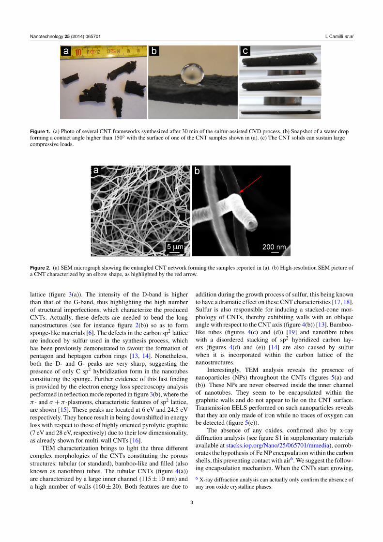
Nanotechnology 25 (2014) 065701 L Camilli et al
Figure 1. (a) Photo of several CNT frameworks synthesized after 30 min of the sulfur-assisted CVD process. (b) Snapshot of a water dropforming a contact angle higher than 150◦ with the surface of one of the CNT samples shown in (a). (c) The CNT solids can sustain largecompressive loads.
Figure 2. (a) SEM micrograph showing the entangled CNT network forming the samples reported in (a). (b) High-resolution SEM picture ofa CNT characterized by an elbow shape, as highlighted by the red arrow.
lattice (figure 3(a)). The intensity of the D-band is higherthan that of the G-band, thus highlighting the high numberof structural imperfections, which characterize the producedCNTs. Actually, these defects are needed to bend the longnanostructures (see for instance figure 2(b)) so as to formsponge-like materials [6]. The defects in the carbon sp2 latticeare induced by sulfur used in the synthesis process, whichhas been previously demonstrated to favour the formation ofpentagon and heptagon carbon rings [13, 14]. Nonetheless,both the D- and G- peaks are very sharp, suggesting thepresence of only C sp2 hybridization form in the nanotubesconstituting the sponge. Further evidence of this last findingis provided by the electron energy loss spectroscopy analysisperformed in reflection mode reported in figure 3(b), where theπ - and σ +π -plasmons, characteristic features of sp2 lattice,are shown [15]. These peaks are located at 6 eV and 24.5 eVrespectively. They hence result in being downshifted in energyloss with respect to those of highly oriented pyrolytic graphite(7 eV and 28 eV, respectively) due to their low dimensionality,as already shown for multi-wall CNTs [16].
TEM characterization brings to light the three differentcomplex morphologies of the CNTs constituting the porousstructures: tubular (or standard), bamboo-like and filled (alsoknown as nanofibre) tubes. The tubular CNTs (figure 4(a))are characterized by a large inner channel (115± 10 nm) anda high number of walls (160± 20). Both features are due to
addition during the growth process of sulfur, this being knownto have a dramatic effect on these CNT characteristics [17, 18].Sulfur is also responsible for inducing a stacked-cone mor-phology of CNTs, thereby exhibiting walls with an obliqueangle with respect to the CNT axis (figure 4(b)) [13]. Bamboo-like tubes (figures 4(c) and (d)) [19] and nanofibre tubeswith a disordered stacking of sp2 hybridized carbon lay-ers (figures 4(d) and (e)) [14] are also caused by sulfurwhen it is incorporated within the carbon lattice of thenanostructures.
Interestingly, TEM analysis reveals the presence ofnanoparticles (NPs) throughout the CNTs (figures 5(a) and(b)). These NPs are never observed inside the inner channelof nanotubes. They seem to be encapsulated within thegraphitic walls and do not appear to lie on the CNT surface.Transmission EELS performed on such nanoparticles revealsthat they are only made of iron while no traces of oxygen canbe detected (figure 5(c)).
The absence of any oxides, confirmed also by x-raydiffraction analysis (see figure S1 in supplementary materialsavailable at stacks.iop.org/Nano/25/065701/mmedia), corrob-orates the hypothesis of Fe NP encapsulation within the carbonshells, this preventing contact with air6. We suggest the follow-ing encapsulation mechanism. When the CNTs start growing,6 X-ray diffraction analysis can actually only confirm the absence ofany iron oxide crystalline phases.
3

Nanotechnology 25 (2014) 065701 L Camilli et al
Figure 3. (a) Raman spectrum of the CNT frameworks. The red andblue curves are the Voigt fit. (b) EELS spectrum in reflection modeacquired with an incident beam of 400 eV.
the numerous structural defects on their surface, induced by thepresence of sulfur, act as preferential sites for immobilizationand subsequent nucleation of Fe atoms coming from ferrocene.The excess of carbon from acetylene gas maintains the growthof carbon layers, which surround and cap the forming Fenuclei. Within this scenario, when the CNTs are exposed toair after the growth process, the carbon shells do not allowany interaction between the particles and the environment soas to prevent their oxidation. It is worth noting that both theCNTs’ inner channel and the external surface are available fordifferential modification or drug loading; this endows themwith potential for targeted therapeutic applications [20].
Figure 6(a) shows the effect of contact time on theabsorption of DCB by the CNT framework. The DCB uptakequickly increases up to about 25% in the first 15 min andthen reaches equilibrium at 46% after 90 min [21]. In orderto highlight the high separation efficiency of the present CNTframework, we collect in the same graph (figure 6(b)) theabsorbed DCB mass in our experiment and that found by Penget al for CNT powders [8], normalized to the initial absorbentmass (i.e. CNTs). It is noteworthy that, in the case of CNTpowders [8], the DCB uptake reaches equilibrium after just40 min, whereas, with our CNT frameworks, the absorptionprocess takes a longer time (90 min). It is our opinion that thisdifference is due to the fact that, owing to the micro-porous
feature of the CNT framework, in our case DCB is not onlyabsorbed onto the CNT surface (like in the case of CNTpowders) but also in the inter-tube space (capillary action).Finally, as a matter of fact, the mass of DCB absorbed withinthe CNT frameworks at equilibrium proves to be about 3.5times higher.
Taking advantage of the oleophilic character of the CNTframework, we employ it as a sponge to efficiently purify waterfrom vegetable and exhaust oil. Owing to its light weightand super-hydrophobicity, the sponge easily floats on thewater surface. Whenever the CNT sponge comes into contactwith the polluted regions, it selectively uptakes the oil film(figure 7). In particular, a 20 mm× 10 mm× 3 mm CNTsponge of 1.5 mg is able to absorb vegetable oil of up to 150times its initial weight, thus exhibiting an absorption capacityhigher than that previously reported for similar 3D carbonmaterials [5]. The absorption capacity is defined as the ratiobetween the final and the initial weight after full absorption.Similarly, our sponge shows an absorption capacity towardsused engine oil slightly higher than that reported by Hashimet al for boron-doped CNT solids [6]. We attribute the superioruptake efficiency of our sample to the presence of (i) highlydefective carbon nanostructures constituting the framework,and (ii) other carbon sp2 species (e.g. nanofibres), beyondthe standard CNTs, characterized by a rough surface (seehigh-resolution SEM micrograph in figure 2(b)). It is indeedknown that using irregular, as opposed to smooth, surfacesmakes the absorption of organics much easier [8].
Once the sponge becomes saturated, the absorbed oil caneasily be removed by squeezing mechanically. Alternatively,igniting the sponge can eliminate the oil, as well. In the lattercase, as soon as all the oil is burnt away, the fire blows outwithout destroying the sponge, which is hence ready to bereused (figure 7(d)). In addition, it is noteworthy to say that,for oil absorption, the sponge can be either dragged by tweezersor driven by a magnet without any direct contact. The presenceof Fe particles inside the CNTs, in fact, confers to the wholeCNT structure a marked magnetic responsiveness at roomtemperature (figure 8). In particular, the measured coerciveforce (Hc) is approximately 340 Oe, a value comparableto that reported in the literature for other Fe-filled CNThybrids [21, 22]. Since the Fe NPs are encapsulated withinthe CNT walls, the burning process does not affect them sothat the magnetic properties of the sponge remain subsequentlyunchanged (figure 8) and the frameworks can be re-driven by amagnet and reused multiple times. This capability to be rapidlyreused makes the CNT frameworks superior to the up-to-datemagnetic polyurethane-based sponges, which need to undergoseveral steps before they recover their initial properties [23].
4. Conclusions
Our results demonstrate that it is possible to obtain a three-dimensional structure entirely made of carbon nanostruc-tures simply by introducing sulfur into a modified ambient-pressure CVD process. Sulfur is needed to manufacture defect-engineered CNTs with curved and bent graphene sheets so asto favour the production of a random and highly interconnected
4

Nanotechnology 25 (2014) 065701 L Camilli et al
Figure 4. (a) TEM image of a tubular (or standard) multi-wall CNT characterized by a large inner channel and a high number of walls.(b) High-resolution TEM micrograph of the CNT in (a), highlighting the oblique angle between the CNT axis and the walls, due to thestacked-cone morphology of the CNT under examination. (c) TEM image of a bamboo-like CNT and (d) its detail. (e) TEM micrograph of ananofibre characterized by a disordered stacking of sp2 hybridized carbon layers. (f) Blow-up of (e).
Figure 5. (a)–(b) Collection of TEM micrographs illustrating the Fe nanoparticles embedded both in filled and in tubular CNTs.(c) Transmission EELS spectrum, showing that the Fe NPs are not oxidized: no trace of O K edge is detected at 530 eV. This spectrum istaken from the particle highlighted by the arrow in (b).
5
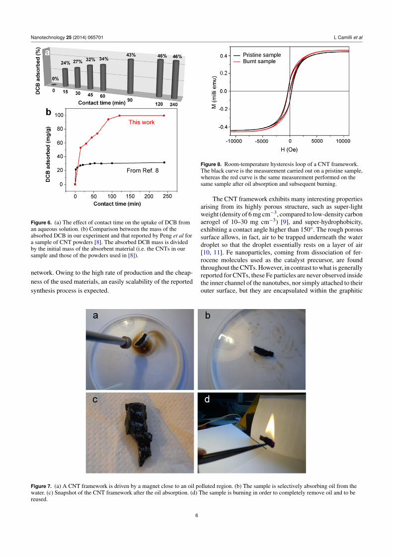
Nanotechnology 25 (2014) 065701 L Camilli et al
Figure 6. (a) The effect of contact time on the uptake of DCB froman aqueous solution. (b) Comparison between the mass of theabsorbed DCB in our experiment and that reported by Peng et al fora sample of CNT powders [8]. The absorbed DCB mass is dividedby the initial mass of the absorbent material (i.e. the CNTs in oursample and those of the powders used in [8]).
network. Owing to the high rate of production and the cheap-ness of the used materials, an easily scalability of the reportedsynthesis process is expected.
Figure 8. Room-temperature hysteresis loop of a CNT framework.The black curve is the measurement carried out on a pristine sample,whereas the red curve is the same measurement performed on thesame sample after oil absorption and subsequent burning.
The CNT framework exhibits many interesting propertiesarising from its highly porous structure, such as super-lightweight (density of 6 mg cm−3, compared to low-density carbonaerogel of 10–30 mg cm−3) [9], and super-hydrophobicity,exhibiting a contact angle higher than 150◦. The rough poroussurface allows, in fact, air to be trapped underneath the waterdroplet so that the droplet essentially rests on a layer of air[10, 11]. Fe nanoparticles, coming from dissociation of fer-rocene molecules used as the catalyst precursor, are foundthroughout the CNTs. However, in contrast to what is generallyreported for CNTs, these Fe particles are never observed insidethe inner channel of the nanotubes, nor simply attached to theirouter surface, but they are encapsulated within the graphitic
Figure 7. (a) A CNT framework is driven by a magnet close to an oil polluted region. (b) The sample is selectively absorbing oil from thewater. (c) Snapshot of the CNT framework after the oil absorption. (d) The sample is burning in order to completely remove oil and to bereused.
6

Nanotechnology 25 (2014) 065701 L Camilli et al
walls. This means that both the CNTs’ inner channel and theexternal surface are available for differential modification ordrug loading. Similar samples of graphite-coated nanomag-nets have been demonstrated to be promising candidates forminimally invasive targeted drug delivery platforms [24].
By taking advantage of its hydrophobic and oleophilicproperties as well as its micro-porous features, we show thatthis carbon framework may be an ideal candidate for use asan absorbent for oil/water separation and the removal of toxicorganic solvents (i.e. o-dichlorobenzene) from water. Notably,our sample exhibits an oil-absorption capacity higher than thatreported in the literature for similar CNT sponges [5, 6]. Thisfinding is due to the presence, in our sample, of highly defectivenanostructures characterized by a rough surface that facilitatesthe absorption process. In addition, once the sponges becomesaturated with oil/chemicals, the absorbed material can easilybe removed either by mechanical squeezing or by igniting thesponge. Therefore, they can be recycled several times.
Our findings enable us to predict that the reported carbonframeworks, due to the volume of the shown properties,will be useful for practical applications in filtration andwater treatment, as well as for soft magnetic memories andmagnetic targeted drug delivery platforms. Finally, a thoroughinvestigation of the toxicity of CNT sponges is undoubtedlyrequired, particularly after the discovery that long CNTs maybe more harmful than short ones [25].
Acknowledgments
We acknowledge the financial support of the European Officeof Aerospace Research and Development (EOARD) throughthe Air Force Office of Scientific Research Material Command,USAF, under Grant No. FA8655-11-1-3036.
References
[1] Roberge F, Gravel M J, Deschenes L, Guy C and Samson R2001 Biofiltration of dichlorobenzene Water Sci. Technol.44 287
[2] Hill G A, Tomusiak M E, Quail B and Cleave K M V 1991Bioreactor design effects on biodegradation capabilities ofVOCs in wastewater Environ. Prog. 10 147
[3] Upadhyayula V K K, Ruparelia J P and Agrawal A 2011 Useof carbon nanotubes in water treatment NanoscaleMultifunctional Materials: Science and Applications edS M Mukhopadhyay (Hoboken, NJ: Wiley) pp 321–68
[4] Upadhyayula V K K, Deng S, Mitchell M C and Smith G B2009 Application of carbon nanotube technology forremoval of contaminants in drinking water: a review Sci.Tot. Environ. 408 1
[5] Gui X, Wei J, Wang K, Cao A, Zhu H, Jia Y, Shu Q and Wu D2010 Carbon nanotube sponges Adv. Mater. 22 617
[6] Hashim D P et al 2012 Covalently bonded three-dimensionalcarbon nanotube solids via boron induced nanojunction Sci.Rep. 2 363
[7] Tibbets G G, Bernard C A and Gorkiewicz D W 1994 Role ofsulfur in the production of carbon fibers in the vapor phaseCarbon 32 569
[8] Peng X, Li Y, Luan Z, Di Z, Wang H, Tian B and Jia Z 2003Adsorption of 1,2-dichlorobenzene from water to carbonnanotubes Chem. Phys. Lett. 376 154
[9] Bryning M B, Milkie D E, Islam M F, Hough L A,Kikkawa J M and Yodh A G 2007 Carbon nanotubeaerogels Adv. Mater. 19 661
[10] Wenzel R N 1936 Resistance of solid surface to wetting bywater Indust. Eng. Chem. 28 988
[11] Cassie A B D and Baxter S 1944 Wettability of poroussurfaces Trans. Faraday Soc. 40 546
[12] Camilli L, Pisani C, Passacantando M, Grossi V, Scarselli M,Castrucci P and De Crescenzi M 2013 Pressure-dependentelectrical conductivity of freestanding three-dimensionalcarbon nanotube network Appl. Phys. Lett. 102 183117
[13] Romo-Herrera J M, Sumpter B G, Cullen D A, Terrones H,Cruz-Silva E, Smith D J, Meunier V and Terrones M 2008An atomistic branching mechanism for carbon nanotubes:sulfur as the triggering agent Angew. Chem. Int. Edn 472948
[14] Romo-Herrera J M, Cullen D A, Cruz-Silva E, Ramirez D,Sumpter B G, Meunier V, Terrones H, Smith D J andTerrones M 2009 The role of sulfur in the synthesis of novelcarbon morphologies: from covalent Y-junctions tosea-urchin-like structures Adv. Funct. Mater. 19 1193
[15] Calliari L, Fanchenko S and Filippi M 2007 Plasmon featuresin electron energy loss spectra from carbon materialsCarbon 45 1410
[16] Castrucci P, Scilletta C, Del Gobbo S, Scarselli M, Camilli L,Simeoni M, Belley D, Continenza A and De Crescenzi M2011 Light harvesting with multiwall carbonnanotube/silicon heterojunctions Nanotechnology22 115701
[17] Wei J et al 2007 The effect of sulfur on the number of layers ina carbon nanotube Carbon 45 2152
[18] Ren W, Li F, Bai S and Cheng H M 2006 The effect of sulfuron the structure of carbon nanotubes produced by a floatingcatalyst method J. Nanosci. Nanotechnol. 6 1339
[19] Cui T, Lv R, Huang Z H, Kang F, Wang K and Wu D 2011Effect of sulfur on enhancing nitrogen-doping and magneticproperties of carbon nanotubes Nanoscale Res. Lett. 6 77
[20] Vermisoglou E C, Pilatos G, Romanos G E, Devlin E,Kanellopoulos N K and Karanikolos G N 2011 Magneticcarbon nanotubes with particle-free surfaces and high drugloading capacity Nanotechnology 2 355602
[21] Gui X, Wei J, Wang K, Wang W, Lv R, Chang J, Kang F, Gu Jand Wu D 2008 Improved filling rate and enhancedmagnetic properties of Fe-filled carbon nanotubes byannealing and magnetic separation Mater. Res. Bull.43 3441
[22] Camilli L et al 2012 High coercivity of iron filled carbonnanotubes synthesized on austenitic stainless steel Carbon50 718
[23] Calcagnile P, Fragouli D, Bayer I S, Anyfantis G C,Martiradonna L, Cozzoli P D, Cingolani R andAthanassiou A 2012 Magnetically driven floating foams forthe removal of oil contaminants from water ACS Nano 65413
[24] Zeeshan M A et al 2013 Graphite coating of iron nanowiresfor nanorobotic applications: synthesis, characterization andmagnetic wireless manipulation Adv. Funct. Mater. 23 823
[25] Ali-Boucetta H et al 2013 Asbestos-like pathogenicity of longcarbon nanotubes alleviated by chemical functionalizationAngew. Chem. Int. Edn 62 2274
7

Formation of a protected sub-band for conductionin quantum point contacts under extreme biasingJ. Lee1, J. E. Han2*, S. Xiao1, J. Song1, J. L. Reno3 and J. P. Bird1*
Managing energy dissipation is critical to the scaling of currentmicroelectronics1–3 and to the development of novel devicesthat use quantum coherence to achieve enhanced functional-ity4. To this end, strategies are needed to tailor the electron–phonon interaction, which is the dominant mechanism forcooling non-equilibrium (‘hot’) carriers5,6. In experimentsaimed at controlling the quantum state7–11, this interactioncauses decoherence that fundamentally disrupts device oper-ation12,13. Here, we show a contrasting behaviour, in whichstrong electron–phonon scattering can instead be used to gen-erate a robust mode for electrical conduction in GaAs quantumpoint contacts, driven into extreme non-equilibrium by nanose-cond voltage pulses. When the amplitude of these pulses ismuch larger than all other relevant energy scales, strong elec-tron–phonon scattering induces an attraction between elec-trons in the quantum-point-contact channel, which leads tothe spontaneous formation of a narrow current filament andto a renormalization of the electronic states responsible fortransport. The lowest of these states coalesce to form a sub-band separated from all others by an energy gap larger thanthe source voltage. Evidence for this renormalization is pro-vided by a suppression of heating-related signatures in thetransient conductance, which becomes pinned near 2e2/h (e,electron charge; h, Planck constant) for a broad range ofsource and gate voltages. This collective non-equilibriummode is observed over a wide range of temperature(4.2–300 K) and may provide an effective means to manageelectron–phonon scattering in nanoscale devices.
Transient heating of carriers is investigated in quantum pointcontacts (QPCs)14–16 implemented in the high-mobility two-dimen-sional electron gas (2DEG) of a GaAs/AlGaAs heterostructure. Thedevices are formed by applying a voltage Vg to a pair of split-metalgates (Fig. 1a), thereby allowing electrons to be efficiently confinedto a nanoscale channel within their gap. Such strong confinementquantizes electron motion to form a set of quasi-one-dimensional(1D) sub-bands with an equilibrium separation D on the order ofa few meV (refs 13,16). There have been many studies of non-equi-librium transport in QPCs under conditions where the source biasVsd used to drive current through them is comparable to D(ref. 16). In contrast, the new physics we discuss here is obtainedin the extreme non-equilibrium limit, where the bias is verymuch larger than all other energy scales in the system (that is,eVsd ≈ 100 mV ≫ D and EF, where EF is the Fermi energy in the2DEG and is measured relative to the conduction-band edge).
To perform a real-time probe of electron–phonon energyexchange we carried out transient electrical measurements17,18 (seeMethods). These studies were performed at 4.2 K on three QPCs(A, B and C; see Methods) that exhibited quantitatively similar be-haviour. Figure 1b presents the typical transient response obtained
in such an experiment. Here, a voltage pulse of fixed amplitude(Vp, in this case 150 mV, dotted line) was applied to the sourcereservoir of the QPC and the current flowing through it wasmeasured by connecting its drain to the 50 V input of a fast oscillo-scope. The transient output plotted in Fig. 1b is actually the voltageat this input, and is therefore directly proportional to the QPCcurrent (and conductance, I/V). The results of Fig. 1b were obtainedfor several ranges of Vg, spanning the regimes identified relative tothe QPC linear conductance Gl in Fig. 1c (note that, due to thermalsmearing of the 1D sub-bands, no quantization is evident in thisfigure19). In the 2D regime, the gate voltage is insufficient todefine the QPC and the form of the output pulse closely resemblesthat of the input. As the QPC forms, however, one first enters themultimode 1D regime where the output voltage shows a pro-nounced increase over many nanoseconds, even though the inputhas already reached its maximum. Because the 150 mV pulse inFig. 1b is much larger than the GaAs longitudinal-optical (LO)phonon energy of hvLO ≈ 36 meV (h¼ h/2p; vLO, LO-phononfrequency), we attribute this behaviour to heating that arises whenhot electrons injected into the QPC rapidly lose energy throughoptical-phonon emission (Fig. 2b, lower inset)20–23. The emittedphonons in turn quickly decay into acoustic modes, which thenconduct heat back from the drain to the source, raising the electrontemperature on this side of the device. As the source electrons areheated, their thermionic emission over the QPC barrier increases,leading to the time-dependent increase of current seen in the multi-mode 1D regime. Several points may be made regarding this feed-back process, the first of which is that, because of the large energybarrier blocking their reinjection back to the source (see the lowerinset in Fig. 2b), thermalized electrons in the drain cannot contrib-ute to this heat flow. Indeed, such reinjection would cause a decreaseof current over time24, behaviour completely opposite to theobserved transient response. The second point is that althoughinjected carriers experience lateral confinement as they passthrough the QPC, the generated phonons themselves are uncon-fined and propagate in bulk GaAs. Finally, we note that the charac-teristic timescale associated with the heating (�10 ns) should belimited by that required for phonon diffusion from the drain tothe source. Taking an associated distance of �1 mm, we infer aphonon diffusivity of 1 cm2s21. Given the uncertainty in the sizeof the effective region that is relevant for heat transfer, this valueappears consistent with previous measurements of the thermal dif-fusivity of GaAs25 and with the non-equilibrium nature of thephonon population generated under these conditions (see the dis-cussion regarding ref. 1 in the Supplementary Information).
A notable change occurs on entering the few-mode 1D regime,where the output voltage quickly rises to become constant overthe full width of the pulse (Fig. 1b), indicating that heating is nolonger effective in assisting transport. One possibility is that this
1Department of Electrical Engineering, University at Buffalo, State University of New York, 230 Davis Hall, Buffalo, New York 14260-1900, USA,2Department of Physics, University at Buffalo, State University of New York, 239 Fronczak Hall, Buffalo, New York 14260-1500, USA, 3CINT, Sandia NationalLaboratories, Department 1131, MS 1303, Albuquerque, New Mexico 87185, USA. *e-mail: [email protected]; [email protected]
LETTERSPUBLISHED ONLINE: 19 JANUARY 2014 | DOI: 10.1038/NNANO.2013.297
NATURE NANOTECHNOLOGY | ADVANCE ONLINE PUBLICATION | www.nature.com/naturenanotechnology 1
© 2014 Macmillan Publishers Limited. All rights reserved.

change in transient response arises as the current through the QPCis reduced below some threshold, leading to a similar decrease in thephonon emission responsible for the heating. Our investigationsindicate, however, that this is not the case. Figure 1d compares tran-sient curves obtained by applying 100 and 400 mV input pulses tothe device. Although no signs of heating are evident for the400 mV input, the 100 mV data show a clear, heating-relatedincrease over time, even though the overall current level is lowerthan for the 400 mV pulse. Such different responses are inconsistentwith the existence of a threshold current for the onset of heating. Infact, by analysing the dependence of the output-pulse time constant(t, defined as the 10–90% rise time of the output pulse, see upperinset of Fig. 2b), we find that the quenching instead occurs as theQPC undergoes a transition to single-sub-band transport. This isdemonstrated in Fig. 2a, where we plot the dependence of t on tran-sient conductance (determined from the QPC current and voltage atthe end of the pulse). Results for pulses of various amplitude areplotted and all follow a common variation. As the conductancedecreases from its maximum at Vg¼ 0 (2D regime), t grows steadilyas the QPC forms and heating starts. As the conductance isdecreased below 3 × 2e2/h, however, we find that t drops very sud-denly, indicating that the abovementioned heating is no longereffective at increasing the current.
Accompanying the quenching of heating in the few-moderegime, we find the transient conductance becomes insensitive tolarge variations in the pulse amplitude, even though these wouldnormally be expected to strongly affect the conductance by changingthe number of sub-bands involved in transport16. This is illustratedin Fig. 2b, which shows the gate-voltage-dependent variation of thetransient conductance, determined using input pulses in the range50–400 mV. From this graph we identify two distinct regimes of be-haviour. For Vg . 20.5 V, which encompasses the 2D and multi-mode 1D regimes, the transient conductance depends strongly onpulse amplitude, much as would normally be expected. (Relativeto the natural level spacing of the QPC, the pulse amplitudes usedin our experiments lie in the range 10–100D/e.) For Vg , 20.5 V,however, one enters the few-mode 1D regime (see Fig. 2a and itsinset). Here, we see that the various curves collapse onto acommon variation, independent of pulse amplitude. A furtheraspect of this regime is apparent in Fig. 3a, where we plot the transientconductance as a function of Gl. Data are presented for all three QPCsand clearly demonstrate that the transient conductance becomespinned near 2e2/h, taking a value of 0.5 × 2e2/h–1 × 2e2/h for awide range of Gl (that is, gate voltage) and pulse amplitude.
The implication of our experiment is that transport changes sig-nificantly when carriers are driven far from equilibrium, while
300 nm
Pulse-generator: Vp
50 ΩMatching
resistor(on-chip)
50 Ω inputof digital samplingoscilloscope
10−2
10−1
100
101
102
20
10
Gate voltage (V)
−1.2 −0.8
GI (2e2/h)
−0.4 0.0 30 50 70 90
Time (ns)
0
2
1
0
2
3
1
0
0.004
0.012
0.016
40 60Time (ns)
V out (
V)
Vout
Vg
Vg
Vout (m
V)
V out (
mV
)
80
2D regime
Multimode1D regime
Few-mode1D regime
b S D
a
2D regime
Multimode1D regime
Few-mode1D regime
c d
8.0 kΩ
2.2 kΩ
Figure 1 | Transient response of QPC-C. a, Schematic of the pulsed-measurement set-up. Transient voltage Vp is applied to the QPC source S through a
coaxial cable with on-chip 50 V termination to provide full impedance matching. The current flowing to drain D is then determined by measuring the voltage
Vout that develops across the 50 V input of a digital sampling oscilloscope. This latter 50 V impedance is therefore in series with the QPC resistance. Further
details on the transient measurements are given in the Methods. The colourized image shows a close-up view of the QPC gates (green) on the top surface
(purple) of the GaAs/AlGaAs heterojunction. When biased with an appropriate voltage (Vg, biasing scheme shown), a tunable depletion region develops
around the gates, the extent of which is represented schematically by the pair of white dotted lines. b, Form of the input pulse (Vp, dotted line) and the
output pulse for several different ranges of gate voltage. Input pulse Vp¼ 150 mV is plotted, scaled by a factor of 1/10. In the 2D regime, the output pulses
are obtained for Vg¼0, 21 and 22 mV and are scaled by a factor of 1/5. For the upper and lower set of curves in the multimode 1D regime, the gate
voltage is incremented in 1 mV steps over the range 20.554 V ≤ Vg ≤ 20.550 V and 20.604 V ≤ Vg ≤ 20.600 V, respectively. In the few-mode 1D regime,
the gate voltage is incremented in 1 mV steps over the range 20.800 V ≤ Vg ≤ 20.796 V. c, Variation of the linear conductance of the QPC as a function
of gate voltage. Different transport regimes are identified. d, Comparison of transient pulses for different input pulses and gate conditions. Upper pulse:
Vg¼20.74 V and Vp¼ 400 mV. Lower pulse: Vg¼20.62 V and Vp¼ 100 mV. For each measurement we indicate the steady-state resistance reached near
the end of the pulse.
LETTERS NATURE NANOTECHNOLOGY DOI: 10.1038/NNANO.2013.297
NATURE NANOTECHNOLOGY | ADVANCE ONLINE PUBLICATION | www.nature.com/naturenanotechnology2
© 2014 Macmillan Publishers Limited. All rights reserved.

simultaneously being subjected to strong lateral confinement.Under such conditions, the conductance appears to be dominatedby a single ‘protected’ sub-band that shows unexpected immunityto local heating and large variations in Vp. To account for this be-haviour theoretically, we recall that it occurs in a regime where
the transient current becomes independent of time. This indicatesthat the protected sub-band is associated with a new steady state,one that is established on a timescale much faster than that of ourexperiment. To describe this steady state, we calculate the effectiveinter-sub-band coupling arising from electron–phonon scattering.
a
b
10−1
100
101
102
Gate voltage (V)−1.0 0.0
1,0001001010
5
10
15
20
25
0.2−0.4−0.6−0.8
10%
90% 100% 0.012
0.003
020 70
Time (ns)
V out (
V)
τ
Con
duct
ance
(2e2 /
h)
μs
μd
1
2
3
Transient conductance (2e2/h)
τ (ns
)
τ (ns
)
20
10
0−1 0Gate voltage (V)
Figure 2 | Different regimes of nonlinear transport and their manifestation
in the conductance. a, Main panel: Variation in output-pulse time constant t
as a function of transient conductance for QPC-C with several different
input-pulse amplitudes (red, Vp¼ 50 mV; dark blue, Vp¼ 100 mV; green,
Vp¼ 200 mV; light blue, Vp¼ 400 mV). Grey shading indicates the range of
conductance over which the time constant drops significantly as the few-
mode 1D regime is entered. Inset: Same variation of t, but as a function of
Vg. b, Main panel: Variation of transient conductance of QPC-C with Vg for
several different input pulses (red, Vp¼ 50 mV; dark blue, Vp¼ 100 mV;
purple, Vp¼ 150 mV; green, Vp¼ 200 mV; orange, Vp¼ 300 mV; light blue,
Vp¼ 400 mV). Three error bars are included for the 50 mV data (those
with the largest error) to indicate their uncertainty. These error bars were
determined using the peak-to-peak noise in the output pulses to determine
a corresponding spread in the calculated value of the transient conductance.
Lower inset: Schematic of the QPC under bias. Red line: Variation of the
conduction-band edge along the length of the QPC under strong biasing.
Black wavy lines: Optical phonons emitted by injected hot carriers. (1) Hot
electrons are injected into the QPC. (2) These electrons rapidly lose energy
by optical-phonon emission. (3) Heat is conducted back to the source by
acoustic phonons. ms and md are the quasi-Fermi levels in the source and
drain, respectively, the grey shading indicates the region where there is
strong lateral confinement in the QPC. Upper inset: The value of t is
determined experimentally from the 10–90% rise time of the output pulse.
a
b
V(y)
y
c
y (in units of ℓ)
y = 0
y = 0
eVsd = 0 eVsd Δ, EF, ħωLO
ρ(y)
ħωLO
15
10
5
0
Vsd (mV)
Sub-
band
bot
tom
(meV
)
2−2
2020
10−4 10−3 10−2 10−110−1
100
101
100 101
0
−50
−100
−150
−200
40
Linear conductance (2e2/h)
Tran
sien
t con
duct
ance
(2e2 /
h)
60 80 100
Figure 3 | Sub-band renormalization under high bias. a, Variation of
transient conductance as a function of linear conductance, measured in
QPCs A (open circles), B (filled triangles) and C (filled circles). The colour
of the various symbols indicates the input-pulse amplitude (green,
Vp¼ 50 mV; light blue, Vp¼ 100 mV; dark blue, Vp¼ 150 mV; purple,
Vp¼ 200 mV; red, Vp¼ 300 mV; black, Vp¼ 400 mV). The horizontal
dotted line denotes a conductance value of 2e2/h. Inset: Modification of the
transverse component of the confining potential V(y) under application of a
large bias. Shown at the left is the form of the potential at zero bias. As
indicated on the right, which corresponds to the case for which sub-band
renormalization is well established, strong electron–phonon coupling causes
the potential to develop a deep minimum under application of large bias.
b, Calculated sub-band bottom for the ten lowest sub-bands as a function of
Vsd. The black line corresponds to the lowest sub-band and the sub-band
index increases systematically from 1 to 10 on moving upwards from the
lowest curve. The vertical dotted line indicates the optical-phonon energy,
and the red dashed line denotes the electrochemical potential (as measured
from the edge of the lowest sub-band). Error bars represent level
broadening due to dephasing introduced by the inter-sub-band transitions.
c, Electron density in the transverse direction, calculated at several
different values of Vsd (red, Vsd¼ 4 mV; green, Vsd¼ 20 mV; dark blue,
Vsd¼ 24 mV; black, Vsd¼ 30 mV; light blue, Vsd¼ 60 mV). The transverse
position is plotted in units of the characteristic length of the original
harmonic potential, ℓ =���������h2/m∗D
√≈ 32 nm for D¼ 1 meV, where m∗ is the
electron effective mass for a 2DEG in GaAs. (Supplementary Section 1).
NATURE NANOTECHNOLOGY DOI: 10.1038/NNANO.2013.297 LETTERS
NATURE NANOTECHNOLOGY | ADVANCE ONLINE PUBLICATION | www.nature.com/naturenanotechnology 3
© 2014 Macmillan Publishers Limited. All rights reserved.

In doing so, we treat the electron–phonon interaction in secondorder, including contributions from Hartree- and exchange-liketerms that mediate an effective attraction between electrons(similar to discussions of superconductivity). Our model accountsfor the quasi-1D nature of the electronic states in the QPC andfor their interaction with bulk GaAs phonons. A key assumption,driven by the phenomenology of the experiment, is that electron–phonon coupling under extreme non-equilibrium is strongly depen-dent on the local electron density, a characteristic that we incorpor-ate empirically by imposing (Supplementary Section 1) a nonlinearcorrection to this coupling. This correction gives rise to positivefeedback, in which the phonon-mediated attraction induces alocal enhancement of the electron density, producing an even stron-ger attraction. As this feedback grows with increasing Vsd, a self-organized spatial inhomogeneity, consisting of a narrow currentfilament that flows along the centre line of the QPC, ultimatelydevelops spontaneously. (Although we use the notation Vsd andVp interchangeably, the reader is referred to the comment on thispoint in the Methods.) The filament is confined to a narrow dipin the transverse potential, the width of which is much narrowerthan that of the QPC (see schematics in the inset to Fig. 3a). Thisextreme collimation26,27 is responsible, in turn, for a renormalizationof the sub-band spectrum, the ground state of which is bound in thenarrow well and corresponds to the protected sub-band.
To provide quantitative support for the statements above, inFig. 3b we plot the variation of the self-consistently computedsub-band edges as a function of Vsd (the zero of energy in thisfigure is taken to correspond to the edge of the lowest sub-band atzero bias). Beyond a certain threshold (Vsd ≈ 20 mV for the set ofparameters considered here), the lowest sub-band splits away fromthe others by an amount that quickly exceeds the bias voltageitself. The dashed line in the figure represents the correspondingvariation of the electrochemical potential, which is separated fromthe ground-state energy by eVsd. From the position of this potential,and that of the renormalized levels, we see that only the ground sub-band should have any significant occupation. Higher ones, in con-trast, being tens of meV above the electrochemical potential,should only be weakly occupied and so contribute little to the con-ductance. A concern here might be dephasing introduced by theinter-sub-band transitions, so we have also determined the levelbroadening due to this (Supplementary Section 1). We find thatthis broadening increases significantly once the bias exceeds theLO-phonon energy (see the vertical bars in Fig. 3b), but it nonethe-less remains smaller than the principal sub-band gap at all values ofVsd. Indeed, an argument in Supplementary Section 1 indicates thatthe sub-band gap ultimately scales as Vsd, while the broadening onlyincreases as V sd
0.5. From these observations we therefore concludethat the lowest sub-band should dominate transport.
Formation of the narrow current filament associated with theprotected sub-band is shown in Fig. 3c. Here, we plot the chargedensity for this sub-band at several bias voltages, while in theinset of Fig. 3a we depict its contribution to the self-consistent trans-verse potential of the QPC. Although the density is initially (atVsd¼ 0) spread across the full width of the QPC, with increasingVsd it becomes strongly localized near the channel centre. Themanner in which this occurs is highly nonlinear in Vsd, with theonset occurring suddenly when Vsd reaches the range of bias(Vsd ≈ 20–24 mV) at which the protected sub-band begins to splitaway from the higher ones. The maximum conductance of the pro-tected sub-band will be 2e2/h, but its specific value will be reducedby carrier scattering beyond our model, or by a situation in whichthe applied voltage is not fully dropped within the range of the sub-band16. Such considerations should account for the observed‘pinning’ of the transient conductance near, but below, 2e2/h in Fig. 3a.
Thus far, we have discussed the transient response at 4.2 K,where the thermal energy is some two orders of magnitude
smaller the scale of the sub-band renormalization. The renormaliza-tion is robust to significant changes in temperature, however, as wedemonstrate in Supplementary Section 2 for measurements made atroom temperature. Indeed, because the energy transfer processesindicated in the lower inset to Fig. 2b are quite generic to semicon-ductor devices, our observations provide an important demon-stration of how hot-carrier relaxation via strong phonon emissionmay be managed in nanodevices. These may include nanoscaledtransistors, which have a band profile under strong bias that stronglyresembles that considered here, or other quasi-1D conductors suchas carbon nanotubes and graphene nanoribbons. At a more funda-mental level, it has long been known that non-trivial collective stateswill form to effectively avoid dominant interactions28–30. The trans-port mechanism we report provides a novel manifestation of thisprinciple, with protection from residual inelastic electron–phononbackscattering arising when the electronic wavefunction self-organizes into a coherent (transverse) bound state under high bias.
MethodsDevice fabrication. The three QPCs studied here were fabricated separately in thesame high-mobility GaAs/AlGaAs heterostructure (Sandia sample VA0284).The 2DEG in these devices had a density of �2.5 × 1011 cm22 and a mobility near1.5 × 106 cm2 V21 s21, with a corresponding mean free path . 11 mm (all at 4.2 K).The QPCs were fabricated with the same gate pattern (Fig. 1a) and differed onlyin the size of their two-terminal mesa (length × width ¼ 60 mm × 470 mm,180 mm × 160 mm and 900 mm × 470 mm in QPCs A, B and C, respectively).However, the effects reported here were not dependent on mesa size.
Transient-measurement techniques. Transient conductance was measured bybonding the QPCs into a high-speed chip carrier and using 50 V matchedtransmission lines to source and sink voltage pulses. A 50 V thick film resistor,mounted directly on the chip carrier, provided termination of the input signal toground (Fig. 1a). Pulsing was performed using an AVTECH generator to sourcepulses with rise times as short as 200 ps, at a repetition frequency of 1 MHz. TheQPC transient current could then be determined from the voltage (Vout) measured atthe 50 V input of a Tektronix digital sampling oscilloscope (50 GHz bandwidth).The applied transient voltage Vp was therefore dropped across the seriescombination of the QPC and this 50 V impedance, although in the regime of interestthe QPC resistance was larger than 10 kV and its source–drain voltage was thereforeessentially equal to Vp. The chip carrier was mounted at the cold end of a custom-built insert31 that was cooled to 4.2 K in a vacuum can. Helium exchange gas wasused to provide thermal connection to a liquid-helium bath. The d.c. electricalcharacteristics could also be measured with this set-up by using a Keithley 2400source meter to determine the I–V curves as a function of Vsd and Vg. Numericaldifferentiation of these curves was then performed to obtain the d.c.differential conductance.
Theoretical model. We consider a model of a 1D wire, with free motion along thex-direction and a harmonic confining potential in the transverse ( y-) direction(where the channel centre corresponds to y¼ 0). The Hamiltonian describingthe electron–phonon interaction is written as
H =∫∑
ns
c†ns x( ) nD− h2
2m∂2
∂x2
( )cns x( ) dx
+∑
nmsa
Manmwac†ns xa( )
cms xa( )
+∑a
12
w2a + v2
LOw2a
( ) (1)
where a local LO phonon wa of frequency vLO, located at position (xa , ya), mediatesan effective coupling between states of the nth and mth sub-bands. c†/c arecreation/annihilation operators, while s denotes the spin (taken here to be degenerate).The coupling matrix element (Manm) appearing in equation (1) is modelled as
Manm = g(ya) ·�����vLO
2h
√fn ya( )
fm ya( )
with g y( )[ ]2= g2
0 1 + lℓ2r y( )[ ]
(2)
where fn( y) is the harmonic-oscillator function for the nth sub-band, ℓ is acharacteristic confinement length, r( y) is the local electron density, and theparameters g0 and l govern the strength and nonlinearity of the electron–phononinteraction. Further details on the definition of these parameters can be found inSupplementary Section 1, where we present our full theoretical treatment ofthis problem.
Received 26 March 2013; accepted 5 December 2013;published online 19 January 2014
LETTERS NATURE NANOTECHNOLOGY DOI: 10.1038/NNANO.2013.297
NATURE NANOTECHNOLOGY | ADVANCE ONLINE PUBLICATION | www.nature.com/naturenanotechnology4
© 2014 Macmillan Publishers Limited. All rights reserved.

References1. Chau, R., Doyle, B., Datta, S., Kavalieros, J. & Zhang, K. Integrated
nanoelectronics for the future. Nature Mater. 6, 810–812 (2007).2. Pop, E. Energy dissipation and transport in nanoscale devices. Nano. Res. 3,
147–169 (2010).3. Chang, L. et al. Practical strategies for power-efficient computing technologies.
Proc. IEEE 98, 215–236 (2010).4. Awschalom, D. D., Bassett, L. C., Dzurak, A. S., Hu, E. L. & Petta, J. R. Quantum
spintronics: engineering and manipulating atom-like spins in semiconductors.Science 339, 1174–1179 (2013).
5. Ferry, D. K. Semiconductor Transport (Taylor & Francis, 2001).6. Lundstrom, M. Fundamentals of Carrier Transport (Cambridge Univ.
Press, 2009).7. Khrapai, V. S., Ludwig, S., Kotthaus, J. P., Tranitz, H. P. & Wegscheider, W.
Double-dot quantum ratchet driven by an independently biased quantum pointcontact. Phys. Rev. Lett. 97, 176803 (2006).
8. Schinner, G. J., Tranitz, H. P., Wegscheider, W., Kotthaus, J. P. & Ludwig, S.Phonon-mediated nonequilibrium interaction between nanoscale devices. Phys.Rev. Lett. 102, 186801 (2009).
9. Gasser, U. et al. Statistical electron excitation in a double quantum dot inducedby two independent quantum point contacts. Phys. Rev. B 79, 035303 (2009).
10. Harbusch, D., Taubert, D., Tranitz, H. P., Wegscheider, W. & Ludwig, S.Phonon-mediated versus Coulombic backaction in quantum dot circuits. Phys.Rev. Lett. 104, 196801 (2010).
11. Granger, G. et al. Quantum interference and phonon-mediated backaction inlateral quantum-dot circuits. Nature Phys. 8, 522–527 (2012).
12. Lin, J. J. & Bird, J. P. Recent experimental studies of electron dephasing in metaland semiconductor mesoscopic structures. J. Phys. 14, R501–R596 (2002).
13. Ferry, D. K., Goodnick, S. M. & Bird, J. P. Transport in Nanostructures(Cambridge Univ. Press, 2009).
14. Van Wees, B. J. et al. Quantized conductance of point contacts in atwo-dimensional electron gas. Phys. Rev. Lett. 60, 848–850 (1988).
15. Wharam, D. A. et al. One-dimensional transport and the quantization of theballistic resistance. J. Phys. C 21, L209–L214 (1988).
16. Micolich, A. P. What lurks below the last plateau: experimental studies of the0.7 × 2e2/h conductance anomaly in one-dimensional systems. J. Phys. 23,443201 (2011).
17. Zhitenev, N. B, Haug, R. J., v. Klitzing, K. & Eberl, K. Time-resolvedmeasurements of transport in edge channels. Phys. Rev. Lett. 71,2292–2295 (1993).
18. Zhitenev, N. B., Haug, R. J., v. Klitzing, K. & Eberl, K. Linear and nonlinearwaves in edge channels. Phys. Rev. B 52, 11277–11283 (1995).
19. Van Wees, B. J. et al. Quantum ballistic and adiabatic electron transport studiedwith quantum point contacts. Phys. Rev. B 43, 12431–12453 (1991).
20. Heiblum, M., Nathan, M. I., Thomas, D. C. & Knoedler, C. M. Directobservation of ballistic transport in GaAs. Phys. Rev. Lett. 55, 2200–2203 (1985).
21. Heiblum, M., Galbi, D. & Weckwerth, M. Observation of single-optical-phononemission. Phys. Rev. Lett. 62, 1057–1060 (1989).
22. Sivan, U., Heiblum, M. & Umbach, C. P. Hot ballistic transport and phononemission in a two-dimensional electron gas. Phys. Rev. Lett. 63, 992–995 (1989).
23. Dzurak, A. S. et al. Two-dimensional electron-gas heating and phonon emissionby hot ballistic electrons. Phys. Rev. B 45, 6309–6312 (1992).
24. Datta, S., Assad, F. & Lundstrom, M. S. The silicon MOSFET from atransmission viewpoint. Superlatt. Microstruct. 23, 771–780 (1998).
25. Soltanolkotabi, M., Bennis, G. L. & Gupta, R. Temperature dependence of thethermal diffusivity of GaAs in the 100–305 K range measured by the pulsedphotothermal displacement technique. J. Appl. Phys. 85, 794–798 (1999).
26. Beenakker, C. W. J. & van Houten, H. in Solid State Physics (eds Ehrenreich, H. &Turnbull, D.) Vol. 44, 1–228 (Academic, 1991).
27. Topinka, M. A. et al. Imaging coherent electron flow from a quantum pointcontact. Science 289, 2323–2326 (2000).
28. Anderson, P. W. More is different. Science 177, 393–396 (1972).29. Glazman, L. I., Hekking, F. W. J. & Larkin, A. L. Spin-charge separation and the
Kondo effect in an open quantum dot. Phys. Rev. Lett. 83, 1830–1833 (1999).30. Pines, D. & Bohm, D. A collective description of electron interactions: II.
Collective vs. individual particle aspects of the interactions. Phys. Rev. 85,338–353 (1952).
31. Naser, B. et al. 50-Ohm-matched system for low-temperature measurements ofthe time-resolved conductance of low-dimensional semiconductors. Rev. Sci.Instrum. 76, 113905 (2005)
AcknowledgementsThis research was supported by the US Department of Energy, Office of Basic EnergySciences, Division of Materials Sciences and Engineering (award DE-FG02-04ER46180).The work was performed, in part, at the Center for Integrated Nanotechnologies, a USDepartment of Energy, Office of Basic Energy Sciences user facility. Sandia NationalLaboratories is a multi-program laboratory managed and operated by Sandia Corporation,a wholly owned subsidiary of Lockheed Martin Corporation, for the US Department ofEnergy’s National Nuclear Security Administration (contract DE-AC04-94AL85000).J.E.H. acknowledges support from the National Science Foundation (DMR-0907150).
Author contributionsJ.L. fabricated the devices and performed the measurements described in this paper. He alsocollaborated with J.P.B. on data analysis. J.E.H. performed the theoretical analysis andcollaborated with J.P.B. on the writing of the manuscript. J.S. constructed the transient-measurement system and J.S. and J.P.B. designed the experiment. J.L.R. grew the high-quality semiconductor wafer, while S.X. performed magneto-characterization of its low-temperature electrical properties.
Additional informationSupplementary information is available in the online version of the paper. Reprints andpermissions information is available online at www.nature.com/reprints. Correspondence andrequests for materials should be addressed to J.E.H. and J.P.B.
Competing financial interestsThe authors declare no competing financial interests.
NATURE NANOTECHNOLOGY DOI: 10.1038/NNANO.2013.297 LETTERS
NATURE NANOTECHNOLOGY | ADVANCE ONLINE PUBLICATION | www.nature.com/naturenanotechnology 5
© 2014 Macmillan Publishers Limited. All rights reserved.

Thermoplasmonics: Quantifying Plasmonic Heating in SingleNanowiresJoseph B. Herzog,†,‡,⊥ Mark W. Knight,§,∥,⊥ and Douglas Natelson*,†,§
†Department of Physics and Astronomy, Rice University, Houston, Texas 77005, United States‡Department of Physics, University of Arkansas, Fayetteville, Arkansas 72701, United States§Department of Electrical and Computer Engineering and ∥Laboratory for Nanophotonics, Rice University, Houston, Texas 77005,United States
*S Supporting Information
ABSTRACT: Plasmonic absorption of light can lead to significant localheating in metallic nanostructures, an effect that defines the subfield ofthermoplasmonics and has been leveraged in diverse applications frombiomedical technology to optoelectronics. Quantitatively characterizingthe resulting local temperature increase can be very challenging inisolated nanostructures. By measuring the optically induced change inresistance of metal nanowires with a transverse plasmon mode, wequantitatively determine the temperature increase in single nanostruc-tures with the dependence on incident polarization clearly revealing theplasmonic heating mechanism. Computational modeling explains theresonant and nonresonant contributions to the optical heating and the dominant pathways for thermal transport. These results,obtained by combining electronic and optical measurements, place a bound on the role of optical heating in prior experimentsand suggest design guidelines for engineered structures meant to leverage such effects.
KEYWORDS: Plasmonics, thermoplasmonics, heating, nanowire, polarization, plasmon, optoelectronics
Thermoplasmonics encompasses the electronic and ionicheating in plasmonic structures under illumination and is
an emerging field of critical interest1−4 due to applications inphotothermal therapeutics,5−8 drug release,9 thermal-opticaldata storage,10 enhanced catalysis,11−13 magnetic recording,14,15
solar thermal energy harvesting,16−18 and optoelectronicdevices.19,20 While under continuous illumination, energy istransferred from the incident radiation into the electronicsystem via both direct absorption and resonant coupling intoplasmon modes; this energy is eventually transferred to thelattice via electron−phonon coupling. In the steady state, theelectronic and vibrational degrees of freedom are oftenadequately described by quasiequilibrium distribution functionswith effective electronic and ionic temperatures. Those effectivetemperatures are determined by the balance between theincoming flux of energy from the optical interactions and theoutgoing transfer of heat via conduction, radiation, and in afluid environment, convection. Determining those effectivetemperatures with precision and accuracy is usually diffi-cult,21−26 particularly for discrete plasmonically active nano-particles.27 Thermal microscopy techniques have beendemonstrated to probe temperature changes of small volumesincluding a thermographic phosphor technique,28 scanningthermal microscopy,29 and other methods.30−32 This workcombines electronic measurements with precise illumination todetect temperature changes isolated to the nanoscale volume ofa single nanowire.
This study examines the relative importance of plasmon anddirect absorption in the heating of metal nanostructures. Bycontacting plasmonically active metal nanowires with extendedcontact pads, similar to those in nanojunction experi-ments,33−35 we are able to use the temperature dependenceof the wire’s electrical resistivity to determine the light-inducedtemperature increase. The well-defined local surface plasmonresonances (LSPRs) of the nanowires, which resonate trans-verse to the wire axis, lead to a dipolar dependence of theoptical heating on the incident polarization. This polarizationdependence is consistent with previous plasmonic studies andcalculations,35 and the magnitude of the heating as a function ofwire geometry is consistent with finite element modeling of theoptical interactions and the thermal transport. Underillumination conditions like those used in previous work,33−35
the optically driven temperature increase is approximately 2 Kat a substrate temperature of 80 K, which is comparable toresults seen in other thermoplasmonic studies.28 The depend-ence of the optically induced temperature elevation on thesubstrate’s structure and the wire geometry confirm that thedominant path for heat flow out of the wire is via electronicthermal conduction in the metal, and then into the substratefrom the large contacts via phonon thermal conduction. We
Received: September 19, 2013Revised: December 20, 2013
Letter
pubs.acs.org/NanoLett
© XXXX American Chemical Society A dx.doi.org/10.1021/nl403510u | Nano Lett. XXXX, XXX, XXX−XXX

discuss the implications of these results for nanojunctionmeasurements and the prospect of plasmon-based bolometricdevices.36
The plasmonic devices studied in this work are Au nanowireson thermally oxidized silicon substrates. Electron beamlithography was used to pattern arrays of nanowires linkingtwo larger electrodes on substrates coated with either 0.2 or 2μm of SiO2. The nanowires in this work had a nominal lengthof 600 nm, and the widths were varied from 100 to 160 nm.After lithography and developing the exposed resist, metal wasdeposited using an electron beam evaporator: 1 nm of Ti and13 nm of Au, followed by lift-off with acetone. A nanowire withthe standard design is shown in Figure 1a and a larger field of
view showing the nanowire and electrodes is shown in Figure1b. Another design variation involved increasing the nanowirelength, as shown in Figure 1c. After the nanowires withtriangular electrodes are fabricated, contact pads hundreds ofmicrometers in extent that overlapped the triangular electrodeswere deposited using a shadow mask and a subsequent metalevaporation. Finally, these electrodes were wire-bonded to achip carrier for electronic characterization.Electrical measurements under focused illumination were
used to characterize the devices and quantify the plasmonicheating (Supporting Information Figure S1). A 785 nm laserwas rastered across the sample using a telescopic scanning lenssystem before the 50× (NA = 0.7) objective. The maximumlaser intensity at the sample was 20 kW/cm2 and could beadjusted using a variable neutral density filter. The Gaussianlaser beam was focused to a minimum full width at half-maximum (fwhm) of 1.8 μm. Rotating a half-wave platecontrolled the incident laser polarization (with θ defined inFigure 1a), and an optical chopper modulated the incident lightat a frequency of 297 Hz. A voltage bias, Vdc, as large as 0.3 Vwas applied across the sample using analog outputs of a lock-in
amplifier. The signal from the chopper was used as the externalreference for a lock-in amplifier, which measured the opticallyinduced change in current, ΔI, transduced by a currentpreamplifier. The change in conduction is defined by ΔG = ΔI/Vdc, and the overall two-terminal conductance of each devicewithout the presence of the laser was also measured with lock-in techniques to determine the dark conductance as a functionof temperature. The lock-in additionally generated a 2.0 kHz,10 mV RMS ac excitation that was summed with the dc biasand applied to the device. The first harmonic response at 2.0kHz (dI/dV) was measured to determine the differentialconductance of each device. All measurements were performedunder vacuum in an optical cryostat with a built-in sample stageheater for temperature dependent measurements.Scanning the laser across a single nanowire while measuring
change in conductance, ΔG, revealed a diffraction-limited“hotspot” at the center of the device (Figure 1e). Aphotothermally induced decrease in conductance occurredwhen the laser illuminated the nanowire that limits the totaldevice conductance. With the standard nanowire geometry, thelaser was positioned at the hotspot of the device and powerdependent measurements of the change in conductance wereperformed at 300 and 80 K. These results show that −ΔGincreased linearly with increasing laser power (Figure 1d).Measurements were also performed on elongated devices withlengths of 5 μm, significantly exceeding the laser fwhm (Figure1f), which confirmed that the ΔG hotspot is localized to thenanowire where the plasmon resonance exists and the currentdensity is maximized. Both scans, Figure 1e,f, were taken atroom temperature, using the full 20 kW/cm2 laser intensity,and with transverse polarization (θ = 90°). The change inconductance, ΔG, results from the increase in nanowireresistance as a result of optically induced heating.To verify the plasmonic contribution to the heating response,
−ΔG as a function of incident laser polarization, θ, wasmeasured with the laser centered on the nanowire while varyingsubstrate temperature, wire width, and oxide thickness. Theseresults are plotted in Figure 2. The transverse (longitudinal)polarization, ET (EL), corresponds to θ = 90° (0°), respectively.These measurements were performed with substrate temper-atures of 300 and 80 K on a 130 nm wide nanowire on 2 μmoxide. The polarization dependences at the two substratetemperatures are proportional with 80 K having a −ΔG that istwice as large as the −ΔG at 300 K, as shown in Figure 2a.The polarization dependence of a device on 0.2 μm oxide
was also measured at 80 K (Figure 2b). The dependence of thephotoresponse on the incident polarization angle is propor-tional to that observed on the thicker oxide with both having apolarization ratio (ΔGET
/ΔGEL) ∼ 2. However, the magnitude
of −ΔG for the device with the thinner oxide is 25% smaller.Polarization measurements of 53 standard geometry Au deviceson the 0.2 μm oxide thickness substrate show polarizationratios, (ΔGET
/ΔGEL), ranging from 1.75−2.5. The distribution
of ratios within this range is the result of variations in thegeometry, primarily the nanowire thickness.The polarization dependence with larger response in the
transverse polarization is consistent with a significantcontribution from resonant plasmonic heating, rather thandirect absorption by the metal. Previous work has demonstratedthe existence of a strong, dipole-active transverse plasmonmode for nanowires and nanobelts;35−37 calculations for ourgeometry confirm this transverse dipolar tuning response
Figure 1. Scanning electron microscope (SEM) images (a−c) ofrepresentative devices and (d−f) typical optical conduction responses.(a) Colorized SEM image of a Au nanowire on 0.2 μm of SiO2 withreference angle for polarization studies. (b) Typical overall devicegeometry. (c) Elongated design. (d) Change in conductance, −ΔG,due to optical heating as a function of incident laser intensity with 1.8μm fwhm Gaussian spot centered on the nanowire, measured at roomand low temperatures (θ = 90°) (e,f) Room-temperature diffraction-limited scans of the change in conductance due to optical heating for(e) standard and (f) elongated geometries with θ = 90°. Images aregenerated by raster scanning the laser across the samples pictured inthe SEM images (b,c). Scale-bars for each image are (a) 100 nm, (b,c)1 μm, and (e,f) 1 μm.
Nano Letters Letter
dx.doi.org/10.1021/nl403510u | Nano Lett. XXXX, XXX, XXX−XXXB

(Supporting Information Figure S2). When exciting this mode,one would expect comparatively enhanced heating for trans-verse polarized light relative to polarizations not aligned withthe plasmon resonance. The data in Figure 2a,b is very welldescribed with a −ΔG = C1 cos
2 θ + C2 dependence, as shownwith the black line in Figure 2a. This is consistent with previouswork on plasmonic nanorods,38 confirming the dominantplasmonic contribution.The difference in the magnitude of the conductance change
between the samples on differing oxide thicknesses andsubstrate temperatures indicates that thermal conduction inthe oxide layer limits the thermal path and sets the steady-statetemperature rise. With a thinner oxide layer, the thermalresistance decreases and reduces the heat-induced change inconduction (Figure 2b). At higher temperatures, the thermalresistance of SiO2 decreases39 (as does that of the metalelectrodes), resulting in a smaller heat-induced change inconductance, −ΔG (Figure 2a). Through the measuredtemperature dependence of the wire resistance, we quantifythe photoinduced temperature increases (see Figure 4 below).Polarization dependent measurements on a series of wires
with different widths confirm the resonant plasmoniccontribution to the heating. The polarization dependences forthe two different wire widths are quite different (Figure 2c),with the 130 nm wide nanowire having a −ΔG with a strongpolarization dependence, while the −ΔG of the narrower 70nm nanowire is nearly isotropic. Direct, nonplasmonicabsorption in metal is polarization-independent; since thetransverse plasmon resonance of the 70 nm width structure isnonresonant at 785 nm, this device shows only slightpolarization dependence.For nanowires with extremely damped plasmons, fabricated
with an Au/Pd (40% Pd) alloy rather than pure Au, there is no
observable polarization dependence to the heating response.The Au/Pd blend was selected to allow the fabrication ofnanowire devices with comparable physical geometries but withadditional damping in the metallic dielectric function. Alloywires with two different widths, 165 and 95 nm, were examinedand the dependence of −ΔG on incident polarizationcharacterized (Figure 2d). The polarization dependence of−ΔG for the 165 nm Au/Pd nanowire is similar to the 70 nmAu nanowire, varying only in amplitude. This contrasts stronglywith the analogous Au devices, which showed a significantincrease in −ΔG for the wider nanowire when exciting theresonant, transverse mode. The nearly polarization-independ-ent value of −ΔG for both alloy nanowires illustrates that thetransverse plasmon resonance has been eliminated, and onlydirect absorption by the alloy determines the overall thermalresponse.The photothermal response of the nanowires was modeled
using the finite element method (FEM, COMSOL 4.3b), asshown in Figure 3. The geometry of the simulated structureclosely matched the measured dimensions of fabricated devices.The nanowire section measured 500 nm in length with a paddivergence angle of 45°, and a radius of curvature of 150 nm atthe wire/pad junctions. The 15 nm Au layer forming the rod
Figure 2. Change in conduction due to optical heating as a function ofincident laser polarization and other parameters: (a) substratetemperatures, T, including a fit (black line) to the form C1 cos
2 θ +C2; (b) oxide thicknesses, toxide; (c,d) nanowire widths, w, andmaterials: (c) Au and (d) Au/Pd. Angles are defined as in Figure 1a.
Figure 3. FEM simulation steps for calculating plasmonic heating in ananowire. (a) The electromagnetic response is calculated for a finitestructure embedded in an n = 1.25 effective medium under Gaussianillumination (2.2 mW, 1800 nm fwhm). (b) The induced temperaturechange resulting from absorption within the central wire is calculatedassuming steady-state thermal transport. (c) The current density iscalculated, as a weighting function for the local temperatures, to allowcomparison with the experimental results. All scale bars are 250 nm.
Nano Letters Letter
dx.doi.org/10.1021/nl403510u | Nano Lett. XXXX, XXX, XXX−XXXC

and pads was modeled using an experimentally deriveddielectric function40 for evaporated gold. The FEM modelwas solved in three steps: (1) ohmic absorption in the Au wascalculated using Maxwell’s equations, (2) the steady-statetemperature was determined by solving the heat equation forconductive transport, and then (3) the current density withinthe wire was calculated assuming a DC bias. The optical modelemployed an effective medium approximation with neff = 1.25to account for substrate effects, and perfectly matched layers(PMLs) to absorb scattered light at the boundaries. Thebackground field was a Gaussian beam focused to 1800 nmfwhm with a power of 2.2 mW, to match the experimentalexcitation parameters (Figure 3). The second calculation stepdetermined the thermal response by using the optically inducedohmic heating within the nanowire to drive a steady-statetemperature gradient. For this thermal model the modeledgeometry included all elements of the experimental system withthe Au layer supported by a 200 nm SiO2 layer on silicon. Thethermal conductivities used to model the three constituentmaterials were kAu = 318, ksilica= 1.38, and kSi = 163 J/(kg·K).The outer boundaries of the simulation space were heldconstant at ΔT = 0 K. The last simulation step determined thesteady-state current densities within the wire for DCconductance. Weighting the local temperatures by the localcurrent densities, J, permits a direct comparison between thecalculated temperatures and the experimental values
∫ ∫ ∫∫ ∫ ∫
Δ =Δ | |
| |T
T x y z x y z V
x y z V
J
J
( , , ) ( , , ) d
( , , ) d (1)
The photoresponse allows the quantitative determination ofthe average temperature rise due to optical heating. Temper-ature dependent resistance, R, measurements were performedon 14 single nanowire devices. The typical dependency of R asa function of temperature, T, for a standard Au nanowire on 0.2μm of Au is plotted in Figure 4a. All devices showed similarlinear behavior with slopes, dR/dT, ranging from 0.09−0.13 Ω/K. These values were used to calculate the plasmonic heating.For a fixed bias voltage, Ohm’s law relates a small change in
the current to a small change in the resistance dR = −(R2/V)dI,and the change in temperature can be inferred from dT = dR/(dR/dT). With these equations, the change in temperature, orheating, can be quantified through the expression
Δ = − = − ΔT
R IV
R GdRT
RT
2
dd dc
2
dd (2)
Using this equation, the ΔT due to plasmonic heating in thetransverse direction was determined to range from 0.6−1.2 Kwith 0.2 μm substrates at 300 K. Decreasing the substratetemperature to 80 K, which increased the thermal resistancebetween the device and the substrate, typically doubled thetemperature change, making ΔT ∼ 2 K. A thicker oxide (2 μm)thermally isolates the device to a greater extent, andtemperature changes up to 4.5 K have been measured forsuch substrates held at 80 K.Plasmonic heating as a function of nanowire width shows a
strong dependence on the plasmon resonance (Figure 4b). Thetheoretical and experimental width dependences agree well withthe calculated temperature changes (right axis) slightly largerthan the measured values (left axis). This discrepancy could bethe result of experimental factors not present in the simulations,such as Au plasmon damping by the Ti adhesion layer41 orsurface roughness. Discrepancies between the experimental andtheoretical values most likely arise from the use of bulk materialconstants in the calculations. These constants are known to bealtered for materials where the physical dimensions approachthe underlying length scales determining properties such aselectrical conduction and thermal diffusion.42,43 Interestingly,the maximum temperature rise for a nanowire does notcorrespond precisely with the maximum plasmon absorptionamplitude at the laser line. Instead, the maximum ΔT iscalculated for a slightly narrower wire with a larger thermalresistance (Supporting Information Figure S3).Plasmonic heating in single Au nanowires has been
quantified using through electronic transport measurementsunder illumination. This method has allowed us to quantify thetemperature changes in individual nanowires and to observe therelative contribution of plasmon heating to the total temper-ature increase for both resonant and nonresonant devices.Nanowires with widths ranging from 100−180 nm have showntemperature increases up to 4.5 K with a light intensity of 20kW/cm2. Polarization dependent measurements confirm therole of plasmons in the photoheating process with lightpolarized to drive a plasmon mode producing a temperaturerise as much as 2.5 times higher that associated withnonresonant absorption.These experiments imply that the steady-state increases in
electrode temperature due to laser illumination in previousexperiments33−35 could have been at most ∼2 K with thedominant outflow of heat taking place via electronic conductionin the nanowire, eventually followed by phonon-based thermaltransport through the substrate. This emphasizes theimportance of large-area contacts when designing structuresthat minimize local photothermal effects. Conversely, max-imizing photothermal effects for supported nanostructuresrequires minimal electrical connectivity to the macroscopicworld (to avoid electronic heat flow), high thermal resistancesubstrates (amorphous oxides or suspended structures), andhigh quality plasmon resonances (avoiding damping due todefects in metal structure or purity). Moreover, this work hasdemonstrated a working nanoscale, polarization dependent,plasmonic bolometric device. Such devices could be useful forfuture nano-optical applications and technologies.
Figure 4. (a) Typical resistance as a function of temperaturedependence for a standard gold nanowire. (b) Calculated andsimulated plasmonic heating as a function of nanowire width forsample at T = 300 K on a substrate with 0.2 μm thick oxide.
Nano Letters Letter
dx.doi.org/10.1021/nl403510u | Nano Lett. XXXX, XXX, XXX−XXXD

■ ASSOCIATED CONTENT*S Supporting InformationAdditional information and figures. This material is availablefree of charge via the Internet at http://pubs.acs.org.
■ AUTHOR INFORMATIONCorresponding Author*E-mail: [email protected] Contributions⊥These authors contributed equally to this work.NotesThe authors declare no competing financial interest.
■ ACKNOWLEDGMENTSThe authors would like to thank Professor Naomi Halas forhelpful interactions. J.B.H. would like to acknowledge theassistance of Yajing Li and Kenneth Evans and the financialsupport from the Robert A. Welch Foundation postdoctoralfellowship and the Lockheed Martin Corporation throughLANCER. D.N. acknowledges Robert A. Welch FoundationGrant C-1636. M.W.K. acknowledges the support of the RobertA. Welch Foundation (Grant C-1220) and the DoD NSSEFF(N00244-09-1-0067).
■ REFERENCES(1) Govorov, A. O.; Richardson, H. H. Nano Today 2007, 2, 30−38.(2) Baffou, G.; Quidant, R.; Girard, C. Appl. Phys. Lett. 2009, 94,153109.(3) Baffou, G.; Girard, C.; Quidant, R. Phys. Rev. Lett. 2010, 104,136805.(4) Baffou, G.; Quidant, R.; García de Abajo, F. J. ACS Nano 2010, 4,709−716.(5) Hirsch, L. R.; Stafford, R. J.; Bankson, J. A.; Sershen, S. R.; Rivera,B.; Price, R. E.; Hazle, J. D.; Halas, N. J.; West, J. L. Proc. Natl. Acad.Sci. U.S.A. 2003, 100, 13549−13554.(6) Huschka, R.; Zuloaga, J.; Knight, M. W.; Brown, L. V.;Nordlander, P.; Halas, N. J. J. Am. Chem. Soc. 2011, 133, 12247−12255.(7) Loo, C.; Lowery, A.; Halas, N.; West, J.; Drezek, R. Nano Lett.2005, 5, 709−711.(8) Jain, P. K.; El-Sayed, I. H.; El-Sayed, M. A. Nano Today 2007, 2,18−29.(9) Pissuwan, D.; Valenzuela, S. M.; Cortie, M. B. Trends Biotechnol.2006, 24, 62−67.(10) Wang, L.; Li, B. Phys. Rev. Lett. 2008, 101, 267203.(11) Adleman, J. R.; Boyd, D. A.; Goodwin, D. G.; Psaltis, D. NanoLett. 2009, 9, 4417−4423.(12) Christopher, P.; Xin, H.; Linic, S. Nature Chem. 2011, 3, 467−472.(13) Cao, L.; Barsic, D. N.; Guichard, A. R.; Brongersma, M. L. NanoLett. 2007, 7, 3523−3527.(14) Challener, W. A.; Peng, C.; Itagi, A. V.; Karns, D.; Peng, W.;Peng, Y.; Yang, X.; Zhu, X.; Gokemeijer, N. J.; Hsia, Y.-T.; Ju, G.;Rottmayer, R. E.; Seigler, M. A.; Gage, E. C. Nat. Photonics 2009, 3,220−224.(15) Stipe, B. C.; Strand, T. C.; Poon, C. C.; Balamane, H.; Boone, T.D.; Katine, J. A.; Li, J.-L.; Rawat, V.; Nemoto, H.; Hirotsune, A.;Hellwig, O.; Ruiz, R.; Dobisz, E.; Kercher, D. S.; Robertson, N.;Albrecht, T. R.; Terris, B. D. Nat. Photonics 2010, 4, 484−488.(16) Neumann, O.; Urban, A. S.; Day, J.; Lal, S.; Nordlander, P.;Halas, N. J. ACS Nano 2013, 7, 42−49.(17) Neumann, O.; Feronti, C.; Neumann, A. D.; Dong, A.; Schell,K.; Lu, B.; Kim, E.; Quinn, M.; Thompson, S.; Grady, N.; Nordlander,P.; Oden, M.; Halas, N. J. Proc. Natl. Acad. Sci. U.S.A. 2013, 110,11677−11681.
(18) Lee, B. J.; Park, K.; Xu, L.; Walsh, T. J. Sol. Energy Eng. 2012,134, 021009.(19) Dyer, G. C.; Aizin, G. R.; Reno, J. L.; Shaner, E. A.; Allen, S. J.IEEE J. Sel. Top. Quantum Electron. 2011, 17, 85−91.(20) Vicarelli, L.; Vitiello, M. S.; Coquillat, D.; Lombardo, A.; Ferrari,A. C.; Knap, W.; Polini, M.; Pellegrini, V.; Tredicucci, A. Nat. Mater.2012, 11, 865−871.(21) Harris, N.; Ford, M. J.; Cortie, M. B. J. Phys. Chem. B 2006, 110,10701−10707.(22) Fang, C.; Shao, L.; Zhao, Y.; Wang, J.; Wu, H. Adv. Mater. 2012,24, 94−98.(23) Osinkina, L.; Carretero-Palacios, S.; Stehr, J.; Lutich, A. A.;Jackel, F.; Feldmann, J. Nano Lett. 2013, 13, 3140−3144.(24) Chiu, C.-S.; Chen, H.-Y.; Hsiao, C.-F.; Lin, M.-H.; Gwo, S. J.Phys. Chem. C 2013, 117, 2442−2448.(25) Zhu, M.; Baffou, G.; Meyerbroker, N.; Polleux, J. ACS Nano2012, 6, 7227−7233.(26) Donner, J. S.; Thompson, S. A.; Alonso-Ortega, C.; Morales, J.;Rico, L. G.; Santos, S. I. C. O.; Quidant, R. ACS Nano 2013, 7, 8666−8672.(27) Berto, P.; Urena, E. B.; Bon, P.; Quidant, R.; Rigneault, H.;Baffou, G. Phys. Rev. B 2012, 86, 165417.(28) Coppens, Z. J.; Li, W.; Walker, D. G.; Valentine, J. G. Nano Lett.2013, 13, 1023−1028.(29) Majumdar, A. Annu. Rev. Mater. Sci. 1999, 29, 505−585.(30) Baffou, G.; Bon, P.; Savatier, J.; Polleux, J.; Zhu, M.; Merlin, M.;Rigneault, H.; Monneret, S. ACS Nano 2012, 6, 2452−2458.(31) Carlson, M. T.; Khan, A.; Richardson, H. H. Nano Lett. 2011,11, 1061−1069.(32) Baffou, G.; Kreuzer, M. P.; Kulzer, F.; Quidant, R. Opt. Express2009, 17, 3291−3298.(33) Ward, D. R.; Huser, F.; Pauly, F.; Cuevas, J. C.; Natelson, D.Nat. Nanotechnol. 2010, 5, 732−736.(34) Ward, D. R.; Corley, D. A.; Tour, J. M.; Natelson, D. Nat.Nanotechnol. 2011, 6, 33−38.(35) Herzog, J. B.; Knight, M. W.; Li, Y.; Evans, K. M.; Halas, N. J.;Natelson, D. Nano Lett. 2013, 13, 1359−1364.(36) Niesler, F. B. P.; Gansel, J. K.; Fischbach, S.; Wegener, M. Appl.Phys. Lett. 2012, 100, 203508.(37) Anderson, L. J. E.; Payne, C. M.; Zhen, Y.-R.; Nordlander, P.;Hafner, J. H. Nano Lett. 2011, 11, 5034−5037.(38) Ming, T.; Zhao, L.; Yang, Z.; Chen, H.; Sun, L.; Wang, J.; Yan,C. Nano Lett. 2009, 9, 3896−3903.(39) Kleiner, M. B.; Kuhn, S. A.; Weber, W. IEEE Trans. ElectronDevices 1996, 43, 1602−1609.(40) Olmon, R. L.; Slovick, B.; Johnson, T. W.; Shelton, D.; Oh, S.-H.; Boreman, G. D.; Raschke, M. B. Phys. Rev. B 2012, 86, 235147.(41) Habteyes, T. G.; Dhuey, S.; Wood, E.; Gargas, D.; Cabrini, S.;Schuck, P. J.; Alivisatos, A. P.; Leone, S. R. ACS Nano 2012, 6, 5702−5709.(42) Choy, T. C. Effective Medium Theory: Principles and Applications;Oxford University Press: New York, 1999.(43) Curry, A.; Nusz, G.; Chilkoti, A.; Wax, A. Opt. Express 2005, 13,2668−2677.
Nano Letters Letter
dx.doi.org/10.1021/nl403510u | Nano Lett. XXXX, XXX, XXX−XXXE