· web viewnote that bit 0 is always zero (blitter programs must lie on word boundaries). blitter...
TRANSCRIPT

THE KONIX MULTI SYSTEM
8086 BASED PRODUCTION VERSION
HARDWARE REFERENCE GUIDE
Version 1.06
by Martin Brennan, Ben Cheese and John Mathieson,Copyright 1988 and 1989, Flare Technology Limited
Flare Technology LimitedUnit O
The Paddocks Trading Estate347 Cherry Hinton Road
CambridgeCB1 4DH

KONIX MULTI SYSTEM (c) 1988, 1989 Flare Technology LtdHardware Reference Guide Page 1
Confidential

KONIX MULTI SYSTEM (c) 1988, 1989 Flare Technology LtdHardware Reference Guide Page 2
DISCLAIMER AND WARNINGS
(c) Copyright 1988 and 1989, Flare Technology Limited
Neither the whole nor any part of the information contained herein, nor any product described in this manual may be adapted or reproduced in any form except with the prior approval of Flare Technology Limited (‘Flare’) and Creative Devices Research Limited (‘CDRL’).
All information of a technical nature and particulars of the product are given by Flare in good faith. However, it is acknowledged that there may be errors or omissions in this manual.
Flare and CDRL have a policy of continuous review and improvement of their designs, therefore information in this manual is subject to change without notice. Whilst every effort will be made to remain compatible with existing standards, software authors and add-on hardware designers should note that:
1 - Use of undocumented features or modes2 - Use of I/O or Memory locations marked as `reserved'3 - Assumptions about values read from undocumented register bits4 - Setting of unused register bits to other than 05 - Use of the hardware in a manner not indicated in this or other Flare documentation to be valid are all actions that are liable to make their software or hardware products not compatible with future revisions of the Konix Multi System.
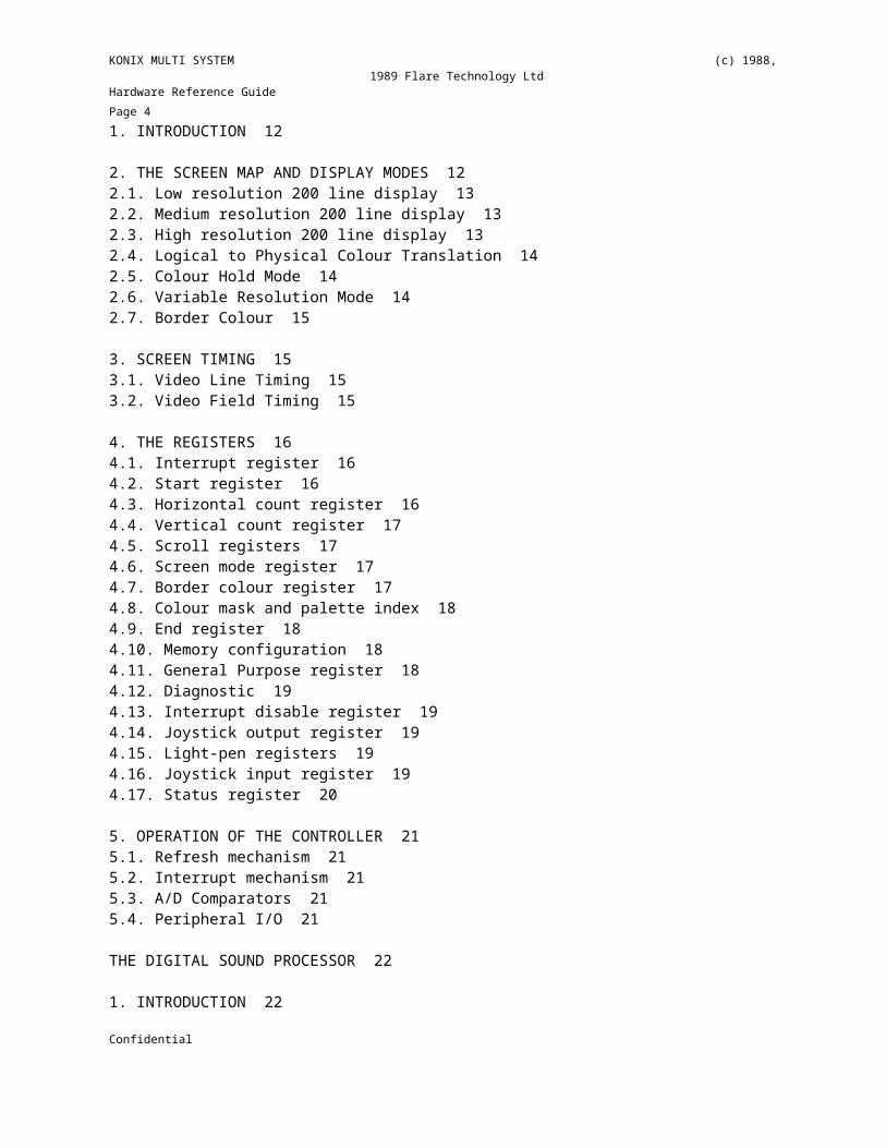
TABLE OF CONTENTS Confidential

KONIX MULTI SYSTEM (c) 1988, 1989 Flare Technology LtdHardware Reference Guide Page 3
DISCLAIMER AND WARNINGS 2
TABLE OF CONTENTS 3
THE KONIX MULTI SYSTEM 6
1. INTRODUCTION 61.1. This Document 6
2. ARCHITECTURE 62.1. Memory Map 82.2. I/O Map 92.3. Memory Interface Timing 102.4. Video Cycles 102.5. 8086 CPU cycles 10
THE VIDEO CONTROLLER 12
1. INTRODUCTION 12
2. THE SCREEN MAP AND DISPLAY MODES 122.1. Low resolution 200 line display 132.2. Medium resolution 200 line display 132.3. High resolution 200 line display 132.4. Logical to Physical Colour Translation 142.5. Colour Hold Mode 142.6. Variable Resolution Mode 142.7. Border Colour 15
3. SCREEN TIMING 153.1. Video Line Timing 153.2. Video Field Timing 15
4. THE REGISTERS 164.1. Interrupt register 164.2. Start register 164.3. Horizontal count register 164.4. Vertical count register 174.5. Scroll registers 174.6. Screen mode register 174.7. Border colour register 174.8. Colour mask and palette index 184.9. End register 184.10. Memory configuration 184.11. General Purpose register 184.12. Diagnostic 194.13. Interrupt disable register 194.14. Joystick output register 194.15. Light-pen registers 194.16. Joystick input register 194.17. Status register 20
5. OPERATION OF THE CONTROLLER 21Confidential
KONIX MULTI SYSTEM (c) 1988, 1989 Flare Technology LtdHardware Reference Guide Page 4
5.1. Refresh mechanism 215.2. Interrupt mechanism 215.3. A/D Comparators 215.4. Peripheral I/O 21
THE DIGITAL SOUND PROCESSOR 22
1. INTRODUCTION 22
2. ARCHITECTURE 222.1. ALU 232.2. Multiplier 242.3. DMA Channel 24
3. MEMORY 25
4. DSP INSTRUCTION SET 274.1. Conditional Instructions 274.2. Indexed Addressing 274.3. Opcodes 27
5. HOST MEMORY MAP 29
6. DATA TRANSFER BETWEEN HOST AND DSP 306.1. Under DSP control - DMA transfer 306.2. Under Host Control - INTRUDE 32
7. ILLEGAL INSTRUCTION COMBINATIONS 337.1. Multiply / Multiply-Accumulate operations 337.2. DAC instructions 33
THE BLITTER 34
1. INTRODUCTION 341.1. This Section 341.2. The Blitter 34
2. ARCHITECTURE 342.1. Overview 342.2. The Data Path 352.3. The Address Generator 382.4. The Sequencer 392.5. Memory Interface and Interrupts 45
3. MODES OF OPERATION 463.1. Simple Memory Fill and Copy Operations 463.2. Line Drawing 473.3. Example Program 493.4. Character Painting 50
4. BLITTER COMMAND FORMAT 524.1. Command and Mode Control Bits 534.2. Step Register and Enhanced Step Control Bits 544.3. Comparator Control Bits 54Confidential

KONIX MULTI SYSTEM (c) 1988, 1989 Flare Technology LtdHardware Reference Guide Page 5
4.4. Logic Function Unit Control Bits 544.5. Source Address Register and Control Bits 554.6. Destination Address Register and Control Bits 554.7. Program Address Register 55
5. BLITTER I/O REGISTERS 565.1. Destination Register 0 565.2. Destination Register 1 565.3. Source Register 0 565.4. Source Register 1 575.5. Blitter Program Address 575.6. Blitter Command Register 575.7. Blitter Control Register 58
THE DISK CONTROLLER 59
1. INTRODUCTION 591.1. Disk Format 591.2. Read Operation 591.3. DMA Interface 601.4. Block Diagram 601.5. Write Operation 60
2. REGISTERS 612.1. Floppy Disk Control Register 612.2. Disk Status Port 622.3. Drive Control Register 632.4. Drive Status Port 63
3. ERROR HANDLING AND DATA INTEGRITY 64
APPENDICES 65
A. The DSP Arithmetic Logic Unit 65
B. The DSP Assembler Manual 661. How to invoke the assembler 662. Source File format 663. Error Reporting 71
THE KONIX MULTI SYSTEMConfidential

KONIX MULTI SYSTEM (c) 1988, 1989 Flare Technology LtdHardware Reference Guide Page 6
1. INTRODUCTION
The Konix Multi System is designed to be an ultra-high performance arcade games engine. It achieves this by utilising three processors, one general purpose processor, an Intel 8086, and two highly specialised co-processors, the Blitter and the DSP.The system is intended to be as simple as possible, while still providing the necessary performance levels (compare the complexity of the Amiga); and to provide as much flexibility as the programmer may wish.
1.1 This Document
This document is intended to be a useful guide to the assembly language programmer who wishes to drive the hardware facilities provided in an effective manner. It is not for novices.This first section discusses the computer system as a whole, and is followed by individual sections discussing each sub-module. The best approach is to read it through first, then to approach it as a reference guide once the overall context of sections is understood.
Confidential

KONIX MULTI SYSTEM (c) 1988, 1989 Flare Technology LtdHardware Reference Guide Page 7
2. ARCHITECTURE
The Konix Multi System computer electronics are largely contained within one massive custom logic chip, known as an ASIC (for Application Specific Integrated Circuit). The system memory and 8086 CPU lie outside the ASIC. This diagram summarises the architecture:
Video ┌─────────────║─────┐┌────────────┐ │ ┌───────────╨─┐ │ ┌──────────┐│8086 CPU ╞══════╡Video/Memory ╞═══════════╡Screen ││6 MHz │ │ │Controller │ ║ │ ║ │RAM │└────────────┘ │ └─────────────┘ ║ │ ║ └──────────┘ │ ┌─────────────┐ ║ │ ║ │ │Floppy Disk ╞═╣ │ ║ ┌──────────┐ │ │Read DMA │ ║ │ ╠════╡System │ │ └─────────────┘ ║ │ ║ │RAM │ │ ┌─────────────┐ ║ │ ║ └──────────┘ │ │Blitter ╞═╣ │ ║ │ │Co-processor │ ║ │ ║ ┌──────────┐ │ └─────────────┘ ║ │ ╚════╡Bootstrap │ │ ┌─────────────┐ ║ │ │ROM │ │ │DSP ╞═╝ │ └──────────┘ │ │Processor ╞═══════╗ │ └──╥────────╥─┘ │ Audio │ ┌──╨────────╨─┐ │ │ │DSP 32-bit │ │ │ │ROM and RAM │ │ │ └─────────────┘ │ │ASIC │ └───────────────────┘
Sharing the main memory bus are four bus masters; the DSP, the Floppy Disk Interface, the Blitter and the 8086. Only one of the bus masters may own the bus at any one time, and a priority for the bus exists, giving the DSP highest priority, followed by the Floppy Disk Controller, the Blitter and the CPU, in descending order.
The video controller controls the bus, and provides the memory timing signals for memory devices attached to the bus. It also requires memory cycles, and has effectively the highest priority on the bus. It will suspend bus master operations during video lines for brief periods to fetch video display data, and to refresh dynamic RAM. It interfaces with the 8086 CPU, and performs the bus de-multiplexing for it.
The DSP is a simple, very high-speed processor for sound synthesis; operating at 12 MIPs. It has access to the main bus via a DMA controller which allows it to read and write bytes or words from main memory. These transfers occur in short bursts, and are under DSP program control. The DSP actually executes programs and stores data in its own private high speed memory.
Confidential

KONIX MULTI SYSTEM (c) 1988, 1989 Flare Technology LtdHardware Reference Guide Page 8
The Floppy Disk Read DMA channel allows the system to transfer floppy disk read data into main memory without any software overhead.The Blitter is a graphics processor for fast screen updates and animation, acting as a hardware graphics sub-routine for the 8086. It will become bus master throughout a Blitter program operation, and may therefore own the bus for considerable periods. However, its priority over the CPU is not total, as it may be requested to give up the bus to the CPU when an interrupt occurs.The 8086 CPU is the lowest priority bus master at the system level, but has complete control of the other two processors, and so the use of the bus is entirely under program control.
2.1 Memory Map
Two memory maps are supported by the system. Selection of them is described below in the Video Controller section.
Map 0 Map 1 FFFFF ┌──────────────────┐ ┌──────────────────┐ │ │ │ │ │ 16-bit │ │ 16-bit │ │ ROM │ │ ROM │ │ │ │ │ C2000 ├──────────────────┤ ├──────────────────┤ │reserved │ │reserved │ C1600 ├──────────────────┤ ├──────────────────┤ │DSP Program RAM │ │DSP Program RAM │ C1400 ├──────────────────┤ ├──────────────────┤ │DSP Data RAM │ │DSP Data RAM │ C1300 ├──────────────────┤ ├──────────────────┤ │DSP Registers │ │DSP Registers │ C1280 ├──────────────────┤ ├──────────────────┤ │DSP Data Constants│ │DSP Data Constants│ C1200 ├──────────────────┤ ├──────────────────┤ │DSP Data ROM │ │DSP Data ROM │ C1000 ├──────────────────┤ ├──────────────────┤ │reserved │ │reserved │ C0200 ├──────────────────┤ ├──────────────────┤ │Palette RAM │ │Palette RAM │ C0000 ├──────────────────┤ ├──────────────────┤ │ │ │ │ │ 16-bit │ │ 16-bit │ │ Screen RAM │ │ System RAM │ │ │ │ │ 80000 ├──────────────────┤ │ │ │ │ │ │ │ 16-bit │ │ │ │ System RAM │ │ │ │ │ │ │ 40000 │ │ ├──────────────────┤ │ │ │ │ │ │ │ 16-bit │ │ │ │ Screen RAM │ │ │ │ │Confidential

KONIX MULTI SYSTEM (c) 1988, 1989 Flare Technology LtdHardware Reference Guide Page 9
00000 └──────────────────┘ └──────────────────┘
Map one is the most useful arrangement for the standard machine as it provides RAM at 00000 for the vectors. In it the one Megabyte memory space is divided into four logical areas, with the 256K area based at 00000h allocated for internal 16-bit screen RAM, the 512K area based at 40000h for expansion RAM, the 8K byte area of memory based at C0000h is the internal memory of the ASIC, and the 248K area based C2000h is ROM.
2.2 I/O Map
Address Write Register Read Register 00 Interrupt line Horizontal light-pen02 - Vertical light-pen04 Screen start -08 Horizontal counter Joystick inputs0C Vertical counter Machine status10 Scroll register 1 -12 Scroll register 2 -14 Scroll register 3 -16 Interrupt acknowledge -18 Screen mode -1A Border colour -1E Colour mask -20 Palette index -22 Screen end -26 Memory configuration -28 General purpose -2A Diagnostic -2C Interrupt disable -2E Joystick outputs -40 Blitter program address Blitter destination address 042 Blitter command Blitter destination address 144 Blitter control Blitter source address 046 - Blitter source address 148 Floppy read control Floppy read status80 Drive control Drive status88-8F General purpose I/O decode 190-97 General purpose I/O decode 298-9F General purpose I/O decode 3A0-FF Free for third party peripheral I/O
The 8086 I/O space is internally decoded to eight bits, as shown above. I/O locations above A0h are free for third party I/O expansion. In addition to this, three spare general purpose I/O decodes are provided - these may be used to provide an active low chip enables to external devices, note that RD and WR should also be connected to the devices.All internal I/O locations are on even boundaries, and word wide I/O reads and write may be performed where appropriate. Do not perform byte wide I/O writes on word-wide write registers, and do not perform any I/O cycles to odd addresses.All locations marked with a dash “-” are reserved for future expansion or Confidential

KONIX MULTI SYSTEM (c) 1988, 1989 Flare Technology LtdHardware Reference Guide Page 10 manufacturing test modes. Do not write to any of these locations or use them for external I/O.
Analogue Inputs
In addition to switch controls, the machine has three potentiometer based analogue controls, and a light-pen type input.The potentiometer output voltages are measured by comparing them to a voltage ramp which is reset every vertical video synchronization pulse. When the potentiometer voltage equals the ramp voltage an interrupt is generated, one interrupt being generated in every video frame for each of the analogue inputs. When one of these interrupts occurs, the CPU may read the video vertical counter, #and from this estimate the analogue voltage being measured. The interrupt mechanism is described in greater detail in the Video Controller section below.When a second machine is connected in slave mode, its potentiometer values may also be read, as an analogue multiplexer selects between the internal potentiometers, and a second set connected to the joystick port. In this mode, the two sets of potentiometers would be read on alternate video fields. It is also possible that other analogue controls might be attached to the joystick port, and these would be read in a similar manner. The analogue multiplexer control line is in the General Purpose register.A light-pen, or other beam detecting device such as a gun, may also be connected. This function is part of the Video Controller described below.
Memory Interface Timing
All memory timing is based on a single master clock rate, which is either four times the European PAL TV standard chroma carrier frequency, or five times the American NTSC TV standard chroma carrier frequency. These give master clock rates of:
NTSC 17.897725 MHzPAL 17.734475 MHz
This clock rate is divided by 1.5 to produce the co-processor and memory interface clock, nominally 12 MHz. This is further divided by 2 to give the processor clock, nominally 6 MHz.In the descriptions below timings either apply to both systems, or two numbers are given, the second one in brackets being the NTSC system figure.
Video Cycles
The memory interface is available to the current bus master throughout it’s ownership, except during video cycles. When video data is being fetched or dynamic RAM is being refreshed, wait states may be inserted into co-processor memory cycles. This mechanism does not affect the CPU. Video lines are nominally 64(63.5) micro-seconds, and 44 of these are used for video or refresh. This mechanism is described in greater detail in the Video Controller section.Confidential

KONIX MULTI SYSTEM (c) 1988, 1989 Flare Technology LtdHardware Reference Guide Page 11
8086 CPU cycles
All CPU memory cycles take place in four processor clock ticks, with no wait states inserted, in all the types of memory available (this gives a memory cycle time of 670 ns or about 1.5 MHz). However, Refresh the video controller requires that all CPU cycles occur on a 4 T-state boundary, and may insert wait states to align the processor cycle onto a four T-state boundary, i.e. up to three wait cycles may occur.This alignment operation, once it has occurred, will not cause any further wait states as long as the processor continues to request memory cycles every four T-states. Should its bus interface pause, then it will have to pause for a multiple of 4 T-states.It is expected that the action of the pre-fetch queue of the processor will largely hide these wait states, and prevent them from affecting program execution speed, so that delays on software execution time due to this mechanism will be small.
Co-Processor Cycles
The Blitter, the DSP, and the Floppy Disk Controller will all perform memory cycles in two 12 MHz clock cycles when possible. Co-processor memory cycles into Static RAM and Pseudo-Static RAM (fast RAM) will take two 12 MHz cycles, co-processor #memory cycles into ROM and Dynamic RAM will take three 12 MHz cycles (slow RAM or ROM).The screen RAM will always be 16-bit fast RAM. The system RAM area may contain slow or fast memory. The ASIC internal RAM area based at C0000h looks like 16-bit fast RAM (but see notes below about its availability). The area at C2000h will contain 16-bit slow ROM.Unlike the CPU, co-processors are affected by video lines. During video fetch, four 12 MHz clock cycles out of every eight are occupied by video data fetch operations. The remaining four clock cycles offer a `slot' into which two fast memory cycles or one slow memory cycle may drop. In lo-res, four clock cycles out of every sixteen are occupied, leaving a twelve clock cycle slot. The co-processor will have WAIT states injected into its memory cycles until a slot is available.Therefore 4/8 or 50% of the bus bandwidth is available to the co-processors in fast RAM during video or refresh lines, and 3/8 or 37.5% is available in slow RAM (more are available in lo-res). These restrictions only occur during video fetch, which is 44us out of a 64us video line. Taking as an example a PAL screen of 200 lines (in a312 line field), this gives:
4 x 44 x 200 = 22% lost in fast RAM8 64 312
This gives the Blitter a bus rate of 4.6 million memory cycles per second, i.e. a rate of 9.2 Megabytes per second into 16-bit RAM, giving it the ability to block fill a 50K screen in 5.4 milliseconds.
Confidential

KONIX MULTI SYSTEM (c) 1988, 1989 Flare Technology LtdHardware Reference Guide Page 12
Bus Latency
When a co-processor requests the bus from the CPU, there is a finite period before the bus is granted by the processor HLDA signal, and this period is the bus latency. This latency is particularly relevant to DSP programmers. The Intel 8086 has a maximum latency of twelve processor clock cycles, which is twenty-four co-processor clock cycles.The actual latency figure is worse, due to the potential for wait-states on the bus latency period, and because of the internal bus arbitration logic. This may add up to another six co-processor clock cycles in the worst case. This means the worst case bus latency, from asserting HOLD to being granted the bus, is thirty co-processor clock cycles.DSP programmers will therefore have to place thirty DSP instructions between requesting the bus by a write to the DMA1 register, and initiating a memory transfer by a write to the DMA0 register.
THE VIDEO CONTROLLER
INTRODUCTION
This section describes the Konix Multi System video block. The video block has the following functions :-
1) To provide DRAM timing on behalf of the processors2) To generate video and refresh cycles3) To generate video timing and support gen-locking4) To convert video memory contents to pixel data.5) To generate an interrupt at a given display line.6) To latch the presence and position of a light-pen signal7) To control data and address bus buffers8) To vector interrupts9) To provide I/O to Konix Multi System peripherals
THE SCREEN MAP AND DISPLAY MODES
The screen may begin on any 256 byte boundary in 16 bit memory, (0-256k). The number of screen lines is programable between 1 and 256 lines. The address of the top left pixel is given by the vertical and horizontal scroll registers. The horizontal scroll register gives the least significant eight bits. The vertical scroll register gives the most significant ten bits.
Two national television standards are supported:
Lines Field rate Crystal frequencyPAL 312 50 Hz 17.734475 MHzNTSC 262 60 Hz 17.897725 MHz
Both produce non-interlaced displays. The selection of a default standard is determined by the state of a pin during reset, and this state may be read by software to determine which variant it is running on. The standard may also be changed by software. The crystal frequency is
Confidential

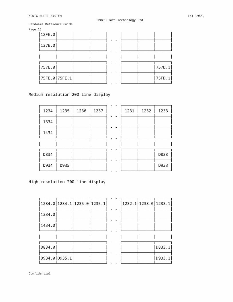
KONIX MULTI SYSTEM (c) 1988, 1989 Flare Technology LtdHardware Reference Guide Page 13 divided by 1.5 to give a video timing frequency referred to as 12 MHz for convenience.Three resolutions are supported low, medium and high.In low resolution the screen is 256 pixels wide, the pixel rate is 6Mhz and pixels are represented by nibbles. In medium resolution the screen is 256 pixels wide, the pixel rate is 6 MHz and pixels are represented by bytes. In high resolution the screen is 512 pixels wide, the pixel rate is 12 Mhz and pixels are represented by nibbles.The mapping between pixels and memory addresses is as follows. For convenience the horizontal scroll register contains 7E and the vertical scroll register contains 12. The top left pixel comes from address 0127E.127E.0 refers to the less significant nibble at address 127E.127E.1 refers to the more significant nibble.
Low resolution 200 line display
┌──────┬──────┬──────┬──────┐ - - ┌──────┬──────┬──────┐ │127E.0│127E.1│127F.0│127F.1│ │127C.1│127D.0│127D.1│ ├──────┼──────┼──────┼──────┤ - - ├──────┼──────┼──────┤ │12FE.0│ │ │ │ │ │ │ │ ├──────┼──────┼──────┼──────┤ - - ├──────┼──────┼──────┤ │137E.0│ │ │ │ │ │ │ │ └──────┴──────┴──────┴──────┘ - - └──────┴──────┴──────┘ | | | | | | | | | ┌──────┬──────┬──────┬──────┐ - - ┌──────┬──────┬──────┐ │757E.0│ │ │ │ │ │ │757D.1│ ├──────┼──────┼──────┼──────┤ - - ├──────┼──────┼──────┤ │75FE.0│75FE.1│ │ │ │ │ │75FD.1│ └──────┴──────┴──────┴──────┘ - - └──────┴──────┴──────┘
Medium resolution 200 line display
┌──────┬──────┬──────┬──────┐ - - ┌──────┬──────┬──────┐ │ 1234 │ 1235 │ 1236 │ 1237 │ │ 1231 │ 1232 │ 1233 │ ├──────┼──────┼──────┼──────┤ - - ├──────┼──────┼──────┤ │ 1334 │ │ │ │ │ │ │ │ ├──────┼──────┼──────┼──────┤ - - ├──────┼──────┼──────┤ │ 1434 │ │ │ │ │ │ │ │ └──────┴──────┴──────┴──────┘ - - └──────┴──────┴──────┘ | | | | | | | | | ┌──────┬──────┬──────┬──────┐ - - ┌──────┬──────┬──────┐ │ D834 │ │ │ │ │ │ │ D833 │ ├──────┼──────┼──────┼──────┤ - - ├──────┼──────┼──────┤ │ D934 │ D935 │ │ │ │ │ │ D933 │ └──────┴──────┴──────┴──────┘ - - └──────┴──────┴──────┘
High resolution 200 line display
┌──────┬──────┬──────┬──────┐ - - ┌──────┬──────┬──────┐ │1234.0│1234.1│1235.0│1235.1│ │1232.1│1233.0│1233.1│ ├──────┼──────┼──────┼──────┤ - - ├──────┼──────┼──────┤ │1334.0│ │ │ │ │ │ │ │Confidential

KONIX MULTI SYSTEM (c) 1988, 1989 Flare Technology LtdHardware Reference Guide Page 14 ├──────┼──────┼──────┼──────┤ - - ├──────┼──────┼──────┤ │1434.0│ │ │ │ │ │ │ │ └──────┴──────┴──────┴──────┘ - - └──────┴──────┴──────┘ | | | | | | | | | ┌──────┬──────┬──────┬──────┐ - - ┌──────┬──────┬──────┐ │D834.0│ │ │ │ │ │ │D833.1│ ├──────┼──────┼──────┼──────┤ - - ├──────┼──────┼──────┤ │D934.0│D935.1│ │ │ │ │ │D933.1│ └──────┴──────┴──────┴──────┘ - - └──────┴──────┴──────┘
The number of screen lines is determined by the START and END registers.Note that screen lines wrap within a page given by the line-size. Lo-res lines wrap within 128-byte pages, and medium and hi-res lines wrap within 256-byte pages.
Logical to Physical Colour Translation
The physical colour is made from four bits of each of red, green and blue. The logical colour is determined by either a byte or a nibble in memory. The mapping between logical and physical colour is performed by a colour look up table or palette.Any bits in the logical colour may be sacrificed, and replaced by bits from the palette index register. For every bit set in the pixel mask register the corresponding bit in the logical colour is replaced by a bit from the palette index register. The unused (or masked) bits may be used elsewhere, e.g. by the Blitter for depth information.Where the logical colour is derived from a nibble in memory the top four bits are deemed to be zeroes. The mask register would normally mask out these bits in this case, allowing the palette index register to select one of 16 palettes.The most significant bit of each pixel may also be used by the video block. It can be made available on the encrustation output to embed the locally generated picture onto an external video source (Bit set selects the local picture). The encrustation output may also be used to strobe frame grabbing AD convertors. It can also be used in variable-mode to determine whether the current byte is displayed as one med-res pixel or two hi-res pixels. See the section below.The palette memory appears in the memory map of the host processor from C0000 to C01FF. Each word has the following meaning.
┌──┬──┬──┬──┬──┬──┬──┬──┬──┬──┬──┬──┬──┬──┬──┬──┐MSB │--│--│--│--│r3│r2│r1│r0│g3│g2│g1│g0│b3│b2│b1│b0│ LSB └──┴──┴──┴──┴──┴──┴──┴──┴──┴──┴──┴──┴──┴──┴──┴──┘
Where r3 is the most significant red bit of the physical colour. The word at address C0000 corresponds to logical colour 0, The word at address C0002 corresponds to logical colour 1 etc.
The palette should only be read or written while the display is inactive, i.e. during line or frame border and flyback periods.
Colour Hold ModeConfidential

KONIX MULTI SYSTEM (c) 1988, 1989 Flare Technology LtdHardware Reference Guide Page 15
In colour hold mode logical colour zero is elected to be `transparent'. This colour is replaced by the previously displayed non-transparent colour. This display scheme may be used to fill large areas with colour by simply drawing their outline.
Note that the left side should be drawn in the fill colour, and the right side should be drawn in the required background colour. If the first pixel displayed on a line is transparent, then the colour held is undefined.
Variable Resolution Mode
Variable resolution mode allows the screen mode to be changed from high resolution to medium resolution on a byte by byte basis. In variable resolution mode the top bit of each byte of screen data determines whether the data will be two high resolution pixels (1) or one medium resolution pixel (0).The loss of this bit means that the medium resolution pixel will have logical colours 0-127 available, and the high resolution pixels will have logical colours 0-15 available to the left one and 8-15 available to the right one derived from each byte.
Border Colour
A border register determines the physical colour of picture outside the computer screen.
SCREEN TIMING
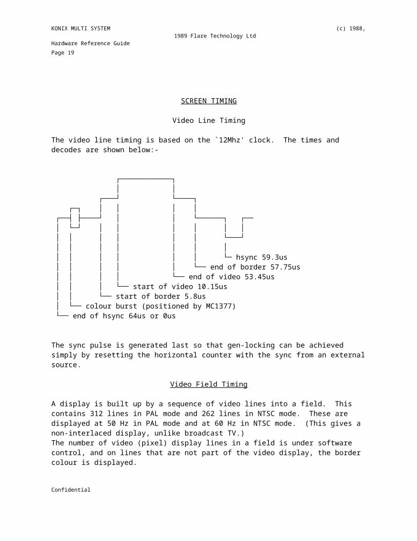
Video Line Timing
The video line timing is based on the `12Mhz' clock. The times and decodes are shown below:-
┌────────────┐Confidential
KONIX MULTI SYSTEM (c) 1988, 1989 Flare Technology LtdHardware Reference Guide Page 16 │ │ ┌───┘ └────┐ ┌─┐ │ │ │ │ ┌──┤ ├────┘ │ │ └──────┐ ┌── │ └─┘ │ │ │ │ │ │ │ │ │ │ │ │ └───┘ │ │ │ │ │ │ │ │ │ │ │ │ │ └─ hsync 59.3us │ │ │ │ │ └── end of border 57.75us │ │ │ │ └── end of video 53.45us │ │ │ └── start of video 10.15us │ │ └── start of border 5.8us │ └── colour burst (positioned by MC1377) └── end of hsync 64us or 0us
The sync pulse is generated last so that gen-locking can be achieved simply by resetting the horizontal counter with the sync from an external source.
Video Field Timing
A display is built up by a sequence of video lines into a field. This contains 312 lines in PAL mode and 262 lines in NTSC mode. These are displayed at 50 Hz in PAL mode and at 60 Hz in NTSC mode. (This gives a non-interlaced display, unlike broadcast TV.)The number of video (pixel) display lines in a field is under software control, and on lines that are not part of the video display, the border colour is displayed.Not all the actual display lines in the field are visible. Some are occupied by `flyback', a period in which the beam is moved back from the bottom of the screen to the top, and some are lost at the top and bottom due to `overscan', which occurs as the picture fills the whole screen and overflows it slightly (on broadcast TV some of these are used for teletext).In PAL mode, more than 256 lines may be visible on some displays. However, software that takes advantage of this will not be compatible with the NTSC standard as some of these lines are lost to overscan on an NTSC set. Therefore the maximum number of lines used should be rather less.A sensible maximum is about 200 lines visible; for example the MSX standard allows 212, and this should probably be treated as a maximum.
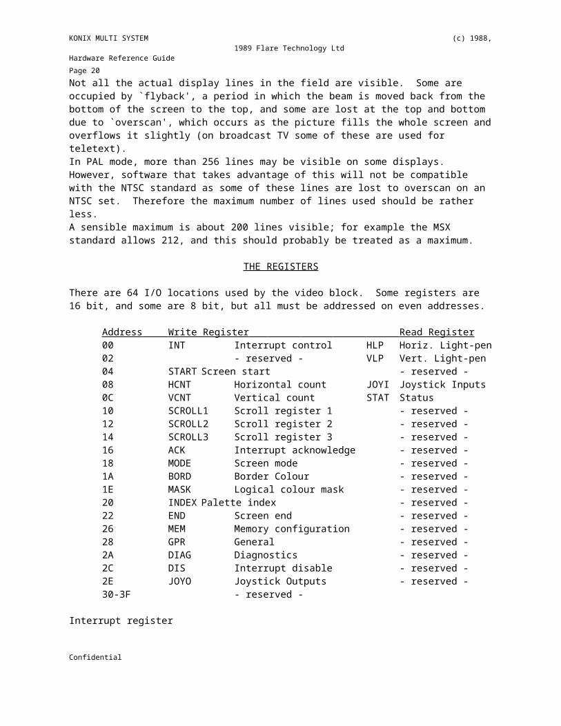
THE REGISTERS
There are 64 I/O locations used by the video block. Some registers are 16 bit, and some are 8 bit, but all must be addressed on even addresses.
Address Write Register Read Register 00 INT Interrupt control HLP Horiz. Light-pen02 - reserved - VLP Vert. Light-pen04 START Screen start - reserved -08 HCNT Horizontal count JOYI Joystick Inputs0C VCNT Vertical count STAT Status
Confidential

KONIX MULTI SYSTEM (c) 1988, 1989 Flare Technology LtdHardware Reference Guide Page 17
10 SCROLL1 Scroll register 1 - reserved -12 SCROLL2 Scroll register 2 - reserved -14 SCROLL3 Scroll register 3 - reserved -16 ACK Interrupt acknowledge - reserved -18 MODE Screen mode - reserved -1A BORD Border Colour - reserved -1E MASK Logical colour mask - reserved -20 INDEX Palette index - reserved -22 END Screen end - reserved -26 MEM Memory configuration - reserved -28 GPR General - reserved -2A DIAG Diagnostics - reserved -2C DIS Interrupt disable - reserved -2E JOYO Joystick Outputs - reserved -30-3F - reserved -
Interrupt register
INT 00hACK 16h
INT determines the screen line at which an interrupt is generated. The interrupt is generated just after the active video area on that line. Zeroes should be written into the top seven bits of INT. This interrupt is associated with interrupt vector 21h. The interrupt is cleared by writing anything to the ACK port.
Start register
START 04h
This register determines the screen line at which the video display begins. Zeroes should be written into the top seven bits of START. The display begins on the line after the specified line.
Horizontal count register
HCNT 08h
When a word is written into HCNT the horizontal time-base counter is loaded with this value. This is mainly useful for test purposes.In PAL mode the counter counts up from 0 (just after hsync) to 756 (the end of hsync). The active display area is from 120 to 631 inclusive. The counter counts in units of one hi-res pixel (11.82MHz).
Vertical count register
VCNT 0Ch
When a byte is written into this VCNT the vertical time-base counter is loaded with this value. Again this is mainly useful for test purposes.In PAL mode the counter counts up from 0 (just after vsync) to 311 (the end of vsync). The active display area is from 33 to 288 inclusive. The counter counts in display lines (15.625Khz).Confidential

KONIX MULTI SYSTEM (c) 1988, 1989 Flare Technology LtdHardware Reference Guide Page 18
Scroll registers
SCROLL1 10hSCROLL2 12hSCROLL3 14h
These three registers determine the address, within the first 256k of memory, of the top left pixel. SCROLL1 gives the bottom eight bits, SCROLL2 gives the next eight bits and bits 0 & 1 of SCROLL3 give the top two bits. Zeroes should be written to the top six bits of SCROLL3.All three registers should be written, in ascending order.The screen must begin on a word boundary, so the bottom bit of SCROLL1 is ignored. Note also that the data for one line will lie within a 128 or 256 byte field depending on the screen mode, and therefore the line will wrap in this area if the start is not on the boundary.
Screen mode registerMODE 18h
This register contains various bits controlling the screen mode:
Bits 0,1 Determines the screen mode, 0 is low resolution, 1 is medium resolution, 2 is high resolution, 3 is unused.
Bit 2 Enables gen-locking. When enabled hsync and vsync become inputs and the video time-base generators are reset by these inputs.
Bit 3 Enables encrustation. If zero the local display is enabled. If one the local pixels are enabled if the most significant bit of each pixel is set.
Bit 4 Enables encrustation of the border. If encrustation is enabled this bit enables the local border colour.
Bit 5 Enables colour hold mode.
Bit 6 Enables variable resolution mode.
Bit 7 Enables the screen to cross 64k boundaries. This may be used if more than 64k of screen ram is installed.
Border colour register
BORD 1Ah
These registers give the physical border colour. The registers define red, green and blue intensities like the palette RAM. ie:-
BORD ┌──┬──┬──┬──┬──┬──┬──┬──┬──┬──┬──┬──┬──┬──┬──┬──┐MSB │--│--│--│--│r3│r2│r1│r0│g3│g2│g1│g0│b3│b2│b1│b0│ LSB └──┴──┴──┴──┴──┴──┴──┴──┴──┴──┴──┴──┴──┴──┴──┴──┘Confidential
KONIX MULTI SYSTEM (c) 1988, 1989 Flare Technology LtdHardware Reference Guide Page 19
Zeroes should be written to the top four bits of BORD.
Colour mask and palette index
MASK 1EhINDEX 20h
These registers allow bits in a pixel’s logical colour to be sacrificed for other purposes. For each bit set in the mask register the corresponding bit in the logical colour is replaced by a bit from the palette index register. For instance say the most significant bit is used by the Blitter for depth information. The mask register would be set to 80h giving two palettes of 128 colours selected by the most significant bit of the palette index register.
End register
END 22h
This register specifies the last active display line.
Memory configuration
MEM 26h
This register determines the position of screen memory and the position and type of the 512k expansion memory.
Bits 0,1 These determine the type of expansion memory as follows:- 0 is ROM(default), 1 is DRAM, 2 is SRAM, 3 is PSRAM.
Bit 2 This determines the position of screen ram and expansion ram as follows.
Bit 2 reset (default) Bit 2 set
MAP ZERO MAP ONE
┌─────┐ ┌─────┐ │ ROM │ C2000h-FFFFFh │ ROM │ C2000h-FFFFFhConfidential
KONIX MULTI SYSTEM (c) 1988, 1989 Flare Technology LtdHardware Reference Guide Page 20 ├─────┤ ├─────┤ │ DSP │ C1000h-C1FFFh │ DSP │ C1000h-C1FFFh ├─────┤ ├─────┤ │ PAL │ C0000h-C0FFFh │ PAL │ C0000h-C0FFFh ├─────┤ ├─────┤ │ SCR │ 80000h-BFFFFh │ │ ├─────┤ │ EXP │ │ │ │ MEM │ 40000h-BFFFFh │ EXP │ │ │ │ MEM │ 00000h-7FFFFh ├─────┤ │ │ │ SCR │ 00000h-3FFFFh └─────┘ └─────┘
Bits 3-7 These should be programmed with zeroes.
General Purpose register
GPR 28h
This register provides general purpose output.
Bit 0 Analogue input select. When set this selects the second set of analogue inputs.
Bit 1 This enables the DSP output.
Bit 2 Joystick output 8
Bits 3-7 Set to zero.
Diagnostic
DIAG 2Ah
This register contains some general control bits, as well as some diagnostic functions relevant only to chip testing.
Bit 0 When set this bit lets the light-pen registers reflect the current position of the electron beam. This bit is cleared by reset.
Bit 1 When set NTSC mode is used. This is set or cleared during reset and may be read in the status port.
Bit 2 Set to zero.Bit 3 Set to zero.Bit 4 When set the screen mode is updated immediately when written
and the palette is made transparent.Bits 5-7 Set to zero.
Interrupt disable register
DIS 2Ch
This register selectively disables the interrupt sources.
Confidential

KONIX MULTI SYSTEM (c) 1988, 1989 Flare Technology LtdHardware Reference Guide Page 21 Bit 0 Disables the video interrupt.Bits 1-3 Disable analogue inputs 0 to 2.Bit 4 Disables floppy disk interrupt.Bits 5-7 Set to zero.
Joystick output register
JOYO 2Eh
This register provides general purpose outputs.
Bits 0-7 Joystick outputs 0-7
Light-pen registers
HLP 00hVLP 02h
These registers determine the current position of the light-pen or electron beam depending on the state of bit 0 in DIAG.HLP gives the horizontal count. VLP gives the vertical count. Light-pens produce well defined rising edges but slow decays and respond to several display lines. The value latched is the value at the leading edge of the first pulse each frame. A latch is cleared at the start of each frame (at the end of vsync) and is set by the arrival of the light-pen pulse. The state of this latch can be read in the status register.
Joystick input register
JOYI 08h
This register provides general purpose inputs.
Bits 0-15 Joystick inputs 0-15
Status register
STAT 0Ch
This register allows various status bits of the controller to be read.
Bit 0 This bit is set if the machine is configured for NTSC.Bit 1 This bit is set if a light pen pulse has been received.Bit 2 This bit is set if the processor is working at 9MHz.Bits 3-5 Joystick Inputs 16-18Bit 6 Floppy disk index pulseBit 7 Reserved
OPERATION OF THE CONTROLLER
Refresh mechanismConfidential

KONIX MULTI SYSTEM (c) 1988, 1989 Flare Technology LtdHardware Reference Guide Page 22
Dynamic and Pseudo static memory are refreshed by the video fetch mechanism. DRAM is refreshed by one CAS before RAS cycle for each four bytes fetched. PSRAM is refreshed by two OE cycles. Because the screen size may be adjusted by the program the video fetch mechanism is always active on certain lines. In low res. it is active for four lines every 64 lines; i.e. 0-3,64-67,128-131 etc. In medium and high res. it is active for two lines every 64 lines.
Interrupt mechanism
There are five interrupt sources within the Konix Multi System ASIC. One video interrupt, three interrupts from the comparator inputs and the floppy interrupt. Each has its own vector. The video interrupt uses vector 21h, the comparators use vectors 22h to 24h and the floppy uses vector 25h. If an external interrupt occurs vector 20h is supplied. Interrupts with lower vectors have higher priority. Interrupts are cleared by writing to the ACK port. If several interrupts occur together each will generate an interrupt and each must be acknowledged.
A/D Comparators
In order to measure analogue voltages economically three comparator inputs are provided. The external comparators should compare the voltage to be measured against a ramp triggered by vertical sync. Negative transitions cause a vectored interrupt allowing the 8086 to read the line number and estimate the voltage.
Peripheral I/O
Four I/O locations are decoded for general purpose use:-
GPIO 0 I/O 80h-87h (drive control)GPIO 1 I/O 87h-8FhGPIO 2 I/O 90h-97hGPIO 3 I/O 98h-9Fh
All undefined I/O locations between 0 and 7Fh are reserved for future expansion. I/O locations above 9Fh are available for third party peripherals. Note that GPIO 0 is used for the floppy drive control functions and is unavailable for external use.
Confidential

KONIX MULTI SYSTEM (c) 1988, 1989 Flare Technology LtdHardware Reference Guide Page 23
THE DIGITAL SOUND PROCESSOR
INTRODUCTION
The DSP system in the Konix Multi System is a general purpose arithmetic processor with sufficient power to implement a high performance music synthesizer. Pulse width modulated outputs are provided for generation of stereo audio signals with 14 bit precision and hence approaching the sort of sound quality normally associated with Compact Disk technology.The DSP is micro-programmable from the host CPU and the instruction set is sufficiently flexible to enable the user to program the device to fulfill many different functions that are considerably at variance with that of `music synthesizer'. Such applications might include algorithmic speech generation and audio analysis using fast fourier transform techniques.The DSP uses Harvard Architecture for maximum data throughput (separate program and data buses).The ALU features a hardware 16 x 16 hardware multiply/accumulate as well as addition, subtraction and logical functions. The carry bit from the adder/subtractor is stored in a separate latch and can be either used either to propagate carry for multiple precision arithmetic or can be used for conditional instructions. All instructions may be made to be dependant on this bit being set.Data transfers within the device (with the exception of internal transactions within the multiplier/accumulator) are all 16 bit.
ARCHITECTURE
The DSP is a very simple, very fast processor intended primarily for sound synthesis, but also capable of other computational tasks (such as graphics processing - 3D rotation, etc.). It executes all instructions in one processor cycle, and these occur at a rate of 12 MHz.During sound synthesis, the DSP has to run fixed length loops, where the time taken to complete one loop is the audio sample time. Thus for a sample rate of 40 KHz, the DSP will be completing one loop every 25us, or 300 instructions. This is more instructions than will fit in the program RAM, so the DSP has an indexed addressing mode, which allows the same piece of code to act on several voices.The DSP is a Harvard Architecture device, which means that the program and data RAM are quite separate, with cycles occurring in both RAM blocks at the same time. A one-cycle pipe-line is used, so that in each 12 MHz clock cycle, an instruction is fetched, and the data transfer associated with the previous instruction takes place. (This has the odd effect that the instruction after a jump is executed).
┌───────────┐Confidential

KONIX MULTI SYSTEM (c) 1988, 1989 Flare Technology LtdHardware Reference Guide Page 24 │Program RAM│ │256 x 16 │ └─────╥─────┘ ┌─────╨─────────────┐ │Instruction Decoder│ └────┬──────────────┘ │ ╔════════════════════════════════════╗ ┌────┴──────┐ ║ ║ ┌──╨──┐ ║ │Data RAM │ ║ ║ X└──╥──┘ ║ │128 x 16 │ ║ ║ ╠═══════╗ ║ ├───────────┤ ║ ┌──╨──┐ ┌──╨──┐ ┌──╨──┐ ┌──╨──┐ │Registers ╞════╣ └─┐ └─┘ ┌─┘ └─┐ └───────┘ ┌─┘ │& Constants│ ║ └─┐ ALU ┌─┘ └─┐ Mult/Acc ┌─┘ ├───────────┤ ║ └──╥──┘ └────╥─╥────┘ │SINE ROM │ ║ ┌──╨──┐ ┌────╨┬╨────┐ │256 x 16 │ ║ AZ└──╥──┘ MZ└──╥──┴──╥──┘ └───────────┘ ╚══════════╩═══════════════╩═════╝
Figure - Simplified DSP Diagram
This simplified diagram helps to show how the DSP works. In the first tick of the execution of an instruction the opcode is read from the program RAM into the Instruction Decoder. In the second tick (during which the next instruction is read)a data transfer is performed either from memory to a register, or a register to memory.
Consider, for example, this sequence of instructions to perform an ADD:
MOV X,operand1ADD operand2MOV result,AZ
The first instruction moves data from a location in data memory (which could be ROM, RAM, a register or a constant), to the X register shown on the diagram. The next instruction, the ADD, reads a second word of data from data memory, which is added to the contents of the X register by the ALU, and the result is loaded into the AZ register. The third instruction transfers the data from the AZ register back into data memory.All DSP instructions involve either a memory to register transfer, or a register to memory transfer (or no transfer). Register to register transfers may in fact occur, as all the registers appear in the data memory space as well as being part of instructions.
ALU
The ALU is a 16-bit Arithmetic Logic Unit, with the same function as a Texas Instruments 74181 deviceΓ######## #`ì See Appendix A for a full description of the ALU functions.Γ. Common arithmetic operations are encoded as instructions(ADD, ADC, SUB, SBC, AND and OR). However, by setting up the ALU mode bits a variety of useful (and some weird) arithmetic operations may be performed by the GAI instruction.Confidential
KONIX MULTI SYSTEM (c) 1988, 1989 Flare Technology LtdHardware Reference Guide Page 25
Note that the ALU carry flag means NOT borrow in the case of subtract operations, unlike some micro-processor ALUs.
Multiplier
The multiplier is a second ALU which performs 16x16 signed/unsigned multiplies to yield a 32-bit result. In addition to this, it may also perform multiply-accumulate operations, where the product of the multiply is added to the previous result. The result is accumulated to 36-bits to allow for overflow.Multiplier operations actually take two 12MHz ticks, although the multiply instruction itself completes in one tick. This means that the instruction following a multiply(MULT), or a multiply-accumulate (MAC), may not involve the MZ registers or the X register.
DMA Channel
The DMA channel appears as a set of registers in the DSP data memory space. These are two address registers, DMA0 and DMA1, and a data register, DMD.A DMA transfer requires, firstly, the acquisition of the bus. This is performed by writing a word to DMA1 with the HOLD bit set. A bus latency period must then elapse, after which DMA transfers may start. A DMA transfer is initiated by writing an address to the DMA0 register. These DMA transfers also have a latency period, which must be allowed to elapse before performing further DMA. On completion of DMA transfers the bus should be released by clearing HOLD.This mechanism is discussed in greater detail below.
MEMORY
DSP Program RAM is 256 16-bit words. These may only be written by the host 8086 processor, and is read-only as far as the DSP is concerned.Data space is organised as follows:
000-0FF256 x 16 full wave two's complement SINE table in ROM100 0000h useful constant table101 0001h102 0002h103 0004h104 0008h105 0010h106 0020h107 0040h108 0080h109 FFFFh10A FFFEh10B FFFCh10C 8000h10D-13F Reserved for future expansion.140 Intrude data register141 Index registerConfidential

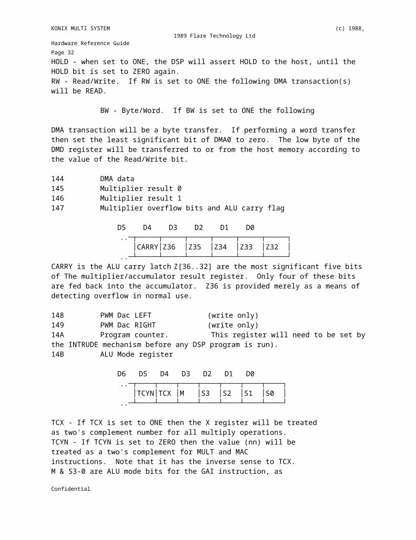
KONIX MULTI SYSTEM (c) 1988, 1989 Flare Technology LtdHardware Reference Guide Page 26 142 DMA address 0143 DMA address - top four bits, HOLD, R/W
D11 D10 D9 D3 D2 D1 D0 ..─┬────┬────┬────┬─..─┬────┬────┬────┬────┐ │HOLD│ RW │ BW │ │A19 │A18 │A17 │A16 │ ..─┴────┴────┴────┴─..─┴────┴────┴────┴────┘
HOLD - when set to ONE, the DSP will assert HOLD to the host, until the HOLD bit is set to ZERO again.RW - Read/Write. If RW is set to ONE the following DMA transaction(s) will be READ.
BW - Byte/Word. If BW is set to ONE the following
DMA transaction will be a byte transfer. If performing a word transfer then set the least significant bit of DMA0 to zero. The low byte of the DMD register will be transferred to or from the host memory according to the value of the Read/Write bit.
144 DMA data145 Multiplier result 0146 Multiplier result 1147 Multiplier overflow bits and ALU carry flag
D5 D4 D3 D2 D1 D0 ..─┬─────┬─────┬─────┬─────┬─────┬─────┐ │CARRY│Z36 │Z35 │Z34 │Z33 │Z32 │ ..─┴─────┴─────┴─────┴─────┴─────┴─────┘CARRY is the ALU carry latch Z[36..32] are the most significant five bits of The multiplier/accumulator result register. Only four of these bits are fed back into the accumulator. Z36 is provided merely as a means of detecting overflow in normal use.
148 PWM Dac LEFT (write only)149 PWM Dac RIGHT (write only)14A Program counter. This register will need to be set by the INTRUDE mechanism before any DSP program is run).14B ALU Mode register
D6 D5 D4 D3 D2 D1 D0 ..─┬────┬────┬────┬────┬────┬────┬────┐ │TCYN│TCX │M │S3 │S2 │S1 │S0 │ ..─┴────┴────┴────┴────┴────┴────┴────┘
TCX - If TCX is set to ONE then the X register will be treatedas two's complement number for all multiply operations.TCYN - If TCYN is set to ZERO then the value (nn) will be treated as a two's complement for MULT and MAC instructions. Note that it has the inverse sense to TCX.M & S3-0 are ALU mode bits for the GAI instruction, as described in the TI data book for the 74181, and in Appendix A.14C ALU X registerConfidential

KONIX MULTI SYSTEM (c) 1988, 1989 Flare Technology LtdHardware Reference Guide Page 27 14D ALU Z register (result)14E Intrude address register.14F DSP I/O pin. If this location is read then bit 0 will return the logical sense of the DSP input. If the output is enabled then the pin can be written to by the DSP (the output enable is in the video controller general purpose register).150-17F Reserved for future expansion.180-1FF 128 x 16 words of data RAM.
DSP INSTRUCTION SET
Each instruction has a 7 bit opcode and a 9 bit address vector.All micro-coded instructions (with the exception of multiply or multiply and accumulate) are completed in one 85ns cycle. All instructions are memory to register transfers or register to register transfers. Immediate values are not allowed. If a constant is needed in programming, then if it is not available in the constant table, a data RAM location must be set aside for the value.
Conditional Instructions
If bit 10 in the instruction code is SET, then the instruction is executed only if the CARRY bit in the ALU is also set.For example, if the instruction is a memory move operation the register or memory location that would be updated will remain unchanged if the carry bit is not set. Similarly if the operation is an arithmetic type, then the result register will not be updated. This is true for all instructions except MULT and MAC. It is not possible to use condition codes with these last two instructions.
Indexed Addressing
If bit 9 in the instruction code is SET, then the 9 bit address vector in the instruction code is added to the 9 bit value in the INDEX register IX, to produce the address in Data Memory operated on by the instruction.
Opcodes
MNEMONIC DESCRIPTION
00 MOV (nn), MZ0 Move data from the least significant word of the multiplier result register into data location nn.01 MOV (nn), MZ1 Move data from the most significant word of the multiplierresult register into data location nn.02MOV MZ0, (nn) Move data word from data location (nn) to least significant word of multiplier result register.03MOV MZ1, (nn) Move data word from data location nn to most significant word of multiplier result register.Confidential

KONIX MULTI SYSTEM (c) 1988, 1989 Flare Technology LtdHardware Reference Guide Page 28 04CCF Complement the carry flag05 MOV DMA0, (nn) Move data from (nn) to the least significant word of theDMA address register. Executing this instruction will start the DMA transaction in the manner described by the DMA1 register. The programmer must allow the minimum latency time to expire between two consecutive instructions of this type.06 MOV DMA1, (nn)Move data from data location (nn) to the most significant bits of the DMA address register. Control bits are also passed with this instruction. See note on DMA transfer07 MOV DMD, (nn)Move data from nn to DMA data register.08MOV (nn), DMD Move data from the DMA data register to nn.09MAC (nn) Multiply and Accumulate. Multiply the contents of nn with the contents of the X register and add the result to the number held in the multiplier result register 0A MOV MODE, (nn)Move data from location nn to the ALU mode register. This register defines:
a)The operation to be performed with the GeneralArithmetic Instruction.
b) Selection of signed or unsigned multiply operations.0B MOV IX, (nn) Move data from (nn) to the index register.0C MOV (nn), PC Move data from Program counter to nn. (useful for relative jumps, computed GOTOs etc).0DMOV X, (nn) Move data from nn to ALU X register.0EMOV (nn), X Read data from ALU X register to data location (nn).0F MULT (nn) Multiply the X register to the data in (nn).10 ADD (nn) Add the data in location (nn) to the data in the ALU X register and place the result in the ALU Z (result)register. Ignore the carry flag but change it to reflect carry from the add.11 SUB (nn)Subtract the data in nn from the data in the X register. Ignore the carry flag but change it to reflect the conditionNOT borrow.12AND (nn) Perform logical AND between data location (nn) and ALU X register.13 OR (nn)Logical OR between the data in nn and the ALU X register.14 ADC (nn)Add the data in nn, the X register and the carry bit together. Carry flag is updated.15SBC (nn) Subtract data in nn and the carry flag from the ALU X register. Carry flag is updated.16MOV (nn), AZMove the data from the ALU result register to nn.17 MOV AZ,(nn) Load the result register directly from location nn.18 MOV (nn), Z2 Load nn with the MAC overflow bits and the ALU carrybit.19 MOV DAC1, (nn)Data from nn is passed to the LEFT D to A converter.1A MOV DAC2, (nn)Data from nn is passed to the RIGHT D to A converter.1B MOV DAC12, (nn)Move data from nn to BOTH D to A converters.Confidential

KONIX MULTI SYSTEM (c) 1988, 1989 Flare Technology LtdHardware Reference Guide Page 29 1CGAI (nn) General Purpose Arithmetic Instruction. Implements theoperation defined by the code loaded into the MODEregister. See Appendix.1DMOV PC, (nn) Jump instruction. Note that because instructions arepipelined the instruction immediately following the jumpinstruction in program RAM will be executed before theone at the location specified by the contents of nn.1E NOP Guess what. Conditional version is especially useful.1F INTRUDE At least one INTRUDE instruction must be put into the dspprogram if any data transfer is to take place between hostand dsp under host control (see note).
HOST MEMORY MAP
All of the internal registers are available to the host 8086 processor. All of the internal data memory is available to the host via the INTRUDE function, although the program memory is only available to the host during the DSP STOP mode.DSP memory appears in the host address space starting at address C1000h. The addresses given below are relative to that base.
000-1FF DATA ROM - This contains a SINE table for sound generationand TRIG functions.200-27F DATA Constants - a few useful hardwired constants for use in DSP programs.280-2FF INTERNAL REGISTERS - for maximum visibility and debugging purposes, all the internal registers may be inspected by the host. They are the registers visible within the DSP data memory, with the addresses doubled.
280 Intrude data register282 Index register (9 bits are valid)284 DMA address 0286 DMA address 1 (7 bits are valid including mode bits -HOLD, R/W, B/W)288 DMA data28A Z0 MAC result register28C Z1 MAC result register28E Z2 MAC overflow & carry (6 bits valid)290 DAC Left (14 bits valid - D2 to D15, write only)292 DAC Right (14 bits valid - D2 to D15, write only)294 Program counter (8 bits are valid)296 Mode register (6 bits are valid)298 ALU X register29A ALU Z register29C Intrude address register (8 bits are valid).
Note that reading this register from the host is somewhat meaningless as it can only return its own address.Confidential

KONIX MULTI SYSTEM (c) 1988, 1989 Flare Technology LtdHardware Reference Guide Page 30 29E DSP I/O pin. (D0 is valid)
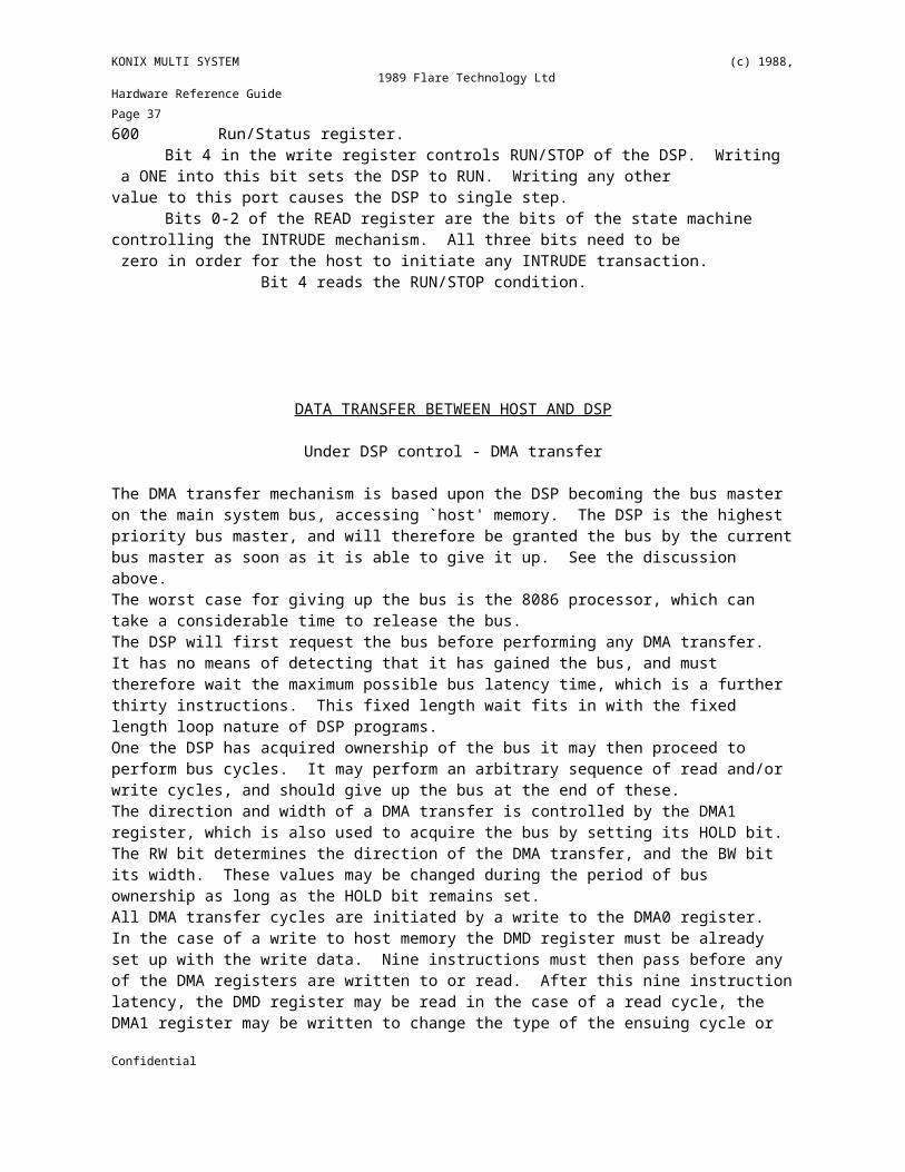
Other data bits within this register are set to zero during DSP read operations.300 - 3FF DATA RAM400 - 5FF PROGRAM RAM600 Run/Status register.
Bit 4 in the write register controls RUN/STOP of the DSP. Writing a ONE into this bit sets the DSP to RUN. Writing any other value to this port causes the DSP to single step.
Bits 0-2 of the READ register are the bits of the state machine controlling the INTRUDE mechanism. All three bits need to be zero in order for the host to initiate any INTRUDE transaction. Bit 4 reads the RUN/STOP condition.
DATA TRANSFER BETWEEN HOST AND DSP
Under DSP control - DMA transfer
The DMA transfer mechanism is based upon the DSP becoming the bus master on the main system bus, accessing `host' memory. The DSP is the highest priority bus master, and will therefore be granted the bus by the current bus master as soon as it is able to give it up. See the discussion above.The worst case for giving up the bus is the 8086 processor, which can take a considerable time to release the bus.The DSP will first request the bus before performing any DMA transfer. It has no means of detecting that it has gained the bus, and must therefore wait the maximum possible bus latency time, which is a further thirty instructions. This fixed length wait fits in with the fixed length loop nature of DSP programs.One the DSP has acquired ownership of the bus it may then proceed to perform bus cycles. It may perform an arbitrary sequence of read and/or write cycles, and should give up the bus at the end of these.The direction and width of a DMA transfer is controlled by the DMA1 register, which is also used to acquire the bus by setting its HOLD bit. The RW bit determines the direction of the DMA transfer, and the BW bit its width. These values may be changed during the period of bus ownership as long as the HOLD bit remains set.All DMA transfer cycles are initiated by a write to the DMA0 register. In the case of a write to host memory the DMD register must be already set up with the write data. Nine instructions must then pass before any of the DMA registers are written to or read. After this nine instruction latency, the DMD register may be read in the case of a read cycle, the DMA1 register may be written to change the type of the ensuing cycle or to release the bus, and DMA0 may be written to again to initiate another DMA transfer.Note that due to the bus latency period it is good practice to arrange to perform as much DMA transfer as possible within one period of bus ownership. For example, an eight-voice sample playing program should read all eight sample values in one period of bus ownership rather than Confidential

KONIX MULTI SYSTEM (c) 1988, 1989 Flare Technology LtdHardware Reference Guide Page 31 acquiring the bus independently for each. This will speed up operation of the remainder of the system, as the DSP will then own the bus for less time.The following example program fragment shows DMA transfer in operation. It takes as an example a read cycle followed by a write cycle at two separate addresses.
DATA_SEG
ADDR_HR WORD $0803 ; DMA1 for word read at 34567hADDR_LR WORD $4567 ; DMA0 for word readADDR_HW WORD $0C08 ; DMA1 for word write at 89ABChADDR_LW WORD $9ABC ; DMA0 for word writeRDATA WORD 0 ; storage for read dataWDATA WORD $3421 ; write data
CODE_SEG
...
MOV DMA1,ADDR_HR ; claim bus and set top address bits
... 30 instructions
MOV DMA0,ADDR_LR ; start read
... 9 instructions
MOV RDATA,DMD ; get data readMOV DMD,WDATA ; set up write dataMOV DMA1,ADDR_HW ; set up write operationMOV DMA0,ADDR_LW ; start write
... 9 instructions
MOV DMA1,ZERO ; release bus as write is complete
Figure - DSP DMA Example Program
Under Host Control - INTRUDE
All the internal memory is mapped into the Host 8086 address space. When the DSP is in STOP mode, the host may read and write program memory locations just as if they were normal HOST memory. When the DSP is running, however, the Program memory is not available to the host at all.DSP data memory is only available by the INTRUDE mechanism. In order that DSP operations are not disturbed in any way, data transactions can only take place when the DSP is executing INTRUDE instructions. When the DSP is stopped, it may be considered to be effectively executing INTRUDE instructions constantly.
Confidential
KONIX MULTI SYSTEM (c) 1988, 1989 Flare Technology LtdHardware Reference Guide Page 32
Host to DSP transfer
1. Ensure that the INTRUDE state machine is ready to accept new data. This is indicated by bits 0 - 2 in the status register (host location 600h) being at zero. If the DSP program length or the maximum time between INTRUDE cycles is known, then it is legitimate for the host to wait this amount of time before being sure that the DSP is ready.2. Write data to the memory location as normal
DSP to Host transfer
1. Ensure that the state machine is ready (as above).2. Read the memory location. The data read will be the data from the
last INTRUDE location and not the desired data. The action of this read is to set up the address for the INTRUDE state machine to fetch the new data from.
3. Wait for the state machine to become ready again, either by polling the intrude status or allowing a suitable delay. If intrude instructions are sufficiently closely spaced then no wait at all need be performed.
4. Read the data.
Intrude Status
The bottom three bits of the intrude status register indicate the current status of the intrude state machine. The values of interest are:
0 Idle2 Awaiting INTRUDE instruction to perform read4 Awaiting second host read of DSP to host transfer6 Awaiting INTRUDE instruction to perform write
State 4 is of particular significance. This should be checked for if there is a possibility of a single read occurring, and a dummy read performed to clear it if necessary.
Using the Blitter
Host to DSP transfer may be performed using the blitter only while the DSP is not running, into either program or data RAM. DSP to Host transfer is also possible from program RAM.However, examination of the DSP to host transfer mechanism will show that the blitter may not be used for DSP data memory to host memory transfers. DSP behaviour is not guaranteed when blitter reads are performed in the DSP data memory space, and these should not be attempted, as their behaviour cannot be relied upon.
ILLEGAL INSTRUCTION COMBINATIONS
Multiply / Multiply-Accumulate operations
These instructions take two DSP machine cycles to compute and load the result in MZ0 to MZ2. The data input to this operation is NOT pipelined so while it is possible to follow a MAC or MULT instruction with an Confidential

KONIX MULTI SYSTEM (c) 1988, 1989 Flare Technology LtdHardware Reference Guide Page 33 unrelated opcode, it is important not to immediately follow a MAC or MULT with any of the multiplier-related instructions.All of the following code combinations will generate spurious results:
BAD1: MULT (nn1)MOV X, (nn2)
This will corrupt the X register and change the result of the previous multiply
BAD2: MULT (nn1)MULT (nn2)
Whilst the result of the second multiply will be valid, it will corrupt the value of the first.
BAD3: MAC (nn2)MOV (R_X), AZ
BAD4: MAC (nn2)MOV MZ0, (nn3)
DAC instructions
Because the analogue voltage output from the DSP is achieved by producing pulses whose width is proportional to the number placed in the DACΩDAC#Ω register, it is necessary to leave a gap of at least 129 machine cycles between consecutive writes to any particular DAC register. The two registers are entirely independent and therefore can be written at any time relative to each other.Pulses are only produced when the DAC register is written to, so the effective sampling rate of the audio output is entirely under program control. The maximum sampling rate will be 93kHz and although there is no limit to the lowest sampling rate, the amplitude of the output signal will reduce in proportion to the sampling rate - i.e. the maximum output voltage is produced if the DAC register is written to every 129 machine cycles, half of maximum is produced if written to every 258 cycles, a quarter if every 516 and so on.Note also that if the sampling rate drops into the audio frequency range, then the DAC outputs will produce an audible whistle. This can be overcome by writing the same value twice, to give a higher effective sampling rate.
THE BLITTER
INTRODUCTION
This Section
This section describes the graphics co-processor, or Blitter, of the KMS system. It explains its modes of operation and how these are controlled by the programmer.Confidential

KONIX MULTI SYSTEM (c) 1988, 1989 Flare Technology LtdHardware Reference Guide Page 34 The intention of this description is to allow a competent programmer to drive the Blitter hardware directly.The Blitter is a complex device, and to drive it properly requires a pretty clear understanding of how the hardware works. This is all explained here, but a knowledge of some aspects of digital hardware design is assumed.
The Blitter
The Blitter is a co-processor of the KMS system, whose purpose is to perform graphics creation and animation as fast as possible (limited by the memory bandwidth). It can perform arbitrarily long sequences of graphics operations by reading new command sets from memory.While it is performing any graphics operations, the Blitter becomes a bus master, and denies the CPU any bus activity whatsoever. This is reasonable behaviour because the Blitter is being used to perform operations that the CPU would otherwise have performed, and is therefore speeding up program operation. This also removes the need for any asynchronous control programming for blitting operations, and the need for any interrupt generation hardware in the Blitter.However, to allow real-time programming of either of the other two processors, the Blitter will grant the bus to the DSP and Floppy Disk DMA channels, and to the CPU if an interrupt occurs. During any of these the current operation is suspended but will restart when the interrupt goes away or when the DSP DMA access completes.The Blitter may be operated in a variety of modes to perform graphics and block move operations. These are described in the sections that follow.
ARCHITECTURE
This section discusses the architecture of the Blitter, so that its modes of operation can be understood.
Overview
The internal architecture of the Blitter is best considered as three, largely separate, blocks. These are the Data Path, the Address Generator, and the Sequencer.The sequencer acts in software terms as the program that the Blitter runs, with two for loops and a couple of procedures. This program is fixed, although various parts of its operation are conditional on flags in the Blitter command, and the loop counts are also part of the command.The address generator contains three address registers. These are the program address used to fetch Blitter commands, and the source and destination address registers. It also contains an ALU with an associated step register to update addresses, and a multiplexer to generate the output address.The data path contains three data registers - the source data, destination data and pattern data registers. It also contains a versatile comparator to allow intelligent blitting operations, and a logic function unit to generate the output data.These sections are described below.
The Data PathConfidential

KONIX MULTI SYSTEM (c) 1988, 1989 Flare Technology LtdHardware Reference Guide Page 35
The Data Path contains three data registers, and two data manipulation blocks. These are the Logic Function Unit, which can combine the contents of the data registers in a number of useful ways to produce the output data; and the comparator, which can perform certain comparisons on the data to inhibit write operations, and optionally stop Blitter operation.The data path can handle data in three quanta, 16, 8 and 4 bits. Words (16 bits) are used when performing fast block moves and fills, and pixels (8 or 4 bits) may be manipulated using all the Blitter modes, such as line-drawing, multiple plane operations, character painting and so on.
│Data In │ │ ┌────────────────────┐ ├──┤Source Data Register├──────────────┬───────┐ │ └────────────────────┘ │ │ │ ┌─────────────────────────┐ │ │ ├──┤Destination Data Register├───┬─────┼─────┐ │ │ └─────────────────────────┘ │ │ │ │ │ ┌─────────────────────┐ │ │ │ │ └──┤Pattern Data Register├───────┼──┬──┼───┐ │ │ └─────────────────────┘ │ │ │ │ │ │ │ │ │ ┌┴─┴─┴─────┐ Inhibit │ │ │ │Comparator├───────── │ │ │ └──────────┘ │ │ └───────┐ │ └────────┐ │ │ ┌┴─┴┐ └─────────┐│Mux│ │└─┬─┘ ┌┴──┴───────────────┐ │Logic Function Unit│ └─┬─────────────────┘ │Data Out
Figure - Data Path
Data Path Width
The majority of the data path is eight bits wide as this is the maximum pixel size. However the source data register is sixteen bits wide, and the top 8 bits of this are used to produce the top 8 bits of the data written in sixteen bit mode, regardless of the LFU mode.
Registers
There are two eight bit wide and one sixteen bit wide data registers. These are the Pattern, Destination and Source Data registers respectively.The Source and Destination data registers are loaded from the Source andConfidential

KONIX MULTI SYSTEM (c) 1988, 1989 Flare Technology LtdHardware Reference Guide Page 36 Destination addresses in memory when the corresponding read cycles are enabled in the Inner Loop (see below). However, all three data registers are loaded at the start of Blitter operation with the pattern data, and this may be used as an additional source of data either in producing the output data or in the comparator. For example it may be a mask, a pattern for writing, a reference value, and so on. (The pattern data is loaded into both bytes of the source data register)
Logic Function Unit
The Logic Function Unit (LFU) generates the output data, which is written to the destination in memory. It can perform any logical combination of the source and destination pixels (in this case, `source' data may be selected from either of the source or pattern data registers).It does this by selecting any of the four boolean minterms Γ######## #`ì The minterms of a set of logical inputs are the set of AND terms given by each of the inputs combined together in all combinations of complimented and normal. Therefore the minterms of two inputs A and B are:
A AND B, A AND (NOT B), (NOT A) AND B and (NOT A) AND (NOT B)
Any boolean combination of A and B can be given by choosing a suitable set of minterms to OR together.Γ of the two sets of inputdata from the data registers, and generating the logical OR of the selected terms. This allows any logical combination of the of input data, there are therefore sixteen possibilities.In sixteen bit mode, the LFU will normally be set to produce source data, as it is only eight bits wide. The top eight bits written in a word write are always derived from the top 8 bits of the source data register.
Comparator
The comparator can perform a variety of comparisons on the data in the source, destination and pattern data registers. If its comparison conditions are met then it generates an inhibit signal. This is used to inhibit a write operation, and optionally to stop blitting operation.The comparator may be used to provide a pixel plane effect, to give transparent colours, for collision detection and memory search operations, and as an aid to character painting.
Comparator Pixel Plane Operation
Multiple plane operation is supported by assigning a plane number to every pixel. In eight-bit pixel mode two of the eight bits are used giving two or four planes, in four-bit pixel mode one of the four bits is used giving two planes.
The bits are allocated within the byte thus:
Bit│ Plane Function │8 bit pixel│4 bit pixel
Confidential
KONIX MULTI SYSTEM (c) 1988, 1989 Flare Technology LtdHardware Reference Guide Page 37 ───┼───────────┼─────────── 0 │ │ ───┼───────────┼─────────── 1 │ │ ───┼───────────┼─────────── 2 │ │ ───┼───────────┼─────────── 3 │ │ Plane bit ───┼───────────┼─────────── 4 │ │ ───┼───────────┼─────────── 5 │ │ ───┼───────────┼─────────── 6 │Plane bit 0│ ───┼───────────┼─────────── 7 │Plane bit 1│ Plane bit
The comparator can produce an inhibit output if the plane number of the destination data is equal to, not equal to, or greater than the plane number of the source data, or any combination of these. This means that data being written onto the screen can be masked by data already present in a different plane.
Comparator Pixel Value Comparison
The comparator can produce an inhibit output if the entire source pixel is equal to or not equal to the destination byte. This may be used, for example, for searching memory for a particular value; and, more importantly, for designating a colour to be transparent, and holding the transparent colour value in a data register.
Comparator Bit to Byte Expansion
This comparator operation allows bit to pixel expansion of data, used for example for character painting. In this mode the comparator selects a bit of the source byte based on the value of the inner counter (refer to the Sequencer Description), and inhibits the write operation if this bit is zero.
Handling of Data in Four and Eight Bit Pixel Modes
The Blitter makes provision for handling two screen pixel resolution modes. These are eight bit mode, where each byte corresponds to one pixel, and four bit mode, where each byte corresponds to two pixels.In eight bit pixel mode the data path is handling one pixel at a time, and this makes its operation straightforward. In four pixel bit mode, however, only half of the byte that is read from or written to is the current pixel so certain additional requirements are placed on the data path.In a four bit mode write operation unchanged destination data is written to the half of the data byte that does not correspond to the current pixel. This means that write-only Blitter operation will not work properly in this mode, so that control bit DSTEN must always be set.Confidential

KONIX MULTI SYSTEM (c) 1988, 1989 Flare Technology LtdHardware Reference Guide Page 38 It is also possible that the source four bit pixel address and the destination four bit pixel address point at different halves of the corresponding bytes of RAM. If this is the case, a shifter swaps the two halves of the source data.
This is all handled transparently to the user. However certain caveats should be noted:
1. In four bit mode, destination reads must always be performed. If this is not done then the pixel in the other half of the destination byte will be corrupted.
2. In four bit mode, the two nibbles of the pattern byte should normally be set to the same value.
Note, however, that the Blitter may be set to eight bit mode when the display is in four bit mode, to perform operations in two pixel multiples, and this will speed up certain operations (but not as much as word mode where this is applicable).
The Address Generator
The address generator contains three address registers, an increment or step register, an address adder, and an address output multiplexer.
┌──────┐ │ ┌────┴───────────────────┐ │ │Program Address Register│ │ └─────────────────┬──────┘ ├──────┐ └────────────────┬─────────────────┐ │ ┌────┴──────────────────┐ │ │ │ │Source Address Register│ │ │ │ └─────────────────┬─────┘ │ │ ├──────┐ └──────────────┐ │ │ │ ┌────┴───────────────────────┐ │ │ │Confidential

KONIX MULTI SYSTEM (c) 1988, 1989 Flare Technology LtdHardware Reference Guide Page 39 │ │Destination Address Register│ │ │ │ │ └─────────────────┬──────────┘ ├─┼─────────────┐ │ │ └────────────┬─┼─┼────────┐ │ │ │ │ │ │ ┌────┴────┴───┴────┐ │ │ │ │ │Address Output Mux│ │ │ │ │ └─────────┬────────┘ │ │ │ │ └───────Address │ │ │ │ ┌─────────────┐ │ │ │ │ │Step Register│ │ │ │ │ └───────┬─────┘ │ ┌┴─┴─┴┐ ┌───────┴──────┐ │ │ Mux │ │Update Control│ │ └──┬──┘ └───────┬──────┘ │ ┌──┴───────────────────┴─┐ │ │ Adder │ │ └───────────┬────────────┘ └───────────────────────────────────────────┘
Figure - Address Generator
The Address Registers
There are three address registers holding the source address, the destination address, and the program address.Each of these registers contains twenty address bits, referred to as bits 0 to 19, allowing the Blitter to address up to One Megabyte. In addition to this the source and destination address registers contain a nibble bit used in four-bit pixel mode, designated bit -1.The Program address register holds the address that the program is fetched from, and is incremented by one each time a memory cycle is performed using it.The Source and Destination Address registers are updated after each cycle, and at other times, using an adder that allows them considerable flexibility in the objects to which they refer.All source and destination address updating may be performed optionally on just the bottom sixteen bits of the address register. This means that the Blitter will then effectively operate in 64K pages. In this mode if an address overflows in a page, it will wrap, and the overflow (or underflow) will be lost.
The Address Adder
The address adder is a twenty-one bit wide adder used to update addresses. It allows either a constant value of 0.5, 1 or 2, or a variable stored in the step register, to be added to an address value. It can also subtract the same values. The twenty-first bit is the nibble part of the address.Note that an increment of one pixel has a different effect on the address depending on the screen resolution set, and that this is automatically catered for.All address registers are updated automatically at the end of the appropriate memory cycles, source read for the source address register,
Confidential

KONIX MULTI SYSTEM (c) 1988, 1989 Flare Technology LtdHardware Reference Guide Page 40 and destination write (even if inhibited) for the destination address register.
The Address Output Multiplexer
The address output multiplexer provides the external address to the system memory. It provides three types of address, these are the Source Address, the Destination Address and the Program Address. These are derived directly from the corresponding address registers.
Line Drawing Address
When a line draw is being performed, the address registers are used in a different way from normal. The Destination Address register is used as the line draw address, and the Source Address register and Step register are used as Delta One and Delta Two respectively. During line drawing Delta Two is subtracted from Delta One, and the borrow output produced is used to determine what is added to the Destination Address register. See the section on line-draw below.
The Sequencer
The sequencer and controller section controls the operation of the other sections of the Blitter, and therefore governs the overall operation of the device.The flow of control is best considered at two main levels. There is an outer loop governing the overall flow of control, and within that three subsections, the inner loop, the parameter read procedure and the command read procedure.
┌────────────┐ │ Outer Loop │ └┬────┬─────┬┘ ┌───────────────┘ │ └─────────────┐ ┌──────┴───────┐ ┌───────┴────────┐ ┌─────┴──────┐ │ Command Read │ │ Parameter Read │ │ Inner Loop │ └──────────────┘ └────────────────┘ └────────────┘
Figure - Control hierarchy
This might also be viewed as a simple program, e.g.
read_command()for n=0 to outer_count
read_parameters()for m=0 to inner_count
if SRCEN then read_source()if DSTEN then read_destination()
Confidential
KONIX MULTI SYSTEM (c) 1988, 1989 Flare Technology LtdHardware Reference Guide Page 41
write_destination()next m
next n
(This ignores a lot of the Blitter control bits)
The blocks in the diagram above represent state machines within the Blitter, and various control bits within the Blitter command affect their operation. To set these control bits correctly requires some understanding of the flow of control within the Blitter, and this is discussed below.
The Inner Loop
The inner loop performs the actual blitting or line-drawing operation.
┌───────┐ │ Entry │ └───┬───┘ │ ┌──────────────────┐ ┌────┴──┴──┐ │ │SRCEN set?├─────────┐ │ └────┬─────┘N │ │ │Y │ │ ╔═════════╧══════╗ │ │ ║Read Source Data║ │ │ ╚═════════╤══════╝ │ │ ╔═════════╧═══════════╗ │ │ ║Update Source Address║ │ │ ╚═════════╤═══════════╝ │ │ │ ┌────────────┘ │ ┌────┴──┴──┐ │Confidential

KONIX MULTI SYSTEM (c) 1988, 1989 Flare Technology LtdHardware Reference Guide Page 42 │DSTEN set?├─────────┐ │ └────┬─────┘N │ │ │Y │ │ ╔═════════╧═══════════╗ │ │ ║Read Destination Data║ │ │ ╚═════════╤═══════════╝ │ │ │ ┌────────────┘ │ ┌────┴──┴──────┐ │ │Inhibit write?├───────────┼──────────┐ └────┬─────────┘Y │ │ │N │ │ ╔═════════╧════════════╗ │ ┌───────┴───────┐ ║Write Destination Data║ │ │Collision stop?│ ╚═════════╤════════════╝ │ └───┬───────┬───┘ │ ┌──────────────────┼──────┘N │Y │ │ │ ╔══════╧══════════╗ │ │ ┌───────────────┼───────╢Suspend operation║ ╔═════════╧══╧══╧══════════╗ │ resume╚══════╤══════════╝ ║Update Destination Address║ │ │reset ╚═════════╤════════════════╝ │ │ ╔═════════╧═════════════╗ │ │ ║Decrement Inner Counter║ │ │ ╚═════════╤═════════════╝ │ │ ┌────┴────────────────┐ │ │ │Counter reached zero?├────┘ │ └────┬────────────────┘N │ │Y ┌───────────────────────────────┘ ┌─────────┴────┴─────┐ │Exit from Inner Loop│ └────────────────────┘
Figure - Blitter Inner Loop Flow Diagram
An Inner Loop cycle can contain up to three memory cycles. These are a read from the source address, a read from the destination address, and a write to the destination address. All three cycles are optional.
If the loop type includes a source read, or a source read and a destination read, then the comparator inhibit mechanism is tested before the destination write occurs. This allows the write cycles to be bypassed when the comparator inhibit conditions are met.Under these circumstances it is possible to have the current operation cease and control returned to the CPU. The program may then examine the address registers to determine where the inhibit has occurred, so that collision detection may be performed; and may determine whether to resume operation or abort it.The Inner Loop is repeated until the inner counter reaches zero. This is an nine bit counter, and so can be any number of times from 1 to 512.
Collision Detection
Confidential

KONIX MULTI SYSTEM (c) 1988, 1989 Flare Technology LtdHardware Reference Guide Page 43 As can be seen in the diagram above, the Blitter makes provision for collision detection by allowing operation to stop when a comparator write inhibit occurs. When this happens, control returns to the CPU, which may then examine the internal state of the Blitter to determine what has caused the collision.At this point, the CPU may choose to allow the Blitter to resume the operation it was performing, or may reset it back to its idle state. Either a reset or a resume command must be issued before the Blitter may be used for another operation.Note that while the Blitter is in this suspended state a new value may be written to the command register, so that the collision stop mechanism may be disabled.
Inner Loop Execution Times
Normally the inner loop will execute at a rate determined only by the cycle time of the memory being accessed, with no gaps between memory cycles. The only exception to this is an inhibited write cycle, in which case two 12 MHz ticks are required for destination address updating.
The Parameter Read Procedure
The parameter read procedure is a very straightforward sequence that loads up a new set of parameters to the inner loop.It reads, in sequence, the inner loop counter value, the step register value, and the pattern value - used to preset the data registers.The inner count is the number of times the Inner Loop is repeated; the step register is used for address incrementing, and the pattern is used for data manipulation.This procedure is called as part of the command read operation at the start of a Blitter operation; and is also called if required during a blitting operation (the PARRD control bit determines this). These extra parameter reads occur between passes through the Inner Loop, to allow various parameters of the loop to be altered. This allows such operations as irregular shape painting and run-length encoded data expansion.
The Command Read Procedure
The command read procedure is used to start a new blitting operation. The inactive, reset state of the Blitter is part of this procedure. It looks like this:
Enter ┌────┴────────────┐ │Read Command Word│ └────┬────────────┘ ┌────┴──────────┐ │RUN status set?├─┐no └────┬──────────┘ │ │yes ╔═╧═════════════╗ │ ║Blitter stopped║ │ ╚═╤═════════════╝Confidential

KONIX MULTI SYSTEM (c) 1988, 1989 Flare Technology LtdHardware Reference Guide Page 44 │ │start ┌────┴────────────┴───────────┐ │Read Source Address Low Word │ └────┬────────────────────────┘ ┌────┴────────────────────────┐ │Read Source Address High Word│ └────┬────────────────────────┘ ┌────┴─────────────────────────────┐ │Read Destination Address Low Word │ └────┬─────────────────────────────┘ ┌────┴─────────────────────────────┐ │Read Destination Address High Word│ └────┬─────────────────────────────┘ Exit
Figure - Blitter Command Read Loop Flow Diagram
The Stopped state of the Command read loop represents the normal inactive state of the Blitter. From this state a Command register I/O write is performed to start the Blitter, usually preceded by a write of the program address register.The full set of operational parameters is loaded from the program count address, which is auto-incremented, and control passes out of the command read loop.When a blitting operation is completed, a new command is read from the program count address, and if this command leaves the Blitter in Run mode, then a new set of parameters is loaded and another operation is started. Otherwise the Blitter enters its Stopped state and returns the bus to the CPU.This mechanism allows the Blitter to perform arbitrarily long sequences of graphics commands without requiring any processor intervention. This is extremely useful, as processor I/O write cycles are relatively slow in comparison to Blitter memory reads.
The Outer Loop
The Outer Loop controls the overall operation of the Blitter, including starting off the three inner loops described above. Its flow of control looks like this:
┌───────────────────────┐ ╔═╧══════════╗ │ ║LOAD COMMAND║ │ ╚═╤══════════╝ │ │ ┌────────────────┼────┐ ╔═╧══════╧══════╗ │ │ ║LOAD PARAMETERS║ │ │ ╚═╤═════════════╝ │ │ │ ┌────────────────┼────┼────┐ ╔═╧══════╧═╗ │ │ │ ║INNER LOOP║ │ │ │ ╚═╤════════╝ │ │ │Confidential

KONIX MULTI SYSTEM (c) 1988, 1989 Flare Technology LtdHardware Reference Guide Page 45 ┌─┴───────────────────┐ │ │ │ │Decrement outer count│ │ │ │ └─┬───────────────────┘ │ │ │ ┌─┴───────────────┐yes │ │ │ │Outer count zero?├───────┘ │ │ └─┬───────────────┘ │ │ │no │ │ ┌─┴─────────────┐ │ │ │DSTUP flag set?│ │ │ └─┬───┬─────────┘ │ │ │no │yes │ │ │ ┌─┴────────────────┐ │ │ │ │Update destination│ │ │ │ └─┬────────────────┘ │ │ ┌─┴───┴─────────┐ │ │ │SRCUP flag set?│ │ │ └─┬───┬─────────┘ │ │ │no │yes │ │ │ ┌─┴───────────┐ │ │ │ │Update source│ │ │ │ └─┬───────────┘ │ │ ┌─┴───┴─────────┐yes │ │ │PARRD flag set?├──────────────┘ │ └──────┬────────┘ │ no└────────────────────────────┘
Figure - Outer Loop Flow Diagram
Normal operation starts on exit from the command read loop. The parameter read loop then entered to read the first set of parameters, and then the inner loop is entered, with the inner counter being loaded ti its initial value before the start of operation.The Outer counter is then decremented, and if it is zero, then the command read loop is entered; then either or both of the source address and destination address register may be updated with the contents of the step register. The parameter read loop may then be optionally entered to update various inner loop parameters, before the inner loop is entered again.The two loops allow the Blitter it to cope with two-dimensional screen structures, with the outer loop address register updates moving screen address pointers onto the start of the structure on the next line. The parameter read loop adds flexibility by allowing the screen structure parameters to be altered on a line by line basis.
Memory Interface and Interrupts
All the memory cycles are controlled by a memory interface state machine. This controls the cycle timing generation, and the bus arbitration.The blitter will take over the bus from the 8086 for the duration of a blitter command sequence. This is subject to the bus handover latency discussed above, but as soon as the blitter is granted the bus its operation will start.
Confidential

KONIX MULTI SYSTEM (c) 1988, 1989 Flare Technology LtdHardware Reference Guide Page 46 The memory interface will give up the bus to the DSP or the floppy disk read channel as soon as one of these requests the bus, pausing only to complete any current memory cycle.Interrupts will also cause the blitter to suspend operation, unless masked in the blitter control register. The blitter detects the state of the interrupt line itself, and uses this to suspend operation. Operation will resume as soon as the interrupt line is cleared, which occurs when the 8086 OUT to the ACK port occurs. As this may not necessarily be the end of the interrupt service routine, programmers should be wary of stack crawl, and should normally keep interrupts disabled during a service routine.The blitter will resume operation as soon as the interrupt line is cleared without any intervention from the 8086 processor.Note that the blitter only responds to the internal interrupt sources, i.e. the video, analogue inputs, and floppy disk interrupts. Any external interrupt source will have no effect on the blitter.
MODES OF OPERATION
This section describes some of the modes of operation of the Blitter, and how they should be programmed. An understanding of the previous section describing the mechanisms of the Blitter is assumed.
Simple Memory Fill and Copy Operations
The simplest operations are those involving copying one block of memory to another, and filling a block of memory with a pre-defined value. These operations can be performed on linear parts of memory, and on arbitrary screen rectangles.The destination data register is used as the address of the memory being modified, and the source address register is used as the address of the data being copied, if it is a copy operation.
Handling of Data
The output data being given by the Logic Function Unit will be selected as Pattern data in the case of a memory fill, or as Source data in the case of a memory copy. For simple operations, the comparator control register will be set to zero.
Addressing and Counters
When the operation is to be performed on linear areas of memory, most of the address control bits will be set to zero. The step register is not used, and the only requirement is to determine whether the copy will be made with the address incrementing or decrementing, and setting DSIGN and SSIGN appropriately. Note that the initial value placed in the address register should be the bottom of the area to be operated on if the sign bit is not set, and at the top if it is. In both cases, the first byte read or written will be the first address. The length of the operation will be placed in the inner counter, and the outer counter set to one.
Confidential
KONIX MULTI SYSTEM (c) 1988, 1989 Flare Technology LtdHardware Reference Guide Page 47 If the block being operated on is very large, then the inner and outer counters may both have to be used, and the number of bytes operated on will be given by the product of the inner and outer counter values.When either or both of the source and destination data are rectangles rather than linear areas, then the inner counter will contain the rectangle width, and the outer counter the rectangle height. The step register is set to the address increment from the right hand side of the rectangle round to the left hand side on the next line. The SRCUP and DSTUP bits are set according to whether the source or destination are rectangles.
Inner loop mode control
In eight-bit pixel mode, neither SRCEN nor DSTEN will be used for memory fill, bit SRCEN should be set for memory copy. In four-bit pixel mode DSTEN must always be set as well, so that a destination read is performed to avoid corrupting the other pixel. Note that this will be slower.
Line Drawing
Line drawing is based on a simple D.D.A.(Digital Differential Analyzer) algorithm. The basis of this is that for a given line one of the X-address or Y-address is always incremented for every pixel drawn, while the other one is incremented if a suitable arithmetic condition is met. This produces a line like this:
┌───┬───┬───┬───┬───┬───┐ │ │ │ │ │ │ │ ├───┼───┼───┼───┼───┼───┤ │ │ │ │ │███│███│ ├───┼───┼───┼───┼───┼───┤ │ │ │███│███│ │ │ ├───┼───┼───┼───┼───┼───┤ │███│███│ │ │ │ │ └───┴───┴───┴───┴───┴───┘ │ └─────── after this pixel, both X and Y are incremented └─────────── after this pixel, only X is incremented
The algorithm used by the Blitter computes the arithmetic condition that causes the conditional increment by repeated subtraction of the smaller of ≥#≥#dx≥#≥# or ≥#≥#dy≥#≥#Γ######## #`ì The notation ≥#≥#dx≥#≥# refers to the distance along the X-axis that the line corresponds to. This is given by ≥#≥#|(x1 - x2)|≥#≥# where ≥#≥#x1≥#≥# and ≥#≥#x2≥#≥# are the X-coordinates of the end points - the vertical bar notation means the magnitude or modulus of their difference. Γ from a working value, with the larger being added back when underflow occurs ? effectively division to give the gradient.
Computation of line-draw arguments
If a line is being drawn from ≥#≥#(x1,y1)≥#≥# to ≥#≥#(x2,y2)≥#≥#, then:Confidential

KONIX MULTI SYSTEM (c) 1988, 1989 Flare Technology LtdHardware Reference Guide Page 48
≥#≥#dx = |(x1-x2)|≥#≥#≥#≥#dy = |(y1-y2)|≥#≥#
From these ≥#≥#d1≥#≥# is given by the larger of ≥#≥#dx≥#≥# and ≥#≥#dy≥#≥#, ≥#≥#d2≥#≥# by the smaller. Then, for each pixel drawn, ≥#≥#d2≥#≥# is subtracted from a working value, which is initially set to≥#≥#d1/2≥#≥#, and the sign of the result of this subtraction (indicating underflow) is the arithmetic condition for the conditional part of the screen address update. When this underflow occurs, the original value of ≥#≥#d1≥#≥# is added back to the working value.It can be seen that the ratio of ≥#≥#dx≥#≥# to ≥#≥#dy≥#≥# will give the frequency with which this underflow and adding-back occurs. The ratio between them is, of course, also the gradient of the line (Q.E.D!).
Creating a line draw Blitter command
These values are used to set the Blitter command as follows:The start point of the line ≥#≥#(x1,y1)≥#≥# is the destination address≥#≥#d1≥#≥# is placed in the middle byte of the source address register - this is the stored original value, and ≥#≥#d1/2≥#≥# is placed in the low byte - this is the working value.≥#≥#d1≥#≥# also gives the inner counter value, although ≥#≥#d1+1≥#≥# should be used if both end points of the line are to be drawn. î≥#≥#d2≥#≥# is placed in the step register.If ≥#≥#dx > dy≥#≥# then the YFRAC flag is set, otherwise it is cleared.SSIGN gives the sign of X-address updates, DSIGN the sign of Y-address updates.In low and medium resolution modes ≥#≥#d1≥#≥# and ≥#≥#d2≥#≥# are eight-bit values. However, in high-resolution mode it is be necessary to extend them to nine-bit values to get the necessary resolution of line-position. In this case, a further, less-significant, bit is used which would otherwise be set to zero. This is the so-called `minus one' bit.The inner counter value, given by ≥#≥#d1≥#≥#, is also a nine-bit value, but in this case the most significant bit is placed in ILCNT8, and the lower eight bits in the inner counter byte.The least significant bit of ≥#≥#d2≥#≥# is placed in STEP-1, the least significant bit of the add-back value is placed in Source Address bit 16, and the least significant bit of the working value is placed in Source Address bit -1.Note that as ≥#≥#dy≥#≥# is never more than 256, ≥#≥#d2≥#≥# is similarly restricted, so that in high-resolution mode its top bit (of nine) is always clear.
Handling of Data
As all the registers in the address section are occupied in computing the line address, the Blitter has no ability to move data from somewhere else when drawing lines. Therefore the data written at the line address has to be given either directly by the pattern data or by a combination of the pattern register and the data already there, according to the L.F.U.The implication of this is that SRCEN should not be set, for it would produce random data!
Addressing and CountersConfidential

KONIX MULTI SYSTEM (c) 1988, 1989 Flare Technology LtdHardware Reference Guide Page 49
The addressing has largely been discussed above. The inner counter is set to the length of the line, and the outer counter will be set to one.
Mode control
In eight-bit pixel mode, DSTEN need not be set, unless used for read-modify-write operation. In four-bit pixel mode, DSTEN must always be set, so that a destination read is performed to avoid corrupting the other pixel.
Example Program
This program fragment demonstrates a Blitter program to draw a line from 21,133 to 97,27 on a medium res screen (considering the origin to be at the top left).These figures give ≥#≥#dx≥#≥# = 76 and ≥#≥#dy≥#≥# = -106. Therefore ≥#≥#d1≥#≥# = 106 and ≥#≥#d2≥#≥# = 76. YFRAC is clear, and DSIGN is set to make Y updates negative.
mov ax,offset bprogout (BLPROG),axmov ax,0102h ; assume cs is 2000hout (BLCMD),ax
....
EVEN ; force onto word boundarybprog:
DB 53 ; half d1 is working valueDB 106 ; d1 for add-backDB 0 ; source address high byteDB 1 ; outer loop valueDB 21,133 ; start pixel is destination addressDB 040h ; assume screen at 00000h, set DSIGNDB 0C0h ; write source data, comparator offDB 107 ; inner count=d1+1 to draw both endsDB 00101000b ; set medium res, and LINDRDB 033h ; pattern value gives line colourDB 76 ; d2 is step valueDW 0 ; command of 0 at end stops Blitter
Character Painting
The Blitter has the ability to paint characters on the screen as a single operation. Character painting as far as the Blitter is concerned involves painting a rectangular area up to 8 pixels wide and of arbitrary height. The pixels in this area are either written to or left unchanged according to a bit pattern.This mode of use is not restricted to character painting, but may be used for expanding any graphics stored as a monochrome bit plane.Confidential

KONIX MULTI SYSTEM (c) 1988, 1989 Flare Technology LtdHardware Reference Guide Page 50
Character Font
The source register addresses the bit pattern, normally part of the font, where each byte corresponds to one row of the character. Therefore Blitter fonts may be up to 8 pixels wide. Wider fonts may of course be used, but these will require more than one Blitter operation to paint a character.
The data is arranged with the bit corresponding to the left-most pixel in the least significant bit, and the top of a character at the lowest address. If the data is less than 8 pixels wide, then the least significant bits of the font data are not used.
For example, the font entry for the letter R in a 6x10 font would be something like this:
Byte Pixels set Binary Hex─────────┬─────┬───────────────────0 │xxxx │ 01111000 781 │x x│ 10001000 882 │x x│ 10001000 883 │x x │ 01001000 484 │xxx │ 00111000 385 │x x │ 00101000 286 │x x │ 01001000 487 │x x│ 10001000 888 │x x│ 10001000 889 │ │ 00000000 00─────────┴─────┴───────────────────
Mode Control and Screen Addressing
The destination address register is used to address the area of the screen to which the character is to be painted. Normally this area will have been cleared to the required background colour by a previous Blitter operation. The destination address is initialised to the top left hand corner of the character.The character to be painted is a rectangle, and therefore the destination addressing is programmed correspondingly. The Inner Counter is set to the width of the character and the Outer Counter to its height. The step register is set to be the screen width less the width of the character. The DSTUP bit is set to allow the destination address to be updated between passes through the inner loop.Inner loop control bits DSTEN and SRCENF are set, character painting being the reason for the existence of SRCENF. This allows the font byte for each row to be read just once.The comparator is used to control the painting of pixels, and so the CMPBIT control bit is set, to enable its bit to byte expansion mechanism.
Confidential
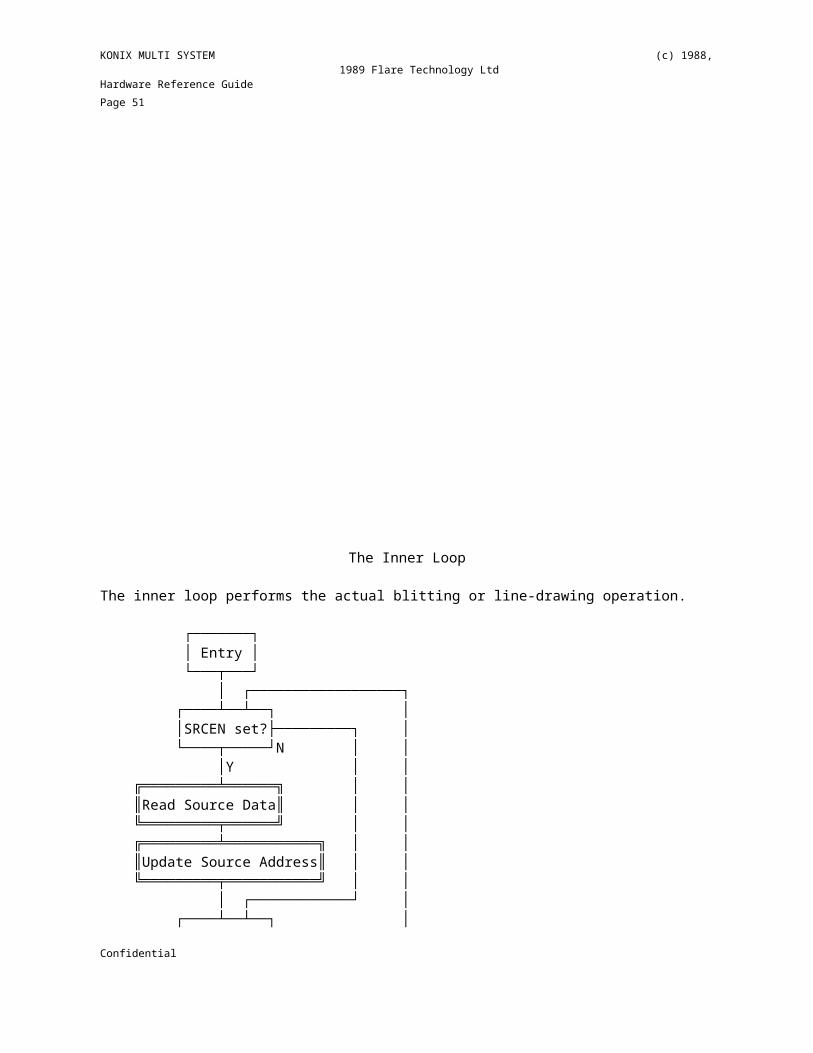
KONIX MULTI SYSTEM (c) 1988, 1989 Flare Technology LtdHardware Reference Guide Page 51
Handling of data in character paint
The colour to be painted is set as the pattern, and this will normally be held in the pattern data register. In four-bit pixel mode, DSTEN will be set, and the destination data register will hold the read value so that the other half of the byte may be written back undisturbed. The source data register holds the font pattern, as mentioned above.
BLITTER COMMAND FORMAT
A Blitter command is given as a table of data in memory. The Blitter loads the contents of this table into its internal registers and performs the specified operation. The Blitter will read successive sets of commands until a stop instruction is read into the command register.The Blitter program address must be set up before the command word is issued. The Blitter program address is given by the program address register, which is hold the low 16-bits of the address, and the command register, which contains the top four bits of the address. The program must lie on a word boundary.A full table of Blitter command data starts with a command word. However the first Blitter command in a sequence has its command word written into the command register by a CPU I/O cycleΓ######## #`ì Note that the program address top nibble field is only updated by I/O writes, and is not affected by blitter program fetches of this word. Γ, and so starts reading the command data from the second word (Word 1); and similarly the last Blitter command need consist of no more than a command word with the RUN bit clear. A Blitter command takes the form (in the order low byte, high byte):
7 6 5 4 3 2 1 0 ┌──────┬──────┬──────┬──────┬───────────────────────────┐ Word 0 │ENSTP8│ENSTPS│ENSTEP│ │Program address top nibble │ ├──────┼──────┼──────┼──────┼──────┬──────┬──────┬──────┤ │SRCENF│DSTEN │SRCEN │DSTUP │SRCUP │PARRD │COLST │RUN │ ├──────┴──────┴──────┴──────┴──────┴──────┴──────┴──────┤ Word 1 │ ---- Source address byte 0 ---- │ ├───────────────────────────────────────────────────────┤ │ ---- Source address byte 1 ---- │ ├──────┬──────┬──────┬──────┬───────────────────────────┤ Word 2 │SRCA-1│SSIGN │SWRAP │SRCCMP│ Source address top nibble │ ├──────┴──────┴──────┴──────┴───────────────────────────┤ │ ---- Outer loop counter value ---- │ ├───────────────────────────────────────────────────────┤ Word 3 │ ---- Destination address byte 0 ---- │ ├───────────────────────────────────────────────────────┤ │ ---- Destination address byte 1 ---- │ ├──────┬──────┬──────┬──────┬───────────────────────────┤ Word 4 │DSTA-1│DSIGN │DWRAP │DSTCMP│Destination addr top nibble│ ├──────┼──────┼──────┼──────┼──────┬──────┬──────┬──────┤ │LFU3 │LFU2 │LFU1 │LFU0 │CMPPLN│CMPGT │CMPNE │CMPEQ │ ├──────┴──────┴──────┴──────┴──────┴──────┴──────┴──────┤ Word 5 │ ---- Inner loop counter value (1-512) ---- │ ├──────┬──────┬──────┬──────┬──────┬──────┬──────┬──────┤Confidential

KONIX MULTI SYSTEM (c) 1988, 1989 Flare Technology LtdHardware Reference Guide Page 52 │PATSEL│RES1 │RES0 │YFRAC │LINDR │CMPBIT│STEP-1│ILCNT8│ ├──────┴──────┴──────┴──────┴──────┴──────┴──────┴──────┤ Word 6 │ ---- Pattern byte ---- │ ├───────────────────────────────────────────────────────┤ │ ---- Step register ---- │ └───────────────────────────────────────────────────────┘
Figure - Blitter command summary
Command and Mode Control Bits
RUN causes the Blitter to start operation. It is used when writing to the command register as an I/O port to start the Blitter reading a command. If the Blitter loads a command with RUN set to zero, as part of a command read, then operation ceases.
COLST causes operation to stop if a collision (write inhibit) occurs. From this point the current operation can be resumed or aborted, and various internal registers may be read. (See comparator control bits).
PARRD requires the Blitter to read a new parameter set (that is the inner count and mode bits, and the pattern register and step value) from the program counter address, every time the inner loop exits and the outer count has not reached zero.
SRCUP requires the contents of the step register to be added to the source address on exit from the inner loop if the outer count has not reached zero.
DSTUP requires the contents of the step register to be added to the destination address on exit from the inner loop if the outer count has not reached zero.
SRCEN enables a source address read in the inner loop. This will also cause the source address register to be incremented according to the pixel size.
DSTEN enables a destination address read in the inner loop. This does not affect the destination address register which is incremented as part of the destination write cycle.
SRCENF is a special case of SRCEN and causes the source address to be read when the inner loop is first entered, but not subsequently. This is relevant to character paint mode. SRCENF has no effect if SRCEN is set.
ILCNT 0-8 are the inner loop counter initial value. This is loaded into the inner loop counter every time the inner loop is entered. Note that setting the inner count low byte to zero will produce 512 operations unless the top bit is set.
LINDR sets line-drawing mode. This mode uses both the source and destination address registers to generate the line-draw address, which may be used for both reading and writing.Confidential

KONIX MULTI SYSTEM (c) 1988, 1989 Flare Technology LtdHardware Reference Guide Page 53
YFRAC indicates which of the X and Y addresses has the fractional increment in line-drawing mode. It is set if the Y address has the fractional increment.
RES0 and RES1 give the screen mode used by Blitter operations. The screen modes are as follows:
RES1 RES0 Word size Screen width0 0 4 bits 256 pixels0 1 8 bits 256 pixels1 0 4 bits 512 pixels1 1 16 bits n/a
Note that the screen width given is only relevant to line-drawing mode, and that 16 bit mode may not be used in line drawing mode.
PATSEL is used to select the pattern data register to replace the source data register as the source input to the LFU. This is relevant to character painting, where the source data register will contain the font data, and the pattern data register will contain the ink colour.
Step Register and Enhanced Step Control Bits
STEP 0-7 are the eight most significant bits of the step. The step is used to increment an address by a number other then 1, so that non-contiguous screen data may be handled in single operations. The step register is also used in line drawing mode to hold d2.
STEP -1 is the least significant bit of the step. It is used a the nibble bit of the step when in high resolution mode.
ENSTEP enables the enhanced step register functions. These allows the step register to update an address register with two enhancements over the normal function, controlled by the two bits below.
ENSTP8 is an additional more significant step bit so that values greater than 256 may be added to the address register.
ENSTPS gives the sign of the step update. This overrides the setting of the address update sign bit for any step add operations.
Comparator Control Bits
CMPPLN enables plane mode where the three comparator functions operate on the plane number bits as opposed to the entire pixel.
CMPEQ causes the comparator to inhibit an inner loop write, if in plane mode the priority of the destination pixel is equal to the plane priority of the source pixel, or if the entire pixel is the same if not in plane mode.
CMPNE causes the comparator to inhibit an inner loop write, if in plane mode the priority of the destination pixel is not equal to the plane Confidential

KONIX MULTI SYSTEM (c) 1988, 1989 Flare Technology LtdHardware Reference Guide Page 54 priority of the source pixel, or if the entire pixel is not the same if not in plane mode.
CMPGT only operates in plane mode, and causes the comparator to inhibit the write if the plane priority of the destination pixel is greater than the plane priority of the source pixel.
CMPBIT is used to give a bit to byte expansion scheme. It causes the comparator to generate an inhibit by selecting a bit of the source data register using the inner counter, and generating an inhibit if the bit selected is a zero. The selection is given by 8 in the inner counter selecting bit 0, 7 selecting bit 1, 6 bit 2, and so on.
Logic Function Unit Control Bits
LFU 0-3 The logic function unit (L.F.U.) controls the data that is written in a destination write cycle. The L.F.U. allows any logical combination of the source and destination data. This is achieved by each of the L.F.U. bits selecting one of the Minterms, with the output being given by the OR of the selected terms.
The correspondence between bits and Minterms is
LOG0 NOT source AND NOT destinationLOG1 NOT source AND destinationLOG2 source AND NOT destinationLOG3 source AND destination
There are therefore sixteen possibilities.
Source Address Register and Control Bits
The Source Address Register is used as a pointer to a source of data for blitting operations. Bits SRCA0 to SRCA19 correspond directly to address lines 0 to 19. The SRCA-1 bit is used as a nibble address in high resolution mode.The source address register is also used as d1 and as the division workspace in line-drawing mode. Refer to the description of line-drawing mode.
SWRAP causes source address updates to wrap on 64K boundaries, as opposed to running linearly through memory.
SSIGN is the sign used when updating the source address. Setting it causes the source address to be decremented rather then rather then incremented. It makes X negative in line-drawing.
SRCCMP selects the source data register as the source input to the comparator. If it is clear, the pattern data register is used.
Destination Address Register and Control Bits
Confidential

KONIX MULTI SYSTEM (c) 1988, 1989 Flare Technology LtdHardware Reference Guide Page 55 The Destination Address Register is used as a pointer to the destination of the data in blitting operations. Bits DSTA0 to DSTA19 correspond directly to address lines 0 to 20. The DSTA-1 bit is used as a nibble address in high resolution mode.
DWRAP causes destination address updates to wrap on 64K boundaries, as opposed to running linearly through memory.
DSIGN is the sign when updating the destination address. Setting it causes the destination address to be decremented rather then incremented. It makes Y negative in line-drawing.
DSTCMP selects the destination data register as the source of destination data to the comparator. If it is clear then the pattern data register is used.
Program Address Register
The Program Address points to the source of blitting operation commands. Data is read from it sequentially upwards through memory. It must always be even (i.e. Blitter programs must lie on word boundaries).
BLITTER I/O REGISTERS
The Blitter allows some of the above registers to be visible in the CPU I/O space. In addition to these, some Blitter status and control bits are accessible to the CPU.The Blitter has four word wide read registers and three word wide write registers. Any unused bits in the write registers should be written with a zero.
Destination Register 0
40h BLITDST0 Read
Bits 0-15 correspond to bits 0-15 of the destination address register.
Destination Register 1
42h BLITDST1 Read
┌────┬─────────┬────────────────────────────────────┐│Bit │Name │Description │├────┼─────────┼────────────────────────────────────┤│ 0 │DA16 │Destination address top four bits ││ 1 │DA17 │ .. ││ 2 │DA18 │ .. ││ 3 │DA19 │ .. ││ 4 │DAM1 │Destination address nibble part ││ 5 │INNER0 │Inner counter value ││ 6 │INNER1 │ .. ││ 7 │INNER2 │ .. │Confidential

KONIX MULTI SYSTEM (c) 1988, 1989 Flare Technology LtdHardware Reference Guide Page 56 │ 8 │INNER3 │ .. ││ 9 │INNER4 │ .. ││ 10 │INNER5 │ .. ││ 11 │INNER6 │ .. ││ 12 │INNER7 │ .. ││ 13 │INNER8 │ .. ││ 14 │ISTOP │Blitter stopped by interrupt line ││ 15 │CSTOP │Blitter stopped by collision │└────┴─────────┴────────────────────────────────────┘
Note that if neither of bits 14 and 15 are set then the Blitter is idle.
Source Register 0
44h BLITSRC0 Read
Bits 0-15 correspond to bits 0-15 of the source address register.
Source Register 1
46h BLITSRC1 Read
┌────┬─────────┬────────────────────────────────────┐│Bit │Name │Description │├────┼─────────┼────────────────────────────────────┤│ 0 │SA16 │Source address top four bits ││ 1 │SA17 │ .. ││ 2 │SA18 │ .. ││ 3 │SA19 │ .. ││ 4 │SAM1 │Source address nibble part ││ 5 │OUTER0 │Outer counter value ││ 6 │OUTER1 │ .. ││ 7 │OUTER2 │ .. ││ 8 │OUTER3 │ .. ││ 9 │OUTER4 │ .. ││ 10 │OUTER5 │ .. ││ 11 │OUTER6 │ .. ││ 12 │OUTER7 │ .. │└────┴─────────┴────────────────────────────────────┘
Blitter Program Address
40h BLITPC Write
This register is loaded with bits 0-15 of the Blitter program address. Note that bit 0 is always zero (Blitter programs must lie on word boundaries).
Blitter Command Register
42h BLITCMD Write
Confidential

KONIX MULTI SYSTEM (c) 1988, 1989 Flare Technology LtdHardware Reference Guide Page 57 ┌────┬─────────┬────────────────────────────────────┐│Bit │Name │Description │├────┼─────────┼────────────────────────────────────┤│ 0 │BLITPC16 │The top nibble of the Blitter PC ││ 1 │BLITPC17 │ .. ││ 2 │BLITPC18 │ .. ││ 3 │BLITPC19 │ .. ││ 4 │ │ ││ 5 │ENSTEP │Enable enhanced step function ││ 6 │ENSTPS │Enhanced step sign ││ 7 │ENSTP8 │Enhanced step bit 8 ││ 8 │RUN │Command Blitter to start ││ 9 │COLST │Stop on collision ││ 10 │PARRD │Read parameter block each outer loop││ 11 │SRCUP │Update source address in outer loop ││ 12 │DSTUP │Update dest address in outer loop ││ 13 │SRCEN │Enable source read in inner loop ││ 14 │DSTEN │Enable dest read in inner loop ││ 15 │SRCENF │Enable single source read only │└────┴─────────┴────────────────────────────────────┘
Blitter Control Register
44h BLITCON Write┌────┬─────────┬────────────────────────────────────┐│Bit │Name │Description │├────┼─────────┼────────────────────────────────────┤│ 0 │IMASK │Interrupt stop mask ││ 1 │RESUME │Resume operation after collision ││ 2 │RESET │Reset to quiescent after collision │└────┴─────────┴────────────────────────────────────┘
IMASK masks interrupts from the Blitter's bus control unit when set, with the result that the Blitter will not stop when an interrupt occurs.
RESUME is used to re-start the Blitter after a collision has been detected (COLST bit is set). The Blitter will resume the operation which it has suspended. Note that it is possible to re-program the Blitter command register while the Blitter is in the Collision Stop state, so the COLST bit, in particular, may be changed.
RESET is used to abort the operation the Blitter was performing when a collision stop has occurred.
Note that after a Blitter collision stop either a resume or a reset should be issued to the Blitter.
THE DISK CONTROLLER
INTRODUCTION
The KMS floppy disk controller is a read-only direct transfer (DMA) interface to a basically standard 250K bit/second MFM drive. The Confidential

KONIX MULTI SYSTEM (c) 1988, 1989 Flare Technology LtdHardware Reference Guide Page 58 interface has the ability, once the head is positioned over the required track, to both identify the start of the sector and then transfer it into memory without any intervention by the CPU.
Disk Format
The disk format is based upon a single sector per track. This makes the controller much simpler, and maximises the disk data capacity. The disadvantage is that random access performance is worse, but that should not be a problem in this application.An MFM disk has data recorded on it at 250K bits/second, and the disk revolves at 300 r.p.m. This gives a track data capacity of 250K/5 bits, which is 6250 bytes. Assuming that the disk may run up to 5% slow during recording, the safe maximum track capacity is 5937 bytes. The KMS disk format utilises 5632 of these (5.5K) for data, and 304 for the data preamble. The start of data is marked by a flag word (or address mark) of 5555h.
Track format:
Index ┌──┐ ┌──┐Pulse ────┘ └──────── ─────────────────────────────────── ─── ─┘ └─ ─┬─────────── ─┬──────────────┬────────────────── ─┬─ ─┬───Data │Preamble │Address mark │Data │Gap│ ─┴─────────── ─┴──────────────┴────────────────── ─┴─ ─┴─── 302 bytes 2 bytes 5632 bytes
Data is recorded on the disk as a sequence of sixteen-bit words, each with the least significant bit coming off the disk first.
Read Operation
To read a disk sector, the drive and head are selected as required, and the head is positioned over the required track. After a suitable head settling time, the disk controller is set to run. The hardware will then detect the leading edge of the index pulse, and enable its phase-locked loop for frequency lock. After 128 bytes, this is assumed to be locked, and phase lock mode is entered.Once the controller is in phase lock mode it will await the address mark, which is a word of data 5555h. When this has been recognised data transfer will commence, with one transfer operation occurring for each word of disk data. A counter is used, both to generate the DMA transfer address of each word, and to determine the sector length.On completion of the transfer of the sector an interrupt is generated. At this time the CPU may check for errors in the read operation by examining the CRCOK bit, and may commence another read operation. Interrupt acknowledge and masking is documented in the Video Controller section.
Progress through the sector read operation may be determined by examining the disk status port, and completion may also be detected by polling for the idle state of the disk read state machine (but note that the disk Confidential

KONIX MULTI SYSTEM (c) 1988, 1989 Flare Technology LtdHardware Reference Guide Page 59 state machine may remain idle for up to one MFM bit time after a RUN command is issued). The read software should also time-out the read operation if it has not completed after one complete revolution, indicated by two index pulses since the RUN command, or a duration of four hundred milliseconds.
DMA Interface
The DMA transfer may be performed anywhere in memory, commencing on a 512-byte boundary. The value in the DMA address register is added to the value in the word counter to give the transfer address.The disk DMA controller has a higher bus priority than all other bus masters except the DSP. This means that it will take over the bus from the CPU or the Blitter when it is required for a disk data transfer. However, DSP programs running at the same time as floppy disk reads must ensure that they release the bus long enough for the floppy disk controller to perform one write cycle, at intervals of not more than sixty-four micro-seconds. This should not be a problem.Block Diagram
┌──┬──────────────┐ ┌─────────┐clk│┌─┴────────┐ │ ┌────────┐ │Data ├───┘│Data Shift│ └──┤Bit │ │Separator├────┤Register │ │Counter │ └─────────┘data└────╥─────┘ └────┬───┘ ║ │ ┌────╨──────┐ ┌────┴──┐ ┌─────────┐ │Data Buffer│ │Word │ │Address │ │Register │ │Counter│ │Register │ └────╥──────┘ └────╥──┘ └────╥────┘ ║ ╚═════╗ ╔════╝ ║ ┌╨───╨┐ ║ │Adder│ ║ │ │ ║ └──╥──┘ ║ ║ Data Address
In addition to the blocks shown, a state machine running off the recovered data clock determines the current mode of the read mechanism, and a state machine running from the system clock generates the DMA transfer cycles using the address and data generated as shown above.
Write Operation
Disk writes are performed using the DSP, loaded with a suitable program. A sector write operation is also a format, in that the entire track should always be written, including the preamble and address mark. The preamble data consists of continuous zeroes.Sectors should be written commencing from the >>beginning>> of the index pulse, and should stop after the end of the sector. Therefore a typical write operation will take the form:Confidential

KONIX MULTI SYSTEM (c) 1988, 1989 Flare Technology LtdHardware Reference Guide Page 60
1. Wait for the index pulse to be inactive (to catch the start of it)2. Wait for the index pulse to be active3. Assert WG4. Enable the DSPIO output from the ASIC5. Commence writing MFM data (start the DSP)6. Wait for writing of data to complete (poll the DSP)7. Disable the DSPIO output from the ASIC8. Clear WG
Note that track 0 is the only track that is writable on the production version of the machine, although all tracks may be written to on the development system. Production software should only assert WG on track 0 for compatibility with the development system and future upgrades.
REGISTERS
Floppy Disk Control Register
This write only register is used to set up and start a floppy disk read operation. Its contents are:
┌────┬─────────┬────────────────────────────────────┐│Bit │Name │Description │├────┼─────────┼────────────────────────────────────┤│ 0 │RUN │Read sector command bit ││ 1 │ │Not used - set to zero ││ 2 │ │Not used - set to zero ││ 3 │RESET │Clears the disk interface, abort ││ 4 │ │Not used - set to zero ││ 5 │DADDR9 │Top 11 bits of transfer address ││ 6 │DADDR10 │ ││ 7 │DADDR11 │ ││ 8 │DADDR12 │ ││ 9 │DADDR13 │ ││ 10 │DADDR14 │ ││ 11 │DADDR15 │ ││ 12 │DADDR16 │ ││ 13 │DADDR17 │ ││ 14 │DADDR18 │ ││ 15 │DADDR19 │ │└────┴─────────┴────────────────────────────────────┘
RUN Setting this bit enables the disk controller to perform a read operation. The head should be positioned over the required track, the drive should be selected, and the head should have had enough time to settle since the last seek operation.
RESET This bit allows the controller to be reset in the event of data not being present or an address mark not being found. It should be set and then cleared before starting another read operation.
Confidential

KONIX MULTI SYSTEM (c) 1988, 1989 Flare Technology LtdHardware Reference Guide Page 61 DADDR9-19 These give the transfer address of the disk read operation onto a 512 byte boundary in physical memory. Transfer commences at an address given by 0 in bits 0-8 and the contents of these bits, and proceeds upwards through memory.The unused bits should be set to zero to allow for compatibility with future upgrades, and to avoid entering diagnostic modes.
Disk Status Port
This read-only port allows the current status of the disk controller to be determined.
┌────┬─────────┬────────────────────────────────────┐│Bit │Name │Description │├────┼─────────┼────────────────────────────────────┤│ 0 │WORD0 │Sector word counter ││ 1 │WORD1 │ ││ 2 │WORD2 │ ││ 3 │WORD3 │ ││ 4 │WORD4 │ ││ 5 │WORD5 │ ││ 6 │WORD6 │ ││ 7 │WORD7 │ ││ 8 │WORD8 │ ││ 9 │WORD9 │ ││ 10 │WORD10 │ ││ 11 │WORD11 │ ││ 12 │DSTATE0 │Disk controller read state ││ 13 │DSTATE1 │ ││ 14 │DSTATE2 │ ││ 15 │CRCOK │Sector CRC correct │└────┴─────────┴────────────────────────────────────┘
WORD 0-11 give the current value of the word counter. This is used for diagnostic purposes, and may not be of any use during normal read operations.DSTATE 0-2 give the current state of the read mechanism state machine, as follows:
000 Idle001 Awaiting index pulse111 Frequency locking010 Awaiting address mark110 Address mark011 Reading sector data
Confidential

KONIX MULTI SYSTEM (c) 1988, 1989 Flare Technology LtdHardware Reference Guide Page 62
Note that this state machine runs off the MFM data clock, and therefore a delay should be inserted after issuing a RUN command before polling for the idle condition of at least four micro-seconds.CRCOK indicates that a sector has been read correctly (within the limitations of CRCΩCRC#Ω checking), and should be tested on completion of a sector read.
Drive Control Register
This write-only register allows the selection and control of the floppy disk drive. Some of the control bits in it are only present in the software development system.
┌────┬─────────┬────────────────────────────────────┐│Bit │Name │Description │├────┼─────────┼────────────────────────────────────┤│ 0 │ │Not used - set to zero ││ 1 │DS0 │Drive select 0 (dev. sys. only) ││ 2 │DS1 │Drive select 1 (dev. sys. only) ││ 3 │MOTOR │Motor on ││ 4 │DIR │Direction of head step ││ 5 │STEP │Head step command ││ 6 │WG │Write gate ││ 7 │SIDE │Side select │└────┴─────────┴────────────────────────────────────┘
DS0-1 are the active-low floppy disk drive select bits. These are only present in the software development system, but should have 0 written to
DS0 and 1 written to DS1 at all times for compatibility with the development system and to allow future upgrades.
MOTOR is the active-low floppy disk motor control. After this bit a motor start-up time should be allowed to elapse before accessing the floppy. A typical figure is 500 msec. The READY flag may also be polled.
DIR is the floppy disk step direction control line. It should be set up before a step pulse and held after it, i.e. do not change it with an OUT that changes the STEP signal. Low means a step with increasing track number.
STEP is the active-low head step command line. Step pulses move the head one track in the direction given by the DIR line. Step pulses normally have no minimum width restriction, but should not be repeated faster than the track-to-track time for the floppy, this is typically about 3 msec. After head stepping a head settling time should be allowed before accessing the drive, this is typically about 100 msec. The READY flag may also be polled.
Confidential

KONIX MULTI SYSTEM (c) 1988, 1989 Flare Technology LtdHardware Reference Guide Page 63 WG is the active-high write control line. This signal is used to enable writing of data onto the floppy disk and to disable read data from the DSPIO line. Refer to the section on Write Operation above.
SIDE selects which side of the floppy disk is currently being accessed. This signal acts instantaneously so that two sides of the floppy may be read in consecutive revolutions.
Drive Status Port
This read-only port allows the status of the floppy disk drive to be determined.
┌────┬─────────┬────────────────────────────────────┐│Bit │Name │Description │├────┼─────────┼────────────────────────────────────┤│ 0 │TRACK0 │Floppy disk track 0 flag ││ 1 │READY │Floppy disk drive ready │└────┴─────────┴────────────────────────────────────┘
TRACK0 flags that the head of the floppy disk drive is over track zero. This is the only track that is writable on the production version of the machine. All tracks are writable on the development system.READY is the floppy disk ready indication.Note that the floppy disk index pulse may be examined as part of the STAT register in the ASIC.
ERROR HANDLING AND DATA INTEGRITY
The sector read from the disk is checked by a simple 8-bit XOR CRC mechanism. One byte of a sector should contain the XOR of the other 5633 bytes, including the address mark. If the data is correctly read then the CRCOK bit will be set in the disk status port.If an error occurs then the sector should be re-read, as the data error may be a soft error, which is not repeated on subsequent reads. If it is a hard error this will be to no avail, and the error should be reported. It is also possible that a seek error may occur, where the head is not over the correct track. Some sort of track ID should be included in the sector to check for this.Obviously, a simple CRC is liable to fail to report some classes of error, such as 2 one-bit errors 8 bits apart.It is also possible that the controller might fail to recognise an address mark on the track, in which case the controlling software should time-out after some suitable interval, and reset the controller. The state of the controller can be determined in the DSTATE bits of the disk status port.Note that there is no requirement to use the CRC checking mechanism. It is important that some level of error-checking and re-try be implemented, but software authors may impose their own error detection schemes if required. This may be helpful where a contiguous block larger than one
Confidential

KONIX MULTI SYSTEM (c) 1988, 1989 Flare Technology LtdHardware Reference Guide Page 64 sector must be loaded without containing any checksum data, e.g. a title screen.
APPENDICES
The DSP Arithmetic Logic Unit
The DSP contains an arithmetic logic unit compatible with the Texas Instruments'74181 device, and all its functionality is available by setting bits in the ALU mode register and using the GAI instruction. For those of you who don't have access to a TI data book here is a summary of the functions. Note that carry in to the ALU is given by the carry flag, and that carry sometimes means NOT borrow.
┌────┬─────────┬────────────────────────────────────────────┐│S │M=1 │M=0 ││3210│ │Cin=0 │Cin=1 │├────┼─────────┼───────────────────┼────────────────────────┤│0000│/A │A │A plus 1 ││0001│/(A+B) │A+B │(A+B) plus 1 ││0010│/A.B │A+/B │(A+/B) plus 1 ││0011│0 │minus 1 │0 ││0100│/(A.B) │A plus (A./B) │A plus (A./B) plus 1 ││0101│/B │(A+B) plus (A./B) │(A+B) plus (A./B) plus 1││0110│A#B │A minus B minus 1 │A minus B ││0111│A./B │(A./B) minus 1 │A./B ││1000│/A+B │A plus (A.B) │A plus (A.B) plus 1 ││1001│/(A#B) │A plus B │A plus B plus 1 ││1010│B │(A+/B) plus (A.B) │(A+/B) plus (A.B) plus 1││1011│A.B │(A.B) minus 1 │A.B ││1100│1 │A plus A │A plus A plus 1 ││1101│A+/B │(A+B) plus A │(A+B) plus A plus 1 ││1110│A+B │(A+/B) plus A │(A+/B) plus A plus 1 ││1111│B │A minus 1 │A │└────┴─────────┴───────────────────┴────────────────────────┘
Notation/ Boolean NOT (highest precedence)+ Boolean OR. Boolean AND# Boolean exclusive OR
The DSP Assembler Manual
The DSP assembler is a program which runs on an IBM PC or compatible under MSDOS. It is a two-pass assembler which produces an assembler listing file and a hex output file in a form suitable for uploading into the KMS system, and from there into the DSP.It allows most of the normal assembler functions (except linking), and will allow the use of include files and macros.
Confidential

KONIX MULTI SYSTEM (c) 1988, 1989 Flare Technology LtdHardware Reference Guide Page 65 The source file takes the default extension .S if none is supplied, and the listing and output files will take the extensions .LST and .BIN respectively, using the source file name as a root.
How to invoke the assembler
DASM <filename>
Source File format
With the exception of strings, case is ignored.Square brackets [ ] denote optional items.Stringa sequence of characters enclosed in single quotes.Identifier a sequence of the characters A-Z 0-9 $ . _ the first of which must be A-Z.Reserved Word An identifier which has meaning to the assembler. They are listed below and should not be used by the user.Label Identifier followed by a colon `:'Decimal Number a sequence of digits 0-9Hex Number`$' followed immediately by a sequence of hex digits 0-9,A-FBinary Number `%' followed immediately by a sequence of binary digits 0-1Expr a sequence of numbers,identifiers,and operatorsAddr_Expr an arithmetic expression which must yield a value in the range 0to 511 (this includes some pre-defined constants, see below).Word_Expr an arithmetic expression which must yield a value in the range-32768 to 32767. Note that this facility is not very efficient in its use of data space - a new location is used for each expression, and no attempt is made to spot identical expressionsor use ROM constants.Registerone of the reserved words MZ0, MZ1, DMA0, DMA1, DMD, PC,X, AZ, DAC1, DAC2, DAC12, IX, MODE
Expression Operators
Listed in decreasing precedenceunary - , +binary * , /binary + , -binary < , > shift left/rightbinary & bitwise ANDbinary | bitwise OR( )
The assembler expects to find each source statement contained on one line. Within the line there are no constraints on the layout of the statement.
label: mnemonic op1,op2 ; comment
Confidential

KONIX MULTI SYSTEM (c) 1988, 1989 Flare Technology LtdHardware Reference Guide Page 66
Reserved Words
The following identifiers are reserved to the assembler.
CODE_SEG CODE_SEG
Informs the assembler that further output is to generated in the code segment address space. This directive MUST be used.
CODE_START CODE_START addr_expr
Tells the assembler at what address the code segment starts at. If it is not used code generation will default to 0. The addr_expr must be satisfied at the end of pass 1.
COUNT_RESET COUNT_RESET
Resets the internal T-state counter to zero. This may be used as a quick way of determining the length of linear pieces of code.
DATA_SEG DATA_SEG
Informs the assembler that further output is to generated in the data segment address space. This directive MUST be used.
DATA_START DATA_START
Tells the assembler at what address the data segment starts at. If it is not used data generation will default to 180h. The addr_expr must be satisfied at the end of pass 1.
END END [addr_expr]
Informs the assembler that it has reached the end of the source text.An optional parameter defines the address at which the code shouldbe entered. If this is not specified execution will start at the base of the CODE_SEG. The addr_expr must be satisfied at the end of pass1.
EQU identifier EQU word_expr
Assign a value to an identifier that may not be changed during thisinvocation of the assembler.
INCLUDE INCLUDE string
Confidential

KONIX MULTI SYSTEM (c) 1988, 1989 Flare Technology LtdHardware Reference Guide Page 67
Includes source text from a specified file at the point marked by the directive.
LIST LIST
If the listing file is open this directive results in output being sent to the list file. This directive is not itself listed. The default is for listings to be produced.
NOLIST NOLIST
Turns off listing output. Any source lines following this directive are not listed. Neither is this directive.
PAGE PAGE
The assembler continues listing output on a new page.
SET identifier SET word_expr
Assign a value to an identifier that may be changed during this invocation of the assembler.
≥#STATE_COUNT STATE_COUNT
The assembler displays the current value of the T-state counter in the listing file.
TITLE TITLE string
Defines the title to be printed at the top of each page of the listing file. If it is not used the title will be blank.
WORD [identifier] WORD word_expr
Allows the user to define data areas and initialise data in the data segment. This directive should not be used until after a DATA_SEG directive has been issued.
Processor Instruction Mnemonics
MOV addr_expr,Register MOV Register,addr_expr MOV Register,#word_expr NOP MULT addr_expr / #word_expr MAC addr_expr / #word_expr ADD addr_expr / #word_exprConfidential

KONIX MULTI SYSTEM (c) 1988, 1989 Flare Technology LtdHardware Reference Guide Page 68 ADC addr_expr / #word_expr AND addr_expr / #word_expr OR addr_expr / #word_expr SUB addr_expr / #word_expr SBC addr_expr / #word_expr GAI addr_expr / #word_expr CCF INTRUDE
Conditional and Indexed Instructions
Conditional and indexed instructions are identified by the suffix .C and .X respectively. These may be combined in either order, but using only a single period to separate them from the instruction mnemonic. For example:
MOV.C MZ0,(SINE)MOV.X X,(result)ADD.CX (data)OR.XC (mask)
Macro Facilities
The macro facilities available are limited to parameter substitution and inline expansion.A macro is introduced by the word MACRO followed by the name of the macro. The body of the macro then follows and finally to mark the end of the macro an ENDM statement is required. To get at the parameters passed to the macro use @n where n is a number or symbol defining the parameter number. The first parameter is @1. If a reference is made to an un-initialised parameter a null string will be substituted in its place. This can be of some value.NOTE: If a macro name clashes with a reserved word then the reserved will no longer be available to the user.
MACRO ADD2 ; add two numbers MOV AX,@1 ; get parameter 1 ADD @2 ; get parameter 2 ENDM
To invoke this macro use its name and the parameters separated by commas.
ADD2 symbol1, symbol2
Confidential
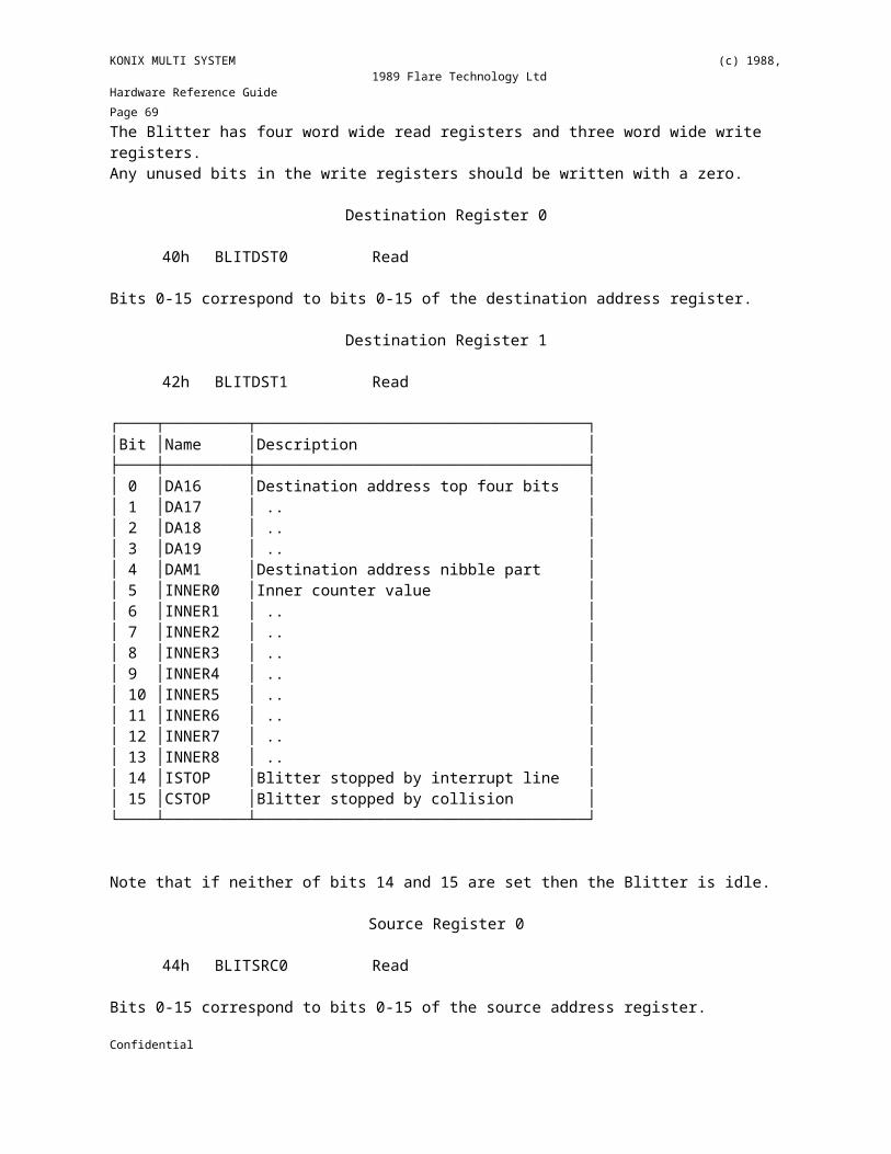
KONIX MULTI SYSTEM (c) 1988, 1989 Flare Technology LtdHardware Reference Guide Page 69
Constants
The ROM constants and data-space registers in the machine have a set of pre-defined names built in to the assembler, to save the user having to type them in every time. These are defined as if the SET directive had been used, allowing them to be re-defined if desired. They are:
┌─────────┬─────────┬────────────────┐ │Address │Data │Name │ ├─────────┼─────────┼────────────────┤ │000 │ │SINE │ │100 │0000 │H0000 or ZERO │ │101 │0001 │H0001 or ONE │ │102 │0002 │H0002 or TWO │ │103 │0004 │H0004 or FOUR │ │104 │0008 │H0008 or EIGHT │ │105 │0010 │H0010 or SIXTEEN│ │106 │0020 │H0020 │ │107 │0040 │H0040 │ │108 │0080 │H0080 │ │109 │FFFF │HFFFF or MINUS1 │ │10A │FFFE │HFFFE or MINUS2 │ │10B │FFFC │HFFFC or MINUS4 │ │10C │8000 │H8000 │ │140 │ │R_INTRA │ │141 │ │R_INDEX │ │142 │ │R_DMA0 │ │143 │ │R_DMA1 │ │144 │ │R_DMD │ │145 │ │R_MZ0 │ │146 │ │R_MZ1 │ │147 │ │R_Z2 │ │148 │ │R_DAC1 │ │149 │ │R_DAC2 │ │14A │ │R_PC │ │14B │ │R_MODE │ │14C │ │R_X │ │14D │ │R_AZ │ │14E │ │R_INTRD │ │14F │ │R_DSPIO │ └─────────┴─────────┴────────────────┘
Error Reporting
Confidential

KONIX MULTI SYSTEM (c) 1988, 1989 Flare Technology LtdHardware Reference Guide Page 70 Error messages are printed during pass 2. If a listing is being produced the messages will be written into the file as well as displayed on the screen. Only one error message per line is written to the file but a number of error messages per line may be displayed on the display. The messages shown on the display will provide more detailed information about the error.
Messages have a standard format.
(1) (2) (3) (4) (5) (6)*** SOURCE.S(nn) : macro ADD2 line nn Syntax error*** SOURCE.S(nn) : Syntax error
(1)The error message tag.(2)The name of the source file currently being worked on, this will
be the name of an include file if appropriate.
(3)The line number of the source file that the error occurred on.(4)If the source line has invoked a macro the name is given.(5)Ditto, the line number in the macro that contains the error.(6)The error description.
The messages are presented in this way so that an error may be quickly located. Even if macros invoke macros the name of the macro that contains the error is reported. This is especially useful when the bodies of the macros are not listed through the use of listing control directives.The messages are also output to the console in the format above, omitting the asterisk prefix. As this format is broadly compatible with >>Microsoft MASM>>, intelligent editors such as >>Brief>> will be able to parse them and display them to the user within the editor.
Confidential