gal
TRANSCRIPT

1 FPGA IMPLEMENTATION OF DSSS-CDMA TRANSMITTER AND RECEIVER FOR ADHOC NETWORKS 1 B.Sreedevi, M.Tech 2 V.Vijaya, (PhD) M.Tech 3 Ch.Kranthi Rekh, Assoc. Professor. VCEW Assoc. Professor. VCEW, Asst.Professor LUC, Mantin, Malaysia [email protected] [email protected] [email protected] 4 Rama Valupadasu (Ph D), M.Tech 5 B.RamaRao Chunduri, PhD., M.Tech Asst.Professor NIT, Warangal Professor NIT, Warangal [email protected] [email protected]
Abstract— The DS - CDMA is expected to be the major medium access technology in the future mobile systems owing to its potential capacity enhancement and the robustness against noise. The CDMA is uniquely featured by its spectrum-spreading randomization process employing a pseudo-noise (PN) sequence, thus is often called the spread spectrum multiple access (SSMA). As different CDMA users take different PN sequences, each CDMA receiver can discriminate and detect its own signal, by regarding the signals transmitted by other users as noise- like interferences. In this project Direct sequence principle based CDMA transmitter and receiver is implemented in VHDL for FPGA. The digital frequency synthesizer principle is used in generating the carrier signals both at transmitter and receiver modules. The transmitter module mainly consists of symbol generator, programmable PN sequence generator, digital local oscillator, spreader and BPSK modulator blocks. The receiver module consists of BPSK demodulator, matched filter, programmable PN sequence generator and threshold detector blocks. The CDMA receiver gets this input and recovers the data using matched filter.Modlesim Xilinx Edition 5.8 (MXE) tool will be used for functional simulation and logic verification at each block level and system level. The Xilinx Synthesis Technology (XST) of Xilinx ISE tool will be used for synthesis of transmitter and receiver on FPGAs. Applications of the developed CDMA system for ADHOC networks and defense communication links will be studied. The possible extensions of work in view of advancements in software defined radio principles will be discussed. Keywords—DDFS, DS-CDMA, LFSR, PN code, spread spectrum.
INTRODUCTION Cellular technology has grown tremendously both in terms of traffic and the services it offers [1-2]. The mobile telecommunication industry facing the problem providing technology that be able to support a variety of services ranging from voice communication with a bit rate of few Kbps to wireless multimedia in which bit rate up to 2 Mbps. This tremendous growth has also been fueled by the recent improvements in the capacity of wireless links due to the use of multiple access techniques. The idea is to transmit signals simultaneously through a linear band limited channel without inter channel or inter symbol interference [5].
To design multi channel transmission must concentrate on reducing cross talk between adjacent channels. One of the most promising cellular standards is IS-95A code
division multiple access (CDMA) system[2]. The advantages of IS-95A CDMA standard over other standards are optimum subscriber station power management, bandwidth recycling, efficient power control, multilayer diversity and compatability. The forward link frequency is in the range of (869-894) MHz and reverse link frequency is in the range of (824- 849) MHz. In the mobile communication transmission from the base station to mobile receiver are on the forward link and the transmission from the mobile user to the base station are on the reverse link[4].
VHDL implementation of DS-CDMA transmitter and receiver has been proposed in this thesis. In this project pseudo noise code is generated by using two six bit LFSRs.Code signal is called as chip signal. The chips modulated by the carrier using a digital modulation technique BPSK. The carrier is generated by using the technique discrete digital frequency synthesizer. CDMA base stations must be able to discriminate this different code sequences in order to distinguish one transmission from other .This discrimination is accomplished by means of a matched code filter .A matched code filter is a filter whose frequency spectrum is exactly designed to match the frequency spectrum of the input signal. Here matched code filter generating the pseudo noise code, generated noise code is correlated with the received code and detecting original data.
In the recent years the CDMA on FPGA platform has attracted attention of academic research and industry. The Spartan TM-3E family of Field-Programmable Gate Arrays (FPGAs) is specifically broadband designed to meet the needs of high volume, cost-sensitive consumer electronic applications. The five-member family offers densities ranging from 100,000 to 1.6 million system gates. Because of their exceptionally low cost, Spartan -3E FPGAs are ideally suited to a wide range of consumer electronics applications, including access, home networking, display/projection, and digital television equipment.
I. CODE DIVISION MULTIPLE ACCESS
Code Division Multiple Access (CDMA) is a spread spectrum technique that uses neither frequency channels nor time slots [3-5]. With CDMA, the narrow band message (typically digitized voice data) is multiplied by a large bandwidth signal that is a pseudo random noise code (PN code). All users in a CDMA system use the same frequency band and transmit simultaneously. The transmitted signal is recovered by correlating the received signal with the PN code
2011 IEEE Symposium on Computers & Informatics
978-1-61284-691-0/11/$26.00 ©2011 IEEE 255

used by the transmitter. Figure 1 shows the general use of the spectrum using CDMA.
Figure 1 Code division multiple access (CDMA)
CDMA technology was originally developed by the military during World War II. Researchers were spurred into looking at ways of communicating that would be secure and work in the presence of jamming. Some of the properties that have made CDMA useful are [3]: • Signal hiding and non-interference with
existing systems. • Anti-jam and interference rejection • Information security • Accurate Ranging • Multiple User Access • Multipath tolerance
A. CDMA Process Gain One of the most important concepts required in
order to understand spread spectrum techniques is the idea of process gain. The process gain of a system indicates the gain or signal to noise improvement exhibited by a spread spectrum system by the nature of the spreading and despreading process.
Where transmitted bandwidth after the
data is spread, and BWinfo is the bandwidth of the information data being sent.
The data to be transmitted (a) is spread before transmission by modulating the data using a PN code. This broadens the spectrum as shown in (b). In this example the process gain is 125 as the spread spectrum bandwidth is 125 times greater the data bandwidth. Part (c) shows the received signal.
2
Figure 2 Basic CDMA transmissions. B. CDMA Generation
CDMA is achieved by modulating the data signal by a pseudo random noise sequence (PN code), which has a chip rate higher then the bit rate of the data.. Figure 3 shows a basic CDMA transmitter [2-4].
Figure 3 Simple direct sequence modulator
The PN code used to spread the data can be of two main types. A short PN code (typically 10-128 chips in length) can be used to modulate each data bit. Figure 4 shows the generation of a CDMA signal using a 10-chip length short code. Alternatively a long PN code can be used
Figure 4 Direct sequence signals
C. CDMA Forward Link Encoding The forward link, from the base station to the
mobile, of a CDMA system can use special orthogonal PN codes, called Walsh codes, for separating the multiple users on the same channel. These are based on a Walsh matrix, which is a square matrix with binary elements and dimensions that are a power of two. It is generated from the basis that Walsh (1) = W1 = 0 and that: Where Wn is the Walsh matrix of dimension n. For example:
256
Walsh codes are orthogonal, which means that the dot product of any two rows is zero. This is due to the fact that for any two rows exactly half the number of bits match and half do not. Each row of a Walsh matrix can be used as the PN code of a user in a CDMA system.
D.CDMA Reverse Link Encoding The reverse link is different to the forward link
because the signals from each user do not originate from a same source as in the forward link. The transmission from each user will arrive at a different time, due to propagation delay, and synchronization errors. Due to the unavoidable timing errors between the users, there is little point in using Walsh codes as they will no longer be orthogonal. For this reason, simple pseudo random sequences are typically used. These sequences are chosen to have a low cross correlation to minimize interference between users. The capacity is different for the forward and the reverse links because of the differences in modulation. The reverse link is not orthogonal, resulting in significant inter-user interference. For this reason the reverse channel sets the capacity of the system [1-2].
II.TYPES OF CDMA TECHNIQUES Based on the modulation method the
CDMA technique can be classified into three categories. CDMA: direct sequence (DS) CDMA: frequency hopping (FH) CDMA: time hopping (TH)
A . CDMA Properties • Multiple access capability • Protection against multipath interference • Privacy, interference rejection • Anti-jamming capability • Low probability of interception
B. DIRECT Sequence The spreading of the signal is done by using the
pseudonoise sequence. Let's say that a binary information sequence with an information rate of R bits per second is to be spread. The bit interval of the signal is Tb = 1/R seconds and the available channel bandwidth is Bc Hz, where Bc >> R[4-5]
At the modulator the bandwidth of the information signal is expanded to W = Bc Hz by shifting the phase of the transmitted signal pseudorandomly at a rate of W times per second according to the pattern of the PN generator. The effective bit rate will therefore depend on the available bandwidth Bc, and the length of the PN-sequence N as
⎛ 1 ⎞
R = B ∗⎜ ⎟
b c ⎜⎝ (1 + N )
⎟⎠
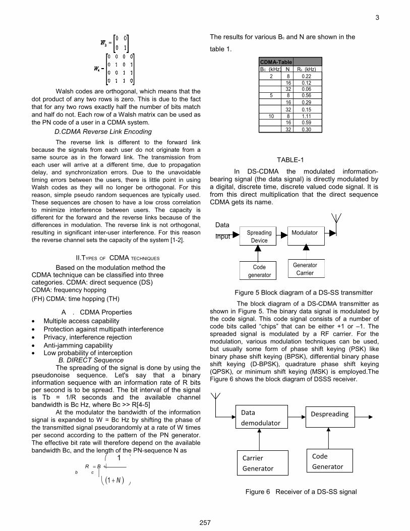
3 The results for various Bc and N are shown in the
table 1.
CDMA-Table BC (kHz) N Rb (kHz)
2 8 0.22 16 0.12 32 0.06
5 8 0.56 16 0.29 32 0.15
10 8 1.11 16 0.59 32 0.30
TABLE-1 In DS-CDMA the modulated information-
bearing signal (the data signal) is directly modulated by a digital, discrete time, discrete valued code signal. It is from this direct multiplication that the direct sequence CDMA gets its name.
Data
Input Spreading Modulator
Device
Code Generator
Carrier
generator
Figure 5 Block diagram of a DS-SS transmitter The block diagram of a DS-CDMA transmitter as
shown in Figure 5. The binary data signal is modulated by the code signal. This code signal consists of a number of code bits called “chips” that can be either +1 or –1. The spreaded signal is modulated by a RF carrier. For the modulation, various modulation techniques can be used, but usually some form of phase shift keying (PSK) like binary phase shift keying (BPSK), differential binary phase shift keying (D-BPSK), quadrature phase shift keying (QPSK), or minimum shift keying (MSK) is employed.The Figure 6 shows the block diagram of DSSS receiver.
Figure 6 Receiver of a DS-SS signal
Data demodulator
Despreading
Carrier Generator
Code Generator
257
After transmission of the signal, the receiver shown in Figure 6 dispreads the SS signal using a locally generated code sequence.
A PN code is a sequence of chips valued -1 and 1 (polar) or 0 and 1 (non-polar) and has noise-like properties. This results in low cross- correlation values among the codes and the difficulty to jam or detect a data message. A usual way to create a PN code is by means of at least one shift-register. When the length of such a shift-register is n, the following can be said about the period NDS of the above mentioned code-families:
NDS = 2n -1.
Indirect- sequence systems the length of the code is the same as the spreading-factor with the consequence that:
Gp(DS) = NDS.
Figure 7 Direct-sequence spreading
4
and B is low, the correlation between the received signal from the interfering transmitter and code A can be higher than the correlation between the received signal from the intended transmitter and code A. The result is that proper data detection is not possible [5].
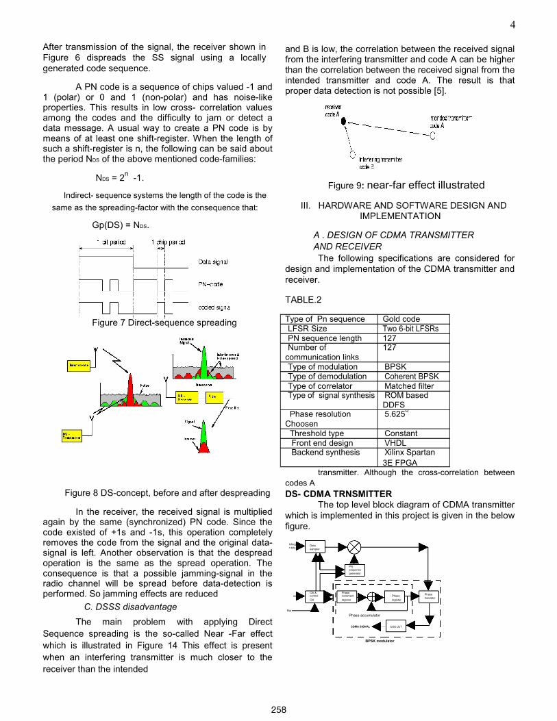
Figure 9: near-far effect illustrated
III. HARDWARE AND SOFTWARE DESIGN AND
IMPLEMENTATION
A . DESIGN OF CDMA TRANSMITTER AND RECEIVER The following specifications are considered for
design and implementation of the CDMA transmitter and receiver. TABLE.2
Type of Pn sequence Gold code LFSR Size Two 6-bit LFSRs PN sequence length 127 Number of 127
communication links Type of modulation BPSK Type of demodulation Coherent BPSK Type of correlator Matched filter Type of signal synthesis ROM based
DDFS Phase resolution 5.6250
Choosen Threshold type Constant Front end design VHDL Backend synthesis Xilinx Spartan
3E FPGA
Figure 8 DS-concept, before and after despreading
In the receiver, the received signal is multiplied again by the same (synchronized) PN code. Since the code existed of +1s and -1s, this operation completely removes the code from the signal and the original data-signal is left. Another observation is that the despread operation is the same as the spread operation. The consequence is that a possible jamming-signal in the radio channel will be spread before data-detection is performed. So jamming effects are reduced
C. DSSS disadvantage The main problem with applying Direct
Sequence spreading is the so-called Near -Far effect which is illustrated in Figure 14 This effect is present when an interfering transmitter is much closer to the receiver than the intended
transmitter. Although the cross-correlation between codes A DS- CDMA TRNSMITTER
The top level block diagram of CDMA transmitter which is implemented in this project is given in the below figure.
Informatio Data
n bits
sampler
PN
sequence
generator
Clk & Phase
Phase Phase
control increment
translator
Ckt register register
Rst
Phase accumulator
CDMA SIGNAL COS LUT
BPSK modulator
258
Figure 10 Block diagram of CDMA transmitter.
B . DS-CDMA RECEIVER The DS-CDMA receiver implemented in this project
with the specification mentioned in the above sections consists of following blocks.
The high level block diagram of CDMA receiver is shown in the Figure 11.
Figure 11: Block diagram of CDMA Rx
C . VHDL IMPLEMENTATION OF CDMA TRANSMITTER AND RECEIVER
A VHDL specification can be executed in order to achieve high level of confidence in its correctness before commencing design and may simulate one to two orders of magnitude faster than a gate level description
IV. RESULT ANALYSIS: PN Sequence generator:
5 BPSK Modulator
Figure 14 Simulation results for BPSK modulator Figure 15: Simulation results for Single user CDMA Tx & Rx
Figure
The gold code generator is tested with input t11, t12, t21; t22, key and output observed are pn_seq1, pn_seq2. Direct Digital Frequency Synthesizer
Direct Digital Frequency Synthesizer is a technique to produce desired out put with full digital control. Figure 13 Simulation results for DDFS
Frequency of the carrier generated is fc= fclk/64 = fck/26
Figure 16: Simulation results for four user Tx & Rx
V. CONCLUSIONS CDMA is one of the most impartant multiple access technique .In this project the transmitter and receiver were implemented on FPGA. After synthesis simulations are agreed before synthesis simmulations. The transmitter was connected to the receiver before synthesis was done to verify functionality of the transmitter and receiver. This has been tested using an arbitrary chosen data stream, where these data have been transmitted through implemented transmitter and then received by our implemented receiver. A comparison has been done betweenn the transmitted and received data and satisfactory results have been achieved. Increasing the number of bits using the same topology, it is possible to reach the standard rates specified for CDMA.
This work has the following applications. Custom CDMA communication setup with specified
PN sequence length and number of users Standard CDMA systems designs such as used
for mobiles and GPS
259

Implementation of a CDMA communication system with DSSS technique in VHDL has the following advantages
The design is fully reconfigurable The number of bits and PN sequence can be
changed very easily Useful for both FPGA and ASIC
implementations. Disadvantages Complex hardware is involved in receiver design
which increases the cost of the system. FUTURE SCOPE
The concept can be extended to design the GPS system which is CDMA system with 1023 chip length technique.
ACKNOWLEDGMENT
We are grateful to management Vaagdevi college of Engineering, Warangal for the facilities to provide to complete the project in time.
REFERENCES [1] William C.Y.Lee, Mobile Cellular Telecommunications
Systems, McGraw-Hill International Edditions , 1997. [2] John G. Proakis and Masoud Salehi. “Communications
Systems Engineering” Prentice Hall, Inc. Englewood Cliffs,
New Jersey 1994.
[3] Rodger E. Ziemer and Roger L. Peterson. “Digital
Communications and SpreadSpectrum Systems” Macmillian
Publishing Company, New York 1985.
[4] S. Allevad, T. Andersen m,m. ”Acoustic
Communication System With Two Branch Diversity”,
Communication Project, Stockholm 2000. [5] M.K. Simon, D.Divsalar and D.Raphaehi “improved
parallel intereferencecancellation for CDMA” IEEE Trans.
Commun..vol. 46 Feb 1998.
[6] “IS-95A CDMA,” Technical report from Yonsei University, 2002
Bibliographical notes: B.Sreedevi obtained her AMIE Degree in Electronics & Communication Engg., from Institution of Engineers, Calcutta, and M.Tech. Degree in Digital System Computer Electronics, from JNTUA college of Engg Ananthapur. She is working as Associate Professor in the ECE Dept of Vaagdevi College of Engineering at Warangal. She has 10 years of Teaching Experience. Attended 12 workshops/refresher courses/short term courses at various places. Member of Project Review Committee (UG/PG); CRC for (UG/PG). Her area of interest are Image processing, Signal processing, VLSI, Communications. She is the project coordinator for UG/PG.She is the course coordinator for PG course.She is life
member of ISTE, IETE. She has published no. of papers in national conferences and international conferences.
V.Vijaya obtained her B.Tech Degree in Electronics & Communication Engg., from (JNTU) Jawaharlal Nehru Technological University College of Engg., Ananthapur, and M.Tech. Degree in Instrumentation and Control Systems, from JNTUK college of Engg Kakinada and Pursuing PhD from JNTUH, Hyderabad. V.Vijaya worked at APEL Radio Communication Systems, Hyderabad and presently, she is working as Associate Professor in the ECE Dept of Vaagdevi College of Engineering at Warangal. She has 10 years of Teaching Experience and 2 years of Industrial Experience. Attended 15 workshops/refresher courses/short term courses at various places. Member of Project Review Committee (UG/PG); CRC for (UG/PG).She is the project coordinator for UG/PG. Her area of interest are Image processing, Signal processing, VLSI, Mobile Communications, Wireless Communications. She is life member of ISTE, IETE.She is the member of IEEE. She has published no.of papers in national conferences and international conferences.
V.Rama obtained her B.Tech in Electronics & Communication Engg., from JNTU, Kakinada, and M.Tech. from NIT, Warangal. Pursuing PhD from NIT, Warangal She is working as Asst Professor in the ECE Dept., at NIT, Warangal. Staff adviser of ECE Dept., Incharge for basic Electronics Lab. She involved in extracurricular activites at institute. She has 12 years of Teaching Experience. She organized no. of UGC workshops in NITW. Her area of research is Bio Medical Signal Processing. Her areas of interest are Image processing, Signal processing, Tele medicine. She has published no. of papers in national and international conferences.
CH.Kranthi Rekha had received her B.E in Electronics and Communication Engineering from Madurai Kamaraj University in 2000 and Completed M.Tech from JNTUH, Hyderabad. Presently she is working as Lecturer in Linton university college, Mantin, Malaysia, She has more than 10 years of teaching experience. She is the Author of two Books (Digital communications and Digital Image processing). Organized student level technical symposium technocraft-’09. Attended 10 workshops/refresher courses/short term courses at various places. As a resource person to talk on Image processing. Member of Project Review Committee (UG/PG); CRC for (UG/PG). Her area of interest are Neural networks, Image processing, Signal processing, VLSI, Communications. She is life member of ISTE, IETE. She has published no. of papers in national conferences and international conferences.
C.B.RamaRao obtained his B.Tech in Electronics & Communication Engg., from JNTU, Kakinada, and M.Tech. from jNTU, Kagpur PhD from IIT, karagpur.He is working as Professor in the ECE Dept., at NIT, Warangal. Head of the ECE Dept.,. He involved in extracurricular activites at institute. He has 25 years of Teaching Experience. He organized no. of UGC workshops in NITW. His area of research is Bio Medicalsignalprocessing.
260