1 application specific integrated circuits. 2 what is an asic? an application-specific integrated...
Post on 21-Dec-2015
225 views
TRANSCRIPT
1
Application Specific Integrated Circuits

2
What is an ASICWhat is an ASIC??
An application-specific integrated circuit (ASIC) is an
integrated circuit (IC) customized for a particular use
3
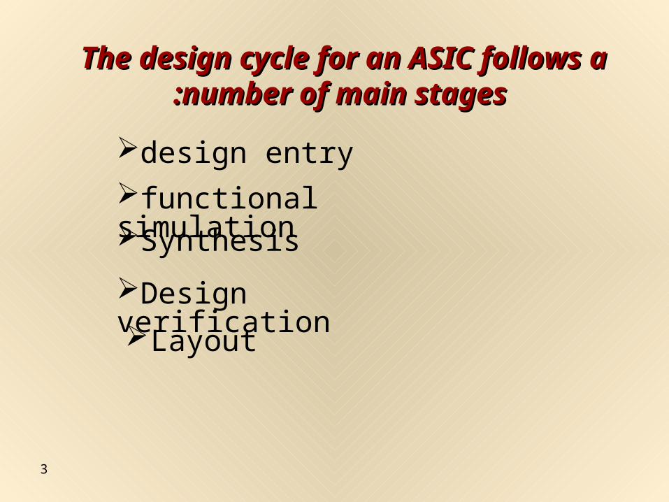
Layout
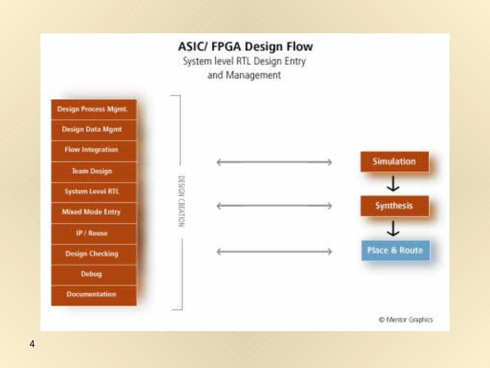
The design cycle for an ASIC follows aThe design cycle for an ASIC follows a number of main stagesnumber of main stages::
design entryfunctional simulationSynthesis
Design verification
4
5
Design DescriptionDesign Description
At initial stage of design process designer
provides a Behavioral description of the
functionality intended.
Behavioral model does not care about the
structure of the design, and does not include
timing information.
6
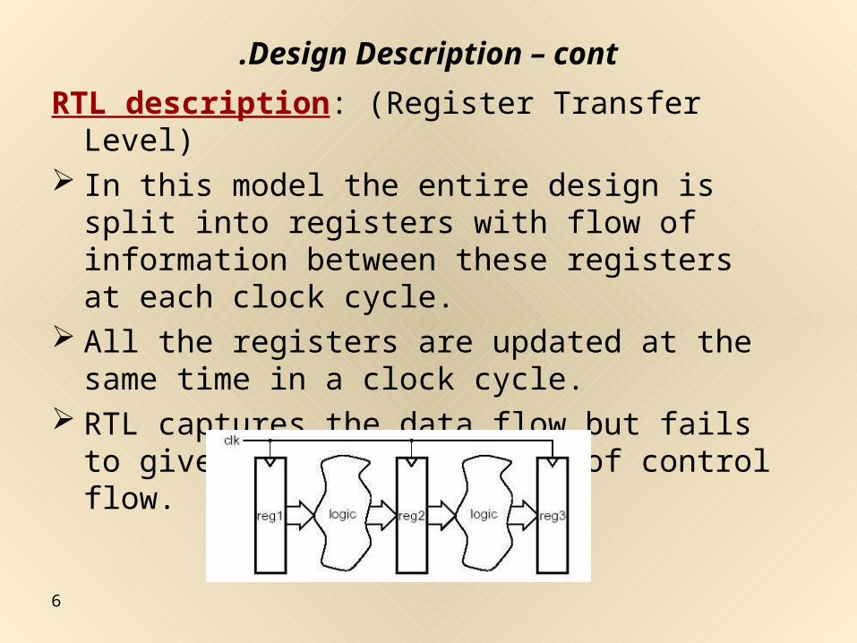
Design Description – cont.
RTL description: (Register Transfer Level) In this model the entire design is split into
registers with flow of information between these registers at each clock cycle.
All the registers are updated at the same time in a clock cycle.
RTL captures the data flow but fails to give a good description of control flow.
7
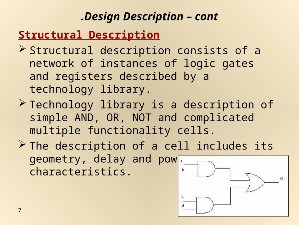
Design Description – cont.
Structural Description Structural description consists of a network of
instances of logic gates and registers described by a technology library.
Technology library is a description of simple AND, OR, NOT and complicated multiple functionality cells.
The description of a cell includes its geometry, delay and power characteristics.
8
functional simulationfunctional simulation
There are mainly three classes of logic
simulators:
1. compiled code logic simulators.
2. event-driven logic simulators.
9
functional simulation – cont.
Compiled code logic simulator:
Compiled code logic simulation algorithmevaluates every logic element in the design ateach time step. In a compiled code simulator a combinational
circuit is topologically ordered and equation is generated for each gate output in terms of its inputs using Boolean operators AND, OR and NOT.
since circuit activity is very low at each element, run time of such algorithm is huge for big circuits.
10
Interpretive Event Driven logic simulator: Event-driven logic simulator works on the principle
that output of a logic element changes only when one of its inputs change.
Statistical data shows that event activities in large circuits are very low and with increase in size of the circuit percentage activity on a logic element decreases.
one major class of event driven logic simulation algorithms is Asynchronous Simulation Algorithms.
functional simulation – cont.
11
functional simulation – cont.
This algorithm has two different conservative
and optimistic approaches:
1. In conservative schemes only safe evaluation time is allowed, evaluations which guarantee correct result. A logic element is evaluated only after it receives all its input tokens. As a logic element is evaluated its output is decided on the basis of its inputs and time stamp of output is decided by time stamp of last arriving token and delay of the logic element.
12
functional simulation – cont.
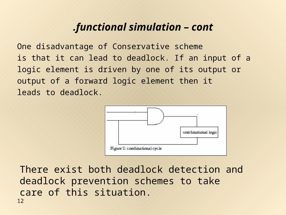
One disadvantage of Conservative scheme
is that it can lead to deadlock. If an input of a
logic element is driven by one of its output or
output of a forward logic element then it
leads to deadlock.
There exist both deadlock detection and deadlock prevention schemes to take care of this situation.
13
functional simulation – cont.
2. In optimistic scheme evaluation of a logic element takes place as soon as an input token arrives at its input. If the output produced turns out to be incorrect then roll back takes place to return to previous know correct state and messages are sent to forward elements to cancel effect of incorrect message sent earlier. This algorithm does not lead to deadlocks but has an added cost of state saving and more complex control mechanism because of rollback. Optimistic scheme is most efficient as long as rollbacks are few.
14
ASIC SynthesisASIC Synthesis
RTL Synthesis involves three major steps:
1. Transition from RTL description into gates and flip-flops. (in order to reduce number of gates in the design)
2. Optimization of logic.
3. Placement and routing of optimized netlist.
15
ASIC Synthesis – cont.
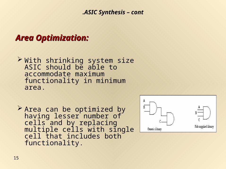
With shrinking system size ASIC should be able to accommodate maximum functionality in minimum area.
Area can be optimized by having lesser number of cells and by replacing multiple cells with single cell that includes both functionality.
Area Optimization:Area Optimization:
16
ASIC Synthesis – cont.
Development of hand-held devices has led to reduction of battery size and hence low power consuming systems.
Low power consumption has become a big
requirement for lot of designers.
Timing OptimizationTiming Optimization
Designer specifies maximum delay between primary input and primary output.
Power OptimizationPower Optimization
17
ASIC Synthesis – cont.
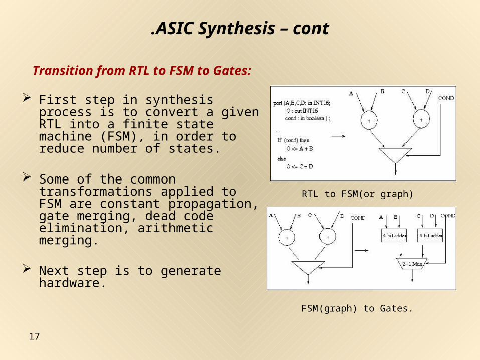
Transition from RTL to FSM to Gates:
First step in synthesis process is to convert a given RTL into a finite state machine (FSM), in order to reduce number of states.
Some of the common transformations applied to FSM are constant propagation, gate merging, dead code elimination, arithmetic merging.
Next step is to generate hardware.
RTL to FSM(or graph)
FSM(graph) to Gates.

18
ASIC Synthesis – cont.
Gate Level Logic Optimization Timing and area constraints are provided by the
designer. Slack is defined as difference between the
expected arrival time and actual arrival time of signal at a particular output port.
Slack is calculated for input to output paths. The aim of timing optimization is to reduce the
slack.
19
ASIC Synthesis – cont.
3) converting all Boolean logic to 2 level sum-of-products
produces very fast designs but increases area.
For example (a + b) ( c + d) = ac + bc + ad + bd
Optimizations to reduce area include following:
1) Constant propagation: Boolean minimization may lead to dissolution of certain section of code into constants. Such constants should be propagated at this stage in order to reduce gate count and area.
2) Eliminate redundant logic: For example a + ab should be replaced by a.0
20
ASIC Synthesis – cont.
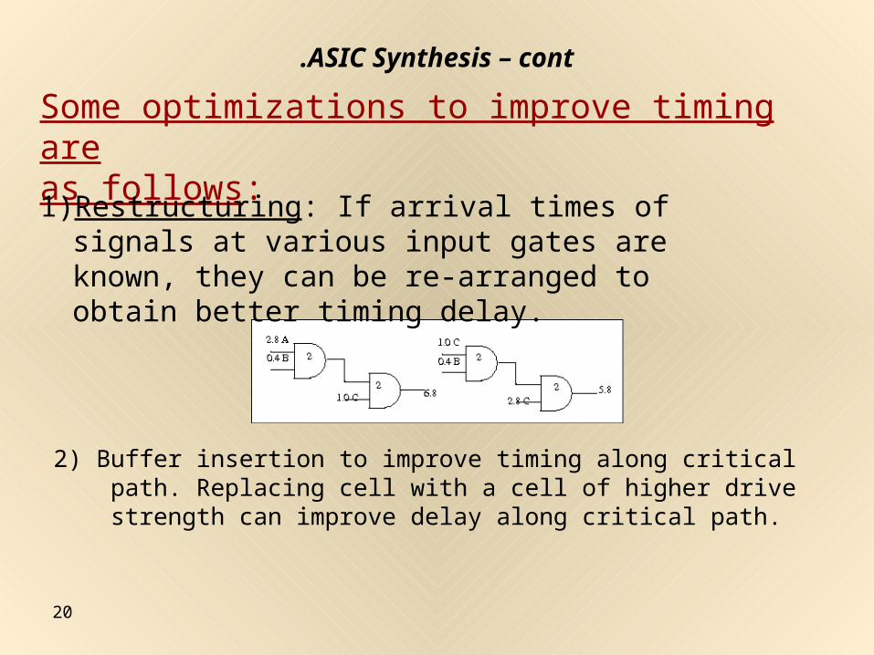
2) Buffer insertion to improve timing along critical path. Replacing cell with a cell of higher drive strength can improve delay along critical path.
Some optimizations to improve timing areas follows:
1) Restructuring: If arrival times of signals at various input gates are known, they can be re-arranged to obtain better timing delay.

21
ASIC Synthesis – cont.
3. Pin assignment can be changed to match the late arriving input pin with pin having faster propagation delay to output.
22
ASIC Synthesis – cont.
Area ReclamationCertain timing optimizations might lead to area
escalation. Area Reclamation algorithms try to reclaim
area which does not affect timing on critical paths.
Downsizing the gates which contain extra pins.
Buffers which were inserted to reach fan-out constraint and are unnecessary are removed.
23
VerificationVerification
Biggest challenge in IC design is verification because the cost of single error is huge.
One type of verification methods include Simulation, and Emulation and hardwareacceleration.
Emulator is a hardware device that can be used to emulate a piece of hardware functionality. It is commonly used as a debugging tool to test a system under development for functional correctness.
24
- cont.Verification
Emulation is a faster solution to verification
problem. In Emulation a portion of emultable
design is synthesized and optimized.
Emulators are able to provide execution
speed close to real time. This allows
verification engineers to reduce Verification
time.
25
Gate-level simulation and Gate-level simulation and ExtractionExtraction
Placement and routing involves placement of modules on chip area and routing interconnect between various modules.
26
Gate-level simulation and Extraction – cont.
Various aspects of signal integrity include:
1. Technology scale down:
Aluminium has been used until recently to
manufacture interconnects but increasing
contribution of interconnects in signal
propagation has forced IC manufacturers to
replace it with material like copper with lower
resistance.
27
Gate-level simulation and Extraction – cont.
2. CrossTalk: When two wire segments are closer to each other more than a minimum threshold, they will interfere in each other's functioning. Signal on one wire may weaken due to electromagnetic effects of signal carried by other wire. With diminishing technology size Crosstalk is major contributor to high speed IC defects.

28