1 chapter 5 defects. 2 5.1 introduction the defects in semiconductors include: (1)foreign...
Post on 20-Dec-2015
224 views
TRANSCRIPT

1
CHAPTER 5
DEFECTS

2
5.1 Introduction
The defects in semiconductors include:
(1)foreign interstitial (oxygen in silicon)
(2)foreign substitutional (dopant),
(3)vacancy,
(4)self interstitial,
(5)stacking fault,
(6)edge dislocation,
(7)precipitate.

3
Schematic representation of defects in semiconductors. The defect types are described in the text.
4
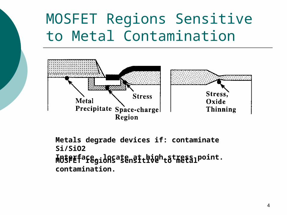
MOSFET regions sensitive to metal contamination.
MOSFET Regions Sensitive to Metal Contamination
Metals degrade devices if: contaminate Si/SiO2Interface, locate at high stress point.
5
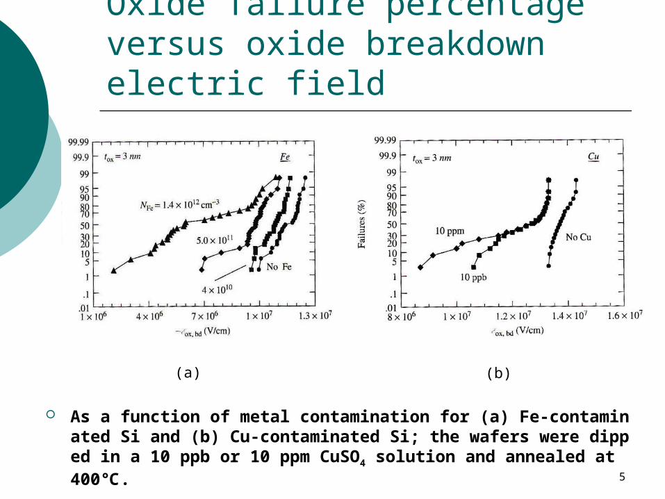
As a function of metal contamination for (a) Fe-contaminated Si and (b) Cu-contaminated Si; the wafers were dipped in a 10 ppb or 10 ppm CuSO4 solution and annealed at 400 . ℃
(a) (b)
Oxide failure percentage versus oxide breakdown electric field

6
5.2 GENERATION-RECOMBINATION STATISTICS
7
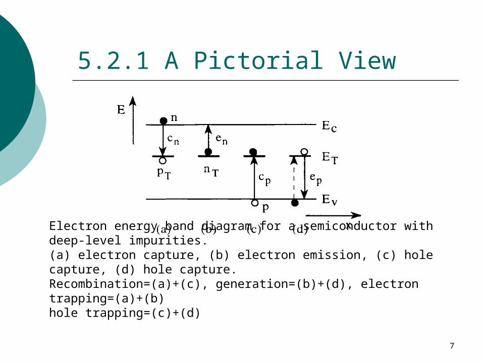
Electron energy band diagram for a semiconductor with deep-level impurities. (a) electron capture, (b) electron emission, (c) hole capture, (d) hole capture.Recombination=(a)+(c), generation=(b)+(d), electron trapping=(a)+(b)hole trapping=(c)+(d)
5.2.1 A Pictorial View

8
Whether an impurity acts as a trap or G-R
center depends on:
1. ET
2. the Fermi-level location in the bandgap
3. the temperature
4. the capture cross section of the impurity

9
5.2.2 A Mathematical Description
The time rate of change of n due to G-R mechanisms is given by (nT+pT=NT)
For holes, we find the parallel expression
The capture coefficient Cn is defined by
If the G-R center is a donor, nT is neutral and pT is positively charged.
If the G-R center is an acceptor, pT is neutral and nT is negatively charged.
(5.1)
(5.2)
(5.3)

10
When electrons and holes are recombined or are
generated, n, p, nT, pT are all functions of time.
cnn is the density of electrons captured per second.
en has a unit of 1/s, cn has a unit of cm-3/s.

11
Whenever an electron or hole is captured or emitted, the center occupancy change rate is (a)+(d)-(b)-(c)= ((d)-(c))-((a)-(b))
In the Quasi-neutral regions n and p are reasonably constant
The Steady-state density as t ∞ is
(5.4)
(5.5)
(5.6)

12
For an n-type substrate p can be neglected, Eq.(5.5) becomes
where τ1=1/(en+cnn+ep)
(5.7)

13
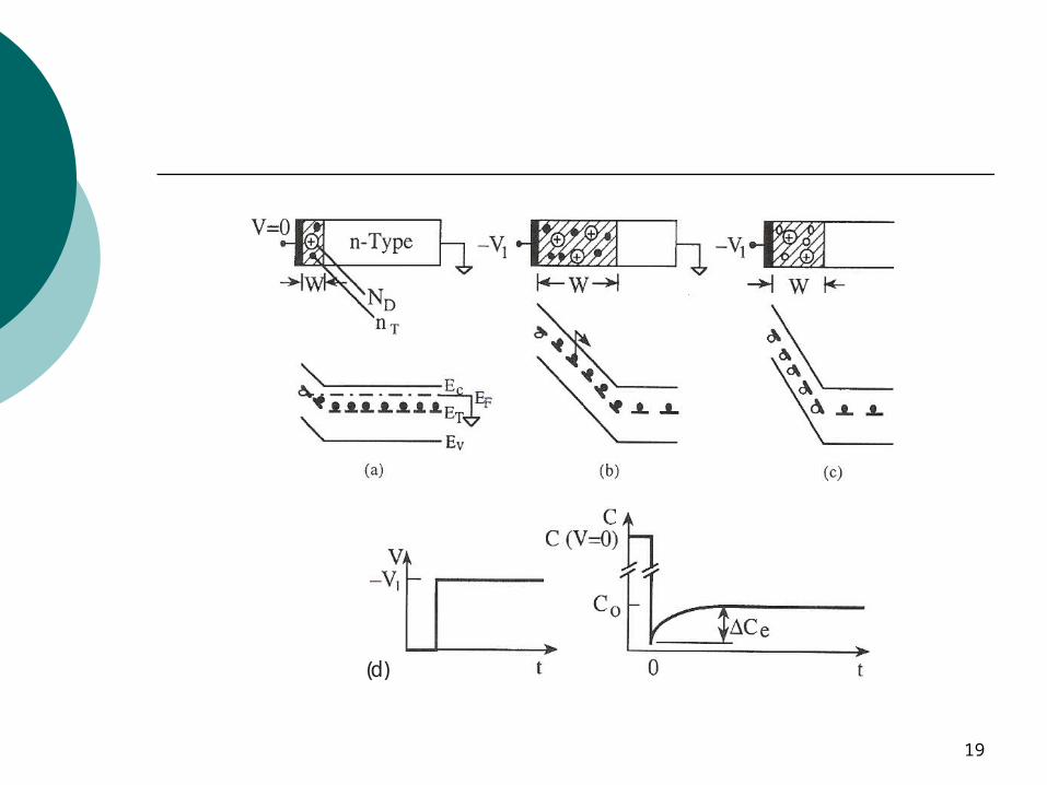
A Schottky diode for (a) zero bias, (b) reverse bias at t=0, (c) reverse bias as t→∞.
The applied voltage and resultant capacitance transient are show in (d)
Schottky Diode
(d)

14
During the initial emission period, the time dependence of nT simplifies to ( for traps in n-Si en>>ep, and in the depletion region n~0, )
(5.8)
(5.9)
The steady state trap density nT in the reverse-biased scr is
When bias is switched from reverse to zero, the time dependence of nT during the capture period is
(5.10)
ne e/1
nc/1 nC

15
5.3 CAPACITANCE MEASUREMENTS

16
Capacitance Measurements
The capacitance of the Schottky diode is
Nscr=ND+-nT
- for acceptor g-r center occupied by e- Nscr=ND
+ for acceptor g-r center occupied by h+
Nscr=ND+ for donor g-r center occupied by e- Nsc
r=ND++pT
+ for donor g-r center occupied by h+
(5.11)

17
5.3.1 Steady-State Measurements
For shallow-level donors and deep-level acceptors l /C2 is given as
If we define a slope S(t) = -dV / d(1/C2), then
(5.12)
(5.13)
For en>>ep, nT(0)~NT, nT(∞)~0.

18
5.3.2 Transient Measurements
1. Emission-Majority carriers
The capacitance increases with time for majority carrier emission, whether the substrate is p or n type and the impurities are donors or acceptors.
(5.14)
(5.15)
(5.16)
19
(d)

20
Plotting the capacitance difference
Under equilibrium conditions, dn/dt=0, hence
(5.17)
(5.18)
(5.19)
(5.20)
(5.21)

21
Assume the emission and capture coefficients remains equal to their equilibrium value under non-equilibrium conditions, then
With en=1/e and cn=vth, the emission time constant of electron and hole as
(5.22)
(5.23)
(5.24)
(5.25)

22
Electron energy diagram in equilibrium (1) and in the presence of an electric field(2) showing field-enhanced electron emission: (a) Poole-Frenkel emission, (b) phonon-assisted tunneling. The emission coefficient will be increased at high electrical field.

23
The electron thermal velocity is
(5.26)
(5.27)
(5.28)
24

25
τeT2 versus 1 / T plots for Si diodes containing Au and Rh.

26
(5.29)
τe can also be determined from plotting ln(S(∞)-S(t)) versus t.

27
For cp>>cn the acceptor g-r centers at t=0 nT 0 and N≒ scr N≒ D. When switched to zero bias holes are emitted and traps become negatively charged, then Nscr N≒ D-nT.The total negative charge in scr decreases and its width increases with time, the capacitance decreases with time.
2. Emission-Minority carriers
(5.30)
For P+n diode under forward bias, holes are injectedinto n-region, capture dominates emission, hence

28
The capacitance-time transients following majority carrier emission and minority carrier emission.

29
3. Capture – Majority Carrier
M-nSi is reverse biased for long enough time, traps are in the pT state. When the bias is off (0V), for a filling time tf
For tf<τc and the device is reverse biased again
(5.31)
(5.32)
(5.33)

30
(a) C - t response showing the capture and initial part of the emission process, (b) the emission C - t response as a function of capture pulse width.

31
(5.34)
(5.35)
4. Capture – Minority CarrierThe capture time during the filling time is:
The injected minority carrier density is varied by changing the forward bias.
(5.36)

32
5.4 CURRENT MEASUREMENTS
For transient current measurements, the integral of the I-t curve gives the total trapped charge. At high temperatures, I large and τ short; at low temperatures, I small and τ long. But the area under I-t curve is the same. Measure I-t at high temperatures and C-t at low temperatures give τ over ten orders of magnitude.

33
The measured current includes emission current Ie, displacement Id, and leakage current I1.
The emission current is
The displacement current is
(5.37)
(5.38)

34
The lower limit of the Ie integral (Eq. 5-37) should have been W(0V), for simplicity, it is set to 0. With dn/dt=ennT, and dnT/dt=-ennT
(5.39)

35
(5.40)
(5.41)

36
Drain current ID and gate capacitance CG transients of a 100μm × 150μm gate MESFET.

37
5.5 CHARGE MEASUREMENTS

38
Circuit for charge transient measurements.
Circuit for charge transient measurements.

39
Switch S is closed to discharge CF for t<0, at t=0 diode is reverse biased and S is open, such that the diode current charges the RFCF circuit and Vo changes with time.
For tF>>τe
(5.42)
(5.43)
(5.44)