1 kv rms quad-channel digital isolators data sheet ... · 1 kv rms quad-channel digital isolators...
TRANSCRIPT

1 kV RMS Quad-Channel Digital IsolatorsData Sheet ADuM7440/ADuM7441/ADuM7442
Rev. D Document Feedback Information furnished by Analog Devices is believed to be accurate and reliable. However, no responsibility is assumed by Analog Devices for its use, nor for any infringements of patents or other rights of third parties that may result from its use. Specifications subject to change without notice. No license is granted by implication or otherwise under any patent or patent rights of Analog Devices. Trademarks and registered trademarks are the property of their respective owners.
One Technology Way, P.O. Box 9106, Norwood, MA 02062-9106, U.S.A.Tel: 781.329.4700 ©2009–2015 Analog Devices, Inc. All rights reserved. Technical Support www.analog.com
FEATURES Small, 16-lead QSOP 1000 V rms isolation rating Safety and regulatory approvals
UL recognition UL 1577: 1000 V rms for 1 minute
Low power operation 5 V operation
2.25 mA per channel maximum at 0 Mbps to 1 Mbps 11.5 mA per channel maximum at 25 Mbps
3.3 V operation 1.5 mA per channel maximum at 0 Mbps to 1 Mbps 8.25 mA per channel maximum at 25 Mbps
Bidirectional communication Up to 25 Mbps data rate (NRZ) 3 V/5 V level translation High temperature operation: 105°C High common-mode transient immunity: >15 kV/μs
APPLICATIONS General-purpose, multichannel isolation SPI interface/data converter isolation RS-232/RS-422/RS-485 transceivers Industrial field bus isolation
GENERAL DESCRIPTION The ADuM7440/ADuM7441/ADuM74421 are 4-channel digital isolators based on the Analog Devices, Inc., iCoupler® technology. Combining high speed CMOS and monolithic air core transformer technologies, these isolation components provide outstanding performance characteristics superior to the alternatives, such as optocoupler devices and other integrated couplers.
The ADuM7440/ADuM7441/ADuM7442 family of quad 1 kV digital isolation devices is packaged in a small 16-lead QSOP. While most 4-channel isolators come in 16-lead wide SOIC packages, the ADuM7440/ADuM7441/ADuM7442 free almost 70% of board space and yet can still withstand high isolation voltage and meet UL regulatory requirements. In addition to the space savings, the ADuM7440/ADuM7441/ADuM7442 offer a lower price than 2.5 kV or 5 kV isolators where only functional isolation is needed.
This family, like many Analog Devices isolators, offers very low power consumption, consuming one-tenth to one-sixth the power of comparable isolators at comparable data rates up to 25 Mbps. Despite the low power consumption, all models of the ADuM7440/ADuM7441/ADuM7442 provide low pulse width distortion (<5 ns for C grade). In addition, every model has an input glitch filter to protect against extraneous noise disturbances.
The ADuM7440/ADuM7441/ADuM7442 isolators provide four independent isolation channels in a variety of channel configurations and two data rates (see the Ordering Guide) up to 25 Mbps. All models operate with the supply voltage on either side ranging from 3.0 V to 5.5 V, providing compatibility with lower voltage systems as well as enabling voltage translation functionality across the isolation barrier. All products also have an output default high logic state in the absence of the input power. 1 Protected by U.S. Patents 5,952,849, 6,873,065 and 7,075,329. Other patents
pending.
FUNCTIONAL BLOCK DIAGRAMS
ENCODE DECODE
ENCODE DECODE
ENCODE DECODE
ENCODE DECODE
VDD1A
GND1
VIA
VIB
VIC
VID
VDD1B
GND1
VDD2A
GND2
VOA
VOB
VOC
VOD
VDD2B
GND2
1
2
3
4
5
6
7
8
16
15
14
13
12
11
10
9
ADuM7440
08
34
0-0
01
Figure 1. ADuM7440
DECODE ENCODE
ENCODE DECODE
ENCODE DECODE
ENCODE DECODE
VDD1A
GND1
VIA
VIB
VIC
VOD
VDD1B
GND1
VDD2A
GND2
VOA
VOB
VOC
VID
VDD2B
GND2
1
2
3
4
5
6
7
8
16
15
14
13
12
11
10
9
ADuM7441
08
34
0-0
02
Figure 2. ADuM7441
DECODE ENCODE
DECODE ENCODE
ENCODE DECODE
ENCODE DECODE
VDD1A
GND1
VIA
VIB
VOC
VOD
VDD1B
GND1
VDD2A
GND2
VOA
VOB
VIC
VID
VDD2B
GND2
1
2
3
4
5
6
7
8
16
15
14
13
12
11
10
9
ADuM7442
08
34
0-0
03
Figure 3. ADuM7442

ADuM7440/ADuM7441/ADuM7442 Data Sheet
Rev. D | Page 2 of 20
TABLE OF CONTENTS Features .............................................................................................. 1 Applications ....................................................................................... 1 General Description ......................................................................... 1 Functional Block Diagrams ............................................................. 1 Revision History ............................................................................... 2 Specifications ..................................................................................... 3
Electrical Characteristics—5 V Operation................................ 3 Electrical Characteristics—3.3 V Operation ............................ 4 Electrical Characteristics—Mixed 5 V/3.3 V Operation ........ 5 Electrical Characteristics—Mixed 3.3 V/5 V Operation ........ 6 Package Characteristics ............................................................... 7 Regulatory Information ............................................................... 7 Insulation and Safety-Related Specifications ............................ 7
Recommended Operating Conditions .......................................7 Absolute Maximum Ratings ............................................................8
ESD Caution...................................................................................8 Pin Configurations and Function Descriptions ............................9 Typical Performance Characteristics ........................................... 12 Applications Information .............................................................. 14
PC Board Layout ........................................................................ 14 Propagation Delay-Related Parameters ................................... 14 DC Correctness and Magnetic Field Immunity ........................... 14 Power Consumption .................................................................. 15 Insulation Lifetime ..................................................................... 15
Outline Dimensions ....................................................................... 17 Ordering Guide .......................................................................... 17
REVISION HISTORY 10/15—Rev. C to Rev. D Change to Features Section and General Description Section ........ 1 Changes to Table 14 .......................................................................... 7 Updated Outline Dimensions ....................................................... 17 2/12—Rev. B to Rev. C Created Hyperlink for Safety and Regulatory Approvals Entry in Features Section ................................................................. 1 Change to PC Board Layout Section ............................................ 14 2/11—Rev. A to Rev. B Changes to Figure 7 ........................................................................ 11
8/10—Rev. 0 to Rev. A Change to Features ............................................................................ 1 Changes to Table 1 ............................................................................. 3 Added Note 1, Table 1 ....................................................................... 3 Changes to Table 4 ............................................................................. 4 Added Note 1, Table 4 ....................................................................... 4 Changes to Table 7 ............................................................................. 5 Added Note 1, Table 7 ....................................................................... 5 Changes to Table 10 .......................................................................... 6 Added Note 1, Table 10 ..................................................................... 6 Changes to Table 14 .......................................................................... 7 10/09—Revision 0: Initial Version
Data Sheet ADuM7440/ADuM7441/ADuM7442
Rev. D | Page 3 of 20
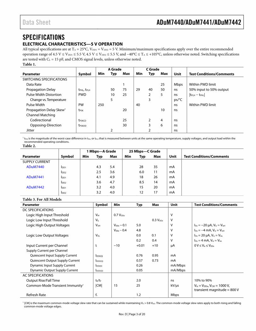
SPECIFICATIONS ELECTRICAL CHARACTERISTICS—5 V OPERATION All typical specifications are at TA = 25°C, VDD1 = VDD2 = 5 V. Minimum/maximum specifications apply over the entire recommended operation range of 4.5 V ≤ VDD1 ≤ 5.5 V, 4.5 V ≤ VDD2 ≤ 5.5 V, and −40°C ≤ TA ≤ +105°C, unless otherwise noted. Switching specifications are tested with CL = 15 pF, and CMOS signal levels, unless otherwise noted. Table 1. A Grade C Grade Parameter Symbol Min Typ Max Min Typ Max Unit Test Conditions/Comments SWITCHING SPECIFICATIONS
Data Rate 1 25 Mbps Within PWD limit Propagation Delay tPHL, tPLH 50 75 29 40 50 ns 50% input to 50% output Pulse Width Distortion PWD 10 25 2 5 ns |tPLH − tPHL|
Change vs. Temperature 5 3 ps/°C Pulse Width PW 250 40 ns Within PWD limit Propagation Delay Skew1 tPSK 20 10 ns Channel Matching
Codirectional tPSKCD 25 2 4 ns Opposing-Direction tPSKOD 30 3 6 ns
Jitter 2 2 ns 1 tPSK is the magnitude of the worst-case difference in tPHL or tPLH that is measured between units at the same operating temperature, supply voltages, and output load within the
recommended operating conditions. Table 2. 1 Mbps—A Grade 25 Mbps—C Grade Parameter Symbol Min Typ Max Min Typ Max Unit Test Conditions/Comments SUPPLY CURRENT
ADuM7440 IDD1 4.3 5.4 28 35 mA IDD2 2.5 3.6 6.0 11 mA ADuM7441 IDD1 4.1 4.9 18 26 mA IDD2 3.6 4.7 8.5 14 mA ADuM7442 IDD1 3.2 4.0 15 20 mA IDD2 3.2 4.0 12 17 mA
Table 3. For All Models Parameter Symbol Min Typ Max Unit Test Conditions/Comments
DC SPECIFICATIONS
Logic High Input Threshold VIH 0.7 VDDx V
Logic Low Input Threshold VIL 0.3 VDDx V
Logic High Output Voltages VOH VDDx − 0.1 5.0 V IOx = −20 µA, VIx = VIxH
VDDx − 0.4 4.8 V IOx = −4 mA, VIx = VIxH
Logic Low Output Voltages VOL 0.0 0.1 V IOx = 20 µA, VIx = VIxL
0.2 0.4 V IOx = 4 mA, VIx = VIxL
Input Current per Channel II −10 +0.01 +10 µA 0 V ≤ VIx ≤ VDDx Supply Current per Channel
Quiescent Input Supply Current IDDI(Q) 0.76 0.95 mA
Quiescent Output Supply Current IDDO(Q) 0.57 0.73 mA Dynamic Input Supply Current IDDI(D) 0.26 mA/Mbps Dynamic Output Supply Current IDDO(D) 0.05 mA/Mbps
AC SPECIFICATIONS
Output Rise/Fall Time tR/tF 2.0 ns 10% to 90%
Common-Mode Transient Immunity1 |CM| 15 25 kV/µs VIx = VDDx, VCM = 1000 V, transient magnitude = 800 V
Refresh Rate fr 1.2 Mbps 1 |CM| is the maximum common-mode voltage slew rate that can be sustained while maintaining VO > 0.8 VDD. The common-mode voltage slew rates apply to both rising and falling
common-mode voltage edges.

ADuM7440/ADuM7441/ADuM7442 Data Sheet
Rev. D | Page 4 of 20
ELECTRICAL CHARACTERISTICS—3.3 V OPERATION All typical specifications are at TA = 25°C, VDD1 = VDD2 = 3.3 V. Minimum/maximum specifications apply over the entire recommended operation range of 3.0 V ≤ VDD1 ≤ 3.6 V, 3.0 V ≤ VDD2 ≤ 3.6 V; and −40°C ≤ TA ≤ +105°C, unless otherwise noted. Switching specifications are tested with CL = 15 pF and CMOS signal levels, unless otherwise noted.
Table 4. A Grade C Grade Parameter Symbol Min Typ Max Min Typ Max Unit Test Conditions/Comments
SWITCHING SPECIFICATIONS Data Rate 1 25 Mbps Within PWD limit Propagation Delay tPHL, tPLH 60 85 37 51 66 ns 50% input to 50% output Pulse Width Distortion PWD 10 25 2 5 ns |tPLH − tPHL|
Change vs. Temperature 5 3 ps/°C Pulse Width PW 250 40 ns Within PWD limit Propagation Delay Skew1 tPSK 20 10 ns Channel Matching
Codirectional tPSKCD 25 3 5 ns Opposing-Direction tPSKOD 30 4 7 ns
Jitter 2 2 ns 1 tPSK is the magnitude of the worst-case difference in tPHL or tPLH that is measured between units at the same operating temperature, supply voltages, and output load
within the recommended operating conditions.
Table 5. 1 Mbps—A, C Grades 25 Mbps—C Grade Parameter Symbol Min Typ Max Min Typ Max Unit Test Conditions/Comments SUPPLY CURRENT
ADuM7440 IDD1 3.0 3.8 20 28 mA IDD2 1.8 2.3 4.0 5.0 mA ADuM7441 IDD1 2.8 3.5 14 20 mA IDD2 2.5 3.3 5.5 7.5 mA ADuM7442 IDD1 2.2 2.7 10 13 mA IDD2 2.2 2.8 8.4 11 mA
Table 6. For All Models Parameter Symbol Min Typ Max Unit Test Conditions/Comments DC SPECIFICATIONS
Logic High Input Threshold VIH 0.7 VDDx V Logic Low Input Threshold VIL 0.3 VDDx V Logic High Output Voltages VOH VDDx − 0.2 3.3 V IOx = −20 µA, VIx = VIxH VDDx − 0.4 3.1 V IOx = −4 mA, VIx = VIxH Logic Low Output Voltages VOL 0.0 0.1 V IOx = 20 µA, VIx = VIxL 0.2 0.4 V IOx = 4 mA, VIx = VIxL Input Current per Channel II −10 +0.01 +10 µA 0 V ≤ VIx ≤ VDDx Supply Current per Channel
Quiescent Input Supply Current IDDI(Q) 0.50 mA Quiescent Output Supply Current IDDO(Q) 0.41 mA Dynamic Input Supply Current IDDI(D) 0.18 mA/Mbps Dynamic Output Supply Current IDDO(D) 0.02 mA/Mbps
AC SPECIFICATIONS Output Rise/Fall Time tR/tF 2.8 ns 10% to 90% Common-Mode Transient Immunity1 |CM| 15 20 kV/µs VIx = VDDx, VCM = 1000 V,
transient magnitude = 800 V Refresh Rate fr 1.1 Mbps
1 |CM| is the maximum common-mode voltage slew rate that can be sustained while maintaining VO > 0.8 VDD. The common-mode voltage slew rates apply to both
rising and falling common-mode voltage edges.

Data Sheet ADuM7440/ADuM7441/ADuM7442
Rev. D | Page 5 of 20
ELECTRICAL CHARACTERISTICS—MIXED 5 V/3.3 V OPERATION All typical specifications are at TA = 25°C, VDD1 = 5 V, VDD2 = 3.3 V. Minimum/maximum specifications apply over the entire recommended operation range of 4.5 V ≤ VDD1 ≤ 5.5 V, 3.0 V ≤ VDD2 ≤ 3.6 V; and −40°C ≤ TA ≤ +105°C, unless otherwise noted. Switching specifications are tested with CL = 15 pF and CMOS signal levels, unless otherwise noted.
Table 7. A Grade C Grade Parameter Symbol Min Typ Max Min Typ Max Unit Test Conditions/Comments SWITCHING SPECIFICATIONS
Data Rate 1 25 Mbps Within PWD limit Propagation Delay tPHL, tPLH 55 80 30 42 55 ns 50% input to 50% output Pulse Width Distortion PWD 10 25 2 5 ns |tPLH − tPHL|
Change vs. Temperature 5 3 ps/°C Pulse Width PW 250 40 ns Within PWD limit Propagation Delay Skew1 tPSK 20 10 ns Channel Matching
Codirectional tPSKCD 25 2 5 ns Opposing-Direction tPSKOD 30 3 6 ns
Jitter 2 2 ns 1 tPSK is the magnitude of the worst-case difference in tPHL or tPLH that is measured between units at the same operating temperature, supply voltages, and output load
within the recommended operating conditions.
Table 8. 1 Mbps—A, C Grades 25 Mbps—C Grade Parameter Symbol Min Typ Max Min Typ Max Unit Test Conditions/Comments SUPPLY CURRENT
ADuM7440 IDD1 4.4 5.5 28 35 mA IDD2 1.6 2.1 3.5 4.5 mA ADuM7441 IDD1 3.7 5.0 19 27 mA IDD2 2.2 2.8 5.2 7.0 mA ADuM7442 IDD1 3.2 3.9 15 20 mA IDD2 2.0 2.6 7.8 12 mA
Table 9. For All Models Parameter Symbol Min Typ Max Unit Test Conditions/Comments DC SPECIFICATIONS
Logic High Input Threshold VIH 0.7 VDDx V Logic Low Input Threshold VIL 0.3 VDDx V Logic High Output Voltages VOH VDDx − 0.1 VDDx V IOx = −20 µA, VIx = VIxH VDDx − 0.4 VDDx − 0.2 V IOx = −4 mA, VIx = VIxH Logic Low Output Voltages VOL 0.0 0.1 V IOx = 20 µA, VIx = VIxL 0.2 0.4 V IOx = 4 mA, VIx = VIxL Input Current per Channel II −10 +0.01 +10 µA 0 V ≤ VIx ≤ VDDx Supply Current per Channel
Quiescent Input Supply Current IDDI(Q) 0.77 mA Quiescent Output Supply Current IDDO(Q) 0.40 mA Dynamic Input Supply Current IDDI(D) 0.26 mA/Mbps Dynamic Output Supply Current IDDO(D) 0.02 mA/Mbps
AC SPECIFICATIONS Output Rise/Fall Time tR/tF 2.5 ns 10% to 90% Common-Mode Transient Immunity1 |CM| 15 20 kV/µs VIx = VDDx, VCM = 1000 V,
transient magnitude = 800 V Refresh Rate fr 1.2 Mbps
1 |CM| is the maximum common-mode voltage slew rate that can be sustained while maintaining VO > 0.8 VDD. The common-mode voltage slew rates apply to both
rising and falling common-mode voltage edges.

ADuM7440/ADuM7441/ADuM7442 Data Sheet
Rev. D | Page 6 of 20
ELECTRICAL CHARACTERISTICS—MIXED 3.3 V/5 V OPERATION All typical specifications are at TA = 25°C, VDD1 = 3.3 V, VDD2 = 5 V. Minimum/maximum specifications apply over the entire recommended operation range of 3.0 V ≤ VDD1 ≤ 3.6 V, 4.5 V ≤ VDD2 ≤ 5.5 V, and −40°C ≤ TA ≤ +105°C, unless otherwise noted. Switching specifications are tested with CL = 15 pF and CMOS signal levels, unless otherwise noted.
Table 10. A Grade C Grade Parameter Symbol Min Typ Max Min Typ Max Unit Test Conditions/Comments SWITCHING SPECIFICATIONS
Data Rate 1 25 Mbps Within PWD limit Propagation Delay tPHL, tPLH 55 80 31 46 60 ns 50% input to 50% output Pulse Width Distortion PWD 10 25 2 5 ns |tPLH − tPHL|
Change vs. Temperature 5 3 ps/°C Pulse Width PW 250 40 ns Within PWD limit Propagation Delay Skew1 tPSK 20 10 ns Channel Matching
Codirectional tPSKCD 25 2 5 ns Opposing-Direction tPSKOD 30 3 7 ns
Jitter 2 2 ns 1 tPSK is the magnitude of the worst-case difference in tPHL or tPLH that is measured between units at the same operating temperature, supply voltages, and output load
within the recommended operating conditions.
Table 11. 1 Mbps—A, C Grades 25 Mbps—C Grade Parameter Symbol Min Typ Max Min Typ Max Unit Test Conditions/Comments SUPPLY CURRENT
ADuM7440 IDD1 2.7 3.3 18 24 mA IDD2 2.5 3.3 5.7 8.0 mA ADuM7441 IDD1 2.5 3.3 12 20 mA IDD2 3.6 4.6 8.0 11 mA ADuM7442 IDD1 2.0 2.4 8.9 13 mA IDD2 3.2 4.0 12 15 mA
Table 12. For All Models Parameter Symbol Min Typ Max Unit Test Conditions/Comments DC SPECIFICATIONS
Logic High Input Threshold VIH 0.7 VDDx V Logic Low Input Threshold VIL 0.3 VDDx V Logic High Output Voltages VOH VDDx − 0.1 VDDx V IOx = −20 µA, VIx = VIxH VDDx − 0.4 VDDx − 0.2 V IOx = −4 mA, VIx = VIxH Logic Low Output Voltages VOL 0.0 0.1 V IOx = 20 µA, VIx = VIxL 0.2 0.4 V IOx = 4 mA, VIx = VIxL Input Current per Channel II −10 +0.01 +10 µA 0 V ≤ VIx ≤ VDDx Supply Current per Channel
Quiescent Input Supply Current IDDI(Q) 0.50 0.60 mA Quiescent Output Supply Current IDDO(Q) 0.61 0.73 mA Dynamic Input Supply Current IDDI(D) 0.17 mA/Mbps Dynamic Output Supply Current IDDO(D) 0.03 mA/Mbps
AC SPECIFICATIONS Output Rise/Fall Time tR/tF 2.5 ns 10% to 90% Common-Mode Transient Immunity1 |CM| 15 20 kV/µs VIx = VDDx, VCM = 1000 V,
transient magnitude = 800 V Refresh Rate fr 1.1 Mbps
1 |CM| is the maximum common-mode voltage slew rate that can be sustained while maintaining VO > 0.8 VDD. The common-mode voltage slew rates apply to both
rising and falling common-mode voltage edges.
Data Sheet ADuM7440/ADuM7441/ADuM7442
Rev. D | Page 7 of 20
PACKAGE CHARACTERISTICS
Table 13. Parameter Symbol Min Typ Max Unit Test Conditions/Comments Resistance (Input-to-Output)1 RI-O 1013 Ω Capacitance (Input-to-Output)1 CI-O 2 pF f = 1 MHz Input Capacitance2 CI 4.0 pF IC Junction-to-Ambient Thermal
Resistance θJA 76 °C/W Thermocouple located at center of package
underside 1 The device is considered a 2-terminal device: Pin 1 through Pin 8 are shorted together and Pin 9 through Pin 16 are shorted together. 2 Input capacitance is from any input data pin to ground.
REGULATORY INFORMATION The ADuM7440/ADuM7441/ADuM7442 are approved by the organization listed in Table 14. See Table 18 and the Insulation Lifetime section for recommended maximum working voltages for specific cross-isolation waveforms and insulation levels.
Table 14. UL Recognized under UL 1577 Component Recognition Program1 Single Protection, 1000 V rms Isolation Voltage File E214100 1 In accordance with UL 1577, each ADuM7440/ADuM7441/ADuM7442 is proof tested by applying an insulation test voltage ≥1200 V rms for 1 sec (current leakage
detection limit = 5 µA).
INSULATION AND SAFETY-RELATED SPECIFICATIONS
Table 15. Parameter Symbol Value Unit Test Conditions/Comments Rated Dielectric Insulation Voltage 1000 V rms 1-minute duration Minimum External Air Gap (Clearance) L(I01) 3.8 mm min Measured from input terminals to output terminals,
shortest distance through air Minimum External Tracking (Creepage) L(I02) 2.8 mm min Measured from input terminals to output terminals,
shortest distance path along body Minimum Internal Gap (Internal Clearance) 2.6 μm min Insulation distance through insulation Tracking Resistance (Comparative Tracking Index) CTI >175 V DIN IEC 112/VDE 0303 Part 1 Isolation Group IIIa Material Group (DIN VDE 0110, 1/89, Table 1)
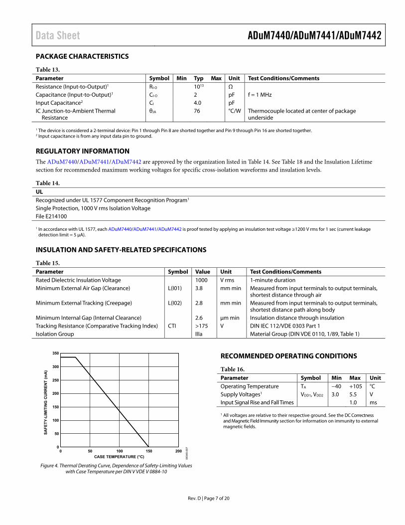
CASE TEMPERATURE (°C)
SAFE
TY-L
IMIT
ING
CU
RR
ENT
(mA
)
00
350
300
250
200
150
100
50
50 100 150 200
0834
0-00
7
Figure 4. Thermal Derating Curve, Dependence of Safety-Limiting Values
with Case Temperature per DIN V VDE V 0884-10
RECOMMENDED OPERATING CONDITIONS
Table 16. Parameter Symbol Min Max Unit Operating Temperature TA −40 +105 °C Supply Voltages1 VDD1, VDD2 3.0 5.5 V Input Signal Rise and Fall Times 1.0 ms 1 All voltages are relative to their respective ground. See the DC Correctness
and Magnetic Field Immunity section for information on immunity to external magnetic fields.

ADuM7440/ADuM7441/ADuM7442 Data Sheet
Rev. D | Page 8 of 20
ABSOLUTE MAXIMUM RATINGS TA = 25°C, unless otherwise noted.
Table 17. Parameter Rating Storage Temperature (TST) Range −65°C to +150°C Ambient Operating Temperature (TA) −40°C to +105°C Supply Voltages (VDD1, VDD2) −0.5 V to +7.0 V Input Voltages (VIA, VIB, VIC, VID)1, 2 −0.5 V to VDDI + 0.5 V Output Voltages (VOA, VOB, VOC, VOD)1, 2 −0.5 V to VDDO + 0.5 V Average Output Current per Pin3
Side 1 (IO1) −10 mA to +10 mA Side 2 (IO2) −10 mA to +10 mA
Common-Mode Transients3 −100 kV/μs to +100 kV/μs 1 VDDI and VDDO refer to the supply voltages on the input and output sides of a
given channel, respectively. See the Printed Circuit Board (PCB) Layout section. 2 See Figure 4 for maximum rated current values for various temperatures. 3 Refers to common-mode transients across the insulation barrier. Common-
mode transients exceeding the absolute maximum ratings may cause latch-up or permanent damage.
Stresses at or above those listed under Absolute Maximum Ratings may cause permanent damage to the product. This is a stress rating only; functional operation of the product at these or any other conditions above those indicated in the operational section of this specification is not implied. Operation beyond the maximum operating conditions for extended periods may affect product reliability.
ESD CAUTION
Table 18. Maximum Continuous Working Voltage1 Parameter Max Unit Constraint AC Voltage, Bipolar Waveform 420 V peak 50-year minimum lifetime
AC Voltage, Unipolar Waveform
Basic Insulation 420 V peak 50-year minimum lifetime
DC Voltage Basic Insulation 420 V peak 50-year minimum lifetime
1 Refers to continuous voltage magnitude imposed across the isolation barrier. See the Insulation Lifetime section for more details.
Table 19. Truth Table (Positive Logic) VIx Input1 VDDI State2 VDDO State3 VOx Output1 Description H Powered Powered H Normal operation; data is high. L Powered Powered L Normal operation; data is low. X Unpowered Powered H Input unpowered. Outputs are in the default high state. Outputs return to
input state within 1 μs of VDDI power restoration. See the pin function descriptions (Table 20 through Table 22) for more details.
X Powered Unpowered Z Output unpowered. Output pins are in high impedance state. Outputs return to input state within 1 μs of VDDO power restoration. See the pin function descriptions (Table 20 through Table 22) for more details.
1 VIx and VOx refer to the input and output signals of a given channel (A, B, C, or D). 2 VDDI refers to the power supply on the input side of a given channel (A, B, C, or D). 3 VDDO refers to the power supply on the output side of a given channel (A, B, C, or D).
Data Sheet ADuM7440/ADuM7441/ADuM7442
Rev. D | Page 9 of 20
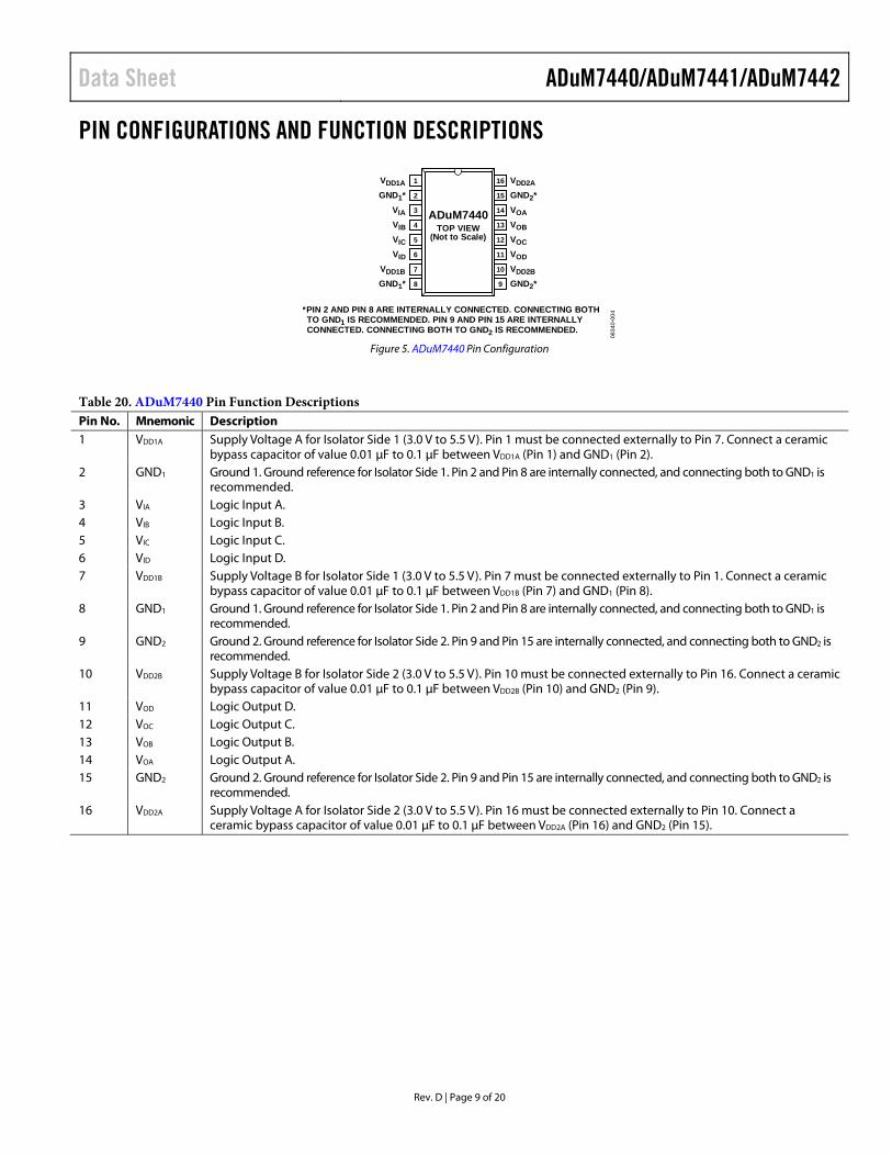
PIN CONFIGURATIONS AND FUNCTION DESCRIPTIONS
VDD1A 1
GND1* 2
VIA 3
VIB 4
VDD2A16
GND2*15
VOA14
VOB13
VIC 5 VOC12
VID 6 VOD11
VDD1B 7 VDD2B10
GND1* 8 GND2*9
ADuM7440TOP VIEW
(Not to Scale)
*PIN 2 AND PIN 8 ARE INTERNALLY CONNECTED. CONNECTING BOTHTO GND1 IS RECOMMENDED. PIN 9 AND PIN 15 ARE INTERNALLYCONNECTED. CONNECTING BOTH TO GND2 IS RECOMMENDED.
08
34
0-0
04
Figure 5. ADuM7440 Pin Configuration
Table 20. ADuM7440 Pin Function Descriptions Pin No. Mnemonic Description 1 VDD1A Supply Voltage A for Isolator Side 1 (3.0 V to 5.5 V). Pin 1 must be connected externally to Pin 7. Connect a ceramic
bypass capacitor of value 0.01 μF to 0.1 μF between VDD1A (Pin 1) and GND1 (Pin 2). 2 GND1 Ground 1. Ground reference for Isolator Side 1. Pin 2 and Pin 8 are internally connected, and connecting both to GND1 is
recommended. 3 VIA Logic Input A. 4 VIB Logic Input B. 5 VIC Logic Input C. 6 VID Logic Input D. 7 VDD1B Supply Voltage B for Isolator Side 1 (3.0 V to 5.5 V). Pin 7 must be connected externally to Pin 1. Connect a ceramic
bypass capacitor of value 0.01 μF to 0.1 μF between VDD1B (Pin 7) and GND1 (Pin 8). 8 GND1 Ground 1. Ground reference for Isolator Side 1. Pin 2 and Pin 8 are internally connected, and connecting both to GND1 is
recommended. 9 GND2 Ground 2. Ground reference for Isolator Side 2. Pin 9 and Pin 15 are internally connected, and connecting both to GND2 is
recommended. 10 VDD2B Supply Voltage B for Isolator Side 2 (3.0 V to 5.5 V). Pin 10 must be connected externally to Pin 16. Connect a ceramic
bypass capacitor of value 0.01 μF to 0.1 μF between VDD2B (Pin 10) and GND2 (Pin 9). 11 VOD Logic Output D. 12 VOC Logic Output C. 13 VOB Logic Output B. 14 VOA Logic Output A. 15 GND2 Ground 2. Ground reference for Isolator Side 2. Pin 9 and Pin 15 are internally connected, and connecting both to GND2 is
recommended. 16 VDD2A Supply Voltage A for Isolator Side 2 (3.0 V to 5.5 V). Pin 16 must be connected externally to Pin 10. Connect a
ceramic bypass capacitor of value 0.01 μF to 0.1 μF between VDD2A (Pin 16) and GND2 (Pin 15).

ADuM7440/ADuM7441/ADuM7442 Data Sheet
Rev. D | Page 10 of 20
VDD1A 1
GND1* 2
VIA 3
VIB 4
VDD2A16
GND2*15
VOA14
VOB13
VIC 5 VOC12
VOD 6 VID11
VDD1B 7 VDD2B10
GND1* 8 GND2*9
ADuM7441TOP VIEW
(Not to Scale)
*PIN 2 AND PIN 8 ARE INTERNALLY CONNECTED. CONNECTING BOTHTO GND1 IS RECOMMENDED. PIN 9 AND PIN 15 ARE INTERNALLYCONNECTED. CONNECTING BOTH TO GND2 IS RECOMMENDED.
08
34
0-0
05
Figure 6. ADuM7441 Pin Configuration
Table 21. ADuM7441 Pin Function Descriptions Pin No. Mnemonic Description 1 VDD1A Supply Voltage A for Isolator Side 1 (3.0 V to 5.5 V). Pin 1 must be connected externally to Pin 7. Connect a ceramic
bypass capacitor of value 0.01 μF to 0.1 μF between VDD1A (Pin 1) and GND1 (Pin 2). 2 GND1 Ground 1. Ground reference for Isolator Side 1. Pin 2 and Pin 8 are internally connected, and connecting both to GND1 is
recommended. 3 VIA Logic Input A. 4 VIB Logic Input B. 5 VIC Logic Input C. 6 VOD Logic Output D. 7 VDD1B Supply Voltage B for Isolator Side 1 (3.0 V to 5.5 V). Pin 7 must be connected externally to Pin 1. Connect a ceramic
bypass capacitor of value 0.01 μF to 0.1 μF between VDD1B (Pin 7) and GND1 (Pin 8). 8 GND1 Ground 1. Ground reference for Isolator Side 1. Pin 2 and Pin 8 are internally connected, and connecting both to GND1 is
recommended. 9 GND2 Ground 2. Ground reference for Isolator Side 2. Pin 9 and Pin 15 are internally connected, and connecting both to GND2 is
recommended. 10 VDD2B Supply Voltage B for Isolator Side 2 (3.0 V to 5.5 V). Pin 10 must be connected externally to Pin 16. Connect a ceramic
bypass capacitor of value 0.01 μF to 0.1 μF between VDD2B (Pin 10) and GND2 (Pin 9). 11 VID Logic Input D. 12 VOC Logic Output C. 13 VOB Logic Output B. 14 VOA Logic Output A. 15 GND2 Ground 2. Ground reference for Isolator Side 2. Pin 9 and Pin 15 are internally connected, and connecting both to GND2 is
recommended. 16 VDD2A Supply Voltage A for Isolator Side 2 (3.0 V to 5.5 V). Pin 16 must be connected externally to Pin 10. Connect a
ceramic bypass capacitor of value 0.01 μF to 0.1 μF between VDD2A (Pin 16) and GND2 (Pin 15).

Data Sheet ADuM7440/ADuM7441/ADuM7442
Rev. D | Page 11 of 20
VDD1A 1
GND1* 2
VIA 3
VIB 4
VDD2A16
GND2*15
VOA14
VOB13
VOC 5 VIC12
VOD 6 VID11
VDD1B 7 VDD2B10
GND1* 8 GND2*9
ADuM7442TOP VIEW
(Not to Scale)
*PIN 2 AND PIN 8 ARE INTERNALLY CONNECTED. CONNECTING BOTHTO GND1 IS RECOMMENDED. PIN 9 AND PIN 15 ARE INTERNALLYCONNECTED. CONNECTING BOTH TO GND2 IS RECOMMENDED.
0834
0-00
6
Figure 7. ADuM7442 Pin Configuration
Table 22. ADuM7442 Pin Function Descriptions Pin No. Mnemonic Description 1 VDD1A Supply Voltage A for Isolator Side 1 (3.0 V to 5.5 V). Pin 1 must be connected externally to Pin 7. Connect a ceramic
bypass capacitor of value 0.01 μF to 0.1 μF between VDD1A (Pin 1) and GND1 (Pin 2). 2 GND1 Ground 1. Ground reference for Isolator Side 1. Pin 2 and Pin 8 are internally connected, and connecting both to GND1 is
recommended. 3 VIA Logic Input A. 4 VIB Logic Input B. 5 VOC Logic Output C. 6 VOD Logic Output D. 7 VDD1B Supply Voltage B for Isolator Side 1 (3.0 V to 5.5 V). Pin 7 must be connected externally to Pin 1. Connect a ceramic
bypass capacitor of value 0.01 μF to 0.1 μF between VDD1B (Pin 7) and GND1 (Pin 8). 8 GND1 Ground 1. Ground reference for Isolator Side 1. Pin 2 and Pin 8 are internally connected, and connecting both to GND1 is
recommended. 9 GND2 Ground 2. Ground reference for Isolator Side 2. Pin 9 and Pin 15 are internally connected, and connecting both to GND2 is
recommended. 10 VDD2B Supply Voltage B for Isolator Side 2 (3.0 V to 5.5 V). Pin 10 must be connected externally to Pin 16. Connect a ceramic
bypass capacitor of value 0.01 μF to 0.1 μF between VDD2B (Pin 10) and GND2 (Pin 9). 11 VID Logic Input D. 12 VIC Logic Input C. 13 VOB Logic Output B. 14 VOA Logic Output A. 15 GND2 Ground 2. Ground reference for Isolator Side 2. Pin 9 and Pin 15 are internally connected, and connecting both to GND2 is
recommended. 16 VDD2A Supply Voltage A for Isolator Side 2 (3.0 V to 5.5 V). Pin 16 must be connected externally to Pin 10. Connect a
ceramic bypass capacitor of value 0.01 μF to 0.1 μF between VDD2A (Pin 16) and GND2 (Pin 15).

ADuM7440/ADuM7441/ADuM7442 Data Sheet
Rev. D | Page 12 of 20
TYPICAL PERFORMANCE CHARACTERISTICS
0834
0-01
50 5 10 15 20 25 30
DATA RATE (Mbps)
3V
5V
10
8
6
4
2
0
CU
RR
ENT
(mA
)
Figure 8. Typical Supply Current per Input Channel vs. Data Rate for 5 V and 3 V Operation
0834
0-01
6
CU
RR
ENT
(mA
)
0
1
2
3
4
0 5 10 15 20 25 30
DATA RATE (Mbps)
5V
3V
Figure 9. Typical Supply Current per Output Channel vs. Data Rate
for 5 V and 3 V Operation (No Output Load)
0834
0-01
7
CU
RR
ENT
(mA
)
0
1
2
3
4
0 5 10 15 20 25 30
DATA RATE (Mbps)
5V
3V
Figure 10. Typical Supply Current per Output Channel vs. Data Rate for 5 V and 3 V Operation (15 pF Output Load)
0834
0-01
8
CU
RR
ENT
(mA
)
0
5
10
15
20
25
30
35
0 5 10 15 20 25 30
DATA RATE (Mbps)
5V
3V
Figure 11. Typical ADuM7440 VDD1 Supply Current vs. Data Rate for 5 V and 3 V Operation
0834
0-01
9
CU
RR
ENT
(mA
)
0 5 10 15 20 25 30
DATA RATE (Mbps)
0
2
4
6
8
10
5V
3V
Figure 12. Typical ADuM7440 VDD2 Supply Current vs. Data Rate
for 5 V and 3 V Operation
0834
0-02
0
CU
RR
ENT
(mA
)
0 5 10 15 20 25 30
DATA RATE (Mbps)
5V
3V
0
5
10
15
20
25
30
35
Figure 13. Typical ADuM7441 VDD1 Supply Current vs. Data Rate
for 5 V and 3 V Operation

Data Sheet ADuM7440/ADuM7441/ADuM7442
Rev. D | Page 13 of 20
0834
0-02
1
CU
RR
ENT
(mA
)
0 5 10 15 20 25 30
DATA RATE (Mbps)
0
2
4
6
8
10
5V
3V
Figure 14. Typical ADuM7441 VDD2 Supply Current vs. Data Rate
for 5 V and 3 V Operation
0834
0-02
2
CU
RR
ENT
(mA
)
0 5 10 15 20 25 30
DATA RATE (Mbps)
0
5
10
15
20
25
5V
3V
Figure 15. Typical ADuM7442 VDD1 or VDD2 Supply Current vs. Data Rate
for 5 V and 3 V Operation
ADuM7440/ADuM7441/ADuM7442 Data Sheet
Rev. D | Page 14 of 20
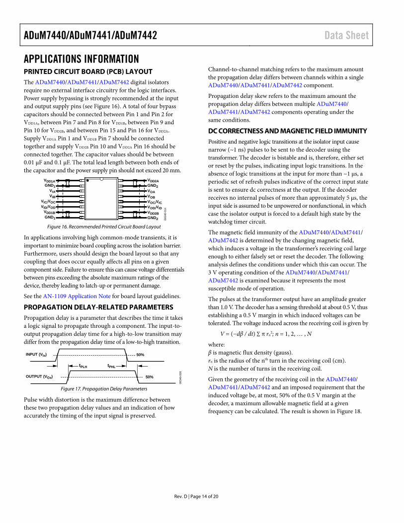
APPLICATIONS INFORMATION PRINTED CIRCUIT BOARD (PCB) LAYOUT The ADuM7440/ADuM7441/ADuM7442 digital isolators require no external interface circuitry for the logic interfaces. Power supply bypassing is strongly recommended at the input and output supply pins (see Figure 16). A total of four bypass capacitors should be connected between Pin 1 and Pin 2 for VDD1A, between Pin 7 and Pin 8 for VDD1B, between Pin 9 and Pin 10 for VDD2B, and between Pin 15 and Pin 16 for VDD2A. Supply VDD1A Pin 1 and VDD1B Pin 7 should be connected together and supply VDD2B Pin 10 and VDD2A Pin 16 should be connected together. The capacitor values should be between 0.01 μF and 0.1 μF. The total lead length between both ends of the capacitor and the power supply pin should not exceed 20 mm.
VDD1AGND1
VIAVIB
VIC/VOCVID/VOD
VDD1BGND1
VDD2AGND2VOAVOBVOC/VICVOD/VIDVDD2BGND2 0
8340
-014
Figure 16. Recommended Printed Circuit Board Layout
In applications involving high common-mode transients, it is important to minimize board coupling across the isolation barrier. Furthermore, users should design the board layout so that any coupling that does occur equally affects all pins on a given component side. Failure to ensure this can cause voltage differentials between pins exceeding the absolute maximum ratings of the device, thereby leading to latch-up or permanent damage.
See the AN-1109 Application Note for board layout guidelines.
PROPAGATION DELAY-RELATED PARAMETERS Propagation delay is a parameter that describes the time it takes a logic signal to propagate through a component. The input-to-output propagation delay time for a high-to-low transition may differ from the propagation delay time of a low-to-high transition.
INPUT (VIx)
OUTPUT (VOx)
tPLH tPHL
50%
50%
083
40
-00
8
Figure 17. Propagation Delay Parameters
Pulse width distortion is the maximum difference between these two propagation delay values and an indication of how accurately the timing of the input signal is preserved.
Channel-to-channel matching refers to the maximum amount the propagation delay differs between channels within a single ADuM7440/ADuM7441/ADuM7442 component.
Propagation delay skew refers to the maximum amount the propagation delay differs between multiple ADuM7440/ ADuM7441/ADuM7442 components operating under the same conditions.
DC CORRECTNESS AND MAGNETIC FIELD IMMUNITY Positive and negative logic transitions at the isolator input cause narrow (~1 ns) pulses to be sent to the decoder using the transformer. The decoder is bistable and is, therefore, either set or reset by the pulses, indicating input logic transitions. In the absence of logic transitions at the input for more than ~1 μs, a periodic set of refresh pulses indicative of the correct input state is sent to ensure dc correctness at the output. If the decoder receives no internal pulses of more than approximately 5 μs, the input side is assumed to be unpowered or nonfunctional, in which case the isolator output is forced to a default high state by the watchdog timer circuit.
The magnetic field immunity of the ADuM7440/ADuM7441/ ADuM7442 is determined by the changing magnetic field, which induces a voltage in the transformer’s receiving coil large enough to either falsely set or reset the decoder. The following analysis defines the conditions under which this can occur. The 3 V operating condition of the ADuM7440/ADuM7441/ ADuM7442 is examined because it represents the most susceptible mode of operation.
The pulses at the transformer output have an amplitude greater than 1.0 V. The decoder has a sensing threshold at about 0.5 V, thus establishing a 0.5 V margin in which induced voltages can be tolerated. The voltage induced across the receiving coil is given by
V = (−dβ / dt) ∑ π rn2; n = 1, 2, … , N
where: β is magnetic flux density (gauss). rn is the radius of the nth turn in the receiving coil (cm). N is the number of turns in the receiving coil.
Given the geometry of the receiving coil in the ADuM7440/ ADuM7441/ADuM7442 and an imposed requirement that the induced voltage be, at most, 50% of the 0.5 V margin at the decoder, a maximum allowable magnetic field at a given frequency can be calculated. The result is shown in Figure 18.

Data Sheet ADuM7440/ADuM7441/ADuM7442
Rev. D | Page 15 of 20
1000
100
10
1
0.1
0.01
0.0011k 100M10kM
AXI
MU
M A
LLO
WA
BLE
MA
GN
ETIC
FLU
X (k
gaus
s)
100k 1M 10MMAGNETIC FIELD FREQUENCY (Hz) 08
340-
009
Figure 18. Maximum Allowable External Magnetic Flux Density
For example, at a magnetic field frequency of 1 MHz, the maximum allowable magnetic field of 0.5 kgauss induces a voltage of 0.25 V at the receiving coil. This is about 50% of the sensing threshold and does not cause a faulty output transition. Similarly, if such an event occurred during a transmitted pulse (and was of the worst-case polarity), it would reduce the received pulse from >1.0 V to 0.75 V, still well above the 0.5 V sensing threshold of the decoder.
The preceding magnetic flux density values correspond to specific current magnitudes at given distances from the ADuM7440/ADuM7441/ADuM7442 transformers. Figure 19 shows these allowable current magnitudes as a function of frequency for selected distances. As shown, the ADuM7440/ ADuM7441/ADuM7442 are extremely immune and can be affected only by extremely large currents operated at high frequency very close to the component. For the 1 MHz example noted previously, a 1.2 kA current would have to be placed 5 mm away from the ADuM7440/ADuM7441/ADuM7442 to affect the operation of the component.
1000
100
10
1
0.1
0.011k 100M10k
MA
XIM
UM
ALL
OW
AB
LE C
UR
REN
T (k
A)
100k 1M 10MMAGNETIC FIELD FREQUENCY (Hz)
DISTANCE = 5mmDISTANCE = 100mmDISTANCE = 1m
0834
0-01
0
Figure 19. Maximum Allowable Current for Various
Current-to-ADuM7440/ADuM7441/ADuM7442 Spacings
Note that at combinations of strong magnetic field and high frequency, any loops formed by printed circuit board traces can induce error voltages sufficiently large enough to trigger the thresholds of succeeding circuitry. Take care in the layout of such traces to avoid this possibility.
POWER CONSUMPTION The supply current at a given channel of the ADuM7440/ ADuM7441/ADuM7442 isolator is a function of the supply voltage, the data rate of the channel, and the output load of the channel.
For each input channel, the supply current is given by
IDDI = IDDI (Q) f ≤ 0.5 fr
IDDI = IDDI (D) × (2f − fr) + IDDI (Q) f > 0.5 fr
For each output channel, the supply current is given by
IDDO = IDDO (Q) f ≤ 0.5 fr
IDDO = (IDDO (D) + (0.5 × 10⁻³) × CL × VDDO) × (2f − fr) + IDDO (Q)
f > 0.5 fr
where: IDDI (D), IDDO (D) are the input and output dynamic supply currents per channel (mA/Mbps). CL is the output load capacitance (pF). VDDO is the output supply voltage (V). f is the input logic signal frequency (MHz); it is half the input data rate, expressed in Mbps. fr is the input stage refresh rate (Mbps). IDDI (Q), IDDO (Q) are the specified input and output quiescent supply currents (mA).
To calculate the total VDD1 and VDD2 supply current, the supply currents for each input and output channel corresponding to VDD1 and VDD2 are calculated and totaled. Figure 8 and Figure 9 show per-channel supply currents as a function of data rate for an unloaded output condition. Figure 10 shows the per-channel supply current as a function of data rate for a 15 pF output condition. Figure 11 through Figure 15 show the total VDD1 and VDD2 supply current as a function of data rate for ADuM7440/ ADuM7441/ADuM7442 channel configurations.
INSULATION LIFETIME All insulation structures eventually break down when subjected to voltage stress over a sufficiently long period. The rate of insulation degradation is dependent on the characteristics of the voltage waveform applied across the insulation. In addition to the testing performed by the regulatory agencies, Analog Devices carries out an extensive set of evaluations to determine the lifetime of the insulation structure within the ADuM7440/ ADuM7441/ADuM7442.
Analog Devices performs accelerated life testing using voltage levels higher than the rated continuous working voltage. Acceleration factors for several operating conditions are determined. These factors allow calculation of the time to failure at the actual working voltage. The values shown in Table 18 summarize the peak voltage for 50 years of service life for a bipolar ac operating condition and the maximum CSA approved working voltages. In many cases, the approved working voltage is higher than 50-year service life voltage. Operation at these high working voltages can lead to shortened insulation life in some cases.
ADuM7440/ADuM7441/ADuM7442 Data Sheet
Rev. D | Page 16 of 20
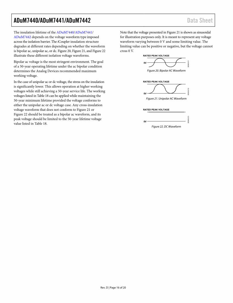
The insulation lifetime of the ADuM7440/ADuM7441/ ADuM7442 depends on the voltage waveform type imposed across the isolation barrier. The iCoupler insulation structure degrades at different rates depending on whether the waveform is bipolar ac, unipolar ac, or dc. Figure 20, Figure 21, and Figure 22 illustrate these different isolation voltage waveforms.
Bipolar ac voltage is the most stringent environment. The goal of a 50-year operating lifetime under the ac bipolar condition determines the Analog Devices recommended maximum working voltage.
In the case of unipolar ac or dc voltage, the stress on the insulation is significantly lower. This allows operation at higher working voltages while still achieving a 50-year service life. The working voltages listed in Table 18 can be applied while maintaining the 50-year minimum lifetime provided the voltage conforms to either the unipolar ac or dc voltage case. Any cross-insulation voltage waveform that does not conform to Figure 21 or Figure 22 should be treated as a bipolar ac waveform, and its peak voltage should be limited to the 50-year lifetime voltage value listed in Table 18.
Note that the voltage presented in Figure 21 is shown as sinusoidal for illustration purposes only. It is meant to represent any voltage waveform varying between 0 V and some limiting value. The limiting value can be positive or negative, but the voltage cannot cross 0 V.
0V
RATED PEAK VOLTAGE
0834
0-01
1
Figure 20. Bipolar AC Waveform
0V
RATED PEAK VOLTAGE
0834
0-01
2
Figure 21. Unipolar AC Waveform
0V
RATED PEAK VOLTAGE
0834
0-01
3
Figure 22. DC Waveform
Data Sheet ADuM7440/ADuM7441/ADuM7442
Rev. D | Page 17 of 20
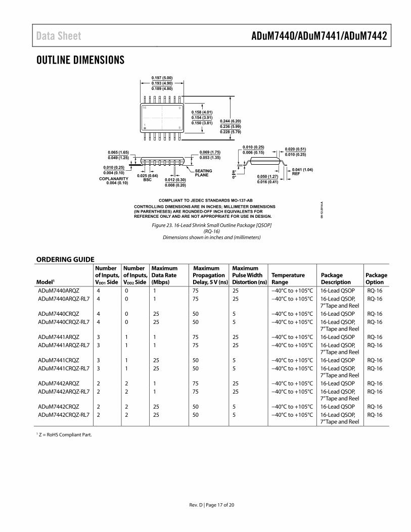
OUTLINE DIMENSIONS
COMPLIANT TO JEDEC STANDARDS MO-137-ABCONTROLLING DIMENSIONS ARE IN INCHES; MILLIMETER DIMENSIONS(IN PARENTHESES) ARE ROUNDED-OFF INCH EQUIVALENTS FORREFERENCE ONLY AND ARE NOT APPROPRIATE FOR USE IN DESIGN.
16 9
81
SEATINGPLANE
0.010 (0.25)0.004 (0.10)
0.012 (0.30)0.008 (0.20)
0.025 (0.64)BSC
0.041 (1.04)REF
0.010 (0.25)0.006 (0.15)
0.050 (1.27)0.016 (0.41)
0.020 (0.51)0.010 (0.25)
8°0°COPLANARITY
0.004 (0.10)
0.065 (1.65)0.049 (1.25)
0.069 (1.75)0.053 (1.35)
0.197 (5.00)0.193 (4.90)0.189 (4.80)
0.158 (4.01)0.154 (3.91)0.150 (3.81) 0.244 (6.20)
0.236 (5.99)0.228 (5.79)
09-1
2-20
14-A
Figure 23. 16-Lead Shrink Small Outline Package [QSOP]
(RQ-16) Dimensions shown in inches and (millimeters)
ORDERING GUIDE
Model1
Number of Inputs, VDD1 Side
Number of Inputs, VDD2 Side
Maximum Data Rate (Mbps)
Maximum Propagation Delay, 5 V (ns)
Maximum Pulse Width Distortion (ns)
Temperature Range
Package Description
Package Option
ADuM7440ARQZ 4 0 1 75 25 −40°C to +105°C 16-Lead QSOP RQ-16 ADuM7440ARQZ-RL7 4 0 1 75 25 −40°C to +105°C 16-Lead QSOP,
7” Tape and Reel RQ-16
ADuM7440CRQZ 4 0 25 50 5 −40°C to +105°C 16-Lead QSOP RQ-16 ADuM7440CRQZ-RL7 4 0 25 50 5 −40°C to +105°C 16-Lead QSOP,
7” Tape and Reel RQ-16
ADuM7441ARQZ 3 1 1 75 25 −40°C to +105°C 16-Lead QSOP RQ-16 ADuM7441ARQZ-RL7 3 1 1 75 25 −40°C to +105°C 16-Lead QSOP,
7” Tape and Reel RQ-16
ADuM7441CRQZ 3 1 25 50 5 −40°C to +105°C 16-Lead QSOP RQ-16 ADuM7441CRQZ-RL7 3 1 25 50 5 −40°C to +105°C 16-Lead QSOP,
7” Tape and Reel RQ-16
ADuM7442ARQZ 2 2 1 75 25 −40°C to +105°C 16-Lead QSOP RQ-16 ADuM7442ARQZ-RL7 2 2 1 75 25 −40°C to +105°C 16-Lead QSOP,
7” Tape and Reel RQ-16
ADuM7442CRQZ 2 2 25 50 5 −40°C to +105°C 16-Lead QSOP RQ-16 ADuM7442CRQZ-RL7 2 2 25 50 5 −40°C to +105°C 16-Lead QSOP,
7” Tape and Reel RQ-16
1 Z = RoHS Compliant Part.

ADuM7440/ADuM7441/ADuM7442 Data Sheet
Rev. D | Page 18 of 20
NOTES

Data Sheet ADuM7440/ADuM7441/ADuM7442
Rev. D | Page 19 of 20
NOTES
ADuM7440/ADuM7441/ADuM7442 Data Sheet
Rev. D | Page 20 of 20
NOTES
©2009–2015 Analog Devices, Inc. All rights reserved. Trademarks and registered trademarks are the property of their respective owners. D08340-0-10/15(D)