1 m. kirchgessner twepp, 24.09.2014 manfred kirchgessner on behalf of the dssc collaboration dssc =...
TRANSCRIPT

1
M. KirchgessnerTWEPP, 24.09.2014
High performance readout chain for the DSSC 1M Pixel detector, designed for high throughput during
pulsed operation mode
Topical Workshop on Electronics for Particle PhysicsAix en Provence, 24.09.2014
Manfred Kirchgessner on behalf of the DSSC Collaboration
DSSC = DEPFET Sensor with Signal Compression

2
M. KirchgessnerTWEPP, 24.09.2014
The European XFEL
DSSC system overview
Readout chain implementation
Implementation details
Summary
Outline

3
M. KirchgessnerTWEPP, 24.09.2014
The European XFEL

4
M. KirchgessnerTWEPP, 24.09.2014
EuXFEL construction site at Hamburg
Three 2D detector developments at the European XFEL(coordinator: M. Kuster)
Adaptive Gain integrating Pixel Detector Consortium (AGIPD)(Project Leader: H. Graafsma)
Large Pixel Detector Consortium (LPD)(Project Leader: M. French)
DEPFET Sensor with Signal Compression Consortium (DSSC) (Project Leader: M. Porro)

5
M. KirchgessnerTWEPP, 24.09.2014
EuXFEL – bunch structure
readout
The EuXFEL runs in pulsed operation mode:
Bunch repetition rate of 10 Hz
Sequences of ~2700 pulses
Up to min 220 ns distance
(frame rate 4.5 MHz)
~100 fs wide X-Ray pulses
(exposure time)
99.4 ms pause between macro
bunches
Max frame rate:
4.5 MHz
Data readout

6
M. KirchgessnerTWEPP, 24.09.2014
The DSSC Detector

7
M. KirchgessnerTWEPP, 24.09.2014
Sensor and focal plane architecture
DEPFET with non linear characteristic• Silicon detector with internal gate• Intrinsic low noise due to small internal gate
capacitance• Intrinsic signal compression
Focal Plane composition• 1024x1024 pixels• 32 monolithic sensors • Sensor bump bonded to 8 Readout ASICs • Dead area: ~15%
Power cycling• 10.7 kW peak power• 240 W average power
Readout concept• Full parallel readout• Analogue shaping using trapezoidal filter• In-Pixel 9 Bit ADC • In-Pixel SRAM Memory ( 800 frames ) Focal-Plane
248x240mm
© Image by Karsten Hansen

8
M. KirchgessnerTWEPP, 24.09.2014
DSSC – Design Parameters
General Parameters
Energy range optimized for 0.5 … 6 keV
Number of pixels 1024 x 1024
Sensor Pixel Shape Hexagonal
Sensor Pixel pitch ~ 204 x 236 µm2
Dynamic range / pixel / pulse
~5000 ph @ 0.5 keV> 10000 ph @ E≥1 keV
Resolution Single photon detection also @ 0.25 keV
Frame rate 0.9 - 4.5 MHzStored frames per Macro bunch 800
Operating temperature
-20˚C optimum, RT possible

9
M. KirchgessnerTWEPP, 24.09.2014
The DSSC high throughput readout
chain

10
M. KirchgessnerTWEPP, 24.09.2014
DSSC Ladder components
Monolithic DEPFET sensor
Mainboard
Module-Interconnection Board: MIB
Power Regulator Board
Patch-Panel Flex CableReadout ASIC
I/O Board ( 1st FPGA stage)
Module-Interconnection Board

11
M. KirchgessnerTWEPP, 24.09.2014
THE DSSC System overview
© Image by Karsten Hansen
Second FPGA Stage
1MPixel x 800 images x 2 Bytes per Pixel
= 1600 MByte per 0.1 seconds
Total data production rate of the detector:
128 GBit/sor 32 GBit/s per PPT

12
M. KirchgessnerTWEPP, 24.09.2014
DSSC DAQ Architecture

13
M. KirchgessnerTWEPP, 24.09.2014
DSSC DAQ Architecture – ASIC
Readout ASIC:
• IBM 130nm technology
• 4096 pixels per ASIC
• In-Pixel SRAM cells for 800 9 bit words
• One 10 bit serializer running at 350 MHz (400 MHz also successfully tested)
9 bit data + 1 bit parity
14
M. KirchgessnerTWEPP, 24.09.2014
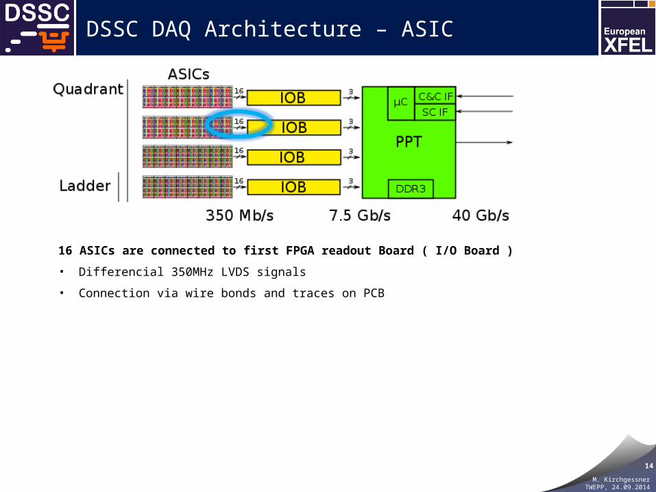
DSSC DAQ Architecture – ASIC
16 ASICs are connected to first FPGA readout Board ( I/O Board )
• Differencial 350MHz LVDS signals
• Connection via wire bonds and traces on PCB

15
M. KirchgessnerTWEPP, 24.09.2014
DSSC DAQ Architecture – I/O Board
I/O Board implements the first FPGA stage
• FPGA: Spartan 6 LX 45 (xc6slx45t-3-csg324)
• Combines the data from 16 ASICs into one data stream
• Implements 3 high speed serial Xilinx Aurora links
• Additional capacitors for pulsed sensor supply
• Temperature sensor
16
M. KirchgessnerTWEPP, 24.09.2014
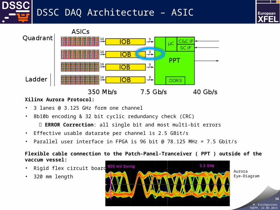
DSSC DAQ Architecture – ASIC
Xilinx Aurora Protocol:
• 3 lanes @ 3.125 GHz form one channel
• 8b10b encoding & 32 bit cyclic redundancy check (CRC)
ERROR Correction: all single bit and most multi-bit errors
• Effective usable datarate per channel is 2.5 GBit/s
• Parallel user interface in FPGA is 96 bit @ 78.125 MHz = 7.5 Gbit/s
Flexible cable connection to the Patch-Panel-Tranceiver ( PPT ) outside of the vaccum vessel:
• Rigid flex circuit board
• 320 mm length AuroraEye-Diagram

17
M. KirchgessnerTWEPP, 24.09.2014
DSSC DAQ Architecture – PPT
The Patch-Panel-Tranceiver ( PPT ) implements the main FPGA stage
• FPGA: Kintex 7 325T (xc7k325t-ffg900-2)
• Receives data from 4 IOBoards over 4 x 3 lanes = 12 Aurora lanes
• 1 GByte high speed DDR3-1600 data buffer
• 4 x 10 GBit/s ethernet links that connect to a QSFP 40Gb/s
• Microblaze µC with an embedded linux for slow control via 1GBit/s ethernet

18
M. KirchgessnerTWEPP, 24.09.2014
PPT Firmware Details

19
M. KirchgessnerTWEPP, 24.09.2014
PPT FPGA Firmware – Datarates
Data Input22.4 Gbit/s
¿𝟑𝟐𝑮𝑩𝒊𝒕 /𝒔

20
M. KirchgessnerTWEPP, 24.09.2014
Implementation Details

21
M. KirchgessnerTWEPP, 24.09.2014
PPT – FPGA Connections
1GB DDR3-1600
Rx-Aurora
QSFP
Detector Slow-Control
DDR3-800µC
FPGA Connections Kintex 7 325T

22
M. KirchgessnerTWEPP, 24.09.2014
Aurora - implementation details
Aurora IP-core details:
Simplex core implemented (no back channel)
Streaming interface for easy data transmition
Timer used for initialization sequence
Only one differencial wire pair per lane between FPGAs required
License comes with ISE
MGT usage:
One input clock can be connected to 3 GTX Quads.
Each GTX transceiver can be driven by ist own PLL (CPLL) or by the QuadPLL
• CPLL (in each GTX Channel included) for linerates 1.6 – 3.3 Gbit/s
(connected in Aurora)
• QPLL (one per Quad) for linerates 5.93 – 12.5 Gbit/s
• (required for 10GigE)
Each Aurora channel is distributed to 3 Quads – 1 Lane per Quad
Signal quality can be improved by optimizing swing and pre-emphasys settings
GTP Quad Chan1
Chan2
Chan3
Chan4
Chan1
Chan2
Chan3
Chan4
Chan1
Chan2
Chan3
Chan4

23
M. KirchgessnerTWEPP, 24.09.2014
DDR3 1600 - implementation details
IP-Core Version:
Xilinx DRAM-controller mig 7 v1.9
License comes with ISE
Interface:
4 DDR3 modules with 16 bit width = 64 bit data bus @ 800 MHz
On the firmware (user) side: 512 bit data bus @ 200 MHz single data rate
Running in burst mode of up to 256 words x 512 bits.
Alternating read and write bursts to minimize latency
• In alternating read/write mode max bandwidth achieved is 88 GBit/s
24
M. KirchgessnerTWEPP, 24.09.2014
QSFP - implementation details
IP Core:
Adaptions required to support FOUR 10GigE channels, single links can directly be generated
Licence required
System Tests:
System was tested using a standard desktop PC
1 x 10GigE PCI-Express SFP receiver card (single link tested via breakout cable)
It is possible to receive 8kB UDP packets at ~10GBit/s without loss after some optimiziations:
• Linux driver adaptions of buffer sizes
• Move data-receiving in seperate CPU thread
• No data stored, just copied from buffer and checked

25
M. KirchgessnerTWEPP, 24.09.2014
PPT – board details
Board details:
~ 5000 € per Board
14 layers
Size: 80x160mm
Supplied by 12 volts / 17W
9 different supply levels: 12 Volts +
Booting and update:
Boot chain for successive power-up of all required voltages
FPGA & Linux boot automaticly from SPI-connected flash memory
• Firmware & Linux flash reprogrammable from Microblace
• Re-boot process triggerable from remote
• IO Board FPGAs programmed by PPT
After ~5 min system is ready
PPT top view
2 x 1.0V1.2V1.5V1.8V2.0V2.5V3.3V
Full system update possible from remote

26
M. KirchgessnerTWEPP, 24.09.2014
PPT – board details
Debugging:
Xilinx JTAG Programmer Cable for early debugging
Xilinx virtual cable implemented:
• Xilinx Chipscope access to all IOB FPGAs AND PPT FPGA remotely via ethernet
USB ftdi interface ( linux boot output )
PPT top view
Debug access available even when installed in vacuum

27
M. KirchgessnerTWEPP, 24.09.2014
Summary
Differential links LVDS @ 350MBit/s
Aurora protocol @ 3.125 GBit/s over 30cm LVDS on Flex-Cable runs reliable.
Aurora Lanes can be distributed to different GTX Quads
10 GBit/s link works nice at >90% speed.
DDR3 – 1600 @ 800 MHz works out of the box, if hardware timings are known.
Outlook:
First X-Ray beam 2015
First DSSC ladder camera (65k pixel) 2015
Full DSSC 1M pixel camera 2017
28
M. KirchgessnerTWEPP, 24.09.2014
M. Porro1, L. Andricek2, S. Aschauer3, M. Bayer4, A. Castoldi4,5, D. Comotti6, M. Donato7, F. Erdinger8, C. Fiorini4,5, P. Fischer8, H. Graafsma9, C. Guazzoni4,5, K. Hansen9, P. Kalavakuru9, H. Klaer9, M. Kirchgessner8, A. Kugel8, M. Kuster7, P. Lechner3, G. Lutz3, P. Majewski3, M. Manghisoni6, D. Moch1, B. Nasri4, S. Nidhi7, V. Re6, C. Reckleben9, R. Richter2, S. Schlee7, J. Soldat8, L. Strueder8, J. Szymanski9, M. Turcato7, G. Weidenspointner7, C. Wunderer9
1) Max Planck Institut fuer Extraterrestrische Physik, Garching, Germany2) MPG Halbleiterlabor, Muenchen, Germany3) PNSensor GmbH, Muenchen, Germany4) Dipartimento di Elettronica e Informazione, Politecnico di Milano, Milano, Italy5) Sezione di Milano, Italian National Institute of Nuclear Physics (INFN), Milano, Italy6) Dipartimento di ingegneria industriale, Università di Bergamo, Bergamo, Italy7) European XFEL GmbH, Hamburg, Germany8) Zentrales Institut für Technische Informatik, Universitaet Heidelberg, Heidelberg, Germany9) Deutsches Elektronen-Synchrotron DESY, Hamburg, Germany
The DSSC Consortium

29
M. KirchgessnerTWEPP, 24.09.2014
THANK YOU
for your attention

30
M. KirchgessnerTWEPP, 24.09.2014
PPT - FPGA Utilization
LOGIC Used Available Ratio
Slice Registers 77.228 407.600 18%
Slice LUTs 81.387 203.800 39%
Occupied slices 32.635 50.950 64%
RAMB36/FIFO36 115 445 25%
RAMB18/FIFO18 91 890 10%
GTXE2_CHANNELS 16 16 100%
FPGA: Kintex 7 325T (xc7k325t-ffg900-2)

31
M. KirchgessnerTWEPP, 24.09.2014
PPT – FPGA Logic distribution
Microblaze23%
DDR315%
10GBE x4 QSFP28%
Aurora x47%
Rest Datapath17%
Other10%
Logic

32
M. KirchgessnerTWEPP, 24.09.2014
Used IP Cores
● Used Xilinx IP cores + self written wrapper code (verilog)
Aurora 8B10B v8.3 Rx&Tx
FIFO Generator v9.3 (no wrapper required)
1GB DDR3-1600 memory controller MIG 7 Series 1.9
Ethernet MAC + PHY (v11.6 + PCS/PMA 2.6)
● Xilinx EDK was used to implement the Microblace
Running @ 100MHz
Running a busybox linux
Discrete 256 MB DDR3-800 DRAM controller
Gigabit ethernet controller
Only for slow control

33
M. KirchgessnerTWEPP, 24.09.2014
Kintex 7 GTX Quad - QPLL
Certain refclock frequency for application required

34
M. KirchgessnerTWEPP, 24.09.2014
ASIC
0.00 0.05 0.10 0.15 0.20 0.25 0.30 0.35 0.40 0.45
0.330.35
0.4
Maximum Implemented Min Required
Datarate [GBit/s]
DSSC– implemented datarates
IOB
0.00 1.25 2.50 3.75 5.00 6.25 7.50
5.275.6
7.5
Datarate [GBit/s]
QSFP
0.00 5.00 10.00 15.00 20.00 25.00 30.00 35.00 40.00 45.00
33.7635.84
40
Datarate [GBit/s]
DDR3Buffer (in+out)
0.00 15.00 30.00 45.00 60.00 75.00 90.00 105.00
67.5171.68
102.4
Datarate [GBit/s]