1. preamble - asti.edu.in · pdf filepower electronic simulation lab department of eee 1 astra...
TRANSCRIPT

Power Electronic Simulation Lab
Department of EEE 1 ASTRA
1. PREAMBLE
The significance of the power electronics Lab is renowned in the various fields of
engineering applications. For an Electrical Engineer, it is obligatory to have the practical
ideas about the power electronics Circuits. By this perspective we have introduced a
Laboratory manual cum Observation for power electronics.
The manual uses the plan, cogent and simple language to explain the fundamental aspects
of power electronics. The manual preparedvery carefully with our level best. It gives all the
steps in executing an experiment.

Power Electronic Simulation Lab
Department of EEE 2 ASTRA
2 OBJECTIVE & RELEVANCE
The objective of this Power Electronics laboratory is to study the characteristics of switching
devices and its applications in rectifier inverter, chopper and resonant converter. It also
introduces the application of electronic devices for conversion, control conditioning of
electric power. Further it helps the students to get an overview of different types of power
semi-conductor devices and their switching characteristics and to understand the operation,
characteristics and performance parameters of controlled rectifiers, to study the operation ,
switching techniques, modulation techniques of pulse width modulated inverters and to
understand the harmonic reduction method
OUTCOME:
After the completion of this course students are able to analyze the all types of converters by using simulation through PSPICE software
Understanding of all converters practically .
Applications of converters

Power Electronic Simulation Lab
Department of EEE 3 ASTRA
3 LIST OF EXPERIMENTS
1 Single phase ac voltage controller
2 Resonant pulse commutation circuit
3 Three phase full converter using rl&e loads
4 Impulse commutation circuit
5 Three phase inverter with pwm controller
6 Single phase full converter
7 Three phase half controlled bridge converter
8 Single phase cycloconverter
9 Single phase half controlled bridge converter
10 Single phase fully controlled bridge converter

Power Electronic Simulation Lab
Department of EEE 4 ASTRA
4 Text and Reference Books:
T1. M.D Singh & K.B. Kanchandhani “Power Electronics” Tata Mc Graw – Hill Publishing
Company, 2007
T2. M.H. Rashid “Power Electronics: Circuits, Devices and Applications” Prentice Hall of
India, 2nd
REFERENCE BOOKS
R1. Vedam Subramanyam “Power Electronics” New Age International (P) Limited,
Publishers.
R2 : V.R. Murthy “Power Electronics” 1st Edition 2005, Oxford University Press
R3 : P.C. Sen “Power Electronics” Tata Mc Graw-Hill Publishing
Power Electronic Simulation Lab
Department of EEE 5 ASTRA
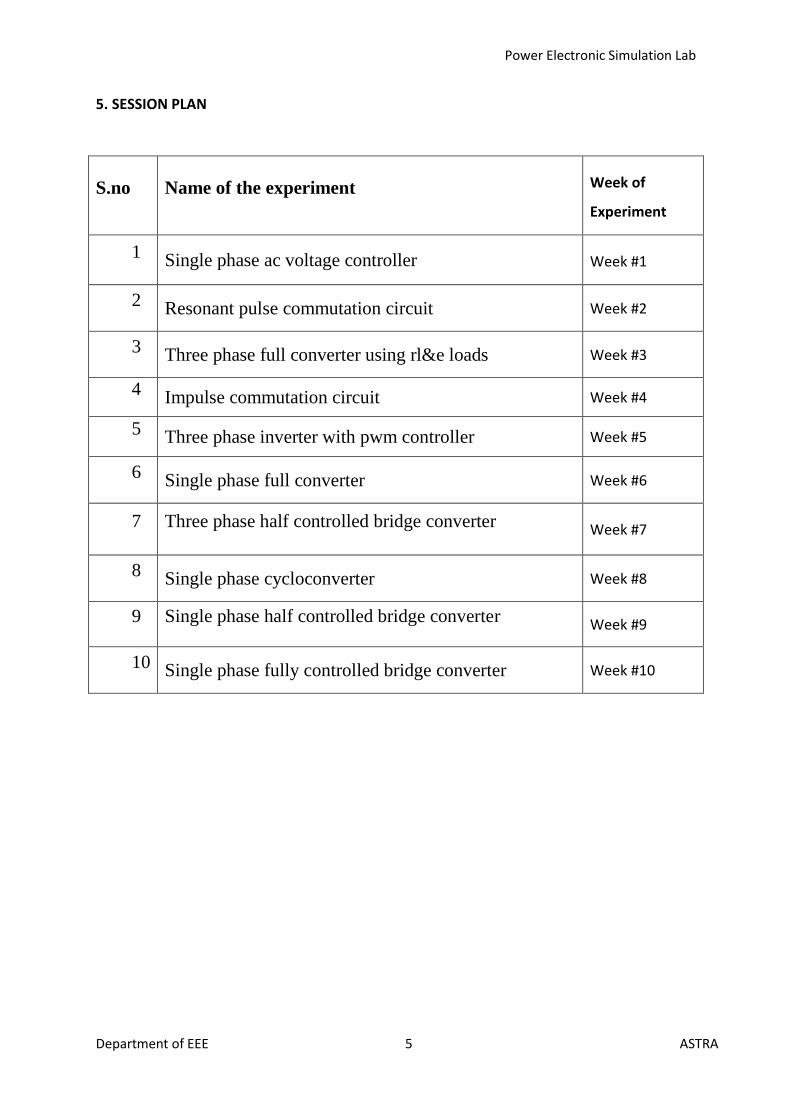
5. SESSION PLAN
S.no Name of the experiment Week of
Experiment
1 Single phase ac voltage controller Week #1
2 Resonant pulse commutation circuit Week #2
3 Three phase full converter using rl&e loads Week #3
4 Impulse commutation circuit Week #4
5 Three phase inverter with pwm controller Week #5
6 Single phase full converter Week #6
7 Three phase half controlled bridge converter Week #7
8 Single phase cycloconverter Week #8
9 Single phase half controlled bridge converter Week #9
10 Single phase fully controlled bridge converter Week #10

Power Electronic Simulation Lab
Department of EEE 6 ASTRA
6 Experiment write up
6.1 SINGLE PHASE AC VOLTAGE CONTROLLER
EXP NO:
Date:
Aim: To analyze the simulation of single phase ac voltage controller.
Software Required: PSPICE (Personal Computer Simulated Program with
Integrated Circuit Emphasis.
Program:
VS 1 0 SIN(0V 169.7V 60HZ)
VG1 2 4 PULSE(0V 10V 4166.7US 1NS 1NS 100US 16666.67US)
VG2 3 1 PULSE(0V 10V 12500.0US 1NS 1NS 100US 16666.67US)
R 4 5 2.5
L 5 6 6.5MH
VX 6 0 DC 0V
CS 1 7 0.1UF
RS 7 4 750
XT1 1 4 2 4 SCR
XT2 4 1 3 1 SCR
.SUBCKT SCR 1 2 3 2
S1 1 5 6 2 SMOD
RG 3 4 50
VX 4 2 DC 0V
VY 5 2 DC 0V
RT 2 6 1
CT 6 2 10UF
F1 2 6 POLY(2) VX VY 0 50 11
.MODEL SMOD VSWITCH(RON=0.01 ROFF=10E+5 VON=0.1V VOFF=0V)
.ENDS SCR
.TRAN 10US 33.33MS
.PROBE
.FOUR 60HZ V(4)
Power Electronic Simulation Lab
Department of EEE 7 ASTRA
.END
Result:

Power Electronic Simulation Lab
Department of EEE 8 ASTRA

Power Electronic Simulation Lab
Department of EEE 9 ASTRA
Output Waveforms:
Power Electronic Simulation Lab
Department of EEE 10 ASTRA
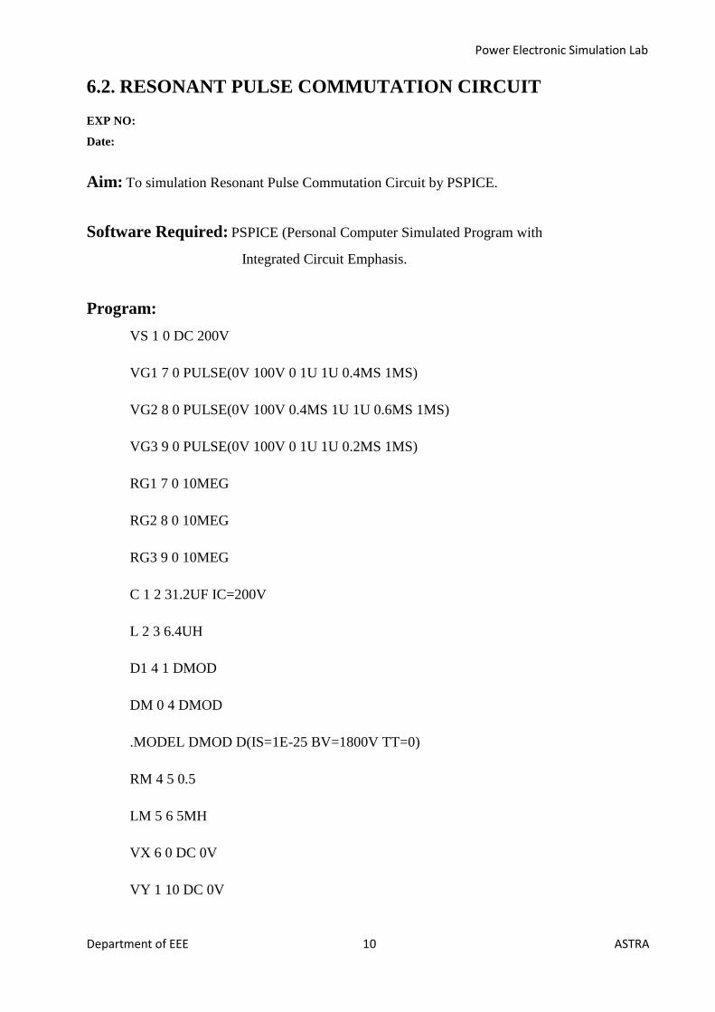
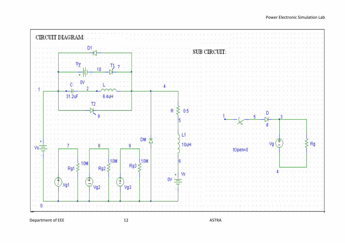
6.2. RESONANT PULSE COMMUTATION CIRCUIT
EXP NO:
Date:
Aim: To simulation Resonant Pulse Commutation Circuit by PSPICE.
Software Required: PSPICE (Personal Computer Simulated Program with
Integrated Circuit Emphasis.
Program:
VS 1 0 DC 200V
VG1 7 0 PULSE(0V 100V 0 1U 1U 0.4MS 1MS)
VG2 8 0 PULSE(0V 100V 0.4MS 1U 1U 0.6MS 1MS)
VG3 9 0 PULSE(0V 100V 0 1U 1U 0.2MS 1MS)
RG1 7 0 10MEG
RG2 8 0 10MEG
RG3 9 0 10MEG
C 1 2 31.2UF IC=200V
L 2 3 6.4UH
D1 4 1 DMOD
DM 0 4 DMOD
.MODEL DMOD D(IS=1E-25 BV=1800V TT=0)
RM 4 5 0.5
LM 5 6 5MH
VX 6 0 DC 0V
VY 1 10 DC 0V

Power Electronic Simulation Lab
Department of EEE 11 ASTRA
.SUBCKT DCSCR 1 2 3 4
DT 5 2 DMOD
ST 1 5 3 4 SMOD
.MODEL DMOD D(IS=1E-25 BV=1800V TT=0V)
.MODEL SMOD VSWITCH(RON=0.1 ROFF=10E+6 VON=10V VOFF=5V)
.ENDS DCSCR
XT1 10 4 7 0 DCSCR
XT2 3 4 8 0 DCSCR
XT3 1 3 9 0 DCSCR
.TRAN 0.5US 3MS 1.5MS 0.5US
.PROBE
.END
O/p Waveform Details: I(VX) --- Current Through Load Terminals .
I(C) ------ Current Through Capacitor.
V(1,2) --- Voltage Across the Capacitor.
Result: Analysis of Resonant Pulse Commutation has been successfully completed.
Power Electronic Simulation Lab
Department of EEE 12 ASTRA

Power Electronic Simulation Lab
Department of EEE 13 ASTRA
Output Waveforms:
Power Electronic Simulation Lab
Department of EEE 14 ASTRA
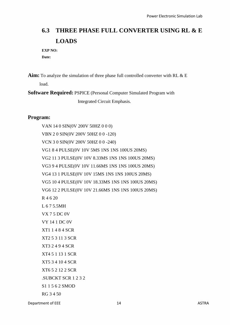
6.3 THREE PHASE FULL CONVERTER USING RL & E
LOADS
EXP NO:
Date:
Aim: To analyze the simulation of three phase full controlled converter with RL & E
load.
Software Required: PSPICE (Personal Computer Simulated Program with
Integrated Circuit Emphasis.
Program:
VAN 14 0 SIN(0V 200V 50HZ 0 0 0)
VBN 2 0 SIN(0V 200V 50HZ 0 0 -120)
VCN 3 0 SIN(0V 200V 50HZ 0 0 -240)
VG1 8 4 PULSE(0V 10V 5MS 1NS 1NS 100US 20MS)
VG2 11 3 PULSE(0V 10V 8.33MS 1NS 1NS 100US 20MS)
VG3 9 4 PULSE(0V 10V 11.66MS 1NS 1NS 100US 20MS)
VG4 13 1 PULSE(0V 10V 15MS 1NS 1NS 100US 20MS)
VG5 10 4 PULSE(0V 10V 18.33MS 1NS 1NS 100US 20MS)
VG6 12 2 PULSE(0V 10V 21.66MS 1NS 1NS 100US 20MS)
R 4 6 20
L 6 7 5.5MH
VX 7 5 DC 0V
VY 14 1 DC 0V
XT1 1 4 8 4 SCR
XT2 5 3 11 3 SCR
XT3 2 4 9 4 SCR
XT4 5 1 13 1 SCR
XT5 3 4 10 4 SCR
XT6 5 2 12 2 SCR
.SUBCKT SCR 1 2 3 2
S1 1 5 6 2 SMOD
RG 3 4 50

Power Electronic Simulation Lab
Department of EEE 15 ASTRA
DT 7 2 DMOD
VY 5 7 DC 0V
VX 4 2 DC 0V
RT 6 2 1
CT 6 2 10UF
FT 2 6 POLY(2) VX VY 0 50 11
.MODEL SMOD VSWITCH(RON=0.0125 ROFF=10E+5 VON=0.8V VOFF=0V)
.MODEL DMOD D(IS=2.2E-15 BV=1800V TT=0)
.ENDS SCR
.TRAN 5US 50MS 21.66MS
.PROBE
.END
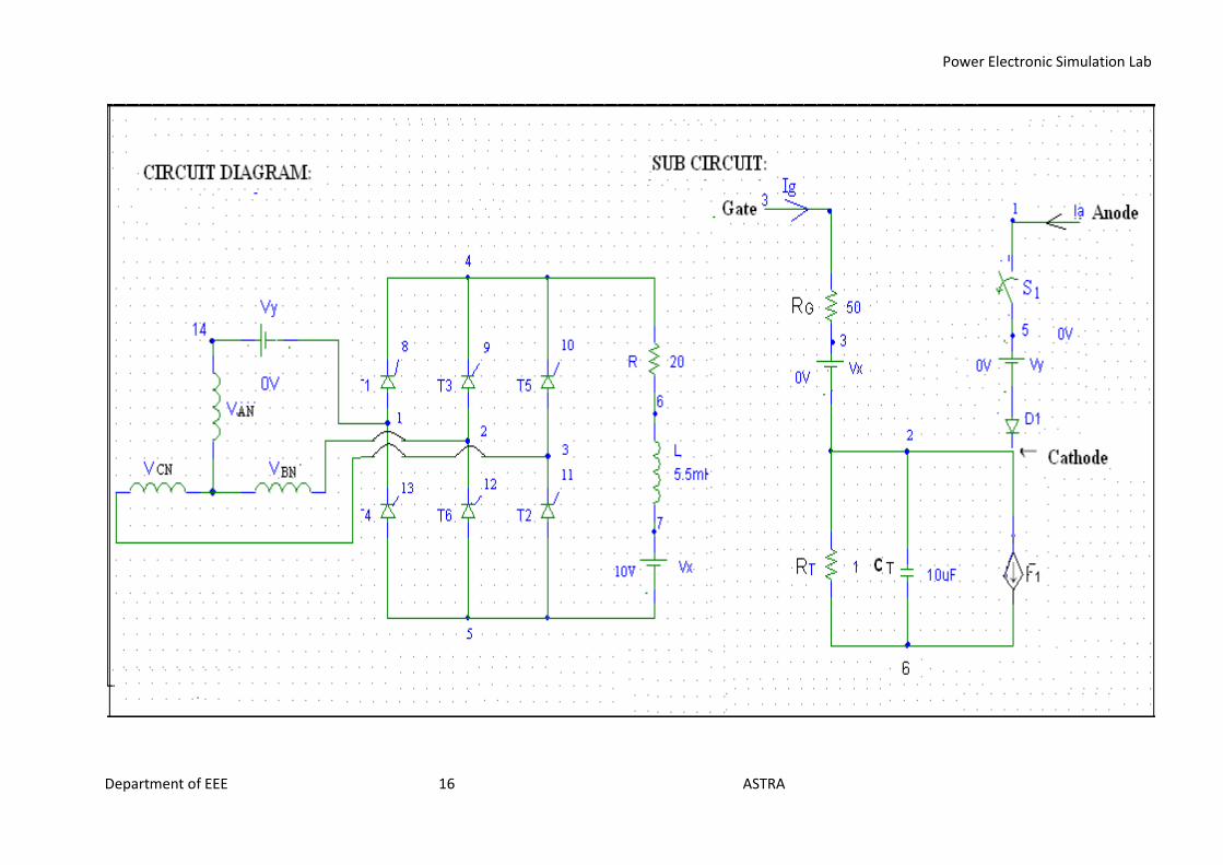
O/p Waveform Details:
V(4,5) ------ Voltage across the load terminals.
I(Vx) ------- Current through the load.
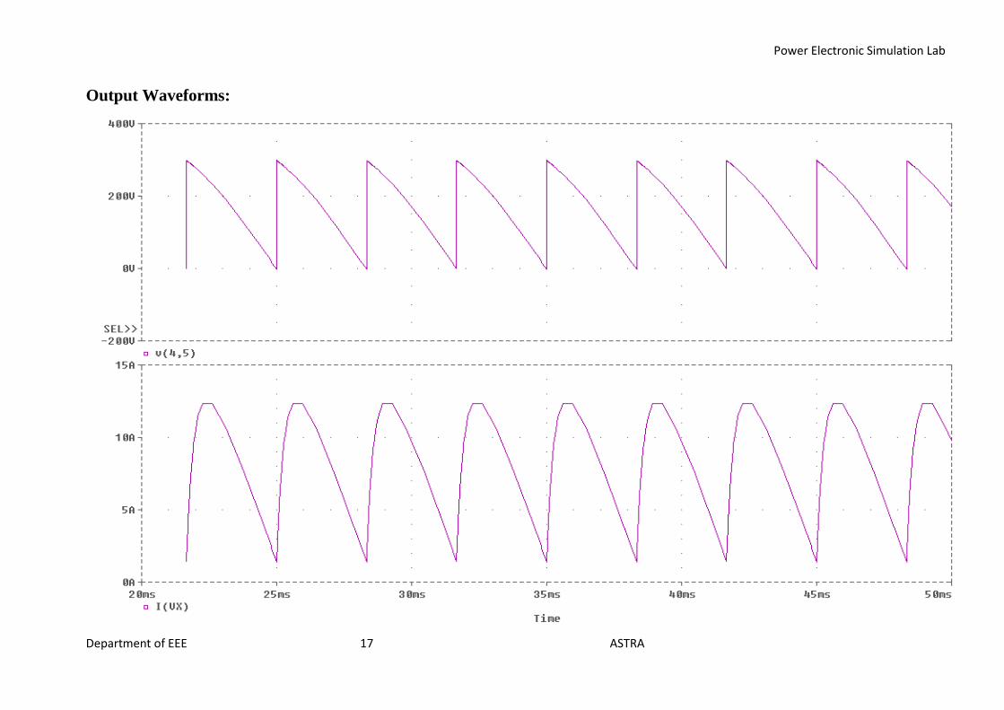
V(14,0)------ Voltage across the Van to Neutral.
V(2,0) ------ Voltage across the Vbn to Neutral.
V(3,0) ------ Voltage across the Vcn to Neutral.
V(1,8) ------ Voltage across the T1.
V(2,9) ------ Voltage across the T2.
V(3,10) ------ Voltage across the T3.
Result: Analysis of three phase full controlled converter circuit has been
Successfully completed.
Power Electronic Simulation Lab
Department of EEE 16 ASTRA
Power Electronic Simulation Lab
Department of EEE 17 ASTRA
Output Waveforms:
Power Electronic Simulation Lab
Department of EEE 18 ASTRA
Output Waveforms:

Power Electronic Simulation Lab
Department of EEE 19 ASTRA
Output Waveforms:

Power Electronic Simulation Lab
Department of EEE 20 ASTRA
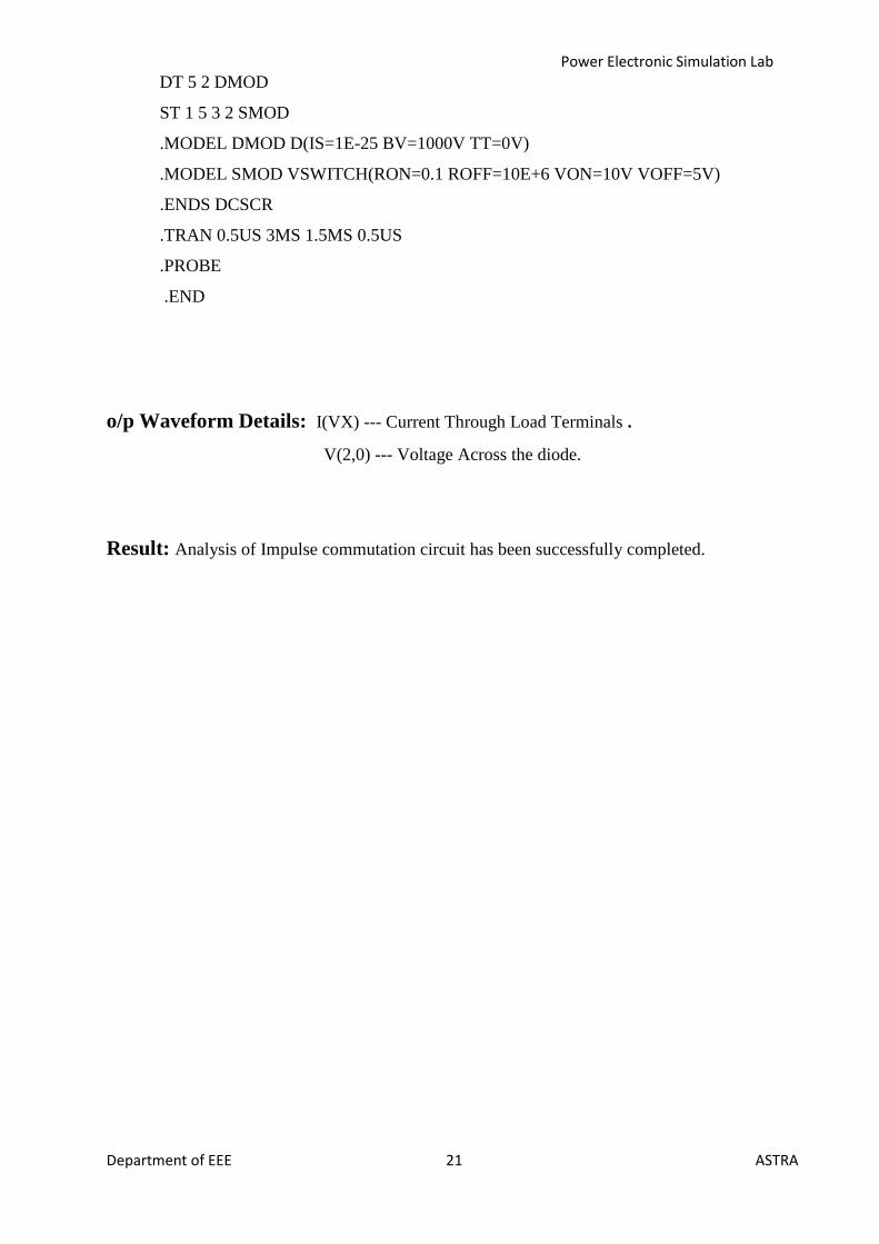
6.4 IMPULSE COMMUTATION CIRCUIT
EXP NO:
Date:
Aim: To simulation Impulse Commutation Circuit by using PSPICE.
Software Required: PSPICE (Personal Computer Simulated Program with
Integrated Circuit Emphasis.
Program:
VS 1 0 DC 200V
VG1 5 0 PULSE(0V 100V 0 1US 0 0.4MS 1MS)
VG2 6 0 PULSE(0V 100V 0.4S 1US 1US 0.6MS 1MS)
VG3 7 0 PULSE(0V 100V 0 1US 1US 0.2MS 1MS)
RG1 5 0 10MEG
RG2 6 0 10MEG
RG3 7 0 10MEG
C 12 9 20UF IC=200V
LR 1 10 5UH
L1 1 13 25UH
D1 2 13 DMOD
DM 2 0 DMOD
.MODEL DMOD D(IS=1E-25 BV=1000V TT=0)
RM 2 3 10
LM 3 4 20MH
VX 4 0 DC 0V
VY 1 8 DC 0V
VZ 10 11 DC 0V
VA 8 12 DC 0V
XT1 8 2 5 0 DCSCR
XT2 11 9 6 0 DCSCR
XT3 9 2 7 0 DCSCR
.SUBCKT DCSCR 1 2 3 4
Power Electronic Simulation Lab
Department of EEE 21 ASTRA
DT 5 2 DMOD
ST 1 5 3 2 SMOD
.MODEL DMOD D(IS=1E-25 BV=1000V TT=0V)
.MODEL SMOD VSWITCH(RON=0.1 ROFF=10E+6 VON=10V VOFF=5V)
.ENDS DCSCR
.TRAN 0.5US 3MS 1.5MS 0.5US
.PROBE
.END
o/p Waveform Details: I(VX) --- Current Through Load Terminals .
V(2,0) --- Voltage Across the diode.
Result: Analysis of Impulse commutation circuit has been successfully completed.

Power Electronic Simulation Lab
Department of EEE 22 ASTRA
Power Electronic Simulation Lab
Department of EEE 23 ASTRA
Output Waveforms:

Power Electronic Simulation Lab
Department of EEE 24 ASTRA
6.5 THREE PHASE INVERTER WITH PWM
CONTROLLER
EXP NO:
Date:
Aim: To simulation three phase Inverter with PWM controller circuit by using PSPICE.
Software Required: PSPICE (Personal Computer Simulated Program with
Integrated Circuit Emphasis.
Program:
VS 1 0 DC 100V
RB1 22 6 50
VG1 22 3 PULSE(0 40V 0 1NS 1NS 0.5MS 1MS)
RB2 16 15 50
VG2 16 0 PULSE(0 40V 166.67US 1NS 1NS 0.5MS 1MS)
RB3 8 7 50
VG3 8 4 PULSE(0 40V 333.33US 1NS 1NS 0.5MS 1MS)
RB4 12 11 50
VG4 12 0 PULSE(0 40V 550US 1NS 1NS 0.5MS 1MS)
RB5 10 9 50
VG5 10 5 PULSE(0 40V 666.67US 1NS 1NS 0.5MS 1MS)
RB6 14 13 50
VG6 14 0 PULSE(0 40V 833.33US 1NS 1NS 0.5MS 1MS)
VY 1 2 DC 0V
VX 3 20 DC 0V
RA 20 17 10
LA 17 21 5MH
RB 4 18 10
LB 18 21 5MH
RC 5 19 10
LC 19 21 5MH
D1 3 2 DMOD
D3 4 2 DMOD
D5 5 2 DMOD
D2 0 5 DMOD
D4 0 3 DMOD
D6 0 4 DMOD
.MODEL DMOD D(IS=2.2E-15 BV=1200V TT=0)
Power Electronic Simulation Lab
Department of EEE 25 ASTRA
Q1 2 6 3 3 2N6546
Q3 2 7 4 4 2N6546
Q5 2 9 5 5 2N6546
Q2 5 15 0 0 2N6546
Q4 3 11 0 0 2N6546
Q6 4 13 0 0 2N6546
.MODEL 2N6546 NPN(IS=2.33E-27 BF=13 CJE=1PF CJC=607.3PF TF=26.5NS)
.TRAN 5US 2.5MS 1.0MS
.PROBE
.OPTIONS ABSTOL=1.0U RELTOL=1.0M VNTOL=1 ITL5=20000
.FOUR 1KHZ I(VX) V(3,21)
.END
O/p Waveform Details: V(5,3) – Voltage across the R,B phases.
V(4,5) – Voltage across the Y,B phases.
V(3,4) – Voltage across the R,Y phases.
Result: Analysis of three phase inverter with PWM controller circuit has been
Successfully completed.

Power Electronic Simulation Lab
Department of EEE 26 ASTRA
CIRCUIT DIAGRAM:

Power Electronic Simulation Lab
Department of EEE 27 ASTRA
Output Waveforms:

Power Electronic Simulation Lab
Department of EEE 28 ASTRA
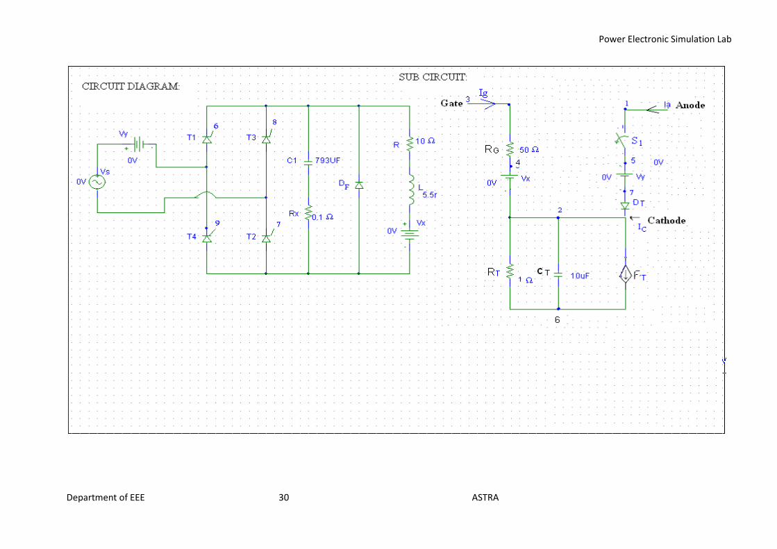
6.6 SINGLE PHASE FULL CONVERTER USING RL &
E LOADS
EXP NO:
Date:
Aim: To analyze the simulation of 1Ø full controlled converter with RL & E load.
Software Required: PSPICE (Personal Computer Simulated Program with
Integrated Circuit Emphasis.
Program:
VS 10 0 SIN(0 169.7V 60HZ)
VG1 6 2 PULSE(0V 10V 2777.78US 1NS 1NS 100US 16666.7US)
VG2 7 0 PULSE(0V 10V 2777.78US 1NS 1NS 100US 16666.7US)
VG3 8 0 PULSE(0V 10V 11111.1US 1NS 1NS 100US 16666.7US)
VG4 9 1 PULSE(0V 10V 11111.1US 1NS 1NS 100US 16666.7US)
*DF 3 2 DMOD
R1 2 4 10
L1 4 5 20MH
C1 2 11 793UF
RX 11 3 0.1
VX 5 3 DC 10V
VY 10 1 DC 0V
XT1 1 2 6 2 SCR
XT2 3 0 7 0 SCR
XT3 0 2 8 2 SCR
XT4 3 1 9 1 SCR
.SUBCKT SCR 1 2 3 2
S1 1 5 6 2 SMOD
RG 3 4 50
VX 4 2 DC 0V
VY 5 7 DC 0V
DT 7 2 DMOD
Power Electronic Simulation Lab
Department of EEE 29 ASTRA
RT 2 6 1
CT 6 2 10UF
F1 2 6 POLY(2) VX VY 0 50 11
.MODEL SMOD VSWITCH( RON=0.0125 ROFF=10E+5 VON=5V VOFF=0V )
.MODEL DMOD D( IS=2.2E-15 BV=1800 TT=0)
.ENDS SCR
.TRAN 10US 100MS 16.6MS
.PROBE
.FOUR 120HZ I(VX)
.END
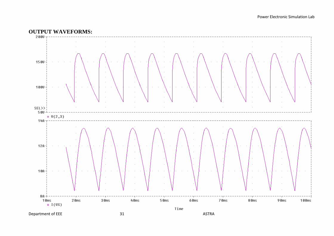
O/p Waveform Details: V(2,3) – Voltage across the load terminals.
I(Vx) – current across the load terminals.
Result: Analysis of 1Ø full controlled converter circuit has been successfully completed.
Power Electronic Simulation Lab
Department of EEE 30 ASTRA
Power Electronic Simulation Lab
Department of EEE 31 ASTRA
OUTPUT WAVEFORMS:
Power Electronic Simulation Lab
Department of EEE 32 ASTRA
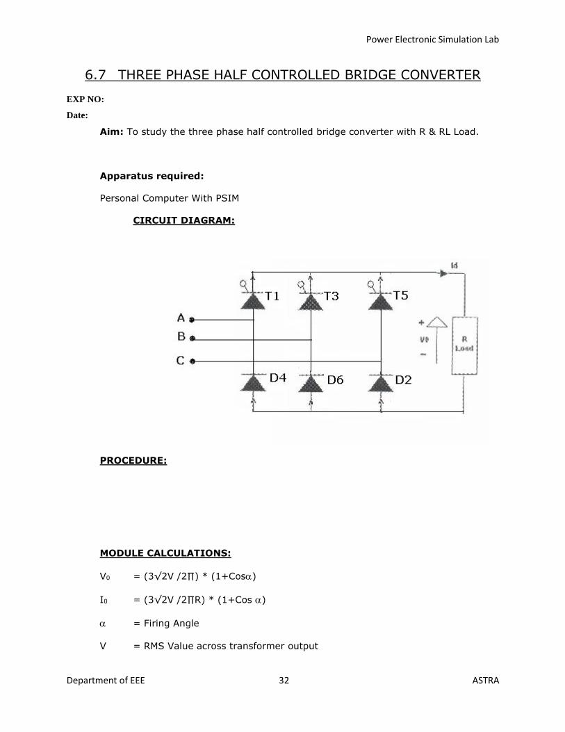
6.7 THREE PHASE HALF CONTROLLED BRIDGE CONVERTER
EXP NO:
Date:
Aim: To study the three phase half controlled bridge converter with R & RL Load.
Apparatus required:
Personal Computer With PSIM
CIRCUIT DIAGRAM:
PROCEDURE:
MODULE CALCULATIONS:
V0 = (3√2V /2∏) * (1+Cos)
I0 = (3√2V /2∏R) * (1+Cos )
= Firing Angle
V = RMS Value across transformer output

Power Electronic Simulation Lab
Department of EEE 33 ASTRA
MODEL GRAPH:
RESULT: The three phase half controlled bridge converter with R & RL Load is
studied.
Power Electronic Simulation Lab
Department of EEE 34 ASTRA
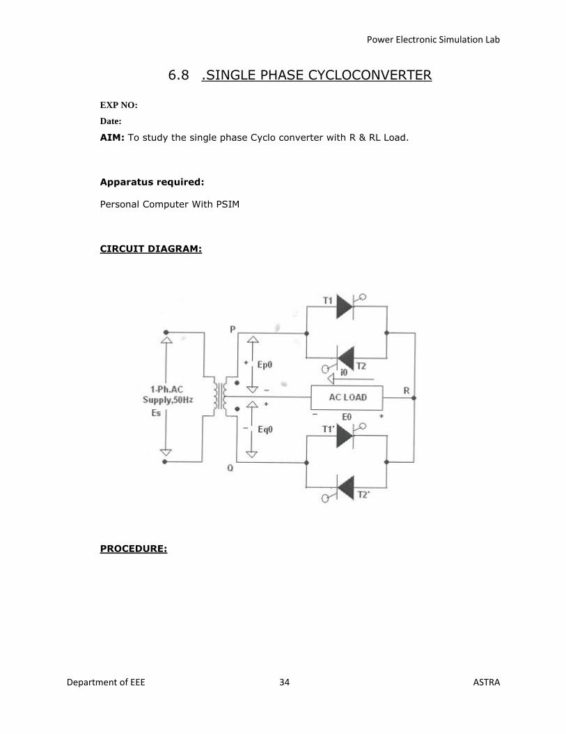
6.8 .SINGLE PHASE CYCLOCONVERTER
EXP NO:
Date:
AIM: To study the single phase Cyclo converter with R & RL Load.
Apparatus required:
Personal Computer With PSIM
CIRCUIT DIAGRAM:
PROCEDURE:
Power Electronic Simulation Lab
Department of EEE 35 ASTRA
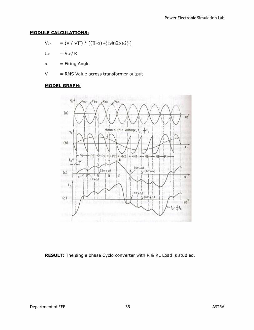
MODULE CALCULATIONS:
V0r = (V / √∏) * [(∏-sin2
I0r = V0r / R
= Firing Angle
V = RMS Value across transformer output
MODEL GRAPH:
RESULT: The single phase Cyclo converter with R & RL Load is studied.
Power Electronic Simulation Lab
Department of EEE 36 ASTRA
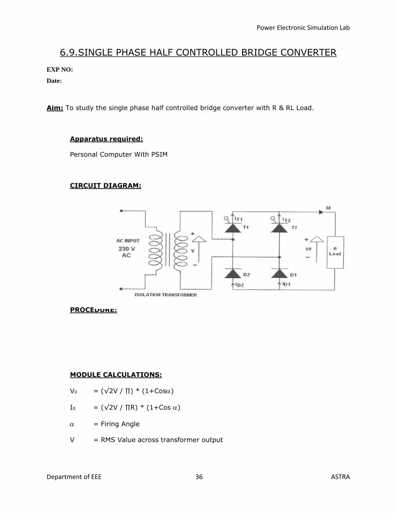
6.9.SINGLE PHASE HALF CONTROLLED BRIDGE CONVERTER
EXP NO:
Date:
Aim: To study the single phase half controlled bridge converter with R & RL Load.
Apparatus required:
Personal Computer With PSIM
CIRCUIT DIAGRAM:
PROCEDURE:
MODULE CALCULATIONS:
V0 = (√2V / ∏) * (1+Cos)
I0 = (√2V / ∏R) * (1+Cos )
= Firing Angle
V = RMS Value across transformer output

Power Electronic Simulation Lab
Department of EEE 37 ASTRA
MODEL GRAPH:
RESULT: Hence the single phase half controlled bridge converter with R-Load has
been studied and respective graphs have been plotted after the readings being
tabulated.

Power Electronic Simulation Lab
Department of EEE 38 ASTRA
6.10. SINGLE PHASE FULLY CONTROLLED BRIDGE
CONVERTER
EXP NO:
Date:
Aim: To study the single phase fully controlled bridge converter with R & RL Load.
Apparatus required:
Personal Computer With PSIM
CIRCUIT DIAGRAM:
PROCEDURE:
MODULE CALCULATIONS:
For R-L Load: For R Load:
V0 = (2√2V/∏) * Cos V0 = (√2V/∏) * (1+Cos)
I0 = (2√2V/∏Z) * Cos I0 = (√2V /∏R) * (1+Cos)
= Firing Angle
V = RMS Value across transformer output
Power Electronic Simulation Lab
Department of EEE 39 ASTRA
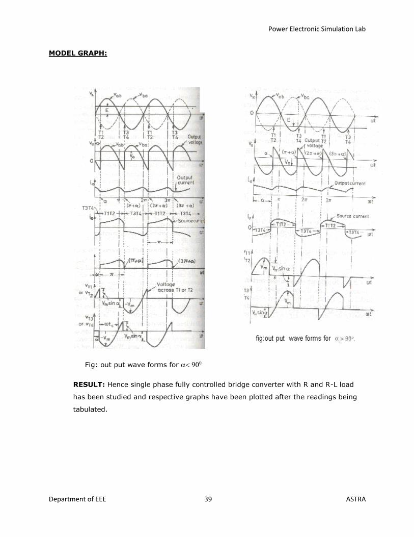
MODEL GRAPH:
Fig: out put wave forms for
RESULT: Hence single phase fully controlled bridge converter with R and R-L load
has been studied and respective graphs have been plotted after the readings being
tabulated.
Power Electronic Simulation Lab
Department of EEE 40 ASTRA
7. Content beyond syllabus:
1. Three phase AC voltage controller
2. Three phase Cyclo converter.
3. Series inverter and Praller inverter
4. Jhones chopper
5. Four quadrent chopper

Power Electronic Simulation Lab
Department of EEE 41 ASTRA

Power Electronic Simulation Lab
Department of EEE 42 ASTRA
Sample Viva Voce Questions
Exp: 6.1.1
1) Explain V-I characteristics of SCR? 2) What are Latching current and Holding current? 3) Define VBO & VBR? Which has a grater value and why? 4) Why is Latching current greater than Holding current? 5) What is the effect of increasing gate current in the turning on of SCR
Exp: 6.2
1) Explain R,RC and UJT triggering? Which is the most effective?
2) What is the maximum possible firing angle in R-Triggering?
3) How the triggering pulses are generated in UJT triggering?
4) How to change the triggering instants in UJT triggering?
5) Explain the waveforms?
Exp: 6.3
1) Explain the working of AC Voltage controller?
2) Define Displacement angle, Displacement factor and distortion factor?
3) Displacement angle * Displacement factor = _______
4) Explain the waveforms with R & RL load?
5) With RL load, the firing angle should be always greater than power factor. Why? (What
is the effect of power factor in the working of an AC voltage controller with RL load?)
Exp: 6.4
1) What are the different configurations for a Fully Controlled converter?
2) Explain the working of a Fully Controlled converter?
3) Explain the waveforms with R & RL loads?
4) What is the equation for average voltage in a Fully Controlled converter?

Power Electronic Simulation Lab
Department of EEE 43 ASTRA
5) What are the applications of a Fully Controlled converter?
Exp: 6.5
1) Explain the working of a Half controlled converter?
2) What are the disadvantages ?
3) Explain the waveforms with R & RL loads?
4) What is the equation for average voltage in a Half controlled converter?
5) What are the two different modes of operation in a Half controlled converter?
Exp: 6.7
1) What are the applications of cycloconverters?
2) How the frequency change is made possible in cycloconverters?
3) What are the different types of cycloconverters? Explain each?
4) Explain the sequence of triggering for (1/3 )rd frequency?
5) Draw & Explain waveforms for RL load?
Exp: 6.8
1) Explain the working of a series inverter?
2) Explain the waveforms?
3) What are the applications?
4) What are the differences between a basic series inverter and a modified one?
Exp: 6.9
1) What is a chopper?
2) What are the different types of Choppers?
3) Explain the working?

Power Electronic Simulation Lab
Department of EEE 44 ASTRA
4) Explain the waveforms?
Exp: 6.10
1 what is other name for class A commutation?
2 what is other name for class B commutation?
3 what is other name for class C commutation?
4 what is other name for class D commutation?
5 what is other name for class E commutation?

Power Electronic Simulation Lab
Department of EEE 45 ASTRA
8. Sample Question paper of the lab external
1 Simulate the Single phase ac voltage controller
2 Simulate the Resonant pulse commutation circuit
3 Simulate the Three phase full converter using rl&e loads
4 Simulate the Impulse commutation circuit
5 Simulate the Three phase inverter with pwm controller
6 Simulate the Single phase full converter
7 Simulate the Three phase half controlled bridge converter
8 Simulate the Single phase cycloconverter
9 Simulate the Single phase half controlled bridge converter
10 Simulate the Single phase fully controlled bridge converter

Power Electronic Simulation Lab
Department of EEE 46 ASTRA
10. Applications of the laboratory :
1 WIth the healp of this lab the student can able to learn the simulation of many power
electronics converters
2 He or she can be able to do the analysis of different pwer electronics devices
3 Can able to learn the performance of many power devices

Power Electronic Simulation Lab
Department of EEE 47 ASTRA
11. Precautions to be taken while conducting the lab
Power must be switched-OFF while making any connections.
Do not come in contact with live supply.
Power should always be in switch-OFF condition, EXCEPT while you are taking readings.
The Circuit diagram should be approved by the faculty before making connections.
Circuit connections should be checked & approved by the faculty before switching on the
power.
Keep your Experimental Set-up neat and tidy.
Check the polarities of meters and supplies while making connections.
Always connect the voltmeter after making all other connections.
Check the Fuse and it’s ratify.
Use right color and gauge of the fuse.
All terminations should be firm and no exposed wire.
Do not use joints for connection wire.
SAFETY – II
1. The voltage employed in electrical lab are sufficiently high to endanger human life.
2. Compulsorily wear shoes.
3. Don’t use metal jewelers on hands.
4. Do not wear loose dress
Don’t switch on main power unless the faculty gives the permission

Power Electronic Simulation Lab
Department of EEE 48 ASTRA
12. Code of Conduct
1 Students should report to the labs concerned as per the timetable.
2. Students who turn up late to the labs will in no case be permitted to perform the
experiment scheduled for the day.
3. After completion of the experiment, certification of the staff in-charge concerned in the
observation book is necessary.
4. Students should bring a notebook of about 100 pages and should enter the
readings/observations/results into the notebook while performing the experiment.
5. The record of observations along with the detailed experimental procedure of the
experiment performed in the immediate previous session should be submitted and
certified by the staff member in-charge.
6. Not more than three students in a group are permitted to perform the experiment on a
set up.
7. The group-wise division made in the beginning should be adhered to, and no mix up of
student among different groups will be permitted later.
8. The components required pertaining to the experiment should be collected from Lab-
in-charge after duly filling in the requisition form.
9. When the experiment is completed, students should disconnect the setup made by
them, and should return all the components/instruments taken for the purpose.
10. Any damage of the equipment or burnout of components will be viewed seriously either
by putting penalty or by dismissing the total group of students from the lab for the
semester/year.
11. Students should be present in the labs for the total scheduled duration.
12. Students are expected to prepare thoroughly to perform the experiment before coming
to Laboratory.
13. Procedure sheets/data sheets provided to the students’ groups should be maintained
neatly and are to be returned after the experiment.

Power Electronic Simulation Lab
Department of EEE 49 ASTRA
13. Graphs if any.