1.1 introduction of materials science and engineering
TRANSCRIPT

2
1.1 Introduction of Materials Science and Engineering
Materials Science – Investigating relationships that exist between the structure and properties of materials.
Materials Engineering – On the basis of these structure-property correlations, designing or engineering the structure of a material to produce a pre-determined set of properties.
Structure
Structure of a material usually relates to the arrangement of its internal components.
Subatomic - Structure involves electrons within the individual atoms and interactions with their nuclei.
Atomic level- structure encompasses the organization of atoms or molecules relative to one another.
Microscopic - Which contains large groups of atoms that are normally agglomerated together.
Macroscopic – viewable with the naked eye.
Property
A property is a material trait in terms of the kind and magnitude of response to a specific imposed stimulus. Properties are made independent of material shape and size.
Example-
A specimen subjected to forces will experience deformation,
A polished metal surface will reflect light.
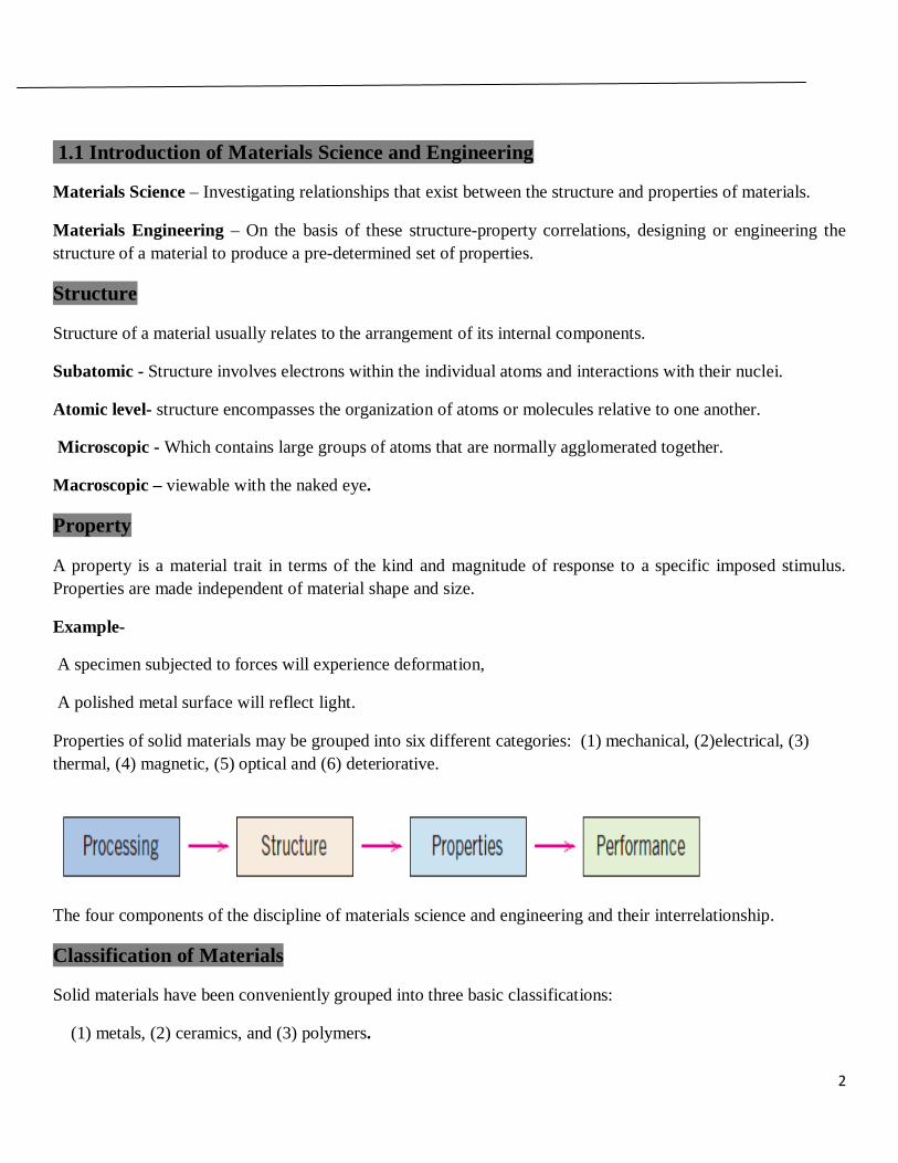
Properties of solid materials may be grouped into six different categories: (1) mechanical, (2)electrical, (3) thermal, (4) magnetic, (5) optical and (6) deteriorative.
The four components of the discipline of materials science and engineering and their interrelationship.
Classification of Materials
Solid materials have been conveniently grouped into three basic classifications:
(1) metals, (2) ceramics, and (3) polymers.

3
1. Metals-
• Materials in this group are composed of one or more metallic elements (such as iron, aluminum, copper, titanium, gold, and nickel), and often also nonmetallic elements (for example, carbon, nitrogen, and oxygen) in relatively small amounts.
• Atoms in metals and their alloys are arranged in a very orderly manner. • In comparison to the ceramics and polymers, are relatively dense. • Mechanical Property- relatively stiff and strong , ductile (i.e., capable of large amounts of deformation
without fracture), and are resistant to fracture. • Metallic materials have large numbers of nonlocalized electrons; that is, these electrons are not bound to
particular atoms.Many properties of metals are directly attributable to these electrons. • Example, metals are extremely good conductors of electricity,and heat, and are not transparent to visible
light; a polished metal surface has a lustrous appearance. • Some of the metals (viz., Fe, Co, and Ni) have desirable magnetic properties.
2. Ceramics
• Ceramics are compounds between metallic and nonmetallic elements; they are most frequently oxides, nitrides, and carbides.
• Examples-aluminum oxide (or alumina, Al2O3), silicon dioxide (or silica, SiO2),silicon carbide (SiC), silicon nitride (Si3N4).
• Examples of traditional ceramics — clay minerals (i.e., porcelain), cement, and glass.
Properties-
• Relatively stiff and strong—stiffnesses and strengths are comparable to those of the metals , very hard, extremely brittle (lack ductility),.highly susceptible to fracture.
• Thermal and electrical Properties- Insulative to the passage of heat and electricity low electrical conductivities and are more resistant to high temperatures
• Optical characteristics-Ceramics may be transparent, translucent, or opaque.
Polymers
Carbon-based compounds
• Chain of H-C molecules. Each repeat unit of H-C is a monomer e.g. ethylene (C2H4), Polyethylene – (–CH2 –CH2)n.
• Polymers include the familiar plastic and rubber materials. • Many of them are organic compounds that are chemically based on carbon, hydrogen, and other
nonmetallic elements (viz. O, N, and Si). • They have very large molecular structures, often chain-like in nature that have a backbone of carbon
atoms. Some of the common and familiar polymers are polyethylene (PE), nylon, poly (vinyl chloride)(PVC), polycarbonate (PC), polystyrene (PS), and silicone rubber.
4
Properties
• Low densities, not as stiff nor as strong as ceramics and metals. • Extremely ductile and pliable (i.e., plastic). • Relatively inert chemically and unreactive in a large number of environments.
Limitations
• Tendency to soften and/or decompose at modest temperatures, which, in some instances,limits their use. • Low electrical conductivities and are nonmagnetic.
Composites
• A composite is composed of two (or more) individual materials, which come from the categories discussed above—viz., metals, ceramics, and polymers.
• Objective-to achieve a combination of properties that is not displayed by any single material
Examples
• Cemented carbides (WC with Co binder) • Plastic molding compounds containing fillers • Rubber mixed with carbon black • Wood (a natural composite as distinguished from a synthesized composite)
Advance Materials
• Materials that are utilized in high-technology (or high-tech) applications are sometimes termed advanced materials.
Examples
• Include electronic equipment (camcorders, CD/DVD players, etc.), computers, fiber-optic systems, spacecraft, aircraft, and military rocketry, liquid crystal displays (LCDs), and fiber optics.
• These advanced materials may be typically traditional materials types (e.g., metals, ceramics, polymers) whose properties have been enhanced, and, also newly developed, high-performance materials.
• Advanced materials include semiconductors, biomaterials, and what we may term“ materials of the future.
Biomaterials
• Biomaterials are employed in components implanted into the human body for replacement of diseased or damaged body parts.
• These materials must not produce toxic substances and must be compatible with body tissues (i.e., must not cause adverse biological reactions).
• All of the above materials—metals, ceramics, polymers, composites, and semiconductors—may be used as biomaterials.

5
Example-
Titanium and its alloy, Co-Cr alloy, stainless steel, zirconia, HA, TiO2 etc.
Semiconductors
• Semiconductors have electrical properties that are intermediate between the electrical conductors (viz. metals and metal alloys) and insulators (viz. ceramics and polymers).
• The electrical characteristics of these materials are extremely sensitive to the presence of minute concentrations of impurity atoms, for which the concentrations may be controlled over very small spatial regions.
• Semiconductors have made possible the advent of integrated circuitry that has totally revolutionized the electronics and computer industries (not to mention our lives) over the past three decades.
The Materials Selection Process
• Pick Application and determine required Properties. • Properties: mechanical, electrical, thermal, magnetic, optical, deteriorative. • Properties- Identify candidate Material(s) • Material: structure, composition. • Material- Identify required Processing • Processing: changes structure and overall shape
Example: casting, sintering, vapor deposition, doping forming, joining, annealing.
1.2 Defects in Solids
• The term “defect” or “imperfection” is generally used to describe any deviation from the perfect periodic array of atoms in the crystal.
• The properties of some materials are extremely influenced by the presence of imperfections such as mechanical strength, ductility, crystal growth, magnetic hysteresis, dielectric strength, condition in semiconductors, which are termed structure sensitive are greatly affected by the-relatively minor changes in crystal structure caused by defects or imperfections.
• There are some properties of materials such as stiffness, density and electrical conductivity which are termed structure-insensitive, are not affected by the presence of defects in crystals.
• It is important to have knowledge about the types of imperfections that exist and the roles they play in affecting the behavior of materials.
• Crystal imperfections can be classified on the basis of their geometry as

6
Point Defects in Metals
It is a zero dimension defect, associated with one or two atomic positions.
Vacancies -The simplest of the point defects is a vacancy, or vacant lattice site, one normally occupied from which an atom is missing. All crystalline solids contain vacancies and, in fact, it is not possible to create such a material that is free of these defects, vacant atomic sites in a structure.
Self-Interstitials- when an atom occupies an interstitial site where no atom would ordinarily appear, causing an interstitialcy.
7
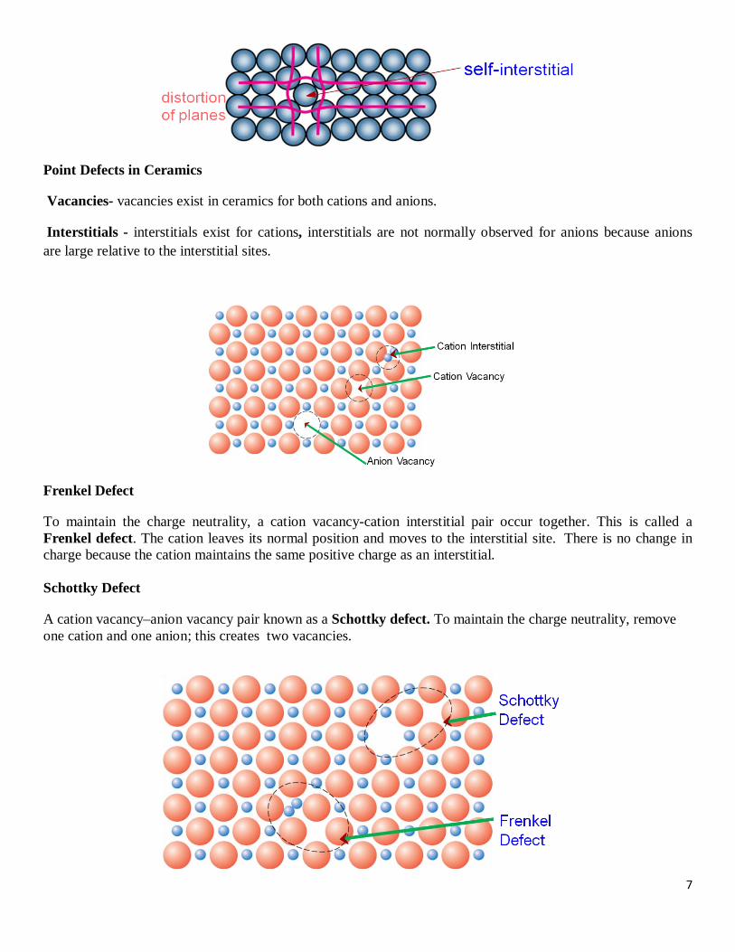
Point Defects in Ceramics
Vacancies- vacancies exist in ceramics for both cations and anions.
Interstitials - interstitials exist for cations, interstitials are not normally observed for anions because anions are large relative to the interstitial sites.
Frenkel Defect
To maintain the charge neutrality, a cation vacancy-cation interstitial pair occur together. This is called a Frenkel defect. The cation leaves its normal position and moves to the interstitial site. There is no change in charge because the cation maintains the same positive charge as an interstitial. Schottky Defect
A cation vacancy–anion vacancy pair known as a Schottky defect. To maintain the charge neutrality, remove one cation and one anion; this creates two vacancies.

8
The equilibrium number of vacancies for a given quantity of material depends on and increases with temperature according to
Equilibrium concentration varies with temperature
Where, N is the total number of atomic sites, Qv is the energy required for the formation of a vacancy, T is the absolute temperature in kelvins, and k is the gas or Boltzmann’s constant. 1.38 x 10⁻²³ J/atom-K. Equilibrium Concentration:
1. Find the equilibrium concentration of vacancies in aluminium and nickel at 0K,300 K and 900K. Given ∆Hf= 68 ×103 KJ/mol.
Solution-
(i) at 0K
(ii) at 300 K
2. Calculate the equilibrium number of vacancies per cubic meter for copper at 1000oC. The energy for vacancy formation is 0.9 eV/atom; the atomic weight and density (at 1000oC) for copper are 63.5 g/mol and 8.4 g/cm3, respectively. Solution- The value of N, the number of atomic sites per cubic meter for copper, from its atomic weight its density and Avogadro’s number according to

9
=8.0 1028 atoms/m3
Thus, the number of vacancies at 1000oC (1273K) is equal to
= 2.2 ×1025 vacancies/m3
EFFECT OF POINT IMPERFECTIONS
• The presence of a point imperfection introduces distortions in the crystal. • In the case of impurity atom, because of its difference in size, elastic strains are created in the
regions surrounding the impurity atom. • All these factors tend to increase the potential energy of the crystal called ‘enthalpy’. The work done
for the creation of such a point defect is called the ‘enthalpy of formation’ of the point imperfection
LINE IMPERFECTIONS
• A dislocation is a linear or one-dimensional defect around which some of the atoms are misaligned. The defects, which take place due to distortion of atoms along a line, in some direction are called as ‘line defects,.Line defects are also called dislocations.
• It is responsible for the phenomenon of slip by which most metals deform plastically.
The two types of dislocations are,
Edge dislocation
• It is a linear defect that centers around the line that is defined along the end of the extra half-plane of atoms.
• The distorted configuration extends all along the edge into the crystal. • Thus as the region of maximum distortion is centered around the edge of the incomplete plane, this
distortion represents a line imperfection and is called an edge dislocation. • Edge dislocations are represented by ‘⊥’ or ‘Τ‘ depending on whether the incomplete plane starts from
the top or from the bottom of the crystal. • These two configurations are referred to as positive and negative edge dislocations respectively.

10
Screw dislocation:-
• In this dislocation, the atoms are displaced in two separate planes perpendicular to each other.
• It forms a spiral ramp around the dislocation.
• The Burgers Vector is parallel to the screw dislocation line.
• Speed of movement of a screw dislocation is lesser compared to edge dislocation.
Burgers vector - The magnitude and direction of the lattice distortion associated with a dislocation is expressed in terms of a Burgers vector, denoted by a b. The Burger vector can be found by the gap in the Burger circuit which is obtained by moving equal distances in each direction around the dislocation.

11
Mixed dislocations - Most dislocations found in crystalline materials are probably neither pure edge nor pure screw, but exhibit components of both types; these are termed mixed dislocations. Surface imperfections
• Surface imperfections arise from a change in the stacking of atomic planes on or across a boundary. • The change may be one of the orientations or of the stacking sequence of atomic planes. • In geometric concept, surface imperfections are two- dimensional. They are of two types external and
internal surface imperfections. External Surfaces
• They are the imperfections represented by a boundary. At the boundary the atomic bonds are terminated. • Surface atoms are not bonded to the maximum number of nearest neighbors, and are therefore in a
higher energy state than the atoms at interior positions. The bonds of these surface atoms that are not satisfied give rise to a surface energy, expressed in units of energy per unit area (J/m2 or erg/cm2).
Grain Boundaries • The boundary separating two small grains or crystals having different crystallographic orientations in
polycrystalline materials.

12
Twin Boundaries
• A twin boundary is a special type of grain boundary across which there is a specific mirror lattice symmetry; that is, atoms on one side of the boundary are located in mirror-image positions of the atoms on the other side.
• The region of material between these boundaries is appropriately termed a twin. • Twins result from atomic displacements that are produced from applied mechanical shear forces
(mechanical twins), and also during annealing heat treatments following deformation (annealing twins). Volume Defects- These include pores, cracks, foreign inclusions, and other phases. They are normally introduced during processing and fabrication steps. Effect on property
• There are some properties of materials such as stiffness, density and electrical conductivity which are termed structure-insensitive, are not affected by the presence of defects in crystals while there are many properties of greatest technical importance such as mechanical strength, ductility, crystal growth, magnetic.
• Hysteresis, dielectric strength, condition in semiconductors, which are termed structure sensitive are
greatly affected by the-relatively minor changes in crystal structure caused by defects or imperfections.
1.3 Diffusion in solids
Diffusion is a process of mass transport by atomic movement under the influence of thermal energy and a concentration gradient. Atoms move from higher to lower concentration region.

13
Figure 1. (a) A copper–nickel diffusion couple after a high-temperature heat treatment, showing the alloyed diffusion zone. (b) Schematic representations of Cu (red circles) and Ni (blue circles) atom locations within the couple. (c) Concentrations of copper and nickel as a function of position across the couple. Figure 1 shows, pure copper and nickel at the two extremities of the couple, separated by an alloyed region. Concentrations of both metals vary with position as shown in Figure1(c). This result indicates that copper atoms have migrated or diffused into the nickel, and that nickel has diffused into copper. Diffusion Mechanisms Diffusion is just the stepwise migration of atoms from lattice site to lattice site. In fact, the atoms in solid materials are in constant motion. For an atom to make such a move, two conditions must be met: (1) there must be an empty adjacent site, and (2) the atom must have sufficient energy to break bonds with its neighbor atoms and then cause some lattice distortion during the displacement. Vacancy Diffusion In this mechanism involves the interchange of an atom from a normal lattice position to an adjacent vacant lattice site or vacancy. This process necessitates the presence of vacancies, and the extent to which vacancy diffusion can occur is a function of the number of these defects that are present. Diffusing atoms and vacancies exchange positions, the diffusion of atoms in one direction corresponds to the motion of vacancies in the opposite direction. Both self-diffusion and inter-diffusion occur by this mechanism.

14
Interstitial Diffusion In this diffusion involves atoms that migrate from an interstitial position to a neighboring one that is empty. This mechanism is found for inter-diffusion of impurities such as hydrogen, carbon, nitrogen, and oxygen, which have atoms that are small enough to fit into the interstitial positions. In most metal alloys, interstitial diffusion occurs much more rapidly than diffusion by the vacancy mode, since the interstitial atoms are smaller and thus more mobile.
15
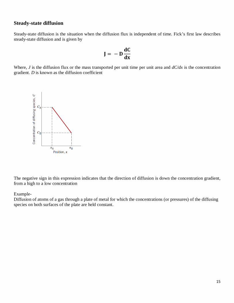
Steady-state diffusion Steady-state diffusion is the situation when the diffusion flux is independent of time. Fick’s first law describes steady-state diffusion and is given by
Where, J is the diffusion flux or the mass transported per unit time per unit area and dC/dx is the concentration gradient. D is known as the diffusion coefficient The negative sign in this expression indicates that the direction of diffusion is down the concentration gradient, from a high to a low concentration Example- Diffusion of atoms of a gas through a plate of metal for which the concentrations (or pressures) of the diffusing species on both surfaces of the plate are held constant.

GATE Study Material MaterialsEngineering And Metallurgy(Production And Industrial
Engineering)
Publisher : Faculty Notes Author : Panel Of Experts
Type the URL : http://www.kopykitab.com/product/10083
Get this eBook
84%OFF