12-bitoctal-channeladc family up to 65msps · 12-bit adc pll serializer 1x adclk 6x adclk in1 p in1...
TRANSCRIPT
12-BitADC
PLL
Serializer
1x ADCLK
6x ADCLK
IN1P
IN1N
OUT1P
OUT1N
LCLKP
LCLKN
ADCLKP
ADCLKN
12x ADCLK
12-BitADC
Serializer
Digital
Digital
Reference
IN8P
IN8N
RE
FT
INT
EX
T
RE
FB
VC
M
OUT8P
OUT8N
I SE
T
Registers
SD
ATA
CS
RE
SE
T
SC
LK
ADC
Control
PD
Clock
Buffer
(AD
CLK
)
CLK
P
(AV
SS
)
CLK
N
AV
DD
(33
V)
LV
DD
(18
V)
Power-
Down
Test P
attern
s
Drive C
urr
ent
Outp
ut F
orm
at
Dig
ital G
ain
(0dB
to 1
2dB
)
frac14 frac14 frac14 frac14frac14 frac14
Channels
2 to 7
ADS5281ADS5282
wwwticom SBAS397I ndashDECEMBER 2006ndashREVISED JUNE 2012
12-Bit Octal-Channel ADC Family Up to 65MSPSCheck for Samples ADS5281 ADS5282
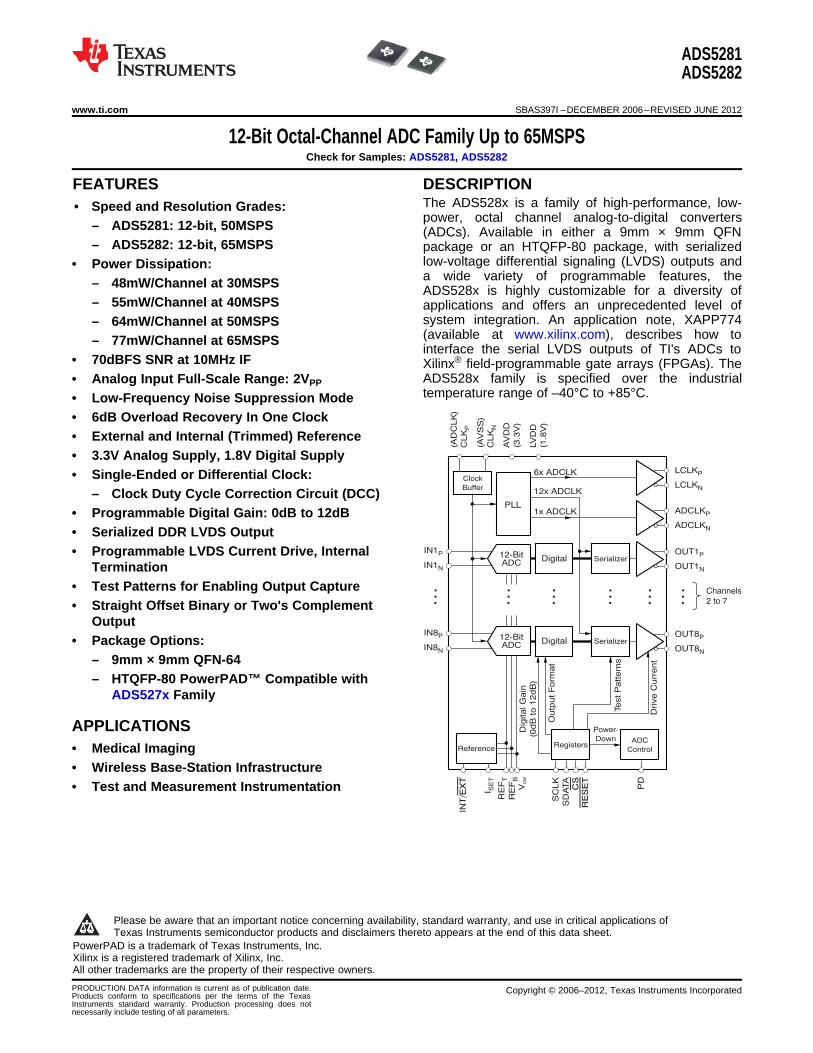
1FEATURES DESCRIPTIONThe ADS528x is a family of high-performance low-
234bull Speed and Resolution Gradespower octal channel analog-to-digital converters
ndash ADS5281 12-bit 50MSPS (ADCs) Available in either a 9mm times 9mm QFNndash ADS5282 12-bit 65MSPS package or an HTQFP-80 package with serialized
low-voltage differential signaling (LVDS) outputs andbull Power Dissipationa wide variety of programmable features thendash 48mWChannel at 30MSPS ADS528x is highly customizable for a diversity of
ndash 55mWChannel at 40MSPS applications and offers an unprecedented level ofsystem integration An application note XAPP774ndash 64mWChannel at 50MSPS(available at wwwxilinxcom) describes how tondash 77mWChannel at 65MSPSinterface the serial LVDS outputs of TIs ADCs to
bull 70dBFS SNR at 10MHz IF Xilinxreg field-programmable gate arrays (FPGAs) TheADS528x family is specified over the industrialbull Analog Input Full-Scale Range 2VPPtemperature range of ndash40degC to +85degCbull Low-Frequency Noise Suppression Mode
bull 6dB Overload Recovery In One Clockbull External and Internal (Trimmed) Referencebull 33V Analog Supply 18V Digital Supplybull Single-Ended or Differential Clock
ndash Clock Duty Cycle Correction Circuit (DCC)bull Programmable Digital Gain 0dB to 12dBbull Serialized DDR LVDS Outputbull Programmable LVDS Current Drive Internal
Terminationbull Test Patterns for Enabling Output Capturebull Straight Offset Binary or Twos Complement
Outputbull Package Options
ndash 9mm times 9mm QFN-64ndash HTQFP-80 PowerPADtrade Compatible with
ADS527x Family
APPLICATIONSbull Medical Imagingbull Wireless Base-Station Infrastructurebull Test and Measurement Instrumentation
1
Please be aware that an important notice concerning availability standard warranty and use in critical applications ofTexas Instruments semiconductor products and disclaimers thereto appears at the end of this data sheet
2PowerPAD is a trademark of Texas Instruments Inc3Xilinx is a registered trademark of Xilinx Inc4All other trademarks are the property of their respective owners
PRODUCTION DATA information is current as of publication date Copyright copy 2006ndash2012 Texas Instruments IncorporatedProducts conform to specifications per the terms of the TexasInstruments standard warranty Production processing does notnecessarily include testing of all parameters
ADS5281ADS5282
SBAS397I ndashDECEMBER 2006ndashREVISED JUNE 2012 wwwticom
This integrated circuit can be damaged by ESD Texas Instruments recommends that all integrated circuits be handled withappropriate precautions Failure to observe proper handling and installation procedures can cause damage
ESD damage can range from subtle performance degradation to complete device failure Precision integrated circuits may be moresusceptible to damage because very small parametric changes could cause the device not to meet its published specifications
RELATED PRODUCTSMODEL RESOLUTION (BITS) SAMPLE RATE (MSPS) CHANNELS
ADS5281 12 50 8
ADS5282 12 65 8
ADS5287 10 65 8
ADS5270 12 40 8
ADS5271 12 50 8
ADS5272 12 65 8
ADS5273 12 70 8
ADS5242 12 65 4
Table 1 ORDERING INFORMATION (1) (2)
SPECIFIEDPACKAGE TEMPERATURE PACKAGE ORDERING TRANSPORT
PRODUCT PACKAGE-LEAD DESIGNATOR RANGE MARKING NUMBER MEDIA QUANTITY (3)
ADS5281IPFP TrayHTQFP-80 PFP ADS5281I(PowerPAD) ADS5281PFPR Tape and ReelADS5281 ndash40degC to +85degC
ADS5281IRGCT Tape and ReelQFN-64 RGC AZ5281
ADS5281IRGCR Tape and Reel
ADS5282IRGCT Tape and ReelADS5282 QFN-64 RGC ndash40degC to +85degC AZ5282
ADS5282IRGCR Tape and Reel
(1) For the most current package and ordering information see the Package Option Addendum at the end of this document or see the TIweb site at wwwticom
(2) These devices meet the following planned eco-friendly classificationGreen (RoHS and No SbBr) Texas Instruments defines Green to mean Pb-free (RoHS compatible) and free of bromine (Br)- andantimony (Sb)-based flame retardants Refer to the Quality and Lead-Free (Pb-Free) Data web site for more information These deviceshave a Cu NiPdAu leadball finish
(3) Refer to the Package Option Addendum at the end of this document for specific transport media and quantity information
ABSOLUTE MAXIMUM RATINGS (1)
Over operating free-air temperature range unless otherwise noted
ADS528x UNIT
Supply voltage range AVDD ndash03 to +39 V
Supply voltage range LVDD ndash03 to +22 V
Voltage between AVSS and LVSS ndash03 to +03 V
External voltage applied to REFT pin ndash03 to +3 V
External voltage applied to REFB pin ndash03 to +2 V
Voltage applied to analog input pins ndash03 to minimum [36 (AVDD + 03)] V
Voltage applied to digital input pins ndash03 to minimum [39 (AVDD + 03)] V
Peak solder temperature +260 degC
Junction temperature +125 degC
Storage temperature range ndash65 to +150 degC
(1) Stresses above these ratings may cause permanent damage Exposure to absolute maximum conditions for extended periods maydegrade device reliability These are stress ratings only and functional operation of the device at these or any other conditions beyondthose specified is not supported
2 Copyright copy 2006ndash2012 Texas Instruments Incorporated
ADS5281ADS5282
wwwticom SBAS397I ndashDECEMBER 2006ndashREVISED JUNE 2012
RECOMMENDED OPERATING CONDITIONS (1)
ADS528x
PARAMETER MIN TYP MAX UNIT
SUPPLIES ANALOG INPUTS AND REFERENCE VOLTAGES
AVDD Analog supply voltage 30 33 36 V
LVDD Digital supply voltage 17 18 19 V
Differential input voltage range 2 VPP
Input common-mode voltage VCM plusmn 005 V
REFT External reference mode 25 V
REFB External reference mode 05 V
CLOCK INPUTS
ADCLK input sample rate 1 tC 10 50 65 MSPS
Input clock amplitude differential (VCLKPndashVCLKN) peak-to-peak
Sine wave ac-coupled 30 VPP
LVPECL ac-coupled 16 VPP
LVDS ac-coupled 07 VPP
Input clock CMOS single-ended (VCLKP)
VIL 06 V
VIH 22 V
Input clock duty cycle 50
DIGITAL OUTPUTS
ADCLKP and ADCLKN outputs (LVDS) 10 1x (sample rate) 50 65 MHz
LCLKP and LCLKN outputs (LVDS) 60 6x (sample rate) 300 390 MHz
CLOAD Maximum external capacitance from each pin to LVSS 5 pF
RLOAD Differential load resistance between the LVDS output pairs 100 Ω
TA Operating free-air temperature ndash40 +85 degC
(1) All conditions are common to the ADS528x family
INITIALIZATION REGISTERSAfter the device has been powered up the following registers must be written to (in the exact order listed below) through theserial interface as part of an initialization sequence (1)
ADDRESS (hex) DATA (hex)
Initialization Register 1 (1) 03 0002
Initialization Register 2 (1) 01 0010
Initialization Register 3 (1) C7 8001
Initialization Register 4 (1) DE 01C0
(1) It is no longer necessary to write these initialization registers However customers who have already included them in their software cancontinue to use them Programming these registers does not affect device performance
If the analog input is ac-coupled the following registers must be written to in the order listed below
ADDRESS (hex) DATA (hex)
Initialization Register 1 01 0010
Initialization Register 5 E2 00C0
To disable the PLL configuration switching (especially useful in systems where a system-level timing calibration is done onceafter power-up) the following registers must be written to in the order listed below Also see section PLL Operation AcrossSampling Frequency
ADDRESS (hex) DATA (hex)
For 10 le Fs le 25 (1) E3 0060
For 15 le Fs = le 45 (1) E3 00A0
(1) where Fs = sampling clock frequency
Copyright copy 2006ndash2012 Texas Instruments Incorporated 3
ADS5281ADS5282
SBAS397I ndashDECEMBER 2006ndashREVISED JUNE 2012 wwwticom
DIGITAL CHARACTERISTICSDC specifications refer to the condition where the digital outputs are not switching but are permanently at a valid logic level0 or 1 At CLOAD = 5pF (1) IOUT = 35mA (2) RLOAD = 100Ω (2) and no internal termination unless otherwise noted
ADS528x
PARAMETER TEST CONDITIONS MIN TYP MAX UNIT
DIGITAL INPUTS
High-level input voltage 14 V
Low-level input voltage 03 V
High-level input current 33 μA
Low-level input current ndash33 μA
Input capacitance 3 pF
LVDS OUTPUTS
High-level output voltage 1375 mV
Low-level output voltage 1025 mV
Output differential voltage |VOD| 350 mV
VOS output offset voltage Common-mode voltage of OUTP and OUTN 1200 mV
Output capacitance inside the device from eitherOutput capacitance 2 pFoutput to ground
(1) CLOAD is the effective external single-ended load capacitance between each output pin and ground(2) IOUT refers to the LVDS buffer current setting RLOAD is the differential load resistance between the LVDS output pair
4 Copyright copy 2006ndash2012 Texas Instruments Incorporated
ADS5281ADS5282
wwwticom SBAS397I ndashDECEMBER 2006ndashREVISED JUNE 2012
ELECTRICAL CHARACTERISTICS (1)
Typical values at +25degC Minimum and maximum values are measured across the specified temperature range of TMIN =ndash40degC to TMAX = +85degC AVDD = 33V LVDD = 18V clock frequency = 10MSPS to 65MSPS 50 clock duty cycle ndash1dBFSdifferential analog input internal reference mode ISET resistor = 562kΩ and LVDS buffer current setting = 35mA unlessotherwise noted
ADS528x
PARAMETER TEST CONDITIONS MIN TYP MAX UNIT
INTERNAL REFERENCE VOLTAGES
VREFB Reference bottom 05 V
VREFT Reference top 25 V
VREFT ndash VREFB 195 20 205 V
VCM Common-mode voltage (internal) 1425 15 1575 V
VCM output current plusmn2 mA
EXTERNAL REFERENCE VOLTAGES
VREFB Reference bottom 04 05 06 V
VREFT Reference top 24 25 26 V
VREFT ndash VREFB 19 20 21 V
ANALOG INPUT
Differential input voltage range 20 VPP
Differential input capacitance 3 pF
Analog input bandwidth 520 MHz
Analog input common-mode range DC-coupled input VCM plusmn 005 V
Per input pin per MSPS of sampling μAMHzAnalog input common-mode current 25speed per pin
Recovery from 6dB overload to within 1Voltage overload recovery time 1 Clock cycleaccuracy
Standard deviation seen on a periodicVoltage overload recovery repeatability first data within full-scale range in a 6dB 1 LSB
overloaded sine wave
DC ACCURACY
Offset error ndash125 plusmn02 +125 FS
Offset error temperature coefficient (2) plusmn5 ppmdegC
Channel gain error Excludes error in internal reference ndash08 FS
Channel gain error temperature Excludes temperature coefficient of plusmn10 ppmdegCcoefficient internal reference
Internal reference error temperature plusmn15 ppmdegCcoefficient (3)
DC PSRR DC power-supply rejection ratio (4) 15 mVV
POWER-DOWN MODES
Power in complete power-down mode 45 mW
Power in partial power-down mode Clock at 65MSPS 135 mW
Power with no clock 88 mW
DYNAMIC PERFORMANCE
5MHz full-scale signal applied to sevenCrosstalk channels measurement taken on channel ndash90 dBc
with no input signal
Two-tone third-order intermodulation f1 = 95MHz at ndash7dBFs ndash92 dBFSdistortion f2 = 102MHz at ndash7dBFs
(1) All characteristics are common for the ADS528x family(2) The offset temperature coefficient in ppmdegC is defined as (O1 ndash O2) times 106(T1 ndash T2)4096 where O1 and O2 are the offset codes in LSB
at the two extreme temperatures T1 and T2(3) The internal reference temperature coefficient is defined as (REF1 ndash REF2) times 106(T1 ndash T2)2 where REF1 and REF2 are the internal
reference voltages (VREFT ndash VREFB) at the two extreme temperatures T1 and T2(4) DC PSRR is defined as the ratio of the change in the ADC output (expressed in mV) to the change in supply voltage (in volts)
Copyright copy 2006ndash2012 Texas Instruments Incorporated 5
ADS5281ADS5282
SBAS397I ndashDECEMBER 2006ndashREVISED JUNE 2012 wwwticom
ELECTRICAL CHARACTERISTICS (BY DEVICE) (1)
Typical values at +25degC Minimum and maximum values are measured across the specified temperature range of TMIN =ndash40degC to TMAX = +85degC AVDD = 33V LVDD = 18V clock frequency = 10MSPS to 65MSPS 50 clock duty cycle ndash1dBFSdifferential analog input internal reference mode ISET resistor = 562kΩ and LVDS buffer current setting = 35mA unlessotherwise noted
ADS5281 ADS5281 ADS5282HTQFP-80 QFN-64 QFN-6450MSPS 50MSPS 65MSPS
PARAMETER TEST CONDITIONS MIN TYP MAX MIN TYP MAX MIN TYP MAX UNIT
DC ACCURACY
No missing codes Assured Assured Assured
DNL Differential nonlinearity ndash075 plusmn025 +075 ndash075 plusmn025 +075 ndash09 plusmn03 +09 LSB
INL Integral nonlinearity ndash15 plusmn07 +15 ndash15 plusmn07 +15 ndash17 plusmn07 +17 LSB
POWER SUPPLYmdashINTERNAL REFERENCE MODE
IAVDD Analog supply current 119 145 119 145 145 170 mA
ILVDD Digital current Zero input to all channels 76 95 76 95 89 102 mA
Total power 530 6495 530 6495 639 7446 mW
Obtained on powering down oneIncremental power saving 51 51 63 mW
channel at a time
POWER SUPPLYmdashEXTERNAL REFERENCE MODE
IAVDD Analog supply current 113 113 138 mA
ILVDD Digital current Zero input to all channels 76 76 89 mA
Total power 510 510 616 mW
Obtained on powering down oneIncremental power saving 50 50 61 mW
channel at a time
EXTERNAL REFERENCE LOADING
Current drawn by the eight ADCsfrom the external reference
Switching current 25 25 35 mAvoltages sourcing for REFT
sinking for REFB
DYNAMIC CHARACTERISTICS
fIN = 5MHz single-ended clock 74 85 74 85 72 85 dBcSFDR Spurious-free dynamic range
fIN = 30MHz differential clock 80 80 80 dBc
fIN = 5MHz single-ended clock 74 85 74 85 72 85 dBcHD2 Magnitude of second harmonic
fIN = 30MHz differential clock 82 82 82 dBc
fIN = 5MHz single-ended clock 74 85 74 85 72 85 dBcHD3 Magnitude of third harmonic
fIN = 30MHz differential clock 80 80 80 dBc
fIN = 5MHz single-ended clock 71 80 71 80 70 80THD Total harmonic distortion
fIN = 30MHz differential clock 78 78 78
fIN = 5MHz single-ended clock 683 70 683 70 683 70 dBFSSNR Signal-to-noise ratio
fIN = 30MHz differential clock 698 698 698 dBFS
fIN = 5MHz single-ended clock 677 697 677 697 673 697 dBFSSINAD Signal-to-noise and distortion
fIN = 30MHz differential clock 695 695 695 dBFS
(1) All characteristics are specific to each grade
6 Copyright copy 2006ndash2012 Texas Instruments Incorporated
60
59
58
57
56
55
54
53
52
51
50
49
48
47
46
45
44
43
42
41
AVDD
IN8N
IN8P
AVSS
IN7N
IN7P
AVDD
AVSS
IN6N
IN6P
AVSS
IN5N
IN5P
AVDD
LVSS
RESET
LVSS
LVSS
ADCLKN
ADCLKP
AV
SS
OU
T1
P
AV
SS
OU
T1
N
SC
LK
OU
T2
P
SD
ATA
OU
T2
N
CS
LV
DD
AV
DD
LV
SS
AV
SS
OU
T3
P
AV
SS
OU
T3
N
CLK
NO
UT
4P
CLK
PO
UT
4N
AV
DD
OU
T5
P
INT
EX
TO
UT
5N
AV
SS
OU
T6
P
RE
FT
OU
T6
N
RE
FB
LV
DD
VC
MLV
SS
I SE
TO
UT
7P
AV
DD
OU
T7
N
NC
OU
T8
P
TP
OU
T8
N
1
2
3
4
5
6
7
8
9
10
11
12
13
14
15
16
17
18
19
20
AVDD
IN1P
IN1N
AVSS
IN2P
IN2N
AVDD
AVSS
IN3P
IN3N
AVSS
IN4P
IN4N
AVDD
LVSS
PD
LVSS
LVSS
LCLKP
LCLKN
80 79 78 77 76 75 74 73 72 71 70
21 22 23 24 25 26 27 28 29 30 31
69
32 33 34 35 36 37 38 39 40
68 67 66 65 64 63 62 61
ADS528x
ADS5281ADS5282
wwwticom SBAS397I ndashDECEMBER 2006ndashREVISED JUNE 2012
PIN CONFIGURATIONS
TQFP-80TOP VIEW
Table 2 PIN DESCRIPTIONS TQFP-80
PIN NAME DESCRIPTION PIN NUMBER OF PINS
ADCLKN LVDS frame clock (1X)mdashnegative output 42 1
ADCLKP LVDS frame clock (1X)mdashpositive output 41 1
AVDD Analog power supply 33V 1 7 14 47 54 60 63 70 75 9
AVSS Analog ground 4 8 11 50 53 57 68 73 74 79 80 11
Negative differential clockCLKN 72 1Tie CLKN to 0V for a single-ended clock
CLKP Positive differential clock 71 1
CS Serial enable chip selectmdashactive low digital input 76 1
IN1N Negative differential input signal channel 1 3 1
IN1P Positive differential input signal channel 1 2 1
IN2N Negative differential input signal channel 2 6 1
Copyright copy 2006ndash2012 Texas Instruments Incorporated 7
ADS5281ADS5282
SBAS397I ndashDECEMBER 2006ndashREVISED JUNE 2012 wwwticom
Table 2 PIN DESCRIPTIONS TQFP-80 (continued)
PIN NAME DESCRIPTION PIN NUMBER OF PINS
IN2P Positive differential input signal channel 2 5 1
IN3N Negative differential input signal channel 3 10 1
IN3P Positive differential input signal channel 3 9 1
IN4N Negative differential input signal channel 4 13 1
IN4P Positive differential input signal channel 4 12 1
IN5N Negative differential input signal channel 5 49 1
IN5P Positive differential input signal channel 5 48 1
IN6N Negative differential input signal channel 6 52 1
IN6P Positive differential input signal channel 6 51 1
IN7N Negative differential input signal channel 7 56 1
IN7P Positive differential input signal channel 7 55 1
IN8N Negative differential input signal channel 8 59 1
IN8P Positive differential input signal channel 8 58 1
INTEXT Internalexternal reference mode select input 69 1
ISET Bias pinmdash562kΩ to ground 64 1
LCLKN LVDS bit clock (6X)mdashnegative output 20 1
LCLKP LVDS bit clock (6X)mdashpositive output 19 1
LVDD Digital and IO power supply 18V 25 35 2
LVSS Digital ground 15 17 18 26 36 43 44 46 8
NC No connection (or connect to ground) 62 1
OUT1N LVDS channel 1mdashnegative output 22 1
OUT1P LVDS channel 1mdashpositive output 21 1
OUT2N LVDS channel 2mdashnegative output 24 1
OUT2P LVDS channel 2mdashpositive output 23 1
OUT3N LVDS channel 3mdashnegative output 28 1
OUT3P LVDS channel 3mdashpositive output 27 1
OUT4N LVDS channel 4mdashnegative output 30 1
OUT4P LVDS channel 4mdashpositive output 29 1
OUT5N LVDS channel 5mdashnegative output 32 1
OUT5P LVDS channel 5mdashpositive output 31 1
OUT6N LVDS channel 6mdashnegative output 34 1
OUT6P LVDS channel 6mdashpositive output 33 1
OUT7N LVDS channel 7mdashnegative output 38 1
OUT7P LVDS channel 7mdashpositive output 37 1
OUT8N LVDS channel 8mdashnegative output 40 1
OUT8P LVDS channel 8mdashpositive output 39 1
PD Power-down input 16 1
REFB Negative reference inputoutput 66 1
REFT Positive reference inputoutput 67 1
RESET Active low RESET input 45 1
SCLK Serial clock input 78 1
SDATA Serial data input 77 1
TP Test pin do not use 61 1
VCM Common-mode output pin 15V output 65 1
8 Copyright copy 2006ndash2012 Texas Instruments Incorporated
48
47
46
45
44
43
42
41
40
39
38
37
36
35
34
33
IN8N
IN8P
AVSS
IN7N
IN7P
AVSS
IN6N
IN6P
AVSS
IN5N
IN5P
AVSS
LVSS
LVDD
OUT8N
OUT8P
1
2
3
4
5
6
7
8
9
10
11
12
13
14
15
16
IN1P
IN1N
AVSS
IN2P
IN2N
AVSS
IN3P
IN3N
AVSS
IN4P
IN4N
LVSS
PD
LVSS
OUT1P
OUT1N
RE
SE
T
SC
LK
SD
ATA
CS
AV
DD
CLK
N
CLK
P
AV
DD
INT
EX
T
RE
FT
RE
FB
VC
M
TP
I SE
T
AV
DD
AV
DD
OU
T2
P
OU
T2
N
OU
T3
P
OU
T3
N
OU
T4
P
OU
T4
N
AD
CLK
P
AD
CLK
N
LC
LK
P
LC
LK
N
OU
T5
P
OU
T5
N
OU
T6
P
OU
T6
N
OU
T7
P
OU
T7
N
64 63 62 61 60 59 58 57 56 55 54
17 18 19 20 21 22 23 24 25 26 27
53 52 51 50 49
28 29 30 31 32
ADS528X
ADS5281ADS5282
wwwticom SBAS397I ndashDECEMBER 2006ndashREVISED JUNE 2012
QFN-64 PowerPADTOP VIEW
Table 3 PIN DESCRIPTIONS QFN-64
PIN NAME DESCRIPTION PIN NUMBER OF PINS
ADCLKN LVDS frame clock (1X)mdashnegative output 24 1
ADCLKP LVDS frame clock (1X)mdashpositive output 23 1
AVDD Analog power supply 33V 49 50 57 60 4
AVSS Analog ground 3 6 9 37 40 43 46 7
Negative differential clock inputCLKN 59 1Tie CLKN to 0V for a single-ended clock
CLKP Positive differential clock input 58 1
CS Serial enable chip selectmdashactive low digital input 61 1
IN1N Negative differential input signal channel 1 2 1
IN1P Positive differential input signal channel 1 1 1
IN2N Negative differential input signal channel 2 5 1
IN2P Positive differential input signal channel 2 4 1
IN3N Negative differential input signal channel 3 8 1
IN3P Positive differential input signal channel 3 7 1
IN4N Negative differential input signal channel 4 11 1
IN4P Positive differential input signal channel 4 10 1
IN5N Negative differential input signal channel 5 39 1
Copyright copy 2006ndash2012 Texas Instruments Incorporated 9
ADS5281ADS5282
SBAS397I ndashDECEMBER 2006ndashREVISED JUNE 2012 wwwticom
Table 3 PIN DESCRIPTIONS QFN-64 (continued)
PIN NAME DESCRIPTION PIN NUMBER OF PINS
IN5P Positive differential input signal channel 5 38 1
IN6N Negative differential input signal channel 6 42 1
IN6P Positive differential input signal channel 6 41 1
IN7N Negative differential input signal channel 7 45 1
IN7P Positive differential input signal channel 7 44 1
IN8N Negative differential input signal channel 8 48 1
IN8P Positive differential input signal channel 8 47 1
INTEXT Internalexternal reference mode select input 56 1
ISET Bias pinmdash562kΩ to ground 51 1
LCLKN LVDS bit clock (6X)mdashnegative output 26 1
LCLKP LVDS bit clock (6X)mdashpositive output 25 1
LVDD Digital and IO power supply 18V 35 1
LVSS Digital ground 12 14 36 3
OUT1N LVDS channel 1mdashnegative output 16 1
OUT1P LVDS channel 1mdashpositive output 15 1
OUT2N LVDS channel 2mdashnegative output 18 1
OUT2P LVDS channel 2mdashpositive output 17 1
OUT3N LVDS channel 3mdashnegative output 20 1
OUT3P LVDS channel 3mdashpositive output 19 1
OUT4N LVDS channel 4mdashnegative output 22 1
OUT4P LVDS channel 4mdashpositive output 21 1
OUT5N LVDS channel 5mdashnegative output 28 1
OUT5P LVDS channel 5mdashpositive output 27 1
OUT6N LVDS channel 6mdashnegative output 30 1
OUT6P LVDS channel 6mdashpositive output 29 1
OUT7N LVDS channel 7mdashnegative output 32 1
OUT7P LVDS channel 7mdashpositive output 31 1
OUT8N LVDS channel 8mdashnegative output 34 1
OUT8P LVDS channel 8mdashpositive output 33 1
PD Power-down input 13 1
REFB Negative reference inputoutput 54 1
REFT Positive reference inputoutput 55 1
RESET Active low RESET input 64 1
SCLK Serial clock input 63 1
SDATA Serial data input 62 1
TP Test pin do not use 52 1
VCM Common-mode output pin 15V output 53 1
10 Copyright copy 2006ndash2012 Texas Instruments Incorporated
12-BitADC
PLL
Serializer
1x ADCLK
6x ADCLK
IN1P
IN1N
OUT1P
OUT1N
12-BitADC
SerializerIN2P
IN2N
OUT2P
OUT2N
12-BitADC
SerializerIN3P
IN3N
OUT3P
OUT3N
LCLKP
LCLKN
ADCLKP
ADCLKN
12x ADCLK
12-BitADC
SerializerIN4P
IN4N
OUT4P
OUT4N
12-BitADC
SerializerIN5P
IN5N
OUT5P
OUT5N
12-BitADC
SerializerIN6P
IN6N
OUT6P
OUT6N
12-BitADC
SerializerIN7P
IN7N
OUT7P
OUT7N
12-BitADC
Serializer
Digital
Digital
Digital
Digital
Digital
Digital
Digital
Digital
Reference
IN8P
IN8N
RE
FT
INT
EX
T
RE
FB
VC
M
OUT8P
OUT8N
I SE
T
Registers
SD
ATA
CS
RE
SE
T
SC
LK
ADC
Control
PD
Clock
Buffer
(AD
CL
K)
CL
KP
(AV
SS
)
CL
KN
AV
DD
(33
V)
LV
DD
(18
V)
Power-
Down
Te
st
Pa
tte
rns
Drive
Cu
rre
nt
Ou
tpu
t F
orm
at
Dig
ita
l G
ain
(0d
B-1
2d
B)
ADS5281ADS5282
wwwticom SBAS397I ndashDECEMBER 2006ndashREVISED JUNE 2012
FUNCTIONAL BLOCK DIAGRAM
Copyright copy 2006ndash2012 Texas Instruments Incorporated 11
tH1
tSU1
tH2
tSU2
LCLKN
LCLKP
OUTN
OUTP
D0 D1 D2 D3 D4 D5 D6 D7 D8 D9 D10 D11 D0 D1 D2 D3 D4 D5 D6 D7 D8 D9 D10 D11D0 D1 D2 D3 D4 D5 D6 D7 D8 D9 D10 D11
Sample nSample n + 12
tPROP
t (A)D
12 clocks latency
Analog Input
Clock Input
6X ADCLK
LCLKN
LCLKP
1X ADCLK
ADCLKN
ADCLKP
SERIAL DATA
OUTP
OUTN
tSAMPLE
Sample n + 13
ADS5281ADS5282
SBAS397I ndashDECEMBER 2006ndashREVISED JUNE 2012 wwwticom
LVDS TIMING DIAGRAM
DEFINITION OF SETUP AND HOLD TIMES
tSU = min(tSU1 tSU2)
tH = min(tH1 tH2)
TIMING CHARACTERISTICS (1) (2)
ADS528x
PARAMETER TEST CONDITIONS MIN TYP MAX UNIT
tA Aperture delay 15 45 ns
Aperture delay variation Channel-to-channel within the same device (3σ) plusmn20 ps
tJ Aperture jitter 400 fs
Time to valid data after coming out of 50 μsCOMPLETE POWER-DOWN mode
Time to valid data after coming out of PARTIALtWAKE Wake-up time POWER-DOWN mode (with clock continuing to 2 μs
run during power-down)
Time to valid data after stopping and restarting 40 μsthe input clock
ClockData latency 12 cycles
(1) Timing characteristics are common to the ADS528x family(2) Timing parameters are ensured by design and characterization not production tested
12 Copyright copy 2006ndash2012 Texas Instruments Incorporated
ADS5281ADS5282
wwwticom SBAS397I ndashDECEMBER 2006ndashREVISED JUNE 2012
LVDS OUTPUT TIMING CHARACTERISTICS (1) (2)
Typical values are at +25degC minimum and maximum values are measured across the specified temperature range of TMIN = ndash40degC to TMAX =+85degC sampling frequency = as specified CLOAD = 5pF (3) IOUT = 35mA RLOAD = 100Ω (4) and no internal termination unless otherwisenoted
ADS528x
40MSPS 50MSPS 65MSPS
PARAMETER TEST CONDITIONS (5) MIN TYP MAX MIN TYP MAX MIN TYP MAX UNIT
Data valid (7) to zero-crossing oftSU Data setup time(6) 067 047 027 ns
LCLKP
Zero-crossing of LCLKP to datatH Data hold time(6) 085 065 04 ns
becoming invalid(7)
Input clock (ADCLK) rising edgetPROP Clock propagation delay cross-over to output clock (ADCLKP) 10 14 166 10 125 141 97 115 14 ns
rising edge cross-over
Duty cycle of differential clockLVDS bit clock duty cycle 455 50 53 45 50 535 41 50 57
(LCLKP ndash LCLKN)
Bit clock cycle-to-cycle250 250 250 ps pp
jitter
Frame clock cycle-to-cycle150 150 150 ps pp
jitter
tRISE Data rise time data fall Rise time is from ndash100mV to +100mV009 02 04 009 02 04 009 02 04 ns
tFALL time Fall time is from +100mV to ndash100mV
tCLKRISE Output clock rise time Rise time is from ndash100mV to +100mV009 02 04 009 02 04 009 02 04 ns
tCLKFALL output clock fall time Fall time is from +100mV to ndash100mV
(1) All characteristics are at the maximum rated speed for each speed grade(2) Timing parameters are ensured by design and characterization not production tested(3) CLOAD is the effective external single-ended load capacitance between each output pin and ground(4) IOUT refers to the LVDS buffer current setting RLOAD is the differential load resistance between the LVDS output pair(5) Measurements are done with a transmission line of 100Ω characteristic impedance between the device and the load(6) Setup and hold time specifications take into account the effect of jitter on the output data and clock These specifications also assume
that data and clock paths are perfectly matched within the receiver Any mismatch in these paths within the receiver would appear asreduced timing margin
(7) Data valid refers to a logic high of +100mV and a logic low of ndash100mV
LVDS OUTPUT TIMING CHARACTERISTICS (1) (2)
Typical values are at +25degC minimum and maximum values are measured across the specified temperature range of TMIN = ndash40degC to TMAX =+85degC sampling frequency = as specified CLOAD = 5pF (3) IOUT = 35mA RLOAD = 100Ω (4) and no internal termination unless otherwisenoted
ADS528x
30MSPS 20MSPS 10MSPS
PARAMETER TEST CONDITIONS (5) MIN TYP MAX MIN TYP MAX MIN TYP MAX UNIT
Data valid (7) to zero-crossing oftSU Data setup time(6) 08 15 37 ns
LCLKP
Zero-crossing of LCLKP to datatH Data hold time(6) 12 19 39 ns
becoming invalid(7)
Input clock (ADCLK) rising edgetPROP Clock propagation delay cross-over to output clock (ADCLKP) 95 135 173 95 145 173 10 147 171 ns
rising edge cross-over
Duty cycle of differential clockLVDS bit clock duty cycle 465 50 52 48 50 51 49 50 51
(LCLKP ndash LCLKN)
Bit clock cycle-to-cycle250 250 750 ps pp
jitter
Frame clock cycle-to-cycle150 150 500 ps pp
jitter
tRISE Data rise time data fall Rise time is from ndash100mV to +100mV009 02 04 009 02 04 009 02 04 ns
tFALL time Fall time is from +100mV to ndash100mV
tCLKRISE Output clock rise time Rise time is from ndash100mV to +100mV009 02 04 009 02 04 009 02 04 ns
tCLKFALL output clock fall time Fall time is from +100mV to ndash100mV
(1) All characteristics are at the speeds other than the maximum rated speed for each speed grade(2) Timing parameters are ensured by design and characterization not production tested(3) CLOAD is the effective external single-ended load capacitance between each output pin and ground(4) IOUT refers to the LVDS buffer current setting RLOAD is the differential load resistance between the LVDS output pair(5) Measurements are done with a transmission line of 100Ω characteristic impedance between the device and the load(6) Setup and hold time specifications take into account the effect of jitter on the output data and clock These specifications also assume
that data and clock paths are perfectly matched within the receiver Any mismatch in these paths within the receiver would appear asreduced timing margin
(7) Data valid refers to a logic high of +100mV and a logic low of ndash100mV
Copyright copy 2006ndash2012 Texas Instruments Incorporated 13
t1
t2
t3
AVDD (3V to 36V)
LVDD (17V to 19V)
High-Level RESET
(14V to 36V)
High-Level CS
(14V to 36V)
Device Ready for
Serial Register Write(2)
Device Ready for
Data ConversionStart of Clock
AVDD
LVDD
RESET
CS
ADCLK
t4 t7
t5
t8
t6
ADS5281ADS5282
SBAS397I ndashDECEMBER 2006ndashREVISED JUNE 2012 wwwticom
LVDS OUTPUT TIMING CHARACTERISTICSTIMINGS WHEN USING REGISTER 0xE3 (2)
At 40 MSPSPARAMETER (1) TEST CONDITIONS
MIN TYP MAX
Data setup time Data valid (3) to zero-crossing of LCLKp 060
Data hold time Zero-crossing of LCLKP to data becoming invalid(3) 092
Input clock (ADCLK) rising edge cross-over to output clock (ADCLK) rising edgeClock propagation delay 8 12 146
crossover
(1) Only the setup time hold time and clock propagation delay parameters are affected Rest of the parameters are same as given inprevious two tables
(2) Only timing specifications for 40MSPS are affected when using register 0xE3 (as specified in the recommended operating table section)The timing specifications for other clock frequencies are same as given in previous two tables
(3) Data valid refers to logic high of +100mV and logic low of ndash100mV
RECOMMENDED POWER-UP SEQUENCING AND RESET TIMING
10μs lt t1 lt 50ms 10μs lt t2 lt 50ms ndash10ms lt t3 lt 10ms t4 gt 10ms t5 gt 100ns t6 gt 100ns t7 gt 10ms and t8 gt 100μs
(1) The AVDD and LVDD power on sequence does not matter as long as ndash10ms lt t3 lt 10ms Similar considerations apply while shuttingdown the device
(2) Write initialization registers listed in the Initialization Registers table
14 Copyright copy 2006ndash2012 Texas Instruments Incorporated
PD
Device Fully
Powers DownDevice Fully
Powers Up
tWAKE1 sm
ADS5281ADS5282
wwwticom SBAS397I ndashDECEMBER 2006ndashREVISED JUNE 2012
POWER-DOWN TIMING
Power-up time shown is based on 1μF bypass capacitors on the reference pins tWAKE is the time it takes for the device to wake upcompletely from power-down mode The ADS528x has two power-down modes complete power-down mode and partial power-down modeThe device can be configured in partial power-down mode through a register setting
tWAKE lt 50μs for complete power-down mode
tWAKE lt 2μs for partial power-down mode (provided the clock is not shut off during power-down)
Copyright copy 2006ndash2012 Texas Instruments Incorporated 15
D15 D14 D13 D12 D11 D10 D9 D8 D7 D6 D5 D4 D3 D2 D1 D0A7 A6 A5 A4 A3 A2 A1 A0
CS
SCLK
SDATA
Data latched on rising edge of SCLK
Start Sequence End Sequence
t6
t4
t2
t7
t3
t5
t1
ADS5281ADS5282
SBAS397I ndashDECEMBER 2006ndashREVISED JUNE 2012 wwwticom
SERIAL INTERFACE
The ADS528x has a set of internal registers that can be accessed through the serial interface formed by pins CS(chip select active low) SCLK (serial interface clock) and SDATA (serial interface data) When CS is low thefollowing actions occurbull Serial shift of bits into the device is enabledbull SDATA (serial data) is latched at every rising edge of SCLKbull SDATA is loaded into the register at every 24th SCLK rising edge
If the word length exceeds a multiple of 24 bits the excess bits are ignored Data can be loaded in multiples of24-bit words within a single active CS pulse The first eight bits form the register address and the remaining 16bits form the register data The interface can work with SCLK frequencies from 20MHz down to very low speeds(a few hertz) and also with a non-50 SCLK duty cycle
Register Initialization
After power-up the internal registers must be initialized to the respective default values Initialization can bedone in one of two ways1 Through a hardware reset by applying a low-going pulse on the RESET pin or2 Through a software reset using the serial interface set the RST bit high Setting this bit initializes the
internal registers to the respective default values and then self-resets the RST bit low In this case theRESET pin stays high (inactive)
After all registers have been initialized to their default values through a RESET operation the registers detailedin the Initialization Registers table must be written into This process must be done after every hardware orsoftware RESET operation in order to reconfigure the device for the best mode of operation
SERIAL INTERFACE TIMING
ADS528x
PARAMETER DESCRIPTION MIN TYP MAX UNIT
t1 SCLK period 50 ns
t2 SCLK high time 20 ns
t3 SCLK low time 20 ns
t4 Data setup time 5 ns
t5 Data hold time 5 ns
t6 CS fall to SCLK rise 8 ns
t7 Time between last SCLK rising edge to CS rising edge 8 ns
16 Copyright copy 2006ndash2012 Texas Instruments Incorporated
ADS5281ADS5282
wwwticom SBAS397I ndashDECEMBER 2006ndashREVISED JUNE 2012
SERIAL REGISTER MAP
Table 4 SUMMARY OF FUNCTIONS SUPPORTED BY SERIAL INTERFACE (1) (2) (3) (4)
ADDRESSIN HEX D15 D14 D13 D12 D11 D10 D9 D8 D7 D6 D5 D4 D3 D2 D1 D0 NAME DESCRIPTION DEFAULT
00 X RST Self-clearing software RESET Inactive
Channel-specific ADC power-X X X X X X X X PDN_CHlt81gt Inactive
down mode
Partial power-down mode (fastX PDN_PARTIAL Inactive
recovery from power-down)0F
Register mode for completeX PDN_COMPLETE Inactive
power-down (slower recovery)
Configures the PD pin for partial CompleteX PDN_PIN_CFG
power-down mode power-down
LVDS current driveX X X ILVDS_LCLKlt20gt programmability for LCLKN and 35mA drive
LCLKP pins
LVDS current driveILVDS_FRAME
11 X X X programmability for ADCLKN and 35mA drivelt20gt
ADCLKP pins
LVDS current driveX X X ILVDS_DATlt20gt programmability for OUTN and 35mA drive
OUTP pins
Enables internal termination for TerminationX EN_LVDS_TERM
LVDS buffers disabled
Programmable termination for Termination1 X X X TERM_LCLKlt20gt
LCLKN and LCLKP buffers disabled12
TERM_FRAME Programmable termination for Termination1 X X X
lt20gt ADCLKN and ADCLKP buffers disabled
Programmable termination for Termination1 X X X TERM_DATlt20gt
OUTN and OUTP buffers disabled
Channel-specific low-frequency14 X X X X X X X X LFNS_CHlt81gt Inactive
noise suppression mode enable
INP isSwaps the polarity of the analog
24 X X X X X X X X INVERT_CHlt81gt positiveinput pins electrically
input
Enables a repeating full-scaleX 0 0 EN_RAMP Inactive
ramp pattern on the outputs
Enables the mode wherein theDUALCUSTOM_
0 X 0 output toggles between two InactivePAT
defined codes
Enables the mode wherein theSINGLE_CUSTOM
0 0 X output is a constant specified Inactive25 _PAT
code
2MSBs for a single customBITS_CUSTOM1 pattern (and for the first code of
X X Inactivelt1110gt the dual custom pattern) lt11gt is
the MSB
BITS_CUSTOM2 2MSBs for the second code ofX X Inactive
lt1110gt the dual custom pattern
10 lower bits for the singleBITS_CUSTOM1 custom pattern (and for the first
26 X X X X X X X X X X Inactivelt90gt code of the dual custom pattern)
lt0gt is the LSB
BITS_CUSTOM2 10 lower bits for the second27 X X X X X X X X X X Inactive
lt90gt code of the dual custom pattern
X X X X GAIN_CH1lt30gt Programmable gain channel 1 0dB gain
X X X X GAIN_CH2lt30gt Programmable gain channel 2 0dB gain2A
X X X X GAIN_CH3lt30gt Programmable gain channel 3 0dB gain
X X X X GAIN_CH4lt30gt Programmable gain channel 4 0dB gain
X X X X GAIN_CH5lt30gt Programmable gain channel 5 0dB gain
X X X X GAIN_CH6lt30gt Programmable gain channel 6 0dB gain2B
X X X X GAIN_CH7lt30gt Programmable gain channel 7 0dB gain
X X X X GAIN_CH8lt30gt Programmable gain channel 8 0dB gain
(1) The unused bits in each register (identified as blank table cells) must be programmed as 0(2) X = Register bit referenced by the corresponding name and description (default is 0)(3) Bits marked as 0 should be forced to 0 and bits marked as 1 should be forced to 1 when the particular register is programmed(4) Multiple functions in a register should be programmed in a single write operation
Copyright copy 2006ndash2012 Texas Instruments Incorporated 17
ADS5281ADS5282
SBAS397I ndashDECEMBER 2006ndashREVISED JUNE 2012 wwwticom
Table 4 SUMMARY OF FUNCTIONS SUPPORTED BY SERIAL INTERFACE(1) (2) (3) (4) (continued)ADDRESS
IN HEX D15 D14 D13 D12 D11 D10 D9 D8 D7 D6 D5 D4 D3 D2 D1 D0 NAME DESCRIPTION DEFAULT
Single-1 X DIFF_CLK Differential clock mode
ended clock
Enables the duty-cycle correction1 X EN_DCC Disabled
circuit
External42Drives the external reference reference
1 X EXT_REF_VCMmode through the VCM pin drives REFT
and REFB
Controls the phase of LCLK1 X X PHASE_DDRlt10gt 90 degrees
output relative to data
0 X PAT_DESKEW Enables deskew pattern mode Inactive45
X 0 PAT_SYNC Enables sync pattern mode Inactive
Binary twos complement format Straight1 1 X BTC_MODE
for ADC output offset binary
Serialized ADC output comes LSB-first1 1 X MSB_FIRST
out MSB-first output
Enables SDR output modeDDR output46 1 1 X EN_SDR (LCLK becomes a 12x input
modeclock)
Controls whether the LCLK rising Rising edgeor falling edge comes in the of LCLK in
1 X 1 1 FALL_SDRmiddle of the data window when middle ofoperating in SDR output mode data window
SUMMARY OF FEATURES
POWER IMPACT (relative to default)FEATURES DEFAULT SELECTION AT fS = 65MSPS
ANALOG FEATURES
Internal or external reference Internal reference mode uses approximately 23mW moreNA Pin(driven on the REFT and REFB pins) power on AVDD
External reference driven on the Off Register 42 Approximately 9mW less power on AVDDVCM pin
Duty cycle correction circuit Off Register 42 Approximately 7mW more power on AVDD
With zero input to the ADC low-frequency noise suppressionLow-frequency noise suppression Off Register 14 causes digital switching at fS2 thereby increasing LVDD
power by approximately 7mWchannel
Differential clock mode uses approximately 7mW more powerSingle-ended or differential clock Single-ended Register 42 on AVDD
Refer to the Power-Down Modes section in the ElectricalPower-down mode Off Pin and register 0F Characteristics table
DIGITAL FEATURES
Programmable digital gain (0dB to Registers 2A and0dB No difference12dB) 2B
Straight offset or BTC output Straight offset Register 46 No difference
Swap polarity of analog input pins Off Register 24 No difference
LVDS OUTPUT PHYSICAL LAYER
LVDS internal termination Off Register 12 Approximately 7mW more power on AVDD
LVDS current programmability 35mA Register 11 As per LVDS clock and data buffer current setting
LVDS OUTPUT TIMING
LSB- or MSB-first output LSB-first Register 46 No difference
SDR mode uses approximately 2mW more power on LVDDDDR or SDR output DDR Register 46 (at fS = 30MSPS)
Refer toLCLK phase relative to data output Register 42 No differenceFigure 1
18 Copyright copy 2006ndash2012 Texas Instruments Incorporated
ADS5281ADS5282
wwwticom SBAS397I ndashDECEMBER 2006ndashREVISED JUNE 2012
DESCRIPTION OF SERIAL REGISTERS
SOFTWARE RESET
ADDRESSIN HEX D15 D14 D13 D12 D11 D10 D9 D8 D7 D6 D5 D4 D3 D2 D1 D0 NAME
00 X RST
Software reset is applied when the RST bit is set to 1 setting this bit resets all internal registers and self-clearsto 0
POWER-DOWN MODES
ADDRESSIN HEX D15 D14 D13 D12 D11 D10 D9 D8 D7 D6 D5 D4 D3 D2 D1 D0 NAME
X X X X X X X X PDN_CHlt81gt
X PDN_PARTIAL0F
0 X PDN_COMPLETE
X 0 PDN_PIN_CFG
Each of the eight channels can be individually powered down PDN_CHltNgt controls the power-down mode forthe ADC channel ltNgt
In addition to channel-specific power-down the ADS528x also has two global power-down modesmdashpartialpower-down mode and complete power-down mode Partial power-down mode partially powers down the chiprecovery from this mode is much quicker provided that the clock has been running for at least 50μs beforeexiting this mode Complete power-down mode on the other hand completely powers down the chip andinvolves a much longer recovery time
In addition to programming the device for either of these two power-down modes (through either thePDN_PARTIAL or PDN_COMPLETE bits respectively) the PD pin itself can be configured as either a partialpower-down pin or a complete power-down pin control For example if PDN_PIN_CFG = 0 (default) when thePD pin is high the device enters complete power-down mode However if PDN_PIN_CFG = 1 when the PD pinis high the device enters partial power-down mode
LVDS DRIVE PROGRAMMABILITY
ADDRESSIN HEX D15 D14 D13 D12 D11 D10 D9 D8 D7 D6 D5 D4 D3 D2 D1 D0 NAME
X X X ILVDS_LCLKlt20gt
11 X X X ILVDS_FRAMElt20gt
X X X ILVDS_DATlt20gt
The LVDS drive strength of the bit clock (LCLKP or LCLKN) and the frame clock (ADCLKP or ADCLKN) can beindividually programmed The LVDS drive strengths of all the data outputs OUTP and OUTN can also beprogrammed to the same value
Copyright copy 2006ndash2012 Texas Instruments Incorporated 19
ADS5281ADS5282
SBAS397I ndashDECEMBER 2006ndashREVISED JUNE 2012 wwwticom
All three drive strengths (bit clock frame clock and data) are programmed using sets of three bits Table 5shows an example of how the drive strength of the bit clock is programmed (the method is similar for the frameclock and data drive strengths)
Table 5 Bit Clock Drive Strength (1)
ILVDS_LCLKlt2gt ILVDS_LCLKlt1gt ILVDS_LCLKlt0gt LVDS DRIVE STRENGTH FOR LCLKP AND LCLKN
0 0 0 35mA (default)
0 0 1 25mA
0 1 0 15mA
0 1 1 05mA
1 0 0 75mA
1 0 1 65mA
1 1 0 55mA
1 1 1 45mA
(1) Current settings lower than 15mA are not recommended
LVDS INTERNAL TERMINATION PROGRAMMABILITY
ADDRESSIN HEX D15 D14 D13 D12 D11 D10 D9 D8 D7 D6 D5 D4 D3 D2 D1 D0 NAME
X EN_LVDS_TERM
1 X X X TERM_LCLKlt20gt12
1 X X X TERM_FRAMElt20gt
1 X X X TERM_DATlt20gt
The LVDS buffers have high-impedance current sources driving the outputs When driving traces whosecharacteristic impedance is not perfectly matched with the termination impedance on the receiver side there maybe reflections back to the LVDS output pins of the ADS528x that cause degraded signal integrity By enabling aninternal termination (between the positive and negative outputs) for the LVDS buffers the signal integrity can besignificantly improved in such scenarios To set the internal termination mode the EN_LVDS_TERM bit shouldbe set to 1 Once this bit is set the internal termination values for the bit clock frame clock and data bufferscan be independently programmed using sets of three bits Table 6 shows an example of how the internaltermination of the LVDS buffer driving the bit clock is programmed (the method is similar for the frame clock anddata buffers) These termination values are only typical values and can vary by up to plusmn20 across temperatureand from device to device
Table 6 Bit Clock Internal Termination
INTERNAL TERMINATION BETWEENTERM_LCLKlt2gt TERM_LCLKlt1gt TERM_LCLKlt0gt LCLKP AND LCLKN IN Ω
0 0 0 None
0 0 1 260
0 1 0 150
0 1 1 94
1 0 0 125
1 0 1 80
1 1 0 66
1 1 1 55
20 Copyright copy 2006ndash2012 Texas Instruments Incorporated
ADS5281ADS5282
wwwticom SBAS397I ndashDECEMBER 2006ndashREVISED JUNE 2012
LOW-FREQUENCY NOISE SUPPRESSION MODE
ADDRESSIN HEX D15 D14 D13 D12 D11 D10 D9 D8 D7 D6 D5 D4 D3 D2 D1 D0 NAME
14 X X X X X X X X LFNS_CHlt81gt
The low-frequency noise suppression mode is specifically useful in applications where good noise performance isdesired in the frequency band of 0MHz to 1MHz (around dc) Setting this mode shifts the low-frequency noise ofthe ADS528x to approximately fS2 thereby moving the noise floor around dc to a much lower valueLFNS_CHlt81gt enables this mode individually for each channel
ANALOG INPUT INVERT
ADDRESSIN HEX D15 D14 D13 D12 D11 D10 D9 D8 D7 D6 D5 D4 D3 D2 D1 D0 NAME
24 X X X X X X X X INVERT_CHlt81gt
Normally the INP pin represents the positive analog input pin and INN represents the complementary negativeinput Setting the bits marked INVERT_CHlt81gt (individual control for each channel) causes the inputs to beswapped INN now represents the positive input and INP the negative input
LVDS TEST PATTERNS
ADDRESSIN HEX D15 D14 D13 D12 D11 D10 D9 D8 D7 D6 D5 D4 D3 D2 D1 D0 NAME
X 0 0 EN_RAMP
0 X 0 DUALCUSTOM_PAT
25 0 0 X SINGLE_CUSTOM_PAT
X X BITS_CUSTOM1lt1110gt
X X BITS_CUSTOM2lt1110gt
26 X X X X X X X X X X BITS_CUSTOM1lt90gt
27 X X X X X X X X X X BITS_CUSTOM2lt90gt
0 X PAT_DESKEW45
X 0 PAT_SYNC
The ADS528x can output a variety of test patterns on the LVDS outputs These test patterns replace the normalADC data output Setting EN_RAMP to 1 causes all the channels to output a repeating full-scale ramp patternThe ramp increments from zero code to full-scale code in steps of 1LSB every clock cycle After hitting the full-scale code it returns back to zero code and ramps again
The device can also be programmed to output a constant code by setting SINGLE_CUSTOM_PAT to 1 andprogramming the desired code in BITS_CUSTOM1lt110gt In this mode BITS_CUSTOM1lt110gt take the placeof the 12-bit ADC data at the output and are controlled by LSB-first and MSB-first modes in the same way asnormal ADC data are
The device may also be made to toggle between two consecutive codes by programming DUAL_CUSTOM_PATto 1 The two codes are represented by the contents of BITS_CUSTOM1lt110gt and BITS_CUSTOM2lt110gt
In addition to custom patterns the device may also be made to output two preset patterns1 Deskew patten Set using PAT_DESKEW this mode replaces the 12-bit ADC output Dlt110gt with the
010101010101 word2 Sync pattern Set using PAT_SYNC the normal ADC word is replaced by a fixed 111111000000 word
Note that only one of the above patterns should be active at any given instant
Copyright copy 2006ndash2012 Texas Instruments Incorporated 21
ADS5281ADS5282
SBAS397I ndashDECEMBER 2006ndashREVISED JUNE 2012 wwwticom
PROGRAMMABLE GAIN
ADDRESSIN HEX D15 D14 D13 D12 D11 D10 D9 D8 D7 D6 D5 D4 D3 D2 D1 D0 NAME
X X X X GAIN_CH1lt30gt
X X X X GAIN_CH2lt30gt2A
X X X X GAIN_CH3lt30gt
X X X X GAIN_CH4lt30gt
X X X X GAIN_CH5lt30gt
X X X X GAIN_CH6lt30gt2B
X X X X GAIN_CH7lt30gt
X X X X GAIN_CH8lt30gt
In applications where the full-scale swing of the analog input signal is much less than the 2VPP range supportedby the ADS528x a programmable gain can be set to achieve the full-scale output code even with a lower analoginput swing The programmable gain not only fills the output code range of the ADC but also enhances the SNRof the device by utilizing quantization information from some extra internal bits The programmable gain for eachchannel can be individually set using a set of four bits indicated as GAIN_CHNlt30gt for Channel N The gainsetting is coded in binary from 0dB to 12dB as shown in Table 7
Table 7 Gain Setting for Channel 1
GAIN_CH1lt3gt GAIN_CH1lt2gt GAIN_CH1lt1gt GAIN_CH1lt0gt CHANNEL 1 GAIN SETTING
0 0 0 0 0dB
0 0 0 1 1dB
0 0 1 0 2dB
0 0 1 1 3dB
0 1 0 0 4dB
0 1 0 1 5dB
0 1 1 0 6dB
0 1 1 1 7dB
1 0 0 0 8dB
1 0 0 1 9dB
1 0 1 0 10dB
1 0 1 1 11dB
1 1 0 0 12dB
1 1 0 1 Do not use
1 1 1 0 Do not use
1 1 1 1 Do not use
22 Copyright copy 2006ndash2012 Texas Instruments Incorporated
VREF = 15V -B
VCM
15V
VREF = 15V +T
VCM
15V
ADS5281ADS5282
wwwticom SBAS397I ndashDECEMBER 2006ndashREVISED JUNE 2012
CLOCK REFERENCE AND DATA OUTPUT MODES
ADDRESSIN HEX D15 D14 D13 D12 D11 D10 D9 D8 D7 D6 D5 D4 D3 D2 D1 D0 NAME
1 X DIFF_CLK
1 X EN_DCC42
1 X EXT_REF_VCM
1 X X PHASE_DDRlt10gt
1 1 X BTC_MODE
1 1 X MSB_FIRST46
1 1 X EN_SDR
1 X 1 1 FALL_SDR
INPUT CLOCK
The ADS528x is configured by default to operate with a single-ended input clockmdashCLKP is driven by a CMOSclock and CLKN is tied to 0 However by programming DIFF_CLK to 1 the device can be made to work with adifferential input clock on CLKP and CLKN Operating with a low-jitter differential clock usually gives better SNRperformance especially at input frequencies greater than 30MHz
In cases where the duty cycle of the input clock falls outside the 45 to 55 range it is recommended to enablean internal duty cycle correction circuit This enabling is done by setting the EN_DCC bit to 1
EXTERNAL REFERENCE
The ADS528x can be made to operate in external reference mode by pulling the INTEXT pin to 0 In this modethe REFT and REFB pins should be driven with voltage levels of 25V and 05V respectively and must haveenough drive strength to drive the switched capacitance loading of the reference voltages by each ADC Theadvantage of using the external reference mode is that multiple ADS528x units can be made to operate with thesame external reference thereby improving parameters such as gain matching across devices However inapplications that do not have an available high drive differential external reference the ADS528x can still bedriven with a single external reference voltage on the VCM pin When EXT_REF_VCM is set as 1 (and theINTEXT pin is set to 0) the VCM pin is configured as an input pin and the voltages on REFT and REFB aregenerated as shown in Equation 1 and Equation 2
(1)
(2)
Copyright copy 2006ndash2012 Texas Instruments Incorporated 23
PHASE_DDRlt10gt = 00
PHASE_DDRlt10gt = 01
PHASE_DDRlt10gt = 10
PHASE_DDRlt10gt = 11
ADCLKP
LCLKP
OUTP
ADCLKP
LCLKP
OUTP
ADCLKP
LCLKP
OUTP
ADCLKP
LCLKP
OUTP
ADCLKP
LCLKP
OUTP
ADS5281ADS5282
SBAS397I ndashDECEMBER 2006ndashREVISED JUNE 2012 wwwticom
BIT CLOCK PROGRAMMABILITY
The output interface of the ADS528x is normally a DDR interface with the LCLK rising edge and falling edgetransitions in the middle of alternate data windows This default phase is shown in Figure 1
Figure 1 Default Phase of LCLK
The phase of LCLK can be programmed relative to the output frame clock and data using bitsPHASE_DDRlt10gt The LCLK phase modes are shown in Figure 2
Figure 2 Phase Programmability Modes for LCLK
24 Copyright copy 2006ndash2012 Texas Instruments Incorporated
EN_SDR = 1 FALL_SDR = 0
EN_SDR = 1 FALL_SDR = 1
ADCLKP
LCLKP
OUTP
ADCLKP
LCLKP
OUTP
ADS5281ADS5282
wwwticom SBAS397I ndashDECEMBER 2006ndashREVISED JUNE 2012
In addition to programming the phase of LCLK in the DDR mode the device can also be made to operate in SDRmode by setting the EN_SDR bit to 1 In this mode the bit clock (LCLK) is output at 12x times the input clock ortwice the rate as in DDR mode Depending on the state of FALL_SDR LCLK may be output in either of the twomanners shown in Figure 3 As can be seen in Figure 3 only the LCLK rising (or falling) edge is used to capturethe output data in SDR mode
Figure 3 SDR Interface Modes
The SDR mode does not work well beyond 40MSPS because the LCLK frequency becomes very high
DATA OUTPUT FORMAT MODES
The ADC output by default is in straight offset binary mode Programming the BTC_MODE bit to 1 inverts theMSB and the output becomes binary twos complement mode
Also by default the first bit of the frame (following the rising edge of ADCLKP) is the LSB of the ADC outputProgramming the MSB_FIRST mode inverts the bit order in the word and the MSB is output as the first bitfollowing the ADCLKP rising edge
Copyright copy 2006ndash2012 Texas Instruments Incorporated 25
0
-
-
-
-
-
-
-
-
-
20
40
60
80
100
120
140
160
180
Input Frequency (MHz)
0 25
Am
plit
ude (
dB
)
2015105
SFDR = 884dBc
SNR = 709dBFS
SINAD = 708dBFS
THD = 875dBc
0
-
-
-
-
-
-
-
-
-
20
40
60
80
100
120
140
160
180
Input Frequency (MHz)
0 25
Am
plit
ude (
dB
)
2015105
SFDR = 856dBc
SNR = 705dBFS
SINAD = 704dBFS
THD = 839dBc
0
-
-
-
-
-
-
-
-
-
20
40
60
80
100
120
140
160
180
Input Frequency (MHz)
0 2 20
Am
plit
ude (
dB
)
1816141210864
SFDR = 853dBc
SNR = 708dBFS
SINAD = 707dBFS
THD = 893dBc
0
-
-
-
-
-
-
-
-
-
20
40
60
80
100
120
140
160
180
Input Frequency (MHz)
0 2 20
Am
plit
ude (
dB
)
1816141210864
SFDR = 828dBc
SNR = 702dBFS
SINAD = 70dBFS
THD = 823dBc
ADS5281ADS5282
SBAS397I ndashDECEMBER 2006ndashREVISED JUNE 2012 wwwticom
TYPICAL CHARACTERISTICSAt TA = +25degC AVDD = +33V LVDD = 18V clock frequency = 65MSPS differential clock mode 1VPP clock amplitude 50
clock duty cycle input frequency = 10MHz ndash1dBFS differential analog input 0dB digital gain setting 15V analog inputcommon-mode low-frequency noise suppression = off internal reference mode ISET resistor = 562kΩ and LVDS buffer
current setting = 35mA unless otherwise noted
SPECTRAL PERFORMANCE SPECTRAL PERFORMANCE(fS = 40MHz fIN = 10MHz) (fS = 40MHz fIN = 25MHz)
Figure 4 Figure 5
SPECTRAL PERFORMANCE SPECTRAL PERFORMANCE(fS = 50MHz fIN = 10MHz) (fS = 50MHz fIN = 25MHz)
Figure 6 Figure 7
26 Copyright copy 2006ndash2012 Texas Instruments Incorporated
0
-20
-40
-60
-80
-100
-120
-140
-180
Input Frequency (MHz)
0 33
Am
plit
ude (
dB
)
2015105
-160
SFDR = 862dBc
SNR = 705dBFS
SNR (0MHz to 1MHz) = 861dBFS
SINAD = 704dBFS
THD = 854dBc
25 30
92
87
82
77
72
67
Input Frequency (MHz)
5 30
Dynam
ic P
erf
orm
ance (
SN
R S
FD
R)
201510 25
SNR (dBFS)
SFDR (dBc)
f = 40MHzS
0
-
-
-
-
-
-
-
-
-
20
40
60
80
100
120
140
160
180
Input Frequency (MHz)
0 33
Am
plit
ude (
dB
)
2015105 25 30
SFDR = 909dBc
SNR = 708dBFS
SINAD = 707dBFS
THD = 904dBc
0
-20
-40
-60
-80
-100
-120
-140
-180
Input Frequency (MHz)
0 33
Am
plit
ude (
dB
)
2015105
-160
SFDR = 874dBc
SNR = 704dBFS
SNR (0MHz to 1MHz) = 819dBFS
SINAD = 703dBFS
THD = 864dBc
25 30
ADS5281ADS5282
wwwticom SBAS397I ndashDECEMBER 2006ndashREVISED JUNE 2012
TYPICAL CHARACTERISTICS (continued)At TA = +25degC AVDD = +33V LVDD = 18V clock frequency = 65MSPS differential clock mode 1VPP clock amplitude 50clock duty cycle input frequency = 10MHz ndash1dBFS differential analog input 0dB digital gain setting 15V analog inputcommon-mode low-frequency noise suppression = off internal reference mode ISET resistor = 562kΩ and LVDS buffercurrent setting = 35mA unless otherwise noted
SPECTRAL PERFORMANCE SPECTRAL PERFORMANCE(fS = 65MHz fIN = 10MHz) (fS = 65MHz fIN = 25MHz)
Figure 8 Figure 9
SPECTRAL PERFORMANCE LOW-FREQUENCY NOISESUPPRESSION MODE ENABLED
(fS = 65MHz fIN = 25MHz) DYNAMIC PERFORMANCE vs INPUT FREQUENCY
Figure 10 Figure 11
Copyright copy 2006ndash2012 Texas Instruments Incorporated 27
95
85
75
65
55
45
35
25
Input Amplitude (dBFS)
Dyn
am
ic P
erf
orm
an
ce
(S
NR
S
FD
R)
SNR (dBFS)
SFDR (dBc)
f = 65MHz
f = 10MHzS
IN
-60 0-50 -40 -30 -20 -10
94
89
84
79
74
69
Clock Amplitude (V Differential)PP
06 23
Dynam
ic P
erf
orm
ance (
SN
R S
FD
R)
1611
SNR (dBFS)
SFDR (dBc)
f = 65MHz
f = 10MHzS
IN
21
95
90
85
80
75
70
65
60
Digital Gain (dB)
0 12
Dyn
am
ic P
erf
orm
an
ce
(S
NR
S
FD
R)
642 8
SNR (dBFS)
SFDR (dBc)
f = 65MHz
f = 10MHzS
IN
10
95
90
85
80
75
70
65
60
AVDD (V)
30 36
Dynam
ic P
erf
orm
ance (
SN
R S
FD
R)
333231 34
SNR (dBFS)
SFDR (dBc)
f = 65MHz
f = 10MHzS
IN
35
92
87
82
77
72
67
Input Frequency (MHz)
5 30
Dynam
ic P
erf
orm
ance (
SN
R S
FD
R)
201510 25
SNR (dBFS)
SFDR (dBc)
f = 50MHzS
97
92
87
82
77
72
67
Input Frequency (MHz)
5 30
Dynam
ic P
erf
orm
ance (
SN
R S
FD
R)
201510 25
SNR (dBFS)
SFDR (dBc)
f = 65MHzS
ADS5281ADS5282
SBAS397I ndashDECEMBER 2006ndashREVISED JUNE 2012 wwwticom
TYPICAL CHARACTERISTICS (continued)At TA = +25degC AVDD = +33V LVDD = 18V clock frequency = 65MSPS differential clock mode 1VPP clock amplitude 50clock duty cycle input frequency = 10MHz ndash1dBFS differential analog input 0dB digital gain setting 15V analog inputcommon-mode low-frequency noise suppression = off internal reference mode ISET resistor = 562kΩ and LVDS buffercurrent setting = 35mA unless otherwise noted
DYNAMIC PERFORMANCE vs INPUT FREQUENCY DYNAMIC PERFORMANCE vs INPUT FREQUENCY
Figure 12 Figure 13
DYNAMIC PERFORMANCE vs DIGITAL GAIN DYNAMIC PERFORMANCE vs AVDD
Figure 14 Figure 15
DYNAMIC PERFORMANCE vs INPUT AMPLITUDE DYNAMIC PERFORMANCE vs CLOCK AMPLITUDE
Figure 16 Figure 17
28 Copyright copy 2006ndash2012 Texas Instruments Incorporated
94
89
84
79
74
69
External Reference Common-Mode Voltage (REF + REF )2 (V)T B
135 165
Dynam
ic P
erf
orm
ance (
SN
R S
FD
R)
150145140
SNR (dBFS)
SFDR (dBc)
f = 65MHz
f = 10MHzS
IN
155 160
External reference differential voltage maintained at 2V
94
89
84
79
74
69
Voltage on V (V)CM
135 165
Dynam
ic P
erf
orm
ance (
SN
R S
FD
R)
150145140
SNR (dBFS)
SFDR (dBc)
f = 65MHz
f = 10MHzS
IN
155 160
94
89
84
79
74
69
Analog Input Common-Mode Voltage (V)
130 170
Dynam
ic P
erf
orm
ance (
SN
R S
FD
R)
140135
SNR (dBFS)
SFDR (dBc)
f = 65MHz
f = 10MHzS
IN
145 165160155150
94
89
84
79
74
69
External Reference Differential Voltage REF REF (V)-T B
16 24
Dynam
ic P
erf
orm
ance (
SN
R S
FD
R)
191817
SNR (dBFS)
SFDR (dBc)
f = 65MHz
f = 10MHzS
IN
20 232221
External reference common-mode voltage
maintained at 15V
ADS5281ADS5282
wwwticom SBAS397I ndashDECEMBER 2006ndashREVISED JUNE 2012
TYPICAL CHARACTERISTICS (continued)At TA = +25degC AVDD = +33V LVDD = 18V clock frequency = 65MSPS differential clock mode 1VPP clock amplitude 50clock duty cycle input frequency = 10MHz ndash1dBFS differential analog input 0dB digital gain setting 15V analog inputcommon-mode low-frequency noise suppression = off internal reference mode ISET resistor = 562kΩ and LVDS buffercurrent setting = 35mA unless otherwise noted
DYNAMIC PERFORMANCE vs ANALOG INPUT COMMON- DYNAMIC PERFORMANCE vs EXTERNAL REFERENCEMODE VOLTAGE DIFFERENTIAL VOLTAGE
Figure 18 Figure 19
DYNAMIC PERFORMANCE vs EXTERNAL REFERENCE DYNAMIC PERFORMANCE vs EXTERNAL REFERENCECOMMON-MODE VOLTAGE FORCED THROUGH VCM
Figure 20 Figure 21
Copyright copy 2006ndash2012 Texas Instruments Incorporated 29
05
04
03
02
01
0
-01
-02
-05
Code (LSB)
0 4096
INL
(L
SB
)
30722048 25601536 35841024512
-04
-03
f = 50MSPS
f = 5MHzS
IN
035
025
015
005
-005
-015
-035
Code (LSB)
0 4096
DN
L (
LS
B)
30722048 25601536 35841024512
-025
f = 50MSPS
f = 5MHzS
IN
60
50
40
30
20
10
0
Code Bin (LSB)
2049
Occurr
ence (
)
20532051 2054
f = 65MSPSS
2050 2052
0 0037 028
5192
4743
10
-10
-30
-50
-70
-90
-110
-130
-150
Input Frequency (MHz)
0 2 20
Am
plit
ude (
dB
)
1816141210864
f = 65MHz
f = 10MHz ( 7dBFS)
f = 161MHz ( 7dBFS)
IMD = 97dBFS
-
-
-
S
1
2
95
90
85
80
75
70
65
60
Clock Duty Cycle ()
35 65
Dynam
ic P
erf
orm
ance (
SN
R S
FD
R)
504540 55
SNR (dBFS)
SFDR (dBc)
f = 65MHz
f = 10MHzS
IN
60
95
85
80
75
70
60
Clock Duty Cycle ()
20 80
Dynam
ic P
erf
orm
ance (
SN
R S
FD
R)
504030 60
SNR (dBFS)
SFDR (dBc)
f = 65MHz
f = 10MHzS
IN
90
70
65
ADS5281ADS5282
SBAS397I ndashDECEMBER 2006ndashREVISED JUNE 2012 wwwticom
TYPICAL CHARACTERISTICS (continued)At TA = +25degC AVDD = +33V LVDD = 18V clock frequency = 65MSPS differential clock mode 1VPP clock amplitude 50clock duty cycle input frequency = 10MHz ndash1dBFS differential analog input 0dB digital gain setting 15V analog inputcommon-mode low-frequency noise suppression = off internal reference mode ISET resistor = 562kΩ and LVDS buffercurrent setting = 35mA unless otherwise noted
DYNAMIC PERFORMANCE vs CLOCK DUTY CYCLE DCC DYNAMIC PERFORMANCE vs CLOCK DUTY CYCLE DCCDISABLED ENABLED
Figure 22 Figure 23
HISTOGRAM OF OUTPUT CODE FOR ZERO INPUT INTERMODULATION DISTORTION
Figure 24 Figure 25
INTEGRAL NONLINEARITY DIFFERENTIAL NONLINEARITY
Figure 26 Figure 27
30 Copyright copy 2006ndash2012 Texas Instruments Incorporated
064
062
060
058
056
054
052
Sta
ndard
Devia
tion (
LS
B)
0 1 2 3 4 5 6
Overload Signal Amplitude (dBFS)
f = 65MSPS
f = 5MHzS
IN
Standard Deviation of
2nd Point After Overload
Standard Deviation of
1st Point After Overload
tS
16384 t (Group 1)S
Set 1 Point 1 (of 16) Set 1 Point 2 (of 16)
First point after overload (Set 1)
First point after overload (Set 2)
Second point after overload (Set 2)
Second point after overload (Set 1)
Overload
Amplitude
NOTES
Input sine wave phase is repetitive over 16384 clock cycles
16 such repetitive groups (of 16384 clock cycles) are capturedndasha total of 262144 points
Standard deviation of every set of are analyzed over the 16 groups
Worst case of all such standard deviations are plotted in the graphs
first and second points after overload
+FS
-FS
070
068
066
064
062
060
058
056
054
052
050
Sta
nd
ard
De
via
tio
n (
in L
SB
)
0 1 2 3 4 5 6
Overload Signal Amplitude (dBFS)
f = 50MSPS
f = 5MHzS
IN Standard Deviation of
2nd Point After Overload
Standard Deviation of
1st Point After Overload
170
130
110
90
70
30
Clock Frequency (MSPS)
5 75
I I
(mA
)A
VD
DLV
DD
352515 45
ILVDD
IAVDD
Zero Input on All Channels
Internal Reference Mode150
55
50
65
075
055
035
015
-005
-025
-065
Code (LSB)
0 4096
INL
(LS
B)
30722048 25601536 35841024512
-045
f = 65MSPS
f = 5MHzS
IN
035
025
015
005
-005
-015
-035
Code (LSB)
0 4096
DN
L (
LS
B)
30722048 25601536 35841024512
-025
f = 65MSPS f = 5MHzS IN
ADS5281ADS5282
wwwticom SBAS397I ndashDECEMBER 2006ndashREVISED JUNE 2012
TYPICAL CHARACTERISTICS (continued)At TA = +25degC AVDD = +33V LVDD = 18V clock frequency = 65MSPS differential clock mode 1VPP clock amplitude 50clock duty cycle input frequency = 10MHz ndash1dBFS differential analog input 0dB digital gain setting 15V analog inputcommon-mode low-frequency noise suppression = off internal reference mode ISET resistor = 562kΩ and LVDS buffercurrent setting = 35mA unless otherwise noted
INTEGRAL NONLINEARITY DIFFERENTIAL NONLINEARITY
Figure 28 Figure 29
AVDD AND LVDD POWER-SUPPLY CURRENTSvs CLOCK FREQUENCY OVERLOAD RECOVERY AT 50MSPS
Figure 30 Figure 31
OVERLOAD RECOVERY AT 65MSPS
Figure 32 Figure 33 Overload Recovery
Copyright copy 2006ndash2012 Texas Instruments Incorporated 31
ADS5281ADS5282
SBAS397I ndashDECEMBER 2006ndashREVISED JUNE 2012 wwwticom
APPLICATION INFORMATION
The ADC output goes to a serializer that operatesTHEORY OF OPERATION from a 12x clock generated by the PLL The 12 databits from each channel are serialized and sent LSBThe ADS528x devices are a family of 8-channelfirst In addition to serializing the data the serializerhigh-speed CMOS ADCs The 12 bits given out byalso generates a 1x clock and a 6x clock Theseeach channel are serialized and sent out on a singleclocks are generated in the same way the serializedpair of pins in LVDS format All eight channels of thedata are generated so these clocks maintain perfectADS528x operate from a single clock (ADCLK) Thesynchronization with the data The data and clocksampling clocks for each of the eight channels areoutputs of the serializer are buffered externally usinggenerated from the input clock using a carefullyLVDS buffers Using LVDS buffers to transmit datamatched clock buffer tree The 12x clock required forexternally has multiple advantages such as athe serializer is generated internally from ADCLKreduced number of output pins (saving routing spaceusing a phase-locked loop (PLL) A 6x and a 1x clockon the board) reduced power consumption andare also output in LVDS format along with the datareduced effects of digital noise coupling to the analogto enable easy data capture The ADS528x operatescircuit inside the ADS528xfrom internally-generated reference voltages that are
trimmed to improve to a high level of accuracy The ADS528x operates from two sets of supplies andTrimmed references improve the gain matching grounds The analog supply and ground set isacross devices and provide the option to operate the identified as AVDD and AVSS while the digital set isdevices without having to externally drive and route identified by LVDD and LVSSreference lines The nominal values of REFT andREFB are 25V and 05V respectively The ANALOG INPUTreferences are internally scaled down differentially bya factor of 2 This scaling results in a differential input The analog input consists of a switched-capacitorof ndash1V to correspond to the zero code of the ADC based differential sample-and-hold architecture Thisand a differential input of +1V to correspond to the differential topology results in very good acfull-scale code (4095 LSB) VCM (the common-mode performance even for high input frequencies at highvoltage of REFT and REFB) is also made available sampling rates The INN and INP pins must beexternally through a pin and is nominally 15V externally biased around a common-mode voltage of
15V available on VCM For a full-scale differentialThe ADC employs a pipelined converter architectureinput each input pin (INN and INP) must swingthat consists of a combination of multi-bit and single-symmetrically between VCM + 05V and VCM ndash 05Vbit internal stages Each stage feeds its data into theresulting in a 2VPP differential input swing Thedigital error correction logic ensuring excellentmaximum input peak-to-peak differential swing isdifferential linearity and no missing codes at the 12-determined to be the difference between the internalbit levelreference voltages REFT (25V nominal) and REFB(05V nominal) Figure 34 illustrates the model of theinput driving circuit
32 Copyright copy 2006ndash2012 Texas Instruments Incorporated
CM Buffer
Internal
Voltage
Reference
Input
Circuitry
INP
INN
VCM
12kW
12kW
ADS528x
(2mA) facute S
50MSPS
5nH to 9nH (TQFP-80)
2nH to 3nH (QFN-64)
15pF
to 24pF
IN OUT
INP
15pF to
25pF
1W
1000W
to 1440W
5W
to 10W
1000W
to 1440W
5nH to 9nH (TQFP-80)
2nH to 3nH (QFN-64)
INN
15pF to
25pF
1W
15W
to 25W
15W
to 30W
02pF
to 03pF
IN OUT
15pF
to 24pF
IN OUT
5W
to 10W
15W
to 25W
15W
to 30W
IN OUT
IN
OUT
16 to 32W W
IN OUT
IN OUT
OUTP
OUTN
Switches that are ON
in SAMPLE phase
Switches that are ON
in HOLD phase
ADS5281ADS5282
wwwticom SBAS397I ndashDECEMBER 2006ndashREVISED JUNE 2012
Figure 34 Analog Input Circuit Model
during ac-coupling by increasing VCM by roughlyInput Common-Mode Current 75mV When operating above 50MSPS it is
recommended that additional parallel resistors beThe input stage of all eight ADCs together sinks aadded externally to restore the input common-modecommon-mode current on the order of 2mA atto at least 14V if the inputs are to be ac-coupled50MSPS Equation 3 describes the dependency of
the common-mode current and the samplingfrequency
(3)
If the driving stage is dc-coupled to the inputs thenEquation 3 can be used to determine its common-mode drive capability and impedance The inputs canalso be ac-coupled to the INN and INP pins In thatcase the input common-mode is set by two internal12kΩ resistors connecting the input pins to VCM Thisarchitecture is shown in Figure 35
When the inputs are ac-coupled there is a drop inthe voltages at INP and INN relative to VCM This can Dashed area denotes one of eight channelsbe computed from Equation 3 At 50MSPS for
Figure 35 Common-Mode Biasing of Input Pinsexample the drop at each of the 16 input pins is150mV which is not optimal for ADC operationInitialization Registers 1 and 5 described in theInitialization Registers table can be used to partiallyreduce the effect of this input common-mode drop
Copyright copy 2006ndash2012 Texas Instruments Incorporated 33
01 Fm 50W
50W
200W
200W
INP
VCM
INN
01 Fm
12 21
47W
47W
01 Fm
01 Fm
25W
25W
11
INP
VCM
INN
ADS5281ADS5282
SBAS397I ndashDECEMBER 2006ndashREVISED JUNE 2012 wwwticom
Driving Circuit At high input frequencies the mismatch in thetransformer parasitic capacitance (between theFor optimum performance the analog inputs must bewindings) results in degraded even-order harmonicdriven differentially This approach improves theperformance Connecting two identical RFcommon-mode noise immunity and even-ordertransformers back-to-back helps to minimize thisharmonic rejection Input configurations using RFmismatch and good performance is obtained fortransformers suitable for low and high inputhigh-frequency input signals An additionalfrequencies are shown in Figure 36 and Figure 37termination resistor pair is required between the tworespectively The single-ended signal is fed to thetransformers as shown in Figure 37 The center pointprimary winding of the RF transformer Theof this termination is connected to ground to improvetransformer is terminated by 50Ω resistor on thethe balance between the positive and negative sidessecondary side Placing the termination on theThe values of the terminations between thesecondary side helps to shield the kicks caused bytransformers and on the secondary side must bethe input sampling capacitors from the RFchosen to achieve an overall 50Ω (in the case of 50Ωtransformer leakage inductances The termination issource impedance)accomplished by two 25Ω resistors connected in
series with the center point connected to the 15Vcommon-mode The 47Ω resistor in series with eachinput pin is required to damp the ringing caused bythe device package parasitics
Figure 36 Drive Circuit at Low Input Frequencies
Figure 37 Drive Circuit at High Input Frequencies
34 Copyright copy 2006ndash2012 Texas Instruments Incorporated
CLKP
CLKN
CMOS Clock Input
01 Fm
01 Fm
CLKP
CLKN
CMOS Single-Ended
Clock
0V
CLKP
CLKN
Differential Sine-Wave
PECL or LVDS Clock Input
01 Fm
01 Fm
5kW 5kW
VCM
CLKP
CLKN
VCM
ADS5281ADS5282
wwwticom SBAS397I ndashDECEMBER 2006ndashREVISED JUNE 2012
CLOCK INPUT
The eight channels on the device operate from asingle ADCLK input To ensure that the aperturedelay and jitter are the same for all channels a clocktree network is used to generate individual samplingclocks to each channel The clock paths for all thechannels are matched from the source point to thesampling circuit This architecture ensures that theperformance and timing for all channels are identicalThe use of the clock tree for matching introduces anaperture delay that is defined as the delay betweenthe rising edge of ADCLK and the actual instant ofsampling The aperture delays for all the channelsare matched to the best possible extent A mismatchof plusmn20ps (plusmn3σ) could exist between the apertureinstants of the eight ADCs within the same chip Figure 39 Internal Clock BufferHowever the aperture delays of ADCs across twodifferent chips can be several hundred picosecondsapart
The ADS528x can be made to operate either inCMOS single-ended clock mode (default isDIFF_CLK = 0) or differential clock mode (SINELVPECL or LVDS) When operating in the single-ended clock mode CLKN must be forced to 0VDCand the single-ended CMOS applied on the CLKP pinThis operation is shown in Figure 38
Figure 40 Differential Clock Driving Circuit(DIFF_CLK = 1)
Figure 38 Single-Ended Clock Driving Circuit(DIFF_CLK = 0)
When configured to operate in the differential clock Figure 41 Single-Ended Clock Driving Circuitmode (register bit DIFF_CLK = 1) the ADS528x clock When DIFF_CLK = 1inputs can be driven differentially (SINE LVPECL orLVDS) with little or no difference in performance
For best performance the clock inputs must bebetween them or with a single-ended (LVCMOS)driven differentially in order to reduce susceptibility toThe common-mode voltage of the clock inputs is setcommon-mode noise For high input frequencyto VCM using internal 5kΩ resistors as shown insampling it is recommended to use a clock sourceFigure 39 This method allows using transformer-with very low jitter Bandpass filtering of the clockcoupled drive circuits for a sine wave clock or ac-source can help reduce the effect of jitter If the dutycoupling for LVPECL and LVDS clock sources ascycle deviates from 50 by more than 2 or 3 it isshown in Figure 40 When operating in the differentialrecommended to enable the DCC through register bitclock mode the single-ended CMOS clock can be ac-EN_DCCcoupled to the CLKP input with CLKN (pin 11)
connected to ground with a 01μF capacitor asshown in Figure 41
Copyright copy 2006ndash2012 Texas Instruments Incorporated 35
Threshold 1 Threshold 2 Threshold 3
10 MHz 45 MHz 65 MHz
Sampling Frequency
ADS5281ADS5282
SBAS397I ndashDECEMBER 2006ndashREVISED JUNE 2012 wwwticom
PLL OPERATION ACROSS SAMPLING Step 2 Disable the PLL automatic switch and setFREQUENCY the PLL configuration depending on the clock
frequencyThe ADS528X uses a PLL for generating the highspeed bit clock (LCLK) the frame clock (ADCLK) amp SAMPLE CLOCK FREQUENCY REGISTER SETTING (Hex)internal clocks for the serializer operation RANGE (MSPS)
Min Max Address DataTo enable operation across the entire frequencyrange the PLL is automatically configured to one of 10 25 E3 0060four states depending on the sampling clock 15 45 E3 00A0frequency range The frequency range detection isautomatic and each time the sampling frequency With the above settings applied for the respectivecrosses a threshold the PLL changes its frequency ranges the part will continue toconfiguration to a new state To prevent unwanted operate as per the stated datasheet specificationstoggling of PLL state around a threshold the circuit for all timing parameters at all specifiedhas an inbuilt hysteresis The ADS528x has three frequencies EXCEPT for the timing specificationsthresholds ndash taking into account the hysteresis range at 40MSPS At 40MSPS the affected parametersof each threshold variation across devices and are ndash Data setup time Data hold time and Clocktemperature the thresholds can span the sampling propagation delay (refer to LVDS Timing )clock frequency range from 10MHz to 45MHz 2 For sampling clock frequency ge 45MSPS
As there are no PLL thresholds beyond 45MHzno change in PLL configuration can occur as thetemperature in the system stabilizes TheADS528x can be used in the system withoutusing the above software fix
INPUT OVER-VOLTAGE RECOVERY
The differential peak-to-peak full-scale rangesupported by the ADS528x is nominally 20V TheADS528x is specially designed to handle an over-
Figure 42 Variation of Thresholds Across voltage condition where the differential peak-to-peakSampling Frequency voltage can be up to twice the ADC full-scale range
If the input common-mode is not considerably offfrom VCM during overload (less than 300mV aroundBased on actual system clock frequency there arethe nominal value of 15V) recovery from an over-two scenariosvoltage pulse input of twice the amplitude of a full-1 For sampling clock frequency lt 45MSPSscale pulse is expected to be within one clock cycle
After system power up depending on the when the input switches from overload to zero signalfrequency of operation and the frequencythreshold for the given device the frequency REFERENCE CIRCUITrange detection circuit may change state once In
The digital beam-forming algorithm in an ultrasoundsome applications where a timing calibrationsystem relies on gain matching across all receivermight be done at the system level once afterchannels A typical system would have about 12 octalpower up this subsequent change of the PLLADCs on the board In such a case it is critical tostate might be undesirable as it can cause a lossensure that the gain is matched essentially requiringof alignment in the received data A software fixthe reference voltages seen by all the ADCs to be thefor eliminating this one-time change of PLL statesame Matching references within the eight channelsexists using the serial register interfaceof a chip is done by using a single internal referencendash Disable the automatic switch of the PLLvoltage buffer Trimming the reference voltages onconfiguration based on frequency detectedeach chip during production ensures that thendash In addition to disabling the switching it is alsoreference voltages are well-matched across differentrequired to set the PLL to the correctchipsconfiguration depending on the sample clock
frequency used in the system All bias currents required for the internal operation ofthe device are set using an external resistor toThe following sequence of register writes must beground at the ISET pin Using a 562kΩ resistor on ISETfollowedgenerates an internal reference current of 20μA This
Step 1 Write Address = 0x01 Data = 0x0010 current is mirrored internally to generate the biascurrent for the internal blocks Using a larger external
36 Copyright copy 2006ndash2012 Texas Instruments Incorporated
VREF = 15V -B
VCM
15V
VREF = 15V +T
VCM
15V
REFT
REFB
ISET
01 Fm 22 Fm
0 to
2
W
W
0 toW
2W
562kW
22 Fm 01 Fm
ADS528x
ADS5281ADS5282
wwwticom SBAS397I ndashDECEMBER 2006ndashREVISED JUNE 2012
resistor at ISET reduces the reference bias current and The device also supports the use of externalthereby scales down the device operating power reference voltages There are two methods to forceHowever it is recommended that the external resistor the references externally The first method involvesbe within 10 of the specified value of 562kΩ so pulling INTEXT low and forcing externally REFT andthat the internal bias margins for the various blocks REFB to 25V and 05V nominally respectively In thisare proper mode the internal reference buffer goes to a 3-state
output The external reference driving circuit shouldBuffering the internal bandgap voltage also generates be designed to provide the required switching currentthe common-mode voltage VCM which is set to the for the eight ADCs inside the chip It should be notedmidlevel of REFT and REFB and is accessible on a that in this mode VCM and ISET continue to bepin (pin 65 in TQFP-80 package pin 53 in QFN-64 generated from the internal bandgap voltage as inpackage) It is meant as a reference voltage to derive the internal reference mode It is therefore importantthe input common-mode if the input is directly to ensure that the common-mode voltage of thecoupled It can also be used to derive the reference externally-forced reference voltages matches tocommon-mode voltage in the external reference within 50mV of VCMmode The suggested decoupling for the referencepins is shown in Figure 43 The second method of forcing the reference voltages
externally can be accessed by pulling INTEXT lowand programming the serial interface to drive theexternal reference mode through the VCM pin (registerbit called EXT_REF_VCM) In this mode VCMbecomes configured as an input pin that can bedriven from external circuitry The internal referencebuffers driving REFT and REFB are active in thismode Forcing 15V on the VCM pin in the moderesults in REFT and REFB coming to 25V and 05Vrespectively In general the voltages on REFT andREFB in this mode are given by Equation 4 andEquation 5 respectively
(4)Figure 43 Suggested Decoupling on the
Reference Pins(5)
The state of the reference voltage internal buffersduring various combinations of the PD INTEXT andEXT_REF_VCM register bits is described in Table 8
Table 8 State of Reference Voltages for Various Combinations of PD INTEXT and EXT_REF_VCM
REGISTER BIT INTERNAL BUFFER STATE
PD 0 0 1 1 0 0 1 1
INTEXT 0 1 0 1 0 1 0 1
EXT_REF_VCM 0 0 0 0 1 1 1 1
REFT buffer 3-state 25V 3-state 25V (1) 15V + VCM15V Do not use 25V (1) Do not use
REFB buffer 3-state 05V 3-state 05V (1) 15V ndash VCM15V Do not use 05V (1) Do not use
VCM pin 15V 15V 15V 15V Force Do not use Force Do not use
(1) Weakly forced with reduced strengthsections while LVDD and LVSS are used to denotethe digital supplies Care is taken to ensure that thereNOISE COUPLING ISSUESis minimal interaction between the supply sets within
High-speed mixed signals are sensitive to various the device The extent of noise coupled andtypes of noise coupling One primary source of noise transmitted from the digital to the analog sectionsis the switching noise from the serializer and the depends onoutput buffers Maximum care is taken to isolate
1 The effective inductances of each of the supplythese noise sources from the sensitive analog blocksand ground setsAs a starting point the analog and digital domains of
2 The isolation between the digital and analogthe device are clearly demarcated AVDD and AVSSsupply and ground setsare used to denote the supplies for the analog
Copyright copy 2006ndash2012 Texas Instruments Incorporated 37
ADS5281ADS5282
SBAS397I ndashDECEMBER 2006ndashREVISED JUNE 2012 wwwticom
Smaller effective inductance of the supply and ground It is recommended that the isolation be maintained onpins leads to better noise suppression For this the board by using separate supplies to drive AVDDreason multiple pins are used to drive each supply and LVDD as well as separate ground planes forand ground It is also critical to ensure that the AVSS and LVSS The use of LVDS buffers reducesimpedances of the supply and ground lines on the the injected noise considerably compared to CMOSboard are kept to the minimum possible values Use buffers The current in the LVDS buffer isof ground planes in the printed circuit board (PCB) as independent of the direction of switching Also thewell as large decoupling capacitors between the low output swing as well as the differential nature ofsupply and ground lines are necessary to obtain the the LVDS buffer results in low-noise couplingbest possible SNR performance from the device
38 Copyright copy 2006ndash2012 Texas Instruments Incorporated
ADS5281ADS5282
wwwticom SBAS397I ndashDECEMBER 2006ndashREVISED JUNE 2012
REVISION HISTORY
Changes from Revision G (March 2008) to Revision H Page
bull Changed second table and conditions in the Initialization Registers section 3
bull Changed In Input Common-Mode Current section changed initialization register 5 to initialization registers 1 and 5to reflect change in Initialization Registers table 33
Changes from Revision F (March 2008) to Revision G Page
bull Deleted note (3) of Ordering Information table to indicate device status is now Production Data for all parts 2
bull Added new note (3) of Ordering Information table to indicate the quantity of transport media is available in thePackage Option Addendum 2
bull Added note (1) to Initialization Registers section to indicate it is no longer necessary to program initializationregisters 1 to 4 3
bull Changed maximum specifications for ADS5282 column in the Power SupplymdashInternal Reference Mode section ofElectrical Characteristics (By Device) table 6
bull Changed minimum specification for ADS5282 column in the f = 10 MHz row of the SNR section of ElectricalCharacteristics (By Device) table 6
Changes from Revision H (March 2008) to Revision I Page
bull Added table in the INITIALIZATION REGISTERS section 3
bull Added table in the LVDS OUTPUT TIMING CHARACTERISTICS section 14
bull Added PLL OPERATION ACROSS SAMPLING FREQUENCY section 36
Copyright copy 2006ndash2012 Texas Instruments Incorporated 39
PACKAGE OPTION ADDENDUM
wwwticom 26-Oct-2016
Addendum-Page 1
PACKAGING INFORMATION
Orderable Device Status(1)
Package Type PackageDrawing
Pins PackageQty
Eco Plan(2)
LeadBall Finish(6)
MSL Peak Temp(3)
Op Temp (degC) Device Marking(45)
Samples
ADS5281IPFP ACTIVE HTQFP PFP 80 96 Green (RoHSamp no SbBr)
CU NIPDAU Level-3-260C-168 HR -40 to 85 ADS5281I
ADS5281IPFPR ACTIVE HTQFP PFP 80 1000 Green (RoHSamp no SbBr)
CU NIPDAU Level-3-260C-168 HR -40 to 85 ADS5281I
ADS5281IRGCR ACTIVE VQFN RGC 64 2000 Green (RoHSamp no SbBr)
CU NIPDAU Level-3-260C-168 HR -40 to 85 AZ5281
ADS5281IRGCT ACTIVE VQFN RGC 64 250 Green (RoHSamp no SbBr)
CU NIPDAU Level-3-260C-168 HR -40 to 85 AZ5281
ADS5282IRGCR ACTIVE VQFN RGC 64 2000 Green (RoHSamp no SbBr)
CU NIPDAU Level-3-260C-168 HR -40 to 85 AZ5282
ADS5282IRGCT ACTIVE VQFN RGC 64 250 Green (RoHSamp no SbBr)
CU NIPDAU Level-3-260C-168 HR -40 to 85 AZ5282
(1) The marketing status values are defined as followsACTIVE Product device recommended for new designsLIFEBUY TI has announced that the device will be discontinued and a lifetime-buy period is in effectNRND Not recommended for new designs Device is in production to support existing customers but TI does not recommend using this part in a new designPREVIEW Device has been announced but is not in production Samples may or may not be availableOBSOLETE TI has discontinued the production of the device
(2) Eco Plan - The planned eco-friendly classification Pb-Free (RoHS) Pb-Free (RoHS Exempt) or Green (RoHS amp no SbBr) - please check httpwwwticomproductcontent for the latest availabilityinformation and additional product content detailsTBD The Pb-FreeGreen conversion plan has not been definedPb-Free (RoHS) TIs terms Lead-Free or Pb-Free mean semiconductor products that are compatible with the current RoHS requirements for all 6 substances including the requirement thatlead not exceed 01 by weight in homogeneous materials Where designed to be soldered at high temperatures TI Pb-Free products are suitable for use in specified lead-free processesPb-Free (RoHS Exempt) This component has a RoHS exemption for either 1) lead-based flip-chip solder bumps used between the die and package or 2) lead-based die adhesive used betweenthe die and leadframe The component is otherwise considered Pb-Free (RoHS compatible) as defined aboveGreen (RoHS amp no SbBr) TI defines Green to mean Pb-Free (RoHS compatible) and free of Bromine (Br) and Antimony (Sb) based flame retardants (Br or Sb do not exceed 01 by weightin homogeneous material)
(3) MSL Peak Temp - The Moisture Sensitivity Level rating according to the JEDEC industry standard classifications and peak solder temperature
(4) There may be additional marking which relates to the logo the lot trace code information or the environmental category on the device
(5) Multiple Device Markings will be inside parentheses Only one Device Marking contained in parentheses and separated by a ~ will appear on a device If a line is indented then it is a continuationof the previous line and the two combined represent the entire Device Marking for that device
PACKAGE OPTION ADDENDUM
wwwticom 26-Oct-2016
Addendum-Page 2
(6) LeadBall Finish - Orderable Devices may have multiple material finish options Finish options are separated by a vertical ruled line LeadBall Finish values may wrap to two lines if the finishvalue exceeds the maximum column width
Important Information and DisclaimerThe information provided on this page represents TIs knowledge and belief as of the date that it is provided TI bases its knowledge and belief on informationprovided by third parties and makes no representation or warranty as to the accuracy of such information Efforts are underway to better integrate information from third parties TI has taken andcontinues to take reasonable steps to provide representative and accurate information but may not have conducted destructive testing or chemical analysis on incoming materials and chemicalsTI and TI suppliers consider certain information to be proprietary and thus CAS numbers and other limited information may not be available for release
In no event shall TIs liability arising out of such information exceed the total purchase price of the TI part(s) at issue in this document sold by TI to Customer on an annual basis
TAPE AND REEL INFORMATION
All dimensions are nominal
Device PackageType
PackageDrawing
Pins SPQ ReelDiameter
(mm)
ReelWidth
W1 (mm)
A0(mm)
B0(mm)
K0(mm)
P1(mm)
W(mm)
Pin1Quadrant
ADS5281IPFPR HTQFP PFP 80 1000 3300 244 150 150 15 200 240 Q2
ADS5281IRGCR VQFN RGC 64 2000 3300 164 93 93 15 120 160 Q2
ADS5281IRGCT VQFN RGC 64 250 1800 164 93 93 15 120 160 Q2
ADS5282IRGCR VQFN RGC 64 2000 3300 164 93 93 15 120 160 Q2
ADS5282IRGCT VQFN RGC 64 250 1800 164 93 93 15 120 160 Q2
PACKAGE MATERIALS INFORMATION
wwwticom 14-May-2015
Pack Materials-Page 1
All dimensions are nominal
Device Package Type Package Drawing Pins SPQ Length (mm) Width (mm) Height (mm)
ADS5281IPFPR HTQFP PFP 80 1000 3670 3670 450
ADS5281IRGCR VQFN RGC 64 2000 3366 3366 286
ADS5281IRGCT VQFN RGC 64 250 2130 1910 550
ADS5282IRGCR VQFN RGC 64 2000 3366 3366 286
ADS5282IRGCT VQFN RGC 64 250 2130 1910 550
PACKAGE MATERIALS INFORMATION
wwwticom 14-May-2015
Pack Materials-Page 2
wwwticom
IMPORTANT NOTICE
Texas Instruments Incorporated and its subsidiaries (TI) reserve the right to make corrections enhancements improvements and otherchanges to its semiconductor products and services per JESD46 latest issue and to discontinue any product or service per JESD48 latestissue Buyers should obtain the latest relevant information before placing orders and should verify that such information is current andcomplete All semiconductor products (also referred to herein as ldquocomponentsrdquo) are sold subject to TIrsquos terms and conditions of salesupplied at the time of order acknowledgmentTI warrants performance of its components to the specifications applicable at the time of sale in accordance with the warranty in TIrsquos termsand conditions of sale of semiconductor products Testing and other quality control techniques are used to the extent TI deems necessaryto support this warranty Except where mandated by applicable law testing of all parameters of each component is not necessarilyperformedTI assumes no liability for applications assistance or the design of Buyersrsquo products Buyers are responsible for their products andapplications using TI components To minimize the risks associated with Buyersrsquo products and applications Buyers should provideadequate design and operating safeguardsTI does not warrant or represent that any license either express or implied is granted under any patent right copyright mask work right orother intellectual property right relating to any combination machine or process in which TI components or services are used Informationpublished by TI regarding third-party products or services does not constitute a license to use such products or services or a warranty orendorsement thereof Use of such information may require a license from a third party under the patents or other intellectual property of thethird party or a license from TI under the patents or other intellectual property of TIReproduction of significant portions of TI information in TI data books or data sheets is permissible only if reproduction is without alterationand is accompanied by all associated warranties conditions limitations and notices TI is not responsible or liable for such altereddocumentation Information of third parties may be subject to additional restrictionsResale of TI components or services with statements different from or beyond the parameters stated by TI for that component or servicevoids all express and any implied warranties for the associated TI component or service and is an unfair and deceptive business practiceTI is not responsible or liable for any such statementsBuyer acknowledges and agrees that it is solely responsible for compliance with all legal regulatory and safety-related requirementsconcerning its products and any use of TI components in its applications notwithstanding any applications-related information or supportthat may be provided by TI Buyer represents and agrees that it has all the necessary expertise to create and implement safeguards whichanticipate dangerous consequences of failures monitor failures and their consequences lessen the likelihood of failures that might causeharm and take appropriate remedial actions Buyer will fully indemnify TI and its representatives against any damages arising out of the useof any TI components in safety-critical applicationsIn some cases TI components may be promoted specifically to facilitate safety-related applications With such components TIrsquos goal is tohelp enable customers to design and create their own end-product solutions that meet applicable functional safety standards andrequirements Nonetheless such components are subject to these termsNo TI components are authorized for use in FDA Class III (or similar life-critical medical equipment) unless authorized officers of the partieshave executed a special agreement specifically governing such useOnly those TI components which TI has specifically designated as military grade or ldquoenhanced plasticrdquo are designed and intended for use inmilitaryaerospace applications or environments Buyer acknowledges and agrees that any military or aerospace use of TI componentswhich have not been so designated is solely at the Buyers risk and that Buyer is solely responsible for compliance with all legal andregulatory requirements in connection with such useTI has specifically designated certain components as meeting ISOTS16949 requirements mainly for automotive use In any case of use ofnon-designated products TI will not be responsible for any failure to meet ISOTS16949
Products ApplicationsAudio wwwticomaudio Automotive and Transportation wwwticomautomotiveAmplifiers amplifierticom Communications and Telecom wwwticomcommunicationsData Converters dataconverterticom Computers and Peripherals wwwticomcomputersDLPreg Products wwwdlpcom Consumer Electronics wwwticomconsumer-appsDSP dspticom Energy and Lighting wwwticomenergyClocks and Timers wwwticomclocks Industrial wwwticomindustrialInterface interfaceticom Medical wwwticommedicalLogic logicticom Security wwwticomsecurityPower Mgmt powerticom Space Avionics and Defense wwwticomspace-avionics-defenseMicrocontrollers microcontrollerticom Video and Imaging wwwticomvideoRFID wwwti-rfidcomOMAP Applications Processors wwwticomomap TI E2E Community e2eticomWireless Connectivity wwwticomwirelessconnectivity
Mailing Address Texas Instruments Post Office Box 655303 Dallas Texas 75265Copyright copy 2016 Texas Instruments Incorporated
- FEATURES
- APPLICATIONS
- DESCRIPTION
- ABSOLUTE MAXIMUM RATINGS
- RECOMMENDED OPERATING CONDITIONS
- INITIALIZATION REGISTERS
- DIGITAL CHARACTERISTICS
- ELECTRICAL CHARACTERISTICS
- ELECTRICAL CHARACTERISTICS (BY DEVICE)
- PIN CONFIGURATIONS
- FUNCTIONAL BLOCK DIAGRAM
- TIMING CHARACTERISTICS
- LVDS OUTPUT TIMING CHARACTERISTICS
- LVDS OUTPUT TIMING CHARACTERISTICS
- LVDS OUTPUT TIMING CHARACTERISTICS
- SERIAL INTERFACE
-
- Register Initialization
-
- SERIAL REGISTER MAP
- SUMMARY OF FEATURES
- DESCRIPTION OF SERIAL REGISTERS
-
- SOFTWARE RESET
- POWER-DOWN MODES
- LVDS DRIVE PROGRAMMABILITY
- LVDS INTERNAL TERMINATION PROGRAMMABILITY
- LOW-FREQUENCY NOISE SUPPRESSION MODE
- ANALOG INPUT INVERT
- LVDS TEST PATTERNS
- PROGRAMMABLE GAIN
- CLOCK REFERENCE AND DATA OUTPUT MODES
-
- INPUT CLOCK
- EXTERNAL REFERENCE
- BIT CLOCK PROGRAMMABILITY
- DATA OUTPUT FORMAT MODES
-
- TYPICAL CHARACTERISTICS
- APPLICATION INFORMATION
-
- THEORY OF OPERATION
- ANALOG INPUT
-
- Input Common-Mode Current
- Driving Circuit
-
- CLOCK INPUT
- PLL OPERATION ACROSS SAMPLING FREQUENCY
- INPUT OVER-VOLTAGE RECOVERY
- REFERENCE CIRCUIT
- NOISE COUPLING ISSUES
-
- Revision History
-

ADS5281ADS5282
SBAS397I ndashDECEMBER 2006ndashREVISED JUNE 2012 wwwticom
This integrated circuit can be damaged by ESD Texas Instruments recommends that all integrated circuits be handled withappropriate precautions Failure to observe proper handling and installation procedures can cause damage
ESD damage can range from subtle performance degradation to complete device failure Precision integrated circuits may be moresusceptible to damage because very small parametric changes could cause the device not to meet its published specifications
RELATED PRODUCTSMODEL RESOLUTION (BITS) SAMPLE RATE (MSPS) CHANNELS
ADS5281 12 50 8
ADS5282 12 65 8
ADS5287 10 65 8
ADS5270 12 40 8
ADS5271 12 50 8
ADS5272 12 65 8
ADS5273 12 70 8
ADS5242 12 65 4
Table 1 ORDERING INFORMATION (1) (2)
SPECIFIEDPACKAGE TEMPERATURE PACKAGE ORDERING TRANSPORT
PRODUCT PACKAGE-LEAD DESIGNATOR RANGE MARKING NUMBER MEDIA QUANTITY (3)
ADS5281IPFP TrayHTQFP-80 PFP ADS5281I(PowerPAD) ADS5281PFPR Tape and ReelADS5281 ndash40degC to +85degC
ADS5281IRGCT Tape and ReelQFN-64 RGC AZ5281
ADS5281IRGCR Tape and Reel
ADS5282IRGCT Tape and ReelADS5282 QFN-64 RGC ndash40degC to +85degC AZ5282
ADS5282IRGCR Tape and Reel
(1) For the most current package and ordering information see the Package Option Addendum at the end of this document or see the TIweb site at wwwticom
(2) These devices meet the following planned eco-friendly classificationGreen (RoHS and No SbBr) Texas Instruments defines Green to mean Pb-free (RoHS compatible) and free of bromine (Br)- andantimony (Sb)-based flame retardants Refer to the Quality and Lead-Free (Pb-Free) Data web site for more information These deviceshave a Cu NiPdAu leadball finish
(3) Refer to the Package Option Addendum at the end of this document for specific transport media and quantity information
ABSOLUTE MAXIMUM RATINGS (1)
Over operating free-air temperature range unless otherwise noted
ADS528x UNIT
Supply voltage range AVDD ndash03 to +39 V
Supply voltage range LVDD ndash03 to +22 V
Voltage between AVSS and LVSS ndash03 to +03 V
External voltage applied to REFT pin ndash03 to +3 V
External voltage applied to REFB pin ndash03 to +2 V
Voltage applied to analog input pins ndash03 to minimum [36 (AVDD + 03)] V
Voltage applied to digital input pins ndash03 to minimum [39 (AVDD + 03)] V
Peak solder temperature +260 degC
Junction temperature +125 degC
Storage temperature range ndash65 to +150 degC
(1) Stresses above these ratings may cause permanent damage Exposure to absolute maximum conditions for extended periods maydegrade device reliability These are stress ratings only and functional operation of the device at these or any other conditions beyondthose specified is not supported
2 Copyright copy 2006ndash2012 Texas Instruments Incorporated
ADS5281ADS5282
wwwticom SBAS397I ndashDECEMBER 2006ndashREVISED JUNE 2012
RECOMMENDED OPERATING CONDITIONS (1)
ADS528x
PARAMETER MIN TYP MAX UNIT
SUPPLIES ANALOG INPUTS AND REFERENCE VOLTAGES
AVDD Analog supply voltage 30 33 36 V
LVDD Digital supply voltage 17 18 19 V
Differential input voltage range 2 VPP
Input common-mode voltage VCM plusmn 005 V
REFT External reference mode 25 V
REFB External reference mode 05 V
CLOCK INPUTS
ADCLK input sample rate 1 tC 10 50 65 MSPS
Input clock amplitude differential (VCLKPndashVCLKN) peak-to-peak
Sine wave ac-coupled 30 VPP
LVPECL ac-coupled 16 VPP
LVDS ac-coupled 07 VPP
Input clock CMOS single-ended (VCLKP)
VIL 06 V
VIH 22 V
Input clock duty cycle 50
DIGITAL OUTPUTS
ADCLKP and ADCLKN outputs (LVDS) 10 1x (sample rate) 50 65 MHz
LCLKP and LCLKN outputs (LVDS) 60 6x (sample rate) 300 390 MHz
CLOAD Maximum external capacitance from each pin to LVSS 5 pF
RLOAD Differential load resistance between the LVDS output pairs 100 Ω
TA Operating free-air temperature ndash40 +85 degC
(1) All conditions are common to the ADS528x family
INITIALIZATION REGISTERSAfter the device has been powered up the following registers must be written to (in the exact order listed below) through theserial interface as part of an initialization sequence (1)
ADDRESS (hex) DATA (hex)
Initialization Register 1 (1) 03 0002
Initialization Register 2 (1) 01 0010
Initialization Register 3 (1) C7 8001
Initialization Register 4 (1) DE 01C0
(1) It is no longer necessary to write these initialization registers However customers who have already included them in their software cancontinue to use them Programming these registers does not affect device performance
If the analog input is ac-coupled the following registers must be written to in the order listed below
ADDRESS (hex) DATA (hex)
Initialization Register 1 01 0010
Initialization Register 5 E2 00C0
To disable the PLL configuration switching (especially useful in systems where a system-level timing calibration is done onceafter power-up) the following registers must be written to in the order listed below Also see section PLL Operation AcrossSampling Frequency
ADDRESS (hex) DATA (hex)
For 10 le Fs le 25 (1) E3 0060
For 15 le Fs = le 45 (1) E3 00A0
(1) where Fs = sampling clock frequency
Copyright copy 2006ndash2012 Texas Instruments Incorporated 3
ADS5281ADS5282
SBAS397I ndashDECEMBER 2006ndashREVISED JUNE 2012 wwwticom
DIGITAL CHARACTERISTICSDC specifications refer to the condition where the digital outputs are not switching but are permanently at a valid logic level0 or 1 At CLOAD = 5pF (1) IOUT = 35mA (2) RLOAD = 100Ω (2) and no internal termination unless otherwise noted
ADS528x
PARAMETER TEST CONDITIONS MIN TYP MAX UNIT
DIGITAL INPUTS
High-level input voltage 14 V
Low-level input voltage 03 V
High-level input current 33 μA
Low-level input current ndash33 μA
Input capacitance 3 pF
LVDS OUTPUTS
High-level output voltage 1375 mV
Low-level output voltage 1025 mV
Output differential voltage |VOD| 350 mV
VOS output offset voltage Common-mode voltage of OUTP and OUTN 1200 mV
Output capacitance inside the device from eitherOutput capacitance 2 pFoutput to ground
(1) CLOAD is the effective external single-ended load capacitance between each output pin and ground(2) IOUT refers to the LVDS buffer current setting RLOAD is the differential load resistance between the LVDS output pair
4 Copyright copy 2006ndash2012 Texas Instruments Incorporated
ADS5281ADS5282
wwwticom SBAS397I ndashDECEMBER 2006ndashREVISED JUNE 2012
ELECTRICAL CHARACTERISTICS (1)
Typical values at +25degC Minimum and maximum values are measured across the specified temperature range of TMIN =ndash40degC to TMAX = +85degC AVDD = 33V LVDD = 18V clock frequency = 10MSPS to 65MSPS 50 clock duty cycle ndash1dBFSdifferential analog input internal reference mode ISET resistor = 562kΩ and LVDS buffer current setting = 35mA unlessotherwise noted
ADS528x
PARAMETER TEST CONDITIONS MIN TYP MAX UNIT
INTERNAL REFERENCE VOLTAGES
VREFB Reference bottom 05 V
VREFT Reference top 25 V
VREFT ndash VREFB 195 20 205 V
VCM Common-mode voltage (internal) 1425 15 1575 V
VCM output current plusmn2 mA
EXTERNAL REFERENCE VOLTAGES
VREFB Reference bottom 04 05 06 V
VREFT Reference top 24 25 26 V
VREFT ndash VREFB 19 20 21 V
ANALOG INPUT
Differential input voltage range 20 VPP
Differential input capacitance 3 pF
Analog input bandwidth 520 MHz
Analog input common-mode range DC-coupled input VCM plusmn 005 V
Per input pin per MSPS of sampling μAMHzAnalog input common-mode current 25speed per pin
Recovery from 6dB overload to within 1Voltage overload recovery time 1 Clock cycleaccuracy
Standard deviation seen on a periodicVoltage overload recovery repeatability first data within full-scale range in a 6dB 1 LSB
overloaded sine wave
DC ACCURACY
Offset error ndash125 plusmn02 +125 FS
Offset error temperature coefficient (2) plusmn5 ppmdegC
Channel gain error Excludes error in internal reference ndash08 FS
Channel gain error temperature Excludes temperature coefficient of plusmn10 ppmdegCcoefficient internal reference
Internal reference error temperature plusmn15 ppmdegCcoefficient (3)
DC PSRR DC power-supply rejection ratio (4) 15 mVV
POWER-DOWN MODES
Power in complete power-down mode 45 mW
Power in partial power-down mode Clock at 65MSPS 135 mW
Power with no clock 88 mW
DYNAMIC PERFORMANCE
5MHz full-scale signal applied to sevenCrosstalk channels measurement taken on channel ndash90 dBc
with no input signal
Two-tone third-order intermodulation f1 = 95MHz at ndash7dBFs ndash92 dBFSdistortion f2 = 102MHz at ndash7dBFs
(1) All characteristics are common for the ADS528x family(2) The offset temperature coefficient in ppmdegC is defined as (O1 ndash O2) times 106(T1 ndash T2)4096 where O1 and O2 are the offset codes in LSB
at the two extreme temperatures T1 and T2(3) The internal reference temperature coefficient is defined as (REF1 ndash REF2) times 106(T1 ndash T2)2 where REF1 and REF2 are the internal
reference voltages (VREFT ndash VREFB) at the two extreme temperatures T1 and T2(4) DC PSRR is defined as the ratio of the change in the ADC output (expressed in mV) to the change in supply voltage (in volts)
Copyright copy 2006ndash2012 Texas Instruments Incorporated 5
ADS5281ADS5282
SBAS397I ndashDECEMBER 2006ndashREVISED JUNE 2012 wwwticom
ELECTRICAL CHARACTERISTICS (BY DEVICE) (1)
Typical values at +25degC Minimum and maximum values are measured across the specified temperature range of TMIN =ndash40degC to TMAX = +85degC AVDD = 33V LVDD = 18V clock frequency = 10MSPS to 65MSPS 50 clock duty cycle ndash1dBFSdifferential analog input internal reference mode ISET resistor = 562kΩ and LVDS buffer current setting = 35mA unlessotherwise noted
ADS5281 ADS5281 ADS5282HTQFP-80 QFN-64 QFN-6450MSPS 50MSPS 65MSPS
PARAMETER TEST CONDITIONS MIN TYP MAX MIN TYP MAX MIN TYP MAX UNIT
DC ACCURACY
No missing codes Assured Assured Assured
DNL Differential nonlinearity ndash075 plusmn025 +075 ndash075 plusmn025 +075 ndash09 plusmn03 +09 LSB
INL Integral nonlinearity ndash15 plusmn07 +15 ndash15 plusmn07 +15 ndash17 plusmn07 +17 LSB
POWER SUPPLYmdashINTERNAL REFERENCE MODE
IAVDD Analog supply current 119 145 119 145 145 170 mA
ILVDD Digital current Zero input to all channels 76 95 76 95 89 102 mA
Total power 530 6495 530 6495 639 7446 mW
Obtained on powering down oneIncremental power saving 51 51 63 mW
channel at a time
POWER SUPPLYmdashEXTERNAL REFERENCE MODE
IAVDD Analog supply current 113 113 138 mA
ILVDD Digital current Zero input to all channels 76 76 89 mA
Total power 510 510 616 mW
Obtained on powering down oneIncremental power saving 50 50 61 mW
channel at a time
EXTERNAL REFERENCE LOADING
Current drawn by the eight ADCsfrom the external reference
Switching current 25 25 35 mAvoltages sourcing for REFT
sinking for REFB
DYNAMIC CHARACTERISTICS
fIN = 5MHz single-ended clock 74 85 74 85 72 85 dBcSFDR Spurious-free dynamic range
fIN = 30MHz differential clock 80 80 80 dBc
fIN = 5MHz single-ended clock 74 85 74 85 72 85 dBcHD2 Magnitude of second harmonic
fIN = 30MHz differential clock 82 82 82 dBc
fIN = 5MHz single-ended clock 74 85 74 85 72 85 dBcHD3 Magnitude of third harmonic
fIN = 30MHz differential clock 80 80 80 dBc
fIN = 5MHz single-ended clock 71 80 71 80 70 80THD Total harmonic distortion
fIN = 30MHz differential clock 78 78 78
fIN = 5MHz single-ended clock 683 70 683 70 683 70 dBFSSNR Signal-to-noise ratio
fIN = 30MHz differential clock 698 698 698 dBFS
fIN = 5MHz single-ended clock 677 697 677 697 673 697 dBFSSINAD Signal-to-noise and distortion
fIN = 30MHz differential clock 695 695 695 dBFS
(1) All characteristics are specific to each grade
6 Copyright copy 2006ndash2012 Texas Instruments Incorporated
60
59
58
57
56
55
54
53
52
51
50
49
48
47
46
45
44
43
42
41
AVDD
IN8N
IN8P
AVSS
IN7N
IN7P
AVDD
AVSS
IN6N
IN6P
AVSS
IN5N
IN5P
AVDD
LVSS
RESET
LVSS
LVSS
ADCLKN
ADCLKP
AV
SS
OU
T1
P
AV
SS
OU
T1
N
SC
LK
OU
T2
P
SD
ATA
OU
T2
N
CS
LV
DD
AV
DD
LV
SS
AV
SS
OU
T3
P
AV
SS
OU
T3
N
CLK
NO
UT
4P
CLK
PO
UT
4N
AV
DD
OU
T5
P
INT
EX
TO
UT
5N
AV
SS
OU
T6
P
RE
FT
OU
T6
N
RE
FB
LV
DD
VC
MLV
SS
I SE
TO
UT
7P
AV
DD
OU
T7
N
NC
OU
T8
P
TP
OU
T8
N
1
2
3
4
5
6
7
8
9
10
11
12
13
14
15
16
17
18
19
20
AVDD
IN1P
IN1N
AVSS
IN2P
IN2N
AVDD
AVSS
IN3P
IN3N
AVSS
IN4P
IN4N
AVDD
LVSS
PD
LVSS
LVSS
LCLKP
LCLKN
80 79 78 77 76 75 74 73 72 71 70
21 22 23 24 25 26 27 28 29 30 31
69
32 33 34 35 36 37 38 39 40
68 67 66 65 64 63 62 61
ADS528x
ADS5281ADS5282
wwwticom SBAS397I ndashDECEMBER 2006ndashREVISED JUNE 2012
PIN CONFIGURATIONS
TQFP-80TOP VIEW
Table 2 PIN DESCRIPTIONS TQFP-80
PIN NAME DESCRIPTION PIN NUMBER OF PINS
ADCLKN LVDS frame clock (1X)mdashnegative output 42 1
ADCLKP LVDS frame clock (1X)mdashpositive output 41 1
AVDD Analog power supply 33V 1 7 14 47 54 60 63 70 75 9
AVSS Analog ground 4 8 11 50 53 57 68 73 74 79 80 11
Negative differential clockCLKN 72 1Tie CLKN to 0V for a single-ended clock
CLKP Positive differential clock 71 1
CS Serial enable chip selectmdashactive low digital input 76 1
IN1N Negative differential input signal channel 1 3 1
IN1P Positive differential input signal channel 1 2 1
IN2N Negative differential input signal channel 2 6 1
Copyright copy 2006ndash2012 Texas Instruments Incorporated 7
ADS5281ADS5282
SBAS397I ndashDECEMBER 2006ndashREVISED JUNE 2012 wwwticom
Table 2 PIN DESCRIPTIONS TQFP-80 (continued)
PIN NAME DESCRIPTION PIN NUMBER OF PINS
IN2P Positive differential input signal channel 2 5 1
IN3N Negative differential input signal channel 3 10 1
IN3P Positive differential input signal channel 3 9 1
IN4N Negative differential input signal channel 4 13 1
IN4P Positive differential input signal channel 4 12 1
IN5N Negative differential input signal channel 5 49 1
IN5P Positive differential input signal channel 5 48 1
IN6N Negative differential input signal channel 6 52 1
IN6P Positive differential input signal channel 6 51 1
IN7N Negative differential input signal channel 7 56 1
IN7P Positive differential input signal channel 7 55 1
IN8N Negative differential input signal channel 8 59 1
IN8P Positive differential input signal channel 8 58 1
INTEXT Internalexternal reference mode select input 69 1
ISET Bias pinmdash562kΩ to ground 64 1
LCLKN LVDS bit clock (6X)mdashnegative output 20 1
LCLKP LVDS bit clock (6X)mdashpositive output 19 1
LVDD Digital and IO power supply 18V 25 35 2
LVSS Digital ground 15 17 18 26 36 43 44 46 8
NC No connection (or connect to ground) 62 1
OUT1N LVDS channel 1mdashnegative output 22 1
OUT1P LVDS channel 1mdashpositive output 21 1
OUT2N LVDS channel 2mdashnegative output 24 1
OUT2P LVDS channel 2mdashpositive output 23 1
OUT3N LVDS channel 3mdashnegative output 28 1
OUT3P LVDS channel 3mdashpositive output 27 1
OUT4N LVDS channel 4mdashnegative output 30 1
OUT4P LVDS channel 4mdashpositive output 29 1
OUT5N LVDS channel 5mdashnegative output 32 1
OUT5P LVDS channel 5mdashpositive output 31 1
OUT6N LVDS channel 6mdashnegative output 34 1
OUT6P LVDS channel 6mdashpositive output 33 1
OUT7N LVDS channel 7mdashnegative output 38 1
OUT7P LVDS channel 7mdashpositive output 37 1
OUT8N LVDS channel 8mdashnegative output 40 1
OUT8P LVDS channel 8mdashpositive output 39 1
PD Power-down input 16 1
REFB Negative reference inputoutput 66 1
REFT Positive reference inputoutput 67 1
RESET Active low RESET input 45 1
SCLK Serial clock input 78 1
SDATA Serial data input 77 1
TP Test pin do not use 61 1
VCM Common-mode output pin 15V output 65 1
8 Copyright copy 2006ndash2012 Texas Instruments Incorporated
48
47
46
45
44
43
42
41
40
39
38
37
36
35
34
33
IN8N
IN8P
AVSS
IN7N
IN7P
AVSS
IN6N
IN6P
AVSS
IN5N
IN5P
AVSS
LVSS
LVDD
OUT8N
OUT8P
1
2
3
4
5
6
7
8
9
10
11
12
13
14
15
16
IN1P
IN1N
AVSS
IN2P
IN2N
AVSS
IN3P
IN3N
AVSS
IN4P
IN4N
LVSS
PD
LVSS
OUT1P
OUT1N
RE
SE
T
SC
LK
SD
ATA
CS
AV
DD
CLK
N
CLK
P
AV
DD
INT
EX
T
RE
FT
RE
FB
VC
M
TP
I SE
T
AV
DD
AV
DD
OU
T2
P
OU
T2
N
OU
T3
P
OU
T3
N
OU
T4
P
OU
T4
N
AD
CLK
P
AD
CLK
N
LC
LK
P
LC
LK
N
OU
T5
P
OU
T5
N
OU
T6
P
OU
T6
N
OU
T7
P
OU
T7
N
64 63 62 61 60 59 58 57 56 55 54
17 18 19 20 21 22 23 24 25 26 27
53 52 51 50 49
28 29 30 31 32
ADS528X
ADS5281ADS5282
wwwticom SBAS397I ndashDECEMBER 2006ndashREVISED JUNE 2012
QFN-64 PowerPADTOP VIEW
Table 3 PIN DESCRIPTIONS QFN-64
PIN NAME DESCRIPTION PIN NUMBER OF PINS
ADCLKN LVDS frame clock (1X)mdashnegative output 24 1
ADCLKP LVDS frame clock (1X)mdashpositive output 23 1
AVDD Analog power supply 33V 49 50 57 60 4
AVSS Analog ground 3 6 9 37 40 43 46 7
Negative differential clock inputCLKN 59 1Tie CLKN to 0V for a single-ended clock
CLKP Positive differential clock input 58 1
CS Serial enable chip selectmdashactive low digital input 61 1
IN1N Negative differential input signal channel 1 2 1
IN1P Positive differential input signal channel 1 1 1
IN2N Negative differential input signal channel 2 5 1
IN2P Positive differential input signal channel 2 4 1
IN3N Negative differential input signal channel 3 8 1
IN3P Positive differential input signal channel 3 7 1
IN4N Negative differential input signal channel 4 11 1
IN4P Positive differential input signal channel 4 10 1
IN5N Negative differential input signal channel 5 39 1
Copyright copy 2006ndash2012 Texas Instruments Incorporated 9
ADS5281ADS5282
SBAS397I ndashDECEMBER 2006ndashREVISED JUNE 2012 wwwticom
Table 3 PIN DESCRIPTIONS QFN-64 (continued)
PIN NAME DESCRIPTION PIN NUMBER OF PINS
IN5P Positive differential input signal channel 5 38 1
IN6N Negative differential input signal channel 6 42 1
IN6P Positive differential input signal channel 6 41 1
IN7N Negative differential input signal channel 7 45 1
IN7P Positive differential input signal channel 7 44 1
IN8N Negative differential input signal channel 8 48 1
IN8P Positive differential input signal channel 8 47 1
INTEXT Internalexternal reference mode select input 56 1
ISET Bias pinmdash562kΩ to ground 51 1
LCLKN LVDS bit clock (6X)mdashnegative output 26 1
LCLKP LVDS bit clock (6X)mdashpositive output 25 1
LVDD Digital and IO power supply 18V 35 1
LVSS Digital ground 12 14 36 3
OUT1N LVDS channel 1mdashnegative output 16 1
OUT1P LVDS channel 1mdashpositive output 15 1
OUT2N LVDS channel 2mdashnegative output 18 1
OUT2P LVDS channel 2mdashpositive output 17 1
OUT3N LVDS channel 3mdashnegative output 20 1
OUT3P LVDS channel 3mdashpositive output 19 1
OUT4N LVDS channel 4mdashnegative output 22 1
OUT4P LVDS channel 4mdashpositive output 21 1
OUT5N LVDS channel 5mdashnegative output 28 1
OUT5P LVDS channel 5mdashpositive output 27 1
OUT6N LVDS channel 6mdashnegative output 30 1
OUT6P LVDS channel 6mdashpositive output 29 1
OUT7N LVDS channel 7mdashnegative output 32 1
OUT7P LVDS channel 7mdashpositive output 31 1
OUT8N LVDS channel 8mdashnegative output 34 1
OUT8P LVDS channel 8mdashpositive output 33 1
PD Power-down input 13 1
REFB Negative reference inputoutput 54 1
REFT Positive reference inputoutput 55 1
RESET Active low RESET input 64 1
SCLK Serial clock input 63 1
SDATA Serial data input 62 1
TP Test pin do not use 52 1
VCM Common-mode output pin 15V output 53 1
10 Copyright copy 2006ndash2012 Texas Instruments Incorporated
12-BitADC
PLL
Serializer
1x ADCLK
6x ADCLK
IN1P
IN1N
OUT1P
OUT1N
12-BitADC
SerializerIN2P
IN2N
OUT2P
OUT2N
12-BitADC
SerializerIN3P
IN3N
OUT3P
OUT3N
LCLKP
LCLKN
ADCLKP
ADCLKN
12x ADCLK
12-BitADC
SerializerIN4P
IN4N
OUT4P
OUT4N
12-BitADC
SerializerIN5P
IN5N
OUT5P
OUT5N
12-BitADC
SerializerIN6P
IN6N
OUT6P
OUT6N
12-BitADC
SerializerIN7P
IN7N
OUT7P
OUT7N
12-BitADC
Serializer
Digital
Digital
Digital
Digital
Digital
Digital
Digital
Digital
Reference
IN8P
IN8N
RE
FT
INT
EX
T
RE
FB
VC
M
OUT8P
OUT8N
I SE
T
Registers
SD
ATA
CS
RE
SE
T
SC
LK
ADC
Control
PD
Clock
Buffer
(AD
CL
K)
CL
KP
(AV
SS
)
CL
KN
AV
DD
(33
V)
LV
DD
(18
V)
Power-
Down
Te
st
Pa
tte
rns
Drive
Cu
rre
nt
Ou
tpu
t F
orm
at
Dig
ita
l G
ain
(0d
B-1
2d
B)
ADS5281ADS5282
wwwticom SBAS397I ndashDECEMBER 2006ndashREVISED JUNE 2012
FUNCTIONAL BLOCK DIAGRAM
Copyright copy 2006ndash2012 Texas Instruments Incorporated 11
tH1
tSU1
tH2
tSU2
LCLKN
LCLKP
OUTN
OUTP
D0 D1 D2 D3 D4 D5 D6 D7 D8 D9 D10 D11 D0 D1 D2 D3 D4 D5 D6 D7 D8 D9 D10 D11D0 D1 D2 D3 D4 D5 D6 D7 D8 D9 D10 D11
Sample nSample n + 12
tPROP
t (A)D
12 clocks latency
Analog Input
Clock Input
6X ADCLK
LCLKN
LCLKP
1X ADCLK
ADCLKN
ADCLKP
SERIAL DATA
OUTP
OUTN
tSAMPLE
Sample n + 13
ADS5281ADS5282
SBAS397I ndashDECEMBER 2006ndashREVISED JUNE 2012 wwwticom
LVDS TIMING DIAGRAM
DEFINITION OF SETUP AND HOLD TIMES
tSU = min(tSU1 tSU2)
tH = min(tH1 tH2)
TIMING CHARACTERISTICS (1) (2)
ADS528x
PARAMETER TEST CONDITIONS MIN TYP MAX UNIT
tA Aperture delay 15 45 ns
Aperture delay variation Channel-to-channel within the same device (3σ) plusmn20 ps
tJ Aperture jitter 400 fs
Time to valid data after coming out of 50 μsCOMPLETE POWER-DOWN mode
Time to valid data after coming out of PARTIALtWAKE Wake-up time POWER-DOWN mode (with clock continuing to 2 μs
run during power-down)
Time to valid data after stopping and restarting 40 μsthe input clock
ClockData latency 12 cycles
(1) Timing characteristics are common to the ADS528x family(2) Timing parameters are ensured by design and characterization not production tested
12 Copyright copy 2006ndash2012 Texas Instruments Incorporated
ADS5281ADS5282
wwwticom SBAS397I ndashDECEMBER 2006ndashREVISED JUNE 2012
LVDS OUTPUT TIMING CHARACTERISTICS (1) (2)
Typical values are at +25degC minimum and maximum values are measured across the specified temperature range of TMIN = ndash40degC to TMAX =+85degC sampling frequency = as specified CLOAD = 5pF (3) IOUT = 35mA RLOAD = 100Ω (4) and no internal termination unless otherwisenoted
ADS528x
40MSPS 50MSPS 65MSPS
PARAMETER TEST CONDITIONS (5) MIN TYP MAX MIN TYP MAX MIN TYP MAX UNIT
Data valid (7) to zero-crossing oftSU Data setup time(6) 067 047 027 ns
LCLKP
Zero-crossing of LCLKP to datatH Data hold time(6) 085 065 04 ns
becoming invalid(7)
Input clock (ADCLK) rising edgetPROP Clock propagation delay cross-over to output clock (ADCLKP) 10 14 166 10 125 141 97 115 14 ns
rising edge cross-over
Duty cycle of differential clockLVDS bit clock duty cycle 455 50 53 45 50 535 41 50 57
(LCLKP ndash LCLKN)
Bit clock cycle-to-cycle250 250 250 ps pp
jitter
Frame clock cycle-to-cycle150 150 150 ps pp
jitter
tRISE Data rise time data fall Rise time is from ndash100mV to +100mV009 02 04 009 02 04 009 02 04 ns
tFALL time Fall time is from +100mV to ndash100mV
tCLKRISE Output clock rise time Rise time is from ndash100mV to +100mV009 02 04 009 02 04 009 02 04 ns
tCLKFALL output clock fall time Fall time is from +100mV to ndash100mV
(1) All characteristics are at the maximum rated speed for each speed grade(2) Timing parameters are ensured by design and characterization not production tested(3) CLOAD is the effective external single-ended load capacitance between each output pin and ground(4) IOUT refers to the LVDS buffer current setting RLOAD is the differential load resistance between the LVDS output pair(5) Measurements are done with a transmission line of 100Ω characteristic impedance between the device and the load(6) Setup and hold time specifications take into account the effect of jitter on the output data and clock These specifications also assume
that data and clock paths are perfectly matched within the receiver Any mismatch in these paths within the receiver would appear asreduced timing margin
(7) Data valid refers to a logic high of +100mV and a logic low of ndash100mV
LVDS OUTPUT TIMING CHARACTERISTICS (1) (2)
Typical values are at +25degC minimum and maximum values are measured across the specified temperature range of TMIN = ndash40degC to TMAX =+85degC sampling frequency = as specified CLOAD = 5pF (3) IOUT = 35mA RLOAD = 100Ω (4) and no internal termination unless otherwisenoted
ADS528x
30MSPS 20MSPS 10MSPS
PARAMETER TEST CONDITIONS (5) MIN TYP MAX MIN TYP MAX MIN TYP MAX UNIT
Data valid (7) to zero-crossing oftSU Data setup time(6) 08 15 37 ns
LCLKP
Zero-crossing of LCLKP to datatH Data hold time(6) 12 19 39 ns
becoming invalid(7)
Input clock (ADCLK) rising edgetPROP Clock propagation delay cross-over to output clock (ADCLKP) 95 135 173 95 145 173 10 147 171 ns
rising edge cross-over
Duty cycle of differential clockLVDS bit clock duty cycle 465 50 52 48 50 51 49 50 51
(LCLKP ndash LCLKN)
Bit clock cycle-to-cycle250 250 750 ps pp
jitter
Frame clock cycle-to-cycle150 150 500 ps pp
jitter
tRISE Data rise time data fall Rise time is from ndash100mV to +100mV009 02 04 009 02 04 009 02 04 ns
tFALL time Fall time is from +100mV to ndash100mV
tCLKRISE Output clock rise time Rise time is from ndash100mV to +100mV009 02 04 009 02 04 009 02 04 ns
tCLKFALL output clock fall time Fall time is from +100mV to ndash100mV
(1) All characteristics are at the speeds other than the maximum rated speed for each speed grade(2) Timing parameters are ensured by design and characterization not production tested(3) CLOAD is the effective external single-ended load capacitance between each output pin and ground(4) IOUT refers to the LVDS buffer current setting RLOAD is the differential load resistance between the LVDS output pair(5) Measurements are done with a transmission line of 100Ω characteristic impedance between the device and the load(6) Setup and hold time specifications take into account the effect of jitter on the output data and clock These specifications also assume
that data and clock paths are perfectly matched within the receiver Any mismatch in these paths within the receiver would appear asreduced timing margin
(7) Data valid refers to a logic high of +100mV and a logic low of ndash100mV
Copyright copy 2006ndash2012 Texas Instruments Incorporated 13
t1
t2
t3
AVDD (3V to 36V)
LVDD (17V to 19V)
High-Level RESET
(14V to 36V)
High-Level CS
(14V to 36V)
Device Ready for
Serial Register Write(2)
Device Ready for
Data ConversionStart of Clock
AVDD
LVDD
RESET
CS
ADCLK
t4 t7
t5
t8
t6
ADS5281ADS5282
SBAS397I ndashDECEMBER 2006ndashREVISED JUNE 2012 wwwticom
LVDS OUTPUT TIMING CHARACTERISTICSTIMINGS WHEN USING REGISTER 0xE3 (2)
At 40 MSPSPARAMETER (1) TEST CONDITIONS
MIN TYP MAX
Data setup time Data valid (3) to zero-crossing of LCLKp 060
Data hold time Zero-crossing of LCLKP to data becoming invalid(3) 092
Input clock (ADCLK) rising edge cross-over to output clock (ADCLK) rising edgeClock propagation delay 8 12 146
crossover
(1) Only the setup time hold time and clock propagation delay parameters are affected Rest of the parameters are same as given inprevious two tables
(2) Only timing specifications for 40MSPS are affected when using register 0xE3 (as specified in the recommended operating table section)The timing specifications for other clock frequencies are same as given in previous two tables
(3) Data valid refers to logic high of +100mV and logic low of ndash100mV
RECOMMENDED POWER-UP SEQUENCING AND RESET TIMING
10μs lt t1 lt 50ms 10μs lt t2 lt 50ms ndash10ms lt t3 lt 10ms t4 gt 10ms t5 gt 100ns t6 gt 100ns t7 gt 10ms and t8 gt 100μs
(1) The AVDD and LVDD power on sequence does not matter as long as ndash10ms lt t3 lt 10ms Similar considerations apply while shuttingdown the device
(2) Write initialization registers listed in the Initialization Registers table
14 Copyright copy 2006ndash2012 Texas Instruments Incorporated
PD
Device Fully
Powers DownDevice Fully
Powers Up
tWAKE1 sm
ADS5281ADS5282
wwwticom SBAS397I ndashDECEMBER 2006ndashREVISED JUNE 2012
POWER-DOWN TIMING
Power-up time shown is based on 1μF bypass capacitors on the reference pins tWAKE is the time it takes for the device to wake upcompletely from power-down mode The ADS528x has two power-down modes complete power-down mode and partial power-down modeThe device can be configured in partial power-down mode through a register setting
tWAKE lt 50μs for complete power-down mode
tWAKE lt 2μs for partial power-down mode (provided the clock is not shut off during power-down)
Copyright copy 2006ndash2012 Texas Instruments Incorporated 15
D15 D14 D13 D12 D11 D10 D9 D8 D7 D6 D5 D4 D3 D2 D1 D0A7 A6 A5 A4 A3 A2 A1 A0
CS
SCLK
SDATA
Data latched on rising edge of SCLK
Start Sequence End Sequence
t6
t4
t2
t7
t3
t5
t1
ADS5281ADS5282
SBAS397I ndashDECEMBER 2006ndashREVISED JUNE 2012 wwwticom
SERIAL INTERFACE
The ADS528x has a set of internal registers that can be accessed through the serial interface formed by pins CS(chip select active low) SCLK (serial interface clock) and SDATA (serial interface data) When CS is low thefollowing actions occurbull Serial shift of bits into the device is enabledbull SDATA (serial data) is latched at every rising edge of SCLKbull SDATA is loaded into the register at every 24th SCLK rising edge
If the word length exceeds a multiple of 24 bits the excess bits are ignored Data can be loaded in multiples of24-bit words within a single active CS pulse The first eight bits form the register address and the remaining 16bits form the register data The interface can work with SCLK frequencies from 20MHz down to very low speeds(a few hertz) and also with a non-50 SCLK duty cycle
Register Initialization
After power-up the internal registers must be initialized to the respective default values Initialization can bedone in one of two ways1 Through a hardware reset by applying a low-going pulse on the RESET pin or2 Through a software reset using the serial interface set the RST bit high Setting this bit initializes the
internal registers to the respective default values and then self-resets the RST bit low In this case theRESET pin stays high (inactive)
After all registers have been initialized to their default values through a RESET operation the registers detailedin the Initialization Registers table must be written into This process must be done after every hardware orsoftware RESET operation in order to reconfigure the device for the best mode of operation
SERIAL INTERFACE TIMING
ADS528x
PARAMETER DESCRIPTION MIN TYP MAX UNIT
t1 SCLK period 50 ns
t2 SCLK high time 20 ns
t3 SCLK low time 20 ns
t4 Data setup time 5 ns
t5 Data hold time 5 ns
t6 CS fall to SCLK rise 8 ns
t7 Time between last SCLK rising edge to CS rising edge 8 ns
16 Copyright copy 2006ndash2012 Texas Instruments Incorporated
ADS5281ADS5282
wwwticom SBAS397I ndashDECEMBER 2006ndashREVISED JUNE 2012
SERIAL REGISTER MAP
Table 4 SUMMARY OF FUNCTIONS SUPPORTED BY SERIAL INTERFACE (1) (2) (3) (4)
ADDRESSIN HEX D15 D14 D13 D12 D11 D10 D9 D8 D7 D6 D5 D4 D3 D2 D1 D0 NAME DESCRIPTION DEFAULT
00 X RST Self-clearing software RESET Inactive
Channel-specific ADC power-X X X X X X X X PDN_CHlt81gt Inactive
down mode
Partial power-down mode (fastX PDN_PARTIAL Inactive
recovery from power-down)0F
Register mode for completeX PDN_COMPLETE Inactive
power-down (slower recovery)
Configures the PD pin for partial CompleteX PDN_PIN_CFG
power-down mode power-down
LVDS current driveX X X ILVDS_LCLKlt20gt programmability for LCLKN and 35mA drive
LCLKP pins
LVDS current driveILVDS_FRAME
11 X X X programmability for ADCLKN and 35mA drivelt20gt
ADCLKP pins
LVDS current driveX X X ILVDS_DATlt20gt programmability for OUTN and 35mA drive
OUTP pins
Enables internal termination for TerminationX EN_LVDS_TERM
LVDS buffers disabled
Programmable termination for Termination1 X X X TERM_LCLKlt20gt
LCLKN and LCLKP buffers disabled12
TERM_FRAME Programmable termination for Termination1 X X X
lt20gt ADCLKN and ADCLKP buffers disabled
Programmable termination for Termination1 X X X TERM_DATlt20gt
OUTN and OUTP buffers disabled
Channel-specific low-frequency14 X X X X X X X X LFNS_CHlt81gt Inactive
noise suppression mode enable
INP isSwaps the polarity of the analog
24 X X X X X X X X INVERT_CHlt81gt positiveinput pins electrically
input
Enables a repeating full-scaleX 0 0 EN_RAMP Inactive
ramp pattern on the outputs
Enables the mode wherein theDUALCUSTOM_
0 X 0 output toggles between two InactivePAT
defined codes
Enables the mode wherein theSINGLE_CUSTOM
0 0 X output is a constant specified Inactive25 _PAT
code
2MSBs for a single customBITS_CUSTOM1 pattern (and for the first code of
X X Inactivelt1110gt the dual custom pattern) lt11gt is
the MSB
BITS_CUSTOM2 2MSBs for the second code ofX X Inactive
lt1110gt the dual custom pattern
10 lower bits for the singleBITS_CUSTOM1 custom pattern (and for the first
26 X X X X X X X X X X Inactivelt90gt code of the dual custom pattern)
lt0gt is the LSB
BITS_CUSTOM2 10 lower bits for the second27 X X X X X X X X X X Inactive
lt90gt code of the dual custom pattern
X X X X GAIN_CH1lt30gt Programmable gain channel 1 0dB gain
X X X X GAIN_CH2lt30gt Programmable gain channel 2 0dB gain2A
X X X X GAIN_CH3lt30gt Programmable gain channel 3 0dB gain
X X X X GAIN_CH4lt30gt Programmable gain channel 4 0dB gain
X X X X GAIN_CH5lt30gt Programmable gain channel 5 0dB gain
X X X X GAIN_CH6lt30gt Programmable gain channel 6 0dB gain2B
X X X X GAIN_CH7lt30gt Programmable gain channel 7 0dB gain
X X X X GAIN_CH8lt30gt Programmable gain channel 8 0dB gain
(1) The unused bits in each register (identified as blank table cells) must be programmed as 0(2) X = Register bit referenced by the corresponding name and description (default is 0)(3) Bits marked as 0 should be forced to 0 and bits marked as 1 should be forced to 1 when the particular register is programmed(4) Multiple functions in a register should be programmed in a single write operation
Copyright copy 2006ndash2012 Texas Instruments Incorporated 17
ADS5281ADS5282
SBAS397I ndashDECEMBER 2006ndashREVISED JUNE 2012 wwwticom
Table 4 SUMMARY OF FUNCTIONS SUPPORTED BY SERIAL INTERFACE(1) (2) (3) (4) (continued)ADDRESS
IN HEX D15 D14 D13 D12 D11 D10 D9 D8 D7 D6 D5 D4 D3 D2 D1 D0 NAME DESCRIPTION DEFAULT
Single-1 X DIFF_CLK Differential clock mode
ended clock
Enables the duty-cycle correction1 X EN_DCC Disabled
circuit
External42Drives the external reference reference
1 X EXT_REF_VCMmode through the VCM pin drives REFT
and REFB
Controls the phase of LCLK1 X X PHASE_DDRlt10gt 90 degrees
output relative to data
0 X PAT_DESKEW Enables deskew pattern mode Inactive45
X 0 PAT_SYNC Enables sync pattern mode Inactive
Binary twos complement format Straight1 1 X BTC_MODE
for ADC output offset binary
Serialized ADC output comes LSB-first1 1 X MSB_FIRST
out MSB-first output
Enables SDR output modeDDR output46 1 1 X EN_SDR (LCLK becomes a 12x input
modeclock)
Controls whether the LCLK rising Rising edgeor falling edge comes in the of LCLK in
1 X 1 1 FALL_SDRmiddle of the data window when middle ofoperating in SDR output mode data window
SUMMARY OF FEATURES
POWER IMPACT (relative to default)FEATURES DEFAULT SELECTION AT fS = 65MSPS
ANALOG FEATURES
Internal or external reference Internal reference mode uses approximately 23mW moreNA Pin(driven on the REFT and REFB pins) power on AVDD
External reference driven on the Off Register 42 Approximately 9mW less power on AVDDVCM pin
Duty cycle correction circuit Off Register 42 Approximately 7mW more power on AVDD
With zero input to the ADC low-frequency noise suppressionLow-frequency noise suppression Off Register 14 causes digital switching at fS2 thereby increasing LVDD
power by approximately 7mWchannel
Differential clock mode uses approximately 7mW more powerSingle-ended or differential clock Single-ended Register 42 on AVDD
Refer to the Power-Down Modes section in the ElectricalPower-down mode Off Pin and register 0F Characteristics table
DIGITAL FEATURES
Programmable digital gain (0dB to Registers 2A and0dB No difference12dB) 2B
Straight offset or BTC output Straight offset Register 46 No difference
Swap polarity of analog input pins Off Register 24 No difference
LVDS OUTPUT PHYSICAL LAYER
LVDS internal termination Off Register 12 Approximately 7mW more power on AVDD
LVDS current programmability 35mA Register 11 As per LVDS clock and data buffer current setting
LVDS OUTPUT TIMING
LSB- or MSB-first output LSB-first Register 46 No difference
SDR mode uses approximately 2mW more power on LVDDDDR or SDR output DDR Register 46 (at fS = 30MSPS)
Refer toLCLK phase relative to data output Register 42 No differenceFigure 1
18 Copyright copy 2006ndash2012 Texas Instruments Incorporated
ADS5281ADS5282
wwwticom SBAS397I ndashDECEMBER 2006ndashREVISED JUNE 2012
DESCRIPTION OF SERIAL REGISTERS
SOFTWARE RESET
ADDRESSIN HEX D15 D14 D13 D12 D11 D10 D9 D8 D7 D6 D5 D4 D3 D2 D1 D0 NAME
00 X RST
Software reset is applied when the RST bit is set to 1 setting this bit resets all internal registers and self-clearsto 0
POWER-DOWN MODES
ADDRESSIN HEX D15 D14 D13 D12 D11 D10 D9 D8 D7 D6 D5 D4 D3 D2 D1 D0 NAME
X X X X X X X X PDN_CHlt81gt
X PDN_PARTIAL0F
0 X PDN_COMPLETE
X 0 PDN_PIN_CFG
Each of the eight channels can be individually powered down PDN_CHltNgt controls the power-down mode forthe ADC channel ltNgt
In addition to channel-specific power-down the ADS528x also has two global power-down modesmdashpartialpower-down mode and complete power-down mode Partial power-down mode partially powers down the chiprecovery from this mode is much quicker provided that the clock has been running for at least 50μs beforeexiting this mode Complete power-down mode on the other hand completely powers down the chip andinvolves a much longer recovery time
In addition to programming the device for either of these two power-down modes (through either thePDN_PARTIAL or PDN_COMPLETE bits respectively) the PD pin itself can be configured as either a partialpower-down pin or a complete power-down pin control For example if PDN_PIN_CFG = 0 (default) when thePD pin is high the device enters complete power-down mode However if PDN_PIN_CFG = 1 when the PD pinis high the device enters partial power-down mode
LVDS DRIVE PROGRAMMABILITY
ADDRESSIN HEX D15 D14 D13 D12 D11 D10 D9 D8 D7 D6 D5 D4 D3 D2 D1 D0 NAME
X X X ILVDS_LCLKlt20gt
11 X X X ILVDS_FRAMElt20gt
X X X ILVDS_DATlt20gt
The LVDS drive strength of the bit clock (LCLKP or LCLKN) and the frame clock (ADCLKP or ADCLKN) can beindividually programmed The LVDS drive strengths of all the data outputs OUTP and OUTN can also beprogrammed to the same value
Copyright copy 2006ndash2012 Texas Instruments Incorporated 19
ADS5281ADS5282
SBAS397I ndashDECEMBER 2006ndashREVISED JUNE 2012 wwwticom
All three drive strengths (bit clock frame clock and data) are programmed using sets of three bits Table 5shows an example of how the drive strength of the bit clock is programmed (the method is similar for the frameclock and data drive strengths)
Table 5 Bit Clock Drive Strength (1)
ILVDS_LCLKlt2gt ILVDS_LCLKlt1gt ILVDS_LCLKlt0gt LVDS DRIVE STRENGTH FOR LCLKP AND LCLKN
0 0 0 35mA (default)
0 0 1 25mA
0 1 0 15mA
0 1 1 05mA
1 0 0 75mA
1 0 1 65mA
1 1 0 55mA
1 1 1 45mA
(1) Current settings lower than 15mA are not recommended
LVDS INTERNAL TERMINATION PROGRAMMABILITY
ADDRESSIN HEX D15 D14 D13 D12 D11 D10 D9 D8 D7 D6 D5 D4 D3 D2 D1 D0 NAME
X EN_LVDS_TERM
1 X X X TERM_LCLKlt20gt12
1 X X X TERM_FRAMElt20gt
1 X X X TERM_DATlt20gt
The LVDS buffers have high-impedance current sources driving the outputs When driving traces whosecharacteristic impedance is not perfectly matched with the termination impedance on the receiver side there maybe reflections back to the LVDS output pins of the ADS528x that cause degraded signal integrity By enabling aninternal termination (between the positive and negative outputs) for the LVDS buffers the signal integrity can besignificantly improved in such scenarios To set the internal termination mode the EN_LVDS_TERM bit shouldbe set to 1 Once this bit is set the internal termination values for the bit clock frame clock and data bufferscan be independently programmed using sets of three bits Table 6 shows an example of how the internaltermination of the LVDS buffer driving the bit clock is programmed (the method is similar for the frame clock anddata buffers) These termination values are only typical values and can vary by up to plusmn20 across temperatureand from device to device
Table 6 Bit Clock Internal Termination
INTERNAL TERMINATION BETWEENTERM_LCLKlt2gt TERM_LCLKlt1gt TERM_LCLKlt0gt LCLKP AND LCLKN IN Ω
0 0 0 None
0 0 1 260
0 1 0 150
0 1 1 94
1 0 0 125
1 0 1 80
1 1 0 66
1 1 1 55
20 Copyright copy 2006ndash2012 Texas Instruments Incorporated
ADS5281ADS5282
wwwticom SBAS397I ndashDECEMBER 2006ndashREVISED JUNE 2012
LOW-FREQUENCY NOISE SUPPRESSION MODE
ADDRESSIN HEX D15 D14 D13 D12 D11 D10 D9 D8 D7 D6 D5 D4 D3 D2 D1 D0 NAME
14 X X X X X X X X LFNS_CHlt81gt
The low-frequency noise suppression mode is specifically useful in applications where good noise performance isdesired in the frequency band of 0MHz to 1MHz (around dc) Setting this mode shifts the low-frequency noise ofthe ADS528x to approximately fS2 thereby moving the noise floor around dc to a much lower valueLFNS_CHlt81gt enables this mode individually for each channel
ANALOG INPUT INVERT
ADDRESSIN HEX D15 D14 D13 D12 D11 D10 D9 D8 D7 D6 D5 D4 D3 D2 D1 D0 NAME
24 X X X X X X X X INVERT_CHlt81gt
Normally the INP pin represents the positive analog input pin and INN represents the complementary negativeinput Setting the bits marked INVERT_CHlt81gt (individual control for each channel) causes the inputs to beswapped INN now represents the positive input and INP the negative input
LVDS TEST PATTERNS
ADDRESSIN HEX D15 D14 D13 D12 D11 D10 D9 D8 D7 D6 D5 D4 D3 D2 D1 D0 NAME
X 0 0 EN_RAMP
0 X 0 DUALCUSTOM_PAT
25 0 0 X SINGLE_CUSTOM_PAT
X X BITS_CUSTOM1lt1110gt
X X BITS_CUSTOM2lt1110gt
26 X X X X X X X X X X BITS_CUSTOM1lt90gt
27 X X X X X X X X X X BITS_CUSTOM2lt90gt
0 X PAT_DESKEW45
X 0 PAT_SYNC
The ADS528x can output a variety of test patterns on the LVDS outputs These test patterns replace the normalADC data output Setting EN_RAMP to 1 causes all the channels to output a repeating full-scale ramp patternThe ramp increments from zero code to full-scale code in steps of 1LSB every clock cycle After hitting the full-scale code it returns back to zero code and ramps again
The device can also be programmed to output a constant code by setting SINGLE_CUSTOM_PAT to 1 andprogramming the desired code in BITS_CUSTOM1lt110gt In this mode BITS_CUSTOM1lt110gt take the placeof the 12-bit ADC data at the output and are controlled by LSB-first and MSB-first modes in the same way asnormal ADC data are
The device may also be made to toggle between two consecutive codes by programming DUAL_CUSTOM_PATto 1 The two codes are represented by the contents of BITS_CUSTOM1lt110gt and BITS_CUSTOM2lt110gt
In addition to custom patterns the device may also be made to output two preset patterns1 Deskew patten Set using PAT_DESKEW this mode replaces the 12-bit ADC output Dlt110gt with the
010101010101 word2 Sync pattern Set using PAT_SYNC the normal ADC word is replaced by a fixed 111111000000 word
Note that only one of the above patterns should be active at any given instant
Copyright copy 2006ndash2012 Texas Instruments Incorporated 21
ADS5281ADS5282
SBAS397I ndashDECEMBER 2006ndashREVISED JUNE 2012 wwwticom
PROGRAMMABLE GAIN
ADDRESSIN HEX D15 D14 D13 D12 D11 D10 D9 D8 D7 D6 D5 D4 D3 D2 D1 D0 NAME
X X X X GAIN_CH1lt30gt
X X X X GAIN_CH2lt30gt2A
X X X X GAIN_CH3lt30gt
X X X X GAIN_CH4lt30gt
X X X X GAIN_CH5lt30gt
X X X X GAIN_CH6lt30gt2B
X X X X GAIN_CH7lt30gt
X X X X GAIN_CH8lt30gt
In applications where the full-scale swing of the analog input signal is much less than the 2VPP range supportedby the ADS528x a programmable gain can be set to achieve the full-scale output code even with a lower analoginput swing The programmable gain not only fills the output code range of the ADC but also enhances the SNRof the device by utilizing quantization information from some extra internal bits The programmable gain for eachchannel can be individually set using a set of four bits indicated as GAIN_CHNlt30gt for Channel N The gainsetting is coded in binary from 0dB to 12dB as shown in Table 7
Table 7 Gain Setting for Channel 1
GAIN_CH1lt3gt GAIN_CH1lt2gt GAIN_CH1lt1gt GAIN_CH1lt0gt CHANNEL 1 GAIN SETTING
0 0 0 0 0dB
0 0 0 1 1dB
0 0 1 0 2dB
0 0 1 1 3dB
0 1 0 0 4dB
0 1 0 1 5dB
0 1 1 0 6dB
0 1 1 1 7dB
1 0 0 0 8dB
1 0 0 1 9dB
1 0 1 0 10dB
1 0 1 1 11dB
1 1 0 0 12dB
1 1 0 1 Do not use
1 1 1 0 Do not use
1 1 1 1 Do not use
22 Copyright copy 2006ndash2012 Texas Instruments Incorporated
VREF = 15V -B
VCM
15V
VREF = 15V +T
VCM
15V
ADS5281ADS5282
wwwticom SBAS397I ndashDECEMBER 2006ndashREVISED JUNE 2012
CLOCK REFERENCE AND DATA OUTPUT MODES
ADDRESSIN HEX D15 D14 D13 D12 D11 D10 D9 D8 D7 D6 D5 D4 D3 D2 D1 D0 NAME
1 X DIFF_CLK
1 X EN_DCC42
1 X EXT_REF_VCM
1 X X PHASE_DDRlt10gt
1 1 X BTC_MODE
1 1 X MSB_FIRST46
1 1 X EN_SDR
1 X 1 1 FALL_SDR
INPUT CLOCK
The ADS528x is configured by default to operate with a single-ended input clockmdashCLKP is driven by a CMOSclock and CLKN is tied to 0 However by programming DIFF_CLK to 1 the device can be made to work with adifferential input clock on CLKP and CLKN Operating with a low-jitter differential clock usually gives better SNRperformance especially at input frequencies greater than 30MHz
In cases where the duty cycle of the input clock falls outside the 45 to 55 range it is recommended to enablean internal duty cycle correction circuit This enabling is done by setting the EN_DCC bit to 1
EXTERNAL REFERENCE
The ADS528x can be made to operate in external reference mode by pulling the INTEXT pin to 0 In this modethe REFT and REFB pins should be driven with voltage levels of 25V and 05V respectively and must haveenough drive strength to drive the switched capacitance loading of the reference voltages by each ADC Theadvantage of using the external reference mode is that multiple ADS528x units can be made to operate with thesame external reference thereby improving parameters such as gain matching across devices However inapplications that do not have an available high drive differential external reference the ADS528x can still bedriven with a single external reference voltage on the VCM pin When EXT_REF_VCM is set as 1 (and theINTEXT pin is set to 0) the VCM pin is configured as an input pin and the voltages on REFT and REFB aregenerated as shown in Equation 1 and Equation 2
(1)
(2)
Copyright copy 2006ndash2012 Texas Instruments Incorporated 23
PHASE_DDRlt10gt = 00
PHASE_DDRlt10gt = 01
PHASE_DDRlt10gt = 10
PHASE_DDRlt10gt = 11
ADCLKP
LCLKP
OUTP
ADCLKP
LCLKP
OUTP
ADCLKP
LCLKP
OUTP
ADCLKP
LCLKP
OUTP
ADCLKP
LCLKP
OUTP
ADS5281ADS5282
SBAS397I ndashDECEMBER 2006ndashREVISED JUNE 2012 wwwticom
BIT CLOCK PROGRAMMABILITY
The output interface of the ADS528x is normally a DDR interface with the LCLK rising edge and falling edgetransitions in the middle of alternate data windows This default phase is shown in Figure 1
Figure 1 Default Phase of LCLK
The phase of LCLK can be programmed relative to the output frame clock and data using bitsPHASE_DDRlt10gt The LCLK phase modes are shown in Figure 2
Figure 2 Phase Programmability Modes for LCLK
24 Copyright copy 2006ndash2012 Texas Instruments Incorporated
EN_SDR = 1 FALL_SDR = 0
EN_SDR = 1 FALL_SDR = 1
ADCLKP
LCLKP
OUTP
ADCLKP
LCLKP
OUTP
ADS5281ADS5282
wwwticom SBAS397I ndashDECEMBER 2006ndashREVISED JUNE 2012
In addition to programming the phase of LCLK in the DDR mode the device can also be made to operate in SDRmode by setting the EN_SDR bit to 1 In this mode the bit clock (LCLK) is output at 12x times the input clock ortwice the rate as in DDR mode Depending on the state of FALL_SDR LCLK may be output in either of the twomanners shown in Figure 3 As can be seen in Figure 3 only the LCLK rising (or falling) edge is used to capturethe output data in SDR mode
Figure 3 SDR Interface Modes
The SDR mode does not work well beyond 40MSPS because the LCLK frequency becomes very high
DATA OUTPUT FORMAT MODES
The ADC output by default is in straight offset binary mode Programming the BTC_MODE bit to 1 inverts theMSB and the output becomes binary twos complement mode
Also by default the first bit of the frame (following the rising edge of ADCLKP) is the LSB of the ADC outputProgramming the MSB_FIRST mode inverts the bit order in the word and the MSB is output as the first bitfollowing the ADCLKP rising edge
Copyright copy 2006ndash2012 Texas Instruments Incorporated 25
0
-
-
-
-
-
-
-
-
-
20
40
60
80
100
120
140
160
180
Input Frequency (MHz)
0 25
Am
plit
ude (
dB
)
2015105
SFDR = 884dBc
SNR = 709dBFS
SINAD = 708dBFS
THD = 875dBc
0
-
-
-
-
-
-
-
-
-
20
40
60
80
100
120
140
160
180
Input Frequency (MHz)
0 25
Am
plit
ude (
dB
)
2015105
SFDR = 856dBc
SNR = 705dBFS
SINAD = 704dBFS
THD = 839dBc
0
-
-
-
-
-
-
-
-
-
20
40
60
80
100
120
140
160
180
Input Frequency (MHz)
0 2 20
Am
plit
ude (
dB
)
1816141210864
SFDR = 853dBc
SNR = 708dBFS
SINAD = 707dBFS
THD = 893dBc
0
-
-
-
-
-
-
-
-
-
20
40
60
80
100
120
140
160
180
Input Frequency (MHz)
0 2 20
Am
plit
ude (
dB
)
1816141210864
SFDR = 828dBc
SNR = 702dBFS
SINAD = 70dBFS
THD = 823dBc
ADS5281ADS5282
SBAS397I ndashDECEMBER 2006ndashREVISED JUNE 2012 wwwticom
TYPICAL CHARACTERISTICSAt TA = +25degC AVDD = +33V LVDD = 18V clock frequency = 65MSPS differential clock mode 1VPP clock amplitude 50
clock duty cycle input frequency = 10MHz ndash1dBFS differential analog input 0dB digital gain setting 15V analog inputcommon-mode low-frequency noise suppression = off internal reference mode ISET resistor = 562kΩ and LVDS buffer
current setting = 35mA unless otherwise noted
SPECTRAL PERFORMANCE SPECTRAL PERFORMANCE(fS = 40MHz fIN = 10MHz) (fS = 40MHz fIN = 25MHz)
Figure 4 Figure 5
SPECTRAL PERFORMANCE SPECTRAL PERFORMANCE(fS = 50MHz fIN = 10MHz) (fS = 50MHz fIN = 25MHz)
Figure 6 Figure 7
26 Copyright copy 2006ndash2012 Texas Instruments Incorporated
0
-20
-40
-60
-80
-100
-120
-140
-180
Input Frequency (MHz)
0 33
Am
plit
ude (
dB
)
2015105
-160
SFDR = 862dBc
SNR = 705dBFS
SNR (0MHz to 1MHz) = 861dBFS
SINAD = 704dBFS
THD = 854dBc
25 30
92
87
82
77
72
67
Input Frequency (MHz)
5 30
Dynam
ic P
erf
orm
ance (
SN
R S
FD
R)
201510 25
SNR (dBFS)
SFDR (dBc)
f = 40MHzS
0
-
-
-
-
-
-
-
-
-
20
40
60
80
100
120
140
160
180
Input Frequency (MHz)
0 33
Am
plit
ude (
dB
)
2015105 25 30
SFDR = 909dBc
SNR = 708dBFS
SINAD = 707dBFS
THD = 904dBc
0
-20
-40
-60
-80
-100
-120
-140
-180
Input Frequency (MHz)
0 33
Am
plit
ude (
dB
)
2015105
-160
SFDR = 874dBc
SNR = 704dBFS
SNR (0MHz to 1MHz) = 819dBFS
SINAD = 703dBFS
THD = 864dBc
25 30
ADS5281ADS5282
wwwticom SBAS397I ndashDECEMBER 2006ndashREVISED JUNE 2012
TYPICAL CHARACTERISTICS (continued)At TA = +25degC AVDD = +33V LVDD = 18V clock frequency = 65MSPS differential clock mode 1VPP clock amplitude 50clock duty cycle input frequency = 10MHz ndash1dBFS differential analog input 0dB digital gain setting 15V analog inputcommon-mode low-frequency noise suppression = off internal reference mode ISET resistor = 562kΩ and LVDS buffercurrent setting = 35mA unless otherwise noted
SPECTRAL PERFORMANCE SPECTRAL PERFORMANCE(fS = 65MHz fIN = 10MHz) (fS = 65MHz fIN = 25MHz)
Figure 8 Figure 9
SPECTRAL PERFORMANCE LOW-FREQUENCY NOISESUPPRESSION MODE ENABLED
(fS = 65MHz fIN = 25MHz) DYNAMIC PERFORMANCE vs INPUT FREQUENCY
Figure 10 Figure 11
Copyright copy 2006ndash2012 Texas Instruments Incorporated 27
95
85
75
65
55
45
35
25
Input Amplitude (dBFS)
Dyn
am
ic P
erf
orm
an
ce
(S
NR
S
FD
R)
SNR (dBFS)
SFDR (dBc)
f = 65MHz
f = 10MHzS
IN
-60 0-50 -40 -30 -20 -10
94
89
84
79
74
69
Clock Amplitude (V Differential)PP
06 23
Dynam
ic P
erf
orm
ance (
SN
R S
FD
R)
1611
SNR (dBFS)
SFDR (dBc)
f = 65MHz
f = 10MHzS
IN
21
95
90
85
80
75
70
65
60
Digital Gain (dB)
0 12
Dyn
am
ic P
erf
orm
an
ce
(S
NR
S
FD
R)
642 8
SNR (dBFS)
SFDR (dBc)
f = 65MHz
f = 10MHzS
IN
10
95
90
85
80
75
70
65
60
AVDD (V)
30 36
Dynam
ic P
erf
orm
ance (
SN
R S
FD
R)
333231 34
SNR (dBFS)
SFDR (dBc)
f = 65MHz
f = 10MHzS
IN
35
92
87
82
77
72
67
Input Frequency (MHz)
5 30
Dynam
ic P
erf
orm
ance (
SN
R S
FD
R)
201510 25
SNR (dBFS)
SFDR (dBc)
f = 50MHzS
97
92
87
82
77
72
67
Input Frequency (MHz)
5 30
Dynam
ic P
erf
orm
ance (
SN
R S
FD
R)
201510 25
SNR (dBFS)
SFDR (dBc)
f = 65MHzS
ADS5281ADS5282
SBAS397I ndashDECEMBER 2006ndashREVISED JUNE 2012 wwwticom
TYPICAL CHARACTERISTICS (continued)At TA = +25degC AVDD = +33V LVDD = 18V clock frequency = 65MSPS differential clock mode 1VPP clock amplitude 50clock duty cycle input frequency = 10MHz ndash1dBFS differential analog input 0dB digital gain setting 15V analog inputcommon-mode low-frequency noise suppression = off internal reference mode ISET resistor = 562kΩ and LVDS buffercurrent setting = 35mA unless otherwise noted
DYNAMIC PERFORMANCE vs INPUT FREQUENCY DYNAMIC PERFORMANCE vs INPUT FREQUENCY
Figure 12 Figure 13
DYNAMIC PERFORMANCE vs DIGITAL GAIN DYNAMIC PERFORMANCE vs AVDD
Figure 14 Figure 15
DYNAMIC PERFORMANCE vs INPUT AMPLITUDE DYNAMIC PERFORMANCE vs CLOCK AMPLITUDE
Figure 16 Figure 17
28 Copyright copy 2006ndash2012 Texas Instruments Incorporated
94
89
84
79
74
69
External Reference Common-Mode Voltage (REF + REF )2 (V)T B
135 165
Dynam
ic P
erf
orm
ance (
SN
R S
FD
R)
150145140
SNR (dBFS)
SFDR (dBc)
f = 65MHz
f = 10MHzS
IN
155 160
External reference differential voltage maintained at 2V
94
89
84
79
74
69
Voltage on V (V)CM
135 165
Dynam
ic P
erf
orm
ance (
SN
R S
FD
R)
150145140
SNR (dBFS)
SFDR (dBc)
f = 65MHz
f = 10MHzS
IN
155 160
94
89
84
79
74
69
Analog Input Common-Mode Voltage (V)
130 170
Dynam
ic P
erf
orm
ance (
SN
R S
FD
R)
140135
SNR (dBFS)
SFDR (dBc)
f = 65MHz
f = 10MHzS
IN
145 165160155150
94
89
84
79
74
69
External Reference Differential Voltage REF REF (V)-T B
16 24
Dynam
ic P
erf
orm
ance (
SN
R S
FD
R)
191817
SNR (dBFS)
SFDR (dBc)
f = 65MHz
f = 10MHzS
IN
20 232221
External reference common-mode voltage
maintained at 15V
ADS5281ADS5282
wwwticom SBAS397I ndashDECEMBER 2006ndashREVISED JUNE 2012
TYPICAL CHARACTERISTICS (continued)At TA = +25degC AVDD = +33V LVDD = 18V clock frequency = 65MSPS differential clock mode 1VPP clock amplitude 50clock duty cycle input frequency = 10MHz ndash1dBFS differential analog input 0dB digital gain setting 15V analog inputcommon-mode low-frequency noise suppression = off internal reference mode ISET resistor = 562kΩ and LVDS buffercurrent setting = 35mA unless otherwise noted
DYNAMIC PERFORMANCE vs ANALOG INPUT COMMON- DYNAMIC PERFORMANCE vs EXTERNAL REFERENCEMODE VOLTAGE DIFFERENTIAL VOLTAGE
Figure 18 Figure 19
DYNAMIC PERFORMANCE vs EXTERNAL REFERENCE DYNAMIC PERFORMANCE vs EXTERNAL REFERENCECOMMON-MODE VOLTAGE FORCED THROUGH VCM
Figure 20 Figure 21
Copyright copy 2006ndash2012 Texas Instruments Incorporated 29
05
04
03
02
01
0
-01
-02
-05
Code (LSB)
0 4096
INL
(L
SB
)
30722048 25601536 35841024512
-04
-03
f = 50MSPS
f = 5MHzS
IN
035
025
015
005
-005
-015
-035
Code (LSB)
0 4096
DN
L (
LS
B)
30722048 25601536 35841024512
-025
f = 50MSPS
f = 5MHzS
IN
60
50
40
30
20
10
0
Code Bin (LSB)
2049
Occurr
ence (
)
20532051 2054
f = 65MSPSS
2050 2052
0 0037 028
5192
4743
10
-10
-30
-50
-70
-90
-110
-130
-150
Input Frequency (MHz)
0 2 20
Am
plit
ude (
dB
)
1816141210864
f = 65MHz
f = 10MHz ( 7dBFS)
f = 161MHz ( 7dBFS)
IMD = 97dBFS
-
-
-
S
1
2
95
90
85
80
75
70
65
60
Clock Duty Cycle ()
35 65
Dynam
ic P
erf
orm
ance (
SN
R S
FD
R)
504540 55
SNR (dBFS)
SFDR (dBc)
f = 65MHz
f = 10MHzS
IN
60
95
85
80
75
70
60
Clock Duty Cycle ()
20 80
Dynam
ic P
erf
orm
ance (
SN
R S
FD
R)
504030 60
SNR (dBFS)
SFDR (dBc)
f = 65MHz
f = 10MHzS
IN
90
70
65
ADS5281ADS5282
SBAS397I ndashDECEMBER 2006ndashREVISED JUNE 2012 wwwticom
TYPICAL CHARACTERISTICS (continued)At TA = +25degC AVDD = +33V LVDD = 18V clock frequency = 65MSPS differential clock mode 1VPP clock amplitude 50clock duty cycle input frequency = 10MHz ndash1dBFS differential analog input 0dB digital gain setting 15V analog inputcommon-mode low-frequency noise suppression = off internal reference mode ISET resistor = 562kΩ and LVDS buffercurrent setting = 35mA unless otherwise noted
DYNAMIC PERFORMANCE vs CLOCK DUTY CYCLE DCC DYNAMIC PERFORMANCE vs CLOCK DUTY CYCLE DCCDISABLED ENABLED
Figure 22 Figure 23
HISTOGRAM OF OUTPUT CODE FOR ZERO INPUT INTERMODULATION DISTORTION
Figure 24 Figure 25
INTEGRAL NONLINEARITY DIFFERENTIAL NONLINEARITY
Figure 26 Figure 27
30 Copyright copy 2006ndash2012 Texas Instruments Incorporated
064
062
060
058
056
054
052
Sta
ndard
Devia
tion (
LS
B)
0 1 2 3 4 5 6
Overload Signal Amplitude (dBFS)
f = 65MSPS
f = 5MHzS
IN
Standard Deviation of
2nd Point After Overload
Standard Deviation of
1st Point After Overload
tS
16384 t (Group 1)S
Set 1 Point 1 (of 16) Set 1 Point 2 (of 16)
First point after overload (Set 1)
First point after overload (Set 2)
Second point after overload (Set 2)
Second point after overload (Set 1)
Overload
Amplitude
NOTES
Input sine wave phase is repetitive over 16384 clock cycles
16 such repetitive groups (of 16384 clock cycles) are capturedndasha total of 262144 points
Standard deviation of every set of are analyzed over the 16 groups
Worst case of all such standard deviations are plotted in the graphs
first and second points after overload
+FS
-FS
070
068
066
064
062
060
058
056
054
052
050
Sta
nd
ard
De
via
tio
n (
in L
SB
)
0 1 2 3 4 5 6
Overload Signal Amplitude (dBFS)
f = 50MSPS
f = 5MHzS
IN Standard Deviation of
2nd Point After Overload
Standard Deviation of
1st Point After Overload
170
130
110
90
70
30
Clock Frequency (MSPS)
5 75
I I
(mA
)A
VD
DLV
DD
352515 45
ILVDD
IAVDD
Zero Input on All Channels
Internal Reference Mode150
55
50
65
075
055
035
015
-005
-025
-065
Code (LSB)
0 4096
INL
(LS
B)
30722048 25601536 35841024512
-045
f = 65MSPS
f = 5MHzS
IN
035
025
015
005
-005
-015
-035
Code (LSB)
0 4096
DN
L (
LS
B)
30722048 25601536 35841024512
-025
f = 65MSPS f = 5MHzS IN
ADS5281ADS5282
wwwticom SBAS397I ndashDECEMBER 2006ndashREVISED JUNE 2012
TYPICAL CHARACTERISTICS (continued)At TA = +25degC AVDD = +33V LVDD = 18V clock frequency = 65MSPS differential clock mode 1VPP clock amplitude 50clock duty cycle input frequency = 10MHz ndash1dBFS differential analog input 0dB digital gain setting 15V analog inputcommon-mode low-frequency noise suppression = off internal reference mode ISET resistor = 562kΩ and LVDS buffercurrent setting = 35mA unless otherwise noted
INTEGRAL NONLINEARITY DIFFERENTIAL NONLINEARITY
Figure 28 Figure 29
AVDD AND LVDD POWER-SUPPLY CURRENTSvs CLOCK FREQUENCY OVERLOAD RECOVERY AT 50MSPS
Figure 30 Figure 31
OVERLOAD RECOVERY AT 65MSPS
Figure 32 Figure 33 Overload Recovery
Copyright copy 2006ndash2012 Texas Instruments Incorporated 31
ADS5281ADS5282
SBAS397I ndashDECEMBER 2006ndashREVISED JUNE 2012 wwwticom
APPLICATION INFORMATION
The ADC output goes to a serializer that operatesTHEORY OF OPERATION from a 12x clock generated by the PLL The 12 databits from each channel are serialized and sent LSBThe ADS528x devices are a family of 8-channelfirst In addition to serializing the data the serializerhigh-speed CMOS ADCs The 12 bits given out byalso generates a 1x clock and a 6x clock Theseeach channel are serialized and sent out on a singleclocks are generated in the same way the serializedpair of pins in LVDS format All eight channels of thedata are generated so these clocks maintain perfectADS528x operate from a single clock (ADCLK) Thesynchronization with the data The data and clocksampling clocks for each of the eight channels areoutputs of the serializer are buffered externally usinggenerated from the input clock using a carefullyLVDS buffers Using LVDS buffers to transmit datamatched clock buffer tree The 12x clock required forexternally has multiple advantages such as athe serializer is generated internally from ADCLKreduced number of output pins (saving routing spaceusing a phase-locked loop (PLL) A 6x and a 1x clockon the board) reduced power consumption andare also output in LVDS format along with the datareduced effects of digital noise coupling to the analogto enable easy data capture The ADS528x operatescircuit inside the ADS528xfrom internally-generated reference voltages that are
trimmed to improve to a high level of accuracy The ADS528x operates from two sets of supplies andTrimmed references improve the gain matching grounds The analog supply and ground set isacross devices and provide the option to operate the identified as AVDD and AVSS while the digital set isdevices without having to externally drive and route identified by LVDD and LVSSreference lines The nominal values of REFT andREFB are 25V and 05V respectively The ANALOG INPUTreferences are internally scaled down differentially bya factor of 2 This scaling results in a differential input The analog input consists of a switched-capacitorof ndash1V to correspond to the zero code of the ADC based differential sample-and-hold architecture Thisand a differential input of +1V to correspond to the differential topology results in very good acfull-scale code (4095 LSB) VCM (the common-mode performance even for high input frequencies at highvoltage of REFT and REFB) is also made available sampling rates The INN and INP pins must beexternally through a pin and is nominally 15V externally biased around a common-mode voltage of
15V available on VCM For a full-scale differentialThe ADC employs a pipelined converter architectureinput each input pin (INN and INP) must swingthat consists of a combination of multi-bit and single-symmetrically between VCM + 05V and VCM ndash 05Vbit internal stages Each stage feeds its data into theresulting in a 2VPP differential input swing Thedigital error correction logic ensuring excellentmaximum input peak-to-peak differential swing isdifferential linearity and no missing codes at the 12-determined to be the difference between the internalbit levelreference voltages REFT (25V nominal) and REFB(05V nominal) Figure 34 illustrates the model of theinput driving circuit
32 Copyright copy 2006ndash2012 Texas Instruments Incorporated
CM Buffer
Internal
Voltage
Reference
Input
Circuitry
INP
INN
VCM
12kW
12kW
ADS528x
(2mA) facute S
50MSPS
5nH to 9nH (TQFP-80)
2nH to 3nH (QFN-64)
15pF
to 24pF
IN OUT
INP
15pF to
25pF
1W
1000W
to 1440W
5W
to 10W
1000W
to 1440W
5nH to 9nH (TQFP-80)
2nH to 3nH (QFN-64)
INN
15pF to
25pF
1W
15W
to 25W
15W
to 30W
02pF
to 03pF
IN OUT
15pF
to 24pF
IN OUT
5W
to 10W
15W
to 25W
15W
to 30W
IN OUT
IN
OUT
16 to 32W W
IN OUT
IN OUT
OUTP
OUTN
Switches that are ON
in SAMPLE phase
Switches that are ON
in HOLD phase
ADS5281ADS5282
wwwticom SBAS397I ndashDECEMBER 2006ndashREVISED JUNE 2012
Figure 34 Analog Input Circuit Model
during ac-coupling by increasing VCM by roughlyInput Common-Mode Current 75mV When operating above 50MSPS it is
recommended that additional parallel resistors beThe input stage of all eight ADCs together sinks aadded externally to restore the input common-modecommon-mode current on the order of 2mA atto at least 14V if the inputs are to be ac-coupled50MSPS Equation 3 describes the dependency of
the common-mode current and the samplingfrequency
(3)
If the driving stage is dc-coupled to the inputs thenEquation 3 can be used to determine its common-mode drive capability and impedance The inputs canalso be ac-coupled to the INN and INP pins In thatcase the input common-mode is set by two internal12kΩ resistors connecting the input pins to VCM Thisarchitecture is shown in Figure 35
When the inputs are ac-coupled there is a drop inthe voltages at INP and INN relative to VCM This can Dashed area denotes one of eight channelsbe computed from Equation 3 At 50MSPS for
Figure 35 Common-Mode Biasing of Input Pinsexample the drop at each of the 16 input pins is150mV which is not optimal for ADC operationInitialization Registers 1 and 5 described in theInitialization Registers table can be used to partiallyreduce the effect of this input common-mode drop
Copyright copy 2006ndash2012 Texas Instruments Incorporated 33
01 Fm 50W
50W
200W
200W
INP
VCM
INN
01 Fm
12 21
47W
47W
01 Fm
01 Fm
25W
25W
11
INP
VCM
INN
ADS5281ADS5282
SBAS397I ndashDECEMBER 2006ndashREVISED JUNE 2012 wwwticom
Driving Circuit At high input frequencies the mismatch in thetransformer parasitic capacitance (between theFor optimum performance the analog inputs must bewindings) results in degraded even-order harmonicdriven differentially This approach improves theperformance Connecting two identical RFcommon-mode noise immunity and even-ordertransformers back-to-back helps to minimize thisharmonic rejection Input configurations using RFmismatch and good performance is obtained fortransformers suitable for low and high inputhigh-frequency input signals An additionalfrequencies are shown in Figure 36 and Figure 37termination resistor pair is required between the tworespectively The single-ended signal is fed to thetransformers as shown in Figure 37 The center pointprimary winding of the RF transformer Theof this termination is connected to ground to improvetransformer is terminated by 50Ω resistor on thethe balance between the positive and negative sidessecondary side Placing the termination on theThe values of the terminations between thesecondary side helps to shield the kicks caused bytransformers and on the secondary side must bethe input sampling capacitors from the RFchosen to achieve an overall 50Ω (in the case of 50Ωtransformer leakage inductances The termination issource impedance)accomplished by two 25Ω resistors connected in
series with the center point connected to the 15Vcommon-mode The 47Ω resistor in series with eachinput pin is required to damp the ringing caused bythe device package parasitics
Figure 36 Drive Circuit at Low Input Frequencies
Figure 37 Drive Circuit at High Input Frequencies
34 Copyright copy 2006ndash2012 Texas Instruments Incorporated
CLKP
CLKN
CMOS Clock Input
01 Fm
01 Fm
CLKP
CLKN
CMOS Single-Ended
Clock
0V
CLKP
CLKN
Differential Sine-Wave
PECL or LVDS Clock Input
01 Fm
01 Fm
5kW 5kW
VCM
CLKP
CLKN
VCM
ADS5281ADS5282
wwwticom SBAS397I ndashDECEMBER 2006ndashREVISED JUNE 2012
CLOCK INPUT
The eight channels on the device operate from asingle ADCLK input To ensure that the aperturedelay and jitter are the same for all channels a clocktree network is used to generate individual samplingclocks to each channel The clock paths for all thechannels are matched from the source point to thesampling circuit This architecture ensures that theperformance and timing for all channels are identicalThe use of the clock tree for matching introduces anaperture delay that is defined as the delay betweenthe rising edge of ADCLK and the actual instant ofsampling The aperture delays for all the channelsare matched to the best possible extent A mismatchof plusmn20ps (plusmn3σ) could exist between the apertureinstants of the eight ADCs within the same chip Figure 39 Internal Clock BufferHowever the aperture delays of ADCs across twodifferent chips can be several hundred picosecondsapart
The ADS528x can be made to operate either inCMOS single-ended clock mode (default isDIFF_CLK = 0) or differential clock mode (SINELVPECL or LVDS) When operating in the single-ended clock mode CLKN must be forced to 0VDCand the single-ended CMOS applied on the CLKP pinThis operation is shown in Figure 38
Figure 40 Differential Clock Driving Circuit(DIFF_CLK = 1)
Figure 38 Single-Ended Clock Driving Circuit(DIFF_CLK = 0)
When configured to operate in the differential clock Figure 41 Single-Ended Clock Driving Circuitmode (register bit DIFF_CLK = 1) the ADS528x clock When DIFF_CLK = 1inputs can be driven differentially (SINE LVPECL orLVDS) with little or no difference in performance
For best performance the clock inputs must bebetween them or with a single-ended (LVCMOS)driven differentially in order to reduce susceptibility toThe common-mode voltage of the clock inputs is setcommon-mode noise For high input frequencyto VCM using internal 5kΩ resistors as shown insampling it is recommended to use a clock sourceFigure 39 This method allows using transformer-with very low jitter Bandpass filtering of the clockcoupled drive circuits for a sine wave clock or ac-source can help reduce the effect of jitter If the dutycoupling for LVPECL and LVDS clock sources ascycle deviates from 50 by more than 2 or 3 it isshown in Figure 40 When operating in the differentialrecommended to enable the DCC through register bitclock mode the single-ended CMOS clock can be ac-EN_DCCcoupled to the CLKP input with CLKN (pin 11)
connected to ground with a 01μF capacitor asshown in Figure 41
Copyright copy 2006ndash2012 Texas Instruments Incorporated 35
Threshold 1 Threshold 2 Threshold 3
10 MHz 45 MHz 65 MHz
Sampling Frequency
ADS5281ADS5282
SBAS397I ndashDECEMBER 2006ndashREVISED JUNE 2012 wwwticom
PLL OPERATION ACROSS SAMPLING Step 2 Disable the PLL automatic switch and setFREQUENCY the PLL configuration depending on the clock
frequencyThe ADS528X uses a PLL for generating the highspeed bit clock (LCLK) the frame clock (ADCLK) amp SAMPLE CLOCK FREQUENCY REGISTER SETTING (Hex)internal clocks for the serializer operation RANGE (MSPS)
Min Max Address DataTo enable operation across the entire frequencyrange the PLL is automatically configured to one of 10 25 E3 0060four states depending on the sampling clock 15 45 E3 00A0frequency range The frequency range detection isautomatic and each time the sampling frequency With the above settings applied for the respectivecrosses a threshold the PLL changes its frequency ranges the part will continue toconfiguration to a new state To prevent unwanted operate as per the stated datasheet specificationstoggling of PLL state around a threshold the circuit for all timing parameters at all specifiedhas an inbuilt hysteresis The ADS528x has three frequencies EXCEPT for the timing specificationsthresholds ndash taking into account the hysteresis range at 40MSPS At 40MSPS the affected parametersof each threshold variation across devices and are ndash Data setup time Data hold time and Clocktemperature the thresholds can span the sampling propagation delay (refer to LVDS Timing )clock frequency range from 10MHz to 45MHz 2 For sampling clock frequency ge 45MSPS
As there are no PLL thresholds beyond 45MHzno change in PLL configuration can occur as thetemperature in the system stabilizes TheADS528x can be used in the system withoutusing the above software fix
INPUT OVER-VOLTAGE RECOVERY
The differential peak-to-peak full-scale rangesupported by the ADS528x is nominally 20V TheADS528x is specially designed to handle an over-
Figure 42 Variation of Thresholds Across voltage condition where the differential peak-to-peakSampling Frequency voltage can be up to twice the ADC full-scale range
If the input common-mode is not considerably offfrom VCM during overload (less than 300mV aroundBased on actual system clock frequency there arethe nominal value of 15V) recovery from an over-two scenariosvoltage pulse input of twice the amplitude of a full-1 For sampling clock frequency lt 45MSPSscale pulse is expected to be within one clock cycle
After system power up depending on the when the input switches from overload to zero signalfrequency of operation and the frequencythreshold for the given device the frequency REFERENCE CIRCUITrange detection circuit may change state once In
The digital beam-forming algorithm in an ultrasoundsome applications where a timing calibrationsystem relies on gain matching across all receivermight be done at the system level once afterchannels A typical system would have about 12 octalpower up this subsequent change of the PLLADCs on the board In such a case it is critical tostate might be undesirable as it can cause a lossensure that the gain is matched essentially requiringof alignment in the received data A software fixthe reference voltages seen by all the ADCs to be thefor eliminating this one-time change of PLL statesame Matching references within the eight channelsexists using the serial register interfaceof a chip is done by using a single internal referencendash Disable the automatic switch of the PLLvoltage buffer Trimming the reference voltages onconfiguration based on frequency detectedeach chip during production ensures that thendash In addition to disabling the switching it is alsoreference voltages are well-matched across differentrequired to set the PLL to the correctchipsconfiguration depending on the sample clock
frequency used in the system All bias currents required for the internal operation ofthe device are set using an external resistor toThe following sequence of register writes must beground at the ISET pin Using a 562kΩ resistor on ISETfollowedgenerates an internal reference current of 20μA This
Step 1 Write Address = 0x01 Data = 0x0010 current is mirrored internally to generate the biascurrent for the internal blocks Using a larger external
36 Copyright copy 2006ndash2012 Texas Instruments Incorporated
VREF = 15V -B
VCM
15V
VREF = 15V +T
VCM
15V
REFT
REFB
ISET
01 Fm 22 Fm
0 to
2
W
W
0 toW
2W
562kW
22 Fm 01 Fm
ADS528x
ADS5281ADS5282
wwwticom SBAS397I ndashDECEMBER 2006ndashREVISED JUNE 2012
resistor at ISET reduces the reference bias current and The device also supports the use of externalthereby scales down the device operating power reference voltages There are two methods to forceHowever it is recommended that the external resistor the references externally The first method involvesbe within 10 of the specified value of 562kΩ so pulling INTEXT low and forcing externally REFT andthat the internal bias margins for the various blocks REFB to 25V and 05V nominally respectively In thisare proper mode the internal reference buffer goes to a 3-state
output The external reference driving circuit shouldBuffering the internal bandgap voltage also generates be designed to provide the required switching currentthe common-mode voltage VCM which is set to the for the eight ADCs inside the chip It should be notedmidlevel of REFT and REFB and is accessible on a that in this mode VCM and ISET continue to bepin (pin 65 in TQFP-80 package pin 53 in QFN-64 generated from the internal bandgap voltage as inpackage) It is meant as a reference voltage to derive the internal reference mode It is therefore importantthe input common-mode if the input is directly to ensure that the common-mode voltage of thecoupled It can also be used to derive the reference externally-forced reference voltages matches tocommon-mode voltage in the external reference within 50mV of VCMmode The suggested decoupling for the referencepins is shown in Figure 43 The second method of forcing the reference voltages
externally can be accessed by pulling INTEXT lowand programming the serial interface to drive theexternal reference mode through the VCM pin (registerbit called EXT_REF_VCM) In this mode VCMbecomes configured as an input pin that can bedriven from external circuitry The internal referencebuffers driving REFT and REFB are active in thismode Forcing 15V on the VCM pin in the moderesults in REFT and REFB coming to 25V and 05Vrespectively In general the voltages on REFT andREFB in this mode are given by Equation 4 andEquation 5 respectively
(4)Figure 43 Suggested Decoupling on the
Reference Pins(5)
The state of the reference voltage internal buffersduring various combinations of the PD INTEXT andEXT_REF_VCM register bits is described in Table 8
Table 8 State of Reference Voltages for Various Combinations of PD INTEXT and EXT_REF_VCM
REGISTER BIT INTERNAL BUFFER STATE
PD 0 0 1 1 0 0 1 1
INTEXT 0 1 0 1 0 1 0 1
EXT_REF_VCM 0 0 0 0 1 1 1 1
REFT buffer 3-state 25V 3-state 25V (1) 15V + VCM15V Do not use 25V (1) Do not use
REFB buffer 3-state 05V 3-state 05V (1) 15V ndash VCM15V Do not use 05V (1) Do not use
VCM pin 15V 15V 15V 15V Force Do not use Force Do not use
(1) Weakly forced with reduced strengthsections while LVDD and LVSS are used to denotethe digital supplies Care is taken to ensure that thereNOISE COUPLING ISSUESis minimal interaction between the supply sets within
High-speed mixed signals are sensitive to various the device The extent of noise coupled andtypes of noise coupling One primary source of noise transmitted from the digital to the analog sectionsis the switching noise from the serializer and the depends onoutput buffers Maximum care is taken to isolate
1 The effective inductances of each of the supplythese noise sources from the sensitive analog blocksand ground setsAs a starting point the analog and digital domains of
2 The isolation between the digital and analogthe device are clearly demarcated AVDD and AVSSsupply and ground setsare used to denote the supplies for the analog
Copyright copy 2006ndash2012 Texas Instruments Incorporated 37
ADS5281ADS5282
SBAS397I ndashDECEMBER 2006ndashREVISED JUNE 2012 wwwticom
Smaller effective inductance of the supply and ground It is recommended that the isolation be maintained onpins leads to better noise suppression For this the board by using separate supplies to drive AVDDreason multiple pins are used to drive each supply and LVDD as well as separate ground planes forand ground It is also critical to ensure that the AVSS and LVSS The use of LVDS buffers reducesimpedances of the supply and ground lines on the the injected noise considerably compared to CMOSboard are kept to the minimum possible values Use buffers The current in the LVDS buffer isof ground planes in the printed circuit board (PCB) as independent of the direction of switching Also thewell as large decoupling capacitors between the low output swing as well as the differential nature ofsupply and ground lines are necessary to obtain the the LVDS buffer results in low-noise couplingbest possible SNR performance from the device
38 Copyright copy 2006ndash2012 Texas Instruments Incorporated
ADS5281ADS5282
wwwticom SBAS397I ndashDECEMBER 2006ndashREVISED JUNE 2012
REVISION HISTORY
Changes from Revision G (March 2008) to Revision H Page
bull Changed second table and conditions in the Initialization Registers section 3
bull Changed In Input Common-Mode Current section changed initialization register 5 to initialization registers 1 and 5to reflect change in Initialization Registers table 33
Changes from Revision F (March 2008) to Revision G Page
bull Deleted note (3) of Ordering Information table to indicate device status is now Production Data for all parts 2
bull Added new note (3) of Ordering Information table to indicate the quantity of transport media is available in thePackage Option Addendum 2
bull Added note (1) to Initialization Registers section to indicate it is no longer necessary to program initializationregisters 1 to 4 3
bull Changed maximum specifications for ADS5282 column in the Power SupplymdashInternal Reference Mode section ofElectrical Characteristics (By Device) table 6
bull Changed minimum specification for ADS5282 column in the f = 10 MHz row of the SNR section of ElectricalCharacteristics (By Device) table 6
Changes from Revision H (March 2008) to Revision I Page
bull Added table in the INITIALIZATION REGISTERS section 3
bull Added table in the LVDS OUTPUT TIMING CHARACTERISTICS section 14
bull Added PLL OPERATION ACROSS SAMPLING FREQUENCY section 36
Copyright copy 2006ndash2012 Texas Instruments Incorporated 39
PACKAGE OPTION ADDENDUM
wwwticom 26-Oct-2016
Addendum-Page 1
PACKAGING INFORMATION
Orderable Device Status(1)
Package Type PackageDrawing
Pins PackageQty
Eco Plan(2)
LeadBall Finish(6)
MSL Peak Temp(3)
Op Temp (degC) Device Marking(45)
Samples
ADS5281IPFP ACTIVE HTQFP PFP 80 96 Green (RoHSamp no SbBr)
CU NIPDAU Level-3-260C-168 HR -40 to 85 ADS5281I
ADS5281IPFPR ACTIVE HTQFP PFP 80 1000 Green (RoHSamp no SbBr)
CU NIPDAU Level-3-260C-168 HR -40 to 85 ADS5281I
ADS5281IRGCR ACTIVE VQFN RGC 64 2000 Green (RoHSamp no SbBr)
CU NIPDAU Level-3-260C-168 HR -40 to 85 AZ5281
ADS5281IRGCT ACTIVE VQFN RGC 64 250 Green (RoHSamp no SbBr)
CU NIPDAU Level-3-260C-168 HR -40 to 85 AZ5281
ADS5282IRGCR ACTIVE VQFN RGC 64 2000 Green (RoHSamp no SbBr)
CU NIPDAU Level-3-260C-168 HR -40 to 85 AZ5282
ADS5282IRGCT ACTIVE VQFN RGC 64 250 Green (RoHSamp no SbBr)
CU NIPDAU Level-3-260C-168 HR -40 to 85 AZ5282
(1) The marketing status values are defined as followsACTIVE Product device recommended for new designsLIFEBUY TI has announced that the device will be discontinued and a lifetime-buy period is in effectNRND Not recommended for new designs Device is in production to support existing customers but TI does not recommend using this part in a new designPREVIEW Device has been announced but is not in production Samples may or may not be availableOBSOLETE TI has discontinued the production of the device
(2) Eco Plan - The planned eco-friendly classification Pb-Free (RoHS) Pb-Free (RoHS Exempt) or Green (RoHS amp no SbBr) - please check httpwwwticomproductcontent for the latest availabilityinformation and additional product content detailsTBD The Pb-FreeGreen conversion plan has not been definedPb-Free (RoHS) TIs terms Lead-Free or Pb-Free mean semiconductor products that are compatible with the current RoHS requirements for all 6 substances including the requirement thatlead not exceed 01 by weight in homogeneous materials Where designed to be soldered at high temperatures TI Pb-Free products are suitable for use in specified lead-free processesPb-Free (RoHS Exempt) This component has a RoHS exemption for either 1) lead-based flip-chip solder bumps used between the die and package or 2) lead-based die adhesive used betweenthe die and leadframe The component is otherwise considered Pb-Free (RoHS compatible) as defined aboveGreen (RoHS amp no SbBr) TI defines Green to mean Pb-Free (RoHS compatible) and free of Bromine (Br) and Antimony (Sb) based flame retardants (Br or Sb do not exceed 01 by weightin homogeneous material)
(3) MSL Peak Temp - The Moisture Sensitivity Level rating according to the JEDEC industry standard classifications and peak solder temperature
(4) There may be additional marking which relates to the logo the lot trace code information or the environmental category on the device
(5) Multiple Device Markings will be inside parentheses Only one Device Marking contained in parentheses and separated by a ~ will appear on a device If a line is indented then it is a continuationof the previous line and the two combined represent the entire Device Marking for that device
PACKAGE OPTION ADDENDUM
wwwticom 26-Oct-2016
Addendum-Page 2
(6) LeadBall Finish - Orderable Devices may have multiple material finish options Finish options are separated by a vertical ruled line LeadBall Finish values may wrap to two lines if the finishvalue exceeds the maximum column width
Important Information and DisclaimerThe information provided on this page represents TIs knowledge and belief as of the date that it is provided TI bases its knowledge and belief on informationprovided by third parties and makes no representation or warranty as to the accuracy of such information Efforts are underway to better integrate information from third parties TI has taken andcontinues to take reasonable steps to provide representative and accurate information but may not have conducted destructive testing or chemical analysis on incoming materials and chemicalsTI and TI suppliers consider certain information to be proprietary and thus CAS numbers and other limited information may not be available for release
In no event shall TIs liability arising out of such information exceed the total purchase price of the TI part(s) at issue in this document sold by TI to Customer on an annual basis
TAPE AND REEL INFORMATION
All dimensions are nominal
Device PackageType
PackageDrawing
Pins SPQ ReelDiameter
(mm)
ReelWidth
W1 (mm)
A0(mm)
B0(mm)
K0(mm)
P1(mm)
W(mm)
Pin1Quadrant
ADS5281IPFPR HTQFP PFP 80 1000 3300 244 150 150 15 200 240 Q2
ADS5281IRGCR VQFN RGC 64 2000 3300 164 93 93 15 120 160 Q2
ADS5281IRGCT VQFN RGC 64 250 1800 164 93 93 15 120 160 Q2
ADS5282IRGCR VQFN RGC 64 2000 3300 164 93 93 15 120 160 Q2
ADS5282IRGCT VQFN RGC 64 250 1800 164 93 93 15 120 160 Q2
PACKAGE MATERIALS INFORMATION
wwwticom 14-May-2015
Pack Materials-Page 1
All dimensions are nominal
Device Package Type Package Drawing Pins SPQ Length (mm) Width (mm) Height (mm)
ADS5281IPFPR HTQFP PFP 80 1000 3670 3670 450
ADS5281IRGCR VQFN RGC 64 2000 3366 3366 286
ADS5281IRGCT VQFN RGC 64 250 2130 1910 550
ADS5282IRGCR VQFN RGC 64 2000 3366 3366 286
ADS5282IRGCT VQFN RGC 64 250 2130 1910 550
PACKAGE MATERIALS INFORMATION
wwwticom 14-May-2015
Pack Materials-Page 2
wwwticom
IMPORTANT NOTICE
Texas Instruments Incorporated and its subsidiaries (TI) reserve the right to make corrections enhancements improvements and otherchanges to its semiconductor products and services per JESD46 latest issue and to discontinue any product or service per JESD48 latestissue Buyers should obtain the latest relevant information before placing orders and should verify that such information is current andcomplete All semiconductor products (also referred to herein as ldquocomponentsrdquo) are sold subject to TIrsquos terms and conditions of salesupplied at the time of order acknowledgmentTI warrants performance of its components to the specifications applicable at the time of sale in accordance with the warranty in TIrsquos termsand conditions of sale of semiconductor products Testing and other quality control techniques are used to the extent TI deems necessaryto support this warranty Except where mandated by applicable law testing of all parameters of each component is not necessarilyperformedTI assumes no liability for applications assistance or the design of Buyersrsquo products Buyers are responsible for their products andapplications using TI components To minimize the risks associated with Buyersrsquo products and applications Buyers should provideadequate design and operating safeguardsTI does not warrant or represent that any license either express or implied is granted under any patent right copyright mask work right orother intellectual property right relating to any combination machine or process in which TI components or services are used Informationpublished by TI regarding third-party products or services does not constitute a license to use such products or services or a warranty orendorsement thereof Use of such information may require a license from a third party under the patents or other intellectual property of thethird party or a license from TI under the patents or other intellectual property of TIReproduction of significant portions of TI information in TI data books or data sheets is permissible only if reproduction is without alterationand is accompanied by all associated warranties conditions limitations and notices TI is not responsible or liable for such altereddocumentation Information of third parties may be subject to additional restrictionsResale of TI components or services with statements different from or beyond the parameters stated by TI for that component or servicevoids all express and any implied warranties for the associated TI component or service and is an unfair and deceptive business practiceTI is not responsible or liable for any such statementsBuyer acknowledges and agrees that it is solely responsible for compliance with all legal regulatory and safety-related requirementsconcerning its products and any use of TI components in its applications notwithstanding any applications-related information or supportthat may be provided by TI Buyer represents and agrees that it has all the necessary expertise to create and implement safeguards whichanticipate dangerous consequences of failures monitor failures and their consequences lessen the likelihood of failures that might causeharm and take appropriate remedial actions Buyer will fully indemnify TI and its representatives against any damages arising out of the useof any TI components in safety-critical applicationsIn some cases TI components may be promoted specifically to facilitate safety-related applications With such components TIrsquos goal is tohelp enable customers to design and create their own end-product solutions that meet applicable functional safety standards andrequirements Nonetheless such components are subject to these termsNo TI components are authorized for use in FDA Class III (or similar life-critical medical equipment) unless authorized officers of the partieshave executed a special agreement specifically governing such useOnly those TI components which TI has specifically designated as military grade or ldquoenhanced plasticrdquo are designed and intended for use inmilitaryaerospace applications or environments Buyer acknowledges and agrees that any military or aerospace use of TI componentswhich have not been so designated is solely at the Buyers risk and that Buyer is solely responsible for compliance with all legal andregulatory requirements in connection with such useTI has specifically designated certain components as meeting ISOTS16949 requirements mainly for automotive use In any case of use ofnon-designated products TI will not be responsible for any failure to meet ISOTS16949
Products ApplicationsAudio wwwticomaudio Automotive and Transportation wwwticomautomotiveAmplifiers amplifierticom Communications and Telecom wwwticomcommunicationsData Converters dataconverterticom Computers and Peripherals wwwticomcomputersDLPreg Products wwwdlpcom Consumer Electronics wwwticomconsumer-appsDSP dspticom Energy and Lighting wwwticomenergyClocks and Timers wwwticomclocks Industrial wwwticomindustrialInterface interfaceticom Medical wwwticommedicalLogic logicticom Security wwwticomsecurityPower Mgmt powerticom Space Avionics and Defense wwwticomspace-avionics-defenseMicrocontrollers microcontrollerticom Video and Imaging wwwticomvideoRFID wwwti-rfidcomOMAP Applications Processors wwwticomomap TI E2E Community e2eticomWireless Connectivity wwwticomwirelessconnectivity
Mailing Address Texas Instruments Post Office Box 655303 Dallas Texas 75265Copyright copy 2016 Texas Instruments Incorporated
- FEATURES
- APPLICATIONS
- DESCRIPTION
- ABSOLUTE MAXIMUM RATINGS
- RECOMMENDED OPERATING CONDITIONS
- INITIALIZATION REGISTERS
- DIGITAL CHARACTERISTICS
- ELECTRICAL CHARACTERISTICS
- ELECTRICAL CHARACTERISTICS (BY DEVICE)
- PIN CONFIGURATIONS
- FUNCTIONAL BLOCK DIAGRAM
- TIMING CHARACTERISTICS
- LVDS OUTPUT TIMING CHARACTERISTICS
- LVDS OUTPUT TIMING CHARACTERISTICS
- LVDS OUTPUT TIMING CHARACTERISTICS
- SERIAL INTERFACE
-
- Register Initialization
-
- SERIAL REGISTER MAP
- SUMMARY OF FEATURES
- DESCRIPTION OF SERIAL REGISTERS
-
- SOFTWARE RESET
- POWER-DOWN MODES
- LVDS DRIVE PROGRAMMABILITY
- LVDS INTERNAL TERMINATION PROGRAMMABILITY
- LOW-FREQUENCY NOISE SUPPRESSION MODE
- ANALOG INPUT INVERT
- LVDS TEST PATTERNS
- PROGRAMMABLE GAIN
- CLOCK REFERENCE AND DATA OUTPUT MODES
-
- INPUT CLOCK
- EXTERNAL REFERENCE
- BIT CLOCK PROGRAMMABILITY
- DATA OUTPUT FORMAT MODES
-
- TYPICAL CHARACTERISTICS
- APPLICATION INFORMATION
-
- THEORY OF OPERATION
- ANALOG INPUT
-
- Input Common-Mode Current
- Driving Circuit
-
- CLOCK INPUT
- PLL OPERATION ACROSS SAMPLING FREQUENCY
- INPUT OVER-VOLTAGE RECOVERY
- REFERENCE CIRCUIT
- NOISE COUPLING ISSUES
-
- Revision History
-
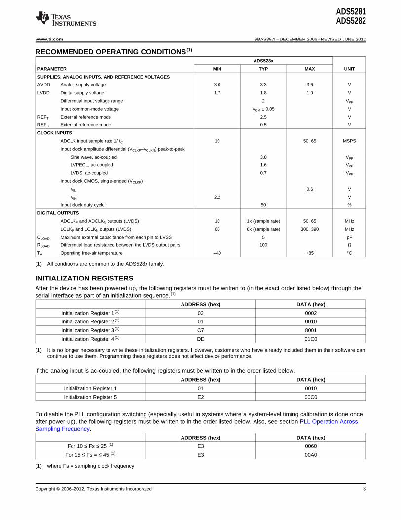
ADS5281ADS5282
wwwticom SBAS397I ndashDECEMBER 2006ndashREVISED JUNE 2012
RECOMMENDED OPERATING CONDITIONS (1)
ADS528x
PARAMETER MIN TYP MAX UNIT
SUPPLIES ANALOG INPUTS AND REFERENCE VOLTAGES
AVDD Analog supply voltage 30 33 36 V
LVDD Digital supply voltage 17 18 19 V
Differential input voltage range 2 VPP
Input common-mode voltage VCM plusmn 005 V
REFT External reference mode 25 V
REFB External reference mode 05 V
CLOCK INPUTS
ADCLK input sample rate 1 tC 10 50 65 MSPS
Input clock amplitude differential (VCLKPndashVCLKN) peak-to-peak
Sine wave ac-coupled 30 VPP
LVPECL ac-coupled 16 VPP
LVDS ac-coupled 07 VPP
Input clock CMOS single-ended (VCLKP)
VIL 06 V
VIH 22 V
Input clock duty cycle 50
DIGITAL OUTPUTS
ADCLKP and ADCLKN outputs (LVDS) 10 1x (sample rate) 50 65 MHz
LCLKP and LCLKN outputs (LVDS) 60 6x (sample rate) 300 390 MHz
CLOAD Maximum external capacitance from each pin to LVSS 5 pF
RLOAD Differential load resistance between the LVDS output pairs 100 Ω
TA Operating free-air temperature ndash40 +85 degC
(1) All conditions are common to the ADS528x family
INITIALIZATION REGISTERSAfter the device has been powered up the following registers must be written to (in the exact order listed below) through theserial interface as part of an initialization sequence (1)
ADDRESS (hex) DATA (hex)
Initialization Register 1 (1) 03 0002
Initialization Register 2 (1) 01 0010
Initialization Register 3 (1) C7 8001
Initialization Register 4 (1) DE 01C0
(1) It is no longer necessary to write these initialization registers However customers who have already included them in their software cancontinue to use them Programming these registers does not affect device performance
If the analog input is ac-coupled the following registers must be written to in the order listed below
ADDRESS (hex) DATA (hex)
Initialization Register 1 01 0010
Initialization Register 5 E2 00C0
To disable the PLL configuration switching (especially useful in systems where a system-level timing calibration is done onceafter power-up) the following registers must be written to in the order listed below Also see section PLL Operation AcrossSampling Frequency
ADDRESS (hex) DATA (hex)
For 10 le Fs le 25 (1) E3 0060
For 15 le Fs = le 45 (1) E3 00A0
(1) where Fs = sampling clock frequency
Copyright copy 2006ndash2012 Texas Instruments Incorporated 3
ADS5281ADS5282
SBAS397I ndashDECEMBER 2006ndashREVISED JUNE 2012 wwwticom
DIGITAL CHARACTERISTICSDC specifications refer to the condition where the digital outputs are not switching but are permanently at a valid logic level0 or 1 At CLOAD = 5pF (1) IOUT = 35mA (2) RLOAD = 100Ω (2) and no internal termination unless otherwise noted
ADS528x
PARAMETER TEST CONDITIONS MIN TYP MAX UNIT
DIGITAL INPUTS
High-level input voltage 14 V
Low-level input voltage 03 V
High-level input current 33 μA
Low-level input current ndash33 μA
Input capacitance 3 pF
LVDS OUTPUTS
High-level output voltage 1375 mV
Low-level output voltage 1025 mV
Output differential voltage |VOD| 350 mV
VOS output offset voltage Common-mode voltage of OUTP and OUTN 1200 mV
Output capacitance inside the device from eitherOutput capacitance 2 pFoutput to ground
(1) CLOAD is the effective external single-ended load capacitance between each output pin and ground(2) IOUT refers to the LVDS buffer current setting RLOAD is the differential load resistance between the LVDS output pair
4 Copyright copy 2006ndash2012 Texas Instruments Incorporated
ADS5281ADS5282
wwwticom SBAS397I ndashDECEMBER 2006ndashREVISED JUNE 2012
ELECTRICAL CHARACTERISTICS (1)
Typical values at +25degC Minimum and maximum values are measured across the specified temperature range of TMIN =ndash40degC to TMAX = +85degC AVDD = 33V LVDD = 18V clock frequency = 10MSPS to 65MSPS 50 clock duty cycle ndash1dBFSdifferential analog input internal reference mode ISET resistor = 562kΩ and LVDS buffer current setting = 35mA unlessotherwise noted
ADS528x
PARAMETER TEST CONDITIONS MIN TYP MAX UNIT
INTERNAL REFERENCE VOLTAGES
VREFB Reference bottom 05 V
VREFT Reference top 25 V
VREFT ndash VREFB 195 20 205 V
VCM Common-mode voltage (internal) 1425 15 1575 V
VCM output current plusmn2 mA
EXTERNAL REFERENCE VOLTAGES
VREFB Reference bottom 04 05 06 V
VREFT Reference top 24 25 26 V
VREFT ndash VREFB 19 20 21 V
ANALOG INPUT
Differential input voltage range 20 VPP
Differential input capacitance 3 pF
Analog input bandwidth 520 MHz
Analog input common-mode range DC-coupled input VCM plusmn 005 V
Per input pin per MSPS of sampling μAMHzAnalog input common-mode current 25speed per pin
Recovery from 6dB overload to within 1Voltage overload recovery time 1 Clock cycleaccuracy
Standard deviation seen on a periodicVoltage overload recovery repeatability first data within full-scale range in a 6dB 1 LSB
overloaded sine wave
DC ACCURACY
Offset error ndash125 plusmn02 +125 FS
Offset error temperature coefficient (2) plusmn5 ppmdegC
Channel gain error Excludes error in internal reference ndash08 FS
Channel gain error temperature Excludes temperature coefficient of plusmn10 ppmdegCcoefficient internal reference
Internal reference error temperature plusmn15 ppmdegCcoefficient (3)
DC PSRR DC power-supply rejection ratio (4) 15 mVV
POWER-DOWN MODES
Power in complete power-down mode 45 mW
Power in partial power-down mode Clock at 65MSPS 135 mW
Power with no clock 88 mW
DYNAMIC PERFORMANCE
5MHz full-scale signal applied to sevenCrosstalk channels measurement taken on channel ndash90 dBc
with no input signal
Two-tone third-order intermodulation f1 = 95MHz at ndash7dBFs ndash92 dBFSdistortion f2 = 102MHz at ndash7dBFs
(1) All characteristics are common for the ADS528x family(2) The offset temperature coefficient in ppmdegC is defined as (O1 ndash O2) times 106(T1 ndash T2)4096 where O1 and O2 are the offset codes in LSB
at the two extreme temperatures T1 and T2(3) The internal reference temperature coefficient is defined as (REF1 ndash REF2) times 106(T1 ndash T2)2 where REF1 and REF2 are the internal
reference voltages (VREFT ndash VREFB) at the two extreme temperatures T1 and T2(4) DC PSRR is defined as the ratio of the change in the ADC output (expressed in mV) to the change in supply voltage (in volts)
Copyright copy 2006ndash2012 Texas Instruments Incorporated 5
ADS5281ADS5282
SBAS397I ndashDECEMBER 2006ndashREVISED JUNE 2012 wwwticom
ELECTRICAL CHARACTERISTICS (BY DEVICE) (1)
Typical values at +25degC Minimum and maximum values are measured across the specified temperature range of TMIN =ndash40degC to TMAX = +85degC AVDD = 33V LVDD = 18V clock frequency = 10MSPS to 65MSPS 50 clock duty cycle ndash1dBFSdifferential analog input internal reference mode ISET resistor = 562kΩ and LVDS buffer current setting = 35mA unlessotherwise noted
ADS5281 ADS5281 ADS5282HTQFP-80 QFN-64 QFN-6450MSPS 50MSPS 65MSPS
PARAMETER TEST CONDITIONS MIN TYP MAX MIN TYP MAX MIN TYP MAX UNIT
DC ACCURACY
No missing codes Assured Assured Assured
DNL Differential nonlinearity ndash075 plusmn025 +075 ndash075 plusmn025 +075 ndash09 plusmn03 +09 LSB
INL Integral nonlinearity ndash15 plusmn07 +15 ndash15 plusmn07 +15 ndash17 plusmn07 +17 LSB
POWER SUPPLYmdashINTERNAL REFERENCE MODE
IAVDD Analog supply current 119 145 119 145 145 170 mA
ILVDD Digital current Zero input to all channels 76 95 76 95 89 102 mA
Total power 530 6495 530 6495 639 7446 mW
Obtained on powering down oneIncremental power saving 51 51 63 mW
channel at a time
POWER SUPPLYmdashEXTERNAL REFERENCE MODE
IAVDD Analog supply current 113 113 138 mA
ILVDD Digital current Zero input to all channels 76 76 89 mA
Total power 510 510 616 mW
Obtained on powering down oneIncremental power saving 50 50 61 mW
channel at a time
EXTERNAL REFERENCE LOADING
Current drawn by the eight ADCsfrom the external reference
Switching current 25 25 35 mAvoltages sourcing for REFT
sinking for REFB
DYNAMIC CHARACTERISTICS
fIN = 5MHz single-ended clock 74 85 74 85 72 85 dBcSFDR Spurious-free dynamic range
fIN = 30MHz differential clock 80 80 80 dBc
fIN = 5MHz single-ended clock 74 85 74 85 72 85 dBcHD2 Magnitude of second harmonic
fIN = 30MHz differential clock 82 82 82 dBc
fIN = 5MHz single-ended clock 74 85 74 85 72 85 dBcHD3 Magnitude of third harmonic
fIN = 30MHz differential clock 80 80 80 dBc
fIN = 5MHz single-ended clock 71 80 71 80 70 80THD Total harmonic distortion
fIN = 30MHz differential clock 78 78 78
fIN = 5MHz single-ended clock 683 70 683 70 683 70 dBFSSNR Signal-to-noise ratio
fIN = 30MHz differential clock 698 698 698 dBFS
fIN = 5MHz single-ended clock 677 697 677 697 673 697 dBFSSINAD Signal-to-noise and distortion
fIN = 30MHz differential clock 695 695 695 dBFS
(1) All characteristics are specific to each grade
6 Copyright copy 2006ndash2012 Texas Instruments Incorporated
60
59
58
57
56
55
54
53
52
51
50
49
48
47
46
45
44
43
42
41
AVDD
IN8N
IN8P
AVSS
IN7N
IN7P
AVDD
AVSS
IN6N
IN6P
AVSS
IN5N
IN5P
AVDD
LVSS
RESET
LVSS
LVSS
ADCLKN
ADCLKP
AV
SS
OU
T1
P
AV
SS
OU
T1
N
SC
LK
OU
T2
P
SD
ATA
OU
T2
N
CS
LV
DD
AV
DD
LV
SS
AV
SS
OU
T3
P
AV
SS
OU
T3
N
CLK
NO
UT
4P
CLK
PO
UT
4N
AV
DD
OU
T5
P
INT
EX
TO
UT
5N
AV
SS
OU
T6
P
RE
FT
OU
T6
N
RE
FB
LV
DD
VC
MLV
SS
I SE
TO
UT
7P
AV
DD
OU
T7
N
NC
OU
T8
P
TP
OU
T8
N
1
2
3
4
5
6
7
8
9
10
11
12
13
14
15
16
17
18
19
20
AVDD
IN1P
IN1N
AVSS
IN2P
IN2N
AVDD
AVSS
IN3P
IN3N
AVSS
IN4P
IN4N
AVDD
LVSS
PD
LVSS
LVSS
LCLKP
LCLKN
80 79 78 77 76 75 74 73 72 71 70
21 22 23 24 25 26 27 28 29 30 31
69
32 33 34 35 36 37 38 39 40
68 67 66 65 64 63 62 61
ADS528x
ADS5281ADS5282
wwwticom SBAS397I ndashDECEMBER 2006ndashREVISED JUNE 2012
PIN CONFIGURATIONS
TQFP-80TOP VIEW
Table 2 PIN DESCRIPTIONS TQFP-80
PIN NAME DESCRIPTION PIN NUMBER OF PINS
ADCLKN LVDS frame clock (1X)mdashnegative output 42 1
ADCLKP LVDS frame clock (1X)mdashpositive output 41 1
AVDD Analog power supply 33V 1 7 14 47 54 60 63 70 75 9
AVSS Analog ground 4 8 11 50 53 57 68 73 74 79 80 11
Negative differential clockCLKN 72 1Tie CLKN to 0V for a single-ended clock
CLKP Positive differential clock 71 1
CS Serial enable chip selectmdashactive low digital input 76 1
IN1N Negative differential input signal channel 1 3 1
IN1P Positive differential input signal channel 1 2 1
IN2N Negative differential input signal channel 2 6 1
Copyright copy 2006ndash2012 Texas Instruments Incorporated 7
ADS5281ADS5282
SBAS397I ndashDECEMBER 2006ndashREVISED JUNE 2012 wwwticom
Table 2 PIN DESCRIPTIONS TQFP-80 (continued)
PIN NAME DESCRIPTION PIN NUMBER OF PINS
IN2P Positive differential input signal channel 2 5 1
IN3N Negative differential input signal channel 3 10 1
IN3P Positive differential input signal channel 3 9 1
IN4N Negative differential input signal channel 4 13 1
IN4P Positive differential input signal channel 4 12 1
IN5N Negative differential input signal channel 5 49 1
IN5P Positive differential input signal channel 5 48 1
IN6N Negative differential input signal channel 6 52 1
IN6P Positive differential input signal channel 6 51 1
IN7N Negative differential input signal channel 7 56 1
IN7P Positive differential input signal channel 7 55 1
IN8N Negative differential input signal channel 8 59 1
IN8P Positive differential input signal channel 8 58 1
INTEXT Internalexternal reference mode select input 69 1
ISET Bias pinmdash562kΩ to ground 64 1
LCLKN LVDS bit clock (6X)mdashnegative output 20 1
LCLKP LVDS bit clock (6X)mdashpositive output 19 1
LVDD Digital and IO power supply 18V 25 35 2
LVSS Digital ground 15 17 18 26 36 43 44 46 8
NC No connection (or connect to ground) 62 1
OUT1N LVDS channel 1mdashnegative output 22 1
OUT1P LVDS channel 1mdashpositive output 21 1
OUT2N LVDS channel 2mdashnegative output 24 1
OUT2P LVDS channel 2mdashpositive output 23 1
OUT3N LVDS channel 3mdashnegative output 28 1
OUT3P LVDS channel 3mdashpositive output 27 1
OUT4N LVDS channel 4mdashnegative output 30 1
OUT4P LVDS channel 4mdashpositive output 29 1
OUT5N LVDS channel 5mdashnegative output 32 1
OUT5P LVDS channel 5mdashpositive output 31 1
OUT6N LVDS channel 6mdashnegative output 34 1
OUT6P LVDS channel 6mdashpositive output 33 1
OUT7N LVDS channel 7mdashnegative output 38 1
OUT7P LVDS channel 7mdashpositive output 37 1
OUT8N LVDS channel 8mdashnegative output 40 1
OUT8P LVDS channel 8mdashpositive output 39 1
PD Power-down input 16 1
REFB Negative reference inputoutput 66 1
REFT Positive reference inputoutput 67 1
RESET Active low RESET input 45 1
SCLK Serial clock input 78 1
SDATA Serial data input 77 1
TP Test pin do not use 61 1
VCM Common-mode output pin 15V output 65 1
8 Copyright copy 2006ndash2012 Texas Instruments Incorporated
48
47
46
45
44
43
42
41
40
39
38
37
36
35
34
33
IN8N
IN8P
AVSS
IN7N
IN7P
AVSS
IN6N
IN6P
AVSS
IN5N
IN5P
AVSS
LVSS
LVDD
OUT8N
OUT8P
1
2
3
4
5
6
7
8
9
10
11
12
13
14
15
16
IN1P
IN1N
AVSS
IN2P
IN2N
AVSS
IN3P
IN3N
AVSS
IN4P
IN4N
LVSS
PD
LVSS
OUT1P
OUT1N
RE
SE
T
SC
LK
SD
ATA
CS
AV
DD
CLK
N
CLK
P
AV
DD
INT
EX
T
RE
FT
RE
FB
VC
M
TP
I SE
T
AV
DD
AV
DD
OU
T2
P
OU
T2
N
OU
T3
P
OU
T3
N
OU
T4
P
OU
T4
N
AD
CLK
P
AD
CLK
N
LC
LK
P
LC
LK
N
OU
T5
P
OU
T5
N
OU
T6
P
OU
T6
N
OU
T7
P
OU
T7
N
64 63 62 61 60 59 58 57 56 55 54
17 18 19 20 21 22 23 24 25 26 27
53 52 51 50 49
28 29 30 31 32
ADS528X
ADS5281ADS5282
wwwticom SBAS397I ndashDECEMBER 2006ndashREVISED JUNE 2012
QFN-64 PowerPADTOP VIEW
Table 3 PIN DESCRIPTIONS QFN-64
PIN NAME DESCRIPTION PIN NUMBER OF PINS
ADCLKN LVDS frame clock (1X)mdashnegative output 24 1
ADCLKP LVDS frame clock (1X)mdashpositive output 23 1
AVDD Analog power supply 33V 49 50 57 60 4
AVSS Analog ground 3 6 9 37 40 43 46 7
Negative differential clock inputCLKN 59 1Tie CLKN to 0V for a single-ended clock
CLKP Positive differential clock input 58 1
CS Serial enable chip selectmdashactive low digital input 61 1
IN1N Negative differential input signal channel 1 2 1
IN1P Positive differential input signal channel 1 1 1
IN2N Negative differential input signal channel 2 5 1
IN2P Positive differential input signal channel 2 4 1
IN3N Negative differential input signal channel 3 8 1
IN3P Positive differential input signal channel 3 7 1
IN4N Negative differential input signal channel 4 11 1
IN4P Positive differential input signal channel 4 10 1
IN5N Negative differential input signal channel 5 39 1
Copyright copy 2006ndash2012 Texas Instruments Incorporated 9
ADS5281ADS5282
SBAS397I ndashDECEMBER 2006ndashREVISED JUNE 2012 wwwticom
Table 3 PIN DESCRIPTIONS QFN-64 (continued)
PIN NAME DESCRIPTION PIN NUMBER OF PINS
IN5P Positive differential input signal channel 5 38 1
IN6N Negative differential input signal channel 6 42 1
IN6P Positive differential input signal channel 6 41 1
IN7N Negative differential input signal channel 7 45 1
IN7P Positive differential input signal channel 7 44 1
IN8N Negative differential input signal channel 8 48 1
IN8P Positive differential input signal channel 8 47 1
INTEXT Internalexternal reference mode select input 56 1
ISET Bias pinmdash562kΩ to ground 51 1
LCLKN LVDS bit clock (6X)mdashnegative output 26 1
LCLKP LVDS bit clock (6X)mdashpositive output 25 1
LVDD Digital and IO power supply 18V 35 1
LVSS Digital ground 12 14 36 3
OUT1N LVDS channel 1mdashnegative output 16 1
OUT1P LVDS channel 1mdashpositive output 15 1
OUT2N LVDS channel 2mdashnegative output 18 1
OUT2P LVDS channel 2mdashpositive output 17 1
OUT3N LVDS channel 3mdashnegative output 20 1
OUT3P LVDS channel 3mdashpositive output 19 1
OUT4N LVDS channel 4mdashnegative output 22 1
OUT4P LVDS channel 4mdashpositive output 21 1
OUT5N LVDS channel 5mdashnegative output 28 1
OUT5P LVDS channel 5mdashpositive output 27 1
OUT6N LVDS channel 6mdashnegative output 30 1
OUT6P LVDS channel 6mdashpositive output 29 1
OUT7N LVDS channel 7mdashnegative output 32 1
OUT7P LVDS channel 7mdashpositive output 31 1
OUT8N LVDS channel 8mdashnegative output 34 1
OUT8P LVDS channel 8mdashpositive output 33 1
PD Power-down input 13 1
REFB Negative reference inputoutput 54 1
REFT Positive reference inputoutput 55 1
RESET Active low RESET input 64 1
SCLK Serial clock input 63 1
SDATA Serial data input 62 1
TP Test pin do not use 52 1
VCM Common-mode output pin 15V output 53 1
10 Copyright copy 2006ndash2012 Texas Instruments Incorporated
12-BitADC
PLL
Serializer
1x ADCLK
6x ADCLK
IN1P
IN1N
OUT1P
OUT1N
12-BitADC
SerializerIN2P
IN2N
OUT2P
OUT2N
12-BitADC
SerializerIN3P
IN3N
OUT3P
OUT3N
LCLKP
LCLKN
ADCLKP
ADCLKN
12x ADCLK
12-BitADC
SerializerIN4P
IN4N
OUT4P
OUT4N
12-BitADC
SerializerIN5P
IN5N
OUT5P
OUT5N
12-BitADC
SerializerIN6P
IN6N
OUT6P
OUT6N
12-BitADC
SerializerIN7P
IN7N
OUT7P
OUT7N
12-BitADC
Serializer
Digital
Digital
Digital
Digital
Digital
Digital
Digital
Digital
Reference
IN8P
IN8N
RE
FT
INT
EX
T
RE
FB
VC
M
OUT8P
OUT8N
I SE
T
Registers
SD
ATA
CS
RE
SE
T
SC
LK
ADC
Control
PD
Clock
Buffer
(AD
CL
K)
CL
KP
(AV
SS
)
CL
KN
AV
DD
(33
V)
LV
DD
(18
V)
Power-
Down
Te
st
Pa
tte
rns
Drive
Cu
rre
nt
Ou
tpu
t F
orm
at
Dig
ita
l G
ain
(0d
B-1
2d
B)
ADS5281ADS5282
wwwticom SBAS397I ndashDECEMBER 2006ndashREVISED JUNE 2012
FUNCTIONAL BLOCK DIAGRAM
Copyright copy 2006ndash2012 Texas Instruments Incorporated 11
tH1
tSU1
tH2
tSU2
LCLKN
LCLKP
OUTN
OUTP
D0 D1 D2 D3 D4 D5 D6 D7 D8 D9 D10 D11 D0 D1 D2 D3 D4 D5 D6 D7 D8 D9 D10 D11D0 D1 D2 D3 D4 D5 D6 D7 D8 D9 D10 D11
Sample nSample n + 12
tPROP
t (A)D
12 clocks latency
Analog Input
Clock Input
6X ADCLK
LCLKN
LCLKP
1X ADCLK
ADCLKN
ADCLKP
SERIAL DATA
OUTP
OUTN
tSAMPLE
Sample n + 13
ADS5281ADS5282
SBAS397I ndashDECEMBER 2006ndashREVISED JUNE 2012 wwwticom
LVDS TIMING DIAGRAM
DEFINITION OF SETUP AND HOLD TIMES
tSU = min(tSU1 tSU2)
tH = min(tH1 tH2)
TIMING CHARACTERISTICS (1) (2)
ADS528x
PARAMETER TEST CONDITIONS MIN TYP MAX UNIT
tA Aperture delay 15 45 ns
Aperture delay variation Channel-to-channel within the same device (3σ) plusmn20 ps
tJ Aperture jitter 400 fs
Time to valid data after coming out of 50 μsCOMPLETE POWER-DOWN mode
Time to valid data after coming out of PARTIALtWAKE Wake-up time POWER-DOWN mode (with clock continuing to 2 μs
run during power-down)
Time to valid data after stopping and restarting 40 μsthe input clock
ClockData latency 12 cycles
(1) Timing characteristics are common to the ADS528x family(2) Timing parameters are ensured by design and characterization not production tested
12 Copyright copy 2006ndash2012 Texas Instruments Incorporated
ADS5281ADS5282
wwwticom SBAS397I ndashDECEMBER 2006ndashREVISED JUNE 2012
LVDS OUTPUT TIMING CHARACTERISTICS (1) (2)
Typical values are at +25degC minimum and maximum values are measured across the specified temperature range of TMIN = ndash40degC to TMAX =+85degC sampling frequency = as specified CLOAD = 5pF (3) IOUT = 35mA RLOAD = 100Ω (4) and no internal termination unless otherwisenoted
ADS528x
40MSPS 50MSPS 65MSPS
PARAMETER TEST CONDITIONS (5) MIN TYP MAX MIN TYP MAX MIN TYP MAX UNIT
Data valid (7) to zero-crossing oftSU Data setup time(6) 067 047 027 ns
LCLKP
Zero-crossing of LCLKP to datatH Data hold time(6) 085 065 04 ns
becoming invalid(7)
Input clock (ADCLK) rising edgetPROP Clock propagation delay cross-over to output clock (ADCLKP) 10 14 166 10 125 141 97 115 14 ns
rising edge cross-over
Duty cycle of differential clockLVDS bit clock duty cycle 455 50 53 45 50 535 41 50 57
(LCLKP ndash LCLKN)
Bit clock cycle-to-cycle250 250 250 ps pp
jitter
Frame clock cycle-to-cycle150 150 150 ps pp
jitter
tRISE Data rise time data fall Rise time is from ndash100mV to +100mV009 02 04 009 02 04 009 02 04 ns
tFALL time Fall time is from +100mV to ndash100mV
tCLKRISE Output clock rise time Rise time is from ndash100mV to +100mV009 02 04 009 02 04 009 02 04 ns
tCLKFALL output clock fall time Fall time is from +100mV to ndash100mV
(1) All characteristics are at the maximum rated speed for each speed grade(2) Timing parameters are ensured by design and characterization not production tested(3) CLOAD is the effective external single-ended load capacitance between each output pin and ground(4) IOUT refers to the LVDS buffer current setting RLOAD is the differential load resistance between the LVDS output pair(5) Measurements are done with a transmission line of 100Ω characteristic impedance between the device and the load(6) Setup and hold time specifications take into account the effect of jitter on the output data and clock These specifications also assume
that data and clock paths are perfectly matched within the receiver Any mismatch in these paths within the receiver would appear asreduced timing margin
(7) Data valid refers to a logic high of +100mV and a logic low of ndash100mV
LVDS OUTPUT TIMING CHARACTERISTICS (1) (2)
Typical values are at +25degC minimum and maximum values are measured across the specified temperature range of TMIN = ndash40degC to TMAX =+85degC sampling frequency = as specified CLOAD = 5pF (3) IOUT = 35mA RLOAD = 100Ω (4) and no internal termination unless otherwisenoted
ADS528x
30MSPS 20MSPS 10MSPS
PARAMETER TEST CONDITIONS (5) MIN TYP MAX MIN TYP MAX MIN TYP MAX UNIT
Data valid (7) to zero-crossing oftSU Data setup time(6) 08 15 37 ns
LCLKP
Zero-crossing of LCLKP to datatH Data hold time(6) 12 19 39 ns
becoming invalid(7)
Input clock (ADCLK) rising edgetPROP Clock propagation delay cross-over to output clock (ADCLKP) 95 135 173 95 145 173 10 147 171 ns
rising edge cross-over
Duty cycle of differential clockLVDS bit clock duty cycle 465 50 52 48 50 51 49 50 51
(LCLKP ndash LCLKN)
Bit clock cycle-to-cycle250 250 750 ps pp
jitter
Frame clock cycle-to-cycle150 150 500 ps pp
jitter
tRISE Data rise time data fall Rise time is from ndash100mV to +100mV009 02 04 009 02 04 009 02 04 ns
tFALL time Fall time is from +100mV to ndash100mV
tCLKRISE Output clock rise time Rise time is from ndash100mV to +100mV009 02 04 009 02 04 009 02 04 ns
tCLKFALL output clock fall time Fall time is from +100mV to ndash100mV
(1) All characteristics are at the speeds other than the maximum rated speed for each speed grade(2) Timing parameters are ensured by design and characterization not production tested(3) CLOAD is the effective external single-ended load capacitance between each output pin and ground(4) IOUT refers to the LVDS buffer current setting RLOAD is the differential load resistance between the LVDS output pair(5) Measurements are done with a transmission line of 100Ω characteristic impedance between the device and the load(6) Setup and hold time specifications take into account the effect of jitter on the output data and clock These specifications also assume
that data and clock paths are perfectly matched within the receiver Any mismatch in these paths within the receiver would appear asreduced timing margin
(7) Data valid refers to a logic high of +100mV and a logic low of ndash100mV
Copyright copy 2006ndash2012 Texas Instruments Incorporated 13
t1
t2
t3
AVDD (3V to 36V)
LVDD (17V to 19V)
High-Level RESET
(14V to 36V)
High-Level CS
(14V to 36V)
Device Ready for
Serial Register Write(2)
Device Ready for
Data ConversionStart of Clock
AVDD
LVDD
RESET
CS
ADCLK
t4 t7
t5
t8
t6
ADS5281ADS5282
SBAS397I ndashDECEMBER 2006ndashREVISED JUNE 2012 wwwticom
LVDS OUTPUT TIMING CHARACTERISTICSTIMINGS WHEN USING REGISTER 0xE3 (2)
At 40 MSPSPARAMETER (1) TEST CONDITIONS
MIN TYP MAX
Data setup time Data valid (3) to zero-crossing of LCLKp 060
Data hold time Zero-crossing of LCLKP to data becoming invalid(3) 092
Input clock (ADCLK) rising edge cross-over to output clock (ADCLK) rising edgeClock propagation delay 8 12 146
crossover
(1) Only the setup time hold time and clock propagation delay parameters are affected Rest of the parameters are same as given inprevious two tables
(2) Only timing specifications for 40MSPS are affected when using register 0xE3 (as specified in the recommended operating table section)The timing specifications for other clock frequencies are same as given in previous two tables
(3) Data valid refers to logic high of +100mV and logic low of ndash100mV
RECOMMENDED POWER-UP SEQUENCING AND RESET TIMING
10μs lt t1 lt 50ms 10μs lt t2 lt 50ms ndash10ms lt t3 lt 10ms t4 gt 10ms t5 gt 100ns t6 gt 100ns t7 gt 10ms and t8 gt 100μs
(1) The AVDD and LVDD power on sequence does not matter as long as ndash10ms lt t3 lt 10ms Similar considerations apply while shuttingdown the device
(2) Write initialization registers listed in the Initialization Registers table
14 Copyright copy 2006ndash2012 Texas Instruments Incorporated
PD
Device Fully
Powers DownDevice Fully
Powers Up
tWAKE1 sm
ADS5281ADS5282
wwwticom SBAS397I ndashDECEMBER 2006ndashREVISED JUNE 2012
POWER-DOWN TIMING
Power-up time shown is based on 1μF bypass capacitors on the reference pins tWAKE is the time it takes for the device to wake upcompletely from power-down mode The ADS528x has two power-down modes complete power-down mode and partial power-down modeThe device can be configured in partial power-down mode through a register setting
tWAKE lt 50μs for complete power-down mode
tWAKE lt 2μs for partial power-down mode (provided the clock is not shut off during power-down)
Copyright copy 2006ndash2012 Texas Instruments Incorporated 15
D15 D14 D13 D12 D11 D10 D9 D8 D7 D6 D5 D4 D3 D2 D1 D0A7 A6 A5 A4 A3 A2 A1 A0
CS
SCLK
SDATA
Data latched on rising edge of SCLK
Start Sequence End Sequence
t6
t4
t2
t7
t3
t5
t1
ADS5281ADS5282
SBAS397I ndashDECEMBER 2006ndashREVISED JUNE 2012 wwwticom
SERIAL INTERFACE
The ADS528x has a set of internal registers that can be accessed through the serial interface formed by pins CS(chip select active low) SCLK (serial interface clock) and SDATA (serial interface data) When CS is low thefollowing actions occurbull Serial shift of bits into the device is enabledbull SDATA (serial data) is latched at every rising edge of SCLKbull SDATA is loaded into the register at every 24th SCLK rising edge
If the word length exceeds a multiple of 24 bits the excess bits are ignored Data can be loaded in multiples of24-bit words within a single active CS pulse The first eight bits form the register address and the remaining 16bits form the register data The interface can work with SCLK frequencies from 20MHz down to very low speeds(a few hertz) and also with a non-50 SCLK duty cycle
Register Initialization
After power-up the internal registers must be initialized to the respective default values Initialization can bedone in one of two ways1 Through a hardware reset by applying a low-going pulse on the RESET pin or2 Through a software reset using the serial interface set the RST bit high Setting this bit initializes the
internal registers to the respective default values and then self-resets the RST bit low In this case theRESET pin stays high (inactive)
After all registers have been initialized to their default values through a RESET operation the registers detailedin the Initialization Registers table must be written into This process must be done after every hardware orsoftware RESET operation in order to reconfigure the device for the best mode of operation
SERIAL INTERFACE TIMING
ADS528x
PARAMETER DESCRIPTION MIN TYP MAX UNIT
t1 SCLK period 50 ns
t2 SCLK high time 20 ns
t3 SCLK low time 20 ns
t4 Data setup time 5 ns
t5 Data hold time 5 ns
t6 CS fall to SCLK rise 8 ns
t7 Time between last SCLK rising edge to CS rising edge 8 ns
16 Copyright copy 2006ndash2012 Texas Instruments Incorporated
ADS5281ADS5282
wwwticom SBAS397I ndashDECEMBER 2006ndashREVISED JUNE 2012
SERIAL REGISTER MAP
Table 4 SUMMARY OF FUNCTIONS SUPPORTED BY SERIAL INTERFACE (1) (2) (3) (4)
ADDRESSIN HEX D15 D14 D13 D12 D11 D10 D9 D8 D7 D6 D5 D4 D3 D2 D1 D0 NAME DESCRIPTION DEFAULT
00 X RST Self-clearing software RESET Inactive
Channel-specific ADC power-X X X X X X X X PDN_CHlt81gt Inactive
down mode
Partial power-down mode (fastX PDN_PARTIAL Inactive
recovery from power-down)0F
Register mode for completeX PDN_COMPLETE Inactive
power-down (slower recovery)
Configures the PD pin for partial CompleteX PDN_PIN_CFG
power-down mode power-down
LVDS current driveX X X ILVDS_LCLKlt20gt programmability for LCLKN and 35mA drive
LCLKP pins
LVDS current driveILVDS_FRAME
11 X X X programmability for ADCLKN and 35mA drivelt20gt
ADCLKP pins
LVDS current driveX X X ILVDS_DATlt20gt programmability for OUTN and 35mA drive
OUTP pins
Enables internal termination for TerminationX EN_LVDS_TERM
LVDS buffers disabled
Programmable termination for Termination1 X X X TERM_LCLKlt20gt
LCLKN and LCLKP buffers disabled12
TERM_FRAME Programmable termination for Termination1 X X X
lt20gt ADCLKN and ADCLKP buffers disabled
Programmable termination for Termination1 X X X TERM_DATlt20gt
OUTN and OUTP buffers disabled
Channel-specific low-frequency14 X X X X X X X X LFNS_CHlt81gt Inactive
noise suppression mode enable
INP isSwaps the polarity of the analog
24 X X X X X X X X INVERT_CHlt81gt positiveinput pins electrically
input
Enables a repeating full-scaleX 0 0 EN_RAMP Inactive
ramp pattern on the outputs
Enables the mode wherein theDUALCUSTOM_
0 X 0 output toggles between two InactivePAT
defined codes
Enables the mode wherein theSINGLE_CUSTOM
0 0 X output is a constant specified Inactive25 _PAT
code
2MSBs for a single customBITS_CUSTOM1 pattern (and for the first code of
X X Inactivelt1110gt the dual custom pattern) lt11gt is
the MSB
BITS_CUSTOM2 2MSBs for the second code ofX X Inactive
lt1110gt the dual custom pattern
10 lower bits for the singleBITS_CUSTOM1 custom pattern (and for the first
26 X X X X X X X X X X Inactivelt90gt code of the dual custom pattern)
lt0gt is the LSB
BITS_CUSTOM2 10 lower bits for the second27 X X X X X X X X X X Inactive
lt90gt code of the dual custom pattern
X X X X GAIN_CH1lt30gt Programmable gain channel 1 0dB gain
X X X X GAIN_CH2lt30gt Programmable gain channel 2 0dB gain2A
X X X X GAIN_CH3lt30gt Programmable gain channel 3 0dB gain
X X X X GAIN_CH4lt30gt Programmable gain channel 4 0dB gain
X X X X GAIN_CH5lt30gt Programmable gain channel 5 0dB gain
X X X X GAIN_CH6lt30gt Programmable gain channel 6 0dB gain2B
X X X X GAIN_CH7lt30gt Programmable gain channel 7 0dB gain
X X X X GAIN_CH8lt30gt Programmable gain channel 8 0dB gain
(1) The unused bits in each register (identified as blank table cells) must be programmed as 0(2) X = Register bit referenced by the corresponding name and description (default is 0)(3) Bits marked as 0 should be forced to 0 and bits marked as 1 should be forced to 1 when the particular register is programmed(4) Multiple functions in a register should be programmed in a single write operation
Copyright copy 2006ndash2012 Texas Instruments Incorporated 17
ADS5281ADS5282
SBAS397I ndashDECEMBER 2006ndashREVISED JUNE 2012 wwwticom
Table 4 SUMMARY OF FUNCTIONS SUPPORTED BY SERIAL INTERFACE(1) (2) (3) (4) (continued)ADDRESS
IN HEX D15 D14 D13 D12 D11 D10 D9 D8 D7 D6 D5 D4 D3 D2 D1 D0 NAME DESCRIPTION DEFAULT
Single-1 X DIFF_CLK Differential clock mode
ended clock
Enables the duty-cycle correction1 X EN_DCC Disabled
circuit
External42Drives the external reference reference
1 X EXT_REF_VCMmode through the VCM pin drives REFT
and REFB
Controls the phase of LCLK1 X X PHASE_DDRlt10gt 90 degrees
output relative to data
0 X PAT_DESKEW Enables deskew pattern mode Inactive45
X 0 PAT_SYNC Enables sync pattern mode Inactive
Binary twos complement format Straight1 1 X BTC_MODE
for ADC output offset binary
Serialized ADC output comes LSB-first1 1 X MSB_FIRST
out MSB-first output
Enables SDR output modeDDR output46 1 1 X EN_SDR (LCLK becomes a 12x input
modeclock)
Controls whether the LCLK rising Rising edgeor falling edge comes in the of LCLK in
1 X 1 1 FALL_SDRmiddle of the data window when middle ofoperating in SDR output mode data window
SUMMARY OF FEATURES
POWER IMPACT (relative to default)FEATURES DEFAULT SELECTION AT fS = 65MSPS
ANALOG FEATURES
Internal or external reference Internal reference mode uses approximately 23mW moreNA Pin(driven on the REFT and REFB pins) power on AVDD
External reference driven on the Off Register 42 Approximately 9mW less power on AVDDVCM pin
Duty cycle correction circuit Off Register 42 Approximately 7mW more power on AVDD
With zero input to the ADC low-frequency noise suppressionLow-frequency noise suppression Off Register 14 causes digital switching at fS2 thereby increasing LVDD
power by approximately 7mWchannel
Differential clock mode uses approximately 7mW more powerSingle-ended or differential clock Single-ended Register 42 on AVDD
Refer to the Power-Down Modes section in the ElectricalPower-down mode Off Pin and register 0F Characteristics table
DIGITAL FEATURES
Programmable digital gain (0dB to Registers 2A and0dB No difference12dB) 2B
Straight offset or BTC output Straight offset Register 46 No difference
Swap polarity of analog input pins Off Register 24 No difference
LVDS OUTPUT PHYSICAL LAYER
LVDS internal termination Off Register 12 Approximately 7mW more power on AVDD
LVDS current programmability 35mA Register 11 As per LVDS clock and data buffer current setting
LVDS OUTPUT TIMING
LSB- or MSB-first output LSB-first Register 46 No difference
SDR mode uses approximately 2mW more power on LVDDDDR or SDR output DDR Register 46 (at fS = 30MSPS)
Refer toLCLK phase relative to data output Register 42 No differenceFigure 1
18 Copyright copy 2006ndash2012 Texas Instruments Incorporated
ADS5281ADS5282
wwwticom SBAS397I ndashDECEMBER 2006ndashREVISED JUNE 2012
DESCRIPTION OF SERIAL REGISTERS
SOFTWARE RESET
ADDRESSIN HEX D15 D14 D13 D12 D11 D10 D9 D8 D7 D6 D5 D4 D3 D2 D1 D0 NAME
00 X RST
Software reset is applied when the RST bit is set to 1 setting this bit resets all internal registers and self-clearsto 0
POWER-DOWN MODES
ADDRESSIN HEX D15 D14 D13 D12 D11 D10 D9 D8 D7 D6 D5 D4 D3 D2 D1 D0 NAME
X X X X X X X X PDN_CHlt81gt
X PDN_PARTIAL0F
0 X PDN_COMPLETE
X 0 PDN_PIN_CFG
Each of the eight channels can be individually powered down PDN_CHltNgt controls the power-down mode forthe ADC channel ltNgt
In addition to channel-specific power-down the ADS528x also has two global power-down modesmdashpartialpower-down mode and complete power-down mode Partial power-down mode partially powers down the chiprecovery from this mode is much quicker provided that the clock has been running for at least 50μs beforeexiting this mode Complete power-down mode on the other hand completely powers down the chip andinvolves a much longer recovery time
In addition to programming the device for either of these two power-down modes (through either thePDN_PARTIAL or PDN_COMPLETE bits respectively) the PD pin itself can be configured as either a partialpower-down pin or a complete power-down pin control For example if PDN_PIN_CFG = 0 (default) when thePD pin is high the device enters complete power-down mode However if PDN_PIN_CFG = 1 when the PD pinis high the device enters partial power-down mode
LVDS DRIVE PROGRAMMABILITY
ADDRESSIN HEX D15 D14 D13 D12 D11 D10 D9 D8 D7 D6 D5 D4 D3 D2 D1 D0 NAME
X X X ILVDS_LCLKlt20gt
11 X X X ILVDS_FRAMElt20gt
X X X ILVDS_DATlt20gt
The LVDS drive strength of the bit clock (LCLKP or LCLKN) and the frame clock (ADCLKP or ADCLKN) can beindividually programmed The LVDS drive strengths of all the data outputs OUTP and OUTN can also beprogrammed to the same value
Copyright copy 2006ndash2012 Texas Instruments Incorporated 19
ADS5281ADS5282
SBAS397I ndashDECEMBER 2006ndashREVISED JUNE 2012 wwwticom
All three drive strengths (bit clock frame clock and data) are programmed using sets of three bits Table 5shows an example of how the drive strength of the bit clock is programmed (the method is similar for the frameclock and data drive strengths)
Table 5 Bit Clock Drive Strength (1)
ILVDS_LCLKlt2gt ILVDS_LCLKlt1gt ILVDS_LCLKlt0gt LVDS DRIVE STRENGTH FOR LCLKP AND LCLKN
0 0 0 35mA (default)
0 0 1 25mA
0 1 0 15mA
0 1 1 05mA
1 0 0 75mA
1 0 1 65mA
1 1 0 55mA
1 1 1 45mA
(1) Current settings lower than 15mA are not recommended
LVDS INTERNAL TERMINATION PROGRAMMABILITY
ADDRESSIN HEX D15 D14 D13 D12 D11 D10 D9 D8 D7 D6 D5 D4 D3 D2 D1 D0 NAME
X EN_LVDS_TERM
1 X X X TERM_LCLKlt20gt12
1 X X X TERM_FRAMElt20gt
1 X X X TERM_DATlt20gt
The LVDS buffers have high-impedance current sources driving the outputs When driving traces whosecharacteristic impedance is not perfectly matched with the termination impedance on the receiver side there maybe reflections back to the LVDS output pins of the ADS528x that cause degraded signal integrity By enabling aninternal termination (between the positive and negative outputs) for the LVDS buffers the signal integrity can besignificantly improved in such scenarios To set the internal termination mode the EN_LVDS_TERM bit shouldbe set to 1 Once this bit is set the internal termination values for the bit clock frame clock and data bufferscan be independently programmed using sets of three bits Table 6 shows an example of how the internaltermination of the LVDS buffer driving the bit clock is programmed (the method is similar for the frame clock anddata buffers) These termination values are only typical values and can vary by up to plusmn20 across temperatureand from device to device
Table 6 Bit Clock Internal Termination
INTERNAL TERMINATION BETWEENTERM_LCLKlt2gt TERM_LCLKlt1gt TERM_LCLKlt0gt LCLKP AND LCLKN IN Ω
0 0 0 None
0 0 1 260
0 1 0 150
0 1 1 94
1 0 0 125
1 0 1 80
1 1 0 66
1 1 1 55
20 Copyright copy 2006ndash2012 Texas Instruments Incorporated
ADS5281ADS5282
wwwticom SBAS397I ndashDECEMBER 2006ndashREVISED JUNE 2012
LOW-FREQUENCY NOISE SUPPRESSION MODE
ADDRESSIN HEX D15 D14 D13 D12 D11 D10 D9 D8 D7 D6 D5 D4 D3 D2 D1 D0 NAME
14 X X X X X X X X LFNS_CHlt81gt
The low-frequency noise suppression mode is specifically useful in applications where good noise performance isdesired in the frequency band of 0MHz to 1MHz (around dc) Setting this mode shifts the low-frequency noise ofthe ADS528x to approximately fS2 thereby moving the noise floor around dc to a much lower valueLFNS_CHlt81gt enables this mode individually for each channel
ANALOG INPUT INVERT
ADDRESSIN HEX D15 D14 D13 D12 D11 D10 D9 D8 D7 D6 D5 D4 D3 D2 D1 D0 NAME
24 X X X X X X X X INVERT_CHlt81gt
Normally the INP pin represents the positive analog input pin and INN represents the complementary negativeinput Setting the bits marked INVERT_CHlt81gt (individual control for each channel) causes the inputs to beswapped INN now represents the positive input and INP the negative input
LVDS TEST PATTERNS
ADDRESSIN HEX D15 D14 D13 D12 D11 D10 D9 D8 D7 D6 D5 D4 D3 D2 D1 D0 NAME
X 0 0 EN_RAMP
0 X 0 DUALCUSTOM_PAT
25 0 0 X SINGLE_CUSTOM_PAT
X X BITS_CUSTOM1lt1110gt
X X BITS_CUSTOM2lt1110gt
26 X X X X X X X X X X BITS_CUSTOM1lt90gt
27 X X X X X X X X X X BITS_CUSTOM2lt90gt
0 X PAT_DESKEW45
X 0 PAT_SYNC
The ADS528x can output a variety of test patterns on the LVDS outputs These test patterns replace the normalADC data output Setting EN_RAMP to 1 causes all the channels to output a repeating full-scale ramp patternThe ramp increments from zero code to full-scale code in steps of 1LSB every clock cycle After hitting the full-scale code it returns back to zero code and ramps again
The device can also be programmed to output a constant code by setting SINGLE_CUSTOM_PAT to 1 andprogramming the desired code in BITS_CUSTOM1lt110gt In this mode BITS_CUSTOM1lt110gt take the placeof the 12-bit ADC data at the output and are controlled by LSB-first and MSB-first modes in the same way asnormal ADC data are
The device may also be made to toggle between two consecutive codes by programming DUAL_CUSTOM_PATto 1 The two codes are represented by the contents of BITS_CUSTOM1lt110gt and BITS_CUSTOM2lt110gt
In addition to custom patterns the device may also be made to output two preset patterns1 Deskew patten Set using PAT_DESKEW this mode replaces the 12-bit ADC output Dlt110gt with the
010101010101 word2 Sync pattern Set using PAT_SYNC the normal ADC word is replaced by a fixed 111111000000 word
Note that only one of the above patterns should be active at any given instant
Copyright copy 2006ndash2012 Texas Instruments Incorporated 21
ADS5281ADS5282
SBAS397I ndashDECEMBER 2006ndashREVISED JUNE 2012 wwwticom
PROGRAMMABLE GAIN
ADDRESSIN HEX D15 D14 D13 D12 D11 D10 D9 D8 D7 D6 D5 D4 D3 D2 D1 D0 NAME
X X X X GAIN_CH1lt30gt
X X X X GAIN_CH2lt30gt2A
X X X X GAIN_CH3lt30gt
X X X X GAIN_CH4lt30gt
X X X X GAIN_CH5lt30gt
X X X X GAIN_CH6lt30gt2B
X X X X GAIN_CH7lt30gt
X X X X GAIN_CH8lt30gt
In applications where the full-scale swing of the analog input signal is much less than the 2VPP range supportedby the ADS528x a programmable gain can be set to achieve the full-scale output code even with a lower analoginput swing The programmable gain not only fills the output code range of the ADC but also enhances the SNRof the device by utilizing quantization information from some extra internal bits The programmable gain for eachchannel can be individually set using a set of four bits indicated as GAIN_CHNlt30gt for Channel N The gainsetting is coded in binary from 0dB to 12dB as shown in Table 7
Table 7 Gain Setting for Channel 1
GAIN_CH1lt3gt GAIN_CH1lt2gt GAIN_CH1lt1gt GAIN_CH1lt0gt CHANNEL 1 GAIN SETTING
0 0 0 0 0dB
0 0 0 1 1dB
0 0 1 0 2dB
0 0 1 1 3dB
0 1 0 0 4dB
0 1 0 1 5dB
0 1 1 0 6dB
0 1 1 1 7dB
1 0 0 0 8dB
1 0 0 1 9dB
1 0 1 0 10dB
1 0 1 1 11dB
1 1 0 0 12dB
1 1 0 1 Do not use
1 1 1 0 Do not use
1 1 1 1 Do not use
22 Copyright copy 2006ndash2012 Texas Instruments Incorporated
VREF = 15V -B
VCM
15V
VREF = 15V +T
VCM
15V
ADS5281ADS5282
wwwticom SBAS397I ndashDECEMBER 2006ndashREVISED JUNE 2012
CLOCK REFERENCE AND DATA OUTPUT MODES
ADDRESSIN HEX D15 D14 D13 D12 D11 D10 D9 D8 D7 D6 D5 D4 D3 D2 D1 D0 NAME
1 X DIFF_CLK
1 X EN_DCC42
1 X EXT_REF_VCM
1 X X PHASE_DDRlt10gt
1 1 X BTC_MODE
1 1 X MSB_FIRST46
1 1 X EN_SDR
1 X 1 1 FALL_SDR
INPUT CLOCK
The ADS528x is configured by default to operate with a single-ended input clockmdashCLKP is driven by a CMOSclock and CLKN is tied to 0 However by programming DIFF_CLK to 1 the device can be made to work with adifferential input clock on CLKP and CLKN Operating with a low-jitter differential clock usually gives better SNRperformance especially at input frequencies greater than 30MHz
In cases where the duty cycle of the input clock falls outside the 45 to 55 range it is recommended to enablean internal duty cycle correction circuit This enabling is done by setting the EN_DCC bit to 1
EXTERNAL REFERENCE
The ADS528x can be made to operate in external reference mode by pulling the INTEXT pin to 0 In this modethe REFT and REFB pins should be driven with voltage levels of 25V and 05V respectively and must haveenough drive strength to drive the switched capacitance loading of the reference voltages by each ADC Theadvantage of using the external reference mode is that multiple ADS528x units can be made to operate with thesame external reference thereby improving parameters such as gain matching across devices However inapplications that do not have an available high drive differential external reference the ADS528x can still bedriven with a single external reference voltage on the VCM pin When EXT_REF_VCM is set as 1 (and theINTEXT pin is set to 0) the VCM pin is configured as an input pin and the voltages on REFT and REFB aregenerated as shown in Equation 1 and Equation 2
(1)
(2)
Copyright copy 2006ndash2012 Texas Instruments Incorporated 23
PHASE_DDRlt10gt = 00
PHASE_DDRlt10gt = 01
PHASE_DDRlt10gt = 10
PHASE_DDRlt10gt = 11
ADCLKP
LCLKP
OUTP
ADCLKP
LCLKP
OUTP
ADCLKP
LCLKP
OUTP
ADCLKP
LCLKP
OUTP
ADCLKP
LCLKP
OUTP
ADS5281ADS5282
SBAS397I ndashDECEMBER 2006ndashREVISED JUNE 2012 wwwticom
BIT CLOCK PROGRAMMABILITY
The output interface of the ADS528x is normally a DDR interface with the LCLK rising edge and falling edgetransitions in the middle of alternate data windows This default phase is shown in Figure 1
Figure 1 Default Phase of LCLK
The phase of LCLK can be programmed relative to the output frame clock and data using bitsPHASE_DDRlt10gt The LCLK phase modes are shown in Figure 2
Figure 2 Phase Programmability Modes for LCLK
24 Copyright copy 2006ndash2012 Texas Instruments Incorporated
EN_SDR = 1 FALL_SDR = 0
EN_SDR = 1 FALL_SDR = 1
ADCLKP
LCLKP
OUTP
ADCLKP
LCLKP
OUTP
ADS5281ADS5282
wwwticom SBAS397I ndashDECEMBER 2006ndashREVISED JUNE 2012
In addition to programming the phase of LCLK in the DDR mode the device can also be made to operate in SDRmode by setting the EN_SDR bit to 1 In this mode the bit clock (LCLK) is output at 12x times the input clock ortwice the rate as in DDR mode Depending on the state of FALL_SDR LCLK may be output in either of the twomanners shown in Figure 3 As can be seen in Figure 3 only the LCLK rising (or falling) edge is used to capturethe output data in SDR mode
Figure 3 SDR Interface Modes
The SDR mode does not work well beyond 40MSPS because the LCLK frequency becomes very high
DATA OUTPUT FORMAT MODES
The ADC output by default is in straight offset binary mode Programming the BTC_MODE bit to 1 inverts theMSB and the output becomes binary twos complement mode
Also by default the first bit of the frame (following the rising edge of ADCLKP) is the LSB of the ADC outputProgramming the MSB_FIRST mode inverts the bit order in the word and the MSB is output as the first bitfollowing the ADCLKP rising edge
Copyright copy 2006ndash2012 Texas Instruments Incorporated 25
0
-
-
-
-
-
-
-
-
-
20
40
60
80
100
120
140
160
180
Input Frequency (MHz)
0 25
Am
plit
ude (
dB
)
2015105
SFDR = 884dBc
SNR = 709dBFS
SINAD = 708dBFS
THD = 875dBc
0
-
-
-
-
-
-
-
-
-
20
40
60
80
100
120
140
160
180
Input Frequency (MHz)
0 25
Am
plit
ude (
dB
)
2015105
SFDR = 856dBc
SNR = 705dBFS
SINAD = 704dBFS
THD = 839dBc
0
-
-
-
-
-
-
-
-
-
20
40
60
80
100
120
140
160
180
Input Frequency (MHz)
0 2 20
Am
plit
ude (
dB
)
1816141210864
SFDR = 853dBc
SNR = 708dBFS
SINAD = 707dBFS
THD = 893dBc
0
-
-
-
-
-
-
-
-
-
20
40
60
80
100
120
140
160
180
Input Frequency (MHz)
0 2 20
Am
plit
ude (
dB
)
1816141210864
SFDR = 828dBc
SNR = 702dBFS
SINAD = 70dBFS
THD = 823dBc
ADS5281ADS5282
SBAS397I ndashDECEMBER 2006ndashREVISED JUNE 2012 wwwticom
TYPICAL CHARACTERISTICSAt TA = +25degC AVDD = +33V LVDD = 18V clock frequency = 65MSPS differential clock mode 1VPP clock amplitude 50
clock duty cycle input frequency = 10MHz ndash1dBFS differential analog input 0dB digital gain setting 15V analog inputcommon-mode low-frequency noise suppression = off internal reference mode ISET resistor = 562kΩ and LVDS buffer
current setting = 35mA unless otherwise noted
SPECTRAL PERFORMANCE SPECTRAL PERFORMANCE(fS = 40MHz fIN = 10MHz) (fS = 40MHz fIN = 25MHz)
Figure 4 Figure 5
SPECTRAL PERFORMANCE SPECTRAL PERFORMANCE(fS = 50MHz fIN = 10MHz) (fS = 50MHz fIN = 25MHz)
Figure 6 Figure 7
26 Copyright copy 2006ndash2012 Texas Instruments Incorporated
0
-20
-40
-60
-80
-100
-120
-140
-180
Input Frequency (MHz)
0 33
Am
plit
ude (
dB
)
2015105
-160
SFDR = 862dBc
SNR = 705dBFS
SNR (0MHz to 1MHz) = 861dBFS
SINAD = 704dBFS
THD = 854dBc
25 30
92
87
82
77
72
67
Input Frequency (MHz)
5 30
Dynam
ic P
erf
orm
ance (
SN
R S
FD
R)
201510 25
SNR (dBFS)
SFDR (dBc)
f = 40MHzS
0
-
-
-
-
-
-
-
-
-
20
40
60
80
100
120
140
160
180
Input Frequency (MHz)
0 33
Am
plit
ude (
dB
)
2015105 25 30
SFDR = 909dBc
SNR = 708dBFS
SINAD = 707dBFS
THD = 904dBc
0
-20
-40
-60
-80
-100
-120
-140
-180
Input Frequency (MHz)
0 33
Am
plit
ude (
dB
)
2015105
-160
SFDR = 874dBc
SNR = 704dBFS
SNR (0MHz to 1MHz) = 819dBFS
SINAD = 703dBFS
THD = 864dBc
25 30
ADS5281ADS5282
wwwticom SBAS397I ndashDECEMBER 2006ndashREVISED JUNE 2012
TYPICAL CHARACTERISTICS (continued)At TA = +25degC AVDD = +33V LVDD = 18V clock frequency = 65MSPS differential clock mode 1VPP clock amplitude 50clock duty cycle input frequency = 10MHz ndash1dBFS differential analog input 0dB digital gain setting 15V analog inputcommon-mode low-frequency noise suppression = off internal reference mode ISET resistor = 562kΩ and LVDS buffercurrent setting = 35mA unless otherwise noted
SPECTRAL PERFORMANCE SPECTRAL PERFORMANCE(fS = 65MHz fIN = 10MHz) (fS = 65MHz fIN = 25MHz)
Figure 8 Figure 9
SPECTRAL PERFORMANCE LOW-FREQUENCY NOISESUPPRESSION MODE ENABLED
(fS = 65MHz fIN = 25MHz) DYNAMIC PERFORMANCE vs INPUT FREQUENCY
Figure 10 Figure 11
Copyright copy 2006ndash2012 Texas Instruments Incorporated 27
95
85
75
65
55
45
35
25
Input Amplitude (dBFS)
Dyn
am
ic P
erf
orm
an
ce
(S
NR
S
FD
R)
SNR (dBFS)
SFDR (dBc)
f = 65MHz
f = 10MHzS
IN
-60 0-50 -40 -30 -20 -10
94
89
84
79
74
69
Clock Amplitude (V Differential)PP
06 23
Dynam
ic P
erf
orm
ance (
SN
R S
FD
R)
1611
SNR (dBFS)
SFDR (dBc)
f = 65MHz
f = 10MHzS
IN
21
95
90
85
80
75
70
65
60
Digital Gain (dB)
0 12
Dyn
am
ic P
erf
orm
an
ce
(S
NR
S
FD
R)
642 8
SNR (dBFS)
SFDR (dBc)
f = 65MHz
f = 10MHzS
IN
10
95
90
85
80
75
70
65
60
AVDD (V)
30 36
Dynam
ic P
erf
orm
ance (
SN
R S
FD
R)
333231 34
SNR (dBFS)
SFDR (dBc)
f = 65MHz
f = 10MHzS
IN
35
92
87
82
77
72
67
Input Frequency (MHz)
5 30
Dynam
ic P
erf
orm
ance (
SN
R S
FD
R)
201510 25
SNR (dBFS)
SFDR (dBc)
f = 50MHzS
97
92
87
82
77
72
67
Input Frequency (MHz)
5 30
Dynam
ic P
erf
orm
ance (
SN
R S
FD
R)
201510 25
SNR (dBFS)
SFDR (dBc)
f = 65MHzS
ADS5281ADS5282
SBAS397I ndashDECEMBER 2006ndashREVISED JUNE 2012 wwwticom
TYPICAL CHARACTERISTICS (continued)At TA = +25degC AVDD = +33V LVDD = 18V clock frequency = 65MSPS differential clock mode 1VPP clock amplitude 50clock duty cycle input frequency = 10MHz ndash1dBFS differential analog input 0dB digital gain setting 15V analog inputcommon-mode low-frequency noise suppression = off internal reference mode ISET resistor = 562kΩ and LVDS buffercurrent setting = 35mA unless otherwise noted
DYNAMIC PERFORMANCE vs INPUT FREQUENCY DYNAMIC PERFORMANCE vs INPUT FREQUENCY
Figure 12 Figure 13
DYNAMIC PERFORMANCE vs DIGITAL GAIN DYNAMIC PERFORMANCE vs AVDD
Figure 14 Figure 15
DYNAMIC PERFORMANCE vs INPUT AMPLITUDE DYNAMIC PERFORMANCE vs CLOCK AMPLITUDE
Figure 16 Figure 17
28 Copyright copy 2006ndash2012 Texas Instruments Incorporated
94
89
84
79
74
69
External Reference Common-Mode Voltage (REF + REF )2 (V)T B
135 165
Dynam
ic P
erf
orm
ance (
SN
R S
FD
R)
150145140
SNR (dBFS)
SFDR (dBc)
f = 65MHz
f = 10MHzS
IN
155 160
External reference differential voltage maintained at 2V
94
89
84
79
74
69
Voltage on V (V)CM
135 165
Dynam
ic P
erf
orm
ance (
SN
R S
FD
R)
150145140
SNR (dBFS)
SFDR (dBc)
f = 65MHz
f = 10MHzS
IN
155 160
94
89
84
79
74
69
Analog Input Common-Mode Voltage (V)
130 170
Dynam
ic P
erf
orm
ance (
SN
R S
FD
R)
140135
SNR (dBFS)
SFDR (dBc)
f = 65MHz
f = 10MHzS
IN
145 165160155150
94
89
84
79
74
69
External Reference Differential Voltage REF REF (V)-T B
16 24
Dynam
ic P
erf
orm
ance (
SN
R S
FD
R)
191817
SNR (dBFS)
SFDR (dBc)
f = 65MHz
f = 10MHzS
IN
20 232221
External reference common-mode voltage
maintained at 15V
ADS5281ADS5282
wwwticom SBAS397I ndashDECEMBER 2006ndashREVISED JUNE 2012
TYPICAL CHARACTERISTICS (continued)At TA = +25degC AVDD = +33V LVDD = 18V clock frequency = 65MSPS differential clock mode 1VPP clock amplitude 50clock duty cycle input frequency = 10MHz ndash1dBFS differential analog input 0dB digital gain setting 15V analog inputcommon-mode low-frequency noise suppression = off internal reference mode ISET resistor = 562kΩ and LVDS buffercurrent setting = 35mA unless otherwise noted
DYNAMIC PERFORMANCE vs ANALOG INPUT COMMON- DYNAMIC PERFORMANCE vs EXTERNAL REFERENCEMODE VOLTAGE DIFFERENTIAL VOLTAGE
Figure 18 Figure 19
DYNAMIC PERFORMANCE vs EXTERNAL REFERENCE DYNAMIC PERFORMANCE vs EXTERNAL REFERENCECOMMON-MODE VOLTAGE FORCED THROUGH VCM
Figure 20 Figure 21
Copyright copy 2006ndash2012 Texas Instruments Incorporated 29
05
04
03
02
01
0
-01
-02
-05
Code (LSB)
0 4096
INL
(L
SB
)
30722048 25601536 35841024512
-04
-03
f = 50MSPS
f = 5MHzS
IN
035
025
015
005
-005
-015
-035
Code (LSB)
0 4096
DN
L (
LS
B)
30722048 25601536 35841024512
-025
f = 50MSPS
f = 5MHzS
IN
60
50
40
30
20
10
0
Code Bin (LSB)
2049
Occurr
ence (
)
20532051 2054
f = 65MSPSS
2050 2052
0 0037 028
5192
4743
10
-10
-30
-50
-70
-90
-110
-130
-150
Input Frequency (MHz)
0 2 20
Am
plit
ude (
dB
)
1816141210864
f = 65MHz
f = 10MHz ( 7dBFS)
f = 161MHz ( 7dBFS)
IMD = 97dBFS
-
-
-
S
1
2
95
90
85
80
75
70
65
60
Clock Duty Cycle ()
35 65
Dynam
ic P
erf
orm
ance (
SN
R S
FD
R)
504540 55
SNR (dBFS)
SFDR (dBc)
f = 65MHz
f = 10MHzS
IN
60
95
85
80
75
70
60
Clock Duty Cycle ()
20 80
Dynam
ic P
erf
orm
ance (
SN
R S
FD
R)
504030 60
SNR (dBFS)
SFDR (dBc)
f = 65MHz
f = 10MHzS
IN
90
70
65
ADS5281ADS5282
SBAS397I ndashDECEMBER 2006ndashREVISED JUNE 2012 wwwticom
TYPICAL CHARACTERISTICS (continued)At TA = +25degC AVDD = +33V LVDD = 18V clock frequency = 65MSPS differential clock mode 1VPP clock amplitude 50clock duty cycle input frequency = 10MHz ndash1dBFS differential analog input 0dB digital gain setting 15V analog inputcommon-mode low-frequency noise suppression = off internal reference mode ISET resistor = 562kΩ and LVDS buffercurrent setting = 35mA unless otherwise noted
DYNAMIC PERFORMANCE vs CLOCK DUTY CYCLE DCC DYNAMIC PERFORMANCE vs CLOCK DUTY CYCLE DCCDISABLED ENABLED
Figure 22 Figure 23
HISTOGRAM OF OUTPUT CODE FOR ZERO INPUT INTERMODULATION DISTORTION
Figure 24 Figure 25
INTEGRAL NONLINEARITY DIFFERENTIAL NONLINEARITY
Figure 26 Figure 27
30 Copyright copy 2006ndash2012 Texas Instruments Incorporated
064
062
060
058
056
054
052
Sta
ndard
Devia
tion (
LS
B)
0 1 2 3 4 5 6
Overload Signal Amplitude (dBFS)
f = 65MSPS
f = 5MHzS
IN
Standard Deviation of
2nd Point After Overload
Standard Deviation of
1st Point After Overload
tS
16384 t (Group 1)S
Set 1 Point 1 (of 16) Set 1 Point 2 (of 16)
First point after overload (Set 1)
First point after overload (Set 2)
Second point after overload (Set 2)
Second point after overload (Set 1)
Overload
Amplitude
NOTES
Input sine wave phase is repetitive over 16384 clock cycles
16 such repetitive groups (of 16384 clock cycles) are capturedndasha total of 262144 points
Standard deviation of every set of are analyzed over the 16 groups
Worst case of all such standard deviations are plotted in the graphs
first and second points after overload
+FS
-FS
070
068
066
064
062
060
058
056
054
052
050
Sta
nd
ard
De
via
tio
n (
in L
SB
)
0 1 2 3 4 5 6
Overload Signal Amplitude (dBFS)
f = 50MSPS
f = 5MHzS
IN Standard Deviation of
2nd Point After Overload
Standard Deviation of
1st Point After Overload
170
130
110
90
70
30
Clock Frequency (MSPS)
5 75
I I
(mA
)A
VD
DLV
DD
352515 45
ILVDD
IAVDD
Zero Input on All Channels
Internal Reference Mode150
55
50
65
075
055
035
015
-005
-025
-065
Code (LSB)
0 4096
INL
(LS
B)
30722048 25601536 35841024512
-045
f = 65MSPS
f = 5MHzS
IN
035
025
015
005
-005
-015
-035
Code (LSB)
0 4096
DN
L (
LS
B)
30722048 25601536 35841024512
-025
f = 65MSPS f = 5MHzS IN
ADS5281ADS5282
wwwticom SBAS397I ndashDECEMBER 2006ndashREVISED JUNE 2012
TYPICAL CHARACTERISTICS (continued)At TA = +25degC AVDD = +33V LVDD = 18V clock frequency = 65MSPS differential clock mode 1VPP clock amplitude 50clock duty cycle input frequency = 10MHz ndash1dBFS differential analog input 0dB digital gain setting 15V analog inputcommon-mode low-frequency noise suppression = off internal reference mode ISET resistor = 562kΩ and LVDS buffercurrent setting = 35mA unless otherwise noted
INTEGRAL NONLINEARITY DIFFERENTIAL NONLINEARITY
Figure 28 Figure 29
AVDD AND LVDD POWER-SUPPLY CURRENTSvs CLOCK FREQUENCY OVERLOAD RECOVERY AT 50MSPS
Figure 30 Figure 31
OVERLOAD RECOVERY AT 65MSPS
Figure 32 Figure 33 Overload Recovery
Copyright copy 2006ndash2012 Texas Instruments Incorporated 31
ADS5281ADS5282
SBAS397I ndashDECEMBER 2006ndashREVISED JUNE 2012 wwwticom
APPLICATION INFORMATION
The ADC output goes to a serializer that operatesTHEORY OF OPERATION from a 12x clock generated by the PLL The 12 databits from each channel are serialized and sent LSBThe ADS528x devices are a family of 8-channelfirst In addition to serializing the data the serializerhigh-speed CMOS ADCs The 12 bits given out byalso generates a 1x clock and a 6x clock Theseeach channel are serialized and sent out on a singleclocks are generated in the same way the serializedpair of pins in LVDS format All eight channels of thedata are generated so these clocks maintain perfectADS528x operate from a single clock (ADCLK) Thesynchronization with the data The data and clocksampling clocks for each of the eight channels areoutputs of the serializer are buffered externally usinggenerated from the input clock using a carefullyLVDS buffers Using LVDS buffers to transmit datamatched clock buffer tree The 12x clock required forexternally has multiple advantages such as athe serializer is generated internally from ADCLKreduced number of output pins (saving routing spaceusing a phase-locked loop (PLL) A 6x and a 1x clockon the board) reduced power consumption andare also output in LVDS format along with the datareduced effects of digital noise coupling to the analogto enable easy data capture The ADS528x operatescircuit inside the ADS528xfrom internally-generated reference voltages that are
trimmed to improve to a high level of accuracy The ADS528x operates from two sets of supplies andTrimmed references improve the gain matching grounds The analog supply and ground set isacross devices and provide the option to operate the identified as AVDD and AVSS while the digital set isdevices without having to externally drive and route identified by LVDD and LVSSreference lines The nominal values of REFT andREFB are 25V and 05V respectively The ANALOG INPUTreferences are internally scaled down differentially bya factor of 2 This scaling results in a differential input The analog input consists of a switched-capacitorof ndash1V to correspond to the zero code of the ADC based differential sample-and-hold architecture Thisand a differential input of +1V to correspond to the differential topology results in very good acfull-scale code (4095 LSB) VCM (the common-mode performance even for high input frequencies at highvoltage of REFT and REFB) is also made available sampling rates The INN and INP pins must beexternally through a pin and is nominally 15V externally biased around a common-mode voltage of
15V available on VCM For a full-scale differentialThe ADC employs a pipelined converter architectureinput each input pin (INN and INP) must swingthat consists of a combination of multi-bit and single-symmetrically between VCM + 05V and VCM ndash 05Vbit internal stages Each stage feeds its data into theresulting in a 2VPP differential input swing Thedigital error correction logic ensuring excellentmaximum input peak-to-peak differential swing isdifferential linearity and no missing codes at the 12-determined to be the difference between the internalbit levelreference voltages REFT (25V nominal) and REFB(05V nominal) Figure 34 illustrates the model of theinput driving circuit
32 Copyright copy 2006ndash2012 Texas Instruments Incorporated
CM Buffer
Internal
Voltage
Reference
Input
Circuitry
INP
INN
VCM
12kW
12kW
ADS528x
(2mA) facute S
50MSPS
5nH to 9nH (TQFP-80)
2nH to 3nH (QFN-64)
15pF
to 24pF
IN OUT
INP
15pF to
25pF
1W
1000W
to 1440W
5W
to 10W
1000W
to 1440W
5nH to 9nH (TQFP-80)
2nH to 3nH (QFN-64)
INN
15pF to
25pF
1W
15W
to 25W
15W
to 30W
02pF
to 03pF
IN OUT
15pF
to 24pF
IN OUT
5W
to 10W
15W
to 25W
15W
to 30W
IN OUT
IN
OUT
16 to 32W W
IN OUT
IN OUT
OUTP
OUTN
Switches that are ON
in SAMPLE phase
Switches that are ON
in HOLD phase
ADS5281ADS5282
wwwticom SBAS397I ndashDECEMBER 2006ndashREVISED JUNE 2012
Figure 34 Analog Input Circuit Model
during ac-coupling by increasing VCM by roughlyInput Common-Mode Current 75mV When operating above 50MSPS it is
recommended that additional parallel resistors beThe input stage of all eight ADCs together sinks aadded externally to restore the input common-modecommon-mode current on the order of 2mA atto at least 14V if the inputs are to be ac-coupled50MSPS Equation 3 describes the dependency of
the common-mode current and the samplingfrequency
(3)
If the driving stage is dc-coupled to the inputs thenEquation 3 can be used to determine its common-mode drive capability and impedance The inputs canalso be ac-coupled to the INN and INP pins In thatcase the input common-mode is set by two internal12kΩ resistors connecting the input pins to VCM Thisarchitecture is shown in Figure 35
When the inputs are ac-coupled there is a drop inthe voltages at INP and INN relative to VCM This can Dashed area denotes one of eight channelsbe computed from Equation 3 At 50MSPS for
Figure 35 Common-Mode Biasing of Input Pinsexample the drop at each of the 16 input pins is150mV which is not optimal for ADC operationInitialization Registers 1 and 5 described in theInitialization Registers table can be used to partiallyreduce the effect of this input common-mode drop
Copyright copy 2006ndash2012 Texas Instruments Incorporated 33
01 Fm 50W
50W
200W
200W
INP
VCM
INN
01 Fm
12 21
47W
47W
01 Fm
01 Fm
25W
25W
11
INP
VCM
INN
ADS5281ADS5282
SBAS397I ndashDECEMBER 2006ndashREVISED JUNE 2012 wwwticom
Driving Circuit At high input frequencies the mismatch in thetransformer parasitic capacitance (between theFor optimum performance the analog inputs must bewindings) results in degraded even-order harmonicdriven differentially This approach improves theperformance Connecting two identical RFcommon-mode noise immunity and even-ordertransformers back-to-back helps to minimize thisharmonic rejection Input configurations using RFmismatch and good performance is obtained fortransformers suitable for low and high inputhigh-frequency input signals An additionalfrequencies are shown in Figure 36 and Figure 37termination resistor pair is required between the tworespectively The single-ended signal is fed to thetransformers as shown in Figure 37 The center pointprimary winding of the RF transformer Theof this termination is connected to ground to improvetransformer is terminated by 50Ω resistor on thethe balance between the positive and negative sidessecondary side Placing the termination on theThe values of the terminations between thesecondary side helps to shield the kicks caused bytransformers and on the secondary side must bethe input sampling capacitors from the RFchosen to achieve an overall 50Ω (in the case of 50Ωtransformer leakage inductances The termination issource impedance)accomplished by two 25Ω resistors connected in
series with the center point connected to the 15Vcommon-mode The 47Ω resistor in series with eachinput pin is required to damp the ringing caused bythe device package parasitics
Figure 36 Drive Circuit at Low Input Frequencies
Figure 37 Drive Circuit at High Input Frequencies
34 Copyright copy 2006ndash2012 Texas Instruments Incorporated
CLKP
CLKN
CMOS Clock Input
01 Fm
01 Fm
CLKP
CLKN
CMOS Single-Ended
Clock
0V
CLKP
CLKN
Differential Sine-Wave
PECL or LVDS Clock Input
01 Fm
01 Fm
5kW 5kW
VCM
CLKP
CLKN
VCM
ADS5281ADS5282
wwwticom SBAS397I ndashDECEMBER 2006ndashREVISED JUNE 2012
CLOCK INPUT
The eight channels on the device operate from asingle ADCLK input To ensure that the aperturedelay and jitter are the same for all channels a clocktree network is used to generate individual samplingclocks to each channel The clock paths for all thechannels are matched from the source point to thesampling circuit This architecture ensures that theperformance and timing for all channels are identicalThe use of the clock tree for matching introduces anaperture delay that is defined as the delay betweenthe rising edge of ADCLK and the actual instant ofsampling The aperture delays for all the channelsare matched to the best possible extent A mismatchof plusmn20ps (plusmn3σ) could exist between the apertureinstants of the eight ADCs within the same chip Figure 39 Internal Clock BufferHowever the aperture delays of ADCs across twodifferent chips can be several hundred picosecondsapart
The ADS528x can be made to operate either inCMOS single-ended clock mode (default isDIFF_CLK = 0) or differential clock mode (SINELVPECL or LVDS) When operating in the single-ended clock mode CLKN must be forced to 0VDCand the single-ended CMOS applied on the CLKP pinThis operation is shown in Figure 38
Figure 40 Differential Clock Driving Circuit(DIFF_CLK = 1)
Figure 38 Single-Ended Clock Driving Circuit(DIFF_CLK = 0)
When configured to operate in the differential clock Figure 41 Single-Ended Clock Driving Circuitmode (register bit DIFF_CLK = 1) the ADS528x clock When DIFF_CLK = 1inputs can be driven differentially (SINE LVPECL orLVDS) with little or no difference in performance
For best performance the clock inputs must bebetween them or with a single-ended (LVCMOS)driven differentially in order to reduce susceptibility toThe common-mode voltage of the clock inputs is setcommon-mode noise For high input frequencyto VCM using internal 5kΩ resistors as shown insampling it is recommended to use a clock sourceFigure 39 This method allows using transformer-with very low jitter Bandpass filtering of the clockcoupled drive circuits for a sine wave clock or ac-source can help reduce the effect of jitter If the dutycoupling for LVPECL and LVDS clock sources ascycle deviates from 50 by more than 2 or 3 it isshown in Figure 40 When operating in the differentialrecommended to enable the DCC through register bitclock mode the single-ended CMOS clock can be ac-EN_DCCcoupled to the CLKP input with CLKN (pin 11)
connected to ground with a 01μF capacitor asshown in Figure 41
Copyright copy 2006ndash2012 Texas Instruments Incorporated 35
Threshold 1 Threshold 2 Threshold 3
10 MHz 45 MHz 65 MHz
Sampling Frequency
ADS5281ADS5282
SBAS397I ndashDECEMBER 2006ndashREVISED JUNE 2012 wwwticom
PLL OPERATION ACROSS SAMPLING Step 2 Disable the PLL automatic switch and setFREQUENCY the PLL configuration depending on the clock
frequencyThe ADS528X uses a PLL for generating the highspeed bit clock (LCLK) the frame clock (ADCLK) amp SAMPLE CLOCK FREQUENCY REGISTER SETTING (Hex)internal clocks for the serializer operation RANGE (MSPS)
Min Max Address DataTo enable operation across the entire frequencyrange the PLL is automatically configured to one of 10 25 E3 0060four states depending on the sampling clock 15 45 E3 00A0frequency range The frequency range detection isautomatic and each time the sampling frequency With the above settings applied for the respectivecrosses a threshold the PLL changes its frequency ranges the part will continue toconfiguration to a new state To prevent unwanted operate as per the stated datasheet specificationstoggling of PLL state around a threshold the circuit for all timing parameters at all specifiedhas an inbuilt hysteresis The ADS528x has three frequencies EXCEPT for the timing specificationsthresholds ndash taking into account the hysteresis range at 40MSPS At 40MSPS the affected parametersof each threshold variation across devices and are ndash Data setup time Data hold time and Clocktemperature the thresholds can span the sampling propagation delay (refer to LVDS Timing )clock frequency range from 10MHz to 45MHz 2 For sampling clock frequency ge 45MSPS
As there are no PLL thresholds beyond 45MHzno change in PLL configuration can occur as thetemperature in the system stabilizes TheADS528x can be used in the system withoutusing the above software fix
INPUT OVER-VOLTAGE RECOVERY
The differential peak-to-peak full-scale rangesupported by the ADS528x is nominally 20V TheADS528x is specially designed to handle an over-
Figure 42 Variation of Thresholds Across voltage condition where the differential peak-to-peakSampling Frequency voltage can be up to twice the ADC full-scale range
If the input common-mode is not considerably offfrom VCM during overload (less than 300mV aroundBased on actual system clock frequency there arethe nominal value of 15V) recovery from an over-two scenariosvoltage pulse input of twice the amplitude of a full-1 For sampling clock frequency lt 45MSPSscale pulse is expected to be within one clock cycle
After system power up depending on the when the input switches from overload to zero signalfrequency of operation and the frequencythreshold for the given device the frequency REFERENCE CIRCUITrange detection circuit may change state once In
The digital beam-forming algorithm in an ultrasoundsome applications where a timing calibrationsystem relies on gain matching across all receivermight be done at the system level once afterchannels A typical system would have about 12 octalpower up this subsequent change of the PLLADCs on the board In such a case it is critical tostate might be undesirable as it can cause a lossensure that the gain is matched essentially requiringof alignment in the received data A software fixthe reference voltages seen by all the ADCs to be thefor eliminating this one-time change of PLL statesame Matching references within the eight channelsexists using the serial register interfaceof a chip is done by using a single internal referencendash Disable the automatic switch of the PLLvoltage buffer Trimming the reference voltages onconfiguration based on frequency detectedeach chip during production ensures that thendash In addition to disabling the switching it is alsoreference voltages are well-matched across differentrequired to set the PLL to the correctchipsconfiguration depending on the sample clock
frequency used in the system All bias currents required for the internal operation ofthe device are set using an external resistor toThe following sequence of register writes must beground at the ISET pin Using a 562kΩ resistor on ISETfollowedgenerates an internal reference current of 20μA This
Step 1 Write Address = 0x01 Data = 0x0010 current is mirrored internally to generate the biascurrent for the internal blocks Using a larger external
36 Copyright copy 2006ndash2012 Texas Instruments Incorporated
VREF = 15V -B
VCM
15V
VREF = 15V +T
VCM
15V
REFT
REFB
ISET
01 Fm 22 Fm
0 to
2
W
W
0 toW
2W
562kW
22 Fm 01 Fm
ADS528x
ADS5281ADS5282
wwwticom SBAS397I ndashDECEMBER 2006ndashREVISED JUNE 2012
resistor at ISET reduces the reference bias current and The device also supports the use of externalthereby scales down the device operating power reference voltages There are two methods to forceHowever it is recommended that the external resistor the references externally The first method involvesbe within 10 of the specified value of 562kΩ so pulling INTEXT low and forcing externally REFT andthat the internal bias margins for the various blocks REFB to 25V and 05V nominally respectively In thisare proper mode the internal reference buffer goes to a 3-state
output The external reference driving circuit shouldBuffering the internal bandgap voltage also generates be designed to provide the required switching currentthe common-mode voltage VCM which is set to the for the eight ADCs inside the chip It should be notedmidlevel of REFT and REFB and is accessible on a that in this mode VCM and ISET continue to bepin (pin 65 in TQFP-80 package pin 53 in QFN-64 generated from the internal bandgap voltage as inpackage) It is meant as a reference voltage to derive the internal reference mode It is therefore importantthe input common-mode if the input is directly to ensure that the common-mode voltage of thecoupled It can also be used to derive the reference externally-forced reference voltages matches tocommon-mode voltage in the external reference within 50mV of VCMmode The suggested decoupling for the referencepins is shown in Figure 43 The second method of forcing the reference voltages
externally can be accessed by pulling INTEXT lowand programming the serial interface to drive theexternal reference mode through the VCM pin (registerbit called EXT_REF_VCM) In this mode VCMbecomes configured as an input pin that can bedriven from external circuitry The internal referencebuffers driving REFT and REFB are active in thismode Forcing 15V on the VCM pin in the moderesults in REFT and REFB coming to 25V and 05Vrespectively In general the voltages on REFT andREFB in this mode are given by Equation 4 andEquation 5 respectively
(4)Figure 43 Suggested Decoupling on the
Reference Pins(5)
The state of the reference voltage internal buffersduring various combinations of the PD INTEXT andEXT_REF_VCM register bits is described in Table 8
Table 8 State of Reference Voltages for Various Combinations of PD INTEXT and EXT_REF_VCM
REGISTER BIT INTERNAL BUFFER STATE
PD 0 0 1 1 0 0 1 1
INTEXT 0 1 0 1 0 1 0 1
EXT_REF_VCM 0 0 0 0 1 1 1 1
REFT buffer 3-state 25V 3-state 25V (1) 15V + VCM15V Do not use 25V (1) Do not use
REFB buffer 3-state 05V 3-state 05V (1) 15V ndash VCM15V Do not use 05V (1) Do not use
VCM pin 15V 15V 15V 15V Force Do not use Force Do not use
(1) Weakly forced with reduced strengthsections while LVDD and LVSS are used to denotethe digital supplies Care is taken to ensure that thereNOISE COUPLING ISSUESis minimal interaction between the supply sets within
High-speed mixed signals are sensitive to various the device The extent of noise coupled andtypes of noise coupling One primary source of noise transmitted from the digital to the analog sectionsis the switching noise from the serializer and the depends onoutput buffers Maximum care is taken to isolate
1 The effective inductances of each of the supplythese noise sources from the sensitive analog blocksand ground setsAs a starting point the analog and digital domains of
2 The isolation between the digital and analogthe device are clearly demarcated AVDD and AVSSsupply and ground setsare used to denote the supplies for the analog
Copyright copy 2006ndash2012 Texas Instruments Incorporated 37
ADS5281ADS5282
SBAS397I ndashDECEMBER 2006ndashREVISED JUNE 2012 wwwticom
Smaller effective inductance of the supply and ground It is recommended that the isolation be maintained onpins leads to better noise suppression For this the board by using separate supplies to drive AVDDreason multiple pins are used to drive each supply and LVDD as well as separate ground planes forand ground It is also critical to ensure that the AVSS and LVSS The use of LVDS buffers reducesimpedances of the supply and ground lines on the the injected noise considerably compared to CMOSboard are kept to the minimum possible values Use buffers The current in the LVDS buffer isof ground planes in the printed circuit board (PCB) as independent of the direction of switching Also thewell as large decoupling capacitors between the low output swing as well as the differential nature ofsupply and ground lines are necessary to obtain the the LVDS buffer results in low-noise couplingbest possible SNR performance from the device
38 Copyright copy 2006ndash2012 Texas Instruments Incorporated
ADS5281ADS5282
wwwticom SBAS397I ndashDECEMBER 2006ndashREVISED JUNE 2012
REVISION HISTORY
Changes from Revision G (March 2008) to Revision H Page
bull Changed second table and conditions in the Initialization Registers section 3
bull Changed In Input Common-Mode Current section changed initialization register 5 to initialization registers 1 and 5to reflect change in Initialization Registers table 33
Changes from Revision F (March 2008) to Revision G Page
bull Deleted note (3) of Ordering Information table to indicate device status is now Production Data for all parts 2
bull Added new note (3) of Ordering Information table to indicate the quantity of transport media is available in thePackage Option Addendum 2
bull Added note (1) to Initialization Registers section to indicate it is no longer necessary to program initializationregisters 1 to 4 3
bull Changed maximum specifications for ADS5282 column in the Power SupplymdashInternal Reference Mode section ofElectrical Characteristics (By Device) table 6
bull Changed minimum specification for ADS5282 column in the f = 10 MHz row of the SNR section of ElectricalCharacteristics (By Device) table 6
Changes from Revision H (March 2008) to Revision I Page
bull Added table in the INITIALIZATION REGISTERS section 3
bull Added table in the LVDS OUTPUT TIMING CHARACTERISTICS section 14
bull Added PLL OPERATION ACROSS SAMPLING FREQUENCY section 36
Copyright copy 2006ndash2012 Texas Instruments Incorporated 39
PACKAGE OPTION ADDENDUM
wwwticom 26-Oct-2016
Addendum-Page 1
PACKAGING INFORMATION
Orderable Device Status(1)
Package Type PackageDrawing
Pins PackageQty
Eco Plan(2)
LeadBall Finish(6)
MSL Peak Temp(3)
Op Temp (degC) Device Marking(45)
Samples
ADS5281IPFP ACTIVE HTQFP PFP 80 96 Green (RoHSamp no SbBr)
CU NIPDAU Level-3-260C-168 HR -40 to 85 ADS5281I
ADS5281IPFPR ACTIVE HTQFP PFP 80 1000 Green (RoHSamp no SbBr)
CU NIPDAU Level-3-260C-168 HR -40 to 85 ADS5281I
ADS5281IRGCR ACTIVE VQFN RGC 64 2000 Green (RoHSamp no SbBr)
CU NIPDAU Level-3-260C-168 HR -40 to 85 AZ5281
ADS5281IRGCT ACTIVE VQFN RGC 64 250 Green (RoHSamp no SbBr)
CU NIPDAU Level-3-260C-168 HR -40 to 85 AZ5281
ADS5282IRGCR ACTIVE VQFN RGC 64 2000 Green (RoHSamp no SbBr)
CU NIPDAU Level-3-260C-168 HR -40 to 85 AZ5282
ADS5282IRGCT ACTIVE VQFN RGC 64 250 Green (RoHSamp no SbBr)
CU NIPDAU Level-3-260C-168 HR -40 to 85 AZ5282
(1) The marketing status values are defined as followsACTIVE Product device recommended for new designsLIFEBUY TI has announced that the device will be discontinued and a lifetime-buy period is in effectNRND Not recommended for new designs Device is in production to support existing customers but TI does not recommend using this part in a new designPREVIEW Device has been announced but is not in production Samples may or may not be availableOBSOLETE TI has discontinued the production of the device
(2) Eco Plan - The planned eco-friendly classification Pb-Free (RoHS) Pb-Free (RoHS Exempt) or Green (RoHS amp no SbBr) - please check httpwwwticomproductcontent for the latest availabilityinformation and additional product content detailsTBD The Pb-FreeGreen conversion plan has not been definedPb-Free (RoHS) TIs terms Lead-Free or Pb-Free mean semiconductor products that are compatible with the current RoHS requirements for all 6 substances including the requirement thatlead not exceed 01 by weight in homogeneous materials Where designed to be soldered at high temperatures TI Pb-Free products are suitable for use in specified lead-free processesPb-Free (RoHS Exempt) This component has a RoHS exemption for either 1) lead-based flip-chip solder bumps used between the die and package or 2) lead-based die adhesive used betweenthe die and leadframe The component is otherwise considered Pb-Free (RoHS compatible) as defined aboveGreen (RoHS amp no SbBr) TI defines Green to mean Pb-Free (RoHS compatible) and free of Bromine (Br) and Antimony (Sb) based flame retardants (Br or Sb do not exceed 01 by weightin homogeneous material)
(3) MSL Peak Temp - The Moisture Sensitivity Level rating according to the JEDEC industry standard classifications and peak solder temperature
(4) There may be additional marking which relates to the logo the lot trace code information or the environmental category on the device
(5) Multiple Device Markings will be inside parentheses Only one Device Marking contained in parentheses and separated by a ~ will appear on a device If a line is indented then it is a continuationof the previous line and the two combined represent the entire Device Marking for that device
PACKAGE OPTION ADDENDUM
wwwticom 26-Oct-2016
Addendum-Page 2
(6) LeadBall Finish - Orderable Devices may have multiple material finish options Finish options are separated by a vertical ruled line LeadBall Finish values may wrap to two lines if the finishvalue exceeds the maximum column width
Important Information and DisclaimerThe information provided on this page represents TIs knowledge and belief as of the date that it is provided TI bases its knowledge and belief on informationprovided by third parties and makes no representation or warranty as to the accuracy of such information Efforts are underway to better integrate information from third parties TI has taken andcontinues to take reasonable steps to provide representative and accurate information but may not have conducted destructive testing or chemical analysis on incoming materials and chemicalsTI and TI suppliers consider certain information to be proprietary and thus CAS numbers and other limited information may not be available for release
In no event shall TIs liability arising out of such information exceed the total purchase price of the TI part(s) at issue in this document sold by TI to Customer on an annual basis
TAPE AND REEL INFORMATION
All dimensions are nominal
Device PackageType
PackageDrawing
Pins SPQ ReelDiameter
(mm)
ReelWidth
W1 (mm)
A0(mm)
B0(mm)
K0(mm)
P1(mm)
W(mm)
Pin1Quadrant
ADS5281IPFPR HTQFP PFP 80 1000 3300 244 150 150 15 200 240 Q2
ADS5281IRGCR VQFN RGC 64 2000 3300 164 93 93 15 120 160 Q2
ADS5281IRGCT VQFN RGC 64 250 1800 164 93 93 15 120 160 Q2
ADS5282IRGCR VQFN RGC 64 2000 3300 164 93 93 15 120 160 Q2
ADS5282IRGCT VQFN RGC 64 250 1800 164 93 93 15 120 160 Q2
PACKAGE MATERIALS INFORMATION
wwwticom 14-May-2015
Pack Materials-Page 1
All dimensions are nominal
Device Package Type Package Drawing Pins SPQ Length (mm) Width (mm) Height (mm)
ADS5281IPFPR HTQFP PFP 80 1000 3670 3670 450
ADS5281IRGCR VQFN RGC 64 2000 3366 3366 286
ADS5281IRGCT VQFN RGC 64 250 2130 1910 550
ADS5282IRGCR VQFN RGC 64 2000 3366 3366 286
ADS5282IRGCT VQFN RGC 64 250 2130 1910 550
PACKAGE MATERIALS INFORMATION
wwwticom 14-May-2015
Pack Materials-Page 2
wwwticom
IMPORTANT NOTICE
Texas Instruments Incorporated and its subsidiaries (TI) reserve the right to make corrections enhancements improvements and otherchanges to its semiconductor products and services per JESD46 latest issue and to discontinue any product or service per JESD48 latestissue Buyers should obtain the latest relevant information before placing orders and should verify that such information is current andcomplete All semiconductor products (also referred to herein as ldquocomponentsrdquo) are sold subject to TIrsquos terms and conditions of salesupplied at the time of order acknowledgmentTI warrants performance of its components to the specifications applicable at the time of sale in accordance with the warranty in TIrsquos termsand conditions of sale of semiconductor products Testing and other quality control techniques are used to the extent TI deems necessaryto support this warranty Except where mandated by applicable law testing of all parameters of each component is not necessarilyperformedTI assumes no liability for applications assistance or the design of Buyersrsquo products Buyers are responsible for their products andapplications using TI components To minimize the risks associated with Buyersrsquo products and applications Buyers should provideadequate design and operating safeguardsTI does not warrant or represent that any license either express or implied is granted under any patent right copyright mask work right orother intellectual property right relating to any combination machine or process in which TI components or services are used Informationpublished by TI regarding third-party products or services does not constitute a license to use such products or services or a warranty orendorsement thereof Use of such information may require a license from a third party under the patents or other intellectual property of thethird party or a license from TI under the patents or other intellectual property of TIReproduction of significant portions of TI information in TI data books or data sheets is permissible only if reproduction is without alterationand is accompanied by all associated warranties conditions limitations and notices TI is not responsible or liable for such altereddocumentation Information of third parties may be subject to additional restrictionsResale of TI components or services with statements different from or beyond the parameters stated by TI for that component or servicevoids all express and any implied warranties for the associated TI component or service and is an unfair and deceptive business practiceTI is not responsible or liable for any such statementsBuyer acknowledges and agrees that it is solely responsible for compliance with all legal regulatory and safety-related requirementsconcerning its products and any use of TI components in its applications notwithstanding any applications-related information or supportthat may be provided by TI Buyer represents and agrees that it has all the necessary expertise to create and implement safeguards whichanticipate dangerous consequences of failures monitor failures and their consequences lessen the likelihood of failures that might causeharm and take appropriate remedial actions Buyer will fully indemnify TI and its representatives against any damages arising out of the useof any TI components in safety-critical applicationsIn some cases TI components may be promoted specifically to facilitate safety-related applications With such components TIrsquos goal is tohelp enable customers to design and create their own end-product solutions that meet applicable functional safety standards andrequirements Nonetheless such components are subject to these termsNo TI components are authorized for use in FDA Class III (or similar life-critical medical equipment) unless authorized officers of the partieshave executed a special agreement specifically governing such useOnly those TI components which TI has specifically designated as military grade or ldquoenhanced plasticrdquo are designed and intended for use inmilitaryaerospace applications or environments Buyer acknowledges and agrees that any military or aerospace use of TI componentswhich have not been so designated is solely at the Buyers risk and that Buyer is solely responsible for compliance with all legal andregulatory requirements in connection with such useTI has specifically designated certain components as meeting ISOTS16949 requirements mainly for automotive use In any case of use ofnon-designated products TI will not be responsible for any failure to meet ISOTS16949
Products ApplicationsAudio wwwticomaudio Automotive and Transportation wwwticomautomotiveAmplifiers amplifierticom Communications and Telecom wwwticomcommunicationsData Converters dataconverterticom Computers and Peripherals wwwticomcomputersDLPreg Products wwwdlpcom Consumer Electronics wwwticomconsumer-appsDSP dspticom Energy and Lighting wwwticomenergyClocks and Timers wwwticomclocks Industrial wwwticomindustrialInterface interfaceticom Medical wwwticommedicalLogic logicticom Security wwwticomsecurityPower Mgmt powerticom Space Avionics and Defense wwwticomspace-avionics-defenseMicrocontrollers microcontrollerticom Video and Imaging wwwticomvideoRFID wwwti-rfidcomOMAP Applications Processors wwwticomomap TI E2E Community e2eticomWireless Connectivity wwwticomwirelessconnectivity
Mailing Address Texas Instruments Post Office Box 655303 Dallas Texas 75265Copyright copy 2016 Texas Instruments Incorporated
- FEATURES
- APPLICATIONS
- DESCRIPTION
- ABSOLUTE MAXIMUM RATINGS
- RECOMMENDED OPERATING CONDITIONS
- INITIALIZATION REGISTERS
- DIGITAL CHARACTERISTICS
- ELECTRICAL CHARACTERISTICS
- ELECTRICAL CHARACTERISTICS (BY DEVICE)
- PIN CONFIGURATIONS
- FUNCTIONAL BLOCK DIAGRAM
- TIMING CHARACTERISTICS
- LVDS OUTPUT TIMING CHARACTERISTICS
- LVDS OUTPUT TIMING CHARACTERISTICS
- LVDS OUTPUT TIMING CHARACTERISTICS
- SERIAL INTERFACE
-
- Register Initialization
-
- SERIAL REGISTER MAP
- SUMMARY OF FEATURES
- DESCRIPTION OF SERIAL REGISTERS
-
- SOFTWARE RESET
- POWER-DOWN MODES
- LVDS DRIVE PROGRAMMABILITY
- LVDS INTERNAL TERMINATION PROGRAMMABILITY
- LOW-FREQUENCY NOISE SUPPRESSION MODE
- ANALOG INPUT INVERT
- LVDS TEST PATTERNS
- PROGRAMMABLE GAIN
- CLOCK REFERENCE AND DATA OUTPUT MODES
-
- INPUT CLOCK
- EXTERNAL REFERENCE
- BIT CLOCK PROGRAMMABILITY
- DATA OUTPUT FORMAT MODES
-
- TYPICAL CHARACTERISTICS
- APPLICATION INFORMATION
-
- THEORY OF OPERATION
- ANALOG INPUT
-
- Input Common-Mode Current
- Driving Circuit
-
- CLOCK INPUT
- PLL OPERATION ACROSS SAMPLING FREQUENCY
- INPUT OVER-VOLTAGE RECOVERY
- REFERENCE CIRCUIT
- NOISE COUPLING ISSUES
-
- Revision History
-
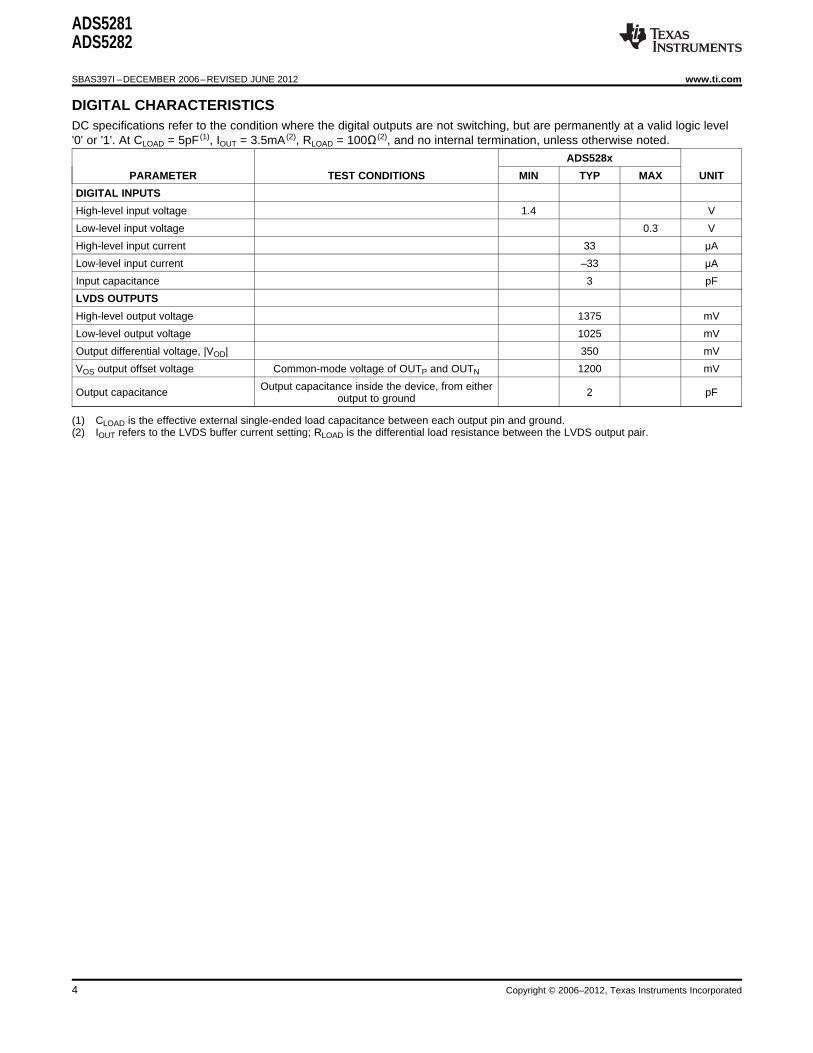
ADS5281ADS5282
SBAS397I ndashDECEMBER 2006ndashREVISED JUNE 2012 wwwticom
DIGITAL CHARACTERISTICSDC specifications refer to the condition where the digital outputs are not switching but are permanently at a valid logic level0 or 1 At CLOAD = 5pF (1) IOUT = 35mA (2) RLOAD = 100Ω (2) and no internal termination unless otherwise noted
ADS528x
PARAMETER TEST CONDITIONS MIN TYP MAX UNIT
DIGITAL INPUTS
High-level input voltage 14 V
Low-level input voltage 03 V
High-level input current 33 μA
Low-level input current ndash33 μA
Input capacitance 3 pF
LVDS OUTPUTS
High-level output voltage 1375 mV
Low-level output voltage 1025 mV
Output differential voltage |VOD| 350 mV
VOS output offset voltage Common-mode voltage of OUTP and OUTN 1200 mV
Output capacitance inside the device from eitherOutput capacitance 2 pFoutput to ground
(1) CLOAD is the effective external single-ended load capacitance between each output pin and ground(2) IOUT refers to the LVDS buffer current setting RLOAD is the differential load resistance between the LVDS output pair
4 Copyright copy 2006ndash2012 Texas Instruments Incorporated
ADS5281ADS5282
wwwticom SBAS397I ndashDECEMBER 2006ndashREVISED JUNE 2012
ELECTRICAL CHARACTERISTICS (1)
Typical values at +25degC Minimum and maximum values are measured across the specified temperature range of TMIN =ndash40degC to TMAX = +85degC AVDD = 33V LVDD = 18V clock frequency = 10MSPS to 65MSPS 50 clock duty cycle ndash1dBFSdifferential analog input internal reference mode ISET resistor = 562kΩ and LVDS buffer current setting = 35mA unlessotherwise noted
ADS528x
PARAMETER TEST CONDITIONS MIN TYP MAX UNIT
INTERNAL REFERENCE VOLTAGES
VREFB Reference bottom 05 V
VREFT Reference top 25 V
VREFT ndash VREFB 195 20 205 V
VCM Common-mode voltage (internal) 1425 15 1575 V
VCM output current plusmn2 mA
EXTERNAL REFERENCE VOLTAGES
VREFB Reference bottom 04 05 06 V
VREFT Reference top 24 25 26 V
VREFT ndash VREFB 19 20 21 V
ANALOG INPUT
Differential input voltage range 20 VPP
Differential input capacitance 3 pF
Analog input bandwidth 520 MHz
Analog input common-mode range DC-coupled input VCM plusmn 005 V
Per input pin per MSPS of sampling μAMHzAnalog input common-mode current 25speed per pin
Recovery from 6dB overload to within 1Voltage overload recovery time 1 Clock cycleaccuracy
Standard deviation seen on a periodicVoltage overload recovery repeatability first data within full-scale range in a 6dB 1 LSB
overloaded sine wave
DC ACCURACY
Offset error ndash125 plusmn02 +125 FS
Offset error temperature coefficient (2) plusmn5 ppmdegC
Channel gain error Excludes error in internal reference ndash08 FS
Channel gain error temperature Excludes temperature coefficient of plusmn10 ppmdegCcoefficient internal reference
Internal reference error temperature plusmn15 ppmdegCcoefficient (3)
DC PSRR DC power-supply rejection ratio (4) 15 mVV
POWER-DOWN MODES
Power in complete power-down mode 45 mW
Power in partial power-down mode Clock at 65MSPS 135 mW
Power with no clock 88 mW
DYNAMIC PERFORMANCE
5MHz full-scale signal applied to sevenCrosstalk channels measurement taken on channel ndash90 dBc
with no input signal
Two-tone third-order intermodulation f1 = 95MHz at ndash7dBFs ndash92 dBFSdistortion f2 = 102MHz at ndash7dBFs
(1) All characteristics are common for the ADS528x family(2) The offset temperature coefficient in ppmdegC is defined as (O1 ndash O2) times 106(T1 ndash T2)4096 where O1 and O2 are the offset codes in LSB
at the two extreme temperatures T1 and T2(3) The internal reference temperature coefficient is defined as (REF1 ndash REF2) times 106(T1 ndash T2)2 where REF1 and REF2 are the internal
reference voltages (VREFT ndash VREFB) at the two extreme temperatures T1 and T2(4) DC PSRR is defined as the ratio of the change in the ADC output (expressed in mV) to the change in supply voltage (in volts)
Copyright copy 2006ndash2012 Texas Instruments Incorporated 5
ADS5281ADS5282
SBAS397I ndashDECEMBER 2006ndashREVISED JUNE 2012 wwwticom
ELECTRICAL CHARACTERISTICS (BY DEVICE) (1)
Typical values at +25degC Minimum and maximum values are measured across the specified temperature range of TMIN =ndash40degC to TMAX = +85degC AVDD = 33V LVDD = 18V clock frequency = 10MSPS to 65MSPS 50 clock duty cycle ndash1dBFSdifferential analog input internal reference mode ISET resistor = 562kΩ and LVDS buffer current setting = 35mA unlessotherwise noted
ADS5281 ADS5281 ADS5282HTQFP-80 QFN-64 QFN-6450MSPS 50MSPS 65MSPS
PARAMETER TEST CONDITIONS MIN TYP MAX MIN TYP MAX MIN TYP MAX UNIT
DC ACCURACY
No missing codes Assured Assured Assured
DNL Differential nonlinearity ndash075 plusmn025 +075 ndash075 plusmn025 +075 ndash09 plusmn03 +09 LSB
INL Integral nonlinearity ndash15 plusmn07 +15 ndash15 plusmn07 +15 ndash17 plusmn07 +17 LSB
POWER SUPPLYmdashINTERNAL REFERENCE MODE
IAVDD Analog supply current 119 145 119 145 145 170 mA
ILVDD Digital current Zero input to all channels 76 95 76 95 89 102 mA
Total power 530 6495 530 6495 639 7446 mW
Obtained on powering down oneIncremental power saving 51 51 63 mW
channel at a time
POWER SUPPLYmdashEXTERNAL REFERENCE MODE
IAVDD Analog supply current 113 113 138 mA
ILVDD Digital current Zero input to all channels 76 76 89 mA
Total power 510 510 616 mW
Obtained on powering down oneIncremental power saving 50 50 61 mW
channel at a time
EXTERNAL REFERENCE LOADING
Current drawn by the eight ADCsfrom the external reference
Switching current 25 25 35 mAvoltages sourcing for REFT
sinking for REFB
DYNAMIC CHARACTERISTICS
fIN = 5MHz single-ended clock 74 85 74 85 72 85 dBcSFDR Spurious-free dynamic range
fIN = 30MHz differential clock 80 80 80 dBc
fIN = 5MHz single-ended clock 74 85 74 85 72 85 dBcHD2 Magnitude of second harmonic
fIN = 30MHz differential clock 82 82 82 dBc
fIN = 5MHz single-ended clock 74 85 74 85 72 85 dBcHD3 Magnitude of third harmonic
fIN = 30MHz differential clock 80 80 80 dBc
fIN = 5MHz single-ended clock 71 80 71 80 70 80THD Total harmonic distortion
fIN = 30MHz differential clock 78 78 78
fIN = 5MHz single-ended clock 683 70 683 70 683 70 dBFSSNR Signal-to-noise ratio
fIN = 30MHz differential clock 698 698 698 dBFS
fIN = 5MHz single-ended clock 677 697 677 697 673 697 dBFSSINAD Signal-to-noise and distortion
fIN = 30MHz differential clock 695 695 695 dBFS
(1) All characteristics are specific to each grade
6 Copyright copy 2006ndash2012 Texas Instruments Incorporated
60
59
58
57
56
55
54
53
52
51
50
49
48
47
46
45
44
43
42
41
AVDD
IN8N
IN8P
AVSS
IN7N
IN7P
AVDD
AVSS
IN6N
IN6P
AVSS
IN5N
IN5P
AVDD
LVSS
RESET
LVSS
LVSS
ADCLKN
ADCLKP
AV
SS
OU
T1
P
AV
SS
OU
T1
N
SC
LK
OU
T2
P
SD
ATA
OU
T2
N
CS
LV
DD
AV
DD
LV
SS
AV
SS
OU
T3
P
AV
SS
OU
T3
N
CLK
NO
UT
4P
CLK
PO
UT
4N
AV
DD
OU
T5
P
INT
EX
TO
UT
5N
AV
SS
OU
T6
P
RE
FT
OU
T6
N
RE
FB
LV
DD
VC
MLV
SS
I SE
TO
UT
7P
AV
DD
OU
T7
N
NC
OU
T8
P
TP
OU
T8
N
1
2
3
4
5
6
7
8
9
10
11
12
13
14
15
16
17
18
19
20
AVDD
IN1P
IN1N
AVSS
IN2P
IN2N
AVDD
AVSS
IN3P
IN3N
AVSS
IN4P
IN4N
AVDD
LVSS
PD
LVSS
LVSS
LCLKP
LCLKN
80 79 78 77 76 75 74 73 72 71 70
21 22 23 24 25 26 27 28 29 30 31
69
32 33 34 35 36 37 38 39 40
68 67 66 65 64 63 62 61
ADS528x
ADS5281ADS5282
wwwticom SBAS397I ndashDECEMBER 2006ndashREVISED JUNE 2012
PIN CONFIGURATIONS
TQFP-80TOP VIEW
Table 2 PIN DESCRIPTIONS TQFP-80
PIN NAME DESCRIPTION PIN NUMBER OF PINS
ADCLKN LVDS frame clock (1X)mdashnegative output 42 1
ADCLKP LVDS frame clock (1X)mdashpositive output 41 1
AVDD Analog power supply 33V 1 7 14 47 54 60 63 70 75 9
AVSS Analog ground 4 8 11 50 53 57 68 73 74 79 80 11
Negative differential clockCLKN 72 1Tie CLKN to 0V for a single-ended clock
CLKP Positive differential clock 71 1
CS Serial enable chip selectmdashactive low digital input 76 1
IN1N Negative differential input signal channel 1 3 1
IN1P Positive differential input signal channel 1 2 1
IN2N Negative differential input signal channel 2 6 1
Copyright copy 2006ndash2012 Texas Instruments Incorporated 7
ADS5281ADS5282
SBAS397I ndashDECEMBER 2006ndashREVISED JUNE 2012 wwwticom
Table 2 PIN DESCRIPTIONS TQFP-80 (continued)
PIN NAME DESCRIPTION PIN NUMBER OF PINS
IN2P Positive differential input signal channel 2 5 1
IN3N Negative differential input signal channel 3 10 1
IN3P Positive differential input signal channel 3 9 1
IN4N Negative differential input signal channel 4 13 1
IN4P Positive differential input signal channel 4 12 1
IN5N Negative differential input signal channel 5 49 1
IN5P Positive differential input signal channel 5 48 1
IN6N Negative differential input signal channel 6 52 1
IN6P Positive differential input signal channel 6 51 1
IN7N Negative differential input signal channel 7 56 1
IN7P Positive differential input signal channel 7 55 1
IN8N Negative differential input signal channel 8 59 1
IN8P Positive differential input signal channel 8 58 1
INTEXT Internalexternal reference mode select input 69 1
ISET Bias pinmdash562kΩ to ground 64 1
LCLKN LVDS bit clock (6X)mdashnegative output 20 1
LCLKP LVDS bit clock (6X)mdashpositive output 19 1
LVDD Digital and IO power supply 18V 25 35 2
LVSS Digital ground 15 17 18 26 36 43 44 46 8
NC No connection (or connect to ground) 62 1
OUT1N LVDS channel 1mdashnegative output 22 1
OUT1P LVDS channel 1mdashpositive output 21 1
OUT2N LVDS channel 2mdashnegative output 24 1
OUT2P LVDS channel 2mdashpositive output 23 1
OUT3N LVDS channel 3mdashnegative output 28 1
OUT3P LVDS channel 3mdashpositive output 27 1
OUT4N LVDS channel 4mdashnegative output 30 1
OUT4P LVDS channel 4mdashpositive output 29 1
OUT5N LVDS channel 5mdashnegative output 32 1
OUT5P LVDS channel 5mdashpositive output 31 1
OUT6N LVDS channel 6mdashnegative output 34 1
OUT6P LVDS channel 6mdashpositive output 33 1
OUT7N LVDS channel 7mdashnegative output 38 1
OUT7P LVDS channel 7mdashpositive output 37 1
OUT8N LVDS channel 8mdashnegative output 40 1
OUT8P LVDS channel 8mdashpositive output 39 1
PD Power-down input 16 1
REFB Negative reference inputoutput 66 1
REFT Positive reference inputoutput 67 1
RESET Active low RESET input 45 1
SCLK Serial clock input 78 1
SDATA Serial data input 77 1
TP Test pin do not use 61 1
VCM Common-mode output pin 15V output 65 1
8 Copyright copy 2006ndash2012 Texas Instruments Incorporated
48
47
46
45
44
43
42
41
40
39
38
37
36
35
34
33
IN8N
IN8P
AVSS
IN7N
IN7P
AVSS
IN6N
IN6P
AVSS
IN5N
IN5P
AVSS
LVSS
LVDD
OUT8N
OUT8P
1
2
3
4
5
6
7
8
9
10
11
12
13
14
15
16
IN1P
IN1N
AVSS
IN2P
IN2N
AVSS
IN3P
IN3N
AVSS
IN4P
IN4N
LVSS
PD
LVSS
OUT1P
OUT1N
RE
SE
T
SC
LK
SD
ATA
CS
AV
DD
CLK
N
CLK
P
AV
DD
INT
EX
T
RE
FT
RE
FB
VC
M
TP
I SE
T
AV
DD
AV
DD
OU
T2
P
OU
T2
N
OU
T3
P
OU
T3
N
OU
T4
P
OU
T4
N
AD
CLK
P
AD
CLK
N
LC
LK
P
LC
LK
N
OU
T5
P
OU
T5
N
OU
T6
P
OU
T6
N
OU
T7
P
OU
T7
N
64 63 62 61 60 59 58 57 56 55 54
17 18 19 20 21 22 23 24 25 26 27
53 52 51 50 49
28 29 30 31 32
ADS528X
ADS5281ADS5282
wwwticom SBAS397I ndashDECEMBER 2006ndashREVISED JUNE 2012
QFN-64 PowerPADTOP VIEW
Table 3 PIN DESCRIPTIONS QFN-64
PIN NAME DESCRIPTION PIN NUMBER OF PINS
ADCLKN LVDS frame clock (1X)mdashnegative output 24 1
ADCLKP LVDS frame clock (1X)mdashpositive output 23 1
AVDD Analog power supply 33V 49 50 57 60 4
AVSS Analog ground 3 6 9 37 40 43 46 7
Negative differential clock inputCLKN 59 1Tie CLKN to 0V for a single-ended clock
CLKP Positive differential clock input 58 1
CS Serial enable chip selectmdashactive low digital input 61 1
IN1N Negative differential input signal channel 1 2 1
IN1P Positive differential input signal channel 1 1 1
IN2N Negative differential input signal channel 2 5 1
IN2P Positive differential input signal channel 2 4 1
IN3N Negative differential input signal channel 3 8 1
IN3P Positive differential input signal channel 3 7 1
IN4N Negative differential input signal channel 4 11 1
IN4P Positive differential input signal channel 4 10 1
IN5N Negative differential input signal channel 5 39 1
Copyright copy 2006ndash2012 Texas Instruments Incorporated 9
ADS5281ADS5282
SBAS397I ndashDECEMBER 2006ndashREVISED JUNE 2012 wwwticom
Table 3 PIN DESCRIPTIONS QFN-64 (continued)
PIN NAME DESCRIPTION PIN NUMBER OF PINS
IN5P Positive differential input signal channel 5 38 1
IN6N Negative differential input signal channel 6 42 1
IN6P Positive differential input signal channel 6 41 1
IN7N Negative differential input signal channel 7 45 1
IN7P Positive differential input signal channel 7 44 1
IN8N Negative differential input signal channel 8 48 1
IN8P Positive differential input signal channel 8 47 1
INTEXT Internalexternal reference mode select input 56 1
ISET Bias pinmdash562kΩ to ground 51 1
LCLKN LVDS bit clock (6X)mdashnegative output 26 1
LCLKP LVDS bit clock (6X)mdashpositive output 25 1
LVDD Digital and IO power supply 18V 35 1
LVSS Digital ground 12 14 36 3
OUT1N LVDS channel 1mdashnegative output 16 1
OUT1P LVDS channel 1mdashpositive output 15 1
OUT2N LVDS channel 2mdashnegative output 18 1
OUT2P LVDS channel 2mdashpositive output 17 1
OUT3N LVDS channel 3mdashnegative output 20 1
OUT3P LVDS channel 3mdashpositive output 19 1
OUT4N LVDS channel 4mdashnegative output 22 1
OUT4P LVDS channel 4mdashpositive output 21 1
OUT5N LVDS channel 5mdashnegative output 28 1
OUT5P LVDS channel 5mdashpositive output 27 1
OUT6N LVDS channel 6mdashnegative output 30 1
OUT6P LVDS channel 6mdashpositive output 29 1
OUT7N LVDS channel 7mdashnegative output 32 1
OUT7P LVDS channel 7mdashpositive output 31 1
OUT8N LVDS channel 8mdashnegative output 34 1
OUT8P LVDS channel 8mdashpositive output 33 1
PD Power-down input 13 1
REFB Negative reference inputoutput 54 1
REFT Positive reference inputoutput 55 1
RESET Active low RESET input 64 1
SCLK Serial clock input 63 1
SDATA Serial data input 62 1
TP Test pin do not use 52 1
VCM Common-mode output pin 15V output 53 1
10 Copyright copy 2006ndash2012 Texas Instruments Incorporated
12-BitADC
PLL
Serializer
1x ADCLK
6x ADCLK
IN1P
IN1N
OUT1P
OUT1N
12-BitADC
SerializerIN2P
IN2N
OUT2P
OUT2N
12-BitADC
SerializerIN3P
IN3N
OUT3P
OUT3N
LCLKP
LCLKN
ADCLKP
ADCLKN
12x ADCLK
12-BitADC
SerializerIN4P
IN4N
OUT4P
OUT4N
12-BitADC
SerializerIN5P
IN5N
OUT5P
OUT5N
12-BitADC
SerializerIN6P
IN6N
OUT6P
OUT6N
12-BitADC
SerializerIN7P
IN7N
OUT7P
OUT7N
12-BitADC
Serializer
Digital
Digital
Digital
Digital
Digital
Digital
Digital
Digital
Reference
IN8P
IN8N
RE
FT
INT
EX
T
RE
FB
VC
M
OUT8P
OUT8N
I SE
T
Registers
SD
ATA
CS
RE
SE
T
SC
LK
ADC
Control
PD
Clock
Buffer
(AD
CL
K)
CL
KP
(AV
SS
)
CL
KN
AV
DD
(33
V)
LV
DD
(18
V)
Power-
Down
Te
st
Pa
tte
rns
Drive
Cu
rre
nt
Ou
tpu
t F
orm
at
Dig
ita
l G
ain
(0d
B-1
2d
B)
ADS5281ADS5282
wwwticom SBAS397I ndashDECEMBER 2006ndashREVISED JUNE 2012
FUNCTIONAL BLOCK DIAGRAM
Copyright copy 2006ndash2012 Texas Instruments Incorporated 11
tH1
tSU1
tH2
tSU2
LCLKN
LCLKP
OUTN
OUTP
D0 D1 D2 D3 D4 D5 D6 D7 D8 D9 D10 D11 D0 D1 D2 D3 D4 D5 D6 D7 D8 D9 D10 D11D0 D1 D2 D3 D4 D5 D6 D7 D8 D9 D10 D11
Sample nSample n + 12
tPROP
t (A)D
12 clocks latency
Analog Input
Clock Input
6X ADCLK
LCLKN
LCLKP
1X ADCLK
ADCLKN
ADCLKP
SERIAL DATA
OUTP
OUTN
tSAMPLE
Sample n + 13
ADS5281ADS5282
SBAS397I ndashDECEMBER 2006ndashREVISED JUNE 2012 wwwticom
LVDS TIMING DIAGRAM
DEFINITION OF SETUP AND HOLD TIMES
tSU = min(tSU1 tSU2)
tH = min(tH1 tH2)
TIMING CHARACTERISTICS (1) (2)
ADS528x
PARAMETER TEST CONDITIONS MIN TYP MAX UNIT
tA Aperture delay 15 45 ns
Aperture delay variation Channel-to-channel within the same device (3σ) plusmn20 ps
tJ Aperture jitter 400 fs
Time to valid data after coming out of 50 μsCOMPLETE POWER-DOWN mode
Time to valid data after coming out of PARTIALtWAKE Wake-up time POWER-DOWN mode (with clock continuing to 2 μs
run during power-down)
Time to valid data after stopping and restarting 40 μsthe input clock
ClockData latency 12 cycles
(1) Timing characteristics are common to the ADS528x family(2) Timing parameters are ensured by design and characterization not production tested
12 Copyright copy 2006ndash2012 Texas Instruments Incorporated
ADS5281ADS5282
wwwticom SBAS397I ndashDECEMBER 2006ndashREVISED JUNE 2012
LVDS OUTPUT TIMING CHARACTERISTICS (1) (2)
Typical values are at +25degC minimum and maximum values are measured across the specified temperature range of TMIN = ndash40degC to TMAX =+85degC sampling frequency = as specified CLOAD = 5pF (3) IOUT = 35mA RLOAD = 100Ω (4) and no internal termination unless otherwisenoted
ADS528x
40MSPS 50MSPS 65MSPS
PARAMETER TEST CONDITIONS (5) MIN TYP MAX MIN TYP MAX MIN TYP MAX UNIT
Data valid (7) to zero-crossing oftSU Data setup time(6) 067 047 027 ns
LCLKP
Zero-crossing of LCLKP to datatH Data hold time(6) 085 065 04 ns
becoming invalid(7)
Input clock (ADCLK) rising edgetPROP Clock propagation delay cross-over to output clock (ADCLKP) 10 14 166 10 125 141 97 115 14 ns
rising edge cross-over
Duty cycle of differential clockLVDS bit clock duty cycle 455 50 53 45 50 535 41 50 57
(LCLKP ndash LCLKN)
Bit clock cycle-to-cycle250 250 250 ps pp
jitter
Frame clock cycle-to-cycle150 150 150 ps pp
jitter
tRISE Data rise time data fall Rise time is from ndash100mV to +100mV009 02 04 009 02 04 009 02 04 ns
tFALL time Fall time is from +100mV to ndash100mV
tCLKRISE Output clock rise time Rise time is from ndash100mV to +100mV009 02 04 009 02 04 009 02 04 ns
tCLKFALL output clock fall time Fall time is from +100mV to ndash100mV
(1) All characteristics are at the maximum rated speed for each speed grade(2) Timing parameters are ensured by design and characterization not production tested(3) CLOAD is the effective external single-ended load capacitance between each output pin and ground(4) IOUT refers to the LVDS buffer current setting RLOAD is the differential load resistance between the LVDS output pair(5) Measurements are done with a transmission line of 100Ω characteristic impedance between the device and the load(6) Setup and hold time specifications take into account the effect of jitter on the output data and clock These specifications also assume
that data and clock paths are perfectly matched within the receiver Any mismatch in these paths within the receiver would appear asreduced timing margin
(7) Data valid refers to a logic high of +100mV and a logic low of ndash100mV
LVDS OUTPUT TIMING CHARACTERISTICS (1) (2)
Typical values are at +25degC minimum and maximum values are measured across the specified temperature range of TMIN = ndash40degC to TMAX =+85degC sampling frequency = as specified CLOAD = 5pF (3) IOUT = 35mA RLOAD = 100Ω (4) and no internal termination unless otherwisenoted
ADS528x
30MSPS 20MSPS 10MSPS
PARAMETER TEST CONDITIONS (5) MIN TYP MAX MIN TYP MAX MIN TYP MAX UNIT
Data valid (7) to zero-crossing oftSU Data setup time(6) 08 15 37 ns
LCLKP
Zero-crossing of LCLKP to datatH Data hold time(6) 12 19 39 ns
becoming invalid(7)
Input clock (ADCLK) rising edgetPROP Clock propagation delay cross-over to output clock (ADCLKP) 95 135 173 95 145 173 10 147 171 ns
rising edge cross-over
Duty cycle of differential clockLVDS bit clock duty cycle 465 50 52 48 50 51 49 50 51
(LCLKP ndash LCLKN)
Bit clock cycle-to-cycle250 250 750 ps pp
jitter
Frame clock cycle-to-cycle150 150 500 ps pp
jitter
tRISE Data rise time data fall Rise time is from ndash100mV to +100mV009 02 04 009 02 04 009 02 04 ns
tFALL time Fall time is from +100mV to ndash100mV
tCLKRISE Output clock rise time Rise time is from ndash100mV to +100mV009 02 04 009 02 04 009 02 04 ns
tCLKFALL output clock fall time Fall time is from +100mV to ndash100mV
(1) All characteristics are at the speeds other than the maximum rated speed for each speed grade(2) Timing parameters are ensured by design and characterization not production tested(3) CLOAD is the effective external single-ended load capacitance between each output pin and ground(4) IOUT refers to the LVDS buffer current setting RLOAD is the differential load resistance between the LVDS output pair(5) Measurements are done with a transmission line of 100Ω characteristic impedance between the device and the load(6) Setup and hold time specifications take into account the effect of jitter on the output data and clock These specifications also assume
that data and clock paths are perfectly matched within the receiver Any mismatch in these paths within the receiver would appear asreduced timing margin
(7) Data valid refers to a logic high of +100mV and a logic low of ndash100mV
Copyright copy 2006ndash2012 Texas Instruments Incorporated 13
t1
t2
t3
AVDD (3V to 36V)
LVDD (17V to 19V)
High-Level RESET
(14V to 36V)
High-Level CS
(14V to 36V)
Device Ready for
Serial Register Write(2)
Device Ready for
Data ConversionStart of Clock
AVDD
LVDD
RESET
CS
ADCLK
t4 t7
t5
t8
t6
ADS5281ADS5282
SBAS397I ndashDECEMBER 2006ndashREVISED JUNE 2012 wwwticom
LVDS OUTPUT TIMING CHARACTERISTICSTIMINGS WHEN USING REGISTER 0xE3 (2)
At 40 MSPSPARAMETER (1) TEST CONDITIONS
MIN TYP MAX
Data setup time Data valid (3) to zero-crossing of LCLKp 060
Data hold time Zero-crossing of LCLKP to data becoming invalid(3) 092
Input clock (ADCLK) rising edge cross-over to output clock (ADCLK) rising edgeClock propagation delay 8 12 146
crossover
(1) Only the setup time hold time and clock propagation delay parameters are affected Rest of the parameters are same as given inprevious two tables
(2) Only timing specifications for 40MSPS are affected when using register 0xE3 (as specified in the recommended operating table section)The timing specifications for other clock frequencies are same as given in previous two tables
(3) Data valid refers to logic high of +100mV and logic low of ndash100mV
RECOMMENDED POWER-UP SEQUENCING AND RESET TIMING
10μs lt t1 lt 50ms 10μs lt t2 lt 50ms ndash10ms lt t3 lt 10ms t4 gt 10ms t5 gt 100ns t6 gt 100ns t7 gt 10ms and t8 gt 100μs
(1) The AVDD and LVDD power on sequence does not matter as long as ndash10ms lt t3 lt 10ms Similar considerations apply while shuttingdown the device
(2) Write initialization registers listed in the Initialization Registers table
14 Copyright copy 2006ndash2012 Texas Instruments Incorporated
PD
Device Fully
Powers DownDevice Fully
Powers Up
tWAKE1 sm
ADS5281ADS5282
wwwticom SBAS397I ndashDECEMBER 2006ndashREVISED JUNE 2012
POWER-DOWN TIMING
Power-up time shown is based on 1μF bypass capacitors on the reference pins tWAKE is the time it takes for the device to wake upcompletely from power-down mode The ADS528x has two power-down modes complete power-down mode and partial power-down modeThe device can be configured in partial power-down mode through a register setting
tWAKE lt 50μs for complete power-down mode
tWAKE lt 2μs for partial power-down mode (provided the clock is not shut off during power-down)
Copyright copy 2006ndash2012 Texas Instruments Incorporated 15
D15 D14 D13 D12 D11 D10 D9 D8 D7 D6 D5 D4 D3 D2 D1 D0A7 A6 A5 A4 A3 A2 A1 A0
CS
SCLK
SDATA
Data latched on rising edge of SCLK
Start Sequence End Sequence
t6
t4
t2
t7
t3
t5
t1
ADS5281ADS5282
SBAS397I ndashDECEMBER 2006ndashREVISED JUNE 2012 wwwticom
SERIAL INTERFACE
The ADS528x has a set of internal registers that can be accessed through the serial interface formed by pins CS(chip select active low) SCLK (serial interface clock) and SDATA (serial interface data) When CS is low thefollowing actions occurbull Serial shift of bits into the device is enabledbull SDATA (serial data) is latched at every rising edge of SCLKbull SDATA is loaded into the register at every 24th SCLK rising edge
If the word length exceeds a multiple of 24 bits the excess bits are ignored Data can be loaded in multiples of24-bit words within a single active CS pulse The first eight bits form the register address and the remaining 16bits form the register data The interface can work with SCLK frequencies from 20MHz down to very low speeds(a few hertz) and also with a non-50 SCLK duty cycle
Register Initialization
After power-up the internal registers must be initialized to the respective default values Initialization can bedone in one of two ways1 Through a hardware reset by applying a low-going pulse on the RESET pin or2 Through a software reset using the serial interface set the RST bit high Setting this bit initializes the
internal registers to the respective default values and then self-resets the RST bit low In this case theRESET pin stays high (inactive)
After all registers have been initialized to their default values through a RESET operation the registers detailedin the Initialization Registers table must be written into This process must be done after every hardware orsoftware RESET operation in order to reconfigure the device for the best mode of operation
SERIAL INTERFACE TIMING
ADS528x
PARAMETER DESCRIPTION MIN TYP MAX UNIT
t1 SCLK period 50 ns
t2 SCLK high time 20 ns
t3 SCLK low time 20 ns
t4 Data setup time 5 ns
t5 Data hold time 5 ns
t6 CS fall to SCLK rise 8 ns
t7 Time between last SCLK rising edge to CS rising edge 8 ns
16 Copyright copy 2006ndash2012 Texas Instruments Incorporated
ADS5281ADS5282
wwwticom SBAS397I ndashDECEMBER 2006ndashREVISED JUNE 2012
SERIAL REGISTER MAP
Table 4 SUMMARY OF FUNCTIONS SUPPORTED BY SERIAL INTERFACE (1) (2) (3) (4)
ADDRESSIN HEX D15 D14 D13 D12 D11 D10 D9 D8 D7 D6 D5 D4 D3 D2 D1 D0 NAME DESCRIPTION DEFAULT
00 X RST Self-clearing software RESET Inactive
Channel-specific ADC power-X X X X X X X X PDN_CHlt81gt Inactive
down mode
Partial power-down mode (fastX PDN_PARTIAL Inactive
recovery from power-down)0F
Register mode for completeX PDN_COMPLETE Inactive
power-down (slower recovery)
Configures the PD pin for partial CompleteX PDN_PIN_CFG
power-down mode power-down
LVDS current driveX X X ILVDS_LCLKlt20gt programmability for LCLKN and 35mA drive
LCLKP pins
LVDS current driveILVDS_FRAME
11 X X X programmability for ADCLKN and 35mA drivelt20gt
ADCLKP pins
LVDS current driveX X X ILVDS_DATlt20gt programmability for OUTN and 35mA drive
OUTP pins
Enables internal termination for TerminationX EN_LVDS_TERM
LVDS buffers disabled
Programmable termination for Termination1 X X X TERM_LCLKlt20gt
LCLKN and LCLKP buffers disabled12
TERM_FRAME Programmable termination for Termination1 X X X
lt20gt ADCLKN and ADCLKP buffers disabled
Programmable termination for Termination1 X X X TERM_DATlt20gt
OUTN and OUTP buffers disabled
Channel-specific low-frequency14 X X X X X X X X LFNS_CHlt81gt Inactive
noise suppression mode enable
INP isSwaps the polarity of the analog
24 X X X X X X X X INVERT_CHlt81gt positiveinput pins electrically
input
Enables a repeating full-scaleX 0 0 EN_RAMP Inactive
ramp pattern on the outputs
Enables the mode wherein theDUALCUSTOM_
0 X 0 output toggles between two InactivePAT
defined codes
Enables the mode wherein theSINGLE_CUSTOM
0 0 X output is a constant specified Inactive25 _PAT
code
2MSBs for a single customBITS_CUSTOM1 pattern (and for the first code of
X X Inactivelt1110gt the dual custom pattern) lt11gt is
the MSB
BITS_CUSTOM2 2MSBs for the second code ofX X Inactive
lt1110gt the dual custom pattern
10 lower bits for the singleBITS_CUSTOM1 custom pattern (and for the first
26 X X X X X X X X X X Inactivelt90gt code of the dual custom pattern)
lt0gt is the LSB
BITS_CUSTOM2 10 lower bits for the second27 X X X X X X X X X X Inactive
lt90gt code of the dual custom pattern
X X X X GAIN_CH1lt30gt Programmable gain channel 1 0dB gain
X X X X GAIN_CH2lt30gt Programmable gain channel 2 0dB gain2A
X X X X GAIN_CH3lt30gt Programmable gain channel 3 0dB gain
X X X X GAIN_CH4lt30gt Programmable gain channel 4 0dB gain
X X X X GAIN_CH5lt30gt Programmable gain channel 5 0dB gain
X X X X GAIN_CH6lt30gt Programmable gain channel 6 0dB gain2B
X X X X GAIN_CH7lt30gt Programmable gain channel 7 0dB gain
X X X X GAIN_CH8lt30gt Programmable gain channel 8 0dB gain
(1) The unused bits in each register (identified as blank table cells) must be programmed as 0(2) X = Register bit referenced by the corresponding name and description (default is 0)(3) Bits marked as 0 should be forced to 0 and bits marked as 1 should be forced to 1 when the particular register is programmed(4) Multiple functions in a register should be programmed in a single write operation
Copyright copy 2006ndash2012 Texas Instruments Incorporated 17
ADS5281ADS5282
SBAS397I ndashDECEMBER 2006ndashREVISED JUNE 2012 wwwticom
Table 4 SUMMARY OF FUNCTIONS SUPPORTED BY SERIAL INTERFACE(1) (2) (3) (4) (continued)ADDRESS
IN HEX D15 D14 D13 D12 D11 D10 D9 D8 D7 D6 D5 D4 D3 D2 D1 D0 NAME DESCRIPTION DEFAULT
Single-1 X DIFF_CLK Differential clock mode
ended clock
Enables the duty-cycle correction1 X EN_DCC Disabled
circuit
External42Drives the external reference reference
1 X EXT_REF_VCMmode through the VCM pin drives REFT
and REFB
Controls the phase of LCLK1 X X PHASE_DDRlt10gt 90 degrees
output relative to data
0 X PAT_DESKEW Enables deskew pattern mode Inactive45
X 0 PAT_SYNC Enables sync pattern mode Inactive
Binary twos complement format Straight1 1 X BTC_MODE
for ADC output offset binary
Serialized ADC output comes LSB-first1 1 X MSB_FIRST
out MSB-first output
Enables SDR output modeDDR output46 1 1 X EN_SDR (LCLK becomes a 12x input
modeclock)
Controls whether the LCLK rising Rising edgeor falling edge comes in the of LCLK in
1 X 1 1 FALL_SDRmiddle of the data window when middle ofoperating in SDR output mode data window
SUMMARY OF FEATURES
POWER IMPACT (relative to default)FEATURES DEFAULT SELECTION AT fS = 65MSPS
ANALOG FEATURES
Internal or external reference Internal reference mode uses approximately 23mW moreNA Pin(driven on the REFT and REFB pins) power on AVDD
External reference driven on the Off Register 42 Approximately 9mW less power on AVDDVCM pin
Duty cycle correction circuit Off Register 42 Approximately 7mW more power on AVDD
With zero input to the ADC low-frequency noise suppressionLow-frequency noise suppression Off Register 14 causes digital switching at fS2 thereby increasing LVDD
power by approximately 7mWchannel
Differential clock mode uses approximately 7mW more powerSingle-ended or differential clock Single-ended Register 42 on AVDD
Refer to the Power-Down Modes section in the ElectricalPower-down mode Off Pin and register 0F Characteristics table
DIGITAL FEATURES
Programmable digital gain (0dB to Registers 2A and0dB No difference12dB) 2B
Straight offset or BTC output Straight offset Register 46 No difference
Swap polarity of analog input pins Off Register 24 No difference
LVDS OUTPUT PHYSICAL LAYER
LVDS internal termination Off Register 12 Approximately 7mW more power on AVDD
LVDS current programmability 35mA Register 11 As per LVDS clock and data buffer current setting
LVDS OUTPUT TIMING
LSB- or MSB-first output LSB-first Register 46 No difference
SDR mode uses approximately 2mW more power on LVDDDDR or SDR output DDR Register 46 (at fS = 30MSPS)
Refer toLCLK phase relative to data output Register 42 No differenceFigure 1
18 Copyright copy 2006ndash2012 Texas Instruments Incorporated
ADS5281ADS5282
wwwticom SBAS397I ndashDECEMBER 2006ndashREVISED JUNE 2012
DESCRIPTION OF SERIAL REGISTERS
SOFTWARE RESET
ADDRESSIN HEX D15 D14 D13 D12 D11 D10 D9 D8 D7 D6 D5 D4 D3 D2 D1 D0 NAME
00 X RST
Software reset is applied when the RST bit is set to 1 setting this bit resets all internal registers and self-clearsto 0
POWER-DOWN MODES
ADDRESSIN HEX D15 D14 D13 D12 D11 D10 D9 D8 D7 D6 D5 D4 D3 D2 D1 D0 NAME
X X X X X X X X PDN_CHlt81gt
X PDN_PARTIAL0F
0 X PDN_COMPLETE
X 0 PDN_PIN_CFG
Each of the eight channels can be individually powered down PDN_CHltNgt controls the power-down mode forthe ADC channel ltNgt
In addition to channel-specific power-down the ADS528x also has two global power-down modesmdashpartialpower-down mode and complete power-down mode Partial power-down mode partially powers down the chiprecovery from this mode is much quicker provided that the clock has been running for at least 50μs beforeexiting this mode Complete power-down mode on the other hand completely powers down the chip andinvolves a much longer recovery time
In addition to programming the device for either of these two power-down modes (through either thePDN_PARTIAL or PDN_COMPLETE bits respectively) the PD pin itself can be configured as either a partialpower-down pin or a complete power-down pin control For example if PDN_PIN_CFG = 0 (default) when thePD pin is high the device enters complete power-down mode However if PDN_PIN_CFG = 1 when the PD pinis high the device enters partial power-down mode
LVDS DRIVE PROGRAMMABILITY
ADDRESSIN HEX D15 D14 D13 D12 D11 D10 D9 D8 D7 D6 D5 D4 D3 D2 D1 D0 NAME
X X X ILVDS_LCLKlt20gt
11 X X X ILVDS_FRAMElt20gt
X X X ILVDS_DATlt20gt
The LVDS drive strength of the bit clock (LCLKP or LCLKN) and the frame clock (ADCLKP or ADCLKN) can beindividually programmed The LVDS drive strengths of all the data outputs OUTP and OUTN can also beprogrammed to the same value
Copyright copy 2006ndash2012 Texas Instruments Incorporated 19
ADS5281ADS5282
SBAS397I ndashDECEMBER 2006ndashREVISED JUNE 2012 wwwticom
All three drive strengths (bit clock frame clock and data) are programmed using sets of three bits Table 5shows an example of how the drive strength of the bit clock is programmed (the method is similar for the frameclock and data drive strengths)
Table 5 Bit Clock Drive Strength (1)
ILVDS_LCLKlt2gt ILVDS_LCLKlt1gt ILVDS_LCLKlt0gt LVDS DRIVE STRENGTH FOR LCLKP AND LCLKN
0 0 0 35mA (default)
0 0 1 25mA
0 1 0 15mA
0 1 1 05mA
1 0 0 75mA
1 0 1 65mA
1 1 0 55mA
1 1 1 45mA
(1) Current settings lower than 15mA are not recommended
LVDS INTERNAL TERMINATION PROGRAMMABILITY
ADDRESSIN HEX D15 D14 D13 D12 D11 D10 D9 D8 D7 D6 D5 D4 D3 D2 D1 D0 NAME
X EN_LVDS_TERM
1 X X X TERM_LCLKlt20gt12
1 X X X TERM_FRAMElt20gt
1 X X X TERM_DATlt20gt
The LVDS buffers have high-impedance current sources driving the outputs When driving traces whosecharacteristic impedance is not perfectly matched with the termination impedance on the receiver side there maybe reflections back to the LVDS output pins of the ADS528x that cause degraded signal integrity By enabling aninternal termination (between the positive and negative outputs) for the LVDS buffers the signal integrity can besignificantly improved in such scenarios To set the internal termination mode the EN_LVDS_TERM bit shouldbe set to 1 Once this bit is set the internal termination values for the bit clock frame clock and data bufferscan be independently programmed using sets of three bits Table 6 shows an example of how the internaltermination of the LVDS buffer driving the bit clock is programmed (the method is similar for the frame clock anddata buffers) These termination values are only typical values and can vary by up to plusmn20 across temperatureand from device to device
Table 6 Bit Clock Internal Termination
INTERNAL TERMINATION BETWEENTERM_LCLKlt2gt TERM_LCLKlt1gt TERM_LCLKlt0gt LCLKP AND LCLKN IN Ω
0 0 0 None
0 0 1 260
0 1 0 150
0 1 1 94
1 0 0 125
1 0 1 80
1 1 0 66
1 1 1 55
20 Copyright copy 2006ndash2012 Texas Instruments Incorporated
ADS5281ADS5282
wwwticom SBAS397I ndashDECEMBER 2006ndashREVISED JUNE 2012
LOW-FREQUENCY NOISE SUPPRESSION MODE
ADDRESSIN HEX D15 D14 D13 D12 D11 D10 D9 D8 D7 D6 D5 D4 D3 D2 D1 D0 NAME
14 X X X X X X X X LFNS_CHlt81gt
The low-frequency noise suppression mode is specifically useful in applications where good noise performance isdesired in the frequency band of 0MHz to 1MHz (around dc) Setting this mode shifts the low-frequency noise ofthe ADS528x to approximately fS2 thereby moving the noise floor around dc to a much lower valueLFNS_CHlt81gt enables this mode individually for each channel
ANALOG INPUT INVERT
ADDRESSIN HEX D15 D14 D13 D12 D11 D10 D9 D8 D7 D6 D5 D4 D3 D2 D1 D0 NAME
24 X X X X X X X X INVERT_CHlt81gt
Normally the INP pin represents the positive analog input pin and INN represents the complementary negativeinput Setting the bits marked INVERT_CHlt81gt (individual control for each channel) causes the inputs to beswapped INN now represents the positive input and INP the negative input
LVDS TEST PATTERNS
ADDRESSIN HEX D15 D14 D13 D12 D11 D10 D9 D8 D7 D6 D5 D4 D3 D2 D1 D0 NAME
X 0 0 EN_RAMP
0 X 0 DUALCUSTOM_PAT
25 0 0 X SINGLE_CUSTOM_PAT
X X BITS_CUSTOM1lt1110gt
X X BITS_CUSTOM2lt1110gt
26 X X X X X X X X X X BITS_CUSTOM1lt90gt
27 X X X X X X X X X X BITS_CUSTOM2lt90gt
0 X PAT_DESKEW45
X 0 PAT_SYNC
The ADS528x can output a variety of test patterns on the LVDS outputs These test patterns replace the normalADC data output Setting EN_RAMP to 1 causes all the channels to output a repeating full-scale ramp patternThe ramp increments from zero code to full-scale code in steps of 1LSB every clock cycle After hitting the full-scale code it returns back to zero code and ramps again
The device can also be programmed to output a constant code by setting SINGLE_CUSTOM_PAT to 1 andprogramming the desired code in BITS_CUSTOM1lt110gt In this mode BITS_CUSTOM1lt110gt take the placeof the 12-bit ADC data at the output and are controlled by LSB-first and MSB-first modes in the same way asnormal ADC data are
The device may also be made to toggle between two consecutive codes by programming DUAL_CUSTOM_PATto 1 The two codes are represented by the contents of BITS_CUSTOM1lt110gt and BITS_CUSTOM2lt110gt
In addition to custom patterns the device may also be made to output two preset patterns1 Deskew patten Set using PAT_DESKEW this mode replaces the 12-bit ADC output Dlt110gt with the
010101010101 word2 Sync pattern Set using PAT_SYNC the normal ADC word is replaced by a fixed 111111000000 word
Note that only one of the above patterns should be active at any given instant
Copyright copy 2006ndash2012 Texas Instruments Incorporated 21
ADS5281ADS5282
SBAS397I ndashDECEMBER 2006ndashREVISED JUNE 2012 wwwticom
PROGRAMMABLE GAIN
ADDRESSIN HEX D15 D14 D13 D12 D11 D10 D9 D8 D7 D6 D5 D4 D3 D2 D1 D0 NAME
X X X X GAIN_CH1lt30gt
X X X X GAIN_CH2lt30gt2A
X X X X GAIN_CH3lt30gt
X X X X GAIN_CH4lt30gt
X X X X GAIN_CH5lt30gt
X X X X GAIN_CH6lt30gt2B
X X X X GAIN_CH7lt30gt
X X X X GAIN_CH8lt30gt
In applications where the full-scale swing of the analog input signal is much less than the 2VPP range supportedby the ADS528x a programmable gain can be set to achieve the full-scale output code even with a lower analoginput swing The programmable gain not only fills the output code range of the ADC but also enhances the SNRof the device by utilizing quantization information from some extra internal bits The programmable gain for eachchannel can be individually set using a set of four bits indicated as GAIN_CHNlt30gt for Channel N The gainsetting is coded in binary from 0dB to 12dB as shown in Table 7
Table 7 Gain Setting for Channel 1
GAIN_CH1lt3gt GAIN_CH1lt2gt GAIN_CH1lt1gt GAIN_CH1lt0gt CHANNEL 1 GAIN SETTING
0 0 0 0 0dB
0 0 0 1 1dB
0 0 1 0 2dB
0 0 1 1 3dB
0 1 0 0 4dB
0 1 0 1 5dB
0 1 1 0 6dB
0 1 1 1 7dB
1 0 0 0 8dB
1 0 0 1 9dB
1 0 1 0 10dB
1 0 1 1 11dB
1 1 0 0 12dB
1 1 0 1 Do not use
1 1 1 0 Do not use
1 1 1 1 Do not use
22 Copyright copy 2006ndash2012 Texas Instruments Incorporated
VREF = 15V -B
VCM
15V
VREF = 15V +T
VCM
15V
ADS5281ADS5282
wwwticom SBAS397I ndashDECEMBER 2006ndashREVISED JUNE 2012
CLOCK REFERENCE AND DATA OUTPUT MODES
ADDRESSIN HEX D15 D14 D13 D12 D11 D10 D9 D8 D7 D6 D5 D4 D3 D2 D1 D0 NAME
1 X DIFF_CLK
1 X EN_DCC42
1 X EXT_REF_VCM
1 X X PHASE_DDRlt10gt
1 1 X BTC_MODE
1 1 X MSB_FIRST46
1 1 X EN_SDR
1 X 1 1 FALL_SDR
INPUT CLOCK
The ADS528x is configured by default to operate with a single-ended input clockmdashCLKP is driven by a CMOSclock and CLKN is tied to 0 However by programming DIFF_CLK to 1 the device can be made to work with adifferential input clock on CLKP and CLKN Operating with a low-jitter differential clock usually gives better SNRperformance especially at input frequencies greater than 30MHz
In cases where the duty cycle of the input clock falls outside the 45 to 55 range it is recommended to enablean internal duty cycle correction circuit This enabling is done by setting the EN_DCC bit to 1
EXTERNAL REFERENCE
The ADS528x can be made to operate in external reference mode by pulling the INTEXT pin to 0 In this modethe REFT and REFB pins should be driven with voltage levels of 25V and 05V respectively and must haveenough drive strength to drive the switched capacitance loading of the reference voltages by each ADC Theadvantage of using the external reference mode is that multiple ADS528x units can be made to operate with thesame external reference thereby improving parameters such as gain matching across devices However inapplications that do not have an available high drive differential external reference the ADS528x can still bedriven with a single external reference voltage on the VCM pin When EXT_REF_VCM is set as 1 (and theINTEXT pin is set to 0) the VCM pin is configured as an input pin and the voltages on REFT and REFB aregenerated as shown in Equation 1 and Equation 2
(1)
(2)
Copyright copy 2006ndash2012 Texas Instruments Incorporated 23
PHASE_DDRlt10gt = 00
PHASE_DDRlt10gt = 01
PHASE_DDRlt10gt = 10
PHASE_DDRlt10gt = 11
ADCLKP
LCLKP
OUTP
ADCLKP
LCLKP
OUTP
ADCLKP
LCLKP
OUTP
ADCLKP
LCLKP
OUTP
ADCLKP
LCLKP
OUTP
ADS5281ADS5282
SBAS397I ndashDECEMBER 2006ndashREVISED JUNE 2012 wwwticom
BIT CLOCK PROGRAMMABILITY
The output interface of the ADS528x is normally a DDR interface with the LCLK rising edge and falling edgetransitions in the middle of alternate data windows This default phase is shown in Figure 1
Figure 1 Default Phase of LCLK
The phase of LCLK can be programmed relative to the output frame clock and data using bitsPHASE_DDRlt10gt The LCLK phase modes are shown in Figure 2
Figure 2 Phase Programmability Modes for LCLK
24 Copyright copy 2006ndash2012 Texas Instruments Incorporated
EN_SDR = 1 FALL_SDR = 0
EN_SDR = 1 FALL_SDR = 1
ADCLKP
LCLKP
OUTP
ADCLKP
LCLKP
OUTP
ADS5281ADS5282
wwwticom SBAS397I ndashDECEMBER 2006ndashREVISED JUNE 2012
In addition to programming the phase of LCLK in the DDR mode the device can also be made to operate in SDRmode by setting the EN_SDR bit to 1 In this mode the bit clock (LCLK) is output at 12x times the input clock ortwice the rate as in DDR mode Depending on the state of FALL_SDR LCLK may be output in either of the twomanners shown in Figure 3 As can be seen in Figure 3 only the LCLK rising (or falling) edge is used to capturethe output data in SDR mode
Figure 3 SDR Interface Modes
The SDR mode does not work well beyond 40MSPS because the LCLK frequency becomes very high
DATA OUTPUT FORMAT MODES
The ADC output by default is in straight offset binary mode Programming the BTC_MODE bit to 1 inverts theMSB and the output becomes binary twos complement mode
Also by default the first bit of the frame (following the rising edge of ADCLKP) is the LSB of the ADC outputProgramming the MSB_FIRST mode inverts the bit order in the word and the MSB is output as the first bitfollowing the ADCLKP rising edge
Copyright copy 2006ndash2012 Texas Instruments Incorporated 25
0
-
-
-
-
-
-
-
-
-
20
40
60
80
100
120
140
160
180
Input Frequency (MHz)
0 25
Am
plit
ude (
dB
)
2015105
SFDR = 884dBc
SNR = 709dBFS
SINAD = 708dBFS
THD = 875dBc
0
-
-
-
-
-
-
-
-
-
20
40
60
80
100
120
140
160
180
Input Frequency (MHz)
0 25
Am
plit
ude (
dB
)
2015105
SFDR = 856dBc
SNR = 705dBFS
SINAD = 704dBFS
THD = 839dBc
0
-
-
-
-
-
-
-
-
-
20
40
60
80
100
120
140
160
180
Input Frequency (MHz)
0 2 20
Am
plit
ude (
dB
)
1816141210864
SFDR = 853dBc
SNR = 708dBFS
SINAD = 707dBFS
THD = 893dBc
0
-
-
-
-
-
-
-
-
-
20
40
60
80
100
120
140
160
180
Input Frequency (MHz)
0 2 20
Am
plit
ude (
dB
)
1816141210864
SFDR = 828dBc
SNR = 702dBFS
SINAD = 70dBFS
THD = 823dBc
ADS5281ADS5282
SBAS397I ndashDECEMBER 2006ndashREVISED JUNE 2012 wwwticom
TYPICAL CHARACTERISTICSAt TA = +25degC AVDD = +33V LVDD = 18V clock frequency = 65MSPS differential clock mode 1VPP clock amplitude 50
clock duty cycle input frequency = 10MHz ndash1dBFS differential analog input 0dB digital gain setting 15V analog inputcommon-mode low-frequency noise suppression = off internal reference mode ISET resistor = 562kΩ and LVDS buffer
current setting = 35mA unless otherwise noted
SPECTRAL PERFORMANCE SPECTRAL PERFORMANCE(fS = 40MHz fIN = 10MHz) (fS = 40MHz fIN = 25MHz)
Figure 4 Figure 5
SPECTRAL PERFORMANCE SPECTRAL PERFORMANCE(fS = 50MHz fIN = 10MHz) (fS = 50MHz fIN = 25MHz)
Figure 6 Figure 7
26 Copyright copy 2006ndash2012 Texas Instruments Incorporated
0
-20
-40
-60
-80
-100
-120
-140
-180
Input Frequency (MHz)
0 33
Am
plit
ude (
dB
)
2015105
-160
SFDR = 862dBc
SNR = 705dBFS
SNR (0MHz to 1MHz) = 861dBFS
SINAD = 704dBFS
THD = 854dBc
25 30
92
87
82
77
72
67
Input Frequency (MHz)
5 30
Dynam
ic P
erf
orm
ance (
SN
R S
FD
R)
201510 25
SNR (dBFS)
SFDR (dBc)
f = 40MHzS
0
-
-
-
-
-
-
-
-
-
20
40
60
80
100
120
140
160
180
Input Frequency (MHz)
0 33
Am
plit
ude (
dB
)
2015105 25 30
SFDR = 909dBc
SNR = 708dBFS
SINAD = 707dBFS
THD = 904dBc
0
-20
-40
-60
-80
-100
-120
-140
-180
Input Frequency (MHz)
0 33
Am
plit
ude (
dB
)
2015105
-160
SFDR = 874dBc
SNR = 704dBFS
SNR (0MHz to 1MHz) = 819dBFS
SINAD = 703dBFS
THD = 864dBc
25 30
ADS5281ADS5282
wwwticom SBAS397I ndashDECEMBER 2006ndashREVISED JUNE 2012
TYPICAL CHARACTERISTICS (continued)At TA = +25degC AVDD = +33V LVDD = 18V clock frequency = 65MSPS differential clock mode 1VPP clock amplitude 50clock duty cycle input frequency = 10MHz ndash1dBFS differential analog input 0dB digital gain setting 15V analog inputcommon-mode low-frequency noise suppression = off internal reference mode ISET resistor = 562kΩ and LVDS buffercurrent setting = 35mA unless otherwise noted
SPECTRAL PERFORMANCE SPECTRAL PERFORMANCE(fS = 65MHz fIN = 10MHz) (fS = 65MHz fIN = 25MHz)
Figure 8 Figure 9
SPECTRAL PERFORMANCE LOW-FREQUENCY NOISESUPPRESSION MODE ENABLED
(fS = 65MHz fIN = 25MHz) DYNAMIC PERFORMANCE vs INPUT FREQUENCY
Figure 10 Figure 11
Copyright copy 2006ndash2012 Texas Instruments Incorporated 27
95
85
75
65
55
45
35
25
Input Amplitude (dBFS)
Dyn
am
ic P
erf
orm
an
ce
(S
NR
S
FD
R)
SNR (dBFS)
SFDR (dBc)
f = 65MHz
f = 10MHzS
IN
-60 0-50 -40 -30 -20 -10
94
89
84
79
74
69
Clock Amplitude (V Differential)PP
06 23
Dynam
ic P
erf
orm
ance (
SN
R S
FD
R)
1611
SNR (dBFS)
SFDR (dBc)
f = 65MHz
f = 10MHzS
IN
21
95
90
85
80
75
70
65
60
Digital Gain (dB)
0 12
Dyn
am
ic P
erf
orm
an
ce
(S
NR
S
FD
R)
642 8
SNR (dBFS)
SFDR (dBc)
f = 65MHz
f = 10MHzS
IN
10
95
90
85
80
75
70
65
60
AVDD (V)
30 36
Dynam
ic P
erf
orm
ance (
SN
R S
FD
R)
333231 34
SNR (dBFS)
SFDR (dBc)
f = 65MHz
f = 10MHzS
IN
35
92
87
82
77
72
67
Input Frequency (MHz)
5 30
Dynam
ic P
erf
orm
ance (
SN
R S
FD
R)
201510 25
SNR (dBFS)
SFDR (dBc)
f = 50MHzS
97
92
87
82
77
72
67
Input Frequency (MHz)
5 30
Dynam
ic P
erf
orm
ance (
SN
R S
FD
R)
201510 25
SNR (dBFS)
SFDR (dBc)
f = 65MHzS
ADS5281ADS5282
SBAS397I ndashDECEMBER 2006ndashREVISED JUNE 2012 wwwticom
TYPICAL CHARACTERISTICS (continued)At TA = +25degC AVDD = +33V LVDD = 18V clock frequency = 65MSPS differential clock mode 1VPP clock amplitude 50clock duty cycle input frequency = 10MHz ndash1dBFS differential analog input 0dB digital gain setting 15V analog inputcommon-mode low-frequency noise suppression = off internal reference mode ISET resistor = 562kΩ and LVDS buffercurrent setting = 35mA unless otherwise noted
DYNAMIC PERFORMANCE vs INPUT FREQUENCY DYNAMIC PERFORMANCE vs INPUT FREQUENCY
Figure 12 Figure 13
DYNAMIC PERFORMANCE vs DIGITAL GAIN DYNAMIC PERFORMANCE vs AVDD
Figure 14 Figure 15
DYNAMIC PERFORMANCE vs INPUT AMPLITUDE DYNAMIC PERFORMANCE vs CLOCK AMPLITUDE
Figure 16 Figure 17
28 Copyright copy 2006ndash2012 Texas Instruments Incorporated
94
89
84
79
74
69
External Reference Common-Mode Voltage (REF + REF )2 (V)T B
135 165
Dynam
ic P
erf
orm
ance (
SN
R S
FD
R)
150145140
SNR (dBFS)
SFDR (dBc)
f = 65MHz
f = 10MHzS
IN
155 160
External reference differential voltage maintained at 2V
94
89
84
79
74
69
Voltage on V (V)CM
135 165
Dynam
ic P
erf
orm
ance (
SN
R S
FD
R)
150145140
SNR (dBFS)
SFDR (dBc)
f = 65MHz
f = 10MHzS
IN
155 160
94
89
84
79
74
69
Analog Input Common-Mode Voltage (V)
130 170
Dynam
ic P
erf
orm
ance (
SN
R S
FD
R)
140135
SNR (dBFS)
SFDR (dBc)
f = 65MHz
f = 10MHzS
IN
145 165160155150
94
89
84
79
74
69
External Reference Differential Voltage REF REF (V)-T B
16 24
Dynam
ic P
erf
orm
ance (
SN
R S
FD
R)
191817
SNR (dBFS)
SFDR (dBc)
f = 65MHz
f = 10MHzS
IN
20 232221
External reference common-mode voltage
maintained at 15V
ADS5281ADS5282
wwwticom SBAS397I ndashDECEMBER 2006ndashREVISED JUNE 2012
TYPICAL CHARACTERISTICS (continued)At TA = +25degC AVDD = +33V LVDD = 18V clock frequency = 65MSPS differential clock mode 1VPP clock amplitude 50clock duty cycle input frequency = 10MHz ndash1dBFS differential analog input 0dB digital gain setting 15V analog inputcommon-mode low-frequency noise suppression = off internal reference mode ISET resistor = 562kΩ and LVDS buffercurrent setting = 35mA unless otherwise noted
DYNAMIC PERFORMANCE vs ANALOG INPUT COMMON- DYNAMIC PERFORMANCE vs EXTERNAL REFERENCEMODE VOLTAGE DIFFERENTIAL VOLTAGE
Figure 18 Figure 19
DYNAMIC PERFORMANCE vs EXTERNAL REFERENCE DYNAMIC PERFORMANCE vs EXTERNAL REFERENCECOMMON-MODE VOLTAGE FORCED THROUGH VCM
Figure 20 Figure 21
Copyright copy 2006ndash2012 Texas Instruments Incorporated 29
05
04
03
02
01
0
-01
-02
-05
Code (LSB)
0 4096
INL
(L
SB
)
30722048 25601536 35841024512
-04
-03
f = 50MSPS
f = 5MHzS
IN
035
025
015
005
-005
-015
-035
Code (LSB)
0 4096
DN
L (
LS
B)
30722048 25601536 35841024512
-025
f = 50MSPS
f = 5MHzS
IN
60
50
40
30
20
10
0
Code Bin (LSB)
2049
Occurr
ence (
)
20532051 2054
f = 65MSPSS
2050 2052
0 0037 028
5192
4743
10
-10
-30
-50
-70
-90
-110
-130
-150
Input Frequency (MHz)
0 2 20
Am
plit
ude (
dB
)
1816141210864
f = 65MHz
f = 10MHz ( 7dBFS)
f = 161MHz ( 7dBFS)
IMD = 97dBFS
-
-
-
S
1
2
95
90
85
80
75
70
65
60
Clock Duty Cycle ()
35 65
Dynam
ic P
erf
orm
ance (
SN
R S
FD
R)
504540 55
SNR (dBFS)
SFDR (dBc)
f = 65MHz
f = 10MHzS
IN
60
95
85
80
75
70
60
Clock Duty Cycle ()
20 80
Dynam
ic P
erf
orm
ance (
SN
R S
FD
R)
504030 60
SNR (dBFS)
SFDR (dBc)
f = 65MHz
f = 10MHzS
IN
90
70
65
ADS5281ADS5282
SBAS397I ndashDECEMBER 2006ndashREVISED JUNE 2012 wwwticom
TYPICAL CHARACTERISTICS (continued)At TA = +25degC AVDD = +33V LVDD = 18V clock frequency = 65MSPS differential clock mode 1VPP clock amplitude 50clock duty cycle input frequency = 10MHz ndash1dBFS differential analog input 0dB digital gain setting 15V analog inputcommon-mode low-frequency noise suppression = off internal reference mode ISET resistor = 562kΩ and LVDS buffercurrent setting = 35mA unless otherwise noted
DYNAMIC PERFORMANCE vs CLOCK DUTY CYCLE DCC DYNAMIC PERFORMANCE vs CLOCK DUTY CYCLE DCCDISABLED ENABLED
Figure 22 Figure 23
HISTOGRAM OF OUTPUT CODE FOR ZERO INPUT INTERMODULATION DISTORTION
Figure 24 Figure 25
INTEGRAL NONLINEARITY DIFFERENTIAL NONLINEARITY
Figure 26 Figure 27
30 Copyright copy 2006ndash2012 Texas Instruments Incorporated
064
062
060
058
056
054
052
Sta
ndard
Devia
tion (
LS
B)
0 1 2 3 4 5 6
Overload Signal Amplitude (dBFS)
f = 65MSPS
f = 5MHzS
IN
Standard Deviation of
2nd Point After Overload
Standard Deviation of
1st Point After Overload
tS
16384 t (Group 1)S
Set 1 Point 1 (of 16) Set 1 Point 2 (of 16)
First point after overload (Set 1)
First point after overload (Set 2)
Second point after overload (Set 2)
Second point after overload (Set 1)
Overload
Amplitude
NOTES
Input sine wave phase is repetitive over 16384 clock cycles
16 such repetitive groups (of 16384 clock cycles) are capturedndasha total of 262144 points
Standard deviation of every set of are analyzed over the 16 groups
Worst case of all such standard deviations are plotted in the graphs
first and second points after overload
+FS
-FS
070
068
066
064
062
060
058
056
054
052
050
Sta
nd
ard
De
via
tio
n (
in L
SB
)
0 1 2 3 4 5 6
Overload Signal Amplitude (dBFS)
f = 50MSPS
f = 5MHzS
IN Standard Deviation of
2nd Point After Overload
Standard Deviation of
1st Point After Overload
170
130
110
90
70
30
Clock Frequency (MSPS)
5 75
I I
(mA
)A
VD
DLV
DD
352515 45
ILVDD
IAVDD
Zero Input on All Channels
Internal Reference Mode150
55
50
65
075
055
035
015
-005
-025
-065
Code (LSB)
0 4096
INL
(LS
B)
30722048 25601536 35841024512
-045
f = 65MSPS
f = 5MHzS
IN
035
025
015
005
-005
-015
-035
Code (LSB)
0 4096
DN
L (
LS
B)
30722048 25601536 35841024512
-025
f = 65MSPS f = 5MHzS IN
ADS5281ADS5282
wwwticom SBAS397I ndashDECEMBER 2006ndashREVISED JUNE 2012
TYPICAL CHARACTERISTICS (continued)At TA = +25degC AVDD = +33V LVDD = 18V clock frequency = 65MSPS differential clock mode 1VPP clock amplitude 50clock duty cycle input frequency = 10MHz ndash1dBFS differential analog input 0dB digital gain setting 15V analog inputcommon-mode low-frequency noise suppression = off internal reference mode ISET resistor = 562kΩ and LVDS buffercurrent setting = 35mA unless otherwise noted
INTEGRAL NONLINEARITY DIFFERENTIAL NONLINEARITY
Figure 28 Figure 29
AVDD AND LVDD POWER-SUPPLY CURRENTSvs CLOCK FREQUENCY OVERLOAD RECOVERY AT 50MSPS
Figure 30 Figure 31
OVERLOAD RECOVERY AT 65MSPS
Figure 32 Figure 33 Overload Recovery
Copyright copy 2006ndash2012 Texas Instruments Incorporated 31
ADS5281ADS5282
SBAS397I ndashDECEMBER 2006ndashREVISED JUNE 2012 wwwticom
APPLICATION INFORMATION
The ADC output goes to a serializer that operatesTHEORY OF OPERATION from a 12x clock generated by the PLL The 12 databits from each channel are serialized and sent LSBThe ADS528x devices are a family of 8-channelfirst In addition to serializing the data the serializerhigh-speed CMOS ADCs The 12 bits given out byalso generates a 1x clock and a 6x clock Theseeach channel are serialized and sent out on a singleclocks are generated in the same way the serializedpair of pins in LVDS format All eight channels of thedata are generated so these clocks maintain perfectADS528x operate from a single clock (ADCLK) Thesynchronization with the data The data and clocksampling clocks for each of the eight channels areoutputs of the serializer are buffered externally usinggenerated from the input clock using a carefullyLVDS buffers Using LVDS buffers to transmit datamatched clock buffer tree The 12x clock required forexternally has multiple advantages such as athe serializer is generated internally from ADCLKreduced number of output pins (saving routing spaceusing a phase-locked loop (PLL) A 6x and a 1x clockon the board) reduced power consumption andare also output in LVDS format along with the datareduced effects of digital noise coupling to the analogto enable easy data capture The ADS528x operatescircuit inside the ADS528xfrom internally-generated reference voltages that are
trimmed to improve to a high level of accuracy The ADS528x operates from two sets of supplies andTrimmed references improve the gain matching grounds The analog supply and ground set isacross devices and provide the option to operate the identified as AVDD and AVSS while the digital set isdevices without having to externally drive and route identified by LVDD and LVSSreference lines The nominal values of REFT andREFB are 25V and 05V respectively The ANALOG INPUTreferences are internally scaled down differentially bya factor of 2 This scaling results in a differential input The analog input consists of a switched-capacitorof ndash1V to correspond to the zero code of the ADC based differential sample-and-hold architecture Thisand a differential input of +1V to correspond to the differential topology results in very good acfull-scale code (4095 LSB) VCM (the common-mode performance even for high input frequencies at highvoltage of REFT and REFB) is also made available sampling rates The INN and INP pins must beexternally through a pin and is nominally 15V externally biased around a common-mode voltage of
15V available on VCM For a full-scale differentialThe ADC employs a pipelined converter architectureinput each input pin (INN and INP) must swingthat consists of a combination of multi-bit and single-symmetrically between VCM + 05V and VCM ndash 05Vbit internal stages Each stage feeds its data into theresulting in a 2VPP differential input swing Thedigital error correction logic ensuring excellentmaximum input peak-to-peak differential swing isdifferential linearity and no missing codes at the 12-determined to be the difference between the internalbit levelreference voltages REFT (25V nominal) and REFB(05V nominal) Figure 34 illustrates the model of theinput driving circuit
32 Copyright copy 2006ndash2012 Texas Instruments Incorporated
CM Buffer
Internal
Voltage
Reference
Input
Circuitry
INP
INN
VCM
12kW
12kW
ADS528x
(2mA) facute S
50MSPS
5nH to 9nH (TQFP-80)
2nH to 3nH (QFN-64)
15pF
to 24pF
IN OUT
INP
15pF to
25pF
1W
1000W
to 1440W
5W
to 10W
1000W
to 1440W
5nH to 9nH (TQFP-80)
2nH to 3nH (QFN-64)
INN
15pF to
25pF
1W
15W
to 25W
15W
to 30W
02pF
to 03pF
IN OUT
15pF
to 24pF
IN OUT
5W
to 10W
15W
to 25W
15W
to 30W
IN OUT
IN
OUT
16 to 32W W
IN OUT
IN OUT
OUTP
OUTN
Switches that are ON
in SAMPLE phase
Switches that are ON
in HOLD phase
ADS5281ADS5282
wwwticom SBAS397I ndashDECEMBER 2006ndashREVISED JUNE 2012
Figure 34 Analog Input Circuit Model
during ac-coupling by increasing VCM by roughlyInput Common-Mode Current 75mV When operating above 50MSPS it is
recommended that additional parallel resistors beThe input stage of all eight ADCs together sinks aadded externally to restore the input common-modecommon-mode current on the order of 2mA atto at least 14V if the inputs are to be ac-coupled50MSPS Equation 3 describes the dependency of
the common-mode current and the samplingfrequency
(3)
If the driving stage is dc-coupled to the inputs thenEquation 3 can be used to determine its common-mode drive capability and impedance The inputs canalso be ac-coupled to the INN and INP pins In thatcase the input common-mode is set by two internal12kΩ resistors connecting the input pins to VCM Thisarchitecture is shown in Figure 35
When the inputs are ac-coupled there is a drop inthe voltages at INP and INN relative to VCM This can Dashed area denotes one of eight channelsbe computed from Equation 3 At 50MSPS for
Figure 35 Common-Mode Biasing of Input Pinsexample the drop at each of the 16 input pins is150mV which is not optimal for ADC operationInitialization Registers 1 and 5 described in theInitialization Registers table can be used to partiallyreduce the effect of this input common-mode drop
Copyright copy 2006ndash2012 Texas Instruments Incorporated 33
01 Fm 50W
50W
200W
200W
INP
VCM
INN
01 Fm
12 21
47W
47W
01 Fm
01 Fm
25W
25W
11
INP
VCM
INN
ADS5281ADS5282
SBAS397I ndashDECEMBER 2006ndashREVISED JUNE 2012 wwwticom
Driving Circuit At high input frequencies the mismatch in thetransformer parasitic capacitance (between theFor optimum performance the analog inputs must bewindings) results in degraded even-order harmonicdriven differentially This approach improves theperformance Connecting two identical RFcommon-mode noise immunity and even-ordertransformers back-to-back helps to minimize thisharmonic rejection Input configurations using RFmismatch and good performance is obtained fortransformers suitable for low and high inputhigh-frequency input signals An additionalfrequencies are shown in Figure 36 and Figure 37termination resistor pair is required between the tworespectively The single-ended signal is fed to thetransformers as shown in Figure 37 The center pointprimary winding of the RF transformer Theof this termination is connected to ground to improvetransformer is terminated by 50Ω resistor on thethe balance between the positive and negative sidessecondary side Placing the termination on theThe values of the terminations between thesecondary side helps to shield the kicks caused bytransformers and on the secondary side must bethe input sampling capacitors from the RFchosen to achieve an overall 50Ω (in the case of 50Ωtransformer leakage inductances The termination issource impedance)accomplished by two 25Ω resistors connected in
series with the center point connected to the 15Vcommon-mode The 47Ω resistor in series with eachinput pin is required to damp the ringing caused bythe device package parasitics
Figure 36 Drive Circuit at Low Input Frequencies
Figure 37 Drive Circuit at High Input Frequencies
34 Copyright copy 2006ndash2012 Texas Instruments Incorporated
CLKP
CLKN
CMOS Clock Input
01 Fm
01 Fm
CLKP
CLKN
CMOS Single-Ended
Clock
0V
CLKP
CLKN
Differential Sine-Wave
PECL or LVDS Clock Input
01 Fm
01 Fm
5kW 5kW
VCM
CLKP
CLKN
VCM
ADS5281ADS5282
wwwticom SBAS397I ndashDECEMBER 2006ndashREVISED JUNE 2012
CLOCK INPUT
The eight channels on the device operate from asingle ADCLK input To ensure that the aperturedelay and jitter are the same for all channels a clocktree network is used to generate individual samplingclocks to each channel The clock paths for all thechannels are matched from the source point to thesampling circuit This architecture ensures that theperformance and timing for all channels are identicalThe use of the clock tree for matching introduces anaperture delay that is defined as the delay betweenthe rising edge of ADCLK and the actual instant ofsampling The aperture delays for all the channelsare matched to the best possible extent A mismatchof plusmn20ps (plusmn3σ) could exist between the apertureinstants of the eight ADCs within the same chip Figure 39 Internal Clock BufferHowever the aperture delays of ADCs across twodifferent chips can be several hundred picosecondsapart
The ADS528x can be made to operate either inCMOS single-ended clock mode (default isDIFF_CLK = 0) or differential clock mode (SINELVPECL or LVDS) When operating in the single-ended clock mode CLKN must be forced to 0VDCand the single-ended CMOS applied on the CLKP pinThis operation is shown in Figure 38
Figure 40 Differential Clock Driving Circuit(DIFF_CLK = 1)
Figure 38 Single-Ended Clock Driving Circuit(DIFF_CLK = 0)
When configured to operate in the differential clock Figure 41 Single-Ended Clock Driving Circuitmode (register bit DIFF_CLK = 1) the ADS528x clock When DIFF_CLK = 1inputs can be driven differentially (SINE LVPECL orLVDS) with little or no difference in performance
For best performance the clock inputs must bebetween them or with a single-ended (LVCMOS)driven differentially in order to reduce susceptibility toThe common-mode voltage of the clock inputs is setcommon-mode noise For high input frequencyto VCM using internal 5kΩ resistors as shown insampling it is recommended to use a clock sourceFigure 39 This method allows using transformer-with very low jitter Bandpass filtering of the clockcoupled drive circuits for a sine wave clock or ac-source can help reduce the effect of jitter If the dutycoupling for LVPECL and LVDS clock sources ascycle deviates from 50 by more than 2 or 3 it isshown in Figure 40 When operating in the differentialrecommended to enable the DCC through register bitclock mode the single-ended CMOS clock can be ac-EN_DCCcoupled to the CLKP input with CLKN (pin 11)
connected to ground with a 01μF capacitor asshown in Figure 41
Copyright copy 2006ndash2012 Texas Instruments Incorporated 35
Threshold 1 Threshold 2 Threshold 3
10 MHz 45 MHz 65 MHz
Sampling Frequency
ADS5281ADS5282
SBAS397I ndashDECEMBER 2006ndashREVISED JUNE 2012 wwwticom
PLL OPERATION ACROSS SAMPLING Step 2 Disable the PLL automatic switch and setFREQUENCY the PLL configuration depending on the clock
frequencyThe ADS528X uses a PLL for generating the highspeed bit clock (LCLK) the frame clock (ADCLK) amp SAMPLE CLOCK FREQUENCY REGISTER SETTING (Hex)internal clocks for the serializer operation RANGE (MSPS)
Min Max Address DataTo enable operation across the entire frequencyrange the PLL is automatically configured to one of 10 25 E3 0060four states depending on the sampling clock 15 45 E3 00A0frequency range The frequency range detection isautomatic and each time the sampling frequency With the above settings applied for the respectivecrosses a threshold the PLL changes its frequency ranges the part will continue toconfiguration to a new state To prevent unwanted operate as per the stated datasheet specificationstoggling of PLL state around a threshold the circuit for all timing parameters at all specifiedhas an inbuilt hysteresis The ADS528x has three frequencies EXCEPT for the timing specificationsthresholds ndash taking into account the hysteresis range at 40MSPS At 40MSPS the affected parametersof each threshold variation across devices and are ndash Data setup time Data hold time and Clocktemperature the thresholds can span the sampling propagation delay (refer to LVDS Timing )clock frequency range from 10MHz to 45MHz 2 For sampling clock frequency ge 45MSPS
As there are no PLL thresholds beyond 45MHzno change in PLL configuration can occur as thetemperature in the system stabilizes TheADS528x can be used in the system withoutusing the above software fix
INPUT OVER-VOLTAGE RECOVERY
The differential peak-to-peak full-scale rangesupported by the ADS528x is nominally 20V TheADS528x is specially designed to handle an over-
Figure 42 Variation of Thresholds Across voltage condition where the differential peak-to-peakSampling Frequency voltage can be up to twice the ADC full-scale range
If the input common-mode is not considerably offfrom VCM during overload (less than 300mV aroundBased on actual system clock frequency there arethe nominal value of 15V) recovery from an over-two scenariosvoltage pulse input of twice the amplitude of a full-1 For sampling clock frequency lt 45MSPSscale pulse is expected to be within one clock cycle
After system power up depending on the when the input switches from overload to zero signalfrequency of operation and the frequencythreshold for the given device the frequency REFERENCE CIRCUITrange detection circuit may change state once In
The digital beam-forming algorithm in an ultrasoundsome applications where a timing calibrationsystem relies on gain matching across all receivermight be done at the system level once afterchannels A typical system would have about 12 octalpower up this subsequent change of the PLLADCs on the board In such a case it is critical tostate might be undesirable as it can cause a lossensure that the gain is matched essentially requiringof alignment in the received data A software fixthe reference voltages seen by all the ADCs to be thefor eliminating this one-time change of PLL statesame Matching references within the eight channelsexists using the serial register interfaceof a chip is done by using a single internal referencendash Disable the automatic switch of the PLLvoltage buffer Trimming the reference voltages onconfiguration based on frequency detectedeach chip during production ensures that thendash In addition to disabling the switching it is alsoreference voltages are well-matched across differentrequired to set the PLL to the correctchipsconfiguration depending on the sample clock
frequency used in the system All bias currents required for the internal operation ofthe device are set using an external resistor toThe following sequence of register writes must beground at the ISET pin Using a 562kΩ resistor on ISETfollowedgenerates an internal reference current of 20μA This
Step 1 Write Address = 0x01 Data = 0x0010 current is mirrored internally to generate the biascurrent for the internal blocks Using a larger external
36 Copyright copy 2006ndash2012 Texas Instruments Incorporated
VREF = 15V -B
VCM
15V
VREF = 15V +T
VCM
15V
REFT
REFB
ISET
01 Fm 22 Fm
0 to
2
W
W
0 toW
2W
562kW
22 Fm 01 Fm
ADS528x
ADS5281ADS5282
wwwticom SBAS397I ndashDECEMBER 2006ndashREVISED JUNE 2012
resistor at ISET reduces the reference bias current and The device also supports the use of externalthereby scales down the device operating power reference voltages There are two methods to forceHowever it is recommended that the external resistor the references externally The first method involvesbe within 10 of the specified value of 562kΩ so pulling INTEXT low and forcing externally REFT andthat the internal bias margins for the various blocks REFB to 25V and 05V nominally respectively In thisare proper mode the internal reference buffer goes to a 3-state
output The external reference driving circuit shouldBuffering the internal bandgap voltage also generates be designed to provide the required switching currentthe common-mode voltage VCM which is set to the for the eight ADCs inside the chip It should be notedmidlevel of REFT and REFB and is accessible on a that in this mode VCM and ISET continue to bepin (pin 65 in TQFP-80 package pin 53 in QFN-64 generated from the internal bandgap voltage as inpackage) It is meant as a reference voltage to derive the internal reference mode It is therefore importantthe input common-mode if the input is directly to ensure that the common-mode voltage of thecoupled It can also be used to derive the reference externally-forced reference voltages matches tocommon-mode voltage in the external reference within 50mV of VCMmode The suggested decoupling for the referencepins is shown in Figure 43 The second method of forcing the reference voltages
externally can be accessed by pulling INTEXT lowand programming the serial interface to drive theexternal reference mode through the VCM pin (registerbit called EXT_REF_VCM) In this mode VCMbecomes configured as an input pin that can bedriven from external circuitry The internal referencebuffers driving REFT and REFB are active in thismode Forcing 15V on the VCM pin in the moderesults in REFT and REFB coming to 25V and 05Vrespectively In general the voltages on REFT andREFB in this mode are given by Equation 4 andEquation 5 respectively
(4)Figure 43 Suggested Decoupling on the
Reference Pins(5)
The state of the reference voltage internal buffersduring various combinations of the PD INTEXT andEXT_REF_VCM register bits is described in Table 8
Table 8 State of Reference Voltages for Various Combinations of PD INTEXT and EXT_REF_VCM
REGISTER BIT INTERNAL BUFFER STATE
PD 0 0 1 1 0 0 1 1
INTEXT 0 1 0 1 0 1 0 1
EXT_REF_VCM 0 0 0 0 1 1 1 1
REFT buffer 3-state 25V 3-state 25V (1) 15V + VCM15V Do not use 25V (1) Do not use
REFB buffer 3-state 05V 3-state 05V (1) 15V ndash VCM15V Do not use 05V (1) Do not use
VCM pin 15V 15V 15V 15V Force Do not use Force Do not use
(1) Weakly forced with reduced strengthsections while LVDD and LVSS are used to denotethe digital supplies Care is taken to ensure that thereNOISE COUPLING ISSUESis minimal interaction between the supply sets within
High-speed mixed signals are sensitive to various the device The extent of noise coupled andtypes of noise coupling One primary source of noise transmitted from the digital to the analog sectionsis the switching noise from the serializer and the depends onoutput buffers Maximum care is taken to isolate
1 The effective inductances of each of the supplythese noise sources from the sensitive analog blocksand ground setsAs a starting point the analog and digital domains of
2 The isolation between the digital and analogthe device are clearly demarcated AVDD and AVSSsupply and ground setsare used to denote the supplies for the analog
Copyright copy 2006ndash2012 Texas Instruments Incorporated 37
ADS5281ADS5282
SBAS397I ndashDECEMBER 2006ndashREVISED JUNE 2012 wwwticom
Smaller effective inductance of the supply and ground It is recommended that the isolation be maintained onpins leads to better noise suppression For this the board by using separate supplies to drive AVDDreason multiple pins are used to drive each supply and LVDD as well as separate ground planes forand ground It is also critical to ensure that the AVSS and LVSS The use of LVDS buffers reducesimpedances of the supply and ground lines on the the injected noise considerably compared to CMOSboard are kept to the minimum possible values Use buffers The current in the LVDS buffer isof ground planes in the printed circuit board (PCB) as independent of the direction of switching Also thewell as large decoupling capacitors between the low output swing as well as the differential nature ofsupply and ground lines are necessary to obtain the the LVDS buffer results in low-noise couplingbest possible SNR performance from the device
38 Copyright copy 2006ndash2012 Texas Instruments Incorporated
ADS5281ADS5282
wwwticom SBAS397I ndashDECEMBER 2006ndashREVISED JUNE 2012
REVISION HISTORY
Changes from Revision G (March 2008) to Revision H Page
bull Changed second table and conditions in the Initialization Registers section 3
bull Changed In Input Common-Mode Current section changed initialization register 5 to initialization registers 1 and 5to reflect change in Initialization Registers table 33
Changes from Revision F (March 2008) to Revision G Page
bull Deleted note (3) of Ordering Information table to indicate device status is now Production Data for all parts 2
bull Added new note (3) of Ordering Information table to indicate the quantity of transport media is available in thePackage Option Addendum 2
bull Added note (1) to Initialization Registers section to indicate it is no longer necessary to program initializationregisters 1 to 4 3
bull Changed maximum specifications for ADS5282 column in the Power SupplymdashInternal Reference Mode section ofElectrical Characteristics (By Device) table 6
bull Changed minimum specification for ADS5282 column in the f = 10 MHz row of the SNR section of ElectricalCharacteristics (By Device) table 6
Changes from Revision H (March 2008) to Revision I Page
bull Added table in the INITIALIZATION REGISTERS section 3
bull Added table in the LVDS OUTPUT TIMING CHARACTERISTICS section 14
bull Added PLL OPERATION ACROSS SAMPLING FREQUENCY section 36
Copyright copy 2006ndash2012 Texas Instruments Incorporated 39
PACKAGE OPTION ADDENDUM
wwwticom 26-Oct-2016
Addendum-Page 1
PACKAGING INFORMATION
Orderable Device Status(1)
Package Type PackageDrawing
Pins PackageQty
Eco Plan(2)
LeadBall Finish(6)
MSL Peak Temp(3)
Op Temp (degC) Device Marking(45)
Samples
ADS5281IPFP ACTIVE HTQFP PFP 80 96 Green (RoHSamp no SbBr)
CU NIPDAU Level-3-260C-168 HR -40 to 85 ADS5281I
ADS5281IPFPR ACTIVE HTQFP PFP 80 1000 Green (RoHSamp no SbBr)
CU NIPDAU Level-3-260C-168 HR -40 to 85 ADS5281I
ADS5281IRGCR ACTIVE VQFN RGC 64 2000 Green (RoHSamp no SbBr)
CU NIPDAU Level-3-260C-168 HR -40 to 85 AZ5281
ADS5281IRGCT ACTIVE VQFN RGC 64 250 Green (RoHSamp no SbBr)
CU NIPDAU Level-3-260C-168 HR -40 to 85 AZ5281
ADS5282IRGCR ACTIVE VQFN RGC 64 2000 Green (RoHSamp no SbBr)
CU NIPDAU Level-3-260C-168 HR -40 to 85 AZ5282
ADS5282IRGCT ACTIVE VQFN RGC 64 250 Green (RoHSamp no SbBr)
CU NIPDAU Level-3-260C-168 HR -40 to 85 AZ5282
(1) The marketing status values are defined as followsACTIVE Product device recommended for new designsLIFEBUY TI has announced that the device will be discontinued and a lifetime-buy period is in effectNRND Not recommended for new designs Device is in production to support existing customers but TI does not recommend using this part in a new designPREVIEW Device has been announced but is not in production Samples may or may not be availableOBSOLETE TI has discontinued the production of the device
(2) Eco Plan - The planned eco-friendly classification Pb-Free (RoHS) Pb-Free (RoHS Exempt) or Green (RoHS amp no SbBr) - please check httpwwwticomproductcontent for the latest availabilityinformation and additional product content detailsTBD The Pb-FreeGreen conversion plan has not been definedPb-Free (RoHS) TIs terms Lead-Free or Pb-Free mean semiconductor products that are compatible with the current RoHS requirements for all 6 substances including the requirement thatlead not exceed 01 by weight in homogeneous materials Where designed to be soldered at high temperatures TI Pb-Free products are suitable for use in specified lead-free processesPb-Free (RoHS Exempt) This component has a RoHS exemption for either 1) lead-based flip-chip solder bumps used between the die and package or 2) lead-based die adhesive used betweenthe die and leadframe The component is otherwise considered Pb-Free (RoHS compatible) as defined aboveGreen (RoHS amp no SbBr) TI defines Green to mean Pb-Free (RoHS compatible) and free of Bromine (Br) and Antimony (Sb) based flame retardants (Br or Sb do not exceed 01 by weightin homogeneous material)
(3) MSL Peak Temp - The Moisture Sensitivity Level rating according to the JEDEC industry standard classifications and peak solder temperature
(4) There may be additional marking which relates to the logo the lot trace code information or the environmental category on the device
(5) Multiple Device Markings will be inside parentheses Only one Device Marking contained in parentheses and separated by a ~ will appear on a device If a line is indented then it is a continuationof the previous line and the two combined represent the entire Device Marking for that device
PACKAGE OPTION ADDENDUM
wwwticom 26-Oct-2016
Addendum-Page 2
(6) LeadBall Finish - Orderable Devices may have multiple material finish options Finish options are separated by a vertical ruled line LeadBall Finish values may wrap to two lines if the finishvalue exceeds the maximum column width
Important Information and DisclaimerThe information provided on this page represents TIs knowledge and belief as of the date that it is provided TI bases its knowledge and belief on informationprovided by third parties and makes no representation or warranty as to the accuracy of such information Efforts are underway to better integrate information from third parties TI has taken andcontinues to take reasonable steps to provide representative and accurate information but may not have conducted destructive testing or chemical analysis on incoming materials and chemicalsTI and TI suppliers consider certain information to be proprietary and thus CAS numbers and other limited information may not be available for release
In no event shall TIs liability arising out of such information exceed the total purchase price of the TI part(s) at issue in this document sold by TI to Customer on an annual basis
TAPE AND REEL INFORMATION
All dimensions are nominal
Device PackageType
PackageDrawing
Pins SPQ ReelDiameter
(mm)
ReelWidth
W1 (mm)
A0(mm)
B0(mm)
K0(mm)
P1(mm)
W(mm)
Pin1Quadrant
ADS5281IPFPR HTQFP PFP 80 1000 3300 244 150 150 15 200 240 Q2
ADS5281IRGCR VQFN RGC 64 2000 3300 164 93 93 15 120 160 Q2
ADS5281IRGCT VQFN RGC 64 250 1800 164 93 93 15 120 160 Q2
ADS5282IRGCR VQFN RGC 64 2000 3300 164 93 93 15 120 160 Q2
ADS5282IRGCT VQFN RGC 64 250 1800 164 93 93 15 120 160 Q2
PACKAGE MATERIALS INFORMATION
wwwticom 14-May-2015
Pack Materials-Page 1
All dimensions are nominal
Device Package Type Package Drawing Pins SPQ Length (mm) Width (mm) Height (mm)
ADS5281IPFPR HTQFP PFP 80 1000 3670 3670 450
ADS5281IRGCR VQFN RGC 64 2000 3366 3366 286
ADS5281IRGCT VQFN RGC 64 250 2130 1910 550
ADS5282IRGCR VQFN RGC 64 2000 3366 3366 286
ADS5282IRGCT VQFN RGC 64 250 2130 1910 550
PACKAGE MATERIALS INFORMATION
wwwticom 14-May-2015
Pack Materials-Page 2
wwwticom
IMPORTANT NOTICE
Texas Instruments Incorporated and its subsidiaries (TI) reserve the right to make corrections enhancements improvements and otherchanges to its semiconductor products and services per JESD46 latest issue and to discontinue any product or service per JESD48 latestissue Buyers should obtain the latest relevant information before placing orders and should verify that such information is current andcomplete All semiconductor products (also referred to herein as ldquocomponentsrdquo) are sold subject to TIrsquos terms and conditions of salesupplied at the time of order acknowledgmentTI warrants performance of its components to the specifications applicable at the time of sale in accordance with the warranty in TIrsquos termsand conditions of sale of semiconductor products Testing and other quality control techniques are used to the extent TI deems necessaryto support this warranty Except where mandated by applicable law testing of all parameters of each component is not necessarilyperformedTI assumes no liability for applications assistance or the design of Buyersrsquo products Buyers are responsible for their products andapplications using TI components To minimize the risks associated with Buyersrsquo products and applications Buyers should provideadequate design and operating safeguardsTI does not warrant or represent that any license either express or implied is granted under any patent right copyright mask work right orother intellectual property right relating to any combination machine or process in which TI components or services are used Informationpublished by TI regarding third-party products or services does not constitute a license to use such products or services or a warranty orendorsement thereof Use of such information may require a license from a third party under the patents or other intellectual property of thethird party or a license from TI under the patents or other intellectual property of TIReproduction of significant portions of TI information in TI data books or data sheets is permissible only if reproduction is without alterationand is accompanied by all associated warranties conditions limitations and notices TI is not responsible or liable for such altereddocumentation Information of third parties may be subject to additional restrictionsResale of TI components or services with statements different from or beyond the parameters stated by TI for that component or servicevoids all express and any implied warranties for the associated TI component or service and is an unfair and deceptive business practiceTI is not responsible or liable for any such statementsBuyer acknowledges and agrees that it is solely responsible for compliance with all legal regulatory and safety-related requirementsconcerning its products and any use of TI components in its applications notwithstanding any applications-related information or supportthat may be provided by TI Buyer represents and agrees that it has all the necessary expertise to create and implement safeguards whichanticipate dangerous consequences of failures monitor failures and their consequences lessen the likelihood of failures that might causeharm and take appropriate remedial actions Buyer will fully indemnify TI and its representatives against any damages arising out of the useof any TI components in safety-critical applicationsIn some cases TI components may be promoted specifically to facilitate safety-related applications With such components TIrsquos goal is tohelp enable customers to design and create their own end-product solutions that meet applicable functional safety standards andrequirements Nonetheless such components are subject to these termsNo TI components are authorized for use in FDA Class III (or similar life-critical medical equipment) unless authorized officers of the partieshave executed a special agreement specifically governing such useOnly those TI components which TI has specifically designated as military grade or ldquoenhanced plasticrdquo are designed and intended for use inmilitaryaerospace applications or environments Buyer acknowledges and agrees that any military or aerospace use of TI componentswhich have not been so designated is solely at the Buyers risk and that Buyer is solely responsible for compliance with all legal andregulatory requirements in connection with such useTI has specifically designated certain components as meeting ISOTS16949 requirements mainly for automotive use In any case of use ofnon-designated products TI will not be responsible for any failure to meet ISOTS16949
Products ApplicationsAudio wwwticomaudio Automotive and Transportation wwwticomautomotiveAmplifiers amplifierticom Communications and Telecom wwwticomcommunicationsData Converters dataconverterticom Computers and Peripherals wwwticomcomputersDLPreg Products wwwdlpcom Consumer Electronics wwwticomconsumer-appsDSP dspticom Energy and Lighting wwwticomenergyClocks and Timers wwwticomclocks Industrial wwwticomindustrialInterface interfaceticom Medical wwwticommedicalLogic logicticom Security wwwticomsecurityPower Mgmt powerticom Space Avionics and Defense wwwticomspace-avionics-defenseMicrocontrollers microcontrollerticom Video and Imaging wwwticomvideoRFID wwwti-rfidcomOMAP Applications Processors wwwticomomap TI E2E Community e2eticomWireless Connectivity wwwticomwirelessconnectivity
Mailing Address Texas Instruments Post Office Box 655303 Dallas Texas 75265Copyright copy 2016 Texas Instruments Incorporated
- FEATURES
- APPLICATIONS
- DESCRIPTION
- ABSOLUTE MAXIMUM RATINGS
- RECOMMENDED OPERATING CONDITIONS
- INITIALIZATION REGISTERS
- DIGITAL CHARACTERISTICS
- ELECTRICAL CHARACTERISTICS
- ELECTRICAL CHARACTERISTICS (BY DEVICE)
- PIN CONFIGURATIONS
- FUNCTIONAL BLOCK DIAGRAM
- TIMING CHARACTERISTICS
- LVDS OUTPUT TIMING CHARACTERISTICS
- LVDS OUTPUT TIMING CHARACTERISTICS
- LVDS OUTPUT TIMING CHARACTERISTICS
- SERIAL INTERFACE
-
- Register Initialization
-
- SERIAL REGISTER MAP
- SUMMARY OF FEATURES
- DESCRIPTION OF SERIAL REGISTERS
-
- SOFTWARE RESET
- POWER-DOWN MODES
- LVDS DRIVE PROGRAMMABILITY
- LVDS INTERNAL TERMINATION PROGRAMMABILITY
- LOW-FREQUENCY NOISE SUPPRESSION MODE
- ANALOG INPUT INVERT
- LVDS TEST PATTERNS
- PROGRAMMABLE GAIN
- CLOCK REFERENCE AND DATA OUTPUT MODES
-
- INPUT CLOCK
- EXTERNAL REFERENCE
- BIT CLOCK PROGRAMMABILITY
- DATA OUTPUT FORMAT MODES
-
- TYPICAL CHARACTERISTICS
- APPLICATION INFORMATION
-
- THEORY OF OPERATION
- ANALOG INPUT
-
- Input Common-Mode Current
- Driving Circuit
-
- CLOCK INPUT
- PLL OPERATION ACROSS SAMPLING FREQUENCY
- INPUT OVER-VOLTAGE RECOVERY
- REFERENCE CIRCUIT
- NOISE COUPLING ISSUES
-
- Revision History
-

ADS5281ADS5282
wwwticom SBAS397I ndashDECEMBER 2006ndashREVISED JUNE 2012
ELECTRICAL CHARACTERISTICS (1)
Typical values at +25degC Minimum and maximum values are measured across the specified temperature range of TMIN =ndash40degC to TMAX = +85degC AVDD = 33V LVDD = 18V clock frequency = 10MSPS to 65MSPS 50 clock duty cycle ndash1dBFSdifferential analog input internal reference mode ISET resistor = 562kΩ and LVDS buffer current setting = 35mA unlessotherwise noted
ADS528x
PARAMETER TEST CONDITIONS MIN TYP MAX UNIT
INTERNAL REFERENCE VOLTAGES
VREFB Reference bottom 05 V
VREFT Reference top 25 V
VREFT ndash VREFB 195 20 205 V
VCM Common-mode voltage (internal) 1425 15 1575 V
VCM output current plusmn2 mA
EXTERNAL REFERENCE VOLTAGES
VREFB Reference bottom 04 05 06 V
VREFT Reference top 24 25 26 V
VREFT ndash VREFB 19 20 21 V
ANALOG INPUT
Differential input voltage range 20 VPP
Differential input capacitance 3 pF
Analog input bandwidth 520 MHz
Analog input common-mode range DC-coupled input VCM plusmn 005 V
Per input pin per MSPS of sampling μAMHzAnalog input common-mode current 25speed per pin
Recovery from 6dB overload to within 1Voltage overload recovery time 1 Clock cycleaccuracy
Standard deviation seen on a periodicVoltage overload recovery repeatability first data within full-scale range in a 6dB 1 LSB
overloaded sine wave
DC ACCURACY
Offset error ndash125 plusmn02 +125 FS
Offset error temperature coefficient (2) plusmn5 ppmdegC
Channel gain error Excludes error in internal reference ndash08 FS
Channel gain error temperature Excludes temperature coefficient of plusmn10 ppmdegCcoefficient internal reference
Internal reference error temperature plusmn15 ppmdegCcoefficient (3)
DC PSRR DC power-supply rejection ratio (4) 15 mVV
POWER-DOWN MODES
Power in complete power-down mode 45 mW
Power in partial power-down mode Clock at 65MSPS 135 mW
Power with no clock 88 mW
DYNAMIC PERFORMANCE
5MHz full-scale signal applied to sevenCrosstalk channels measurement taken on channel ndash90 dBc
with no input signal
Two-tone third-order intermodulation f1 = 95MHz at ndash7dBFs ndash92 dBFSdistortion f2 = 102MHz at ndash7dBFs
(1) All characteristics are common for the ADS528x family(2) The offset temperature coefficient in ppmdegC is defined as (O1 ndash O2) times 106(T1 ndash T2)4096 where O1 and O2 are the offset codes in LSB
at the two extreme temperatures T1 and T2(3) The internal reference temperature coefficient is defined as (REF1 ndash REF2) times 106(T1 ndash T2)2 where REF1 and REF2 are the internal
reference voltages (VREFT ndash VREFB) at the two extreme temperatures T1 and T2(4) DC PSRR is defined as the ratio of the change in the ADC output (expressed in mV) to the change in supply voltage (in volts)
Copyright copy 2006ndash2012 Texas Instruments Incorporated 5
ADS5281ADS5282
SBAS397I ndashDECEMBER 2006ndashREVISED JUNE 2012 wwwticom
ELECTRICAL CHARACTERISTICS (BY DEVICE) (1)
Typical values at +25degC Minimum and maximum values are measured across the specified temperature range of TMIN =ndash40degC to TMAX = +85degC AVDD = 33V LVDD = 18V clock frequency = 10MSPS to 65MSPS 50 clock duty cycle ndash1dBFSdifferential analog input internal reference mode ISET resistor = 562kΩ and LVDS buffer current setting = 35mA unlessotherwise noted
ADS5281 ADS5281 ADS5282HTQFP-80 QFN-64 QFN-6450MSPS 50MSPS 65MSPS
PARAMETER TEST CONDITIONS MIN TYP MAX MIN TYP MAX MIN TYP MAX UNIT
DC ACCURACY
No missing codes Assured Assured Assured
DNL Differential nonlinearity ndash075 plusmn025 +075 ndash075 plusmn025 +075 ndash09 plusmn03 +09 LSB
INL Integral nonlinearity ndash15 plusmn07 +15 ndash15 plusmn07 +15 ndash17 plusmn07 +17 LSB
POWER SUPPLYmdashINTERNAL REFERENCE MODE
IAVDD Analog supply current 119 145 119 145 145 170 mA
ILVDD Digital current Zero input to all channels 76 95 76 95 89 102 mA
Total power 530 6495 530 6495 639 7446 mW
Obtained on powering down oneIncremental power saving 51 51 63 mW
channel at a time
POWER SUPPLYmdashEXTERNAL REFERENCE MODE
IAVDD Analog supply current 113 113 138 mA
ILVDD Digital current Zero input to all channels 76 76 89 mA
Total power 510 510 616 mW
Obtained on powering down oneIncremental power saving 50 50 61 mW
channel at a time
EXTERNAL REFERENCE LOADING
Current drawn by the eight ADCsfrom the external reference
Switching current 25 25 35 mAvoltages sourcing for REFT
sinking for REFB
DYNAMIC CHARACTERISTICS
fIN = 5MHz single-ended clock 74 85 74 85 72 85 dBcSFDR Spurious-free dynamic range
fIN = 30MHz differential clock 80 80 80 dBc
fIN = 5MHz single-ended clock 74 85 74 85 72 85 dBcHD2 Magnitude of second harmonic
fIN = 30MHz differential clock 82 82 82 dBc
fIN = 5MHz single-ended clock 74 85 74 85 72 85 dBcHD3 Magnitude of third harmonic
fIN = 30MHz differential clock 80 80 80 dBc
fIN = 5MHz single-ended clock 71 80 71 80 70 80THD Total harmonic distortion
fIN = 30MHz differential clock 78 78 78
fIN = 5MHz single-ended clock 683 70 683 70 683 70 dBFSSNR Signal-to-noise ratio
fIN = 30MHz differential clock 698 698 698 dBFS
fIN = 5MHz single-ended clock 677 697 677 697 673 697 dBFSSINAD Signal-to-noise and distortion
fIN = 30MHz differential clock 695 695 695 dBFS
(1) All characteristics are specific to each grade
6 Copyright copy 2006ndash2012 Texas Instruments Incorporated
60
59
58
57
56
55
54
53
52
51
50
49
48
47
46
45
44
43
42
41
AVDD
IN8N
IN8P
AVSS
IN7N
IN7P
AVDD
AVSS
IN6N
IN6P
AVSS
IN5N
IN5P
AVDD
LVSS
RESET
LVSS
LVSS
ADCLKN
ADCLKP
AV
SS
OU
T1
P
AV
SS
OU
T1
N
SC
LK
OU
T2
P
SD
ATA
OU
T2
N
CS
LV
DD
AV
DD
LV
SS
AV
SS
OU
T3
P
AV
SS
OU
T3
N
CLK
NO
UT
4P
CLK
PO
UT
4N
AV
DD
OU
T5
P
INT
EX
TO
UT
5N
AV
SS
OU
T6
P
RE
FT
OU
T6
N
RE
FB
LV
DD
VC
MLV
SS
I SE
TO
UT
7P
AV
DD
OU
T7
N
NC
OU
T8
P
TP
OU
T8
N
1
2
3
4
5
6
7
8
9
10
11
12
13
14
15
16
17
18
19
20
AVDD
IN1P
IN1N
AVSS
IN2P
IN2N
AVDD
AVSS
IN3P
IN3N
AVSS
IN4P
IN4N
AVDD
LVSS
PD
LVSS
LVSS
LCLKP
LCLKN
80 79 78 77 76 75 74 73 72 71 70
21 22 23 24 25 26 27 28 29 30 31
69
32 33 34 35 36 37 38 39 40
68 67 66 65 64 63 62 61
ADS528x
ADS5281ADS5282
wwwticom SBAS397I ndashDECEMBER 2006ndashREVISED JUNE 2012
PIN CONFIGURATIONS
TQFP-80TOP VIEW
Table 2 PIN DESCRIPTIONS TQFP-80
PIN NAME DESCRIPTION PIN NUMBER OF PINS
ADCLKN LVDS frame clock (1X)mdashnegative output 42 1
ADCLKP LVDS frame clock (1X)mdashpositive output 41 1
AVDD Analog power supply 33V 1 7 14 47 54 60 63 70 75 9
AVSS Analog ground 4 8 11 50 53 57 68 73 74 79 80 11
Negative differential clockCLKN 72 1Tie CLKN to 0V for a single-ended clock
CLKP Positive differential clock 71 1
CS Serial enable chip selectmdashactive low digital input 76 1
IN1N Negative differential input signal channel 1 3 1
IN1P Positive differential input signal channel 1 2 1
IN2N Negative differential input signal channel 2 6 1
Copyright copy 2006ndash2012 Texas Instruments Incorporated 7
ADS5281ADS5282
SBAS397I ndashDECEMBER 2006ndashREVISED JUNE 2012 wwwticom
Table 2 PIN DESCRIPTIONS TQFP-80 (continued)
PIN NAME DESCRIPTION PIN NUMBER OF PINS
IN2P Positive differential input signal channel 2 5 1
IN3N Negative differential input signal channel 3 10 1
IN3P Positive differential input signal channel 3 9 1
IN4N Negative differential input signal channel 4 13 1
IN4P Positive differential input signal channel 4 12 1
IN5N Negative differential input signal channel 5 49 1
IN5P Positive differential input signal channel 5 48 1
IN6N Negative differential input signal channel 6 52 1
IN6P Positive differential input signal channel 6 51 1
IN7N Negative differential input signal channel 7 56 1
IN7P Positive differential input signal channel 7 55 1
IN8N Negative differential input signal channel 8 59 1
IN8P Positive differential input signal channel 8 58 1
INTEXT Internalexternal reference mode select input 69 1
ISET Bias pinmdash562kΩ to ground 64 1
LCLKN LVDS bit clock (6X)mdashnegative output 20 1
LCLKP LVDS bit clock (6X)mdashpositive output 19 1
LVDD Digital and IO power supply 18V 25 35 2
LVSS Digital ground 15 17 18 26 36 43 44 46 8
NC No connection (or connect to ground) 62 1
OUT1N LVDS channel 1mdashnegative output 22 1
OUT1P LVDS channel 1mdashpositive output 21 1
OUT2N LVDS channel 2mdashnegative output 24 1
OUT2P LVDS channel 2mdashpositive output 23 1
OUT3N LVDS channel 3mdashnegative output 28 1
OUT3P LVDS channel 3mdashpositive output 27 1
OUT4N LVDS channel 4mdashnegative output 30 1
OUT4P LVDS channel 4mdashpositive output 29 1
OUT5N LVDS channel 5mdashnegative output 32 1
OUT5P LVDS channel 5mdashpositive output 31 1
OUT6N LVDS channel 6mdashnegative output 34 1
OUT6P LVDS channel 6mdashpositive output 33 1
OUT7N LVDS channel 7mdashnegative output 38 1
OUT7P LVDS channel 7mdashpositive output 37 1
OUT8N LVDS channel 8mdashnegative output 40 1
OUT8P LVDS channel 8mdashpositive output 39 1
PD Power-down input 16 1
REFB Negative reference inputoutput 66 1
REFT Positive reference inputoutput 67 1
RESET Active low RESET input 45 1
SCLK Serial clock input 78 1
SDATA Serial data input 77 1
TP Test pin do not use 61 1
VCM Common-mode output pin 15V output 65 1
8 Copyright copy 2006ndash2012 Texas Instruments Incorporated
48
47
46
45
44
43
42
41
40
39
38
37
36
35
34
33
IN8N
IN8P
AVSS
IN7N
IN7P
AVSS
IN6N
IN6P
AVSS
IN5N
IN5P
AVSS
LVSS
LVDD
OUT8N
OUT8P
1
2
3
4
5
6
7
8
9
10
11
12
13
14
15
16
IN1P
IN1N
AVSS
IN2P
IN2N
AVSS
IN3P
IN3N
AVSS
IN4P
IN4N
LVSS
PD
LVSS
OUT1P
OUT1N
RE
SE
T
SC
LK
SD
ATA
CS
AV
DD
CLK
N
CLK
P
AV
DD
INT
EX
T
RE
FT
RE
FB
VC
M
TP
I SE
T
AV
DD
AV
DD
OU
T2
P
OU
T2
N
OU
T3
P
OU
T3
N
OU
T4
P
OU
T4
N
AD
CLK
P
AD
CLK
N
LC
LK
P
LC
LK
N
OU
T5
P
OU
T5
N
OU
T6
P
OU
T6
N
OU
T7
P
OU
T7
N
64 63 62 61 60 59 58 57 56 55 54
17 18 19 20 21 22 23 24 25 26 27
53 52 51 50 49
28 29 30 31 32
ADS528X
ADS5281ADS5282
wwwticom SBAS397I ndashDECEMBER 2006ndashREVISED JUNE 2012
QFN-64 PowerPADTOP VIEW
Table 3 PIN DESCRIPTIONS QFN-64
PIN NAME DESCRIPTION PIN NUMBER OF PINS
ADCLKN LVDS frame clock (1X)mdashnegative output 24 1
ADCLKP LVDS frame clock (1X)mdashpositive output 23 1
AVDD Analog power supply 33V 49 50 57 60 4
AVSS Analog ground 3 6 9 37 40 43 46 7
Negative differential clock inputCLKN 59 1Tie CLKN to 0V for a single-ended clock
CLKP Positive differential clock input 58 1
CS Serial enable chip selectmdashactive low digital input 61 1
IN1N Negative differential input signal channel 1 2 1
IN1P Positive differential input signal channel 1 1 1
IN2N Negative differential input signal channel 2 5 1
IN2P Positive differential input signal channel 2 4 1
IN3N Negative differential input signal channel 3 8 1
IN3P Positive differential input signal channel 3 7 1
IN4N Negative differential input signal channel 4 11 1
IN4P Positive differential input signal channel 4 10 1
IN5N Negative differential input signal channel 5 39 1
Copyright copy 2006ndash2012 Texas Instruments Incorporated 9
ADS5281ADS5282
SBAS397I ndashDECEMBER 2006ndashREVISED JUNE 2012 wwwticom
Table 3 PIN DESCRIPTIONS QFN-64 (continued)
PIN NAME DESCRIPTION PIN NUMBER OF PINS
IN5P Positive differential input signal channel 5 38 1
IN6N Negative differential input signal channel 6 42 1
IN6P Positive differential input signal channel 6 41 1
IN7N Negative differential input signal channel 7 45 1
IN7P Positive differential input signal channel 7 44 1
IN8N Negative differential input signal channel 8 48 1
IN8P Positive differential input signal channel 8 47 1
INTEXT Internalexternal reference mode select input 56 1
ISET Bias pinmdash562kΩ to ground 51 1
LCLKN LVDS bit clock (6X)mdashnegative output 26 1
LCLKP LVDS bit clock (6X)mdashpositive output 25 1
LVDD Digital and IO power supply 18V 35 1
LVSS Digital ground 12 14 36 3
OUT1N LVDS channel 1mdashnegative output 16 1
OUT1P LVDS channel 1mdashpositive output 15 1
OUT2N LVDS channel 2mdashnegative output 18 1
OUT2P LVDS channel 2mdashpositive output 17 1
OUT3N LVDS channel 3mdashnegative output 20 1
OUT3P LVDS channel 3mdashpositive output 19 1
OUT4N LVDS channel 4mdashnegative output 22 1
OUT4P LVDS channel 4mdashpositive output 21 1
OUT5N LVDS channel 5mdashnegative output 28 1
OUT5P LVDS channel 5mdashpositive output 27 1
OUT6N LVDS channel 6mdashnegative output 30 1
OUT6P LVDS channel 6mdashpositive output 29 1
OUT7N LVDS channel 7mdashnegative output 32 1
OUT7P LVDS channel 7mdashpositive output 31 1
OUT8N LVDS channel 8mdashnegative output 34 1
OUT8P LVDS channel 8mdashpositive output 33 1
PD Power-down input 13 1
REFB Negative reference inputoutput 54 1
REFT Positive reference inputoutput 55 1
RESET Active low RESET input 64 1
SCLK Serial clock input 63 1
SDATA Serial data input 62 1
TP Test pin do not use 52 1
VCM Common-mode output pin 15V output 53 1
10 Copyright copy 2006ndash2012 Texas Instruments Incorporated
12-BitADC
PLL
Serializer
1x ADCLK
6x ADCLK
IN1P
IN1N
OUT1P
OUT1N
12-BitADC
SerializerIN2P
IN2N
OUT2P
OUT2N
12-BitADC
SerializerIN3P
IN3N
OUT3P
OUT3N
LCLKP
LCLKN
ADCLKP
ADCLKN
12x ADCLK
12-BitADC
SerializerIN4P
IN4N
OUT4P
OUT4N
12-BitADC
SerializerIN5P
IN5N
OUT5P
OUT5N
12-BitADC
SerializerIN6P
IN6N
OUT6P
OUT6N
12-BitADC
SerializerIN7P
IN7N
OUT7P
OUT7N
12-BitADC
Serializer
Digital
Digital
Digital
Digital
Digital
Digital
Digital
Digital
Reference
IN8P
IN8N
RE
FT
INT
EX
T
RE
FB
VC
M
OUT8P
OUT8N
I SE
T
Registers
SD
ATA
CS
RE
SE
T
SC
LK
ADC
Control
PD
Clock
Buffer
(AD
CL
K)
CL
KP
(AV
SS
)
CL
KN
AV
DD
(33
V)
LV
DD
(18
V)
Power-
Down
Te
st
Pa
tte
rns
Drive
Cu
rre
nt
Ou
tpu
t F
orm
at
Dig
ita
l G
ain
(0d
B-1
2d
B)
ADS5281ADS5282
wwwticom SBAS397I ndashDECEMBER 2006ndashREVISED JUNE 2012
FUNCTIONAL BLOCK DIAGRAM
Copyright copy 2006ndash2012 Texas Instruments Incorporated 11
tH1
tSU1
tH2
tSU2
LCLKN
LCLKP
OUTN
OUTP
D0 D1 D2 D3 D4 D5 D6 D7 D8 D9 D10 D11 D0 D1 D2 D3 D4 D5 D6 D7 D8 D9 D10 D11D0 D1 D2 D3 D4 D5 D6 D7 D8 D9 D10 D11
Sample nSample n + 12
tPROP
t (A)D
12 clocks latency
Analog Input
Clock Input
6X ADCLK
LCLKN
LCLKP
1X ADCLK
ADCLKN
ADCLKP
SERIAL DATA
OUTP
OUTN
tSAMPLE
Sample n + 13
ADS5281ADS5282
SBAS397I ndashDECEMBER 2006ndashREVISED JUNE 2012 wwwticom
LVDS TIMING DIAGRAM
DEFINITION OF SETUP AND HOLD TIMES
tSU = min(tSU1 tSU2)
tH = min(tH1 tH2)
TIMING CHARACTERISTICS (1) (2)
ADS528x
PARAMETER TEST CONDITIONS MIN TYP MAX UNIT
tA Aperture delay 15 45 ns
Aperture delay variation Channel-to-channel within the same device (3σ) plusmn20 ps
tJ Aperture jitter 400 fs
Time to valid data after coming out of 50 μsCOMPLETE POWER-DOWN mode
Time to valid data after coming out of PARTIALtWAKE Wake-up time POWER-DOWN mode (with clock continuing to 2 μs
run during power-down)
Time to valid data after stopping and restarting 40 μsthe input clock
ClockData latency 12 cycles
(1) Timing characteristics are common to the ADS528x family(2) Timing parameters are ensured by design and characterization not production tested
12 Copyright copy 2006ndash2012 Texas Instruments Incorporated
ADS5281ADS5282
wwwticom SBAS397I ndashDECEMBER 2006ndashREVISED JUNE 2012
LVDS OUTPUT TIMING CHARACTERISTICS (1) (2)
Typical values are at +25degC minimum and maximum values are measured across the specified temperature range of TMIN = ndash40degC to TMAX =+85degC sampling frequency = as specified CLOAD = 5pF (3) IOUT = 35mA RLOAD = 100Ω (4) and no internal termination unless otherwisenoted
ADS528x
40MSPS 50MSPS 65MSPS
PARAMETER TEST CONDITIONS (5) MIN TYP MAX MIN TYP MAX MIN TYP MAX UNIT
Data valid (7) to zero-crossing oftSU Data setup time(6) 067 047 027 ns
LCLKP
Zero-crossing of LCLKP to datatH Data hold time(6) 085 065 04 ns
becoming invalid(7)
Input clock (ADCLK) rising edgetPROP Clock propagation delay cross-over to output clock (ADCLKP) 10 14 166 10 125 141 97 115 14 ns
rising edge cross-over
Duty cycle of differential clockLVDS bit clock duty cycle 455 50 53 45 50 535 41 50 57
(LCLKP ndash LCLKN)
Bit clock cycle-to-cycle250 250 250 ps pp
jitter
Frame clock cycle-to-cycle150 150 150 ps pp
jitter
tRISE Data rise time data fall Rise time is from ndash100mV to +100mV009 02 04 009 02 04 009 02 04 ns
tFALL time Fall time is from +100mV to ndash100mV
tCLKRISE Output clock rise time Rise time is from ndash100mV to +100mV009 02 04 009 02 04 009 02 04 ns
tCLKFALL output clock fall time Fall time is from +100mV to ndash100mV
(1) All characteristics are at the maximum rated speed for each speed grade(2) Timing parameters are ensured by design and characterization not production tested(3) CLOAD is the effective external single-ended load capacitance between each output pin and ground(4) IOUT refers to the LVDS buffer current setting RLOAD is the differential load resistance between the LVDS output pair(5) Measurements are done with a transmission line of 100Ω characteristic impedance between the device and the load(6) Setup and hold time specifications take into account the effect of jitter on the output data and clock These specifications also assume
that data and clock paths are perfectly matched within the receiver Any mismatch in these paths within the receiver would appear asreduced timing margin
(7) Data valid refers to a logic high of +100mV and a logic low of ndash100mV
LVDS OUTPUT TIMING CHARACTERISTICS (1) (2)
Typical values are at +25degC minimum and maximum values are measured across the specified temperature range of TMIN = ndash40degC to TMAX =+85degC sampling frequency = as specified CLOAD = 5pF (3) IOUT = 35mA RLOAD = 100Ω (4) and no internal termination unless otherwisenoted
ADS528x
30MSPS 20MSPS 10MSPS
PARAMETER TEST CONDITIONS (5) MIN TYP MAX MIN TYP MAX MIN TYP MAX UNIT
Data valid (7) to zero-crossing oftSU Data setup time(6) 08 15 37 ns
LCLKP
Zero-crossing of LCLKP to datatH Data hold time(6) 12 19 39 ns
becoming invalid(7)
Input clock (ADCLK) rising edgetPROP Clock propagation delay cross-over to output clock (ADCLKP) 95 135 173 95 145 173 10 147 171 ns
rising edge cross-over
Duty cycle of differential clockLVDS bit clock duty cycle 465 50 52 48 50 51 49 50 51
(LCLKP ndash LCLKN)
Bit clock cycle-to-cycle250 250 750 ps pp
jitter
Frame clock cycle-to-cycle150 150 500 ps pp
jitter
tRISE Data rise time data fall Rise time is from ndash100mV to +100mV009 02 04 009 02 04 009 02 04 ns
tFALL time Fall time is from +100mV to ndash100mV
tCLKRISE Output clock rise time Rise time is from ndash100mV to +100mV009 02 04 009 02 04 009 02 04 ns
tCLKFALL output clock fall time Fall time is from +100mV to ndash100mV
(1) All characteristics are at the speeds other than the maximum rated speed for each speed grade(2) Timing parameters are ensured by design and characterization not production tested(3) CLOAD is the effective external single-ended load capacitance between each output pin and ground(4) IOUT refers to the LVDS buffer current setting RLOAD is the differential load resistance between the LVDS output pair(5) Measurements are done with a transmission line of 100Ω characteristic impedance between the device and the load(6) Setup and hold time specifications take into account the effect of jitter on the output data and clock These specifications also assume
that data and clock paths are perfectly matched within the receiver Any mismatch in these paths within the receiver would appear asreduced timing margin
(7) Data valid refers to a logic high of +100mV and a logic low of ndash100mV
Copyright copy 2006ndash2012 Texas Instruments Incorporated 13
t1
t2
t3
AVDD (3V to 36V)
LVDD (17V to 19V)
High-Level RESET
(14V to 36V)
High-Level CS
(14V to 36V)
Device Ready for
Serial Register Write(2)
Device Ready for
Data ConversionStart of Clock
AVDD
LVDD
RESET
CS
ADCLK
t4 t7
t5
t8
t6
ADS5281ADS5282
SBAS397I ndashDECEMBER 2006ndashREVISED JUNE 2012 wwwticom
LVDS OUTPUT TIMING CHARACTERISTICSTIMINGS WHEN USING REGISTER 0xE3 (2)
At 40 MSPSPARAMETER (1) TEST CONDITIONS
MIN TYP MAX
Data setup time Data valid (3) to zero-crossing of LCLKp 060
Data hold time Zero-crossing of LCLKP to data becoming invalid(3) 092
Input clock (ADCLK) rising edge cross-over to output clock (ADCLK) rising edgeClock propagation delay 8 12 146
crossover
(1) Only the setup time hold time and clock propagation delay parameters are affected Rest of the parameters are same as given inprevious two tables
(2) Only timing specifications for 40MSPS are affected when using register 0xE3 (as specified in the recommended operating table section)The timing specifications for other clock frequencies are same as given in previous two tables
(3) Data valid refers to logic high of +100mV and logic low of ndash100mV
RECOMMENDED POWER-UP SEQUENCING AND RESET TIMING
10μs lt t1 lt 50ms 10μs lt t2 lt 50ms ndash10ms lt t3 lt 10ms t4 gt 10ms t5 gt 100ns t6 gt 100ns t7 gt 10ms and t8 gt 100μs
(1) The AVDD and LVDD power on sequence does not matter as long as ndash10ms lt t3 lt 10ms Similar considerations apply while shuttingdown the device
(2) Write initialization registers listed in the Initialization Registers table
14 Copyright copy 2006ndash2012 Texas Instruments Incorporated
PD
Device Fully
Powers DownDevice Fully
Powers Up
tWAKE1 sm
ADS5281ADS5282
wwwticom SBAS397I ndashDECEMBER 2006ndashREVISED JUNE 2012
POWER-DOWN TIMING
Power-up time shown is based on 1μF bypass capacitors on the reference pins tWAKE is the time it takes for the device to wake upcompletely from power-down mode The ADS528x has two power-down modes complete power-down mode and partial power-down modeThe device can be configured in partial power-down mode through a register setting
tWAKE lt 50μs for complete power-down mode
tWAKE lt 2μs for partial power-down mode (provided the clock is not shut off during power-down)
Copyright copy 2006ndash2012 Texas Instruments Incorporated 15
D15 D14 D13 D12 D11 D10 D9 D8 D7 D6 D5 D4 D3 D2 D1 D0A7 A6 A5 A4 A3 A2 A1 A0
CS
SCLK
SDATA
Data latched on rising edge of SCLK
Start Sequence End Sequence
t6
t4
t2
t7
t3
t5
t1
ADS5281ADS5282
SBAS397I ndashDECEMBER 2006ndashREVISED JUNE 2012 wwwticom
SERIAL INTERFACE
The ADS528x has a set of internal registers that can be accessed through the serial interface formed by pins CS(chip select active low) SCLK (serial interface clock) and SDATA (serial interface data) When CS is low thefollowing actions occurbull Serial shift of bits into the device is enabledbull SDATA (serial data) is latched at every rising edge of SCLKbull SDATA is loaded into the register at every 24th SCLK rising edge
If the word length exceeds a multiple of 24 bits the excess bits are ignored Data can be loaded in multiples of24-bit words within a single active CS pulse The first eight bits form the register address and the remaining 16bits form the register data The interface can work with SCLK frequencies from 20MHz down to very low speeds(a few hertz) and also with a non-50 SCLK duty cycle
Register Initialization
After power-up the internal registers must be initialized to the respective default values Initialization can bedone in one of two ways1 Through a hardware reset by applying a low-going pulse on the RESET pin or2 Through a software reset using the serial interface set the RST bit high Setting this bit initializes the
internal registers to the respective default values and then self-resets the RST bit low In this case theRESET pin stays high (inactive)
After all registers have been initialized to their default values through a RESET operation the registers detailedin the Initialization Registers table must be written into This process must be done after every hardware orsoftware RESET operation in order to reconfigure the device for the best mode of operation
SERIAL INTERFACE TIMING
ADS528x
PARAMETER DESCRIPTION MIN TYP MAX UNIT
t1 SCLK period 50 ns
t2 SCLK high time 20 ns
t3 SCLK low time 20 ns
t4 Data setup time 5 ns
t5 Data hold time 5 ns
t6 CS fall to SCLK rise 8 ns
t7 Time between last SCLK rising edge to CS rising edge 8 ns
16 Copyright copy 2006ndash2012 Texas Instruments Incorporated
ADS5281ADS5282
wwwticom SBAS397I ndashDECEMBER 2006ndashREVISED JUNE 2012
SERIAL REGISTER MAP
Table 4 SUMMARY OF FUNCTIONS SUPPORTED BY SERIAL INTERFACE (1) (2) (3) (4)
ADDRESSIN HEX D15 D14 D13 D12 D11 D10 D9 D8 D7 D6 D5 D4 D3 D2 D1 D0 NAME DESCRIPTION DEFAULT
00 X RST Self-clearing software RESET Inactive
Channel-specific ADC power-X X X X X X X X PDN_CHlt81gt Inactive
down mode
Partial power-down mode (fastX PDN_PARTIAL Inactive
recovery from power-down)0F
Register mode for completeX PDN_COMPLETE Inactive
power-down (slower recovery)
Configures the PD pin for partial CompleteX PDN_PIN_CFG
power-down mode power-down
LVDS current driveX X X ILVDS_LCLKlt20gt programmability for LCLKN and 35mA drive
LCLKP pins
LVDS current driveILVDS_FRAME
11 X X X programmability for ADCLKN and 35mA drivelt20gt
ADCLKP pins
LVDS current driveX X X ILVDS_DATlt20gt programmability for OUTN and 35mA drive
OUTP pins
Enables internal termination for TerminationX EN_LVDS_TERM
LVDS buffers disabled
Programmable termination for Termination1 X X X TERM_LCLKlt20gt
LCLKN and LCLKP buffers disabled12
TERM_FRAME Programmable termination for Termination1 X X X
lt20gt ADCLKN and ADCLKP buffers disabled
Programmable termination for Termination1 X X X TERM_DATlt20gt
OUTN and OUTP buffers disabled
Channel-specific low-frequency14 X X X X X X X X LFNS_CHlt81gt Inactive
noise suppression mode enable
INP isSwaps the polarity of the analog
24 X X X X X X X X INVERT_CHlt81gt positiveinput pins electrically
input
Enables a repeating full-scaleX 0 0 EN_RAMP Inactive
ramp pattern on the outputs
Enables the mode wherein theDUALCUSTOM_
0 X 0 output toggles between two InactivePAT
defined codes
Enables the mode wherein theSINGLE_CUSTOM
0 0 X output is a constant specified Inactive25 _PAT
code
2MSBs for a single customBITS_CUSTOM1 pattern (and for the first code of
X X Inactivelt1110gt the dual custom pattern) lt11gt is
the MSB
BITS_CUSTOM2 2MSBs for the second code ofX X Inactive
lt1110gt the dual custom pattern
10 lower bits for the singleBITS_CUSTOM1 custom pattern (and for the first
26 X X X X X X X X X X Inactivelt90gt code of the dual custom pattern)
lt0gt is the LSB
BITS_CUSTOM2 10 lower bits for the second27 X X X X X X X X X X Inactive
lt90gt code of the dual custom pattern
X X X X GAIN_CH1lt30gt Programmable gain channel 1 0dB gain
X X X X GAIN_CH2lt30gt Programmable gain channel 2 0dB gain2A
X X X X GAIN_CH3lt30gt Programmable gain channel 3 0dB gain
X X X X GAIN_CH4lt30gt Programmable gain channel 4 0dB gain
X X X X GAIN_CH5lt30gt Programmable gain channel 5 0dB gain
X X X X GAIN_CH6lt30gt Programmable gain channel 6 0dB gain2B
X X X X GAIN_CH7lt30gt Programmable gain channel 7 0dB gain
X X X X GAIN_CH8lt30gt Programmable gain channel 8 0dB gain
(1) The unused bits in each register (identified as blank table cells) must be programmed as 0(2) X = Register bit referenced by the corresponding name and description (default is 0)(3) Bits marked as 0 should be forced to 0 and bits marked as 1 should be forced to 1 when the particular register is programmed(4) Multiple functions in a register should be programmed in a single write operation
Copyright copy 2006ndash2012 Texas Instruments Incorporated 17
ADS5281ADS5282
SBAS397I ndashDECEMBER 2006ndashREVISED JUNE 2012 wwwticom
Table 4 SUMMARY OF FUNCTIONS SUPPORTED BY SERIAL INTERFACE(1) (2) (3) (4) (continued)ADDRESS
IN HEX D15 D14 D13 D12 D11 D10 D9 D8 D7 D6 D5 D4 D3 D2 D1 D0 NAME DESCRIPTION DEFAULT
Single-1 X DIFF_CLK Differential clock mode
ended clock
Enables the duty-cycle correction1 X EN_DCC Disabled
circuit
External42Drives the external reference reference
1 X EXT_REF_VCMmode through the VCM pin drives REFT
and REFB
Controls the phase of LCLK1 X X PHASE_DDRlt10gt 90 degrees
output relative to data
0 X PAT_DESKEW Enables deskew pattern mode Inactive45
X 0 PAT_SYNC Enables sync pattern mode Inactive
Binary twos complement format Straight1 1 X BTC_MODE
for ADC output offset binary
Serialized ADC output comes LSB-first1 1 X MSB_FIRST
out MSB-first output
Enables SDR output modeDDR output46 1 1 X EN_SDR (LCLK becomes a 12x input
modeclock)
Controls whether the LCLK rising Rising edgeor falling edge comes in the of LCLK in
1 X 1 1 FALL_SDRmiddle of the data window when middle ofoperating in SDR output mode data window
SUMMARY OF FEATURES
POWER IMPACT (relative to default)FEATURES DEFAULT SELECTION AT fS = 65MSPS
ANALOG FEATURES
Internal or external reference Internal reference mode uses approximately 23mW moreNA Pin(driven on the REFT and REFB pins) power on AVDD
External reference driven on the Off Register 42 Approximately 9mW less power on AVDDVCM pin
Duty cycle correction circuit Off Register 42 Approximately 7mW more power on AVDD
With zero input to the ADC low-frequency noise suppressionLow-frequency noise suppression Off Register 14 causes digital switching at fS2 thereby increasing LVDD
power by approximately 7mWchannel
Differential clock mode uses approximately 7mW more powerSingle-ended or differential clock Single-ended Register 42 on AVDD
Refer to the Power-Down Modes section in the ElectricalPower-down mode Off Pin and register 0F Characteristics table
DIGITAL FEATURES
Programmable digital gain (0dB to Registers 2A and0dB No difference12dB) 2B
Straight offset or BTC output Straight offset Register 46 No difference
Swap polarity of analog input pins Off Register 24 No difference
LVDS OUTPUT PHYSICAL LAYER
LVDS internal termination Off Register 12 Approximately 7mW more power on AVDD
LVDS current programmability 35mA Register 11 As per LVDS clock and data buffer current setting
LVDS OUTPUT TIMING
LSB- or MSB-first output LSB-first Register 46 No difference
SDR mode uses approximately 2mW more power on LVDDDDR or SDR output DDR Register 46 (at fS = 30MSPS)
Refer toLCLK phase relative to data output Register 42 No differenceFigure 1
18 Copyright copy 2006ndash2012 Texas Instruments Incorporated
ADS5281ADS5282
wwwticom SBAS397I ndashDECEMBER 2006ndashREVISED JUNE 2012
DESCRIPTION OF SERIAL REGISTERS
SOFTWARE RESET
ADDRESSIN HEX D15 D14 D13 D12 D11 D10 D9 D8 D7 D6 D5 D4 D3 D2 D1 D0 NAME
00 X RST
Software reset is applied when the RST bit is set to 1 setting this bit resets all internal registers and self-clearsto 0
POWER-DOWN MODES
ADDRESSIN HEX D15 D14 D13 D12 D11 D10 D9 D8 D7 D6 D5 D4 D3 D2 D1 D0 NAME
X X X X X X X X PDN_CHlt81gt
X PDN_PARTIAL0F
0 X PDN_COMPLETE
X 0 PDN_PIN_CFG
Each of the eight channels can be individually powered down PDN_CHltNgt controls the power-down mode forthe ADC channel ltNgt
In addition to channel-specific power-down the ADS528x also has two global power-down modesmdashpartialpower-down mode and complete power-down mode Partial power-down mode partially powers down the chiprecovery from this mode is much quicker provided that the clock has been running for at least 50μs beforeexiting this mode Complete power-down mode on the other hand completely powers down the chip andinvolves a much longer recovery time
In addition to programming the device for either of these two power-down modes (through either thePDN_PARTIAL or PDN_COMPLETE bits respectively) the PD pin itself can be configured as either a partialpower-down pin or a complete power-down pin control For example if PDN_PIN_CFG = 0 (default) when thePD pin is high the device enters complete power-down mode However if PDN_PIN_CFG = 1 when the PD pinis high the device enters partial power-down mode
LVDS DRIVE PROGRAMMABILITY
ADDRESSIN HEX D15 D14 D13 D12 D11 D10 D9 D8 D7 D6 D5 D4 D3 D2 D1 D0 NAME
X X X ILVDS_LCLKlt20gt
11 X X X ILVDS_FRAMElt20gt
X X X ILVDS_DATlt20gt
The LVDS drive strength of the bit clock (LCLKP or LCLKN) and the frame clock (ADCLKP or ADCLKN) can beindividually programmed The LVDS drive strengths of all the data outputs OUTP and OUTN can also beprogrammed to the same value
Copyright copy 2006ndash2012 Texas Instruments Incorporated 19
ADS5281ADS5282
SBAS397I ndashDECEMBER 2006ndashREVISED JUNE 2012 wwwticom
All three drive strengths (bit clock frame clock and data) are programmed using sets of three bits Table 5shows an example of how the drive strength of the bit clock is programmed (the method is similar for the frameclock and data drive strengths)
Table 5 Bit Clock Drive Strength (1)
ILVDS_LCLKlt2gt ILVDS_LCLKlt1gt ILVDS_LCLKlt0gt LVDS DRIVE STRENGTH FOR LCLKP AND LCLKN
0 0 0 35mA (default)
0 0 1 25mA
0 1 0 15mA
0 1 1 05mA
1 0 0 75mA
1 0 1 65mA
1 1 0 55mA
1 1 1 45mA
(1) Current settings lower than 15mA are not recommended
LVDS INTERNAL TERMINATION PROGRAMMABILITY
ADDRESSIN HEX D15 D14 D13 D12 D11 D10 D9 D8 D7 D6 D5 D4 D3 D2 D1 D0 NAME
X EN_LVDS_TERM
1 X X X TERM_LCLKlt20gt12
1 X X X TERM_FRAMElt20gt
1 X X X TERM_DATlt20gt
The LVDS buffers have high-impedance current sources driving the outputs When driving traces whosecharacteristic impedance is not perfectly matched with the termination impedance on the receiver side there maybe reflections back to the LVDS output pins of the ADS528x that cause degraded signal integrity By enabling aninternal termination (between the positive and negative outputs) for the LVDS buffers the signal integrity can besignificantly improved in such scenarios To set the internal termination mode the EN_LVDS_TERM bit shouldbe set to 1 Once this bit is set the internal termination values for the bit clock frame clock and data bufferscan be independently programmed using sets of three bits Table 6 shows an example of how the internaltermination of the LVDS buffer driving the bit clock is programmed (the method is similar for the frame clock anddata buffers) These termination values are only typical values and can vary by up to plusmn20 across temperatureand from device to device
Table 6 Bit Clock Internal Termination
INTERNAL TERMINATION BETWEENTERM_LCLKlt2gt TERM_LCLKlt1gt TERM_LCLKlt0gt LCLKP AND LCLKN IN Ω
0 0 0 None
0 0 1 260
0 1 0 150
0 1 1 94
1 0 0 125
1 0 1 80
1 1 0 66
1 1 1 55
20 Copyright copy 2006ndash2012 Texas Instruments Incorporated
ADS5281ADS5282
wwwticom SBAS397I ndashDECEMBER 2006ndashREVISED JUNE 2012
LOW-FREQUENCY NOISE SUPPRESSION MODE
ADDRESSIN HEX D15 D14 D13 D12 D11 D10 D9 D8 D7 D6 D5 D4 D3 D2 D1 D0 NAME
14 X X X X X X X X LFNS_CHlt81gt
The low-frequency noise suppression mode is specifically useful in applications where good noise performance isdesired in the frequency band of 0MHz to 1MHz (around dc) Setting this mode shifts the low-frequency noise ofthe ADS528x to approximately fS2 thereby moving the noise floor around dc to a much lower valueLFNS_CHlt81gt enables this mode individually for each channel
ANALOG INPUT INVERT
ADDRESSIN HEX D15 D14 D13 D12 D11 D10 D9 D8 D7 D6 D5 D4 D3 D2 D1 D0 NAME
24 X X X X X X X X INVERT_CHlt81gt
Normally the INP pin represents the positive analog input pin and INN represents the complementary negativeinput Setting the bits marked INVERT_CHlt81gt (individual control for each channel) causes the inputs to beswapped INN now represents the positive input and INP the negative input
LVDS TEST PATTERNS
ADDRESSIN HEX D15 D14 D13 D12 D11 D10 D9 D8 D7 D6 D5 D4 D3 D2 D1 D0 NAME
X 0 0 EN_RAMP
0 X 0 DUALCUSTOM_PAT
25 0 0 X SINGLE_CUSTOM_PAT
X X BITS_CUSTOM1lt1110gt
X X BITS_CUSTOM2lt1110gt
26 X X X X X X X X X X BITS_CUSTOM1lt90gt
27 X X X X X X X X X X BITS_CUSTOM2lt90gt
0 X PAT_DESKEW45
X 0 PAT_SYNC
The ADS528x can output a variety of test patterns on the LVDS outputs These test patterns replace the normalADC data output Setting EN_RAMP to 1 causes all the channels to output a repeating full-scale ramp patternThe ramp increments from zero code to full-scale code in steps of 1LSB every clock cycle After hitting the full-scale code it returns back to zero code and ramps again
The device can also be programmed to output a constant code by setting SINGLE_CUSTOM_PAT to 1 andprogramming the desired code in BITS_CUSTOM1lt110gt In this mode BITS_CUSTOM1lt110gt take the placeof the 12-bit ADC data at the output and are controlled by LSB-first and MSB-first modes in the same way asnormal ADC data are
The device may also be made to toggle between two consecutive codes by programming DUAL_CUSTOM_PATto 1 The two codes are represented by the contents of BITS_CUSTOM1lt110gt and BITS_CUSTOM2lt110gt
In addition to custom patterns the device may also be made to output two preset patterns1 Deskew patten Set using PAT_DESKEW this mode replaces the 12-bit ADC output Dlt110gt with the
010101010101 word2 Sync pattern Set using PAT_SYNC the normal ADC word is replaced by a fixed 111111000000 word
Note that only one of the above patterns should be active at any given instant
Copyright copy 2006ndash2012 Texas Instruments Incorporated 21
ADS5281ADS5282
SBAS397I ndashDECEMBER 2006ndashREVISED JUNE 2012 wwwticom
PROGRAMMABLE GAIN
ADDRESSIN HEX D15 D14 D13 D12 D11 D10 D9 D8 D7 D6 D5 D4 D3 D2 D1 D0 NAME
X X X X GAIN_CH1lt30gt
X X X X GAIN_CH2lt30gt2A
X X X X GAIN_CH3lt30gt
X X X X GAIN_CH4lt30gt
X X X X GAIN_CH5lt30gt
X X X X GAIN_CH6lt30gt2B
X X X X GAIN_CH7lt30gt
X X X X GAIN_CH8lt30gt
In applications where the full-scale swing of the analog input signal is much less than the 2VPP range supportedby the ADS528x a programmable gain can be set to achieve the full-scale output code even with a lower analoginput swing The programmable gain not only fills the output code range of the ADC but also enhances the SNRof the device by utilizing quantization information from some extra internal bits The programmable gain for eachchannel can be individually set using a set of four bits indicated as GAIN_CHNlt30gt for Channel N The gainsetting is coded in binary from 0dB to 12dB as shown in Table 7
Table 7 Gain Setting for Channel 1
GAIN_CH1lt3gt GAIN_CH1lt2gt GAIN_CH1lt1gt GAIN_CH1lt0gt CHANNEL 1 GAIN SETTING
0 0 0 0 0dB
0 0 0 1 1dB
0 0 1 0 2dB
0 0 1 1 3dB
0 1 0 0 4dB
0 1 0 1 5dB
0 1 1 0 6dB
0 1 1 1 7dB
1 0 0 0 8dB
1 0 0 1 9dB
1 0 1 0 10dB
1 0 1 1 11dB
1 1 0 0 12dB
1 1 0 1 Do not use
1 1 1 0 Do not use
1 1 1 1 Do not use
22 Copyright copy 2006ndash2012 Texas Instruments Incorporated
VREF = 15V -B
VCM
15V
VREF = 15V +T
VCM
15V
ADS5281ADS5282
wwwticom SBAS397I ndashDECEMBER 2006ndashREVISED JUNE 2012
CLOCK REFERENCE AND DATA OUTPUT MODES
ADDRESSIN HEX D15 D14 D13 D12 D11 D10 D9 D8 D7 D6 D5 D4 D3 D2 D1 D0 NAME
1 X DIFF_CLK
1 X EN_DCC42
1 X EXT_REF_VCM
1 X X PHASE_DDRlt10gt
1 1 X BTC_MODE
1 1 X MSB_FIRST46
1 1 X EN_SDR
1 X 1 1 FALL_SDR
INPUT CLOCK
The ADS528x is configured by default to operate with a single-ended input clockmdashCLKP is driven by a CMOSclock and CLKN is tied to 0 However by programming DIFF_CLK to 1 the device can be made to work with adifferential input clock on CLKP and CLKN Operating with a low-jitter differential clock usually gives better SNRperformance especially at input frequencies greater than 30MHz
In cases where the duty cycle of the input clock falls outside the 45 to 55 range it is recommended to enablean internal duty cycle correction circuit This enabling is done by setting the EN_DCC bit to 1
EXTERNAL REFERENCE
The ADS528x can be made to operate in external reference mode by pulling the INTEXT pin to 0 In this modethe REFT and REFB pins should be driven with voltage levels of 25V and 05V respectively and must haveenough drive strength to drive the switched capacitance loading of the reference voltages by each ADC Theadvantage of using the external reference mode is that multiple ADS528x units can be made to operate with thesame external reference thereby improving parameters such as gain matching across devices However inapplications that do not have an available high drive differential external reference the ADS528x can still bedriven with a single external reference voltage on the VCM pin When EXT_REF_VCM is set as 1 (and theINTEXT pin is set to 0) the VCM pin is configured as an input pin and the voltages on REFT and REFB aregenerated as shown in Equation 1 and Equation 2
(1)
(2)
Copyright copy 2006ndash2012 Texas Instruments Incorporated 23
PHASE_DDRlt10gt = 00
PHASE_DDRlt10gt = 01
PHASE_DDRlt10gt = 10
PHASE_DDRlt10gt = 11
ADCLKP
LCLKP
OUTP
ADCLKP
LCLKP
OUTP
ADCLKP
LCLKP
OUTP
ADCLKP
LCLKP
OUTP
ADCLKP
LCLKP
OUTP
ADS5281ADS5282
SBAS397I ndashDECEMBER 2006ndashREVISED JUNE 2012 wwwticom
BIT CLOCK PROGRAMMABILITY
The output interface of the ADS528x is normally a DDR interface with the LCLK rising edge and falling edgetransitions in the middle of alternate data windows This default phase is shown in Figure 1
Figure 1 Default Phase of LCLK
The phase of LCLK can be programmed relative to the output frame clock and data using bitsPHASE_DDRlt10gt The LCLK phase modes are shown in Figure 2
Figure 2 Phase Programmability Modes for LCLK
24 Copyright copy 2006ndash2012 Texas Instruments Incorporated
EN_SDR = 1 FALL_SDR = 0
EN_SDR = 1 FALL_SDR = 1
ADCLKP
LCLKP
OUTP
ADCLKP
LCLKP
OUTP
ADS5281ADS5282
wwwticom SBAS397I ndashDECEMBER 2006ndashREVISED JUNE 2012
In addition to programming the phase of LCLK in the DDR mode the device can also be made to operate in SDRmode by setting the EN_SDR bit to 1 In this mode the bit clock (LCLK) is output at 12x times the input clock ortwice the rate as in DDR mode Depending on the state of FALL_SDR LCLK may be output in either of the twomanners shown in Figure 3 As can be seen in Figure 3 only the LCLK rising (or falling) edge is used to capturethe output data in SDR mode
Figure 3 SDR Interface Modes
The SDR mode does not work well beyond 40MSPS because the LCLK frequency becomes very high
DATA OUTPUT FORMAT MODES
The ADC output by default is in straight offset binary mode Programming the BTC_MODE bit to 1 inverts theMSB and the output becomes binary twos complement mode
Also by default the first bit of the frame (following the rising edge of ADCLKP) is the LSB of the ADC outputProgramming the MSB_FIRST mode inverts the bit order in the word and the MSB is output as the first bitfollowing the ADCLKP rising edge
Copyright copy 2006ndash2012 Texas Instruments Incorporated 25
0
-
-
-
-
-
-
-
-
-
20
40
60
80
100
120
140
160
180
Input Frequency (MHz)
0 25
Am
plit
ude (
dB
)
2015105
SFDR = 884dBc
SNR = 709dBFS
SINAD = 708dBFS
THD = 875dBc
0
-
-
-
-
-
-
-
-
-
20
40
60
80
100
120
140
160
180
Input Frequency (MHz)
0 25
Am
plit
ude (
dB
)
2015105
SFDR = 856dBc
SNR = 705dBFS
SINAD = 704dBFS
THD = 839dBc
0
-
-
-
-
-
-
-
-
-
20
40
60
80
100
120
140
160
180
Input Frequency (MHz)
0 2 20
Am
plit
ude (
dB
)
1816141210864
SFDR = 853dBc
SNR = 708dBFS
SINAD = 707dBFS
THD = 893dBc
0
-
-
-
-
-
-
-
-
-
20
40
60
80
100
120
140
160
180
Input Frequency (MHz)
0 2 20
Am
plit
ude (
dB
)
1816141210864
SFDR = 828dBc
SNR = 702dBFS
SINAD = 70dBFS
THD = 823dBc
ADS5281ADS5282
SBAS397I ndashDECEMBER 2006ndashREVISED JUNE 2012 wwwticom
TYPICAL CHARACTERISTICSAt TA = +25degC AVDD = +33V LVDD = 18V clock frequency = 65MSPS differential clock mode 1VPP clock amplitude 50
clock duty cycle input frequency = 10MHz ndash1dBFS differential analog input 0dB digital gain setting 15V analog inputcommon-mode low-frequency noise suppression = off internal reference mode ISET resistor = 562kΩ and LVDS buffer
current setting = 35mA unless otherwise noted
SPECTRAL PERFORMANCE SPECTRAL PERFORMANCE(fS = 40MHz fIN = 10MHz) (fS = 40MHz fIN = 25MHz)
Figure 4 Figure 5
SPECTRAL PERFORMANCE SPECTRAL PERFORMANCE(fS = 50MHz fIN = 10MHz) (fS = 50MHz fIN = 25MHz)
Figure 6 Figure 7
26 Copyright copy 2006ndash2012 Texas Instruments Incorporated
0
-20
-40
-60
-80
-100
-120
-140
-180
Input Frequency (MHz)
0 33
Am
plit
ude (
dB
)
2015105
-160
SFDR = 862dBc
SNR = 705dBFS
SNR (0MHz to 1MHz) = 861dBFS
SINAD = 704dBFS
THD = 854dBc
25 30
92
87
82
77
72
67
Input Frequency (MHz)
5 30
Dynam
ic P
erf
orm
ance (
SN
R S
FD
R)
201510 25
SNR (dBFS)
SFDR (dBc)
f = 40MHzS
0
-
-
-
-
-
-
-
-
-
20
40
60
80
100
120
140
160
180
Input Frequency (MHz)
0 33
Am
plit
ude (
dB
)
2015105 25 30
SFDR = 909dBc
SNR = 708dBFS
SINAD = 707dBFS
THD = 904dBc
0
-20
-40
-60
-80
-100
-120
-140
-180
Input Frequency (MHz)
0 33
Am
plit
ude (
dB
)
2015105
-160
SFDR = 874dBc
SNR = 704dBFS
SNR (0MHz to 1MHz) = 819dBFS
SINAD = 703dBFS
THD = 864dBc
25 30
ADS5281ADS5282
wwwticom SBAS397I ndashDECEMBER 2006ndashREVISED JUNE 2012
TYPICAL CHARACTERISTICS (continued)At TA = +25degC AVDD = +33V LVDD = 18V clock frequency = 65MSPS differential clock mode 1VPP clock amplitude 50clock duty cycle input frequency = 10MHz ndash1dBFS differential analog input 0dB digital gain setting 15V analog inputcommon-mode low-frequency noise suppression = off internal reference mode ISET resistor = 562kΩ and LVDS buffercurrent setting = 35mA unless otherwise noted
SPECTRAL PERFORMANCE SPECTRAL PERFORMANCE(fS = 65MHz fIN = 10MHz) (fS = 65MHz fIN = 25MHz)
Figure 8 Figure 9
SPECTRAL PERFORMANCE LOW-FREQUENCY NOISESUPPRESSION MODE ENABLED
(fS = 65MHz fIN = 25MHz) DYNAMIC PERFORMANCE vs INPUT FREQUENCY
Figure 10 Figure 11
Copyright copy 2006ndash2012 Texas Instruments Incorporated 27
95
85
75
65
55
45
35
25
Input Amplitude (dBFS)
Dyn
am
ic P
erf
orm
an
ce
(S
NR
S
FD
R)
SNR (dBFS)
SFDR (dBc)
f = 65MHz
f = 10MHzS
IN
-60 0-50 -40 -30 -20 -10
94
89
84
79
74
69
Clock Amplitude (V Differential)PP
06 23
Dynam
ic P
erf
orm
ance (
SN
R S
FD
R)
1611
SNR (dBFS)
SFDR (dBc)
f = 65MHz
f = 10MHzS
IN
21
95
90
85
80
75
70
65
60
Digital Gain (dB)
0 12
Dyn
am
ic P
erf
orm
an
ce
(S
NR
S
FD
R)
642 8
SNR (dBFS)
SFDR (dBc)
f = 65MHz
f = 10MHzS
IN
10
95
90
85
80
75
70
65
60
AVDD (V)
30 36
Dynam
ic P
erf
orm
ance (
SN
R S
FD
R)
333231 34
SNR (dBFS)
SFDR (dBc)
f = 65MHz
f = 10MHzS
IN
35
92
87
82
77
72
67
Input Frequency (MHz)
5 30
Dynam
ic P
erf
orm
ance (
SN
R S
FD
R)
201510 25
SNR (dBFS)
SFDR (dBc)
f = 50MHzS
97
92
87
82
77
72
67
Input Frequency (MHz)
5 30
Dynam
ic P
erf
orm
ance (
SN
R S
FD
R)
201510 25
SNR (dBFS)
SFDR (dBc)
f = 65MHzS
ADS5281ADS5282
SBAS397I ndashDECEMBER 2006ndashREVISED JUNE 2012 wwwticom
TYPICAL CHARACTERISTICS (continued)At TA = +25degC AVDD = +33V LVDD = 18V clock frequency = 65MSPS differential clock mode 1VPP clock amplitude 50clock duty cycle input frequency = 10MHz ndash1dBFS differential analog input 0dB digital gain setting 15V analog inputcommon-mode low-frequency noise suppression = off internal reference mode ISET resistor = 562kΩ and LVDS buffercurrent setting = 35mA unless otherwise noted
DYNAMIC PERFORMANCE vs INPUT FREQUENCY DYNAMIC PERFORMANCE vs INPUT FREQUENCY
Figure 12 Figure 13
DYNAMIC PERFORMANCE vs DIGITAL GAIN DYNAMIC PERFORMANCE vs AVDD
Figure 14 Figure 15
DYNAMIC PERFORMANCE vs INPUT AMPLITUDE DYNAMIC PERFORMANCE vs CLOCK AMPLITUDE
Figure 16 Figure 17
28 Copyright copy 2006ndash2012 Texas Instruments Incorporated
94
89
84
79
74
69
External Reference Common-Mode Voltage (REF + REF )2 (V)T B
135 165
Dynam
ic P
erf
orm
ance (
SN
R S
FD
R)
150145140
SNR (dBFS)
SFDR (dBc)
f = 65MHz
f = 10MHzS
IN
155 160
External reference differential voltage maintained at 2V
94
89
84
79
74
69
Voltage on V (V)CM
135 165
Dynam
ic P
erf
orm
ance (
SN
R S
FD
R)
150145140
SNR (dBFS)
SFDR (dBc)
f = 65MHz
f = 10MHzS
IN
155 160
94
89
84
79
74
69
Analog Input Common-Mode Voltage (V)
130 170
Dynam
ic P
erf
orm
ance (
SN
R S
FD
R)
140135
SNR (dBFS)
SFDR (dBc)
f = 65MHz
f = 10MHzS
IN
145 165160155150
94
89
84
79
74
69
External Reference Differential Voltage REF REF (V)-T B
16 24
Dynam
ic P
erf
orm
ance (
SN
R S
FD
R)
191817
SNR (dBFS)
SFDR (dBc)
f = 65MHz
f = 10MHzS
IN
20 232221
External reference common-mode voltage
maintained at 15V
ADS5281ADS5282
wwwticom SBAS397I ndashDECEMBER 2006ndashREVISED JUNE 2012
TYPICAL CHARACTERISTICS (continued)At TA = +25degC AVDD = +33V LVDD = 18V clock frequency = 65MSPS differential clock mode 1VPP clock amplitude 50clock duty cycle input frequency = 10MHz ndash1dBFS differential analog input 0dB digital gain setting 15V analog inputcommon-mode low-frequency noise suppression = off internal reference mode ISET resistor = 562kΩ and LVDS buffercurrent setting = 35mA unless otherwise noted
DYNAMIC PERFORMANCE vs ANALOG INPUT COMMON- DYNAMIC PERFORMANCE vs EXTERNAL REFERENCEMODE VOLTAGE DIFFERENTIAL VOLTAGE
Figure 18 Figure 19
DYNAMIC PERFORMANCE vs EXTERNAL REFERENCE DYNAMIC PERFORMANCE vs EXTERNAL REFERENCECOMMON-MODE VOLTAGE FORCED THROUGH VCM
Figure 20 Figure 21
Copyright copy 2006ndash2012 Texas Instruments Incorporated 29
05
04
03
02
01
0
-01
-02
-05
Code (LSB)
0 4096
INL
(L
SB
)
30722048 25601536 35841024512
-04
-03
f = 50MSPS
f = 5MHzS
IN
035
025
015
005
-005
-015
-035
Code (LSB)
0 4096
DN
L (
LS
B)
30722048 25601536 35841024512
-025
f = 50MSPS
f = 5MHzS
IN
60
50
40
30
20
10
0
Code Bin (LSB)
2049
Occurr
ence (
)
20532051 2054
f = 65MSPSS
2050 2052
0 0037 028
5192
4743
10
-10
-30
-50
-70
-90
-110
-130
-150
Input Frequency (MHz)
0 2 20
Am
plit
ude (
dB
)
1816141210864
f = 65MHz
f = 10MHz ( 7dBFS)
f = 161MHz ( 7dBFS)
IMD = 97dBFS
-
-
-
S
1
2
95
90
85
80
75
70
65
60
Clock Duty Cycle ()
35 65
Dynam
ic P
erf
orm
ance (
SN
R S
FD
R)
504540 55
SNR (dBFS)
SFDR (dBc)
f = 65MHz
f = 10MHzS
IN
60
95
85
80
75
70
60
Clock Duty Cycle ()
20 80
Dynam
ic P
erf
orm
ance (
SN
R S
FD
R)
504030 60
SNR (dBFS)
SFDR (dBc)
f = 65MHz
f = 10MHzS
IN
90
70
65
ADS5281ADS5282
SBAS397I ndashDECEMBER 2006ndashREVISED JUNE 2012 wwwticom
TYPICAL CHARACTERISTICS (continued)At TA = +25degC AVDD = +33V LVDD = 18V clock frequency = 65MSPS differential clock mode 1VPP clock amplitude 50clock duty cycle input frequency = 10MHz ndash1dBFS differential analog input 0dB digital gain setting 15V analog inputcommon-mode low-frequency noise suppression = off internal reference mode ISET resistor = 562kΩ and LVDS buffercurrent setting = 35mA unless otherwise noted
DYNAMIC PERFORMANCE vs CLOCK DUTY CYCLE DCC DYNAMIC PERFORMANCE vs CLOCK DUTY CYCLE DCCDISABLED ENABLED
Figure 22 Figure 23
HISTOGRAM OF OUTPUT CODE FOR ZERO INPUT INTERMODULATION DISTORTION
Figure 24 Figure 25
INTEGRAL NONLINEARITY DIFFERENTIAL NONLINEARITY
Figure 26 Figure 27
30 Copyright copy 2006ndash2012 Texas Instruments Incorporated
064
062
060
058
056
054
052
Sta
ndard
Devia
tion (
LS
B)
0 1 2 3 4 5 6
Overload Signal Amplitude (dBFS)
f = 65MSPS
f = 5MHzS
IN
Standard Deviation of
2nd Point After Overload
Standard Deviation of
1st Point After Overload
tS
16384 t (Group 1)S
Set 1 Point 1 (of 16) Set 1 Point 2 (of 16)
First point after overload (Set 1)
First point after overload (Set 2)
Second point after overload (Set 2)
Second point after overload (Set 1)
Overload
Amplitude
NOTES
Input sine wave phase is repetitive over 16384 clock cycles
16 such repetitive groups (of 16384 clock cycles) are capturedndasha total of 262144 points
Standard deviation of every set of are analyzed over the 16 groups
Worst case of all such standard deviations are plotted in the graphs
first and second points after overload
+FS
-FS
070
068
066
064
062
060
058
056
054
052
050
Sta
nd
ard
De
via
tio
n (
in L
SB
)
0 1 2 3 4 5 6
Overload Signal Amplitude (dBFS)
f = 50MSPS
f = 5MHzS
IN Standard Deviation of
2nd Point After Overload
Standard Deviation of
1st Point After Overload
170
130
110
90
70
30
Clock Frequency (MSPS)
5 75
I I
(mA
)A
VD
DLV
DD
352515 45
ILVDD
IAVDD
Zero Input on All Channels
Internal Reference Mode150
55
50
65
075
055
035
015
-005
-025
-065
Code (LSB)
0 4096
INL
(LS
B)
30722048 25601536 35841024512
-045
f = 65MSPS
f = 5MHzS
IN
035
025
015
005
-005
-015
-035
Code (LSB)
0 4096
DN
L (
LS
B)
30722048 25601536 35841024512
-025
f = 65MSPS f = 5MHzS IN
ADS5281ADS5282
wwwticom SBAS397I ndashDECEMBER 2006ndashREVISED JUNE 2012
TYPICAL CHARACTERISTICS (continued)At TA = +25degC AVDD = +33V LVDD = 18V clock frequency = 65MSPS differential clock mode 1VPP clock amplitude 50clock duty cycle input frequency = 10MHz ndash1dBFS differential analog input 0dB digital gain setting 15V analog inputcommon-mode low-frequency noise suppression = off internal reference mode ISET resistor = 562kΩ and LVDS buffercurrent setting = 35mA unless otherwise noted
INTEGRAL NONLINEARITY DIFFERENTIAL NONLINEARITY
Figure 28 Figure 29
AVDD AND LVDD POWER-SUPPLY CURRENTSvs CLOCK FREQUENCY OVERLOAD RECOVERY AT 50MSPS
Figure 30 Figure 31
OVERLOAD RECOVERY AT 65MSPS
Figure 32 Figure 33 Overload Recovery
Copyright copy 2006ndash2012 Texas Instruments Incorporated 31
ADS5281ADS5282
SBAS397I ndashDECEMBER 2006ndashREVISED JUNE 2012 wwwticom
APPLICATION INFORMATION
The ADC output goes to a serializer that operatesTHEORY OF OPERATION from a 12x clock generated by the PLL The 12 databits from each channel are serialized and sent LSBThe ADS528x devices are a family of 8-channelfirst In addition to serializing the data the serializerhigh-speed CMOS ADCs The 12 bits given out byalso generates a 1x clock and a 6x clock Theseeach channel are serialized and sent out on a singleclocks are generated in the same way the serializedpair of pins in LVDS format All eight channels of thedata are generated so these clocks maintain perfectADS528x operate from a single clock (ADCLK) Thesynchronization with the data The data and clocksampling clocks for each of the eight channels areoutputs of the serializer are buffered externally usinggenerated from the input clock using a carefullyLVDS buffers Using LVDS buffers to transmit datamatched clock buffer tree The 12x clock required forexternally has multiple advantages such as athe serializer is generated internally from ADCLKreduced number of output pins (saving routing spaceusing a phase-locked loop (PLL) A 6x and a 1x clockon the board) reduced power consumption andare also output in LVDS format along with the datareduced effects of digital noise coupling to the analogto enable easy data capture The ADS528x operatescircuit inside the ADS528xfrom internally-generated reference voltages that are
trimmed to improve to a high level of accuracy The ADS528x operates from two sets of supplies andTrimmed references improve the gain matching grounds The analog supply and ground set isacross devices and provide the option to operate the identified as AVDD and AVSS while the digital set isdevices without having to externally drive and route identified by LVDD and LVSSreference lines The nominal values of REFT andREFB are 25V and 05V respectively The ANALOG INPUTreferences are internally scaled down differentially bya factor of 2 This scaling results in a differential input The analog input consists of a switched-capacitorof ndash1V to correspond to the zero code of the ADC based differential sample-and-hold architecture Thisand a differential input of +1V to correspond to the differential topology results in very good acfull-scale code (4095 LSB) VCM (the common-mode performance even for high input frequencies at highvoltage of REFT and REFB) is also made available sampling rates The INN and INP pins must beexternally through a pin and is nominally 15V externally biased around a common-mode voltage of
15V available on VCM For a full-scale differentialThe ADC employs a pipelined converter architectureinput each input pin (INN and INP) must swingthat consists of a combination of multi-bit and single-symmetrically between VCM + 05V and VCM ndash 05Vbit internal stages Each stage feeds its data into theresulting in a 2VPP differential input swing Thedigital error correction logic ensuring excellentmaximum input peak-to-peak differential swing isdifferential linearity and no missing codes at the 12-determined to be the difference between the internalbit levelreference voltages REFT (25V nominal) and REFB(05V nominal) Figure 34 illustrates the model of theinput driving circuit
32 Copyright copy 2006ndash2012 Texas Instruments Incorporated
CM Buffer
Internal
Voltage
Reference
Input
Circuitry
INP
INN
VCM
12kW
12kW
ADS528x
(2mA) facute S
50MSPS
5nH to 9nH (TQFP-80)
2nH to 3nH (QFN-64)
15pF
to 24pF
IN OUT
INP
15pF to
25pF
1W
1000W
to 1440W
5W
to 10W
1000W
to 1440W
5nH to 9nH (TQFP-80)
2nH to 3nH (QFN-64)
INN
15pF to
25pF
1W
15W
to 25W
15W
to 30W
02pF
to 03pF
IN OUT
15pF
to 24pF
IN OUT
5W
to 10W
15W
to 25W
15W
to 30W
IN OUT
IN
OUT
16 to 32W W
IN OUT
IN OUT
OUTP
OUTN
Switches that are ON
in SAMPLE phase
Switches that are ON
in HOLD phase
ADS5281ADS5282
wwwticom SBAS397I ndashDECEMBER 2006ndashREVISED JUNE 2012
Figure 34 Analog Input Circuit Model
during ac-coupling by increasing VCM by roughlyInput Common-Mode Current 75mV When operating above 50MSPS it is
recommended that additional parallel resistors beThe input stage of all eight ADCs together sinks aadded externally to restore the input common-modecommon-mode current on the order of 2mA atto at least 14V if the inputs are to be ac-coupled50MSPS Equation 3 describes the dependency of
the common-mode current and the samplingfrequency
(3)
If the driving stage is dc-coupled to the inputs thenEquation 3 can be used to determine its common-mode drive capability and impedance The inputs canalso be ac-coupled to the INN and INP pins In thatcase the input common-mode is set by two internal12kΩ resistors connecting the input pins to VCM Thisarchitecture is shown in Figure 35
When the inputs are ac-coupled there is a drop inthe voltages at INP and INN relative to VCM This can Dashed area denotes one of eight channelsbe computed from Equation 3 At 50MSPS for
Figure 35 Common-Mode Biasing of Input Pinsexample the drop at each of the 16 input pins is150mV which is not optimal for ADC operationInitialization Registers 1 and 5 described in theInitialization Registers table can be used to partiallyreduce the effect of this input common-mode drop
Copyright copy 2006ndash2012 Texas Instruments Incorporated 33
01 Fm 50W
50W
200W
200W
INP
VCM
INN
01 Fm
12 21
47W
47W
01 Fm
01 Fm
25W
25W
11
INP
VCM
INN
ADS5281ADS5282
SBAS397I ndashDECEMBER 2006ndashREVISED JUNE 2012 wwwticom
Driving Circuit At high input frequencies the mismatch in thetransformer parasitic capacitance (between theFor optimum performance the analog inputs must bewindings) results in degraded even-order harmonicdriven differentially This approach improves theperformance Connecting two identical RFcommon-mode noise immunity and even-ordertransformers back-to-back helps to minimize thisharmonic rejection Input configurations using RFmismatch and good performance is obtained fortransformers suitable for low and high inputhigh-frequency input signals An additionalfrequencies are shown in Figure 36 and Figure 37termination resistor pair is required between the tworespectively The single-ended signal is fed to thetransformers as shown in Figure 37 The center pointprimary winding of the RF transformer Theof this termination is connected to ground to improvetransformer is terminated by 50Ω resistor on thethe balance between the positive and negative sidessecondary side Placing the termination on theThe values of the terminations between thesecondary side helps to shield the kicks caused bytransformers and on the secondary side must bethe input sampling capacitors from the RFchosen to achieve an overall 50Ω (in the case of 50Ωtransformer leakage inductances The termination issource impedance)accomplished by two 25Ω resistors connected in
series with the center point connected to the 15Vcommon-mode The 47Ω resistor in series with eachinput pin is required to damp the ringing caused bythe device package parasitics
Figure 36 Drive Circuit at Low Input Frequencies
Figure 37 Drive Circuit at High Input Frequencies
34 Copyright copy 2006ndash2012 Texas Instruments Incorporated
CLKP
CLKN
CMOS Clock Input
01 Fm
01 Fm
CLKP
CLKN
CMOS Single-Ended
Clock
0V
CLKP
CLKN
Differential Sine-Wave
PECL or LVDS Clock Input
01 Fm
01 Fm
5kW 5kW
VCM
CLKP
CLKN
VCM
ADS5281ADS5282
wwwticom SBAS397I ndashDECEMBER 2006ndashREVISED JUNE 2012
CLOCK INPUT
The eight channels on the device operate from asingle ADCLK input To ensure that the aperturedelay and jitter are the same for all channels a clocktree network is used to generate individual samplingclocks to each channel The clock paths for all thechannels are matched from the source point to thesampling circuit This architecture ensures that theperformance and timing for all channels are identicalThe use of the clock tree for matching introduces anaperture delay that is defined as the delay betweenthe rising edge of ADCLK and the actual instant ofsampling The aperture delays for all the channelsare matched to the best possible extent A mismatchof plusmn20ps (plusmn3σ) could exist between the apertureinstants of the eight ADCs within the same chip Figure 39 Internal Clock BufferHowever the aperture delays of ADCs across twodifferent chips can be several hundred picosecondsapart
The ADS528x can be made to operate either inCMOS single-ended clock mode (default isDIFF_CLK = 0) or differential clock mode (SINELVPECL or LVDS) When operating in the single-ended clock mode CLKN must be forced to 0VDCand the single-ended CMOS applied on the CLKP pinThis operation is shown in Figure 38
Figure 40 Differential Clock Driving Circuit(DIFF_CLK = 1)
Figure 38 Single-Ended Clock Driving Circuit(DIFF_CLK = 0)
When configured to operate in the differential clock Figure 41 Single-Ended Clock Driving Circuitmode (register bit DIFF_CLK = 1) the ADS528x clock When DIFF_CLK = 1inputs can be driven differentially (SINE LVPECL orLVDS) with little or no difference in performance
For best performance the clock inputs must bebetween them or with a single-ended (LVCMOS)driven differentially in order to reduce susceptibility toThe common-mode voltage of the clock inputs is setcommon-mode noise For high input frequencyto VCM using internal 5kΩ resistors as shown insampling it is recommended to use a clock sourceFigure 39 This method allows using transformer-with very low jitter Bandpass filtering of the clockcoupled drive circuits for a sine wave clock or ac-source can help reduce the effect of jitter If the dutycoupling for LVPECL and LVDS clock sources ascycle deviates from 50 by more than 2 or 3 it isshown in Figure 40 When operating in the differentialrecommended to enable the DCC through register bitclock mode the single-ended CMOS clock can be ac-EN_DCCcoupled to the CLKP input with CLKN (pin 11)
connected to ground with a 01μF capacitor asshown in Figure 41
Copyright copy 2006ndash2012 Texas Instruments Incorporated 35
Threshold 1 Threshold 2 Threshold 3
10 MHz 45 MHz 65 MHz
Sampling Frequency
ADS5281ADS5282
SBAS397I ndashDECEMBER 2006ndashREVISED JUNE 2012 wwwticom
PLL OPERATION ACROSS SAMPLING Step 2 Disable the PLL automatic switch and setFREQUENCY the PLL configuration depending on the clock
frequencyThe ADS528X uses a PLL for generating the highspeed bit clock (LCLK) the frame clock (ADCLK) amp SAMPLE CLOCK FREQUENCY REGISTER SETTING (Hex)internal clocks for the serializer operation RANGE (MSPS)
Min Max Address DataTo enable operation across the entire frequencyrange the PLL is automatically configured to one of 10 25 E3 0060four states depending on the sampling clock 15 45 E3 00A0frequency range The frequency range detection isautomatic and each time the sampling frequency With the above settings applied for the respectivecrosses a threshold the PLL changes its frequency ranges the part will continue toconfiguration to a new state To prevent unwanted operate as per the stated datasheet specificationstoggling of PLL state around a threshold the circuit for all timing parameters at all specifiedhas an inbuilt hysteresis The ADS528x has three frequencies EXCEPT for the timing specificationsthresholds ndash taking into account the hysteresis range at 40MSPS At 40MSPS the affected parametersof each threshold variation across devices and are ndash Data setup time Data hold time and Clocktemperature the thresholds can span the sampling propagation delay (refer to LVDS Timing )clock frequency range from 10MHz to 45MHz 2 For sampling clock frequency ge 45MSPS
As there are no PLL thresholds beyond 45MHzno change in PLL configuration can occur as thetemperature in the system stabilizes TheADS528x can be used in the system withoutusing the above software fix
INPUT OVER-VOLTAGE RECOVERY
The differential peak-to-peak full-scale rangesupported by the ADS528x is nominally 20V TheADS528x is specially designed to handle an over-
Figure 42 Variation of Thresholds Across voltage condition where the differential peak-to-peakSampling Frequency voltage can be up to twice the ADC full-scale range
If the input common-mode is not considerably offfrom VCM during overload (less than 300mV aroundBased on actual system clock frequency there arethe nominal value of 15V) recovery from an over-two scenariosvoltage pulse input of twice the amplitude of a full-1 For sampling clock frequency lt 45MSPSscale pulse is expected to be within one clock cycle
After system power up depending on the when the input switches from overload to zero signalfrequency of operation and the frequencythreshold for the given device the frequency REFERENCE CIRCUITrange detection circuit may change state once In
The digital beam-forming algorithm in an ultrasoundsome applications where a timing calibrationsystem relies on gain matching across all receivermight be done at the system level once afterchannels A typical system would have about 12 octalpower up this subsequent change of the PLLADCs on the board In such a case it is critical tostate might be undesirable as it can cause a lossensure that the gain is matched essentially requiringof alignment in the received data A software fixthe reference voltages seen by all the ADCs to be thefor eliminating this one-time change of PLL statesame Matching references within the eight channelsexists using the serial register interfaceof a chip is done by using a single internal referencendash Disable the automatic switch of the PLLvoltage buffer Trimming the reference voltages onconfiguration based on frequency detectedeach chip during production ensures that thendash In addition to disabling the switching it is alsoreference voltages are well-matched across differentrequired to set the PLL to the correctchipsconfiguration depending on the sample clock
frequency used in the system All bias currents required for the internal operation ofthe device are set using an external resistor toThe following sequence of register writes must beground at the ISET pin Using a 562kΩ resistor on ISETfollowedgenerates an internal reference current of 20μA This
Step 1 Write Address = 0x01 Data = 0x0010 current is mirrored internally to generate the biascurrent for the internal blocks Using a larger external
36 Copyright copy 2006ndash2012 Texas Instruments Incorporated
VREF = 15V -B
VCM
15V
VREF = 15V +T
VCM
15V
REFT
REFB
ISET
01 Fm 22 Fm
0 to
2
W
W
0 toW
2W
562kW
22 Fm 01 Fm
ADS528x
ADS5281ADS5282
wwwticom SBAS397I ndashDECEMBER 2006ndashREVISED JUNE 2012
resistor at ISET reduces the reference bias current and The device also supports the use of externalthereby scales down the device operating power reference voltages There are two methods to forceHowever it is recommended that the external resistor the references externally The first method involvesbe within 10 of the specified value of 562kΩ so pulling INTEXT low and forcing externally REFT andthat the internal bias margins for the various blocks REFB to 25V and 05V nominally respectively In thisare proper mode the internal reference buffer goes to a 3-state
output The external reference driving circuit shouldBuffering the internal bandgap voltage also generates be designed to provide the required switching currentthe common-mode voltage VCM which is set to the for the eight ADCs inside the chip It should be notedmidlevel of REFT and REFB and is accessible on a that in this mode VCM and ISET continue to bepin (pin 65 in TQFP-80 package pin 53 in QFN-64 generated from the internal bandgap voltage as inpackage) It is meant as a reference voltage to derive the internal reference mode It is therefore importantthe input common-mode if the input is directly to ensure that the common-mode voltage of thecoupled It can also be used to derive the reference externally-forced reference voltages matches tocommon-mode voltage in the external reference within 50mV of VCMmode The suggested decoupling for the referencepins is shown in Figure 43 The second method of forcing the reference voltages
externally can be accessed by pulling INTEXT lowand programming the serial interface to drive theexternal reference mode through the VCM pin (registerbit called EXT_REF_VCM) In this mode VCMbecomes configured as an input pin that can bedriven from external circuitry The internal referencebuffers driving REFT and REFB are active in thismode Forcing 15V on the VCM pin in the moderesults in REFT and REFB coming to 25V and 05Vrespectively In general the voltages on REFT andREFB in this mode are given by Equation 4 andEquation 5 respectively
(4)Figure 43 Suggested Decoupling on the
Reference Pins(5)
The state of the reference voltage internal buffersduring various combinations of the PD INTEXT andEXT_REF_VCM register bits is described in Table 8
Table 8 State of Reference Voltages for Various Combinations of PD INTEXT and EXT_REF_VCM
REGISTER BIT INTERNAL BUFFER STATE
PD 0 0 1 1 0 0 1 1
INTEXT 0 1 0 1 0 1 0 1
EXT_REF_VCM 0 0 0 0 1 1 1 1
REFT buffer 3-state 25V 3-state 25V (1) 15V + VCM15V Do not use 25V (1) Do not use
REFB buffer 3-state 05V 3-state 05V (1) 15V ndash VCM15V Do not use 05V (1) Do not use
VCM pin 15V 15V 15V 15V Force Do not use Force Do not use
(1) Weakly forced with reduced strengthsections while LVDD and LVSS are used to denotethe digital supplies Care is taken to ensure that thereNOISE COUPLING ISSUESis minimal interaction between the supply sets within
High-speed mixed signals are sensitive to various the device The extent of noise coupled andtypes of noise coupling One primary source of noise transmitted from the digital to the analog sectionsis the switching noise from the serializer and the depends onoutput buffers Maximum care is taken to isolate
1 The effective inductances of each of the supplythese noise sources from the sensitive analog blocksand ground setsAs a starting point the analog and digital domains of
2 The isolation between the digital and analogthe device are clearly demarcated AVDD and AVSSsupply and ground setsare used to denote the supplies for the analog
Copyright copy 2006ndash2012 Texas Instruments Incorporated 37
ADS5281ADS5282
SBAS397I ndashDECEMBER 2006ndashREVISED JUNE 2012 wwwticom
Smaller effective inductance of the supply and ground It is recommended that the isolation be maintained onpins leads to better noise suppression For this the board by using separate supplies to drive AVDDreason multiple pins are used to drive each supply and LVDD as well as separate ground planes forand ground It is also critical to ensure that the AVSS and LVSS The use of LVDS buffers reducesimpedances of the supply and ground lines on the the injected noise considerably compared to CMOSboard are kept to the minimum possible values Use buffers The current in the LVDS buffer isof ground planes in the printed circuit board (PCB) as independent of the direction of switching Also thewell as large decoupling capacitors between the low output swing as well as the differential nature ofsupply and ground lines are necessary to obtain the the LVDS buffer results in low-noise couplingbest possible SNR performance from the device
38 Copyright copy 2006ndash2012 Texas Instruments Incorporated
ADS5281ADS5282
wwwticom SBAS397I ndashDECEMBER 2006ndashREVISED JUNE 2012
REVISION HISTORY
Changes from Revision G (March 2008) to Revision H Page
bull Changed second table and conditions in the Initialization Registers section 3
bull Changed In Input Common-Mode Current section changed initialization register 5 to initialization registers 1 and 5to reflect change in Initialization Registers table 33
Changes from Revision F (March 2008) to Revision G Page
bull Deleted note (3) of Ordering Information table to indicate device status is now Production Data for all parts 2
bull Added new note (3) of Ordering Information table to indicate the quantity of transport media is available in thePackage Option Addendum 2
bull Added note (1) to Initialization Registers section to indicate it is no longer necessary to program initializationregisters 1 to 4 3
bull Changed maximum specifications for ADS5282 column in the Power SupplymdashInternal Reference Mode section ofElectrical Characteristics (By Device) table 6
bull Changed minimum specification for ADS5282 column in the f = 10 MHz row of the SNR section of ElectricalCharacteristics (By Device) table 6
Changes from Revision H (March 2008) to Revision I Page
bull Added table in the INITIALIZATION REGISTERS section 3
bull Added table in the LVDS OUTPUT TIMING CHARACTERISTICS section 14
bull Added PLL OPERATION ACROSS SAMPLING FREQUENCY section 36
Copyright copy 2006ndash2012 Texas Instruments Incorporated 39
PACKAGE OPTION ADDENDUM
wwwticom 26-Oct-2016
Addendum-Page 1
PACKAGING INFORMATION
Orderable Device Status(1)
Package Type PackageDrawing
Pins PackageQty
Eco Plan(2)
LeadBall Finish(6)
MSL Peak Temp(3)
Op Temp (degC) Device Marking(45)
Samples
ADS5281IPFP ACTIVE HTQFP PFP 80 96 Green (RoHSamp no SbBr)
CU NIPDAU Level-3-260C-168 HR -40 to 85 ADS5281I
ADS5281IPFPR ACTIVE HTQFP PFP 80 1000 Green (RoHSamp no SbBr)
CU NIPDAU Level-3-260C-168 HR -40 to 85 ADS5281I
ADS5281IRGCR ACTIVE VQFN RGC 64 2000 Green (RoHSamp no SbBr)
CU NIPDAU Level-3-260C-168 HR -40 to 85 AZ5281
ADS5281IRGCT ACTIVE VQFN RGC 64 250 Green (RoHSamp no SbBr)
CU NIPDAU Level-3-260C-168 HR -40 to 85 AZ5281
ADS5282IRGCR ACTIVE VQFN RGC 64 2000 Green (RoHSamp no SbBr)
CU NIPDAU Level-3-260C-168 HR -40 to 85 AZ5282
ADS5282IRGCT ACTIVE VQFN RGC 64 250 Green (RoHSamp no SbBr)
CU NIPDAU Level-3-260C-168 HR -40 to 85 AZ5282
(1) The marketing status values are defined as followsACTIVE Product device recommended for new designsLIFEBUY TI has announced that the device will be discontinued and a lifetime-buy period is in effectNRND Not recommended for new designs Device is in production to support existing customers but TI does not recommend using this part in a new designPREVIEW Device has been announced but is not in production Samples may or may not be availableOBSOLETE TI has discontinued the production of the device
(2) Eco Plan - The planned eco-friendly classification Pb-Free (RoHS) Pb-Free (RoHS Exempt) or Green (RoHS amp no SbBr) - please check httpwwwticomproductcontent for the latest availabilityinformation and additional product content detailsTBD The Pb-FreeGreen conversion plan has not been definedPb-Free (RoHS) TIs terms Lead-Free or Pb-Free mean semiconductor products that are compatible with the current RoHS requirements for all 6 substances including the requirement thatlead not exceed 01 by weight in homogeneous materials Where designed to be soldered at high temperatures TI Pb-Free products are suitable for use in specified lead-free processesPb-Free (RoHS Exempt) This component has a RoHS exemption for either 1) lead-based flip-chip solder bumps used between the die and package or 2) lead-based die adhesive used betweenthe die and leadframe The component is otherwise considered Pb-Free (RoHS compatible) as defined aboveGreen (RoHS amp no SbBr) TI defines Green to mean Pb-Free (RoHS compatible) and free of Bromine (Br) and Antimony (Sb) based flame retardants (Br or Sb do not exceed 01 by weightin homogeneous material)
(3) MSL Peak Temp - The Moisture Sensitivity Level rating according to the JEDEC industry standard classifications and peak solder temperature
(4) There may be additional marking which relates to the logo the lot trace code information or the environmental category on the device
(5) Multiple Device Markings will be inside parentheses Only one Device Marking contained in parentheses and separated by a ~ will appear on a device If a line is indented then it is a continuationof the previous line and the two combined represent the entire Device Marking for that device
PACKAGE OPTION ADDENDUM
wwwticom 26-Oct-2016
Addendum-Page 2
(6) LeadBall Finish - Orderable Devices may have multiple material finish options Finish options are separated by a vertical ruled line LeadBall Finish values may wrap to two lines if the finishvalue exceeds the maximum column width
Important Information and DisclaimerThe information provided on this page represents TIs knowledge and belief as of the date that it is provided TI bases its knowledge and belief on informationprovided by third parties and makes no representation or warranty as to the accuracy of such information Efforts are underway to better integrate information from third parties TI has taken andcontinues to take reasonable steps to provide representative and accurate information but may not have conducted destructive testing or chemical analysis on incoming materials and chemicalsTI and TI suppliers consider certain information to be proprietary and thus CAS numbers and other limited information may not be available for release
In no event shall TIs liability arising out of such information exceed the total purchase price of the TI part(s) at issue in this document sold by TI to Customer on an annual basis
TAPE AND REEL INFORMATION
All dimensions are nominal
Device PackageType
PackageDrawing
Pins SPQ ReelDiameter
(mm)
ReelWidth
W1 (mm)
A0(mm)
B0(mm)
K0(mm)
P1(mm)
W(mm)
Pin1Quadrant
ADS5281IPFPR HTQFP PFP 80 1000 3300 244 150 150 15 200 240 Q2
ADS5281IRGCR VQFN RGC 64 2000 3300 164 93 93 15 120 160 Q2
ADS5281IRGCT VQFN RGC 64 250 1800 164 93 93 15 120 160 Q2
ADS5282IRGCR VQFN RGC 64 2000 3300 164 93 93 15 120 160 Q2
ADS5282IRGCT VQFN RGC 64 250 1800 164 93 93 15 120 160 Q2
PACKAGE MATERIALS INFORMATION
wwwticom 14-May-2015
Pack Materials-Page 1
All dimensions are nominal
Device Package Type Package Drawing Pins SPQ Length (mm) Width (mm) Height (mm)
ADS5281IPFPR HTQFP PFP 80 1000 3670 3670 450
ADS5281IRGCR VQFN RGC 64 2000 3366 3366 286
ADS5281IRGCT VQFN RGC 64 250 2130 1910 550
ADS5282IRGCR VQFN RGC 64 2000 3366 3366 286
ADS5282IRGCT VQFN RGC 64 250 2130 1910 550
PACKAGE MATERIALS INFORMATION
wwwticom 14-May-2015
Pack Materials-Page 2
wwwticom
IMPORTANT NOTICE
Texas Instruments Incorporated and its subsidiaries (TI) reserve the right to make corrections enhancements improvements and otherchanges to its semiconductor products and services per JESD46 latest issue and to discontinue any product or service per JESD48 latestissue Buyers should obtain the latest relevant information before placing orders and should verify that such information is current andcomplete All semiconductor products (also referred to herein as ldquocomponentsrdquo) are sold subject to TIrsquos terms and conditions of salesupplied at the time of order acknowledgmentTI warrants performance of its components to the specifications applicable at the time of sale in accordance with the warranty in TIrsquos termsand conditions of sale of semiconductor products Testing and other quality control techniques are used to the extent TI deems necessaryto support this warranty Except where mandated by applicable law testing of all parameters of each component is not necessarilyperformedTI assumes no liability for applications assistance or the design of Buyersrsquo products Buyers are responsible for their products andapplications using TI components To minimize the risks associated with Buyersrsquo products and applications Buyers should provideadequate design and operating safeguardsTI does not warrant or represent that any license either express or implied is granted under any patent right copyright mask work right orother intellectual property right relating to any combination machine or process in which TI components or services are used Informationpublished by TI regarding third-party products or services does not constitute a license to use such products or services or a warranty orendorsement thereof Use of such information may require a license from a third party under the patents or other intellectual property of thethird party or a license from TI under the patents or other intellectual property of TIReproduction of significant portions of TI information in TI data books or data sheets is permissible only if reproduction is without alterationand is accompanied by all associated warranties conditions limitations and notices TI is not responsible or liable for such altereddocumentation Information of third parties may be subject to additional restrictionsResale of TI components or services with statements different from or beyond the parameters stated by TI for that component or servicevoids all express and any implied warranties for the associated TI component or service and is an unfair and deceptive business practiceTI is not responsible or liable for any such statementsBuyer acknowledges and agrees that it is solely responsible for compliance with all legal regulatory and safety-related requirementsconcerning its products and any use of TI components in its applications notwithstanding any applications-related information or supportthat may be provided by TI Buyer represents and agrees that it has all the necessary expertise to create and implement safeguards whichanticipate dangerous consequences of failures monitor failures and their consequences lessen the likelihood of failures that might causeharm and take appropriate remedial actions Buyer will fully indemnify TI and its representatives against any damages arising out of the useof any TI components in safety-critical applicationsIn some cases TI components may be promoted specifically to facilitate safety-related applications With such components TIrsquos goal is tohelp enable customers to design and create their own end-product solutions that meet applicable functional safety standards andrequirements Nonetheless such components are subject to these termsNo TI components are authorized for use in FDA Class III (or similar life-critical medical equipment) unless authorized officers of the partieshave executed a special agreement specifically governing such useOnly those TI components which TI has specifically designated as military grade or ldquoenhanced plasticrdquo are designed and intended for use inmilitaryaerospace applications or environments Buyer acknowledges and agrees that any military or aerospace use of TI componentswhich have not been so designated is solely at the Buyers risk and that Buyer is solely responsible for compliance with all legal andregulatory requirements in connection with such useTI has specifically designated certain components as meeting ISOTS16949 requirements mainly for automotive use In any case of use ofnon-designated products TI will not be responsible for any failure to meet ISOTS16949
Products ApplicationsAudio wwwticomaudio Automotive and Transportation wwwticomautomotiveAmplifiers amplifierticom Communications and Telecom wwwticomcommunicationsData Converters dataconverterticom Computers and Peripherals wwwticomcomputersDLPreg Products wwwdlpcom Consumer Electronics wwwticomconsumer-appsDSP dspticom Energy and Lighting wwwticomenergyClocks and Timers wwwticomclocks Industrial wwwticomindustrialInterface interfaceticom Medical wwwticommedicalLogic logicticom Security wwwticomsecurityPower Mgmt powerticom Space Avionics and Defense wwwticomspace-avionics-defenseMicrocontrollers microcontrollerticom Video and Imaging wwwticomvideoRFID wwwti-rfidcomOMAP Applications Processors wwwticomomap TI E2E Community e2eticomWireless Connectivity wwwticomwirelessconnectivity
Mailing Address Texas Instruments Post Office Box 655303 Dallas Texas 75265Copyright copy 2016 Texas Instruments Incorporated
- FEATURES
- APPLICATIONS
- DESCRIPTION
- ABSOLUTE MAXIMUM RATINGS
- RECOMMENDED OPERATING CONDITIONS
- INITIALIZATION REGISTERS
- DIGITAL CHARACTERISTICS
- ELECTRICAL CHARACTERISTICS
- ELECTRICAL CHARACTERISTICS (BY DEVICE)
- PIN CONFIGURATIONS
- FUNCTIONAL BLOCK DIAGRAM
- TIMING CHARACTERISTICS
- LVDS OUTPUT TIMING CHARACTERISTICS
- LVDS OUTPUT TIMING CHARACTERISTICS
- LVDS OUTPUT TIMING CHARACTERISTICS
- SERIAL INTERFACE
-
- Register Initialization
-
- SERIAL REGISTER MAP
- SUMMARY OF FEATURES
- DESCRIPTION OF SERIAL REGISTERS
-
- SOFTWARE RESET
- POWER-DOWN MODES
- LVDS DRIVE PROGRAMMABILITY
- LVDS INTERNAL TERMINATION PROGRAMMABILITY
- LOW-FREQUENCY NOISE SUPPRESSION MODE
- ANALOG INPUT INVERT
- LVDS TEST PATTERNS
- PROGRAMMABLE GAIN
- CLOCK REFERENCE AND DATA OUTPUT MODES
-
- INPUT CLOCK
- EXTERNAL REFERENCE
- BIT CLOCK PROGRAMMABILITY
- DATA OUTPUT FORMAT MODES
-
- TYPICAL CHARACTERISTICS
- APPLICATION INFORMATION
-
- THEORY OF OPERATION
- ANALOG INPUT
-
- Input Common-Mode Current
- Driving Circuit
-
- CLOCK INPUT
- PLL OPERATION ACROSS SAMPLING FREQUENCY
- INPUT OVER-VOLTAGE RECOVERY
- REFERENCE CIRCUIT
- NOISE COUPLING ISSUES
-
- Revision History
-
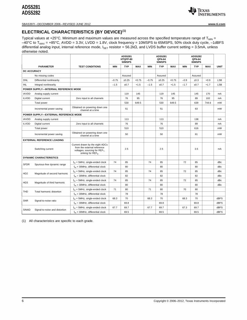
ADS5281ADS5282
SBAS397I ndashDECEMBER 2006ndashREVISED JUNE 2012 wwwticom
ELECTRICAL CHARACTERISTICS (BY DEVICE) (1)
Typical values at +25degC Minimum and maximum values are measured across the specified temperature range of TMIN =ndash40degC to TMAX = +85degC AVDD = 33V LVDD = 18V clock frequency = 10MSPS to 65MSPS 50 clock duty cycle ndash1dBFSdifferential analog input internal reference mode ISET resistor = 562kΩ and LVDS buffer current setting = 35mA unlessotherwise noted
ADS5281 ADS5281 ADS5282HTQFP-80 QFN-64 QFN-6450MSPS 50MSPS 65MSPS
PARAMETER TEST CONDITIONS MIN TYP MAX MIN TYP MAX MIN TYP MAX UNIT
DC ACCURACY
No missing codes Assured Assured Assured
DNL Differential nonlinearity ndash075 plusmn025 +075 ndash075 plusmn025 +075 ndash09 plusmn03 +09 LSB
INL Integral nonlinearity ndash15 plusmn07 +15 ndash15 plusmn07 +15 ndash17 plusmn07 +17 LSB
POWER SUPPLYmdashINTERNAL REFERENCE MODE
IAVDD Analog supply current 119 145 119 145 145 170 mA
ILVDD Digital current Zero input to all channels 76 95 76 95 89 102 mA
Total power 530 6495 530 6495 639 7446 mW
Obtained on powering down oneIncremental power saving 51 51 63 mW
channel at a time
POWER SUPPLYmdashEXTERNAL REFERENCE MODE
IAVDD Analog supply current 113 113 138 mA
ILVDD Digital current Zero input to all channels 76 76 89 mA
Total power 510 510 616 mW
Obtained on powering down oneIncremental power saving 50 50 61 mW
channel at a time
EXTERNAL REFERENCE LOADING
Current drawn by the eight ADCsfrom the external reference
Switching current 25 25 35 mAvoltages sourcing for REFT
sinking for REFB
DYNAMIC CHARACTERISTICS
fIN = 5MHz single-ended clock 74 85 74 85 72 85 dBcSFDR Spurious-free dynamic range
fIN = 30MHz differential clock 80 80 80 dBc
fIN = 5MHz single-ended clock 74 85 74 85 72 85 dBcHD2 Magnitude of second harmonic
fIN = 30MHz differential clock 82 82 82 dBc
fIN = 5MHz single-ended clock 74 85 74 85 72 85 dBcHD3 Magnitude of third harmonic
fIN = 30MHz differential clock 80 80 80 dBc
fIN = 5MHz single-ended clock 71 80 71 80 70 80THD Total harmonic distortion
fIN = 30MHz differential clock 78 78 78
fIN = 5MHz single-ended clock 683 70 683 70 683 70 dBFSSNR Signal-to-noise ratio
fIN = 30MHz differential clock 698 698 698 dBFS
fIN = 5MHz single-ended clock 677 697 677 697 673 697 dBFSSINAD Signal-to-noise and distortion
fIN = 30MHz differential clock 695 695 695 dBFS
(1) All characteristics are specific to each grade
6 Copyright copy 2006ndash2012 Texas Instruments Incorporated
60
59
58
57
56
55
54
53
52
51
50
49
48
47
46
45
44
43
42
41
AVDD
IN8N
IN8P
AVSS
IN7N
IN7P
AVDD
AVSS
IN6N
IN6P
AVSS
IN5N
IN5P
AVDD
LVSS
RESET
LVSS
LVSS
ADCLKN
ADCLKP
AV
SS
OU
T1
P
AV
SS
OU
T1
N
SC
LK
OU
T2
P
SD
ATA
OU
T2
N
CS
LV
DD
AV
DD
LV
SS
AV
SS
OU
T3
P
AV
SS
OU
T3
N
CLK
NO
UT
4P
CLK
PO
UT
4N
AV
DD
OU
T5
P
INT
EX
TO
UT
5N
AV
SS
OU
T6
P
RE
FT
OU
T6
N
RE
FB
LV
DD
VC
MLV
SS
I SE
TO
UT
7P
AV
DD
OU
T7
N
NC
OU
T8
P
TP
OU
T8
N
1
2
3
4
5
6
7
8
9
10
11
12
13
14
15
16
17
18
19
20
AVDD
IN1P
IN1N
AVSS
IN2P
IN2N
AVDD
AVSS
IN3P
IN3N
AVSS
IN4P
IN4N
AVDD
LVSS
PD
LVSS
LVSS
LCLKP
LCLKN
80 79 78 77 76 75 74 73 72 71 70
21 22 23 24 25 26 27 28 29 30 31
69
32 33 34 35 36 37 38 39 40
68 67 66 65 64 63 62 61
ADS528x
ADS5281ADS5282
wwwticom SBAS397I ndashDECEMBER 2006ndashREVISED JUNE 2012
PIN CONFIGURATIONS
TQFP-80TOP VIEW
Table 2 PIN DESCRIPTIONS TQFP-80
PIN NAME DESCRIPTION PIN NUMBER OF PINS
ADCLKN LVDS frame clock (1X)mdashnegative output 42 1
ADCLKP LVDS frame clock (1X)mdashpositive output 41 1
AVDD Analog power supply 33V 1 7 14 47 54 60 63 70 75 9
AVSS Analog ground 4 8 11 50 53 57 68 73 74 79 80 11
Negative differential clockCLKN 72 1Tie CLKN to 0V for a single-ended clock
CLKP Positive differential clock 71 1
CS Serial enable chip selectmdashactive low digital input 76 1
IN1N Negative differential input signal channel 1 3 1
IN1P Positive differential input signal channel 1 2 1
IN2N Negative differential input signal channel 2 6 1
Copyright copy 2006ndash2012 Texas Instruments Incorporated 7
ADS5281ADS5282
SBAS397I ndashDECEMBER 2006ndashREVISED JUNE 2012 wwwticom
Table 2 PIN DESCRIPTIONS TQFP-80 (continued)
PIN NAME DESCRIPTION PIN NUMBER OF PINS
IN2P Positive differential input signal channel 2 5 1
IN3N Negative differential input signal channel 3 10 1
IN3P Positive differential input signal channel 3 9 1
IN4N Negative differential input signal channel 4 13 1
IN4P Positive differential input signal channel 4 12 1
IN5N Negative differential input signal channel 5 49 1
IN5P Positive differential input signal channel 5 48 1
IN6N Negative differential input signal channel 6 52 1
IN6P Positive differential input signal channel 6 51 1
IN7N Negative differential input signal channel 7 56 1
IN7P Positive differential input signal channel 7 55 1
IN8N Negative differential input signal channel 8 59 1
IN8P Positive differential input signal channel 8 58 1
INTEXT Internalexternal reference mode select input 69 1
ISET Bias pinmdash562kΩ to ground 64 1
LCLKN LVDS bit clock (6X)mdashnegative output 20 1
LCLKP LVDS bit clock (6X)mdashpositive output 19 1
LVDD Digital and IO power supply 18V 25 35 2
LVSS Digital ground 15 17 18 26 36 43 44 46 8
NC No connection (or connect to ground) 62 1
OUT1N LVDS channel 1mdashnegative output 22 1
OUT1P LVDS channel 1mdashpositive output 21 1
OUT2N LVDS channel 2mdashnegative output 24 1
OUT2P LVDS channel 2mdashpositive output 23 1
OUT3N LVDS channel 3mdashnegative output 28 1
OUT3P LVDS channel 3mdashpositive output 27 1
OUT4N LVDS channel 4mdashnegative output 30 1
OUT4P LVDS channel 4mdashpositive output 29 1
OUT5N LVDS channel 5mdashnegative output 32 1
OUT5P LVDS channel 5mdashpositive output 31 1
OUT6N LVDS channel 6mdashnegative output 34 1
OUT6P LVDS channel 6mdashpositive output 33 1
OUT7N LVDS channel 7mdashnegative output 38 1
OUT7P LVDS channel 7mdashpositive output 37 1
OUT8N LVDS channel 8mdashnegative output 40 1
OUT8P LVDS channel 8mdashpositive output 39 1
PD Power-down input 16 1
REFB Negative reference inputoutput 66 1
REFT Positive reference inputoutput 67 1
RESET Active low RESET input 45 1
SCLK Serial clock input 78 1
SDATA Serial data input 77 1
TP Test pin do not use 61 1
VCM Common-mode output pin 15V output 65 1
8 Copyright copy 2006ndash2012 Texas Instruments Incorporated
48
47
46
45
44
43
42
41
40
39
38
37
36
35
34
33
IN8N
IN8P
AVSS
IN7N
IN7P
AVSS
IN6N
IN6P
AVSS
IN5N
IN5P
AVSS
LVSS
LVDD
OUT8N
OUT8P
1
2
3
4
5
6
7
8
9
10
11
12
13
14
15
16
IN1P
IN1N
AVSS
IN2P
IN2N
AVSS
IN3P
IN3N
AVSS
IN4P
IN4N
LVSS
PD
LVSS
OUT1P
OUT1N
RE
SE
T
SC
LK
SD
ATA
CS
AV
DD
CLK
N
CLK
P
AV
DD
INT
EX
T
RE
FT
RE
FB
VC
M
TP
I SE
T
AV
DD
AV
DD
OU
T2
P
OU
T2
N
OU
T3
P
OU
T3
N
OU
T4
P
OU
T4
N
AD
CLK
P
AD
CLK
N
LC
LK
P
LC
LK
N
OU
T5
P
OU
T5
N
OU
T6
P
OU
T6
N
OU
T7
P
OU
T7
N
64 63 62 61 60 59 58 57 56 55 54
17 18 19 20 21 22 23 24 25 26 27
53 52 51 50 49
28 29 30 31 32
ADS528X
ADS5281ADS5282
wwwticom SBAS397I ndashDECEMBER 2006ndashREVISED JUNE 2012
QFN-64 PowerPADTOP VIEW
Table 3 PIN DESCRIPTIONS QFN-64
PIN NAME DESCRIPTION PIN NUMBER OF PINS
ADCLKN LVDS frame clock (1X)mdashnegative output 24 1
ADCLKP LVDS frame clock (1X)mdashpositive output 23 1
AVDD Analog power supply 33V 49 50 57 60 4
AVSS Analog ground 3 6 9 37 40 43 46 7
Negative differential clock inputCLKN 59 1Tie CLKN to 0V for a single-ended clock
CLKP Positive differential clock input 58 1
CS Serial enable chip selectmdashactive low digital input 61 1
IN1N Negative differential input signal channel 1 2 1
IN1P Positive differential input signal channel 1 1 1
IN2N Negative differential input signal channel 2 5 1
IN2P Positive differential input signal channel 2 4 1
IN3N Negative differential input signal channel 3 8 1
IN3P Positive differential input signal channel 3 7 1
IN4N Negative differential input signal channel 4 11 1
IN4P Positive differential input signal channel 4 10 1
IN5N Negative differential input signal channel 5 39 1
Copyright copy 2006ndash2012 Texas Instruments Incorporated 9
ADS5281ADS5282
SBAS397I ndashDECEMBER 2006ndashREVISED JUNE 2012 wwwticom
Table 3 PIN DESCRIPTIONS QFN-64 (continued)
PIN NAME DESCRIPTION PIN NUMBER OF PINS
IN5P Positive differential input signal channel 5 38 1
IN6N Negative differential input signal channel 6 42 1
IN6P Positive differential input signal channel 6 41 1
IN7N Negative differential input signal channel 7 45 1
IN7P Positive differential input signal channel 7 44 1
IN8N Negative differential input signal channel 8 48 1
IN8P Positive differential input signal channel 8 47 1
INTEXT Internalexternal reference mode select input 56 1
ISET Bias pinmdash562kΩ to ground 51 1
LCLKN LVDS bit clock (6X)mdashnegative output 26 1
LCLKP LVDS bit clock (6X)mdashpositive output 25 1
LVDD Digital and IO power supply 18V 35 1
LVSS Digital ground 12 14 36 3
OUT1N LVDS channel 1mdashnegative output 16 1
OUT1P LVDS channel 1mdashpositive output 15 1
OUT2N LVDS channel 2mdashnegative output 18 1
OUT2P LVDS channel 2mdashpositive output 17 1
OUT3N LVDS channel 3mdashnegative output 20 1
OUT3P LVDS channel 3mdashpositive output 19 1
OUT4N LVDS channel 4mdashnegative output 22 1
OUT4P LVDS channel 4mdashpositive output 21 1
OUT5N LVDS channel 5mdashnegative output 28 1
OUT5P LVDS channel 5mdashpositive output 27 1
OUT6N LVDS channel 6mdashnegative output 30 1
OUT6P LVDS channel 6mdashpositive output 29 1
OUT7N LVDS channel 7mdashnegative output 32 1
OUT7P LVDS channel 7mdashpositive output 31 1
OUT8N LVDS channel 8mdashnegative output 34 1
OUT8P LVDS channel 8mdashpositive output 33 1
PD Power-down input 13 1
REFB Negative reference inputoutput 54 1
REFT Positive reference inputoutput 55 1
RESET Active low RESET input 64 1
SCLK Serial clock input 63 1
SDATA Serial data input 62 1
TP Test pin do not use 52 1
VCM Common-mode output pin 15V output 53 1
10 Copyright copy 2006ndash2012 Texas Instruments Incorporated
12-BitADC
PLL
Serializer
1x ADCLK
6x ADCLK
IN1P
IN1N
OUT1P
OUT1N
12-BitADC
SerializerIN2P
IN2N
OUT2P
OUT2N
12-BitADC
SerializerIN3P
IN3N
OUT3P
OUT3N
LCLKP
LCLKN
ADCLKP
ADCLKN
12x ADCLK
12-BitADC
SerializerIN4P
IN4N
OUT4P
OUT4N
12-BitADC
SerializerIN5P
IN5N
OUT5P
OUT5N
12-BitADC
SerializerIN6P
IN6N
OUT6P
OUT6N
12-BitADC
SerializerIN7P
IN7N
OUT7P
OUT7N
12-BitADC
Serializer
Digital
Digital
Digital
Digital
Digital
Digital
Digital
Digital
Reference
IN8P
IN8N
RE
FT
INT
EX
T
RE
FB
VC
M
OUT8P
OUT8N
I SE
T
Registers
SD
ATA
CS
RE
SE
T
SC
LK
ADC
Control
PD
Clock
Buffer
(AD
CL
K)
CL
KP
(AV
SS
)
CL
KN
AV
DD
(33
V)
LV
DD
(18
V)
Power-
Down
Te
st
Pa
tte
rns
Drive
Cu
rre
nt
Ou
tpu
t F
orm
at
Dig
ita
l G
ain
(0d
B-1
2d
B)
ADS5281ADS5282
wwwticom SBAS397I ndashDECEMBER 2006ndashREVISED JUNE 2012
FUNCTIONAL BLOCK DIAGRAM
Copyright copy 2006ndash2012 Texas Instruments Incorporated 11
tH1
tSU1
tH2
tSU2
LCLKN
LCLKP
OUTN
OUTP
D0 D1 D2 D3 D4 D5 D6 D7 D8 D9 D10 D11 D0 D1 D2 D3 D4 D5 D6 D7 D8 D9 D10 D11D0 D1 D2 D3 D4 D5 D6 D7 D8 D9 D10 D11
Sample nSample n + 12
tPROP
t (A)D
12 clocks latency
Analog Input
Clock Input
6X ADCLK
LCLKN
LCLKP
1X ADCLK
ADCLKN
ADCLKP
SERIAL DATA
OUTP
OUTN
tSAMPLE
Sample n + 13
ADS5281ADS5282
SBAS397I ndashDECEMBER 2006ndashREVISED JUNE 2012 wwwticom
LVDS TIMING DIAGRAM
DEFINITION OF SETUP AND HOLD TIMES
tSU = min(tSU1 tSU2)
tH = min(tH1 tH2)
TIMING CHARACTERISTICS (1) (2)
ADS528x
PARAMETER TEST CONDITIONS MIN TYP MAX UNIT
tA Aperture delay 15 45 ns
Aperture delay variation Channel-to-channel within the same device (3σ) plusmn20 ps
tJ Aperture jitter 400 fs
Time to valid data after coming out of 50 μsCOMPLETE POWER-DOWN mode
Time to valid data after coming out of PARTIALtWAKE Wake-up time POWER-DOWN mode (with clock continuing to 2 μs
run during power-down)
Time to valid data after stopping and restarting 40 μsthe input clock
ClockData latency 12 cycles
(1) Timing characteristics are common to the ADS528x family(2) Timing parameters are ensured by design and characterization not production tested
12 Copyright copy 2006ndash2012 Texas Instruments Incorporated
ADS5281ADS5282
wwwticom SBAS397I ndashDECEMBER 2006ndashREVISED JUNE 2012
LVDS OUTPUT TIMING CHARACTERISTICS (1) (2)
Typical values are at +25degC minimum and maximum values are measured across the specified temperature range of TMIN = ndash40degC to TMAX =+85degC sampling frequency = as specified CLOAD = 5pF (3) IOUT = 35mA RLOAD = 100Ω (4) and no internal termination unless otherwisenoted
ADS528x
40MSPS 50MSPS 65MSPS
PARAMETER TEST CONDITIONS (5) MIN TYP MAX MIN TYP MAX MIN TYP MAX UNIT
Data valid (7) to zero-crossing oftSU Data setup time(6) 067 047 027 ns
LCLKP
Zero-crossing of LCLKP to datatH Data hold time(6) 085 065 04 ns
becoming invalid(7)
Input clock (ADCLK) rising edgetPROP Clock propagation delay cross-over to output clock (ADCLKP) 10 14 166 10 125 141 97 115 14 ns
rising edge cross-over
Duty cycle of differential clockLVDS bit clock duty cycle 455 50 53 45 50 535 41 50 57
(LCLKP ndash LCLKN)
Bit clock cycle-to-cycle250 250 250 ps pp
jitter
Frame clock cycle-to-cycle150 150 150 ps pp
jitter
tRISE Data rise time data fall Rise time is from ndash100mV to +100mV009 02 04 009 02 04 009 02 04 ns
tFALL time Fall time is from +100mV to ndash100mV
tCLKRISE Output clock rise time Rise time is from ndash100mV to +100mV009 02 04 009 02 04 009 02 04 ns
tCLKFALL output clock fall time Fall time is from +100mV to ndash100mV
(1) All characteristics are at the maximum rated speed for each speed grade(2) Timing parameters are ensured by design and characterization not production tested(3) CLOAD is the effective external single-ended load capacitance between each output pin and ground(4) IOUT refers to the LVDS buffer current setting RLOAD is the differential load resistance between the LVDS output pair(5) Measurements are done with a transmission line of 100Ω characteristic impedance between the device and the load(6) Setup and hold time specifications take into account the effect of jitter on the output data and clock These specifications also assume
that data and clock paths are perfectly matched within the receiver Any mismatch in these paths within the receiver would appear asreduced timing margin
(7) Data valid refers to a logic high of +100mV and a logic low of ndash100mV
LVDS OUTPUT TIMING CHARACTERISTICS (1) (2)
Typical values are at +25degC minimum and maximum values are measured across the specified temperature range of TMIN = ndash40degC to TMAX =+85degC sampling frequency = as specified CLOAD = 5pF (3) IOUT = 35mA RLOAD = 100Ω (4) and no internal termination unless otherwisenoted
ADS528x
30MSPS 20MSPS 10MSPS
PARAMETER TEST CONDITIONS (5) MIN TYP MAX MIN TYP MAX MIN TYP MAX UNIT
Data valid (7) to zero-crossing oftSU Data setup time(6) 08 15 37 ns
LCLKP
Zero-crossing of LCLKP to datatH Data hold time(6) 12 19 39 ns
becoming invalid(7)
Input clock (ADCLK) rising edgetPROP Clock propagation delay cross-over to output clock (ADCLKP) 95 135 173 95 145 173 10 147 171 ns
rising edge cross-over
Duty cycle of differential clockLVDS bit clock duty cycle 465 50 52 48 50 51 49 50 51
(LCLKP ndash LCLKN)
Bit clock cycle-to-cycle250 250 750 ps pp
jitter
Frame clock cycle-to-cycle150 150 500 ps pp
jitter
tRISE Data rise time data fall Rise time is from ndash100mV to +100mV009 02 04 009 02 04 009 02 04 ns
tFALL time Fall time is from +100mV to ndash100mV
tCLKRISE Output clock rise time Rise time is from ndash100mV to +100mV009 02 04 009 02 04 009 02 04 ns
tCLKFALL output clock fall time Fall time is from +100mV to ndash100mV
(1) All characteristics are at the speeds other than the maximum rated speed for each speed grade(2) Timing parameters are ensured by design and characterization not production tested(3) CLOAD is the effective external single-ended load capacitance between each output pin and ground(4) IOUT refers to the LVDS buffer current setting RLOAD is the differential load resistance between the LVDS output pair(5) Measurements are done with a transmission line of 100Ω characteristic impedance between the device and the load(6) Setup and hold time specifications take into account the effect of jitter on the output data and clock These specifications also assume
that data and clock paths are perfectly matched within the receiver Any mismatch in these paths within the receiver would appear asreduced timing margin
(7) Data valid refers to a logic high of +100mV and a logic low of ndash100mV
Copyright copy 2006ndash2012 Texas Instruments Incorporated 13
t1
t2
t3
AVDD (3V to 36V)
LVDD (17V to 19V)
High-Level RESET
(14V to 36V)
High-Level CS
(14V to 36V)
Device Ready for
Serial Register Write(2)
Device Ready for
Data ConversionStart of Clock
AVDD
LVDD
RESET
CS
ADCLK
t4 t7
t5
t8
t6
ADS5281ADS5282
SBAS397I ndashDECEMBER 2006ndashREVISED JUNE 2012 wwwticom
LVDS OUTPUT TIMING CHARACTERISTICSTIMINGS WHEN USING REGISTER 0xE3 (2)
At 40 MSPSPARAMETER (1) TEST CONDITIONS
MIN TYP MAX
Data setup time Data valid (3) to zero-crossing of LCLKp 060
Data hold time Zero-crossing of LCLKP to data becoming invalid(3) 092
Input clock (ADCLK) rising edge cross-over to output clock (ADCLK) rising edgeClock propagation delay 8 12 146
crossover
(1) Only the setup time hold time and clock propagation delay parameters are affected Rest of the parameters are same as given inprevious two tables
(2) Only timing specifications for 40MSPS are affected when using register 0xE3 (as specified in the recommended operating table section)The timing specifications for other clock frequencies are same as given in previous two tables
(3) Data valid refers to logic high of +100mV and logic low of ndash100mV
RECOMMENDED POWER-UP SEQUENCING AND RESET TIMING
10μs lt t1 lt 50ms 10μs lt t2 lt 50ms ndash10ms lt t3 lt 10ms t4 gt 10ms t5 gt 100ns t6 gt 100ns t7 gt 10ms and t8 gt 100μs
(1) The AVDD and LVDD power on sequence does not matter as long as ndash10ms lt t3 lt 10ms Similar considerations apply while shuttingdown the device
(2) Write initialization registers listed in the Initialization Registers table
14 Copyright copy 2006ndash2012 Texas Instruments Incorporated
PD
Device Fully
Powers DownDevice Fully
Powers Up
tWAKE1 sm
ADS5281ADS5282
wwwticom SBAS397I ndashDECEMBER 2006ndashREVISED JUNE 2012
POWER-DOWN TIMING
Power-up time shown is based on 1μF bypass capacitors on the reference pins tWAKE is the time it takes for the device to wake upcompletely from power-down mode The ADS528x has two power-down modes complete power-down mode and partial power-down modeThe device can be configured in partial power-down mode through a register setting
tWAKE lt 50μs for complete power-down mode
tWAKE lt 2μs for partial power-down mode (provided the clock is not shut off during power-down)
Copyright copy 2006ndash2012 Texas Instruments Incorporated 15
D15 D14 D13 D12 D11 D10 D9 D8 D7 D6 D5 D4 D3 D2 D1 D0A7 A6 A5 A4 A3 A2 A1 A0
CS
SCLK
SDATA
Data latched on rising edge of SCLK
Start Sequence End Sequence
t6
t4
t2
t7
t3
t5
t1
ADS5281ADS5282
SBAS397I ndashDECEMBER 2006ndashREVISED JUNE 2012 wwwticom
SERIAL INTERFACE
The ADS528x has a set of internal registers that can be accessed through the serial interface formed by pins CS(chip select active low) SCLK (serial interface clock) and SDATA (serial interface data) When CS is low thefollowing actions occurbull Serial shift of bits into the device is enabledbull SDATA (serial data) is latched at every rising edge of SCLKbull SDATA is loaded into the register at every 24th SCLK rising edge
If the word length exceeds a multiple of 24 bits the excess bits are ignored Data can be loaded in multiples of24-bit words within a single active CS pulse The first eight bits form the register address and the remaining 16bits form the register data The interface can work with SCLK frequencies from 20MHz down to very low speeds(a few hertz) and also with a non-50 SCLK duty cycle
Register Initialization
After power-up the internal registers must be initialized to the respective default values Initialization can bedone in one of two ways1 Through a hardware reset by applying a low-going pulse on the RESET pin or2 Through a software reset using the serial interface set the RST bit high Setting this bit initializes the
internal registers to the respective default values and then self-resets the RST bit low In this case theRESET pin stays high (inactive)
After all registers have been initialized to their default values through a RESET operation the registers detailedin the Initialization Registers table must be written into This process must be done after every hardware orsoftware RESET operation in order to reconfigure the device for the best mode of operation
SERIAL INTERFACE TIMING
ADS528x
PARAMETER DESCRIPTION MIN TYP MAX UNIT
t1 SCLK period 50 ns
t2 SCLK high time 20 ns
t3 SCLK low time 20 ns
t4 Data setup time 5 ns
t5 Data hold time 5 ns
t6 CS fall to SCLK rise 8 ns
t7 Time between last SCLK rising edge to CS rising edge 8 ns
16 Copyright copy 2006ndash2012 Texas Instruments Incorporated
ADS5281ADS5282
wwwticom SBAS397I ndashDECEMBER 2006ndashREVISED JUNE 2012
SERIAL REGISTER MAP
Table 4 SUMMARY OF FUNCTIONS SUPPORTED BY SERIAL INTERFACE (1) (2) (3) (4)
ADDRESSIN HEX D15 D14 D13 D12 D11 D10 D9 D8 D7 D6 D5 D4 D3 D2 D1 D0 NAME DESCRIPTION DEFAULT
00 X RST Self-clearing software RESET Inactive
Channel-specific ADC power-X X X X X X X X PDN_CHlt81gt Inactive
down mode
Partial power-down mode (fastX PDN_PARTIAL Inactive
recovery from power-down)0F
Register mode for completeX PDN_COMPLETE Inactive
power-down (slower recovery)
Configures the PD pin for partial CompleteX PDN_PIN_CFG
power-down mode power-down
LVDS current driveX X X ILVDS_LCLKlt20gt programmability for LCLKN and 35mA drive
LCLKP pins
LVDS current driveILVDS_FRAME
11 X X X programmability for ADCLKN and 35mA drivelt20gt
ADCLKP pins
LVDS current driveX X X ILVDS_DATlt20gt programmability for OUTN and 35mA drive
OUTP pins
Enables internal termination for TerminationX EN_LVDS_TERM
LVDS buffers disabled
Programmable termination for Termination1 X X X TERM_LCLKlt20gt
LCLKN and LCLKP buffers disabled12
TERM_FRAME Programmable termination for Termination1 X X X
lt20gt ADCLKN and ADCLKP buffers disabled
Programmable termination for Termination1 X X X TERM_DATlt20gt
OUTN and OUTP buffers disabled
Channel-specific low-frequency14 X X X X X X X X LFNS_CHlt81gt Inactive
noise suppression mode enable
INP isSwaps the polarity of the analog
24 X X X X X X X X INVERT_CHlt81gt positiveinput pins electrically
input
Enables a repeating full-scaleX 0 0 EN_RAMP Inactive
ramp pattern on the outputs
Enables the mode wherein theDUALCUSTOM_
0 X 0 output toggles between two InactivePAT
defined codes
Enables the mode wherein theSINGLE_CUSTOM
0 0 X output is a constant specified Inactive25 _PAT
code
2MSBs for a single customBITS_CUSTOM1 pattern (and for the first code of
X X Inactivelt1110gt the dual custom pattern) lt11gt is
the MSB
BITS_CUSTOM2 2MSBs for the second code ofX X Inactive
lt1110gt the dual custom pattern
10 lower bits for the singleBITS_CUSTOM1 custom pattern (and for the first
26 X X X X X X X X X X Inactivelt90gt code of the dual custom pattern)
lt0gt is the LSB
BITS_CUSTOM2 10 lower bits for the second27 X X X X X X X X X X Inactive
lt90gt code of the dual custom pattern
X X X X GAIN_CH1lt30gt Programmable gain channel 1 0dB gain
X X X X GAIN_CH2lt30gt Programmable gain channel 2 0dB gain2A
X X X X GAIN_CH3lt30gt Programmable gain channel 3 0dB gain
X X X X GAIN_CH4lt30gt Programmable gain channel 4 0dB gain
X X X X GAIN_CH5lt30gt Programmable gain channel 5 0dB gain
X X X X GAIN_CH6lt30gt Programmable gain channel 6 0dB gain2B
X X X X GAIN_CH7lt30gt Programmable gain channel 7 0dB gain
X X X X GAIN_CH8lt30gt Programmable gain channel 8 0dB gain
(1) The unused bits in each register (identified as blank table cells) must be programmed as 0(2) X = Register bit referenced by the corresponding name and description (default is 0)(3) Bits marked as 0 should be forced to 0 and bits marked as 1 should be forced to 1 when the particular register is programmed(4) Multiple functions in a register should be programmed in a single write operation
Copyright copy 2006ndash2012 Texas Instruments Incorporated 17
ADS5281ADS5282
SBAS397I ndashDECEMBER 2006ndashREVISED JUNE 2012 wwwticom
Table 4 SUMMARY OF FUNCTIONS SUPPORTED BY SERIAL INTERFACE(1) (2) (3) (4) (continued)ADDRESS
IN HEX D15 D14 D13 D12 D11 D10 D9 D8 D7 D6 D5 D4 D3 D2 D1 D0 NAME DESCRIPTION DEFAULT
Single-1 X DIFF_CLK Differential clock mode
ended clock
Enables the duty-cycle correction1 X EN_DCC Disabled
circuit
External42Drives the external reference reference
1 X EXT_REF_VCMmode through the VCM pin drives REFT
and REFB
Controls the phase of LCLK1 X X PHASE_DDRlt10gt 90 degrees
output relative to data
0 X PAT_DESKEW Enables deskew pattern mode Inactive45
X 0 PAT_SYNC Enables sync pattern mode Inactive
Binary twos complement format Straight1 1 X BTC_MODE
for ADC output offset binary
Serialized ADC output comes LSB-first1 1 X MSB_FIRST
out MSB-first output
Enables SDR output modeDDR output46 1 1 X EN_SDR (LCLK becomes a 12x input
modeclock)
Controls whether the LCLK rising Rising edgeor falling edge comes in the of LCLK in
1 X 1 1 FALL_SDRmiddle of the data window when middle ofoperating in SDR output mode data window
SUMMARY OF FEATURES
POWER IMPACT (relative to default)FEATURES DEFAULT SELECTION AT fS = 65MSPS
ANALOG FEATURES
Internal or external reference Internal reference mode uses approximately 23mW moreNA Pin(driven on the REFT and REFB pins) power on AVDD
External reference driven on the Off Register 42 Approximately 9mW less power on AVDDVCM pin
Duty cycle correction circuit Off Register 42 Approximately 7mW more power on AVDD
With zero input to the ADC low-frequency noise suppressionLow-frequency noise suppression Off Register 14 causes digital switching at fS2 thereby increasing LVDD
power by approximately 7mWchannel
Differential clock mode uses approximately 7mW more powerSingle-ended or differential clock Single-ended Register 42 on AVDD
Refer to the Power-Down Modes section in the ElectricalPower-down mode Off Pin and register 0F Characteristics table
DIGITAL FEATURES
Programmable digital gain (0dB to Registers 2A and0dB No difference12dB) 2B
Straight offset or BTC output Straight offset Register 46 No difference
Swap polarity of analog input pins Off Register 24 No difference
LVDS OUTPUT PHYSICAL LAYER
LVDS internal termination Off Register 12 Approximately 7mW more power on AVDD
LVDS current programmability 35mA Register 11 As per LVDS clock and data buffer current setting
LVDS OUTPUT TIMING
LSB- or MSB-first output LSB-first Register 46 No difference
SDR mode uses approximately 2mW more power on LVDDDDR or SDR output DDR Register 46 (at fS = 30MSPS)
Refer toLCLK phase relative to data output Register 42 No differenceFigure 1
18 Copyright copy 2006ndash2012 Texas Instruments Incorporated
ADS5281ADS5282
wwwticom SBAS397I ndashDECEMBER 2006ndashREVISED JUNE 2012
DESCRIPTION OF SERIAL REGISTERS
SOFTWARE RESET
ADDRESSIN HEX D15 D14 D13 D12 D11 D10 D9 D8 D7 D6 D5 D4 D3 D2 D1 D0 NAME
00 X RST
Software reset is applied when the RST bit is set to 1 setting this bit resets all internal registers and self-clearsto 0
POWER-DOWN MODES
ADDRESSIN HEX D15 D14 D13 D12 D11 D10 D9 D8 D7 D6 D5 D4 D3 D2 D1 D0 NAME
X X X X X X X X PDN_CHlt81gt
X PDN_PARTIAL0F
0 X PDN_COMPLETE
X 0 PDN_PIN_CFG
Each of the eight channels can be individually powered down PDN_CHltNgt controls the power-down mode forthe ADC channel ltNgt
In addition to channel-specific power-down the ADS528x also has two global power-down modesmdashpartialpower-down mode and complete power-down mode Partial power-down mode partially powers down the chiprecovery from this mode is much quicker provided that the clock has been running for at least 50μs beforeexiting this mode Complete power-down mode on the other hand completely powers down the chip andinvolves a much longer recovery time
In addition to programming the device for either of these two power-down modes (through either thePDN_PARTIAL or PDN_COMPLETE bits respectively) the PD pin itself can be configured as either a partialpower-down pin or a complete power-down pin control For example if PDN_PIN_CFG = 0 (default) when thePD pin is high the device enters complete power-down mode However if PDN_PIN_CFG = 1 when the PD pinis high the device enters partial power-down mode
LVDS DRIVE PROGRAMMABILITY
ADDRESSIN HEX D15 D14 D13 D12 D11 D10 D9 D8 D7 D6 D5 D4 D3 D2 D1 D0 NAME
X X X ILVDS_LCLKlt20gt
11 X X X ILVDS_FRAMElt20gt
X X X ILVDS_DATlt20gt
The LVDS drive strength of the bit clock (LCLKP or LCLKN) and the frame clock (ADCLKP or ADCLKN) can beindividually programmed The LVDS drive strengths of all the data outputs OUTP and OUTN can also beprogrammed to the same value
Copyright copy 2006ndash2012 Texas Instruments Incorporated 19
ADS5281ADS5282
SBAS397I ndashDECEMBER 2006ndashREVISED JUNE 2012 wwwticom
All three drive strengths (bit clock frame clock and data) are programmed using sets of three bits Table 5shows an example of how the drive strength of the bit clock is programmed (the method is similar for the frameclock and data drive strengths)
Table 5 Bit Clock Drive Strength (1)
ILVDS_LCLKlt2gt ILVDS_LCLKlt1gt ILVDS_LCLKlt0gt LVDS DRIVE STRENGTH FOR LCLKP AND LCLKN
0 0 0 35mA (default)
0 0 1 25mA
0 1 0 15mA
0 1 1 05mA
1 0 0 75mA
1 0 1 65mA
1 1 0 55mA
1 1 1 45mA
(1) Current settings lower than 15mA are not recommended
LVDS INTERNAL TERMINATION PROGRAMMABILITY
ADDRESSIN HEX D15 D14 D13 D12 D11 D10 D9 D8 D7 D6 D5 D4 D3 D2 D1 D0 NAME
X EN_LVDS_TERM
1 X X X TERM_LCLKlt20gt12
1 X X X TERM_FRAMElt20gt
1 X X X TERM_DATlt20gt
The LVDS buffers have high-impedance current sources driving the outputs When driving traces whosecharacteristic impedance is not perfectly matched with the termination impedance on the receiver side there maybe reflections back to the LVDS output pins of the ADS528x that cause degraded signal integrity By enabling aninternal termination (between the positive and negative outputs) for the LVDS buffers the signal integrity can besignificantly improved in such scenarios To set the internal termination mode the EN_LVDS_TERM bit shouldbe set to 1 Once this bit is set the internal termination values for the bit clock frame clock and data bufferscan be independently programmed using sets of three bits Table 6 shows an example of how the internaltermination of the LVDS buffer driving the bit clock is programmed (the method is similar for the frame clock anddata buffers) These termination values are only typical values and can vary by up to plusmn20 across temperatureand from device to device
Table 6 Bit Clock Internal Termination
INTERNAL TERMINATION BETWEENTERM_LCLKlt2gt TERM_LCLKlt1gt TERM_LCLKlt0gt LCLKP AND LCLKN IN Ω
0 0 0 None
0 0 1 260
0 1 0 150
0 1 1 94
1 0 0 125
1 0 1 80
1 1 0 66
1 1 1 55
20 Copyright copy 2006ndash2012 Texas Instruments Incorporated
ADS5281ADS5282
wwwticom SBAS397I ndashDECEMBER 2006ndashREVISED JUNE 2012
LOW-FREQUENCY NOISE SUPPRESSION MODE
ADDRESSIN HEX D15 D14 D13 D12 D11 D10 D9 D8 D7 D6 D5 D4 D3 D2 D1 D0 NAME
14 X X X X X X X X LFNS_CHlt81gt
The low-frequency noise suppression mode is specifically useful in applications where good noise performance isdesired in the frequency band of 0MHz to 1MHz (around dc) Setting this mode shifts the low-frequency noise ofthe ADS528x to approximately fS2 thereby moving the noise floor around dc to a much lower valueLFNS_CHlt81gt enables this mode individually for each channel
ANALOG INPUT INVERT
ADDRESSIN HEX D15 D14 D13 D12 D11 D10 D9 D8 D7 D6 D5 D4 D3 D2 D1 D0 NAME
24 X X X X X X X X INVERT_CHlt81gt
Normally the INP pin represents the positive analog input pin and INN represents the complementary negativeinput Setting the bits marked INVERT_CHlt81gt (individual control for each channel) causes the inputs to beswapped INN now represents the positive input and INP the negative input
LVDS TEST PATTERNS
ADDRESSIN HEX D15 D14 D13 D12 D11 D10 D9 D8 D7 D6 D5 D4 D3 D2 D1 D0 NAME
X 0 0 EN_RAMP
0 X 0 DUALCUSTOM_PAT
25 0 0 X SINGLE_CUSTOM_PAT
X X BITS_CUSTOM1lt1110gt
X X BITS_CUSTOM2lt1110gt
26 X X X X X X X X X X BITS_CUSTOM1lt90gt
27 X X X X X X X X X X BITS_CUSTOM2lt90gt
0 X PAT_DESKEW45
X 0 PAT_SYNC
The ADS528x can output a variety of test patterns on the LVDS outputs These test patterns replace the normalADC data output Setting EN_RAMP to 1 causes all the channels to output a repeating full-scale ramp patternThe ramp increments from zero code to full-scale code in steps of 1LSB every clock cycle After hitting the full-scale code it returns back to zero code and ramps again
The device can also be programmed to output a constant code by setting SINGLE_CUSTOM_PAT to 1 andprogramming the desired code in BITS_CUSTOM1lt110gt In this mode BITS_CUSTOM1lt110gt take the placeof the 12-bit ADC data at the output and are controlled by LSB-first and MSB-first modes in the same way asnormal ADC data are
The device may also be made to toggle between two consecutive codes by programming DUAL_CUSTOM_PATto 1 The two codes are represented by the contents of BITS_CUSTOM1lt110gt and BITS_CUSTOM2lt110gt
In addition to custom patterns the device may also be made to output two preset patterns1 Deskew patten Set using PAT_DESKEW this mode replaces the 12-bit ADC output Dlt110gt with the
010101010101 word2 Sync pattern Set using PAT_SYNC the normal ADC word is replaced by a fixed 111111000000 word
Note that only one of the above patterns should be active at any given instant
Copyright copy 2006ndash2012 Texas Instruments Incorporated 21
ADS5281ADS5282
SBAS397I ndashDECEMBER 2006ndashREVISED JUNE 2012 wwwticom
PROGRAMMABLE GAIN
ADDRESSIN HEX D15 D14 D13 D12 D11 D10 D9 D8 D7 D6 D5 D4 D3 D2 D1 D0 NAME
X X X X GAIN_CH1lt30gt
X X X X GAIN_CH2lt30gt2A
X X X X GAIN_CH3lt30gt
X X X X GAIN_CH4lt30gt
X X X X GAIN_CH5lt30gt
X X X X GAIN_CH6lt30gt2B
X X X X GAIN_CH7lt30gt
X X X X GAIN_CH8lt30gt
In applications where the full-scale swing of the analog input signal is much less than the 2VPP range supportedby the ADS528x a programmable gain can be set to achieve the full-scale output code even with a lower analoginput swing The programmable gain not only fills the output code range of the ADC but also enhances the SNRof the device by utilizing quantization information from some extra internal bits The programmable gain for eachchannel can be individually set using a set of four bits indicated as GAIN_CHNlt30gt for Channel N The gainsetting is coded in binary from 0dB to 12dB as shown in Table 7
Table 7 Gain Setting for Channel 1
GAIN_CH1lt3gt GAIN_CH1lt2gt GAIN_CH1lt1gt GAIN_CH1lt0gt CHANNEL 1 GAIN SETTING
0 0 0 0 0dB
0 0 0 1 1dB
0 0 1 0 2dB
0 0 1 1 3dB
0 1 0 0 4dB
0 1 0 1 5dB
0 1 1 0 6dB
0 1 1 1 7dB
1 0 0 0 8dB
1 0 0 1 9dB
1 0 1 0 10dB
1 0 1 1 11dB
1 1 0 0 12dB
1 1 0 1 Do not use
1 1 1 0 Do not use
1 1 1 1 Do not use
22 Copyright copy 2006ndash2012 Texas Instruments Incorporated
VREF = 15V -B
VCM
15V
VREF = 15V +T
VCM
15V
ADS5281ADS5282
wwwticom SBAS397I ndashDECEMBER 2006ndashREVISED JUNE 2012
CLOCK REFERENCE AND DATA OUTPUT MODES
ADDRESSIN HEX D15 D14 D13 D12 D11 D10 D9 D8 D7 D6 D5 D4 D3 D2 D1 D0 NAME
1 X DIFF_CLK
1 X EN_DCC42
1 X EXT_REF_VCM
1 X X PHASE_DDRlt10gt
1 1 X BTC_MODE
1 1 X MSB_FIRST46
1 1 X EN_SDR
1 X 1 1 FALL_SDR
INPUT CLOCK
The ADS528x is configured by default to operate with a single-ended input clockmdashCLKP is driven by a CMOSclock and CLKN is tied to 0 However by programming DIFF_CLK to 1 the device can be made to work with adifferential input clock on CLKP and CLKN Operating with a low-jitter differential clock usually gives better SNRperformance especially at input frequencies greater than 30MHz
In cases where the duty cycle of the input clock falls outside the 45 to 55 range it is recommended to enablean internal duty cycle correction circuit This enabling is done by setting the EN_DCC bit to 1
EXTERNAL REFERENCE
The ADS528x can be made to operate in external reference mode by pulling the INTEXT pin to 0 In this modethe REFT and REFB pins should be driven with voltage levels of 25V and 05V respectively and must haveenough drive strength to drive the switched capacitance loading of the reference voltages by each ADC Theadvantage of using the external reference mode is that multiple ADS528x units can be made to operate with thesame external reference thereby improving parameters such as gain matching across devices However inapplications that do not have an available high drive differential external reference the ADS528x can still bedriven with a single external reference voltage on the VCM pin When EXT_REF_VCM is set as 1 (and theINTEXT pin is set to 0) the VCM pin is configured as an input pin and the voltages on REFT and REFB aregenerated as shown in Equation 1 and Equation 2
(1)
(2)
Copyright copy 2006ndash2012 Texas Instruments Incorporated 23
PHASE_DDRlt10gt = 00
PHASE_DDRlt10gt = 01
PHASE_DDRlt10gt = 10
PHASE_DDRlt10gt = 11
ADCLKP
LCLKP
OUTP
ADCLKP
LCLKP
OUTP
ADCLKP
LCLKP
OUTP
ADCLKP
LCLKP
OUTP
ADCLKP
LCLKP
OUTP
ADS5281ADS5282
SBAS397I ndashDECEMBER 2006ndashREVISED JUNE 2012 wwwticom
BIT CLOCK PROGRAMMABILITY
The output interface of the ADS528x is normally a DDR interface with the LCLK rising edge and falling edgetransitions in the middle of alternate data windows This default phase is shown in Figure 1
Figure 1 Default Phase of LCLK
The phase of LCLK can be programmed relative to the output frame clock and data using bitsPHASE_DDRlt10gt The LCLK phase modes are shown in Figure 2
Figure 2 Phase Programmability Modes for LCLK
24 Copyright copy 2006ndash2012 Texas Instruments Incorporated
EN_SDR = 1 FALL_SDR = 0
EN_SDR = 1 FALL_SDR = 1
ADCLKP
LCLKP
OUTP
ADCLKP
LCLKP
OUTP
ADS5281ADS5282
wwwticom SBAS397I ndashDECEMBER 2006ndashREVISED JUNE 2012
In addition to programming the phase of LCLK in the DDR mode the device can also be made to operate in SDRmode by setting the EN_SDR bit to 1 In this mode the bit clock (LCLK) is output at 12x times the input clock ortwice the rate as in DDR mode Depending on the state of FALL_SDR LCLK may be output in either of the twomanners shown in Figure 3 As can be seen in Figure 3 only the LCLK rising (or falling) edge is used to capturethe output data in SDR mode
Figure 3 SDR Interface Modes
The SDR mode does not work well beyond 40MSPS because the LCLK frequency becomes very high
DATA OUTPUT FORMAT MODES
The ADC output by default is in straight offset binary mode Programming the BTC_MODE bit to 1 inverts theMSB and the output becomes binary twos complement mode
Also by default the first bit of the frame (following the rising edge of ADCLKP) is the LSB of the ADC outputProgramming the MSB_FIRST mode inverts the bit order in the word and the MSB is output as the first bitfollowing the ADCLKP rising edge
Copyright copy 2006ndash2012 Texas Instruments Incorporated 25
0
-
-
-
-
-
-
-
-
-
20
40
60
80
100
120
140
160
180
Input Frequency (MHz)
0 25
Am
plit
ude (
dB
)
2015105
SFDR = 884dBc
SNR = 709dBFS
SINAD = 708dBFS
THD = 875dBc
0
-
-
-
-
-
-
-
-
-
20
40
60
80
100
120
140
160
180
Input Frequency (MHz)
0 25
Am
plit
ude (
dB
)
2015105
SFDR = 856dBc
SNR = 705dBFS
SINAD = 704dBFS
THD = 839dBc
0
-
-
-
-
-
-
-
-
-
20
40
60
80
100
120
140
160
180
Input Frequency (MHz)
0 2 20
Am
plit
ude (
dB
)
1816141210864
SFDR = 853dBc
SNR = 708dBFS
SINAD = 707dBFS
THD = 893dBc
0
-
-
-
-
-
-
-
-
-
20
40
60
80
100
120
140
160
180
Input Frequency (MHz)
0 2 20
Am
plit
ude (
dB
)
1816141210864
SFDR = 828dBc
SNR = 702dBFS
SINAD = 70dBFS
THD = 823dBc
ADS5281ADS5282
SBAS397I ndashDECEMBER 2006ndashREVISED JUNE 2012 wwwticom
TYPICAL CHARACTERISTICSAt TA = +25degC AVDD = +33V LVDD = 18V clock frequency = 65MSPS differential clock mode 1VPP clock amplitude 50
clock duty cycle input frequency = 10MHz ndash1dBFS differential analog input 0dB digital gain setting 15V analog inputcommon-mode low-frequency noise suppression = off internal reference mode ISET resistor = 562kΩ and LVDS buffer
current setting = 35mA unless otherwise noted
SPECTRAL PERFORMANCE SPECTRAL PERFORMANCE(fS = 40MHz fIN = 10MHz) (fS = 40MHz fIN = 25MHz)
Figure 4 Figure 5
SPECTRAL PERFORMANCE SPECTRAL PERFORMANCE(fS = 50MHz fIN = 10MHz) (fS = 50MHz fIN = 25MHz)
Figure 6 Figure 7
26 Copyright copy 2006ndash2012 Texas Instruments Incorporated
0
-20
-40
-60
-80
-100
-120
-140
-180
Input Frequency (MHz)
0 33
Am
plit
ude (
dB
)
2015105
-160
SFDR = 862dBc
SNR = 705dBFS
SNR (0MHz to 1MHz) = 861dBFS
SINAD = 704dBFS
THD = 854dBc
25 30
92
87
82
77
72
67
Input Frequency (MHz)
5 30
Dynam
ic P
erf
orm
ance (
SN
R S
FD
R)
201510 25
SNR (dBFS)
SFDR (dBc)
f = 40MHzS
0
-
-
-
-
-
-
-
-
-
20
40
60
80
100
120
140
160
180
Input Frequency (MHz)
0 33
Am
plit
ude (
dB
)
2015105 25 30
SFDR = 909dBc
SNR = 708dBFS
SINAD = 707dBFS
THD = 904dBc
0
-20
-40
-60
-80
-100
-120
-140
-180
Input Frequency (MHz)
0 33
Am
plit
ude (
dB
)
2015105
-160
SFDR = 874dBc
SNR = 704dBFS
SNR (0MHz to 1MHz) = 819dBFS
SINAD = 703dBFS
THD = 864dBc
25 30
ADS5281ADS5282
wwwticom SBAS397I ndashDECEMBER 2006ndashREVISED JUNE 2012
TYPICAL CHARACTERISTICS (continued)At TA = +25degC AVDD = +33V LVDD = 18V clock frequency = 65MSPS differential clock mode 1VPP clock amplitude 50clock duty cycle input frequency = 10MHz ndash1dBFS differential analog input 0dB digital gain setting 15V analog inputcommon-mode low-frequency noise suppression = off internal reference mode ISET resistor = 562kΩ and LVDS buffercurrent setting = 35mA unless otherwise noted
SPECTRAL PERFORMANCE SPECTRAL PERFORMANCE(fS = 65MHz fIN = 10MHz) (fS = 65MHz fIN = 25MHz)
Figure 8 Figure 9
SPECTRAL PERFORMANCE LOW-FREQUENCY NOISESUPPRESSION MODE ENABLED
(fS = 65MHz fIN = 25MHz) DYNAMIC PERFORMANCE vs INPUT FREQUENCY
Figure 10 Figure 11
Copyright copy 2006ndash2012 Texas Instruments Incorporated 27
95
85
75
65
55
45
35
25
Input Amplitude (dBFS)
Dyn
am
ic P
erf
orm
an
ce
(S
NR
S
FD
R)
SNR (dBFS)
SFDR (dBc)
f = 65MHz
f = 10MHzS
IN
-60 0-50 -40 -30 -20 -10
94
89
84
79
74
69
Clock Amplitude (V Differential)PP
06 23
Dynam
ic P
erf
orm
ance (
SN
R S
FD
R)
1611
SNR (dBFS)
SFDR (dBc)
f = 65MHz
f = 10MHzS
IN
21
95
90
85
80
75
70
65
60
Digital Gain (dB)
0 12
Dyn
am
ic P
erf
orm
an
ce
(S
NR
S
FD
R)
642 8
SNR (dBFS)
SFDR (dBc)
f = 65MHz
f = 10MHzS
IN
10
95
90
85
80
75
70
65
60
AVDD (V)
30 36
Dynam
ic P
erf
orm
ance (
SN
R S
FD
R)
333231 34
SNR (dBFS)
SFDR (dBc)
f = 65MHz
f = 10MHzS
IN
35
92
87
82
77
72
67
Input Frequency (MHz)
5 30
Dynam
ic P
erf
orm
ance (
SN
R S
FD
R)
201510 25
SNR (dBFS)
SFDR (dBc)
f = 50MHzS
97
92
87
82
77
72
67
Input Frequency (MHz)
5 30
Dynam
ic P
erf
orm
ance (
SN
R S
FD
R)
201510 25
SNR (dBFS)
SFDR (dBc)
f = 65MHzS
ADS5281ADS5282
SBAS397I ndashDECEMBER 2006ndashREVISED JUNE 2012 wwwticom
TYPICAL CHARACTERISTICS (continued)At TA = +25degC AVDD = +33V LVDD = 18V clock frequency = 65MSPS differential clock mode 1VPP clock amplitude 50clock duty cycle input frequency = 10MHz ndash1dBFS differential analog input 0dB digital gain setting 15V analog inputcommon-mode low-frequency noise suppression = off internal reference mode ISET resistor = 562kΩ and LVDS buffercurrent setting = 35mA unless otherwise noted
DYNAMIC PERFORMANCE vs INPUT FREQUENCY DYNAMIC PERFORMANCE vs INPUT FREQUENCY
Figure 12 Figure 13
DYNAMIC PERFORMANCE vs DIGITAL GAIN DYNAMIC PERFORMANCE vs AVDD
Figure 14 Figure 15
DYNAMIC PERFORMANCE vs INPUT AMPLITUDE DYNAMIC PERFORMANCE vs CLOCK AMPLITUDE
Figure 16 Figure 17
28 Copyright copy 2006ndash2012 Texas Instruments Incorporated
94
89
84
79
74
69
External Reference Common-Mode Voltage (REF + REF )2 (V)T B
135 165
Dynam
ic P
erf
orm
ance (
SN
R S
FD
R)
150145140
SNR (dBFS)
SFDR (dBc)
f = 65MHz
f = 10MHzS
IN
155 160
External reference differential voltage maintained at 2V
94
89
84
79
74
69
Voltage on V (V)CM
135 165
Dynam
ic P
erf
orm
ance (
SN
R S
FD
R)
150145140
SNR (dBFS)
SFDR (dBc)
f = 65MHz
f = 10MHzS
IN
155 160
94
89
84
79
74
69
Analog Input Common-Mode Voltage (V)
130 170
Dynam
ic P
erf
orm
ance (
SN
R S
FD
R)
140135
SNR (dBFS)
SFDR (dBc)
f = 65MHz
f = 10MHzS
IN
145 165160155150
94
89
84
79
74
69
External Reference Differential Voltage REF REF (V)-T B
16 24
Dynam
ic P
erf
orm
ance (
SN
R S
FD
R)
191817
SNR (dBFS)
SFDR (dBc)
f = 65MHz
f = 10MHzS
IN
20 232221
External reference common-mode voltage
maintained at 15V
ADS5281ADS5282
wwwticom SBAS397I ndashDECEMBER 2006ndashREVISED JUNE 2012
TYPICAL CHARACTERISTICS (continued)At TA = +25degC AVDD = +33V LVDD = 18V clock frequency = 65MSPS differential clock mode 1VPP clock amplitude 50clock duty cycle input frequency = 10MHz ndash1dBFS differential analog input 0dB digital gain setting 15V analog inputcommon-mode low-frequency noise suppression = off internal reference mode ISET resistor = 562kΩ and LVDS buffercurrent setting = 35mA unless otherwise noted
DYNAMIC PERFORMANCE vs ANALOG INPUT COMMON- DYNAMIC PERFORMANCE vs EXTERNAL REFERENCEMODE VOLTAGE DIFFERENTIAL VOLTAGE
Figure 18 Figure 19
DYNAMIC PERFORMANCE vs EXTERNAL REFERENCE DYNAMIC PERFORMANCE vs EXTERNAL REFERENCECOMMON-MODE VOLTAGE FORCED THROUGH VCM
Figure 20 Figure 21
Copyright copy 2006ndash2012 Texas Instruments Incorporated 29
05
04
03
02
01
0
-01
-02
-05
Code (LSB)
0 4096
INL
(L
SB
)
30722048 25601536 35841024512
-04
-03
f = 50MSPS
f = 5MHzS
IN
035
025
015
005
-005
-015
-035
Code (LSB)
0 4096
DN
L (
LS
B)
30722048 25601536 35841024512
-025
f = 50MSPS
f = 5MHzS
IN
60
50
40
30
20
10
0
Code Bin (LSB)
2049
Occurr
ence (
)
20532051 2054
f = 65MSPSS
2050 2052
0 0037 028
5192
4743
10
-10
-30
-50
-70
-90
-110
-130
-150
Input Frequency (MHz)
0 2 20
Am
plit
ude (
dB
)
1816141210864
f = 65MHz
f = 10MHz ( 7dBFS)
f = 161MHz ( 7dBFS)
IMD = 97dBFS
-
-
-
S
1
2
95
90
85
80
75
70
65
60
Clock Duty Cycle ()
35 65
Dynam
ic P
erf
orm
ance (
SN
R S
FD
R)
504540 55
SNR (dBFS)
SFDR (dBc)
f = 65MHz
f = 10MHzS
IN
60
95
85
80
75
70
60
Clock Duty Cycle ()
20 80
Dynam
ic P
erf
orm
ance (
SN
R S
FD
R)
504030 60
SNR (dBFS)
SFDR (dBc)
f = 65MHz
f = 10MHzS
IN
90
70
65
ADS5281ADS5282
SBAS397I ndashDECEMBER 2006ndashREVISED JUNE 2012 wwwticom
TYPICAL CHARACTERISTICS (continued)At TA = +25degC AVDD = +33V LVDD = 18V clock frequency = 65MSPS differential clock mode 1VPP clock amplitude 50clock duty cycle input frequency = 10MHz ndash1dBFS differential analog input 0dB digital gain setting 15V analog inputcommon-mode low-frequency noise suppression = off internal reference mode ISET resistor = 562kΩ and LVDS buffercurrent setting = 35mA unless otherwise noted
DYNAMIC PERFORMANCE vs CLOCK DUTY CYCLE DCC DYNAMIC PERFORMANCE vs CLOCK DUTY CYCLE DCCDISABLED ENABLED
Figure 22 Figure 23
HISTOGRAM OF OUTPUT CODE FOR ZERO INPUT INTERMODULATION DISTORTION
Figure 24 Figure 25
INTEGRAL NONLINEARITY DIFFERENTIAL NONLINEARITY
Figure 26 Figure 27
30 Copyright copy 2006ndash2012 Texas Instruments Incorporated
064
062
060
058
056
054
052
Sta
ndard
Devia
tion (
LS
B)
0 1 2 3 4 5 6
Overload Signal Amplitude (dBFS)
f = 65MSPS
f = 5MHzS
IN
Standard Deviation of
2nd Point After Overload
Standard Deviation of
1st Point After Overload
tS
16384 t (Group 1)S
Set 1 Point 1 (of 16) Set 1 Point 2 (of 16)
First point after overload (Set 1)
First point after overload (Set 2)
Second point after overload (Set 2)
Second point after overload (Set 1)
Overload
Amplitude
NOTES
Input sine wave phase is repetitive over 16384 clock cycles
16 such repetitive groups (of 16384 clock cycles) are capturedndasha total of 262144 points
Standard deviation of every set of are analyzed over the 16 groups
Worst case of all such standard deviations are plotted in the graphs
first and second points after overload
+FS
-FS
070
068
066
064
062
060
058
056
054
052
050
Sta
nd
ard
De
via
tio
n (
in L
SB
)
0 1 2 3 4 5 6
Overload Signal Amplitude (dBFS)
f = 50MSPS
f = 5MHzS
IN Standard Deviation of
2nd Point After Overload
Standard Deviation of
1st Point After Overload
170
130
110
90
70
30
Clock Frequency (MSPS)
5 75
I I
(mA
)A
VD
DLV
DD
352515 45
ILVDD
IAVDD
Zero Input on All Channels
Internal Reference Mode150
55
50
65
075
055
035
015
-005
-025
-065
Code (LSB)
0 4096
INL
(LS
B)
30722048 25601536 35841024512
-045
f = 65MSPS
f = 5MHzS
IN
035
025
015
005
-005
-015
-035
Code (LSB)
0 4096
DN
L (
LS
B)
30722048 25601536 35841024512
-025
f = 65MSPS f = 5MHzS IN
ADS5281ADS5282
wwwticom SBAS397I ndashDECEMBER 2006ndashREVISED JUNE 2012
TYPICAL CHARACTERISTICS (continued)At TA = +25degC AVDD = +33V LVDD = 18V clock frequency = 65MSPS differential clock mode 1VPP clock amplitude 50clock duty cycle input frequency = 10MHz ndash1dBFS differential analog input 0dB digital gain setting 15V analog inputcommon-mode low-frequency noise suppression = off internal reference mode ISET resistor = 562kΩ and LVDS buffercurrent setting = 35mA unless otherwise noted
INTEGRAL NONLINEARITY DIFFERENTIAL NONLINEARITY
Figure 28 Figure 29
AVDD AND LVDD POWER-SUPPLY CURRENTSvs CLOCK FREQUENCY OVERLOAD RECOVERY AT 50MSPS
Figure 30 Figure 31
OVERLOAD RECOVERY AT 65MSPS
Figure 32 Figure 33 Overload Recovery
Copyright copy 2006ndash2012 Texas Instruments Incorporated 31
ADS5281ADS5282
SBAS397I ndashDECEMBER 2006ndashREVISED JUNE 2012 wwwticom
APPLICATION INFORMATION
The ADC output goes to a serializer that operatesTHEORY OF OPERATION from a 12x clock generated by the PLL The 12 databits from each channel are serialized and sent LSBThe ADS528x devices are a family of 8-channelfirst In addition to serializing the data the serializerhigh-speed CMOS ADCs The 12 bits given out byalso generates a 1x clock and a 6x clock Theseeach channel are serialized and sent out on a singleclocks are generated in the same way the serializedpair of pins in LVDS format All eight channels of thedata are generated so these clocks maintain perfectADS528x operate from a single clock (ADCLK) Thesynchronization with the data The data and clocksampling clocks for each of the eight channels areoutputs of the serializer are buffered externally usinggenerated from the input clock using a carefullyLVDS buffers Using LVDS buffers to transmit datamatched clock buffer tree The 12x clock required forexternally has multiple advantages such as athe serializer is generated internally from ADCLKreduced number of output pins (saving routing spaceusing a phase-locked loop (PLL) A 6x and a 1x clockon the board) reduced power consumption andare also output in LVDS format along with the datareduced effects of digital noise coupling to the analogto enable easy data capture The ADS528x operatescircuit inside the ADS528xfrom internally-generated reference voltages that are
trimmed to improve to a high level of accuracy The ADS528x operates from two sets of supplies andTrimmed references improve the gain matching grounds The analog supply and ground set isacross devices and provide the option to operate the identified as AVDD and AVSS while the digital set isdevices without having to externally drive and route identified by LVDD and LVSSreference lines The nominal values of REFT andREFB are 25V and 05V respectively The ANALOG INPUTreferences are internally scaled down differentially bya factor of 2 This scaling results in a differential input The analog input consists of a switched-capacitorof ndash1V to correspond to the zero code of the ADC based differential sample-and-hold architecture Thisand a differential input of +1V to correspond to the differential topology results in very good acfull-scale code (4095 LSB) VCM (the common-mode performance even for high input frequencies at highvoltage of REFT and REFB) is also made available sampling rates The INN and INP pins must beexternally through a pin and is nominally 15V externally biased around a common-mode voltage of
15V available on VCM For a full-scale differentialThe ADC employs a pipelined converter architectureinput each input pin (INN and INP) must swingthat consists of a combination of multi-bit and single-symmetrically between VCM + 05V and VCM ndash 05Vbit internal stages Each stage feeds its data into theresulting in a 2VPP differential input swing Thedigital error correction logic ensuring excellentmaximum input peak-to-peak differential swing isdifferential linearity and no missing codes at the 12-determined to be the difference between the internalbit levelreference voltages REFT (25V nominal) and REFB(05V nominal) Figure 34 illustrates the model of theinput driving circuit
32 Copyright copy 2006ndash2012 Texas Instruments Incorporated
CM Buffer
Internal
Voltage
Reference
Input
Circuitry
INP
INN
VCM
12kW
12kW
ADS528x
(2mA) facute S
50MSPS
5nH to 9nH (TQFP-80)
2nH to 3nH (QFN-64)
15pF
to 24pF
IN OUT
INP
15pF to
25pF
1W
1000W
to 1440W
5W
to 10W
1000W
to 1440W
5nH to 9nH (TQFP-80)
2nH to 3nH (QFN-64)
INN
15pF to
25pF
1W
15W
to 25W
15W
to 30W
02pF
to 03pF
IN OUT
15pF
to 24pF
IN OUT
5W
to 10W
15W
to 25W
15W
to 30W
IN OUT
IN
OUT
16 to 32W W
IN OUT
IN OUT
OUTP
OUTN
Switches that are ON
in SAMPLE phase
Switches that are ON
in HOLD phase
ADS5281ADS5282
wwwticom SBAS397I ndashDECEMBER 2006ndashREVISED JUNE 2012
Figure 34 Analog Input Circuit Model
during ac-coupling by increasing VCM by roughlyInput Common-Mode Current 75mV When operating above 50MSPS it is
recommended that additional parallel resistors beThe input stage of all eight ADCs together sinks aadded externally to restore the input common-modecommon-mode current on the order of 2mA atto at least 14V if the inputs are to be ac-coupled50MSPS Equation 3 describes the dependency of
the common-mode current and the samplingfrequency
(3)
If the driving stage is dc-coupled to the inputs thenEquation 3 can be used to determine its common-mode drive capability and impedance The inputs canalso be ac-coupled to the INN and INP pins In thatcase the input common-mode is set by two internal12kΩ resistors connecting the input pins to VCM Thisarchitecture is shown in Figure 35
When the inputs are ac-coupled there is a drop inthe voltages at INP and INN relative to VCM This can Dashed area denotes one of eight channelsbe computed from Equation 3 At 50MSPS for
Figure 35 Common-Mode Biasing of Input Pinsexample the drop at each of the 16 input pins is150mV which is not optimal for ADC operationInitialization Registers 1 and 5 described in theInitialization Registers table can be used to partiallyreduce the effect of this input common-mode drop
Copyright copy 2006ndash2012 Texas Instruments Incorporated 33
01 Fm 50W
50W
200W
200W
INP
VCM
INN
01 Fm
12 21
47W
47W
01 Fm
01 Fm
25W
25W
11
INP
VCM
INN
ADS5281ADS5282
SBAS397I ndashDECEMBER 2006ndashREVISED JUNE 2012 wwwticom
Driving Circuit At high input frequencies the mismatch in thetransformer parasitic capacitance (between theFor optimum performance the analog inputs must bewindings) results in degraded even-order harmonicdriven differentially This approach improves theperformance Connecting two identical RFcommon-mode noise immunity and even-ordertransformers back-to-back helps to minimize thisharmonic rejection Input configurations using RFmismatch and good performance is obtained fortransformers suitable for low and high inputhigh-frequency input signals An additionalfrequencies are shown in Figure 36 and Figure 37termination resistor pair is required between the tworespectively The single-ended signal is fed to thetransformers as shown in Figure 37 The center pointprimary winding of the RF transformer Theof this termination is connected to ground to improvetransformer is terminated by 50Ω resistor on thethe balance between the positive and negative sidessecondary side Placing the termination on theThe values of the terminations between thesecondary side helps to shield the kicks caused bytransformers and on the secondary side must bethe input sampling capacitors from the RFchosen to achieve an overall 50Ω (in the case of 50Ωtransformer leakage inductances The termination issource impedance)accomplished by two 25Ω resistors connected in
series with the center point connected to the 15Vcommon-mode The 47Ω resistor in series with eachinput pin is required to damp the ringing caused bythe device package parasitics
Figure 36 Drive Circuit at Low Input Frequencies
Figure 37 Drive Circuit at High Input Frequencies
34 Copyright copy 2006ndash2012 Texas Instruments Incorporated
CLKP
CLKN
CMOS Clock Input
01 Fm
01 Fm
CLKP
CLKN
CMOS Single-Ended
Clock
0V
CLKP
CLKN
Differential Sine-Wave
PECL or LVDS Clock Input
01 Fm
01 Fm
5kW 5kW
VCM
CLKP
CLKN
VCM
ADS5281ADS5282
wwwticom SBAS397I ndashDECEMBER 2006ndashREVISED JUNE 2012
CLOCK INPUT
The eight channels on the device operate from asingle ADCLK input To ensure that the aperturedelay and jitter are the same for all channels a clocktree network is used to generate individual samplingclocks to each channel The clock paths for all thechannels are matched from the source point to thesampling circuit This architecture ensures that theperformance and timing for all channels are identicalThe use of the clock tree for matching introduces anaperture delay that is defined as the delay betweenthe rising edge of ADCLK and the actual instant ofsampling The aperture delays for all the channelsare matched to the best possible extent A mismatchof plusmn20ps (plusmn3σ) could exist between the apertureinstants of the eight ADCs within the same chip Figure 39 Internal Clock BufferHowever the aperture delays of ADCs across twodifferent chips can be several hundred picosecondsapart
The ADS528x can be made to operate either inCMOS single-ended clock mode (default isDIFF_CLK = 0) or differential clock mode (SINELVPECL or LVDS) When operating in the single-ended clock mode CLKN must be forced to 0VDCand the single-ended CMOS applied on the CLKP pinThis operation is shown in Figure 38
Figure 40 Differential Clock Driving Circuit(DIFF_CLK = 1)
Figure 38 Single-Ended Clock Driving Circuit(DIFF_CLK = 0)
When configured to operate in the differential clock Figure 41 Single-Ended Clock Driving Circuitmode (register bit DIFF_CLK = 1) the ADS528x clock When DIFF_CLK = 1inputs can be driven differentially (SINE LVPECL orLVDS) with little or no difference in performance
For best performance the clock inputs must bebetween them or with a single-ended (LVCMOS)driven differentially in order to reduce susceptibility toThe common-mode voltage of the clock inputs is setcommon-mode noise For high input frequencyto VCM using internal 5kΩ resistors as shown insampling it is recommended to use a clock sourceFigure 39 This method allows using transformer-with very low jitter Bandpass filtering of the clockcoupled drive circuits for a sine wave clock or ac-source can help reduce the effect of jitter If the dutycoupling for LVPECL and LVDS clock sources ascycle deviates from 50 by more than 2 or 3 it isshown in Figure 40 When operating in the differentialrecommended to enable the DCC through register bitclock mode the single-ended CMOS clock can be ac-EN_DCCcoupled to the CLKP input with CLKN (pin 11)
connected to ground with a 01μF capacitor asshown in Figure 41
Copyright copy 2006ndash2012 Texas Instruments Incorporated 35
Threshold 1 Threshold 2 Threshold 3
10 MHz 45 MHz 65 MHz
Sampling Frequency
ADS5281ADS5282
SBAS397I ndashDECEMBER 2006ndashREVISED JUNE 2012 wwwticom
PLL OPERATION ACROSS SAMPLING Step 2 Disable the PLL automatic switch and setFREQUENCY the PLL configuration depending on the clock
frequencyThe ADS528X uses a PLL for generating the highspeed bit clock (LCLK) the frame clock (ADCLK) amp SAMPLE CLOCK FREQUENCY REGISTER SETTING (Hex)internal clocks for the serializer operation RANGE (MSPS)
Min Max Address DataTo enable operation across the entire frequencyrange the PLL is automatically configured to one of 10 25 E3 0060four states depending on the sampling clock 15 45 E3 00A0frequency range The frequency range detection isautomatic and each time the sampling frequency With the above settings applied for the respectivecrosses a threshold the PLL changes its frequency ranges the part will continue toconfiguration to a new state To prevent unwanted operate as per the stated datasheet specificationstoggling of PLL state around a threshold the circuit for all timing parameters at all specifiedhas an inbuilt hysteresis The ADS528x has three frequencies EXCEPT for the timing specificationsthresholds ndash taking into account the hysteresis range at 40MSPS At 40MSPS the affected parametersof each threshold variation across devices and are ndash Data setup time Data hold time and Clocktemperature the thresholds can span the sampling propagation delay (refer to LVDS Timing )clock frequency range from 10MHz to 45MHz 2 For sampling clock frequency ge 45MSPS
As there are no PLL thresholds beyond 45MHzno change in PLL configuration can occur as thetemperature in the system stabilizes TheADS528x can be used in the system withoutusing the above software fix
INPUT OVER-VOLTAGE RECOVERY
The differential peak-to-peak full-scale rangesupported by the ADS528x is nominally 20V TheADS528x is specially designed to handle an over-
Figure 42 Variation of Thresholds Across voltage condition where the differential peak-to-peakSampling Frequency voltage can be up to twice the ADC full-scale range
If the input common-mode is not considerably offfrom VCM during overload (less than 300mV aroundBased on actual system clock frequency there arethe nominal value of 15V) recovery from an over-two scenariosvoltage pulse input of twice the amplitude of a full-1 For sampling clock frequency lt 45MSPSscale pulse is expected to be within one clock cycle
After system power up depending on the when the input switches from overload to zero signalfrequency of operation and the frequencythreshold for the given device the frequency REFERENCE CIRCUITrange detection circuit may change state once In
The digital beam-forming algorithm in an ultrasoundsome applications where a timing calibrationsystem relies on gain matching across all receivermight be done at the system level once afterchannels A typical system would have about 12 octalpower up this subsequent change of the PLLADCs on the board In such a case it is critical tostate might be undesirable as it can cause a lossensure that the gain is matched essentially requiringof alignment in the received data A software fixthe reference voltages seen by all the ADCs to be thefor eliminating this one-time change of PLL statesame Matching references within the eight channelsexists using the serial register interfaceof a chip is done by using a single internal referencendash Disable the automatic switch of the PLLvoltage buffer Trimming the reference voltages onconfiguration based on frequency detectedeach chip during production ensures that thendash In addition to disabling the switching it is alsoreference voltages are well-matched across differentrequired to set the PLL to the correctchipsconfiguration depending on the sample clock
frequency used in the system All bias currents required for the internal operation ofthe device are set using an external resistor toThe following sequence of register writes must beground at the ISET pin Using a 562kΩ resistor on ISETfollowedgenerates an internal reference current of 20μA This
Step 1 Write Address = 0x01 Data = 0x0010 current is mirrored internally to generate the biascurrent for the internal blocks Using a larger external
36 Copyright copy 2006ndash2012 Texas Instruments Incorporated
VREF = 15V -B
VCM
15V
VREF = 15V +T
VCM
15V
REFT
REFB
ISET
01 Fm 22 Fm
0 to
2
W
W
0 toW
2W
562kW
22 Fm 01 Fm
ADS528x
ADS5281ADS5282
wwwticom SBAS397I ndashDECEMBER 2006ndashREVISED JUNE 2012
resistor at ISET reduces the reference bias current and The device also supports the use of externalthereby scales down the device operating power reference voltages There are two methods to forceHowever it is recommended that the external resistor the references externally The first method involvesbe within 10 of the specified value of 562kΩ so pulling INTEXT low and forcing externally REFT andthat the internal bias margins for the various blocks REFB to 25V and 05V nominally respectively In thisare proper mode the internal reference buffer goes to a 3-state
output The external reference driving circuit shouldBuffering the internal bandgap voltage also generates be designed to provide the required switching currentthe common-mode voltage VCM which is set to the for the eight ADCs inside the chip It should be notedmidlevel of REFT and REFB and is accessible on a that in this mode VCM and ISET continue to bepin (pin 65 in TQFP-80 package pin 53 in QFN-64 generated from the internal bandgap voltage as inpackage) It is meant as a reference voltage to derive the internal reference mode It is therefore importantthe input common-mode if the input is directly to ensure that the common-mode voltage of thecoupled It can also be used to derive the reference externally-forced reference voltages matches tocommon-mode voltage in the external reference within 50mV of VCMmode The suggested decoupling for the referencepins is shown in Figure 43 The second method of forcing the reference voltages
externally can be accessed by pulling INTEXT lowand programming the serial interface to drive theexternal reference mode through the VCM pin (registerbit called EXT_REF_VCM) In this mode VCMbecomes configured as an input pin that can bedriven from external circuitry The internal referencebuffers driving REFT and REFB are active in thismode Forcing 15V on the VCM pin in the moderesults in REFT and REFB coming to 25V and 05Vrespectively In general the voltages on REFT andREFB in this mode are given by Equation 4 andEquation 5 respectively
(4)Figure 43 Suggested Decoupling on the
Reference Pins(5)
The state of the reference voltage internal buffersduring various combinations of the PD INTEXT andEXT_REF_VCM register bits is described in Table 8
Table 8 State of Reference Voltages for Various Combinations of PD INTEXT and EXT_REF_VCM
REGISTER BIT INTERNAL BUFFER STATE
PD 0 0 1 1 0 0 1 1
INTEXT 0 1 0 1 0 1 0 1
EXT_REF_VCM 0 0 0 0 1 1 1 1
REFT buffer 3-state 25V 3-state 25V (1) 15V + VCM15V Do not use 25V (1) Do not use
REFB buffer 3-state 05V 3-state 05V (1) 15V ndash VCM15V Do not use 05V (1) Do not use
VCM pin 15V 15V 15V 15V Force Do not use Force Do not use
(1) Weakly forced with reduced strengthsections while LVDD and LVSS are used to denotethe digital supplies Care is taken to ensure that thereNOISE COUPLING ISSUESis minimal interaction between the supply sets within
High-speed mixed signals are sensitive to various the device The extent of noise coupled andtypes of noise coupling One primary source of noise transmitted from the digital to the analog sectionsis the switching noise from the serializer and the depends onoutput buffers Maximum care is taken to isolate
1 The effective inductances of each of the supplythese noise sources from the sensitive analog blocksand ground setsAs a starting point the analog and digital domains of
2 The isolation between the digital and analogthe device are clearly demarcated AVDD and AVSSsupply and ground setsare used to denote the supplies for the analog
Copyright copy 2006ndash2012 Texas Instruments Incorporated 37
ADS5281ADS5282
SBAS397I ndashDECEMBER 2006ndashREVISED JUNE 2012 wwwticom
Smaller effective inductance of the supply and ground It is recommended that the isolation be maintained onpins leads to better noise suppression For this the board by using separate supplies to drive AVDDreason multiple pins are used to drive each supply and LVDD as well as separate ground planes forand ground It is also critical to ensure that the AVSS and LVSS The use of LVDS buffers reducesimpedances of the supply and ground lines on the the injected noise considerably compared to CMOSboard are kept to the minimum possible values Use buffers The current in the LVDS buffer isof ground planes in the printed circuit board (PCB) as independent of the direction of switching Also thewell as large decoupling capacitors between the low output swing as well as the differential nature ofsupply and ground lines are necessary to obtain the the LVDS buffer results in low-noise couplingbest possible SNR performance from the device
38 Copyright copy 2006ndash2012 Texas Instruments Incorporated
ADS5281ADS5282
wwwticom SBAS397I ndashDECEMBER 2006ndashREVISED JUNE 2012
REVISION HISTORY
Changes from Revision G (March 2008) to Revision H Page
bull Changed second table and conditions in the Initialization Registers section 3
bull Changed In Input Common-Mode Current section changed initialization register 5 to initialization registers 1 and 5to reflect change in Initialization Registers table 33
Changes from Revision F (March 2008) to Revision G Page
bull Deleted note (3) of Ordering Information table to indicate device status is now Production Data for all parts 2
bull Added new note (3) of Ordering Information table to indicate the quantity of transport media is available in thePackage Option Addendum 2
bull Added note (1) to Initialization Registers section to indicate it is no longer necessary to program initializationregisters 1 to 4 3
bull Changed maximum specifications for ADS5282 column in the Power SupplymdashInternal Reference Mode section ofElectrical Characteristics (By Device) table 6
bull Changed minimum specification for ADS5282 column in the f = 10 MHz row of the SNR section of ElectricalCharacteristics (By Device) table 6
Changes from Revision H (March 2008) to Revision I Page
bull Added table in the INITIALIZATION REGISTERS section 3
bull Added table in the LVDS OUTPUT TIMING CHARACTERISTICS section 14
bull Added PLL OPERATION ACROSS SAMPLING FREQUENCY section 36
Copyright copy 2006ndash2012 Texas Instruments Incorporated 39
PACKAGE OPTION ADDENDUM
wwwticom 26-Oct-2016
Addendum-Page 1
PACKAGING INFORMATION
Orderable Device Status(1)
Package Type PackageDrawing
Pins PackageQty
Eco Plan(2)
LeadBall Finish(6)
MSL Peak Temp(3)
Op Temp (degC) Device Marking(45)
Samples
ADS5281IPFP ACTIVE HTQFP PFP 80 96 Green (RoHSamp no SbBr)
CU NIPDAU Level-3-260C-168 HR -40 to 85 ADS5281I
ADS5281IPFPR ACTIVE HTQFP PFP 80 1000 Green (RoHSamp no SbBr)
CU NIPDAU Level-3-260C-168 HR -40 to 85 ADS5281I
ADS5281IRGCR ACTIVE VQFN RGC 64 2000 Green (RoHSamp no SbBr)
CU NIPDAU Level-3-260C-168 HR -40 to 85 AZ5281
ADS5281IRGCT ACTIVE VQFN RGC 64 250 Green (RoHSamp no SbBr)
CU NIPDAU Level-3-260C-168 HR -40 to 85 AZ5281
ADS5282IRGCR ACTIVE VQFN RGC 64 2000 Green (RoHSamp no SbBr)
CU NIPDAU Level-3-260C-168 HR -40 to 85 AZ5282
ADS5282IRGCT ACTIVE VQFN RGC 64 250 Green (RoHSamp no SbBr)
CU NIPDAU Level-3-260C-168 HR -40 to 85 AZ5282
(1) The marketing status values are defined as followsACTIVE Product device recommended for new designsLIFEBUY TI has announced that the device will be discontinued and a lifetime-buy period is in effectNRND Not recommended for new designs Device is in production to support existing customers but TI does not recommend using this part in a new designPREVIEW Device has been announced but is not in production Samples may or may not be availableOBSOLETE TI has discontinued the production of the device
(2) Eco Plan - The planned eco-friendly classification Pb-Free (RoHS) Pb-Free (RoHS Exempt) or Green (RoHS amp no SbBr) - please check httpwwwticomproductcontent for the latest availabilityinformation and additional product content detailsTBD The Pb-FreeGreen conversion plan has not been definedPb-Free (RoHS) TIs terms Lead-Free or Pb-Free mean semiconductor products that are compatible with the current RoHS requirements for all 6 substances including the requirement thatlead not exceed 01 by weight in homogeneous materials Where designed to be soldered at high temperatures TI Pb-Free products are suitable for use in specified lead-free processesPb-Free (RoHS Exempt) This component has a RoHS exemption for either 1) lead-based flip-chip solder bumps used between the die and package or 2) lead-based die adhesive used betweenthe die and leadframe The component is otherwise considered Pb-Free (RoHS compatible) as defined aboveGreen (RoHS amp no SbBr) TI defines Green to mean Pb-Free (RoHS compatible) and free of Bromine (Br) and Antimony (Sb) based flame retardants (Br or Sb do not exceed 01 by weightin homogeneous material)
(3) MSL Peak Temp - The Moisture Sensitivity Level rating according to the JEDEC industry standard classifications and peak solder temperature
(4) There may be additional marking which relates to the logo the lot trace code information or the environmental category on the device
(5) Multiple Device Markings will be inside parentheses Only one Device Marking contained in parentheses and separated by a ~ will appear on a device If a line is indented then it is a continuationof the previous line and the two combined represent the entire Device Marking for that device
PACKAGE OPTION ADDENDUM
wwwticom 26-Oct-2016
Addendum-Page 2
(6) LeadBall Finish - Orderable Devices may have multiple material finish options Finish options are separated by a vertical ruled line LeadBall Finish values may wrap to two lines if the finishvalue exceeds the maximum column width
Important Information and DisclaimerThe information provided on this page represents TIs knowledge and belief as of the date that it is provided TI bases its knowledge and belief on informationprovided by third parties and makes no representation or warranty as to the accuracy of such information Efforts are underway to better integrate information from third parties TI has taken andcontinues to take reasonable steps to provide representative and accurate information but may not have conducted destructive testing or chemical analysis on incoming materials and chemicalsTI and TI suppliers consider certain information to be proprietary and thus CAS numbers and other limited information may not be available for release
In no event shall TIs liability arising out of such information exceed the total purchase price of the TI part(s) at issue in this document sold by TI to Customer on an annual basis
TAPE AND REEL INFORMATION
All dimensions are nominal
Device PackageType
PackageDrawing
Pins SPQ ReelDiameter
(mm)
ReelWidth
W1 (mm)
A0(mm)
B0(mm)
K0(mm)
P1(mm)
W(mm)
Pin1Quadrant
ADS5281IPFPR HTQFP PFP 80 1000 3300 244 150 150 15 200 240 Q2
ADS5281IRGCR VQFN RGC 64 2000 3300 164 93 93 15 120 160 Q2
ADS5281IRGCT VQFN RGC 64 250 1800 164 93 93 15 120 160 Q2
ADS5282IRGCR VQFN RGC 64 2000 3300 164 93 93 15 120 160 Q2
ADS5282IRGCT VQFN RGC 64 250 1800 164 93 93 15 120 160 Q2
PACKAGE MATERIALS INFORMATION
wwwticom 14-May-2015
Pack Materials-Page 1
All dimensions are nominal
Device Package Type Package Drawing Pins SPQ Length (mm) Width (mm) Height (mm)
ADS5281IPFPR HTQFP PFP 80 1000 3670 3670 450
ADS5281IRGCR VQFN RGC 64 2000 3366 3366 286
ADS5281IRGCT VQFN RGC 64 250 2130 1910 550
ADS5282IRGCR VQFN RGC 64 2000 3366 3366 286
ADS5282IRGCT VQFN RGC 64 250 2130 1910 550
PACKAGE MATERIALS INFORMATION
wwwticom 14-May-2015
Pack Materials-Page 2
wwwticom
IMPORTANT NOTICE
Texas Instruments Incorporated and its subsidiaries (TI) reserve the right to make corrections enhancements improvements and otherchanges to its semiconductor products and services per JESD46 latest issue and to discontinue any product or service per JESD48 latestissue Buyers should obtain the latest relevant information before placing orders and should verify that such information is current andcomplete All semiconductor products (also referred to herein as ldquocomponentsrdquo) are sold subject to TIrsquos terms and conditions of salesupplied at the time of order acknowledgmentTI warrants performance of its components to the specifications applicable at the time of sale in accordance with the warranty in TIrsquos termsand conditions of sale of semiconductor products Testing and other quality control techniques are used to the extent TI deems necessaryto support this warranty Except where mandated by applicable law testing of all parameters of each component is not necessarilyperformedTI assumes no liability for applications assistance or the design of Buyersrsquo products Buyers are responsible for their products andapplications using TI components To minimize the risks associated with Buyersrsquo products and applications Buyers should provideadequate design and operating safeguardsTI does not warrant or represent that any license either express or implied is granted under any patent right copyright mask work right orother intellectual property right relating to any combination machine or process in which TI components or services are used Informationpublished by TI regarding third-party products or services does not constitute a license to use such products or services or a warranty orendorsement thereof Use of such information may require a license from a third party under the patents or other intellectual property of thethird party or a license from TI under the patents or other intellectual property of TIReproduction of significant portions of TI information in TI data books or data sheets is permissible only if reproduction is without alterationand is accompanied by all associated warranties conditions limitations and notices TI is not responsible or liable for such altereddocumentation Information of third parties may be subject to additional restrictionsResale of TI components or services with statements different from or beyond the parameters stated by TI for that component or servicevoids all express and any implied warranties for the associated TI component or service and is an unfair and deceptive business practiceTI is not responsible or liable for any such statementsBuyer acknowledges and agrees that it is solely responsible for compliance with all legal regulatory and safety-related requirementsconcerning its products and any use of TI components in its applications notwithstanding any applications-related information or supportthat may be provided by TI Buyer represents and agrees that it has all the necessary expertise to create and implement safeguards whichanticipate dangerous consequences of failures monitor failures and their consequences lessen the likelihood of failures that might causeharm and take appropriate remedial actions Buyer will fully indemnify TI and its representatives against any damages arising out of the useof any TI components in safety-critical applicationsIn some cases TI components may be promoted specifically to facilitate safety-related applications With such components TIrsquos goal is tohelp enable customers to design and create their own end-product solutions that meet applicable functional safety standards andrequirements Nonetheless such components are subject to these termsNo TI components are authorized for use in FDA Class III (or similar life-critical medical equipment) unless authorized officers of the partieshave executed a special agreement specifically governing such useOnly those TI components which TI has specifically designated as military grade or ldquoenhanced plasticrdquo are designed and intended for use inmilitaryaerospace applications or environments Buyer acknowledges and agrees that any military or aerospace use of TI componentswhich have not been so designated is solely at the Buyers risk and that Buyer is solely responsible for compliance with all legal andregulatory requirements in connection with such useTI has specifically designated certain components as meeting ISOTS16949 requirements mainly for automotive use In any case of use ofnon-designated products TI will not be responsible for any failure to meet ISOTS16949
Products ApplicationsAudio wwwticomaudio Automotive and Transportation wwwticomautomotiveAmplifiers amplifierticom Communications and Telecom wwwticomcommunicationsData Converters dataconverterticom Computers and Peripherals wwwticomcomputersDLPreg Products wwwdlpcom Consumer Electronics wwwticomconsumer-appsDSP dspticom Energy and Lighting wwwticomenergyClocks and Timers wwwticomclocks Industrial wwwticomindustrialInterface interfaceticom Medical wwwticommedicalLogic logicticom Security wwwticomsecurityPower Mgmt powerticom Space Avionics and Defense wwwticomspace-avionics-defenseMicrocontrollers microcontrollerticom Video and Imaging wwwticomvideoRFID wwwti-rfidcomOMAP Applications Processors wwwticomomap TI E2E Community e2eticomWireless Connectivity wwwticomwirelessconnectivity
Mailing Address Texas Instruments Post Office Box 655303 Dallas Texas 75265Copyright copy 2016 Texas Instruments Incorporated
- FEATURES
- APPLICATIONS
- DESCRIPTION
- ABSOLUTE MAXIMUM RATINGS
- RECOMMENDED OPERATING CONDITIONS
- INITIALIZATION REGISTERS
- DIGITAL CHARACTERISTICS
- ELECTRICAL CHARACTERISTICS
- ELECTRICAL CHARACTERISTICS (BY DEVICE)
- PIN CONFIGURATIONS
- FUNCTIONAL BLOCK DIAGRAM
- TIMING CHARACTERISTICS
- LVDS OUTPUT TIMING CHARACTERISTICS
- LVDS OUTPUT TIMING CHARACTERISTICS
- LVDS OUTPUT TIMING CHARACTERISTICS
- SERIAL INTERFACE
-
- Register Initialization
-
- SERIAL REGISTER MAP
- SUMMARY OF FEATURES
- DESCRIPTION OF SERIAL REGISTERS
-
- SOFTWARE RESET
- POWER-DOWN MODES
- LVDS DRIVE PROGRAMMABILITY
- LVDS INTERNAL TERMINATION PROGRAMMABILITY
- LOW-FREQUENCY NOISE SUPPRESSION MODE
- ANALOG INPUT INVERT
- LVDS TEST PATTERNS
- PROGRAMMABLE GAIN
- CLOCK REFERENCE AND DATA OUTPUT MODES
-
- INPUT CLOCK
- EXTERNAL REFERENCE
- BIT CLOCK PROGRAMMABILITY
- DATA OUTPUT FORMAT MODES
-
- TYPICAL CHARACTERISTICS
- APPLICATION INFORMATION
-
- THEORY OF OPERATION
- ANALOG INPUT
-
- Input Common-Mode Current
- Driving Circuit
-
- CLOCK INPUT
- PLL OPERATION ACROSS SAMPLING FREQUENCY
- INPUT OVER-VOLTAGE RECOVERY
- REFERENCE CIRCUIT
- NOISE COUPLING ISSUES
-
- Revision History
-

60
59
58
57
56
55
54
53
52
51
50
49
48
47
46
45
44
43
42
41
AVDD
IN8N
IN8P
AVSS
IN7N
IN7P
AVDD
AVSS
IN6N
IN6P
AVSS
IN5N
IN5P
AVDD
LVSS
RESET
LVSS
LVSS
ADCLKN
ADCLKP
AV
SS
OU
T1
P
AV
SS
OU
T1
N
SC
LK
OU
T2
P
SD
ATA
OU
T2
N
CS
LV
DD
AV
DD
LV
SS
AV
SS
OU
T3
P
AV
SS
OU
T3
N
CLK
NO
UT
4P
CLK
PO
UT
4N
AV
DD
OU
T5
P
INT
EX
TO
UT
5N
AV
SS
OU
T6
P
RE
FT
OU
T6
N
RE
FB
LV
DD
VC
MLV
SS
I SE
TO
UT
7P
AV
DD
OU
T7
N
NC
OU
T8
P
TP
OU
T8
N
1
2
3
4
5
6
7
8
9
10
11
12
13
14
15
16
17
18
19
20
AVDD
IN1P
IN1N
AVSS
IN2P
IN2N
AVDD
AVSS
IN3P
IN3N
AVSS
IN4P
IN4N
AVDD
LVSS
PD
LVSS
LVSS
LCLKP
LCLKN
80 79 78 77 76 75 74 73 72 71 70
21 22 23 24 25 26 27 28 29 30 31
69
32 33 34 35 36 37 38 39 40
68 67 66 65 64 63 62 61
ADS528x
ADS5281ADS5282
wwwticom SBAS397I ndashDECEMBER 2006ndashREVISED JUNE 2012
PIN CONFIGURATIONS
TQFP-80TOP VIEW
Table 2 PIN DESCRIPTIONS TQFP-80
PIN NAME DESCRIPTION PIN NUMBER OF PINS
ADCLKN LVDS frame clock (1X)mdashnegative output 42 1
ADCLKP LVDS frame clock (1X)mdashpositive output 41 1
AVDD Analog power supply 33V 1 7 14 47 54 60 63 70 75 9
AVSS Analog ground 4 8 11 50 53 57 68 73 74 79 80 11
Negative differential clockCLKN 72 1Tie CLKN to 0V for a single-ended clock
CLKP Positive differential clock 71 1
CS Serial enable chip selectmdashactive low digital input 76 1
IN1N Negative differential input signal channel 1 3 1
IN1P Positive differential input signal channel 1 2 1
IN2N Negative differential input signal channel 2 6 1
Copyright copy 2006ndash2012 Texas Instruments Incorporated 7
ADS5281ADS5282
SBAS397I ndashDECEMBER 2006ndashREVISED JUNE 2012 wwwticom
Table 2 PIN DESCRIPTIONS TQFP-80 (continued)
PIN NAME DESCRIPTION PIN NUMBER OF PINS
IN2P Positive differential input signal channel 2 5 1
IN3N Negative differential input signal channel 3 10 1
IN3P Positive differential input signal channel 3 9 1
IN4N Negative differential input signal channel 4 13 1
IN4P Positive differential input signal channel 4 12 1
IN5N Negative differential input signal channel 5 49 1
IN5P Positive differential input signal channel 5 48 1
IN6N Negative differential input signal channel 6 52 1
IN6P Positive differential input signal channel 6 51 1
IN7N Negative differential input signal channel 7 56 1
IN7P Positive differential input signal channel 7 55 1
IN8N Negative differential input signal channel 8 59 1
IN8P Positive differential input signal channel 8 58 1
INTEXT Internalexternal reference mode select input 69 1
ISET Bias pinmdash562kΩ to ground 64 1
LCLKN LVDS bit clock (6X)mdashnegative output 20 1
LCLKP LVDS bit clock (6X)mdashpositive output 19 1
LVDD Digital and IO power supply 18V 25 35 2
LVSS Digital ground 15 17 18 26 36 43 44 46 8
NC No connection (or connect to ground) 62 1
OUT1N LVDS channel 1mdashnegative output 22 1
OUT1P LVDS channel 1mdashpositive output 21 1
OUT2N LVDS channel 2mdashnegative output 24 1
OUT2P LVDS channel 2mdashpositive output 23 1
OUT3N LVDS channel 3mdashnegative output 28 1
OUT3P LVDS channel 3mdashpositive output 27 1
OUT4N LVDS channel 4mdashnegative output 30 1
OUT4P LVDS channel 4mdashpositive output 29 1
OUT5N LVDS channel 5mdashnegative output 32 1
OUT5P LVDS channel 5mdashpositive output 31 1
OUT6N LVDS channel 6mdashnegative output 34 1
OUT6P LVDS channel 6mdashpositive output 33 1
OUT7N LVDS channel 7mdashnegative output 38 1
OUT7P LVDS channel 7mdashpositive output 37 1
OUT8N LVDS channel 8mdashnegative output 40 1
OUT8P LVDS channel 8mdashpositive output 39 1
PD Power-down input 16 1
REFB Negative reference inputoutput 66 1
REFT Positive reference inputoutput 67 1
RESET Active low RESET input 45 1
SCLK Serial clock input 78 1
SDATA Serial data input 77 1
TP Test pin do not use 61 1
VCM Common-mode output pin 15V output 65 1
8 Copyright copy 2006ndash2012 Texas Instruments Incorporated
48
47
46
45
44
43
42
41
40
39
38
37
36
35
34
33
IN8N
IN8P
AVSS
IN7N
IN7P
AVSS
IN6N
IN6P
AVSS
IN5N
IN5P
AVSS
LVSS
LVDD
OUT8N
OUT8P
1
2
3
4
5
6
7
8
9
10
11
12
13
14
15
16
IN1P
IN1N
AVSS
IN2P
IN2N
AVSS
IN3P
IN3N
AVSS
IN4P
IN4N
LVSS
PD
LVSS
OUT1P
OUT1N
RE
SE
T
SC
LK
SD
ATA
CS
AV
DD
CLK
N
CLK
P
AV
DD
INT
EX
T
RE
FT
RE
FB
VC
M
TP
I SE
T
AV
DD
AV
DD
OU
T2
P
OU
T2
N
OU
T3
P
OU
T3
N
OU
T4
P
OU
T4
N
AD
CLK
P
AD
CLK
N
LC
LK
P
LC
LK
N
OU
T5
P
OU
T5
N
OU
T6
P
OU
T6
N
OU
T7
P
OU
T7
N
64 63 62 61 60 59 58 57 56 55 54
17 18 19 20 21 22 23 24 25 26 27
53 52 51 50 49
28 29 30 31 32
ADS528X
ADS5281ADS5282
wwwticom SBAS397I ndashDECEMBER 2006ndashREVISED JUNE 2012
QFN-64 PowerPADTOP VIEW
Table 3 PIN DESCRIPTIONS QFN-64
PIN NAME DESCRIPTION PIN NUMBER OF PINS
ADCLKN LVDS frame clock (1X)mdashnegative output 24 1
ADCLKP LVDS frame clock (1X)mdashpositive output 23 1
AVDD Analog power supply 33V 49 50 57 60 4
AVSS Analog ground 3 6 9 37 40 43 46 7
Negative differential clock inputCLKN 59 1Tie CLKN to 0V for a single-ended clock
CLKP Positive differential clock input 58 1
CS Serial enable chip selectmdashactive low digital input 61 1
IN1N Negative differential input signal channel 1 2 1
IN1P Positive differential input signal channel 1 1 1
IN2N Negative differential input signal channel 2 5 1
IN2P Positive differential input signal channel 2 4 1
IN3N Negative differential input signal channel 3 8 1
IN3P Positive differential input signal channel 3 7 1
IN4N Negative differential input signal channel 4 11 1
IN4P Positive differential input signal channel 4 10 1
IN5N Negative differential input signal channel 5 39 1
Copyright copy 2006ndash2012 Texas Instruments Incorporated 9
ADS5281ADS5282
SBAS397I ndashDECEMBER 2006ndashREVISED JUNE 2012 wwwticom
Table 3 PIN DESCRIPTIONS QFN-64 (continued)
PIN NAME DESCRIPTION PIN NUMBER OF PINS
IN5P Positive differential input signal channel 5 38 1
IN6N Negative differential input signal channel 6 42 1
IN6P Positive differential input signal channel 6 41 1
IN7N Negative differential input signal channel 7 45 1
IN7P Positive differential input signal channel 7 44 1
IN8N Negative differential input signal channel 8 48 1
IN8P Positive differential input signal channel 8 47 1
INTEXT Internalexternal reference mode select input 56 1
ISET Bias pinmdash562kΩ to ground 51 1
LCLKN LVDS bit clock (6X)mdashnegative output 26 1
LCLKP LVDS bit clock (6X)mdashpositive output 25 1
LVDD Digital and IO power supply 18V 35 1
LVSS Digital ground 12 14 36 3
OUT1N LVDS channel 1mdashnegative output 16 1
OUT1P LVDS channel 1mdashpositive output 15 1
OUT2N LVDS channel 2mdashnegative output 18 1
OUT2P LVDS channel 2mdashpositive output 17 1
OUT3N LVDS channel 3mdashnegative output 20 1
OUT3P LVDS channel 3mdashpositive output 19 1
OUT4N LVDS channel 4mdashnegative output 22 1
OUT4P LVDS channel 4mdashpositive output 21 1
OUT5N LVDS channel 5mdashnegative output 28 1
OUT5P LVDS channel 5mdashpositive output 27 1
OUT6N LVDS channel 6mdashnegative output 30 1
OUT6P LVDS channel 6mdashpositive output 29 1
OUT7N LVDS channel 7mdashnegative output 32 1
OUT7P LVDS channel 7mdashpositive output 31 1
OUT8N LVDS channel 8mdashnegative output 34 1
OUT8P LVDS channel 8mdashpositive output 33 1
PD Power-down input 13 1
REFB Negative reference inputoutput 54 1
REFT Positive reference inputoutput 55 1
RESET Active low RESET input 64 1
SCLK Serial clock input 63 1
SDATA Serial data input 62 1
TP Test pin do not use 52 1
VCM Common-mode output pin 15V output 53 1
10 Copyright copy 2006ndash2012 Texas Instruments Incorporated
12-BitADC
PLL
Serializer
1x ADCLK
6x ADCLK
IN1P
IN1N
OUT1P
OUT1N
12-BitADC
SerializerIN2P
IN2N
OUT2P
OUT2N
12-BitADC
SerializerIN3P
IN3N
OUT3P
OUT3N
LCLKP
LCLKN
ADCLKP
ADCLKN
12x ADCLK
12-BitADC
SerializerIN4P
IN4N
OUT4P
OUT4N
12-BitADC
SerializerIN5P
IN5N
OUT5P
OUT5N
12-BitADC
SerializerIN6P
IN6N
OUT6P
OUT6N
12-BitADC
SerializerIN7P
IN7N
OUT7P
OUT7N
12-BitADC
Serializer
Digital
Digital
Digital
Digital
Digital
Digital
Digital
Digital
Reference
IN8P
IN8N
RE
FT
INT
EX
T
RE
FB
VC
M
OUT8P
OUT8N
I SE
T
Registers
SD
ATA
CS
RE
SE
T
SC
LK
ADC
Control
PD
Clock
Buffer
(AD
CL
K)
CL
KP
(AV
SS
)
CL
KN
AV
DD
(33
V)
LV
DD
(18
V)
Power-
Down
Te
st
Pa
tte
rns
Drive
Cu
rre
nt
Ou
tpu
t F
orm
at
Dig
ita
l G
ain
(0d
B-1
2d
B)
ADS5281ADS5282
wwwticom SBAS397I ndashDECEMBER 2006ndashREVISED JUNE 2012
FUNCTIONAL BLOCK DIAGRAM
Copyright copy 2006ndash2012 Texas Instruments Incorporated 11
tH1
tSU1
tH2
tSU2
LCLKN
LCLKP
OUTN
OUTP
D0 D1 D2 D3 D4 D5 D6 D7 D8 D9 D10 D11 D0 D1 D2 D3 D4 D5 D6 D7 D8 D9 D10 D11D0 D1 D2 D3 D4 D5 D6 D7 D8 D9 D10 D11
Sample nSample n + 12
tPROP
t (A)D
12 clocks latency
Analog Input
Clock Input
6X ADCLK
LCLKN
LCLKP
1X ADCLK
ADCLKN
ADCLKP
SERIAL DATA
OUTP
OUTN
tSAMPLE
Sample n + 13
ADS5281ADS5282
SBAS397I ndashDECEMBER 2006ndashREVISED JUNE 2012 wwwticom
LVDS TIMING DIAGRAM
DEFINITION OF SETUP AND HOLD TIMES
tSU = min(tSU1 tSU2)
tH = min(tH1 tH2)
TIMING CHARACTERISTICS (1) (2)
ADS528x
PARAMETER TEST CONDITIONS MIN TYP MAX UNIT
tA Aperture delay 15 45 ns
Aperture delay variation Channel-to-channel within the same device (3σ) plusmn20 ps
tJ Aperture jitter 400 fs
Time to valid data after coming out of 50 μsCOMPLETE POWER-DOWN mode
Time to valid data after coming out of PARTIALtWAKE Wake-up time POWER-DOWN mode (with clock continuing to 2 μs
run during power-down)
Time to valid data after stopping and restarting 40 μsthe input clock
ClockData latency 12 cycles
(1) Timing characteristics are common to the ADS528x family(2) Timing parameters are ensured by design and characterization not production tested
12 Copyright copy 2006ndash2012 Texas Instruments Incorporated
ADS5281ADS5282
wwwticom SBAS397I ndashDECEMBER 2006ndashREVISED JUNE 2012
LVDS OUTPUT TIMING CHARACTERISTICS (1) (2)
Typical values are at +25degC minimum and maximum values are measured across the specified temperature range of TMIN = ndash40degC to TMAX =+85degC sampling frequency = as specified CLOAD = 5pF (3) IOUT = 35mA RLOAD = 100Ω (4) and no internal termination unless otherwisenoted
ADS528x
40MSPS 50MSPS 65MSPS
PARAMETER TEST CONDITIONS (5) MIN TYP MAX MIN TYP MAX MIN TYP MAX UNIT
Data valid (7) to zero-crossing oftSU Data setup time(6) 067 047 027 ns
LCLKP
Zero-crossing of LCLKP to datatH Data hold time(6) 085 065 04 ns
becoming invalid(7)
Input clock (ADCLK) rising edgetPROP Clock propagation delay cross-over to output clock (ADCLKP) 10 14 166 10 125 141 97 115 14 ns
rising edge cross-over
Duty cycle of differential clockLVDS bit clock duty cycle 455 50 53 45 50 535 41 50 57
(LCLKP ndash LCLKN)
Bit clock cycle-to-cycle250 250 250 ps pp
jitter
Frame clock cycle-to-cycle150 150 150 ps pp
jitter
tRISE Data rise time data fall Rise time is from ndash100mV to +100mV009 02 04 009 02 04 009 02 04 ns
tFALL time Fall time is from +100mV to ndash100mV
tCLKRISE Output clock rise time Rise time is from ndash100mV to +100mV009 02 04 009 02 04 009 02 04 ns
tCLKFALL output clock fall time Fall time is from +100mV to ndash100mV
(1) All characteristics are at the maximum rated speed for each speed grade(2) Timing parameters are ensured by design and characterization not production tested(3) CLOAD is the effective external single-ended load capacitance between each output pin and ground(4) IOUT refers to the LVDS buffer current setting RLOAD is the differential load resistance between the LVDS output pair(5) Measurements are done with a transmission line of 100Ω characteristic impedance between the device and the load(6) Setup and hold time specifications take into account the effect of jitter on the output data and clock These specifications also assume
that data and clock paths are perfectly matched within the receiver Any mismatch in these paths within the receiver would appear asreduced timing margin
(7) Data valid refers to a logic high of +100mV and a logic low of ndash100mV
LVDS OUTPUT TIMING CHARACTERISTICS (1) (2)
Typical values are at +25degC minimum and maximum values are measured across the specified temperature range of TMIN = ndash40degC to TMAX =+85degC sampling frequency = as specified CLOAD = 5pF (3) IOUT = 35mA RLOAD = 100Ω (4) and no internal termination unless otherwisenoted
ADS528x
30MSPS 20MSPS 10MSPS
PARAMETER TEST CONDITIONS (5) MIN TYP MAX MIN TYP MAX MIN TYP MAX UNIT
Data valid (7) to zero-crossing oftSU Data setup time(6) 08 15 37 ns
LCLKP
Zero-crossing of LCLKP to datatH Data hold time(6) 12 19 39 ns
becoming invalid(7)
Input clock (ADCLK) rising edgetPROP Clock propagation delay cross-over to output clock (ADCLKP) 95 135 173 95 145 173 10 147 171 ns
rising edge cross-over
Duty cycle of differential clockLVDS bit clock duty cycle 465 50 52 48 50 51 49 50 51
(LCLKP ndash LCLKN)
Bit clock cycle-to-cycle250 250 750 ps pp
jitter
Frame clock cycle-to-cycle150 150 500 ps pp
jitter
tRISE Data rise time data fall Rise time is from ndash100mV to +100mV009 02 04 009 02 04 009 02 04 ns
tFALL time Fall time is from +100mV to ndash100mV
tCLKRISE Output clock rise time Rise time is from ndash100mV to +100mV009 02 04 009 02 04 009 02 04 ns
tCLKFALL output clock fall time Fall time is from +100mV to ndash100mV
(1) All characteristics are at the speeds other than the maximum rated speed for each speed grade(2) Timing parameters are ensured by design and characterization not production tested(3) CLOAD is the effective external single-ended load capacitance between each output pin and ground(4) IOUT refers to the LVDS buffer current setting RLOAD is the differential load resistance between the LVDS output pair(5) Measurements are done with a transmission line of 100Ω characteristic impedance between the device and the load(6) Setup and hold time specifications take into account the effect of jitter on the output data and clock These specifications also assume
that data and clock paths are perfectly matched within the receiver Any mismatch in these paths within the receiver would appear asreduced timing margin
(7) Data valid refers to a logic high of +100mV and a logic low of ndash100mV
Copyright copy 2006ndash2012 Texas Instruments Incorporated 13
t1
t2
t3
AVDD (3V to 36V)
LVDD (17V to 19V)
High-Level RESET
(14V to 36V)
High-Level CS
(14V to 36V)
Device Ready for
Serial Register Write(2)
Device Ready for
Data ConversionStart of Clock
AVDD
LVDD
RESET
CS
ADCLK
t4 t7
t5
t8
t6
ADS5281ADS5282
SBAS397I ndashDECEMBER 2006ndashREVISED JUNE 2012 wwwticom
LVDS OUTPUT TIMING CHARACTERISTICSTIMINGS WHEN USING REGISTER 0xE3 (2)
At 40 MSPSPARAMETER (1) TEST CONDITIONS
MIN TYP MAX
Data setup time Data valid (3) to zero-crossing of LCLKp 060
Data hold time Zero-crossing of LCLKP to data becoming invalid(3) 092
Input clock (ADCLK) rising edge cross-over to output clock (ADCLK) rising edgeClock propagation delay 8 12 146
crossover
(1) Only the setup time hold time and clock propagation delay parameters are affected Rest of the parameters are same as given inprevious two tables
(2) Only timing specifications for 40MSPS are affected when using register 0xE3 (as specified in the recommended operating table section)The timing specifications for other clock frequencies are same as given in previous two tables
(3) Data valid refers to logic high of +100mV and logic low of ndash100mV
RECOMMENDED POWER-UP SEQUENCING AND RESET TIMING
10μs lt t1 lt 50ms 10μs lt t2 lt 50ms ndash10ms lt t3 lt 10ms t4 gt 10ms t5 gt 100ns t6 gt 100ns t7 gt 10ms and t8 gt 100μs
(1) The AVDD and LVDD power on sequence does not matter as long as ndash10ms lt t3 lt 10ms Similar considerations apply while shuttingdown the device
(2) Write initialization registers listed in the Initialization Registers table
14 Copyright copy 2006ndash2012 Texas Instruments Incorporated
PD
Device Fully
Powers DownDevice Fully
Powers Up
tWAKE1 sm
ADS5281ADS5282
wwwticom SBAS397I ndashDECEMBER 2006ndashREVISED JUNE 2012
POWER-DOWN TIMING
Power-up time shown is based on 1μF bypass capacitors on the reference pins tWAKE is the time it takes for the device to wake upcompletely from power-down mode The ADS528x has two power-down modes complete power-down mode and partial power-down modeThe device can be configured in partial power-down mode through a register setting
tWAKE lt 50μs for complete power-down mode
tWAKE lt 2μs for partial power-down mode (provided the clock is not shut off during power-down)
Copyright copy 2006ndash2012 Texas Instruments Incorporated 15
D15 D14 D13 D12 D11 D10 D9 D8 D7 D6 D5 D4 D3 D2 D1 D0A7 A6 A5 A4 A3 A2 A1 A0
CS
SCLK
SDATA
Data latched on rising edge of SCLK
Start Sequence End Sequence
t6
t4
t2
t7
t3
t5
t1
ADS5281ADS5282
SBAS397I ndashDECEMBER 2006ndashREVISED JUNE 2012 wwwticom
SERIAL INTERFACE
The ADS528x has a set of internal registers that can be accessed through the serial interface formed by pins CS(chip select active low) SCLK (serial interface clock) and SDATA (serial interface data) When CS is low thefollowing actions occurbull Serial shift of bits into the device is enabledbull SDATA (serial data) is latched at every rising edge of SCLKbull SDATA is loaded into the register at every 24th SCLK rising edge
If the word length exceeds a multiple of 24 bits the excess bits are ignored Data can be loaded in multiples of24-bit words within a single active CS pulse The first eight bits form the register address and the remaining 16bits form the register data The interface can work with SCLK frequencies from 20MHz down to very low speeds(a few hertz) and also with a non-50 SCLK duty cycle
Register Initialization
After power-up the internal registers must be initialized to the respective default values Initialization can bedone in one of two ways1 Through a hardware reset by applying a low-going pulse on the RESET pin or2 Through a software reset using the serial interface set the RST bit high Setting this bit initializes the
internal registers to the respective default values and then self-resets the RST bit low In this case theRESET pin stays high (inactive)
After all registers have been initialized to their default values through a RESET operation the registers detailedin the Initialization Registers table must be written into This process must be done after every hardware orsoftware RESET operation in order to reconfigure the device for the best mode of operation
SERIAL INTERFACE TIMING
ADS528x
PARAMETER DESCRIPTION MIN TYP MAX UNIT
t1 SCLK period 50 ns
t2 SCLK high time 20 ns
t3 SCLK low time 20 ns
t4 Data setup time 5 ns
t5 Data hold time 5 ns
t6 CS fall to SCLK rise 8 ns
t7 Time between last SCLK rising edge to CS rising edge 8 ns
16 Copyright copy 2006ndash2012 Texas Instruments Incorporated
ADS5281ADS5282
wwwticom SBAS397I ndashDECEMBER 2006ndashREVISED JUNE 2012
SERIAL REGISTER MAP
Table 4 SUMMARY OF FUNCTIONS SUPPORTED BY SERIAL INTERFACE (1) (2) (3) (4)
ADDRESSIN HEX D15 D14 D13 D12 D11 D10 D9 D8 D7 D6 D5 D4 D3 D2 D1 D0 NAME DESCRIPTION DEFAULT
00 X RST Self-clearing software RESET Inactive
Channel-specific ADC power-X X X X X X X X PDN_CHlt81gt Inactive
down mode
Partial power-down mode (fastX PDN_PARTIAL Inactive
recovery from power-down)0F
Register mode for completeX PDN_COMPLETE Inactive
power-down (slower recovery)
Configures the PD pin for partial CompleteX PDN_PIN_CFG
power-down mode power-down
LVDS current driveX X X ILVDS_LCLKlt20gt programmability for LCLKN and 35mA drive
LCLKP pins
LVDS current driveILVDS_FRAME
11 X X X programmability for ADCLKN and 35mA drivelt20gt
ADCLKP pins
LVDS current driveX X X ILVDS_DATlt20gt programmability for OUTN and 35mA drive
OUTP pins
Enables internal termination for TerminationX EN_LVDS_TERM
LVDS buffers disabled
Programmable termination for Termination1 X X X TERM_LCLKlt20gt
LCLKN and LCLKP buffers disabled12
TERM_FRAME Programmable termination for Termination1 X X X
lt20gt ADCLKN and ADCLKP buffers disabled
Programmable termination for Termination1 X X X TERM_DATlt20gt
OUTN and OUTP buffers disabled
Channel-specific low-frequency14 X X X X X X X X LFNS_CHlt81gt Inactive
noise suppression mode enable
INP isSwaps the polarity of the analog
24 X X X X X X X X INVERT_CHlt81gt positiveinput pins electrically
input
Enables a repeating full-scaleX 0 0 EN_RAMP Inactive
ramp pattern on the outputs
Enables the mode wherein theDUALCUSTOM_
0 X 0 output toggles between two InactivePAT
defined codes
Enables the mode wherein theSINGLE_CUSTOM
0 0 X output is a constant specified Inactive25 _PAT
code
2MSBs for a single customBITS_CUSTOM1 pattern (and for the first code of
X X Inactivelt1110gt the dual custom pattern) lt11gt is
the MSB
BITS_CUSTOM2 2MSBs for the second code ofX X Inactive
lt1110gt the dual custom pattern
10 lower bits for the singleBITS_CUSTOM1 custom pattern (and for the first
26 X X X X X X X X X X Inactivelt90gt code of the dual custom pattern)
lt0gt is the LSB
BITS_CUSTOM2 10 lower bits for the second27 X X X X X X X X X X Inactive
lt90gt code of the dual custom pattern
X X X X GAIN_CH1lt30gt Programmable gain channel 1 0dB gain
X X X X GAIN_CH2lt30gt Programmable gain channel 2 0dB gain2A
X X X X GAIN_CH3lt30gt Programmable gain channel 3 0dB gain
X X X X GAIN_CH4lt30gt Programmable gain channel 4 0dB gain
X X X X GAIN_CH5lt30gt Programmable gain channel 5 0dB gain
X X X X GAIN_CH6lt30gt Programmable gain channel 6 0dB gain2B
X X X X GAIN_CH7lt30gt Programmable gain channel 7 0dB gain
X X X X GAIN_CH8lt30gt Programmable gain channel 8 0dB gain
(1) The unused bits in each register (identified as blank table cells) must be programmed as 0(2) X = Register bit referenced by the corresponding name and description (default is 0)(3) Bits marked as 0 should be forced to 0 and bits marked as 1 should be forced to 1 when the particular register is programmed(4) Multiple functions in a register should be programmed in a single write operation
Copyright copy 2006ndash2012 Texas Instruments Incorporated 17
ADS5281ADS5282
SBAS397I ndashDECEMBER 2006ndashREVISED JUNE 2012 wwwticom
Table 4 SUMMARY OF FUNCTIONS SUPPORTED BY SERIAL INTERFACE(1) (2) (3) (4) (continued)ADDRESS
IN HEX D15 D14 D13 D12 D11 D10 D9 D8 D7 D6 D5 D4 D3 D2 D1 D0 NAME DESCRIPTION DEFAULT
Single-1 X DIFF_CLK Differential clock mode
ended clock
Enables the duty-cycle correction1 X EN_DCC Disabled
circuit
External42Drives the external reference reference
1 X EXT_REF_VCMmode through the VCM pin drives REFT
and REFB
Controls the phase of LCLK1 X X PHASE_DDRlt10gt 90 degrees
output relative to data
0 X PAT_DESKEW Enables deskew pattern mode Inactive45
X 0 PAT_SYNC Enables sync pattern mode Inactive
Binary twos complement format Straight1 1 X BTC_MODE
for ADC output offset binary
Serialized ADC output comes LSB-first1 1 X MSB_FIRST
out MSB-first output
Enables SDR output modeDDR output46 1 1 X EN_SDR (LCLK becomes a 12x input
modeclock)
Controls whether the LCLK rising Rising edgeor falling edge comes in the of LCLK in
1 X 1 1 FALL_SDRmiddle of the data window when middle ofoperating in SDR output mode data window
SUMMARY OF FEATURES
POWER IMPACT (relative to default)FEATURES DEFAULT SELECTION AT fS = 65MSPS
ANALOG FEATURES
Internal or external reference Internal reference mode uses approximately 23mW moreNA Pin(driven on the REFT and REFB pins) power on AVDD
External reference driven on the Off Register 42 Approximately 9mW less power on AVDDVCM pin
Duty cycle correction circuit Off Register 42 Approximately 7mW more power on AVDD
With zero input to the ADC low-frequency noise suppressionLow-frequency noise suppression Off Register 14 causes digital switching at fS2 thereby increasing LVDD
power by approximately 7mWchannel
Differential clock mode uses approximately 7mW more powerSingle-ended or differential clock Single-ended Register 42 on AVDD
Refer to the Power-Down Modes section in the ElectricalPower-down mode Off Pin and register 0F Characteristics table
DIGITAL FEATURES
Programmable digital gain (0dB to Registers 2A and0dB No difference12dB) 2B
Straight offset or BTC output Straight offset Register 46 No difference
Swap polarity of analog input pins Off Register 24 No difference
LVDS OUTPUT PHYSICAL LAYER
LVDS internal termination Off Register 12 Approximately 7mW more power on AVDD
LVDS current programmability 35mA Register 11 As per LVDS clock and data buffer current setting
LVDS OUTPUT TIMING
LSB- or MSB-first output LSB-first Register 46 No difference
SDR mode uses approximately 2mW more power on LVDDDDR or SDR output DDR Register 46 (at fS = 30MSPS)
Refer toLCLK phase relative to data output Register 42 No differenceFigure 1
18 Copyright copy 2006ndash2012 Texas Instruments Incorporated
ADS5281ADS5282
wwwticom SBAS397I ndashDECEMBER 2006ndashREVISED JUNE 2012
DESCRIPTION OF SERIAL REGISTERS
SOFTWARE RESET
ADDRESSIN HEX D15 D14 D13 D12 D11 D10 D9 D8 D7 D6 D5 D4 D3 D2 D1 D0 NAME
00 X RST
Software reset is applied when the RST bit is set to 1 setting this bit resets all internal registers and self-clearsto 0
POWER-DOWN MODES
ADDRESSIN HEX D15 D14 D13 D12 D11 D10 D9 D8 D7 D6 D5 D4 D3 D2 D1 D0 NAME
X X X X X X X X PDN_CHlt81gt
X PDN_PARTIAL0F
0 X PDN_COMPLETE
X 0 PDN_PIN_CFG
Each of the eight channels can be individually powered down PDN_CHltNgt controls the power-down mode forthe ADC channel ltNgt
In addition to channel-specific power-down the ADS528x also has two global power-down modesmdashpartialpower-down mode and complete power-down mode Partial power-down mode partially powers down the chiprecovery from this mode is much quicker provided that the clock has been running for at least 50μs beforeexiting this mode Complete power-down mode on the other hand completely powers down the chip andinvolves a much longer recovery time
In addition to programming the device for either of these two power-down modes (through either thePDN_PARTIAL or PDN_COMPLETE bits respectively) the PD pin itself can be configured as either a partialpower-down pin or a complete power-down pin control For example if PDN_PIN_CFG = 0 (default) when thePD pin is high the device enters complete power-down mode However if PDN_PIN_CFG = 1 when the PD pinis high the device enters partial power-down mode
LVDS DRIVE PROGRAMMABILITY
ADDRESSIN HEX D15 D14 D13 D12 D11 D10 D9 D8 D7 D6 D5 D4 D3 D2 D1 D0 NAME
X X X ILVDS_LCLKlt20gt
11 X X X ILVDS_FRAMElt20gt
X X X ILVDS_DATlt20gt
The LVDS drive strength of the bit clock (LCLKP or LCLKN) and the frame clock (ADCLKP or ADCLKN) can beindividually programmed The LVDS drive strengths of all the data outputs OUTP and OUTN can also beprogrammed to the same value
Copyright copy 2006ndash2012 Texas Instruments Incorporated 19
ADS5281ADS5282
SBAS397I ndashDECEMBER 2006ndashREVISED JUNE 2012 wwwticom
All three drive strengths (bit clock frame clock and data) are programmed using sets of three bits Table 5shows an example of how the drive strength of the bit clock is programmed (the method is similar for the frameclock and data drive strengths)
Table 5 Bit Clock Drive Strength (1)
ILVDS_LCLKlt2gt ILVDS_LCLKlt1gt ILVDS_LCLKlt0gt LVDS DRIVE STRENGTH FOR LCLKP AND LCLKN
0 0 0 35mA (default)
0 0 1 25mA
0 1 0 15mA
0 1 1 05mA
1 0 0 75mA
1 0 1 65mA
1 1 0 55mA
1 1 1 45mA
(1) Current settings lower than 15mA are not recommended
LVDS INTERNAL TERMINATION PROGRAMMABILITY
ADDRESSIN HEX D15 D14 D13 D12 D11 D10 D9 D8 D7 D6 D5 D4 D3 D2 D1 D0 NAME
X EN_LVDS_TERM
1 X X X TERM_LCLKlt20gt12
1 X X X TERM_FRAMElt20gt
1 X X X TERM_DATlt20gt
The LVDS buffers have high-impedance current sources driving the outputs When driving traces whosecharacteristic impedance is not perfectly matched with the termination impedance on the receiver side there maybe reflections back to the LVDS output pins of the ADS528x that cause degraded signal integrity By enabling aninternal termination (between the positive and negative outputs) for the LVDS buffers the signal integrity can besignificantly improved in such scenarios To set the internal termination mode the EN_LVDS_TERM bit shouldbe set to 1 Once this bit is set the internal termination values for the bit clock frame clock and data bufferscan be independently programmed using sets of three bits Table 6 shows an example of how the internaltermination of the LVDS buffer driving the bit clock is programmed (the method is similar for the frame clock anddata buffers) These termination values are only typical values and can vary by up to plusmn20 across temperatureand from device to device
Table 6 Bit Clock Internal Termination
INTERNAL TERMINATION BETWEENTERM_LCLKlt2gt TERM_LCLKlt1gt TERM_LCLKlt0gt LCLKP AND LCLKN IN Ω
0 0 0 None
0 0 1 260
0 1 0 150
0 1 1 94
1 0 0 125
1 0 1 80
1 1 0 66
1 1 1 55
20 Copyright copy 2006ndash2012 Texas Instruments Incorporated
ADS5281ADS5282
wwwticom SBAS397I ndashDECEMBER 2006ndashREVISED JUNE 2012
LOW-FREQUENCY NOISE SUPPRESSION MODE
ADDRESSIN HEX D15 D14 D13 D12 D11 D10 D9 D8 D7 D6 D5 D4 D3 D2 D1 D0 NAME
14 X X X X X X X X LFNS_CHlt81gt
The low-frequency noise suppression mode is specifically useful in applications where good noise performance isdesired in the frequency band of 0MHz to 1MHz (around dc) Setting this mode shifts the low-frequency noise ofthe ADS528x to approximately fS2 thereby moving the noise floor around dc to a much lower valueLFNS_CHlt81gt enables this mode individually for each channel
ANALOG INPUT INVERT
ADDRESSIN HEX D15 D14 D13 D12 D11 D10 D9 D8 D7 D6 D5 D4 D3 D2 D1 D0 NAME
24 X X X X X X X X INVERT_CHlt81gt
Normally the INP pin represents the positive analog input pin and INN represents the complementary negativeinput Setting the bits marked INVERT_CHlt81gt (individual control for each channel) causes the inputs to beswapped INN now represents the positive input and INP the negative input
LVDS TEST PATTERNS
ADDRESSIN HEX D15 D14 D13 D12 D11 D10 D9 D8 D7 D6 D5 D4 D3 D2 D1 D0 NAME
X 0 0 EN_RAMP
0 X 0 DUALCUSTOM_PAT
25 0 0 X SINGLE_CUSTOM_PAT
X X BITS_CUSTOM1lt1110gt
X X BITS_CUSTOM2lt1110gt
26 X X X X X X X X X X BITS_CUSTOM1lt90gt
27 X X X X X X X X X X BITS_CUSTOM2lt90gt
0 X PAT_DESKEW45
X 0 PAT_SYNC
The ADS528x can output a variety of test patterns on the LVDS outputs These test patterns replace the normalADC data output Setting EN_RAMP to 1 causes all the channels to output a repeating full-scale ramp patternThe ramp increments from zero code to full-scale code in steps of 1LSB every clock cycle After hitting the full-scale code it returns back to zero code and ramps again
The device can also be programmed to output a constant code by setting SINGLE_CUSTOM_PAT to 1 andprogramming the desired code in BITS_CUSTOM1lt110gt In this mode BITS_CUSTOM1lt110gt take the placeof the 12-bit ADC data at the output and are controlled by LSB-first and MSB-first modes in the same way asnormal ADC data are
The device may also be made to toggle between two consecutive codes by programming DUAL_CUSTOM_PATto 1 The two codes are represented by the contents of BITS_CUSTOM1lt110gt and BITS_CUSTOM2lt110gt
In addition to custom patterns the device may also be made to output two preset patterns1 Deskew patten Set using PAT_DESKEW this mode replaces the 12-bit ADC output Dlt110gt with the
010101010101 word2 Sync pattern Set using PAT_SYNC the normal ADC word is replaced by a fixed 111111000000 word
Note that only one of the above patterns should be active at any given instant
Copyright copy 2006ndash2012 Texas Instruments Incorporated 21
ADS5281ADS5282
SBAS397I ndashDECEMBER 2006ndashREVISED JUNE 2012 wwwticom
PROGRAMMABLE GAIN
ADDRESSIN HEX D15 D14 D13 D12 D11 D10 D9 D8 D7 D6 D5 D4 D3 D2 D1 D0 NAME
X X X X GAIN_CH1lt30gt
X X X X GAIN_CH2lt30gt2A
X X X X GAIN_CH3lt30gt
X X X X GAIN_CH4lt30gt
X X X X GAIN_CH5lt30gt
X X X X GAIN_CH6lt30gt2B
X X X X GAIN_CH7lt30gt
X X X X GAIN_CH8lt30gt
In applications where the full-scale swing of the analog input signal is much less than the 2VPP range supportedby the ADS528x a programmable gain can be set to achieve the full-scale output code even with a lower analoginput swing The programmable gain not only fills the output code range of the ADC but also enhances the SNRof the device by utilizing quantization information from some extra internal bits The programmable gain for eachchannel can be individually set using a set of four bits indicated as GAIN_CHNlt30gt for Channel N The gainsetting is coded in binary from 0dB to 12dB as shown in Table 7
Table 7 Gain Setting for Channel 1
GAIN_CH1lt3gt GAIN_CH1lt2gt GAIN_CH1lt1gt GAIN_CH1lt0gt CHANNEL 1 GAIN SETTING
0 0 0 0 0dB
0 0 0 1 1dB
0 0 1 0 2dB
0 0 1 1 3dB
0 1 0 0 4dB
0 1 0 1 5dB
0 1 1 0 6dB
0 1 1 1 7dB
1 0 0 0 8dB
1 0 0 1 9dB
1 0 1 0 10dB
1 0 1 1 11dB
1 1 0 0 12dB
1 1 0 1 Do not use
1 1 1 0 Do not use
1 1 1 1 Do not use
22 Copyright copy 2006ndash2012 Texas Instruments Incorporated
VREF = 15V -B
VCM
15V
VREF = 15V +T
VCM
15V
ADS5281ADS5282
wwwticom SBAS397I ndashDECEMBER 2006ndashREVISED JUNE 2012
CLOCK REFERENCE AND DATA OUTPUT MODES
ADDRESSIN HEX D15 D14 D13 D12 D11 D10 D9 D8 D7 D6 D5 D4 D3 D2 D1 D0 NAME
1 X DIFF_CLK
1 X EN_DCC42
1 X EXT_REF_VCM
1 X X PHASE_DDRlt10gt
1 1 X BTC_MODE
1 1 X MSB_FIRST46
1 1 X EN_SDR
1 X 1 1 FALL_SDR
INPUT CLOCK
The ADS528x is configured by default to operate with a single-ended input clockmdashCLKP is driven by a CMOSclock and CLKN is tied to 0 However by programming DIFF_CLK to 1 the device can be made to work with adifferential input clock on CLKP and CLKN Operating with a low-jitter differential clock usually gives better SNRperformance especially at input frequencies greater than 30MHz
In cases where the duty cycle of the input clock falls outside the 45 to 55 range it is recommended to enablean internal duty cycle correction circuit This enabling is done by setting the EN_DCC bit to 1
EXTERNAL REFERENCE
The ADS528x can be made to operate in external reference mode by pulling the INTEXT pin to 0 In this modethe REFT and REFB pins should be driven with voltage levels of 25V and 05V respectively and must haveenough drive strength to drive the switched capacitance loading of the reference voltages by each ADC Theadvantage of using the external reference mode is that multiple ADS528x units can be made to operate with thesame external reference thereby improving parameters such as gain matching across devices However inapplications that do not have an available high drive differential external reference the ADS528x can still bedriven with a single external reference voltage on the VCM pin When EXT_REF_VCM is set as 1 (and theINTEXT pin is set to 0) the VCM pin is configured as an input pin and the voltages on REFT and REFB aregenerated as shown in Equation 1 and Equation 2
(1)
(2)
Copyright copy 2006ndash2012 Texas Instruments Incorporated 23
PHASE_DDRlt10gt = 00
PHASE_DDRlt10gt = 01
PHASE_DDRlt10gt = 10
PHASE_DDRlt10gt = 11
ADCLKP
LCLKP
OUTP
ADCLKP
LCLKP
OUTP
ADCLKP
LCLKP
OUTP
ADCLKP
LCLKP
OUTP
ADCLKP
LCLKP
OUTP
ADS5281ADS5282
SBAS397I ndashDECEMBER 2006ndashREVISED JUNE 2012 wwwticom
BIT CLOCK PROGRAMMABILITY
The output interface of the ADS528x is normally a DDR interface with the LCLK rising edge and falling edgetransitions in the middle of alternate data windows This default phase is shown in Figure 1
Figure 1 Default Phase of LCLK
The phase of LCLK can be programmed relative to the output frame clock and data using bitsPHASE_DDRlt10gt The LCLK phase modes are shown in Figure 2
Figure 2 Phase Programmability Modes for LCLK
24 Copyright copy 2006ndash2012 Texas Instruments Incorporated
EN_SDR = 1 FALL_SDR = 0
EN_SDR = 1 FALL_SDR = 1
ADCLKP
LCLKP
OUTP
ADCLKP
LCLKP
OUTP
ADS5281ADS5282
wwwticom SBAS397I ndashDECEMBER 2006ndashREVISED JUNE 2012
In addition to programming the phase of LCLK in the DDR mode the device can also be made to operate in SDRmode by setting the EN_SDR bit to 1 In this mode the bit clock (LCLK) is output at 12x times the input clock ortwice the rate as in DDR mode Depending on the state of FALL_SDR LCLK may be output in either of the twomanners shown in Figure 3 As can be seen in Figure 3 only the LCLK rising (or falling) edge is used to capturethe output data in SDR mode
Figure 3 SDR Interface Modes
The SDR mode does not work well beyond 40MSPS because the LCLK frequency becomes very high
DATA OUTPUT FORMAT MODES
The ADC output by default is in straight offset binary mode Programming the BTC_MODE bit to 1 inverts theMSB and the output becomes binary twos complement mode
Also by default the first bit of the frame (following the rising edge of ADCLKP) is the LSB of the ADC outputProgramming the MSB_FIRST mode inverts the bit order in the word and the MSB is output as the first bitfollowing the ADCLKP rising edge
Copyright copy 2006ndash2012 Texas Instruments Incorporated 25
0
-
-
-
-
-
-
-
-
-
20
40
60
80
100
120
140
160
180
Input Frequency (MHz)
0 25
Am
plit
ude (
dB
)
2015105
SFDR = 884dBc
SNR = 709dBFS
SINAD = 708dBFS
THD = 875dBc
0
-
-
-
-
-
-
-
-
-
20
40
60
80
100
120
140
160
180
Input Frequency (MHz)
0 25
Am
plit
ude (
dB
)
2015105
SFDR = 856dBc
SNR = 705dBFS
SINAD = 704dBFS
THD = 839dBc
0
-
-
-
-
-
-
-
-
-
20
40
60
80
100
120
140
160
180
Input Frequency (MHz)
0 2 20
Am
plit
ude (
dB
)
1816141210864
SFDR = 853dBc
SNR = 708dBFS
SINAD = 707dBFS
THD = 893dBc
0
-
-
-
-
-
-
-
-
-
20
40
60
80
100
120
140
160
180
Input Frequency (MHz)
0 2 20
Am
plit
ude (
dB
)
1816141210864
SFDR = 828dBc
SNR = 702dBFS
SINAD = 70dBFS
THD = 823dBc
ADS5281ADS5282
SBAS397I ndashDECEMBER 2006ndashREVISED JUNE 2012 wwwticom
TYPICAL CHARACTERISTICSAt TA = +25degC AVDD = +33V LVDD = 18V clock frequency = 65MSPS differential clock mode 1VPP clock amplitude 50
clock duty cycle input frequency = 10MHz ndash1dBFS differential analog input 0dB digital gain setting 15V analog inputcommon-mode low-frequency noise suppression = off internal reference mode ISET resistor = 562kΩ and LVDS buffer
current setting = 35mA unless otherwise noted
SPECTRAL PERFORMANCE SPECTRAL PERFORMANCE(fS = 40MHz fIN = 10MHz) (fS = 40MHz fIN = 25MHz)
Figure 4 Figure 5
SPECTRAL PERFORMANCE SPECTRAL PERFORMANCE(fS = 50MHz fIN = 10MHz) (fS = 50MHz fIN = 25MHz)
Figure 6 Figure 7
26 Copyright copy 2006ndash2012 Texas Instruments Incorporated
0
-20
-40
-60
-80
-100
-120
-140
-180
Input Frequency (MHz)
0 33
Am
plit
ude (
dB
)
2015105
-160
SFDR = 862dBc
SNR = 705dBFS
SNR (0MHz to 1MHz) = 861dBFS
SINAD = 704dBFS
THD = 854dBc
25 30
92
87
82
77
72
67
Input Frequency (MHz)
5 30
Dynam
ic P
erf
orm
ance (
SN
R S
FD
R)
201510 25
SNR (dBFS)
SFDR (dBc)
f = 40MHzS
0
-
-
-
-
-
-
-
-
-
20
40
60
80
100
120
140
160
180
Input Frequency (MHz)
0 33
Am
plit
ude (
dB
)
2015105 25 30
SFDR = 909dBc
SNR = 708dBFS
SINAD = 707dBFS
THD = 904dBc
0
-20
-40
-60
-80
-100
-120
-140
-180
Input Frequency (MHz)
0 33
Am
plit
ude (
dB
)
2015105
-160
SFDR = 874dBc
SNR = 704dBFS
SNR (0MHz to 1MHz) = 819dBFS
SINAD = 703dBFS
THD = 864dBc
25 30
ADS5281ADS5282
wwwticom SBAS397I ndashDECEMBER 2006ndashREVISED JUNE 2012
TYPICAL CHARACTERISTICS (continued)At TA = +25degC AVDD = +33V LVDD = 18V clock frequency = 65MSPS differential clock mode 1VPP clock amplitude 50clock duty cycle input frequency = 10MHz ndash1dBFS differential analog input 0dB digital gain setting 15V analog inputcommon-mode low-frequency noise suppression = off internal reference mode ISET resistor = 562kΩ and LVDS buffercurrent setting = 35mA unless otherwise noted
SPECTRAL PERFORMANCE SPECTRAL PERFORMANCE(fS = 65MHz fIN = 10MHz) (fS = 65MHz fIN = 25MHz)
Figure 8 Figure 9
SPECTRAL PERFORMANCE LOW-FREQUENCY NOISESUPPRESSION MODE ENABLED
(fS = 65MHz fIN = 25MHz) DYNAMIC PERFORMANCE vs INPUT FREQUENCY
Figure 10 Figure 11
Copyright copy 2006ndash2012 Texas Instruments Incorporated 27
95
85
75
65
55
45
35
25
Input Amplitude (dBFS)
Dyn
am
ic P
erf
orm
an
ce
(S
NR
S
FD
R)
SNR (dBFS)
SFDR (dBc)
f = 65MHz
f = 10MHzS
IN
-60 0-50 -40 -30 -20 -10
94
89
84
79
74
69
Clock Amplitude (V Differential)PP
06 23
Dynam
ic P
erf
orm
ance (
SN
R S
FD
R)
1611
SNR (dBFS)
SFDR (dBc)
f = 65MHz
f = 10MHzS
IN
21
95
90
85
80
75
70
65
60
Digital Gain (dB)
0 12
Dyn
am
ic P
erf
orm
an
ce
(S
NR
S
FD
R)
642 8
SNR (dBFS)
SFDR (dBc)
f = 65MHz
f = 10MHzS
IN
10
95
90
85
80
75
70
65
60
AVDD (V)
30 36
Dynam
ic P
erf
orm
ance (
SN
R S
FD
R)
333231 34
SNR (dBFS)
SFDR (dBc)
f = 65MHz
f = 10MHzS
IN
35
92
87
82
77
72
67
Input Frequency (MHz)
5 30
Dynam
ic P
erf
orm
ance (
SN
R S
FD
R)
201510 25
SNR (dBFS)
SFDR (dBc)
f = 50MHzS
97
92
87
82
77
72
67
Input Frequency (MHz)
5 30
Dynam
ic P
erf
orm
ance (
SN
R S
FD
R)
201510 25
SNR (dBFS)
SFDR (dBc)
f = 65MHzS
ADS5281ADS5282
SBAS397I ndashDECEMBER 2006ndashREVISED JUNE 2012 wwwticom
TYPICAL CHARACTERISTICS (continued)At TA = +25degC AVDD = +33V LVDD = 18V clock frequency = 65MSPS differential clock mode 1VPP clock amplitude 50clock duty cycle input frequency = 10MHz ndash1dBFS differential analog input 0dB digital gain setting 15V analog inputcommon-mode low-frequency noise suppression = off internal reference mode ISET resistor = 562kΩ and LVDS buffercurrent setting = 35mA unless otherwise noted
DYNAMIC PERFORMANCE vs INPUT FREQUENCY DYNAMIC PERFORMANCE vs INPUT FREQUENCY
Figure 12 Figure 13
DYNAMIC PERFORMANCE vs DIGITAL GAIN DYNAMIC PERFORMANCE vs AVDD
Figure 14 Figure 15
DYNAMIC PERFORMANCE vs INPUT AMPLITUDE DYNAMIC PERFORMANCE vs CLOCK AMPLITUDE
Figure 16 Figure 17
28 Copyright copy 2006ndash2012 Texas Instruments Incorporated
94
89
84
79
74
69
External Reference Common-Mode Voltage (REF + REF )2 (V)T B
135 165
Dynam
ic P
erf
orm
ance (
SN
R S
FD
R)
150145140
SNR (dBFS)
SFDR (dBc)
f = 65MHz
f = 10MHzS
IN
155 160
External reference differential voltage maintained at 2V
94
89
84
79
74
69
Voltage on V (V)CM
135 165
Dynam
ic P
erf
orm
ance (
SN
R S
FD
R)
150145140
SNR (dBFS)
SFDR (dBc)
f = 65MHz
f = 10MHzS
IN
155 160
94
89
84
79
74
69
Analog Input Common-Mode Voltage (V)
130 170
Dynam
ic P
erf
orm
ance (
SN
R S
FD
R)
140135
SNR (dBFS)
SFDR (dBc)
f = 65MHz
f = 10MHzS
IN
145 165160155150
94
89
84
79
74
69
External Reference Differential Voltage REF REF (V)-T B
16 24
Dynam
ic P
erf
orm
ance (
SN
R S
FD
R)
191817
SNR (dBFS)
SFDR (dBc)
f = 65MHz
f = 10MHzS
IN
20 232221
External reference common-mode voltage
maintained at 15V
ADS5281ADS5282
wwwticom SBAS397I ndashDECEMBER 2006ndashREVISED JUNE 2012
TYPICAL CHARACTERISTICS (continued)At TA = +25degC AVDD = +33V LVDD = 18V clock frequency = 65MSPS differential clock mode 1VPP clock amplitude 50clock duty cycle input frequency = 10MHz ndash1dBFS differential analog input 0dB digital gain setting 15V analog inputcommon-mode low-frequency noise suppression = off internal reference mode ISET resistor = 562kΩ and LVDS buffercurrent setting = 35mA unless otherwise noted
DYNAMIC PERFORMANCE vs ANALOG INPUT COMMON- DYNAMIC PERFORMANCE vs EXTERNAL REFERENCEMODE VOLTAGE DIFFERENTIAL VOLTAGE
Figure 18 Figure 19
DYNAMIC PERFORMANCE vs EXTERNAL REFERENCE DYNAMIC PERFORMANCE vs EXTERNAL REFERENCECOMMON-MODE VOLTAGE FORCED THROUGH VCM
Figure 20 Figure 21
Copyright copy 2006ndash2012 Texas Instruments Incorporated 29
05
04
03
02
01
0
-01
-02
-05
Code (LSB)
0 4096
INL
(L
SB
)
30722048 25601536 35841024512
-04
-03
f = 50MSPS
f = 5MHzS
IN
035
025
015
005
-005
-015
-035
Code (LSB)
0 4096
DN
L (
LS
B)
30722048 25601536 35841024512
-025
f = 50MSPS
f = 5MHzS
IN
60
50
40
30
20
10
0
Code Bin (LSB)
2049
Occurr
ence (
)
20532051 2054
f = 65MSPSS
2050 2052
0 0037 028
5192
4743
10
-10
-30
-50
-70
-90
-110
-130
-150
Input Frequency (MHz)
0 2 20
Am
plit
ude (
dB
)
1816141210864
f = 65MHz
f = 10MHz ( 7dBFS)
f = 161MHz ( 7dBFS)
IMD = 97dBFS
-
-
-
S
1
2
95
90
85
80
75
70
65
60
Clock Duty Cycle ()
35 65
Dynam
ic P
erf
orm
ance (
SN
R S
FD
R)
504540 55
SNR (dBFS)
SFDR (dBc)
f = 65MHz
f = 10MHzS
IN
60
95
85
80
75
70
60
Clock Duty Cycle ()
20 80
Dynam
ic P
erf
orm
ance (
SN
R S
FD
R)
504030 60
SNR (dBFS)
SFDR (dBc)
f = 65MHz
f = 10MHzS
IN
90
70
65
ADS5281ADS5282
SBAS397I ndashDECEMBER 2006ndashREVISED JUNE 2012 wwwticom
TYPICAL CHARACTERISTICS (continued)At TA = +25degC AVDD = +33V LVDD = 18V clock frequency = 65MSPS differential clock mode 1VPP clock amplitude 50clock duty cycle input frequency = 10MHz ndash1dBFS differential analog input 0dB digital gain setting 15V analog inputcommon-mode low-frequency noise suppression = off internal reference mode ISET resistor = 562kΩ and LVDS buffercurrent setting = 35mA unless otherwise noted
DYNAMIC PERFORMANCE vs CLOCK DUTY CYCLE DCC DYNAMIC PERFORMANCE vs CLOCK DUTY CYCLE DCCDISABLED ENABLED
Figure 22 Figure 23
HISTOGRAM OF OUTPUT CODE FOR ZERO INPUT INTERMODULATION DISTORTION
Figure 24 Figure 25
INTEGRAL NONLINEARITY DIFFERENTIAL NONLINEARITY
Figure 26 Figure 27
30 Copyright copy 2006ndash2012 Texas Instruments Incorporated
064
062
060
058
056
054
052
Sta
ndard
Devia
tion (
LS
B)
0 1 2 3 4 5 6
Overload Signal Amplitude (dBFS)
f = 65MSPS
f = 5MHzS
IN
Standard Deviation of
2nd Point After Overload
Standard Deviation of
1st Point After Overload
tS
16384 t (Group 1)S
Set 1 Point 1 (of 16) Set 1 Point 2 (of 16)
First point after overload (Set 1)
First point after overload (Set 2)
Second point after overload (Set 2)
Second point after overload (Set 1)
Overload
Amplitude
NOTES
Input sine wave phase is repetitive over 16384 clock cycles
16 such repetitive groups (of 16384 clock cycles) are capturedndasha total of 262144 points
Standard deviation of every set of are analyzed over the 16 groups
Worst case of all such standard deviations are plotted in the graphs
first and second points after overload
+FS
-FS
070
068
066
064
062
060
058
056
054
052
050
Sta
nd
ard
De
via
tio
n (
in L
SB
)
0 1 2 3 4 5 6
Overload Signal Amplitude (dBFS)
f = 50MSPS
f = 5MHzS
IN Standard Deviation of
2nd Point After Overload
Standard Deviation of
1st Point After Overload
170
130
110
90
70
30
Clock Frequency (MSPS)
5 75
I I
(mA
)A
VD
DLV
DD
352515 45
ILVDD
IAVDD
Zero Input on All Channels
Internal Reference Mode150
55
50
65
075
055
035
015
-005
-025
-065
Code (LSB)
0 4096
INL
(LS
B)
30722048 25601536 35841024512
-045
f = 65MSPS
f = 5MHzS
IN
035
025
015
005
-005
-015
-035
Code (LSB)
0 4096
DN
L (
LS
B)
30722048 25601536 35841024512
-025
f = 65MSPS f = 5MHzS IN
ADS5281ADS5282
wwwticom SBAS397I ndashDECEMBER 2006ndashREVISED JUNE 2012
TYPICAL CHARACTERISTICS (continued)At TA = +25degC AVDD = +33V LVDD = 18V clock frequency = 65MSPS differential clock mode 1VPP clock amplitude 50clock duty cycle input frequency = 10MHz ndash1dBFS differential analog input 0dB digital gain setting 15V analog inputcommon-mode low-frequency noise suppression = off internal reference mode ISET resistor = 562kΩ and LVDS buffercurrent setting = 35mA unless otherwise noted
INTEGRAL NONLINEARITY DIFFERENTIAL NONLINEARITY
Figure 28 Figure 29
AVDD AND LVDD POWER-SUPPLY CURRENTSvs CLOCK FREQUENCY OVERLOAD RECOVERY AT 50MSPS
Figure 30 Figure 31
OVERLOAD RECOVERY AT 65MSPS
Figure 32 Figure 33 Overload Recovery
Copyright copy 2006ndash2012 Texas Instruments Incorporated 31
ADS5281ADS5282
SBAS397I ndashDECEMBER 2006ndashREVISED JUNE 2012 wwwticom
APPLICATION INFORMATION
The ADC output goes to a serializer that operatesTHEORY OF OPERATION from a 12x clock generated by the PLL The 12 databits from each channel are serialized and sent LSBThe ADS528x devices are a family of 8-channelfirst In addition to serializing the data the serializerhigh-speed CMOS ADCs The 12 bits given out byalso generates a 1x clock and a 6x clock Theseeach channel are serialized and sent out on a singleclocks are generated in the same way the serializedpair of pins in LVDS format All eight channels of thedata are generated so these clocks maintain perfectADS528x operate from a single clock (ADCLK) Thesynchronization with the data The data and clocksampling clocks for each of the eight channels areoutputs of the serializer are buffered externally usinggenerated from the input clock using a carefullyLVDS buffers Using LVDS buffers to transmit datamatched clock buffer tree The 12x clock required forexternally has multiple advantages such as athe serializer is generated internally from ADCLKreduced number of output pins (saving routing spaceusing a phase-locked loop (PLL) A 6x and a 1x clockon the board) reduced power consumption andare also output in LVDS format along with the datareduced effects of digital noise coupling to the analogto enable easy data capture The ADS528x operatescircuit inside the ADS528xfrom internally-generated reference voltages that are
trimmed to improve to a high level of accuracy The ADS528x operates from two sets of supplies andTrimmed references improve the gain matching grounds The analog supply and ground set isacross devices and provide the option to operate the identified as AVDD and AVSS while the digital set isdevices without having to externally drive and route identified by LVDD and LVSSreference lines The nominal values of REFT andREFB are 25V and 05V respectively The ANALOG INPUTreferences are internally scaled down differentially bya factor of 2 This scaling results in a differential input The analog input consists of a switched-capacitorof ndash1V to correspond to the zero code of the ADC based differential sample-and-hold architecture Thisand a differential input of +1V to correspond to the differential topology results in very good acfull-scale code (4095 LSB) VCM (the common-mode performance even for high input frequencies at highvoltage of REFT and REFB) is also made available sampling rates The INN and INP pins must beexternally through a pin and is nominally 15V externally biased around a common-mode voltage of
15V available on VCM For a full-scale differentialThe ADC employs a pipelined converter architectureinput each input pin (INN and INP) must swingthat consists of a combination of multi-bit and single-symmetrically between VCM + 05V and VCM ndash 05Vbit internal stages Each stage feeds its data into theresulting in a 2VPP differential input swing Thedigital error correction logic ensuring excellentmaximum input peak-to-peak differential swing isdifferential linearity and no missing codes at the 12-determined to be the difference between the internalbit levelreference voltages REFT (25V nominal) and REFB(05V nominal) Figure 34 illustrates the model of theinput driving circuit
32 Copyright copy 2006ndash2012 Texas Instruments Incorporated
CM Buffer
Internal
Voltage
Reference
Input
Circuitry
INP
INN
VCM
12kW
12kW
ADS528x
(2mA) facute S
50MSPS
5nH to 9nH (TQFP-80)
2nH to 3nH (QFN-64)
15pF
to 24pF
IN OUT
INP
15pF to
25pF
1W
1000W
to 1440W
5W
to 10W
1000W
to 1440W
5nH to 9nH (TQFP-80)
2nH to 3nH (QFN-64)
INN
15pF to
25pF
1W
15W
to 25W
15W
to 30W
02pF
to 03pF
IN OUT
15pF
to 24pF
IN OUT
5W
to 10W
15W
to 25W
15W
to 30W
IN OUT
IN
OUT
16 to 32W W
IN OUT
IN OUT
OUTP
OUTN
Switches that are ON
in SAMPLE phase
Switches that are ON
in HOLD phase
ADS5281ADS5282
wwwticom SBAS397I ndashDECEMBER 2006ndashREVISED JUNE 2012
Figure 34 Analog Input Circuit Model
during ac-coupling by increasing VCM by roughlyInput Common-Mode Current 75mV When operating above 50MSPS it is
recommended that additional parallel resistors beThe input stage of all eight ADCs together sinks aadded externally to restore the input common-modecommon-mode current on the order of 2mA atto at least 14V if the inputs are to be ac-coupled50MSPS Equation 3 describes the dependency of
the common-mode current and the samplingfrequency
(3)
If the driving stage is dc-coupled to the inputs thenEquation 3 can be used to determine its common-mode drive capability and impedance The inputs canalso be ac-coupled to the INN and INP pins In thatcase the input common-mode is set by two internal12kΩ resistors connecting the input pins to VCM Thisarchitecture is shown in Figure 35
When the inputs are ac-coupled there is a drop inthe voltages at INP and INN relative to VCM This can Dashed area denotes one of eight channelsbe computed from Equation 3 At 50MSPS for
Figure 35 Common-Mode Biasing of Input Pinsexample the drop at each of the 16 input pins is150mV which is not optimal for ADC operationInitialization Registers 1 and 5 described in theInitialization Registers table can be used to partiallyreduce the effect of this input common-mode drop
Copyright copy 2006ndash2012 Texas Instruments Incorporated 33
01 Fm 50W
50W
200W
200W
INP
VCM
INN
01 Fm
12 21
47W
47W
01 Fm
01 Fm
25W
25W
11
INP
VCM
INN
ADS5281ADS5282
SBAS397I ndashDECEMBER 2006ndashREVISED JUNE 2012 wwwticom
Driving Circuit At high input frequencies the mismatch in thetransformer parasitic capacitance (between theFor optimum performance the analog inputs must bewindings) results in degraded even-order harmonicdriven differentially This approach improves theperformance Connecting two identical RFcommon-mode noise immunity and even-ordertransformers back-to-back helps to minimize thisharmonic rejection Input configurations using RFmismatch and good performance is obtained fortransformers suitable for low and high inputhigh-frequency input signals An additionalfrequencies are shown in Figure 36 and Figure 37termination resistor pair is required between the tworespectively The single-ended signal is fed to thetransformers as shown in Figure 37 The center pointprimary winding of the RF transformer Theof this termination is connected to ground to improvetransformer is terminated by 50Ω resistor on thethe balance between the positive and negative sidessecondary side Placing the termination on theThe values of the terminations between thesecondary side helps to shield the kicks caused bytransformers and on the secondary side must bethe input sampling capacitors from the RFchosen to achieve an overall 50Ω (in the case of 50Ωtransformer leakage inductances The termination issource impedance)accomplished by two 25Ω resistors connected in
series with the center point connected to the 15Vcommon-mode The 47Ω resistor in series with eachinput pin is required to damp the ringing caused bythe device package parasitics
Figure 36 Drive Circuit at Low Input Frequencies
Figure 37 Drive Circuit at High Input Frequencies
34 Copyright copy 2006ndash2012 Texas Instruments Incorporated
CLKP
CLKN
CMOS Clock Input
01 Fm
01 Fm
CLKP
CLKN
CMOS Single-Ended
Clock
0V
CLKP
CLKN
Differential Sine-Wave
PECL or LVDS Clock Input
01 Fm
01 Fm
5kW 5kW
VCM
CLKP
CLKN
VCM
ADS5281ADS5282
wwwticom SBAS397I ndashDECEMBER 2006ndashREVISED JUNE 2012
CLOCK INPUT
The eight channels on the device operate from asingle ADCLK input To ensure that the aperturedelay and jitter are the same for all channels a clocktree network is used to generate individual samplingclocks to each channel The clock paths for all thechannels are matched from the source point to thesampling circuit This architecture ensures that theperformance and timing for all channels are identicalThe use of the clock tree for matching introduces anaperture delay that is defined as the delay betweenthe rising edge of ADCLK and the actual instant ofsampling The aperture delays for all the channelsare matched to the best possible extent A mismatchof plusmn20ps (plusmn3σ) could exist between the apertureinstants of the eight ADCs within the same chip Figure 39 Internal Clock BufferHowever the aperture delays of ADCs across twodifferent chips can be several hundred picosecondsapart
The ADS528x can be made to operate either inCMOS single-ended clock mode (default isDIFF_CLK = 0) or differential clock mode (SINELVPECL or LVDS) When operating in the single-ended clock mode CLKN must be forced to 0VDCand the single-ended CMOS applied on the CLKP pinThis operation is shown in Figure 38
Figure 40 Differential Clock Driving Circuit(DIFF_CLK = 1)
Figure 38 Single-Ended Clock Driving Circuit(DIFF_CLK = 0)
When configured to operate in the differential clock Figure 41 Single-Ended Clock Driving Circuitmode (register bit DIFF_CLK = 1) the ADS528x clock When DIFF_CLK = 1inputs can be driven differentially (SINE LVPECL orLVDS) with little or no difference in performance
For best performance the clock inputs must bebetween them or with a single-ended (LVCMOS)driven differentially in order to reduce susceptibility toThe common-mode voltage of the clock inputs is setcommon-mode noise For high input frequencyto VCM using internal 5kΩ resistors as shown insampling it is recommended to use a clock sourceFigure 39 This method allows using transformer-with very low jitter Bandpass filtering of the clockcoupled drive circuits for a sine wave clock or ac-source can help reduce the effect of jitter If the dutycoupling for LVPECL and LVDS clock sources ascycle deviates from 50 by more than 2 or 3 it isshown in Figure 40 When operating in the differentialrecommended to enable the DCC through register bitclock mode the single-ended CMOS clock can be ac-EN_DCCcoupled to the CLKP input with CLKN (pin 11)
connected to ground with a 01μF capacitor asshown in Figure 41
Copyright copy 2006ndash2012 Texas Instruments Incorporated 35
Threshold 1 Threshold 2 Threshold 3
10 MHz 45 MHz 65 MHz
Sampling Frequency
ADS5281ADS5282
SBAS397I ndashDECEMBER 2006ndashREVISED JUNE 2012 wwwticom
PLL OPERATION ACROSS SAMPLING Step 2 Disable the PLL automatic switch and setFREQUENCY the PLL configuration depending on the clock
frequencyThe ADS528X uses a PLL for generating the highspeed bit clock (LCLK) the frame clock (ADCLK) amp SAMPLE CLOCK FREQUENCY REGISTER SETTING (Hex)internal clocks for the serializer operation RANGE (MSPS)
Min Max Address DataTo enable operation across the entire frequencyrange the PLL is automatically configured to one of 10 25 E3 0060four states depending on the sampling clock 15 45 E3 00A0frequency range The frequency range detection isautomatic and each time the sampling frequency With the above settings applied for the respectivecrosses a threshold the PLL changes its frequency ranges the part will continue toconfiguration to a new state To prevent unwanted operate as per the stated datasheet specificationstoggling of PLL state around a threshold the circuit for all timing parameters at all specifiedhas an inbuilt hysteresis The ADS528x has three frequencies EXCEPT for the timing specificationsthresholds ndash taking into account the hysteresis range at 40MSPS At 40MSPS the affected parametersof each threshold variation across devices and are ndash Data setup time Data hold time and Clocktemperature the thresholds can span the sampling propagation delay (refer to LVDS Timing )clock frequency range from 10MHz to 45MHz 2 For sampling clock frequency ge 45MSPS
As there are no PLL thresholds beyond 45MHzno change in PLL configuration can occur as thetemperature in the system stabilizes TheADS528x can be used in the system withoutusing the above software fix
INPUT OVER-VOLTAGE RECOVERY
The differential peak-to-peak full-scale rangesupported by the ADS528x is nominally 20V TheADS528x is specially designed to handle an over-
Figure 42 Variation of Thresholds Across voltage condition where the differential peak-to-peakSampling Frequency voltage can be up to twice the ADC full-scale range
If the input common-mode is not considerably offfrom VCM during overload (less than 300mV aroundBased on actual system clock frequency there arethe nominal value of 15V) recovery from an over-two scenariosvoltage pulse input of twice the amplitude of a full-1 For sampling clock frequency lt 45MSPSscale pulse is expected to be within one clock cycle
After system power up depending on the when the input switches from overload to zero signalfrequency of operation and the frequencythreshold for the given device the frequency REFERENCE CIRCUITrange detection circuit may change state once In
The digital beam-forming algorithm in an ultrasoundsome applications where a timing calibrationsystem relies on gain matching across all receivermight be done at the system level once afterchannels A typical system would have about 12 octalpower up this subsequent change of the PLLADCs on the board In such a case it is critical tostate might be undesirable as it can cause a lossensure that the gain is matched essentially requiringof alignment in the received data A software fixthe reference voltages seen by all the ADCs to be thefor eliminating this one-time change of PLL statesame Matching references within the eight channelsexists using the serial register interfaceof a chip is done by using a single internal referencendash Disable the automatic switch of the PLLvoltage buffer Trimming the reference voltages onconfiguration based on frequency detectedeach chip during production ensures that thendash In addition to disabling the switching it is alsoreference voltages are well-matched across differentrequired to set the PLL to the correctchipsconfiguration depending on the sample clock
frequency used in the system All bias currents required for the internal operation ofthe device are set using an external resistor toThe following sequence of register writes must beground at the ISET pin Using a 562kΩ resistor on ISETfollowedgenerates an internal reference current of 20μA This
Step 1 Write Address = 0x01 Data = 0x0010 current is mirrored internally to generate the biascurrent for the internal blocks Using a larger external
36 Copyright copy 2006ndash2012 Texas Instruments Incorporated
VREF = 15V -B
VCM
15V
VREF = 15V +T
VCM
15V
REFT
REFB
ISET
01 Fm 22 Fm
0 to
2
W
W
0 toW
2W
562kW
22 Fm 01 Fm
ADS528x
ADS5281ADS5282
wwwticom SBAS397I ndashDECEMBER 2006ndashREVISED JUNE 2012
resistor at ISET reduces the reference bias current and The device also supports the use of externalthereby scales down the device operating power reference voltages There are two methods to forceHowever it is recommended that the external resistor the references externally The first method involvesbe within 10 of the specified value of 562kΩ so pulling INTEXT low and forcing externally REFT andthat the internal bias margins for the various blocks REFB to 25V and 05V nominally respectively In thisare proper mode the internal reference buffer goes to a 3-state
output The external reference driving circuit shouldBuffering the internal bandgap voltage also generates be designed to provide the required switching currentthe common-mode voltage VCM which is set to the for the eight ADCs inside the chip It should be notedmidlevel of REFT and REFB and is accessible on a that in this mode VCM and ISET continue to bepin (pin 65 in TQFP-80 package pin 53 in QFN-64 generated from the internal bandgap voltage as inpackage) It is meant as a reference voltage to derive the internal reference mode It is therefore importantthe input common-mode if the input is directly to ensure that the common-mode voltage of thecoupled It can also be used to derive the reference externally-forced reference voltages matches tocommon-mode voltage in the external reference within 50mV of VCMmode The suggested decoupling for the referencepins is shown in Figure 43 The second method of forcing the reference voltages
externally can be accessed by pulling INTEXT lowand programming the serial interface to drive theexternal reference mode through the VCM pin (registerbit called EXT_REF_VCM) In this mode VCMbecomes configured as an input pin that can bedriven from external circuitry The internal referencebuffers driving REFT and REFB are active in thismode Forcing 15V on the VCM pin in the moderesults in REFT and REFB coming to 25V and 05Vrespectively In general the voltages on REFT andREFB in this mode are given by Equation 4 andEquation 5 respectively
(4)Figure 43 Suggested Decoupling on the
Reference Pins(5)
The state of the reference voltage internal buffersduring various combinations of the PD INTEXT andEXT_REF_VCM register bits is described in Table 8
Table 8 State of Reference Voltages for Various Combinations of PD INTEXT and EXT_REF_VCM
REGISTER BIT INTERNAL BUFFER STATE
PD 0 0 1 1 0 0 1 1
INTEXT 0 1 0 1 0 1 0 1
EXT_REF_VCM 0 0 0 0 1 1 1 1
REFT buffer 3-state 25V 3-state 25V (1) 15V + VCM15V Do not use 25V (1) Do not use
REFB buffer 3-state 05V 3-state 05V (1) 15V ndash VCM15V Do not use 05V (1) Do not use
VCM pin 15V 15V 15V 15V Force Do not use Force Do not use
(1) Weakly forced with reduced strengthsections while LVDD and LVSS are used to denotethe digital supplies Care is taken to ensure that thereNOISE COUPLING ISSUESis minimal interaction between the supply sets within
High-speed mixed signals are sensitive to various the device The extent of noise coupled andtypes of noise coupling One primary source of noise transmitted from the digital to the analog sectionsis the switching noise from the serializer and the depends onoutput buffers Maximum care is taken to isolate
1 The effective inductances of each of the supplythese noise sources from the sensitive analog blocksand ground setsAs a starting point the analog and digital domains of
2 The isolation between the digital and analogthe device are clearly demarcated AVDD and AVSSsupply and ground setsare used to denote the supplies for the analog
Copyright copy 2006ndash2012 Texas Instruments Incorporated 37
ADS5281ADS5282
SBAS397I ndashDECEMBER 2006ndashREVISED JUNE 2012 wwwticom
Smaller effective inductance of the supply and ground It is recommended that the isolation be maintained onpins leads to better noise suppression For this the board by using separate supplies to drive AVDDreason multiple pins are used to drive each supply and LVDD as well as separate ground planes forand ground It is also critical to ensure that the AVSS and LVSS The use of LVDS buffers reducesimpedances of the supply and ground lines on the the injected noise considerably compared to CMOSboard are kept to the minimum possible values Use buffers The current in the LVDS buffer isof ground planes in the printed circuit board (PCB) as independent of the direction of switching Also thewell as large decoupling capacitors between the low output swing as well as the differential nature ofsupply and ground lines are necessary to obtain the the LVDS buffer results in low-noise couplingbest possible SNR performance from the device
38 Copyright copy 2006ndash2012 Texas Instruments Incorporated
ADS5281ADS5282
wwwticom SBAS397I ndashDECEMBER 2006ndashREVISED JUNE 2012
REVISION HISTORY
Changes from Revision G (March 2008) to Revision H Page
bull Changed second table and conditions in the Initialization Registers section 3
bull Changed In Input Common-Mode Current section changed initialization register 5 to initialization registers 1 and 5to reflect change in Initialization Registers table 33
Changes from Revision F (March 2008) to Revision G Page
bull Deleted note (3) of Ordering Information table to indicate device status is now Production Data for all parts 2
bull Added new note (3) of Ordering Information table to indicate the quantity of transport media is available in thePackage Option Addendum 2
bull Added note (1) to Initialization Registers section to indicate it is no longer necessary to program initializationregisters 1 to 4 3
bull Changed maximum specifications for ADS5282 column in the Power SupplymdashInternal Reference Mode section ofElectrical Characteristics (By Device) table 6
bull Changed minimum specification for ADS5282 column in the f = 10 MHz row of the SNR section of ElectricalCharacteristics (By Device) table 6
Changes from Revision H (March 2008) to Revision I Page
bull Added table in the INITIALIZATION REGISTERS section 3
bull Added table in the LVDS OUTPUT TIMING CHARACTERISTICS section 14
bull Added PLL OPERATION ACROSS SAMPLING FREQUENCY section 36
Copyright copy 2006ndash2012 Texas Instruments Incorporated 39
PACKAGE OPTION ADDENDUM
wwwticom 26-Oct-2016
Addendum-Page 1
PACKAGING INFORMATION
Orderable Device Status(1)
Package Type PackageDrawing
Pins PackageQty
Eco Plan(2)
LeadBall Finish(6)
MSL Peak Temp(3)
Op Temp (degC) Device Marking(45)
Samples
ADS5281IPFP ACTIVE HTQFP PFP 80 96 Green (RoHSamp no SbBr)
CU NIPDAU Level-3-260C-168 HR -40 to 85 ADS5281I
ADS5281IPFPR ACTIVE HTQFP PFP 80 1000 Green (RoHSamp no SbBr)
CU NIPDAU Level-3-260C-168 HR -40 to 85 ADS5281I
ADS5281IRGCR ACTIVE VQFN RGC 64 2000 Green (RoHSamp no SbBr)
CU NIPDAU Level-3-260C-168 HR -40 to 85 AZ5281
ADS5281IRGCT ACTIVE VQFN RGC 64 250 Green (RoHSamp no SbBr)
CU NIPDAU Level-3-260C-168 HR -40 to 85 AZ5281
ADS5282IRGCR ACTIVE VQFN RGC 64 2000 Green (RoHSamp no SbBr)
CU NIPDAU Level-3-260C-168 HR -40 to 85 AZ5282
ADS5282IRGCT ACTIVE VQFN RGC 64 250 Green (RoHSamp no SbBr)
CU NIPDAU Level-3-260C-168 HR -40 to 85 AZ5282
(1) The marketing status values are defined as followsACTIVE Product device recommended for new designsLIFEBUY TI has announced that the device will be discontinued and a lifetime-buy period is in effectNRND Not recommended for new designs Device is in production to support existing customers but TI does not recommend using this part in a new designPREVIEW Device has been announced but is not in production Samples may or may not be availableOBSOLETE TI has discontinued the production of the device
(2) Eco Plan - The planned eco-friendly classification Pb-Free (RoHS) Pb-Free (RoHS Exempt) or Green (RoHS amp no SbBr) - please check httpwwwticomproductcontent for the latest availabilityinformation and additional product content detailsTBD The Pb-FreeGreen conversion plan has not been definedPb-Free (RoHS) TIs terms Lead-Free or Pb-Free mean semiconductor products that are compatible with the current RoHS requirements for all 6 substances including the requirement thatlead not exceed 01 by weight in homogeneous materials Where designed to be soldered at high temperatures TI Pb-Free products are suitable for use in specified lead-free processesPb-Free (RoHS Exempt) This component has a RoHS exemption for either 1) lead-based flip-chip solder bumps used between the die and package or 2) lead-based die adhesive used betweenthe die and leadframe The component is otherwise considered Pb-Free (RoHS compatible) as defined aboveGreen (RoHS amp no SbBr) TI defines Green to mean Pb-Free (RoHS compatible) and free of Bromine (Br) and Antimony (Sb) based flame retardants (Br or Sb do not exceed 01 by weightin homogeneous material)
(3) MSL Peak Temp - The Moisture Sensitivity Level rating according to the JEDEC industry standard classifications and peak solder temperature
(4) There may be additional marking which relates to the logo the lot trace code information or the environmental category on the device
(5) Multiple Device Markings will be inside parentheses Only one Device Marking contained in parentheses and separated by a ~ will appear on a device If a line is indented then it is a continuationof the previous line and the two combined represent the entire Device Marking for that device
PACKAGE OPTION ADDENDUM
wwwticom 26-Oct-2016
Addendum-Page 2
(6) LeadBall Finish - Orderable Devices may have multiple material finish options Finish options are separated by a vertical ruled line LeadBall Finish values may wrap to two lines if the finishvalue exceeds the maximum column width
Important Information and DisclaimerThe information provided on this page represents TIs knowledge and belief as of the date that it is provided TI bases its knowledge and belief on informationprovided by third parties and makes no representation or warranty as to the accuracy of such information Efforts are underway to better integrate information from third parties TI has taken andcontinues to take reasonable steps to provide representative and accurate information but may not have conducted destructive testing or chemical analysis on incoming materials and chemicalsTI and TI suppliers consider certain information to be proprietary and thus CAS numbers and other limited information may not be available for release
In no event shall TIs liability arising out of such information exceed the total purchase price of the TI part(s) at issue in this document sold by TI to Customer on an annual basis
TAPE AND REEL INFORMATION
All dimensions are nominal
Device PackageType
PackageDrawing
Pins SPQ ReelDiameter
(mm)
ReelWidth
W1 (mm)
A0(mm)
B0(mm)
K0(mm)
P1(mm)
W(mm)
Pin1Quadrant
ADS5281IPFPR HTQFP PFP 80 1000 3300 244 150 150 15 200 240 Q2
ADS5281IRGCR VQFN RGC 64 2000 3300 164 93 93 15 120 160 Q2
ADS5281IRGCT VQFN RGC 64 250 1800 164 93 93 15 120 160 Q2
ADS5282IRGCR VQFN RGC 64 2000 3300 164 93 93 15 120 160 Q2
ADS5282IRGCT VQFN RGC 64 250 1800 164 93 93 15 120 160 Q2
PACKAGE MATERIALS INFORMATION
wwwticom 14-May-2015
Pack Materials-Page 1
All dimensions are nominal
Device Package Type Package Drawing Pins SPQ Length (mm) Width (mm) Height (mm)
ADS5281IPFPR HTQFP PFP 80 1000 3670 3670 450
ADS5281IRGCR VQFN RGC 64 2000 3366 3366 286
ADS5281IRGCT VQFN RGC 64 250 2130 1910 550
ADS5282IRGCR VQFN RGC 64 2000 3366 3366 286
ADS5282IRGCT VQFN RGC 64 250 2130 1910 550
PACKAGE MATERIALS INFORMATION
wwwticom 14-May-2015
Pack Materials-Page 2
wwwticom
IMPORTANT NOTICE
Texas Instruments Incorporated and its subsidiaries (TI) reserve the right to make corrections enhancements improvements and otherchanges to its semiconductor products and services per JESD46 latest issue and to discontinue any product or service per JESD48 latestissue Buyers should obtain the latest relevant information before placing orders and should verify that such information is current andcomplete All semiconductor products (also referred to herein as ldquocomponentsrdquo) are sold subject to TIrsquos terms and conditions of salesupplied at the time of order acknowledgmentTI warrants performance of its components to the specifications applicable at the time of sale in accordance with the warranty in TIrsquos termsand conditions of sale of semiconductor products Testing and other quality control techniques are used to the extent TI deems necessaryto support this warranty Except where mandated by applicable law testing of all parameters of each component is not necessarilyperformedTI assumes no liability for applications assistance or the design of Buyersrsquo products Buyers are responsible for their products andapplications using TI components To minimize the risks associated with Buyersrsquo products and applications Buyers should provideadequate design and operating safeguardsTI does not warrant or represent that any license either express or implied is granted under any patent right copyright mask work right orother intellectual property right relating to any combination machine or process in which TI components or services are used Informationpublished by TI regarding third-party products or services does not constitute a license to use such products or services or a warranty orendorsement thereof Use of such information may require a license from a third party under the patents or other intellectual property of thethird party or a license from TI under the patents or other intellectual property of TIReproduction of significant portions of TI information in TI data books or data sheets is permissible only if reproduction is without alterationand is accompanied by all associated warranties conditions limitations and notices TI is not responsible or liable for such altereddocumentation Information of third parties may be subject to additional restrictionsResale of TI components or services with statements different from or beyond the parameters stated by TI for that component or servicevoids all express and any implied warranties for the associated TI component or service and is an unfair and deceptive business practiceTI is not responsible or liable for any such statementsBuyer acknowledges and agrees that it is solely responsible for compliance with all legal regulatory and safety-related requirementsconcerning its products and any use of TI components in its applications notwithstanding any applications-related information or supportthat may be provided by TI Buyer represents and agrees that it has all the necessary expertise to create and implement safeguards whichanticipate dangerous consequences of failures monitor failures and their consequences lessen the likelihood of failures that might causeharm and take appropriate remedial actions Buyer will fully indemnify TI and its representatives against any damages arising out of the useof any TI components in safety-critical applicationsIn some cases TI components may be promoted specifically to facilitate safety-related applications With such components TIrsquos goal is tohelp enable customers to design and create their own end-product solutions that meet applicable functional safety standards andrequirements Nonetheless such components are subject to these termsNo TI components are authorized for use in FDA Class III (or similar life-critical medical equipment) unless authorized officers of the partieshave executed a special agreement specifically governing such useOnly those TI components which TI has specifically designated as military grade or ldquoenhanced plasticrdquo are designed and intended for use inmilitaryaerospace applications or environments Buyer acknowledges and agrees that any military or aerospace use of TI componentswhich have not been so designated is solely at the Buyers risk and that Buyer is solely responsible for compliance with all legal andregulatory requirements in connection with such useTI has specifically designated certain components as meeting ISOTS16949 requirements mainly for automotive use In any case of use ofnon-designated products TI will not be responsible for any failure to meet ISOTS16949
Products ApplicationsAudio wwwticomaudio Automotive and Transportation wwwticomautomotiveAmplifiers amplifierticom Communications and Telecom wwwticomcommunicationsData Converters dataconverterticom Computers and Peripherals wwwticomcomputersDLPreg Products wwwdlpcom Consumer Electronics wwwticomconsumer-appsDSP dspticom Energy and Lighting wwwticomenergyClocks and Timers wwwticomclocks Industrial wwwticomindustrialInterface interfaceticom Medical wwwticommedicalLogic logicticom Security wwwticomsecurityPower Mgmt powerticom Space Avionics and Defense wwwticomspace-avionics-defenseMicrocontrollers microcontrollerticom Video and Imaging wwwticomvideoRFID wwwti-rfidcomOMAP Applications Processors wwwticomomap TI E2E Community e2eticomWireless Connectivity wwwticomwirelessconnectivity
Mailing Address Texas Instruments Post Office Box 655303 Dallas Texas 75265Copyright copy 2016 Texas Instruments Incorporated
- FEATURES
- APPLICATIONS
- DESCRIPTION
- ABSOLUTE MAXIMUM RATINGS
- RECOMMENDED OPERATING CONDITIONS
- INITIALIZATION REGISTERS
- DIGITAL CHARACTERISTICS
- ELECTRICAL CHARACTERISTICS
- ELECTRICAL CHARACTERISTICS (BY DEVICE)
- PIN CONFIGURATIONS
- FUNCTIONAL BLOCK DIAGRAM
- TIMING CHARACTERISTICS
- LVDS OUTPUT TIMING CHARACTERISTICS
- LVDS OUTPUT TIMING CHARACTERISTICS
- LVDS OUTPUT TIMING CHARACTERISTICS
- SERIAL INTERFACE
-
- Register Initialization
-
- SERIAL REGISTER MAP
- SUMMARY OF FEATURES
- DESCRIPTION OF SERIAL REGISTERS
-
- SOFTWARE RESET
- POWER-DOWN MODES
- LVDS DRIVE PROGRAMMABILITY
- LVDS INTERNAL TERMINATION PROGRAMMABILITY
- LOW-FREQUENCY NOISE SUPPRESSION MODE
- ANALOG INPUT INVERT
- LVDS TEST PATTERNS
- PROGRAMMABLE GAIN
- CLOCK REFERENCE AND DATA OUTPUT MODES
-
- INPUT CLOCK
- EXTERNAL REFERENCE
- BIT CLOCK PROGRAMMABILITY
- DATA OUTPUT FORMAT MODES
-
- TYPICAL CHARACTERISTICS
- APPLICATION INFORMATION
-
- THEORY OF OPERATION
- ANALOG INPUT
-
- Input Common-Mode Current
- Driving Circuit
-
- CLOCK INPUT
- PLL OPERATION ACROSS SAMPLING FREQUENCY
- INPUT OVER-VOLTAGE RECOVERY
- REFERENCE CIRCUIT
- NOISE COUPLING ISSUES
-
- Revision History
-
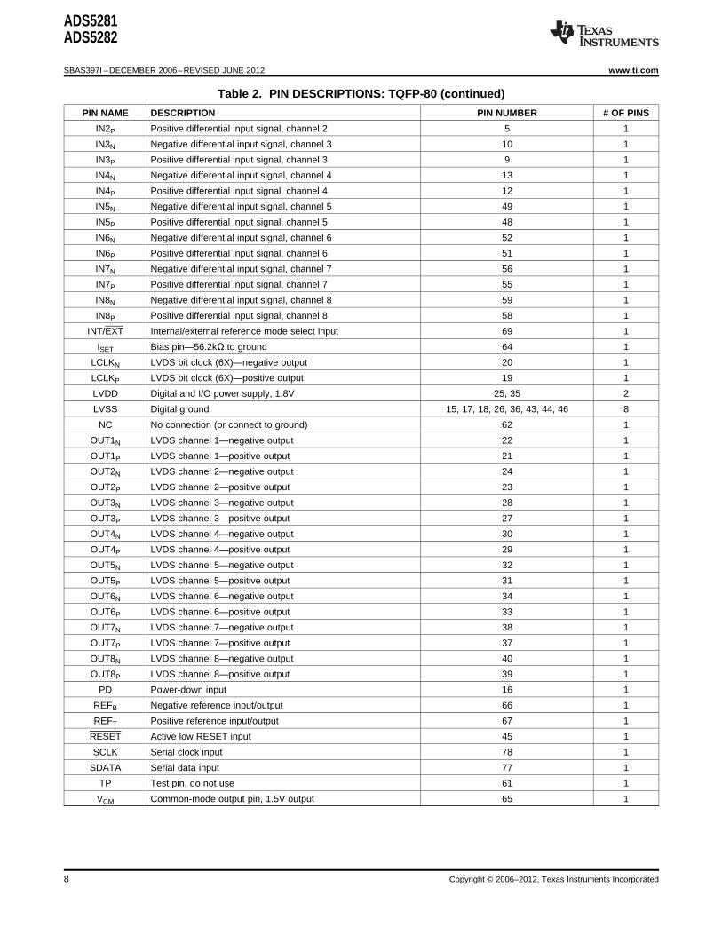
ADS5281ADS5282
SBAS397I ndashDECEMBER 2006ndashREVISED JUNE 2012 wwwticom
Table 2 PIN DESCRIPTIONS TQFP-80 (continued)
PIN NAME DESCRIPTION PIN NUMBER OF PINS
IN2P Positive differential input signal channel 2 5 1
IN3N Negative differential input signal channel 3 10 1
IN3P Positive differential input signal channel 3 9 1
IN4N Negative differential input signal channel 4 13 1
IN4P Positive differential input signal channel 4 12 1
IN5N Negative differential input signal channel 5 49 1
IN5P Positive differential input signal channel 5 48 1
IN6N Negative differential input signal channel 6 52 1
IN6P Positive differential input signal channel 6 51 1
IN7N Negative differential input signal channel 7 56 1
IN7P Positive differential input signal channel 7 55 1
IN8N Negative differential input signal channel 8 59 1
IN8P Positive differential input signal channel 8 58 1
INTEXT Internalexternal reference mode select input 69 1
ISET Bias pinmdash562kΩ to ground 64 1
LCLKN LVDS bit clock (6X)mdashnegative output 20 1
LCLKP LVDS bit clock (6X)mdashpositive output 19 1
LVDD Digital and IO power supply 18V 25 35 2
LVSS Digital ground 15 17 18 26 36 43 44 46 8
NC No connection (or connect to ground) 62 1
OUT1N LVDS channel 1mdashnegative output 22 1
OUT1P LVDS channel 1mdashpositive output 21 1
OUT2N LVDS channel 2mdashnegative output 24 1
OUT2P LVDS channel 2mdashpositive output 23 1
OUT3N LVDS channel 3mdashnegative output 28 1
OUT3P LVDS channel 3mdashpositive output 27 1
OUT4N LVDS channel 4mdashnegative output 30 1
OUT4P LVDS channel 4mdashpositive output 29 1
OUT5N LVDS channel 5mdashnegative output 32 1
OUT5P LVDS channel 5mdashpositive output 31 1
OUT6N LVDS channel 6mdashnegative output 34 1
OUT6P LVDS channel 6mdashpositive output 33 1
OUT7N LVDS channel 7mdashnegative output 38 1
OUT7P LVDS channel 7mdashpositive output 37 1
OUT8N LVDS channel 8mdashnegative output 40 1
OUT8P LVDS channel 8mdashpositive output 39 1
PD Power-down input 16 1
REFB Negative reference inputoutput 66 1
REFT Positive reference inputoutput 67 1
RESET Active low RESET input 45 1
SCLK Serial clock input 78 1
SDATA Serial data input 77 1
TP Test pin do not use 61 1
VCM Common-mode output pin 15V output 65 1
8 Copyright copy 2006ndash2012 Texas Instruments Incorporated
48
47
46
45
44
43
42
41
40
39
38
37
36
35
34
33
IN8N
IN8P
AVSS
IN7N
IN7P
AVSS
IN6N
IN6P
AVSS
IN5N
IN5P
AVSS
LVSS
LVDD
OUT8N
OUT8P
1
2
3
4
5
6
7
8
9
10
11
12
13
14
15
16
IN1P
IN1N
AVSS
IN2P
IN2N
AVSS
IN3P
IN3N
AVSS
IN4P
IN4N
LVSS
PD
LVSS
OUT1P
OUT1N
RE
SE
T
SC
LK
SD
ATA
CS
AV
DD
CLK
N
CLK
P
AV
DD
INT
EX
T
RE
FT
RE
FB
VC
M
TP
I SE
T
AV
DD
AV
DD
OU
T2
P
OU
T2
N
OU
T3
P
OU
T3
N
OU
T4
P
OU
T4
N
AD
CLK
P
AD
CLK
N
LC
LK
P
LC
LK
N
OU
T5
P
OU
T5
N
OU
T6
P
OU
T6
N
OU
T7
P
OU
T7
N
64 63 62 61 60 59 58 57 56 55 54
17 18 19 20 21 22 23 24 25 26 27
53 52 51 50 49
28 29 30 31 32
ADS528X
ADS5281ADS5282
wwwticom SBAS397I ndashDECEMBER 2006ndashREVISED JUNE 2012
QFN-64 PowerPADTOP VIEW
Table 3 PIN DESCRIPTIONS QFN-64
PIN NAME DESCRIPTION PIN NUMBER OF PINS
ADCLKN LVDS frame clock (1X)mdashnegative output 24 1
ADCLKP LVDS frame clock (1X)mdashpositive output 23 1
AVDD Analog power supply 33V 49 50 57 60 4
AVSS Analog ground 3 6 9 37 40 43 46 7
Negative differential clock inputCLKN 59 1Tie CLKN to 0V for a single-ended clock
CLKP Positive differential clock input 58 1
CS Serial enable chip selectmdashactive low digital input 61 1
IN1N Negative differential input signal channel 1 2 1
IN1P Positive differential input signal channel 1 1 1
IN2N Negative differential input signal channel 2 5 1
IN2P Positive differential input signal channel 2 4 1
IN3N Negative differential input signal channel 3 8 1
IN3P Positive differential input signal channel 3 7 1
IN4N Negative differential input signal channel 4 11 1
IN4P Positive differential input signal channel 4 10 1
IN5N Negative differential input signal channel 5 39 1
Copyright copy 2006ndash2012 Texas Instruments Incorporated 9
ADS5281ADS5282
SBAS397I ndashDECEMBER 2006ndashREVISED JUNE 2012 wwwticom
Table 3 PIN DESCRIPTIONS QFN-64 (continued)
PIN NAME DESCRIPTION PIN NUMBER OF PINS
IN5P Positive differential input signal channel 5 38 1
IN6N Negative differential input signal channel 6 42 1
IN6P Positive differential input signal channel 6 41 1
IN7N Negative differential input signal channel 7 45 1
IN7P Positive differential input signal channel 7 44 1
IN8N Negative differential input signal channel 8 48 1
IN8P Positive differential input signal channel 8 47 1
INTEXT Internalexternal reference mode select input 56 1
ISET Bias pinmdash562kΩ to ground 51 1
LCLKN LVDS bit clock (6X)mdashnegative output 26 1
LCLKP LVDS bit clock (6X)mdashpositive output 25 1
LVDD Digital and IO power supply 18V 35 1
LVSS Digital ground 12 14 36 3
OUT1N LVDS channel 1mdashnegative output 16 1
OUT1P LVDS channel 1mdashpositive output 15 1
OUT2N LVDS channel 2mdashnegative output 18 1
OUT2P LVDS channel 2mdashpositive output 17 1
OUT3N LVDS channel 3mdashnegative output 20 1
OUT3P LVDS channel 3mdashpositive output 19 1
OUT4N LVDS channel 4mdashnegative output 22 1
OUT4P LVDS channel 4mdashpositive output 21 1
OUT5N LVDS channel 5mdashnegative output 28 1
OUT5P LVDS channel 5mdashpositive output 27 1
OUT6N LVDS channel 6mdashnegative output 30 1
OUT6P LVDS channel 6mdashpositive output 29 1
OUT7N LVDS channel 7mdashnegative output 32 1
OUT7P LVDS channel 7mdashpositive output 31 1
OUT8N LVDS channel 8mdashnegative output 34 1
OUT8P LVDS channel 8mdashpositive output 33 1
PD Power-down input 13 1
REFB Negative reference inputoutput 54 1
REFT Positive reference inputoutput 55 1
RESET Active low RESET input 64 1
SCLK Serial clock input 63 1
SDATA Serial data input 62 1
TP Test pin do not use 52 1
VCM Common-mode output pin 15V output 53 1
10 Copyright copy 2006ndash2012 Texas Instruments Incorporated
12-BitADC
PLL
Serializer
1x ADCLK
6x ADCLK
IN1P
IN1N
OUT1P
OUT1N
12-BitADC
SerializerIN2P
IN2N
OUT2P
OUT2N
12-BitADC
SerializerIN3P
IN3N
OUT3P
OUT3N
LCLKP
LCLKN
ADCLKP
ADCLKN
12x ADCLK
12-BitADC
SerializerIN4P
IN4N
OUT4P
OUT4N
12-BitADC
SerializerIN5P
IN5N
OUT5P
OUT5N
12-BitADC
SerializerIN6P
IN6N
OUT6P
OUT6N
12-BitADC
SerializerIN7P
IN7N
OUT7P
OUT7N
12-BitADC
Serializer
Digital
Digital
Digital
Digital
Digital
Digital
Digital
Digital
Reference
IN8P
IN8N
RE
FT
INT
EX
T
RE
FB
VC
M
OUT8P
OUT8N
I SE
T
Registers
SD
ATA
CS
RE
SE
T
SC
LK
ADC
Control
PD
Clock
Buffer
(AD
CL
K)
CL
KP
(AV
SS
)
CL
KN
AV
DD
(33
V)
LV
DD
(18
V)
Power-
Down
Te
st
Pa
tte
rns
Drive
Cu
rre
nt
Ou
tpu
t F
orm
at
Dig
ita
l G
ain
(0d
B-1
2d
B)
ADS5281ADS5282
wwwticom SBAS397I ndashDECEMBER 2006ndashREVISED JUNE 2012
FUNCTIONAL BLOCK DIAGRAM
Copyright copy 2006ndash2012 Texas Instruments Incorporated 11
tH1
tSU1
tH2
tSU2
LCLKN
LCLKP
OUTN
OUTP
D0 D1 D2 D3 D4 D5 D6 D7 D8 D9 D10 D11 D0 D1 D2 D3 D4 D5 D6 D7 D8 D9 D10 D11D0 D1 D2 D3 D4 D5 D6 D7 D8 D9 D10 D11
Sample nSample n + 12
tPROP
t (A)D
12 clocks latency
Analog Input
Clock Input
6X ADCLK
LCLKN
LCLKP
1X ADCLK
ADCLKN
ADCLKP
SERIAL DATA
OUTP
OUTN
tSAMPLE
Sample n + 13
ADS5281ADS5282
SBAS397I ndashDECEMBER 2006ndashREVISED JUNE 2012 wwwticom
LVDS TIMING DIAGRAM
DEFINITION OF SETUP AND HOLD TIMES
tSU = min(tSU1 tSU2)
tH = min(tH1 tH2)
TIMING CHARACTERISTICS (1) (2)
ADS528x
PARAMETER TEST CONDITIONS MIN TYP MAX UNIT
tA Aperture delay 15 45 ns
Aperture delay variation Channel-to-channel within the same device (3σ) plusmn20 ps
tJ Aperture jitter 400 fs
Time to valid data after coming out of 50 μsCOMPLETE POWER-DOWN mode
Time to valid data after coming out of PARTIALtWAKE Wake-up time POWER-DOWN mode (with clock continuing to 2 μs
run during power-down)
Time to valid data after stopping and restarting 40 μsthe input clock
ClockData latency 12 cycles
(1) Timing characteristics are common to the ADS528x family(2) Timing parameters are ensured by design and characterization not production tested
12 Copyright copy 2006ndash2012 Texas Instruments Incorporated
ADS5281ADS5282
wwwticom SBAS397I ndashDECEMBER 2006ndashREVISED JUNE 2012
LVDS OUTPUT TIMING CHARACTERISTICS (1) (2)
Typical values are at +25degC minimum and maximum values are measured across the specified temperature range of TMIN = ndash40degC to TMAX =+85degC sampling frequency = as specified CLOAD = 5pF (3) IOUT = 35mA RLOAD = 100Ω (4) and no internal termination unless otherwisenoted
ADS528x
40MSPS 50MSPS 65MSPS
PARAMETER TEST CONDITIONS (5) MIN TYP MAX MIN TYP MAX MIN TYP MAX UNIT
Data valid (7) to zero-crossing oftSU Data setup time(6) 067 047 027 ns
LCLKP
Zero-crossing of LCLKP to datatH Data hold time(6) 085 065 04 ns
becoming invalid(7)
Input clock (ADCLK) rising edgetPROP Clock propagation delay cross-over to output clock (ADCLKP) 10 14 166 10 125 141 97 115 14 ns
rising edge cross-over
Duty cycle of differential clockLVDS bit clock duty cycle 455 50 53 45 50 535 41 50 57
(LCLKP ndash LCLKN)
Bit clock cycle-to-cycle250 250 250 ps pp
jitter
Frame clock cycle-to-cycle150 150 150 ps pp
jitter
tRISE Data rise time data fall Rise time is from ndash100mV to +100mV009 02 04 009 02 04 009 02 04 ns
tFALL time Fall time is from +100mV to ndash100mV
tCLKRISE Output clock rise time Rise time is from ndash100mV to +100mV009 02 04 009 02 04 009 02 04 ns
tCLKFALL output clock fall time Fall time is from +100mV to ndash100mV
(1) All characteristics are at the maximum rated speed for each speed grade(2) Timing parameters are ensured by design and characterization not production tested(3) CLOAD is the effective external single-ended load capacitance between each output pin and ground(4) IOUT refers to the LVDS buffer current setting RLOAD is the differential load resistance between the LVDS output pair(5) Measurements are done with a transmission line of 100Ω characteristic impedance between the device and the load(6) Setup and hold time specifications take into account the effect of jitter on the output data and clock These specifications also assume
that data and clock paths are perfectly matched within the receiver Any mismatch in these paths within the receiver would appear asreduced timing margin
(7) Data valid refers to a logic high of +100mV and a logic low of ndash100mV
LVDS OUTPUT TIMING CHARACTERISTICS (1) (2)
Typical values are at +25degC minimum and maximum values are measured across the specified temperature range of TMIN = ndash40degC to TMAX =+85degC sampling frequency = as specified CLOAD = 5pF (3) IOUT = 35mA RLOAD = 100Ω (4) and no internal termination unless otherwisenoted
ADS528x
30MSPS 20MSPS 10MSPS
PARAMETER TEST CONDITIONS (5) MIN TYP MAX MIN TYP MAX MIN TYP MAX UNIT
Data valid (7) to zero-crossing oftSU Data setup time(6) 08 15 37 ns
LCLKP
Zero-crossing of LCLKP to datatH Data hold time(6) 12 19 39 ns
becoming invalid(7)
Input clock (ADCLK) rising edgetPROP Clock propagation delay cross-over to output clock (ADCLKP) 95 135 173 95 145 173 10 147 171 ns
rising edge cross-over
Duty cycle of differential clockLVDS bit clock duty cycle 465 50 52 48 50 51 49 50 51
(LCLKP ndash LCLKN)
Bit clock cycle-to-cycle250 250 750 ps pp
jitter
Frame clock cycle-to-cycle150 150 500 ps pp
jitter
tRISE Data rise time data fall Rise time is from ndash100mV to +100mV009 02 04 009 02 04 009 02 04 ns
tFALL time Fall time is from +100mV to ndash100mV
tCLKRISE Output clock rise time Rise time is from ndash100mV to +100mV009 02 04 009 02 04 009 02 04 ns
tCLKFALL output clock fall time Fall time is from +100mV to ndash100mV
(1) All characteristics are at the speeds other than the maximum rated speed for each speed grade(2) Timing parameters are ensured by design and characterization not production tested(3) CLOAD is the effective external single-ended load capacitance between each output pin and ground(4) IOUT refers to the LVDS buffer current setting RLOAD is the differential load resistance between the LVDS output pair(5) Measurements are done with a transmission line of 100Ω characteristic impedance between the device and the load(6) Setup and hold time specifications take into account the effect of jitter on the output data and clock These specifications also assume
that data and clock paths are perfectly matched within the receiver Any mismatch in these paths within the receiver would appear asreduced timing margin
(7) Data valid refers to a logic high of +100mV and a logic low of ndash100mV
Copyright copy 2006ndash2012 Texas Instruments Incorporated 13
t1
t2
t3
AVDD (3V to 36V)
LVDD (17V to 19V)
High-Level RESET
(14V to 36V)
High-Level CS
(14V to 36V)
Device Ready for
Serial Register Write(2)
Device Ready for
Data ConversionStart of Clock
AVDD
LVDD
RESET
CS
ADCLK
t4 t7
t5
t8
t6
ADS5281ADS5282
SBAS397I ndashDECEMBER 2006ndashREVISED JUNE 2012 wwwticom
LVDS OUTPUT TIMING CHARACTERISTICSTIMINGS WHEN USING REGISTER 0xE3 (2)
At 40 MSPSPARAMETER (1) TEST CONDITIONS
MIN TYP MAX
Data setup time Data valid (3) to zero-crossing of LCLKp 060
Data hold time Zero-crossing of LCLKP to data becoming invalid(3) 092
Input clock (ADCLK) rising edge cross-over to output clock (ADCLK) rising edgeClock propagation delay 8 12 146
crossover
(1) Only the setup time hold time and clock propagation delay parameters are affected Rest of the parameters are same as given inprevious two tables
(2) Only timing specifications for 40MSPS are affected when using register 0xE3 (as specified in the recommended operating table section)The timing specifications for other clock frequencies are same as given in previous two tables
(3) Data valid refers to logic high of +100mV and logic low of ndash100mV
RECOMMENDED POWER-UP SEQUENCING AND RESET TIMING
10μs lt t1 lt 50ms 10μs lt t2 lt 50ms ndash10ms lt t3 lt 10ms t4 gt 10ms t5 gt 100ns t6 gt 100ns t7 gt 10ms and t8 gt 100μs
(1) The AVDD and LVDD power on sequence does not matter as long as ndash10ms lt t3 lt 10ms Similar considerations apply while shuttingdown the device
(2) Write initialization registers listed in the Initialization Registers table
14 Copyright copy 2006ndash2012 Texas Instruments Incorporated
PD
Device Fully
Powers DownDevice Fully
Powers Up
tWAKE1 sm
ADS5281ADS5282
wwwticom SBAS397I ndashDECEMBER 2006ndashREVISED JUNE 2012
POWER-DOWN TIMING
Power-up time shown is based on 1μF bypass capacitors on the reference pins tWAKE is the time it takes for the device to wake upcompletely from power-down mode The ADS528x has two power-down modes complete power-down mode and partial power-down modeThe device can be configured in partial power-down mode through a register setting
tWAKE lt 50μs for complete power-down mode
tWAKE lt 2μs for partial power-down mode (provided the clock is not shut off during power-down)
Copyright copy 2006ndash2012 Texas Instruments Incorporated 15
D15 D14 D13 D12 D11 D10 D9 D8 D7 D6 D5 D4 D3 D2 D1 D0A7 A6 A5 A4 A3 A2 A1 A0
CS
SCLK
SDATA
Data latched on rising edge of SCLK
Start Sequence End Sequence
t6
t4
t2
t7
t3
t5
t1
ADS5281ADS5282
SBAS397I ndashDECEMBER 2006ndashREVISED JUNE 2012 wwwticom
SERIAL INTERFACE
The ADS528x has a set of internal registers that can be accessed through the serial interface formed by pins CS(chip select active low) SCLK (serial interface clock) and SDATA (serial interface data) When CS is low thefollowing actions occurbull Serial shift of bits into the device is enabledbull SDATA (serial data) is latched at every rising edge of SCLKbull SDATA is loaded into the register at every 24th SCLK rising edge
If the word length exceeds a multiple of 24 bits the excess bits are ignored Data can be loaded in multiples of24-bit words within a single active CS pulse The first eight bits form the register address and the remaining 16bits form the register data The interface can work with SCLK frequencies from 20MHz down to very low speeds(a few hertz) and also with a non-50 SCLK duty cycle
Register Initialization
After power-up the internal registers must be initialized to the respective default values Initialization can bedone in one of two ways1 Through a hardware reset by applying a low-going pulse on the RESET pin or2 Through a software reset using the serial interface set the RST bit high Setting this bit initializes the
internal registers to the respective default values and then self-resets the RST bit low In this case theRESET pin stays high (inactive)
After all registers have been initialized to their default values through a RESET operation the registers detailedin the Initialization Registers table must be written into This process must be done after every hardware orsoftware RESET operation in order to reconfigure the device for the best mode of operation
SERIAL INTERFACE TIMING
ADS528x
PARAMETER DESCRIPTION MIN TYP MAX UNIT
t1 SCLK period 50 ns
t2 SCLK high time 20 ns
t3 SCLK low time 20 ns
t4 Data setup time 5 ns
t5 Data hold time 5 ns
t6 CS fall to SCLK rise 8 ns
t7 Time between last SCLK rising edge to CS rising edge 8 ns
16 Copyright copy 2006ndash2012 Texas Instruments Incorporated
ADS5281ADS5282
wwwticom SBAS397I ndashDECEMBER 2006ndashREVISED JUNE 2012
SERIAL REGISTER MAP
Table 4 SUMMARY OF FUNCTIONS SUPPORTED BY SERIAL INTERFACE (1) (2) (3) (4)
ADDRESSIN HEX D15 D14 D13 D12 D11 D10 D9 D8 D7 D6 D5 D4 D3 D2 D1 D0 NAME DESCRIPTION DEFAULT
00 X RST Self-clearing software RESET Inactive
Channel-specific ADC power-X X X X X X X X PDN_CHlt81gt Inactive
down mode
Partial power-down mode (fastX PDN_PARTIAL Inactive
recovery from power-down)0F
Register mode for completeX PDN_COMPLETE Inactive
power-down (slower recovery)
Configures the PD pin for partial CompleteX PDN_PIN_CFG
power-down mode power-down
LVDS current driveX X X ILVDS_LCLKlt20gt programmability for LCLKN and 35mA drive
LCLKP pins
LVDS current driveILVDS_FRAME
11 X X X programmability for ADCLKN and 35mA drivelt20gt
ADCLKP pins
LVDS current driveX X X ILVDS_DATlt20gt programmability for OUTN and 35mA drive
OUTP pins
Enables internal termination for TerminationX EN_LVDS_TERM
LVDS buffers disabled
Programmable termination for Termination1 X X X TERM_LCLKlt20gt
LCLKN and LCLKP buffers disabled12
TERM_FRAME Programmable termination for Termination1 X X X
lt20gt ADCLKN and ADCLKP buffers disabled
Programmable termination for Termination1 X X X TERM_DATlt20gt
OUTN and OUTP buffers disabled
Channel-specific low-frequency14 X X X X X X X X LFNS_CHlt81gt Inactive
noise suppression mode enable
INP isSwaps the polarity of the analog
24 X X X X X X X X INVERT_CHlt81gt positiveinput pins electrically
input
Enables a repeating full-scaleX 0 0 EN_RAMP Inactive
ramp pattern on the outputs
Enables the mode wherein theDUALCUSTOM_
0 X 0 output toggles between two InactivePAT
defined codes
Enables the mode wherein theSINGLE_CUSTOM
0 0 X output is a constant specified Inactive25 _PAT
code
2MSBs for a single customBITS_CUSTOM1 pattern (and for the first code of
X X Inactivelt1110gt the dual custom pattern) lt11gt is
the MSB
BITS_CUSTOM2 2MSBs for the second code ofX X Inactive
lt1110gt the dual custom pattern
10 lower bits for the singleBITS_CUSTOM1 custom pattern (and for the first
26 X X X X X X X X X X Inactivelt90gt code of the dual custom pattern)
lt0gt is the LSB
BITS_CUSTOM2 10 lower bits for the second27 X X X X X X X X X X Inactive
lt90gt code of the dual custom pattern
X X X X GAIN_CH1lt30gt Programmable gain channel 1 0dB gain
X X X X GAIN_CH2lt30gt Programmable gain channel 2 0dB gain2A
X X X X GAIN_CH3lt30gt Programmable gain channel 3 0dB gain
X X X X GAIN_CH4lt30gt Programmable gain channel 4 0dB gain
X X X X GAIN_CH5lt30gt Programmable gain channel 5 0dB gain
X X X X GAIN_CH6lt30gt Programmable gain channel 6 0dB gain2B
X X X X GAIN_CH7lt30gt Programmable gain channel 7 0dB gain
X X X X GAIN_CH8lt30gt Programmable gain channel 8 0dB gain
(1) The unused bits in each register (identified as blank table cells) must be programmed as 0(2) X = Register bit referenced by the corresponding name and description (default is 0)(3) Bits marked as 0 should be forced to 0 and bits marked as 1 should be forced to 1 when the particular register is programmed(4) Multiple functions in a register should be programmed in a single write operation
Copyright copy 2006ndash2012 Texas Instruments Incorporated 17
ADS5281ADS5282
SBAS397I ndashDECEMBER 2006ndashREVISED JUNE 2012 wwwticom
Table 4 SUMMARY OF FUNCTIONS SUPPORTED BY SERIAL INTERFACE(1) (2) (3) (4) (continued)ADDRESS
IN HEX D15 D14 D13 D12 D11 D10 D9 D8 D7 D6 D5 D4 D3 D2 D1 D0 NAME DESCRIPTION DEFAULT
Single-1 X DIFF_CLK Differential clock mode
ended clock
Enables the duty-cycle correction1 X EN_DCC Disabled
circuit
External42Drives the external reference reference
1 X EXT_REF_VCMmode through the VCM pin drives REFT
and REFB
Controls the phase of LCLK1 X X PHASE_DDRlt10gt 90 degrees
output relative to data
0 X PAT_DESKEW Enables deskew pattern mode Inactive45
X 0 PAT_SYNC Enables sync pattern mode Inactive
Binary twos complement format Straight1 1 X BTC_MODE
for ADC output offset binary
Serialized ADC output comes LSB-first1 1 X MSB_FIRST
out MSB-first output
Enables SDR output modeDDR output46 1 1 X EN_SDR (LCLK becomes a 12x input
modeclock)
Controls whether the LCLK rising Rising edgeor falling edge comes in the of LCLK in
1 X 1 1 FALL_SDRmiddle of the data window when middle ofoperating in SDR output mode data window
SUMMARY OF FEATURES
POWER IMPACT (relative to default)FEATURES DEFAULT SELECTION AT fS = 65MSPS
ANALOG FEATURES
Internal or external reference Internal reference mode uses approximately 23mW moreNA Pin(driven on the REFT and REFB pins) power on AVDD
External reference driven on the Off Register 42 Approximately 9mW less power on AVDDVCM pin
Duty cycle correction circuit Off Register 42 Approximately 7mW more power on AVDD
With zero input to the ADC low-frequency noise suppressionLow-frequency noise suppression Off Register 14 causes digital switching at fS2 thereby increasing LVDD
power by approximately 7mWchannel
Differential clock mode uses approximately 7mW more powerSingle-ended or differential clock Single-ended Register 42 on AVDD
Refer to the Power-Down Modes section in the ElectricalPower-down mode Off Pin and register 0F Characteristics table
DIGITAL FEATURES
Programmable digital gain (0dB to Registers 2A and0dB No difference12dB) 2B
Straight offset or BTC output Straight offset Register 46 No difference
Swap polarity of analog input pins Off Register 24 No difference
LVDS OUTPUT PHYSICAL LAYER
LVDS internal termination Off Register 12 Approximately 7mW more power on AVDD
LVDS current programmability 35mA Register 11 As per LVDS clock and data buffer current setting
LVDS OUTPUT TIMING
LSB- or MSB-first output LSB-first Register 46 No difference
SDR mode uses approximately 2mW more power on LVDDDDR or SDR output DDR Register 46 (at fS = 30MSPS)
Refer toLCLK phase relative to data output Register 42 No differenceFigure 1
18 Copyright copy 2006ndash2012 Texas Instruments Incorporated
ADS5281ADS5282
wwwticom SBAS397I ndashDECEMBER 2006ndashREVISED JUNE 2012
DESCRIPTION OF SERIAL REGISTERS
SOFTWARE RESET
ADDRESSIN HEX D15 D14 D13 D12 D11 D10 D9 D8 D7 D6 D5 D4 D3 D2 D1 D0 NAME
00 X RST
Software reset is applied when the RST bit is set to 1 setting this bit resets all internal registers and self-clearsto 0
POWER-DOWN MODES
ADDRESSIN HEX D15 D14 D13 D12 D11 D10 D9 D8 D7 D6 D5 D4 D3 D2 D1 D0 NAME
X X X X X X X X PDN_CHlt81gt
X PDN_PARTIAL0F
0 X PDN_COMPLETE
X 0 PDN_PIN_CFG
Each of the eight channels can be individually powered down PDN_CHltNgt controls the power-down mode forthe ADC channel ltNgt
In addition to channel-specific power-down the ADS528x also has two global power-down modesmdashpartialpower-down mode and complete power-down mode Partial power-down mode partially powers down the chiprecovery from this mode is much quicker provided that the clock has been running for at least 50μs beforeexiting this mode Complete power-down mode on the other hand completely powers down the chip andinvolves a much longer recovery time
In addition to programming the device for either of these two power-down modes (through either thePDN_PARTIAL or PDN_COMPLETE bits respectively) the PD pin itself can be configured as either a partialpower-down pin or a complete power-down pin control For example if PDN_PIN_CFG = 0 (default) when thePD pin is high the device enters complete power-down mode However if PDN_PIN_CFG = 1 when the PD pinis high the device enters partial power-down mode
LVDS DRIVE PROGRAMMABILITY
ADDRESSIN HEX D15 D14 D13 D12 D11 D10 D9 D8 D7 D6 D5 D4 D3 D2 D1 D0 NAME
X X X ILVDS_LCLKlt20gt
11 X X X ILVDS_FRAMElt20gt
X X X ILVDS_DATlt20gt
The LVDS drive strength of the bit clock (LCLKP or LCLKN) and the frame clock (ADCLKP or ADCLKN) can beindividually programmed The LVDS drive strengths of all the data outputs OUTP and OUTN can also beprogrammed to the same value
Copyright copy 2006ndash2012 Texas Instruments Incorporated 19
ADS5281ADS5282
SBAS397I ndashDECEMBER 2006ndashREVISED JUNE 2012 wwwticom
All three drive strengths (bit clock frame clock and data) are programmed using sets of three bits Table 5shows an example of how the drive strength of the bit clock is programmed (the method is similar for the frameclock and data drive strengths)
Table 5 Bit Clock Drive Strength (1)
ILVDS_LCLKlt2gt ILVDS_LCLKlt1gt ILVDS_LCLKlt0gt LVDS DRIVE STRENGTH FOR LCLKP AND LCLKN
0 0 0 35mA (default)
0 0 1 25mA
0 1 0 15mA
0 1 1 05mA
1 0 0 75mA
1 0 1 65mA
1 1 0 55mA
1 1 1 45mA
(1) Current settings lower than 15mA are not recommended
LVDS INTERNAL TERMINATION PROGRAMMABILITY
ADDRESSIN HEX D15 D14 D13 D12 D11 D10 D9 D8 D7 D6 D5 D4 D3 D2 D1 D0 NAME
X EN_LVDS_TERM
1 X X X TERM_LCLKlt20gt12
1 X X X TERM_FRAMElt20gt
1 X X X TERM_DATlt20gt
The LVDS buffers have high-impedance current sources driving the outputs When driving traces whosecharacteristic impedance is not perfectly matched with the termination impedance on the receiver side there maybe reflections back to the LVDS output pins of the ADS528x that cause degraded signal integrity By enabling aninternal termination (between the positive and negative outputs) for the LVDS buffers the signal integrity can besignificantly improved in such scenarios To set the internal termination mode the EN_LVDS_TERM bit shouldbe set to 1 Once this bit is set the internal termination values for the bit clock frame clock and data bufferscan be independently programmed using sets of three bits Table 6 shows an example of how the internaltermination of the LVDS buffer driving the bit clock is programmed (the method is similar for the frame clock anddata buffers) These termination values are only typical values and can vary by up to plusmn20 across temperatureand from device to device
Table 6 Bit Clock Internal Termination
INTERNAL TERMINATION BETWEENTERM_LCLKlt2gt TERM_LCLKlt1gt TERM_LCLKlt0gt LCLKP AND LCLKN IN Ω
0 0 0 None
0 0 1 260
0 1 0 150
0 1 1 94
1 0 0 125
1 0 1 80
1 1 0 66
1 1 1 55
20 Copyright copy 2006ndash2012 Texas Instruments Incorporated
ADS5281ADS5282
wwwticom SBAS397I ndashDECEMBER 2006ndashREVISED JUNE 2012
LOW-FREQUENCY NOISE SUPPRESSION MODE
ADDRESSIN HEX D15 D14 D13 D12 D11 D10 D9 D8 D7 D6 D5 D4 D3 D2 D1 D0 NAME
14 X X X X X X X X LFNS_CHlt81gt
The low-frequency noise suppression mode is specifically useful in applications where good noise performance isdesired in the frequency band of 0MHz to 1MHz (around dc) Setting this mode shifts the low-frequency noise ofthe ADS528x to approximately fS2 thereby moving the noise floor around dc to a much lower valueLFNS_CHlt81gt enables this mode individually for each channel
ANALOG INPUT INVERT
ADDRESSIN HEX D15 D14 D13 D12 D11 D10 D9 D8 D7 D6 D5 D4 D3 D2 D1 D0 NAME
24 X X X X X X X X INVERT_CHlt81gt
Normally the INP pin represents the positive analog input pin and INN represents the complementary negativeinput Setting the bits marked INVERT_CHlt81gt (individual control for each channel) causes the inputs to beswapped INN now represents the positive input and INP the negative input
LVDS TEST PATTERNS
ADDRESSIN HEX D15 D14 D13 D12 D11 D10 D9 D8 D7 D6 D5 D4 D3 D2 D1 D0 NAME
X 0 0 EN_RAMP
0 X 0 DUALCUSTOM_PAT
25 0 0 X SINGLE_CUSTOM_PAT
X X BITS_CUSTOM1lt1110gt
X X BITS_CUSTOM2lt1110gt
26 X X X X X X X X X X BITS_CUSTOM1lt90gt
27 X X X X X X X X X X BITS_CUSTOM2lt90gt
0 X PAT_DESKEW45
X 0 PAT_SYNC
The ADS528x can output a variety of test patterns on the LVDS outputs These test patterns replace the normalADC data output Setting EN_RAMP to 1 causes all the channels to output a repeating full-scale ramp patternThe ramp increments from zero code to full-scale code in steps of 1LSB every clock cycle After hitting the full-scale code it returns back to zero code and ramps again
The device can also be programmed to output a constant code by setting SINGLE_CUSTOM_PAT to 1 andprogramming the desired code in BITS_CUSTOM1lt110gt In this mode BITS_CUSTOM1lt110gt take the placeof the 12-bit ADC data at the output and are controlled by LSB-first and MSB-first modes in the same way asnormal ADC data are
The device may also be made to toggle between two consecutive codes by programming DUAL_CUSTOM_PATto 1 The two codes are represented by the contents of BITS_CUSTOM1lt110gt and BITS_CUSTOM2lt110gt
In addition to custom patterns the device may also be made to output two preset patterns1 Deskew patten Set using PAT_DESKEW this mode replaces the 12-bit ADC output Dlt110gt with the
010101010101 word2 Sync pattern Set using PAT_SYNC the normal ADC word is replaced by a fixed 111111000000 word
Note that only one of the above patterns should be active at any given instant
Copyright copy 2006ndash2012 Texas Instruments Incorporated 21
ADS5281ADS5282
SBAS397I ndashDECEMBER 2006ndashREVISED JUNE 2012 wwwticom
PROGRAMMABLE GAIN
ADDRESSIN HEX D15 D14 D13 D12 D11 D10 D9 D8 D7 D6 D5 D4 D3 D2 D1 D0 NAME
X X X X GAIN_CH1lt30gt
X X X X GAIN_CH2lt30gt2A
X X X X GAIN_CH3lt30gt
X X X X GAIN_CH4lt30gt
X X X X GAIN_CH5lt30gt
X X X X GAIN_CH6lt30gt2B
X X X X GAIN_CH7lt30gt
X X X X GAIN_CH8lt30gt
In applications where the full-scale swing of the analog input signal is much less than the 2VPP range supportedby the ADS528x a programmable gain can be set to achieve the full-scale output code even with a lower analoginput swing The programmable gain not only fills the output code range of the ADC but also enhances the SNRof the device by utilizing quantization information from some extra internal bits The programmable gain for eachchannel can be individually set using a set of four bits indicated as GAIN_CHNlt30gt for Channel N The gainsetting is coded in binary from 0dB to 12dB as shown in Table 7
Table 7 Gain Setting for Channel 1
GAIN_CH1lt3gt GAIN_CH1lt2gt GAIN_CH1lt1gt GAIN_CH1lt0gt CHANNEL 1 GAIN SETTING
0 0 0 0 0dB
0 0 0 1 1dB
0 0 1 0 2dB
0 0 1 1 3dB
0 1 0 0 4dB
0 1 0 1 5dB
0 1 1 0 6dB
0 1 1 1 7dB
1 0 0 0 8dB
1 0 0 1 9dB
1 0 1 0 10dB
1 0 1 1 11dB
1 1 0 0 12dB
1 1 0 1 Do not use
1 1 1 0 Do not use
1 1 1 1 Do not use
22 Copyright copy 2006ndash2012 Texas Instruments Incorporated
VREF = 15V -B
VCM
15V
VREF = 15V +T
VCM
15V
ADS5281ADS5282
wwwticom SBAS397I ndashDECEMBER 2006ndashREVISED JUNE 2012
CLOCK REFERENCE AND DATA OUTPUT MODES
ADDRESSIN HEX D15 D14 D13 D12 D11 D10 D9 D8 D7 D6 D5 D4 D3 D2 D1 D0 NAME
1 X DIFF_CLK
1 X EN_DCC42
1 X EXT_REF_VCM
1 X X PHASE_DDRlt10gt
1 1 X BTC_MODE
1 1 X MSB_FIRST46
1 1 X EN_SDR
1 X 1 1 FALL_SDR
INPUT CLOCK
The ADS528x is configured by default to operate with a single-ended input clockmdashCLKP is driven by a CMOSclock and CLKN is tied to 0 However by programming DIFF_CLK to 1 the device can be made to work with adifferential input clock on CLKP and CLKN Operating with a low-jitter differential clock usually gives better SNRperformance especially at input frequencies greater than 30MHz
In cases where the duty cycle of the input clock falls outside the 45 to 55 range it is recommended to enablean internal duty cycle correction circuit This enabling is done by setting the EN_DCC bit to 1
EXTERNAL REFERENCE
The ADS528x can be made to operate in external reference mode by pulling the INTEXT pin to 0 In this modethe REFT and REFB pins should be driven with voltage levels of 25V and 05V respectively and must haveenough drive strength to drive the switched capacitance loading of the reference voltages by each ADC Theadvantage of using the external reference mode is that multiple ADS528x units can be made to operate with thesame external reference thereby improving parameters such as gain matching across devices However inapplications that do not have an available high drive differential external reference the ADS528x can still bedriven with a single external reference voltage on the VCM pin When EXT_REF_VCM is set as 1 (and theINTEXT pin is set to 0) the VCM pin is configured as an input pin and the voltages on REFT and REFB aregenerated as shown in Equation 1 and Equation 2
(1)
(2)
Copyright copy 2006ndash2012 Texas Instruments Incorporated 23
PHASE_DDRlt10gt = 00
PHASE_DDRlt10gt = 01
PHASE_DDRlt10gt = 10
PHASE_DDRlt10gt = 11
ADCLKP
LCLKP
OUTP
ADCLKP
LCLKP
OUTP
ADCLKP
LCLKP
OUTP
ADCLKP
LCLKP
OUTP
ADCLKP
LCLKP
OUTP
ADS5281ADS5282
SBAS397I ndashDECEMBER 2006ndashREVISED JUNE 2012 wwwticom
BIT CLOCK PROGRAMMABILITY
The output interface of the ADS528x is normally a DDR interface with the LCLK rising edge and falling edgetransitions in the middle of alternate data windows This default phase is shown in Figure 1
Figure 1 Default Phase of LCLK
The phase of LCLK can be programmed relative to the output frame clock and data using bitsPHASE_DDRlt10gt The LCLK phase modes are shown in Figure 2
Figure 2 Phase Programmability Modes for LCLK
24 Copyright copy 2006ndash2012 Texas Instruments Incorporated
EN_SDR = 1 FALL_SDR = 0
EN_SDR = 1 FALL_SDR = 1
ADCLKP
LCLKP
OUTP
ADCLKP
LCLKP
OUTP
ADS5281ADS5282
wwwticom SBAS397I ndashDECEMBER 2006ndashREVISED JUNE 2012
In addition to programming the phase of LCLK in the DDR mode the device can also be made to operate in SDRmode by setting the EN_SDR bit to 1 In this mode the bit clock (LCLK) is output at 12x times the input clock ortwice the rate as in DDR mode Depending on the state of FALL_SDR LCLK may be output in either of the twomanners shown in Figure 3 As can be seen in Figure 3 only the LCLK rising (or falling) edge is used to capturethe output data in SDR mode
Figure 3 SDR Interface Modes
The SDR mode does not work well beyond 40MSPS because the LCLK frequency becomes very high
DATA OUTPUT FORMAT MODES
The ADC output by default is in straight offset binary mode Programming the BTC_MODE bit to 1 inverts theMSB and the output becomes binary twos complement mode
Also by default the first bit of the frame (following the rising edge of ADCLKP) is the LSB of the ADC outputProgramming the MSB_FIRST mode inverts the bit order in the word and the MSB is output as the first bitfollowing the ADCLKP rising edge
Copyright copy 2006ndash2012 Texas Instruments Incorporated 25
0
-
-
-
-
-
-
-
-
-
20
40
60
80
100
120
140
160
180
Input Frequency (MHz)
0 25
Am
plit
ude (
dB
)
2015105
SFDR = 884dBc
SNR = 709dBFS
SINAD = 708dBFS
THD = 875dBc
0
-
-
-
-
-
-
-
-
-
20
40
60
80
100
120
140
160
180
Input Frequency (MHz)
0 25
Am
plit
ude (
dB
)
2015105
SFDR = 856dBc
SNR = 705dBFS
SINAD = 704dBFS
THD = 839dBc
0
-
-
-
-
-
-
-
-
-
20
40
60
80
100
120
140
160
180
Input Frequency (MHz)
0 2 20
Am
plit
ude (
dB
)
1816141210864
SFDR = 853dBc
SNR = 708dBFS
SINAD = 707dBFS
THD = 893dBc
0
-
-
-
-
-
-
-
-
-
20
40
60
80
100
120
140
160
180
Input Frequency (MHz)
0 2 20
Am
plit
ude (
dB
)
1816141210864
SFDR = 828dBc
SNR = 702dBFS
SINAD = 70dBFS
THD = 823dBc
ADS5281ADS5282
SBAS397I ndashDECEMBER 2006ndashREVISED JUNE 2012 wwwticom
TYPICAL CHARACTERISTICSAt TA = +25degC AVDD = +33V LVDD = 18V clock frequency = 65MSPS differential clock mode 1VPP clock amplitude 50
clock duty cycle input frequency = 10MHz ndash1dBFS differential analog input 0dB digital gain setting 15V analog inputcommon-mode low-frequency noise suppression = off internal reference mode ISET resistor = 562kΩ and LVDS buffer
current setting = 35mA unless otherwise noted
SPECTRAL PERFORMANCE SPECTRAL PERFORMANCE(fS = 40MHz fIN = 10MHz) (fS = 40MHz fIN = 25MHz)
Figure 4 Figure 5
SPECTRAL PERFORMANCE SPECTRAL PERFORMANCE(fS = 50MHz fIN = 10MHz) (fS = 50MHz fIN = 25MHz)
Figure 6 Figure 7
26 Copyright copy 2006ndash2012 Texas Instruments Incorporated
0
-20
-40
-60
-80
-100
-120
-140
-180
Input Frequency (MHz)
0 33
Am
plit
ude (
dB
)
2015105
-160
SFDR = 862dBc
SNR = 705dBFS
SNR (0MHz to 1MHz) = 861dBFS
SINAD = 704dBFS
THD = 854dBc
25 30
92
87
82
77
72
67
Input Frequency (MHz)
5 30
Dynam
ic P
erf
orm
ance (
SN
R S
FD
R)
201510 25
SNR (dBFS)
SFDR (dBc)
f = 40MHzS
0
-
-
-
-
-
-
-
-
-
20
40
60
80
100
120
140
160
180
Input Frequency (MHz)
0 33
Am
plit
ude (
dB
)
2015105 25 30
SFDR = 909dBc
SNR = 708dBFS
SINAD = 707dBFS
THD = 904dBc
0
-20
-40
-60
-80
-100
-120
-140
-180
Input Frequency (MHz)
0 33
Am
plit
ude (
dB
)
2015105
-160
SFDR = 874dBc
SNR = 704dBFS
SNR (0MHz to 1MHz) = 819dBFS
SINAD = 703dBFS
THD = 864dBc
25 30
ADS5281ADS5282
wwwticom SBAS397I ndashDECEMBER 2006ndashREVISED JUNE 2012
TYPICAL CHARACTERISTICS (continued)At TA = +25degC AVDD = +33V LVDD = 18V clock frequency = 65MSPS differential clock mode 1VPP clock amplitude 50clock duty cycle input frequency = 10MHz ndash1dBFS differential analog input 0dB digital gain setting 15V analog inputcommon-mode low-frequency noise suppression = off internal reference mode ISET resistor = 562kΩ and LVDS buffercurrent setting = 35mA unless otherwise noted
SPECTRAL PERFORMANCE SPECTRAL PERFORMANCE(fS = 65MHz fIN = 10MHz) (fS = 65MHz fIN = 25MHz)
Figure 8 Figure 9
SPECTRAL PERFORMANCE LOW-FREQUENCY NOISESUPPRESSION MODE ENABLED
(fS = 65MHz fIN = 25MHz) DYNAMIC PERFORMANCE vs INPUT FREQUENCY
Figure 10 Figure 11
Copyright copy 2006ndash2012 Texas Instruments Incorporated 27
95
85
75
65
55
45
35
25
Input Amplitude (dBFS)
Dyn
am
ic P
erf
orm
an
ce
(S
NR
S
FD
R)
SNR (dBFS)
SFDR (dBc)
f = 65MHz
f = 10MHzS
IN
-60 0-50 -40 -30 -20 -10
94
89
84
79
74
69
Clock Amplitude (V Differential)PP
06 23
Dynam
ic P
erf
orm
ance (
SN
R S
FD
R)
1611
SNR (dBFS)
SFDR (dBc)
f = 65MHz
f = 10MHzS
IN
21
95
90
85
80
75
70
65
60
Digital Gain (dB)
0 12
Dyn
am
ic P
erf
orm
an
ce
(S
NR
S
FD
R)
642 8
SNR (dBFS)
SFDR (dBc)
f = 65MHz
f = 10MHzS
IN
10
95
90
85
80
75
70
65
60
AVDD (V)
30 36
Dynam
ic P
erf
orm
ance (
SN
R S
FD
R)
333231 34
SNR (dBFS)
SFDR (dBc)
f = 65MHz
f = 10MHzS
IN
35
92
87
82
77
72
67
Input Frequency (MHz)
5 30
Dynam
ic P
erf
orm
ance (
SN
R S
FD
R)
201510 25
SNR (dBFS)
SFDR (dBc)
f = 50MHzS
97
92
87
82
77
72
67
Input Frequency (MHz)
5 30
Dynam
ic P
erf
orm
ance (
SN
R S
FD
R)
201510 25
SNR (dBFS)
SFDR (dBc)
f = 65MHzS
ADS5281ADS5282
SBAS397I ndashDECEMBER 2006ndashREVISED JUNE 2012 wwwticom
TYPICAL CHARACTERISTICS (continued)At TA = +25degC AVDD = +33V LVDD = 18V clock frequency = 65MSPS differential clock mode 1VPP clock amplitude 50clock duty cycle input frequency = 10MHz ndash1dBFS differential analog input 0dB digital gain setting 15V analog inputcommon-mode low-frequency noise suppression = off internal reference mode ISET resistor = 562kΩ and LVDS buffercurrent setting = 35mA unless otherwise noted
DYNAMIC PERFORMANCE vs INPUT FREQUENCY DYNAMIC PERFORMANCE vs INPUT FREQUENCY
Figure 12 Figure 13
DYNAMIC PERFORMANCE vs DIGITAL GAIN DYNAMIC PERFORMANCE vs AVDD
Figure 14 Figure 15
DYNAMIC PERFORMANCE vs INPUT AMPLITUDE DYNAMIC PERFORMANCE vs CLOCK AMPLITUDE
Figure 16 Figure 17
28 Copyright copy 2006ndash2012 Texas Instruments Incorporated
94
89
84
79
74
69
External Reference Common-Mode Voltage (REF + REF )2 (V)T B
135 165
Dynam
ic P
erf
orm
ance (
SN
R S
FD
R)
150145140
SNR (dBFS)
SFDR (dBc)
f = 65MHz
f = 10MHzS
IN
155 160
External reference differential voltage maintained at 2V
94
89
84
79
74
69
Voltage on V (V)CM
135 165
Dynam
ic P
erf
orm
ance (
SN
R S
FD
R)
150145140
SNR (dBFS)
SFDR (dBc)
f = 65MHz
f = 10MHzS
IN
155 160
94
89
84
79
74
69
Analog Input Common-Mode Voltage (V)
130 170
Dynam
ic P
erf
orm
ance (
SN
R S
FD
R)
140135
SNR (dBFS)
SFDR (dBc)
f = 65MHz
f = 10MHzS
IN
145 165160155150
94
89
84
79
74
69
External Reference Differential Voltage REF REF (V)-T B
16 24
Dynam
ic P
erf
orm
ance (
SN
R S
FD
R)
191817
SNR (dBFS)
SFDR (dBc)
f = 65MHz
f = 10MHzS
IN
20 232221
External reference common-mode voltage
maintained at 15V
ADS5281ADS5282
wwwticom SBAS397I ndashDECEMBER 2006ndashREVISED JUNE 2012
TYPICAL CHARACTERISTICS (continued)At TA = +25degC AVDD = +33V LVDD = 18V clock frequency = 65MSPS differential clock mode 1VPP clock amplitude 50clock duty cycle input frequency = 10MHz ndash1dBFS differential analog input 0dB digital gain setting 15V analog inputcommon-mode low-frequency noise suppression = off internal reference mode ISET resistor = 562kΩ and LVDS buffercurrent setting = 35mA unless otherwise noted
DYNAMIC PERFORMANCE vs ANALOG INPUT COMMON- DYNAMIC PERFORMANCE vs EXTERNAL REFERENCEMODE VOLTAGE DIFFERENTIAL VOLTAGE
Figure 18 Figure 19
DYNAMIC PERFORMANCE vs EXTERNAL REFERENCE DYNAMIC PERFORMANCE vs EXTERNAL REFERENCECOMMON-MODE VOLTAGE FORCED THROUGH VCM
Figure 20 Figure 21
Copyright copy 2006ndash2012 Texas Instruments Incorporated 29
05
04
03
02
01
0
-01
-02
-05
Code (LSB)
0 4096
INL
(L
SB
)
30722048 25601536 35841024512
-04
-03
f = 50MSPS
f = 5MHzS
IN
035
025
015
005
-005
-015
-035
Code (LSB)
0 4096
DN
L (
LS
B)
30722048 25601536 35841024512
-025
f = 50MSPS
f = 5MHzS
IN
60
50
40
30
20
10
0
Code Bin (LSB)
2049
Occurr
ence (
)
20532051 2054
f = 65MSPSS
2050 2052
0 0037 028
5192
4743
10
-10
-30
-50
-70
-90
-110
-130
-150
Input Frequency (MHz)
0 2 20
Am
plit
ude (
dB
)
1816141210864
f = 65MHz
f = 10MHz ( 7dBFS)
f = 161MHz ( 7dBFS)
IMD = 97dBFS
-
-
-
S
1
2
95
90
85
80
75
70
65
60
Clock Duty Cycle ()
35 65
Dynam
ic P
erf
orm
ance (
SN
R S
FD
R)
504540 55
SNR (dBFS)
SFDR (dBc)
f = 65MHz
f = 10MHzS
IN
60
95
85
80
75
70
60
Clock Duty Cycle ()
20 80
Dynam
ic P
erf
orm
ance (
SN
R S
FD
R)
504030 60
SNR (dBFS)
SFDR (dBc)
f = 65MHz
f = 10MHzS
IN
90
70
65
ADS5281ADS5282
SBAS397I ndashDECEMBER 2006ndashREVISED JUNE 2012 wwwticom
TYPICAL CHARACTERISTICS (continued)At TA = +25degC AVDD = +33V LVDD = 18V clock frequency = 65MSPS differential clock mode 1VPP clock amplitude 50clock duty cycle input frequency = 10MHz ndash1dBFS differential analog input 0dB digital gain setting 15V analog inputcommon-mode low-frequency noise suppression = off internal reference mode ISET resistor = 562kΩ and LVDS buffercurrent setting = 35mA unless otherwise noted
DYNAMIC PERFORMANCE vs CLOCK DUTY CYCLE DCC DYNAMIC PERFORMANCE vs CLOCK DUTY CYCLE DCCDISABLED ENABLED
Figure 22 Figure 23
HISTOGRAM OF OUTPUT CODE FOR ZERO INPUT INTERMODULATION DISTORTION
Figure 24 Figure 25
INTEGRAL NONLINEARITY DIFFERENTIAL NONLINEARITY
Figure 26 Figure 27
30 Copyright copy 2006ndash2012 Texas Instruments Incorporated
064
062
060
058
056
054
052
Sta
ndard
Devia
tion (
LS
B)
0 1 2 3 4 5 6
Overload Signal Amplitude (dBFS)
f = 65MSPS
f = 5MHzS
IN
Standard Deviation of
2nd Point After Overload
Standard Deviation of
1st Point After Overload
tS
16384 t (Group 1)S
Set 1 Point 1 (of 16) Set 1 Point 2 (of 16)
First point after overload (Set 1)
First point after overload (Set 2)
Second point after overload (Set 2)
Second point after overload (Set 1)
Overload
Amplitude
NOTES
Input sine wave phase is repetitive over 16384 clock cycles
16 such repetitive groups (of 16384 clock cycles) are capturedndasha total of 262144 points
Standard deviation of every set of are analyzed over the 16 groups
Worst case of all such standard deviations are plotted in the graphs
first and second points after overload
+FS
-FS
070
068
066
064
062
060
058
056
054
052
050
Sta
nd
ard
De
via
tio
n (
in L
SB
)
0 1 2 3 4 5 6
Overload Signal Amplitude (dBFS)
f = 50MSPS
f = 5MHzS
IN Standard Deviation of
2nd Point After Overload
Standard Deviation of
1st Point After Overload
170
130
110
90
70
30
Clock Frequency (MSPS)
5 75
I I
(mA
)A
VD
DLV
DD
352515 45
ILVDD
IAVDD
Zero Input on All Channels
Internal Reference Mode150
55
50
65
075
055
035
015
-005
-025
-065
Code (LSB)
0 4096
INL
(LS
B)
30722048 25601536 35841024512
-045
f = 65MSPS
f = 5MHzS
IN
035
025
015
005
-005
-015
-035
Code (LSB)
0 4096
DN
L (
LS
B)
30722048 25601536 35841024512
-025
f = 65MSPS f = 5MHzS IN
ADS5281ADS5282
wwwticom SBAS397I ndashDECEMBER 2006ndashREVISED JUNE 2012
TYPICAL CHARACTERISTICS (continued)At TA = +25degC AVDD = +33V LVDD = 18V clock frequency = 65MSPS differential clock mode 1VPP clock amplitude 50clock duty cycle input frequency = 10MHz ndash1dBFS differential analog input 0dB digital gain setting 15V analog inputcommon-mode low-frequency noise suppression = off internal reference mode ISET resistor = 562kΩ and LVDS buffercurrent setting = 35mA unless otherwise noted
INTEGRAL NONLINEARITY DIFFERENTIAL NONLINEARITY
Figure 28 Figure 29
AVDD AND LVDD POWER-SUPPLY CURRENTSvs CLOCK FREQUENCY OVERLOAD RECOVERY AT 50MSPS
Figure 30 Figure 31
OVERLOAD RECOVERY AT 65MSPS
Figure 32 Figure 33 Overload Recovery
Copyright copy 2006ndash2012 Texas Instruments Incorporated 31
ADS5281ADS5282
SBAS397I ndashDECEMBER 2006ndashREVISED JUNE 2012 wwwticom
APPLICATION INFORMATION
The ADC output goes to a serializer that operatesTHEORY OF OPERATION from a 12x clock generated by the PLL The 12 databits from each channel are serialized and sent LSBThe ADS528x devices are a family of 8-channelfirst In addition to serializing the data the serializerhigh-speed CMOS ADCs The 12 bits given out byalso generates a 1x clock and a 6x clock Theseeach channel are serialized and sent out on a singleclocks are generated in the same way the serializedpair of pins in LVDS format All eight channels of thedata are generated so these clocks maintain perfectADS528x operate from a single clock (ADCLK) Thesynchronization with the data The data and clocksampling clocks for each of the eight channels areoutputs of the serializer are buffered externally usinggenerated from the input clock using a carefullyLVDS buffers Using LVDS buffers to transmit datamatched clock buffer tree The 12x clock required forexternally has multiple advantages such as athe serializer is generated internally from ADCLKreduced number of output pins (saving routing spaceusing a phase-locked loop (PLL) A 6x and a 1x clockon the board) reduced power consumption andare also output in LVDS format along with the datareduced effects of digital noise coupling to the analogto enable easy data capture The ADS528x operatescircuit inside the ADS528xfrom internally-generated reference voltages that are
trimmed to improve to a high level of accuracy The ADS528x operates from two sets of supplies andTrimmed references improve the gain matching grounds The analog supply and ground set isacross devices and provide the option to operate the identified as AVDD and AVSS while the digital set isdevices without having to externally drive and route identified by LVDD and LVSSreference lines The nominal values of REFT andREFB are 25V and 05V respectively The ANALOG INPUTreferences are internally scaled down differentially bya factor of 2 This scaling results in a differential input The analog input consists of a switched-capacitorof ndash1V to correspond to the zero code of the ADC based differential sample-and-hold architecture Thisand a differential input of +1V to correspond to the differential topology results in very good acfull-scale code (4095 LSB) VCM (the common-mode performance even for high input frequencies at highvoltage of REFT and REFB) is also made available sampling rates The INN and INP pins must beexternally through a pin and is nominally 15V externally biased around a common-mode voltage of
15V available on VCM For a full-scale differentialThe ADC employs a pipelined converter architectureinput each input pin (INN and INP) must swingthat consists of a combination of multi-bit and single-symmetrically between VCM + 05V and VCM ndash 05Vbit internal stages Each stage feeds its data into theresulting in a 2VPP differential input swing Thedigital error correction logic ensuring excellentmaximum input peak-to-peak differential swing isdifferential linearity and no missing codes at the 12-determined to be the difference between the internalbit levelreference voltages REFT (25V nominal) and REFB(05V nominal) Figure 34 illustrates the model of theinput driving circuit
32 Copyright copy 2006ndash2012 Texas Instruments Incorporated
CM Buffer
Internal
Voltage
Reference
Input
Circuitry
INP
INN
VCM
12kW
12kW
ADS528x
(2mA) facute S
50MSPS
5nH to 9nH (TQFP-80)
2nH to 3nH (QFN-64)
15pF
to 24pF
IN OUT
INP
15pF to
25pF
1W
1000W
to 1440W
5W
to 10W
1000W
to 1440W
5nH to 9nH (TQFP-80)
2nH to 3nH (QFN-64)
INN
15pF to
25pF
1W
15W
to 25W
15W
to 30W
02pF
to 03pF
IN OUT
15pF
to 24pF
IN OUT
5W
to 10W
15W
to 25W
15W
to 30W
IN OUT
IN
OUT
16 to 32W W
IN OUT
IN OUT
OUTP
OUTN
Switches that are ON
in SAMPLE phase
Switches that are ON
in HOLD phase
ADS5281ADS5282
wwwticom SBAS397I ndashDECEMBER 2006ndashREVISED JUNE 2012
Figure 34 Analog Input Circuit Model
during ac-coupling by increasing VCM by roughlyInput Common-Mode Current 75mV When operating above 50MSPS it is
recommended that additional parallel resistors beThe input stage of all eight ADCs together sinks aadded externally to restore the input common-modecommon-mode current on the order of 2mA atto at least 14V if the inputs are to be ac-coupled50MSPS Equation 3 describes the dependency of
the common-mode current and the samplingfrequency
(3)
If the driving stage is dc-coupled to the inputs thenEquation 3 can be used to determine its common-mode drive capability and impedance The inputs canalso be ac-coupled to the INN and INP pins In thatcase the input common-mode is set by two internal12kΩ resistors connecting the input pins to VCM Thisarchitecture is shown in Figure 35
When the inputs are ac-coupled there is a drop inthe voltages at INP and INN relative to VCM This can Dashed area denotes one of eight channelsbe computed from Equation 3 At 50MSPS for
Figure 35 Common-Mode Biasing of Input Pinsexample the drop at each of the 16 input pins is150mV which is not optimal for ADC operationInitialization Registers 1 and 5 described in theInitialization Registers table can be used to partiallyreduce the effect of this input common-mode drop
Copyright copy 2006ndash2012 Texas Instruments Incorporated 33
01 Fm 50W
50W
200W
200W
INP
VCM
INN
01 Fm
12 21
47W
47W
01 Fm
01 Fm
25W
25W
11
INP
VCM
INN
ADS5281ADS5282
SBAS397I ndashDECEMBER 2006ndashREVISED JUNE 2012 wwwticom
Driving Circuit At high input frequencies the mismatch in thetransformer parasitic capacitance (between theFor optimum performance the analog inputs must bewindings) results in degraded even-order harmonicdriven differentially This approach improves theperformance Connecting two identical RFcommon-mode noise immunity and even-ordertransformers back-to-back helps to minimize thisharmonic rejection Input configurations using RFmismatch and good performance is obtained fortransformers suitable for low and high inputhigh-frequency input signals An additionalfrequencies are shown in Figure 36 and Figure 37termination resistor pair is required between the tworespectively The single-ended signal is fed to thetransformers as shown in Figure 37 The center pointprimary winding of the RF transformer Theof this termination is connected to ground to improvetransformer is terminated by 50Ω resistor on thethe balance between the positive and negative sidessecondary side Placing the termination on theThe values of the terminations between thesecondary side helps to shield the kicks caused bytransformers and on the secondary side must bethe input sampling capacitors from the RFchosen to achieve an overall 50Ω (in the case of 50Ωtransformer leakage inductances The termination issource impedance)accomplished by two 25Ω resistors connected in
series with the center point connected to the 15Vcommon-mode The 47Ω resistor in series with eachinput pin is required to damp the ringing caused bythe device package parasitics
Figure 36 Drive Circuit at Low Input Frequencies
Figure 37 Drive Circuit at High Input Frequencies
34 Copyright copy 2006ndash2012 Texas Instruments Incorporated
CLKP
CLKN
CMOS Clock Input
01 Fm
01 Fm
CLKP
CLKN
CMOS Single-Ended
Clock
0V
CLKP
CLKN
Differential Sine-Wave
PECL or LVDS Clock Input
01 Fm
01 Fm
5kW 5kW
VCM
CLKP
CLKN
VCM
ADS5281ADS5282
wwwticom SBAS397I ndashDECEMBER 2006ndashREVISED JUNE 2012
CLOCK INPUT
The eight channels on the device operate from asingle ADCLK input To ensure that the aperturedelay and jitter are the same for all channels a clocktree network is used to generate individual samplingclocks to each channel The clock paths for all thechannels are matched from the source point to thesampling circuit This architecture ensures that theperformance and timing for all channels are identicalThe use of the clock tree for matching introduces anaperture delay that is defined as the delay betweenthe rising edge of ADCLK and the actual instant ofsampling The aperture delays for all the channelsare matched to the best possible extent A mismatchof plusmn20ps (plusmn3σ) could exist between the apertureinstants of the eight ADCs within the same chip Figure 39 Internal Clock BufferHowever the aperture delays of ADCs across twodifferent chips can be several hundred picosecondsapart
The ADS528x can be made to operate either inCMOS single-ended clock mode (default isDIFF_CLK = 0) or differential clock mode (SINELVPECL or LVDS) When operating in the single-ended clock mode CLKN must be forced to 0VDCand the single-ended CMOS applied on the CLKP pinThis operation is shown in Figure 38
Figure 40 Differential Clock Driving Circuit(DIFF_CLK = 1)
Figure 38 Single-Ended Clock Driving Circuit(DIFF_CLK = 0)
When configured to operate in the differential clock Figure 41 Single-Ended Clock Driving Circuitmode (register bit DIFF_CLK = 1) the ADS528x clock When DIFF_CLK = 1inputs can be driven differentially (SINE LVPECL orLVDS) with little or no difference in performance
For best performance the clock inputs must bebetween them or with a single-ended (LVCMOS)driven differentially in order to reduce susceptibility toThe common-mode voltage of the clock inputs is setcommon-mode noise For high input frequencyto VCM using internal 5kΩ resistors as shown insampling it is recommended to use a clock sourceFigure 39 This method allows using transformer-with very low jitter Bandpass filtering of the clockcoupled drive circuits for a sine wave clock or ac-source can help reduce the effect of jitter If the dutycoupling for LVPECL and LVDS clock sources ascycle deviates from 50 by more than 2 or 3 it isshown in Figure 40 When operating in the differentialrecommended to enable the DCC through register bitclock mode the single-ended CMOS clock can be ac-EN_DCCcoupled to the CLKP input with CLKN (pin 11)
connected to ground with a 01μF capacitor asshown in Figure 41
Copyright copy 2006ndash2012 Texas Instruments Incorporated 35
Threshold 1 Threshold 2 Threshold 3
10 MHz 45 MHz 65 MHz
Sampling Frequency
ADS5281ADS5282
SBAS397I ndashDECEMBER 2006ndashREVISED JUNE 2012 wwwticom
PLL OPERATION ACROSS SAMPLING Step 2 Disable the PLL automatic switch and setFREQUENCY the PLL configuration depending on the clock
frequencyThe ADS528X uses a PLL for generating the highspeed bit clock (LCLK) the frame clock (ADCLK) amp SAMPLE CLOCK FREQUENCY REGISTER SETTING (Hex)internal clocks for the serializer operation RANGE (MSPS)
Min Max Address DataTo enable operation across the entire frequencyrange the PLL is automatically configured to one of 10 25 E3 0060four states depending on the sampling clock 15 45 E3 00A0frequency range The frequency range detection isautomatic and each time the sampling frequency With the above settings applied for the respectivecrosses a threshold the PLL changes its frequency ranges the part will continue toconfiguration to a new state To prevent unwanted operate as per the stated datasheet specificationstoggling of PLL state around a threshold the circuit for all timing parameters at all specifiedhas an inbuilt hysteresis The ADS528x has three frequencies EXCEPT for the timing specificationsthresholds ndash taking into account the hysteresis range at 40MSPS At 40MSPS the affected parametersof each threshold variation across devices and are ndash Data setup time Data hold time and Clocktemperature the thresholds can span the sampling propagation delay (refer to LVDS Timing )clock frequency range from 10MHz to 45MHz 2 For sampling clock frequency ge 45MSPS
As there are no PLL thresholds beyond 45MHzno change in PLL configuration can occur as thetemperature in the system stabilizes TheADS528x can be used in the system withoutusing the above software fix
INPUT OVER-VOLTAGE RECOVERY
The differential peak-to-peak full-scale rangesupported by the ADS528x is nominally 20V TheADS528x is specially designed to handle an over-
Figure 42 Variation of Thresholds Across voltage condition where the differential peak-to-peakSampling Frequency voltage can be up to twice the ADC full-scale range
If the input common-mode is not considerably offfrom VCM during overload (less than 300mV aroundBased on actual system clock frequency there arethe nominal value of 15V) recovery from an over-two scenariosvoltage pulse input of twice the amplitude of a full-1 For sampling clock frequency lt 45MSPSscale pulse is expected to be within one clock cycle
After system power up depending on the when the input switches from overload to zero signalfrequency of operation and the frequencythreshold for the given device the frequency REFERENCE CIRCUITrange detection circuit may change state once In
The digital beam-forming algorithm in an ultrasoundsome applications where a timing calibrationsystem relies on gain matching across all receivermight be done at the system level once afterchannels A typical system would have about 12 octalpower up this subsequent change of the PLLADCs on the board In such a case it is critical tostate might be undesirable as it can cause a lossensure that the gain is matched essentially requiringof alignment in the received data A software fixthe reference voltages seen by all the ADCs to be thefor eliminating this one-time change of PLL statesame Matching references within the eight channelsexists using the serial register interfaceof a chip is done by using a single internal referencendash Disable the automatic switch of the PLLvoltage buffer Trimming the reference voltages onconfiguration based on frequency detectedeach chip during production ensures that thendash In addition to disabling the switching it is alsoreference voltages are well-matched across differentrequired to set the PLL to the correctchipsconfiguration depending on the sample clock
frequency used in the system All bias currents required for the internal operation ofthe device are set using an external resistor toThe following sequence of register writes must beground at the ISET pin Using a 562kΩ resistor on ISETfollowedgenerates an internal reference current of 20μA This
Step 1 Write Address = 0x01 Data = 0x0010 current is mirrored internally to generate the biascurrent for the internal blocks Using a larger external
36 Copyright copy 2006ndash2012 Texas Instruments Incorporated
VREF = 15V -B
VCM
15V
VREF = 15V +T
VCM
15V
REFT
REFB
ISET
01 Fm 22 Fm
0 to
2
W
W
0 toW
2W
562kW
22 Fm 01 Fm
ADS528x
ADS5281ADS5282
wwwticom SBAS397I ndashDECEMBER 2006ndashREVISED JUNE 2012
resistor at ISET reduces the reference bias current and The device also supports the use of externalthereby scales down the device operating power reference voltages There are two methods to forceHowever it is recommended that the external resistor the references externally The first method involvesbe within 10 of the specified value of 562kΩ so pulling INTEXT low and forcing externally REFT andthat the internal bias margins for the various blocks REFB to 25V and 05V nominally respectively In thisare proper mode the internal reference buffer goes to a 3-state
output The external reference driving circuit shouldBuffering the internal bandgap voltage also generates be designed to provide the required switching currentthe common-mode voltage VCM which is set to the for the eight ADCs inside the chip It should be notedmidlevel of REFT and REFB and is accessible on a that in this mode VCM and ISET continue to bepin (pin 65 in TQFP-80 package pin 53 in QFN-64 generated from the internal bandgap voltage as inpackage) It is meant as a reference voltage to derive the internal reference mode It is therefore importantthe input common-mode if the input is directly to ensure that the common-mode voltage of thecoupled It can also be used to derive the reference externally-forced reference voltages matches tocommon-mode voltage in the external reference within 50mV of VCMmode The suggested decoupling for the referencepins is shown in Figure 43 The second method of forcing the reference voltages
externally can be accessed by pulling INTEXT lowand programming the serial interface to drive theexternal reference mode through the VCM pin (registerbit called EXT_REF_VCM) In this mode VCMbecomes configured as an input pin that can bedriven from external circuitry The internal referencebuffers driving REFT and REFB are active in thismode Forcing 15V on the VCM pin in the moderesults in REFT and REFB coming to 25V and 05Vrespectively In general the voltages on REFT andREFB in this mode are given by Equation 4 andEquation 5 respectively
(4)Figure 43 Suggested Decoupling on the
Reference Pins(5)
The state of the reference voltage internal buffersduring various combinations of the PD INTEXT andEXT_REF_VCM register bits is described in Table 8
Table 8 State of Reference Voltages for Various Combinations of PD INTEXT and EXT_REF_VCM
REGISTER BIT INTERNAL BUFFER STATE
PD 0 0 1 1 0 0 1 1
INTEXT 0 1 0 1 0 1 0 1
EXT_REF_VCM 0 0 0 0 1 1 1 1
REFT buffer 3-state 25V 3-state 25V (1) 15V + VCM15V Do not use 25V (1) Do not use
REFB buffer 3-state 05V 3-state 05V (1) 15V ndash VCM15V Do not use 05V (1) Do not use
VCM pin 15V 15V 15V 15V Force Do not use Force Do not use
(1) Weakly forced with reduced strengthsections while LVDD and LVSS are used to denotethe digital supplies Care is taken to ensure that thereNOISE COUPLING ISSUESis minimal interaction between the supply sets within
High-speed mixed signals are sensitive to various the device The extent of noise coupled andtypes of noise coupling One primary source of noise transmitted from the digital to the analog sectionsis the switching noise from the serializer and the depends onoutput buffers Maximum care is taken to isolate
1 The effective inductances of each of the supplythese noise sources from the sensitive analog blocksand ground setsAs a starting point the analog and digital domains of
2 The isolation between the digital and analogthe device are clearly demarcated AVDD and AVSSsupply and ground setsare used to denote the supplies for the analog
Copyright copy 2006ndash2012 Texas Instruments Incorporated 37
ADS5281ADS5282
SBAS397I ndashDECEMBER 2006ndashREVISED JUNE 2012 wwwticom
Smaller effective inductance of the supply and ground It is recommended that the isolation be maintained onpins leads to better noise suppression For this the board by using separate supplies to drive AVDDreason multiple pins are used to drive each supply and LVDD as well as separate ground planes forand ground It is also critical to ensure that the AVSS and LVSS The use of LVDS buffers reducesimpedances of the supply and ground lines on the the injected noise considerably compared to CMOSboard are kept to the minimum possible values Use buffers The current in the LVDS buffer isof ground planes in the printed circuit board (PCB) as independent of the direction of switching Also thewell as large decoupling capacitors between the low output swing as well as the differential nature ofsupply and ground lines are necessary to obtain the the LVDS buffer results in low-noise couplingbest possible SNR performance from the device
38 Copyright copy 2006ndash2012 Texas Instruments Incorporated
ADS5281ADS5282
wwwticom SBAS397I ndashDECEMBER 2006ndashREVISED JUNE 2012
REVISION HISTORY
Changes from Revision G (March 2008) to Revision H Page
bull Changed second table and conditions in the Initialization Registers section 3
bull Changed In Input Common-Mode Current section changed initialization register 5 to initialization registers 1 and 5to reflect change in Initialization Registers table 33
Changes from Revision F (March 2008) to Revision G Page
bull Deleted note (3) of Ordering Information table to indicate device status is now Production Data for all parts 2
bull Added new note (3) of Ordering Information table to indicate the quantity of transport media is available in thePackage Option Addendum 2
bull Added note (1) to Initialization Registers section to indicate it is no longer necessary to program initializationregisters 1 to 4 3
bull Changed maximum specifications for ADS5282 column in the Power SupplymdashInternal Reference Mode section ofElectrical Characteristics (By Device) table 6
bull Changed minimum specification for ADS5282 column in the f = 10 MHz row of the SNR section of ElectricalCharacteristics (By Device) table 6
Changes from Revision H (March 2008) to Revision I Page
bull Added table in the INITIALIZATION REGISTERS section 3
bull Added table in the LVDS OUTPUT TIMING CHARACTERISTICS section 14
bull Added PLL OPERATION ACROSS SAMPLING FREQUENCY section 36
Copyright copy 2006ndash2012 Texas Instruments Incorporated 39
PACKAGE OPTION ADDENDUM
wwwticom 26-Oct-2016
Addendum-Page 1
PACKAGING INFORMATION
Orderable Device Status(1)
Package Type PackageDrawing
Pins PackageQty
Eco Plan(2)
LeadBall Finish(6)
MSL Peak Temp(3)
Op Temp (degC) Device Marking(45)
Samples
ADS5281IPFP ACTIVE HTQFP PFP 80 96 Green (RoHSamp no SbBr)
CU NIPDAU Level-3-260C-168 HR -40 to 85 ADS5281I
ADS5281IPFPR ACTIVE HTQFP PFP 80 1000 Green (RoHSamp no SbBr)
CU NIPDAU Level-3-260C-168 HR -40 to 85 ADS5281I
ADS5281IRGCR ACTIVE VQFN RGC 64 2000 Green (RoHSamp no SbBr)
CU NIPDAU Level-3-260C-168 HR -40 to 85 AZ5281
ADS5281IRGCT ACTIVE VQFN RGC 64 250 Green (RoHSamp no SbBr)
CU NIPDAU Level-3-260C-168 HR -40 to 85 AZ5281
ADS5282IRGCR ACTIVE VQFN RGC 64 2000 Green (RoHSamp no SbBr)
CU NIPDAU Level-3-260C-168 HR -40 to 85 AZ5282
ADS5282IRGCT ACTIVE VQFN RGC 64 250 Green (RoHSamp no SbBr)
CU NIPDAU Level-3-260C-168 HR -40 to 85 AZ5282
(1) The marketing status values are defined as followsACTIVE Product device recommended for new designsLIFEBUY TI has announced that the device will be discontinued and a lifetime-buy period is in effectNRND Not recommended for new designs Device is in production to support existing customers but TI does not recommend using this part in a new designPREVIEW Device has been announced but is not in production Samples may or may not be availableOBSOLETE TI has discontinued the production of the device
(2) Eco Plan - The planned eco-friendly classification Pb-Free (RoHS) Pb-Free (RoHS Exempt) or Green (RoHS amp no SbBr) - please check httpwwwticomproductcontent for the latest availabilityinformation and additional product content detailsTBD The Pb-FreeGreen conversion plan has not been definedPb-Free (RoHS) TIs terms Lead-Free or Pb-Free mean semiconductor products that are compatible with the current RoHS requirements for all 6 substances including the requirement thatlead not exceed 01 by weight in homogeneous materials Where designed to be soldered at high temperatures TI Pb-Free products are suitable for use in specified lead-free processesPb-Free (RoHS Exempt) This component has a RoHS exemption for either 1) lead-based flip-chip solder bumps used between the die and package or 2) lead-based die adhesive used betweenthe die and leadframe The component is otherwise considered Pb-Free (RoHS compatible) as defined aboveGreen (RoHS amp no SbBr) TI defines Green to mean Pb-Free (RoHS compatible) and free of Bromine (Br) and Antimony (Sb) based flame retardants (Br or Sb do not exceed 01 by weightin homogeneous material)
(3) MSL Peak Temp - The Moisture Sensitivity Level rating according to the JEDEC industry standard classifications and peak solder temperature
(4) There may be additional marking which relates to the logo the lot trace code information or the environmental category on the device
(5) Multiple Device Markings will be inside parentheses Only one Device Marking contained in parentheses and separated by a ~ will appear on a device If a line is indented then it is a continuationof the previous line and the two combined represent the entire Device Marking for that device
PACKAGE OPTION ADDENDUM
wwwticom 26-Oct-2016
Addendum-Page 2
(6) LeadBall Finish - Orderable Devices may have multiple material finish options Finish options are separated by a vertical ruled line LeadBall Finish values may wrap to two lines if the finishvalue exceeds the maximum column width
Important Information and DisclaimerThe information provided on this page represents TIs knowledge and belief as of the date that it is provided TI bases its knowledge and belief on informationprovided by third parties and makes no representation or warranty as to the accuracy of such information Efforts are underway to better integrate information from third parties TI has taken andcontinues to take reasonable steps to provide representative and accurate information but may not have conducted destructive testing or chemical analysis on incoming materials and chemicalsTI and TI suppliers consider certain information to be proprietary and thus CAS numbers and other limited information may not be available for release
In no event shall TIs liability arising out of such information exceed the total purchase price of the TI part(s) at issue in this document sold by TI to Customer on an annual basis
TAPE AND REEL INFORMATION
All dimensions are nominal
Device PackageType
PackageDrawing
Pins SPQ ReelDiameter
(mm)
ReelWidth
W1 (mm)
A0(mm)
B0(mm)
K0(mm)
P1(mm)
W(mm)
Pin1Quadrant
ADS5281IPFPR HTQFP PFP 80 1000 3300 244 150 150 15 200 240 Q2
ADS5281IRGCR VQFN RGC 64 2000 3300 164 93 93 15 120 160 Q2
ADS5281IRGCT VQFN RGC 64 250 1800 164 93 93 15 120 160 Q2
ADS5282IRGCR VQFN RGC 64 2000 3300 164 93 93 15 120 160 Q2
ADS5282IRGCT VQFN RGC 64 250 1800 164 93 93 15 120 160 Q2
PACKAGE MATERIALS INFORMATION
wwwticom 14-May-2015
Pack Materials-Page 1
All dimensions are nominal
Device Package Type Package Drawing Pins SPQ Length (mm) Width (mm) Height (mm)
ADS5281IPFPR HTQFP PFP 80 1000 3670 3670 450
ADS5281IRGCR VQFN RGC 64 2000 3366 3366 286
ADS5281IRGCT VQFN RGC 64 250 2130 1910 550
ADS5282IRGCR VQFN RGC 64 2000 3366 3366 286
ADS5282IRGCT VQFN RGC 64 250 2130 1910 550
PACKAGE MATERIALS INFORMATION
wwwticom 14-May-2015
Pack Materials-Page 2
wwwticom
IMPORTANT NOTICE
Texas Instruments Incorporated and its subsidiaries (TI) reserve the right to make corrections enhancements improvements and otherchanges to its semiconductor products and services per JESD46 latest issue and to discontinue any product or service per JESD48 latestissue Buyers should obtain the latest relevant information before placing orders and should verify that such information is current andcomplete All semiconductor products (also referred to herein as ldquocomponentsrdquo) are sold subject to TIrsquos terms and conditions of salesupplied at the time of order acknowledgmentTI warrants performance of its components to the specifications applicable at the time of sale in accordance with the warranty in TIrsquos termsand conditions of sale of semiconductor products Testing and other quality control techniques are used to the extent TI deems necessaryto support this warranty Except where mandated by applicable law testing of all parameters of each component is not necessarilyperformedTI assumes no liability for applications assistance or the design of Buyersrsquo products Buyers are responsible for their products andapplications using TI components To minimize the risks associated with Buyersrsquo products and applications Buyers should provideadequate design and operating safeguardsTI does not warrant or represent that any license either express or implied is granted under any patent right copyright mask work right orother intellectual property right relating to any combination machine or process in which TI components or services are used Informationpublished by TI regarding third-party products or services does not constitute a license to use such products or services or a warranty orendorsement thereof Use of such information may require a license from a third party under the patents or other intellectual property of thethird party or a license from TI under the patents or other intellectual property of TIReproduction of significant portions of TI information in TI data books or data sheets is permissible only if reproduction is without alterationand is accompanied by all associated warranties conditions limitations and notices TI is not responsible or liable for such altereddocumentation Information of third parties may be subject to additional restrictionsResale of TI components or services with statements different from or beyond the parameters stated by TI for that component or servicevoids all express and any implied warranties for the associated TI component or service and is an unfair and deceptive business practiceTI is not responsible or liable for any such statementsBuyer acknowledges and agrees that it is solely responsible for compliance with all legal regulatory and safety-related requirementsconcerning its products and any use of TI components in its applications notwithstanding any applications-related information or supportthat may be provided by TI Buyer represents and agrees that it has all the necessary expertise to create and implement safeguards whichanticipate dangerous consequences of failures monitor failures and their consequences lessen the likelihood of failures that might causeharm and take appropriate remedial actions Buyer will fully indemnify TI and its representatives against any damages arising out of the useof any TI components in safety-critical applicationsIn some cases TI components may be promoted specifically to facilitate safety-related applications With such components TIrsquos goal is tohelp enable customers to design and create their own end-product solutions that meet applicable functional safety standards andrequirements Nonetheless such components are subject to these termsNo TI components are authorized for use in FDA Class III (or similar life-critical medical equipment) unless authorized officers of the partieshave executed a special agreement specifically governing such useOnly those TI components which TI has specifically designated as military grade or ldquoenhanced plasticrdquo are designed and intended for use inmilitaryaerospace applications or environments Buyer acknowledges and agrees that any military or aerospace use of TI componentswhich have not been so designated is solely at the Buyers risk and that Buyer is solely responsible for compliance with all legal andregulatory requirements in connection with such useTI has specifically designated certain components as meeting ISOTS16949 requirements mainly for automotive use In any case of use ofnon-designated products TI will not be responsible for any failure to meet ISOTS16949
Products ApplicationsAudio wwwticomaudio Automotive and Transportation wwwticomautomotiveAmplifiers amplifierticom Communications and Telecom wwwticomcommunicationsData Converters dataconverterticom Computers and Peripherals wwwticomcomputersDLPreg Products wwwdlpcom Consumer Electronics wwwticomconsumer-appsDSP dspticom Energy and Lighting wwwticomenergyClocks and Timers wwwticomclocks Industrial wwwticomindustrialInterface interfaceticom Medical wwwticommedicalLogic logicticom Security wwwticomsecurityPower Mgmt powerticom Space Avionics and Defense wwwticomspace-avionics-defenseMicrocontrollers microcontrollerticom Video and Imaging wwwticomvideoRFID wwwti-rfidcomOMAP Applications Processors wwwticomomap TI E2E Community e2eticomWireless Connectivity wwwticomwirelessconnectivity
Mailing Address Texas Instruments Post Office Box 655303 Dallas Texas 75265Copyright copy 2016 Texas Instruments Incorporated
- FEATURES
- APPLICATIONS
- DESCRIPTION
- ABSOLUTE MAXIMUM RATINGS
- RECOMMENDED OPERATING CONDITIONS
- INITIALIZATION REGISTERS
- DIGITAL CHARACTERISTICS
- ELECTRICAL CHARACTERISTICS
- ELECTRICAL CHARACTERISTICS (BY DEVICE)
- PIN CONFIGURATIONS
- FUNCTIONAL BLOCK DIAGRAM
- TIMING CHARACTERISTICS
- LVDS OUTPUT TIMING CHARACTERISTICS
- LVDS OUTPUT TIMING CHARACTERISTICS
- LVDS OUTPUT TIMING CHARACTERISTICS
- SERIAL INTERFACE
-
- Register Initialization
-
- SERIAL REGISTER MAP
- SUMMARY OF FEATURES
- DESCRIPTION OF SERIAL REGISTERS
-
- SOFTWARE RESET
- POWER-DOWN MODES
- LVDS DRIVE PROGRAMMABILITY
- LVDS INTERNAL TERMINATION PROGRAMMABILITY
- LOW-FREQUENCY NOISE SUPPRESSION MODE
- ANALOG INPUT INVERT
- LVDS TEST PATTERNS
- PROGRAMMABLE GAIN
- CLOCK REFERENCE AND DATA OUTPUT MODES
-
- INPUT CLOCK
- EXTERNAL REFERENCE
- BIT CLOCK PROGRAMMABILITY
- DATA OUTPUT FORMAT MODES
-
- TYPICAL CHARACTERISTICS
- APPLICATION INFORMATION
-
- THEORY OF OPERATION
- ANALOG INPUT
-
- Input Common-Mode Current
- Driving Circuit
-
- CLOCK INPUT
- PLL OPERATION ACROSS SAMPLING FREQUENCY
- INPUT OVER-VOLTAGE RECOVERY
- REFERENCE CIRCUIT
- NOISE COUPLING ISSUES
-
- Revision History
-

ADS5281ADS5282
SBAS397I ndashDECEMBER 2006ndashREVISED JUNE 2012 wwwticom
Table 3 PIN DESCRIPTIONS QFN-64 (continued)
PIN NAME DESCRIPTION PIN NUMBER OF PINS
IN5P Positive differential input signal channel 5 38 1
IN6N Negative differential input signal channel 6 42 1
IN6P Positive differential input signal channel 6 41 1
IN7N Negative differential input signal channel 7 45 1
IN7P Positive differential input signal channel 7 44 1
IN8N Negative differential input signal channel 8 48 1
IN8P Positive differential input signal channel 8 47 1
INTEXT Internalexternal reference mode select input 56 1
ISET Bias pinmdash562kΩ to ground 51 1
LCLKN LVDS bit clock (6X)mdashnegative output 26 1
LCLKP LVDS bit clock (6X)mdashpositive output 25 1
LVDD Digital and IO power supply 18V 35 1
LVSS Digital ground 12 14 36 3
OUT1N LVDS channel 1mdashnegative output 16 1
OUT1P LVDS channel 1mdashpositive output 15 1
OUT2N LVDS channel 2mdashnegative output 18 1
OUT2P LVDS channel 2mdashpositive output 17 1
OUT3N LVDS channel 3mdashnegative output 20 1
OUT3P LVDS channel 3mdashpositive output 19 1
OUT4N LVDS channel 4mdashnegative output 22 1
OUT4P LVDS channel 4mdashpositive output 21 1
OUT5N LVDS channel 5mdashnegative output 28 1
OUT5P LVDS channel 5mdashpositive output 27 1
OUT6N LVDS channel 6mdashnegative output 30 1
OUT6P LVDS channel 6mdashpositive output 29 1
OUT7N LVDS channel 7mdashnegative output 32 1
OUT7P LVDS channel 7mdashpositive output 31 1
OUT8N LVDS channel 8mdashnegative output 34 1
OUT8P LVDS channel 8mdashpositive output 33 1
PD Power-down input 13 1
REFB Negative reference inputoutput 54 1
REFT Positive reference inputoutput 55 1
RESET Active low RESET input 64 1
SCLK Serial clock input 63 1
SDATA Serial data input 62 1
TP Test pin do not use 52 1
VCM Common-mode output pin 15V output 53 1
10 Copyright copy 2006ndash2012 Texas Instruments Incorporated
12-BitADC
PLL
Serializer
1x ADCLK
6x ADCLK
IN1P
IN1N
OUT1P
OUT1N
12-BitADC
SerializerIN2P
IN2N
OUT2P
OUT2N
12-BitADC
SerializerIN3P
IN3N
OUT3P
OUT3N
LCLKP
LCLKN
ADCLKP
ADCLKN
12x ADCLK
12-BitADC
SerializerIN4P
IN4N
OUT4P
OUT4N
12-BitADC
SerializerIN5P
IN5N
OUT5P
OUT5N
12-BitADC
SerializerIN6P
IN6N
OUT6P
OUT6N
12-BitADC
SerializerIN7P
IN7N
OUT7P
OUT7N
12-BitADC
Serializer
Digital
Digital
Digital
Digital
Digital
Digital
Digital
Digital
Reference
IN8P
IN8N
RE
FT
INT
EX
T
RE
FB
VC
M
OUT8P
OUT8N
I SE
T
Registers
SD
ATA
CS
RE
SE
T
SC
LK
ADC
Control
PD
Clock
Buffer
(AD
CL
K)
CL
KP
(AV
SS
)
CL
KN
AV
DD
(33
V)
LV
DD
(18
V)
Power-
Down
Te
st
Pa
tte
rns
Drive
Cu
rre
nt
Ou
tpu
t F
orm
at
Dig
ita
l G
ain
(0d
B-1
2d
B)
ADS5281ADS5282
wwwticom SBAS397I ndashDECEMBER 2006ndashREVISED JUNE 2012
FUNCTIONAL BLOCK DIAGRAM
Copyright copy 2006ndash2012 Texas Instruments Incorporated 11
tH1
tSU1
tH2
tSU2
LCLKN
LCLKP
OUTN
OUTP
D0 D1 D2 D3 D4 D5 D6 D7 D8 D9 D10 D11 D0 D1 D2 D3 D4 D5 D6 D7 D8 D9 D10 D11D0 D1 D2 D3 D4 D5 D6 D7 D8 D9 D10 D11
Sample nSample n + 12
tPROP
t (A)D
12 clocks latency
Analog Input
Clock Input
6X ADCLK
LCLKN
LCLKP
1X ADCLK
ADCLKN
ADCLKP
SERIAL DATA
OUTP
OUTN
tSAMPLE
Sample n + 13
ADS5281ADS5282
SBAS397I ndashDECEMBER 2006ndashREVISED JUNE 2012 wwwticom
LVDS TIMING DIAGRAM
DEFINITION OF SETUP AND HOLD TIMES
tSU = min(tSU1 tSU2)
tH = min(tH1 tH2)
TIMING CHARACTERISTICS (1) (2)
ADS528x
PARAMETER TEST CONDITIONS MIN TYP MAX UNIT
tA Aperture delay 15 45 ns
Aperture delay variation Channel-to-channel within the same device (3σ) plusmn20 ps
tJ Aperture jitter 400 fs
Time to valid data after coming out of 50 μsCOMPLETE POWER-DOWN mode
Time to valid data after coming out of PARTIALtWAKE Wake-up time POWER-DOWN mode (with clock continuing to 2 μs
run during power-down)
Time to valid data after stopping and restarting 40 μsthe input clock
ClockData latency 12 cycles
(1) Timing characteristics are common to the ADS528x family(2) Timing parameters are ensured by design and characterization not production tested
12 Copyright copy 2006ndash2012 Texas Instruments Incorporated
ADS5281ADS5282
wwwticom SBAS397I ndashDECEMBER 2006ndashREVISED JUNE 2012
LVDS OUTPUT TIMING CHARACTERISTICS (1) (2)
Typical values are at +25degC minimum and maximum values are measured across the specified temperature range of TMIN = ndash40degC to TMAX =+85degC sampling frequency = as specified CLOAD = 5pF (3) IOUT = 35mA RLOAD = 100Ω (4) and no internal termination unless otherwisenoted
ADS528x
40MSPS 50MSPS 65MSPS
PARAMETER TEST CONDITIONS (5) MIN TYP MAX MIN TYP MAX MIN TYP MAX UNIT
Data valid (7) to zero-crossing oftSU Data setup time(6) 067 047 027 ns
LCLKP
Zero-crossing of LCLKP to datatH Data hold time(6) 085 065 04 ns
becoming invalid(7)
Input clock (ADCLK) rising edgetPROP Clock propagation delay cross-over to output clock (ADCLKP) 10 14 166 10 125 141 97 115 14 ns
rising edge cross-over
Duty cycle of differential clockLVDS bit clock duty cycle 455 50 53 45 50 535 41 50 57
(LCLKP ndash LCLKN)
Bit clock cycle-to-cycle250 250 250 ps pp
jitter
Frame clock cycle-to-cycle150 150 150 ps pp
jitter
tRISE Data rise time data fall Rise time is from ndash100mV to +100mV009 02 04 009 02 04 009 02 04 ns
tFALL time Fall time is from +100mV to ndash100mV
tCLKRISE Output clock rise time Rise time is from ndash100mV to +100mV009 02 04 009 02 04 009 02 04 ns
tCLKFALL output clock fall time Fall time is from +100mV to ndash100mV
(1) All characteristics are at the maximum rated speed for each speed grade(2) Timing parameters are ensured by design and characterization not production tested(3) CLOAD is the effective external single-ended load capacitance between each output pin and ground(4) IOUT refers to the LVDS buffer current setting RLOAD is the differential load resistance between the LVDS output pair(5) Measurements are done with a transmission line of 100Ω characteristic impedance between the device and the load(6) Setup and hold time specifications take into account the effect of jitter on the output data and clock These specifications also assume
that data and clock paths are perfectly matched within the receiver Any mismatch in these paths within the receiver would appear asreduced timing margin
(7) Data valid refers to a logic high of +100mV and a logic low of ndash100mV
LVDS OUTPUT TIMING CHARACTERISTICS (1) (2)
Typical values are at +25degC minimum and maximum values are measured across the specified temperature range of TMIN = ndash40degC to TMAX =+85degC sampling frequency = as specified CLOAD = 5pF (3) IOUT = 35mA RLOAD = 100Ω (4) and no internal termination unless otherwisenoted
ADS528x
30MSPS 20MSPS 10MSPS
PARAMETER TEST CONDITIONS (5) MIN TYP MAX MIN TYP MAX MIN TYP MAX UNIT
Data valid (7) to zero-crossing oftSU Data setup time(6) 08 15 37 ns
LCLKP
Zero-crossing of LCLKP to datatH Data hold time(6) 12 19 39 ns
becoming invalid(7)
Input clock (ADCLK) rising edgetPROP Clock propagation delay cross-over to output clock (ADCLKP) 95 135 173 95 145 173 10 147 171 ns
rising edge cross-over
Duty cycle of differential clockLVDS bit clock duty cycle 465 50 52 48 50 51 49 50 51
(LCLKP ndash LCLKN)
Bit clock cycle-to-cycle250 250 750 ps pp
jitter
Frame clock cycle-to-cycle150 150 500 ps pp
jitter
tRISE Data rise time data fall Rise time is from ndash100mV to +100mV009 02 04 009 02 04 009 02 04 ns
tFALL time Fall time is from +100mV to ndash100mV
tCLKRISE Output clock rise time Rise time is from ndash100mV to +100mV009 02 04 009 02 04 009 02 04 ns
tCLKFALL output clock fall time Fall time is from +100mV to ndash100mV
(1) All characteristics are at the speeds other than the maximum rated speed for each speed grade(2) Timing parameters are ensured by design and characterization not production tested(3) CLOAD is the effective external single-ended load capacitance between each output pin and ground(4) IOUT refers to the LVDS buffer current setting RLOAD is the differential load resistance between the LVDS output pair(5) Measurements are done with a transmission line of 100Ω characteristic impedance between the device and the load(6) Setup and hold time specifications take into account the effect of jitter on the output data and clock These specifications also assume
that data and clock paths are perfectly matched within the receiver Any mismatch in these paths within the receiver would appear asreduced timing margin
(7) Data valid refers to a logic high of +100mV and a logic low of ndash100mV
Copyright copy 2006ndash2012 Texas Instruments Incorporated 13
t1
t2
t3
AVDD (3V to 36V)
LVDD (17V to 19V)
High-Level RESET
(14V to 36V)
High-Level CS
(14V to 36V)
Device Ready for
Serial Register Write(2)
Device Ready for
Data ConversionStart of Clock
AVDD
LVDD
RESET
CS
ADCLK
t4 t7
t5
t8
t6
ADS5281ADS5282
SBAS397I ndashDECEMBER 2006ndashREVISED JUNE 2012 wwwticom
LVDS OUTPUT TIMING CHARACTERISTICSTIMINGS WHEN USING REGISTER 0xE3 (2)
At 40 MSPSPARAMETER (1) TEST CONDITIONS
MIN TYP MAX
Data setup time Data valid (3) to zero-crossing of LCLKp 060
Data hold time Zero-crossing of LCLKP to data becoming invalid(3) 092
Input clock (ADCLK) rising edge cross-over to output clock (ADCLK) rising edgeClock propagation delay 8 12 146
crossover
(1) Only the setup time hold time and clock propagation delay parameters are affected Rest of the parameters are same as given inprevious two tables
(2) Only timing specifications for 40MSPS are affected when using register 0xE3 (as specified in the recommended operating table section)The timing specifications for other clock frequencies are same as given in previous two tables
(3) Data valid refers to logic high of +100mV and logic low of ndash100mV
RECOMMENDED POWER-UP SEQUENCING AND RESET TIMING
10μs lt t1 lt 50ms 10μs lt t2 lt 50ms ndash10ms lt t3 lt 10ms t4 gt 10ms t5 gt 100ns t6 gt 100ns t7 gt 10ms and t8 gt 100μs
(1) The AVDD and LVDD power on sequence does not matter as long as ndash10ms lt t3 lt 10ms Similar considerations apply while shuttingdown the device
(2) Write initialization registers listed in the Initialization Registers table
14 Copyright copy 2006ndash2012 Texas Instruments Incorporated
PD
Device Fully
Powers DownDevice Fully
Powers Up
tWAKE1 sm
ADS5281ADS5282
wwwticom SBAS397I ndashDECEMBER 2006ndashREVISED JUNE 2012
POWER-DOWN TIMING
Power-up time shown is based on 1μF bypass capacitors on the reference pins tWAKE is the time it takes for the device to wake upcompletely from power-down mode The ADS528x has two power-down modes complete power-down mode and partial power-down modeThe device can be configured in partial power-down mode through a register setting
tWAKE lt 50μs for complete power-down mode
tWAKE lt 2μs for partial power-down mode (provided the clock is not shut off during power-down)
Copyright copy 2006ndash2012 Texas Instruments Incorporated 15
D15 D14 D13 D12 D11 D10 D9 D8 D7 D6 D5 D4 D3 D2 D1 D0A7 A6 A5 A4 A3 A2 A1 A0
CS
SCLK
SDATA
Data latched on rising edge of SCLK
Start Sequence End Sequence
t6
t4
t2
t7
t3
t5
t1
ADS5281ADS5282
SBAS397I ndashDECEMBER 2006ndashREVISED JUNE 2012 wwwticom
SERIAL INTERFACE
The ADS528x has a set of internal registers that can be accessed through the serial interface formed by pins CS(chip select active low) SCLK (serial interface clock) and SDATA (serial interface data) When CS is low thefollowing actions occurbull Serial shift of bits into the device is enabledbull SDATA (serial data) is latched at every rising edge of SCLKbull SDATA is loaded into the register at every 24th SCLK rising edge
If the word length exceeds a multiple of 24 bits the excess bits are ignored Data can be loaded in multiples of24-bit words within a single active CS pulse The first eight bits form the register address and the remaining 16bits form the register data The interface can work with SCLK frequencies from 20MHz down to very low speeds(a few hertz) and also with a non-50 SCLK duty cycle
Register Initialization
After power-up the internal registers must be initialized to the respective default values Initialization can bedone in one of two ways1 Through a hardware reset by applying a low-going pulse on the RESET pin or2 Through a software reset using the serial interface set the RST bit high Setting this bit initializes the
internal registers to the respective default values and then self-resets the RST bit low In this case theRESET pin stays high (inactive)
After all registers have been initialized to their default values through a RESET operation the registers detailedin the Initialization Registers table must be written into This process must be done after every hardware orsoftware RESET operation in order to reconfigure the device for the best mode of operation
SERIAL INTERFACE TIMING
ADS528x
PARAMETER DESCRIPTION MIN TYP MAX UNIT
t1 SCLK period 50 ns
t2 SCLK high time 20 ns
t3 SCLK low time 20 ns
t4 Data setup time 5 ns
t5 Data hold time 5 ns
t6 CS fall to SCLK rise 8 ns
t7 Time between last SCLK rising edge to CS rising edge 8 ns
16 Copyright copy 2006ndash2012 Texas Instruments Incorporated
ADS5281ADS5282
wwwticom SBAS397I ndashDECEMBER 2006ndashREVISED JUNE 2012
SERIAL REGISTER MAP
Table 4 SUMMARY OF FUNCTIONS SUPPORTED BY SERIAL INTERFACE (1) (2) (3) (4)
ADDRESSIN HEX D15 D14 D13 D12 D11 D10 D9 D8 D7 D6 D5 D4 D3 D2 D1 D0 NAME DESCRIPTION DEFAULT
00 X RST Self-clearing software RESET Inactive
Channel-specific ADC power-X X X X X X X X PDN_CHlt81gt Inactive
down mode
Partial power-down mode (fastX PDN_PARTIAL Inactive
recovery from power-down)0F
Register mode for completeX PDN_COMPLETE Inactive
power-down (slower recovery)
Configures the PD pin for partial CompleteX PDN_PIN_CFG
power-down mode power-down
LVDS current driveX X X ILVDS_LCLKlt20gt programmability for LCLKN and 35mA drive
LCLKP pins
LVDS current driveILVDS_FRAME
11 X X X programmability for ADCLKN and 35mA drivelt20gt
ADCLKP pins
LVDS current driveX X X ILVDS_DATlt20gt programmability for OUTN and 35mA drive
OUTP pins
Enables internal termination for TerminationX EN_LVDS_TERM
LVDS buffers disabled
Programmable termination for Termination1 X X X TERM_LCLKlt20gt
LCLKN and LCLKP buffers disabled12
TERM_FRAME Programmable termination for Termination1 X X X
lt20gt ADCLKN and ADCLKP buffers disabled
Programmable termination for Termination1 X X X TERM_DATlt20gt
OUTN and OUTP buffers disabled
Channel-specific low-frequency14 X X X X X X X X LFNS_CHlt81gt Inactive
noise suppression mode enable
INP isSwaps the polarity of the analog
24 X X X X X X X X INVERT_CHlt81gt positiveinput pins electrically
input
Enables a repeating full-scaleX 0 0 EN_RAMP Inactive
ramp pattern on the outputs
Enables the mode wherein theDUALCUSTOM_
0 X 0 output toggles between two InactivePAT
defined codes
Enables the mode wherein theSINGLE_CUSTOM
0 0 X output is a constant specified Inactive25 _PAT
code
2MSBs for a single customBITS_CUSTOM1 pattern (and for the first code of
X X Inactivelt1110gt the dual custom pattern) lt11gt is
the MSB
BITS_CUSTOM2 2MSBs for the second code ofX X Inactive
lt1110gt the dual custom pattern
10 lower bits for the singleBITS_CUSTOM1 custom pattern (and for the first
26 X X X X X X X X X X Inactivelt90gt code of the dual custom pattern)
lt0gt is the LSB
BITS_CUSTOM2 10 lower bits for the second27 X X X X X X X X X X Inactive
lt90gt code of the dual custom pattern
X X X X GAIN_CH1lt30gt Programmable gain channel 1 0dB gain
X X X X GAIN_CH2lt30gt Programmable gain channel 2 0dB gain2A
X X X X GAIN_CH3lt30gt Programmable gain channel 3 0dB gain
X X X X GAIN_CH4lt30gt Programmable gain channel 4 0dB gain
X X X X GAIN_CH5lt30gt Programmable gain channel 5 0dB gain
X X X X GAIN_CH6lt30gt Programmable gain channel 6 0dB gain2B
X X X X GAIN_CH7lt30gt Programmable gain channel 7 0dB gain
X X X X GAIN_CH8lt30gt Programmable gain channel 8 0dB gain
(1) The unused bits in each register (identified as blank table cells) must be programmed as 0(2) X = Register bit referenced by the corresponding name and description (default is 0)(3) Bits marked as 0 should be forced to 0 and bits marked as 1 should be forced to 1 when the particular register is programmed(4) Multiple functions in a register should be programmed in a single write operation
Copyright copy 2006ndash2012 Texas Instruments Incorporated 17
ADS5281ADS5282
SBAS397I ndashDECEMBER 2006ndashREVISED JUNE 2012 wwwticom
Table 4 SUMMARY OF FUNCTIONS SUPPORTED BY SERIAL INTERFACE(1) (2) (3) (4) (continued)ADDRESS
IN HEX D15 D14 D13 D12 D11 D10 D9 D8 D7 D6 D5 D4 D3 D2 D1 D0 NAME DESCRIPTION DEFAULT
Single-1 X DIFF_CLK Differential clock mode
ended clock
Enables the duty-cycle correction1 X EN_DCC Disabled
circuit
External42Drives the external reference reference
1 X EXT_REF_VCMmode through the VCM pin drives REFT
and REFB
Controls the phase of LCLK1 X X PHASE_DDRlt10gt 90 degrees
output relative to data
0 X PAT_DESKEW Enables deskew pattern mode Inactive45
X 0 PAT_SYNC Enables sync pattern mode Inactive
Binary twos complement format Straight1 1 X BTC_MODE
for ADC output offset binary
Serialized ADC output comes LSB-first1 1 X MSB_FIRST
out MSB-first output
Enables SDR output modeDDR output46 1 1 X EN_SDR (LCLK becomes a 12x input
modeclock)
Controls whether the LCLK rising Rising edgeor falling edge comes in the of LCLK in
1 X 1 1 FALL_SDRmiddle of the data window when middle ofoperating in SDR output mode data window
SUMMARY OF FEATURES
POWER IMPACT (relative to default)FEATURES DEFAULT SELECTION AT fS = 65MSPS
ANALOG FEATURES
Internal or external reference Internal reference mode uses approximately 23mW moreNA Pin(driven on the REFT and REFB pins) power on AVDD
External reference driven on the Off Register 42 Approximately 9mW less power on AVDDVCM pin
Duty cycle correction circuit Off Register 42 Approximately 7mW more power on AVDD
With zero input to the ADC low-frequency noise suppressionLow-frequency noise suppression Off Register 14 causes digital switching at fS2 thereby increasing LVDD
power by approximately 7mWchannel
Differential clock mode uses approximately 7mW more powerSingle-ended or differential clock Single-ended Register 42 on AVDD
Refer to the Power-Down Modes section in the ElectricalPower-down mode Off Pin and register 0F Characteristics table
DIGITAL FEATURES
Programmable digital gain (0dB to Registers 2A and0dB No difference12dB) 2B
Straight offset or BTC output Straight offset Register 46 No difference
Swap polarity of analog input pins Off Register 24 No difference
LVDS OUTPUT PHYSICAL LAYER
LVDS internal termination Off Register 12 Approximately 7mW more power on AVDD
LVDS current programmability 35mA Register 11 As per LVDS clock and data buffer current setting
LVDS OUTPUT TIMING
LSB- or MSB-first output LSB-first Register 46 No difference
SDR mode uses approximately 2mW more power on LVDDDDR or SDR output DDR Register 46 (at fS = 30MSPS)
Refer toLCLK phase relative to data output Register 42 No differenceFigure 1
18 Copyright copy 2006ndash2012 Texas Instruments Incorporated
ADS5281ADS5282
wwwticom SBAS397I ndashDECEMBER 2006ndashREVISED JUNE 2012
DESCRIPTION OF SERIAL REGISTERS
SOFTWARE RESET
ADDRESSIN HEX D15 D14 D13 D12 D11 D10 D9 D8 D7 D6 D5 D4 D3 D2 D1 D0 NAME
00 X RST
Software reset is applied when the RST bit is set to 1 setting this bit resets all internal registers and self-clearsto 0
POWER-DOWN MODES
ADDRESSIN HEX D15 D14 D13 D12 D11 D10 D9 D8 D7 D6 D5 D4 D3 D2 D1 D0 NAME
X X X X X X X X PDN_CHlt81gt
X PDN_PARTIAL0F
0 X PDN_COMPLETE
X 0 PDN_PIN_CFG
Each of the eight channels can be individually powered down PDN_CHltNgt controls the power-down mode forthe ADC channel ltNgt
In addition to channel-specific power-down the ADS528x also has two global power-down modesmdashpartialpower-down mode and complete power-down mode Partial power-down mode partially powers down the chiprecovery from this mode is much quicker provided that the clock has been running for at least 50μs beforeexiting this mode Complete power-down mode on the other hand completely powers down the chip andinvolves a much longer recovery time
In addition to programming the device for either of these two power-down modes (through either thePDN_PARTIAL or PDN_COMPLETE bits respectively) the PD pin itself can be configured as either a partialpower-down pin or a complete power-down pin control For example if PDN_PIN_CFG = 0 (default) when thePD pin is high the device enters complete power-down mode However if PDN_PIN_CFG = 1 when the PD pinis high the device enters partial power-down mode
LVDS DRIVE PROGRAMMABILITY
ADDRESSIN HEX D15 D14 D13 D12 D11 D10 D9 D8 D7 D6 D5 D4 D3 D2 D1 D0 NAME
X X X ILVDS_LCLKlt20gt
11 X X X ILVDS_FRAMElt20gt
X X X ILVDS_DATlt20gt
The LVDS drive strength of the bit clock (LCLKP or LCLKN) and the frame clock (ADCLKP or ADCLKN) can beindividually programmed The LVDS drive strengths of all the data outputs OUTP and OUTN can also beprogrammed to the same value
Copyright copy 2006ndash2012 Texas Instruments Incorporated 19
ADS5281ADS5282
SBAS397I ndashDECEMBER 2006ndashREVISED JUNE 2012 wwwticom
All three drive strengths (bit clock frame clock and data) are programmed using sets of three bits Table 5shows an example of how the drive strength of the bit clock is programmed (the method is similar for the frameclock and data drive strengths)
Table 5 Bit Clock Drive Strength (1)
ILVDS_LCLKlt2gt ILVDS_LCLKlt1gt ILVDS_LCLKlt0gt LVDS DRIVE STRENGTH FOR LCLKP AND LCLKN
0 0 0 35mA (default)
0 0 1 25mA
0 1 0 15mA
0 1 1 05mA
1 0 0 75mA
1 0 1 65mA
1 1 0 55mA
1 1 1 45mA
(1) Current settings lower than 15mA are not recommended
LVDS INTERNAL TERMINATION PROGRAMMABILITY
ADDRESSIN HEX D15 D14 D13 D12 D11 D10 D9 D8 D7 D6 D5 D4 D3 D2 D1 D0 NAME
X EN_LVDS_TERM
1 X X X TERM_LCLKlt20gt12
1 X X X TERM_FRAMElt20gt
1 X X X TERM_DATlt20gt
The LVDS buffers have high-impedance current sources driving the outputs When driving traces whosecharacteristic impedance is not perfectly matched with the termination impedance on the receiver side there maybe reflections back to the LVDS output pins of the ADS528x that cause degraded signal integrity By enabling aninternal termination (between the positive and negative outputs) for the LVDS buffers the signal integrity can besignificantly improved in such scenarios To set the internal termination mode the EN_LVDS_TERM bit shouldbe set to 1 Once this bit is set the internal termination values for the bit clock frame clock and data bufferscan be independently programmed using sets of three bits Table 6 shows an example of how the internaltermination of the LVDS buffer driving the bit clock is programmed (the method is similar for the frame clock anddata buffers) These termination values are only typical values and can vary by up to plusmn20 across temperatureand from device to device
Table 6 Bit Clock Internal Termination
INTERNAL TERMINATION BETWEENTERM_LCLKlt2gt TERM_LCLKlt1gt TERM_LCLKlt0gt LCLKP AND LCLKN IN Ω
0 0 0 None
0 0 1 260
0 1 0 150
0 1 1 94
1 0 0 125
1 0 1 80
1 1 0 66
1 1 1 55
20 Copyright copy 2006ndash2012 Texas Instruments Incorporated
ADS5281ADS5282
wwwticom SBAS397I ndashDECEMBER 2006ndashREVISED JUNE 2012
LOW-FREQUENCY NOISE SUPPRESSION MODE
ADDRESSIN HEX D15 D14 D13 D12 D11 D10 D9 D8 D7 D6 D5 D4 D3 D2 D1 D0 NAME
14 X X X X X X X X LFNS_CHlt81gt
The low-frequency noise suppression mode is specifically useful in applications where good noise performance isdesired in the frequency band of 0MHz to 1MHz (around dc) Setting this mode shifts the low-frequency noise ofthe ADS528x to approximately fS2 thereby moving the noise floor around dc to a much lower valueLFNS_CHlt81gt enables this mode individually for each channel
ANALOG INPUT INVERT
ADDRESSIN HEX D15 D14 D13 D12 D11 D10 D9 D8 D7 D6 D5 D4 D3 D2 D1 D0 NAME
24 X X X X X X X X INVERT_CHlt81gt
Normally the INP pin represents the positive analog input pin and INN represents the complementary negativeinput Setting the bits marked INVERT_CHlt81gt (individual control for each channel) causes the inputs to beswapped INN now represents the positive input and INP the negative input
LVDS TEST PATTERNS
ADDRESSIN HEX D15 D14 D13 D12 D11 D10 D9 D8 D7 D6 D5 D4 D3 D2 D1 D0 NAME
X 0 0 EN_RAMP
0 X 0 DUALCUSTOM_PAT
25 0 0 X SINGLE_CUSTOM_PAT
X X BITS_CUSTOM1lt1110gt
X X BITS_CUSTOM2lt1110gt
26 X X X X X X X X X X BITS_CUSTOM1lt90gt
27 X X X X X X X X X X BITS_CUSTOM2lt90gt
0 X PAT_DESKEW45
X 0 PAT_SYNC
The ADS528x can output a variety of test patterns on the LVDS outputs These test patterns replace the normalADC data output Setting EN_RAMP to 1 causes all the channels to output a repeating full-scale ramp patternThe ramp increments from zero code to full-scale code in steps of 1LSB every clock cycle After hitting the full-scale code it returns back to zero code and ramps again
The device can also be programmed to output a constant code by setting SINGLE_CUSTOM_PAT to 1 andprogramming the desired code in BITS_CUSTOM1lt110gt In this mode BITS_CUSTOM1lt110gt take the placeof the 12-bit ADC data at the output and are controlled by LSB-first and MSB-first modes in the same way asnormal ADC data are
The device may also be made to toggle between two consecutive codes by programming DUAL_CUSTOM_PATto 1 The two codes are represented by the contents of BITS_CUSTOM1lt110gt and BITS_CUSTOM2lt110gt
In addition to custom patterns the device may also be made to output two preset patterns1 Deskew patten Set using PAT_DESKEW this mode replaces the 12-bit ADC output Dlt110gt with the
010101010101 word2 Sync pattern Set using PAT_SYNC the normal ADC word is replaced by a fixed 111111000000 word
Note that only one of the above patterns should be active at any given instant
Copyright copy 2006ndash2012 Texas Instruments Incorporated 21
ADS5281ADS5282
SBAS397I ndashDECEMBER 2006ndashREVISED JUNE 2012 wwwticom
PROGRAMMABLE GAIN
ADDRESSIN HEX D15 D14 D13 D12 D11 D10 D9 D8 D7 D6 D5 D4 D3 D2 D1 D0 NAME
X X X X GAIN_CH1lt30gt
X X X X GAIN_CH2lt30gt2A
X X X X GAIN_CH3lt30gt
X X X X GAIN_CH4lt30gt
X X X X GAIN_CH5lt30gt
X X X X GAIN_CH6lt30gt2B
X X X X GAIN_CH7lt30gt
X X X X GAIN_CH8lt30gt
In applications where the full-scale swing of the analog input signal is much less than the 2VPP range supportedby the ADS528x a programmable gain can be set to achieve the full-scale output code even with a lower analoginput swing The programmable gain not only fills the output code range of the ADC but also enhances the SNRof the device by utilizing quantization information from some extra internal bits The programmable gain for eachchannel can be individually set using a set of four bits indicated as GAIN_CHNlt30gt for Channel N The gainsetting is coded in binary from 0dB to 12dB as shown in Table 7
Table 7 Gain Setting for Channel 1
GAIN_CH1lt3gt GAIN_CH1lt2gt GAIN_CH1lt1gt GAIN_CH1lt0gt CHANNEL 1 GAIN SETTING
0 0 0 0 0dB
0 0 0 1 1dB
0 0 1 0 2dB
0 0 1 1 3dB
0 1 0 0 4dB
0 1 0 1 5dB
0 1 1 0 6dB
0 1 1 1 7dB
1 0 0 0 8dB
1 0 0 1 9dB
1 0 1 0 10dB
1 0 1 1 11dB
1 1 0 0 12dB
1 1 0 1 Do not use
1 1 1 0 Do not use
1 1 1 1 Do not use
22 Copyright copy 2006ndash2012 Texas Instruments Incorporated
VREF = 15V -B
VCM
15V
VREF = 15V +T
VCM
15V
ADS5281ADS5282
wwwticom SBAS397I ndashDECEMBER 2006ndashREVISED JUNE 2012
CLOCK REFERENCE AND DATA OUTPUT MODES
ADDRESSIN HEX D15 D14 D13 D12 D11 D10 D9 D8 D7 D6 D5 D4 D3 D2 D1 D0 NAME
1 X DIFF_CLK
1 X EN_DCC42
1 X EXT_REF_VCM
1 X X PHASE_DDRlt10gt
1 1 X BTC_MODE
1 1 X MSB_FIRST46
1 1 X EN_SDR
1 X 1 1 FALL_SDR
INPUT CLOCK
The ADS528x is configured by default to operate with a single-ended input clockmdashCLKP is driven by a CMOSclock and CLKN is tied to 0 However by programming DIFF_CLK to 1 the device can be made to work with adifferential input clock on CLKP and CLKN Operating with a low-jitter differential clock usually gives better SNRperformance especially at input frequencies greater than 30MHz
In cases where the duty cycle of the input clock falls outside the 45 to 55 range it is recommended to enablean internal duty cycle correction circuit This enabling is done by setting the EN_DCC bit to 1
EXTERNAL REFERENCE
The ADS528x can be made to operate in external reference mode by pulling the INTEXT pin to 0 In this modethe REFT and REFB pins should be driven with voltage levels of 25V and 05V respectively and must haveenough drive strength to drive the switched capacitance loading of the reference voltages by each ADC Theadvantage of using the external reference mode is that multiple ADS528x units can be made to operate with thesame external reference thereby improving parameters such as gain matching across devices However inapplications that do not have an available high drive differential external reference the ADS528x can still bedriven with a single external reference voltage on the VCM pin When EXT_REF_VCM is set as 1 (and theINTEXT pin is set to 0) the VCM pin is configured as an input pin and the voltages on REFT and REFB aregenerated as shown in Equation 1 and Equation 2
(1)
(2)
Copyright copy 2006ndash2012 Texas Instruments Incorporated 23
PHASE_DDRlt10gt = 00
PHASE_DDRlt10gt = 01
PHASE_DDRlt10gt = 10
PHASE_DDRlt10gt = 11
ADCLKP
LCLKP
OUTP
ADCLKP
LCLKP
OUTP
ADCLKP
LCLKP
OUTP
ADCLKP
LCLKP
OUTP
ADCLKP
LCLKP
OUTP
ADS5281ADS5282
SBAS397I ndashDECEMBER 2006ndashREVISED JUNE 2012 wwwticom
BIT CLOCK PROGRAMMABILITY
The output interface of the ADS528x is normally a DDR interface with the LCLK rising edge and falling edgetransitions in the middle of alternate data windows This default phase is shown in Figure 1
Figure 1 Default Phase of LCLK
The phase of LCLK can be programmed relative to the output frame clock and data using bitsPHASE_DDRlt10gt The LCLK phase modes are shown in Figure 2
Figure 2 Phase Programmability Modes for LCLK
24 Copyright copy 2006ndash2012 Texas Instruments Incorporated
EN_SDR = 1 FALL_SDR = 0
EN_SDR = 1 FALL_SDR = 1
ADCLKP
LCLKP
OUTP
ADCLKP
LCLKP
OUTP
ADS5281ADS5282
wwwticom SBAS397I ndashDECEMBER 2006ndashREVISED JUNE 2012
In addition to programming the phase of LCLK in the DDR mode the device can also be made to operate in SDRmode by setting the EN_SDR bit to 1 In this mode the bit clock (LCLK) is output at 12x times the input clock ortwice the rate as in DDR mode Depending on the state of FALL_SDR LCLK may be output in either of the twomanners shown in Figure 3 As can be seen in Figure 3 only the LCLK rising (or falling) edge is used to capturethe output data in SDR mode
Figure 3 SDR Interface Modes
The SDR mode does not work well beyond 40MSPS because the LCLK frequency becomes very high
DATA OUTPUT FORMAT MODES
The ADC output by default is in straight offset binary mode Programming the BTC_MODE bit to 1 inverts theMSB and the output becomes binary twos complement mode
Also by default the first bit of the frame (following the rising edge of ADCLKP) is the LSB of the ADC outputProgramming the MSB_FIRST mode inverts the bit order in the word and the MSB is output as the first bitfollowing the ADCLKP rising edge
Copyright copy 2006ndash2012 Texas Instruments Incorporated 25
0
-
-
-
-
-
-
-
-
-
20
40
60
80
100
120
140
160
180
Input Frequency (MHz)
0 25
Am
plit
ude (
dB
)
2015105
SFDR = 884dBc
SNR = 709dBFS
SINAD = 708dBFS
THD = 875dBc
0
-
-
-
-
-
-
-
-
-
20
40
60
80
100
120
140
160
180
Input Frequency (MHz)
0 25
Am
plit
ude (
dB
)
2015105
SFDR = 856dBc
SNR = 705dBFS
SINAD = 704dBFS
THD = 839dBc
0
-
-
-
-
-
-
-
-
-
20
40
60
80
100
120
140
160
180
Input Frequency (MHz)
0 2 20
Am
plit
ude (
dB
)
1816141210864
SFDR = 853dBc
SNR = 708dBFS
SINAD = 707dBFS
THD = 893dBc
0
-
-
-
-
-
-
-
-
-
20
40
60
80
100
120
140
160
180
Input Frequency (MHz)
0 2 20
Am
plit
ude (
dB
)
1816141210864
SFDR = 828dBc
SNR = 702dBFS
SINAD = 70dBFS
THD = 823dBc
ADS5281ADS5282
SBAS397I ndashDECEMBER 2006ndashREVISED JUNE 2012 wwwticom
TYPICAL CHARACTERISTICSAt TA = +25degC AVDD = +33V LVDD = 18V clock frequency = 65MSPS differential clock mode 1VPP clock amplitude 50
clock duty cycle input frequency = 10MHz ndash1dBFS differential analog input 0dB digital gain setting 15V analog inputcommon-mode low-frequency noise suppression = off internal reference mode ISET resistor = 562kΩ and LVDS buffer
current setting = 35mA unless otherwise noted
SPECTRAL PERFORMANCE SPECTRAL PERFORMANCE(fS = 40MHz fIN = 10MHz) (fS = 40MHz fIN = 25MHz)
Figure 4 Figure 5
SPECTRAL PERFORMANCE SPECTRAL PERFORMANCE(fS = 50MHz fIN = 10MHz) (fS = 50MHz fIN = 25MHz)
Figure 6 Figure 7
26 Copyright copy 2006ndash2012 Texas Instruments Incorporated
0
-20
-40
-60
-80
-100
-120
-140
-180
Input Frequency (MHz)
0 33
Am
plit
ude (
dB
)
2015105
-160
SFDR = 862dBc
SNR = 705dBFS
SNR (0MHz to 1MHz) = 861dBFS
SINAD = 704dBFS
THD = 854dBc
25 30
92
87
82
77
72
67
Input Frequency (MHz)
5 30
Dynam
ic P
erf
orm
ance (
SN
R S
FD
R)
201510 25
SNR (dBFS)
SFDR (dBc)
f = 40MHzS
0
-
-
-
-
-
-
-
-
-
20
40
60
80
100
120
140
160
180
Input Frequency (MHz)
0 33
Am
plit
ude (
dB
)
2015105 25 30
SFDR = 909dBc
SNR = 708dBFS
SINAD = 707dBFS
THD = 904dBc
0
-20
-40
-60
-80
-100
-120
-140
-180
Input Frequency (MHz)
0 33
Am
plit
ude (
dB
)
2015105
-160
SFDR = 874dBc
SNR = 704dBFS
SNR (0MHz to 1MHz) = 819dBFS
SINAD = 703dBFS
THD = 864dBc
25 30
ADS5281ADS5282
wwwticom SBAS397I ndashDECEMBER 2006ndashREVISED JUNE 2012
TYPICAL CHARACTERISTICS (continued)At TA = +25degC AVDD = +33V LVDD = 18V clock frequency = 65MSPS differential clock mode 1VPP clock amplitude 50clock duty cycle input frequency = 10MHz ndash1dBFS differential analog input 0dB digital gain setting 15V analog inputcommon-mode low-frequency noise suppression = off internal reference mode ISET resistor = 562kΩ and LVDS buffercurrent setting = 35mA unless otherwise noted
SPECTRAL PERFORMANCE SPECTRAL PERFORMANCE(fS = 65MHz fIN = 10MHz) (fS = 65MHz fIN = 25MHz)
Figure 8 Figure 9
SPECTRAL PERFORMANCE LOW-FREQUENCY NOISESUPPRESSION MODE ENABLED
(fS = 65MHz fIN = 25MHz) DYNAMIC PERFORMANCE vs INPUT FREQUENCY
Figure 10 Figure 11
Copyright copy 2006ndash2012 Texas Instruments Incorporated 27
95
85
75
65
55
45
35
25
Input Amplitude (dBFS)
Dyn
am
ic P
erf
orm
an
ce
(S
NR
S
FD
R)
SNR (dBFS)
SFDR (dBc)
f = 65MHz
f = 10MHzS
IN
-60 0-50 -40 -30 -20 -10
94
89
84
79
74
69
Clock Amplitude (V Differential)PP
06 23
Dynam
ic P
erf
orm
ance (
SN
R S
FD
R)
1611
SNR (dBFS)
SFDR (dBc)
f = 65MHz
f = 10MHzS
IN
21
95
90
85
80
75
70
65
60
Digital Gain (dB)
0 12
Dyn
am
ic P
erf
orm
an
ce
(S
NR
S
FD
R)
642 8
SNR (dBFS)
SFDR (dBc)
f = 65MHz
f = 10MHzS
IN
10
95
90
85
80
75
70
65
60
AVDD (V)
30 36
Dynam
ic P
erf
orm
ance (
SN
R S
FD
R)
333231 34
SNR (dBFS)
SFDR (dBc)
f = 65MHz
f = 10MHzS
IN
35
92
87
82
77
72
67
Input Frequency (MHz)
5 30
Dynam
ic P
erf
orm
ance (
SN
R S
FD
R)
201510 25
SNR (dBFS)
SFDR (dBc)
f = 50MHzS
97
92
87
82
77
72
67
Input Frequency (MHz)
5 30
Dynam
ic P
erf
orm
ance (
SN
R S
FD
R)
201510 25
SNR (dBFS)
SFDR (dBc)
f = 65MHzS
ADS5281ADS5282
SBAS397I ndashDECEMBER 2006ndashREVISED JUNE 2012 wwwticom
TYPICAL CHARACTERISTICS (continued)At TA = +25degC AVDD = +33V LVDD = 18V clock frequency = 65MSPS differential clock mode 1VPP clock amplitude 50clock duty cycle input frequency = 10MHz ndash1dBFS differential analog input 0dB digital gain setting 15V analog inputcommon-mode low-frequency noise suppression = off internal reference mode ISET resistor = 562kΩ and LVDS buffercurrent setting = 35mA unless otherwise noted
DYNAMIC PERFORMANCE vs INPUT FREQUENCY DYNAMIC PERFORMANCE vs INPUT FREQUENCY
Figure 12 Figure 13
DYNAMIC PERFORMANCE vs DIGITAL GAIN DYNAMIC PERFORMANCE vs AVDD
Figure 14 Figure 15
DYNAMIC PERFORMANCE vs INPUT AMPLITUDE DYNAMIC PERFORMANCE vs CLOCK AMPLITUDE
Figure 16 Figure 17
28 Copyright copy 2006ndash2012 Texas Instruments Incorporated
94
89
84
79
74
69
External Reference Common-Mode Voltage (REF + REF )2 (V)T B
135 165
Dynam
ic P
erf
orm
ance (
SN
R S
FD
R)
150145140
SNR (dBFS)
SFDR (dBc)
f = 65MHz
f = 10MHzS
IN
155 160
External reference differential voltage maintained at 2V
94
89
84
79
74
69
Voltage on V (V)CM
135 165
Dynam
ic P
erf
orm
ance (
SN
R S
FD
R)
150145140
SNR (dBFS)
SFDR (dBc)
f = 65MHz
f = 10MHzS
IN
155 160
94
89
84
79
74
69
Analog Input Common-Mode Voltage (V)
130 170
Dynam
ic P
erf
orm
ance (
SN
R S
FD
R)
140135
SNR (dBFS)
SFDR (dBc)
f = 65MHz
f = 10MHzS
IN
145 165160155150
94
89
84
79
74
69
External Reference Differential Voltage REF REF (V)-T B
16 24
Dynam
ic P
erf
orm
ance (
SN
R S
FD
R)
191817
SNR (dBFS)
SFDR (dBc)
f = 65MHz
f = 10MHzS
IN
20 232221
External reference common-mode voltage
maintained at 15V
ADS5281ADS5282
wwwticom SBAS397I ndashDECEMBER 2006ndashREVISED JUNE 2012
TYPICAL CHARACTERISTICS (continued)At TA = +25degC AVDD = +33V LVDD = 18V clock frequency = 65MSPS differential clock mode 1VPP clock amplitude 50clock duty cycle input frequency = 10MHz ndash1dBFS differential analog input 0dB digital gain setting 15V analog inputcommon-mode low-frequency noise suppression = off internal reference mode ISET resistor = 562kΩ and LVDS buffercurrent setting = 35mA unless otherwise noted
DYNAMIC PERFORMANCE vs ANALOG INPUT COMMON- DYNAMIC PERFORMANCE vs EXTERNAL REFERENCEMODE VOLTAGE DIFFERENTIAL VOLTAGE
Figure 18 Figure 19
DYNAMIC PERFORMANCE vs EXTERNAL REFERENCE DYNAMIC PERFORMANCE vs EXTERNAL REFERENCECOMMON-MODE VOLTAGE FORCED THROUGH VCM
Figure 20 Figure 21
Copyright copy 2006ndash2012 Texas Instruments Incorporated 29
05
04
03
02
01
0
-01
-02
-05
Code (LSB)
0 4096
INL
(L
SB
)
30722048 25601536 35841024512
-04
-03
f = 50MSPS
f = 5MHzS
IN
035
025
015
005
-005
-015
-035
Code (LSB)
0 4096
DN
L (
LS
B)
30722048 25601536 35841024512
-025
f = 50MSPS
f = 5MHzS
IN
60
50
40
30
20
10
0
Code Bin (LSB)
2049
Occurr
ence (
)
20532051 2054
f = 65MSPSS
2050 2052
0 0037 028
5192
4743
10
-10
-30
-50
-70
-90
-110
-130
-150
Input Frequency (MHz)
0 2 20
Am
plit
ude (
dB
)
1816141210864
f = 65MHz
f = 10MHz ( 7dBFS)
f = 161MHz ( 7dBFS)
IMD = 97dBFS
-
-
-
S
1
2
95
90
85
80
75
70
65
60
Clock Duty Cycle ()
35 65
Dynam
ic P
erf
orm
ance (
SN
R S
FD
R)
504540 55
SNR (dBFS)
SFDR (dBc)
f = 65MHz
f = 10MHzS
IN
60
95
85
80
75
70
60
Clock Duty Cycle ()
20 80
Dynam
ic P
erf
orm
ance (
SN
R S
FD
R)
504030 60
SNR (dBFS)
SFDR (dBc)
f = 65MHz
f = 10MHzS
IN
90
70
65
ADS5281ADS5282
SBAS397I ndashDECEMBER 2006ndashREVISED JUNE 2012 wwwticom
TYPICAL CHARACTERISTICS (continued)At TA = +25degC AVDD = +33V LVDD = 18V clock frequency = 65MSPS differential clock mode 1VPP clock amplitude 50clock duty cycle input frequency = 10MHz ndash1dBFS differential analog input 0dB digital gain setting 15V analog inputcommon-mode low-frequency noise suppression = off internal reference mode ISET resistor = 562kΩ and LVDS buffercurrent setting = 35mA unless otherwise noted
DYNAMIC PERFORMANCE vs CLOCK DUTY CYCLE DCC DYNAMIC PERFORMANCE vs CLOCK DUTY CYCLE DCCDISABLED ENABLED
Figure 22 Figure 23
HISTOGRAM OF OUTPUT CODE FOR ZERO INPUT INTERMODULATION DISTORTION
Figure 24 Figure 25
INTEGRAL NONLINEARITY DIFFERENTIAL NONLINEARITY
Figure 26 Figure 27
30 Copyright copy 2006ndash2012 Texas Instruments Incorporated
064
062
060
058
056
054
052
Sta
ndard
Devia
tion (
LS
B)
0 1 2 3 4 5 6
Overload Signal Amplitude (dBFS)
f = 65MSPS
f = 5MHzS
IN
Standard Deviation of
2nd Point After Overload
Standard Deviation of
1st Point After Overload
tS
16384 t (Group 1)S
Set 1 Point 1 (of 16) Set 1 Point 2 (of 16)
First point after overload (Set 1)
First point after overload (Set 2)
Second point after overload (Set 2)
Second point after overload (Set 1)
Overload
Amplitude
NOTES
Input sine wave phase is repetitive over 16384 clock cycles
16 such repetitive groups (of 16384 clock cycles) are capturedndasha total of 262144 points
Standard deviation of every set of are analyzed over the 16 groups
Worst case of all such standard deviations are plotted in the graphs
first and second points after overload
+FS
-FS
070
068
066
064
062
060
058
056
054
052
050
Sta
nd
ard
De
via
tio
n (
in L
SB
)
0 1 2 3 4 5 6
Overload Signal Amplitude (dBFS)
f = 50MSPS
f = 5MHzS
IN Standard Deviation of
2nd Point After Overload
Standard Deviation of
1st Point After Overload
170
130
110
90
70
30
Clock Frequency (MSPS)
5 75
I I
(mA
)A
VD
DLV
DD
352515 45
ILVDD
IAVDD
Zero Input on All Channels
Internal Reference Mode150
55
50
65
075
055
035
015
-005
-025
-065
Code (LSB)
0 4096
INL
(LS
B)
30722048 25601536 35841024512
-045
f = 65MSPS
f = 5MHzS
IN
035
025
015
005
-005
-015
-035
Code (LSB)
0 4096
DN
L (
LS
B)
30722048 25601536 35841024512
-025
f = 65MSPS f = 5MHzS IN
ADS5281ADS5282
wwwticom SBAS397I ndashDECEMBER 2006ndashREVISED JUNE 2012
TYPICAL CHARACTERISTICS (continued)At TA = +25degC AVDD = +33V LVDD = 18V clock frequency = 65MSPS differential clock mode 1VPP clock amplitude 50clock duty cycle input frequency = 10MHz ndash1dBFS differential analog input 0dB digital gain setting 15V analog inputcommon-mode low-frequency noise suppression = off internal reference mode ISET resistor = 562kΩ and LVDS buffercurrent setting = 35mA unless otherwise noted
INTEGRAL NONLINEARITY DIFFERENTIAL NONLINEARITY
Figure 28 Figure 29
AVDD AND LVDD POWER-SUPPLY CURRENTSvs CLOCK FREQUENCY OVERLOAD RECOVERY AT 50MSPS
Figure 30 Figure 31
OVERLOAD RECOVERY AT 65MSPS
Figure 32 Figure 33 Overload Recovery
Copyright copy 2006ndash2012 Texas Instruments Incorporated 31
ADS5281ADS5282
SBAS397I ndashDECEMBER 2006ndashREVISED JUNE 2012 wwwticom
APPLICATION INFORMATION
The ADC output goes to a serializer that operatesTHEORY OF OPERATION from a 12x clock generated by the PLL The 12 databits from each channel are serialized and sent LSBThe ADS528x devices are a family of 8-channelfirst In addition to serializing the data the serializerhigh-speed CMOS ADCs The 12 bits given out byalso generates a 1x clock and a 6x clock Theseeach channel are serialized and sent out on a singleclocks are generated in the same way the serializedpair of pins in LVDS format All eight channels of thedata are generated so these clocks maintain perfectADS528x operate from a single clock (ADCLK) Thesynchronization with the data The data and clocksampling clocks for each of the eight channels areoutputs of the serializer are buffered externally usinggenerated from the input clock using a carefullyLVDS buffers Using LVDS buffers to transmit datamatched clock buffer tree The 12x clock required forexternally has multiple advantages such as athe serializer is generated internally from ADCLKreduced number of output pins (saving routing spaceusing a phase-locked loop (PLL) A 6x and a 1x clockon the board) reduced power consumption andare also output in LVDS format along with the datareduced effects of digital noise coupling to the analogto enable easy data capture The ADS528x operatescircuit inside the ADS528xfrom internally-generated reference voltages that are
trimmed to improve to a high level of accuracy The ADS528x operates from two sets of supplies andTrimmed references improve the gain matching grounds The analog supply and ground set isacross devices and provide the option to operate the identified as AVDD and AVSS while the digital set isdevices without having to externally drive and route identified by LVDD and LVSSreference lines The nominal values of REFT andREFB are 25V and 05V respectively The ANALOG INPUTreferences are internally scaled down differentially bya factor of 2 This scaling results in a differential input The analog input consists of a switched-capacitorof ndash1V to correspond to the zero code of the ADC based differential sample-and-hold architecture Thisand a differential input of +1V to correspond to the differential topology results in very good acfull-scale code (4095 LSB) VCM (the common-mode performance even for high input frequencies at highvoltage of REFT and REFB) is also made available sampling rates The INN and INP pins must beexternally through a pin and is nominally 15V externally biased around a common-mode voltage of
15V available on VCM For a full-scale differentialThe ADC employs a pipelined converter architectureinput each input pin (INN and INP) must swingthat consists of a combination of multi-bit and single-symmetrically between VCM + 05V and VCM ndash 05Vbit internal stages Each stage feeds its data into theresulting in a 2VPP differential input swing Thedigital error correction logic ensuring excellentmaximum input peak-to-peak differential swing isdifferential linearity and no missing codes at the 12-determined to be the difference between the internalbit levelreference voltages REFT (25V nominal) and REFB(05V nominal) Figure 34 illustrates the model of theinput driving circuit
32 Copyright copy 2006ndash2012 Texas Instruments Incorporated
CM Buffer
Internal
Voltage
Reference
Input
Circuitry
INP
INN
VCM
12kW
12kW
ADS528x
(2mA) facute S
50MSPS
5nH to 9nH (TQFP-80)
2nH to 3nH (QFN-64)
15pF
to 24pF
IN OUT
INP
15pF to
25pF
1W
1000W
to 1440W
5W
to 10W
1000W
to 1440W
5nH to 9nH (TQFP-80)
2nH to 3nH (QFN-64)
INN
15pF to
25pF
1W
15W
to 25W
15W
to 30W
02pF
to 03pF
IN OUT
15pF
to 24pF
IN OUT
5W
to 10W
15W
to 25W
15W
to 30W
IN OUT
IN
OUT
16 to 32W W
IN OUT
IN OUT
OUTP
OUTN
Switches that are ON
in SAMPLE phase
Switches that are ON
in HOLD phase
ADS5281ADS5282
wwwticom SBAS397I ndashDECEMBER 2006ndashREVISED JUNE 2012
Figure 34 Analog Input Circuit Model
during ac-coupling by increasing VCM by roughlyInput Common-Mode Current 75mV When operating above 50MSPS it is
recommended that additional parallel resistors beThe input stage of all eight ADCs together sinks aadded externally to restore the input common-modecommon-mode current on the order of 2mA atto at least 14V if the inputs are to be ac-coupled50MSPS Equation 3 describes the dependency of
the common-mode current and the samplingfrequency
(3)
If the driving stage is dc-coupled to the inputs thenEquation 3 can be used to determine its common-mode drive capability and impedance The inputs canalso be ac-coupled to the INN and INP pins In thatcase the input common-mode is set by two internal12kΩ resistors connecting the input pins to VCM Thisarchitecture is shown in Figure 35
When the inputs are ac-coupled there is a drop inthe voltages at INP and INN relative to VCM This can Dashed area denotes one of eight channelsbe computed from Equation 3 At 50MSPS for
Figure 35 Common-Mode Biasing of Input Pinsexample the drop at each of the 16 input pins is150mV which is not optimal for ADC operationInitialization Registers 1 and 5 described in theInitialization Registers table can be used to partiallyreduce the effect of this input common-mode drop
Copyright copy 2006ndash2012 Texas Instruments Incorporated 33
01 Fm 50W
50W
200W
200W
INP
VCM
INN
01 Fm
12 21
47W
47W
01 Fm
01 Fm
25W
25W
11
INP
VCM
INN
ADS5281ADS5282
SBAS397I ndashDECEMBER 2006ndashREVISED JUNE 2012 wwwticom
Driving Circuit At high input frequencies the mismatch in thetransformer parasitic capacitance (between theFor optimum performance the analog inputs must bewindings) results in degraded even-order harmonicdriven differentially This approach improves theperformance Connecting two identical RFcommon-mode noise immunity and even-ordertransformers back-to-back helps to minimize thisharmonic rejection Input configurations using RFmismatch and good performance is obtained fortransformers suitable for low and high inputhigh-frequency input signals An additionalfrequencies are shown in Figure 36 and Figure 37termination resistor pair is required between the tworespectively The single-ended signal is fed to thetransformers as shown in Figure 37 The center pointprimary winding of the RF transformer Theof this termination is connected to ground to improvetransformer is terminated by 50Ω resistor on thethe balance between the positive and negative sidessecondary side Placing the termination on theThe values of the terminations between thesecondary side helps to shield the kicks caused bytransformers and on the secondary side must bethe input sampling capacitors from the RFchosen to achieve an overall 50Ω (in the case of 50Ωtransformer leakage inductances The termination issource impedance)accomplished by two 25Ω resistors connected in
series with the center point connected to the 15Vcommon-mode The 47Ω resistor in series with eachinput pin is required to damp the ringing caused bythe device package parasitics
Figure 36 Drive Circuit at Low Input Frequencies
Figure 37 Drive Circuit at High Input Frequencies
34 Copyright copy 2006ndash2012 Texas Instruments Incorporated
CLKP
CLKN
CMOS Clock Input
01 Fm
01 Fm
CLKP
CLKN
CMOS Single-Ended
Clock
0V
CLKP
CLKN
Differential Sine-Wave
PECL or LVDS Clock Input
01 Fm
01 Fm
5kW 5kW
VCM
CLKP
CLKN
VCM
ADS5281ADS5282
wwwticom SBAS397I ndashDECEMBER 2006ndashREVISED JUNE 2012
CLOCK INPUT
The eight channels on the device operate from asingle ADCLK input To ensure that the aperturedelay and jitter are the same for all channels a clocktree network is used to generate individual samplingclocks to each channel The clock paths for all thechannels are matched from the source point to thesampling circuit This architecture ensures that theperformance and timing for all channels are identicalThe use of the clock tree for matching introduces anaperture delay that is defined as the delay betweenthe rising edge of ADCLK and the actual instant ofsampling The aperture delays for all the channelsare matched to the best possible extent A mismatchof plusmn20ps (plusmn3σ) could exist between the apertureinstants of the eight ADCs within the same chip Figure 39 Internal Clock BufferHowever the aperture delays of ADCs across twodifferent chips can be several hundred picosecondsapart
The ADS528x can be made to operate either inCMOS single-ended clock mode (default isDIFF_CLK = 0) or differential clock mode (SINELVPECL or LVDS) When operating in the single-ended clock mode CLKN must be forced to 0VDCand the single-ended CMOS applied on the CLKP pinThis operation is shown in Figure 38
Figure 40 Differential Clock Driving Circuit(DIFF_CLK = 1)
Figure 38 Single-Ended Clock Driving Circuit(DIFF_CLK = 0)
When configured to operate in the differential clock Figure 41 Single-Ended Clock Driving Circuitmode (register bit DIFF_CLK = 1) the ADS528x clock When DIFF_CLK = 1inputs can be driven differentially (SINE LVPECL orLVDS) with little or no difference in performance
For best performance the clock inputs must bebetween them or with a single-ended (LVCMOS)driven differentially in order to reduce susceptibility toThe common-mode voltage of the clock inputs is setcommon-mode noise For high input frequencyto VCM using internal 5kΩ resistors as shown insampling it is recommended to use a clock sourceFigure 39 This method allows using transformer-with very low jitter Bandpass filtering of the clockcoupled drive circuits for a sine wave clock or ac-source can help reduce the effect of jitter If the dutycoupling for LVPECL and LVDS clock sources ascycle deviates from 50 by more than 2 or 3 it isshown in Figure 40 When operating in the differentialrecommended to enable the DCC through register bitclock mode the single-ended CMOS clock can be ac-EN_DCCcoupled to the CLKP input with CLKN (pin 11)
connected to ground with a 01μF capacitor asshown in Figure 41
Copyright copy 2006ndash2012 Texas Instruments Incorporated 35
Threshold 1 Threshold 2 Threshold 3
10 MHz 45 MHz 65 MHz
Sampling Frequency
ADS5281ADS5282
SBAS397I ndashDECEMBER 2006ndashREVISED JUNE 2012 wwwticom
PLL OPERATION ACROSS SAMPLING Step 2 Disable the PLL automatic switch and setFREQUENCY the PLL configuration depending on the clock
frequencyThe ADS528X uses a PLL for generating the highspeed bit clock (LCLK) the frame clock (ADCLK) amp SAMPLE CLOCK FREQUENCY REGISTER SETTING (Hex)internal clocks for the serializer operation RANGE (MSPS)
Min Max Address DataTo enable operation across the entire frequencyrange the PLL is automatically configured to one of 10 25 E3 0060four states depending on the sampling clock 15 45 E3 00A0frequency range The frequency range detection isautomatic and each time the sampling frequency With the above settings applied for the respectivecrosses a threshold the PLL changes its frequency ranges the part will continue toconfiguration to a new state To prevent unwanted operate as per the stated datasheet specificationstoggling of PLL state around a threshold the circuit for all timing parameters at all specifiedhas an inbuilt hysteresis The ADS528x has three frequencies EXCEPT for the timing specificationsthresholds ndash taking into account the hysteresis range at 40MSPS At 40MSPS the affected parametersof each threshold variation across devices and are ndash Data setup time Data hold time and Clocktemperature the thresholds can span the sampling propagation delay (refer to LVDS Timing )clock frequency range from 10MHz to 45MHz 2 For sampling clock frequency ge 45MSPS
As there are no PLL thresholds beyond 45MHzno change in PLL configuration can occur as thetemperature in the system stabilizes TheADS528x can be used in the system withoutusing the above software fix
INPUT OVER-VOLTAGE RECOVERY
The differential peak-to-peak full-scale rangesupported by the ADS528x is nominally 20V TheADS528x is specially designed to handle an over-
Figure 42 Variation of Thresholds Across voltage condition where the differential peak-to-peakSampling Frequency voltage can be up to twice the ADC full-scale range
If the input common-mode is not considerably offfrom VCM during overload (less than 300mV aroundBased on actual system clock frequency there arethe nominal value of 15V) recovery from an over-two scenariosvoltage pulse input of twice the amplitude of a full-1 For sampling clock frequency lt 45MSPSscale pulse is expected to be within one clock cycle
After system power up depending on the when the input switches from overload to zero signalfrequency of operation and the frequencythreshold for the given device the frequency REFERENCE CIRCUITrange detection circuit may change state once In
The digital beam-forming algorithm in an ultrasoundsome applications where a timing calibrationsystem relies on gain matching across all receivermight be done at the system level once afterchannels A typical system would have about 12 octalpower up this subsequent change of the PLLADCs on the board In such a case it is critical tostate might be undesirable as it can cause a lossensure that the gain is matched essentially requiringof alignment in the received data A software fixthe reference voltages seen by all the ADCs to be thefor eliminating this one-time change of PLL statesame Matching references within the eight channelsexists using the serial register interfaceof a chip is done by using a single internal referencendash Disable the automatic switch of the PLLvoltage buffer Trimming the reference voltages onconfiguration based on frequency detectedeach chip during production ensures that thendash In addition to disabling the switching it is alsoreference voltages are well-matched across differentrequired to set the PLL to the correctchipsconfiguration depending on the sample clock
frequency used in the system All bias currents required for the internal operation ofthe device are set using an external resistor toThe following sequence of register writes must beground at the ISET pin Using a 562kΩ resistor on ISETfollowedgenerates an internal reference current of 20μA This
Step 1 Write Address = 0x01 Data = 0x0010 current is mirrored internally to generate the biascurrent for the internal blocks Using a larger external
36 Copyright copy 2006ndash2012 Texas Instruments Incorporated
VREF = 15V -B
VCM
15V
VREF = 15V +T
VCM
15V
REFT
REFB
ISET
01 Fm 22 Fm
0 to
2
W
W
0 toW
2W
562kW
22 Fm 01 Fm
ADS528x
ADS5281ADS5282
wwwticom SBAS397I ndashDECEMBER 2006ndashREVISED JUNE 2012
resistor at ISET reduces the reference bias current and The device also supports the use of externalthereby scales down the device operating power reference voltages There are two methods to forceHowever it is recommended that the external resistor the references externally The first method involvesbe within 10 of the specified value of 562kΩ so pulling INTEXT low and forcing externally REFT andthat the internal bias margins for the various blocks REFB to 25V and 05V nominally respectively In thisare proper mode the internal reference buffer goes to a 3-state
output The external reference driving circuit shouldBuffering the internal bandgap voltage also generates be designed to provide the required switching currentthe common-mode voltage VCM which is set to the for the eight ADCs inside the chip It should be notedmidlevel of REFT and REFB and is accessible on a that in this mode VCM and ISET continue to bepin (pin 65 in TQFP-80 package pin 53 in QFN-64 generated from the internal bandgap voltage as inpackage) It is meant as a reference voltage to derive the internal reference mode It is therefore importantthe input common-mode if the input is directly to ensure that the common-mode voltage of thecoupled It can also be used to derive the reference externally-forced reference voltages matches tocommon-mode voltage in the external reference within 50mV of VCMmode The suggested decoupling for the referencepins is shown in Figure 43 The second method of forcing the reference voltages
externally can be accessed by pulling INTEXT lowand programming the serial interface to drive theexternal reference mode through the VCM pin (registerbit called EXT_REF_VCM) In this mode VCMbecomes configured as an input pin that can bedriven from external circuitry The internal referencebuffers driving REFT and REFB are active in thismode Forcing 15V on the VCM pin in the moderesults in REFT and REFB coming to 25V and 05Vrespectively In general the voltages on REFT andREFB in this mode are given by Equation 4 andEquation 5 respectively
(4)Figure 43 Suggested Decoupling on the
Reference Pins(5)
The state of the reference voltage internal buffersduring various combinations of the PD INTEXT andEXT_REF_VCM register bits is described in Table 8
Table 8 State of Reference Voltages for Various Combinations of PD INTEXT and EXT_REF_VCM
REGISTER BIT INTERNAL BUFFER STATE
PD 0 0 1 1 0 0 1 1
INTEXT 0 1 0 1 0 1 0 1
EXT_REF_VCM 0 0 0 0 1 1 1 1
REFT buffer 3-state 25V 3-state 25V (1) 15V + VCM15V Do not use 25V (1) Do not use
REFB buffer 3-state 05V 3-state 05V (1) 15V ndash VCM15V Do not use 05V (1) Do not use
VCM pin 15V 15V 15V 15V Force Do not use Force Do not use
(1) Weakly forced with reduced strengthsections while LVDD and LVSS are used to denotethe digital supplies Care is taken to ensure that thereNOISE COUPLING ISSUESis minimal interaction between the supply sets within
High-speed mixed signals are sensitive to various the device The extent of noise coupled andtypes of noise coupling One primary source of noise transmitted from the digital to the analog sectionsis the switching noise from the serializer and the depends onoutput buffers Maximum care is taken to isolate
1 The effective inductances of each of the supplythese noise sources from the sensitive analog blocksand ground setsAs a starting point the analog and digital domains of
2 The isolation between the digital and analogthe device are clearly demarcated AVDD and AVSSsupply and ground setsare used to denote the supplies for the analog
Copyright copy 2006ndash2012 Texas Instruments Incorporated 37
ADS5281ADS5282
SBAS397I ndashDECEMBER 2006ndashREVISED JUNE 2012 wwwticom
Smaller effective inductance of the supply and ground It is recommended that the isolation be maintained onpins leads to better noise suppression For this the board by using separate supplies to drive AVDDreason multiple pins are used to drive each supply and LVDD as well as separate ground planes forand ground It is also critical to ensure that the AVSS and LVSS The use of LVDS buffers reducesimpedances of the supply and ground lines on the the injected noise considerably compared to CMOSboard are kept to the minimum possible values Use buffers The current in the LVDS buffer isof ground planes in the printed circuit board (PCB) as independent of the direction of switching Also thewell as large decoupling capacitors between the low output swing as well as the differential nature ofsupply and ground lines are necessary to obtain the the LVDS buffer results in low-noise couplingbest possible SNR performance from the device
38 Copyright copy 2006ndash2012 Texas Instruments Incorporated
ADS5281ADS5282
wwwticom SBAS397I ndashDECEMBER 2006ndashREVISED JUNE 2012
REVISION HISTORY
Changes from Revision G (March 2008) to Revision H Page
bull Changed second table and conditions in the Initialization Registers section 3
bull Changed In Input Common-Mode Current section changed initialization register 5 to initialization registers 1 and 5to reflect change in Initialization Registers table 33
Changes from Revision F (March 2008) to Revision G Page
bull Deleted note (3) of Ordering Information table to indicate device status is now Production Data for all parts 2
bull Added new note (3) of Ordering Information table to indicate the quantity of transport media is available in thePackage Option Addendum 2
bull Added note (1) to Initialization Registers section to indicate it is no longer necessary to program initializationregisters 1 to 4 3
bull Changed maximum specifications for ADS5282 column in the Power SupplymdashInternal Reference Mode section ofElectrical Characteristics (By Device) table 6
bull Changed minimum specification for ADS5282 column in the f = 10 MHz row of the SNR section of ElectricalCharacteristics (By Device) table 6
Changes from Revision H (March 2008) to Revision I Page
bull Added table in the INITIALIZATION REGISTERS section 3
bull Added table in the LVDS OUTPUT TIMING CHARACTERISTICS section 14
bull Added PLL OPERATION ACROSS SAMPLING FREQUENCY section 36
Copyright copy 2006ndash2012 Texas Instruments Incorporated 39
PACKAGE OPTION ADDENDUM
wwwticom 26-Oct-2016
Addendum-Page 1
PACKAGING INFORMATION
Orderable Device Status(1)
Package Type PackageDrawing
Pins PackageQty
Eco Plan(2)
LeadBall Finish(6)
MSL Peak Temp(3)
Op Temp (degC) Device Marking(45)
Samples
ADS5281IPFP ACTIVE HTQFP PFP 80 96 Green (RoHSamp no SbBr)
CU NIPDAU Level-3-260C-168 HR -40 to 85 ADS5281I
ADS5281IPFPR ACTIVE HTQFP PFP 80 1000 Green (RoHSamp no SbBr)
CU NIPDAU Level-3-260C-168 HR -40 to 85 ADS5281I
ADS5281IRGCR ACTIVE VQFN RGC 64 2000 Green (RoHSamp no SbBr)
CU NIPDAU Level-3-260C-168 HR -40 to 85 AZ5281
ADS5281IRGCT ACTIVE VQFN RGC 64 250 Green (RoHSamp no SbBr)
CU NIPDAU Level-3-260C-168 HR -40 to 85 AZ5281
ADS5282IRGCR ACTIVE VQFN RGC 64 2000 Green (RoHSamp no SbBr)
CU NIPDAU Level-3-260C-168 HR -40 to 85 AZ5282
ADS5282IRGCT ACTIVE VQFN RGC 64 250 Green (RoHSamp no SbBr)
CU NIPDAU Level-3-260C-168 HR -40 to 85 AZ5282
(1) The marketing status values are defined as followsACTIVE Product device recommended for new designsLIFEBUY TI has announced that the device will be discontinued and a lifetime-buy period is in effectNRND Not recommended for new designs Device is in production to support existing customers but TI does not recommend using this part in a new designPREVIEW Device has been announced but is not in production Samples may or may not be availableOBSOLETE TI has discontinued the production of the device
(2) Eco Plan - The planned eco-friendly classification Pb-Free (RoHS) Pb-Free (RoHS Exempt) or Green (RoHS amp no SbBr) - please check httpwwwticomproductcontent for the latest availabilityinformation and additional product content detailsTBD The Pb-FreeGreen conversion plan has not been definedPb-Free (RoHS) TIs terms Lead-Free or Pb-Free mean semiconductor products that are compatible with the current RoHS requirements for all 6 substances including the requirement thatlead not exceed 01 by weight in homogeneous materials Where designed to be soldered at high temperatures TI Pb-Free products are suitable for use in specified lead-free processesPb-Free (RoHS Exempt) This component has a RoHS exemption for either 1) lead-based flip-chip solder bumps used between the die and package or 2) lead-based die adhesive used betweenthe die and leadframe The component is otherwise considered Pb-Free (RoHS compatible) as defined aboveGreen (RoHS amp no SbBr) TI defines Green to mean Pb-Free (RoHS compatible) and free of Bromine (Br) and Antimony (Sb) based flame retardants (Br or Sb do not exceed 01 by weightin homogeneous material)
(3) MSL Peak Temp - The Moisture Sensitivity Level rating according to the JEDEC industry standard classifications and peak solder temperature
(4) There may be additional marking which relates to the logo the lot trace code information or the environmental category on the device
(5) Multiple Device Markings will be inside parentheses Only one Device Marking contained in parentheses and separated by a ~ will appear on a device If a line is indented then it is a continuationof the previous line and the two combined represent the entire Device Marking for that device
PACKAGE OPTION ADDENDUM
wwwticom 26-Oct-2016
Addendum-Page 2
(6) LeadBall Finish - Orderable Devices may have multiple material finish options Finish options are separated by a vertical ruled line LeadBall Finish values may wrap to two lines if the finishvalue exceeds the maximum column width
Important Information and DisclaimerThe information provided on this page represents TIs knowledge and belief as of the date that it is provided TI bases its knowledge and belief on informationprovided by third parties and makes no representation or warranty as to the accuracy of such information Efforts are underway to better integrate information from third parties TI has taken andcontinues to take reasonable steps to provide representative and accurate information but may not have conducted destructive testing or chemical analysis on incoming materials and chemicalsTI and TI suppliers consider certain information to be proprietary and thus CAS numbers and other limited information may not be available for release
In no event shall TIs liability arising out of such information exceed the total purchase price of the TI part(s) at issue in this document sold by TI to Customer on an annual basis
TAPE AND REEL INFORMATION
All dimensions are nominal
Device PackageType
PackageDrawing
Pins SPQ ReelDiameter
(mm)
ReelWidth
W1 (mm)
A0(mm)
B0(mm)
K0(mm)
P1(mm)
W(mm)
Pin1Quadrant
ADS5281IPFPR HTQFP PFP 80 1000 3300 244 150 150 15 200 240 Q2
ADS5281IRGCR VQFN RGC 64 2000 3300 164 93 93 15 120 160 Q2
ADS5281IRGCT VQFN RGC 64 250 1800 164 93 93 15 120 160 Q2
ADS5282IRGCR VQFN RGC 64 2000 3300 164 93 93 15 120 160 Q2
ADS5282IRGCT VQFN RGC 64 250 1800 164 93 93 15 120 160 Q2
PACKAGE MATERIALS INFORMATION
wwwticom 14-May-2015
Pack Materials-Page 1
All dimensions are nominal
Device Package Type Package Drawing Pins SPQ Length (mm) Width (mm) Height (mm)
ADS5281IPFPR HTQFP PFP 80 1000 3670 3670 450
ADS5281IRGCR VQFN RGC 64 2000 3366 3366 286
ADS5281IRGCT VQFN RGC 64 250 2130 1910 550
ADS5282IRGCR VQFN RGC 64 2000 3366 3366 286
ADS5282IRGCT VQFN RGC 64 250 2130 1910 550
PACKAGE MATERIALS INFORMATION
wwwticom 14-May-2015
Pack Materials-Page 2
wwwticom
IMPORTANT NOTICE
Texas Instruments Incorporated and its subsidiaries (TI) reserve the right to make corrections enhancements improvements and otherchanges to its semiconductor products and services per JESD46 latest issue and to discontinue any product or service per JESD48 latestissue Buyers should obtain the latest relevant information before placing orders and should verify that such information is current andcomplete All semiconductor products (also referred to herein as ldquocomponentsrdquo) are sold subject to TIrsquos terms and conditions of salesupplied at the time of order acknowledgmentTI warrants performance of its components to the specifications applicable at the time of sale in accordance with the warranty in TIrsquos termsand conditions of sale of semiconductor products Testing and other quality control techniques are used to the extent TI deems necessaryto support this warranty Except where mandated by applicable law testing of all parameters of each component is not necessarilyperformedTI assumes no liability for applications assistance or the design of Buyersrsquo products Buyers are responsible for their products andapplications using TI components To minimize the risks associated with Buyersrsquo products and applications Buyers should provideadequate design and operating safeguardsTI does not warrant or represent that any license either express or implied is granted under any patent right copyright mask work right orother intellectual property right relating to any combination machine or process in which TI components or services are used Informationpublished by TI regarding third-party products or services does not constitute a license to use such products or services or a warranty orendorsement thereof Use of such information may require a license from a third party under the patents or other intellectual property of thethird party or a license from TI under the patents or other intellectual property of TIReproduction of significant portions of TI information in TI data books or data sheets is permissible only if reproduction is without alterationand is accompanied by all associated warranties conditions limitations and notices TI is not responsible or liable for such altereddocumentation Information of third parties may be subject to additional restrictionsResale of TI components or services with statements different from or beyond the parameters stated by TI for that component or servicevoids all express and any implied warranties for the associated TI component or service and is an unfair and deceptive business practiceTI is not responsible or liable for any such statementsBuyer acknowledges and agrees that it is solely responsible for compliance with all legal regulatory and safety-related requirementsconcerning its products and any use of TI components in its applications notwithstanding any applications-related information or supportthat may be provided by TI Buyer represents and agrees that it has all the necessary expertise to create and implement safeguards whichanticipate dangerous consequences of failures monitor failures and their consequences lessen the likelihood of failures that might causeharm and take appropriate remedial actions Buyer will fully indemnify TI and its representatives against any damages arising out of the useof any TI components in safety-critical applicationsIn some cases TI components may be promoted specifically to facilitate safety-related applications With such components TIrsquos goal is tohelp enable customers to design and create their own end-product solutions that meet applicable functional safety standards andrequirements Nonetheless such components are subject to these termsNo TI components are authorized for use in FDA Class III (or similar life-critical medical equipment) unless authorized officers of the partieshave executed a special agreement specifically governing such useOnly those TI components which TI has specifically designated as military grade or ldquoenhanced plasticrdquo are designed and intended for use inmilitaryaerospace applications or environments Buyer acknowledges and agrees that any military or aerospace use of TI componentswhich have not been so designated is solely at the Buyers risk and that Buyer is solely responsible for compliance with all legal andregulatory requirements in connection with such useTI has specifically designated certain components as meeting ISOTS16949 requirements mainly for automotive use In any case of use ofnon-designated products TI will not be responsible for any failure to meet ISOTS16949
Products ApplicationsAudio wwwticomaudio Automotive and Transportation wwwticomautomotiveAmplifiers amplifierticom Communications and Telecom wwwticomcommunicationsData Converters dataconverterticom Computers and Peripherals wwwticomcomputersDLPreg Products wwwdlpcom Consumer Electronics wwwticomconsumer-appsDSP dspticom Energy and Lighting wwwticomenergyClocks and Timers wwwticomclocks Industrial wwwticomindustrialInterface interfaceticom Medical wwwticommedicalLogic logicticom Security wwwticomsecurityPower Mgmt powerticom Space Avionics and Defense wwwticomspace-avionics-defenseMicrocontrollers microcontrollerticom Video and Imaging wwwticomvideoRFID wwwti-rfidcomOMAP Applications Processors wwwticomomap TI E2E Community e2eticomWireless Connectivity wwwticomwirelessconnectivity
Mailing Address Texas Instruments Post Office Box 655303 Dallas Texas 75265Copyright copy 2016 Texas Instruments Incorporated
- FEATURES
- APPLICATIONS
- DESCRIPTION
- ABSOLUTE MAXIMUM RATINGS
- RECOMMENDED OPERATING CONDITIONS
- INITIALIZATION REGISTERS
- DIGITAL CHARACTERISTICS
- ELECTRICAL CHARACTERISTICS
- ELECTRICAL CHARACTERISTICS (BY DEVICE)
- PIN CONFIGURATIONS
- FUNCTIONAL BLOCK DIAGRAM
- TIMING CHARACTERISTICS
- LVDS OUTPUT TIMING CHARACTERISTICS
- LVDS OUTPUT TIMING CHARACTERISTICS
- LVDS OUTPUT TIMING CHARACTERISTICS
- SERIAL INTERFACE
-
- Register Initialization
-
- SERIAL REGISTER MAP
- SUMMARY OF FEATURES
- DESCRIPTION OF SERIAL REGISTERS
-
- SOFTWARE RESET
- POWER-DOWN MODES
- LVDS DRIVE PROGRAMMABILITY
- LVDS INTERNAL TERMINATION PROGRAMMABILITY
- LOW-FREQUENCY NOISE SUPPRESSION MODE
- ANALOG INPUT INVERT
- LVDS TEST PATTERNS
- PROGRAMMABLE GAIN
- CLOCK REFERENCE AND DATA OUTPUT MODES
-
- INPUT CLOCK
- EXTERNAL REFERENCE
- BIT CLOCK PROGRAMMABILITY
- DATA OUTPUT FORMAT MODES
-
- TYPICAL CHARACTERISTICS
- APPLICATION INFORMATION
-
- THEORY OF OPERATION
- ANALOG INPUT
-
- Input Common-Mode Current
- Driving Circuit
-
- CLOCK INPUT
- PLL OPERATION ACROSS SAMPLING FREQUENCY
- INPUT OVER-VOLTAGE RECOVERY
- REFERENCE CIRCUIT
- NOISE COUPLING ISSUES
-
- Revision History
-

12-BitADC
PLL
Serializer
1x ADCLK
6x ADCLK
IN1P
IN1N
OUT1P
OUT1N
12-BitADC
SerializerIN2P
IN2N
OUT2P
OUT2N
12-BitADC
SerializerIN3P
IN3N
OUT3P
OUT3N
LCLKP
LCLKN
ADCLKP
ADCLKN
12x ADCLK
12-BitADC
SerializerIN4P
IN4N
OUT4P
OUT4N
12-BitADC
SerializerIN5P
IN5N
OUT5P
OUT5N
12-BitADC
SerializerIN6P
IN6N
OUT6P
OUT6N
12-BitADC
SerializerIN7P
IN7N
OUT7P
OUT7N
12-BitADC
Serializer
Digital
Digital
Digital
Digital
Digital
Digital
Digital
Digital
Reference
IN8P
IN8N
RE
FT
INT
EX
T
RE
FB
VC
M
OUT8P
OUT8N
I SE
T
Registers
SD
ATA
CS
RE
SE
T
SC
LK
ADC
Control
PD
Clock
Buffer
(AD
CL
K)
CL
KP
(AV
SS
)
CL
KN
AV
DD
(33
V)
LV
DD
(18
V)
Power-
Down
Te
st
Pa
tte
rns
Drive
Cu
rre
nt
Ou
tpu
t F
orm
at
Dig
ita
l G
ain
(0d
B-1
2d
B)
ADS5281ADS5282
wwwticom SBAS397I ndashDECEMBER 2006ndashREVISED JUNE 2012
FUNCTIONAL BLOCK DIAGRAM
Copyright copy 2006ndash2012 Texas Instruments Incorporated 11
tH1
tSU1
tH2
tSU2
LCLKN
LCLKP
OUTN
OUTP
D0 D1 D2 D3 D4 D5 D6 D7 D8 D9 D10 D11 D0 D1 D2 D3 D4 D5 D6 D7 D8 D9 D10 D11D0 D1 D2 D3 D4 D5 D6 D7 D8 D9 D10 D11
Sample nSample n + 12
tPROP
t (A)D
12 clocks latency
Analog Input
Clock Input
6X ADCLK
LCLKN
LCLKP
1X ADCLK
ADCLKN
ADCLKP
SERIAL DATA
OUTP
OUTN
tSAMPLE
Sample n + 13
ADS5281ADS5282
SBAS397I ndashDECEMBER 2006ndashREVISED JUNE 2012 wwwticom
LVDS TIMING DIAGRAM
DEFINITION OF SETUP AND HOLD TIMES
tSU = min(tSU1 tSU2)
tH = min(tH1 tH2)
TIMING CHARACTERISTICS (1) (2)
ADS528x
PARAMETER TEST CONDITIONS MIN TYP MAX UNIT
tA Aperture delay 15 45 ns
Aperture delay variation Channel-to-channel within the same device (3σ) plusmn20 ps
tJ Aperture jitter 400 fs
Time to valid data after coming out of 50 μsCOMPLETE POWER-DOWN mode
Time to valid data after coming out of PARTIALtWAKE Wake-up time POWER-DOWN mode (with clock continuing to 2 μs
run during power-down)
Time to valid data after stopping and restarting 40 μsthe input clock
ClockData latency 12 cycles
(1) Timing characteristics are common to the ADS528x family(2) Timing parameters are ensured by design and characterization not production tested
12 Copyright copy 2006ndash2012 Texas Instruments Incorporated
ADS5281ADS5282
wwwticom SBAS397I ndashDECEMBER 2006ndashREVISED JUNE 2012
LVDS OUTPUT TIMING CHARACTERISTICS (1) (2)
Typical values are at +25degC minimum and maximum values are measured across the specified temperature range of TMIN = ndash40degC to TMAX =+85degC sampling frequency = as specified CLOAD = 5pF (3) IOUT = 35mA RLOAD = 100Ω (4) and no internal termination unless otherwisenoted
ADS528x
40MSPS 50MSPS 65MSPS
PARAMETER TEST CONDITIONS (5) MIN TYP MAX MIN TYP MAX MIN TYP MAX UNIT
Data valid (7) to zero-crossing oftSU Data setup time(6) 067 047 027 ns
LCLKP
Zero-crossing of LCLKP to datatH Data hold time(6) 085 065 04 ns
becoming invalid(7)
Input clock (ADCLK) rising edgetPROP Clock propagation delay cross-over to output clock (ADCLKP) 10 14 166 10 125 141 97 115 14 ns
rising edge cross-over
Duty cycle of differential clockLVDS bit clock duty cycle 455 50 53 45 50 535 41 50 57
(LCLKP ndash LCLKN)
Bit clock cycle-to-cycle250 250 250 ps pp
jitter
Frame clock cycle-to-cycle150 150 150 ps pp
jitter
tRISE Data rise time data fall Rise time is from ndash100mV to +100mV009 02 04 009 02 04 009 02 04 ns
tFALL time Fall time is from +100mV to ndash100mV
tCLKRISE Output clock rise time Rise time is from ndash100mV to +100mV009 02 04 009 02 04 009 02 04 ns
tCLKFALL output clock fall time Fall time is from +100mV to ndash100mV
(1) All characteristics are at the maximum rated speed for each speed grade(2) Timing parameters are ensured by design and characterization not production tested(3) CLOAD is the effective external single-ended load capacitance between each output pin and ground(4) IOUT refers to the LVDS buffer current setting RLOAD is the differential load resistance between the LVDS output pair(5) Measurements are done with a transmission line of 100Ω characteristic impedance between the device and the load(6) Setup and hold time specifications take into account the effect of jitter on the output data and clock These specifications also assume
that data and clock paths are perfectly matched within the receiver Any mismatch in these paths within the receiver would appear asreduced timing margin
(7) Data valid refers to a logic high of +100mV and a logic low of ndash100mV
LVDS OUTPUT TIMING CHARACTERISTICS (1) (2)
Typical values are at +25degC minimum and maximum values are measured across the specified temperature range of TMIN = ndash40degC to TMAX =+85degC sampling frequency = as specified CLOAD = 5pF (3) IOUT = 35mA RLOAD = 100Ω (4) and no internal termination unless otherwisenoted
ADS528x
30MSPS 20MSPS 10MSPS
PARAMETER TEST CONDITIONS (5) MIN TYP MAX MIN TYP MAX MIN TYP MAX UNIT
Data valid (7) to zero-crossing oftSU Data setup time(6) 08 15 37 ns
LCLKP
Zero-crossing of LCLKP to datatH Data hold time(6) 12 19 39 ns
becoming invalid(7)
Input clock (ADCLK) rising edgetPROP Clock propagation delay cross-over to output clock (ADCLKP) 95 135 173 95 145 173 10 147 171 ns
rising edge cross-over
Duty cycle of differential clockLVDS bit clock duty cycle 465 50 52 48 50 51 49 50 51
(LCLKP ndash LCLKN)
Bit clock cycle-to-cycle250 250 750 ps pp
jitter
Frame clock cycle-to-cycle150 150 500 ps pp
jitter
tRISE Data rise time data fall Rise time is from ndash100mV to +100mV009 02 04 009 02 04 009 02 04 ns
tFALL time Fall time is from +100mV to ndash100mV
tCLKRISE Output clock rise time Rise time is from ndash100mV to +100mV009 02 04 009 02 04 009 02 04 ns
tCLKFALL output clock fall time Fall time is from +100mV to ndash100mV
(1) All characteristics are at the speeds other than the maximum rated speed for each speed grade(2) Timing parameters are ensured by design and characterization not production tested(3) CLOAD is the effective external single-ended load capacitance between each output pin and ground(4) IOUT refers to the LVDS buffer current setting RLOAD is the differential load resistance between the LVDS output pair(5) Measurements are done with a transmission line of 100Ω characteristic impedance between the device and the load(6) Setup and hold time specifications take into account the effect of jitter on the output data and clock These specifications also assume
that data and clock paths are perfectly matched within the receiver Any mismatch in these paths within the receiver would appear asreduced timing margin
(7) Data valid refers to a logic high of +100mV and a logic low of ndash100mV
Copyright copy 2006ndash2012 Texas Instruments Incorporated 13
t1
t2
t3
AVDD (3V to 36V)
LVDD (17V to 19V)
High-Level RESET
(14V to 36V)
High-Level CS
(14V to 36V)
Device Ready for
Serial Register Write(2)
Device Ready for
Data ConversionStart of Clock
AVDD
LVDD
RESET
CS
ADCLK
t4 t7
t5
t8
t6
ADS5281ADS5282
SBAS397I ndashDECEMBER 2006ndashREVISED JUNE 2012 wwwticom
LVDS OUTPUT TIMING CHARACTERISTICSTIMINGS WHEN USING REGISTER 0xE3 (2)
At 40 MSPSPARAMETER (1) TEST CONDITIONS
MIN TYP MAX
Data setup time Data valid (3) to zero-crossing of LCLKp 060
Data hold time Zero-crossing of LCLKP to data becoming invalid(3) 092
Input clock (ADCLK) rising edge cross-over to output clock (ADCLK) rising edgeClock propagation delay 8 12 146
crossover
(1) Only the setup time hold time and clock propagation delay parameters are affected Rest of the parameters are same as given inprevious two tables
(2) Only timing specifications for 40MSPS are affected when using register 0xE3 (as specified in the recommended operating table section)The timing specifications for other clock frequencies are same as given in previous two tables
(3) Data valid refers to logic high of +100mV and logic low of ndash100mV
RECOMMENDED POWER-UP SEQUENCING AND RESET TIMING
10μs lt t1 lt 50ms 10μs lt t2 lt 50ms ndash10ms lt t3 lt 10ms t4 gt 10ms t5 gt 100ns t6 gt 100ns t7 gt 10ms and t8 gt 100μs
(1) The AVDD and LVDD power on sequence does not matter as long as ndash10ms lt t3 lt 10ms Similar considerations apply while shuttingdown the device
(2) Write initialization registers listed in the Initialization Registers table
14 Copyright copy 2006ndash2012 Texas Instruments Incorporated
PD
Device Fully
Powers DownDevice Fully
Powers Up
tWAKE1 sm
ADS5281ADS5282
wwwticom SBAS397I ndashDECEMBER 2006ndashREVISED JUNE 2012
POWER-DOWN TIMING
Power-up time shown is based on 1μF bypass capacitors on the reference pins tWAKE is the time it takes for the device to wake upcompletely from power-down mode The ADS528x has two power-down modes complete power-down mode and partial power-down modeThe device can be configured in partial power-down mode through a register setting
tWAKE lt 50μs for complete power-down mode
tWAKE lt 2μs for partial power-down mode (provided the clock is not shut off during power-down)
Copyright copy 2006ndash2012 Texas Instruments Incorporated 15
D15 D14 D13 D12 D11 D10 D9 D8 D7 D6 D5 D4 D3 D2 D1 D0A7 A6 A5 A4 A3 A2 A1 A0
CS
SCLK
SDATA
Data latched on rising edge of SCLK
Start Sequence End Sequence
t6
t4
t2
t7
t3
t5
t1
ADS5281ADS5282
SBAS397I ndashDECEMBER 2006ndashREVISED JUNE 2012 wwwticom
SERIAL INTERFACE
The ADS528x has a set of internal registers that can be accessed through the serial interface formed by pins CS(chip select active low) SCLK (serial interface clock) and SDATA (serial interface data) When CS is low thefollowing actions occurbull Serial shift of bits into the device is enabledbull SDATA (serial data) is latched at every rising edge of SCLKbull SDATA is loaded into the register at every 24th SCLK rising edge
If the word length exceeds a multiple of 24 bits the excess bits are ignored Data can be loaded in multiples of24-bit words within a single active CS pulse The first eight bits form the register address and the remaining 16bits form the register data The interface can work with SCLK frequencies from 20MHz down to very low speeds(a few hertz) and also with a non-50 SCLK duty cycle
Register Initialization
After power-up the internal registers must be initialized to the respective default values Initialization can bedone in one of two ways1 Through a hardware reset by applying a low-going pulse on the RESET pin or2 Through a software reset using the serial interface set the RST bit high Setting this bit initializes the
internal registers to the respective default values and then self-resets the RST bit low In this case theRESET pin stays high (inactive)
After all registers have been initialized to their default values through a RESET operation the registers detailedin the Initialization Registers table must be written into This process must be done after every hardware orsoftware RESET operation in order to reconfigure the device for the best mode of operation
SERIAL INTERFACE TIMING
ADS528x
PARAMETER DESCRIPTION MIN TYP MAX UNIT
t1 SCLK period 50 ns
t2 SCLK high time 20 ns
t3 SCLK low time 20 ns
t4 Data setup time 5 ns
t5 Data hold time 5 ns
t6 CS fall to SCLK rise 8 ns
t7 Time between last SCLK rising edge to CS rising edge 8 ns
16 Copyright copy 2006ndash2012 Texas Instruments Incorporated
ADS5281ADS5282
wwwticom SBAS397I ndashDECEMBER 2006ndashREVISED JUNE 2012
SERIAL REGISTER MAP
Table 4 SUMMARY OF FUNCTIONS SUPPORTED BY SERIAL INTERFACE (1) (2) (3) (4)
ADDRESSIN HEX D15 D14 D13 D12 D11 D10 D9 D8 D7 D6 D5 D4 D3 D2 D1 D0 NAME DESCRIPTION DEFAULT
00 X RST Self-clearing software RESET Inactive
Channel-specific ADC power-X X X X X X X X PDN_CHlt81gt Inactive
down mode
Partial power-down mode (fastX PDN_PARTIAL Inactive
recovery from power-down)0F
Register mode for completeX PDN_COMPLETE Inactive
power-down (slower recovery)
Configures the PD pin for partial CompleteX PDN_PIN_CFG
power-down mode power-down
LVDS current driveX X X ILVDS_LCLKlt20gt programmability for LCLKN and 35mA drive
LCLKP pins
LVDS current driveILVDS_FRAME
11 X X X programmability for ADCLKN and 35mA drivelt20gt
ADCLKP pins
LVDS current driveX X X ILVDS_DATlt20gt programmability for OUTN and 35mA drive
OUTP pins
Enables internal termination for TerminationX EN_LVDS_TERM
LVDS buffers disabled
Programmable termination for Termination1 X X X TERM_LCLKlt20gt
LCLKN and LCLKP buffers disabled12
TERM_FRAME Programmable termination for Termination1 X X X
lt20gt ADCLKN and ADCLKP buffers disabled
Programmable termination for Termination1 X X X TERM_DATlt20gt
OUTN and OUTP buffers disabled
Channel-specific low-frequency14 X X X X X X X X LFNS_CHlt81gt Inactive
noise suppression mode enable
INP isSwaps the polarity of the analog
24 X X X X X X X X INVERT_CHlt81gt positiveinput pins electrically
input
Enables a repeating full-scaleX 0 0 EN_RAMP Inactive
ramp pattern on the outputs
Enables the mode wherein theDUALCUSTOM_
0 X 0 output toggles between two InactivePAT
defined codes
Enables the mode wherein theSINGLE_CUSTOM
0 0 X output is a constant specified Inactive25 _PAT
code
2MSBs for a single customBITS_CUSTOM1 pattern (and for the first code of
X X Inactivelt1110gt the dual custom pattern) lt11gt is
the MSB
BITS_CUSTOM2 2MSBs for the second code ofX X Inactive
lt1110gt the dual custom pattern
10 lower bits for the singleBITS_CUSTOM1 custom pattern (and for the first
26 X X X X X X X X X X Inactivelt90gt code of the dual custom pattern)
lt0gt is the LSB
BITS_CUSTOM2 10 lower bits for the second27 X X X X X X X X X X Inactive
lt90gt code of the dual custom pattern
X X X X GAIN_CH1lt30gt Programmable gain channel 1 0dB gain
X X X X GAIN_CH2lt30gt Programmable gain channel 2 0dB gain2A
X X X X GAIN_CH3lt30gt Programmable gain channel 3 0dB gain
X X X X GAIN_CH4lt30gt Programmable gain channel 4 0dB gain
X X X X GAIN_CH5lt30gt Programmable gain channel 5 0dB gain
X X X X GAIN_CH6lt30gt Programmable gain channel 6 0dB gain2B
X X X X GAIN_CH7lt30gt Programmable gain channel 7 0dB gain
X X X X GAIN_CH8lt30gt Programmable gain channel 8 0dB gain
(1) The unused bits in each register (identified as blank table cells) must be programmed as 0(2) X = Register bit referenced by the corresponding name and description (default is 0)(3) Bits marked as 0 should be forced to 0 and bits marked as 1 should be forced to 1 when the particular register is programmed(4) Multiple functions in a register should be programmed in a single write operation
Copyright copy 2006ndash2012 Texas Instruments Incorporated 17
ADS5281ADS5282
SBAS397I ndashDECEMBER 2006ndashREVISED JUNE 2012 wwwticom
Table 4 SUMMARY OF FUNCTIONS SUPPORTED BY SERIAL INTERFACE(1) (2) (3) (4) (continued)ADDRESS
IN HEX D15 D14 D13 D12 D11 D10 D9 D8 D7 D6 D5 D4 D3 D2 D1 D0 NAME DESCRIPTION DEFAULT
Single-1 X DIFF_CLK Differential clock mode
ended clock
Enables the duty-cycle correction1 X EN_DCC Disabled
circuit
External42Drives the external reference reference
1 X EXT_REF_VCMmode through the VCM pin drives REFT
and REFB
Controls the phase of LCLK1 X X PHASE_DDRlt10gt 90 degrees
output relative to data
0 X PAT_DESKEW Enables deskew pattern mode Inactive45
X 0 PAT_SYNC Enables sync pattern mode Inactive
Binary twos complement format Straight1 1 X BTC_MODE
for ADC output offset binary
Serialized ADC output comes LSB-first1 1 X MSB_FIRST
out MSB-first output
Enables SDR output modeDDR output46 1 1 X EN_SDR (LCLK becomes a 12x input
modeclock)
Controls whether the LCLK rising Rising edgeor falling edge comes in the of LCLK in
1 X 1 1 FALL_SDRmiddle of the data window when middle ofoperating in SDR output mode data window
SUMMARY OF FEATURES
POWER IMPACT (relative to default)FEATURES DEFAULT SELECTION AT fS = 65MSPS
ANALOG FEATURES
Internal or external reference Internal reference mode uses approximately 23mW moreNA Pin(driven on the REFT and REFB pins) power on AVDD
External reference driven on the Off Register 42 Approximately 9mW less power on AVDDVCM pin
Duty cycle correction circuit Off Register 42 Approximately 7mW more power on AVDD
With zero input to the ADC low-frequency noise suppressionLow-frequency noise suppression Off Register 14 causes digital switching at fS2 thereby increasing LVDD
power by approximately 7mWchannel
Differential clock mode uses approximately 7mW more powerSingle-ended or differential clock Single-ended Register 42 on AVDD
Refer to the Power-Down Modes section in the ElectricalPower-down mode Off Pin and register 0F Characteristics table
DIGITAL FEATURES
Programmable digital gain (0dB to Registers 2A and0dB No difference12dB) 2B
Straight offset or BTC output Straight offset Register 46 No difference
Swap polarity of analog input pins Off Register 24 No difference
LVDS OUTPUT PHYSICAL LAYER
LVDS internal termination Off Register 12 Approximately 7mW more power on AVDD
LVDS current programmability 35mA Register 11 As per LVDS clock and data buffer current setting
LVDS OUTPUT TIMING
LSB- or MSB-first output LSB-first Register 46 No difference
SDR mode uses approximately 2mW more power on LVDDDDR or SDR output DDR Register 46 (at fS = 30MSPS)
Refer toLCLK phase relative to data output Register 42 No differenceFigure 1
18 Copyright copy 2006ndash2012 Texas Instruments Incorporated
ADS5281ADS5282
wwwticom SBAS397I ndashDECEMBER 2006ndashREVISED JUNE 2012
DESCRIPTION OF SERIAL REGISTERS
SOFTWARE RESET
ADDRESSIN HEX D15 D14 D13 D12 D11 D10 D9 D8 D7 D6 D5 D4 D3 D2 D1 D0 NAME
00 X RST
Software reset is applied when the RST bit is set to 1 setting this bit resets all internal registers and self-clearsto 0
POWER-DOWN MODES
ADDRESSIN HEX D15 D14 D13 D12 D11 D10 D9 D8 D7 D6 D5 D4 D3 D2 D1 D0 NAME
X X X X X X X X PDN_CHlt81gt
X PDN_PARTIAL0F
0 X PDN_COMPLETE
X 0 PDN_PIN_CFG
Each of the eight channels can be individually powered down PDN_CHltNgt controls the power-down mode forthe ADC channel ltNgt
In addition to channel-specific power-down the ADS528x also has two global power-down modesmdashpartialpower-down mode and complete power-down mode Partial power-down mode partially powers down the chiprecovery from this mode is much quicker provided that the clock has been running for at least 50μs beforeexiting this mode Complete power-down mode on the other hand completely powers down the chip andinvolves a much longer recovery time
In addition to programming the device for either of these two power-down modes (through either thePDN_PARTIAL or PDN_COMPLETE bits respectively) the PD pin itself can be configured as either a partialpower-down pin or a complete power-down pin control For example if PDN_PIN_CFG = 0 (default) when thePD pin is high the device enters complete power-down mode However if PDN_PIN_CFG = 1 when the PD pinis high the device enters partial power-down mode
LVDS DRIVE PROGRAMMABILITY
ADDRESSIN HEX D15 D14 D13 D12 D11 D10 D9 D8 D7 D6 D5 D4 D3 D2 D1 D0 NAME
X X X ILVDS_LCLKlt20gt
11 X X X ILVDS_FRAMElt20gt
X X X ILVDS_DATlt20gt
The LVDS drive strength of the bit clock (LCLKP or LCLKN) and the frame clock (ADCLKP or ADCLKN) can beindividually programmed The LVDS drive strengths of all the data outputs OUTP and OUTN can also beprogrammed to the same value
Copyright copy 2006ndash2012 Texas Instruments Incorporated 19
ADS5281ADS5282
SBAS397I ndashDECEMBER 2006ndashREVISED JUNE 2012 wwwticom
All three drive strengths (bit clock frame clock and data) are programmed using sets of three bits Table 5shows an example of how the drive strength of the bit clock is programmed (the method is similar for the frameclock and data drive strengths)
Table 5 Bit Clock Drive Strength (1)
ILVDS_LCLKlt2gt ILVDS_LCLKlt1gt ILVDS_LCLKlt0gt LVDS DRIVE STRENGTH FOR LCLKP AND LCLKN
0 0 0 35mA (default)
0 0 1 25mA
0 1 0 15mA
0 1 1 05mA
1 0 0 75mA
1 0 1 65mA
1 1 0 55mA
1 1 1 45mA
(1) Current settings lower than 15mA are not recommended
LVDS INTERNAL TERMINATION PROGRAMMABILITY
ADDRESSIN HEX D15 D14 D13 D12 D11 D10 D9 D8 D7 D6 D5 D4 D3 D2 D1 D0 NAME
X EN_LVDS_TERM
1 X X X TERM_LCLKlt20gt12
1 X X X TERM_FRAMElt20gt
1 X X X TERM_DATlt20gt
The LVDS buffers have high-impedance current sources driving the outputs When driving traces whosecharacteristic impedance is not perfectly matched with the termination impedance on the receiver side there maybe reflections back to the LVDS output pins of the ADS528x that cause degraded signal integrity By enabling aninternal termination (between the positive and negative outputs) for the LVDS buffers the signal integrity can besignificantly improved in such scenarios To set the internal termination mode the EN_LVDS_TERM bit shouldbe set to 1 Once this bit is set the internal termination values for the bit clock frame clock and data bufferscan be independently programmed using sets of three bits Table 6 shows an example of how the internaltermination of the LVDS buffer driving the bit clock is programmed (the method is similar for the frame clock anddata buffers) These termination values are only typical values and can vary by up to plusmn20 across temperatureand from device to device
Table 6 Bit Clock Internal Termination
INTERNAL TERMINATION BETWEENTERM_LCLKlt2gt TERM_LCLKlt1gt TERM_LCLKlt0gt LCLKP AND LCLKN IN Ω
0 0 0 None
0 0 1 260
0 1 0 150
0 1 1 94
1 0 0 125
1 0 1 80
1 1 0 66
1 1 1 55
20 Copyright copy 2006ndash2012 Texas Instruments Incorporated
ADS5281ADS5282
wwwticom SBAS397I ndashDECEMBER 2006ndashREVISED JUNE 2012
LOW-FREQUENCY NOISE SUPPRESSION MODE
ADDRESSIN HEX D15 D14 D13 D12 D11 D10 D9 D8 D7 D6 D5 D4 D3 D2 D1 D0 NAME
14 X X X X X X X X LFNS_CHlt81gt
The low-frequency noise suppression mode is specifically useful in applications where good noise performance isdesired in the frequency band of 0MHz to 1MHz (around dc) Setting this mode shifts the low-frequency noise ofthe ADS528x to approximately fS2 thereby moving the noise floor around dc to a much lower valueLFNS_CHlt81gt enables this mode individually for each channel
ANALOG INPUT INVERT
ADDRESSIN HEX D15 D14 D13 D12 D11 D10 D9 D8 D7 D6 D5 D4 D3 D2 D1 D0 NAME
24 X X X X X X X X INVERT_CHlt81gt
Normally the INP pin represents the positive analog input pin and INN represents the complementary negativeinput Setting the bits marked INVERT_CHlt81gt (individual control for each channel) causes the inputs to beswapped INN now represents the positive input and INP the negative input
LVDS TEST PATTERNS
ADDRESSIN HEX D15 D14 D13 D12 D11 D10 D9 D8 D7 D6 D5 D4 D3 D2 D1 D0 NAME
X 0 0 EN_RAMP
0 X 0 DUALCUSTOM_PAT
25 0 0 X SINGLE_CUSTOM_PAT
X X BITS_CUSTOM1lt1110gt
X X BITS_CUSTOM2lt1110gt
26 X X X X X X X X X X BITS_CUSTOM1lt90gt
27 X X X X X X X X X X BITS_CUSTOM2lt90gt
0 X PAT_DESKEW45
X 0 PAT_SYNC
The ADS528x can output a variety of test patterns on the LVDS outputs These test patterns replace the normalADC data output Setting EN_RAMP to 1 causes all the channels to output a repeating full-scale ramp patternThe ramp increments from zero code to full-scale code in steps of 1LSB every clock cycle After hitting the full-scale code it returns back to zero code and ramps again
The device can also be programmed to output a constant code by setting SINGLE_CUSTOM_PAT to 1 andprogramming the desired code in BITS_CUSTOM1lt110gt In this mode BITS_CUSTOM1lt110gt take the placeof the 12-bit ADC data at the output and are controlled by LSB-first and MSB-first modes in the same way asnormal ADC data are
The device may also be made to toggle between two consecutive codes by programming DUAL_CUSTOM_PATto 1 The two codes are represented by the contents of BITS_CUSTOM1lt110gt and BITS_CUSTOM2lt110gt
In addition to custom patterns the device may also be made to output two preset patterns1 Deskew patten Set using PAT_DESKEW this mode replaces the 12-bit ADC output Dlt110gt with the
010101010101 word2 Sync pattern Set using PAT_SYNC the normal ADC word is replaced by a fixed 111111000000 word
Note that only one of the above patterns should be active at any given instant
Copyright copy 2006ndash2012 Texas Instruments Incorporated 21
ADS5281ADS5282
SBAS397I ndashDECEMBER 2006ndashREVISED JUNE 2012 wwwticom
PROGRAMMABLE GAIN
ADDRESSIN HEX D15 D14 D13 D12 D11 D10 D9 D8 D7 D6 D5 D4 D3 D2 D1 D0 NAME
X X X X GAIN_CH1lt30gt
X X X X GAIN_CH2lt30gt2A
X X X X GAIN_CH3lt30gt
X X X X GAIN_CH4lt30gt
X X X X GAIN_CH5lt30gt
X X X X GAIN_CH6lt30gt2B
X X X X GAIN_CH7lt30gt
X X X X GAIN_CH8lt30gt
In applications where the full-scale swing of the analog input signal is much less than the 2VPP range supportedby the ADS528x a programmable gain can be set to achieve the full-scale output code even with a lower analoginput swing The programmable gain not only fills the output code range of the ADC but also enhances the SNRof the device by utilizing quantization information from some extra internal bits The programmable gain for eachchannel can be individually set using a set of four bits indicated as GAIN_CHNlt30gt for Channel N The gainsetting is coded in binary from 0dB to 12dB as shown in Table 7
Table 7 Gain Setting for Channel 1
GAIN_CH1lt3gt GAIN_CH1lt2gt GAIN_CH1lt1gt GAIN_CH1lt0gt CHANNEL 1 GAIN SETTING
0 0 0 0 0dB
0 0 0 1 1dB
0 0 1 0 2dB
0 0 1 1 3dB
0 1 0 0 4dB
0 1 0 1 5dB
0 1 1 0 6dB
0 1 1 1 7dB
1 0 0 0 8dB
1 0 0 1 9dB
1 0 1 0 10dB
1 0 1 1 11dB
1 1 0 0 12dB
1 1 0 1 Do not use
1 1 1 0 Do not use
1 1 1 1 Do not use
22 Copyright copy 2006ndash2012 Texas Instruments Incorporated
VREF = 15V -B
VCM
15V
VREF = 15V +T
VCM
15V
ADS5281ADS5282
wwwticom SBAS397I ndashDECEMBER 2006ndashREVISED JUNE 2012
CLOCK REFERENCE AND DATA OUTPUT MODES
ADDRESSIN HEX D15 D14 D13 D12 D11 D10 D9 D8 D7 D6 D5 D4 D3 D2 D1 D0 NAME
1 X DIFF_CLK
1 X EN_DCC42
1 X EXT_REF_VCM
1 X X PHASE_DDRlt10gt
1 1 X BTC_MODE
1 1 X MSB_FIRST46
1 1 X EN_SDR
1 X 1 1 FALL_SDR
INPUT CLOCK
The ADS528x is configured by default to operate with a single-ended input clockmdashCLKP is driven by a CMOSclock and CLKN is tied to 0 However by programming DIFF_CLK to 1 the device can be made to work with adifferential input clock on CLKP and CLKN Operating with a low-jitter differential clock usually gives better SNRperformance especially at input frequencies greater than 30MHz
In cases where the duty cycle of the input clock falls outside the 45 to 55 range it is recommended to enablean internal duty cycle correction circuit This enabling is done by setting the EN_DCC bit to 1
EXTERNAL REFERENCE
The ADS528x can be made to operate in external reference mode by pulling the INTEXT pin to 0 In this modethe REFT and REFB pins should be driven with voltage levels of 25V and 05V respectively and must haveenough drive strength to drive the switched capacitance loading of the reference voltages by each ADC Theadvantage of using the external reference mode is that multiple ADS528x units can be made to operate with thesame external reference thereby improving parameters such as gain matching across devices However inapplications that do not have an available high drive differential external reference the ADS528x can still bedriven with a single external reference voltage on the VCM pin When EXT_REF_VCM is set as 1 (and theINTEXT pin is set to 0) the VCM pin is configured as an input pin and the voltages on REFT and REFB aregenerated as shown in Equation 1 and Equation 2
(1)
(2)
Copyright copy 2006ndash2012 Texas Instruments Incorporated 23
PHASE_DDRlt10gt = 00
PHASE_DDRlt10gt = 01
PHASE_DDRlt10gt = 10
PHASE_DDRlt10gt = 11
ADCLKP
LCLKP
OUTP
ADCLKP
LCLKP
OUTP
ADCLKP
LCLKP
OUTP
ADCLKP
LCLKP
OUTP
ADCLKP
LCLKP
OUTP
ADS5281ADS5282
SBAS397I ndashDECEMBER 2006ndashREVISED JUNE 2012 wwwticom
BIT CLOCK PROGRAMMABILITY
The output interface of the ADS528x is normally a DDR interface with the LCLK rising edge and falling edgetransitions in the middle of alternate data windows This default phase is shown in Figure 1
Figure 1 Default Phase of LCLK
The phase of LCLK can be programmed relative to the output frame clock and data using bitsPHASE_DDRlt10gt The LCLK phase modes are shown in Figure 2
Figure 2 Phase Programmability Modes for LCLK
24 Copyright copy 2006ndash2012 Texas Instruments Incorporated
EN_SDR = 1 FALL_SDR = 0
EN_SDR = 1 FALL_SDR = 1
ADCLKP
LCLKP
OUTP
ADCLKP
LCLKP
OUTP
ADS5281ADS5282
wwwticom SBAS397I ndashDECEMBER 2006ndashREVISED JUNE 2012
In addition to programming the phase of LCLK in the DDR mode the device can also be made to operate in SDRmode by setting the EN_SDR bit to 1 In this mode the bit clock (LCLK) is output at 12x times the input clock ortwice the rate as in DDR mode Depending on the state of FALL_SDR LCLK may be output in either of the twomanners shown in Figure 3 As can be seen in Figure 3 only the LCLK rising (or falling) edge is used to capturethe output data in SDR mode
Figure 3 SDR Interface Modes
The SDR mode does not work well beyond 40MSPS because the LCLK frequency becomes very high
DATA OUTPUT FORMAT MODES
The ADC output by default is in straight offset binary mode Programming the BTC_MODE bit to 1 inverts theMSB and the output becomes binary twos complement mode
Also by default the first bit of the frame (following the rising edge of ADCLKP) is the LSB of the ADC outputProgramming the MSB_FIRST mode inverts the bit order in the word and the MSB is output as the first bitfollowing the ADCLKP rising edge
Copyright copy 2006ndash2012 Texas Instruments Incorporated 25
0
-
-
-
-
-
-
-
-
-
20
40
60
80
100
120
140
160
180
Input Frequency (MHz)
0 25
Am
plit
ude (
dB
)
2015105
SFDR = 884dBc
SNR = 709dBFS
SINAD = 708dBFS
THD = 875dBc
0
-
-
-
-
-
-
-
-
-
20
40
60
80
100
120
140
160
180
Input Frequency (MHz)
0 25
Am
plit
ude (
dB
)
2015105
SFDR = 856dBc
SNR = 705dBFS
SINAD = 704dBFS
THD = 839dBc
0
-
-
-
-
-
-
-
-
-
20
40
60
80
100
120
140
160
180
Input Frequency (MHz)
0 2 20
Am
plit
ude (
dB
)
1816141210864
SFDR = 853dBc
SNR = 708dBFS
SINAD = 707dBFS
THD = 893dBc
0
-
-
-
-
-
-
-
-
-
20
40
60
80
100
120
140
160
180
Input Frequency (MHz)
0 2 20
Am
plit
ude (
dB
)
1816141210864
SFDR = 828dBc
SNR = 702dBFS
SINAD = 70dBFS
THD = 823dBc
ADS5281ADS5282
SBAS397I ndashDECEMBER 2006ndashREVISED JUNE 2012 wwwticom
TYPICAL CHARACTERISTICSAt TA = +25degC AVDD = +33V LVDD = 18V clock frequency = 65MSPS differential clock mode 1VPP clock amplitude 50
clock duty cycle input frequency = 10MHz ndash1dBFS differential analog input 0dB digital gain setting 15V analog inputcommon-mode low-frequency noise suppression = off internal reference mode ISET resistor = 562kΩ and LVDS buffer
current setting = 35mA unless otherwise noted
SPECTRAL PERFORMANCE SPECTRAL PERFORMANCE(fS = 40MHz fIN = 10MHz) (fS = 40MHz fIN = 25MHz)
Figure 4 Figure 5
SPECTRAL PERFORMANCE SPECTRAL PERFORMANCE(fS = 50MHz fIN = 10MHz) (fS = 50MHz fIN = 25MHz)
Figure 6 Figure 7
26 Copyright copy 2006ndash2012 Texas Instruments Incorporated
0
-20
-40
-60
-80
-100
-120
-140
-180
Input Frequency (MHz)
0 33
Am
plit
ude (
dB
)
2015105
-160
SFDR = 862dBc
SNR = 705dBFS
SNR (0MHz to 1MHz) = 861dBFS
SINAD = 704dBFS
THD = 854dBc
25 30
92
87
82
77
72
67
Input Frequency (MHz)
5 30
Dynam
ic P
erf
orm
ance (
SN
R S
FD
R)
201510 25
SNR (dBFS)
SFDR (dBc)
f = 40MHzS
0
-
-
-
-
-
-
-
-
-
20
40
60
80
100
120
140
160
180
Input Frequency (MHz)
0 33
Am
plit
ude (
dB
)
2015105 25 30
SFDR = 909dBc
SNR = 708dBFS
SINAD = 707dBFS
THD = 904dBc
0
-20
-40
-60
-80
-100
-120
-140
-180
Input Frequency (MHz)
0 33
Am
plit
ude (
dB
)
2015105
-160
SFDR = 874dBc
SNR = 704dBFS
SNR (0MHz to 1MHz) = 819dBFS
SINAD = 703dBFS
THD = 864dBc
25 30
ADS5281ADS5282
wwwticom SBAS397I ndashDECEMBER 2006ndashREVISED JUNE 2012
TYPICAL CHARACTERISTICS (continued)At TA = +25degC AVDD = +33V LVDD = 18V clock frequency = 65MSPS differential clock mode 1VPP clock amplitude 50clock duty cycle input frequency = 10MHz ndash1dBFS differential analog input 0dB digital gain setting 15V analog inputcommon-mode low-frequency noise suppression = off internal reference mode ISET resistor = 562kΩ and LVDS buffercurrent setting = 35mA unless otherwise noted
SPECTRAL PERFORMANCE SPECTRAL PERFORMANCE(fS = 65MHz fIN = 10MHz) (fS = 65MHz fIN = 25MHz)
Figure 8 Figure 9
SPECTRAL PERFORMANCE LOW-FREQUENCY NOISESUPPRESSION MODE ENABLED
(fS = 65MHz fIN = 25MHz) DYNAMIC PERFORMANCE vs INPUT FREQUENCY
Figure 10 Figure 11
Copyright copy 2006ndash2012 Texas Instruments Incorporated 27
95
85
75
65
55
45
35
25
Input Amplitude (dBFS)
Dyn
am
ic P
erf
orm
an
ce
(S
NR
S
FD
R)
SNR (dBFS)
SFDR (dBc)
f = 65MHz
f = 10MHzS
IN
-60 0-50 -40 -30 -20 -10
94
89
84
79
74
69
Clock Amplitude (V Differential)PP
06 23
Dynam
ic P
erf
orm
ance (
SN
R S
FD
R)
1611
SNR (dBFS)
SFDR (dBc)
f = 65MHz
f = 10MHzS
IN
21
95
90
85
80
75
70
65
60
Digital Gain (dB)
0 12
Dyn
am
ic P
erf
orm
an
ce
(S
NR
S
FD
R)
642 8
SNR (dBFS)
SFDR (dBc)
f = 65MHz
f = 10MHzS
IN
10
95
90
85
80
75
70
65
60
AVDD (V)
30 36
Dynam
ic P
erf
orm
ance (
SN
R S
FD
R)
333231 34
SNR (dBFS)
SFDR (dBc)
f = 65MHz
f = 10MHzS
IN
35
92
87
82
77
72
67
Input Frequency (MHz)
5 30
Dynam
ic P
erf
orm
ance (
SN
R S
FD
R)
201510 25
SNR (dBFS)
SFDR (dBc)
f = 50MHzS
97
92
87
82
77
72
67
Input Frequency (MHz)
5 30
Dynam
ic P
erf
orm
ance (
SN
R S
FD
R)
201510 25
SNR (dBFS)
SFDR (dBc)
f = 65MHzS
ADS5281ADS5282
SBAS397I ndashDECEMBER 2006ndashREVISED JUNE 2012 wwwticom
TYPICAL CHARACTERISTICS (continued)At TA = +25degC AVDD = +33V LVDD = 18V clock frequency = 65MSPS differential clock mode 1VPP clock amplitude 50clock duty cycle input frequency = 10MHz ndash1dBFS differential analog input 0dB digital gain setting 15V analog inputcommon-mode low-frequency noise suppression = off internal reference mode ISET resistor = 562kΩ and LVDS buffercurrent setting = 35mA unless otherwise noted
DYNAMIC PERFORMANCE vs INPUT FREQUENCY DYNAMIC PERFORMANCE vs INPUT FREQUENCY
Figure 12 Figure 13
DYNAMIC PERFORMANCE vs DIGITAL GAIN DYNAMIC PERFORMANCE vs AVDD
Figure 14 Figure 15
DYNAMIC PERFORMANCE vs INPUT AMPLITUDE DYNAMIC PERFORMANCE vs CLOCK AMPLITUDE
Figure 16 Figure 17
28 Copyright copy 2006ndash2012 Texas Instruments Incorporated
94
89
84
79
74
69
External Reference Common-Mode Voltage (REF + REF )2 (V)T B
135 165
Dynam
ic P
erf
orm
ance (
SN
R S
FD
R)
150145140
SNR (dBFS)
SFDR (dBc)
f = 65MHz
f = 10MHzS
IN
155 160
External reference differential voltage maintained at 2V
94
89
84
79
74
69
Voltage on V (V)CM
135 165
Dynam
ic P
erf
orm
ance (
SN
R S
FD
R)
150145140
SNR (dBFS)
SFDR (dBc)
f = 65MHz
f = 10MHzS
IN
155 160
94
89
84
79
74
69
Analog Input Common-Mode Voltage (V)
130 170
Dynam
ic P
erf
orm
ance (
SN
R S
FD
R)
140135
SNR (dBFS)
SFDR (dBc)
f = 65MHz
f = 10MHzS
IN
145 165160155150
94
89
84
79
74
69
External Reference Differential Voltage REF REF (V)-T B
16 24
Dynam
ic P
erf
orm
ance (
SN
R S
FD
R)
191817
SNR (dBFS)
SFDR (dBc)
f = 65MHz
f = 10MHzS
IN
20 232221
External reference common-mode voltage
maintained at 15V
ADS5281ADS5282
wwwticom SBAS397I ndashDECEMBER 2006ndashREVISED JUNE 2012
TYPICAL CHARACTERISTICS (continued)At TA = +25degC AVDD = +33V LVDD = 18V clock frequency = 65MSPS differential clock mode 1VPP clock amplitude 50clock duty cycle input frequency = 10MHz ndash1dBFS differential analog input 0dB digital gain setting 15V analog inputcommon-mode low-frequency noise suppression = off internal reference mode ISET resistor = 562kΩ and LVDS buffercurrent setting = 35mA unless otherwise noted
DYNAMIC PERFORMANCE vs ANALOG INPUT COMMON- DYNAMIC PERFORMANCE vs EXTERNAL REFERENCEMODE VOLTAGE DIFFERENTIAL VOLTAGE
Figure 18 Figure 19
DYNAMIC PERFORMANCE vs EXTERNAL REFERENCE DYNAMIC PERFORMANCE vs EXTERNAL REFERENCECOMMON-MODE VOLTAGE FORCED THROUGH VCM
Figure 20 Figure 21
Copyright copy 2006ndash2012 Texas Instruments Incorporated 29
05
04
03
02
01
0
-01
-02
-05
Code (LSB)
0 4096
INL
(L
SB
)
30722048 25601536 35841024512
-04
-03
f = 50MSPS
f = 5MHzS
IN
035
025
015
005
-005
-015
-035
Code (LSB)
0 4096
DN
L (
LS
B)
30722048 25601536 35841024512
-025
f = 50MSPS
f = 5MHzS
IN
60
50
40
30
20
10
0
Code Bin (LSB)
2049
Occurr
ence (
)
20532051 2054
f = 65MSPSS
2050 2052
0 0037 028
5192
4743
10
-10
-30
-50
-70
-90
-110
-130
-150
Input Frequency (MHz)
0 2 20
Am
plit
ude (
dB
)
1816141210864
f = 65MHz
f = 10MHz ( 7dBFS)
f = 161MHz ( 7dBFS)
IMD = 97dBFS
-
-
-
S
1
2
95
90
85
80
75
70
65
60
Clock Duty Cycle ()
35 65
Dynam
ic P
erf
orm
ance (
SN
R S
FD
R)
504540 55
SNR (dBFS)
SFDR (dBc)
f = 65MHz
f = 10MHzS
IN
60
95
85
80
75
70
60
Clock Duty Cycle ()
20 80
Dynam
ic P
erf
orm
ance (
SN
R S
FD
R)
504030 60
SNR (dBFS)
SFDR (dBc)
f = 65MHz
f = 10MHzS
IN
90
70
65
ADS5281ADS5282
SBAS397I ndashDECEMBER 2006ndashREVISED JUNE 2012 wwwticom
TYPICAL CHARACTERISTICS (continued)At TA = +25degC AVDD = +33V LVDD = 18V clock frequency = 65MSPS differential clock mode 1VPP clock amplitude 50clock duty cycle input frequency = 10MHz ndash1dBFS differential analog input 0dB digital gain setting 15V analog inputcommon-mode low-frequency noise suppression = off internal reference mode ISET resistor = 562kΩ and LVDS buffercurrent setting = 35mA unless otherwise noted
DYNAMIC PERFORMANCE vs CLOCK DUTY CYCLE DCC DYNAMIC PERFORMANCE vs CLOCK DUTY CYCLE DCCDISABLED ENABLED
Figure 22 Figure 23
HISTOGRAM OF OUTPUT CODE FOR ZERO INPUT INTERMODULATION DISTORTION
Figure 24 Figure 25
INTEGRAL NONLINEARITY DIFFERENTIAL NONLINEARITY
Figure 26 Figure 27
30 Copyright copy 2006ndash2012 Texas Instruments Incorporated
064
062
060
058
056
054
052
Sta
ndard
Devia
tion (
LS
B)
0 1 2 3 4 5 6
Overload Signal Amplitude (dBFS)
f = 65MSPS
f = 5MHzS
IN
Standard Deviation of
2nd Point After Overload
Standard Deviation of
1st Point After Overload
tS
16384 t (Group 1)S
Set 1 Point 1 (of 16) Set 1 Point 2 (of 16)
First point after overload (Set 1)
First point after overload (Set 2)
Second point after overload (Set 2)
Second point after overload (Set 1)
Overload
Amplitude
NOTES
Input sine wave phase is repetitive over 16384 clock cycles
16 such repetitive groups (of 16384 clock cycles) are capturedndasha total of 262144 points
Standard deviation of every set of are analyzed over the 16 groups
Worst case of all such standard deviations are plotted in the graphs
first and second points after overload
+FS
-FS
070
068
066
064
062
060
058
056
054
052
050
Sta
nd
ard
De
via
tio
n (
in L
SB
)
0 1 2 3 4 5 6
Overload Signal Amplitude (dBFS)
f = 50MSPS
f = 5MHzS
IN Standard Deviation of
2nd Point After Overload
Standard Deviation of
1st Point After Overload
170
130
110
90
70
30
Clock Frequency (MSPS)
5 75
I I
(mA
)A
VD
DLV
DD
352515 45
ILVDD
IAVDD
Zero Input on All Channels
Internal Reference Mode150
55
50
65
075
055
035
015
-005
-025
-065
Code (LSB)
0 4096
INL
(LS
B)
30722048 25601536 35841024512
-045
f = 65MSPS
f = 5MHzS
IN
035
025
015
005
-005
-015
-035
Code (LSB)
0 4096
DN
L (
LS
B)
30722048 25601536 35841024512
-025
f = 65MSPS f = 5MHzS IN
ADS5281ADS5282
wwwticom SBAS397I ndashDECEMBER 2006ndashREVISED JUNE 2012
TYPICAL CHARACTERISTICS (continued)At TA = +25degC AVDD = +33V LVDD = 18V clock frequency = 65MSPS differential clock mode 1VPP clock amplitude 50clock duty cycle input frequency = 10MHz ndash1dBFS differential analog input 0dB digital gain setting 15V analog inputcommon-mode low-frequency noise suppression = off internal reference mode ISET resistor = 562kΩ and LVDS buffercurrent setting = 35mA unless otherwise noted
INTEGRAL NONLINEARITY DIFFERENTIAL NONLINEARITY
Figure 28 Figure 29
AVDD AND LVDD POWER-SUPPLY CURRENTSvs CLOCK FREQUENCY OVERLOAD RECOVERY AT 50MSPS
Figure 30 Figure 31
OVERLOAD RECOVERY AT 65MSPS
Figure 32 Figure 33 Overload Recovery
Copyright copy 2006ndash2012 Texas Instruments Incorporated 31
ADS5281ADS5282
SBAS397I ndashDECEMBER 2006ndashREVISED JUNE 2012 wwwticom
APPLICATION INFORMATION
The ADC output goes to a serializer that operatesTHEORY OF OPERATION from a 12x clock generated by the PLL The 12 databits from each channel are serialized and sent LSBThe ADS528x devices are a family of 8-channelfirst In addition to serializing the data the serializerhigh-speed CMOS ADCs The 12 bits given out byalso generates a 1x clock and a 6x clock Theseeach channel are serialized and sent out on a singleclocks are generated in the same way the serializedpair of pins in LVDS format All eight channels of thedata are generated so these clocks maintain perfectADS528x operate from a single clock (ADCLK) Thesynchronization with the data The data and clocksampling clocks for each of the eight channels areoutputs of the serializer are buffered externally usinggenerated from the input clock using a carefullyLVDS buffers Using LVDS buffers to transmit datamatched clock buffer tree The 12x clock required forexternally has multiple advantages such as athe serializer is generated internally from ADCLKreduced number of output pins (saving routing spaceusing a phase-locked loop (PLL) A 6x and a 1x clockon the board) reduced power consumption andare also output in LVDS format along with the datareduced effects of digital noise coupling to the analogto enable easy data capture The ADS528x operatescircuit inside the ADS528xfrom internally-generated reference voltages that are
trimmed to improve to a high level of accuracy The ADS528x operates from two sets of supplies andTrimmed references improve the gain matching grounds The analog supply and ground set isacross devices and provide the option to operate the identified as AVDD and AVSS while the digital set isdevices without having to externally drive and route identified by LVDD and LVSSreference lines The nominal values of REFT andREFB are 25V and 05V respectively The ANALOG INPUTreferences are internally scaled down differentially bya factor of 2 This scaling results in a differential input The analog input consists of a switched-capacitorof ndash1V to correspond to the zero code of the ADC based differential sample-and-hold architecture Thisand a differential input of +1V to correspond to the differential topology results in very good acfull-scale code (4095 LSB) VCM (the common-mode performance even for high input frequencies at highvoltage of REFT and REFB) is also made available sampling rates The INN and INP pins must beexternally through a pin and is nominally 15V externally biased around a common-mode voltage of
15V available on VCM For a full-scale differentialThe ADC employs a pipelined converter architectureinput each input pin (INN and INP) must swingthat consists of a combination of multi-bit and single-symmetrically between VCM + 05V and VCM ndash 05Vbit internal stages Each stage feeds its data into theresulting in a 2VPP differential input swing Thedigital error correction logic ensuring excellentmaximum input peak-to-peak differential swing isdifferential linearity and no missing codes at the 12-determined to be the difference between the internalbit levelreference voltages REFT (25V nominal) and REFB(05V nominal) Figure 34 illustrates the model of theinput driving circuit
32 Copyright copy 2006ndash2012 Texas Instruments Incorporated
CM Buffer
Internal
Voltage
Reference
Input
Circuitry
INP
INN
VCM
12kW
12kW
ADS528x
(2mA) facute S
50MSPS
5nH to 9nH (TQFP-80)
2nH to 3nH (QFN-64)
15pF
to 24pF
IN OUT
INP
15pF to
25pF
1W
1000W
to 1440W
5W
to 10W
1000W
to 1440W
5nH to 9nH (TQFP-80)
2nH to 3nH (QFN-64)
INN
15pF to
25pF
1W
15W
to 25W
15W
to 30W
02pF
to 03pF
IN OUT
15pF
to 24pF
IN OUT
5W
to 10W
15W
to 25W
15W
to 30W
IN OUT
IN
OUT
16 to 32W W
IN OUT
IN OUT
OUTP
OUTN
Switches that are ON
in SAMPLE phase
Switches that are ON
in HOLD phase
ADS5281ADS5282
wwwticom SBAS397I ndashDECEMBER 2006ndashREVISED JUNE 2012
Figure 34 Analog Input Circuit Model
during ac-coupling by increasing VCM by roughlyInput Common-Mode Current 75mV When operating above 50MSPS it is
recommended that additional parallel resistors beThe input stage of all eight ADCs together sinks aadded externally to restore the input common-modecommon-mode current on the order of 2mA atto at least 14V if the inputs are to be ac-coupled50MSPS Equation 3 describes the dependency of
the common-mode current and the samplingfrequency
(3)
If the driving stage is dc-coupled to the inputs thenEquation 3 can be used to determine its common-mode drive capability and impedance The inputs canalso be ac-coupled to the INN and INP pins In thatcase the input common-mode is set by two internal12kΩ resistors connecting the input pins to VCM Thisarchitecture is shown in Figure 35
When the inputs are ac-coupled there is a drop inthe voltages at INP and INN relative to VCM This can Dashed area denotes one of eight channelsbe computed from Equation 3 At 50MSPS for
Figure 35 Common-Mode Biasing of Input Pinsexample the drop at each of the 16 input pins is150mV which is not optimal for ADC operationInitialization Registers 1 and 5 described in theInitialization Registers table can be used to partiallyreduce the effect of this input common-mode drop
Copyright copy 2006ndash2012 Texas Instruments Incorporated 33
01 Fm 50W
50W
200W
200W
INP
VCM
INN
01 Fm
12 21
47W
47W
01 Fm
01 Fm
25W
25W
11
INP
VCM
INN
ADS5281ADS5282
SBAS397I ndashDECEMBER 2006ndashREVISED JUNE 2012 wwwticom
Driving Circuit At high input frequencies the mismatch in thetransformer parasitic capacitance (between theFor optimum performance the analog inputs must bewindings) results in degraded even-order harmonicdriven differentially This approach improves theperformance Connecting two identical RFcommon-mode noise immunity and even-ordertransformers back-to-back helps to minimize thisharmonic rejection Input configurations using RFmismatch and good performance is obtained fortransformers suitable for low and high inputhigh-frequency input signals An additionalfrequencies are shown in Figure 36 and Figure 37termination resistor pair is required between the tworespectively The single-ended signal is fed to thetransformers as shown in Figure 37 The center pointprimary winding of the RF transformer Theof this termination is connected to ground to improvetransformer is terminated by 50Ω resistor on thethe balance between the positive and negative sidessecondary side Placing the termination on theThe values of the terminations between thesecondary side helps to shield the kicks caused bytransformers and on the secondary side must bethe input sampling capacitors from the RFchosen to achieve an overall 50Ω (in the case of 50Ωtransformer leakage inductances The termination issource impedance)accomplished by two 25Ω resistors connected in
series with the center point connected to the 15Vcommon-mode The 47Ω resistor in series with eachinput pin is required to damp the ringing caused bythe device package parasitics
Figure 36 Drive Circuit at Low Input Frequencies
Figure 37 Drive Circuit at High Input Frequencies
34 Copyright copy 2006ndash2012 Texas Instruments Incorporated
CLKP
CLKN
CMOS Clock Input
01 Fm
01 Fm
CLKP
CLKN
CMOS Single-Ended
Clock
0V
CLKP
CLKN
Differential Sine-Wave
PECL or LVDS Clock Input
01 Fm
01 Fm
5kW 5kW
VCM
CLKP
CLKN
VCM
ADS5281ADS5282
wwwticom SBAS397I ndashDECEMBER 2006ndashREVISED JUNE 2012
CLOCK INPUT
The eight channels on the device operate from asingle ADCLK input To ensure that the aperturedelay and jitter are the same for all channels a clocktree network is used to generate individual samplingclocks to each channel The clock paths for all thechannels are matched from the source point to thesampling circuit This architecture ensures that theperformance and timing for all channels are identicalThe use of the clock tree for matching introduces anaperture delay that is defined as the delay betweenthe rising edge of ADCLK and the actual instant ofsampling The aperture delays for all the channelsare matched to the best possible extent A mismatchof plusmn20ps (plusmn3σ) could exist between the apertureinstants of the eight ADCs within the same chip Figure 39 Internal Clock BufferHowever the aperture delays of ADCs across twodifferent chips can be several hundred picosecondsapart
The ADS528x can be made to operate either inCMOS single-ended clock mode (default isDIFF_CLK = 0) or differential clock mode (SINELVPECL or LVDS) When operating in the single-ended clock mode CLKN must be forced to 0VDCand the single-ended CMOS applied on the CLKP pinThis operation is shown in Figure 38
Figure 40 Differential Clock Driving Circuit(DIFF_CLK = 1)
Figure 38 Single-Ended Clock Driving Circuit(DIFF_CLK = 0)
When configured to operate in the differential clock Figure 41 Single-Ended Clock Driving Circuitmode (register bit DIFF_CLK = 1) the ADS528x clock When DIFF_CLK = 1inputs can be driven differentially (SINE LVPECL orLVDS) with little or no difference in performance
For best performance the clock inputs must bebetween them or with a single-ended (LVCMOS)driven differentially in order to reduce susceptibility toThe common-mode voltage of the clock inputs is setcommon-mode noise For high input frequencyto VCM using internal 5kΩ resistors as shown insampling it is recommended to use a clock sourceFigure 39 This method allows using transformer-with very low jitter Bandpass filtering of the clockcoupled drive circuits for a sine wave clock or ac-source can help reduce the effect of jitter If the dutycoupling for LVPECL and LVDS clock sources ascycle deviates from 50 by more than 2 or 3 it isshown in Figure 40 When operating in the differentialrecommended to enable the DCC through register bitclock mode the single-ended CMOS clock can be ac-EN_DCCcoupled to the CLKP input with CLKN (pin 11)
connected to ground with a 01μF capacitor asshown in Figure 41
Copyright copy 2006ndash2012 Texas Instruments Incorporated 35
Threshold 1 Threshold 2 Threshold 3
10 MHz 45 MHz 65 MHz
Sampling Frequency
ADS5281ADS5282
SBAS397I ndashDECEMBER 2006ndashREVISED JUNE 2012 wwwticom
PLL OPERATION ACROSS SAMPLING Step 2 Disable the PLL automatic switch and setFREQUENCY the PLL configuration depending on the clock
frequencyThe ADS528X uses a PLL for generating the highspeed bit clock (LCLK) the frame clock (ADCLK) amp SAMPLE CLOCK FREQUENCY REGISTER SETTING (Hex)internal clocks for the serializer operation RANGE (MSPS)
Min Max Address DataTo enable operation across the entire frequencyrange the PLL is automatically configured to one of 10 25 E3 0060four states depending on the sampling clock 15 45 E3 00A0frequency range The frequency range detection isautomatic and each time the sampling frequency With the above settings applied for the respectivecrosses a threshold the PLL changes its frequency ranges the part will continue toconfiguration to a new state To prevent unwanted operate as per the stated datasheet specificationstoggling of PLL state around a threshold the circuit for all timing parameters at all specifiedhas an inbuilt hysteresis The ADS528x has three frequencies EXCEPT for the timing specificationsthresholds ndash taking into account the hysteresis range at 40MSPS At 40MSPS the affected parametersof each threshold variation across devices and are ndash Data setup time Data hold time and Clocktemperature the thresholds can span the sampling propagation delay (refer to LVDS Timing )clock frequency range from 10MHz to 45MHz 2 For sampling clock frequency ge 45MSPS
As there are no PLL thresholds beyond 45MHzno change in PLL configuration can occur as thetemperature in the system stabilizes TheADS528x can be used in the system withoutusing the above software fix
INPUT OVER-VOLTAGE RECOVERY
The differential peak-to-peak full-scale rangesupported by the ADS528x is nominally 20V TheADS528x is specially designed to handle an over-
Figure 42 Variation of Thresholds Across voltage condition where the differential peak-to-peakSampling Frequency voltage can be up to twice the ADC full-scale range
If the input common-mode is not considerably offfrom VCM during overload (less than 300mV aroundBased on actual system clock frequency there arethe nominal value of 15V) recovery from an over-two scenariosvoltage pulse input of twice the amplitude of a full-1 For sampling clock frequency lt 45MSPSscale pulse is expected to be within one clock cycle
After system power up depending on the when the input switches from overload to zero signalfrequency of operation and the frequencythreshold for the given device the frequency REFERENCE CIRCUITrange detection circuit may change state once In
The digital beam-forming algorithm in an ultrasoundsome applications where a timing calibrationsystem relies on gain matching across all receivermight be done at the system level once afterchannels A typical system would have about 12 octalpower up this subsequent change of the PLLADCs on the board In such a case it is critical tostate might be undesirable as it can cause a lossensure that the gain is matched essentially requiringof alignment in the received data A software fixthe reference voltages seen by all the ADCs to be thefor eliminating this one-time change of PLL statesame Matching references within the eight channelsexists using the serial register interfaceof a chip is done by using a single internal referencendash Disable the automatic switch of the PLLvoltage buffer Trimming the reference voltages onconfiguration based on frequency detectedeach chip during production ensures that thendash In addition to disabling the switching it is alsoreference voltages are well-matched across differentrequired to set the PLL to the correctchipsconfiguration depending on the sample clock
frequency used in the system All bias currents required for the internal operation ofthe device are set using an external resistor toThe following sequence of register writes must beground at the ISET pin Using a 562kΩ resistor on ISETfollowedgenerates an internal reference current of 20μA This
Step 1 Write Address = 0x01 Data = 0x0010 current is mirrored internally to generate the biascurrent for the internal blocks Using a larger external
36 Copyright copy 2006ndash2012 Texas Instruments Incorporated
VREF = 15V -B
VCM
15V
VREF = 15V +T
VCM
15V
REFT
REFB
ISET
01 Fm 22 Fm
0 to
2
W
W
0 toW
2W
562kW
22 Fm 01 Fm
ADS528x
ADS5281ADS5282
wwwticom SBAS397I ndashDECEMBER 2006ndashREVISED JUNE 2012
resistor at ISET reduces the reference bias current and The device also supports the use of externalthereby scales down the device operating power reference voltages There are two methods to forceHowever it is recommended that the external resistor the references externally The first method involvesbe within 10 of the specified value of 562kΩ so pulling INTEXT low and forcing externally REFT andthat the internal bias margins for the various blocks REFB to 25V and 05V nominally respectively In thisare proper mode the internal reference buffer goes to a 3-state
output The external reference driving circuit shouldBuffering the internal bandgap voltage also generates be designed to provide the required switching currentthe common-mode voltage VCM which is set to the for the eight ADCs inside the chip It should be notedmidlevel of REFT and REFB and is accessible on a that in this mode VCM and ISET continue to bepin (pin 65 in TQFP-80 package pin 53 in QFN-64 generated from the internal bandgap voltage as inpackage) It is meant as a reference voltage to derive the internal reference mode It is therefore importantthe input common-mode if the input is directly to ensure that the common-mode voltage of thecoupled It can also be used to derive the reference externally-forced reference voltages matches tocommon-mode voltage in the external reference within 50mV of VCMmode The suggested decoupling for the referencepins is shown in Figure 43 The second method of forcing the reference voltages
externally can be accessed by pulling INTEXT lowand programming the serial interface to drive theexternal reference mode through the VCM pin (registerbit called EXT_REF_VCM) In this mode VCMbecomes configured as an input pin that can bedriven from external circuitry The internal referencebuffers driving REFT and REFB are active in thismode Forcing 15V on the VCM pin in the moderesults in REFT and REFB coming to 25V and 05Vrespectively In general the voltages on REFT andREFB in this mode are given by Equation 4 andEquation 5 respectively
(4)Figure 43 Suggested Decoupling on the
Reference Pins(5)
The state of the reference voltage internal buffersduring various combinations of the PD INTEXT andEXT_REF_VCM register bits is described in Table 8
Table 8 State of Reference Voltages for Various Combinations of PD INTEXT and EXT_REF_VCM
REGISTER BIT INTERNAL BUFFER STATE
PD 0 0 1 1 0 0 1 1
INTEXT 0 1 0 1 0 1 0 1
EXT_REF_VCM 0 0 0 0 1 1 1 1
REFT buffer 3-state 25V 3-state 25V (1) 15V + VCM15V Do not use 25V (1) Do not use
REFB buffer 3-state 05V 3-state 05V (1) 15V ndash VCM15V Do not use 05V (1) Do not use
VCM pin 15V 15V 15V 15V Force Do not use Force Do not use
(1) Weakly forced with reduced strengthsections while LVDD and LVSS are used to denotethe digital supplies Care is taken to ensure that thereNOISE COUPLING ISSUESis minimal interaction between the supply sets within
High-speed mixed signals are sensitive to various the device The extent of noise coupled andtypes of noise coupling One primary source of noise transmitted from the digital to the analog sectionsis the switching noise from the serializer and the depends onoutput buffers Maximum care is taken to isolate
1 The effective inductances of each of the supplythese noise sources from the sensitive analog blocksand ground setsAs a starting point the analog and digital domains of
2 The isolation between the digital and analogthe device are clearly demarcated AVDD and AVSSsupply and ground setsare used to denote the supplies for the analog
Copyright copy 2006ndash2012 Texas Instruments Incorporated 37
ADS5281ADS5282
SBAS397I ndashDECEMBER 2006ndashREVISED JUNE 2012 wwwticom
Smaller effective inductance of the supply and ground It is recommended that the isolation be maintained onpins leads to better noise suppression For this the board by using separate supplies to drive AVDDreason multiple pins are used to drive each supply and LVDD as well as separate ground planes forand ground It is also critical to ensure that the AVSS and LVSS The use of LVDS buffers reducesimpedances of the supply and ground lines on the the injected noise considerably compared to CMOSboard are kept to the minimum possible values Use buffers The current in the LVDS buffer isof ground planes in the printed circuit board (PCB) as independent of the direction of switching Also thewell as large decoupling capacitors between the low output swing as well as the differential nature ofsupply and ground lines are necessary to obtain the the LVDS buffer results in low-noise couplingbest possible SNR performance from the device
38 Copyright copy 2006ndash2012 Texas Instruments Incorporated
ADS5281ADS5282
wwwticom SBAS397I ndashDECEMBER 2006ndashREVISED JUNE 2012
REVISION HISTORY
Changes from Revision G (March 2008) to Revision H Page
bull Changed second table and conditions in the Initialization Registers section 3
bull Changed In Input Common-Mode Current section changed initialization register 5 to initialization registers 1 and 5to reflect change in Initialization Registers table 33
Changes from Revision F (March 2008) to Revision G Page
bull Deleted note (3) of Ordering Information table to indicate device status is now Production Data for all parts 2
bull Added new note (3) of Ordering Information table to indicate the quantity of transport media is available in thePackage Option Addendum 2
bull Added note (1) to Initialization Registers section to indicate it is no longer necessary to program initializationregisters 1 to 4 3
bull Changed maximum specifications for ADS5282 column in the Power SupplymdashInternal Reference Mode section ofElectrical Characteristics (By Device) table 6
bull Changed minimum specification for ADS5282 column in the f = 10 MHz row of the SNR section of ElectricalCharacteristics (By Device) table 6
Changes from Revision H (March 2008) to Revision I Page
bull Added table in the INITIALIZATION REGISTERS section 3
bull Added table in the LVDS OUTPUT TIMING CHARACTERISTICS section 14
bull Added PLL OPERATION ACROSS SAMPLING FREQUENCY section 36
Copyright copy 2006ndash2012 Texas Instruments Incorporated 39
PACKAGE OPTION ADDENDUM
wwwticom 26-Oct-2016
Addendum-Page 1
PACKAGING INFORMATION
Orderable Device Status(1)
Package Type PackageDrawing
Pins PackageQty
Eco Plan(2)
LeadBall Finish(6)
MSL Peak Temp(3)
Op Temp (degC) Device Marking(45)
Samples
ADS5281IPFP ACTIVE HTQFP PFP 80 96 Green (RoHSamp no SbBr)
CU NIPDAU Level-3-260C-168 HR -40 to 85 ADS5281I
ADS5281IPFPR ACTIVE HTQFP PFP 80 1000 Green (RoHSamp no SbBr)
CU NIPDAU Level-3-260C-168 HR -40 to 85 ADS5281I
ADS5281IRGCR ACTIVE VQFN RGC 64 2000 Green (RoHSamp no SbBr)
CU NIPDAU Level-3-260C-168 HR -40 to 85 AZ5281
ADS5281IRGCT ACTIVE VQFN RGC 64 250 Green (RoHSamp no SbBr)
CU NIPDAU Level-3-260C-168 HR -40 to 85 AZ5281
ADS5282IRGCR ACTIVE VQFN RGC 64 2000 Green (RoHSamp no SbBr)
CU NIPDAU Level-3-260C-168 HR -40 to 85 AZ5282
ADS5282IRGCT ACTIVE VQFN RGC 64 250 Green (RoHSamp no SbBr)
CU NIPDAU Level-3-260C-168 HR -40 to 85 AZ5282
(1) The marketing status values are defined as followsACTIVE Product device recommended for new designsLIFEBUY TI has announced that the device will be discontinued and a lifetime-buy period is in effectNRND Not recommended for new designs Device is in production to support existing customers but TI does not recommend using this part in a new designPREVIEW Device has been announced but is not in production Samples may or may not be availableOBSOLETE TI has discontinued the production of the device
(2) Eco Plan - The planned eco-friendly classification Pb-Free (RoHS) Pb-Free (RoHS Exempt) or Green (RoHS amp no SbBr) - please check httpwwwticomproductcontent for the latest availabilityinformation and additional product content detailsTBD The Pb-FreeGreen conversion plan has not been definedPb-Free (RoHS) TIs terms Lead-Free or Pb-Free mean semiconductor products that are compatible with the current RoHS requirements for all 6 substances including the requirement thatlead not exceed 01 by weight in homogeneous materials Where designed to be soldered at high temperatures TI Pb-Free products are suitable for use in specified lead-free processesPb-Free (RoHS Exempt) This component has a RoHS exemption for either 1) lead-based flip-chip solder bumps used between the die and package or 2) lead-based die adhesive used betweenthe die and leadframe The component is otherwise considered Pb-Free (RoHS compatible) as defined aboveGreen (RoHS amp no SbBr) TI defines Green to mean Pb-Free (RoHS compatible) and free of Bromine (Br) and Antimony (Sb) based flame retardants (Br or Sb do not exceed 01 by weightin homogeneous material)
(3) MSL Peak Temp - The Moisture Sensitivity Level rating according to the JEDEC industry standard classifications and peak solder temperature
(4) There may be additional marking which relates to the logo the lot trace code information or the environmental category on the device
(5) Multiple Device Markings will be inside parentheses Only one Device Marking contained in parentheses and separated by a ~ will appear on a device If a line is indented then it is a continuationof the previous line and the two combined represent the entire Device Marking for that device
PACKAGE OPTION ADDENDUM
wwwticom 26-Oct-2016
Addendum-Page 2
(6) LeadBall Finish - Orderable Devices may have multiple material finish options Finish options are separated by a vertical ruled line LeadBall Finish values may wrap to two lines if the finishvalue exceeds the maximum column width
Important Information and DisclaimerThe information provided on this page represents TIs knowledge and belief as of the date that it is provided TI bases its knowledge and belief on informationprovided by third parties and makes no representation or warranty as to the accuracy of such information Efforts are underway to better integrate information from third parties TI has taken andcontinues to take reasonable steps to provide representative and accurate information but may not have conducted destructive testing or chemical analysis on incoming materials and chemicalsTI and TI suppliers consider certain information to be proprietary and thus CAS numbers and other limited information may not be available for release
In no event shall TIs liability arising out of such information exceed the total purchase price of the TI part(s) at issue in this document sold by TI to Customer on an annual basis
TAPE AND REEL INFORMATION
All dimensions are nominal
Device PackageType
PackageDrawing
Pins SPQ ReelDiameter
(mm)
ReelWidth
W1 (mm)
A0(mm)
B0(mm)
K0(mm)
P1(mm)
W(mm)
Pin1Quadrant
ADS5281IPFPR HTQFP PFP 80 1000 3300 244 150 150 15 200 240 Q2
ADS5281IRGCR VQFN RGC 64 2000 3300 164 93 93 15 120 160 Q2
ADS5281IRGCT VQFN RGC 64 250 1800 164 93 93 15 120 160 Q2
ADS5282IRGCR VQFN RGC 64 2000 3300 164 93 93 15 120 160 Q2
ADS5282IRGCT VQFN RGC 64 250 1800 164 93 93 15 120 160 Q2
PACKAGE MATERIALS INFORMATION
wwwticom 14-May-2015
Pack Materials-Page 1
All dimensions are nominal
Device Package Type Package Drawing Pins SPQ Length (mm) Width (mm) Height (mm)
ADS5281IPFPR HTQFP PFP 80 1000 3670 3670 450
ADS5281IRGCR VQFN RGC 64 2000 3366 3366 286
ADS5281IRGCT VQFN RGC 64 250 2130 1910 550
ADS5282IRGCR VQFN RGC 64 2000 3366 3366 286
ADS5282IRGCT VQFN RGC 64 250 2130 1910 550
PACKAGE MATERIALS INFORMATION
wwwticom 14-May-2015
Pack Materials-Page 2
wwwticom
IMPORTANT NOTICE
Texas Instruments Incorporated and its subsidiaries (TI) reserve the right to make corrections enhancements improvements and otherchanges to its semiconductor products and services per JESD46 latest issue and to discontinue any product or service per JESD48 latestissue Buyers should obtain the latest relevant information before placing orders and should verify that such information is current andcomplete All semiconductor products (also referred to herein as ldquocomponentsrdquo) are sold subject to TIrsquos terms and conditions of salesupplied at the time of order acknowledgmentTI warrants performance of its components to the specifications applicable at the time of sale in accordance with the warranty in TIrsquos termsand conditions of sale of semiconductor products Testing and other quality control techniques are used to the extent TI deems necessaryto support this warranty Except where mandated by applicable law testing of all parameters of each component is not necessarilyperformedTI assumes no liability for applications assistance or the design of Buyersrsquo products Buyers are responsible for their products andapplications using TI components To minimize the risks associated with Buyersrsquo products and applications Buyers should provideadequate design and operating safeguardsTI does not warrant or represent that any license either express or implied is granted under any patent right copyright mask work right orother intellectual property right relating to any combination machine or process in which TI components or services are used Informationpublished by TI regarding third-party products or services does not constitute a license to use such products or services or a warranty orendorsement thereof Use of such information may require a license from a third party under the patents or other intellectual property of thethird party or a license from TI under the patents or other intellectual property of TIReproduction of significant portions of TI information in TI data books or data sheets is permissible only if reproduction is without alterationand is accompanied by all associated warranties conditions limitations and notices TI is not responsible or liable for such altereddocumentation Information of third parties may be subject to additional restrictionsResale of TI components or services with statements different from or beyond the parameters stated by TI for that component or servicevoids all express and any implied warranties for the associated TI component or service and is an unfair and deceptive business practiceTI is not responsible or liable for any such statementsBuyer acknowledges and agrees that it is solely responsible for compliance with all legal regulatory and safety-related requirementsconcerning its products and any use of TI components in its applications notwithstanding any applications-related information or supportthat may be provided by TI Buyer represents and agrees that it has all the necessary expertise to create and implement safeguards whichanticipate dangerous consequences of failures monitor failures and their consequences lessen the likelihood of failures that might causeharm and take appropriate remedial actions Buyer will fully indemnify TI and its representatives against any damages arising out of the useof any TI components in safety-critical applicationsIn some cases TI components may be promoted specifically to facilitate safety-related applications With such components TIrsquos goal is tohelp enable customers to design and create their own end-product solutions that meet applicable functional safety standards andrequirements Nonetheless such components are subject to these termsNo TI components are authorized for use in FDA Class III (or similar life-critical medical equipment) unless authorized officers of the partieshave executed a special agreement specifically governing such useOnly those TI components which TI has specifically designated as military grade or ldquoenhanced plasticrdquo are designed and intended for use inmilitaryaerospace applications or environments Buyer acknowledges and agrees that any military or aerospace use of TI componentswhich have not been so designated is solely at the Buyers risk and that Buyer is solely responsible for compliance with all legal andregulatory requirements in connection with such useTI has specifically designated certain components as meeting ISOTS16949 requirements mainly for automotive use In any case of use ofnon-designated products TI will not be responsible for any failure to meet ISOTS16949
Products ApplicationsAudio wwwticomaudio Automotive and Transportation wwwticomautomotiveAmplifiers amplifierticom Communications and Telecom wwwticomcommunicationsData Converters dataconverterticom Computers and Peripherals wwwticomcomputersDLPreg Products wwwdlpcom Consumer Electronics wwwticomconsumer-appsDSP dspticom Energy and Lighting wwwticomenergyClocks and Timers wwwticomclocks Industrial wwwticomindustrialInterface interfaceticom Medical wwwticommedicalLogic logicticom Security wwwticomsecurityPower Mgmt powerticom Space Avionics and Defense wwwticomspace-avionics-defenseMicrocontrollers microcontrollerticom Video and Imaging wwwticomvideoRFID wwwti-rfidcomOMAP Applications Processors wwwticomomap TI E2E Community e2eticomWireless Connectivity wwwticomwirelessconnectivity
Mailing Address Texas Instruments Post Office Box 655303 Dallas Texas 75265Copyright copy 2016 Texas Instruments Incorporated
- FEATURES
- APPLICATIONS
- DESCRIPTION
- ABSOLUTE MAXIMUM RATINGS
- RECOMMENDED OPERATING CONDITIONS
- INITIALIZATION REGISTERS
- DIGITAL CHARACTERISTICS
- ELECTRICAL CHARACTERISTICS
- ELECTRICAL CHARACTERISTICS (BY DEVICE)
- PIN CONFIGURATIONS
- FUNCTIONAL BLOCK DIAGRAM
- TIMING CHARACTERISTICS
- LVDS OUTPUT TIMING CHARACTERISTICS
- LVDS OUTPUT TIMING CHARACTERISTICS
- LVDS OUTPUT TIMING CHARACTERISTICS
- SERIAL INTERFACE
-
- Register Initialization
-
- SERIAL REGISTER MAP
- SUMMARY OF FEATURES
- DESCRIPTION OF SERIAL REGISTERS
-
- SOFTWARE RESET
- POWER-DOWN MODES
- LVDS DRIVE PROGRAMMABILITY
- LVDS INTERNAL TERMINATION PROGRAMMABILITY
- LOW-FREQUENCY NOISE SUPPRESSION MODE
- ANALOG INPUT INVERT
- LVDS TEST PATTERNS
- PROGRAMMABLE GAIN
- CLOCK REFERENCE AND DATA OUTPUT MODES
-
- INPUT CLOCK
- EXTERNAL REFERENCE
- BIT CLOCK PROGRAMMABILITY
- DATA OUTPUT FORMAT MODES
-
- TYPICAL CHARACTERISTICS
- APPLICATION INFORMATION
-
- THEORY OF OPERATION
- ANALOG INPUT
-
- Input Common-Mode Current
- Driving Circuit
-
- CLOCK INPUT
- PLL OPERATION ACROSS SAMPLING FREQUENCY
- INPUT OVER-VOLTAGE RECOVERY
- REFERENCE CIRCUIT
- NOISE COUPLING ISSUES
-
- Revision History
-
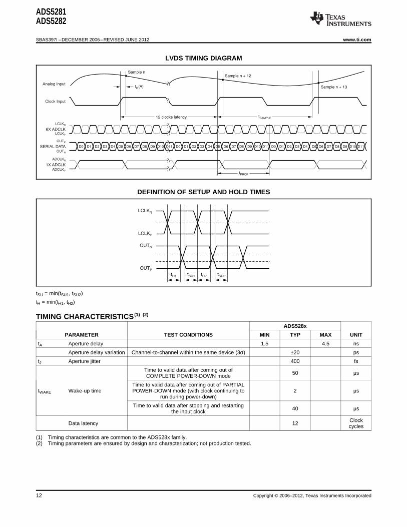

ADS5281ADS5282
wwwticom SBAS397I ndashDECEMBER 2006ndashREVISED JUNE 2012
LVDS OUTPUT TIMING CHARACTERISTICS (1) (2)
Typical values are at +25degC minimum and maximum values are measured across the specified temperature range of TMIN = ndash40degC to TMAX =+85degC sampling frequency = as specified CLOAD = 5pF (3) IOUT = 35mA RLOAD = 100Ω (4) and no internal termination unless otherwisenoted
ADS528x
40MSPS 50MSPS 65MSPS
PARAMETER TEST CONDITIONS (5) MIN TYP MAX MIN TYP MAX MIN TYP MAX UNIT
Data valid (7) to zero-crossing oftSU Data setup time(6) 067 047 027 ns
LCLKP
Zero-crossing of LCLKP to datatH Data hold time(6) 085 065 04 ns
becoming invalid(7)
Input clock (ADCLK) rising edgetPROP Clock propagation delay cross-over to output clock (ADCLKP) 10 14 166 10 125 141 97 115 14 ns
rising edge cross-over
Duty cycle of differential clockLVDS bit clock duty cycle 455 50 53 45 50 535 41 50 57
(LCLKP ndash LCLKN)
Bit clock cycle-to-cycle250 250 250 ps pp
jitter
Frame clock cycle-to-cycle150 150 150 ps pp
jitter
tRISE Data rise time data fall Rise time is from ndash100mV to +100mV009 02 04 009 02 04 009 02 04 ns
tFALL time Fall time is from +100mV to ndash100mV
tCLKRISE Output clock rise time Rise time is from ndash100mV to +100mV009 02 04 009 02 04 009 02 04 ns
tCLKFALL output clock fall time Fall time is from +100mV to ndash100mV
(1) All characteristics are at the maximum rated speed for each speed grade(2) Timing parameters are ensured by design and characterization not production tested(3) CLOAD is the effective external single-ended load capacitance between each output pin and ground(4) IOUT refers to the LVDS buffer current setting RLOAD is the differential load resistance between the LVDS output pair(5) Measurements are done with a transmission line of 100Ω characteristic impedance between the device and the load(6) Setup and hold time specifications take into account the effect of jitter on the output data and clock These specifications also assume
that data and clock paths are perfectly matched within the receiver Any mismatch in these paths within the receiver would appear asreduced timing margin
(7) Data valid refers to a logic high of +100mV and a logic low of ndash100mV
LVDS OUTPUT TIMING CHARACTERISTICS (1) (2)
Typical values are at +25degC minimum and maximum values are measured across the specified temperature range of TMIN = ndash40degC to TMAX =+85degC sampling frequency = as specified CLOAD = 5pF (3) IOUT = 35mA RLOAD = 100Ω (4) and no internal termination unless otherwisenoted
ADS528x
30MSPS 20MSPS 10MSPS
PARAMETER TEST CONDITIONS (5) MIN TYP MAX MIN TYP MAX MIN TYP MAX UNIT
Data valid (7) to zero-crossing oftSU Data setup time(6) 08 15 37 ns
LCLKP
Zero-crossing of LCLKP to datatH Data hold time(6) 12 19 39 ns
becoming invalid(7)
Input clock (ADCLK) rising edgetPROP Clock propagation delay cross-over to output clock (ADCLKP) 95 135 173 95 145 173 10 147 171 ns
rising edge cross-over
Duty cycle of differential clockLVDS bit clock duty cycle 465 50 52 48 50 51 49 50 51
(LCLKP ndash LCLKN)
Bit clock cycle-to-cycle250 250 750 ps pp
jitter
Frame clock cycle-to-cycle150 150 500 ps pp
jitter
tRISE Data rise time data fall Rise time is from ndash100mV to +100mV009 02 04 009 02 04 009 02 04 ns
tFALL time Fall time is from +100mV to ndash100mV
tCLKRISE Output clock rise time Rise time is from ndash100mV to +100mV009 02 04 009 02 04 009 02 04 ns
tCLKFALL output clock fall time Fall time is from +100mV to ndash100mV
(1) All characteristics are at the speeds other than the maximum rated speed for each speed grade(2) Timing parameters are ensured by design and characterization not production tested(3) CLOAD is the effective external single-ended load capacitance between each output pin and ground(4) IOUT refers to the LVDS buffer current setting RLOAD is the differential load resistance between the LVDS output pair(5) Measurements are done with a transmission line of 100Ω characteristic impedance between the device and the load(6) Setup and hold time specifications take into account the effect of jitter on the output data and clock These specifications also assume
that data and clock paths are perfectly matched within the receiver Any mismatch in these paths within the receiver would appear asreduced timing margin
(7) Data valid refers to a logic high of +100mV and a logic low of ndash100mV
Copyright copy 2006ndash2012 Texas Instruments Incorporated 13
t1
t2
t3
AVDD (3V to 36V)
LVDD (17V to 19V)
High-Level RESET
(14V to 36V)
High-Level CS
(14V to 36V)
Device Ready for
Serial Register Write(2)
Device Ready for
Data ConversionStart of Clock
AVDD
LVDD
RESET
CS
ADCLK
t4 t7
t5
t8
t6
ADS5281ADS5282
SBAS397I ndashDECEMBER 2006ndashREVISED JUNE 2012 wwwticom
LVDS OUTPUT TIMING CHARACTERISTICSTIMINGS WHEN USING REGISTER 0xE3 (2)
At 40 MSPSPARAMETER (1) TEST CONDITIONS
MIN TYP MAX
Data setup time Data valid (3) to zero-crossing of LCLKp 060
Data hold time Zero-crossing of LCLKP to data becoming invalid(3) 092
Input clock (ADCLK) rising edge cross-over to output clock (ADCLK) rising edgeClock propagation delay 8 12 146
crossover
(1) Only the setup time hold time and clock propagation delay parameters are affected Rest of the parameters are same as given inprevious two tables
(2) Only timing specifications for 40MSPS are affected when using register 0xE3 (as specified in the recommended operating table section)The timing specifications for other clock frequencies are same as given in previous two tables
(3) Data valid refers to logic high of +100mV and logic low of ndash100mV
RECOMMENDED POWER-UP SEQUENCING AND RESET TIMING
10μs lt t1 lt 50ms 10μs lt t2 lt 50ms ndash10ms lt t3 lt 10ms t4 gt 10ms t5 gt 100ns t6 gt 100ns t7 gt 10ms and t8 gt 100μs
(1) The AVDD and LVDD power on sequence does not matter as long as ndash10ms lt t3 lt 10ms Similar considerations apply while shuttingdown the device
(2) Write initialization registers listed in the Initialization Registers table
14 Copyright copy 2006ndash2012 Texas Instruments Incorporated
PD
Device Fully
Powers DownDevice Fully
Powers Up
tWAKE1 sm
ADS5281ADS5282
wwwticom SBAS397I ndashDECEMBER 2006ndashREVISED JUNE 2012
POWER-DOWN TIMING
Power-up time shown is based on 1μF bypass capacitors on the reference pins tWAKE is the time it takes for the device to wake upcompletely from power-down mode The ADS528x has two power-down modes complete power-down mode and partial power-down modeThe device can be configured in partial power-down mode through a register setting
tWAKE lt 50μs for complete power-down mode
tWAKE lt 2μs for partial power-down mode (provided the clock is not shut off during power-down)
Copyright copy 2006ndash2012 Texas Instruments Incorporated 15
D15 D14 D13 D12 D11 D10 D9 D8 D7 D6 D5 D4 D3 D2 D1 D0A7 A6 A5 A4 A3 A2 A1 A0
CS
SCLK
SDATA
Data latched on rising edge of SCLK
Start Sequence End Sequence
t6
t4
t2
t7
t3
t5
t1
ADS5281ADS5282
SBAS397I ndashDECEMBER 2006ndashREVISED JUNE 2012 wwwticom
SERIAL INTERFACE
The ADS528x has a set of internal registers that can be accessed through the serial interface formed by pins CS(chip select active low) SCLK (serial interface clock) and SDATA (serial interface data) When CS is low thefollowing actions occurbull Serial shift of bits into the device is enabledbull SDATA (serial data) is latched at every rising edge of SCLKbull SDATA is loaded into the register at every 24th SCLK rising edge
If the word length exceeds a multiple of 24 bits the excess bits are ignored Data can be loaded in multiples of24-bit words within a single active CS pulse The first eight bits form the register address and the remaining 16bits form the register data The interface can work with SCLK frequencies from 20MHz down to very low speeds(a few hertz) and also with a non-50 SCLK duty cycle
Register Initialization
After power-up the internal registers must be initialized to the respective default values Initialization can bedone in one of two ways1 Through a hardware reset by applying a low-going pulse on the RESET pin or2 Through a software reset using the serial interface set the RST bit high Setting this bit initializes the
internal registers to the respective default values and then self-resets the RST bit low In this case theRESET pin stays high (inactive)
After all registers have been initialized to their default values through a RESET operation the registers detailedin the Initialization Registers table must be written into This process must be done after every hardware orsoftware RESET operation in order to reconfigure the device for the best mode of operation
SERIAL INTERFACE TIMING
ADS528x
PARAMETER DESCRIPTION MIN TYP MAX UNIT
t1 SCLK period 50 ns
t2 SCLK high time 20 ns
t3 SCLK low time 20 ns
t4 Data setup time 5 ns
t5 Data hold time 5 ns
t6 CS fall to SCLK rise 8 ns
t7 Time between last SCLK rising edge to CS rising edge 8 ns
16 Copyright copy 2006ndash2012 Texas Instruments Incorporated
ADS5281ADS5282
wwwticom SBAS397I ndashDECEMBER 2006ndashREVISED JUNE 2012
SERIAL REGISTER MAP
Table 4 SUMMARY OF FUNCTIONS SUPPORTED BY SERIAL INTERFACE (1) (2) (3) (4)
ADDRESSIN HEX D15 D14 D13 D12 D11 D10 D9 D8 D7 D6 D5 D4 D3 D2 D1 D0 NAME DESCRIPTION DEFAULT
00 X RST Self-clearing software RESET Inactive
Channel-specific ADC power-X X X X X X X X PDN_CHlt81gt Inactive
down mode
Partial power-down mode (fastX PDN_PARTIAL Inactive
recovery from power-down)0F
Register mode for completeX PDN_COMPLETE Inactive
power-down (slower recovery)
Configures the PD pin for partial CompleteX PDN_PIN_CFG
power-down mode power-down
LVDS current driveX X X ILVDS_LCLKlt20gt programmability for LCLKN and 35mA drive
LCLKP pins
LVDS current driveILVDS_FRAME
11 X X X programmability for ADCLKN and 35mA drivelt20gt
ADCLKP pins
LVDS current driveX X X ILVDS_DATlt20gt programmability for OUTN and 35mA drive
OUTP pins
Enables internal termination for TerminationX EN_LVDS_TERM
LVDS buffers disabled
Programmable termination for Termination1 X X X TERM_LCLKlt20gt
LCLKN and LCLKP buffers disabled12
TERM_FRAME Programmable termination for Termination1 X X X
lt20gt ADCLKN and ADCLKP buffers disabled
Programmable termination for Termination1 X X X TERM_DATlt20gt
OUTN and OUTP buffers disabled
Channel-specific low-frequency14 X X X X X X X X LFNS_CHlt81gt Inactive
noise suppression mode enable
INP isSwaps the polarity of the analog
24 X X X X X X X X INVERT_CHlt81gt positiveinput pins electrically
input
Enables a repeating full-scaleX 0 0 EN_RAMP Inactive
ramp pattern on the outputs
Enables the mode wherein theDUALCUSTOM_
0 X 0 output toggles between two InactivePAT
defined codes
Enables the mode wherein theSINGLE_CUSTOM
0 0 X output is a constant specified Inactive25 _PAT
code
2MSBs for a single customBITS_CUSTOM1 pattern (and for the first code of
X X Inactivelt1110gt the dual custom pattern) lt11gt is
the MSB
BITS_CUSTOM2 2MSBs for the second code ofX X Inactive
lt1110gt the dual custom pattern
10 lower bits for the singleBITS_CUSTOM1 custom pattern (and for the first
26 X X X X X X X X X X Inactivelt90gt code of the dual custom pattern)
lt0gt is the LSB
BITS_CUSTOM2 10 lower bits for the second27 X X X X X X X X X X Inactive
lt90gt code of the dual custom pattern
X X X X GAIN_CH1lt30gt Programmable gain channel 1 0dB gain
X X X X GAIN_CH2lt30gt Programmable gain channel 2 0dB gain2A
X X X X GAIN_CH3lt30gt Programmable gain channel 3 0dB gain
X X X X GAIN_CH4lt30gt Programmable gain channel 4 0dB gain
X X X X GAIN_CH5lt30gt Programmable gain channel 5 0dB gain
X X X X GAIN_CH6lt30gt Programmable gain channel 6 0dB gain2B
X X X X GAIN_CH7lt30gt Programmable gain channel 7 0dB gain
X X X X GAIN_CH8lt30gt Programmable gain channel 8 0dB gain
(1) The unused bits in each register (identified as blank table cells) must be programmed as 0(2) X = Register bit referenced by the corresponding name and description (default is 0)(3) Bits marked as 0 should be forced to 0 and bits marked as 1 should be forced to 1 when the particular register is programmed(4) Multiple functions in a register should be programmed in a single write operation
Copyright copy 2006ndash2012 Texas Instruments Incorporated 17
ADS5281ADS5282
SBAS397I ndashDECEMBER 2006ndashREVISED JUNE 2012 wwwticom
Table 4 SUMMARY OF FUNCTIONS SUPPORTED BY SERIAL INTERFACE(1) (2) (3) (4) (continued)ADDRESS
IN HEX D15 D14 D13 D12 D11 D10 D9 D8 D7 D6 D5 D4 D3 D2 D1 D0 NAME DESCRIPTION DEFAULT
Single-1 X DIFF_CLK Differential clock mode
ended clock
Enables the duty-cycle correction1 X EN_DCC Disabled
circuit
External42Drives the external reference reference
1 X EXT_REF_VCMmode through the VCM pin drives REFT
and REFB
Controls the phase of LCLK1 X X PHASE_DDRlt10gt 90 degrees
output relative to data
0 X PAT_DESKEW Enables deskew pattern mode Inactive45
X 0 PAT_SYNC Enables sync pattern mode Inactive
Binary twos complement format Straight1 1 X BTC_MODE
for ADC output offset binary
Serialized ADC output comes LSB-first1 1 X MSB_FIRST
out MSB-first output
Enables SDR output modeDDR output46 1 1 X EN_SDR (LCLK becomes a 12x input
modeclock)
Controls whether the LCLK rising Rising edgeor falling edge comes in the of LCLK in
1 X 1 1 FALL_SDRmiddle of the data window when middle ofoperating in SDR output mode data window
SUMMARY OF FEATURES
POWER IMPACT (relative to default)FEATURES DEFAULT SELECTION AT fS = 65MSPS
ANALOG FEATURES
Internal or external reference Internal reference mode uses approximately 23mW moreNA Pin(driven on the REFT and REFB pins) power on AVDD
External reference driven on the Off Register 42 Approximately 9mW less power on AVDDVCM pin
Duty cycle correction circuit Off Register 42 Approximately 7mW more power on AVDD
With zero input to the ADC low-frequency noise suppressionLow-frequency noise suppression Off Register 14 causes digital switching at fS2 thereby increasing LVDD
power by approximately 7mWchannel
Differential clock mode uses approximately 7mW more powerSingle-ended or differential clock Single-ended Register 42 on AVDD
Refer to the Power-Down Modes section in the ElectricalPower-down mode Off Pin and register 0F Characteristics table
DIGITAL FEATURES
Programmable digital gain (0dB to Registers 2A and0dB No difference12dB) 2B
Straight offset or BTC output Straight offset Register 46 No difference
Swap polarity of analog input pins Off Register 24 No difference
LVDS OUTPUT PHYSICAL LAYER
LVDS internal termination Off Register 12 Approximately 7mW more power on AVDD
LVDS current programmability 35mA Register 11 As per LVDS clock and data buffer current setting
LVDS OUTPUT TIMING
LSB- or MSB-first output LSB-first Register 46 No difference
SDR mode uses approximately 2mW more power on LVDDDDR or SDR output DDR Register 46 (at fS = 30MSPS)
Refer toLCLK phase relative to data output Register 42 No differenceFigure 1
18 Copyright copy 2006ndash2012 Texas Instruments Incorporated
ADS5281ADS5282
wwwticom SBAS397I ndashDECEMBER 2006ndashREVISED JUNE 2012
DESCRIPTION OF SERIAL REGISTERS
SOFTWARE RESET
ADDRESSIN HEX D15 D14 D13 D12 D11 D10 D9 D8 D7 D6 D5 D4 D3 D2 D1 D0 NAME
00 X RST
Software reset is applied when the RST bit is set to 1 setting this bit resets all internal registers and self-clearsto 0
POWER-DOWN MODES
ADDRESSIN HEX D15 D14 D13 D12 D11 D10 D9 D8 D7 D6 D5 D4 D3 D2 D1 D0 NAME
X X X X X X X X PDN_CHlt81gt
X PDN_PARTIAL0F
0 X PDN_COMPLETE
X 0 PDN_PIN_CFG
Each of the eight channels can be individually powered down PDN_CHltNgt controls the power-down mode forthe ADC channel ltNgt
In addition to channel-specific power-down the ADS528x also has two global power-down modesmdashpartialpower-down mode and complete power-down mode Partial power-down mode partially powers down the chiprecovery from this mode is much quicker provided that the clock has been running for at least 50μs beforeexiting this mode Complete power-down mode on the other hand completely powers down the chip andinvolves a much longer recovery time
In addition to programming the device for either of these two power-down modes (through either thePDN_PARTIAL or PDN_COMPLETE bits respectively) the PD pin itself can be configured as either a partialpower-down pin or a complete power-down pin control For example if PDN_PIN_CFG = 0 (default) when thePD pin is high the device enters complete power-down mode However if PDN_PIN_CFG = 1 when the PD pinis high the device enters partial power-down mode
LVDS DRIVE PROGRAMMABILITY
ADDRESSIN HEX D15 D14 D13 D12 D11 D10 D9 D8 D7 D6 D5 D4 D3 D2 D1 D0 NAME
X X X ILVDS_LCLKlt20gt
11 X X X ILVDS_FRAMElt20gt
X X X ILVDS_DATlt20gt
The LVDS drive strength of the bit clock (LCLKP or LCLKN) and the frame clock (ADCLKP or ADCLKN) can beindividually programmed The LVDS drive strengths of all the data outputs OUTP and OUTN can also beprogrammed to the same value
Copyright copy 2006ndash2012 Texas Instruments Incorporated 19
ADS5281ADS5282
SBAS397I ndashDECEMBER 2006ndashREVISED JUNE 2012 wwwticom
All three drive strengths (bit clock frame clock and data) are programmed using sets of three bits Table 5shows an example of how the drive strength of the bit clock is programmed (the method is similar for the frameclock and data drive strengths)
Table 5 Bit Clock Drive Strength (1)
ILVDS_LCLKlt2gt ILVDS_LCLKlt1gt ILVDS_LCLKlt0gt LVDS DRIVE STRENGTH FOR LCLKP AND LCLKN
0 0 0 35mA (default)
0 0 1 25mA
0 1 0 15mA
0 1 1 05mA
1 0 0 75mA
1 0 1 65mA
1 1 0 55mA
1 1 1 45mA
(1) Current settings lower than 15mA are not recommended
LVDS INTERNAL TERMINATION PROGRAMMABILITY
ADDRESSIN HEX D15 D14 D13 D12 D11 D10 D9 D8 D7 D6 D5 D4 D3 D2 D1 D0 NAME
X EN_LVDS_TERM
1 X X X TERM_LCLKlt20gt12
1 X X X TERM_FRAMElt20gt
1 X X X TERM_DATlt20gt
The LVDS buffers have high-impedance current sources driving the outputs When driving traces whosecharacteristic impedance is not perfectly matched with the termination impedance on the receiver side there maybe reflections back to the LVDS output pins of the ADS528x that cause degraded signal integrity By enabling aninternal termination (between the positive and negative outputs) for the LVDS buffers the signal integrity can besignificantly improved in such scenarios To set the internal termination mode the EN_LVDS_TERM bit shouldbe set to 1 Once this bit is set the internal termination values for the bit clock frame clock and data bufferscan be independently programmed using sets of three bits Table 6 shows an example of how the internaltermination of the LVDS buffer driving the bit clock is programmed (the method is similar for the frame clock anddata buffers) These termination values are only typical values and can vary by up to plusmn20 across temperatureand from device to device
Table 6 Bit Clock Internal Termination
INTERNAL TERMINATION BETWEENTERM_LCLKlt2gt TERM_LCLKlt1gt TERM_LCLKlt0gt LCLKP AND LCLKN IN Ω
0 0 0 None
0 0 1 260
0 1 0 150
0 1 1 94
1 0 0 125
1 0 1 80
1 1 0 66
1 1 1 55
20 Copyright copy 2006ndash2012 Texas Instruments Incorporated
ADS5281ADS5282
wwwticom SBAS397I ndashDECEMBER 2006ndashREVISED JUNE 2012
LOW-FREQUENCY NOISE SUPPRESSION MODE
ADDRESSIN HEX D15 D14 D13 D12 D11 D10 D9 D8 D7 D6 D5 D4 D3 D2 D1 D0 NAME
14 X X X X X X X X LFNS_CHlt81gt
The low-frequency noise suppression mode is specifically useful in applications where good noise performance isdesired in the frequency band of 0MHz to 1MHz (around dc) Setting this mode shifts the low-frequency noise ofthe ADS528x to approximately fS2 thereby moving the noise floor around dc to a much lower valueLFNS_CHlt81gt enables this mode individually for each channel
ANALOG INPUT INVERT
ADDRESSIN HEX D15 D14 D13 D12 D11 D10 D9 D8 D7 D6 D5 D4 D3 D2 D1 D0 NAME
24 X X X X X X X X INVERT_CHlt81gt
Normally the INP pin represents the positive analog input pin and INN represents the complementary negativeinput Setting the bits marked INVERT_CHlt81gt (individual control for each channel) causes the inputs to beswapped INN now represents the positive input and INP the negative input
LVDS TEST PATTERNS
ADDRESSIN HEX D15 D14 D13 D12 D11 D10 D9 D8 D7 D6 D5 D4 D3 D2 D1 D0 NAME
X 0 0 EN_RAMP
0 X 0 DUALCUSTOM_PAT
25 0 0 X SINGLE_CUSTOM_PAT
X X BITS_CUSTOM1lt1110gt
X X BITS_CUSTOM2lt1110gt
26 X X X X X X X X X X BITS_CUSTOM1lt90gt
27 X X X X X X X X X X BITS_CUSTOM2lt90gt
0 X PAT_DESKEW45
X 0 PAT_SYNC
The ADS528x can output a variety of test patterns on the LVDS outputs These test patterns replace the normalADC data output Setting EN_RAMP to 1 causes all the channels to output a repeating full-scale ramp patternThe ramp increments from zero code to full-scale code in steps of 1LSB every clock cycle After hitting the full-scale code it returns back to zero code and ramps again
The device can also be programmed to output a constant code by setting SINGLE_CUSTOM_PAT to 1 andprogramming the desired code in BITS_CUSTOM1lt110gt In this mode BITS_CUSTOM1lt110gt take the placeof the 12-bit ADC data at the output and are controlled by LSB-first and MSB-first modes in the same way asnormal ADC data are
The device may also be made to toggle between two consecutive codes by programming DUAL_CUSTOM_PATto 1 The two codes are represented by the contents of BITS_CUSTOM1lt110gt and BITS_CUSTOM2lt110gt
In addition to custom patterns the device may also be made to output two preset patterns1 Deskew patten Set using PAT_DESKEW this mode replaces the 12-bit ADC output Dlt110gt with the
010101010101 word2 Sync pattern Set using PAT_SYNC the normal ADC word is replaced by a fixed 111111000000 word
Note that only one of the above patterns should be active at any given instant
Copyright copy 2006ndash2012 Texas Instruments Incorporated 21
ADS5281ADS5282
SBAS397I ndashDECEMBER 2006ndashREVISED JUNE 2012 wwwticom
PROGRAMMABLE GAIN
ADDRESSIN HEX D15 D14 D13 D12 D11 D10 D9 D8 D7 D6 D5 D4 D3 D2 D1 D0 NAME
X X X X GAIN_CH1lt30gt
X X X X GAIN_CH2lt30gt2A
X X X X GAIN_CH3lt30gt
X X X X GAIN_CH4lt30gt
X X X X GAIN_CH5lt30gt
X X X X GAIN_CH6lt30gt2B
X X X X GAIN_CH7lt30gt
X X X X GAIN_CH8lt30gt
In applications where the full-scale swing of the analog input signal is much less than the 2VPP range supportedby the ADS528x a programmable gain can be set to achieve the full-scale output code even with a lower analoginput swing The programmable gain not only fills the output code range of the ADC but also enhances the SNRof the device by utilizing quantization information from some extra internal bits The programmable gain for eachchannel can be individually set using a set of four bits indicated as GAIN_CHNlt30gt for Channel N The gainsetting is coded in binary from 0dB to 12dB as shown in Table 7
Table 7 Gain Setting for Channel 1
GAIN_CH1lt3gt GAIN_CH1lt2gt GAIN_CH1lt1gt GAIN_CH1lt0gt CHANNEL 1 GAIN SETTING
0 0 0 0 0dB
0 0 0 1 1dB
0 0 1 0 2dB
0 0 1 1 3dB
0 1 0 0 4dB
0 1 0 1 5dB
0 1 1 0 6dB
0 1 1 1 7dB
1 0 0 0 8dB
1 0 0 1 9dB
1 0 1 0 10dB
1 0 1 1 11dB
1 1 0 0 12dB
1 1 0 1 Do not use
1 1 1 0 Do not use
1 1 1 1 Do not use
22 Copyright copy 2006ndash2012 Texas Instruments Incorporated
VREF = 15V -B
VCM
15V
VREF = 15V +T
VCM
15V
ADS5281ADS5282
wwwticom SBAS397I ndashDECEMBER 2006ndashREVISED JUNE 2012
CLOCK REFERENCE AND DATA OUTPUT MODES
ADDRESSIN HEX D15 D14 D13 D12 D11 D10 D9 D8 D7 D6 D5 D4 D3 D2 D1 D0 NAME
1 X DIFF_CLK
1 X EN_DCC42
1 X EXT_REF_VCM
1 X X PHASE_DDRlt10gt
1 1 X BTC_MODE
1 1 X MSB_FIRST46
1 1 X EN_SDR
1 X 1 1 FALL_SDR
INPUT CLOCK
The ADS528x is configured by default to operate with a single-ended input clockmdashCLKP is driven by a CMOSclock and CLKN is tied to 0 However by programming DIFF_CLK to 1 the device can be made to work with adifferential input clock on CLKP and CLKN Operating with a low-jitter differential clock usually gives better SNRperformance especially at input frequencies greater than 30MHz
In cases where the duty cycle of the input clock falls outside the 45 to 55 range it is recommended to enablean internal duty cycle correction circuit This enabling is done by setting the EN_DCC bit to 1
EXTERNAL REFERENCE
The ADS528x can be made to operate in external reference mode by pulling the INTEXT pin to 0 In this modethe REFT and REFB pins should be driven with voltage levels of 25V and 05V respectively and must haveenough drive strength to drive the switched capacitance loading of the reference voltages by each ADC Theadvantage of using the external reference mode is that multiple ADS528x units can be made to operate with thesame external reference thereby improving parameters such as gain matching across devices However inapplications that do not have an available high drive differential external reference the ADS528x can still bedriven with a single external reference voltage on the VCM pin When EXT_REF_VCM is set as 1 (and theINTEXT pin is set to 0) the VCM pin is configured as an input pin and the voltages on REFT and REFB aregenerated as shown in Equation 1 and Equation 2
(1)
(2)
Copyright copy 2006ndash2012 Texas Instruments Incorporated 23
PHASE_DDRlt10gt = 00
PHASE_DDRlt10gt = 01
PHASE_DDRlt10gt = 10
PHASE_DDRlt10gt = 11
ADCLKP
LCLKP
OUTP
ADCLKP
LCLKP
OUTP
ADCLKP
LCLKP
OUTP
ADCLKP
LCLKP
OUTP
ADCLKP
LCLKP
OUTP
ADS5281ADS5282
SBAS397I ndashDECEMBER 2006ndashREVISED JUNE 2012 wwwticom
BIT CLOCK PROGRAMMABILITY
The output interface of the ADS528x is normally a DDR interface with the LCLK rising edge and falling edgetransitions in the middle of alternate data windows This default phase is shown in Figure 1
Figure 1 Default Phase of LCLK
The phase of LCLK can be programmed relative to the output frame clock and data using bitsPHASE_DDRlt10gt The LCLK phase modes are shown in Figure 2
Figure 2 Phase Programmability Modes for LCLK
24 Copyright copy 2006ndash2012 Texas Instruments Incorporated
EN_SDR = 1 FALL_SDR = 0
EN_SDR = 1 FALL_SDR = 1
ADCLKP
LCLKP
OUTP
ADCLKP
LCLKP
OUTP
ADS5281ADS5282
wwwticom SBAS397I ndashDECEMBER 2006ndashREVISED JUNE 2012
In addition to programming the phase of LCLK in the DDR mode the device can also be made to operate in SDRmode by setting the EN_SDR bit to 1 In this mode the bit clock (LCLK) is output at 12x times the input clock ortwice the rate as in DDR mode Depending on the state of FALL_SDR LCLK may be output in either of the twomanners shown in Figure 3 As can be seen in Figure 3 only the LCLK rising (or falling) edge is used to capturethe output data in SDR mode
Figure 3 SDR Interface Modes
The SDR mode does not work well beyond 40MSPS because the LCLK frequency becomes very high
DATA OUTPUT FORMAT MODES
The ADC output by default is in straight offset binary mode Programming the BTC_MODE bit to 1 inverts theMSB and the output becomes binary twos complement mode
Also by default the first bit of the frame (following the rising edge of ADCLKP) is the LSB of the ADC outputProgramming the MSB_FIRST mode inverts the bit order in the word and the MSB is output as the first bitfollowing the ADCLKP rising edge
Copyright copy 2006ndash2012 Texas Instruments Incorporated 25
0
-
-
-
-
-
-
-
-
-
20
40
60
80
100
120
140
160
180
Input Frequency (MHz)
0 25
Am
plit
ude (
dB
)
2015105
SFDR = 884dBc
SNR = 709dBFS
SINAD = 708dBFS
THD = 875dBc
0
-
-
-
-
-
-
-
-
-
20
40
60
80
100
120
140
160
180
Input Frequency (MHz)
0 25
Am
plit
ude (
dB
)
2015105
SFDR = 856dBc
SNR = 705dBFS
SINAD = 704dBFS
THD = 839dBc
0
-
-
-
-
-
-
-
-
-
20
40
60
80
100
120
140
160
180
Input Frequency (MHz)
0 2 20
Am
plit
ude (
dB
)
1816141210864
SFDR = 853dBc
SNR = 708dBFS
SINAD = 707dBFS
THD = 893dBc
0
-
-
-
-
-
-
-
-
-
20
40
60
80
100
120
140
160
180
Input Frequency (MHz)
0 2 20
Am
plit
ude (
dB
)
1816141210864
SFDR = 828dBc
SNR = 702dBFS
SINAD = 70dBFS
THD = 823dBc
ADS5281ADS5282
SBAS397I ndashDECEMBER 2006ndashREVISED JUNE 2012 wwwticom
TYPICAL CHARACTERISTICSAt TA = +25degC AVDD = +33V LVDD = 18V clock frequency = 65MSPS differential clock mode 1VPP clock amplitude 50
clock duty cycle input frequency = 10MHz ndash1dBFS differential analog input 0dB digital gain setting 15V analog inputcommon-mode low-frequency noise suppression = off internal reference mode ISET resistor = 562kΩ and LVDS buffer
current setting = 35mA unless otherwise noted
SPECTRAL PERFORMANCE SPECTRAL PERFORMANCE(fS = 40MHz fIN = 10MHz) (fS = 40MHz fIN = 25MHz)
Figure 4 Figure 5
SPECTRAL PERFORMANCE SPECTRAL PERFORMANCE(fS = 50MHz fIN = 10MHz) (fS = 50MHz fIN = 25MHz)
Figure 6 Figure 7
26 Copyright copy 2006ndash2012 Texas Instruments Incorporated
0
-20
-40
-60
-80
-100
-120
-140
-180
Input Frequency (MHz)
0 33
Am
plit
ude (
dB
)
2015105
-160
SFDR = 862dBc
SNR = 705dBFS
SNR (0MHz to 1MHz) = 861dBFS
SINAD = 704dBFS
THD = 854dBc
25 30
92
87
82
77
72
67
Input Frequency (MHz)
5 30
Dynam
ic P
erf
orm
ance (
SN
R S
FD
R)
201510 25
SNR (dBFS)
SFDR (dBc)
f = 40MHzS
0
-
-
-
-
-
-
-
-
-
20
40
60
80
100
120
140
160
180
Input Frequency (MHz)
0 33
Am
plit
ude (
dB
)
2015105 25 30
SFDR = 909dBc
SNR = 708dBFS
SINAD = 707dBFS
THD = 904dBc
0
-20
-40
-60
-80
-100
-120
-140
-180
Input Frequency (MHz)
0 33
Am
plit
ude (
dB
)
2015105
-160
SFDR = 874dBc
SNR = 704dBFS
SNR (0MHz to 1MHz) = 819dBFS
SINAD = 703dBFS
THD = 864dBc
25 30
ADS5281ADS5282
wwwticom SBAS397I ndashDECEMBER 2006ndashREVISED JUNE 2012
TYPICAL CHARACTERISTICS (continued)At TA = +25degC AVDD = +33V LVDD = 18V clock frequency = 65MSPS differential clock mode 1VPP clock amplitude 50clock duty cycle input frequency = 10MHz ndash1dBFS differential analog input 0dB digital gain setting 15V analog inputcommon-mode low-frequency noise suppression = off internal reference mode ISET resistor = 562kΩ and LVDS buffercurrent setting = 35mA unless otherwise noted
SPECTRAL PERFORMANCE SPECTRAL PERFORMANCE(fS = 65MHz fIN = 10MHz) (fS = 65MHz fIN = 25MHz)
Figure 8 Figure 9
SPECTRAL PERFORMANCE LOW-FREQUENCY NOISESUPPRESSION MODE ENABLED
(fS = 65MHz fIN = 25MHz) DYNAMIC PERFORMANCE vs INPUT FREQUENCY
Figure 10 Figure 11
Copyright copy 2006ndash2012 Texas Instruments Incorporated 27
95
85
75
65
55
45
35
25
Input Amplitude (dBFS)
Dyn
am
ic P
erf
orm
an
ce
(S
NR
S
FD
R)
SNR (dBFS)
SFDR (dBc)
f = 65MHz
f = 10MHzS
IN
-60 0-50 -40 -30 -20 -10
94
89
84
79
74
69
Clock Amplitude (V Differential)PP
06 23
Dynam
ic P
erf
orm
ance (
SN
R S
FD
R)
1611
SNR (dBFS)
SFDR (dBc)
f = 65MHz
f = 10MHzS
IN
21
95
90
85
80
75
70
65
60
Digital Gain (dB)
0 12
Dyn
am
ic P
erf
orm
an
ce
(S
NR
S
FD
R)
642 8
SNR (dBFS)
SFDR (dBc)
f = 65MHz
f = 10MHzS
IN
10
95
90
85
80
75
70
65
60
AVDD (V)
30 36
Dynam
ic P
erf
orm
ance (
SN
R S
FD
R)
333231 34
SNR (dBFS)
SFDR (dBc)
f = 65MHz
f = 10MHzS
IN
35
92
87
82
77
72
67
Input Frequency (MHz)
5 30
Dynam
ic P
erf
orm
ance (
SN
R S
FD
R)
201510 25
SNR (dBFS)
SFDR (dBc)
f = 50MHzS
97
92
87
82
77
72
67
Input Frequency (MHz)
5 30
Dynam
ic P
erf
orm
ance (
SN
R S
FD
R)
201510 25
SNR (dBFS)
SFDR (dBc)
f = 65MHzS
ADS5281ADS5282
SBAS397I ndashDECEMBER 2006ndashREVISED JUNE 2012 wwwticom
TYPICAL CHARACTERISTICS (continued)At TA = +25degC AVDD = +33V LVDD = 18V clock frequency = 65MSPS differential clock mode 1VPP clock amplitude 50clock duty cycle input frequency = 10MHz ndash1dBFS differential analog input 0dB digital gain setting 15V analog inputcommon-mode low-frequency noise suppression = off internal reference mode ISET resistor = 562kΩ and LVDS buffercurrent setting = 35mA unless otherwise noted
DYNAMIC PERFORMANCE vs INPUT FREQUENCY DYNAMIC PERFORMANCE vs INPUT FREQUENCY
Figure 12 Figure 13
DYNAMIC PERFORMANCE vs DIGITAL GAIN DYNAMIC PERFORMANCE vs AVDD
Figure 14 Figure 15
DYNAMIC PERFORMANCE vs INPUT AMPLITUDE DYNAMIC PERFORMANCE vs CLOCK AMPLITUDE
Figure 16 Figure 17
28 Copyright copy 2006ndash2012 Texas Instruments Incorporated
94
89
84
79
74
69
External Reference Common-Mode Voltage (REF + REF )2 (V)T B
135 165
Dynam
ic P
erf
orm
ance (
SN
R S
FD
R)
150145140
SNR (dBFS)
SFDR (dBc)
f = 65MHz
f = 10MHzS
IN
155 160
External reference differential voltage maintained at 2V
94
89
84
79
74
69
Voltage on V (V)CM
135 165
Dynam
ic P
erf
orm
ance (
SN
R S
FD
R)
150145140
SNR (dBFS)
SFDR (dBc)
f = 65MHz
f = 10MHzS
IN
155 160
94
89
84
79
74
69
Analog Input Common-Mode Voltage (V)
130 170
Dynam
ic P
erf
orm
ance (
SN
R S
FD
R)
140135
SNR (dBFS)
SFDR (dBc)
f = 65MHz
f = 10MHzS
IN
145 165160155150
94
89
84
79
74
69
External Reference Differential Voltage REF REF (V)-T B
16 24
Dynam
ic P
erf
orm
ance (
SN
R S
FD
R)
191817
SNR (dBFS)
SFDR (dBc)
f = 65MHz
f = 10MHzS
IN
20 232221
External reference common-mode voltage
maintained at 15V
ADS5281ADS5282
wwwticom SBAS397I ndashDECEMBER 2006ndashREVISED JUNE 2012
TYPICAL CHARACTERISTICS (continued)At TA = +25degC AVDD = +33V LVDD = 18V clock frequency = 65MSPS differential clock mode 1VPP clock amplitude 50clock duty cycle input frequency = 10MHz ndash1dBFS differential analog input 0dB digital gain setting 15V analog inputcommon-mode low-frequency noise suppression = off internal reference mode ISET resistor = 562kΩ and LVDS buffercurrent setting = 35mA unless otherwise noted
DYNAMIC PERFORMANCE vs ANALOG INPUT COMMON- DYNAMIC PERFORMANCE vs EXTERNAL REFERENCEMODE VOLTAGE DIFFERENTIAL VOLTAGE
Figure 18 Figure 19
DYNAMIC PERFORMANCE vs EXTERNAL REFERENCE DYNAMIC PERFORMANCE vs EXTERNAL REFERENCECOMMON-MODE VOLTAGE FORCED THROUGH VCM
Figure 20 Figure 21
Copyright copy 2006ndash2012 Texas Instruments Incorporated 29
05
04
03
02
01
0
-01
-02
-05
Code (LSB)
0 4096
INL
(L
SB
)
30722048 25601536 35841024512
-04
-03
f = 50MSPS
f = 5MHzS
IN
035
025
015
005
-005
-015
-035
Code (LSB)
0 4096
DN
L (
LS
B)
30722048 25601536 35841024512
-025
f = 50MSPS
f = 5MHzS
IN
60
50
40
30
20
10
0
Code Bin (LSB)
2049
Occurr
ence (
)
20532051 2054
f = 65MSPSS
2050 2052
0 0037 028
5192
4743
10
-10
-30
-50
-70
-90
-110
-130
-150
Input Frequency (MHz)
0 2 20
Am
plit
ude (
dB
)
1816141210864
f = 65MHz
f = 10MHz ( 7dBFS)
f = 161MHz ( 7dBFS)
IMD = 97dBFS
-
-
-
S
1
2
95
90
85
80
75
70
65
60
Clock Duty Cycle ()
35 65
Dynam
ic P
erf
orm
ance (
SN
R S
FD
R)
504540 55
SNR (dBFS)
SFDR (dBc)
f = 65MHz
f = 10MHzS
IN
60
95
85
80
75
70
60
Clock Duty Cycle ()
20 80
Dynam
ic P
erf
orm
ance (
SN
R S
FD
R)
504030 60
SNR (dBFS)
SFDR (dBc)
f = 65MHz
f = 10MHzS
IN
90
70
65
ADS5281ADS5282
SBAS397I ndashDECEMBER 2006ndashREVISED JUNE 2012 wwwticom
TYPICAL CHARACTERISTICS (continued)At TA = +25degC AVDD = +33V LVDD = 18V clock frequency = 65MSPS differential clock mode 1VPP clock amplitude 50clock duty cycle input frequency = 10MHz ndash1dBFS differential analog input 0dB digital gain setting 15V analog inputcommon-mode low-frequency noise suppression = off internal reference mode ISET resistor = 562kΩ and LVDS buffercurrent setting = 35mA unless otherwise noted
DYNAMIC PERFORMANCE vs CLOCK DUTY CYCLE DCC DYNAMIC PERFORMANCE vs CLOCK DUTY CYCLE DCCDISABLED ENABLED
Figure 22 Figure 23
HISTOGRAM OF OUTPUT CODE FOR ZERO INPUT INTERMODULATION DISTORTION
Figure 24 Figure 25
INTEGRAL NONLINEARITY DIFFERENTIAL NONLINEARITY
Figure 26 Figure 27
30 Copyright copy 2006ndash2012 Texas Instruments Incorporated
064
062
060
058
056
054
052
Sta
ndard
Devia
tion (
LS
B)
0 1 2 3 4 5 6
Overload Signal Amplitude (dBFS)
f = 65MSPS
f = 5MHzS
IN
Standard Deviation of
2nd Point After Overload
Standard Deviation of
1st Point After Overload
tS
16384 t (Group 1)S
Set 1 Point 1 (of 16) Set 1 Point 2 (of 16)
First point after overload (Set 1)
First point after overload (Set 2)
Second point after overload (Set 2)
Second point after overload (Set 1)
Overload
Amplitude
NOTES
Input sine wave phase is repetitive over 16384 clock cycles
16 such repetitive groups (of 16384 clock cycles) are capturedndasha total of 262144 points
Standard deviation of every set of are analyzed over the 16 groups
Worst case of all such standard deviations are plotted in the graphs
first and second points after overload
+FS
-FS
070
068
066
064
062
060
058
056
054
052
050
Sta
nd
ard
De
via
tio
n (
in L
SB
)
0 1 2 3 4 5 6
Overload Signal Amplitude (dBFS)
f = 50MSPS
f = 5MHzS
IN Standard Deviation of
2nd Point After Overload
Standard Deviation of
1st Point After Overload
170
130
110
90
70
30
Clock Frequency (MSPS)
5 75
I I
(mA
)A
VD
DLV
DD
352515 45
ILVDD
IAVDD
Zero Input on All Channels
Internal Reference Mode150
55
50
65
075
055
035
015
-005
-025
-065
Code (LSB)
0 4096
INL
(LS
B)
30722048 25601536 35841024512
-045
f = 65MSPS
f = 5MHzS
IN
035
025
015
005
-005
-015
-035
Code (LSB)
0 4096
DN
L (
LS
B)
30722048 25601536 35841024512
-025
f = 65MSPS f = 5MHzS IN
ADS5281ADS5282
wwwticom SBAS397I ndashDECEMBER 2006ndashREVISED JUNE 2012
TYPICAL CHARACTERISTICS (continued)At TA = +25degC AVDD = +33V LVDD = 18V clock frequency = 65MSPS differential clock mode 1VPP clock amplitude 50clock duty cycle input frequency = 10MHz ndash1dBFS differential analog input 0dB digital gain setting 15V analog inputcommon-mode low-frequency noise suppression = off internal reference mode ISET resistor = 562kΩ and LVDS buffercurrent setting = 35mA unless otherwise noted
INTEGRAL NONLINEARITY DIFFERENTIAL NONLINEARITY
Figure 28 Figure 29
AVDD AND LVDD POWER-SUPPLY CURRENTSvs CLOCK FREQUENCY OVERLOAD RECOVERY AT 50MSPS
Figure 30 Figure 31
OVERLOAD RECOVERY AT 65MSPS
Figure 32 Figure 33 Overload Recovery
Copyright copy 2006ndash2012 Texas Instruments Incorporated 31
ADS5281ADS5282
SBAS397I ndashDECEMBER 2006ndashREVISED JUNE 2012 wwwticom
APPLICATION INFORMATION
The ADC output goes to a serializer that operatesTHEORY OF OPERATION from a 12x clock generated by the PLL The 12 databits from each channel are serialized and sent LSBThe ADS528x devices are a family of 8-channelfirst In addition to serializing the data the serializerhigh-speed CMOS ADCs The 12 bits given out byalso generates a 1x clock and a 6x clock Theseeach channel are serialized and sent out on a singleclocks are generated in the same way the serializedpair of pins in LVDS format All eight channels of thedata are generated so these clocks maintain perfectADS528x operate from a single clock (ADCLK) Thesynchronization with the data The data and clocksampling clocks for each of the eight channels areoutputs of the serializer are buffered externally usinggenerated from the input clock using a carefullyLVDS buffers Using LVDS buffers to transmit datamatched clock buffer tree The 12x clock required forexternally has multiple advantages such as athe serializer is generated internally from ADCLKreduced number of output pins (saving routing spaceusing a phase-locked loop (PLL) A 6x and a 1x clockon the board) reduced power consumption andare also output in LVDS format along with the datareduced effects of digital noise coupling to the analogto enable easy data capture The ADS528x operatescircuit inside the ADS528xfrom internally-generated reference voltages that are
trimmed to improve to a high level of accuracy The ADS528x operates from two sets of supplies andTrimmed references improve the gain matching grounds The analog supply and ground set isacross devices and provide the option to operate the identified as AVDD and AVSS while the digital set isdevices without having to externally drive and route identified by LVDD and LVSSreference lines The nominal values of REFT andREFB are 25V and 05V respectively The ANALOG INPUTreferences are internally scaled down differentially bya factor of 2 This scaling results in a differential input The analog input consists of a switched-capacitorof ndash1V to correspond to the zero code of the ADC based differential sample-and-hold architecture Thisand a differential input of +1V to correspond to the differential topology results in very good acfull-scale code (4095 LSB) VCM (the common-mode performance even for high input frequencies at highvoltage of REFT and REFB) is also made available sampling rates The INN and INP pins must beexternally through a pin and is nominally 15V externally biased around a common-mode voltage of
15V available on VCM For a full-scale differentialThe ADC employs a pipelined converter architectureinput each input pin (INN and INP) must swingthat consists of a combination of multi-bit and single-symmetrically between VCM + 05V and VCM ndash 05Vbit internal stages Each stage feeds its data into theresulting in a 2VPP differential input swing Thedigital error correction logic ensuring excellentmaximum input peak-to-peak differential swing isdifferential linearity and no missing codes at the 12-determined to be the difference between the internalbit levelreference voltages REFT (25V nominal) and REFB(05V nominal) Figure 34 illustrates the model of theinput driving circuit
32 Copyright copy 2006ndash2012 Texas Instruments Incorporated
CM Buffer
Internal
Voltage
Reference
Input
Circuitry
INP
INN
VCM
12kW
12kW
ADS528x
(2mA) facute S
50MSPS
5nH to 9nH (TQFP-80)
2nH to 3nH (QFN-64)
15pF
to 24pF
IN OUT
INP
15pF to
25pF
1W
1000W
to 1440W
5W
to 10W
1000W
to 1440W
5nH to 9nH (TQFP-80)
2nH to 3nH (QFN-64)
INN
15pF to
25pF
1W
15W
to 25W
15W
to 30W
02pF
to 03pF
IN OUT
15pF
to 24pF
IN OUT
5W
to 10W
15W
to 25W
15W
to 30W
IN OUT
IN
OUT
16 to 32W W
IN OUT
IN OUT
OUTP
OUTN
Switches that are ON
in SAMPLE phase
Switches that are ON
in HOLD phase
ADS5281ADS5282
wwwticom SBAS397I ndashDECEMBER 2006ndashREVISED JUNE 2012
Figure 34 Analog Input Circuit Model
during ac-coupling by increasing VCM by roughlyInput Common-Mode Current 75mV When operating above 50MSPS it is
recommended that additional parallel resistors beThe input stage of all eight ADCs together sinks aadded externally to restore the input common-modecommon-mode current on the order of 2mA atto at least 14V if the inputs are to be ac-coupled50MSPS Equation 3 describes the dependency of
the common-mode current and the samplingfrequency
(3)
If the driving stage is dc-coupled to the inputs thenEquation 3 can be used to determine its common-mode drive capability and impedance The inputs canalso be ac-coupled to the INN and INP pins In thatcase the input common-mode is set by two internal12kΩ resistors connecting the input pins to VCM Thisarchitecture is shown in Figure 35
When the inputs are ac-coupled there is a drop inthe voltages at INP and INN relative to VCM This can Dashed area denotes one of eight channelsbe computed from Equation 3 At 50MSPS for
Figure 35 Common-Mode Biasing of Input Pinsexample the drop at each of the 16 input pins is150mV which is not optimal for ADC operationInitialization Registers 1 and 5 described in theInitialization Registers table can be used to partiallyreduce the effect of this input common-mode drop
Copyright copy 2006ndash2012 Texas Instruments Incorporated 33
01 Fm 50W
50W
200W
200W
INP
VCM
INN
01 Fm
12 21
47W
47W
01 Fm
01 Fm
25W
25W
11
INP
VCM
INN
ADS5281ADS5282
SBAS397I ndashDECEMBER 2006ndashREVISED JUNE 2012 wwwticom
Driving Circuit At high input frequencies the mismatch in thetransformer parasitic capacitance (between theFor optimum performance the analog inputs must bewindings) results in degraded even-order harmonicdriven differentially This approach improves theperformance Connecting two identical RFcommon-mode noise immunity and even-ordertransformers back-to-back helps to minimize thisharmonic rejection Input configurations using RFmismatch and good performance is obtained fortransformers suitable for low and high inputhigh-frequency input signals An additionalfrequencies are shown in Figure 36 and Figure 37termination resistor pair is required between the tworespectively The single-ended signal is fed to thetransformers as shown in Figure 37 The center pointprimary winding of the RF transformer Theof this termination is connected to ground to improvetransformer is terminated by 50Ω resistor on thethe balance between the positive and negative sidessecondary side Placing the termination on theThe values of the terminations between thesecondary side helps to shield the kicks caused bytransformers and on the secondary side must bethe input sampling capacitors from the RFchosen to achieve an overall 50Ω (in the case of 50Ωtransformer leakage inductances The termination issource impedance)accomplished by two 25Ω resistors connected in
series with the center point connected to the 15Vcommon-mode The 47Ω resistor in series with eachinput pin is required to damp the ringing caused bythe device package parasitics
Figure 36 Drive Circuit at Low Input Frequencies
Figure 37 Drive Circuit at High Input Frequencies
34 Copyright copy 2006ndash2012 Texas Instruments Incorporated
CLKP
CLKN
CMOS Clock Input
01 Fm
01 Fm
CLKP
CLKN
CMOS Single-Ended
Clock
0V
CLKP
CLKN
Differential Sine-Wave
PECL or LVDS Clock Input
01 Fm
01 Fm
5kW 5kW
VCM
CLKP
CLKN
VCM
ADS5281ADS5282
wwwticom SBAS397I ndashDECEMBER 2006ndashREVISED JUNE 2012
CLOCK INPUT
The eight channels on the device operate from asingle ADCLK input To ensure that the aperturedelay and jitter are the same for all channels a clocktree network is used to generate individual samplingclocks to each channel The clock paths for all thechannels are matched from the source point to thesampling circuit This architecture ensures that theperformance and timing for all channels are identicalThe use of the clock tree for matching introduces anaperture delay that is defined as the delay betweenthe rising edge of ADCLK and the actual instant ofsampling The aperture delays for all the channelsare matched to the best possible extent A mismatchof plusmn20ps (plusmn3σ) could exist between the apertureinstants of the eight ADCs within the same chip Figure 39 Internal Clock BufferHowever the aperture delays of ADCs across twodifferent chips can be several hundred picosecondsapart
The ADS528x can be made to operate either inCMOS single-ended clock mode (default isDIFF_CLK = 0) or differential clock mode (SINELVPECL or LVDS) When operating in the single-ended clock mode CLKN must be forced to 0VDCand the single-ended CMOS applied on the CLKP pinThis operation is shown in Figure 38
Figure 40 Differential Clock Driving Circuit(DIFF_CLK = 1)
Figure 38 Single-Ended Clock Driving Circuit(DIFF_CLK = 0)
When configured to operate in the differential clock Figure 41 Single-Ended Clock Driving Circuitmode (register bit DIFF_CLK = 1) the ADS528x clock When DIFF_CLK = 1inputs can be driven differentially (SINE LVPECL orLVDS) with little or no difference in performance
For best performance the clock inputs must bebetween them or with a single-ended (LVCMOS)driven differentially in order to reduce susceptibility toThe common-mode voltage of the clock inputs is setcommon-mode noise For high input frequencyto VCM using internal 5kΩ resistors as shown insampling it is recommended to use a clock sourceFigure 39 This method allows using transformer-with very low jitter Bandpass filtering of the clockcoupled drive circuits for a sine wave clock or ac-source can help reduce the effect of jitter If the dutycoupling for LVPECL and LVDS clock sources ascycle deviates from 50 by more than 2 or 3 it isshown in Figure 40 When operating in the differentialrecommended to enable the DCC through register bitclock mode the single-ended CMOS clock can be ac-EN_DCCcoupled to the CLKP input with CLKN (pin 11)
connected to ground with a 01μF capacitor asshown in Figure 41
Copyright copy 2006ndash2012 Texas Instruments Incorporated 35
Threshold 1 Threshold 2 Threshold 3
10 MHz 45 MHz 65 MHz
Sampling Frequency
ADS5281ADS5282
SBAS397I ndashDECEMBER 2006ndashREVISED JUNE 2012 wwwticom
PLL OPERATION ACROSS SAMPLING Step 2 Disable the PLL automatic switch and setFREQUENCY the PLL configuration depending on the clock
frequencyThe ADS528X uses a PLL for generating the highspeed bit clock (LCLK) the frame clock (ADCLK) amp SAMPLE CLOCK FREQUENCY REGISTER SETTING (Hex)internal clocks for the serializer operation RANGE (MSPS)
Min Max Address DataTo enable operation across the entire frequencyrange the PLL is automatically configured to one of 10 25 E3 0060four states depending on the sampling clock 15 45 E3 00A0frequency range The frequency range detection isautomatic and each time the sampling frequency With the above settings applied for the respectivecrosses a threshold the PLL changes its frequency ranges the part will continue toconfiguration to a new state To prevent unwanted operate as per the stated datasheet specificationstoggling of PLL state around a threshold the circuit for all timing parameters at all specifiedhas an inbuilt hysteresis The ADS528x has three frequencies EXCEPT for the timing specificationsthresholds ndash taking into account the hysteresis range at 40MSPS At 40MSPS the affected parametersof each threshold variation across devices and are ndash Data setup time Data hold time and Clocktemperature the thresholds can span the sampling propagation delay (refer to LVDS Timing )clock frequency range from 10MHz to 45MHz 2 For sampling clock frequency ge 45MSPS
As there are no PLL thresholds beyond 45MHzno change in PLL configuration can occur as thetemperature in the system stabilizes TheADS528x can be used in the system withoutusing the above software fix
INPUT OVER-VOLTAGE RECOVERY
The differential peak-to-peak full-scale rangesupported by the ADS528x is nominally 20V TheADS528x is specially designed to handle an over-
Figure 42 Variation of Thresholds Across voltage condition where the differential peak-to-peakSampling Frequency voltage can be up to twice the ADC full-scale range
If the input common-mode is not considerably offfrom VCM during overload (less than 300mV aroundBased on actual system clock frequency there arethe nominal value of 15V) recovery from an over-two scenariosvoltage pulse input of twice the amplitude of a full-1 For sampling clock frequency lt 45MSPSscale pulse is expected to be within one clock cycle
After system power up depending on the when the input switches from overload to zero signalfrequency of operation and the frequencythreshold for the given device the frequency REFERENCE CIRCUITrange detection circuit may change state once In
The digital beam-forming algorithm in an ultrasoundsome applications where a timing calibrationsystem relies on gain matching across all receivermight be done at the system level once afterchannels A typical system would have about 12 octalpower up this subsequent change of the PLLADCs on the board In such a case it is critical tostate might be undesirable as it can cause a lossensure that the gain is matched essentially requiringof alignment in the received data A software fixthe reference voltages seen by all the ADCs to be thefor eliminating this one-time change of PLL statesame Matching references within the eight channelsexists using the serial register interfaceof a chip is done by using a single internal referencendash Disable the automatic switch of the PLLvoltage buffer Trimming the reference voltages onconfiguration based on frequency detectedeach chip during production ensures that thendash In addition to disabling the switching it is alsoreference voltages are well-matched across differentrequired to set the PLL to the correctchipsconfiguration depending on the sample clock
frequency used in the system All bias currents required for the internal operation ofthe device are set using an external resistor toThe following sequence of register writes must beground at the ISET pin Using a 562kΩ resistor on ISETfollowedgenerates an internal reference current of 20μA This
Step 1 Write Address = 0x01 Data = 0x0010 current is mirrored internally to generate the biascurrent for the internal blocks Using a larger external
36 Copyright copy 2006ndash2012 Texas Instruments Incorporated
VREF = 15V -B
VCM
15V
VREF = 15V +T
VCM
15V
REFT
REFB
ISET
01 Fm 22 Fm
0 to
2
W
W
0 toW
2W
562kW
22 Fm 01 Fm
ADS528x
ADS5281ADS5282
wwwticom SBAS397I ndashDECEMBER 2006ndashREVISED JUNE 2012
resistor at ISET reduces the reference bias current and The device also supports the use of externalthereby scales down the device operating power reference voltages There are two methods to forceHowever it is recommended that the external resistor the references externally The first method involvesbe within 10 of the specified value of 562kΩ so pulling INTEXT low and forcing externally REFT andthat the internal bias margins for the various blocks REFB to 25V and 05V nominally respectively In thisare proper mode the internal reference buffer goes to a 3-state
output The external reference driving circuit shouldBuffering the internal bandgap voltage also generates be designed to provide the required switching currentthe common-mode voltage VCM which is set to the for the eight ADCs inside the chip It should be notedmidlevel of REFT and REFB and is accessible on a that in this mode VCM and ISET continue to bepin (pin 65 in TQFP-80 package pin 53 in QFN-64 generated from the internal bandgap voltage as inpackage) It is meant as a reference voltage to derive the internal reference mode It is therefore importantthe input common-mode if the input is directly to ensure that the common-mode voltage of thecoupled It can also be used to derive the reference externally-forced reference voltages matches tocommon-mode voltage in the external reference within 50mV of VCMmode The suggested decoupling for the referencepins is shown in Figure 43 The second method of forcing the reference voltages
externally can be accessed by pulling INTEXT lowand programming the serial interface to drive theexternal reference mode through the VCM pin (registerbit called EXT_REF_VCM) In this mode VCMbecomes configured as an input pin that can bedriven from external circuitry The internal referencebuffers driving REFT and REFB are active in thismode Forcing 15V on the VCM pin in the moderesults in REFT and REFB coming to 25V and 05Vrespectively In general the voltages on REFT andREFB in this mode are given by Equation 4 andEquation 5 respectively
(4)Figure 43 Suggested Decoupling on the
Reference Pins(5)
The state of the reference voltage internal buffersduring various combinations of the PD INTEXT andEXT_REF_VCM register bits is described in Table 8
Table 8 State of Reference Voltages for Various Combinations of PD INTEXT and EXT_REF_VCM
REGISTER BIT INTERNAL BUFFER STATE
PD 0 0 1 1 0 0 1 1
INTEXT 0 1 0 1 0 1 0 1
EXT_REF_VCM 0 0 0 0 1 1 1 1
REFT buffer 3-state 25V 3-state 25V (1) 15V + VCM15V Do not use 25V (1) Do not use
REFB buffer 3-state 05V 3-state 05V (1) 15V ndash VCM15V Do not use 05V (1) Do not use
VCM pin 15V 15V 15V 15V Force Do not use Force Do not use
(1) Weakly forced with reduced strengthsections while LVDD and LVSS are used to denotethe digital supplies Care is taken to ensure that thereNOISE COUPLING ISSUESis minimal interaction between the supply sets within
High-speed mixed signals are sensitive to various the device The extent of noise coupled andtypes of noise coupling One primary source of noise transmitted from the digital to the analog sectionsis the switching noise from the serializer and the depends onoutput buffers Maximum care is taken to isolate
1 The effective inductances of each of the supplythese noise sources from the sensitive analog blocksand ground setsAs a starting point the analog and digital domains of
2 The isolation between the digital and analogthe device are clearly demarcated AVDD and AVSSsupply and ground setsare used to denote the supplies for the analog
Copyright copy 2006ndash2012 Texas Instruments Incorporated 37
ADS5281ADS5282
SBAS397I ndashDECEMBER 2006ndashREVISED JUNE 2012 wwwticom
Smaller effective inductance of the supply and ground It is recommended that the isolation be maintained onpins leads to better noise suppression For this the board by using separate supplies to drive AVDDreason multiple pins are used to drive each supply and LVDD as well as separate ground planes forand ground It is also critical to ensure that the AVSS and LVSS The use of LVDS buffers reducesimpedances of the supply and ground lines on the the injected noise considerably compared to CMOSboard are kept to the minimum possible values Use buffers The current in the LVDS buffer isof ground planes in the printed circuit board (PCB) as independent of the direction of switching Also thewell as large decoupling capacitors between the low output swing as well as the differential nature ofsupply and ground lines are necessary to obtain the the LVDS buffer results in low-noise couplingbest possible SNR performance from the device
38 Copyright copy 2006ndash2012 Texas Instruments Incorporated
ADS5281ADS5282
wwwticom SBAS397I ndashDECEMBER 2006ndashREVISED JUNE 2012
REVISION HISTORY
Changes from Revision G (March 2008) to Revision H Page
bull Changed second table and conditions in the Initialization Registers section 3
bull Changed In Input Common-Mode Current section changed initialization register 5 to initialization registers 1 and 5to reflect change in Initialization Registers table 33
Changes from Revision F (March 2008) to Revision G Page
bull Deleted note (3) of Ordering Information table to indicate device status is now Production Data for all parts 2
bull Added new note (3) of Ordering Information table to indicate the quantity of transport media is available in thePackage Option Addendum 2
bull Added note (1) to Initialization Registers section to indicate it is no longer necessary to program initializationregisters 1 to 4 3
bull Changed maximum specifications for ADS5282 column in the Power SupplymdashInternal Reference Mode section ofElectrical Characteristics (By Device) table 6
bull Changed minimum specification for ADS5282 column in the f = 10 MHz row of the SNR section of ElectricalCharacteristics (By Device) table 6
Changes from Revision H (March 2008) to Revision I Page
bull Added table in the INITIALIZATION REGISTERS section 3
bull Added table in the LVDS OUTPUT TIMING CHARACTERISTICS section 14
bull Added PLL OPERATION ACROSS SAMPLING FREQUENCY section 36
Copyright copy 2006ndash2012 Texas Instruments Incorporated 39
PACKAGE OPTION ADDENDUM
wwwticom 26-Oct-2016
Addendum-Page 1
PACKAGING INFORMATION
Orderable Device Status(1)
Package Type PackageDrawing
Pins PackageQty
Eco Plan(2)
LeadBall Finish(6)
MSL Peak Temp(3)
Op Temp (degC) Device Marking(45)
Samples
ADS5281IPFP ACTIVE HTQFP PFP 80 96 Green (RoHSamp no SbBr)
CU NIPDAU Level-3-260C-168 HR -40 to 85 ADS5281I
ADS5281IPFPR ACTIVE HTQFP PFP 80 1000 Green (RoHSamp no SbBr)
CU NIPDAU Level-3-260C-168 HR -40 to 85 ADS5281I
ADS5281IRGCR ACTIVE VQFN RGC 64 2000 Green (RoHSamp no SbBr)
CU NIPDAU Level-3-260C-168 HR -40 to 85 AZ5281
ADS5281IRGCT ACTIVE VQFN RGC 64 250 Green (RoHSamp no SbBr)
CU NIPDAU Level-3-260C-168 HR -40 to 85 AZ5281
ADS5282IRGCR ACTIVE VQFN RGC 64 2000 Green (RoHSamp no SbBr)
CU NIPDAU Level-3-260C-168 HR -40 to 85 AZ5282
ADS5282IRGCT ACTIVE VQFN RGC 64 250 Green (RoHSamp no SbBr)
CU NIPDAU Level-3-260C-168 HR -40 to 85 AZ5282
(1) The marketing status values are defined as followsACTIVE Product device recommended for new designsLIFEBUY TI has announced that the device will be discontinued and a lifetime-buy period is in effectNRND Not recommended for new designs Device is in production to support existing customers but TI does not recommend using this part in a new designPREVIEW Device has been announced but is not in production Samples may or may not be availableOBSOLETE TI has discontinued the production of the device
(2) Eco Plan - The planned eco-friendly classification Pb-Free (RoHS) Pb-Free (RoHS Exempt) or Green (RoHS amp no SbBr) - please check httpwwwticomproductcontent for the latest availabilityinformation and additional product content detailsTBD The Pb-FreeGreen conversion plan has not been definedPb-Free (RoHS) TIs terms Lead-Free or Pb-Free mean semiconductor products that are compatible with the current RoHS requirements for all 6 substances including the requirement thatlead not exceed 01 by weight in homogeneous materials Where designed to be soldered at high temperatures TI Pb-Free products are suitable for use in specified lead-free processesPb-Free (RoHS Exempt) This component has a RoHS exemption for either 1) lead-based flip-chip solder bumps used between the die and package or 2) lead-based die adhesive used betweenthe die and leadframe The component is otherwise considered Pb-Free (RoHS compatible) as defined aboveGreen (RoHS amp no SbBr) TI defines Green to mean Pb-Free (RoHS compatible) and free of Bromine (Br) and Antimony (Sb) based flame retardants (Br or Sb do not exceed 01 by weightin homogeneous material)
(3) MSL Peak Temp - The Moisture Sensitivity Level rating according to the JEDEC industry standard classifications and peak solder temperature
(4) There may be additional marking which relates to the logo the lot trace code information or the environmental category on the device
(5) Multiple Device Markings will be inside parentheses Only one Device Marking contained in parentheses and separated by a ~ will appear on a device If a line is indented then it is a continuationof the previous line and the two combined represent the entire Device Marking for that device
PACKAGE OPTION ADDENDUM
wwwticom 26-Oct-2016
Addendum-Page 2
(6) LeadBall Finish - Orderable Devices may have multiple material finish options Finish options are separated by a vertical ruled line LeadBall Finish values may wrap to two lines if the finishvalue exceeds the maximum column width
Important Information and DisclaimerThe information provided on this page represents TIs knowledge and belief as of the date that it is provided TI bases its knowledge and belief on informationprovided by third parties and makes no representation or warranty as to the accuracy of such information Efforts are underway to better integrate information from third parties TI has taken andcontinues to take reasonable steps to provide representative and accurate information but may not have conducted destructive testing or chemical analysis on incoming materials and chemicalsTI and TI suppliers consider certain information to be proprietary and thus CAS numbers and other limited information may not be available for release
In no event shall TIs liability arising out of such information exceed the total purchase price of the TI part(s) at issue in this document sold by TI to Customer on an annual basis
TAPE AND REEL INFORMATION
All dimensions are nominal
Device PackageType
PackageDrawing
Pins SPQ ReelDiameter
(mm)
ReelWidth
W1 (mm)
A0(mm)
B0(mm)
K0(mm)
P1(mm)
W(mm)
Pin1Quadrant
ADS5281IPFPR HTQFP PFP 80 1000 3300 244 150 150 15 200 240 Q2
ADS5281IRGCR VQFN RGC 64 2000 3300 164 93 93 15 120 160 Q2
ADS5281IRGCT VQFN RGC 64 250 1800 164 93 93 15 120 160 Q2
ADS5282IRGCR VQFN RGC 64 2000 3300 164 93 93 15 120 160 Q2
ADS5282IRGCT VQFN RGC 64 250 1800 164 93 93 15 120 160 Q2
PACKAGE MATERIALS INFORMATION
wwwticom 14-May-2015
Pack Materials-Page 1
All dimensions are nominal
Device Package Type Package Drawing Pins SPQ Length (mm) Width (mm) Height (mm)
ADS5281IPFPR HTQFP PFP 80 1000 3670 3670 450
ADS5281IRGCR VQFN RGC 64 2000 3366 3366 286
ADS5281IRGCT VQFN RGC 64 250 2130 1910 550
ADS5282IRGCR VQFN RGC 64 2000 3366 3366 286
ADS5282IRGCT VQFN RGC 64 250 2130 1910 550
PACKAGE MATERIALS INFORMATION
wwwticom 14-May-2015
Pack Materials-Page 2
wwwticom
IMPORTANT NOTICE
Texas Instruments Incorporated and its subsidiaries (TI) reserve the right to make corrections enhancements improvements and otherchanges to its semiconductor products and services per JESD46 latest issue and to discontinue any product or service per JESD48 latestissue Buyers should obtain the latest relevant information before placing orders and should verify that such information is current andcomplete All semiconductor products (also referred to herein as ldquocomponentsrdquo) are sold subject to TIrsquos terms and conditions of salesupplied at the time of order acknowledgmentTI warrants performance of its components to the specifications applicable at the time of sale in accordance with the warranty in TIrsquos termsand conditions of sale of semiconductor products Testing and other quality control techniques are used to the extent TI deems necessaryto support this warranty Except where mandated by applicable law testing of all parameters of each component is not necessarilyperformedTI assumes no liability for applications assistance or the design of Buyersrsquo products Buyers are responsible for their products andapplications using TI components To minimize the risks associated with Buyersrsquo products and applications Buyers should provideadequate design and operating safeguardsTI does not warrant or represent that any license either express or implied is granted under any patent right copyright mask work right orother intellectual property right relating to any combination machine or process in which TI components or services are used Informationpublished by TI regarding third-party products or services does not constitute a license to use such products or services or a warranty orendorsement thereof Use of such information may require a license from a third party under the patents or other intellectual property of thethird party or a license from TI under the patents or other intellectual property of TIReproduction of significant portions of TI information in TI data books or data sheets is permissible only if reproduction is without alterationand is accompanied by all associated warranties conditions limitations and notices TI is not responsible or liable for such altereddocumentation Information of third parties may be subject to additional restrictionsResale of TI components or services with statements different from or beyond the parameters stated by TI for that component or servicevoids all express and any implied warranties for the associated TI component or service and is an unfair and deceptive business practiceTI is not responsible or liable for any such statementsBuyer acknowledges and agrees that it is solely responsible for compliance with all legal regulatory and safety-related requirementsconcerning its products and any use of TI components in its applications notwithstanding any applications-related information or supportthat may be provided by TI Buyer represents and agrees that it has all the necessary expertise to create and implement safeguards whichanticipate dangerous consequences of failures monitor failures and their consequences lessen the likelihood of failures that might causeharm and take appropriate remedial actions Buyer will fully indemnify TI and its representatives against any damages arising out of the useof any TI components in safety-critical applicationsIn some cases TI components may be promoted specifically to facilitate safety-related applications With such components TIrsquos goal is tohelp enable customers to design and create their own end-product solutions that meet applicable functional safety standards andrequirements Nonetheless such components are subject to these termsNo TI components are authorized for use in FDA Class III (or similar life-critical medical equipment) unless authorized officers of the partieshave executed a special agreement specifically governing such useOnly those TI components which TI has specifically designated as military grade or ldquoenhanced plasticrdquo are designed and intended for use inmilitaryaerospace applications or environments Buyer acknowledges and agrees that any military or aerospace use of TI componentswhich have not been so designated is solely at the Buyers risk and that Buyer is solely responsible for compliance with all legal andregulatory requirements in connection with such useTI has specifically designated certain components as meeting ISOTS16949 requirements mainly for automotive use In any case of use ofnon-designated products TI will not be responsible for any failure to meet ISOTS16949
Products ApplicationsAudio wwwticomaudio Automotive and Transportation wwwticomautomotiveAmplifiers amplifierticom Communications and Telecom wwwticomcommunicationsData Converters dataconverterticom Computers and Peripherals wwwticomcomputersDLPreg Products wwwdlpcom Consumer Electronics wwwticomconsumer-appsDSP dspticom Energy and Lighting wwwticomenergyClocks and Timers wwwticomclocks Industrial wwwticomindustrialInterface interfaceticom Medical wwwticommedicalLogic logicticom Security wwwticomsecurityPower Mgmt powerticom Space Avionics and Defense wwwticomspace-avionics-defenseMicrocontrollers microcontrollerticom Video and Imaging wwwticomvideoRFID wwwti-rfidcomOMAP Applications Processors wwwticomomap TI E2E Community e2eticomWireless Connectivity wwwticomwirelessconnectivity
Mailing Address Texas Instruments Post Office Box 655303 Dallas Texas 75265Copyright copy 2016 Texas Instruments Incorporated
- FEATURES
- APPLICATIONS
- DESCRIPTION
- ABSOLUTE MAXIMUM RATINGS
- RECOMMENDED OPERATING CONDITIONS
- INITIALIZATION REGISTERS
- DIGITAL CHARACTERISTICS
- ELECTRICAL CHARACTERISTICS
- ELECTRICAL CHARACTERISTICS (BY DEVICE)
- PIN CONFIGURATIONS
- FUNCTIONAL BLOCK DIAGRAM
- TIMING CHARACTERISTICS
- LVDS OUTPUT TIMING CHARACTERISTICS
- LVDS OUTPUT TIMING CHARACTERISTICS
- LVDS OUTPUT TIMING CHARACTERISTICS
- SERIAL INTERFACE
-
- Register Initialization
-
- SERIAL REGISTER MAP
- SUMMARY OF FEATURES
- DESCRIPTION OF SERIAL REGISTERS
-
- SOFTWARE RESET
- POWER-DOWN MODES
- LVDS DRIVE PROGRAMMABILITY
- LVDS INTERNAL TERMINATION PROGRAMMABILITY
- LOW-FREQUENCY NOISE SUPPRESSION MODE
- ANALOG INPUT INVERT
- LVDS TEST PATTERNS
- PROGRAMMABLE GAIN
- CLOCK REFERENCE AND DATA OUTPUT MODES
-
- INPUT CLOCK
- EXTERNAL REFERENCE
- BIT CLOCK PROGRAMMABILITY
- DATA OUTPUT FORMAT MODES
-
- TYPICAL CHARACTERISTICS
- APPLICATION INFORMATION
-
- THEORY OF OPERATION
- ANALOG INPUT
-
- Input Common-Mode Current
- Driving Circuit
-
- CLOCK INPUT
- PLL OPERATION ACROSS SAMPLING FREQUENCY
- INPUT OVER-VOLTAGE RECOVERY
- REFERENCE CIRCUIT
- NOISE COUPLING ISSUES
-
- Revision History
-

t1
t2
t3
AVDD (3V to 36V)
LVDD (17V to 19V)
High-Level RESET
(14V to 36V)
High-Level CS
(14V to 36V)
Device Ready for
Serial Register Write(2)
Device Ready for
Data ConversionStart of Clock
AVDD
LVDD
RESET
CS
ADCLK
t4 t7
t5
t8
t6
ADS5281ADS5282
SBAS397I ndashDECEMBER 2006ndashREVISED JUNE 2012 wwwticom
LVDS OUTPUT TIMING CHARACTERISTICSTIMINGS WHEN USING REGISTER 0xE3 (2)
At 40 MSPSPARAMETER (1) TEST CONDITIONS
MIN TYP MAX
Data setup time Data valid (3) to zero-crossing of LCLKp 060
Data hold time Zero-crossing of LCLKP to data becoming invalid(3) 092
Input clock (ADCLK) rising edge cross-over to output clock (ADCLK) rising edgeClock propagation delay 8 12 146
crossover
(1) Only the setup time hold time and clock propagation delay parameters are affected Rest of the parameters are same as given inprevious two tables
(2) Only timing specifications for 40MSPS are affected when using register 0xE3 (as specified in the recommended operating table section)The timing specifications for other clock frequencies are same as given in previous two tables
(3) Data valid refers to logic high of +100mV and logic low of ndash100mV
RECOMMENDED POWER-UP SEQUENCING AND RESET TIMING
10μs lt t1 lt 50ms 10μs lt t2 lt 50ms ndash10ms lt t3 lt 10ms t4 gt 10ms t5 gt 100ns t6 gt 100ns t7 gt 10ms and t8 gt 100μs
(1) The AVDD and LVDD power on sequence does not matter as long as ndash10ms lt t3 lt 10ms Similar considerations apply while shuttingdown the device
(2) Write initialization registers listed in the Initialization Registers table
14 Copyright copy 2006ndash2012 Texas Instruments Incorporated
PD
Device Fully
Powers DownDevice Fully
Powers Up
tWAKE1 sm
ADS5281ADS5282
wwwticom SBAS397I ndashDECEMBER 2006ndashREVISED JUNE 2012
POWER-DOWN TIMING
Power-up time shown is based on 1μF bypass capacitors on the reference pins tWAKE is the time it takes for the device to wake upcompletely from power-down mode The ADS528x has two power-down modes complete power-down mode and partial power-down modeThe device can be configured in partial power-down mode through a register setting
tWAKE lt 50μs for complete power-down mode
tWAKE lt 2μs for partial power-down mode (provided the clock is not shut off during power-down)
Copyright copy 2006ndash2012 Texas Instruments Incorporated 15
D15 D14 D13 D12 D11 D10 D9 D8 D7 D6 D5 D4 D3 D2 D1 D0A7 A6 A5 A4 A3 A2 A1 A0
CS
SCLK
SDATA
Data latched on rising edge of SCLK
Start Sequence End Sequence
t6
t4
t2
t7
t3
t5
t1
ADS5281ADS5282
SBAS397I ndashDECEMBER 2006ndashREVISED JUNE 2012 wwwticom
SERIAL INTERFACE
The ADS528x has a set of internal registers that can be accessed through the serial interface formed by pins CS(chip select active low) SCLK (serial interface clock) and SDATA (serial interface data) When CS is low thefollowing actions occurbull Serial shift of bits into the device is enabledbull SDATA (serial data) is latched at every rising edge of SCLKbull SDATA is loaded into the register at every 24th SCLK rising edge
If the word length exceeds a multiple of 24 bits the excess bits are ignored Data can be loaded in multiples of24-bit words within a single active CS pulse The first eight bits form the register address and the remaining 16bits form the register data The interface can work with SCLK frequencies from 20MHz down to very low speeds(a few hertz) and also with a non-50 SCLK duty cycle
Register Initialization
After power-up the internal registers must be initialized to the respective default values Initialization can bedone in one of two ways1 Through a hardware reset by applying a low-going pulse on the RESET pin or2 Through a software reset using the serial interface set the RST bit high Setting this bit initializes the
internal registers to the respective default values and then self-resets the RST bit low In this case theRESET pin stays high (inactive)
After all registers have been initialized to their default values through a RESET operation the registers detailedin the Initialization Registers table must be written into This process must be done after every hardware orsoftware RESET operation in order to reconfigure the device for the best mode of operation
SERIAL INTERFACE TIMING
ADS528x
PARAMETER DESCRIPTION MIN TYP MAX UNIT
t1 SCLK period 50 ns
t2 SCLK high time 20 ns
t3 SCLK low time 20 ns
t4 Data setup time 5 ns
t5 Data hold time 5 ns
t6 CS fall to SCLK rise 8 ns
t7 Time between last SCLK rising edge to CS rising edge 8 ns
16 Copyright copy 2006ndash2012 Texas Instruments Incorporated
ADS5281ADS5282
wwwticom SBAS397I ndashDECEMBER 2006ndashREVISED JUNE 2012
SERIAL REGISTER MAP
Table 4 SUMMARY OF FUNCTIONS SUPPORTED BY SERIAL INTERFACE (1) (2) (3) (4)
ADDRESSIN HEX D15 D14 D13 D12 D11 D10 D9 D8 D7 D6 D5 D4 D3 D2 D1 D0 NAME DESCRIPTION DEFAULT
00 X RST Self-clearing software RESET Inactive
Channel-specific ADC power-X X X X X X X X PDN_CHlt81gt Inactive
down mode
Partial power-down mode (fastX PDN_PARTIAL Inactive
recovery from power-down)0F
Register mode for completeX PDN_COMPLETE Inactive
power-down (slower recovery)
Configures the PD pin for partial CompleteX PDN_PIN_CFG
power-down mode power-down
LVDS current driveX X X ILVDS_LCLKlt20gt programmability for LCLKN and 35mA drive
LCLKP pins
LVDS current driveILVDS_FRAME
11 X X X programmability for ADCLKN and 35mA drivelt20gt
ADCLKP pins
LVDS current driveX X X ILVDS_DATlt20gt programmability for OUTN and 35mA drive
OUTP pins
Enables internal termination for TerminationX EN_LVDS_TERM
LVDS buffers disabled
Programmable termination for Termination1 X X X TERM_LCLKlt20gt
LCLKN and LCLKP buffers disabled12
TERM_FRAME Programmable termination for Termination1 X X X
lt20gt ADCLKN and ADCLKP buffers disabled
Programmable termination for Termination1 X X X TERM_DATlt20gt
OUTN and OUTP buffers disabled
Channel-specific low-frequency14 X X X X X X X X LFNS_CHlt81gt Inactive
noise suppression mode enable
INP isSwaps the polarity of the analog
24 X X X X X X X X INVERT_CHlt81gt positiveinput pins electrically
input
Enables a repeating full-scaleX 0 0 EN_RAMP Inactive
ramp pattern on the outputs
Enables the mode wherein theDUALCUSTOM_
0 X 0 output toggles between two InactivePAT
defined codes
Enables the mode wherein theSINGLE_CUSTOM
0 0 X output is a constant specified Inactive25 _PAT
code
2MSBs for a single customBITS_CUSTOM1 pattern (and for the first code of
X X Inactivelt1110gt the dual custom pattern) lt11gt is
the MSB
BITS_CUSTOM2 2MSBs for the second code ofX X Inactive
lt1110gt the dual custom pattern
10 lower bits for the singleBITS_CUSTOM1 custom pattern (and for the first
26 X X X X X X X X X X Inactivelt90gt code of the dual custom pattern)
lt0gt is the LSB
BITS_CUSTOM2 10 lower bits for the second27 X X X X X X X X X X Inactive
lt90gt code of the dual custom pattern
X X X X GAIN_CH1lt30gt Programmable gain channel 1 0dB gain
X X X X GAIN_CH2lt30gt Programmable gain channel 2 0dB gain2A
X X X X GAIN_CH3lt30gt Programmable gain channel 3 0dB gain
X X X X GAIN_CH4lt30gt Programmable gain channel 4 0dB gain
X X X X GAIN_CH5lt30gt Programmable gain channel 5 0dB gain
X X X X GAIN_CH6lt30gt Programmable gain channel 6 0dB gain2B
X X X X GAIN_CH7lt30gt Programmable gain channel 7 0dB gain
X X X X GAIN_CH8lt30gt Programmable gain channel 8 0dB gain
(1) The unused bits in each register (identified as blank table cells) must be programmed as 0(2) X = Register bit referenced by the corresponding name and description (default is 0)(3) Bits marked as 0 should be forced to 0 and bits marked as 1 should be forced to 1 when the particular register is programmed(4) Multiple functions in a register should be programmed in a single write operation
Copyright copy 2006ndash2012 Texas Instruments Incorporated 17
ADS5281ADS5282
SBAS397I ndashDECEMBER 2006ndashREVISED JUNE 2012 wwwticom
Table 4 SUMMARY OF FUNCTIONS SUPPORTED BY SERIAL INTERFACE(1) (2) (3) (4) (continued)ADDRESS
IN HEX D15 D14 D13 D12 D11 D10 D9 D8 D7 D6 D5 D4 D3 D2 D1 D0 NAME DESCRIPTION DEFAULT
Single-1 X DIFF_CLK Differential clock mode
ended clock
Enables the duty-cycle correction1 X EN_DCC Disabled
circuit
External42Drives the external reference reference
1 X EXT_REF_VCMmode through the VCM pin drives REFT
and REFB
Controls the phase of LCLK1 X X PHASE_DDRlt10gt 90 degrees
output relative to data
0 X PAT_DESKEW Enables deskew pattern mode Inactive45
X 0 PAT_SYNC Enables sync pattern mode Inactive
Binary twos complement format Straight1 1 X BTC_MODE
for ADC output offset binary
Serialized ADC output comes LSB-first1 1 X MSB_FIRST
out MSB-first output
Enables SDR output modeDDR output46 1 1 X EN_SDR (LCLK becomes a 12x input
modeclock)
Controls whether the LCLK rising Rising edgeor falling edge comes in the of LCLK in
1 X 1 1 FALL_SDRmiddle of the data window when middle ofoperating in SDR output mode data window
SUMMARY OF FEATURES
POWER IMPACT (relative to default)FEATURES DEFAULT SELECTION AT fS = 65MSPS
ANALOG FEATURES
Internal or external reference Internal reference mode uses approximately 23mW moreNA Pin(driven on the REFT and REFB pins) power on AVDD
External reference driven on the Off Register 42 Approximately 9mW less power on AVDDVCM pin
Duty cycle correction circuit Off Register 42 Approximately 7mW more power on AVDD
With zero input to the ADC low-frequency noise suppressionLow-frequency noise suppression Off Register 14 causes digital switching at fS2 thereby increasing LVDD
power by approximately 7mWchannel
Differential clock mode uses approximately 7mW more powerSingle-ended or differential clock Single-ended Register 42 on AVDD
Refer to the Power-Down Modes section in the ElectricalPower-down mode Off Pin and register 0F Characteristics table
DIGITAL FEATURES
Programmable digital gain (0dB to Registers 2A and0dB No difference12dB) 2B
Straight offset or BTC output Straight offset Register 46 No difference
Swap polarity of analog input pins Off Register 24 No difference
LVDS OUTPUT PHYSICAL LAYER
LVDS internal termination Off Register 12 Approximately 7mW more power on AVDD
LVDS current programmability 35mA Register 11 As per LVDS clock and data buffer current setting
LVDS OUTPUT TIMING
LSB- or MSB-first output LSB-first Register 46 No difference
SDR mode uses approximately 2mW more power on LVDDDDR or SDR output DDR Register 46 (at fS = 30MSPS)
Refer toLCLK phase relative to data output Register 42 No differenceFigure 1
18 Copyright copy 2006ndash2012 Texas Instruments Incorporated
ADS5281ADS5282
wwwticom SBAS397I ndashDECEMBER 2006ndashREVISED JUNE 2012
DESCRIPTION OF SERIAL REGISTERS
SOFTWARE RESET
ADDRESSIN HEX D15 D14 D13 D12 D11 D10 D9 D8 D7 D6 D5 D4 D3 D2 D1 D0 NAME
00 X RST
Software reset is applied when the RST bit is set to 1 setting this bit resets all internal registers and self-clearsto 0
POWER-DOWN MODES
ADDRESSIN HEX D15 D14 D13 D12 D11 D10 D9 D8 D7 D6 D5 D4 D3 D2 D1 D0 NAME
X X X X X X X X PDN_CHlt81gt
X PDN_PARTIAL0F
0 X PDN_COMPLETE
X 0 PDN_PIN_CFG
Each of the eight channels can be individually powered down PDN_CHltNgt controls the power-down mode forthe ADC channel ltNgt
In addition to channel-specific power-down the ADS528x also has two global power-down modesmdashpartialpower-down mode and complete power-down mode Partial power-down mode partially powers down the chiprecovery from this mode is much quicker provided that the clock has been running for at least 50μs beforeexiting this mode Complete power-down mode on the other hand completely powers down the chip andinvolves a much longer recovery time
In addition to programming the device for either of these two power-down modes (through either thePDN_PARTIAL or PDN_COMPLETE bits respectively) the PD pin itself can be configured as either a partialpower-down pin or a complete power-down pin control For example if PDN_PIN_CFG = 0 (default) when thePD pin is high the device enters complete power-down mode However if PDN_PIN_CFG = 1 when the PD pinis high the device enters partial power-down mode
LVDS DRIVE PROGRAMMABILITY
ADDRESSIN HEX D15 D14 D13 D12 D11 D10 D9 D8 D7 D6 D5 D4 D3 D2 D1 D0 NAME
X X X ILVDS_LCLKlt20gt
11 X X X ILVDS_FRAMElt20gt
X X X ILVDS_DATlt20gt
The LVDS drive strength of the bit clock (LCLKP or LCLKN) and the frame clock (ADCLKP or ADCLKN) can beindividually programmed The LVDS drive strengths of all the data outputs OUTP and OUTN can also beprogrammed to the same value
Copyright copy 2006ndash2012 Texas Instruments Incorporated 19
ADS5281ADS5282
SBAS397I ndashDECEMBER 2006ndashREVISED JUNE 2012 wwwticom
All three drive strengths (bit clock frame clock and data) are programmed using sets of three bits Table 5shows an example of how the drive strength of the bit clock is programmed (the method is similar for the frameclock and data drive strengths)
Table 5 Bit Clock Drive Strength (1)
ILVDS_LCLKlt2gt ILVDS_LCLKlt1gt ILVDS_LCLKlt0gt LVDS DRIVE STRENGTH FOR LCLKP AND LCLKN
0 0 0 35mA (default)
0 0 1 25mA
0 1 0 15mA
0 1 1 05mA
1 0 0 75mA
1 0 1 65mA
1 1 0 55mA
1 1 1 45mA
(1) Current settings lower than 15mA are not recommended
LVDS INTERNAL TERMINATION PROGRAMMABILITY
ADDRESSIN HEX D15 D14 D13 D12 D11 D10 D9 D8 D7 D6 D5 D4 D3 D2 D1 D0 NAME
X EN_LVDS_TERM
1 X X X TERM_LCLKlt20gt12
1 X X X TERM_FRAMElt20gt
1 X X X TERM_DATlt20gt
The LVDS buffers have high-impedance current sources driving the outputs When driving traces whosecharacteristic impedance is not perfectly matched with the termination impedance on the receiver side there maybe reflections back to the LVDS output pins of the ADS528x that cause degraded signal integrity By enabling aninternal termination (between the positive and negative outputs) for the LVDS buffers the signal integrity can besignificantly improved in such scenarios To set the internal termination mode the EN_LVDS_TERM bit shouldbe set to 1 Once this bit is set the internal termination values for the bit clock frame clock and data bufferscan be independently programmed using sets of three bits Table 6 shows an example of how the internaltermination of the LVDS buffer driving the bit clock is programmed (the method is similar for the frame clock anddata buffers) These termination values are only typical values and can vary by up to plusmn20 across temperatureand from device to device
Table 6 Bit Clock Internal Termination
INTERNAL TERMINATION BETWEENTERM_LCLKlt2gt TERM_LCLKlt1gt TERM_LCLKlt0gt LCLKP AND LCLKN IN Ω
0 0 0 None
0 0 1 260
0 1 0 150
0 1 1 94
1 0 0 125
1 0 1 80
1 1 0 66
1 1 1 55
20 Copyright copy 2006ndash2012 Texas Instruments Incorporated
ADS5281ADS5282
wwwticom SBAS397I ndashDECEMBER 2006ndashREVISED JUNE 2012
LOW-FREQUENCY NOISE SUPPRESSION MODE
ADDRESSIN HEX D15 D14 D13 D12 D11 D10 D9 D8 D7 D6 D5 D4 D3 D2 D1 D0 NAME
14 X X X X X X X X LFNS_CHlt81gt
The low-frequency noise suppression mode is specifically useful in applications where good noise performance isdesired in the frequency band of 0MHz to 1MHz (around dc) Setting this mode shifts the low-frequency noise ofthe ADS528x to approximately fS2 thereby moving the noise floor around dc to a much lower valueLFNS_CHlt81gt enables this mode individually for each channel
ANALOG INPUT INVERT
ADDRESSIN HEX D15 D14 D13 D12 D11 D10 D9 D8 D7 D6 D5 D4 D3 D2 D1 D0 NAME
24 X X X X X X X X INVERT_CHlt81gt
Normally the INP pin represents the positive analog input pin and INN represents the complementary negativeinput Setting the bits marked INVERT_CHlt81gt (individual control for each channel) causes the inputs to beswapped INN now represents the positive input and INP the negative input
LVDS TEST PATTERNS
ADDRESSIN HEX D15 D14 D13 D12 D11 D10 D9 D8 D7 D6 D5 D4 D3 D2 D1 D0 NAME
X 0 0 EN_RAMP
0 X 0 DUALCUSTOM_PAT
25 0 0 X SINGLE_CUSTOM_PAT
X X BITS_CUSTOM1lt1110gt
X X BITS_CUSTOM2lt1110gt
26 X X X X X X X X X X BITS_CUSTOM1lt90gt
27 X X X X X X X X X X BITS_CUSTOM2lt90gt
0 X PAT_DESKEW45
X 0 PAT_SYNC
The ADS528x can output a variety of test patterns on the LVDS outputs These test patterns replace the normalADC data output Setting EN_RAMP to 1 causes all the channels to output a repeating full-scale ramp patternThe ramp increments from zero code to full-scale code in steps of 1LSB every clock cycle After hitting the full-scale code it returns back to zero code and ramps again
The device can also be programmed to output a constant code by setting SINGLE_CUSTOM_PAT to 1 andprogramming the desired code in BITS_CUSTOM1lt110gt In this mode BITS_CUSTOM1lt110gt take the placeof the 12-bit ADC data at the output and are controlled by LSB-first and MSB-first modes in the same way asnormal ADC data are
The device may also be made to toggle between two consecutive codes by programming DUAL_CUSTOM_PATto 1 The two codes are represented by the contents of BITS_CUSTOM1lt110gt and BITS_CUSTOM2lt110gt
In addition to custom patterns the device may also be made to output two preset patterns1 Deskew patten Set using PAT_DESKEW this mode replaces the 12-bit ADC output Dlt110gt with the
010101010101 word2 Sync pattern Set using PAT_SYNC the normal ADC word is replaced by a fixed 111111000000 word
Note that only one of the above patterns should be active at any given instant
Copyright copy 2006ndash2012 Texas Instruments Incorporated 21
ADS5281ADS5282
SBAS397I ndashDECEMBER 2006ndashREVISED JUNE 2012 wwwticom
PROGRAMMABLE GAIN
ADDRESSIN HEX D15 D14 D13 D12 D11 D10 D9 D8 D7 D6 D5 D4 D3 D2 D1 D0 NAME
X X X X GAIN_CH1lt30gt
X X X X GAIN_CH2lt30gt2A
X X X X GAIN_CH3lt30gt
X X X X GAIN_CH4lt30gt
X X X X GAIN_CH5lt30gt
X X X X GAIN_CH6lt30gt2B
X X X X GAIN_CH7lt30gt
X X X X GAIN_CH8lt30gt
In applications where the full-scale swing of the analog input signal is much less than the 2VPP range supportedby the ADS528x a programmable gain can be set to achieve the full-scale output code even with a lower analoginput swing The programmable gain not only fills the output code range of the ADC but also enhances the SNRof the device by utilizing quantization information from some extra internal bits The programmable gain for eachchannel can be individually set using a set of four bits indicated as GAIN_CHNlt30gt for Channel N The gainsetting is coded in binary from 0dB to 12dB as shown in Table 7
Table 7 Gain Setting for Channel 1
GAIN_CH1lt3gt GAIN_CH1lt2gt GAIN_CH1lt1gt GAIN_CH1lt0gt CHANNEL 1 GAIN SETTING
0 0 0 0 0dB
0 0 0 1 1dB
0 0 1 0 2dB
0 0 1 1 3dB
0 1 0 0 4dB
0 1 0 1 5dB
0 1 1 0 6dB
0 1 1 1 7dB
1 0 0 0 8dB
1 0 0 1 9dB
1 0 1 0 10dB
1 0 1 1 11dB
1 1 0 0 12dB
1 1 0 1 Do not use
1 1 1 0 Do not use
1 1 1 1 Do not use
22 Copyright copy 2006ndash2012 Texas Instruments Incorporated
VREF = 15V -B
VCM
15V
VREF = 15V +T
VCM
15V
ADS5281ADS5282
wwwticom SBAS397I ndashDECEMBER 2006ndashREVISED JUNE 2012
CLOCK REFERENCE AND DATA OUTPUT MODES
ADDRESSIN HEX D15 D14 D13 D12 D11 D10 D9 D8 D7 D6 D5 D4 D3 D2 D1 D0 NAME
1 X DIFF_CLK
1 X EN_DCC42
1 X EXT_REF_VCM
1 X X PHASE_DDRlt10gt
1 1 X BTC_MODE
1 1 X MSB_FIRST46
1 1 X EN_SDR
1 X 1 1 FALL_SDR
INPUT CLOCK
The ADS528x is configured by default to operate with a single-ended input clockmdashCLKP is driven by a CMOSclock and CLKN is tied to 0 However by programming DIFF_CLK to 1 the device can be made to work with adifferential input clock on CLKP and CLKN Operating with a low-jitter differential clock usually gives better SNRperformance especially at input frequencies greater than 30MHz
In cases where the duty cycle of the input clock falls outside the 45 to 55 range it is recommended to enablean internal duty cycle correction circuit This enabling is done by setting the EN_DCC bit to 1
EXTERNAL REFERENCE
The ADS528x can be made to operate in external reference mode by pulling the INTEXT pin to 0 In this modethe REFT and REFB pins should be driven with voltage levels of 25V and 05V respectively and must haveenough drive strength to drive the switched capacitance loading of the reference voltages by each ADC Theadvantage of using the external reference mode is that multiple ADS528x units can be made to operate with thesame external reference thereby improving parameters such as gain matching across devices However inapplications that do not have an available high drive differential external reference the ADS528x can still bedriven with a single external reference voltage on the VCM pin When EXT_REF_VCM is set as 1 (and theINTEXT pin is set to 0) the VCM pin is configured as an input pin and the voltages on REFT and REFB aregenerated as shown in Equation 1 and Equation 2
(1)
(2)
Copyright copy 2006ndash2012 Texas Instruments Incorporated 23
PHASE_DDRlt10gt = 00
PHASE_DDRlt10gt = 01
PHASE_DDRlt10gt = 10
PHASE_DDRlt10gt = 11
ADCLKP
LCLKP
OUTP
ADCLKP
LCLKP
OUTP
ADCLKP
LCLKP
OUTP
ADCLKP
LCLKP
OUTP
ADCLKP
LCLKP
OUTP
ADS5281ADS5282
SBAS397I ndashDECEMBER 2006ndashREVISED JUNE 2012 wwwticom
BIT CLOCK PROGRAMMABILITY
The output interface of the ADS528x is normally a DDR interface with the LCLK rising edge and falling edgetransitions in the middle of alternate data windows This default phase is shown in Figure 1
Figure 1 Default Phase of LCLK
The phase of LCLK can be programmed relative to the output frame clock and data using bitsPHASE_DDRlt10gt The LCLK phase modes are shown in Figure 2
Figure 2 Phase Programmability Modes for LCLK
24 Copyright copy 2006ndash2012 Texas Instruments Incorporated
EN_SDR = 1 FALL_SDR = 0
EN_SDR = 1 FALL_SDR = 1
ADCLKP
LCLKP
OUTP
ADCLKP
LCLKP
OUTP
ADS5281ADS5282
wwwticom SBAS397I ndashDECEMBER 2006ndashREVISED JUNE 2012
In addition to programming the phase of LCLK in the DDR mode the device can also be made to operate in SDRmode by setting the EN_SDR bit to 1 In this mode the bit clock (LCLK) is output at 12x times the input clock ortwice the rate as in DDR mode Depending on the state of FALL_SDR LCLK may be output in either of the twomanners shown in Figure 3 As can be seen in Figure 3 only the LCLK rising (or falling) edge is used to capturethe output data in SDR mode
Figure 3 SDR Interface Modes
The SDR mode does not work well beyond 40MSPS because the LCLK frequency becomes very high
DATA OUTPUT FORMAT MODES
The ADC output by default is in straight offset binary mode Programming the BTC_MODE bit to 1 inverts theMSB and the output becomes binary twos complement mode
Also by default the first bit of the frame (following the rising edge of ADCLKP) is the LSB of the ADC outputProgramming the MSB_FIRST mode inverts the bit order in the word and the MSB is output as the first bitfollowing the ADCLKP rising edge
Copyright copy 2006ndash2012 Texas Instruments Incorporated 25
0
-
-
-
-
-
-
-
-
-
20
40
60
80
100
120
140
160
180
Input Frequency (MHz)
0 25
Am
plit
ude (
dB
)
2015105
SFDR = 884dBc
SNR = 709dBFS
SINAD = 708dBFS
THD = 875dBc
0
-
-
-
-
-
-
-
-
-
20
40
60
80
100
120
140
160
180
Input Frequency (MHz)
0 25
Am
plit
ude (
dB
)
2015105
SFDR = 856dBc
SNR = 705dBFS
SINAD = 704dBFS
THD = 839dBc
0
-
-
-
-
-
-
-
-
-
20
40
60
80
100
120
140
160
180
Input Frequency (MHz)
0 2 20
Am
plit
ude (
dB
)
1816141210864
SFDR = 853dBc
SNR = 708dBFS
SINAD = 707dBFS
THD = 893dBc
0
-
-
-
-
-
-
-
-
-
20
40
60
80
100
120
140
160
180
Input Frequency (MHz)
0 2 20
Am
plit
ude (
dB
)
1816141210864
SFDR = 828dBc
SNR = 702dBFS
SINAD = 70dBFS
THD = 823dBc
ADS5281ADS5282
SBAS397I ndashDECEMBER 2006ndashREVISED JUNE 2012 wwwticom
TYPICAL CHARACTERISTICSAt TA = +25degC AVDD = +33V LVDD = 18V clock frequency = 65MSPS differential clock mode 1VPP clock amplitude 50
clock duty cycle input frequency = 10MHz ndash1dBFS differential analog input 0dB digital gain setting 15V analog inputcommon-mode low-frequency noise suppression = off internal reference mode ISET resistor = 562kΩ and LVDS buffer
current setting = 35mA unless otherwise noted
SPECTRAL PERFORMANCE SPECTRAL PERFORMANCE(fS = 40MHz fIN = 10MHz) (fS = 40MHz fIN = 25MHz)
Figure 4 Figure 5
SPECTRAL PERFORMANCE SPECTRAL PERFORMANCE(fS = 50MHz fIN = 10MHz) (fS = 50MHz fIN = 25MHz)
Figure 6 Figure 7
26 Copyright copy 2006ndash2012 Texas Instruments Incorporated
0
-20
-40
-60
-80
-100
-120
-140
-180
Input Frequency (MHz)
0 33
Am
plit
ude (
dB
)
2015105
-160
SFDR = 862dBc
SNR = 705dBFS
SNR (0MHz to 1MHz) = 861dBFS
SINAD = 704dBFS
THD = 854dBc
25 30
92
87
82
77
72
67
Input Frequency (MHz)
5 30
Dynam
ic P
erf
orm
ance (
SN
R S
FD
R)
201510 25
SNR (dBFS)
SFDR (dBc)
f = 40MHzS
0
-
-
-
-
-
-
-
-
-
20
40
60
80
100
120
140
160
180
Input Frequency (MHz)
0 33
Am
plit
ude (
dB
)
2015105 25 30
SFDR = 909dBc
SNR = 708dBFS
SINAD = 707dBFS
THD = 904dBc
0
-20
-40
-60
-80
-100
-120
-140
-180
Input Frequency (MHz)
0 33
Am
plit
ude (
dB
)
2015105
-160
SFDR = 874dBc
SNR = 704dBFS
SNR (0MHz to 1MHz) = 819dBFS
SINAD = 703dBFS
THD = 864dBc
25 30
ADS5281ADS5282
wwwticom SBAS397I ndashDECEMBER 2006ndashREVISED JUNE 2012
TYPICAL CHARACTERISTICS (continued)At TA = +25degC AVDD = +33V LVDD = 18V clock frequency = 65MSPS differential clock mode 1VPP clock amplitude 50clock duty cycle input frequency = 10MHz ndash1dBFS differential analog input 0dB digital gain setting 15V analog inputcommon-mode low-frequency noise suppression = off internal reference mode ISET resistor = 562kΩ and LVDS buffercurrent setting = 35mA unless otherwise noted
SPECTRAL PERFORMANCE SPECTRAL PERFORMANCE(fS = 65MHz fIN = 10MHz) (fS = 65MHz fIN = 25MHz)
Figure 8 Figure 9
SPECTRAL PERFORMANCE LOW-FREQUENCY NOISESUPPRESSION MODE ENABLED
(fS = 65MHz fIN = 25MHz) DYNAMIC PERFORMANCE vs INPUT FREQUENCY
Figure 10 Figure 11
Copyright copy 2006ndash2012 Texas Instruments Incorporated 27
95
85
75
65
55
45
35
25
Input Amplitude (dBFS)
Dyn
am
ic P
erf
orm
an
ce
(S
NR
S
FD
R)
SNR (dBFS)
SFDR (dBc)
f = 65MHz
f = 10MHzS
IN
-60 0-50 -40 -30 -20 -10
94
89
84
79
74
69
Clock Amplitude (V Differential)PP
06 23
Dynam
ic P
erf
orm
ance (
SN
R S
FD
R)
1611
SNR (dBFS)
SFDR (dBc)
f = 65MHz
f = 10MHzS
IN
21
95
90
85
80
75
70
65
60
Digital Gain (dB)
0 12
Dyn
am
ic P
erf
orm
an
ce
(S
NR
S
FD
R)
642 8
SNR (dBFS)
SFDR (dBc)
f = 65MHz
f = 10MHzS
IN
10
95
90
85
80
75
70
65
60
AVDD (V)
30 36
Dynam
ic P
erf
orm
ance (
SN
R S
FD
R)
333231 34
SNR (dBFS)
SFDR (dBc)
f = 65MHz
f = 10MHzS
IN
35
92
87
82
77
72
67
Input Frequency (MHz)
5 30
Dynam
ic P
erf
orm
ance (
SN
R S
FD
R)
201510 25
SNR (dBFS)
SFDR (dBc)
f = 50MHzS
97
92
87
82
77
72
67
Input Frequency (MHz)
5 30
Dynam
ic P
erf
orm
ance (
SN
R S
FD
R)
201510 25
SNR (dBFS)
SFDR (dBc)
f = 65MHzS
ADS5281ADS5282
SBAS397I ndashDECEMBER 2006ndashREVISED JUNE 2012 wwwticom
TYPICAL CHARACTERISTICS (continued)At TA = +25degC AVDD = +33V LVDD = 18V clock frequency = 65MSPS differential clock mode 1VPP clock amplitude 50clock duty cycle input frequency = 10MHz ndash1dBFS differential analog input 0dB digital gain setting 15V analog inputcommon-mode low-frequency noise suppression = off internal reference mode ISET resistor = 562kΩ and LVDS buffercurrent setting = 35mA unless otherwise noted
DYNAMIC PERFORMANCE vs INPUT FREQUENCY DYNAMIC PERFORMANCE vs INPUT FREQUENCY
Figure 12 Figure 13
DYNAMIC PERFORMANCE vs DIGITAL GAIN DYNAMIC PERFORMANCE vs AVDD
Figure 14 Figure 15
DYNAMIC PERFORMANCE vs INPUT AMPLITUDE DYNAMIC PERFORMANCE vs CLOCK AMPLITUDE
Figure 16 Figure 17
28 Copyright copy 2006ndash2012 Texas Instruments Incorporated
94
89
84
79
74
69
External Reference Common-Mode Voltage (REF + REF )2 (V)T B
135 165
Dynam
ic P
erf
orm
ance (
SN
R S
FD
R)
150145140
SNR (dBFS)
SFDR (dBc)
f = 65MHz
f = 10MHzS
IN
155 160
External reference differential voltage maintained at 2V
94
89
84
79
74
69
Voltage on V (V)CM
135 165
Dynam
ic P
erf
orm
ance (
SN
R S
FD
R)
150145140
SNR (dBFS)
SFDR (dBc)
f = 65MHz
f = 10MHzS
IN
155 160
94
89
84
79
74
69
Analog Input Common-Mode Voltage (V)
130 170
Dynam
ic P
erf
orm
ance (
SN
R S
FD
R)
140135
SNR (dBFS)
SFDR (dBc)
f = 65MHz
f = 10MHzS
IN
145 165160155150
94
89
84
79
74
69
External Reference Differential Voltage REF REF (V)-T B
16 24
Dynam
ic P
erf
orm
ance (
SN
R S
FD
R)
191817
SNR (dBFS)
SFDR (dBc)
f = 65MHz
f = 10MHzS
IN
20 232221
External reference common-mode voltage
maintained at 15V
ADS5281ADS5282
wwwticom SBAS397I ndashDECEMBER 2006ndashREVISED JUNE 2012
TYPICAL CHARACTERISTICS (continued)At TA = +25degC AVDD = +33V LVDD = 18V clock frequency = 65MSPS differential clock mode 1VPP clock amplitude 50clock duty cycle input frequency = 10MHz ndash1dBFS differential analog input 0dB digital gain setting 15V analog inputcommon-mode low-frequency noise suppression = off internal reference mode ISET resistor = 562kΩ and LVDS buffercurrent setting = 35mA unless otherwise noted
DYNAMIC PERFORMANCE vs ANALOG INPUT COMMON- DYNAMIC PERFORMANCE vs EXTERNAL REFERENCEMODE VOLTAGE DIFFERENTIAL VOLTAGE
Figure 18 Figure 19
DYNAMIC PERFORMANCE vs EXTERNAL REFERENCE DYNAMIC PERFORMANCE vs EXTERNAL REFERENCECOMMON-MODE VOLTAGE FORCED THROUGH VCM
Figure 20 Figure 21
Copyright copy 2006ndash2012 Texas Instruments Incorporated 29
05
04
03
02
01
0
-01
-02
-05
Code (LSB)
0 4096
INL
(L
SB
)
30722048 25601536 35841024512
-04
-03
f = 50MSPS
f = 5MHzS
IN
035
025
015
005
-005
-015
-035
Code (LSB)
0 4096
DN
L (
LS
B)
30722048 25601536 35841024512
-025
f = 50MSPS
f = 5MHzS
IN
60
50
40
30
20
10
0
Code Bin (LSB)
2049
Occurr
ence (
)
20532051 2054
f = 65MSPSS
2050 2052
0 0037 028
5192
4743
10
-10
-30
-50
-70
-90
-110
-130
-150
Input Frequency (MHz)
0 2 20
Am
plit
ude (
dB
)
1816141210864
f = 65MHz
f = 10MHz ( 7dBFS)
f = 161MHz ( 7dBFS)
IMD = 97dBFS
-
-
-
S
1
2
95
90
85
80
75
70
65
60
Clock Duty Cycle ()
35 65
Dynam
ic P
erf
orm
ance (
SN
R S
FD
R)
504540 55
SNR (dBFS)
SFDR (dBc)
f = 65MHz
f = 10MHzS
IN
60
95
85
80
75
70
60
Clock Duty Cycle ()
20 80
Dynam
ic P
erf
orm
ance (
SN
R S
FD
R)
504030 60
SNR (dBFS)
SFDR (dBc)
f = 65MHz
f = 10MHzS
IN
90
70
65
ADS5281ADS5282
SBAS397I ndashDECEMBER 2006ndashREVISED JUNE 2012 wwwticom
TYPICAL CHARACTERISTICS (continued)At TA = +25degC AVDD = +33V LVDD = 18V clock frequency = 65MSPS differential clock mode 1VPP clock amplitude 50clock duty cycle input frequency = 10MHz ndash1dBFS differential analog input 0dB digital gain setting 15V analog inputcommon-mode low-frequency noise suppression = off internal reference mode ISET resistor = 562kΩ and LVDS buffercurrent setting = 35mA unless otherwise noted
DYNAMIC PERFORMANCE vs CLOCK DUTY CYCLE DCC DYNAMIC PERFORMANCE vs CLOCK DUTY CYCLE DCCDISABLED ENABLED
Figure 22 Figure 23
HISTOGRAM OF OUTPUT CODE FOR ZERO INPUT INTERMODULATION DISTORTION
Figure 24 Figure 25
INTEGRAL NONLINEARITY DIFFERENTIAL NONLINEARITY
Figure 26 Figure 27
30 Copyright copy 2006ndash2012 Texas Instruments Incorporated
064
062
060
058
056
054
052
Sta
ndard
Devia
tion (
LS
B)
0 1 2 3 4 5 6
Overload Signal Amplitude (dBFS)
f = 65MSPS
f = 5MHzS
IN
Standard Deviation of
2nd Point After Overload
Standard Deviation of
1st Point After Overload
tS
16384 t (Group 1)S
Set 1 Point 1 (of 16) Set 1 Point 2 (of 16)
First point after overload (Set 1)
First point after overload (Set 2)
Second point after overload (Set 2)
Second point after overload (Set 1)
Overload
Amplitude
NOTES
Input sine wave phase is repetitive over 16384 clock cycles
16 such repetitive groups (of 16384 clock cycles) are capturedndasha total of 262144 points
Standard deviation of every set of are analyzed over the 16 groups
Worst case of all such standard deviations are plotted in the graphs
first and second points after overload
+FS
-FS
070
068
066
064
062
060
058
056
054
052
050
Sta
nd
ard
De
via
tio
n (
in L
SB
)
0 1 2 3 4 5 6
Overload Signal Amplitude (dBFS)
f = 50MSPS
f = 5MHzS
IN Standard Deviation of
2nd Point After Overload
Standard Deviation of
1st Point After Overload
170
130
110
90
70
30
Clock Frequency (MSPS)
5 75
I I
(mA
)A
VD
DLV
DD
352515 45
ILVDD
IAVDD
Zero Input on All Channels
Internal Reference Mode150
55
50
65
075
055
035
015
-005
-025
-065
Code (LSB)
0 4096
INL
(LS
B)
30722048 25601536 35841024512
-045
f = 65MSPS
f = 5MHzS
IN
035
025
015
005
-005
-015
-035
Code (LSB)
0 4096
DN
L (
LS
B)
30722048 25601536 35841024512
-025
f = 65MSPS f = 5MHzS IN
ADS5281ADS5282
wwwticom SBAS397I ndashDECEMBER 2006ndashREVISED JUNE 2012
TYPICAL CHARACTERISTICS (continued)At TA = +25degC AVDD = +33V LVDD = 18V clock frequency = 65MSPS differential clock mode 1VPP clock amplitude 50clock duty cycle input frequency = 10MHz ndash1dBFS differential analog input 0dB digital gain setting 15V analog inputcommon-mode low-frequency noise suppression = off internal reference mode ISET resistor = 562kΩ and LVDS buffercurrent setting = 35mA unless otherwise noted
INTEGRAL NONLINEARITY DIFFERENTIAL NONLINEARITY
Figure 28 Figure 29
AVDD AND LVDD POWER-SUPPLY CURRENTSvs CLOCK FREQUENCY OVERLOAD RECOVERY AT 50MSPS
Figure 30 Figure 31
OVERLOAD RECOVERY AT 65MSPS
Figure 32 Figure 33 Overload Recovery
Copyright copy 2006ndash2012 Texas Instruments Incorporated 31
ADS5281ADS5282
SBAS397I ndashDECEMBER 2006ndashREVISED JUNE 2012 wwwticom
APPLICATION INFORMATION
The ADC output goes to a serializer that operatesTHEORY OF OPERATION from a 12x clock generated by the PLL The 12 databits from each channel are serialized and sent LSBThe ADS528x devices are a family of 8-channelfirst In addition to serializing the data the serializerhigh-speed CMOS ADCs The 12 bits given out byalso generates a 1x clock and a 6x clock Theseeach channel are serialized and sent out on a singleclocks are generated in the same way the serializedpair of pins in LVDS format All eight channels of thedata are generated so these clocks maintain perfectADS528x operate from a single clock (ADCLK) Thesynchronization with the data The data and clocksampling clocks for each of the eight channels areoutputs of the serializer are buffered externally usinggenerated from the input clock using a carefullyLVDS buffers Using LVDS buffers to transmit datamatched clock buffer tree The 12x clock required forexternally has multiple advantages such as athe serializer is generated internally from ADCLKreduced number of output pins (saving routing spaceusing a phase-locked loop (PLL) A 6x and a 1x clockon the board) reduced power consumption andare also output in LVDS format along with the datareduced effects of digital noise coupling to the analogto enable easy data capture The ADS528x operatescircuit inside the ADS528xfrom internally-generated reference voltages that are
trimmed to improve to a high level of accuracy The ADS528x operates from two sets of supplies andTrimmed references improve the gain matching grounds The analog supply and ground set isacross devices and provide the option to operate the identified as AVDD and AVSS while the digital set isdevices without having to externally drive and route identified by LVDD and LVSSreference lines The nominal values of REFT andREFB are 25V and 05V respectively The ANALOG INPUTreferences are internally scaled down differentially bya factor of 2 This scaling results in a differential input The analog input consists of a switched-capacitorof ndash1V to correspond to the zero code of the ADC based differential sample-and-hold architecture Thisand a differential input of +1V to correspond to the differential topology results in very good acfull-scale code (4095 LSB) VCM (the common-mode performance even for high input frequencies at highvoltage of REFT and REFB) is also made available sampling rates The INN and INP pins must beexternally through a pin and is nominally 15V externally biased around a common-mode voltage of
15V available on VCM For a full-scale differentialThe ADC employs a pipelined converter architectureinput each input pin (INN and INP) must swingthat consists of a combination of multi-bit and single-symmetrically between VCM + 05V and VCM ndash 05Vbit internal stages Each stage feeds its data into theresulting in a 2VPP differential input swing Thedigital error correction logic ensuring excellentmaximum input peak-to-peak differential swing isdifferential linearity and no missing codes at the 12-determined to be the difference between the internalbit levelreference voltages REFT (25V nominal) and REFB(05V nominal) Figure 34 illustrates the model of theinput driving circuit
32 Copyright copy 2006ndash2012 Texas Instruments Incorporated
CM Buffer
Internal
Voltage
Reference
Input
Circuitry
INP
INN
VCM
12kW
12kW
ADS528x
(2mA) facute S
50MSPS
5nH to 9nH (TQFP-80)
2nH to 3nH (QFN-64)
15pF
to 24pF
IN OUT
INP
15pF to
25pF
1W
1000W
to 1440W
5W
to 10W
1000W
to 1440W
5nH to 9nH (TQFP-80)
2nH to 3nH (QFN-64)
INN
15pF to
25pF
1W
15W
to 25W
15W
to 30W
02pF
to 03pF
IN OUT
15pF
to 24pF
IN OUT
5W
to 10W
15W
to 25W
15W
to 30W
IN OUT
IN
OUT
16 to 32W W
IN OUT
IN OUT
OUTP
OUTN
Switches that are ON
in SAMPLE phase
Switches that are ON
in HOLD phase
ADS5281ADS5282
wwwticom SBAS397I ndashDECEMBER 2006ndashREVISED JUNE 2012
Figure 34 Analog Input Circuit Model
during ac-coupling by increasing VCM by roughlyInput Common-Mode Current 75mV When operating above 50MSPS it is
recommended that additional parallel resistors beThe input stage of all eight ADCs together sinks aadded externally to restore the input common-modecommon-mode current on the order of 2mA atto at least 14V if the inputs are to be ac-coupled50MSPS Equation 3 describes the dependency of
the common-mode current and the samplingfrequency
(3)
If the driving stage is dc-coupled to the inputs thenEquation 3 can be used to determine its common-mode drive capability and impedance The inputs canalso be ac-coupled to the INN and INP pins In thatcase the input common-mode is set by two internal12kΩ resistors connecting the input pins to VCM Thisarchitecture is shown in Figure 35
When the inputs are ac-coupled there is a drop inthe voltages at INP and INN relative to VCM This can Dashed area denotes one of eight channelsbe computed from Equation 3 At 50MSPS for
Figure 35 Common-Mode Biasing of Input Pinsexample the drop at each of the 16 input pins is150mV which is not optimal for ADC operationInitialization Registers 1 and 5 described in theInitialization Registers table can be used to partiallyreduce the effect of this input common-mode drop
Copyright copy 2006ndash2012 Texas Instruments Incorporated 33
01 Fm 50W
50W
200W
200W
INP
VCM
INN
01 Fm
12 21
47W
47W
01 Fm
01 Fm
25W
25W
11
INP
VCM
INN
ADS5281ADS5282
SBAS397I ndashDECEMBER 2006ndashREVISED JUNE 2012 wwwticom
Driving Circuit At high input frequencies the mismatch in thetransformer parasitic capacitance (between theFor optimum performance the analog inputs must bewindings) results in degraded even-order harmonicdriven differentially This approach improves theperformance Connecting two identical RFcommon-mode noise immunity and even-ordertransformers back-to-back helps to minimize thisharmonic rejection Input configurations using RFmismatch and good performance is obtained fortransformers suitable for low and high inputhigh-frequency input signals An additionalfrequencies are shown in Figure 36 and Figure 37termination resistor pair is required between the tworespectively The single-ended signal is fed to thetransformers as shown in Figure 37 The center pointprimary winding of the RF transformer Theof this termination is connected to ground to improvetransformer is terminated by 50Ω resistor on thethe balance between the positive and negative sidessecondary side Placing the termination on theThe values of the terminations between thesecondary side helps to shield the kicks caused bytransformers and on the secondary side must bethe input sampling capacitors from the RFchosen to achieve an overall 50Ω (in the case of 50Ωtransformer leakage inductances The termination issource impedance)accomplished by two 25Ω resistors connected in
series with the center point connected to the 15Vcommon-mode The 47Ω resistor in series with eachinput pin is required to damp the ringing caused bythe device package parasitics
Figure 36 Drive Circuit at Low Input Frequencies
Figure 37 Drive Circuit at High Input Frequencies
34 Copyright copy 2006ndash2012 Texas Instruments Incorporated
CLKP
CLKN
CMOS Clock Input
01 Fm
01 Fm
CLKP
CLKN
CMOS Single-Ended
Clock
0V
CLKP
CLKN
Differential Sine-Wave
PECL or LVDS Clock Input
01 Fm
01 Fm
5kW 5kW
VCM
CLKP
CLKN
VCM
ADS5281ADS5282
wwwticom SBAS397I ndashDECEMBER 2006ndashREVISED JUNE 2012
CLOCK INPUT
The eight channels on the device operate from asingle ADCLK input To ensure that the aperturedelay and jitter are the same for all channels a clocktree network is used to generate individual samplingclocks to each channel The clock paths for all thechannels are matched from the source point to thesampling circuit This architecture ensures that theperformance and timing for all channels are identicalThe use of the clock tree for matching introduces anaperture delay that is defined as the delay betweenthe rising edge of ADCLK and the actual instant ofsampling The aperture delays for all the channelsare matched to the best possible extent A mismatchof plusmn20ps (plusmn3σ) could exist between the apertureinstants of the eight ADCs within the same chip Figure 39 Internal Clock BufferHowever the aperture delays of ADCs across twodifferent chips can be several hundred picosecondsapart
The ADS528x can be made to operate either inCMOS single-ended clock mode (default isDIFF_CLK = 0) or differential clock mode (SINELVPECL or LVDS) When operating in the single-ended clock mode CLKN must be forced to 0VDCand the single-ended CMOS applied on the CLKP pinThis operation is shown in Figure 38
Figure 40 Differential Clock Driving Circuit(DIFF_CLK = 1)
Figure 38 Single-Ended Clock Driving Circuit(DIFF_CLK = 0)
When configured to operate in the differential clock Figure 41 Single-Ended Clock Driving Circuitmode (register bit DIFF_CLK = 1) the ADS528x clock When DIFF_CLK = 1inputs can be driven differentially (SINE LVPECL orLVDS) with little or no difference in performance
For best performance the clock inputs must bebetween them or with a single-ended (LVCMOS)driven differentially in order to reduce susceptibility toThe common-mode voltage of the clock inputs is setcommon-mode noise For high input frequencyto VCM using internal 5kΩ resistors as shown insampling it is recommended to use a clock sourceFigure 39 This method allows using transformer-with very low jitter Bandpass filtering of the clockcoupled drive circuits for a sine wave clock or ac-source can help reduce the effect of jitter If the dutycoupling for LVPECL and LVDS clock sources ascycle deviates from 50 by more than 2 or 3 it isshown in Figure 40 When operating in the differentialrecommended to enable the DCC through register bitclock mode the single-ended CMOS clock can be ac-EN_DCCcoupled to the CLKP input with CLKN (pin 11)
connected to ground with a 01μF capacitor asshown in Figure 41
Copyright copy 2006ndash2012 Texas Instruments Incorporated 35
Threshold 1 Threshold 2 Threshold 3
10 MHz 45 MHz 65 MHz
Sampling Frequency
ADS5281ADS5282
SBAS397I ndashDECEMBER 2006ndashREVISED JUNE 2012 wwwticom
PLL OPERATION ACROSS SAMPLING Step 2 Disable the PLL automatic switch and setFREQUENCY the PLL configuration depending on the clock
frequencyThe ADS528X uses a PLL for generating the highspeed bit clock (LCLK) the frame clock (ADCLK) amp SAMPLE CLOCK FREQUENCY REGISTER SETTING (Hex)internal clocks for the serializer operation RANGE (MSPS)
Min Max Address DataTo enable operation across the entire frequencyrange the PLL is automatically configured to one of 10 25 E3 0060four states depending on the sampling clock 15 45 E3 00A0frequency range The frequency range detection isautomatic and each time the sampling frequency With the above settings applied for the respectivecrosses a threshold the PLL changes its frequency ranges the part will continue toconfiguration to a new state To prevent unwanted operate as per the stated datasheet specificationstoggling of PLL state around a threshold the circuit for all timing parameters at all specifiedhas an inbuilt hysteresis The ADS528x has three frequencies EXCEPT for the timing specificationsthresholds ndash taking into account the hysteresis range at 40MSPS At 40MSPS the affected parametersof each threshold variation across devices and are ndash Data setup time Data hold time and Clocktemperature the thresholds can span the sampling propagation delay (refer to LVDS Timing )clock frequency range from 10MHz to 45MHz 2 For sampling clock frequency ge 45MSPS
As there are no PLL thresholds beyond 45MHzno change in PLL configuration can occur as thetemperature in the system stabilizes TheADS528x can be used in the system withoutusing the above software fix
INPUT OVER-VOLTAGE RECOVERY
The differential peak-to-peak full-scale rangesupported by the ADS528x is nominally 20V TheADS528x is specially designed to handle an over-
Figure 42 Variation of Thresholds Across voltage condition where the differential peak-to-peakSampling Frequency voltage can be up to twice the ADC full-scale range
If the input common-mode is not considerably offfrom VCM during overload (less than 300mV aroundBased on actual system clock frequency there arethe nominal value of 15V) recovery from an over-two scenariosvoltage pulse input of twice the amplitude of a full-1 For sampling clock frequency lt 45MSPSscale pulse is expected to be within one clock cycle
After system power up depending on the when the input switches from overload to zero signalfrequency of operation and the frequencythreshold for the given device the frequency REFERENCE CIRCUITrange detection circuit may change state once In
The digital beam-forming algorithm in an ultrasoundsome applications where a timing calibrationsystem relies on gain matching across all receivermight be done at the system level once afterchannels A typical system would have about 12 octalpower up this subsequent change of the PLLADCs on the board In such a case it is critical tostate might be undesirable as it can cause a lossensure that the gain is matched essentially requiringof alignment in the received data A software fixthe reference voltages seen by all the ADCs to be thefor eliminating this one-time change of PLL statesame Matching references within the eight channelsexists using the serial register interfaceof a chip is done by using a single internal referencendash Disable the automatic switch of the PLLvoltage buffer Trimming the reference voltages onconfiguration based on frequency detectedeach chip during production ensures that thendash In addition to disabling the switching it is alsoreference voltages are well-matched across differentrequired to set the PLL to the correctchipsconfiguration depending on the sample clock
frequency used in the system All bias currents required for the internal operation ofthe device are set using an external resistor toThe following sequence of register writes must beground at the ISET pin Using a 562kΩ resistor on ISETfollowedgenerates an internal reference current of 20μA This
Step 1 Write Address = 0x01 Data = 0x0010 current is mirrored internally to generate the biascurrent for the internal blocks Using a larger external
36 Copyright copy 2006ndash2012 Texas Instruments Incorporated
VREF = 15V -B
VCM
15V
VREF = 15V +T
VCM
15V
REFT
REFB
ISET
01 Fm 22 Fm
0 to
2
W
W
0 toW
2W
562kW
22 Fm 01 Fm
ADS528x
ADS5281ADS5282
wwwticom SBAS397I ndashDECEMBER 2006ndashREVISED JUNE 2012
resistor at ISET reduces the reference bias current and The device also supports the use of externalthereby scales down the device operating power reference voltages There are two methods to forceHowever it is recommended that the external resistor the references externally The first method involvesbe within 10 of the specified value of 562kΩ so pulling INTEXT low and forcing externally REFT andthat the internal bias margins for the various blocks REFB to 25V and 05V nominally respectively In thisare proper mode the internal reference buffer goes to a 3-state
output The external reference driving circuit shouldBuffering the internal bandgap voltage also generates be designed to provide the required switching currentthe common-mode voltage VCM which is set to the for the eight ADCs inside the chip It should be notedmidlevel of REFT and REFB and is accessible on a that in this mode VCM and ISET continue to bepin (pin 65 in TQFP-80 package pin 53 in QFN-64 generated from the internal bandgap voltage as inpackage) It is meant as a reference voltage to derive the internal reference mode It is therefore importantthe input common-mode if the input is directly to ensure that the common-mode voltage of thecoupled It can also be used to derive the reference externally-forced reference voltages matches tocommon-mode voltage in the external reference within 50mV of VCMmode The suggested decoupling for the referencepins is shown in Figure 43 The second method of forcing the reference voltages
externally can be accessed by pulling INTEXT lowand programming the serial interface to drive theexternal reference mode through the VCM pin (registerbit called EXT_REF_VCM) In this mode VCMbecomes configured as an input pin that can bedriven from external circuitry The internal referencebuffers driving REFT and REFB are active in thismode Forcing 15V on the VCM pin in the moderesults in REFT and REFB coming to 25V and 05Vrespectively In general the voltages on REFT andREFB in this mode are given by Equation 4 andEquation 5 respectively
(4)Figure 43 Suggested Decoupling on the
Reference Pins(5)
The state of the reference voltage internal buffersduring various combinations of the PD INTEXT andEXT_REF_VCM register bits is described in Table 8
Table 8 State of Reference Voltages for Various Combinations of PD INTEXT and EXT_REF_VCM
REGISTER BIT INTERNAL BUFFER STATE
PD 0 0 1 1 0 0 1 1
INTEXT 0 1 0 1 0 1 0 1
EXT_REF_VCM 0 0 0 0 1 1 1 1
REFT buffer 3-state 25V 3-state 25V (1) 15V + VCM15V Do not use 25V (1) Do not use
REFB buffer 3-state 05V 3-state 05V (1) 15V ndash VCM15V Do not use 05V (1) Do not use
VCM pin 15V 15V 15V 15V Force Do not use Force Do not use
(1) Weakly forced with reduced strengthsections while LVDD and LVSS are used to denotethe digital supplies Care is taken to ensure that thereNOISE COUPLING ISSUESis minimal interaction between the supply sets within
High-speed mixed signals are sensitive to various the device The extent of noise coupled andtypes of noise coupling One primary source of noise transmitted from the digital to the analog sectionsis the switching noise from the serializer and the depends onoutput buffers Maximum care is taken to isolate
1 The effective inductances of each of the supplythese noise sources from the sensitive analog blocksand ground setsAs a starting point the analog and digital domains of
2 The isolation between the digital and analogthe device are clearly demarcated AVDD and AVSSsupply and ground setsare used to denote the supplies for the analog
Copyright copy 2006ndash2012 Texas Instruments Incorporated 37
ADS5281ADS5282
SBAS397I ndashDECEMBER 2006ndashREVISED JUNE 2012 wwwticom
Smaller effective inductance of the supply and ground It is recommended that the isolation be maintained onpins leads to better noise suppression For this the board by using separate supplies to drive AVDDreason multiple pins are used to drive each supply and LVDD as well as separate ground planes forand ground It is also critical to ensure that the AVSS and LVSS The use of LVDS buffers reducesimpedances of the supply and ground lines on the the injected noise considerably compared to CMOSboard are kept to the minimum possible values Use buffers The current in the LVDS buffer isof ground planes in the printed circuit board (PCB) as independent of the direction of switching Also thewell as large decoupling capacitors between the low output swing as well as the differential nature ofsupply and ground lines are necessary to obtain the the LVDS buffer results in low-noise couplingbest possible SNR performance from the device
38 Copyright copy 2006ndash2012 Texas Instruments Incorporated
ADS5281ADS5282
wwwticom SBAS397I ndashDECEMBER 2006ndashREVISED JUNE 2012
REVISION HISTORY
Changes from Revision G (March 2008) to Revision H Page
bull Changed second table and conditions in the Initialization Registers section 3
bull Changed In Input Common-Mode Current section changed initialization register 5 to initialization registers 1 and 5to reflect change in Initialization Registers table 33
Changes from Revision F (March 2008) to Revision G Page
bull Deleted note (3) of Ordering Information table to indicate device status is now Production Data for all parts 2
bull Added new note (3) of Ordering Information table to indicate the quantity of transport media is available in thePackage Option Addendum 2
bull Added note (1) to Initialization Registers section to indicate it is no longer necessary to program initializationregisters 1 to 4 3
bull Changed maximum specifications for ADS5282 column in the Power SupplymdashInternal Reference Mode section ofElectrical Characteristics (By Device) table 6
bull Changed minimum specification for ADS5282 column in the f = 10 MHz row of the SNR section of ElectricalCharacteristics (By Device) table 6
Changes from Revision H (March 2008) to Revision I Page
bull Added table in the INITIALIZATION REGISTERS section 3
bull Added table in the LVDS OUTPUT TIMING CHARACTERISTICS section 14
bull Added PLL OPERATION ACROSS SAMPLING FREQUENCY section 36
Copyright copy 2006ndash2012 Texas Instruments Incorporated 39
PACKAGE OPTION ADDENDUM
wwwticom 26-Oct-2016
Addendum-Page 1
PACKAGING INFORMATION
Orderable Device Status(1)
Package Type PackageDrawing
Pins PackageQty
Eco Plan(2)
LeadBall Finish(6)
MSL Peak Temp(3)
Op Temp (degC) Device Marking(45)
Samples
ADS5281IPFP ACTIVE HTQFP PFP 80 96 Green (RoHSamp no SbBr)
CU NIPDAU Level-3-260C-168 HR -40 to 85 ADS5281I
ADS5281IPFPR ACTIVE HTQFP PFP 80 1000 Green (RoHSamp no SbBr)
CU NIPDAU Level-3-260C-168 HR -40 to 85 ADS5281I
ADS5281IRGCR ACTIVE VQFN RGC 64 2000 Green (RoHSamp no SbBr)
CU NIPDAU Level-3-260C-168 HR -40 to 85 AZ5281
ADS5281IRGCT ACTIVE VQFN RGC 64 250 Green (RoHSamp no SbBr)
CU NIPDAU Level-3-260C-168 HR -40 to 85 AZ5281
ADS5282IRGCR ACTIVE VQFN RGC 64 2000 Green (RoHSamp no SbBr)
CU NIPDAU Level-3-260C-168 HR -40 to 85 AZ5282
ADS5282IRGCT ACTIVE VQFN RGC 64 250 Green (RoHSamp no SbBr)
CU NIPDAU Level-3-260C-168 HR -40 to 85 AZ5282
(1) The marketing status values are defined as followsACTIVE Product device recommended for new designsLIFEBUY TI has announced that the device will be discontinued and a lifetime-buy period is in effectNRND Not recommended for new designs Device is in production to support existing customers but TI does not recommend using this part in a new designPREVIEW Device has been announced but is not in production Samples may or may not be availableOBSOLETE TI has discontinued the production of the device
(2) Eco Plan - The planned eco-friendly classification Pb-Free (RoHS) Pb-Free (RoHS Exempt) or Green (RoHS amp no SbBr) - please check httpwwwticomproductcontent for the latest availabilityinformation and additional product content detailsTBD The Pb-FreeGreen conversion plan has not been definedPb-Free (RoHS) TIs terms Lead-Free or Pb-Free mean semiconductor products that are compatible with the current RoHS requirements for all 6 substances including the requirement thatlead not exceed 01 by weight in homogeneous materials Where designed to be soldered at high temperatures TI Pb-Free products are suitable for use in specified lead-free processesPb-Free (RoHS Exempt) This component has a RoHS exemption for either 1) lead-based flip-chip solder bumps used between the die and package or 2) lead-based die adhesive used betweenthe die and leadframe The component is otherwise considered Pb-Free (RoHS compatible) as defined aboveGreen (RoHS amp no SbBr) TI defines Green to mean Pb-Free (RoHS compatible) and free of Bromine (Br) and Antimony (Sb) based flame retardants (Br or Sb do not exceed 01 by weightin homogeneous material)
(3) MSL Peak Temp - The Moisture Sensitivity Level rating according to the JEDEC industry standard classifications and peak solder temperature
(4) There may be additional marking which relates to the logo the lot trace code information or the environmental category on the device
(5) Multiple Device Markings will be inside parentheses Only one Device Marking contained in parentheses and separated by a ~ will appear on a device If a line is indented then it is a continuationof the previous line and the two combined represent the entire Device Marking for that device
PACKAGE OPTION ADDENDUM
wwwticom 26-Oct-2016
Addendum-Page 2
(6) LeadBall Finish - Orderable Devices may have multiple material finish options Finish options are separated by a vertical ruled line LeadBall Finish values may wrap to two lines if the finishvalue exceeds the maximum column width
Important Information and DisclaimerThe information provided on this page represents TIs knowledge and belief as of the date that it is provided TI bases its knowledge and belief on informationprovided by third parties and makes no representation or warranty as to the accuracy of such information Efforts are underway to better integrate information from third parties TI has taken andcontinues to take reasonable steps to provide representative and accurate information but may not have conducted destructive testing or chemical analysis on incoming materials and chemicalsTI and TI suppliers consider certain information to be proprietary and thus CAS numbers and other limited information may not be available for release
In no event shall TIs liability arising out of such information exceed the total purchase price of the TI part(s) at issue in this document sold by TI to Customer on an annual basis
TAPE AND REEL INFORMATION
All dimensions are nominal
Device PackageType
PackageDrawing
Pins SPQ ReelDiameter
(mm)
ReelWidth
W1 (mm)
A0(mm)
B0(mm)
K0(mm)
P1(mm)
W(mm)
Pin1Quadrant
ADS5281IPFPR HTQFP PFP 80 1000 3300 244 150 150 15 200 240 Q2
ADS5281IRGCR VQFN RGC 64 2000 3300 164 93 93 15 120 160 Q2
ADS5281IRGCT VQFN RGC 64 250 1800 164 93 93 15 120 160 Q2
ADS5282IRGCR VQFN RGC 64 2000 3300 164 93 93 15 120 160 Q2
ADS5282IRGCT VQFN RGC 64 250 1800 164 93 93 15 120 160 Q2
PACKAGE MATERIALS INFORMATION
wwwticom 14-May-2015
Pack Materials-Page 1
All dimensions are nominal
Device Package Type Package Drawing Pins SPQ Length (mm) Width (mm) Height (mm)
ADS5281IPFPR HTQFP PFP 80 1000 3670 3670 450
ADS5281IRGCR VQFN RGC 64 2000 3366 3366 286
ADS5281IRGCT VQFN RGC 64 250 2130 1910 550
ADS5282IRGCR VQFN RGC 64 2000 3366 3366 286
ADS5282IRGCT VQFN RGC 64 250 2130 1910 550
PACKAGE MATERIALS INFORMATION
wwwticom 14-May-2015
Pack Materials-Page 2
wwwticom
IMPORTANT NOTICE
Texas Instruments Incorporated and its subsidiaries (TI) reserve the right to make corrections enhancements improvements and otherchanges to its semiconductor products and services per JESD46 latest issue and to discontinue any product or service per JESD48 latestissue Buyers should obtain the latest relevant information before placing orders and should verify that such information is current andcomplete All semiconductor products (also referred to herein as ldquocomponentsrdquo) are sold subject to TIrsquos terms and conditions of salesupplied at the time of order acknowledgmentTI warrants performance of its components to the specifications applicable at the time of sale in accordance with the warranty in TIrsquos termsand conditions of sale of semiconductor products Testing and other quality control techniques are used to the extent TI deems necessaryto support this warranty Except where mandated by applicable law testing of all parameters of each component is not necessarilyperformedTI assumes no liability for applications assistance or the design of Buyersrsquo products Buyers are responsible for their products andapplications using TI components To minimize the risks associated with Buyersrsquo products and applications Buyers should provideadequate design and operating safeguardsTI does not warrant or represent that any license either express or implied is granted under any patent right copyright mask work right orother intellectual property right relating to any combination machine or process in which TI components or services are used Informationpublished by TI regarding third-party products or services does not constitute a license to use such products or services or a warranty orendorsement thereof Use of such information may require a license from a third party under the patents or other intellectual property of thethird party or a license from TI under the patents or other intellectual property of TIReproduction of significant portions of TI information in TI data books or data sheets is permissible only if reproduction is without alterationand is accompanied by all associated warranties conditions limitations and notices TI is not responsible or liable for such altereddocumentation Information of third parties may be subject to additional restrictionsResale of TI components or services with statements different from or beyond the parameters stated by TI for that component or servicevoids all express and any implied warranties for the associated TI component or service and is an unfair and deceptive business practiceTI is not responsible or liable for any such statementsBuyer acknowledges and agrees that it is solely responsible for compliance with all legal regulatory and safety-related requirementsconcerning its products and any use of TI components in its applications notwithstanding any applications-related information or supportthat may be provided by TI Buyer represents and agrees that it has all the necessary expertise to create and implement safeguards whichanticipate dangerous consequences of failures monitor failures and their consequences lessen the likelihood of failures that might causeharm and take appropriate remedial actions Buyer will fully indemnify TI and its representatives against any damages arising out of the useof any TI components in safety-critical applicationsIn some cases TI components may be promoted specifically to facilitate safety-related applications With such components TIrsquos goal is tohelp enable customers to design and create their own end-product solutions that meet applicable functional safety standards andrequirements Nonetheless such components are subject to these termsNo TI components are authorized for use in FDA Class III (or similar life-critical medical equipment) unless authorized officers of the partieshave executed a special agreement specifically governing such useOnly those TI components which TI has specifically designated as military grade or ldquoenhanced plasticrdquo are designed and intended for use inmilitaryaerospace applications or environments Buyer acknowledges and agrees that any military or aerospace use of TI componentswhich have not been so designated is solely at the Buyers risk and that Buyer is solely responsible for compliance with all legal andregulatory requirements in connection with such useTI has specifically designated certain components as meeting ISOTS16949 requirements mainly for automotive use In any case of use ofnon-designated products TI will not be responsible for any failure to meet ISOTS16949
Products ApplicationsAudio wwwticomaudio Automotive and Transportation wwwticomautomotiveAmplifiers amplifierticom Communications and Telecom wwwticomcommunicationsData Converters dataconverterticom Computers and Peripherals wwwticomcomputersDLPreg Products wwwdlpcom Consumer Electronics wwwticomconsumer-appsDSP dspticom Energy and Lighting wwwticomenergyClocks and Timers wwwticomclocks Industrial wwwticomindustrialInterface interfaceticom Medical wwwticommedicalLogic logicticom Security wwwticomsecurityPower Mgmt powerticom Space Avionics and Defense wwwticomspace-avionics-defenseMicrocontrollers microcontrollerticom Video and Imaging wwwticomvideoRFID wwwti-rfidcomOMAP Applications Processors wwwticomomap TI E2E Community e2eticomWireless Connectivity wwwticomwirelessconnectivity
Mailing Address Texas Instruments Post Office Box 655303 Dallas Texas 75265Copyright copy 2016 Texas Instruments Incorporated
- FEATURES
- APPLICATIONS
- DESCRIPTION
- ABSOLUTE MAXIMUM RATINGS
- RECOMMENDED OPERATING CONDITIONS
- INITIALIZATION REGISTERS
- DIGITAL CHARACTERISTICS
- ELECTRICAL CHARACTERISTICS
- ELECTRICAL CHARACTERISTICS (BY DEVICE)
- PIN CONFIGURATIONS
- FUNCTIONAL BLOCK DIAGRAM
- TIMING CHARACTERISTICS
- LVDS OUTPUT TIMING CHARACTERISTICS
- LVDS OUTPUT TIMING CHARACTERISTICS
- LVDS OUTPUT TIMING CHARACTERISTICS
- SERIAL INTERFACE
-
- Register Initialization
-
- SERIAL REGISTER MAP
- SUMMARY OF FEATURES
- DESCRIPTION OF SERIAL REGISTERS
-
- SOFTWARE RESET
- POWER-DOWN MODES
- LVDS DRIVE PROGRAMMABILITY
- LVDS INTERNAL TERMINATION PROGRAMMABILITY
- LOW-FREQUENCY NOISE SUPPRESSION MODE
- ANALOG INPUT INVERT
- LVDS TEST PATTERNS
- PROGRAMMABLE GAIN
- CLOCK REFERENCE AND DATA OUTPUT MODES
-
- INPUT CLOCK
- EXTERNAL REFERENCE
- BIT CLOCK PROGRAMMABILITY
- DATA OUTPUT FORMAT MODES
-
- TYPICAL CHARACTERISTICS
- APPLICATION INFORMATION
-
- THEORY OF OPERATION
- ANALOG INPUT
-
- Input Common-Mode Current
- Driving Circuit
-
- CLOCK INPUT
- PLL OPERATION ACROSS SAMPLING FREQUENCY
- INPUT OVER-VOLTAGE RECOVERY
- REFERENCE CIRCUIT
- NOISE COUPLING ISSUES
-
- Revision History
-
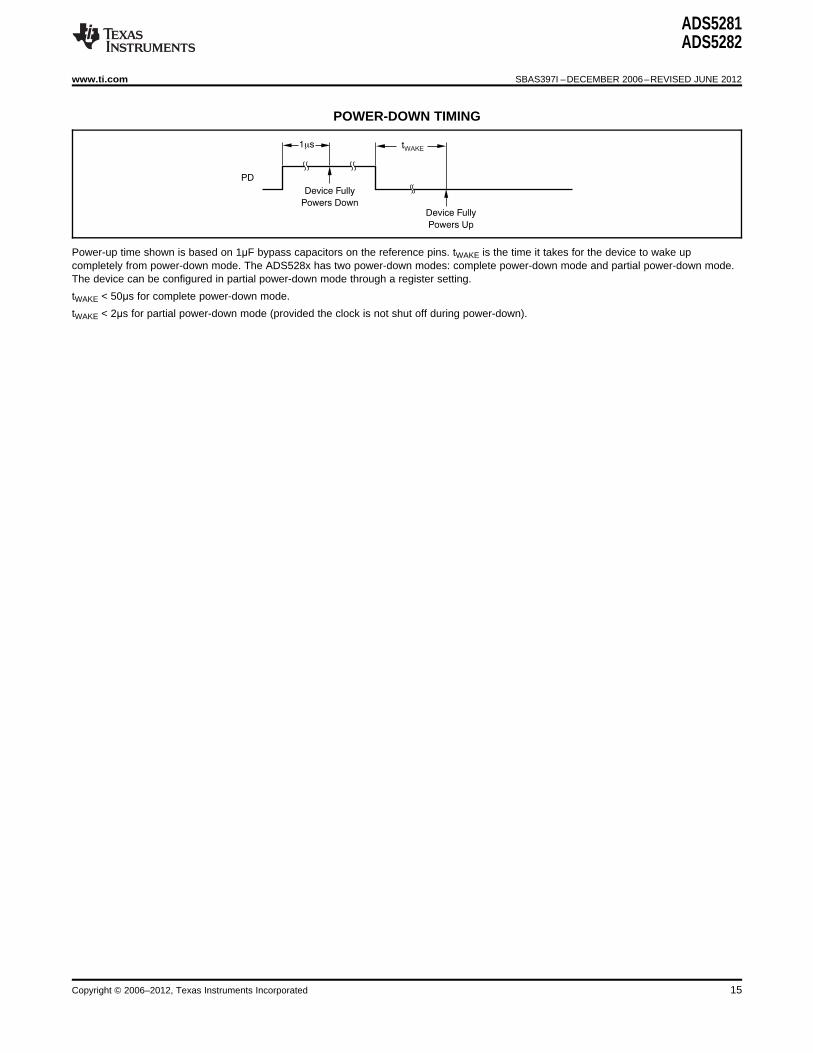
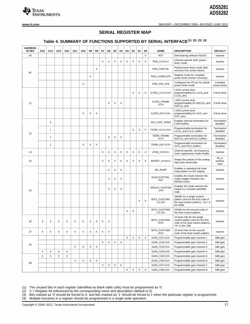
ADS5281ADS5282
wwwticom SBAS397I ndashDECEMBER 2006ndashREVISED JUNE 2012
SERIAL REGISTER MAP
Table 4 SUMMARY OF FUNCTIONS SUPPORTED BY SERIAL INTERFACE (1) (2) (3) (4)
ADDRESSIN HEX D15 D14 D13 D12 D11 D10 D9 D8 D7 D6 D5 D4 D3 D2 D1 D0 NAME DESCRIPTION DEFAULT
00 X RST Self-clearing software RESET Inactive
Channel-specific ADC power-X X X X X X X X PDN_CHlt81gt Inactive
down mode
Partial power-down mode (fastX PDN_PARTIAL Inactive
recovery from power-down)0F
Register mode for completeX PDN_COMPLETE Inactive
power-down (slower recovery)
Configures the PD pin for partial CompleteX PDN_PIN_CFG
power-down mode power-down
LVDS current driveX X X ILVDS_LCLKlt20gt programmability for LCLKN and 35mA drive
LCLKP pins
LVDS current driveILVDS_FRAME
11 X X X programmability for ADCLKN and 35mA drivelt20gt
ADCLKP pins
LVDS current driveX X X ILVDS_DATlt20gt programmability for OUTN and 35mA drive
OUTP pins
Enables internal termination for TerminationX EN_LVDS_TERM
LVDS buffers disabled
Programmable termination for Termination1 X X X TERM_LCLKlt20gt
LCLKN and LCLKP buffers disabled12
TERM_FRAME Programmable termination for Termination1 X X X
lt20gt ADCLKN and ADCLKP buffers disabled
Programmable termination for Termination1 X X X TERM_DATlt20gt
OUTN and OUTP buffers disabled
Channel-specific low-frequency14 X X X X X X X X LFNS_CHlt81gt Inactive
noise suppression mode enable
INP isSwaps the polarity of the analog
24 X X X X X X X X INVERT_CHlt81gt positiveinput pins electrically
input
Enables a repeating full-scaleX 0 0 EN_RAMP Inactive
ramp pattern on the outputs
Enables the mode wherein theDUALCUSTOM_
0 X 0 output toggles between two InactivePAT
defined codes
Enables the mode wherein theSINGLE_CUSTOM
0 0 X output is a constant specified Inactive25 _PAT
code
2MSBs for a single customBITS_CUSTOM1 pattern (and for the first code of
X X Inactivelt1110gt the dual custom pattern) lt11gt is
the MSB
BITS_CUSTOM2 2MSBs for the second code ofX X Inactive
lt1110gt the dual custom pattern
10 lower bits for the singleBITS_CUSTOM1 custom pattern (and for the first
26 X X X X X X X X X X Inactivelt90gt code of the dual custom pattern)
lt0gt is the LSB
BITS_CUSTOM2 10 lower bits for the second27 X X X X X X X X X X Inactive
lt90gt code of the dual custom pattern
X X X X GAIN_CH1lt30gt Programmable gain channel 1 0dB gain
X X X X GAIN_CH2lt30gt Programmable gain channel 2 0dB gain2A
X X X X GAIN_CH3lt30gt Programmable gain channel 3 0dB gain
X X X X GAIN_CH4lt30gt Programmable gain channel 4 0dB gain
X X X X GAIN_CH5lt30gt Programmable gain channel 5 0dB gain
X X X X GAIN_CH6lt30gt Programmable gain channel 6 0dB gain2B
X X X X GAIN_CH7lt30gt Programmable gain channel 7 0dB gain
X X X X GAIN_CH8lt30gt Programmable gain channel 8 0dB gain
(1) The unused bits in each register (identified as blank table cells) must be programmed as 0(2) X = Register bit referenced by the corresponding name and description (default is 0)(3) Bits marked as 0 should be forced to 0 and bits marked as 1 should be forced to 1 when the particular register is programmed(4) Multiple functions in a register should be programmed in a single write operation
Copyright copy 2006ndash2012 Texas Instruments Incorporated 17
ADS5281ADS5282
SBAS397I ndashDECEMBER 2006ndashREVISED JUNE 2012 wwwticom
Table 4 SUMMARY OF FUNCTIONS SUPPORTED BY SERIAL INTERFACE(1) (2) (3) (4) (continued)ADDRESS
IN HEX D15 D14 D13 D12 D11 D10 D9 D8 D7 D6 D5 D4 D3 D2 D1 D0 NAME DESCRIPTION DEFAULT
Single-1 X DIFF_CLK Differential clock mode
ended clock
Enables the duty-cycle correction1 X EN_DCC Disabled
circuit
External42Drives the external reference reference
1 X EXT_REF_VCMmode through the VCM pin drives REFT
and REFB
Controls the phase of LCLK1 X X PHASE_DDRlt10gt 90 degrees
output relative to data
0 X PAT_DESKEW Enables deskew pattern mode Inactive45
X 0 PAT_SYNC Enables sync pattern mode Inactive
Binary twos complement format Straight1 1 X BTC_MODE
for ADC output offset binary
Serialized ADC output comes LSB-first1 1 X MSB_FIRST
out MSB-first output
Enables SDR output modeDDR output46 1 1 X EN_SDR (LCLK becomes a 12x input
modeclock)
Controls whether the LCLK rising Rising edgeor falling edge comes in the of LCLK in
1 X 1 1 FALL_SDRmiddle of the data window when middle ofoperating in SDR output mode data window
SUMMARY OF FEATURES
POWER IMPACT (relative to default)FEATURES DEFAULT SELECTION AT fS = 65MSPS
ANALOG FEATURES
Internal or external reference Internal reference mode uses approximately 23mW moreNA Pin(driven on the REFT and REFB pins) power on AVDD
External reference driven on the Off Register 42 Approximately 9mW less power on AVDDVCM pin
Duty cycle correction circuit Off Register 42 Approximately 7mW more power on AVDD
With zero input to the ADC low-frequency noise suppressionLow-frequency noise suppression Off Register 14 causes digital switching at fS2 thereby increasing LVDD
power by approximately 7mWchannel
Differential clock mode uses approximately 7mW more powerSingle-ended or differential clock Single-ended Register 42 on AVDD
Refer to the Power-Down Modes section in the ElectricalPower-down mode Off Pin and register 0F Characteristics table
DIGITAL FEATURES
Programmable digital gain (0dB to Registers 2A and0dB No difference12dB) 2B
Straight offset or BTC output Straight offset Register 46 No difference
Swap polarity of analog input pins Off Register 24 No difference
LVDS OUTPUT PHYSICAL LAYER
LVDS internal termination Off Register 12 Approximately 7mW more power on AVDD
LVDS current programmability 35mA Register 11 As per LVDS clock and data buffer current setting
LVDS OUTPUT TIMING
LSB- or MSB-first output LSB-first Register 46 No difference
SDR mode uses approximately 2mW more power on LVDDDDR or SDR output DDR Register 46 (at fS = 30MSPS)
Refer toLCLK phase relative to data output Register 42 No differenceFigure 1
18 Copyright copy 2006ndash2012 Texas Instruments Incorporated
ADS5281ADS5282
wwwticom SBAS397I ndashDECEMBER 2006ndashREVISED JUNE 2012
DESCRIPTION OF SERIAL REGISTERS
SOFTWARE RESET
ADDRESSIN HEX D15 D14 D13 D12 D11 D10 D9 D8 D7 D6 D5 D4 D3 D2 D1 D0 NAME
00 X RST
Software reset is applied when the RST bit is set to 1 setting this bit resets all internal registers and self-clearsto 0
POWER-DOWN MODES
ADDRESSIN HEX D15 D14 D13 D12 D11 D10 D9 D8 D7 D6 D5 D4 D3 D2 D1 D0 NAME
X X X X X X X X PDN_CHlt81gt
X PDN_PARTIAL0F
0 X PDN_COMPLETE
X 0 PDN_PIN_CFG
Each of the eight channels can be individually powered down PDN_CHltNgt controls the power-down mode forthe ADC channel ltNgt
In addition to channel-specific power-down the ADS528x also has two global power-down modesmdashpartialpower-down mode and complete power-down mode Partial power-down mode partially powers down the chiprecovery from this mode is much quicker provided that the clock has been running for at least 50μs beforeexiting this mode Complete power-down mode on the other hand completely powers down the chip andinvolves a much longer recovery time
In addition to programming the device for either of these two power-down modes (through either thePDN_PARTIAL or PDN_COMPLETE bits respectively) the PD pin itself can be configured as either a partialpower-down pin or a complete power-down pin control For example if PDN_PIN_CFG = 0 (default) when thePD pin is high the device enters complete power-down mode However if PDN_PIN_CFG = 1 when the PD pinis high the device enters partial power-down mode
LVDS DRIVE PROGRAMMABILITY
ADDRESSIN HEX D15 D14 D13 D12 D11 D10 D9 D8 D7 D6 D5 D4 D3 D2 D1 D0 NAME
X X X ILVDS_LCLKlt20gt
11 X X X ILVDS_FRAMElt20gt
X X X ILVDS_DATlt20gt
The LVDS drive strength of the bit clock (LCLKP or LCLKN) and the frame clock (ADCLKP or ADCLKN) can beindividually programmed The LVDS drive strengths of all the data outputs OUTP and OUTN can also beprogrammed to the same value
Copyright copy 2006ndash2012 Texas Instruments Incorporated 19
ADS5281ADS5282
SBAS397I ndashDECEMBER 2006ndashREVISED JUNE 2012 wwwticom
All three drive strengths (bit clock frame clock and data) are programmed using sets of three bits Table 5shows an example of how the drive strength of the bit clock is programmed (the method is similar for the frameclock and data drive strengths)
Table 5 Bit Clock Drive Strength (1)
ILVDS_LCLKlt2gt ILVDS_LCLKlt1gt ILVDS_LCLKlt0gt LVDS DRIVE STRENGTH FOR LCLKP AND LCLKN
0 0 0 35mA (default)
0 0 1 25mA
0 1 0 15mA
0 1 1 05mA
1 0 0 75mA
1 0 1 65mA
1 1 0 55mA
1 1 1 45mA
(1) Current settings lower than 15mA are not recommended
LVDS INTERNAL TERMINATION PROGRAMMABILITY
ADDRESSIN HEX D15 D14 D13 D12 D11 D10 D9 D8 D7 D6 D5 D4 D3 D2 D1 D0 NAME
X EN_LVDS_TERM
1 X X X TERM_LCLKlt20gt12
1 X X X TERM_FRAMElt20gt
1 X X X TERM_DATlt20gt
The LVDS buffers have high-impedance current sources driving the outputs When driving traces whosecharacteristic impedance is not perfectly matched with the termination impedance on the receiver side there maybe reflections back to the LVDS output pins of the ADS528x that cause degraded signal integrity By enabling aninternal termination (between the positive and negative outputs) for the LVDS buffers the signal integrity can besignificantly improved in such scenarios To set the internal termination mode the EN_LVDS_TERM bit shouldbe set to 1 Once this bit is set the internal termination values for the bit clock frame clock and data bufferscan be independently programmed using sets of three bits Table 6 shows an example of how the internaltermination of the LVDS buffer driving the bit clock is programmed (the method is similar for the frame clock anddata buffers) These termination values are only typical values and can vary by up to plusmn20 across temperatureand from device to device
Table 6 Bit Clock Internal Termination
INTERNAL TERMINATION BETWEENTERM_LCLKlt2gt TERM_LCLKlt1gt TERM_LCLKlt0gt LCLKP AND LCLKN IN Ω
0 0 0 None
0 0 1 260
0 1 0 150
0 1 1 94
1 0 0 125
1 0 1 80
1 1 0 66
1 1 1 55
20 Copyright copy 2006ndash2012 Texas Instruments Incorporated
ADS5281ADS5282
wwwticom SBAS397I ndashDECEMBER 2006ndashREVISED JUNE 2012
LOW-FREQUENCY NOISE SUPPRESSION MODE
ADDRESSIN HEX D15 D14 D13 D12 D11 D10 D9 D8 D7 D6 D5 D4 D3 D2 D1 D0 NAME
14 X X X X X X X X LFNS_CHlt81gt
The low-frequency noise suppression mode is specifically useful in applications where good noise performance isdesired in the frequency band of 0MHz to 1MHz (around dc) Setting this mode shifts the low-frequency noise ofthe ADS528x to approximately fS2 thereby moving the noise floor around dc to a much lower valueLFNS_CHlt81gt enables this mode individually for each channel
ANALOG INPUT INVERT
ADDRESSIN HEX D15 D14 D13 D12 D11 D10 D9 D8 D7 D6 D5 D4 D3 D2 D1 D0 NAME
24 X X X X X X X X INVERT_CHlt81gt
Normally the INP pin represents the positive analog input pin and INN represents the complementary negativeinput Setting the bits marked INVERT_CHlt81gt (individual control for each channel) causes the inputs to beswapped INN now represents the positive input and INP the negative input
LVDS TEST PATTERNS
ADDRESSIN HEX D15 D14 D13 D12 D11 D10 D9 D8 D7 D6 D5 D4 D3 D2 D1 D0 NAME
X 0 0 EN_RAMP
0 X 0 DUALCUSTOM_PAT
25 0 0 X SINGLE_CUSTOM_PAT
X X BITS_CUSTOM1lt1110gt
X X BITS_CUSTOM2lt1110gt
26 X X X X X X X X X X BITS_CUSTOM1lt90gt
27 X X X X X X X X X X BITS_CUSTOM2lt90gt
0 X PAT_DESKEW45
X 0 PAT_SYNC
The ADS528x can output a variety of test patterns on the LVDS outputs These test patterns replace the normalADC data output Setting EN_RAMP to 1 causes all the channels to output a repeating full-scale ramp patternThe ramp increments from zero code to full-scale code in steps of 1LSB every clock cycle After hitting the full-scale code it returns back to zero code and ramps again
The device can also be programmed to output a constant code by setting SINGLE_CUSTOM_PAT to 1 andprogramming the desired code in BITS_CUSTOM1lt110gt In this mode BITS_CUSTOM1lt110gt take the placeof the 12-bit ADC data at the output and are controlled by LSB-first and MSB-first modes in the same way asnormal ADC data are
The device may also be made to toggle between two consecutive codes by programming DUAL_CUSTOM_PATto 1 The two codes are represented by the contents of BITS_CUSTOM1lt110gt and BITS_CUSTOM2lt110gt
In addition to custom patterns the device may also be made to output two preset patterns1 Deskew patten Set using PAT_DESKEW this mode replaces the 12-bit ADC output Dlt110gt with the
010101010101 word2 Sync pattern Set using PAT_SYNC the normal ADC word is replaced by a fixed 111111000000 word
Note that only one of the above patterns should be active at any given instant
Copyright copy 2006ndash2012 Texas Instruments Incorporated 21
ADS5281ADS5282
SBAS397I ndashDECEMBER 2006ndashREVISED JUNE 2012 wwwticom
PROGRAMMABLE GAIN
ADDRESSIN HEX D15 D14 D13 D12 D11 D10 D9 D8 D7 D6 D5 D4 D3 D2 D1 D0 NAME
X X X X GAIN_CH1lt30gt
X X X X GAIN_CH2lt30gt2A
X X X X GAIN_CH3lt30gt
X X X X GAIN_CH4lt30gt
X X X X GAIN_CH5lt30gt
X X X X GAIN_CH6lt30gt2B
X X X X GAIN_CH7lt30gt
X X X X GAIN_CH8lt30gt
In applications where the full-scale swing of the analog input signal is much less than the 2VPP range supportedby the ADS528x a programmable gain can be set to achieve the full-scale output code even with a lower analoginput swing The programmable gain not only fills the output code range of the ADC but also enhances the SNRof the device by utilizing quantization information from some extra internal bits The programmable gain for eachchannel can be individually set using a set of four bits indicated as GAIN_CHNlt30gt for Channel N The gainsetting is coded in binary from 0dB to 12dB as shown in Table 7
Table 7 Gain Setting for Channel 1
GAIN_CH1lt3gt GAIN_CH1lt2gt GAIN_CH1lt1gt GAIN_CH1lt0gt CHANNEL 1 GAIN SETTING
0 0 0 0 0dB
0 0 0 1 1dB
0 0 1 0 2dB
0 0 1 1 3dB
0 1 0 0 4dB
0 1 0 1 5dB
0 1 1 0 6dB
0 1 1 1 7dB
1 0 0 0 8dB
1 0 0 1 9dB
1 0 1 0 10dB
1 0 1 1 11dB
1 1 0 0 12dB
1 1 0 1 Do not use
1 1 1 0 Do not use
1 1 1 1 Do not use
22 Copyright copy 2006ndash2012 Texas Instruments Incorporated
VREF = 15V -B
VCM
15V
VREF = 15V +T
VCM
15V
ADS5281ADS5282
wwwticom SBAS397I ndashDECEMBER 2006ndashREVISED JUNE 2012
CLOCK REFERENCE AND DATA OUTPUT MODES
ADDRESSIN HEX D15 D14 D13 D12 D11 D10 D9 D8 D7 D6 D5 D4 D3 D2 D1 D0 NAME
1 X DIFF_CLK
1 X EN_DCC42
1 X EXT_REF_VCM
1 X X PHASE_DDRlt10gt
1 1 X BTC_MODE
1 1 X MSB_FIRST46
1 1 X EN_SDR
1 X 1 1 FALL_SDR
INPUT CLOCK
The ADS528x is configured by default to operate with a single-ended input clockmdashCLKP is driven by a CMOSclock and CLKN is tied to 0 However by programming DIFF_CLK to 1 the device can be made to work with adifferential input clock on CLKP and CLKN Operating with a low-jitter differential clock usually gives better SNRperformance especially at input frequencies greater than 30MHz
In cases where the duty cycle of the input clock falls outside the 45 to 55 range it is recommended to enablean internal duty cycle correction circuit This enabling is done by setting the EN_DCC bit to 1
EXTERNAL REFERENCE
The ADS528x can be made to operate in external reference mode by pulling the INTEXT pin to 0 In this modethe REFT and REFB pins should be driven with voltage levels of 25V and 05V respectively and must haveenough drive strength to drive the switched capacitance loading of the reference voltages by each ADC Theadvantage of using the external reference mode is that multiple ADS528x units can be made to operate with thesame external reference thereby improving parameters such as gain matching across devices However inapplications that do not have an available high drive differential external reference the ADS528x can still bedriven with a single external reference voltage on the VCM pin When EXT_REF_VCM is set as 1 (and theINTEXT pin is set to 0) the VCM pin is configured as an input pin and the voltages on REFT and REFB aregenerated as shown in Equation 1 and Equation 2
(1)
(2)
Copyright copy 2006ndash2012 Texas Instruments Incorporated 23
PHASE_DDRlt10gt = 00
PHASE_DDRlt10gt = 01
PHASE_DDRlt10gt = 10
PHASE_DDRlt10gt = 11
ADCLKP
LCLKP
OUTP
ADCLKP
LCLKP
OUTP
ADCLKP
LCLKP
OUTP
ADCLKP
LCLKP
OUTP
ADCLKP
LCLKP
OUTP
ADS5281ADS5282
SBAS397I ndashDECEMBER 2006ndashREVISED JUNE 2012 wwwticom
BIT CLOCK PROGRAMMABILITY
The output interface of the ADS528x is normally a DDR interface with the LCLK rising edge and falling edgetransitions in the middle of alternate data windows This default phase is shown in Figure 1
Figure 1 Default Phase of LCLK
The phase of LCLK can be programmed relative to the output frame clock and data using bitsPHASE_DDRlt10gt The LCLK phase modes are shown in Figure 2
Figure 2 Phase Programmability Modes for LCLK
24 Copyright copy 2006ndash2012 Texas Instruments Incorporated
EN_SDR = 1 FALL_SDR = 0
EN_SDR = 1 FALL_SDR = 1
ADCLKP
LCLKP
OUTP
ADCLKP
LCLKP
OUTP
ADS5281ADS5282
wwwticom SBAS397I ndashDECEMBER 2006ndashREVISED JUNE 2012
In addition to programming the phase of LCLK in the DDR mode the device can also be made to operate in SDRmode by setting the EN_SDR bit to 1 In this mode the bit clock (LCLK) is output at 12x times the input clock ortwice the rate as in DDR mode Depending on the state of FALL_SDR LCLK may be output in either of the twomanners shown in Figure 3 As can be seen in Figure 3 only the LCLK rising (or falling) edge is used to capturethe output data in SDR mode
Figure 3 SDR Interface Modes
The SDR mode does not work well beyond 40MSPS because the LCLK frequency becomes very high
DATA OUTPUT FORMAT MODES
The ADC output by default is in straight offset binary mode Programming the BTC_MODE bit to 1 inverts theMSB and the output becomes binary twos complement mode
Also by default the first bit of the frame (following the rising edge of ADCLKP) is the LSB of the ADC outputProgramming the MSB_FIRST mode inverts the bit order in the word and the MSB is output as the first bitfollowing the ADCLKP rising edge
Copyright copy 2006ndash2012 Texas Instruments Incorporated 25
0
-
-
-
-
-
-
-
-
-
20
40
60
80
100
120
140
160
180
Input Frequency (MHz)
0 25
Am
plit
ude (
dB
)
2015105
SFDR = 884dBc
SNR = 709dBFS
SINAD = 708dBFS
THD = 875dBc
0
-
-
-
-
-
-
-
-
-
20
40
60
80
100
120
140
160
180
Input Frequency (MHz)
0 25
Am
plit
ude (
dB
)
2015105
SFDR = 856dBc
SNR = 705dBFS
SINAD = 704dBFS
THD = 839dBc
0
-
-
-
-
-
-
-
-
-
20
40
60
80
100
120
140
160
180
Input Frequency (MHz)
0 2 20
Am
plit
ude (
dB
)
1816141210864
SFDR = 853dBc
SNR = 708dBFS
SINAD = 707dBFS
THD = 893dBc
0
-
-
-
-
-
-
-
-
-
20
40
60
80
100
120
140
160
180
Input Frequency (MHz)
0 2 20
Am
plit
ude (
dB
)
1816141210864
SFDR = 828dBc
SNR = 702dBFS
SINAD = 70dBFS
THD = 823dBc
ADS5281ADS5282
SBAS397I ndashDECEMBER 2006ndashREVISED JUNE 2012 wwwticom
TYPICAL CHARACTERISTICSAt TA = +25degC AVDD = +33V LVDD = 18V clock frequency = 65MSPS differential clock mode 1VPP clock amplitude 50
clock duty cycle input frequency = 10MHz ndash1dBFS differential analog input 0dB digital gain setting 15V analog inputcommon-mode low-frequency noise suppression = off internal reference mode ISET resistor = 562kΩ and LVDS buffer
current setting = 35mA unless otherwise noted
SPECTRAL PERFORMANCE SPECTRAL PERFORMANCE(fS = 40MHz fIN = 10MHz) (fS = 40MHz fIN = 25MHz)
Figure 4 Figure 5
SPECTRAL PERFORMANCE SPECTRAL PERFORMANCE(fS = 50MHz fIN = 10MHz) (fS = 50MHz fIN = 25MHz)
Figure 6 Figure 7
26 Copyright copy 2006ndash2012 Texas Instruments Incorporated
0
-20
-40
-60
-80
-100
-120
-140
-180
Input Frequency (MHz)
0 33
Am
plit
ude (
dB
)
2015105
-160
SFDR = 862dBc
SNR = 705dBFS
SNR (0MHz to 1MHz) = 861dBFS
SINAD = 704dBFS
THD = 854dBc
25 30
92
87
82
77
72
67
Input Frequency (MHz)
5 30
Dynam
ic P
erf
orm
ance (
SN
R S
FD
R)
201510 25
SNR (dBFS)
SFDR (dBc)
f = 40MHzS
0
-
-
-
-
-
-
-
-
-
20
40
60
80
100
120
140
160
180
Input Frequency (MHz)
0 33
Am
plit
ude (
dB
)
2015105 25 30
SFDR = 909dBc
SNR = 708dBFS
SINAD = 707dBFS
THD = 904dBc
0
-20
-40
-60
-80
-100
-120
-140
-180
Input Frequency (MHz)
0 33
Am
plit
ude (
dB
)
2015105
-160
SFDR = 874dBc
SNR = 704dBFS
SNR (0MHz to 1MHz) = 819dBFS
SINAD = 703dBFS
THD = 864dBc
25 30
ADS5281ADS5282
wwwticom SBAS397I ndashDECEMBER 2006ndashREVISED JUNE 2012
TYPICAL CHARACTERISTICS (continued)At TA = +25degC AVDD = +33V LVDD = 18V clock frequency = 65MSPS differential clock mode 1VPP clock amplitude 50clock duty cycle input frequency = 10MHz ndash1dBFS differential analog input 0dB digital gain setting 15V analog inputcommon-mode low-frequency noise suppression = off internal reference mode ISET resistor = 562kΩ and LVDS buffercurrent setting = 35mA unless otherwise noted
SPECTRAL PERFORMANCE SPECTRAL PERFORMANCE(fS = 65MHz fIN = 10MHz) (fS = 65MHz fIN = 25MHz)
Figure 8 Figure 9
SPECTRAL PERFORMANCE LOW-FREQUENCY NOISESUPPRESSION MODE ENABLED
(fS = 65MHz fIN = 25MHz) DYNAMIC PERFORMANCE vs INPUT FREQUENCY
Figure 10 Figure 11
Copyright copy 2006ndash2012 Texas Instruments Incorporated 27
95
85
75
65
55
45
35
25
Input Amplitude (dBFS)
Dyn
am
ic P
erf
orm
an
ce
(S
NR
S
FD
R)
SNR (dBFS)
SFDR (dBc)
f = 65MHz
f = 10MHzS
IN
-60 0-50 -40 -30 -20 -10
94
89
84
79
74
69
Clock Amplitude (V Differential)PP
06 23
Dynam
ic P
erf
orm
ance (
SN
R S
FD
R)
1611
SNR (dBFS)
SFDR (dBc)
f = 65MHz
f = 10MHzS
IN
21
95
90
85
80
75
70
65
60
Digital Gain (dB)
0 12
Dyn
am
ic P
erf
orm
an
ce
(S
NR
S
FD
R)
642 8
SNR (dBFS)
SFDR (dBc)
f = 65MHz
f = 10MHzS
IN
10
95
90
85
80
75
70
65
60
AVDD (V)
30 36
Dynam
ic P
erf
orm
ance (
SN
R S
FD
R)
333231 34
SNR (dBFS)
SFDR (dBc)
f = 65MHz
f = 10MHzS
IN
35
92
87
82
77
72
67
Input Frequency (MHz)
5 30
Dynam
ic P
erf
orm
ance (
SN
R S
FD
R)
201510 25
SNR (dBFS)
SFDR (dBc)
f = 50MHzS
97
92
87
82
77
72
67
Input Frequency (MHz)
5 30
Dynam
ic P
erf
orm
ance (
SN
R S
FD
R)
201510 25
SNR (dBFS)
SFDR (dBc)
f = 65MHzS
ADS5281ADS5282
SBAS397I ndashDECEMBER 2006ndashREVISED JUNE 2012 wwwticom
TYPICAL CHARACTERISTICS (continued)At TA = +25degC AVDD = +33V LVDD = 18V clock frequency = 65MSPS differential clock mode 1VPP clock amplitude 50clock duty cycle input frequency = 10MHz ndash1dBFS differential analog input 0dB digital gain setting 15V analog inputcommon-mode low-frequency noise suppression = off internal reference mode ISET resistor = 562kΩ and LVDS buffercurrent setting = 35mA unless otherwise noted
DYNAMIC PERFORMANCE vs INPUT FREQUENCY DYNAMIC PERFORMANCE vs INPUT FREQUENCY
Figure 12 Figure 13
DYNAMIC PERFORMANCE vs DIGITAL GAIN DYNAMIC PERFORMANCE vs AVDD
Figure 14 Figure 15
DYNAMIC PERFORMANCE vs INPUT AMPLITUDE DYNAMIC PERFORMANCE vs CLOCK AMPLITUDE
Figure 16 Figure 17
28 Copyright copy 2006ndash2012 Texas Instruments Incorporated
94
89
84
79
74
69
External Reference Common-Mode Voltage (REF + REF )2 (V)T B
135 165
Dynam
ic P
erf
orm
ance (
SN
R S
FD
R)
150145140
SNR (dBFS)
SFDR (dBc)
f = 65MHz
f = 10MHzS
IN
155 160
External reference differential voltage maintained at 2V
94
89
84
79
74
69
Voltage on V (V)CM
135 165
Dynam
ic P
erf
orm
ance (
SN
R S
FD
R)
150145140
SNR (dBFS)
SFDR (dBc)
f = 65MHz
f = 10MHzS
IN
155 160
94
89
84
79
74
69
Analog Input Common-Mode Voltage (V)
130 170
Dynam
ic P
erf
orm
ance (
SN
R S
FD
R)
140135
SNR (dBFS)
SFDR (dBc)
f = 65MHz
f = 10MHzS
IN
145 165160155150
94
89
84
79
74
69
External Reference Differential Voltage REF REF (V)-T B
16 24
Dynam
ic P
erf
orm
ance (
SN
R S
FD
R)
191817
SNR (dBFS)
SFDR (dBc)
f = 65MHz
f = 10MHzS
IN
20 232221
External reference common-mode voltage
maintained at 15V
ADS5281ADS5282
wwwticom SBAS397I ndashDECEMBER 2006ndashREVISED JUNE 2012
TYPICAL CHARACTERISTICS (continued)At TA = +25degC AVDD = +33V LVDD = 18V clock frequency = 65MSPS differential clock mode 1VPP clock amplitude 50clock duty cycle input frequency = 10MHz ndash1dBFS differential analog input 0dB digital gain setting 15V analog inputcommon-mode low-frequency noise suppression = off internal reference mode ISET resistor = 562kΩ and LVDS buffercurrent setting = 35mA unless otherwise noted
DYNAMIC PERFORMANCE vs ANALOG INPUT COMMON- DYNAMIC PERFORMANCE vs EXTERNAL REFERENCEMODE VOLTAGE DIFFERENTIAL VOLTAGE
Figure 18 Figure 19
DYNAMIC PERFORMANCE vs EXTERNAL REFERENCE DYNAMIC PERFORMANCE vs EXTERNAL REFERENCECOMMON-MODE VOLTAGE FORCED THROUGH VCM
Figure 20 Figure 21
Copyright copy 2006ndash2012 Texas Instruments Incorporated 29
05
04
03
02
01
0
-01
-02
-05
Code (LSB)
0 4096
INL
(L
SB
)
30722048 25601536 35841024512
-04
-03
f = 50MSPS
f = 5MHzS
IN
035
025
015
005
-005
-015
-035
Code (LSB)
0 4096
DN
L (
LS
B)
30722048 25601536 35841024512
-025
f = 50MSPS
f = 5MHzS
IN
60
50
40
30
20
10
0
Code Bin (LSB)
2049
Occurr
ence (
)
20532051 2054
f = 65MSPSS
2050 2052
0 0037 028
5192
4743
10
-10
-30
-50
-70
-90
-110
-130
-150
Input Frequency (MHz)
0 2 20
Am
plit
ude (
dB
)
1816141210864
f = 65MHz
f = 10MHz ( 7dBFS)
f = 161MHz ( 7dBFS)
IMD = 97dBFS
-
-
-
S
1
2
95
90
85
80
75
70
65
60
Clock Duty Cycle ()
35 65
Dynam
ic P
erf
orm
ance (
SN
R S
FD
R)
504540 55
SNR (dBFS)
SFDR (dBc)
f = 65MHz
f = 10MHzS
IN
60
95
85
80
75
70
60
Clock Duty Cycle ()
20 80
Dynam
ic P
erf
orm
ance (
SN
R S
FD
R)
504030 60
SNR (dBFS)
SFDR (dBc)
f = 65MHz
f = 10MHzS
IN
90
70
65
ADS5281ADS5282
SBAS397I ndashDECEMBER 2006ndashREVISED JUNE 2012 wwwticom
TYPICAL CHARACTERISTICS (continued)At TA = +25degC AVDD = +33V LVDD = 18V clock frequency = 65MSPS differential clock mode 1VPP clock amplitude 50clock duty cycle input frequency = 10MHz ndash1dBFS differential analog input 0dB digital gain setting 15V analog inputcommon-mode low-frequency noise suppression = off internal reference mode ISET resistor = 562kΩ and LVDS buffercurrent setting = 35mA unless otherwise noted
DYNAMIC PERFORMANCE vs CLOCK DUTY CYCLE DCC DYNAMIC PERFORMANCE vs CLOCK DUTY CYCLE DCCDISABLED ENABLED
Figure 22 Figure 23
HISTOGRAM OF OUTPUT CODE FOR ZERO INPUT INTERMODULATION DISTORTION
Figure 24 Figure 25
INTEGRAL NONLINEARITY DIFFERENTIAL NONLINEARITY
Figure 26 Figure 27
30 Copyright copy 2006ndash2012 Texas Instruments Incorporated
064
062
060
058
056
054
052
Sta
ndard
Devia
tion (
LS
B)
0 1 2 3 4 5 6
Overload Signal Amplitude (dBFS)
f = 65MSPS
f = 5MHzS
IN
Standard Deviation of
2nd Point After Overload
Standard Deviation of
1st Point After Overload
tS
16384 t (Group 1)S
Set 1 Point 1 (of 16) Set 1 Point 2 (of 16)
First point after overload (Set 1)
First point after overload (Set 2)
Second point after overload (Set 2)
Second point after overload (Set 1)
Overload
Amplitude
NOTES
Input sine wave phase is repetitive over 16384 clock cycles
16 such repetitive groups (of 16384 clock cycles) are capturedndasha total of 262144 points
Standard deviation of every set of are analyzed over the 16 groups
Worst case of all such standard deviations are plotted in the graphs
first and second points after overload
+FS
-FS
070
068
066
064
062
060
058
056
054
052
050
Sta
nd
ard
De
via
tio
n (
in L
SB
)
0 1 2 3 4 5 6
Overload Signal Amplitude (dBFS)
f = 50MSPS
f = 5MHzS
IN Standard Deviation of
2nd Point After Overload
Standard Deviation of
1st Point After Overload
170
130
110
90
70
30
Clock Frequency (MSPS)
5 75
I I
(mA
)A
VD
DLV
DD
352515 45
ILVDD
IAVDD
Zero Input on All Channels
Internal Reference Mode150
55
50
65
075
055
035
015
-005
-025
-065
Code (LSB)
0 4096
INL
(LS
B)
30722048 25601536 35841024512
-045
f = 65MSPS
f = 5MHzS
IN
035
025
015
005
-005
-015
-035
Code (LSB)
0 4096
DN
L (
LS
B)
30722048 25601536 35841024512
-025
f = 65MSPS f = 5MHzS IN
ADS5281ADS5282
wwwticom SBAS397I ndashDECEMBER 2006ndashREVISED JUNE 2012
TYPICAL CHARACTERISTICS (continued)At TA = +25degC AVDD = +33V LVDD = 18V clock frequency = 65MSPS differential clock mode 1VPP clock amplitude 50clock duty cycle input frequency = 10MHz ndash1dBFS differential analog input 0dB digital gain setting 15V analog inputcommon-mode low-frequency noise suppression = off internal reference mode ISET resistor = 562kΩ and LVDS buffercurrent setting = 35mA unless otherwise noted
INTEGRAL NONLINEARITY DIFFERENTIAL NONLINEARITY
Figure 28 Figure 29
AVDD AND LVDD POWER-SUPPLY CURRENTSvs CLOCK FREQUENCY OVERLOAD RECOVERY AT 50MSPS
Figure 30 Figure 31
OVERLOAD RECOVERY AT 65MSPS
Figure 32 Figure 33 Overload Recovery
Copyright copy 2006ndash2012 Texas Instruments Incorporated 31
ADS5281ADS5282
SBAS397I ndashDECEMBER 2006ndashREVISED JUNE 2012 wwwticom
APPLICATION INFORMATION
The ADC output goes to a serializer that operatesTHEORY OF OPERATION from a 12x clock generated by the PLL The 12 databits from each channel are serialized and sent LSBThe ADS528x devices are a family of 8-channelfirst In addition to serializing the data the serializerhigh-speed CMOS ADCs The 12 bits given out byalso generates a 1x clock and a 6x clock Theseeach channel are serialized and sent out on a singleclocks are generated in the same way the serializedpair of pins in LVDS format All eight channels of thedata are generated so these clocks maintain perfectADS528x operate from a single clock (ADCLK) Thesynchronization with the data The data and clocksampling clocks for each of the eight channels areoutputs of the serializer are buffered externally usinggenerated from the input clock using a carefullyLVDS buffers Using LVDS buffers to transmit datamatched clock buffer tree The 12x clock required forexternally has multiple advantages such as athe serializer is generated internally from ADCLKreduced number of output pins (saving routing spaceusing a phase-locked loop (PLL) A 6x and a 1x clockon the board) reduced power consumption andare also output in LVDS format along with the datareduced effects of digital noise coupling to the analogto enable easy data capture The ADS528x operatescircuit inside the ADS528xfrom internally-generated reference voltages that are
trimmed to improve to a high level of accuracy The ADS528x operates from two sets of supplies andTrimmed references improve the gain matching grounds The analog supply and ground set isacross devices and provide the option to operate the identified as AVDD and AVSS while the digital set isdevices without having to externally drive and route identified by LVDD and LVSSreference lines The nominal values of REFT andREFB are 25V and 05V respectively The ANALOG INPUTreferences are internally scaled down differentially bya factor of 2 This scaling results in a differential input The analog input consists of a switched-capacitorof ndash1V to correspond to the zero code of the ADC based differential sample-and-hold architecture Thisand a differential input of +1V to correspond to the differential topology results in very good acfull-scale code (4095 LSB) VCM (the common-mode performance even for high input frequencies at highvoltage of REFT and REFB) is also made available sampling rates The INN and INP pins must beexternally through a pin and is nominally 15V externally biased around a common-mode voltage of
15V available on VCM For a full-scale differentialThe ADC employs a pipelined converter architectureinput each input pin (INN and INP) must swingthat consists of a combination of multi-bit and single-symmetrically between VCM + 05V and VCM ndash 05Vbit internal stages Each stage feeds its data into theresulting in a 2VPP differential input swing Thedigital error correction logic ensuring excellentmaximum input peak-to-peak differential swing isdifferential linearity and no missing codes at the 12-determined to be the difference between the internalbit levelreference voltages REFT (25V nominal) and REFB(05V nominal) Figure 34 illustrates the model of theinput driving circuit
32 Copyright copy 2006ndash2012 Texas Instruments Incorporated
CM Buffer
Internal
Voltage
Reference
Input
Circuitry
INP
INN
VCM
12kW
12kW
ADS528x
(2mA) facute S
50MSPS
5nH to 9nH (TQFP-80)
2nH to 3nH (QFN-64)
15pF
to 24pF
IN OUT
INP
15pF to
25pF
1W
1000W
to 1440W
5W
to 10W
1000W
to 1440W
5nH to 9nH (TQFP-80)
2nH to 3nH (QFN-64)
INN
15pF to
25pF
1W
15W
to 25W
15W
to 30W
02pF
to 03pF
IN OUT
15pF
to 24pF
IN OUT
5W
to 10W
15W
to 25W
15W
to 30W
IN OUT
IN
OUT
16 to 32W W
IN OUT
IN OUT
OUTP
OUTN
Switches that are ON
in SAMPLE phase
Switches that are ON
in HOLD phase
ADS5281ADS5282
wwwticom SBAS397I ndashDECEMBER 2006ndashREVISED JUNE 2012
Figure 34 Analog Input Circuit Model
during ac-coupling by increasing VCM by roughlyInput Common-Mode Current 75mV When operating above 50MSPS it is
recommended that additional parallel resistors beThe input stage of all eight ADCs together sinks aadded externally to restore the input common-modecommon-mode current on the order of 2mA atto at least 14V if the inputs are to be ac-coupled50MSPS Equation 3 describes the dependency of
the common-mode current and the samplingfrequency
(3)
If the driving stage is dc-coupled to the inputs thenEquation 3 can be used to determine its common-mode drive capability and impedance The inputs canalso be ac-coupled to the INN and INP pins In thatcase the input common-mode is set by two internal12kΩ resistors connecting the input pins to VCM Thisarchitecture is shown in Figure 35
When the inputs are ac-coupled there is a drop inthe voltages at INP and INN relative to VCM This can Dashed area denotes one of eight channelsbe computed from Equation 3 At 50MSPS for
Figure 35 Common-Mode Biasing of Input Pinsexample the drop at each of the 16 input pins is150mV which is not optimal for ADC operationInitialization Registers 1 and 5 described in theInitialization Registers table can be used to partiallyreduce the effect of this input common-mode drop
Copyright copy 2006ndash2012 Texas Instruments Incorporated 33
01 Fm 50W
50W
200W
200W
INP
VCM
INN
01 Fm
12 21
47W
47W
01 Fm
01 Fm
25W
25W
11
INP
VCM
INN
ADS5281ADS5282
SBAS397I ndashDECEMBER 2006ndashREVISED JUNE 2012 wwwticom
Driving Circuit At high input frequencies the mismatch in thetransformer parasitic capacitance (between theFor optimum performance the analog inputs must bewindings) results in degraded even-order harmonicdriven differentially This approach improves theperformance Connecting two identical RFcommon-mode noise immunity and even-ordertransformers back-to-back helps to minimize thisharmonic rejection Input configurations using RFmismatch and good performance is obtained fortransformers suitable for low and high inputhigh-frequency input signals An additionalfrequencies are shown in Figure 36 and Figure 37termination resistor pair is required between the tworespectively The single-ended signal is fed to thetransformers as shown in Figure 37 The center pointprimary winding of the RF transformer Theof this termination is connected to ground to improvetransformer is terminated by 50Ω resistor on thethe balance between the positive and negative sidessecondary side Placing the termination on theThe values of the terminations between thesecondary side helps to shield the kicks caused bytransformers and on the secondary side must bethe input sampling capacitors from the RFchosen to achieve an overall 50Ω (in the case of 50Ωtransformer leakage inductances The termination issource impedance)accomplished by two 25Ω resistors connected in
series with the center point connected to the 15Vcommon-mode The 47Ω resistor in series with eachinput pin is required to damp the ringing caused bythe device package parasitics
Figure 36 Drive Circuit at Low Input Frequencies
Figure 37 Drive Circuit at High Input Frequencies
34 Copyright copy 2006ndash2012 Texas Instruments Incorporated
CLKP
CLKN
CMOS Clock Input
01 Fm
01 Fm
CLKP
CLKN
CMOS Single-Ended
Clock
0V
CLKP
CLKN
Differential Sine-Wave
PECL or LVDS Clock Input
01 Fm
01 Fm
5kW 5kW
VCM
CLKP
CLKN
VCM
ADS5281ADS5282
wwwticom SBAS397I ndashDECEMBER 2006ndashREVISED JUNE 2012
CLOCK INPUT
The eight channels on the device operate from asingle ADCLK input To ensure that the aperturedelay and jitter are the same for all channels a clocktree network is used to generate individual samplingclocks to each channel The clock paths for all thechannels are matched from the source point to thesampling circuit This architecture ensures that theperformance and timing for all channels are identicalThe use of the clock tree for matching introduces anaperture delay that is defined as the delay betweenthe rising edge of ADCLK and the actual instant ofsampling The aperture delays for all the channelsare matched to the best possible extent A mismatchof plusmn20ps (plusmn3σ) could exist between the apertureinstants of the eight ADCs within the same chip Figure 39 Internal Clock BufferHowever the aperture delays of ADCs across twodifferent chips can be several hundred picosecondsapart
The ADS528x can be made to operate either inCMOS single-ended clock mode (default isDIFF_CLK = 0) or differential clock mode (SINELVPECL or LVDS) When operating in the single-ended clock mode CLKN must be forced to 0VDCand the single-ended CMOS applied on the CLKP pinThis operation is shown in Figure 38
Figure 40 Differential Clock Driving Circuit(DIFF_CLK = 1)
Figure 38 Single-Ended Clock Driving Circuit(DIFF_CLK = 0)
When configured to operate in the differential clock Figure 41 Single-Ended Clock Driving Circuitmode (register bit DIFF_CLK = 1) the ADS528x clock When DIFF_CLK = 1inputs can be driven differentially (SINE LVPECL orLVDS) with little or no difference in performance
For best performance the clock inputs must bebetween them or with a single-ended (LVCMOS)driven differentially in order to reduce susceptibility toThe common-mode voltage of the clock inputs is setcommon-mode noise For high input frequencyto VCM using internal 5kΩ resistors as shown insampling it is recommended to use a clock sourceFigure 39 This method allows using transformer-with very low jitter Bandpass filtering of the clockcoupled drive circuits for a sine wave clock or ac-source can help reduce the effect of jitter If the dutycoupling for LVPECL and LVDS clock sources ascycle deviates from 50 by more than 2 or 3 it isshown in Figure 40 When operating in the differentialrecommended to enable the DCC through register bitclock mode the single-ended CMOS clock can be ac-EN_DCCcoupled to the CLKP input with CLKN (pin 11)
connected to ground with a 01μF capacitor asshown in Figure 41
Copyright copy 2006ndash2012 Texas Instruments Incorporated 35
Threshold 1 Threshold 2 Threshold 3
10 MHz 45 MHz 65 MHz
Sampling Frequency
ADS5281ADS5282
SBAS397I ndashDECEMBER 2006ndashREVISED JUNE 2012 wwwticom
PLL OPERATION ACROSS SAMPLING Step 2 Disable the PLL automatic switch and setFREQUENCY the PLL configuration depending on the clock
frequencyThe ADS528X uses a PLL for generating the highspeed bit clock (LCLK) the frame clock (ADCLK) amp SAMPLE CLOCK FREQUENCY REGISTER SETTING (Hex)internal clocks for the serializer operation RANGE (MSPS)
Min Max Address DataTo enable operation across the entire frequencyrange the PLL is automatically configured to one of 10 25 E3 0060four states depending on the sampling clock 15 45 E3 00A0frequency range The frequency range detection isautomatic and each time the sampling frequency With the above settings applied for the respectivecrosses a threshold the PLL changes its frequency ranges the part will continue toconfiguration to a new state To prevent unwanted operate as per the stated datasheet specificationstoggling of PLL state around a threshold the circuit for all timing parameters at all specifiedhas an inbuilt hysteresis The ADS528x has three frequencies EXCEPT for the timing specificationsthresholds ndash taking into account the hysteresis range at 40MSPS At 40MSPS the affected parametersof each threshold variation across devices and are ndash Data setup time Data hold time and Clocktemperature the thresholds can span the sampling propagation delay (refer to LVDS Timing )clock frequency range from 10MHz to 45MHz 2 For sampling clock frequency ge 45MSPS
As there are no PLL thresholds beyond 45MHzno change in PLL configuration can occur as thetemperature in the system stabilizes TheADS528x can be used in the system withoutusing the above software fix
INPUT OVER-VOLTAGE RECOVERY
The differential peak-to-peak full-scale rangesupported by the ADS528x is nominally 20V TheADS528x is specially designed to handle an over-
Figure 42 Variation of Thresholds Across voltage condition where the differential peak-to-peakSampling Frequency voltage can be up to twice the ADC full-scale range
If the input common-mode is not considerably offfrom VCM during overload (less than 300mV aroundBased on actual system clock frequency there arethe nominal value of 15V) recovery from an over-two scenariosvoltage pulse input of twice the amplitude of a full-1 For sampling clock frequency lt 45MSPSscale pulse is expected to be within one clock cycle
After system power up depending on the when the input switches from overload to zero signalfrequency of operation and the frequencythreshold for the given device the frequency REFERENCE CIRCUITrange detection circuit may change state once In
The digital beam-forming algorithm in an ultrasoundsome applications where a timing calibrationsystem relies on gain matching across all receivermight be done at the system level once afterchannels A typical system would have about 12 octalpower up this subsequent change of the PLLADCs on the board In such a case it is critical tostate might be undesirable as it can cause a lossensure that the gain is matched essentially requiringof alignment in the received data A software fixthe reference voltages seen by all the ADCs to be thefor eliminating this one-time change of PLL statesame Matching references within the eight channelsexists using the serial register interfaceof a chip is done by using a single internal referencendash Disable the automatic switch of the PLLvoltage buffer Trimming the reference voltages onconfiguration based on frequency detectedeach chip during production ensures that thendash In addition to disabling the switching it is alsoreference voltages are well-matched across differentrequired to set the PLL to the correctchipsconfiguration depending on the sample clock
frequency used in the system All bias currents required for the internal operation ofthe device are set using an external resistor toThe following sequence of register writes must beground at the ISET pin Using a 562kΩ resistor on ISETfollowedgenerates an internal reference current of 20μA This
Step 1 Write Address = 0x01 Data = 0x0010 current is mirrored internally to generate the biascurrent for the internal blocks Using a larger external
36 Copyright copy 2006ndash2012 Texas Instruments Incorporated
VREF = 15V -B
VCM
15V
VREF = 15V +T
VCM
15V
REFT
REFB
ISET
01 Fm 22 Fm
0 to
2
W
W
0 toW
2W
562kW
22 Fm 01 Fm
ADS528x
ADS5281ADS5282
wwwticom SBAS397I ndashDECEMBER 2006ndashREVISED JUNE 2012
resistor at ISET reduces the reference bias current and The device also supports the use of externalthereby scales down the device operating power reference voltages There are two methods to forceHowever it is recommended that the external resistor the references externally The first method involvesbe within 10 of the specified value of 562kΩ so pulling INTEXT low and forcing externally REFT andthat the internal bias margins for the various blocks REFB to 25V and 05V nominally respectively In thisare proper mode the internal reference buffer goes to a 3-state
output The external reference driving circuit shouldBuffering the internal bandgap voltage also generates be designed to provide the required switching currentthe common-mode voltage VCM which is set to the for the eight ADCs inside the chip It should be notedmidlevel of REFT and REFB and is accessible on a that in this mode VCM and ISET continue to bepin (pin 65 in TQFP-80 package pin 53 in QFN-64 generated from the internal bandgap voltage as inpackage) It is meant as a reference voltage to derive the internal reference mode It is therefore importantthe input common-mode if the input is directly to ensure that the common-mode voltage of thecoupled It can also be used to derive the reference externally-forced reference voltages matches tocommon-mode voltage in the external reference within 50mV of VCMmode The suggested decoupling for the referencepins is shown in Figure 43 The second method of forcing the reference voltages
externally can be accessed by pulling INTEXT lowand programming the serial interface to drive theexternal reference mode through the VCM pin (registerbit called EXT_REF_VCM) In this mode VCMbecomes configured as an input pin that can bedriven from external circuitry The internal referencebuffers driving REFT and REFB are active in thismode Forcing 15V on the VCM pin in the moderesults in REFT and REFB coming to 25V and 05Vrespectively In general the voltages on REFT andREFB in this mode are given by Equation 4 andEquation 5 respectively
(4)Figure 43 Suggested Decoupling on the
Reference Pins(5)
The state of the reference voltage internal buffersduring various combinations of the PD INTEXT andEXT_REF_VCM register bits is described in Table 8
Table 8 State of Reference Voltages for Various Combinations of PD INTEXT and EXT_REF_VCM
REGISTER BIT INTERNAL BUFFER STATE
PD 0 0 1 1 0 0 1 1
INTEXT 0 1 0 1 0 1 0 1
EXT_REF_VCM 0 0 0 0 1 1 1 1
REFT buffer 3-state 25V 3-state 25V (1) 15V + VCM15V Do not use 25V (1) Do not use
REFB buffer 3-state 05V 3-state 05V (1) 15V ndash VCM15V Do not use 05V (1) Do not use
VCM pin 15V 15V 15V 15V Force Do not use Force Do not use
(1) Weakly forced with reduced strengthsections while LVDD and LVSS are used to denotethe digital supplies Care is taken to ensure that thereNOISE COUPLING ISSUESis minimal interaction between the supply sets within
High-speed mixed signals are sensitive to various the device The extent of noise coupled andtypes of noise coupling One primary source of noise transmitted from the digital to the analog sectionsis the switching noise from the serializer and the depends onoutput buffers Maximum care is taken to isolate
1 The effective inductances of each of the supplythese noise sources from the sensitive analog blocksand ground setsAs a starting point the analog and digital domains of
2 The isolation between the digital and analogthe device are clearly demarcated AVDD and AVSSsupply and ground setsare used to denote the supplies for the analog
Copyright copy 2006ndash2012 Texas Instruments Incorporated 37
ADS5281ADS5282
SBAS397I ndashDECEMBER 2006ndashREVISED JUNE 2012 wwwticom
Smaller effective inductance of the supply and ground It is recommended that the isolation be maintained onpins leads to better noise suppression For this the board by using separate supplies to drive AVDDreason multiple pins are used to drive each supply and LVDD as well as separate ground planes forand ground It is also critical to ensure that the AVSS and LVSS The use of LVDS buffers reducesimpedances of the supply and ground lines on the the injected noise considerably compared to CMOSboard are kept to the minimum possible values Use buffers The current in the LVDS buffer isof ground planes in the printed circuit board (PCB) as independent of the direction of switching Also thewell as large decoupling capacitors between the low output swing as well as the differential nature ofsupply and ground lines are necessary to obtain the the LVDS buffer results in low-noise couplingbest possible SNR performance from the device
38 Copyright copy 2006ndash2012 Texas Instruments Incorporated
ADS5281ADS5282
wwwticom SBAS397I ndashDECEMBER 2006ndashREVISED JUNE 2012
REVISION HISTORY
Changes from Revision G (March 2008) to Revision H Page
bull Changed second table and conditions in the Initialization Registers section 3
bull Changed In Input Common-Mode Current section changed initialization register 5 to initialization registers 1 and 5to reflect change in Initialization Registers table 33
Changes from Revision F (March 2008) to Revision G Page
bull Deleted note (3) of Ordering Information table to indicate device status is now Production Data for all parts 2
bull Added new note (3) of Ordering Information table to indicate the quantity of transport media is available in thePackage Option Addendum 2
bull Added note (1) to Initialization Registers section to indicate it is no longer necessary to program initializationregisters 1 to 4 3
bull Changed maximum specifications for ADS5282 column in the Power SupplymdashInternal Reference Mode section ofElectrical Characteristics (By Device) table 6
bull Changed minimum specification for ADS5282 column in the f = 10 MHz row of the SNR section of ElectricalCharacteristics (By Device) table 6
Changes from Revision H (March 2008) to Revision I Page
bull Added table in the INITIALIZATION REGISTERS section 3
bull Added table in the LVDS OUTPUT TIMING CHARACTERISTICS section 14
bull Added PLL OPERATION ACROSS SAMPLING FREQUENCY section 36
Copyright copy 2006ndash2012 Texas Instruments Incorporated 39
PACKAGE OPTION ADDENDUM
wwwticom 26-Oct-2016
Addendum-Page 1
PACKAGING INFORMATION
Orderable Device Status(1)
Package Type PackageDrawing
Pins PackageQty
Eco Plan(2)
LeadBall Finish(6)
MSL Peak Temp(3)
Op Temp (degC) Device Marking(45)
Samples
ADS5281IPFP ACTIVE HTQFP PFP 80 96 Green (RoHSamp no SbBr)
CU NIPDAU Level-3-260C-168 HR -40 to 85 ADS5281I
ADS5281IPFPR ACTIVE HTQFP PFP 80 1000 Green (RoHSamp no SbBr)
CU NIPDAU Level-3-260C-168 HR -40 to 85 ADS5281I
ADS5281IRGCR ACTIVE VQFN RGC 64 2000 Green (RoHSamp no SbBr)
CU NIPDAU Level-3-260C-168 HR -40 to 85 AZ5281
ADS5281IRGCT ACTIVE VQFN RGC 64 250 Green (RoHSamp no SbBr)
CU NIPDAU Level-3-260C-168 HR -40 to 85 AZ5281
ADS5282IRGCR ACTIVE VQFN RGC 64 2000 Green (RoHSamp no SbBr)
CU NIPDAU Level-3-260C-168 HR -40 to 85 AZ5282
ADS5282IRGCT ACTIVE VQFN RGC 64 250 Green (RoHSamp no SbBr)
CU NIPDAU Level-3-260C-168 HR -40 to 85 AZ5282
(1) The marketing status values are defined as followsACTIVE Product device recommended for new designsLIFEBUY TI has announced that the device will be discontinued and a lifetime-buy period is in effectNRND Not recommended for new designs Device is in production to support existing customers but TI does not recommend using this part in a new designPREVIEW Device has been announced but is not in production Samples may or may not be availableOBSOLETE TI has discontinued the production of the device
(2) Eco Plan - The planned eco-friendly classification Pb-Free (RoHS) Pb-Free (RoHS Exempt) or Green (RoHS amp no SbBr) - please check httpwwwticomproductcontent for the latest availabilityinformation and additional product content detailsTBD The Pb-FreeGreen conversion plan has not been definedPb-Free (RoHS) TIs terms Lead-Free or Pb-Free mean semiconductor products that are compatible with the current RoHS requirements for all 6 substances including the requirement thatlead not exceed 01 by weight in homogeneous materials Where designed to be soldered at high temperatures TI Pb-Free products are suitable for use in specified lead-free processesPb-Free (RoHS Exempt) This component has a RoHS exemption for either 1) lead-based flip-chip solder bumps used between the die and package or 2) lead-based die adhesive used betweenthe die and leadframe The component is otherwise considered Pb-Free (RoHS compatible) as defined aboveGreen (RoHS amp no SbBr) TI defines Green to mean Pb-Free (RoHS compatible) and free of Bromine (Br) and Antimony (Sb) based flame retardants (Br or Sb do not exceed 01 by weightin homogeneous material)
(3) MSL Peak Temp - The Moisture Sensitivity Level rating according to the JEDEC industry standard classifications and peak solder temperature
(4) There may be additional marking which relates to the logo the lot trace code information or the environmental category on the device
(5) Multiple Device Markings will be inside parentheses Only one Device Marking contained in parentheses and separated by a ~ will appear on a device If a line is indented then it is a continuationof the previous line and the two combined represent the entire Device Marking for that device
PACKAGE OPTION ADDENDUM
wwwticom 26-Oct-2016
Addendum-Page 2
(6) LeadBall Finish - Orderable Devices may have multiple material finish options Finish options are separated by a vertical ruled line LeadBall Finish values may wrap to two lines if the finishvalue exceeds the maximum column width
Important Information and DisclaimerThe information provided on this page represents TIs knowledge and belief as of the date that it is provided TI bases its knowledge and belief on informationprovided by third parties and makes no representation or warranty as to the accuracy of such information Efforts are underway to better integrate information from third parties TI has taken andcontinues to take reasonable steps to provide representative and accurate information but may not have conducted destructive testing or chemical analysis on incoming materials and chemicalsTI and TI suppliers consider certain information to be proprietary and thus CAS numbers and other limited information may not be available for release
In no event shall TIs liability arising out of such information exceed the total purchase price of the TI part(s) at issue in this document sold by TI to Customer on an annual basis
TAPE AND REEL INFORMATION
All dimensions are nominal
Device PackageType
PackageDrawing
Pins SPQ ReelDiameter
(mm)
ReelWidth
W1 (mm)
A0(mm)
B0(mm)
K0(mm)
P1(mm)
W(mm)
Pin1Quadrant
ADS5281IPFPR HTQFP PFP 80 1000 3300 244 150 150 15 200 240 Q2
ADS5281IRGCR VQFN RGC 64 2000 3300 164 93 93 15 120 160 Q2
ADS5281IRGCT VQFN RGC 64 250 1800 164 93 93 15 120 160 Q2
ADS5282IRGCR VQFN RGC 64 2000 3300 164 93 93 15 120 160 Q2
ADS5282IRGCT VQFN RGC 64 250 1800 164 93 93 15 120 160 Q2
PACKAGE MATERIALS INFORMATION
wwwticom 14-May-2015
Pack Materials-Page 1
All dimensions are nominal
Device Package Type Package Drawing Pins SPQ Length (mm) Width (mm) Height (mm)
ADS5281IPFPR HTQFP PFP 80 1000 3670 3670 450
ADS5281IRGCR VQFN RGC 64 2000 3366 3366 286
ADS5281IRGCT VQFN RGC 64 250 2130 1910 550
ADS5282IRGCR VQFN RGC 64 2000 3366 3366 286
ADS5282IRGCT VQFN RGC 64 250 2130 1910 550
PACKAGE MATERIALS INFORMATION
wwwticom 14-May-2015
Pack Materials-Page 2
wwwticom
IMPORTANT NOTICE
Texas Instruments Incorporated and its subsidiaries (TI) reserve the right to make corrections enhancements improvements and otherchanges to its semiconductor products and services per JESD46 latest issue and to discontinue any product or service per JESD48 latestissue Buyers should obtain the latest relevant information before placing orders and should verify that such information is current andcomplete All semiconductor products (also referred to herein as ldquocomponentsrdquo) are sold subject to TIrsquos terms and conditions of salesupplied at the time of order acknowledgmentTI warrants performance of its components to the specifications applicable at the time of sale in accordance with the warranty in TIrsquos termsand conditions of sale of semiconductor products Testing and other quality control techniques are used to the extent TI deems necessaryto support this warranty Except where mandated by applicable law testing of all parameters of each component is not necessarilyperformedTI assumes no liability for applications assistance or the design of Buyersrsquo products Buyers are responsible for their products andapplications using TI components To minimize the risks associated with Buyersrsquo products and applications Buyers should provideadequate design and operating safeguardsTI does not warrant or represent that any license either express or implied is granted under any patent right copyright mask work right orother intellectual property right relating to any combination machine or process in which TI components or services are used Informationpublished by TI regarding third-party products or services does not constitute a license to use such products or services or a warranty orendorsement thereof Use of such information may require a license from a third party under the patents or other intellectual property of thethird party or a license from TI under the patents or other intellectual property of TIReproduction of significant portions of TI information in TI data books or data sheets is permissible only if reproduction is without alterationand is accompanied by all associated warranties conditions limitations and notices TI is not responsible or liable for such altereddocumentation Information of third parties may be subject to additional restrictionsResale of TI components or services with statements different from or beyond the parameters stated by TI for that component or servicevoids all express and any implied warranties for the associated TI component or service and is an unfair and deceptive business practiceTI is not responsible or liable for any such statementsBuyer acknowledges and agrees that it is solely responsible for compliance with all legal regulatory and safety-related requirementsconcerning its products and any use of TI components in its applications notwithstanding any applications-related information or supportthat may be provided by TI Buyer represents and agrees that it has all the necessary expertise to create and implement safeguards whichanticipate dangerous consequences of failures monitor failures and their consequences lessen the likelihood of failures that might causeharm and take appropriate remedial actions Buyer will fully indemnify TI and its representatives against any damages arising out of the useof any TI components in safety-critical applicationsIn some cases TI components may be promoted specifically to facilitate safety-related applications With such components TIrsquos goal is tohelp enable customers to design and create their own end-product solutions that meet applicable functional safety standards andrequirements Nonetheless such components are subject to these termsNo TI components are authorized for use in FDA Class III (or similar life-critical medical equipment) unless authorized officers of the partieshave executed a special agreement specifically governing such useOnly those TI components which TI has specifically designated as military grade or ldquoenhanced plasticrdquo are designed and intended for use inmilitaryaerospace applications or environments Buyer acknowledges and agrees that any military or aerospace use of TI componentswhich have not been so designated is solely at the Buyers risk and that Buyer is solely responsible for compliance with all legal andregulatory requirements in connection with such useTI has specifically designated certain components as meeting ISOTS16949 requirements mainly for automotive use In any case of use ofnon-designated products TI will not be responsible for any failure to meet ISOTS16949
Products ApplicationsAudio wwwticomaudio Automotive and Transportation wwwticomautomotiveAmplifiers amplifierticom Communications and Telecom wwwticomcommunicationsData Converters dataconverterticom Computers and Peripherals wwwticomcomputersDLPreg Products wwwdlpcom Consumer Electronics wwwticomconsumer-appsDSP dspticom Energy and Lighting wwwticomenergyClocks and Timers wwwticomclocks Industrial wwwticomindustrialInterface interfaceticom Medical wwwticommedicalLogic logicticom Security wwwticomsecurityPower Mgmt powerticom Space Avionics and Defense wwwticomspace-avionics-defenseMicrocontrollers microcontrollerticom Video and Imaging wwwticomvideoRFID wwwti-rfidcomOMAP Applications Processors wwwticomomap TI E2E Community e2eticomWireless Connectivity wwwticomwirelessconnectivity
Mailing Address Texas Instruments Post Office Box 655303 Dallas Texas 75265Copyright copy 2016 Texas Instruments Incorporated
- FEATURES
- APPLICATIONS
- DESCRIPTION
- ABSOLUTE MAXIMUM RATINGS
- RECOMMENDED OPERATING CONDITIONS
- INITIALIZATION REGISTERS
- DIGITAL CHARACTERISTICS
- ELECTRICAL CHARACTERISTICS
- ELECTRICAL CHARACTERISTICS (BY DEVICE)
- PIN CONFIGURATIONS
- FUNCTIONAL BLOCK DIAGRAM
- TIMING CHARACTERISTICS
- LVDS OUTPUT TIMING CHARACTERISTICS
- LVDS OUTPUT TIMING CHARACTERISTICS
- LVDS OUTPUT TIMING CHARACTERISTICS
- SERIAL INTERFACE
-
- Register Initialization
-
- SERIAL REGISTER MAP
- SUMMARY OF FEATURES
- DESCRIPTION OF SERIAL REGISTERS
-
- SOFTWARE RESET
- POWER-DOWN MODES
- LVDS DRIVE PROGRAMMABILITY
- LVDS INTERNAL TERMINATION PROGRAMMABILITY
- LOW-FREQUENCY NOISE SUPPRESSION MODE
- ANALOG INPUT INVERT
- LVDS TEST PATTERNS
- PROGRAMMABLE GAIN
- CLOCK REFERENCE AND DATA OUTPUT MODES
-
- INPUT CLOCK
- EXTERNAL REFERENCE
- BIT CLOCK PROGRAMMABILITY
- DATA OUTPUT FORMAT MODES
-
- TYPICAL CHARACTERISTICS
- APPLICATION INFORMATION
-
- THEORY OF OPERATION
- ANALOG INPUT
-
- Input Common-Mode Current
- Driving Circuit
-
- CLOCK INPUT
- PLL OPERATION ACROSS SAMPLING FREQUENCY
- INPUT OVER-VOLTAGE RECOVERY
- REFERENCE CIRCUIT
- NOISE COUPLING ISSUES
-
- Revision History
-
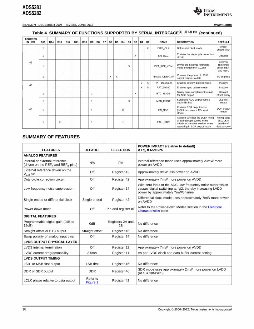
ADS5281ADS5282
SBAS397I ndashDECEMBER 2006ndashREVISED JUNE 2012 wwwticom
Table 4 SUMMARY OF FUNCTIONS SUPPORTED BY SERIAL INTERFACE(1) (2) (3) (4) (continued)ADDRESS
IN HEX D15 D14 D13 D12 D11 D10 D9 D8 D7 D6 D5 D4 D3 D2 D1 D0 NAME DESCRIPTION DEFAULT
Single-1 X DIFF_CLK Differential clock mode
ended clock
Enables the duty-cycle correction1 X EN_DCC Disabled
circuit
External42Drives the external reference reference
1 X EXT_REF_VCMmode through the VCM pin drives REFT
and REFB
Controls the phase of LCLK1 X X PHASE_DDRlt10gt 90 degrees
output relative to data
0 X PAT_DESKEW Enables deskew pattern mode Inactive45
X 0 PAT_SYNC Enables sync pattern mode Inactive
Binary twos complement format Straight1 1 X BTC_MODE
for ADC output offset binary
Serialized ADC output comes LSB-first1 1 X MSB_FIRST
out MSB-first output
Enables SDR output modeDDR output46 1 1 X EN_SDR (LCLK becomes a 12x input
modeclock)
Controls whether the LCLK rising Rising edgeor falling edge comes in the of LCLK in
1 X 1 1 FALL_SDRmiddle of the data window when middle ofoperating in SDR output mode data window
SUMMARY OF FEATURES
POWER IMPACT (relative to default)FEATURES DEFAULT SELECTION AT fS = 65MSPS
ANALOG FEATURES
Internal or external reference Internal reference mode uses approximately 23mW moreNA Pin(driven on the REFT and REFB pins) power on AVDD
External reference driven on the Off Register 42 Approximately 9mW less power on AVDDVCM pin
Duty cycle correction circuit Off Register 42 Approximately 7mW more power on AVDD
With zero input to the ADC low-frequency noise suppressionLow-frequency noise suppression Off Register 14 causes digital switching at fS2 thereby increasing LVDD
power by approximately 7mWchannel
Differential clock mode uses approximately 7mW more powerSingle-ended or differential clock Single-ended Register 42 on AVDD
Refer to the Power-Down Modes section in the ElectricalPower-down mode Off Pin and register 0F Characteristics table
DIGITAL FEATURES
Programmable digital gain (0dB to Registers 2A and0dB No difference12dB) 2B
Straight offset or BTC output Straight offset Register 46 No difference
Swap polarity of analog input pins Off Register 24 No difference
LVDS OUTPUT PHYSICAL LAYER
LVDS internal termination Off Register 12 Approximately 7mW more power on AVDD
LVDS current programmability 35mA Register 11 As per LVDS clock and data buffer current setting
LVDS OUTPUT TIMING
LSB- or MSB-first output LSB-first Register 46 No difference
SDR mode uses approximately 2mW more power on LVDDDDR or SDR output DDR Register 46 (at fS = 30MSPS)
Refer toLCLK phase relative to data output Register 42 No differenceFigure 1
18 Copyright copy 2006ndash2012 Texas Instruments Incorporated
ADS5281ADS5282
wwwticom SBAS397I ndashDECEMBER 2006ndashREVISED JUNE 2012
DESCRIPTION OF SERIAL REGISTERS
SOFTWARE RESET
ADDRESSIN HEX D15 D14 D13 D12 D11 D10 D9 D8 D7 D6 D5 D4 D3 D2 D1 D0 NAME
00 X RST
Software reset is applied when the RST bit is set to 1 setting this bit resets all internal registers and self-clearsto 0
POWER-DOWN MODES
ADDRESSIN HEX D15 D14 D13 D12 D11 D10 D9 D8 D7 D6 D5 D4 D3 D2 D1 D0 NAME
X X X X X X X X PDN_CHlt81gt
X PDN_PARTIAL0F
0 X PDN_COMPLETE
X 0 PDN_PIN_CFG
Each of the eight channels can be individually powered down PDN_CHltNgt controls the power-down mode forthe ADC channel ltNgt
In addition to channel-specific power-down the ADS528x also has two global power-down modesmdashpartialpower-down mode and complete power-down mode Partial power-down mode partially powers down the chiprecovery from this mode is much quicker provided that the clock has been running for at least 50μs beforeexiting this mode Complete power-down mode on the other hand completely powers down the chip andinvolves a much longer recovery time
In addition to programming the device for either of these two power-down modes (through either thePDN_PARTIAL or PDN_COMPLETE bits respectively) the PD pin itself can be configured as either a partialpower-down pin or a complete power-down pin control For example if PDN_PIN_CFG = 0 (default) when thePD pin is high the device enters complete power-down mode However if PDN_PIN_CFG = 1 when the PD pinis high the device enters partial power-down mode
LVDS DRIVE PROGRAMMABILITY
ADDRESSIN HEX D15 D14 D13 D12 D11 D10 D9 D8 D7 D6 D5 D4 D3 D2 D1 D0 NAME
X X X ILVDS_LCLKlt20gt
11 X X X ILVDS_FRAMElt20gt
X X X ILVDS_DATlt20gt
The LVDS drive strength of the bit clock (LCLKP or LCLKN) and the frame clock (ADCLKP or ADCLKN) can beindividually programmed The LVDS drive strengths of all the data outputs OUTP and OUTN can also beprogrammed to the same value
Copyright copy 2006ndash2012 Texas Instruments Incorporated 19
ADS5281ADS5282
SBAS397I ndashDECEMBER 2006ndashREVISED JUNE 2012 wwwticom
All three drive strengths (bit clock frame clock and data) are programmed using sets of three bits Table 5shows an example of how the drive strength of the bit clock is programmed (the method is similar for the frameclock and data drive strengths)
Table 5 Bit Clock Drive Strength (1)
ILVDS_LCLKlt2gt ILVDS_LCLKlt1gt ILVDS_LCLKlt0gt LVDS DRIVE STRENGTH FOR LCLKP AND LCLKN
0 0 0 35mA (default)
0 0 1 25mA
0 1 0 15mA
0 1 1 05mA
1 0 0 75mA
1 0 1 65mA
1 1 0 55mA
1 1 1 45mA
(1) Current settings lower than 15mA are not recommended
LVDS INTERNAL TERMINATION PROGRAMMABILITY
ADDRESSIN HEX D15 D14 D13 D12 D11 D10 D9 D8 D7 D6 D5 D4 D3 D2 D1 D0 NAME
X EN_LVDS_TERM
1 X X X TERM_LCLKlt20gt12
1 X X X TERM_FRAMElt20gt
1 X X X TERM_DATlt20gt
The LVDS buffers have high-impedance current sources driving the outputs When driving traces whosecharacteristic impedance is not perfectly matched with the termination impedance on the receiver side there maybe reflections back to the LVDS output pins of the ADS528x that cause degraded signal integrity By enabling aninternal termination (between the positive and negative outputs) for the LVDS buffers the signal integrity can besignificantly improved in such scenarios To set the internal termination mode the EN_LVDS_TERM bit shouldbe set to 1 Once this bit is set the internal termination values for the bit clock frame clock and data bufferscan be independently programmed using sets of three bits Table 6 shows an example of how the internaltermination of the LVDS buffer driving the bit clock is programmed (the method is similar for the frame clock anddata buffers) These termination values are only typical values and can vary by up to plusmn20 across temperatureand from device to device
Table 6 Bit Clock Internal Termination
INTERNAL TERMINATION BETWEENTERM_LCLKlt2gt TERM_LCLKlt1gt TERM_LCLKlt0gt LCLKP AND LCLKN IN Ω
0 0 0 None
0 0 1 260
0 1 0 150
0 1 1 94
1 0 0 125
1 0 1 80
1 1 0 66
1 1 1 55
20 Copyright copy 2006ndash2012 Texas Instruments Incorporated
ADS5281ADS5282
wwwticom SBAS397I ndashDECEMBER 2006ndashREVISED JUNE 2012
LOW-FREQUENCY NOISE SUPPRESSION MODE
ADDRESSIN HEX D15 D14 D13 D12 D11 D10 D9 D8 D7 D6 D5 D4 D3 D2 D1 D0 NAME
14 X X X X X X X X LFNS_CHlt81gt
The low-frequency noise suppression mode is specifically useful in applications where good noise performance isdesired in the frequency band of 0MHz to 1MHz (around dc) Setting this mode shifts the low-frequency noise ofthe ADS528x to approximately fS2 thereby moving the noise floor around dc to a much lower valueLFNS_CHlt81gt enables this mode individually for each channel
ANALOG INPUT INVERT
ADDRESSIN HEX D15 D14 D13 D12 D11 D10 D9 D8 D7 D6 D5 D4 D3 D2 D1 D0 NAME
24 X X X X X X X X INVERT_CHlt81gt
Normally the INP pin represents the positive analog input pin and INN represents the complementary negativeinput Setting the bits marked INVERT_CHlt81gt (individual control for each channel) causes the inputs to beswapped INN now represents the positive input and INP the negative input
LVDS TEST PATTERNS
ADDRESSIN HEX D15 D14 D13 D12 D11 D10 D9 D8 D7 D6 D5 D4 D3 D2 D1 D0 NAME
X 0 0 EN_RAMP
0 X 0 DUALCUSTOM_PAT
25 0 0 X SINGLE_CUSTOM_PAT
X X BITS_CUSTOM1lt1110gt
X X BITS_CUSTOM2lt1110gt
26 X X X X X X X X X X BITS_CUSTOM1lt90gt
27 X X X X X X X X X X BITS_CUSTOM2lt90gt
0 X PAT_DESKEW45
X 0 PAT_SYNC
The ADS528x can output a variety of test patterns on the LVDS outputs These test patterns replace the normalADC data output Setting EN_RAMP to 1 causes all the channels to output a repeating full-scale ramp patternThe ramp increments from zero code to full-scale code in steps of 1LSB every clock cycle After hitting the full-scale code it returns back to zero code and ramps again
The device can also be programmed to output a constant code by setting SINGLE_CUSTOM_PAT to 1 andprogramming the desired code in BITS_CUSTOM1lt110gt In this mode BITS_CUSTOM1lt110gt take the placeof the 12-bit ADC data at the output and are controlled by LSB-first and MSB-first modes in the same way asnormal ADC data are
The device may also be made to toggle between two consecutive codes by programming DUAL_CUSTOM_PATto 1 The two codes are represented by the contents of BITS_CUSTOM1lt110gt and BITS_CUSTOM2lt110gt
In addition to custom patterns the device may also be made to output two preset patterns1 Deskew patten Set using PAT_DESKEW this mode replaces the 12-bit ADC output Dlt110gt with the
010101010101 word2 Sync pattern Set using PAT_SYNC the normal ADC word is replaced by a fixed 111111000000 word
Note that only one of the above patterns should be active at any given instant
Copyright copy 2006ndash2012 Texas Instruments Incorporated 21
ADS5281ADS5282
SBAS397I ndashDECEMBER 2006ndashREVISED JUNE 2012 wwwticom
PROGRAMMABLE GAIN
ADDRESSIN HEX D15 D14 D13 D12 D11 D10 D9 D8 D7 D6 D5 D4 D3 D2 D1 D0 NAME
X X X X GAIN_CH1lt30gt
X X X X GAIN_CH2lt30gt2A
X X X X GAIN_CH3lt30gt
X X X X GAIN_CH4lt30gt
X X X X GAIN_CH5lt30gt
X X X X GAIN_CH6lt30gt2B
X X X X GAIN_CH7lt30gt
X X X X GAIN_CH8lt30gt
In applications where the full-scale swing of the analog input signal is much less than the 2VPP range supportedby the ADS528x a programmable gain can be set to achieve the full-scale output code even with a lower analoginput swing The programmable gain not only fills the output code range of the ADC but also enhances the SNRof the device by utilizing quantization information from some extra internal bits The programmable gain for eachchannel can be individually set using a set of four bits indicated as GAIN_CHNlt30gt for Channel N The gainsetting is coded in binary from 0dB to 12dB as shown in Table 7
Table 7 Gain Setting for Channel 1
GAIN_CH1lt3gt GAIN_CH1lt2gt GAIN_CH1lt1gt GAIN_CH1lt0gt CHANNEL 1 GAIN SETTING
0 0 0 0 0dB
0 0 0 1 1dB
0 0 1 0 2dB
0 0 1 1 3dB
0 1 0 0 4dB
0 1 0 1 5dB
0 1 1 0 6dB
0 1 1 1 7dB
1 0 0 0 8dB
1 0 0 1 9dB
1 0 1 0 10dB
1 0 1 1 11dB
1 1 0 0 12dB
1 1 0 1 Do not use
1 1 1 0 Do not use
1 1 1 1 Do not use
22 Copyright copy 2006ndash2012 Texas Instruments Incorporated
VREF = 15V -B
VCM
15V
VREF = 15V +T
VCM
15V
ADS5281ADS5282
wwwticom SBAS397I ndashDECEMBER 2006ndashREVISED JUNE 2012
CLOCK REFERENCE AND DATA OUTPUT MODES
ADDRESSIN HEX D15 D14 D13 D12 D11 D10 D9 D8 D7 D6 D5 D4 D3 D2 D1 D0 NAME
1 X DIFF_CLK
1 X EN_DCC42
1 X EXT_REF_VCM
1 X X PHASE_DDRlt10gt
1 1 X BTC_MODE
1 1 X MSB_FIRST46
1 1 X EN_SDR
1 X 1 1 FALL_SDR
INPUT CLOCK
The ADS528x is configured by default to operate with a single-ended input clockmdashCLKP is driven by a CMOSclock and CLKN is tied to 0 However by programming DIFF_CLK to 1 the device can be made to work with adifferential input clock on CLKP and CLKN Operating with a low-jitter differential clock usually gives better SNRperformance especially at input frequencies greater than 30MHz
In cases where the duty cycle of the input clock falls outside the 45 to 55 range it is recommended to enablean internal duty cycle correction circuit This enabling is done by setting the EN_DCC bit to 1
EXTERNAL REFERENCE
The ADS528x can be made to operate in external reference mode by pulling the INTEXT pin to 0 In this modethe REFT and REFB pins should be driven with voltage levels of 25V and 05V respectively and must haveenough drive strength to drive the switched capacitance loading of the reference voltages by each ADC Theadvantage of using the external reference mode is that multiple ADS528x units can be made to operate with thesame external reference thereby improving parameters such as gain matching across devices However inapplications that do not have an available high drive differential external reference the ADS528x can still bedriven with a single external reference voltage on the VCM pin When EXT_REF_VCM is set as 1 (and theINTEXT pin is set to 0) the VCM pin is configured as an input pin and the voltages on REFT and REFB aregenerated as shown in Equation 1 and Equation 2
(1)
(2)
Copyright copy 2006ndash2012 Texas Instruments Incorporated 23
PHASE_DDRlt10gt = 00
PHASE_DDRlt10gt = 01
PHASE_DDRlt10gt = 10
PHASE_DDRlt10gt = 11
ADCLKP
LCLKP
OUTP
ADCLKP
LCLKP
OUTP
ADCLKP
LCLKP
OUTP
ADCLKP
LCLKP
OUTP
ADCLKP
LCLKP
OUTP
ADS5281ADS5282
SBAS397I ndashDECEMBER 2006ndashREVISED JUNE 2012 wwwticom
BIT CLOCK PROGRAMMABILITY
The output interface of the ADS528x is normally a DDR interface with the LCLK rising edge and falling edgetransitions in the middle of alternate data windows This default phase is shown in Figure 1
Figure 1 Default Phase of LCLK
The phase of LCLK can be programmed relative to the output frame clock and data using bitsPHASE_DDRlt10gt The LCLK phase modes are shown in Figure 2
Figure 2 Phase Programmability Modes for LCLK
24 Copyright copy 2006ndash2012 Texas Instruments Incorporated
EN_SDR = 1 FALL_SDR = 0
EN_SDR = 1 FALL_SDR = 1
ADCLKP
LCLKP
OUTP
ADCLKP
LCLKP
OUTP
ADS5281ADS5282
wwwticom SBAS397I ndashDECEMBER 2006ndashREVISED JUNE 2012
In addition to programming the phase of LCLK in the DDR mode the device can also be made to operate in SDRmode by setting the EN_SDR bit to 1 In this mode the bit clock (LCLK) is output at 12x times the input clock ortwice the rate as in DDR mode Depending on the state of FALL_SDR LCLK may be output in either of the twomanners shown in Figure 3 As can be seen in Figure 3 only the LCLK rising (or falling) edge is used to capturethe output data in SDR mode
Figure 3 SDR Interface Modes
The SDR mode does not work well beyond 40MSPS because the LCLK frequency becomes very high
DATA OUTPUT FORMAT MODES
The ADC output by default is in straight offset binary mode Programming the BTC_MODE bit to 1 inverts theMSB and the output becomes binary twos complement mode
Also by default the first bit of the frame (following the rising edge of ADCLKP) is the LSB of the ADC outputProgramming the MSB_FIRST mode inverts the bit order in the word and the MSB is output as the first bitfollowing the ADCLKP rising edge
Copyright copy 2006ndash2012 Texas Instruments Incorporated 25
0
-
-
-
-
-
-
-
-
-
20
40
60
80
100
120
140
160
180
Input Frequency (MHz)
0 25
Am
plit
ude (
dB
)
2015105
SFDR = 884dBc
SNR = 709dBFS
SINAD = 708dBFS
THD = 875dBc
0
-
-
-
-
-
-
-
-
-
20
40
60
80
100
120
140
160
180
Input Frequency (MHz)
0 25
Am
plit
ude (
dB
)
2015105
SFDR = 856dBc
SNR = 705dBFS
SINAD = 704dBFS
THD = 839dBc
0
-
-
-
-
-
-
-
-
-
20
40
60
80
100
120
140
160
180
Input Frequency (MHz)
0 2 20
Am
plit
ude (
dB
)
1816141210864
SFDR = 853dBc
SNR = 708dBFS
SINAD = 707dBFS
THD = 893dBc
0
-
-
-
-
-
-
-
-
-
20
40
60
80
100
120
140
160
180
Input Frequency (MHz)
0 2 20
Am
plit
ude (
dB
)
1816141210864
SFDR = 828dBc
SNR = 702dBFS
SINAD = 70dBFS
THD = 823dBc
ADS5281ADS5282
SBAS397I ndashDECEMBER 2006ndashREVISED JUNE 2012 wwwticom
TYPICAL CHARACTERISTICSAt TA = +25degC AVDD = +33V LVDD = 18V clock frequency = 65MSPS differential clock mode 1VPP clock amplitude 50
clock duty cycle input frequency = 10MHz ndash1dBFS differential analog input 0dB digital gain setting 15V analog inputcommon-mode low-frequency noise suppression = off internal reference mode ISET resistor = 562kΩ and LVDS buffer
current setting = 35mA unless otherwise noted
SPECTRAL PERFORMANCE SPECTRAL PERFORMANCE(fS = 40MHz fIN = 10MHz) (fS = 40MHz fIN = 25MHz)
Figure 4 Figure 5
SPECTRAL PERFORMANCE SPECTRAL PERFORMANCE(fS = 50MHz fIN = 10MHz) (fS = 50MHz fIN = 25MHz)
Figure 6 Figure 7
26 Copyright copy 2006ndash2012 Texas Instruments Incorporated
0
-20
-40
-60
-80
-100
-120
-140
-180
Input Frequency (MHz)
0 33
Am
plit
ude (
dB
)
2015105
-160
SFDR = 862dBc
SNR = 705dBFS
SNR (0MHz to 1MHz) = 861dBFS
SINAD = 704dBFS
THD = 854dBc
25 30
92
87
82
77
72
67
Input Frequency (MHz)
5 30
Dynam
ic P
erf
orm
ance (
SN
R S
FD
R)
201510 25
SNR (dBFS)
SFDR (dBc)
f = 40MHzS
0
-
-
-
-
-
-
-
-
-
20
40
60
80
100
120
140
160
180
Input Frequency (MHz)
0 33
Am
plit
ude (
dB
)
2015105 25 30
SFDR = 909dBc
SNR = 708dBFS
SINAD = 707dBFS
THD = 904dBc
0
-20
-40
-60
-80
-100
-120
-140
-180
Input Frequency (MHz)
0 33
Am
plit
ude (
dB
)
2015105
-160
SFDR = 874dBc
SNR = 704dBFS
SNR (0MHz to 1MHz) = 819dBFS
SINAD = 703dBFS
THD = 864dBc
25 30
ADS5281ADS5282
wwwticom SBAS397I ndashDECEMBER 2006ndashREVISED JUNE 2012
TYPICAL CHARACTERISTICS (continued)At TA = +25degC AVDD = +33V LVDD = 18V clock frequency = 65MSPS differential clock mode 1VPP clock amplitude 50clock duty cycle input frequency = 10MHz ndash1dBFS differential analog input 0dB digital gain setting 15V analog inputcommon-mode low-frequency noise suppression = off internal reference mode ISET resistor = 562kΩ and LVDS buffercurrent setting = 35mA unless otherwise noted
SPECTRAL PERFORMANCE SPECTRAL PERFORMANCE(fS = 65MHz fIN = 10MHz) (fS = 65MHz fIN = 25MHz)
Figure 8 Figure 9
SPECTRAL PERFORMANCE LOW-FREQUENCY NOISESUPPRESSION MODE ENABLED
(fS = 65MHz fIN = 25MHz) DYNAMIC PERFORMANCE vs INPUT FREQUENCY
Figure 10 Figure 11
Copyright copy 2006ndash2012 Texas Instruments Incorporated 27
95
85
75
65
55
45
35
25
Input Amplitude (dBFS)
Dyn
am
ic P
erf
orm
an
ce
(S
NR
S
FD
R)
SNR (dBFS)
SFDR (dBc)
f = 65MHz
f = 10MHzS
IN
-60 0-50 -40 -30 -20 -10
94
89
84
79
74
69
Clock Amplitude (V Differential)PP
06 23
Dynam
ic P
erf
orm
ance (
SN
R S
FD
R)
1611
SNR (dBFS)
SFDR (dBc)
f = 65MHz
f = 10MHzS
IN
21
95
90
85
80
75
70
65
60
Digital Gain (dB)
0 12
Dyn
am
ic P
erf
orm
an
ce
(S
NR
S
FD
R)
642 8
SNR (dBFS)
SFDR (dBc)
f = 65MHz
f = 10MHzS
IN
10
95
90
85
80
75
70
65
60
AVDD (V)
30 36
Dynam
ic P
erf
orm
ance (
SN
R S
FD
R)
333231 34
SNR (dBFS)
SFDR (dBc)
f = 65MHz
f = 10MHzS
IN
35
92
87
82
77
72
67
Input Frequency (MHz)
5 30
Dynam
ic P
erf
orm
ance (
SN
R S
FD
R)
201510 25
SNR (dBFS)
SFDR (dBc)
f = 50MHzS
97
92
87
82
77
72
67
Input Frequency (MHz)
5 30
Dynam
ic P
erf
orm
ance (
SN
R S
FD
R)
201510 25
SNR (dBFS)
SFDR (dBc)
f = 65MHzS
ADS5281ADS5282
SBAS397I ndashDECEMBER 2006ndashREVISED JUNE 2012 wwwticom
TYPICAL CHARACTERISTICS (continued)At TA = +25degC AVDD = +33V LVDD = 18V clock frequency = 65MSPS differential clock mode 1VPP clock amplitude 50clock duty cycle input frequency = 10MHz ndash1dBFS differential analog input 0dB digital gain setting 15V analog inputcommon-mode low-frequency noise suppression = off internal reference mode ISET resistor = 562kΩ and LVDS buffercurrent setting = 35mA unless otherwise noted
DYNAMIC PERFORMANCE vs INPUT FREQUENCY DYNAMIC PERFORMANCE vs INPUT FREQUENCY
Figure 12 Figure 13
DYNAMIC PERFORMANCE vs DIGITAL GAIN DYNAMIC PERFORMANCE vs AVDD
Figure 14 Figure 15
DYNAMIC PERFORMANCE vs INPUT AMPLITUDE DYNAMIC PERFORMANCE vs CLOCK AMPLITUDE
Figure 16 Figure 17
28 Copyright copy 2006ndash2012 Texas Instruments Incorporated
94
89
84
79
74
69
External Reference Common-Mode Voltage (REF + REF )2 (V)T B
135 165
Dynam
ic P
erf
orm
ance (
SN
R S
FD
R)
150145140
SNR (dBFS)
SFDR (dBc)
f = 65MHz
f = 10MHzS
IN
155 160
External reference differential voltage maintained at 2V
94
89
84
79
74
69
Voltage on V (V)CM
135 165
Dynam
ic P
erf
orm
ance (
SN
R S
FD
R)
150145140
SNR (dBFS)
SFDR (dBc)
f = 65MHz
f = 10MHzS
IN
155 160
94
89
84
79
74
69
Analog Input Common-Mode Voltage (V)
130 170
Dynam
ic P
erf
orm
ance (
SN
R S
FD
R)
140135
SNR (dBFS)
SFDR (dBc)
f = 65MHz
f = 10MHzS
IN
145 165160155150
94
89
84
79
74
69
External Reference Differential Voltage REF REF (V)-T B
16 24
Dynam
ic P
erf
orm
ance (
SN
R S
FD
R)
191817
SNR (dBFS)
SFDR (dBc)
f = 65MHz
f = 10MHzS
IN
20 232221
External reference common-mode voltage
maintained at 15V
ADS5281ADS5282
wwwticom SBAS397I ndashDECEMBER 2006ndashREVISED JUNE 2012
TYPICAL CHARACTERISTICS (continued)At TA = +25degC AVDD = +33V LVDD = 18V clock frequency = 65MSPS differential clock mode 1VPP clock amplitude 50clock duty cycle input frequency = 10MHz ndash1dBFS differential analog input 0dB digital gain setting 15V analog inputcommon-mode low-frequency noise suppression = off internal reference mode ISET resistor = 562kΩ and LVDS buffercurrent setting = 35mA unless otherwise noted
DYNAMIC PERFORMANCE vs ANALOG INPUT COMMON- DYNAMIC PERFORMANCE vs EXTERNAL REFERENCEMODE VOLTAGE DIFFERENTIAL VOLTAGE
Figure 18 Figure 19
DYNAMIC PERFORMANCE vs EXTERNAL REFERENCE DYNAMIC PERFORMANCE vs EXTERNAL REFERENCECOMMON-MODE VOLTAGE FORCED THROUGH VCM
Figure 20 Figure 21
Copyright copy 2006ndash2012 Texas Instruments Incorporated 29
05
04
03
02
01
0
-01
-02
-05
Code (LSB)
0 4096
INL
(L
SB
)
30722048 25601536 35841024512
-04
-03
f = 50MSPS
f = 5MHzS
IN
035
025
015
005
-005
-015
-035
Code (LSB)
0 4096
DN
L (
LS
B)
30722048 25601536 35841024512
-025
f = 50MSPS
f = 5MHzS
IN
60
50
40
30
20
10
0
Code Bin (LSB)
2049
Occurr
ence (
)
20532051 2054
f = 65MSPSS
2050 2052
0 0037 028
5192
4743
10
-10
-30
-50
-70
-90
-110
-130
-150
Input Frequency (MHz)
0 2 20
Am
plit
ude (
dB
)
1816141210864
f = 65MHz
f = 10MHz ( 7dBFS)
f = 161MHz ( 7dBFS)
IMD = 97dBFS
-
-
-
S
1
2
95
90
85
80
75
70
65
60
Clock Duty Cycle ()
35 65
Dynam
ic P
erf
orm
ance (
SN
R S
FD
R)
504540 55
SNR (dBFS)
SFDR (dBc)
f = 65MHz
f = 10MHzS
IN
60
95
85
80
75
70
60
Clock Duty Cycle ()
20 80
Dynam
ic P
erf
orm
ance (
SN
R S
FD
R)
504030 60
SNR (dBFS)
SFDR (dBc)
f = 65MHz
f = 10MHzS
IN
90
70
65
ADS5281ADS5282
SBAS397I ndashDECEMBER 2006ndashREVISED JUNE 2012 wwwticom
TYPICAL CHARACTERISTICS (continued)At TA = +25degC AVDD = +33V LVDD = 18V clock frequency = 65MSPS differential clock mode 1VPP clock amplitude 50clock duty cycle input frequency = 10MHz ndash1dBFS differential analog input 0dB digital gain setting 15V analog inputcommon-mode low-frequency noise suppression = off internal reference mode ISET resistor = 562kΩ and LVDS buffercurrent setting = 35mA unless otherwise noted
DYNAMIC PERFORMANCE vs CLOCK DUTY CYCLE DCC DYNAMIC PERFORMANCE vs CLOCK DUTY CYCLE DCCDISABLED ENABLED
Figure 22 Figure 23
HISTOGRAM OF OUTPUT CODE FOR ZERO INPUT INTERMODULATION DISTORTION
Figure 24 Figure 25
INTEGRAL NONLINEARITY DIFFERENTIAL NONLINEARITY
Figure 26 Figure 27
30 Copyright copy 2006ndash2012 Texas Instruments Incorporated
064
062
060
058
056
054
052
Sta
ndard
Devia
tion (
LS
B)
0 1 2 3 4 5 6
Overload Signal Amplitude (dBFS)
f = 65MSPS
f = 5MHzS
IN
Standard Deviation of
2nd Point After Overload
Standard Deviation of
1st Point After Overload
tS
16384 t (Group 1)S
Set 1 Point 1 (of 16) Set 1 Point 2 (of 16)
First point after overload (Set 1)
First point after overload (Set 2)
Second point after overload (Set 2)
Second point after overload (Set 1)
Overload
Amplitude
NOTES
Input sine wave phase is repetitive over 16384 clock cycles
16 such repetitive groups (of 16384 clock cycles) are capturedndasha total of 262144 points
Standard deviation of every set of are analyzed over the 16 groups
Worst case of all such standard deviations are plotted in the graphs
first and second points after overload
+FS
-FS
070
068
066
064
062
060
058
056
054
052
050
Sta
nd
ard
De
via
tio
n (
in L
SB
)
0 1 2 3 4 5 6
Overload Signal Amplitude (dBFS)
f = 50MSPS
f = 5MHzS
IN Standard Deviation of
2nd Point After Overload
Standard Deviation of
1st Point After Overload
170
130
110
90
70
30
Clock Frequency (MSPS)
5 75
I I
(mA
)A
VD
DLV
DD
352515 45
ILVDD
IAVDD
Zero Input on All Channels
Internal Reference Mode150
55
50
65
075
055
035
015
-005
-025
-065
Code (LSB)
0 4096
INL
(LS
B)
30722048 25601536 35841024512
-045
f = 65MSPS
f = 5MHzS
IN
035
025
015
005
-005
-015
-035
Code (LSB)
0 4096
DN
L (
LS
B)
30722048 25601536 35841024512
-025
f = 65MSPS f = 5MHzS IN
ADS5281ADS5282
wwwticom SBAS397I ndashDECEMBER 2006ndashREVISED JUNE 2012
TYPICAL CHARACTERISTICS (continued)At TA = +25degC AVDD = +33V LVDD = 18V clock frequency = 65MSPS differential clock mode 1VPP clock amplitude 50clock duty cycle input frequency = 10MHz ndash1dBFS differential analog input 0dB digital gain setting 15V analog inputcommon-mode low-frequency noise suppression = off internal reference mode ISET resistor = 562kΩ and LVDS buffercurrent setting = 35mA unless otherwise noted
INTEGRAL NONLINEARITY DIFFERENTIAL NONLINEARITY
Figure 28 Figure 29
AVDD AND LVDD POWER-SUPPLY CURRENTSvs CLOCK FREQUENCY OVERLOAD RECOVERY AT 50MSPS
Figure 30 Figure 31
OVERLOAD RECOVERY AT 65MSPS
Figure 32 Figure 33 Overload Recovery
Copyright copy 2006ndash2012 Texas Instruments Incorporated 31
ADS5281ADS5282
SBAS397I ndashDECEMBER 2006ndashREVISED JUNE 2012 wwwticom
APPLICATION INFORMATION
The ADC output goes to a serializer that operatesTHEORY OF OPERATION from a 12x clock generated by the PLL The 12 databits from each channel are serialized and sent LSBThe ADS528x devices are a family of 8-channelfirst In addition to serializing the data the serializerhigh-speed CMOS ADCs The 12 bits given out byalso generates a 1x clock and a 6x clock Theseeach channel are serialized and sent out on a singleclocks are generated in the same way the serializedpair of pins in LVDS format All eight channels of thedata are generated so these clocks maintain perfectADS528x operate from a single clock (ADCLK) Thesynchronization with the data The data and clocksampling clocks for each of the eight channels areoutputs of the serializer are buffered externally usinggenerated from the input clock using a carefullyLVDS buffers Using LVDS buffers to transmit datamatched clock buffer tree The 12x clock required forexternally has multiple advantages such as athe serializer is generated internally from ADCLKreduced number of output pins (saving routing spaceusing a phase-locked loop (PLL) A 6x and a 1x clockon the board) reduced power consumption andare also output in LVDS format along with the datareduced effects of digital noise coupling to the analogto enable easy data capture The ADS528x operatescircuit inside the ADS528xfrom internally-generated reference voltages that are
trimmed to improve to a high level of accuracy The ADS528x operates from two sets of supplies andTrimmed references improve the gain matching grounds The analog supply and ground set isacross devices and provide the option to operate the identified as AVDD and AVSS while the digital set isdevices without having to externally drive and route identified by LVDD and LVSSreference lines The nominal values of REFT andREFB are 25V and 05V respectively The ANALOG INPUTreferences are internally scaled down differentially bya factor of 2 This scaling results in a differential input The analog input consists of a switched-capacitorof ndash1V to correspond to the zero code of the ADC based differential sample-and-hold architecture Thisand a differential input of +1V to correspond to the differential topology results in very good acfull-scale code (4095 LSB) VCM (the common-mode performance even for high input frequencies at highvoltage of REFT and REFB) is also made available sampling rates The INN and INP pins must beexternally through a pin and is nominally 15V externally biased around a common-mode voltage of
15V available on VCM For a full-scale differentialThe ADC employs a pipelined converter architectureinput each input pin (INN and INP) must swingthat consists of a combination of multi-bit and single-symmetrically between VCM + 05V and VCM ndash 05Vbit internal stages Each stage feeds its data into theresulting in a 2VPP differential input swing Thedigital error correction logic ensuring excellentmaximum input peak-to-peak differential swing isdifferential linearity and no missing codes at the 12-determined to be the difference between the internalbit levelreference voltages REFT (25V nominal) and REFB(05V nominal) Figure 34 illustrates the model of theinput driving circuit
32 Copyright copy 2006ndash2012 Texas Instruments Incorporated
CM Buffer
Internal
Voltage
Reference
Input
Circuitry
INP
INN
VCM
12kW
12kW
ADS528x
(2mA) facute S
50MSPS
5nH to 9nH (TQFP-80)
2nH to 3nH (QFN-64)
15pF
to 24pF
IN OUT
INP
15pF to
25pF
1W
1000W
to 1440W
5W
to 10W
1000W
to 1440W
5nH to 9nH (TQFP-80)
2nH to 3nH (QFN-64)
INN
15pF to
25pF
1W
15W
to 25W
15W
to 30W
02pF
to 03pF
IN OUT
15pF
to 24pF
IN OUT
5W
to 10W
15W
to 25W
15W
to 30W
IN OUT
IN
OUT
16 to 32W W
IN OUT
IN OUT
OUTP
OUTN
Switches that are ON
in SAMPLE phase
Switches that are ON
in HOLD phase
ADS5281ADS5282
wwwticom SBAS397I ndashDECEMBER 2006ndashREVISED JUNE 2012
Figure 34 Analog Input Circuit Model
during ac-coupling by increasing VCM by roughlyInput Common-Mode Current 75mV When operating above 50MSPS it is
recommended that additional parallel resistors beThe input stage of all eight ADCs together sinks aadded externally to restore the input common-modecommon-mode current on the order of 2mA atto at least 14V if the inputs are to be ac-coupled50MSPS Equation 3 describes the dependency of
the common-mode current and the samplingfrequency
(3)
If the driving stage is dc-coupled to the inputs thenEquation 3 can be used to determine its common-mode drive capability and impedance The inputs canalso be ac-coupled to the INN and INP pins In thatcase the input common-mode is set by two internal12kΩ resistors connecting the input pins to VCM Thisarchitecture is shown in Figure 35
When the inputs are ac-coupled there is a drop inthe voltages at INP and INN relative to VCM This can Dashed area denotes one of eight channelsbe computed from Equation 3 At 50MSPS for
Figure 35 Common-Mode Biasing of Input Pinsexample the drop at each of the 16 input pins is150mV which is not optimal for ADC operationInitialization Registers 1 and 5 described in theInitialization Registers table can be used to partiallyreduce the effect of this input common-mode drop
Copyright copy 2006ndash2012 Texas Instruments Incorporated 33
01 Fm 50W
50W
200W
200W
INP
VCM
INN
01 Fm
12 21
47W
47W
01 Fm
01 Fm
25W
25W
11
INP
VCM
INN
ADS5281ADS5282
SBAS397I ndashDECEMBER 2006ndashREVISED JUNE 2012 wwwticom
Driving Circuit At high input frequencies the mismatch in thetransformer parasitic capacitance (between theFor optimum performance the analog inputs must bewindings) results in degraded even-order harmonicdriven differentially This approach improves theperformance Connecting two identical RFcommon-mode noise immunity and even-ordertransformers back-to-back helps to minimize thisharmonic rejection Input configurations using RFmismatch and good performance is obtained fortransformers suitable for low and high inputhigh-frequency input signals An additionalfrequencies are shown in Figure 36 and Figure 37termination resistor pair is required between the tworespectively The single-ended signal is fed to thetransformers as shown in Figure 37 The center pointprimary winding of the RF transformer Theof this termination is connected to ground to improvetransformer is terminated by 50Ω resistor on thethe balance between the positive and negative sidessecondary side Placing the termination on theThe values of the terminations between thesecondary side helps to shield the kicks caused bytransformers and on the secondary side must bethe input sampling capacitors from the RFchosen to achieve an overall 50Ω (in the case of 50Ωtransformer leakage inductances The termination issource impedance)accomplished by two 25Ω resistors connected in
series with the center point connected to the 15Vcommon-mode The 47Ω resistor in series with eachinput pin is required to damp the ringing caused bythe device package parasitics
Figure 36 Drive Circuit at Low Input Frequencies
Figure 37 Drive Circuit at High Input Frequencies
34 Copyright copy 2006ndash2012 Texas Instruments Incorporated
CLKP
CLKN
CMOS Clock Input
01 Fm
01 Fm
CLKP
CLKN
CMOS Single-Ended
Clock
0V
CLKP
CLKN
Differential Sine-Wave
PECL or LVDS Clock Input
01 Fm
01 Fm
5kW 5kW
VCM
CLKP
CLKN
VCM
ADS5281ADS5282
wwwticom SBAS397I ndashDECEMBER 2006ndashREVISED JUNE 2012
CLOCK INPUT
The eight channels on the device operate from asingle ADCLK input To ensure that the aperturedelay and jitter are the same for all channels a clocktree network is used to generate individual samplingclocks to each channel The clock paths for all thechannels are matched from the source point to thesampling circuit This architecture ensures that theperformance and timing for all channels are identicalThe use of the clock tree for matching introduces anaperture delay that is defined as the delay betweenthe rising edge of ADCLK and the actual instant ofsampling The aperture delays for all the channelsare matched to the best possible extent A mismatchof plusmn20ps (plusmn3σ) could exist between the apertureinstants of the eight ADCs within the same chip Figure 39 Internal Clock BufferHowever the aperture delays of ADCs across twodifferent chips can be several hundred picosecondsapart
The ADS528x can be made to operate either inCMOS single-ended clock mode (default isDIFF_CLK = 0) or differential clock mode (SINELVPECL or LVDS) When operating in the single-ended clock mode CLKN must be forced to 0VDCand the single-ended CMOS applied on the CLKP pinThis operation is shown in Figure 38
Figure 40 Differential Clock Driving Circuit(DIFF_CLK = 1)
Figure 38 Single-Ended Clock Driving Circuit(DIFF_CLK = 0)
When configured to operate in the differential clock Figure 41 Single-Ended Clock Driving Circuitmode (register bit DIFF_CLK = 1) the ADS528x clock When DIFF_CLK = 1inputs can be driven differentially (SINE LVPECL orLVDS) with little or no difference in performance
For best performance the clock inputs must bebetween them or with a single-ended (LVCMOS)driven differentially in order to reduce susceptibility toThe common-mode voltage of the clock inputs is setcommon-mode noise For high input frequencyto VCM using internal 5kΩ resistors as shown insampling it is recommended to use a clock sourceFigure 39 This method allows using transformer-with very low jitter Bandpass filtering of the clockcoupled drive circuits for a sine wave clock or ac-source can help reduce the effect of jitter If the dutycoupling for LVPECL and LVDS clock sources ascycle deviates from 50 by more than 2 or 3 it isshown in Figure 40 When operating in the differentialrecommended to enable the DCC through register bitclock mode the single-ended CMOS clock can be ac-EN_DCCcoupled to the CLKP input with CLKN (pin 11)
connected to ground with a 01μF capacitor asshown in Figure 41
Copyright copy 2006ndash2012 Texas Instruments Incorporated 35
Threshold 1 Threshold 2 Threshold 3
10 MHz 45 MHz 65 MHz
Sampling Frequency
ADS5281ADS5282
SBAS397I ndashDECEMBER 2006ndashREVISED JUNE 2012 wwwticom
PLL OPERATION ACROSS SAMPLING Step 2 Disable the PLL automatic switch and setFREQUENCY the PLL configuration depending on the clock
frequencyThe ADS528X uses a PLL for generating the highspeed bit clock (LCLK) the frame clock (ADCLK) amp SAMPLE CLOCK FREQUENCY REGISTER SETTING (Hex)internal clocks for the serializer operation RANGE (MSPS)
Min Max Address DataTo enable operation across the entire frequencyrange the PLL is automatically configured to one of 10 25 E3 0060four states depending on the sampling clock 15 45 E3 00A0frequency range The frequency range detection isautomatic and each time the sampling frequency With the above settings applied for the respectivecrosses a threshold the PLL changes its frequency ranges the part will continue toconfiguration to a new state To prevent unwanted operate as per the stated datasheet specificationstoggling of PLL state around a threshold the circuit for all timing parameters at all specifiedhas an inbuilt hysteresis The ADS528x has three frequencies EXCEPT for the timing specificationsthresholds ndash taking into account the hysteresis range at 40MSPS At 40MSPS the affected parametersof each threshold variation across devices and are ndash Data setup time Data hold time and Clocktemperature the thresholds can span the sampling propagation delay (refer to LVDS Timing )clock frequency range from 10MHz to 45MHz 2 For sampling clock frequency ge 45MSPS
As there are no PLL thresholds beyond 45MHzno change in PLL configuration can occur as thetemperature in the system stabilizes TheADS528x can be used in the system withoutusing the above software fix
INPUT OVER-VOLTAGE RECOVERY
The differential peak-to-peak full-scale rangesupported by the ADS528x is nominally 20V TheADS528x is specially designed to handle an over-
Figure 42 Variation of Thresholds Across voltage condition where the differential peak-to-peakSampling Frequency voltage can be up to twice the ADC full-scale range
If the input common-mode is not considerably offfrom VCM during overload (less than 300mV aroundBased on actual system clock frequency there arethe nominal value of 15V) recovery from an over-two scenariosvoltage pulse input of twice the amplitude of a full-1 For sampling clock frequency lt 45MSPSscale pulse is expected to be within one clock cycle
After system power up depending on the when the input switches from overload to zero signalfrequency of operation and the frequencythreshold for the given device the frequency REFERENCE CIRCUITrange detection circuit may change state once In
The digital beam-forming algorithm in an ultrasoundsome applications where a timing calibrationsystem relies on gain matching across all receivermight be done at the system level once afterchannels A typical system would have about 12 octalpower up this subsequent change of the PLLADCs on the board In such a case it is critical tostate might be undesirable as it can cause a lossensure that the gain is matched essentially requiringof alignment in the received data A software fixthe reference voltages seen by all the ADCs to be thefor eliminating this one-time change of PLL statesame Matching references within the eight channelsexists using the serial register interfaceof a chip is done by using a single internal referencendash Disable the automatic switch of the PLLvoltage buffer Trimming the reference voltages onconfiguration based on frequency detectedeach chip during production ensures that thendash In addition to disabling the switching it is alsoreference voltages are well-matched across differentrequired to set the PLL to the correctchipsconfiguration depending on the sample clock
frequency used in the system All bias currents required for the internal operation ofthe device are set using an external resistor toThe following sequence of register writes must beground at the ISET pin Using a 562kΩ resistor on ISETfollowedgenerates an internal reference current of 20μA This
Step 1 Write Address = 0x01 Data = 0x0010 current is mirrored internally to generate the biascurrent for the internal blocks Using a larger external
36 Copyright copy 2006ndash2012 Texas Instruments Incorporated
VREF = 15V -B
VCM
15V
VREF = 15V +T
VCM
15V
REFT
REFB
ISET
01 Fm 22 Fm
0 to
2
W
W
0 toW
2W
562kW
22 Fm 01 Fm
ADS528x
ADS5281ADS5282
wwwticom SBAS397I ndashDECEMBER 2006ndashREVISED JUNE 2012
resistor at ISET reduces the reference bias current and The device also supports the use of externalthereby scales down the device operating power reference voltages There are two methods to forceHowever it is recommended that the external resistor the references externally The first method involvesbe within 10 of the specified value of 562kΩ so pulling INTEXT low and forcing externally REFT andthat the internal bias margins for the various blocks REFB to 25V and 05V nominally respectively In thisare proper mode the internal reference buffer goes to a 3-state
output The external reference driving circuit shouldBuffering the internal bandgap voltage also generates be designed to provide the required switching currentthe common-mode voltage VCM which is set to the for the eight ADCs inside the chip It should be notedmidlevel of REFT and REFB and is accessible on a that in this mode VCM and ISET continue to bepin (pin 65 in TQFP-80 package pin 53 in QFN-64 generated from the internal bandgap voltage as inpackage) It is meant as a reference voltage to derive the internal reference mode It is therefore importantthe input common-mode if the input is directly to ensure that the common-mode voltage of thecoupled It can also be used to derive the reference externally-forced reference voltages matches tocommon-mode voltage in the external reference within 50mV of VCMmode The suggested decoupling for the referencepins is shown in Figure 43 The second method of forcing the reference voltages
externally can be accessed by pulling INTEXT lowand programming the serial interface to drive theexternal reference mode through the VCM pin (registerbit called EXT_REF_VCM) In this mode VCMbecomes configured as an input pin that can bedriven from external circuitry The internal referencebuffers driving REFT and REFB are active in thismode Forcing 15V on the VCM pin in the moderesults in REFT and REFB coming to 25V and 05Vrespectively In general the voltages on REFT andREFB in this mode are given by Equation 4 andEquation 5 respectively
(4)Figure 43 Suggested Decoupling on the
Reference Pins(5)
The state of the reference voltage internal buffersduring various combinations of the PD INTEXT andEXT_REF_VCM register bits is described in Table 8
Table 8 State of Reference Voltages for Various Combinations of PD INTEXT and EXT_REF_VCM
REGISTER BIT INTERNAL BUFFER STATE
PD 0 0 1 1 0 0 1 1
INTEXT 0 1 0 1 0 1 0 1
EXT_REF_VCM 0 0 0 0 1 1 1 1
REFT buffer 3-state 25V 3-state 25V (1) 15V + VCM15V Do not use 25V (1) Do not use
REFB buffer 3-state 05V 3-state 05V (1) 15V ndash VCM15V Do not use 05V (1) Do not use
VCM pin 15V 15V 15V 15V Force Do not use Force Do not use
(1) Weakly forced with reduced strengthsections while LVDD and LVSS are used to denotethe digital supplies Care is taken to ensure that thereNOISE COUPLING ISSUESis minimal interaction between the supply sets within
High-speed mixed signals are sensitive to various the device The extent of noise coupled andtypes of noise coupling One primary source of noise transmitted from the digital to the analog sectionsis the switching noise from the serializer and the depends onoutput buffers Maximum care is taken to isolate
1 The effective inductances of each of the supplythese noise sources from the sensitive analog blocksand ground setsAs a starting point the analog and digital domains of
2 The isolation between the digital and analogthe device are clearly demarcated AVDD and AVSSsupply and ground setsare used to denote the supplies for the analog
Copyright copy 2006ndash2012 Texas Instruments Incorporated 37
ADS5281ADS5282
SBAS397I ndashDECEMBER 2006ndashREVISED JUNE 2012 wwwticom
Smaller effective inductance of the supply and ground It is recommended that the isolation be maintained onpins leads to better noise suppression For this the board by using separate supplies to drive AVDDreason multiple pins are used to drive each supply and LVDD as well as separate ground planes forand ground It is also critical to ensure that the AVSS and LVSS The use of LVDS buffers reducesimpedances of the supply and ground lines on the the injected noise considerably compared to CMOSboard are kept to the minimum possible values Use buffers The current in the LVDS buffer isof ground planes in the printed circuit board (PCB) as independent of the direction of switching Also thewell as large decoupling capacitors between the low output swing as well as the differential nature ofsupply and ground lines are necessary to obtain the the LVDS buffer results in low-noise couplingbest possible SNR performance from the device
38 Copyright copy 2006ndash2012 Texas Instruments Incorporated
ADS5281ADS5282
wwwticom SBAS397I ndashDECEMBER 2006ndashREVISED JUNE 2012
REVISION HISTORY
Changes from Revision G (March 2008) to Revision H Page
bull Changed second table and conditions in the Initialization Registers section 3
bull Changed In Input Common-Mode Current section changed initialization register 5 to initialization registers 1 and 5to reflect change in Initialization Registers table 33
Changes from Revision F (March 2008) to Revision G Page
bull Deleted note (3) of Ordering Information table to indicate device status is now Production Data for all parts 2
bull Added new note (3) of Ordering Information table to indicate the quantity of transport media is available in thePackage Option Addendum 2
bull Added note (1) to Initialization Registers section to indicate it is no longer necessary to program initializationregisters 1 to 4 3
bull Changed maximum specifications for ADS5282 column in the Power SupplymdashInternal Reference Mode section ofElectrical Characteristics (By Device) table 6
bull Changed minimum specification for ADS5282 column in the f = 10 MHz row of the SNR section of ElectricalCharacteristics (By Device) table 6
Changes from Revision H (March 2008) to Revision I Page
bull Added table in the INITIALIZATION REGISTERS section 3
bull Added table in the LVDS OUTPUT TIMING CHARACTERISTICS section 14
bull Added PLL OPERATION ACROSS SAMPLING FREQUENCY section 36
Copyright copy 2006ndash2012 Texas Instruments Incorporated 39
PACKAGE OPTION ADDENDUM
wwwticom 26-Oct-2016
Addendum-Page 1
PACKAGING INFORMATION
Orderable Device Status(1)
Package Type PackageDrawing
Pins PackageQty
Eco Plan(2)
LeadBall Finish(6)
MSL Peak Temp(3)
Op Temp (degC) Device Marking(45)
Samples
ADS5281IPFP ACTIVE HTQFP PFP 80 96 Green (RoHSamp no SbBr)
CU NIPDAU Level-3-260C-168 HR -40 to 85 ADS5281I
ADS5281IPFPR ACTIVE HTQFP PFP 80 1000 Green (RoHSamp no SbBr)
CU NIPDAU Level-3-260C-168 HR -40 to 85 ADS5281I
ADS5281IRGCR ACTIVE VQFN RGC 64 2000 Green (RoHSamp no SbBr)
CU NIPDAU Level-3-260C-168 HR -40 to 85 AZ5281
ADS5281IRGCT ACTIVE VQFN RGC 64 250 Green (RoHSamp no SbBr)
CU NIPDAU Level-3-260C-168 HR -40 to 85 AZ5281
ADS5282IRGCR ACTIVE VQFN RGC 64 2000 Green (RoHSamp no SbBr)
CU NIPDAU Level-3-260C-168 HR -40 to 85 AZ5282
ADS5282IRGCT ACTIVE VQFN RGC 64 250 Green (RoHSamp no SbBr)
CU NIPDAU Level-3-260C-168 HR -40 to 85 AZ5282
(1) The marketing status values are defined as followsACTIVE Product device recommended for new designsLIFEBUY TI has announced that the device will be discontinued and a lifetime-buy period is in effectNRND Not recommended for new designs Device is in production to support existing customers but TI does not recommend using this part in a new designPREVIEW Device has been announced but is not in production Samples may or may not be availableOBSOLETE TI has discontinued the production of the device
(2) Eco Plan - The planned eco-friendly classification Pb-Free (RoHS) Pb-Free (RoHS Exempt) or Green (RoHS amp no SbBr) - please check httpwwwticomproductcontent for the latest availabilityinformation and additional product content detailsTBD The Pb-FreeGreen conversion plan has not been definedPb-Free (RoHS) TIs terms Lead-Free or Pb-Free mean semiconductor products that are compatible with the current RoHS requirements for all 6 substances including the requirement thatlead not exceed 01 by weight in homogeneous materials Where designed to be soldered at high temperatures TI Pb-Free products are suitable for use in specified lead-free processesPb-Free (RoHS Exempt) This component has a RoHS exemption for either 1) lead-based flip-chip solder bumps used between the die and package or 2) lead-based die adhesive used betweenthe die and leadframe The component is otherwise considered Pb-Free (RoHS compatible) as defined aboveGreen (RoHS amp no SbBr) TI defines Green to mean Pb-Free (RoHS compatible) and free of Bromine (Br) and Antimony (Sb) based flame retardants (Br or Sb do not exceed 01 by weightin homogeneous material)
(3) MSL Peak Temp - The Moisture Sensitivity Level rating according to the JEDEC industry standard classifications and peak solder temperature
(4) There may be additional marking which relates to the logo the lot trace code information or the environmental category on the device
(5) Multiple Device Markings will be inside parentheses Only one Device Marking contained in parentheses and separated by a ~ will appear on a device If a line is indented then it is a continuationof the previous line and the two combined represent the entire Device Marking for that device
PACKAGE OPTION ADDENDUM
wwwticom 26-Oct-2016
Addendum-Page 2
(6) LeadBall Finish - Orderable Devices may have multiple material finish options Finish options are separated by a vertical ruled line LeadBall Finish values may wrap to two lines if the finishvalue exceeds the maximum column width
Important Information and DisclaimerThe information provided on this page represents TIs knowledge and belief as of the date that it is provided TI bases its knowledge and belief on informationprovided by third parties and makes no representation or warranty as to the accuracy of such information Efforts are underway to better integrate information from third parties TI has taken andcontinues to take reasonable steps to provide representative and accurate information but may not have conducted destructive testing or chemical analysis on incoming materials and chemicalsTI and TI suppliers consider certain information to be proprietary and thus CAS numbers and other limited information may not be available for release
In no event shall TIs liability arising out of such information exceed the total purchase price of the TI part(s) at issue in this document sold by TI to Customer on an annual basis
TAPE AND REEL INFORMATION
All dimensions are nominal
Device PackageType
PackageDrawing
Pins SPQ ReelDiameter
(mm)
ReelWidth
W1 (mm)
A0(mm)
B0(mm)
K0(mm)
P1(mm)
W(mm)
Pin1Quadrant
ADS5281IPFPR HTQFP PFP 80 1000 3300 244 150 150 15 200 240 Q2
ADS5281IRGCR VQFN RGC 64 2000 3300 164 93 93 15 120 160 Q2
ADS5281IRGCT VQFN RGC 64 250 1800 164 93 93 15 120 160 Q2
ADS5282IRGCR VQFN RGC 64 2000 3300 164 93 93 15 120 160 Q2
ADS5282IRGCT VQFN RGC 64 250 1800 164 93 93 15 120 160 Q2
PACKAGE MATERIALS INFORMATION
wwwticom 14-May-2015
Pack Materials-Page 1
All dimensions are nominal
Device Package Type Package Drawing Pins SPQ Length (mm) Width (mm) Height (mm)
ADS5281IPFPR HTQFP PFP 80 1000 3670 3670 450
ADS5281IRGCR VQFN RGC 64 2000 3366 3366 286
ADS5281IRGCT VQFN RGC 64 250 2130 1910 550
ADS5282IRGCR VQFN RGC 64 2000 3366 3366 286
ADS5282IRGCT VQFN RGC 64 250 2130 1910 550
PACKAGE MATERIALS INFORMATION
wwwticom 14-May-2015
Pack Materials-Page 2
wwwticom
IMPORTANT NOTICE
Texas Instruments Incorporated and its subsidiaries (TI) reserve the right to make corrections enhancements improvements and otherchanges to its semiconductor products and services per JESD46 latest issue and to discontinue any product or service per JESD48 latestissue Buyers should obtain the latest relevant information before placing orders and should verify that such information is current andcomplete All semiconductor products (also referred to herein as ldquocomponentsrdquo) are sold subject to TIrsquos terms and conditions of salesupplied at the time of order acknowledgmentTI warrants performance of its components to the specifications applicable at the time of sale in accordance with the warranty in TIrsquos termsand conditions of sale of semiconductor products Testing and other quality control techniques are used to the extent TI deems necessaryto support this warranty Except where mandated by applicable law testing of all parameters of each component is not necessarilyperformedTI assumes no liability for applications assistance or the design of Buyersrsquo products Buyers are responsible for their products andapplications using TI components To minimize the risks associated with Buyersrsquo products and applications Buyers should provideadequate design and operating safeguardsTI does not warrant or represent that any license either express or implied is granted under any patent right copyright mask work right orother intellectual property right relating to any combination machine or process in which TI components or services are used Informationpublished by TI regarding third-party products or services does not constitute a license to use such products or services or a warranty orendorsement thereof Use of such information may require a license from a third party under the patents or other intellectual property of thethird party or a license from TI under the patents or other intellectual property of TIReproduction of significant portions of TI information in TI data books or data sheets is permissible only if reproduction is without alterationand is accompanied by all associated warranties conditions limitations and notices TI is not responsible or liable for such altereddocumentation Information of third parties may be subject to additional restrictionsResale of TI components or services with statements different from or beyond the parameters stated by TI for that component or servicevoids all express and any implied warranties for the associated TI component or service and is an unfair and deceptive business practiceTI is not responsible or liable for any such statementsBuyer acknowledges and agrees that it is solely responsible for compliance with all legal regulatory and safety-related requirementsconcerning its products and any use of TI components in its applications notwithstanding any applications-related information or supportthat may be provided by TI Buyer represents and agrees that it has all the necessary expertise to create and implement safeguards whichanticipate dangerous consequences of failures monitor failures and their consequences lessen the likelihood of failures that might causeharm and take appropriate remedial actions Buyer will fully indemnify TI and its representatives against any damages arising out of the useof any TI components in safety-critical applicationsIn some cases TI components may be promoted specifically to facilitate safety-related applications With such components TIrsquos goal is tohelp enable customers to design and create their own end-product solutions that meet applicable functional safety standards andrequirements Nonetheless such components are subject to these termsNo TI components are authorized for use in FDA Class III (or similar life-critical medical equipment) unless authorized officers of the partieshave executed a special agreement specifically governing such useOnly those TI components which TI has specifically designated as military grade or ldquoenhanced plasticrdquo are designed and intended for use inmilitaryaerospace applications or environments Buyer acknowledges and agrees that any military or aerospace use of TI componentswhich have not been so designated is solely at the Buyers risk and that Buyer is solely responsible for compliance with all legal andregulatory requirements in connection with such useTI has specifically designated certain components as meeting ISOTS16949 requirements mainly for automotive use In any case of use ofnon-designated products TI will not be responsible for any failure to meet ISOTS16949
Products ApplicationsAudio wwwticomaudio Automotive and Transportation wwwticomautomotiveAmplifiers amplifierticom Communications and Telecom wwwticomcommunicationsData Converters dataconverterticom Computers and Peripherals wwwticomcomputersDLPreg Products wwwdlpcom Consumer Electronics wwwticomconsumer-appsDSP dspticom Energy and Lighting wwwticomenergyClocks and Timers wwwticomclocks Industrial wwwticomindustrialInterface interfaceticom Medical wwwticommedicalLogic logicticom Security wwwticomsecurityPower Mgmt powerticom Space Avionics and Defense wwwticomspace-avionics-defenseMicrocontrollers microcontrollerticom Video and Imaging wwwticomvideoRFID wwwti-rfidcomOMAP Applications Processors wwwticomomap TI E2E Community e2eticomWireless Connectivity wwwticomwirelessconnectivity
Mailing Address Texas Instruments Post Office Box 655303 Dallas Texas 75265Copyright copy 2016 Texas Instruments Incorporated
- FEATURES
- APPLICATIONS
- DESCRIPTION
- ABSOLUTE MAXIMUM RATINGS
- RECOMMENDED OPERATING CONDITIONS
- INITIALIZATION REGISTERS
- DIGITAL CHARACTERISTICS
- ELECTRICAL CHARACTERISTICS
- ELECTRICAL CHARACTERISTICS (BY DEVICE)
- PIN CONFIGURATIONS
- FUNCTIONAL BLOCK DIAGRAM
- TIMING CHARACTERISTICS
- LVDS OUTPUT TIMING CHARACTERISTICS
- LVDS OUTPUT TIMING CHARACTERISTICS
- LVDS OUTPUT TIMING CHARACTERISTICS
- SERIAL INTERFACE
-
- Register Initialization
-
- SERIAL REGISTER MAP
- SUMMARY OF FEATURES
- DESCRIPTION OF SERIAL REGISTERS
-
- SOFTWARE RESET
- POWER-DOWN MODES
- LVDS DRIVE PROGRAMMABILITY
- LVDS INTERNAL TERMINATION PROGRAMMABILITY
- LOW-FREQUENCY NOISE SUPPRESSION MODE
- ANALOG INPUT INVERT
- LVDS TEST PATTERNS
- PROGRAMMABLE GAIN
- CLOCK REFERENCE AND DATA OUTPUT MODES
-
- INPUT CLOCK
- EXTERNAL REFERENCE
- BIT CLOCK PROGRAMMABILITY
- DATA OUTPUT FORMAT MODES
-
- TYPICAL CHARACTERISTICS
- APPLICATION INFORMATION
-
- THEORY OF OPERATION
- ANALOG INPUT
-
- Input Common-Mode Current
- Driving Circuit
-
- CLOCK INPUT
- PLL OPERATION ACROSS SAMPLING FREQUENCY
- INPUT OVER-VOLTAGE RECOVERY
- REFERENCE CIRCUIT
- NOISE COUPLING ISSUES
-
- Revision History
-

ADS5281ADS5282
wwwticom SBAS397I ndashDECEMBER 2006ndashREVISED JUNE 2012
DESCRIPTION OF SERIAL REGISTERS
SOFTWARE RESET
ADDRESSIN HEX D15 D14 D13 D12 D11 D10 D9 D8 D7 D6 D5 D4 D3 D2 D1 D0 NAME
00 X RST
Software reset is applied when the RST bit is set to 1 setting this bit resets all internal registers and self-clearsto 0
POWER-DOWN MODES
ADDRESSIN HEX D15 D14 D13 D12 D11 D10 D9 D8 D7 D6 D5 D4 D3 D2 D1 D0 NAME
X X X X X X X X PDN_CHlt81gt
X PDN_PARTIAL0F
0 X PDN_COMPLETE
X 0 PDN_PIN_CFG
Each of the eight channels can be individually powered down PDN_CHltNgt controls the power-down mode forthe ADC channel ltNgt
In addition to channel-specific power-down the ADS528x also has two global power-down modesmdashpartialpower-down mode and complete power-down mode Partial power-down mode partially powers down the chiprecovery from this mode is much quicker provided that the clock has been running for at least 50μs beforeexiting this mode Complete power-down mode on the other hand completely powers down the chip andinvolves a much longer recovery time
In addition to programming the device for either of these two power-down modes (through either thePDN_PARTIAL or PDN_COMPLETE bits respectively) the PD pin itself can be configured as either a partialpower-down pin or a complete power-down pin control For example if PDN_PIN_CFG = 0 (default) when thePD pin is high the device enters complete power-down mode However if PDN_PIN_CFG = 1 when the PD pinis high the device enters partial power-down mode
LVDS DRIVE PROGRAMMABILITY
ADDRESSIN HEX D15 D14 D13 D12 D11 D10 D9 D8 D7 D6 D5 D4 D3 D2 D1 D0 NAME
X X X ILVDS_LCLKlt20gt
11 X X X ILVDS_FRAMElt20gt
X X X ILVDS_DATlt20gt
The LVDS drive strength of the bit clock (LCLKP or LCLKN) and the frame clock (ADCLKP or ADCLKN) can beindividually programmed The LVDS drive strengths of all the data outputs OUTP and OUTN can also beprogrammed to the same value
Copyright copy 2006ndash2012 Texas Instruments Incorporated 19
ADS5281ADS5282
SBAS397I ndashDECEMBER 2006ndashREVISED JUNE 2012 wwwticom
All three drive strengths (bit clock frame clock and data) are programmed using sets of three bits Table 5shows an example of how the drive strength of the bit clock is programmed (the method is similar for the frameclock and data drive strengths)
Table 5 Bit Clock Drive Strength (1)
ILVDS_LCLKlt2gt ILVDS_LCLKlt1gt ILVDS_LCLKlt0gt LVDS DRIVE STRENGTH FOR LCLKP AND LCLKN
0 0 0 35mA (default)
0 0 1 25mA
0 1 0 15mA
0 1 1 05mA
1 0 0 75mA
1 0 1 65mA
1 1 0 55mA
1 1 1 45mA
(1) Current settings lower than 15mA are not recommended
LVDS INTERNAL TERMINATION PROGRAMMABILITY
ADDRESSIN HEX D15 D14 D13 D12 D11 D10 D9 D8 D7 D6 D5 D4 D3 D2 D1 D0 NAME
X EN_LVDS_TERM
1 X X X TERM_LCLKlt20gt12
1 X X X TERM_FRAMElt20gt
1 X X X TERM_DATlt20gt
The LVDS buffers have high-impedance current sources driving the outputs When driving traces whosecharacteristic impedance is not perfectly matched with the termination impedance on the receiver side there maybe reflections back to the LVDS output pins of the ADS528x that cause degraded signal integrity By enabling aninternal termination (between the positive and negative outputs) for the LVDS buffers the signal integrity can besignificantly improved in such scenarios To set the internal termination mode the EN_LVDS_TERM bit shouldbe set to 1 Once this bit is set the internal termination values for the bit clock frame clock and data bufferscan be independently programmed using sets of three bits Table 6 shows an example of how the internaltermination of the LVDS buffer driving the bit clock is programmed (the method is similar for the frame clock anddata buffers) These termination values are only typical values and can vary by up to plusmn20 across temperatureand from device to device
Table 6 Bit Clock Internal Termination
INTERNAL TERMINATION BETWEENTERM_LCLKlt2gt TERM_LCLKlt1gt TERM_LCLKlt0gt LCLKP AND LCLKN IN Ω
0 0 0 None
0 0 1 260
0 1 0 150
0 1 1 94
1 0 0 125
1 0 1 80
1 1 0 66
1 1 1 55
20 Copyright copy 2006ndash2012 Texas Instruments Incorporated
ADS5281ADS5282
wwwticom SBAS397I ndashDECEMBER 2006ndashREVISED JUNE 2012
LOW-FREQUENCY NOISE SUPPRESSION MODE
ADDRESSIN HEX D15 D14 D13 D12 D11 D10 D9 D8 D7 D6 D5 D4 D3 D2 D1 D0 NAME
14 X X X X X X X X LFNS_CHlt81gt
The low-frequency noise suppression mode is specifically useful in applications where good noise performance isdesired in the frequency band of 0MHz to 1MHz (around dc) Setting this mode shifts the low-frequency noise ofthe ADS528x to approximately fS2 thereby moving the noise floor around dc to a much lower valueLFNS_CHlt81gt enables this mode individually for each channel
ANALOG INPUT INVERT
ADDRESSIN HEX D15 D14 D13 D12 D11 D10 D9 D8 D7 D6 D5 D4 D3 D2 D1 D0 NAME
24 X X X X X X X X INVERT_CHlt81gt
Normally the INP pin represents the positive analog input pin and INN represents the complementary negativeinput Setting the bits marked INVERT_CHlt81gt (individual control for each channel) causes the inputs to beswapped INN now represents the positive input and INP the negative input
LVDS TEST PATTERNS
ADDRESSIN HEX D15 D14 D13 D12 D11 D10 D9 D8 D7 D6 D5 D4 D3 D2 D1 D0 NAME
X 0 0 EN_RAMP
0 X 0 DUALCUSTOM_PAT
25 0 0 X SINGLE_CUSTOM_PAT
X X BITS_CUSTOM1lt1110gt
X X BITS_CUSTOM2lt1110gt
26 X X X X X X X X X X BITS_CUSTOM1lt90gt
27 X X X X X X X X X X BITS_CUSTOM2lt90gt
0 X PAT_DESKEW45
X 0 PAT_SYNC
The ADS528x can output a variety of test patterns on the LVDS outputs These test patterns replace the normalADC data output Setting EN_RAMP to 1 causes all the channels to output a repeating full-scale ramp patternThe ramp increments from zero code to full-scale code in steps of 1LSB every clock cycle After hitting the full-scale code it returns back to zero code and ramps again
The device can also be programmed to output a constant code by setting SINGLE_CUSTOM_PAT to 1 andprogramming the desired code in BITS_CUSTOM1lt110gt In this mode BITS_CUSTOM1lt110gt take the placeof the 12-bit ADC data at the output and are controlled by LSB-first and MSB-first modes in the same way asnormal ADC data are
The device may also be made to toggle between two consecutive codes by programming DUAL_CUSTOM_PATto 1 The two codes are represented by the contents of BITS_CUSTOM1lt110gt and BITS_CUSTOM2lt110gt
In addition to custom patterns the device may also be made to output two preset patterns1 Deskew patten Set using PAT_DESKEW this mode replaces the 12-bit ADC output Dlt110gt with the
010101010101 word2 Sync pattern Set using PAT_SYNC the normal ADC word is replaced by a fixed 111111000000 word
Note that only one of the above patterns should be active at any given instant
Copyright copy 2006ndash2012 Texas Instruments Incorporated 21
ADS5281ADS5282
SBAS397I ndashDECEMBER 2006ndashREVISED JUNE 2012 wwwticom
PROGRAMMABLE GAIN
ADDRESSIN HEX D15 D14 D13 D12 D11 D10 D9 D8 D7 D6 D5 D4 D3 D2 D1 D0 NAME
X X X X GAIN_CH1lt30gt
X X X X GAIN_CH2lt30gt2A
X X X X GAIN_CH3lt30gt
X X X X GAIN_CH4lt30gt
X X X X GAIN_CH5lt30gt
X X X X GAIN_CH6lt30gt2B
X X X X GAIN_CH7lt30gt
X X X X GAIN_CH8lt30gt
In applications where the full-scale swing of the analog input signal is much less than the 2VPP range supportedby the ADS528x a programmable gain can be set to achieve the full-scale output code even with a lower analoginput swing The programmable gain not only fills the output code range of the ADC but also enhances the SNRof the device by utilizing quantization information from some extra internal bits The programmable gain for eachchannel can be individually set using a set of four bits indicated as GAIN_CHNlt30gt for Channel N The gainsetting is coded in binary from 0dB to 12dB as shown in Table 7
Table 7 Gain Setting for Channel 1
GAIN_CH1lt3gt GAIN_CH1lt2gt GAIN_CH1lt1gt GAIN_CH1lt0gt CHANNEL 1 GAIN SETTING
0 0 0 0 0dB
0 0 0 1 1dB
0 0 1 0 2dB
0 0 1 1 3dB
0 1 0 0 4dB
0 1 0 1 5dB
0 1 1 0 6dB
0 1 1 1 7dB
1 0 0 0 8dB
1 0 0 1 9dB
1 0 1 0 10dB
1 0 1 1 11dB
1 1 0 0 12dB
1 1 0 1 Do not use
1 1 1 0 Do not use
1 1 1 1 Do not use
22 Copyright copy 2006ndash2012 Texas Instruments Incorporated
VREF = 15V -B
VCM
15V
VREF = 15V +T
VCM
15V
ADS5281ADS5282
wwwticom SBAS397I ndashDECEMBER 2006ndashREVISED JUNE 2012
CLOCK REFERENCE AND DATA OUTPUT MODES
ADDRESSIN HEX D15 D14 D13 D12 D11 D10 D9 D8 D7 D6 D5 D4 D3 D2 D1 D0 NAME
1 X DIFF_CLK
1 X EN_DCC42
1 X EXT_REF_VCM
1 X X PHASE_DDRlt10gt
1 1 X BTC_MODE
1 1 X MSB_FIRST46
1 1 X EN_SDR
1 X 1 1 FALL_SDR
INPUT CLOCK
The ADS528x is configured by default to operate with a single-ended input clockmdashCLKP is driven by a CMOSclock and CLKN is tied to 0 However by programming DIFF_CLK to 1 the device can be made to work with adifferential input clock on CLKP and CLKN Operating with a low-jitter differential clock usually gives better SNRperformance especially at input frequencies greater than 30MHz
In cases where the duty cycle of the input clock falls outside the 45 to 55 range it is recommended to enablean internal duty cycle correction circuit This enabling is done by setting the EN_DCC bit to 1
EXTERNAL REFERENCE
The ADS528x can be made to operate in external reference mode by pulling the INTEXT pin to 0 In this modethe REFT and REFB pins should be driven with voltage levels of 25V and 05V respectively and must haveenough drive strength to drive the switched capacitance loading of the reference voltages by each ADC Theadvantage of using the external reference mode is that multiple ADS528x units can be made to operate with thesame external reference thereby improving parameters such as gain matching across devices However inapplications that do not have an available high drive differential external reference the ADS528x can still bedriven with a single external reference voltage on the VCM pin When EXT_REF_VCM is set as 1 (and theINTEXT pin is set to 0) the VCM pin is configured as an input pin and the voltages on REFT and REFB aregenerated as shown in Equation 1 and Equation 2
(1)
(2)
Copyright copy 2006ndash2012 Texas Instruments Incorporated 23
PHASE_DDRlt10gt = 00
PHASE_DDRlt10gt = 01
PHASE_DDRlt10gt = 10
PHASE_DDRlt10gt = 11
ADCLKP
LCLKP
OUTP
ADCLKP
LCLKP
OUTP
ADCLKP
LCLKP
OUTP
ADCLKP
LCLKP
OUTP
ADCLKP
LCLKP
OUTP
ADS5281ADS5282
SBAS397I ndashDECEMBER 2006ndashREVISED JUNE 2012 wwwticom
BIT CLOCK PROGRAMMABILITY
The output interface of the ADS528x is normally a DDR interface with the LCLK rising edge and falling edgetransitions in the middle of alternate data windows This default phase is shown in Figure 1
Figure 1 Default Phase of LCLK
The phase of LCLK can be programmed relative to the output frame clock and data using bitsPHASE_DDRlt10gt The LCLK phase modes are shown in Figure 2
Figure 2 Phase Programmability Modes for LCLK
24 Copyright copy 2006ndash2012 Texas Instruments Incorporated
EN_SDR = 1 FALL_SDR = 0
EN_SDR = 1 FALL_SDR = 1
ADCLKP
LCLKP
OUTP
ADCLKP
LCLKP
OUTP
ADS5281ADS5282
wwwticom SBAS397I ndashDECEMBER 2006ndashREVISED JUNE 2012
In addition to programming the phase of LCLK in the DDR mode the device can also be made to operate in SDRmode by setting the EN_SDR bit to 1 In this mode the bit clock (LCLK) is output at 12x times the input clock ortwice the rate as in DDR mode Depending on the state of FALL_SDR LCLK may be output in either of the twomanners shown in Figure 3 As can be seen in Figure 3 only the LCLK rising (or falling) edge is used to capturethe output data in SDR mode
Figure 3 SDR Interface Modes
The SDR mode does not work well beyond 40MSPS because the LCLK frequency becomes very high
DATA OUTPUT FORMAT MODES
The ADC output by default is in straight offset binary mode Programming the BTC_MODE bit to 1 inverts theMSB and the output becomes binary twos complement mode
Also by default the first bit of the frame (following the rising edge of ADCLKP) is the LSB of the ADC outputProgramming the MSB_FIRST mode inverts the bit order in the word and the MSB is output as the first bitfollowing the ADCLKP rising edge
Copyright copy 2006ndash2012 Texas Instruments Incorporated 25
0
-
-
-
-
-
-
-
-
-
20
40
60
80
100
120
140
160
180
Input Frequency (MHz)
0 25
Am
plit
ude (
dB
)
2015105
SFDR = 884dBc
SNR = 709dBFS
SINAD = 708dBFS
THD = 875dBc
0
-
-
-
-
-
-
-
-
-
20
40
60
80
100
120
140
160
180
Input Frequency (MHz)
0 25
Am
plit
ude (
dB
)
2015105
SFDR = 856dBc
SNR = 705dBFS
SINAD = 704dBFS
THD = 839dBc
0
-
-
-
-
-
-
-
-
-
20
40
60
80
100
120
140
160
180
Input Frequency (MHz)
0 2 20
Am
plit
ude (
dB
)
1816141210864
SFDR = 853dBc
SNR = 708dBFS
SINAD = 707dBFS
THD = 893dBc
0
-
-
-
-
-
-
-
-
-
20
40
60
80
100
120
140
160
180
Input Frequency (MHz)
0 2 20
Am
plit
ude (
dB
)
1816141210864
SFDR = 828dBc
SNR = 702dBFS
SINAD = 70dBFS
THD = 823dBc
ADS5281ADS5282
SBAS397I ndashDECEMBER 2006ndashREVISED JUNE 2012 wwwticom
TYPICAL CHARACTERISTICSAt TA = +25degC AVDD = +33V LVDD = 18V clock frequency = 65MSPS differential clock mode 1VPP clock amplitude 50
clock duty cycle input frequency = 10MHz ndash1dBFS differential analog input 0dB digital gain setting 15V analog inputcommon-mode low-frequency noise suppression = off internal reference mode ISET resistor = 562kΩ and LVDS buffer
current setting = 35mA unless otherwise noted
SPECTRAL PERFORMANCE SPECTRAL PERFORMANCE(fS = 40MHz fIN = 10MHz) (fS = 40MHz fIN = 25MHz)
Figure 4 Figure 5
SPECTRAL PERFORMANCE SPECTRAL PERFORMANCE(fS = 50MHz fIN = 10MHz) (fS = 50MHz fIN = 25MHz)
Figure 6 Figure 7
26 Copyright copy 2006ndash2012 Texas Instruments Incorporated
0
-20
-40
-60
-80
-100
-120
-140
-180
Input Frequency (MHz)
0 33
Am
plit
ude (
dB
)
2015105
-160
SFDR = 862dBc
SNR = 705dBFS
SNR (0MHz to 1MHz) = 861dBFS
SINAD = 704dBFS
THD = 854dBc
25 30
92
87
82
77
72
67
Input Frequency (MHz)
5 30
Dynam
ic P
erf
orm
ance (
SN
R S
FD
R)
201510 25
SNR (dBFS)
SFDR (dBc)
f = 40MHzS
0
-
-
-
-
-
-
-
-
-
20
40
60
80
100
120
140
160
180
Input Frequency (MHz)
0 33
Am
plit
ude (
dB
)
2015105 25 30
SFDR = 909dBc
SNR = 708dBFS
SINAD = 707dBFS
THD = 904dBc
0
-20
-40
-60
-80
-100
-120
-140
-180
Input Frequency (MHz)
0 33
Am
plit
ude (
dB
)
2015105
-160
SFDR = 874dBc
SNR = 704dBFS
SNR (0MHz to 1MHz) = 819dBFS
SINAD = 703dBFS
THD = 864dBc
25 30
ADS5281ADS5282
wwwticom SBAS397I ndashDECEMBER 2006ndashREVISED JUNE 2012
TYPICAL CHARACTERISTICS (continued)At TA = +25degC AVDD = +33V LVDD = 18V clock frequency = 65MSPS differential clock mode 1VPP clock amplitude 50clock duty cycle input frequency = 10MHz ndash1dBFS differential analog input 0dB digital gain setting 15V analog inputcommon-mode low-frequency noise suppression = off internal reference mode ISET resistor = 562kΩ and LVDS buffercurrent setting = 35mA unless otherwise noted
SPECTRAL PERFORMANCE SPECTRAL PERFORMANCE(fS = 65MHz fIN = 10MHz) (fS = 65MHz fIN = 25MHz)
Figure 8 Figure 9
SPECTRAL PERFORMANCE LOW-FREQUENCY NOISESUPPRESSION MODE ENABLED
(fS = 65MHz fIN = 25MHz) DYNAMIC PERFORMANCE vs INPUT FREQUENCY
Figure 10 Figure 11
Copyright copy 2006ndash2012 Texas Instruments Incorporated 27
95
85
75
65
55
45
35
25
Input Amplitude (dBFS)
Dyn
am
ic P
erf
orm
an
ce
(S
NR
S
FD
R)
SNR (dBFS)
SFDR (dBc)
f = 65MHz
f = 10MHzS
IN
-60 0-50 -40 -30 -20 -10
94
89
84
79
74
69
Clock Amplitude (V Differential)PP
06 23
Dynam
ic P
erf
orm
ance (
SN
R S
FD
R)
1611
SNR (dBFS)
SFDR (dBc)
f = 65MHz
f = 10MHzS
IN
21
95
90
85
80
75
70
65
60
Digital Gain (dB)
0 12
Dyn
am
ic P
erf
orm
an
ce
(S
NR
S
FD
R)
642 8
SNR (dBFS)
SFDR (dBc)
f = 65MHz
f = 10MHzS
IN
10
95
90
85
80
75
70
65
60
AVDD (V)
30 36
Dynam
ic P
erf
orm
ance (
SN
R S
FD
R)
333231 34
SNR (dBFS)
SFDR (dBc)
f = 65MHz
f = 10MHzS
IN
35
92
87
82
77
72
67
Input Frequency (MHz)
5 30
Dynam
ic P
erf
orm
ance (
SN
R S
FD
R)
201510 25
SNR (dBFS)
SFDR (dBc)
f = 50MHzS
97
92
87
82
77
72
67
Input Frequency (MHz)
5 30
Dynam
ic P
erf
orm
ance (
SN
R S
FD
R)
201510 25
SNR (dBFS)
SFDR (dBc)
f = 65MHzS
ADS5281ADS5282
SBAS397I ndashDECEMBER 2006ndashREVISED JUNE 2012 wwwticom
TYPICAL CHARACTERISTICS (continued)At TA = +25degC AVDD = +33V LVDD = 18V clock frequency = 65MSPS differential clock mode 1VPP clock amplitude 50clock duty cycle input frequency = 10MHz ndash1dBFS differential analog input 0dB digital gain setting 15V analog inputcommon-mode low-frequency noise suppression = off internal reference mode ISET resistor = 562kΩ and LVDS buffercurrent setting = 35mA unless otherwise noted
DYNAMIC PERFORMANCE vs INPUT FREQUENCY DYNAMIC PERFORMANCE vs INPUT FREQUENCY
Figure 12 Figure 13
DYNAMIC PERFORMANCE vs DIGITAL GAIN DYNAMIC PERFORMANCE vs AVDD
Figure 14 Figure 15
DYNAMIC PERFORMANCE vs INPUT AMPLITUDE DYNAMIC PERFORMANCE vs CLOCK AMPLITUDE
Figure 16 Figure 17
28 Copyright copy 2006ndash2012 Texas Instruments Incorporated
94
89
84
79
74
69
External Reference Common-Mode Voltage (REF + REF )2 (V)T B
135 165
Dynam
ic P
erf
orm
ance (
SN
R S
FD
R)
150145140
SNR (dBFS)
SFDR (dBc)
f = 65MHz
f = 10MHzS
IN
155 160
External reference differential voltage maintained at 2V
94
89
84
79
74
69
Voltage on V (V)CM
135 165
Dynam
ic P
erf
orm
ance (
SN
R S
FD
R)
150145140
SNR (dBFS)
SFDR (dBc)
f = 65MHz
f = 10MHzS
IN
155 160
94
89
84
79
74
69
Analog Input Common-Mode Voltage (V)
130 170
Dynam
ic P
erf
orm
ance (
SN
R S
FD
R)
140135
SNR (dBFS)
SFDR (dBc)
f = 65MHz
f = 10MHzS
IN
145 165160155150
94
89
84
79
74
69
External Reference Differential Voltage REF REF (V)-T B
16 24
Dynam
ic P
erf
orm
ance (
SN
R S
FD
R)
191817
SNR (dBFS)
SFDR (dBc)
f = 65MHz
f = 10MHzS
IN
20 232221
External reference common-mode voltage
maintained at 15V
ADS5281ADS5282
wwwticom SBAS397I ndashDECEMBER 2006ndashREVISED JUNE 2012
TYPICAL CHARACTERISTICS (continued)At TA = +25degC AVDD = +33V LVDD = 18V clock frequency = 65MSPS differential clock mode 1VPP clock amplitude 50clock duty cycle input frequency = 10MHz ndash1dBFS differential analog input 0dB digital gain setting 15V analog inputcommon-mode low-frequency noise suppression = off internal reference mode ISET resistor = 562kΩ and LVDS buffercurrent setting = 35mA unless otherwise noted
DYNAMIC PERFORMANCE vs ANALOG INPUT COMMON- DYNAMIC PERFORMANCE vs EXTERNAL REFERENCEMODE VOLTAGE DIFFERENTIAL VOLTAGE
Figure 18 Figure 19
DYNAMIC PERFORMANCE vs EXTERNAL REFERENCE DYNAMIC PERFORMANCE vs EXTERNAL REFERENCECOMMON-MODE VOLTAGE FORCED THROUGH VCM
Figure 20 Figure 21
Copyright copy 2006ndash2012 Texas Instruments Incorporated 29
05
04
03
02
01
0
-01
-02
-05
Code (LSB)
0 4096
INL
(L
SB
)
30722048 25601536 35841024512
-04
-03
f = 50MSPS
f = 5MHzS
IN
035
025
015
005
-005
-015
-035
Code (LSB)
0 4096
DN
L (
LS
B)
30722048 25601536 35841024512
-025
f = 50MSPS
f = 5MHzS
IN
60
50
40
30
20
10
0
Code Bin (LSB)
2049
Occurr
ence (
)
20532051 2054
f = 65MSPSS
2050 2052
0 0037 028
5192
4743
10
-10
-30
-50
-70
-90
-110
-130
-150
Input Frequency (MHz)
0 2 20
Am
plit
ude (
dB
)
1816141210864
f = 65MHz
f = 10MHz ( 7dBFS)
f = 161MHz ( 7dBFS)
IMD = 97dBFS
-
-
-
S
1
2
95
90
85
80
75
70
65
60
Clock Duty Cycle ()
35 65
Dynam
ic P
erf
orm
ance (
SN
R S
FD
R)
504540 55
SNR (dBFS)
SFDR (dBc)
f = 65MHz
f = 10MHzS
IN
60
95
85
80
75
70
60
Clock Duty Cycle ()
20 80
Dynam
ic P
erf
orm
ance (
SN
R S
FD
R)
504030 60
SNR (dBFS)
SFDR (dBc)
f = 65MHz
f = 10MHzS
IN
90
70
65
ADS5281ADS5282
SBAS397I ndashDECEMBER 2006ndashREVISED JUNE 2012 wwwticom
TYPICAL CHARACTERISTICS (continued)At TA = +25degC AVDD = +33V LVDD = 18V clock frequency = 65MSPS differential clock mode 1VPP clock amplitude 50clock duty cycle input frequency = 10MHz ndash1dBFS differential analog input 0dB digital gain setting 15V analog inputcommon-mode low-frequency noise suppression = off internal reference mode ISET resistor = 562kΩ and LVDS buffercurrent setting = 35mA unless otherwise noted
DYNAMIC PERFORMANCE vs CLOCK DUTY CYCLE DCC DYNAMIC PERFORMANCE vs CLOCK DUTY CYCLE DCCDISABLED ENABLED
Figure 22 Figure 23
HISTOGRAM OF OUTPUT CODE FOR ZERO INPUT INTERMODULATION DISTORTION
Figure 24 Figure 25
INTEGRAL NONLINEARITY DIFFERENTIAL NONLINEARITY
Figure 26 Figure 27
30 Copyright copy 2006ndash2012 Texas Instruments Incorporated
064
062
060
058
056
054
052
Sta
ndard
Devia
tion (
LS
B)
0 1 2 3 4 5 6
Overload Signal Amplitude (dBFS)
f = 65MSPS
f = 5MHzS
IN
Standard Deviation of
2nd Point After Overload
Standard Deviation of
1st Point After Overload
tS
16384 t (Group 1)S
Set 1 Point 1 (of 16) Set 1 Point 2 (of 16)
First point after overload (Set 1)
First point after overload (Set 2)
Second point after overload (Set 2)
Second point after overload (Set 1)
Overload
Amplitude
NOTES
Input sine wave phase is repetitive over 16384 clock cycles
16 such repetitive groups (of 16384 clock cycles) are capturedndasha total of 262144 points
Standard deviation of every set of are analyzed over the 16 groups
Worst case of all such standard deviations are plotted in the graphs
first and second points after overload
+FS
-FS
070
068
066
064
062
060
058
056
054
052
050
Sta
nd
ard
De
via
tio
n (
in L
SB
)
0 1 2 3 4 5 6
Overload Signal Amplitude (dBFS)
f = 50MSPS
f = 5MHzS
IN Standard Deviation of
2nd Point After Overload
Standard Deviation of
1st Point After Overload
170
130
110
90
70
30
Clock Frequency (MSPS)
5 75
I I
(mA
)A
VD
DLV
DD
352515 45
ILVDD
IAVDD
Zero Input on All Channels
Internal Reference Mode150
55
50
65
075
055
035
015
-005
-025
-065
Code (LSB)
0 4096
INL
(LS
B)
30722048 25601536 35841024512
-045
f = 65MSPS
f = 5MHzS
IN
035
025
015
005
-005
-015
-035
Code (LSB)
0 4096
DN
L (
LS
B)
30722048 25601536 35841024512
-025
f = 65MSPS f = 5MHzS IN
ADS5281ADS5282
wwwticom SBAS397I ndashDECEMBER 2006ndashREVISED JUNE 2012
TYPICAL CHARACTERISTICS (continued)At TA = +25degC AVDD = +33V LVDD = 18V clock frequency = 65MSPS differential clock mode 1VPP clock amplitude 50clock duty cycle input frequency = 10MHz ndash1dBFS differential analog input 0dB digital gain setting 15V analog inputcommon-mode low-frequency noise suppression = off internal reference mode ISET resistor = 562kΩ and LVDS buffercurrent setting = 35mA unless otherwise noted
INTEGRAL NONLINEARITY DIFFERENTIAL NONLINEARITY
Figure 28 Figure 29
AVDD AND LVDD POWER-SUPPLY CURRENTSvs CLOCK FREQUENCY OVERLOAD RECOVERY AT 50MSPS
Figure 30 Figure 31
OVERLOAD RECOVERY AT 65MSPS
Figure 32 Figure 33 Overload Recovery
Copyright copy 2006ndash2012 Texas Instruments Incorporated 31
ADS5281ADS5282
SBAS397I ndashDECEMBER 2006ndashREVISED JUNE 2012 wwwticom
APPLICATION INFORMATION
The ADC output goes to a serializer that operatesTHEORY OF OPERATION from a 12x clock generated by the PLL The 12 databits from each channel are serialized and sent LSBThe ADS528x devices are a family of 8-channelfirst In addition to serializing the data the serializerhigh-speed CMOS ADCs The 12 bits given out byalso generates a 1x clock and a 6x clock Theseeach channel are serialized and sent out on a singleclocks are generated in the same way the serializedpair of pins in LVDS format All eight channels of thedata are generated so these clocks maintain perfectADS528x operate from a single clock (ADCLK) Thesynchronization with the data The data and clocksampling clocks for each of the eight channels areoutputs of the serializer are buffered externally usinggenerated from the input clock using a carefullyLVDS buffers Using LVDS buffers to transmit datamatched clock buffer tree The 12x clock required forexternally has multiple advantages such as athe serializer is generated internally from ADCLKreduced number of output pins (saving routing spaceusing a phase-locked loop (PLL) A 6x and a 1x clockon the board) reduced power consumption andare also output in LVDS format along with the datareduced effects of digital noise coupling to the analogto enable easy data capture The ADS528x operatescircuit inside the ADS528xfrom internally-generated reference voltages that are
trimmed to improve to a high level of accuracy The ADS528x operates from two sets of supplies andTrimmed references improve the gain matching grounds The analog supply and ground set isacross devices and provide the option to operate the identified as AVDD and AVSS while the digital set isdevices without having to externally drive and route identified by LVDD and LVSSreference lines The nominal values of REFT andREFB are 25V and 05V respectively The ANALOG INPUTreferences are internally scaled down differentially bya factor of 2 This scaling results in a differential input The analog input consists of a switched-capacitorof ndash1V to correspond to the zero code of the ADC based differential sample-and-hold architecture Thisand a differential input of +1V to correspond to the differential topology results in very good acfull-scale code (4095 LSB) VCM (the common-mode performance even for high input frequencies at highvoltage of REFT and REFB) is also made available sampling rates The INN and INP pins must beexternally through a pin and is nominally 15V externally biased around a common-mode voltage of
15V available on VCM For a full-scale differentialThe ADC employs a pipelined converter architectureinput each input pin (INN and INP) must swingthat consists of a combination of multi-bit and single-symmetrically between VCM + 05V and VCM ndash 05Vbit internal stages Each stage feeds its data into theresulting in a 2VPP differential input swing Thedigital error correction logic ensuring excellentmaximum input peak-to-peak differential swing isdifferential linearity and no missing codes at the 12-determined to be the difference between the internalbit levelreference voltages REFT (25V nominal) and REFB(05V nominal) Figure 34 illustrates the model of theinput driving circuit
32 Copyright copy 2006ndash2012 Texas Instruments Incorporated
CM Buffer
Internal
Voltage
Reference
Input
Circuitry
INP
INN
VCM
12kW
12kW
ADS528x
(2mA) facute S
50MSPS
5nH to 9nH (TQFP-80)
2nH to 3nH (QFN-64)
15pF
to 24pF
IN OUT
INP
15pF to
25pF
1W
1000W
to 1440W
5W
to 10W
1000W
to 1440W
5nH to 9nH (TQFP-80)
2nH to 3nH (QFN-64)
INN
15pF to
25pF
1W
15W
to 25W
15W
to 30W
02pF
to 03pF
IN OUT
15pF
to 24pF
IN OUT
5W
to 10W
15W
to 25W
15W
to 30W
IN OUT
IN
OUT
16 to 32W W
IN OUT
IN OUT
OUTP
OUTN
Switches that are ON
in SAMPLE phase
Switches that are ON
in HOLD phase
ADS5281ADS5282
wwwticom SBAS397I ndashDECEMBER 2006ndashREVISED JUNE 2012
Figure 34 Analog Input Circuit Model
during ac-coupling by increasing VCM by roughlyInput Common-Mode Current 75mV When operating above 50MSPS it is
recommended that additional parallel resistors beThe input stage of all eight ADCs together sinks aadded externally to restore the input common-modecommon-mode current on the order of 2mA atto at least 14V if the inputs are to be ac-coupled50MSPS Equation 3 describes the dependency of
the common-mode current and the samplingfrequency
(3)
If the driving stage is dc-coupled to the inputs thenEquation 3 can be used to determine its common-mode drive capability and impedance The inputs canalso be ac-coupled to the INN and INP pins In thatcase the input common-mode is set by two internal12kΩ resistors connecting the input pins to VCM Thisarchitecture is shown in Figure 35
When the inputs are ac-coupled there is a drop inthe voltages at INP and INN relative to VCM This can Dashed area denotes one of eight channelsbe computed from Equation 3 At 50MSPS for
Figure 35 Common-Mode Biasing of Input Pinsexample the drop at each of the 16 input pins is150mV which is not optimal for ADC operationInitialization Registers 1 and 5 described in theInitialization Registers table can be used to partiallyreduce the effect of this input common-mode drop
Copyright copy 2006ndash2012 Texas Instruments Incorporated 33
01 Fm 50W
50W
200W
200W
INP
VCM
INN
01 Fm
12 21
47W
47W
01 Fm
01 Fm
25W
25W
11
INP
VCM
INN
ADS5281ADS5282
SBAS397I ndashDECEMBER 2006ndashREVISED JUNE 2012 wwwticom
Driving Circuit At high input frequencies the mismatch in thetransformer parasitic capacitance (between theFor optimum performance the analog inputs must bewindings) results in degraded even-order harmonicdriven differentially This approach improves theperformance Connecting two identical RFcommon-mode noise immunity and even-ordertransformers back-to-back helps to minimize thisharmonic rejection Input configurations using RFmismatch and good performance is obtained fortransformers suitable for low and high inputhigh-frequency input signals An additionalfrequencies are shown in Figure 36 and Figure 37termination resistor pair is required between the tworespectively The single-ended signal is fed to thetransformers as shown in Figure 37 The center pointprimary winding of the RF transformer Theof this termination is connected to ground to improvetransformer is terminated by 50Ω resistor on thethe balance between the positive and negative sidessecondary side Placing the termination on theThe values of the terminations between thesecondary side helps to shield the kicks caused bytransformers and on the secondary side must bethe input sampling capacitors from the RFchosen to achieve an overall 50Ω (in the case of 50Ωtransformer leakage inductances The termination issource impedance)accomplished by two 25Ω resistors connected in
series with the center point connected to the 15Vcommon-mode The 47Ω resistor in series with eachinput pin is required to damp the ringing caused bythe device package parasitics
Figure 36 Drive Circuit at Low Input Frequencies
Figure 37 Drive Circuit at High Input Frequencies
34 Copyright copy 2006ndash2012 Texas Instruments Incorporated
CLKP
CLKN
CMOS Clock Input
01 Fm
01 Fm
CLKP
CLKN
CMOS Single-Ended
Clock
0V
CLKP
CLKN
Differential Sine-Wave
PECL or LVDS Clock Input
01 Fm
01 Fm
5kW 5kW
VCM
CLKP
CLKN
VCM
ADS5281ADS5282
wwwticom SBAS397I ndashDECEMBER 2006ndashREVISED JUNE 2012
CLOCK INPUT
The eight channels on the device operate from asingle ADCLK input To ensure that the aperturedelay and jitter are the same for all channels a clocktree network is used to generate individual samplingclocks to each channel The clock paths for all thechannels are matched from the source point to thesampling circuit This architecture ensures that theperformance and timing for all channels are identicalThe use of the clock tree for matching introduces anaperture delay that is defined as the delay betweenthe rising edge of ADCLK and the actual instant ofsampling The aperture delays for all the channelsare matched to the best possible extent A mismatchof plusmn20ps (plusmn3σ) could exist between the apertureinstants of the eight ADCs within the same chip Figure 39 Internal Clock BufferHowever the aperture delays of ADCs across twodifferent chips can be several hundred picosecondsapart
The ADS528x can be made to operate either inCMOS single-ended clock mode (default isDIFF_CLK = 0) or differential clock mode (SINELVPECL or LVDS) When operating in the single-ended clock mode CLKN must be forced to 0VDCand the single-ended CMOS applied on the CLKP pinThis operation is shown in Figure 38
Figure 40 Differential Clock Driving Circuit(DIFF_CLK = 1)
Figure 38 Single-Ended Clock Driving Circuit(DIFF_CLK = 0)
When configured to operate in the differential clock Figure 41 Single-Ended Clock Driving Circuitmode (register bit DIFF_CLK = 1) the ADS528x clock When DIFF_CLK = 1inputs can be driven differentially (SINE LVPECL orLVDS) with little or no difference in performance
For best performance the clock inputs must bebetween them or with a single-ended (LVCMOS)driven differentially in order to reduce susceptibility toThe common-mode voltage of the clock inputs is setcommon-mode noise For high input frequencyto VCM using internal 5kΩ resistors as shown insampling it is recommended to use a clock sourceFigure 39 This method allows using transformer-with very low jitter Bandpass filtering of the clockcoupled drive circuits for a sine wave clock or ac-source can help reduce the effect of jitter If the dutycoupling for LVPECL and LVDS clock sources ascycle deviates from 50 by more than 2 or 3 it isshown in Figure 40 When operating in the differentialrecommended to enable the DCC through register bitclock mode the single-ended CMOS clock can be ac-EN_DCCcoupled to the CLKP input with CLKN (pin 11)
connected to ground with a 01μF capacitor asshown in Figure 41
Copyright copy 2006ndash2012 Texas Instruments Incorporated 35
Threshold 1 Threshold 2 Threshold 3
10 MHz 45 MHz 65 MHz
Sampling Frequency
ADS5281ADS5282
SBAS397I ndashDECEMBER 2006ndashREVISED JUNE 2012 wwwticom
PLL OPERATION ACROSS SAMPLING Step 2 Disable the PLL automatic switch and setFREQUENCY the PLL configuration depending on the clock
frequencyThe ADS528X uses a PLL for generating the highspeed bit clock (LCLK) the frame clock (ADCLK) amp SAMPLE CLOCK FREQUENCY REGISTER SETTING (Hex)internal clocks for the serializer operation RANGE (MSPS)
Min Max Address DataTo enable operation across the entire frequencyrange the PLL is automatically configured to one of 10 25 E3 0060four states depending on the sampling clock 15 45 E3 00A0frequency range The frequency range detection isautomatic and each time the sampling frequency With the above settings applied for the respectivecrosses a threshold the PLL changes its frequency ranges the part will continue toconfiguration to a new state To prevent unwanted operate as per the stated datasheet specificationstoggling of PLL state around a threshold the circuit for all timing parameters at all specifiedhas an inbuilt hysteresis The ADS528x has three frequencies EXCEPT for the timing specificationsthresholds ndash taking into account the hysteresis range at 40MSPS At 40MSPS the affected parametersof each threshold variation across devices and are ndash Data setup time Data hold time and Clocktemperature the thresholds can span the sampling propagation delay (refer to LVDS Timing )clock frequency range from 10MHz to 45MHz 2 For sampling clock frequency ge 45MSPS
As there are no PLL thresholds beyond 45MHzno change in PLL configuration can occur as thetemperature in the system stabilizes TheADS528x can be used in the system withoutusing the above software fix
INPUT OVER-VOLTAGE RECOVERY
The differential peak-to-peak full-scale rangesupported by the ADS528x is nominally 20V TheADS528x is specially designed to handle an over-
Figure 42 Variation of Thresholds Across voltage condition where the differential peak-to-peakSampling Frequency voltage can be up to twice the ADC full-scale range
If the input common-mode is not considerably offfrom VCM during overload (less than 300mV aroundBased on actual system clock frequency there arethe nominal value of 15V) recovery from an over-two scenariosvoltage pulse input of twice the amplitude of a full-1 For sampling clock frequency lt 45MSPSscale pulse is expected to be within one clock cycle
After system power up depending on the when the input switches from overload to zero signalfrequency of operation and the frequencythreshold for the given device the frequency REFERENCE CIRCUITrange detection circuit may change state once In
The digital beam-forming algorithm in an ultrasoundsome applications where a timing calibrationsystem relies on gain matching across all receivermight be done at the system level once afterchannels A typical system would have about 12 octalpower up this subsequent change of the PLLADCs on the board In such a case it is critical tostate might be undesirable as it can cause a lossensure that the gain is matched essentially requiringof alignment in the received data A software fixthe reference voltages seen by all the ADCs to be thefor eliminating this one-time change of PLL statesame Matching references within the eight channelsexists using the serial register interfaceof a chip is done by using a single internal referencendash Disable the automatic switch of the PLLvoltage buffer Trimming the reference voltages onconfiguration based on frequency detectedeach chip during production ensures that thendash In addition to disabling the switching it is alsoreference voltages are well-matched across differentrequired to set the PLL to the correctchipsconfiguration depending on the sample clock
frequency used in the system All bias currents required for the internal operation ofthe device are set using an external resistor toThe following sequence of register writes must beground at the ISET pin Using a 562kΩ resistor on ISETfollowedgenerates an internal reference current of 20μA This
Step 1 Write Address = 0x01 Data = 0x0010 current is mirrored internally to generate the biascurrent for the internal blocks Using a larger external
36 Copyright copy 2006ndash2012 Texas Instruments Incorporated
VREF = 15V -B
VCM
15V
VREF = 15V +T
VCM
15V
REFT
REFB
ISET
01 Fm 22 Fm
0 to
2
W
W
0 toW
2W
562kW
22 Fm 01 Fm
ADS528x
ADS5281ADS5282
wwwticom SBAS397I ndashDECEMBER 2006ndashREVISED JUNE 2012
resistor at ISET reduces the reference bias current and The device also supports the use of externalthereby scales down the device operating power reference voltages There are two methods to forceHowever it is recommended that the external resistor the references externally The first method involvesbe within 10 of the specified value of 562kΩ so pulling INTEXT low and forcing externally REFT andthat the internal bias margins for the various blocks REFB to 25V and 05V nominally respectively In thisare proper mode the internal reference buffer goes to a 3-state
output The external reference driving circuit shouldBuffering the internal bandgap voltage also generates be designed to provide the required switching currentthe common-mode voltage VCM which is set to the for the eight ADCs inside the chip It should be notedmidlevel of REFT and REFB and is accessible on a that in this mode VCM and ISET continue to bepin (pin 65 in TQFP-80 package pin 53 in QFN-64 generated from the internal bandgap voltage as inpackage) It is meant as a reference voltage to derive the internal reference mode It is therefore importantthe input common-mode if the input is directly to ensure that the common-mode voltage of thecoupled It can also be used to derive the reference externally-forced reference voltages matches tocommon-mode voltage in the external reference within 50mV of VCMmode The suggested decoupling for the referencepins is shown in Figure 43 The second method of forcing the reference voltages
externally can be accessed by pulling INTEXT lowand programming the serial interface to drive theexternal reference mode through the VCM pin (registerbit called EXT_REF_VCM) In this mode VCMbecomes configured as an input pin that can bedriven from external circuitry The internal referencebuffers driving REFT and REFB are active in thismode Forcing 15V on the VCM pin in the moderesults in REFT and REFB coming to 25V and 05Vrespectively In general the voltages on REFT andREFB in this mode are given by Equation 4 andEquation 5 respectively
(4)Figure 43 Suggested Decoupling on the
Reference Pins(5)
The state of the reference voltage internal buffersduring various combinations of the PD INTEXT andEXT_REF_VCM register bits is described in Table 8
Table 8 State of Reference Voltages for Various Combinations of PD INTEXT and EXT_REF_VCM
REGISTER BIT INTERNAL BUFFER STATE
PD 0 0 1 1 0 0 1 1
INTEXT 0 1 0 1 0 1 0 1
EXT_REF_VCM 0 0 0 0 1 1 1 1
REFT buffer 3-state 25V 3-state 25V (1) 15V + VCM15V Do not use 25V (1) Do not use
REFB buffer 3-state 05V 3-state 05V (1) 15V ndash VCM15V Do not use 05V (1) Do not use
VCM pin 15V 15V 15V 15V Force Do not use Force Do not use
(1) Weakly forced with reduced strengthsections while LVDD and LVSS are used to denotethe digital supplies Care is taken to ensure that thereNOISE COUPLING ISSUESis minimal interaction between the supply sets within
High-speed mixed signals are sensitive to various the device The extent of noise coupled andtypes of noise coupling One primary source of noise transmitted from the digital to the analog sectionsis the switching noise from the serializer and the depends onoutput buffers Maximum care is taken to isolate
1 The effective inductances of each of the supplythese noise sources from the sensitive analog blocksand ground setsAs a starting point the analog and digital domains of
2 The isolation between the digital and analogthe device are clearly demarcated AVDD and AVSSsupply and ground setsare used to denote the supplies for the analog
Copyright copy 2006ndash2012 Texas Instruments Incorporated 37
ADS5281ADS5282
SBAS397I ndashDECEMBER 2006ndashREVISED JUNE 2012 wwwticom
Smaller effective inductance of the supply and ground It is recommended that the isolation be maintained onpins leads to better noise suppression For this the board by using separate supplies to drive AVDDreason multiple pins are used to drive each supply and LVDD as well as separate ground planes forand ground It is also critical to ensure that the AVSS and LVSS The use of LVDS buffers reducesimpedances of the supply and ground lines on the the injected noise considerably compared to CMOSboard are kept to the minimum possible values Use buffers The current in the LVDS buffer isof ground planes in the printed circuit board (PCB) as independent of the direction of switching Also thewell as large decoupling capacitors between the low output swing as well as the differential nature ofsupply and ground lines are necessary to obtain the the LVDS buffer results in low-noise couplingbest possible SNR performance from the device
38 Copyright copy 2006ndash2012 Texas Instruments Incorporated
ADS5281ADS5282
wwwticom SBAS397I ndashDECEMBER 2006ndashREVISED JUNE 2012
REVISION HISTORY
Changes from Revision G (March 2008) to Revision H Page
bull Changed second table and conditions in the Initialization Registers section 3
bull Changed In Input Common-Mode Current section changed initialization register 5 to initialization registers 1 and 5to reflect change in Initialization Registers table 33
Changes from Revision F (March 2008) to Revision G Page
bull Deleted note (3) of Ordering Information table to indicate device status is now Production Data for all parts 2
bull Added new note (3) of Ordering Information table to indicate the quantity of transport media is available in thePackage Option Addendum 2
bull Added note (1) to Initialization Registers section to indicate it is no longer necessary to program initializationregisters 1 to 4 3
bull Changed maximum specifications for ADS5282 column in the Power SupplymdashInternal Reference Mode section ofElectrical Characteristics (By Device) table 6
bull Changed minimum specification for ADS5282 column in the f = 10 MHz row of the SNR section of ElectricalCharacteristics (By Device) table 6
Changes from Revision H (March 2008) to Revision I Page
bull Added table in the INITIALIZATION REGISTERS section 3
bull Added table in the LVDS OUTPUT TIMING CHARACTERISTICS section 14
bull Added PLL OPERATION ACROSS SAMPLING FREQUENCY section 36
Copyright copy 2006ndash2012 Texas Instruments Incorporated 39
PACKAGE OPTION ADDENDUM
wwwticom 26-Oct-2016
Addendum-Page 1
PACKAGING INFORMATION
Orderable Device Status(1)
Package Type PackageDrawing
Pins PackageQty
Eco Plan(2)
LeadBall Finish(6)
MSL Peak Temp(3)
Op Temp (degC) Device Marking(45)
Samples
ADS5281IPFP ACTIVE HTQFP PFP 80 96 Green (RoHSamp no SbBr)
CU NIPDAU Level-3-260C-168 HR -40 to 85 ADS5281I
ADS5281IPFPR ACTIVE HTQFP PFP 80 1000 Green (RoHSamp no SbBr)
CU NIPDAU Level-3-260C-168 HR -40 to 85 ADS5281I
ADS5281IRGCR ACTIVE VQFN RGC 64 2000 Green (RoHSamp no SbBr)
CU NIPDAU Level-3-260C-168 HR -40 to 85 AZ5281
ADS5281IRGCT ACTIVE VQFN RGC 64 250 Green (RoHSamp no SbBr)
CU NIPDAU Level-3-260C-168 HR -40 to 85 AZ5281
ADS5282IRGCR ACTIVE VQFN RGC 64 2000 Green (RoHSamp no SbBr)
CU NIPDAU Level-3-260C-168 HR -40 to 85 AZ5282
ADS5282IRGCT ACTIVE VQFN RGC 64 250 Green (RoHSamp no SbBr)
CU NIPDAU Level-3-260C-168 HR -40 to 85 AZ5282
(1) The marketing status values are defined as followsACTIVE Product device recommended for new designsLIFEBUY TI has announced that the device will be discontinued and a lifetime-buy period is in effectNRND Not recommended for new designs Device is in production to support existing customers but TI does not recommend using this part in a new designPREVIEW Device has been announced but is not in production Samples may or may not be availableOBSOLETE TI has discontinued the production of the device
(2) Eco Plan - The planned eco-friendly classification Pb-Free (RoHS) Pb-Free (RoHS Exempt) or Green (RoHS amp no SbBr) - please check httpwwwticomproductcontent for the latest availabilityinformation and additional product content detailsTBD The Pb-FreeGreen conversion plan has not been definedPb-Free (RoHS) TIs terms Lead-Free or Pb-Free mean semiconductor products that are compatible with the current RoHS requirements for all 6 substances including the requirement thatlead not exceed 01 by weight in homogeneous materials Where designed to be soldered at high temperatures TI Pb-Free products are suitable for use in specified lead-free processesPb-Free (RoHS Exempt) This component has a RoHS exemption for either 1) lead-based flip-chip solder bumps used between the die and package or 2) lead-based die adhesive used betweenthe die and leadframe The component is otherwise considered Pb-Free (RoHS compatible) as defined aboveGreen (RoHS amp no SbBr) TI defines Green to mean Pb-Free (RoHS compatible) and free of Bromine (Br) and Antimony (Sb) based flame retardants (Br or Sb do not exceed 01 by weightin homogeneous material)
(3) MSL Peak Temp - The Moisture Sensitivity Level rating according to the JEDEC industry standard classifications and peak solder temperature
(4) There may be additional marking which relates to the logo the lot trace code information or the environmental category on the device
(5) Multiple Device Markings will be inside parentheses Only one Device Marking contained in parentheses and separated by a ~ will appear on a device If a line is indented then it is a continuationof the previous line and the two combined represent the entire Device Marking for that device
PACKAGE OPTION ADDENDUM
wwwticom 26-Oct-2016
Addendum-Page 2
(6) LeadBall Finish - Orderable Devices may have multiple material finish options Finish options are separated by a vertical ruled line LeadBall Finish values may wrap to two lines if the finishvalue exceeds the maximum column width
Important Information and DisclaimerThe information provided on this page represents TIs knowledge and belief as of the date that it is provided TI bases its knowledge and belief on informationprovided by third parties and makes no representation or warranty as to the accuracy of such information Efforts are underway to better integrate information from third parties TI has taken andcontinues to take reasonable steps to provide representative and accurate information but may not have conducted destructive testing or chemical analysis on incoming materials and chemicalsTI and TI suppliers consider certain information to be proprietary and thus CAS numbers and other limited information may not be available for release
In no event shall TIs liability arising out of such information exceed the total purchase price of the TI part(s) at issue in this document sold by TI to Customer on an annual basis
TAPE AND REEL INFORMATION
All dimensions are nominal
Device PackageType
PackageDrawing
Pins SPQ ReelDiameter
(mm)
ReelWidth
W1 (mm)
A0(mm)
B0(mm)
K0(mm)
P1(mm)
W(mm)
Pin1Quadrant
ADS5281IPFPR HTQFP PFP 80 1000 3300 244 150 150 15 200 240 Q2
ADS5281IRGCR VQFN RGC 64 2000 3300 164 93 93 15 120 160 Q2
ADS5281IRGCT VQFN RGC 64 250 1800 164 93 93 15 120 160 Q2
ADS5282IRGCR VQFN RGC 64 2000 3300 164 93 93 15 120 160 Q2
ADS5282IRGCT VQFN RGC 64 250 1800 164 93 93 15 120 160 Q2
PACKAGE MATERIALS INFORMATION
wwwticom 14-May-2015
Pack Materials-Page 1
All dimensions are nominal
Device Package Type Package Drawing Pins SPQ Length (mm) Width (mm) Height (mm)
ADS5281IPFPR HTQFP PFP 80 1000 3670 3670 450
ADS5281IRGCR VQFN RGC 64 2000 3366 3366 286
ADS5281IRGCT VQFN RGC 64 250 2130 1910 550
ADS5282IRGCR VQFN RGC 64 2000 3366 3366 286
ADS5282IRGCT VQFN RGC 64 250 2130 1910 550
PACKAGE MATERIALS INFORMATION
wwwticom 14-May-2015
Pack Materials-Page 2
wwwticom
IMPORTANT NOTICE
Texas Instruments Incorporated and its subsidiaries (TI) reserve the right to make corrections enhancements improvements and otherchanges to its semiconductor products and services per JESD46 latest issue and to discontinue any product or service per JESD48 latestissue Buyers should obtain the latest relevant information before placing orders and should verify that such information is current andcomplete All semiconductor products (also referred to herein as ldquocomponentsrdquo) are sold subject to TIrsquos terms and conditions of salesupplied at the time of order acknowledgmentTI warrants performance of its components to the specifications applicable at the time of sale in accordance with the warranty in TIrsquos termsand conditions of sale of semiconductor products Testing and other quality control techniques are used to the extent TI deems necessaryto support this warranty Except where mandated by applicable law testing of all parameters of each component is not necessarilyperformedTI assumes no liability for applications assistance or the design of Buyersrsquo products Buyers are responsible for their products andapplications using TI components To minimize the risks associated with Buyersrsquo products and applications Buyers should provideadequate design and operating safeguardsTI does not warrant or represent that any license either express or implied is granted under any patent right copyright mask work right orother intellectual property right relating to any combination machine or process in which TI components or services are used Informationpublished by TI regarding third-party products or services does not constitute a license to use such products or services or a warranty orendorsement thereof Use of such information may require a license from a third party under the patents or other intellectual property of thethird party or a license from TI under the patents or other intellectual property of TIReproduction of significant portions of TI information in TI data books or data sheets is permissible only if reproduction is without alterationand is accompanied by all associated warranties conditions limitations and notices TI is not responsible or liable for such altereddocumentation Information of third parties may be subject to additional restrictionsResale of TI components or services with statements different from or beyond the parameters stated by TI for that component or servicevoids all express and any implied warranties for the associated TI component or service and is an unfair and deceptive business practiceTI is not responsible or liable for any such statementsBuyer acknowledges and agrees that it is solely responsible for compliance with all legal regulatory and safety-related requirementsconcerning its products and any use of TI components in its applications notwithstanding any applications-related information or supportthat may be provided by TI Buyer represents and agrees that it has all the necessary expertise to create and implement safeguards whichanticipate dangerous consequences of failures monitor failures and their consequences lessen the likelihood of failures that might causeharm and take appropriate remedial actions Buyer will fully indemnify TI and its representatives against any damages arising out of the useof any TI components in safety-critical applicationsIn some cases TI components may be promoted specifically to facilitate safety-related applications With such components TIrsquos goal is tohelp enable customers to design and create their own end-product solutions that meet applicable functional safety standards andrequirements Nonetheless such components are subject to these termsNo TI components are authorized for use in FDA Class III (or similar life-critical medical equipment) unless authorized officers of the partieshave executed a special agreement specifically governing such useOnly those TI components which TI has specifically designated as military grade or ldquoenhanced plasticrdquo are designed and intended for use inmilitaryaerospace applications or environments Buyer acknowledges and agrees that any military or aerospace use of TI componentswhich have not been so designated is solely at the Buyers risk and that Buyer is solely responsible for compliance with all legal andregulatory requirements in connection with such useTI has specifically designated certain components as meeting ISOTS16949 requirements mainly for automotive use In any case of use ofnon-designated products TI will not be responsible for any failure to meet ISOTS16949
Products ApplicationsAudio wwwticomaudio Automotive and Transportation wwwticomautomotiveAmplifiers amplifierticom Communications and Telecom wwwticomcommunicationsData Converters dataconverterticom Computers and Peripherals wwwticomcomputersDLPreg Products wwwdlpcom Consumer Electronics wwwticomconsumer-appsDSP dspticom Energy and Lighting wwwticomenergyClocks and Timers wwwticomclocks Industrial wwwticomindustrialInterface interfaceticom Medical wwwticommedicalLogic logicticom Security wwwticomsecurityPower Mgmt powerticom Space Avionics and Defense wwwticomspace-avionics-defenseMicrocontrollers microcontrollerticom Video and Imaging wwwticomvideoRFID wwwti-rfidcomOMAP Applications Processors wwwticomomap TI E2E Community e2eticomWireless Connectivity wwwticomwirelessconnectivity
Mailing Address Texas Instruments Post Office Box 655303 Dallas Texas 75265Copyright copy 2016 Texas Instruments Incorporated
- FEATURES
- APPLICATIONS
- DESCRIPTION
- ABSOLUTE MAXIMUM RATINGS
- RECOMMENDED OPERATING CONDITIONS
- INITIALIZATION REGISTERS
- DIGITAL CHARACTERISTICS
- ELECTRICAL CHARACTERISTICS
- ELECTRICAL CHARACTERISTICS (BY DEVICE)
- PIN CONFIGURATIONS
- FUNCTIONAL BLOCK DIAGRAM
- TIMING CHARACTERISTICS
- LVDS OUTPUT TIMING CHARACTERISTICS
- LVDS OUTPUT TIMING CHARACTERISTICS
- LVDS OUTPUT TIMING CHARACTERISTICS
- SERIAL INTERFACE
-
- Register Initialization
-
- SERIAL REGISTER MAP
- SUMMARY OF FEATURES
- DESCRIPTION OF SERIAL REGISTERS
-
- SOFTWARE RESET
- POWER-DOWN MODES
- LVDS DRIVE PROGRAMMABILITY
- LVDS INTERNAL TERMINATION PROGRAMMABILITY
- LOW-FREQUENCY NOISE SUPPRESSION MODE
- ANALOG INPUT INVERT
- LVDS TEST PATTERNS
- PROGRAMMABLE GAIN
- CLOCK REFERENCE AND DATA OUTPUT MODES
-
- INPUT CLOCK
- EXTERNAL REFERENCE
- BIT CLOCK PROGRAMMABILITY
- DATA OUTPUT FORMAT MODES
-
- TYPICAL CHARACTERISTICS
- APPLICATION INFORMATION
-
- THEORY OF OPERATION
- ANALOG INPUT
-
- Input Common-Mode Current
- Driving Circuit
-
- CLOCK INPUT
- PLL OPERATION ACROSS SAMPLING FREQUENCY
- INPUT OVER-VOLTAGE RECOVERY
- REFERENCE CIRCUIT
- NOISE COUPLING ISSUES
-
- Revision History
-

ADS5281ADS5282
SBAS397I ndashDECEMBER 2006ndashREVISED JUNE 2012 wwwticom
All three drive strengths (bit clock frame clock and data) are programmed using sets of three bits Table 5shows an example of how the drive strength of the bit clock is programmed (the method is similar for the frameclock and data drive strengths)
Table 5 Bit Clock Drive Strength (1)
ILVDS_LCLKlt2gt ILVDS_LCLKlt1gt ILVDS_LCLKlt0gt LVDS DRIVE STRENGTH FOR LCLKP AND LCLKN
0 0 0 35mA (default)
0 0 1 25mA
0 1 0 15mA
0 1 1 05mA
1 0 0 75mA
1 0 1 65mA
1 1 0 55mA
1 1 1 45mA
(1) Current settings lower than 15mA are not recommended
LVDS INTERNAL TERMINATION PROGRAMMABILITY
ADDRESSIN HEX D15 D14 D13 D12 D11 D10 D9 D8 D7 D6 D5 D4 D3 D2 D1 D0 NAME
X EN_LVDS_TERM
1 X X X TERM_LCLKlt20gt12
1 X X X TERM_FRAMElt20gt
1 X X X TERM_DATlt20gt
The LVDS buffers have high-impedance current sources driving the outputs When driving traces whosecharacteristic impedance is not perfectly matched with the termination impedance on the receiver side there maybe reflections back to the LVDS output pins of the ADS528x that cause degraded signal integrity By enabling aninternal termination (between the positive and negative outputs) for the LVDS buffers the signal integrity can besignificantly improved in such scenarios To set the internal termination mode the EN_LVDS_TERM bit shouldbe set to 1 Once this bit is set the internal termination values for the bit clock frame clock and data bufferscan be independently programmed using sets of three bits Table 6 shows an example of how the internaltermination of the LVDS buffer driving the bit clock is programmed (the method is similar for the frame clock anddata buffers) These termination values are only typical values and can vary by up to plusmn20 across temperatureand from device to device
Table 6 Bit Clock Internal Termination
INTERNAL TERMINATION BETWEENTERM_LCLKlt2gt TERM_LCLKlt1gt TERM_LCLKlt0gt LCLKP AND LCLKN IN Ω
0 0 0 None
0 0 1 260
0 1 0 150
0 1 1 94
1 0 0 125
1 0 1 80
1 1 0 66
1 1 1 55
20 Copyright copy 2006ndash2012 Texas Instruments Incorporated
ADS5281ADS5282
wwwticom SBAS397I ndashDECEMBER 2006ndashREVISED JUNE 2012
LOW-FREQUENCY NOISE SUPPRESSION MODE
ADDRESSIN HEX D15 D14 D13 D12 D11 D10 D9 D8 D7 D6 D5 D4 D3 D2 D1 D0 NAME
14 X X X X X X X X LFNS_CHlt81gt
The low-frequency noise suppression mode is specifically useful in applications where good noise performance isdesired in the frequency band of 0MHz to 1MHz (around dc) Setting this mode shifts the low-frequency noise ofthe ADS528x to approximately fS2 thereby moving the noise floor around dc to a much lower valueLFNS_CHlt81gt enables this mode individually for each channel
ANALOG INPUT INVERT
ADDRESSIN HEX D15 D14 D13 D12 D11 D10 D9 D8 D7 D6 D5 D4 D3 D2 D1 D0 NAME
24 X X X X X X X X INVERT_CHlt81gt
Normally the INP pin represents the positive analog input pin and INN represents the complementary negativeinput Setting the bits marked INVERT_CHlt81gt (individual control for each channel) causes the inputs to beswapped INN now represents the positive input and INP the negative input
LVDS TEST PATTERNS
ADDRESSIN HEX D15 D14 D13 D12 D11 D10 D9 D8 D7 D6 D5 D4 D3 D2 D1 D0 NAME
X 0 0 EN_RAMP
0 X 0 DUALCUSTOM_PAT
25 0 0 X SINGLE_CUSTOM_PAT
X X BITS_CUSTOM1lt1110gt
X X BITS_CUSTOM2lt1110gt
26 X X X X X X X X X X BITS_CUSTOM1lt90gt
27 X X X X X X X X X X BITS_CUSTOM2lt90gt
0 X PAT_DESKEW45
X 0 PAT_SYNC
The ADS528x can output a variety of test patterns on the LVDS outputs These test patterns replace the normalADC data output Setting EN_RAMP to 1 causes all the channels to output a repeating full-scale ramp patternThe ramp increments from zero code to full-scale code in steps of 1LSB every clock cycle After hitting the full-scale code it returns back to zero code and ramps again
The device can also be programmed to output a constant code by setting SINGLE_CUSTOM_PAT to 1 andprogramming the desired code in BITS_CUSTOM1lt110gt In this mode BITS_CUSTOM1lt110gt take the placeof the 12-bit ADC data at the output and are controlled by LSB-first and MSB-first modes in the same way asnormal ADC data are
The device may also be made to toggle between two consecutive codes by programming DUAL_CUSTOM_PATto 1 The two codes are represented by the contents of BITS_CUSTOM1lt110gt and BITS_CUSTOM2lt110gt
In addition to custom patterns the device may also be made to output two preset patterns1 Deskew patten Set using PAT_DESKEW this mode replaces the 12-bit ADC output Dlt110gt with the
010101010101 word2 Sync pattern Set using PAT_SYNC the normal ADC word is replaced by a fixed 111111000000 word
Note that only one of the above patterns should be active at any given instant
Copyright copy 2006ndash2012 Texas Instruments Incorporated 21
ADS5281ADS5282
SBAS397I ndashDECEMBER 2006ndashREVISED JUNE 2012 wwwticom
PROGRAMMABLE GAIN
ADDRESSIN HEX D15 D14 D13 D12 D11 D10 D9 D8 D7 D6 D5 D4 D3 D2 D1 D0 NAME
X X X X GAIN_CH1lt30gt
X X X X GAIN_CH2lt30gt2A
X X X X GAIN_CH3lt30gt
X X X X GAIN_CH4lt30gt
X X X X GAIN_CH5lt30gt
X X X X GAIN_CH6lt30gt2B
X X X X GAIN_CH7lt30gt
X X X X GAIN_CH8lt30gt
In applications where the full-scale swing of the analog input signal is much less than the 2VPP range supportedby the ADS528x a programmable gain can be set to achieve the full-scale output code even with a lower analoginput swing The programmable gain not only fills the output code range of the ADC but also enhances the SNRof the device by utilizing quantization information from some extra internal bits The programmable gain for eachchannel can be individually set using a set of four bits indicated as GAIN_CHNlt30gt for Channel N The gainsetting is coded in binary from 0dB to 12dB as shown in Table 7
Table 7 Gain Setting for Channel 1
GAIN_CH1lt3gt GAIN_CH1lt2gt GAIN_CH1lt1gt GAIN_CH1lt0gt CHANNEL 1 GAIN SETTING
0 0 0 0 0dB
0 0 0 1 1dB
0 0 1 0 2dB
0 0 1 1 3dB
0 1 0 0 4dB
0 1 0 1 5dB
0 1 1 0 6dB
0 1 1 1 7dB
1 0 0 0 8dB
1 0 0 1 9dB
1 0 1 0 10dB
1 0 1 1 11dB
1 1 0 0 12dB
1 1 0 1 Do not use
1 1 1 0 Do not use
1 1 1 1 Do not use
22 Copyright copy 2006ndash2012 Texas Instruments Incorporated
VREF = 15V -B
VCM
15V
VREF = 15V +T
VCM
15V
ADS5281ADS5282
wwwticom SBAS397I ndashDECEMBER 2006ndashREVISED JUNE 2012
CLOCK REFERENCE AND DATA OUTPUT MODES
ADDRESSIN HEX D15 D14 D13 D12 D11 D10 D9 D8 D7 D6 D5 D4 D3 D2 D1 D0 NAME
1 X DIFF_CLK
1 X EN_DCC42
1 X EXT_REF_VCM
1 X X PHASE_DDRlt10gt
1 1 X BTC_MODE
1 1 X MSB_FIRST46
1 1 X EN_SDR
1 X 1 1 FALL_SDR
INPUT CLOCK
The ADS528x is configured by default to operate with a single-ended input clockmdashCLKP is driven by a CMOSclock and CLKN is tied to 0 However by programming DIFF_CLK to 1 the device can be made to work with adifferential input clock on CLKP and CLKN Operating with a low-jitter differential clock usually gives better SNRperformance especially at input frequencies greater than 30MHz
In cases where the duty cycle of the input clock falls outside the 45 to 55 range it is recommended to enablean internal duty cycle correction circuit This enabling is done by setting the EN_DCC bit to 1
EXTERNAL REFERENCE
The ADS528x can be made to operate in external reference mode by pulling the INTEXT pin to 0 In this modethe REFT and REFB pins should be driven with voltage levels of 25V and 05V respectively and must haveenough drive strength to drive the switched capacitance loading of the reference voltages by each ADC Theadvantage of using the external reference mode is that multiple ADS528x units can be made to operate with thesame external reference thereby improving parameters such as gain matching across devices However inapplications that do not have an available high drive differential external reference the ADS528x can still bedriven with a single external reference voltage on the VCM pin When EXT_REF_VCM is set as 1 (and theINTEXT pin is set to 0) the VCM pin is configured as an input pin and the voltages on REFT and REFB aregenerated as shown in Equation 1 and Equation 2
(1)
(2)
Copyright copy 2006ndash2012 Texas Instruments Incorporated 23
PHASE_DDRlt10gt = 00
PHASE_DDRlt10gt = 01
PHASE_DDRlt10gt = 10
PHASE_DDRlt10gt = 11
ADCLKP
LCLKP
OUTP
ADCLKP
LCLKP
OUTP
ADCLKP
LCLKP
OUTP
ADCLKP
LCLKP
OUTP
ADCLKP
LCLKP
OUTP
ADS5281ADS5282
SBAS397I ndashDECEMBER 2006ndashREVISED JUNE 2012 wwwticom
BIT CLOCK PROGRAMMABILITY
The output interface of the ADS528x is normally a DDR interface with the LCLK rising edge and falling edgetransitions in the middle of alternate data windows This default phase is shown in Figure 1
Figure 1 Default Phase of LCLK
The phase of LCLK can be programmed relative to the output frame clock and data using bitsPHASE_DDRlt10gt The LCLK phase modes are shown in Figure 2
Figure 2 Phase Programmability Modes for LCLK
24 Copyright copy 2006ndash2012 Texas Instruments Incorporated
EN_SDR = 1 FALL_SDR = 0
EN_SDR = 1 FALL_SDR = 1
ADCLKP
LCLKP
OUTP
ADCLKP
LCLKP
OUTP
ADS5281ADS5282
wwwticom SBAS397I ndashDECEMBER 2006ndashREVISED JUNE 2012
In addition to programming the phase of LCLK in the DDR mode the device can also be made to operate in SDRmode by setting the EN_SDR bit to 1 In this mode the bit clock (LCLK) is output at 12x times the input clock ortwice the rate as in DDR mode Depending on the state of FALL_SDR LCLK may be output in either of the twomanners shown in Figure 3 As can be seen in Figure 3 only the LCLK rising (or falling) edge is used to capturethe output data in SDR mode
Figure 3 SDR Interface Modes
The SDR mode does not work well beyond 40MSPS because the LCLK frequency becomes very high
DATA OUTPUT FORMAT MODES
The ADC output by default is in straight offset binary mode Programming the BTC_MODE bit to 1 inverts theMSB and the output becomes binary twos complement mode
Also by default the first bit of the frame (following the rising edge of ADCLKP) is the LSB of the ADC outputProgramming the MSB_FIRST mode inverts the bit order in the word and the MSB is output as the first bitfollowing the ADCLKP rising edge
Copyright copy 2006ndash2012 Texas Instruments Incorporated 25
0
-
-
-
-
-
-
-
-
-
20
40
60
80
100
120
140
160
180
Input Frequency (MHz)
0 25
Am
plit
ude (
dB
)
2015105
SFDR = 884dBc
SNR = 709dBFS
SINAD = 708dBFS
THD = 875dBc
0
-
-
-
-
-
-
-
-
-
20
40
60
80
100
120
140
160
180
Input Frequency (MHz)
0 25
Am
plit
ude (
dB
)
2015105
SFDR = 856dBc
SNR = 705dBFS
SINAD = 704dBFS
THD = 839dBc
0
-
-
-
-
-
-
-
-
-
20
40
60
80
100
120
140
160
180
Input Frequency (MHz)
0 2 20
Am
plit
ude (
dB
)
1816141210864
SFDR = 853dBc
SNR = 708dBFS
SINAD = 707dBFS
THD = 893dBc
0
-
-
-
-
-
-
-
-
-
20
40
60
80
100
120
140
160
180
Input Frequency (MHz)
0 2 20
Am
plit
ude (
dB
)
1816141210864
SFDR = 828dBc
SNR = 702dBFS
SINAD = 70dBFS
THD = 823dBc
ADS5281ADS5282
SBAS397I ndashDECEMBER 2006ndashREVISED JUNE 2012 wwwticom
TYPICAL CHARACTERISTICSAt TA = +25degC AVDD = +33V LVDD = 18V clock frequency = 65MSPS differential clock mode 1VPP clock amplitude 50
clock duty cycle input frequency = 10MHz ndash1dBFS differential analog input 0dB digital gain setting 15V analog inputcommon-mode low-frequency noise suppression = off internal reference mode ISET resistor = 562kΩ and LVDS buffer
current setting = 35mA unless otherwise noted
SPECTRAL PERFORMANCE SPECTRAL PERFORMANCE(fS = 40MHz fIN = 10MHz) (fS = 40MHz fIN = 25MHz)
Figure 4 Figure 5
SPECTRAL PERFORMANCE SPECTRAL PERFORMANCE(fS = 50MHz fIN = 10MHz) (fS = 50MHz fIN = 25MHz)
Figure 6 Figure 7
26 Copyright copy 2006ndash2012 Texas Instruments Incorporated
0
-20
-40
-60
-80
-100
-120
-140
-180
Input Frequency (MHz)
0 33
Am
plit
ude (
dB
)
2015105
-160
SFDR = 862dBc
SNR = 705dBFS
SNR (0MHz to 1MHz) = 861dBFS
SINAD = 704dBFS
THD = 854dBc
25 30
92
87
82
77
72
67
Input Frequency (MHz)
5 30
Dynam
ic P
erf
orm
ance (
SN
R S
FD
R)
201510 25
SNR (dBFS)
SFDR (dBc)
f = 40MHzS
0
-
-
-
-
-
-
-
-
-
20
40
60
80
100
120
140
160
180
Input Frequency (MHz)
0 33
Am
plit
ude (
dB
)
2015105 25 30
SFDR = 909dBc
SNR = 708dBFS
SINAD = 707dBFS
THD = 904dBc
0
-20
-40
-60
-80
-100
-120
-140
-180
Input Frequency (MHz)
0 33
Am
plit
ude (
dB
)
2015105
-160
SFDR = 874dBc
SNR = 704dBFS
SNR (0MHz to 1MHz) = 819dBFS
SINAD = 703dBFS
THD = 864dBc
25 30
ADS5281ADS5282
wwwticom SBAS397I ndashDECEMBER 2006ndashREVISED JUNE 2012
TYPICAL CHARACTERISTICS (continued)At TA = +25degC AVDD = +33V LVDD = 18V clock frequency = 65MSPS differential clock mode 1VPP clock amplitude 50clock duty cycle input frequency = 10MHz ndash1dBFS differential analog input 0dB digital gain setting 15V analog inputcommon-mode low-frequency noise suppression = off internal reference mode ISET resistor = 562kΩ and LVDS buffercurrent setting = 35mA unless otherwise noted
SPECTRAL PERFORMANCE SPECTRAL PERFORMANCE(fS = 65MHz fIN = 10MHz) (fS = 65MHz fIN = 25MHz)
Figure 8 Figure 9
SPECTRAL PERFORMANCE LOW-FREQUENCY NOISESUPPRESSION MODE ENABLED
(fS = 65MHz fIN = 25MHz) DYNAMIC PERFORMANCE vs INPUT FREQUENCY
Figure 10 Figure 11
Copyright copy 2006ndash2012 Texas Instruments Incorporated 27
95
85
75
65
55
45
35
25
Input Amplitude (dBFS)
Dyn
am
ic P
erf
orm
an
ce
(S
NR
S
FD
R)
SNR (dBFS)
SFDR (dBc)
f = 65MHz
f = 10MHzS
IN
-60 0-50 -40 -30 -20 -10
94
89
84
79
74
69
Clock Amplitude (V Differential)PP
06 23
Dynam
ic P
erf
orm
ance (
SN
R S
FD
R)
1611
SNR (dBFS)
SFDR (dBc)
f = 65MHz
f = 10MHzS
IN
21
95
90
85
80
75
70
65
60
Digital Gain (dB)
0 12
Dyn
am
ic P
erf
orm
an
ce
(S
NR
S
FD
R)
642 8
SNR (dBFS)
SFDR (dBc)
f = 65MHz
f = 10MHzS
IN
10
95
90
85
80
75
70
65
60
AVDD (V)
30 36
Dynam
ic P
erf
orm
ance (
SN
R S
FD
R)
333231 34
SNR (dBFS)
SFDR (dBc)
f = 65MHz
f = 10MHzS
IN
35
92
87
82
77
72
67
Input Frequency (MHz)
5 30
Dynam
ic P
erf
orm
ance (
SN
R S
FD
R)
201510 25
SNR (dBFS)
SFDR (dBc)
f = 50MHzS
97
92
87
82
77
72
67
Input Frequency (MHz)
5 30
Dynam
ic P
erf
orm
ance (
SN
R S
FD
R)
201510 25
SNR (dBFS)
SFDR (dBc)
f = 65MHzS
ADS5281ADS5282
SBAS397I ndashDECEMBER 2006ndashREVISED JUNE 2012 wwwticom
TYPICAL CHARACTERISTICS (continued)At TA = +25degC AVDD = +33V LVDD = 18V clock frequency = 65MSPS differential clock mode 1VPP clock amplitude 50clock duty cycle input frequency = 10MHz ndash1dBFS differential analog input 0dB digital gain setting 15V analog inputcommon-mode low-frequency noise suppression = off internal reference mode ISET resistor = 562kΩ and LVDS buffercurrent setting = 35mA unless otherwise noted
DYNAMIC PERFORMANCE vs INPUT FREQUENCY DYNAMIC PERFORMANCE vs INPUT FREQUENCY
Figure 12 Figure 13
DYNAMIC PERFORMANCE vs DIGITAL GAIN DYNAMIC PERFORMANCE vs AVDD
Figure 14 Figure 15
DYNAMIC PERFORMANCE vs INPUT AMPLITUDE DYNAMIC PERFORMANCE vs CLOCK AMPLITUDE
Figure 16 Figure 17
28 Copyright copy 2006ndash2012 Texas Instruments Incorporated
94
89
84
79
74
69
External Reference Common-Mode Voltage (REF + REF )2 (V)T B
135 165
Dynam
ic P
erf
orm
ance (
SN
R S
FD
R)
150145140
SNR (dBFS)
SFDR (dBc)
f = 65MHz
f = 10MHzS
IN
155 160
External reference differential voltage maintained at 2V
94
89
84
79
74
69
Voltage on V (V)CM
135 165
Dynam
ic P
erf
orm
ance (
SN
R S
FD
R)
150145140
SNR (dBFS)
SFDR (dBc)
f = 65MHz
f = 10MHzS
IN
155 160
94
89
84
79
74
69
Analog Input Common-Mode Voltage (V)
130 170
Dynam
ic P
erf
orm
ance (
SN
R S
FD
R)
140135
SNR (dBFS)
SFDR (dBc)
f = 65MHz
f = 10MHzS
IN
145 165160155150
94
89
84
79
74
69
External Reference Differential Voltage REF REF (V)-T B
16 24
Dynam
ic P
erf
orm
ance (
SN
R S
FD
R)
191817
SNR (dBFS)
SFDR (dBc)
f = 65MHz
f = 10MHzS
IN
20 232221
External reference common-mode voltage
maintained at 15V
ADS5281ADS5282
wwwticom SBAS397I ndashDECEMBER 2006ndashREVISED JUNE 2012
TYPICAL CHARACTERISTICS (continued)At TA = +25degC AVDD = +33V LVDD = 18V clock frequency = 65MSPS differential clock mode 1VPP clock amplitude 50clock duty cycle input frequency = 10MHz ndash1dBFS differential analog input 0dB digital gain setting 15V analog inputcommon-mode low-frequency noise suppression = off internal reference mode ISET resistor = 562kΩ and LVDS buffercurrent setting = 35mA unless otherwise noted
DYNAMIC PERFORMANCE vs ANALOG INPUT COMMON- DYNAMIC PERFORMANCE vs EXTERNAL REFERENCEMODE VOLTAGE DIFFERENTIAL VOLTAGE
Figure 18 Figure 19
DYNAMIC PERFORMANCE vs EXTERNAL REFERENCE DYNAMIC PERFORMANCE vs EXTERNAL REFERENCECOMMON-MODE VOLTAGE FORCED THROUGH VCM
Figure 20 Figure 21
Copyright copy 2006ndash2012 Texas Instruments Incorporated 29
05
04
03
02
01
0
-01
-02
-05
Code (LSB)
0 4096
INL
(L
SB
)
30722048 25601536 35841024512
-04
-03
f = 50MSPS
f = 5MHzS
IN
035
025
015
005
-005
-015
-035
Code (LSB)
0 4096
DN
L (
LS
B)
30722048 25601536 35841024512
-025
f = 50MSPS
f = 5MHzS
IN
60
50
40
30
20
10
0
Code Bin (LSB)
2049
Occurr
ence (
)
20532051 2054
f = 65MSPSS
2050 2052
0 0037 028
5192
4743
10
-10
-30
-50
-70
-90
-110
-130
-150
Input Frequency (MHz)
0 2 20
Am
plit
ude (
dB
)
1816141210864
f = 65MHz
f = 10MHz ( 7dBFS)
f = 161MHz ( 7dBFS)
IMD = 97dBFS
-
-
-
S
1
2
95
90
85
80
75
70
65
60
Clock Duty Cycle ()
35 65
Dynam
ic P
erf
orm
ance (
SN
R S
FD
R)
504540 55
SNR (dBFS)
SFDR (dBc)
f = 65MHz
f = 10MHzS
IN
60
95
85
80
75
70
60
Clock Duty Cycle ()
20 80
Dynam
ic P
erf
orm
ance (
SN
R S
FD
R)
504030 60
SNR (dBFS)
SFDR (dBc)
f = 65MHz
f = 10MHzS
IN
90
70
65
ADS5281ADS5282
SBAS397I ndashDECEMBER 2006ndashREVISED JUNE 2012 wwwticom
TYPICAL CHARACTERISTICS (continued)At TA = +25degC AVDD = +33V LVDD = 18V clock frequency = 65MSPS differential clock mode 1VPP clock amplitude 50clock duty cycle input frequency = 10MHz ndash1dBFS differential analog input 0dB digital gain setting 15V analog inputcommon-mode low-frequency noise suppression = off internal reference mode ISET resistor = 562kΩ and LVDS buffercurrent setting = 35mA unless otherwise noted
DYNAMIC PERFORMANCE vs CLOCK DUTY CYCLE DCC DYNAMIC PERFORMANCE vs CLOCK DUTY CYCLE DCCDISABLED ENABLED
Figure 22 Figure 23
HISTOGRAM OF OUTPUT CODE FOR ZERO INPUT INTERMODULATION DISTORTION
Figure 24 Figure 25
INTEGRAL NONLINEARITY DIFFERENTIAL NONLINEARITY
Figure 26 Figure 27
30 Copyright copy 2006ndash2012 Texas Instruments Incorporated
064
062
060
058
056
054
052
Sta
ndard
Devia
tion (
LS
B)
0 1 2 3 4 5 6
Overload Signal Amplitude (dBFS)
f = 65MSPS
f = 5MHzS
IN
Standard Deviation of
2nd Point After Overload
Standard Deviation of
1st Point After Overload
tS
16384 t (Group 1)S
Set 1 Point 1 (of 16) Set 1 Point 2 (of 16)
First point after overload (Set 1)
First point after overload (Set 2)
Second point after overload (Set 2)
Second point after overload (Set 1)
Overload
Amplitude
NOTES
Input sine wave phase is repetitive over 16384 clock cycles
16 such repetitive groups (of 16384 clock cycles) are capturedndasha total of 262144 points
Standard deviation of every set of are analyzed over the 16 groups
Worst case of all such standard deviations are plotted in the graphs
first and second points after overload
+FS
-FS
070
068
066
064
062
060
058
056
054
052
050
Sta
nd
ard
De
via
tio
n (
in L
SB
)
0 1 2 3 4 5 6
Overload Signal Amplitude (dBFS)
f = 50MSPS
f = 5MHzS
IN Standard Deviation of
2nd Point After Overload
Standard Deviation of
1st Point After Overload
170
130
110
90
70
30
Clock Frequency (MSPS)
5 75
I I
(mA
)A
VD
DLV
DD
352515 45
ILVDD
IAVDD
Zero Input on All Channels
Internal Reference Mode150
55
50
65
075
055
035
015
-005
-025
-065
Code (LSB)
0 4096
INL
(LS
B)
30722048 25601536 35841024512
-045
f = 65MSPS
f = 5MHzS
IN
035
025
015
005
-005
-015
-035
Code (LSB)
0 4096
DN
L (
LS
B)
30722048 25601536 35841024512
-025
f = 65MSPS f = 5MHzS IN
ADS5281ADS5282
wwwticom SBAS397I ndashDECEMBER 2006ndashREVISED JUNE 2012
TYPICAL CHARACTERISTICS (continued)At TA = +25degC AVDD = +33V LVDD = 18V clock frequency = 65MSPS differential clock mode 1VPP clock amplitude 50clock duty cycle input frequency = 10MHz ndash1dBFS differential analog input 0dB digital gain setting 15V analog inputcommon-mode low-frequency noise suppression = off internal reference mode ISET resistor = 562kΩ and LVDS buffercurrent setting = 35mA unless otherwise noted
INTEGRAL NONLINEARITY DIFFERENTIAL NONLINEARITY
Figure 28 Figure 29
AVDD AND LVDD POWER-SUPPLY CURRENTSvs CLOCK FREQUENCY OVERLOAD RECOVERY AT 50MSPS
Figure 30 Figure 31
OVERLOAD RECOVERY AT 65MSPS
Figure 32 Figure 33 Overload Recovery
Copyright copy 2006ndash2012 Texas Instruments Incorporated 31
ADS5281ADS5282
SBAS397I ndashDECEMBER 2006ndashREVISED JUNE 2012 wwwticom
APPLICATION INFORMATION
The ADC output goes to a serializer that operatesTHEORY OF OPERATION from a 12x clock generated by the PLL The 12 databits from each channel are serialized and sent LSBThe ADS528x devices are a family of 8-channelfirst In addition to serializing the data the serializerhigh-speed CMOS ADCs The 12 bits given out byalso generates a 1x clock and a 6x clock Theseeach channel are serialized and sent out on a singleclocks are generated in the same way the serializedpair of pins in LVDS format All eight channels of thedata are generated so these clocks maintain perfectADS528x operate from a single clock (ADCLK) Thesynchronization with the data The data and clocksampling clocks for each of the eight channels areoutputs of the serializer are buffered externally usinggenerated from the input clock using a carefullyLVDS buffers Using LVDS buffers to transmit datamatched clock buffer tree The 12x clock required forexternally has multiple advantages such as athe serializer is generated internally from ADCLKreduced number of output pins (saving routing spaceusing a phase-locked loop (PLL) A 6x and a 1x clockon the board) reduced power consumption andare also output in LVDS format along with the datareduced effects of digital noise coupling to the analogto enable easy data capture The ADS528x operatescircuit inside the ADS528xfrom internally-generated reference voltages that are
trimmed to improve to a high level of accuracy The ADS528x operates from two sets of supplies andTrimmed references improve the gain matching grounds The analog supply and ground set isacross devices and provide the option to operate the identified as AVDD and AVSS while the digital set isdevices without having to externally drive and route identified by LVDD and LVSSreference lines The nominal values of REFT andREFB are 25V and 05V respectively The ANALOG INPUTreferences are internally scaled down differentially bya factor of 2 This scaling results in a differential input The analog input consists of a switched-capacitorof ndash1V to correspond to the zero code of the ADC based differential sample-and-hold architecture Thisand a differential input of +1V to correspond to the differential topology results in very good acfull-scale code (4095 LSB) VCM (the common-mode performance even for high input frequencies at highvoltage of REFT and REFB) is also made available sampling rates The INN and INP pins must beexternally through a pin and is nominally 15V externally biased around a common-mode voltage of
15V available on VCM For a full-scale differentialThe ADC employs a pipelined converter architectureinput each input pin (INN and INP) must swingthat consists of a combination of multi-bit and single-symmetrically between VCM + 05V and VCM ndash 05Vbit internal stages Each stage feeds its data into theresulting in a 2VPP differential input swing Thedigital error correction logic ensuring excellentmaximum input peak-to-peak differential swing isdifferential linearity and no missing codes at the 12-determined to be the difference between the internalbit levelreference voltages REFT (25V nominal) and REFB(05V nominal) Figure 34 illustrates the model of theinput driving circuit
32 Copyright copy 2006ndash2012 Texas Instruments Incorporated
CM Buffer
Internal
Voltage
Reference
Input
Circuitry
INP
INN
VCM
12kW
12kW
ADS528x
(2mA) facute S
50MSPS
5nH to 9nH (TQFP-80)
2nH to 3nH (QFN-64)
15pF
to 24pF
IN OUT
INP
15pF to
25pF
1W
1000W
to 1440W
5W
to 10W
1000W
to 1440W
5nH to 9nH (TQFP-80)
2nH to 3nH (QFN-64)
INN
15pF to
25pF
1W
15W
to 25W
15W
to 30W
02pF
to 03pF
IN OUT
15pF
to 24pF
IN OUT
5W
to 10W
15W
to 25W
15W
to 30W
IN OUT
IN
OUT
16 to 32W W
IN OUT
IN OUT
OUTP
OUTN
Switches that are ON
in SAMPLE phase
Switches that are ON
in HOLD phase
ADS5281ADS5282
wwwticom SBAS397I ndashDECEMBER 2006ndashREVISED JUNE 2012
Figure 34 Analog Input Circuit Model
during ac-coupling by increasing VCM by roughlyInput Common-Mode Current 75mV When operating above 50MSPS it is
recommended that additional parallel resistors beThe input stage of all eight ADCs together sinks aadded externally to restore the input common-modecommon-mode current on the order of 2mA atto at least 14V if the inputs are to be ac-coupled50MSPS Equation 3 describes the dependency of
the common-mode current and the samplingfrequency
(3)
If the driving stage is dc-coupled to the inputs thenEquation 3 can be used to determine its common-mode drive capability and impedance The inputs canalso be ac-coupled to the INN and INP pins In thatcase the input common-mode is set by two internal12kΩ resistors connecting the input pins to VCM Thisarchitecture is shown in Figure 35
When the inputs are ac-coupled there is a drop inthe voltages at INP and INN relative to VCM This can Dashed area denotes one of eight channelsbe computed from Equation 3 At 50MSPS for
Figure 35 Common-Mode Biasing of Input Pinsexample the drop at each of the 16 input pins is150mV which is not optimal for ADC operationInitialization Registers 1 and 5 described in theInitialization Registers table can be used to partiallyreduce the effect of this input common-mode drop
Copyright copy 2006ndash2012 Texas Instruments Incorporated 33
01 Fm 50W
50W
200W
200W
INP
VCM
INN
01 Fm
12 21
47W
47W
01 Fm
01 Fm
25W
25W
11
INP
VCM
INN
ADS5281ADS5282
SBAS397I ndashDECEMBER 2006ndashREVISED JUNE 2012 wwwticom
Driving Circuit At high input frequencies the mismatch in thetransformer parasitic capacitance (between theFor optimum performance the analog inputs must bewindings) results in degraded even-order harmonicdriven differentially This approach improves theperformance Connecting two identical RFcommon-mode noise immunity and even-ordertransformers back-to-back helps to minimize thisharmonic rejection Input configurations using RFmismatch and good performance is obtained fortransformers suitable for low and high inputhigh-frequency input signals An additionalfrequencies are shown in Figure 36 and Figure 37termination resistor pair is required between the tworespectively The single-ended signal is fed to thetransformers as shown in Figure 37 The center pointprimary winding of the RF transformer Theof this termination is connected to ground to improvetransformer is terminated by 50Ω resistor on thethe balance between the positive and negative sidessecondary side Placing the termination on theThe values of the terminations between thesecondary side helps to shield the kicks caused bytransformers and on the secondary side must bethe input sampling capacitors from the RFchosen to achieve an overall 50Ω (in the case of 50Ωtransformer leakage inductances The termination issource impedance)accomplished by two 25Ω resistors connected in
series with the center point connected to the 15Vcommon-mode The 47Ω resistor in series with eachinput pin is required to damp the ringing caused bythe device package parasitics
Figure 36 Drive Circuit at Low Input Frequencies
Figure 37 Drive Circuit at High Input Frequencies
34 Copyright copy 2006ndash2012 Texas Instruments Incorporated
CLKP
CLKN
CMOS Clock Input
01 Fm
01 Fm
CLKP
CLKN
CMOS Single-Ended
Clock
0V
CLKP
CLKN
Differential Sine-Wave
PECL or LVDS Clock Input
01 Fm
01 Fm
5kW 5kW
VCM
CLKP
CLKN
VCM
ADS5281ADS5282
wwwticom SBAS397I ndashDECEMBER 2006ndashREVISED JUNE 2012
CLOCK INPUT
The eight channels on the device operate from asingle ADCLK input To ensure that the aperturedelay and jitter are the same for all channels a clocktree network is used to generate individual samplingclocks to each channel The clock paths for all thechannels are matched from the source point to thesampling circuit This architecture ensures that theperformance and timing for all channels are identicalThe use of the clock tree for matching introduces anaperture delay that is defined as the delay betweenthe rising edge of ADCLK and the actual instant ofsampling The aperture delays for all the channelsare matched to the best possible extent A mismatchof plusmn20ps (plusmn3σ) could exist between the apertureinstants of the eight ADCs within the same chip Figure 39 Internal Clock BufferHowever the aperture delays of ADCs across twodifferent chips can be several hundred picosecondsapart
The ADS528x can be made to operate either inCMOS single-ended clock mode (default isDIFF_CLK = 0) or differential clock mode (SINELVPECL or LVDS) When operating in the single-ended clock mode CLKN must be forced to 0VDCand the single-ended CMOS applied on the CLKP pinThis operation is shown in Figure 38
Figure 40 Differential Clock Driving Circuit(DIFF_CLK = 1)
Figure 38 Single-Ended Clock Driving Circuit(DIFF_CLK = 0)
When configured to operate in the differential clock Figure 41 Single-Ended Clock Driving Circuitmode (register bit DIFF_CLK = 1) the ADS528x clock When DIFF_CLK = 1inputs can be driven differentially (SINE LVPECL orLVDS) with little or no difference in performance
For best performance the clock inputs must bebetween them or with a single-ended (LVCMOS)driven differentially in order to reduce susceptibility toThe common-mode voltage of the clock inputs is setcommon-mode noise For high input frequencyto VCM using internal 5kΩ resistors as shown insampling it is recommended to use a clock sourceFigure 39 This method allows using transformer-with very low jitter Bandpass filtering of the clockcoupled drive circuits for a sine wave clock or ac-source can help reduce the effect of jitter If the dutycoupling for LVPECL and LVDS clock sources ascycle deviates from 50 by more than 2 or 3 it isshown in Figure 40 When operating in the differentialrecommended to enable the DCC through register bitclock mode the single-ended CMOS clock can be ac-EN_DCCcoupled to the CLKP input with CLKN (pin 11)
connected to ground with a 01μF capacitor asshown in Figure 41
Copyright copy 2006ndash2012 Texas Instruments Incorporated 35
Threshold 1 Threshold 2 Threshold 3
10 MHz 45 MHz 65 MHz
Sampling Frequency
ADS5281ADS5282
SBAS397I ndashDECEMBER 2006ndashREVISED JUNE 2012 wwwticom
PLL OPERATION ACROSS SAMPLING Step 2 Disable the PLL automatic switch and setFREQUENCY the PLL configuration depending on the clock
frequencyThe ADS528X uses a PLL for generating the highspeed bit clock (LCLK) the frame clock (ADCLK) amp SAMPLE CLOCK FREQUENCY REGISTER SETTING (Hex)internal clocks for the serializer operation RANGE (MSPS)
Min Max Address DataTo enable operation across the entire frequencyrange the PLL is automatically configured to one of 10 25 E3 0060four states depending on the sampling clock 15 45 E3 00A0frequency range The frequency range detection isautomatic and each time the sampling frequency With the above settings applied for the respectivecrosses a threshold the PLL changes its frequency ranges the part will continue toconfiguration to a new state To prevent unwanted operate as per the stated datasheet specificationstoggling of PLL state around a threshold the circuit for all timing parameters at all specifiedhas an inbuilt hysteresis The ADS528x has three frequencies EXCEPT for the timing specificationsthresholds ndash taking into account the hysteresis range at 40MSPS At 40MSPS the affected parametersof each threshold variation across devices and are ndash Data setup time Data hold time and Clocktemperature the thresholds can span the sampling propagation delay (refer to LVDS Timing )clock frequency range from 10MHz to 45MHz 2 For sampling clock frequency ge 45MSPS
As there are no PLL thresholds beyond 45MHzno change in PLL configuration can occur as thetemperature in the system stabilizes TheADS528x can be used in the system withoutusing the above software fix
INPUT OVER-VOLTAGE RECOVERY
The differential peak-to-peak full-scale rangesupported by the ADS528x is nominally 20V TheADS528x is specially designed to handle an over-
Figure 42 Variation of Thresholds Across voltage condition where the differential peak-to-peakSampling Frequency voltage can be up to twice the ADC full-scale range
If the input common-mode is not considerably offfrom VCM during overload (less than 300mV aroundBased on actual system clock frequency there arethe nominal value of 15V) recovery from an over-two scenariosvoltage pulse input of twice the amplitude of a full-1 For sampling clock frequency lt 45MSPSscale pulse is expected to be within one clock cycle
After system power up depending on the when the input switches from overload to zero signalfrequency of operation and the frequencythreshold for the given device the frequency REFERENCE CIRCUITrange detection circuit may change state once In
The digital beam-forming algorithm in an ultrasoundsome applications where a timing calibrationsystem relies on gain matching across all receivermight be done at the system level once afterchannels A typical system would have about 12 octalpower up this subsequent change of the PLLADCs on the board In such a case it is critical tostate might be undesirable as it can cause a lossensure that the gain is matched essentially requiringof alignment in the received data A software fixthe reference voltages seen by all the ADCs to be thefor eliminating this one-time change of PLL statesame Matching references within the eight channelsexists using the serial register interfaceof a chip is done by using a single internal referencendash Disable the automatic switch of the PLLvoltage buffer Trimming the reference voltages onconfiguration based on frequency detectedeach chip during production ensures that thendash In addition to disabling the switching it is alsoreference voltages are well-matched across differentrequired to set the PLL to the correctchipsconfiguration depending on the sample clock
frequency used in the system All bias currents required for the internal operation ofthe device are set using an external resistor toThe following sequence of register writes must beground at the ISET pin Using a 562kΩ resistor on ISETfollowedgenerates an internal reference current of 20μA This
Step 1 Write Address = 0x01 Data = 0x0010 current is mirrored internally to generate the biascurrent for the internal blocks Using a larger external
36 Copyright copy 2006ndash2012 Texas Instruments Incorporated
VREF = 15V -B
VCM
15V
VREF = 15V +T
VCM
15V
REFT
REFB
ISET
01 Fm 22 Fm
0 to
2
W
W
0 toW
2W
562kW
22 Fm 01 Fm
ADS528x
ADS5281ADS5282
wwwticom SBAS397I ndashDECEMBER 2006ndashREVISED JUNE 2012
resistor at ISET reduces the reference bias current and The device also supports the use of externalthereby scales down the device operating power reference voltages There are two methods to forceHowever it is recommended that the external resistor the references externally The first method involvesbe within 10 of the specified value of 562kΩ so pulling INTEXT low and forcing externally REFT andthat the internal bias margins for the various blocks REFB to 25V and 05V nominally respectively In thisare proper mode the internal reference buffer goes to a 3-state
output The external reference driving circuit shouldBuffering the internal bandgap voltage also generates be designed to provide the required switching currentthe common-mode voltage VCM which is set to the for the eight ADCs inside the chip It should be notedmidlevel of REFT and REFB and is accessible on a that in this mode VCM and ISET continue to bepin (pin 65 in TQFP-80 package pin 53 in QFN-64 generated from the internal bandgap voltage as inpackage) It is meant as a reference voltage to derive the internal reference mode It is therefore importantthe input common-mode if the input is directly to ensure that the common-mode voltage of thecoupled It can also be used to derive the reference externally-forced reference voltages matches tocommon-mode voltage in the external reference within 50mV of VCMmode The suggested decoupling for the referencepins is shown in Figure 43 The second method of forcing the reference voltages
externally can be accessed by pulling INTEXT lowand programming the serial interface to drive theexternal reference mode through the VCM pin (registerbit called EXT_REF_VCM) In this mode VCMbecomes configured as an input pin that can bedriven from external circuitry The internal referencebuffers driving REFT and REFB are active in thismode Forcing 15V on the VCM pin in the moderesults in REFT and REFB coming to 25V and 05Vrespectively In general the voltages on REFT andREFB in this mode are given by Equation 4 andEquation 5 respectively
(4)Figure 43 Suggested Decoupling on the
Reference Pins(5)
The state of the reference voltage internal buffersduring various combinations of the PD INTEXT andEXT_REF_VCM register bits is described in Table 8
Table 8 State of Reference Voltages for Various Combinations of PD INTEXT and EXT_REF_VCM
REGISTER BIT INTERNAL BUFFER STATE
PD 0 0 1 1 0 0 1 1
INTEXT 0 1 0 1 0 1 0 1
EXT_REF_VCM 0 0 0 0 1 1 1 1
REFT buffer 3-state 25V 3-state 25V (1) 15V + VCM15V Do not use 25V (1) Do not use
REFB buffer 3-state 05V 3-state 05V (1) 15V ndash VCM15V Do not use 05V (1) Do not use
VCM pin 15V 15V 15V 15V Force Do not use Force Do not use
(1) Weakly forced with reduced strengthsections while LVDD and LVSS are used to denotethe digital supplies Care is taken to ensure that thereNOISE COUPLING ISSUESis minimal interaction between the supply sets within
High-speed mixed signals are sensitive to various the device The extent of noise coupled andtypes of noise coupling One primary source of noise transmitted from the digital to the analog sectionsis the switching noise from the serializer and the depends onoutput buffers Maximum care is taken to isolate
1 The effective inductances of each of the supplythese noise sources from the sensitive analog blocksand ground setsAs a starting point the analog and digital domains of
2 The isolation between the digital and analogthe device are clearly demarcated AVDD and AVSSsupply and ground setsare used to denote the supplies for the analog
Copyright copy 2006ndash2012 Texas Instruments Incorporated 37
ADS5281ADS5282
SBAS397I ndashDECEMBER 2006ndashREVISED JUNE 2012 wwwticom
Smaller effective inductance of the supply and ground It is recommended that the isolation be maintained onpins leads to better noise suppression For this the board by using separate supplies to drive AVDDreason multiple pins are used to drive each supply and LVDD as well as separate ground planes forand ground It is also critical to ensure that the AVSS and LVSS The use of LVDS buffers reducesimpedances of the supply and ground lines on the the injected noise considerably compared to CMOSboard are kept to the minimum possible values Use buffers The current in the LVDS buffer isof ground planes in the printed circuit board (PCB) as independent of the direction of switching Also thewell as large decoupling capacitors between the low output swing as well as the differential nature ofsupply and ground lines are necessary to obtain the the LVDS buffer results in low-noise couplingbest possible SNR performance from the device
38 Copyright copy 2006ndash2012 Texas Instruments Incorporated
ADS5281ADS5282
wwwticom SBAS397I ndashDECEMBER 2006ndashREVISED JUNE 2012
REVISION HISTORY
Changes from Revision G (March 2008) to Revision H Page
bull Changed second table and conditions in the Initialization Registers section 3
bull Changed In Input Common-Mode Current section changed initialization register 5 to initialization registers 1 and 5to reflect change in Initialization Registers table 33
Changes from Revision F (March 2008) to Revision G Page
bull Deleted note (3) of Ordering Information table to indicate device status is now Production Data for all parts 2
bull Added new note (3) of Ordering Information table to indicate the quantity of transport media is available in thePackage Option Addendum 2
bull Added note (1) to Initialization Registers section to indicate it is no longer necessary to program initializationregisters 1 to 4 3
bull Changed maximum specifications for ADS5282 column in the Power SupplymdashInternal Reference Mode section ofElectrical Characteristics (By Device) table 6
bull Changed minimum specification for ADS5282 column in the f = 10 MHz row of the SNR section of ElectricalCharacteristics (By Device) table 6
Changes from Revision H (March 2008) to Revision I Page
bull Added table in the INITIALIZATION REGISTERS section 3
bull Added table in the LVDS OUTPUT TIMING CHARACTERISTICS section 14
bull Added PLL OPERATION ACROSS SAMPLING FREQUENCY section 36
Copyright copy 2006ndash2012 Texas Instruments Incorporated 39
PACKAGE OPTION ADDENDUM
wwwticom 26-Oct-2016
Addendum-Page 1
PACKAGING INFORMATION
Orderable Device Status(1)
Package Type PackageDrawing
Pins PackageQty
Eco Plan(2)
LeadBall Finish(6)
MSL Peak Temp(3)
Op Temp (degC) Device Marking(45)
Samples
ADS5281IPFP ACTIVE HTQFP PFP 80 96 Green (RoHSamp no SbBr)
CU NIPDAU Level-3-260C-168 HR -40 to 85 ADS5281I
ADS5281IPFPR ACTIVE HTQFP PFP 80 1000 Green (RoHSamp no SbBr)
CU NIPDAU Level-3-260C-168 HR -40 to 85 ADS5281I
ADS5281IRGCR ACTIVE VQFN RGC 64 2000 Green (RoHSamp no SbBr)
CU NIPDAU Level-3-260C-168 HR -40 to 85 AZ5281
ADS5281IRGCT ACTIVE VQFN RGC 64 250 Green (RoHSamp no SbBr)
CU NIPDAU Level-3-260C-168 HR -40 to 85 AZ5281
ADS5282IRGCR ACTIVE VQFN RGC 64 2000 Green (RoHSamp no SbBr)
CU NIPDAU Level-3-260C-168 HR -40 to 85 AZ5282
ADS5282IRGCT ACTIVE VQFN RGC 64 250 Green (RoHSamp no SbBr)
CU NIPDAU Level-3-260C-168 HR -40 to 85 AZ5282
(1) The marketing status values are defined as followsACTIVE Product device recommended for new designsLIFEBUY TI has announced that the device will be discontinued and a lifetime-buy period is in effectNRND Not recommended for new designs Device is in production to support existing customers but TI does not recommend using this part in a new designPREVIEW Device has been announced but is not in production Samples may or may not be availableOBSOLETE TI has discontinued the production of the device
(2) Eco Plan - The planned eco-friendly classification Pb-Free (RoHS) Pb-Free (RoHS Exempt) or Green (RoHS amp no SbBr) - please check httpwwwticomproductcontent for the latest availabilityinformation and additional product content detailsTBD The Pb-FreeGreen conversion plan has not been definedPb-Free (RoHS) TIs terms Lead-Free or Pb-Free mean semiconductor products that are compatible with the current RoHS requirements for all 6 substances including the requirement thatlead not exceed 01 by weight in homogeneous materials Where designed to be soldered at high temperatures TI Pb-Free products are suitable for use in specified lead-free processesPb-Free (RoHS Exempt) This component has a RoHS exemption for either 1) lead-based flip-chip solder bumps used between the die and package or 2) lead-based die adhesive used betweenthe die and leadframe The component is otherwise considered Pb-Free (RoHS compatible) as defined aboveGreen (RoHS amp no SbBr) TI defines Green to mean Pb-Free (RoHS compatible) and free of Bromine (Br) and Antimony (Sb) based flame retardants (Br or Sb do not exceed 01 by weightin homogeneous material)
(3) MSL Peak Temp - The Moisture Sensitivity Level rating according to the JEDEC industry standard classifications and peak solder temperature
(4) There may be additional marking which relates to the logo the lot trace code information or the environmental category on the device
(5) Multiple Device Markings will be inside parentheses Only one Device Marking contained in parentheses and separated by a ~ will appear on a device If a line is indented then it is a continuationof the previous line and the two combined represent the entire Device Marking for that device
PACKAGE OPTION ADDENDUM
wwwticom 26-Oct-2016
Addendum-Page 2
(6) LeadBall Finish - Orderable Devices may have multiple material finish options Finish options are separated by a vertical ruled line LeadBall Finish values may wrap to two lines if the finishvalue exceeds the maximum column width
Important Information and DisclaimerThe information provided on this page represents TIs knowledge and belief as of the date that it is provided TI bases its knowledge and belief on informationprovided by third parties and makes no representation or warranty as to the accuracy of such information Efforts are underway to better integrate information from third parties TI has taken andcontinues to take reasonable steps to provide representative and accurate information but may not have conducted destructive testing or chemical analysis on incoming materials and chemicalsTI and TI suppliers consider certain information to be proprietary and thus CAS numbers and other limited information may not be available for release
In no event shall TIs liability arising out of such information exceed the total purchase price of the TI part(s) at issue in this document sold by TI to Customer on an annual basis
TAPE AND REEL INFORMATION
All dimensions are nominal
Device PackageType
PackageDrawing
Pins SPQ ReelDiameter
(mm)
ReelWidth
W1 (mm)
A0(mm)
B0(mm)
K0(mm)
P1(mm)
W(mm)
Pin1Quadrant
ADS5281IPFPR HTQFP PFP 80 1000 3300 244 150 150 15 200 240 Q2
ADS5281IRGCR VQFN RGC 64 2000 3300 164 93 93 15 120 160 Q2
ADS5281IRGCT VQFN RGC 64 250 1800 164 93 93 15 120 160 Q2
ADS5282IRGCR VQFN RGC 64 2000 3300 164 93 93 15 120 160 Q2
ADS5282IRGCT VQFN RGC 64 250 1800 164 93 93 15 120 160 Q2
PACKAGE MATERIALS INFORMATION
wwwticom 14-May-2015
Pack Materials-Page 1
All dimensions are nominal
Device Package Type Package Drawing Pins SPQ Length (mm) Width (mm) Height (mm)
ADS5281IPFPR HTQFP PFP 80 1000 3670 3670 450
ADS5281IRGCR VQFN RGC 64 2000 3366 3366 286
ADS5281IRGCT VQFN RGC 64 250 2130 1910 550
ADS5282IRGCR VQFN RGC 64 2000 3366 3366 286
ADS5282IRGCT VQFN RGC 64 250 2130 1910 550
PACKAGE MATERIALS INFORMATION
wwwticom 14-May-2015
Pack Materials-Page 2
wwwticom
IMPORTANT NOTICE
Texas Instruments Incorporated and its subsidiaries (TI) reserve the right to make corrections enhancements improvements and otherchanges to its semiconductor products and services per JESD46 latest issue and to discontinue any product or service per JESD48 latestissue Buyers should obtain the latest relevant information before placing orders and should verify that such information is current andcomplete All semiconductor products (also referred to herein as ldquocomponentsrdquo) are sold subject to TIrsquos terms and conditions of salesupplied at the time of order acknowledgmentTI warrants performance of its components to the specifications applicable at the time of sale in accordance with the warranty in TIrsquos termsand conditions of sale of semiconductor products Testing and other quality control techniques are used to the extent TI deems necessaryto support this warranty Except where mandated by applicable law testing of all parameters of each component is not necessarilyperformedTI assumes no liability for applications assistance or the design of Buyersrsquo products Buyers are responsible for their products andapplications using TI components To minimize the risks associated with Buyersrsquo products and applications Buyers should provideadequate design and operating safeguardsTI does not warrant or represent that any license either express or implied is granted under any patent right copyright mask work right orother intellectual property right relating to any combination machine or process in which TI components or services are used Informationpublished by TI regarding third-party products or services does not constitute a license to use such products or services or a warranty orendorsement thereof Use of such information may require a license from a third party under the patents or other intellectual property of thethird party or a license from TI under the patents or other intellectual property of TIReproduction of significant portions of TI information in TI data books or data sheets is permissible only if reproduction is without alterationand is accompanied by all associated warranties conditions limitations and notices TI is not responsible or liable for such altereddocumentation Information of third parties may be subject to additional restrictionsResale of TI components or services with statements different from or beyond the parameters stated by TI for that component or servicevoids all express and any implied warranties for the associated TI component or service and is an unfair and deceptive business practiceTI is not responsible or liable for any such statementsBuyer acknowledges and agrees that it is solely responsible for compliance with all legal regulatory and safety-related requirementsconcerning its products and any use of TI components in its applications notwithstanding any applications-related information or supportthat may be provided by TI Buyer represents and agrees that it has all the necessary expertise to create and implement safeguards whichanticipate dangerous consequences of failures monitor failures and their consequences lessen the likelihood of failures that might causeharm and take appropriate remedial actions Buyer will fully indemnify TI and its representatives against any damages arising out of the useof any TI components in safety-critical applicationsIn some cases TI components may be promoted specifically to facilitate safety-related applications With such components TIrsquos goal is tohelp enable customers to design and create their own end-product solutions that meet applicable functional safety standards andrequirements Nonetheless such components are subject to these termsNo TI components are authorized for use in FDA Class III (or similar life-critical medical equipment) unless authorized officers of the partieshave executed a special agreement specifically governing such useOnly those TI components which TI has specifically designated as military grade or ldquoenhanced plasticrdquo are designed and intended for use inmilitaryaerospace applications or environments Buyer acknowledges and agrees that any military or aerospace use of TI componentswhich have not been so designated is solely at the Buyers risk and that Buyer is solely responsible for compliance with all legal andregulatory requirements in connection with such useTI has specifically designated certain components as meeting ISOTS16949 requirements mainly for automotive use In any case of use ofnon-designated products TI will not be responsible for any failure to meet ISOTS16949
Products ApplicationsAudio wwwticomaudio Automotive and Transportation wwwticomautomotiveAmplifiers amplifierticom Communications and Telecom wwwticomcommunicationsData Converters dataconverterticom Computers and Peripherals wwwticomcomputersDLPreg Products wwwdlpcom Consumer Electronics wwwticomconsumer-appsDSP dspticom Energy and Lighting wwwticomenergyClocks and Timers wwwticomclocks Industrial wwwticomindustrialInterface interfaceticom Medical wwwticommedicalLogic logicticom Security wwwticomsecurityPower Mgmt powerticom Space Avionics and Defense wwwticomspace-avionics-defenseMicrocontrollers microcontrollerticom Video and Imaging wwwticomvideoRFID wwwti-rfidcomOMAP Applications Processors wwwticomomap TI E2E Community e2eticomWireless Connectivity wwwticomwirelessconnectivity
Mailing Address Texas Instruments Post Office Box 655303 Dallas Texas 75265Copyright copy 2016 Texas Instruments Incorporated
- FEATURES
- APPLICATIONS
- DESCRIPTION
- ABSOLUTE MAXIMUM RATINGS
- RECOMMENDED OPERATING CONDITIONS
- INITIALIZATION REGISTERS
- DIGITAL CHARACTERISTICS
- ELECTRICAL CHARACTERISTICS
- ELECTRICAL CHARACTERISTICS (BY DEVICE)
- PIN CONFIGURATIONS
- FUNCTIONAL BLOCK DIAGRAM
- TIMING CHARACTERISTICS
- LVDS OUTPUT TIMING CHARACTERISTICS
- LVDS OUTPUT TIMING CHARACTERISTICS
- LVDS OUTPUT TIMING CHARACTERISTICS
- SERIAL INTERFACE
-
- Register Initialization
-
- SERIAL REGISTER MAP
- SUMMARY OF FEATURES
- DESCRIPTION OF SERIAL REGISTERS
-
- SOFTWARE RESET
- POWER-DOWN MODES
- LVDS DRIVE PROGRAMMABILITY
- LVDS INTERNAL TERMINATION PROGRAMMABILITY
- LOW-FREQUENCY NOISE SUPPRESSION MODE
- ANALOG INPUT INVERT
- LVDS TEST PATTERNS
- PROGRAMMABLE GAIN
- CLOCK REFERENCE AND DATA OUTPUT MODES
-
- INPUT CLOCK
- EXTERNAL REFERENCE
- BIT CLOCK PROGRAMMABILITY
- DATA OUTPUT FORMAT MODES
-
- TYPICAL CHARACTERISTICS
- APPLICATION INFORMATION
-
- THEORY OF OPERATION
- ANALOG INPUT
-
- Input Common-Mode Current
- Driving Circuit
-
- CLOCK INPUT
- PLL OPERATION ACROSS SAMPLING FREQUENCY
- INPUT OVER-VOLTAGE RECOVERY
- REFERENCE CIRCUIT
- NOISE COUPLING ISSUES
-
- Revision History
-

ADS5281ADS5282
wwwticom SBAS397I ndashDECEMBER 2006ndashREVISED JUNE 2012
LOW-FREQUENCY NOISE SUPPRESSION MODE
ADDRESSIN HEX D15 D14 D13 D12 D11 D10 D9 D8 D7 D6 D5 D4 D3 D2 D1 D0 NAME
14 X X X X X X X X LFNS_CHlt81gt
The low-frequency noise suppression mode is specifically useful in applications where good noise performance isdesired in the frequency band of 0MHz to 1MHz (around dc) Setting this mode shifts the low-frequency noise ofthe ADS528x to approximately fS2 thereby moving the noise floor around dc to a much lower valueLFNS_CHlt81gt enables this mode individually for each channel
ANALOG INPUT INVERT
ADDRESSIN HEX D15 D14 D13 D12 D11 D10 D9 D8 D7 D6 D5 D4 D3 D2 D1 D0 NAME
24 X X X X X X X X INVERT_CHlt81gt
Normally the INP pin represents the positive analog input pin and INN represents the complementary negativeinput Setting the bits marked INVERT_CHlt81gt (individual control for each channel) causes the inputs to beswapped INN now represents the positive input and INP the negative input
LVDS TEST PATTERNS
ADDRESSIN HEX D15 D14 D13 D12 D11 D10 D9 D8 D7 D6 D5 D4 D3 D2 D1 D0 NAME
X 0 0 EN_RAMP
0 X 0 DUALCUSTOM_PAT
25 0 0 X SINGLE_CUSTOM_PAT
X X BITS_CUSTOM1lt1110gt
X X BITS_CUSTOM2lt1110gt
26 X X X X X X X X X X BITS_CUSTOM1lt90gt
27 X X X X X X X X X X BITS_CUSTOM2lt90gt
0 X PAT_DESKEW45
X 0 PAT_SYNC
The ADS528x can output a variety of test patterns on the LVDS outputs These test patterns replace the normalADC data output Setting EN_RAMP to 1 causes all the channels to output a repeating full-scale ramp patternThe ramp increments from zero code to full-scale code in steps of 1LSB every clock cycle After hitting the full-scale code it returns back to zero code and ramps again
The device can also be programmed to output a constant code by setting SINGLE_CUSTOM_PAT to 1 andprogramming the desired code in BITS_CUSTOM1lt110gt In this mode BITS_CUSTOM1lt110gt take the placeof the 12-bit ADC data at the output and are controlled by LSB-first and MSB-first modes in the same way asnormal ADC data are
The device may also be made to toggle between two consecutive codes by programming DUAL_CUSTOM_PATto 1 The two codes are represented by the contents of BITS_CUSTOM1lt110gt and BITS_CUSTOM2lt110gt
In addition to custom patterns the device may also be made to output two preset patterns1 Deskew patten Set using PAT_DESKEW this mode replaces the 12-bit ADC output Dlt110gt with the
010101010101 word2 Sync pattern Set using PAT_SYNC the normal ADC word is replaced by a fixed 111111000000 word
Note that only one of the above patterns should be active at any given instant
Copyright copy 2006ndash2012 Texas Instruments Incorporated 21
ADS5281ADS5282
SBAS397I ndashDECEMBER 2006ndashREVISED JUNE 2012 wwwticom
PROGRAMMABLE GAIN
ADDRESSIN HEX D15 D14 D13 D12 D11 D10 D9 D8 D7 D6 D5 D4 D3 D2 D1 D0 NAME
X X X X GAIN_CH1lt30gt
X X X X GAIN_CH2lt30gt2A
X X X X GAIN_CH3lt30gt
X X X X GAIN_CH4lt30gt
X X X X GAIN_CH5lt30gt
X X X X GAIN_CH6lt30gt2B
X X X X GAIN_CH7lt30gt
X X X X GAIN_CH8lt30gt
In applications where the full-scale swing of the analog input signal is much less than the 2VPP range supportedby the ADS528x a programmable gain can be set to achieve the full-scale output code even with a lower analoginput swing The programmable gain not only fills the output code range of the ADC but also enhances the SNRof the device by utilizing quantization information from some extra internal bits The programmable gain for eachchannel can be individually set using a set of four bits indicated as GAIN_CHNlt30gt for Channel N The gainsetting is coded in binary from 0dB to 12dB as shown in Table 7
Table 7 Gain Setting for Channel 1
GAIN_CH1lt3gt GAIN_CH1lt2gt GAIN_CH1lt1gt GAIN_CH1lt0gt CHANNEL 1 GAIN SETTING
0 0 0 0 0dB
0 0 0 1 1dB
0 0 1 0 2dB
0 0 1 1 3dB
0 1 0 0 4dB
0 1 0 1 5dB
0 1 1 0 6dB
0 1 1 1 7dB
1 0 0 0 8dB
1 0 0 1 9dB
1 0 1 0 10dB
1 0 1 1 11dB
1 1 0 0 12dB
1 1 0 1 Do not use
1 1 1 0 Do not use
1 1 1 1 Do not use
22 Copyright copy 2006ndash2012 Texas Instruments Incorporated
VREF = 15V -B
VCM
15V
VREF = 15V +T
VCM
15V
ADS5281ADS5282
wwwticom SBAS397I ndashDECEMBER 2006ndashREVISED JUNE 2012
CLOCK REFERENCE AND DATA OUTPUT MODES
ADDRESSIN HEX D15 D14 D13 D12 D11 D10 D9 D8 D7 D6 D5 D4 D3 D2 D1 D0 NAME
1 X DIFF_CLK
1 X EN_DCC42
1 X EXT_REF_VCM
1 X X PHASE_DDRlt10gt
1 1 X BTC_MODE
1 1 X MSB_FIRST46
1 1 X EN_SDR
1 X 1 1 FALL_SDR
INPUT CLOCK
The ADS528x is configured by default to operate with a single-ended input clockmdashCLKP is driven by a CMOSclock and CLKN is tied to 0 However by programming DIFF_CLK to 1 the device can be made to work with adifferential input clock on CLKP and CLKN Operating with a low-jitter differential clock usually gives better SNRperformance especially at input frequencies greater than 30MHz
In cases where the duty cycle of the input clock falls outside the 45 to 55 range it is recommended to enablean internal duty cycle correction circuit This enabling is done by setting the EN_DCC bit to 1
EXTERNAL REFERENCE
The ADS528x can be made to operate in external reference mode by pulling the INTEXT pin to 0 In this modethe REFT and REFB pins should be driven with voltage levels of 25V and 05V respectively and must haveenough drive strength to drive the switched capacitance loading of the reference voltages by each ADC Theadvantage of using the external reference mode is that multiple ADS528x units can be made to operate with thesame external reference thereby improving parameters such as gain matching across devices However inapplications that do not have an available high drive differential external reference the ADS528x can still bedriven with a single external reference voltage on the VCM pin When EXT_REF_VCM is set as 1 (and theINTEXT pin is set to 0) the VCM pin is configured as an input pin and the voltages on REFT and REFB aregenerated as shown in Equation 1 and Equation 2
(1)
(2)
Copyright copy 2006ndash2012 Texas Instruments Incorporated 23
PHASE_DDRlt10gt = 00
PHASE_DDRlt10gt = 01
PHASE_DDRlt10gt = 10
PHASE_DDRlt10gt = 11
ADCLKP
LCLKP
OUTP
ADCLKP
LCLKP
OUTP
ADCLKP
LCLKP
OUTP
ADCLKP
LCLKP
OUTP
ADCLKP
LCLKP
OUTP
ADS5281ADS5282
SBAS397I ndashDECEMBER 2006ndashREVISED JUNE 2012 wwwticom
BIT CLOCK PROGRAMMABILITY
The output interface of the ADS528x is normally a DDR interface with the LCLK rising edge and falling edgetransitions in the middle of alternate data windows This default phase is shown in Figure 1
Figure 1 Default Phase of LCLK
The phase of LCLK can be programmed relative to the output frame clock and data using bitsPHASE_DDRlt10gt The LCLK phase modes are shown in Figure 2
Figure 2 Phase Programmability Modes for LCLK
24 Copyright copy 2006ndash2012 Texas Instruments Incorporated
EN_SDR = 1 FALL_SDR = 0
EN_SDR = 1 FALL_SDR = 1
ADCLKP
LCLKP
OUTP
ADCLKP
LCLKP
OUTP
ADS5281ADS5282
wwwticom SBAS397I ndashDECEMBER 2006ndashREVISED JUNE 2012
In addition to programming the phase of LCLK in the DDR mode the device can also be made to operate in SDRmode by setting the EN_SDR bit to 1 In this mode the bit clock (LCLK) is output at 12x times the input clock ortwice the rate as in DDR mode Depending on the state of FALL_SDR LCLK may be output in either of the twomanners shown in Figure 3 As can be seen in Figure 3 only the LCLK rising (or falling) edge is used to capturethe output data in SDR mode
Figure 3 SDR Interface Modes
The SDR mode does not work well beyond 40MSPS because the LCLK frequency becomes very high
DATA OUTPUT FORMAT MODES
The ADC output by default is in straight offset binary mode Programming the BTC_MODE bit to 1 inverts theMSB and the output becomes binary twos complement mode
Also by default the first bit of the frame (following the rising edge of ADCLKP) is the LSB of the ADC outputProgramming the MSB_FIRST mode inverts the bit order in the word and the MSB is output as the first bitfollowing the ADCLKP rising edge
Copyright copy 2006ndash2012 Texas Instruments Incorporated 25
0
-
-
-
-
-
-
-
-
-
20
40
60
80
100
120
140
160
180
Input Frequency (MHz)
0 25
Am
plit
ude (
dB
)
2015105
SFDR = 884dBc
SNR = 709dBFS
SINAD = 708dBFS
THD = 875dBc
0
-
-
-
-
-
-
-
-
-
20
40
60
80
100
120
140
160
180
Input Frequency (MHz)
0 25
Am
plit
ude (
dB
)
2015105
SFDR = 856dBc
SNR = 705dBFS
SINAD = 704dBFS
THD = 839dBc
0
-
-
-
-
-
-
-
-
-
20
40
60
80
100
120
140
160
180
Input Frequency (MHz)
0 2 20
Am
plit
ude (
dB
)
1816141210864
SFDR = 853dBc
SNR = 708dBFS
SINAD = 707dBFS
THD = 893dBc
0
-
-
-
-
-
-
-
-
-
20
40
60
80
100
120
140
160
180
Input Frequency (MHz)
0 2 20
Am
plit
ude (
dB
)
1816141210864
SFDR = 828dBc
SNR = 702dBFS
SINAD = 70dBFS
THD = 823dBc
ADS5281ADS5282
SBAS397I ndashDECEMBER 2006ndashREVISED JUNE 2012 wwwticom
TYPICAL CHARACTERISTICSAt TA = +25degC AVDD = +33V LVDD = 18V clock frequency = 65MSPS differential clock mode 1VPP clock amplitude 50
clock duty cycle input frequency = 10MHz ndash1dBFS differential analog input 0dB digital gain setting 15V analog inputcommon-mode low-frequency noise suppression = off internal reference mode ISET resistor = 562kΩ and LVDS buffer
current setting = 35mA unless otherwise noted
SPECTRAL PERFORMANCE SPECTRAL PERFORMANCE(fS = 40MHz fIN = 10MHz) (fS = 40MHz fIN = 25MHz)
Figure 4 Figure 5
SPECTRAL PERFORMANCE SPECTRAL PERFORMANCE(fS = 50MHz fIN = 10MHz) (fS = 50MHz fIN = 25MHz)
Figure 6 Figure 7
26 Copyright copy 2006ndash2012 Texas Instruments Incorporated
0
-20
-40
-60
-80
-100
-120
-140
-180
Input Frequency (MHz)
0 33
Am
plit
ude (
dB
)
2015105
-160
SFDR = 862dBc
SNR = 705dBFS
SNR (0MHz to 1MHz) = 861dBFS
SINAD = 704dBFS
THD = 854dBc
25 30
92
87
82
77
72
67
Input Frequency (MHz)
5 30
Dynam
ic P
erf
orm
ance (
SN
R S
FD
R)
201510 25
SNR (dBFS)
SFDR (dBc)
f = 40MHzS
0
-
-
-
-
-
-
-
-
-
20
40
60
80
100
120
140
160
180
Input Frequency (MHz)
0 33
Am
plit
ude (
dB
)
2015105 25 30
SFDR = 909dBc
SNR = 708dBFS
SINAD = 707dBFS
THD = 904dBc
0
-20
-40
-60
-80
-100
-120
-140
-180
Input Frequency (MHz)
0 33
Am
plit
ude (
dB
)
2015105
-160
SFDR = 874dBc
SNR = 704dBFS
SNR (0MHz to 1MHz) = 819dBFS
SINAD = 703dBFS
THD = 864dBc
25 30
ADS5281ADS5282
wwwticom SBAS397I ndashDECEMBER 2006ndashREVISED JUNE 2012
TYPICAL CHARACTERISTICS (continued)At TA = +25degC AVDD = +33V LVDD = 18V clock frequency = 65MSPS differential clock mode 1VPP clock amplitude 50clock duty cycle input frequency = 10MHz ndash1dBFS differential analog input 0dB digital gain setting 15V analog inputcommon-mode low-frequency noise suppression = off internal reference mode ISET resistor = 562kΩ and LVDS buffercurrent setting = 35mA unless otherwise noted
SPECTRAL PERFORMANCE SPECTRAL PERFORMANCE(fS = 65MHz fIN = 10MHz) (fS = 65MHz fIN = 25MHz)
Figure 8 Figure 9
SPECTRAL PERFORMANCE LOW-FREQUENCY NOISESUPPRESSION MODE ENABLED
(fS = 65MHz fIN = 25MHz) DYNAMIC PERFORMANCE vs INPUT FREQUENCY
Figure 10 Figure 11
Copyright copy 2006ndash2012 Texas Instruments Incorporated 27
95
85
75
65
55
45
35
25
Input Amplitude (dBFS)
Dyn
am
ic P
erf
orm
an
ce
(S
NR
S
FD
R)
SNR (dBFS)
SFDR (dBc)
f = 65MHz
f = 10MHzS
IN
-60 0-50 -40 -30 -20 -10
94
89
84
79
74
69
Clock Amplitude (V Differential)PP
06 23
Dynam
ic P
erf
orm
ance (
SN
R S
FD
R)
1611
SNR (dBFS)
SFDR (dBc)
f = 65MHz
f = 10MHzS
IN
21
95
90
85
80
75
70
65
60
Digital Gain (dB)
0 12
Dyn
am
ic P
erf
orm
an
ce
(S
NR
S
FD
R)
642 8
SNR (dBFS)
SFDR (dBc)
f = 65MHz
f = 10MHzS
IN
10
95
90
85
80
75
70
65
60
AVDD (V)
30 36
Dynam
ic P
erf
orm
ance (
SN
R S
FD
R)
333231 34
SNR (dBFS)
SFDR (dBc)
f = 65MHz
f = 10MHzS
IN
35
92
87
82
77
72
67
Input Frequency (MHz)
5 30
Dynam
ic P
erf
orm
ance (
SN
R S
FD
R)
201510 25
SNR (dBFS)
SFDR (dBc)
f = 50MHzS
97
92
87
82
77
72
67
Input Frequency (MHz)
5 30
Dynam
ic P
erf
orm
ance (
SN
R S
FD
R)
201510 25
SNR (dBFS)
SFDR (dBc)
f = 65MHzS
ADS5281ADS5282
SBAS397I ndashDECEMBER 2006ndashREVISED JUNE 2012 wwwticom
TYPICAL CHARACTERISTICS (continued)At TA = +25degC AVDD = +33V LVDD = 18V clock frequency = 65MSPS differential clock mode 1VPP clock amplitude 50clock duty cycle input frequency = 10MHz ndash1dBFS differential analog input 0dB digital gain setting 15V analog inputcommon-mode low-frequency noise suppression = off internal reference mode ISET resistor = 562kΩ and LVDS buffercurrent setting = 35mA unless otherwise noted
DYNAMIC PERFORMANCE vs INPUT FREQUENCY DYNAMIC PERFORMANCE vs INPUT FREQUENCY
Figure 12 Figure 13
DYNAMIC PERFORMANCE vs DIGITAL GAIN DYNAMIC PERFORMANCE vs AVDD
Figure 14 Figure 15
DYNAMIC PERFORMANCE vs INPUT AMPLITUDE DYNAMIC PERFORMANCE vs CLOCK AMPLITUDE
Figure 16 Figure 17
28 Copyright copy 2006ndash2012 Texas Instruments Incorporated
94
89
84
79
74
69
External Reference Common-Mode Voltage (REF + REF )2 (V)T B
135 165
Dynam
ic P
erf
orm
ance (
SN
R S
FD
R)
150145140
SNR (dBFS)
SFDR (dBc)
f = 65MHz
f = 10MHzS
IN
155 160
External reference differential voltage maintained at 2V
94
89
84
79
74
69
Voltage on V (V)CM
135 165
Dynam
ic P
erf
orm
ance (
SN
R S
FD
R)
150145140
SNR (dBFS)
SFDR (dBc)
f = 65MHz
f = 10MHzS
IN
155 160
94
89
84
79
74
69
Analog Input Common-Mode Voltage (V)
130 170
Dynam
ic P
erf
orm
ance (
SN
R S
FD
R)
140135
SNR (dBFS)
SFDR (dBc)
f = 65MHz
f = 10MHzS
IN
145 165160155150
94
89
84
79
74
69
External Reference Differential Voltage REF REF (V)-T B
16 24
Dynam
ic P
erf
orm
ance (
SN
R S
FD
R)
191817
SNR (dBFS)
SFDR (dBc)
f = 65MHz
f = 10MHzS
IN
20 232221
External reference common-mode voltage
maintained at 15V
ADS5281ADS5282
wwwticom SBAS397I ndashDECEMBER 2006ndashREVISED JUNE 2012
TYPICAL CHARACTERISTICS (continued)At TA = +25degC AVDD = +33V LVDD = 18V clock frequency = 65MSPS differential clock mode 1VPP clock amplitude 50clock duty cycle input frequency = 10MHz ndash1dBFS differential analog input 0dB digital gain setting 15V analog inputcommon-mode low-frequency noise suppression = off internal reference mode ISET resistor = 562kΩ and LVDS buffercurrent setting = 35mA unless otherwise noted
DYNAMIC PERFORMANCE vs ANALOG INPUT COMMON- DYNAMIC PERFORMANCE vs EXTERNAL REFERENCEMODE VOLTAGE DIFFERENTIAL VOLTAGE
Figure 18 Figure 19
DYNAMIC PERFORMANCE vs EXTERNAL REFERENCE DYNAMIC PERFORMANCE vs EXTERNAL REFERENCECOMMON-MODE VOLTAGE FORCED THROUGH VCM
Figure 20 Figure 21
Copyright copy 2006ndash2012 Texas Instruments Incorporated 29
05
04
03
02
01
0
-01
-02
-05
Code (LSB)
0 4096
INL
(L
SB
)
30722048 25601536 35841024512
-04
-03
f = 50MSPS
f = 5MHzS
IN
035
025
015
005
-005
-015
-035
Code (LSB)
0 4096
DN
L (
LS
B)
30722048 25601536 35841024512
-025
f = 50MSPS
f = 5MHzS
IN
60
50
40
30
20
10
0
Code Bin (LSB)
2049
Occurr
ence (
)
20532051 2054
f = 65MSPSS
2050 2052
0 0037 028
5192
4743
10
-10
-30
-50
-70
-90
-110
-130
-150
Input Frequency (MHz)
0 2 20
Am
plit
ude (
dB
)
1816141210864
f = 65MHz
f = 10MHz ( 7dBFS)
f = 161MHz ( 7dBFS)
IMD = 97dBFS
-
-
-
S
1
2
95
90
85
80
75
70
65
60
Clock Duty Cycle ()
35 65
Dynam
ic P
erf
orm
ance (
SN
R S
FD
R)
504540 55
SNR (dBFS)
SFDR (dBc)
f = 65MHz
f = 10MHzS
IN
60
95
85
80
75
70
60
Clock Duty Cycle ()
20 80
Dynam
ic P
erf
orm
ance (
SN
R S
FD
R)
504030 60
SNR (dBFS)
SFDR (dBc)
f = 65MHz
f = 10MHzS
IN
90
70
65
ADS5281ADS5282
SBAS397I ndashDECEMBER 2006ndashREVISED JUNE 2012 wwwticom
TYPICAL CHARACTERISTICS (continued)At TA = +25degC AVDD = +33V LVDD = 18V clock frequency = 65MSPS differential clock mode 1VPP clock amplitude 50clock duty cycle input frequency = 10MHz ndash1dBFS differential analog input 0dB digital gain setting 15V analog inputcommon-mode low-frequency noise suppression = off internal reference mode ISET resistor = 562kΩ and LVDS buffercurrent setting = 35mA unless otherwise noted
DYNAMIC PERFORMANCE vs CLOCK DUTY CYCLE DCC DYNAMIC PERFORMANCE vs CLOCK DUTY CYCLE DCCDISABLED ENABLED
Figure 22 Figure 23
HISTOGRAM OF OUTPUT CODE FOR ZERO INPUT INTERMODULATION DISTORTION
Figure 24 Figure 25
INTEGRAL NONLINEARITY DIFFERENTIAL NONLINEARITY
Figure 26 Figure 27
30 Copyright copy 2006ndash2012 Texas Instruments Incorporated
064
062
060
058
056
054
052
Sta
ndard
Devia
tion (
LS
B)
0 1 2 3 4 5 6
Overload Signal Amplitude (dBFS)
f = 65MSPS
f = 5MHzS
IN
Standard Deviation of
2nd Point After Overload
Standard Deviation of
1st Point After Overload
tS
16384 t (Group 1)S
Set 1 Point 1 (of 16) Set 1 Point 2 (of 16)
First point after overload (Set 1)
First point after overload (Set 2)
Second point after overload (Set 2)
Second point after overload (Set 1)
Overload
Amplitude
NOTES
Input sine wave phase is repetitive over 16384 clock cycles
16 such repetitive groups (of 16384 clock cycles) are capturedndasha total of 262144 points
Standard deviation of every set of are analyzed over the 16 groups
Worst case of all such standard deviations are plotted in the graphs
first and second points after overload
+FS
-FS
070
068
066
064
062
060
058
056
054
052
050
Sta
nd
ard
De
via
tio
n (
in L
SB
)
0 1 2 3 4 5 6
Overload Signal Amplitude (dBFS)
f = 50MSPS
f = 5MHzS
IN Standard Deviation of
2nd Point After Overload
Standard Deviation of
1st Point After Overload
170
130
110
90
70
30
Clock Frequency (MSPS)
5 75
I I
(mA
)A
VD
DLV
DD
352515 45
ILVDD
IAVDD
Zero Input on All Channels
Internal Reference Mode150
55
50
65
075
055
035
015
-005
-025
-065
Code (LSB)
0 4096
INL
(LS
B)
30722048 25601536 35841024512
-045
f = 65MSPS
f = 5MHzS
IN
035
025
015
005
-005
-015
-035
Code (LSB)
0 4096
DN
L (
LS
B)
30722048 25601536 35841024512
-025
f = 65MSPS f = 5MHzS IN
ADS5281ADS5282
wwwticom SBAS397I ndashDECEMBER 2006ndashREVISED JUNE 2012
TYPICAL CHARACTERISTICS (continued)At TA = +25degC AVDD = +33V LVDD = 18V clock frequency = 65MSPS differential clock mode 1VPP clock amplitude 50clock duty cycle input frequency = 10MHz ndash1dBFS differential analog input 0dB digital gain setting 15V analog inputcommon-mode low-frequency noise suppression = off internal reference mode ISET resistor = 562kΩ and LVDS buffercurrent setting = 35mA unless otherwise noted
INTEGRAL NONLINEARITY DIFFERENTIAL NONLINEARITY
Figure 28 Figure 29
AVDD AND LVDD POWER-SUPPLY CURRENTSvs CLOCK FREQUENCY OVERLOAD RECOVERY AT 50MSPS
Figure 30 Figure 31
OVERLOAD RECOVERY AT 65MSPS
Figure 32 Figure 33 Overload Recovery
Copyright copy 2006ndash2012 Texas Instruments Incorporated 31
ADS5281ADS5282
SBAS397I ndashDECEMBER 2006ndashREVISED JUNE 2012 wwwticom
APPLICATION INFORMATION
The ADC output goes to a serializer that operatesTHEORY OF OPERATION from a 12x clock generated by the PLL The 12 databits from each channel are serialized and sent LSBThe ADS528x devices are a family of 8-channelfirst In addition to serializing the data the serializerhigh-speed CMOS ADCs The 12 bits given out byalso generates a 1x clock and a 6x clock Theseeach channel are serialized and sent out on a singleclocks are generated in the same way the serializedpair of pins in LVDS format All eight channels of thedata are generated so these clocks maintain perfectADS528x operate from a single clock (ADCLK) Thesynchronization with the data The data and clocksampling clocks for each of the eight channels areoutputs of the serializer are buffered externally usinggenerated from the input clock using a carefullyLVDS buffers Using LVDS buffers to transmit datamatched clock buffer tree The 12x clock required forexternally has multiple advantages such as athe serializer is generated internally from ADCLKreduced number of output pins (saving routing spaceusing a phase-locked loop (PLL) A 6x and a 1x clockon the board) reduced power consumption andare also output in LVDS format along with the datareduced effects of digital noise coupling to the analogto enable easy data capture The ADS528x operatescircuit inside the ADS528xfrom internally-generated reference voltages that are
trimmed to improve to a high level of accuracy The ADS528x operates from two sets of supplies andTrimmed references improve the gain matching grounds The analog supply and ground set isacross devices and provide the option to operate the identified as AVDD and AVSS while the digital set isdevices without having to externally drive and route identified by LVDD and LVSSreference lines The nominal values of REFT andREFB are 25V and 05V respectively The ANALOG INPUTreferences are internally scaled down differentially bya factor of 2 This scaling results in a differential input The analog input consists of a switched-capacitorof ndash1V to correspond to the zero code of the ADC based differential sample-and-hold architecture Thisand a differential input of +1V to correspond to the differential topology results in very good acfull-scale code (4095 LSB) VCM (the common-mode performance even for high input frequencies at highvoltage of REFT and REFB) is also made available sampling rates The INN and INP pins must beexternally through a pin and is nominally 15V externally biased around a common-mode voltage of
15V available on VCM For a full-scale differentialThe ADC employs a pipelined converter architectureinput each input pin (INN and INP) must swingthat consists of a combination of multi-bit and single-symmetrically between VCM + 05V and VCM ndash 05Vbit internal stages Each stage feeds its data into theresulting in a 2VPP differential input swing Thedigital error correction logic ensuring excellentmaximum input peak-to-peak differential swing isdifferential linearity and no missing codes at the 12-determined to be the difference between the internalbit levelreference voltages REFT (25V nominal) and REFB(05V nominal) Figure 34 illustrates the model of theinput driving circuit
32 Copyright copy 2006ndash2012 Texas Instruments Incorporated
CM Buffer
Internal
Voltage
Reference
Input
Circuitry
INP
INN
VCM
12kW
12kW
ADS528x
(2mA) facute S
50MSPS
5nH to 9nH (TQFP-80)
2nH to 3nH (QFN-64)
15pF
to 24pF
IN OUT
INP
15pF to
25pF
1W
1000W
to 1440W
5W
to 10W
1000W
to 1440W
5nH to 9nH (TQFP-80)
2nH to 3nH (QFN-64)
INN
15pF to
25pF
1W
15W
to 25W
15W
to 30W
02pF
to 03pF
IN OUT
15pF
to 24pF
IN OUT
5W
to 10W
15W
to 25W
15W
to 30W
IN OUT
IN
OUT
16 to 32W W
IN OUT
IN OUT
OUTP
OUTN
Switches that are ON
in SAMPLE phase
Switches that are ON
in HOLD phase
ADS5281ADS5282
wwwticom SBAS397I ndashDECEMBER 2006ndashREVISED JUNE 2012
Figure 34 Analog Input Circuit Model
during ac-coupling by increasing VCM by roughlyInput Common-Mode Current 75mV When operating above 50MSPS it is
recommended that additional parallel resistors beThe input stage of all eight ADCs together sinks aadded externally to restore the input common-modecommon-mode current on the order of 2mA atto at least 14V if the inputs are to be ac-coupled50MSPS Equation 3 describes the dependency of
the common-mode current and the samplingfrequency
(3)
If the driving stage is dc-coupled to the inputs thenEquation 3 can be used to determine its common-mode drive capability and impedance The inputs canalso be ac-coupled to the INN and INP pins In thatcase the input common-mode is set by two internal12kΩ resistors connecting the input pins to VCM Thisarchitecture is shown in Figure 35
When the inputs are ac-coupled there is a drop inthe voltages at INP and INN relative to VCM This can Dashed area denotes one of eight channelsbe computed from Equation 3 At 50MSPS for
Figure 35 Common-Mode Biasing of Input Pinsexample the drop at each of the 16 input pins is150mV which is not optimal for ADC operationInitialization Registers 1 and 5 described in theInitialization Registers table can be used to partiallyreduce the effect of this input common-mode drop
Copyright copy 2006ndash2012 Texas Instruments Incorporated 33
01 Fm 50W
50W
200W
200W
INP
VCM
INN
01 Fm
12 21
47W
47W
01 Fm
01 Fm
25W
25W
11
INP
VCM
INN
ADS5281ADS5282
SBAS397I ndashDECEMBER 2006ndashREVISED JUNE 2012 wwwticom
Driving Circuit At high input frequencies the mismatch in thetransformer parasitic capacitance (between theFor optimum performance the analog inputs must bewindings) results in degraded even-order harmonicdriven differentially This approach improves theperformance Connecting two identical RFcommon-mode noise immunity and even-ordertransformers back-to-back helps to minimize thisharmonic rejection Input configurations using RFmismatch and good performance is obtained fortransformers suitable for low and high inputhigh-frequency input signals An additionalfrequencies are shown in Figure 36 and Figure 37termination resistor pair is required between the tworespectively The single-ended signal is fed to thetransformers as shown in Figure 37 The center pointprimary winding of the RF transformer Theof this termination is connected to ground to improvetransformer is terminated by 50Ω resistor on thethe balance between the positive and negative sidessecondary side Placing the termination on theThe values of the terminations between thesecondary side helps to shield the kicks caused bytransformers and on the secondary side must bethe input sampling capacitors from the RFchosen to achieve an overall 50Ω (in the case of 50Ωtransformer leakage inductances The termination issource impedance)accomplished by two 25Ω resistors connected in
series with the center point connected to the 15Vcommon-mode The 47Ω resistor in series with eachinput pin is required to damp the ringing caused bythe device package parasitics
Figure 36 Drive Circuit at Low Input Frequencies
Figure 37 Drive Circuit at High Input Frequencies
34 Copyright copy 2006ndash2012 Texas Instruments Incorporated
CLKP
CLKN
CMOS Clock Input
01 Fm
01 Fm
CLKP
CLKN
CMOS Single-Ended
Clock
0V
CLKP
CLKN
Differential Sine-Wave
PECL or LVDS Clock Input
01 Fm
01 Fm
5kW 5kW
VCM
CLKP
CLKN
VCM
ADS5281ADS5282
wwwticom SBAS397I ndashDECEMBER 2006ndashREVISED JUNE 2012
CLOCK INPUT
The eight channels on the device operate from asingle ADCLK input To ensure that the aperturedelay and jitter are the same for all channels a clocktree network is used to generate individual samplingclocks to each channel The clock paths for all thechannels are matched from the source point to thesampling circuit This architecture ensures that theperformance and timing for all channels are identicalThe use of the clock tree for matching introduces anaperture delay that is defined as the delay betweenthe rising edge of ADCLK and the actual instant ofsampling The aperture delays for all the channelsare matched to the best possible extent A mismatchof plusmn20ps (plusmn3σ) could exist between the apertureinstants of the eight ADCs within the same chip Figure 39 Internal Clock BufferHowever the aperture delays of ADCs across twodifferent chips can be several hundred picosecondsapart
The ADS528x can be made to operate either inCMOS single-ended clock mode (default isDIFF_CLK = 0) or differential clock mode (SINELVPECL or LVDS) When operating in the single-ended clock mode CLKN must be forced to 0VDCand the single-ended CMOS applied on the CLKP pinThis operation is shown in Figure 38
Figure 40 Differential Clock Driving Circuit(DIFF_CLK = 1)
Figure 38 Single-Ended Clock Driving Circuit(DIFF_CLK = 0)
When configured to operate in the differential clock Figure 41 Single-Ended Clock Driving Circuitmode (register bit DIFF_CLK = 1) the ADS528x clock When DIFF_CLK = 1inputs can be driven differentially (SINE LVPECL orLVDS) with little or no difference in performance
For best performance the clock inputs must bebetween them or with a single-ended (LVCMOS)driven differentially in order to reduce susceptibility toThe common-mode voltage of the clock inputs is setcommon-mode noise For high input frequencyto VCM using internal 5kΩ resistors as shown insampling it is recommended to use a clock sourceFigure 39 This method allows using transformer-with very low jitter Bandpass filtering of the clockcoupled drive circuits for a sine wave clock or ac-source can help reduce the effect of jitter If the dutycoupling for LVPECL and LVDS clock sources ascycle deviates from 50 by more than 2 or 3 it isshown in Figure 40 When operating in the differentialrecommended to enable the DCC through register bitclock mode the single-ended CMOS clock can be ac-EN_DCCcoupled to the CLKP input with CLKN (pin 11)
connected to ground with a 01μF capacitor asshown in Figure 41
Copyright copy 2006ndash2012 Texas Instruments Incorporated 35
Threshold 1 Threshold 2 Threshold 3
10 MHz 45 MHz 65 MHz
Sampling Frequency
ADS5281ADS5282
SBAS397I ndashDECEMBER 2006ndashREVISED JUNE 2012 wwwticom
PLL OPERATION ACROSS SAMPLING Step 2 Disable the PLL automatic switch and setFREQUENCY the PLL configuration depending on the clock
frequencyThe ADS528X uses a PLL for generating the highspeed bit clock (LCLK) the frame clock (ADCLK) amp SAMPLE CLOCK FREQUENCY REGISTER SETTING (Hex)internal clocks for the serializer operation RANGE (MSPS)
Min Max Address DataTo enable operation across the entire frequencyrange the PLL is automatically configured to one of 10 25 E3 0060four states depending on the sampling clock 15 45 E3 00A0frequency range The frequency range detection isautomatic and each time the sampling frequency With the above settings applied for the respectivecrosses a threshold the PLL changes its frequency ranges the part will continue toconfiguration to a new state To prevent unwanted operate as per the stated datasheet specificationstoggling of PLL state around a threshold the circuit for all timing parameters at all specifiedhas an inbuilt hysteresis The ADS528x has three frequencies EXCEPT for the timing specificationsthresholds ndash taking into account the hysteresis range at 40MSPS At 40MSPS the affected parametersof each threshold variation across devices and are ndash Data setup time Data hold time and Clocktemperature the thresholds can span the sampling propagation delay (refer to LVDS Timing )clock frequency range from 10MHz to 45MHz 2 For sampling clock frequency ge 45MSPS
As there are no PLL thresholds beyond 45MHzno change in PLL configuration can occur as thetemperature in the system stabilizes TheADS528x can be used in the system withoutusing the above software fix
INPUT OVER-VOLTAGE RECOVERY
The differential peak-to-peak full-scale rangesupported by the ADS528x is nominally 20V TheADS528x is specially designed to handle an over-
Figure 42 Variation of Thresholds Across voltage condition where the differential peak-to-peakSampling Frequency voltage can be up to twice the ADC full-scale range
If the input common-mode is not considerably offfrom VCM during overload (less than 300mV aroundBased on actual system clock frequency there arethe nominal value of 15V) recovery from an over-two scenariosvoltage pulse input of twice the amplitude of a full-1 For sampling clock frequency lt 45MSPSscale pulse is expected to be within one clock cycle
After system power up depending on the when the input switches from overload to zero signalfrequency of operation and the frequencythreshold for the given device the frequency REFERENCE CIRCUITrange detection circuit may change state once In
The digital beam-forming algorithm in an ultrasoundsome applications where a timing calibrationsystem relies on gain matching across all receivermight be done at the system level once afterchannels A typical system would have about 12 octalpower up this subsequent change of the PLLADCs on the board In such a case it is critical tostate might be undesirable as it can cause a lossensure that the gain is matched essentially requiringof alignment in the received data A software fixthe reference voltages seen by all the ADCs to be thefor eliminating this one-time change of PLL statesame Matching references within the eight channelsexists using the serial register interfaceof a chip is done by using a single internal referencendash Disable the automatic switch of the PLLvoltage buffer Trimming the reference voltages onconfiguration based on frequency detectedeach chip during production ensures that thendash In addition to disabling the switching it is alsoreference voltages are well-matched across differentrequired to set the PLL to the correctchipsconfiguration depending on the sample clock
frequency used in the system All bias currents required for the internal operation ofthe device are set using an external resistor toThe following sequence of register writes must beground at the ISET pin Using a 562kΩ resistor on ISETfollowedgenerates an internal reference current of 20μA This
Step 1 Write Address = 0x01 Data = 0x0010 current is mirrored internally to generate the biascurrent for the internal blocks Using a larger external
36 Copyright copy 2006ndash2012 Texas Instruments Incorporated
VREF = 15V -B
VCM
15V
VREF = 15V +T
VCM
15V
REFT
REFB
ISET
01 Fm 22 Fm
0 to
2
W
W
0 toW
2W
562kW
22 Fm 01 Fm
ADS528x
ADS5281ADS5282
wwwticom SBAS397I ndashDECEMBER 2006ndashREVISED JUNE 2012
resistor at ISET reduces the reference bias current and The device also supports the use of externalthereby scales down the device operating power reference voltages There are two methods to forceHowever it is recommended that the external resistor the references externally The first method involvesbe within 10 of the specified value of 562kΩ so pulling INTEXT low and forcing externally REFT andthat the internal bias margins for the various blocks REFB to 25V and 05V nominally respectively In thisare proper mode the internal reference buffer goes to a 3-state
output The external reference driving circuit shouldBuffering the internal bandgap voltage also generates be designed to provide the required switching currentthe common-mode voltage VCM which is set to the for the eight ADCs inside the chip It should be notedmidlevel of REFT and REFB and is accessible on a that in this mode VCM and ISET continue to bepin (pin 65 in TQFP-80 package pin 53 in QFN-64 generated from the internal bandgap voltage as inpackage) It is meant as a reference voltage to derive the internal reference mode It is therefore importantthe input common-mode if the input is directly to ensure that the common-mode voltage of thecoupled It can also be used to derive the reference externally-forced reference voltages matches tocommon-mode voltage in the external reference within 50mV of VCMmode The suggested decoupling for the referencepins is shown in Figure 43 The second method of forcing the reference voltages
externally can be accessed by pulling INTEXT lowand programming the serial interface to drive theexternal reference mode through the VCM pin (registerbit called EXT_REF_VCM) In this mode VCMbecomes configured as an input pin that can bedriven from external circuitry The internal referencebuffers driving REFT and REFB are active in thismode Forcing 15V on the VCM pin in the moderesults in REFT and REFB coming to 25V and 05Vrespectively In general the voltages on REFT andREFB in this mode are given by Equation 4 andEquation 5 respectively
(4)Figure 43 Suggested Decoupling on the
Reference Pins(5)
The state of the reference voltage internal buffersduring various combinations of the PD INTEXT andEXT_REF_VCM register bits is described in Table 8
Table 8 State of Reference Voltages for Various Combinations of PD INTEXT and EXT_REF_VCM
REGISTER BIT INTERNAL BUFFER STATE
PD 0 0 1 1 0 0 1 1
INTEXT 0 1 0 1 0 1 0 1
EXT_REF_VCM 0 0 0 0 1 1 1 1
REFT buffer 3-state 25V 3-state 25V (1) 15V + VCM15V Do not use 25V (1) Do not use
REFB buffer 3-state 05V 3-state 05V (1) 15V ndash VCM15V Do not use 05V (1) Do not use
VCM pin 15V 15V 15V 15V Force Do not use Force Do not use
(1) Weakly forced with reduced strengthsections while LVDD and LVSS are used to denotethe digital supplies Care is taken to ensure that thereNOISE COUPLING ISSUESis minimal interaction between the supply sets within
High-speed mixed signals are sensitive to various the device The extent of noise coupled andtypes of noise coupling One primary source of noise transmitted from the digital to the analog sectionsis the switching noise from the serializer and the depends onoutput buffers Maximum care is taken to isolate
1 The effective inductances of each of the supplythese noise sources from the sensitive analog blocksand ground setsAs a starting point the analog and digital domains of
2 The isolation between the digital and analogthe device are clearly demarcated AVDD and AVSSsupply and ground setsare used to denote the supplies for the analog
Copyright copy 2006ndash2012 Texas Instruments Incorporated 37
ADS5281ADS5282
SBAS397I ndashDECEMBER 2006ndashREVISED JUNE 2012 wwwticom
Smaller effective inductance of the supply and ground It is recommended that the isolation be maintained onpins leads to better noise suppression For this the board by using separate supplies to drive AVDDreason multiple pins are used to drive each supply and LVDD as well as separate ground planes forand ground It is also critical to ensure that the AVSS and LVSS The use of LVDS buffers reducesimpedances of the supply and ground lines on the the injected noise considerably compared to CMOSboard are kept to the minimum possible values Use buffers The current in the LVDS buffer isof ground planes in the printed circuit board (PCB) as independent of the direction of switching Also thewell as large decoupling capacitors between the low output swing as well as the differential nature ofsupply and ground lines are necessary to obtain the the LVDS buffer results in low-noise couplingbest possible SNR performance from the device
38 Copyright copy 2006ndash2012 Texas Instruments Incorporated
ADS5281ADS5282
wwwticom SBAS397I ndashDECEMBER 2006ndashREVISED JUNE 2012
REVISION HISTORY
Changes from Revision G (March 2008) to Revision H Page
bull Changed second table and conditions in the Initialization Registers section 3
bull Changed In Input Common-Mode Current section changed initialization register 5 to initialization registers 1 and 5to reflect change in Initialization Registers table 33
Changes from Revision F (March 2008) to Revision G Page
bull Deleted note (3) of Ordering Information table to indicate device status is now Production Data for all parts 2
bull Added new note (3) of Ordering Information table to indicate the quantity of transport media is available in thePackage Option Addendum 2
bull Added note (1) to Initialization Registers section to indicate it is no longer necessary to program initializationregisters 1 to 4 3
bull Changed maximum specifications for ADS5282 column in the Power SupplymdashInternal Reference Mode section ofElectrical Characteristics (By Device) table 6
bull Changed minimum specification for ADS5282 column in the f = 10 MHz row of the SNR section of ElectricalCharacteristics (By Device) table 6
Changes from Revision H (March 2008) to Revision I Page
bull Added table in the INITIALIZATION REGISTERS section 3
bull Added table in the LVDS OUTPUT TIMING CHARACTERISTICS section 14
bull Added PLL OPERATION ACROSS SAMPLING FREQUENCY section 36
Copyright copy 2006ndash2012 Texas Instruments Incorporated 39
PACKAGE OPTION ADDENDUM
wwwticom 26-Oct-2016
Addendum-Page 1
PACKAGING INFORMATION
Orderable Device Status(1)
Package Type PackageDrawing
Pins PackageQty
Eco Plan(2)
LeadBall Finish(6)
MSL Peak Temp(3)
Op Temp (degC) Device Marking(45)
Samples
ADS5281IPFP ACTIVE HTQFP PFP 80 96 Green (RoHSamp no SbBr)
CU NIPDAU Level-3-260C-168 HR -40 to 85 ADS5281I
ADS5281IPFPR ACTIVE HTQFP PFP 80 1000 Green (RoHSamp no SbBr)
CU NIPDAU Level-3-260C-168 HR -40 to 85 ADS5281I
ADS5281IRGCR ACTIVE VQFN RGC 64 2000 Green (RoHSamp no SbBr)
CU NIPDAU Level-3-260C-168 HR -40 to 85 AZ5281
ADS5281IRGCT ACTIVE VQFN RGC 64 250 Green (RoHSamp no SbBr)
CU NIPDAU Level-3-260C-168 HR -40 to 85 AZ5281
ADS5282IRGCR ACTIVE VQFN RGC 64 2000 Green (RoHSamp no SbBr)
CU NIPDAU Level-3-260C-168 HR -40 to 85 AZ5282
ADS5282IRGCT ACTIVE VQFN RGC 64 250 Green (RoHSamp no SbBr)
CU NIPDAU Level-3-260C-168 HR -40 to 85 AZ5282
(1) The marketing status values are defined as followsACTIVE Product device recommended for new designsLIFEBUY TI has announced that the device will be discontinued and a lifetime-buy period is in effectNRND Not recommended for new designs Device is in production to support existing customers but TI does not recommend using this part in a new designPREVIEW Device has been announced but is not in production Samples may or may not be availableOBSOLETE TI has discontinued the production of the device
(2) Eco Plan - The planned eco-friendly classification Pb-Free (RoHS) Pb-Free (RoHS Exempt) or Green (RoHS amp no SbBr) - please check httpwwwticomproductcontent for the latest availabilityinformation and additional product content detailsTBD The Pb-FreeGreen conversion plan has not been definedPb-Free (RoHS) TIs terms Lead-Free or Pb-Free mean semiconductor products that are compatible with the current RoHS requirements for all 6 substances including the requirement thatlead not exceed 01 by weight in homogeneous materials Where designed to be soldered at high temperatures TI Pb-Free products are suitable for use in specified lead-free processesPb-Free (RoHS Exempt) This component has a RoHS exemption for either 1) lead-based flip-chip solder bumps used between the die and package or 2) lead-based die adhesive used betweenthe die and leadframe The component is otherwise considered Pb-Free (RoHS compatible) as defined aboveGreen (RoHS amp no SbBr) TI defines Green to mean Pb-Free (RoHS compatible) and free of Bromine (Br) and Antimony (Sb) based flame retardants (Br or Sb do not exceed 01 by weightin homogeneous material)
(3) MSL Peak Temp - The Moisture Sensitivity Level rating according to the JEDEC industry standard classifications and peak solder temperature
(4) There may be additional marking which relates to the logo the lot trace code information or the environmental category on the device
(5) Multiple Device Markings will be inside parentheses Only one Device Marking contained in parentheses and separated by a ~ will appear on a device If a line is indented then it is a continuationof the previous line and the two combined represent the entire Device Marking for that device
PACKAGE OPTION ADDENDUM
wwwticom 26-Oct-2016
Addendum-Page 2
(6) LeadBall Finish - Orderable Devices may have multiple material finish options Finish options are separated by a vertical ruled line LeadBall Finish values may wrap to two lines if the finishvalue exceeds the maximum column width
Important Information and DisclaimerThe information provided on this page represents TIs knowledge and belief as of the date that it is provided TI bases its knowledge and belief on informationprovided by third parties and makes no representation or warranty as to the accuracy of such information Efforts are underway to better integrate information from third parties TI has taken andcontinues to take reasonable steps to provide representative and accurate information but may not have conducted destructive testing or chemical analysis on incoming materials and chemicalsTI and TI suppliers consider certain information to be proprietary and thus CAS numbers and other limited information may not be available for release
In no event shall TIs liability arising out of such information exceed the total purchase price of the TI part(s) at issue in this document sold by TI to Customer on an annual basis
TAPE AND REEL INFORMATION
All dimensions are nominal
Device PackageType
PackageDrawing
Pins SPQ ReelDiameter
(mm)
ReelWidth
W1 (mm)
A0(mm)
B0(mm)
K0(mm)
P1(mm)
W(mm)
Pin1Quadrant
ADS5281IPFPR HTQFP PFP 80 1000 3300 244 150 150 15 200 240 Q2
ADS5281IRGCR VQFN RGC 64 2000 3300 164 93 93 15 120 160 Q2
ADS5281IRGCT VQFN RGC 64 250 1800 164 93 93 15 120 160 Q2
ADS5282IRGCR VQFN RGC 64 2000 3300 164 93 93 15 120 160 Q2
ADS5282IRGCT VQFN RGC 64 250 1800 164 93 93 15 120 160 Q2
PACKAGE MATERIALS INFORMATION
wwwticom 14-May-2015
Pack Materials-Page 1
All dimensions are nominal
Device Package Type Package Drawing Pins SPQ Length (mm) Width (mm) Height (mm)
ADS5281IPFPR HTQFP PFP 80 1000 3670 3670 450
ADS5281IRGCR VQFN RGC 64 2000 3366 3366 286
ADS5281IRGCT VQFN RGC 64 250 2130 1910 550
ADS5282IRGCR VQFN RGC 64 2000 3366 3366 286
ADS5282IRGCT VQFN RGC 64 250 2130 1910 550
PACKAGE MATERIALS INFORMATION
wwwticom 14-May-2015
Pack Materials-Page 2
wwwticom
IMPORTANT NOTICE
Texas Instruments Incorporated and its subsidiaries (TI) reserve the right to make corrections enhancements improvements and otherchanges to its semiconductor products and services per JESD46 latest issue and to discontinue any product or service per JESD48 latestissue Buyers should obtain the latest relevant information before placing orders and should verify that such information is current andcomplete All semiconductor products (also referred to herein as ldquocomponentsrdquo) are sold subject to TIrsquos terms and conditions of salesupplied at the time of order acknowledgmentTI warrants performance of its components to the specifications applicable at the time of sale in accordance with the warranty in TIrsquos termsand conditions of sale of semiconductor products Testing and other quality control techniques are used to the extent TI deems necessaryto support this warranty Except where mandated by applicable law testing of all parameters of each component is not necessarilyperformedTI assumes no liability for applications assistance or the design of Buyersrsquo products Buyers are responsible for their products andapplications using TI components To minimize the risks associated with Buyersrsquo products and applications Buyers should provideadequate design and operating safeguardsTI does not warrant or represent that any license either express or implied is granted under any patent right copyright mask work right orother intellectual property right relating to any combination machine or process in which TI components or services are used Informationpublished by TI regarding third-party products or services does not constitute a license to use such products or services or a warranty orendorsement thereof Use of such information may require a license from a third party under the patents or other intellectual property of thethird party or a license from TI under the patents or other intellectual property of TIReproduction of significant portions of TI information in TI data books or data sheets is permissible only if reproduction is without alterationand is accompanied by all associated warranties conditions limitations and notices TI is not responsible or liable for such altereddocumentation Information of third parties may be subject to additional restrictionsResale of TI components or services with statements different from or beyond the parameters stated by TI for that component or servicevoids all express and any implied warranties for the associated TI component or service and is an unfair and deceptive business practiceTI is not responsible or liable for any such statementsBuyer acknowledges and agrees that it is solely responsible for compliance with all legal regulatory and safety-related requirementsconcerning its products and any use of TI components in its applications notwithstanding any applications-related information or supportthat may be provided by TI Buyer represents and agrees that it has all the necessary expertise to create and implement safeguards whichanticipate dangerous consequences of failures monitor failures and their consequences lessen the likelihood of failures that might causeharm and take appropriate remedial actions Buyer will fully indemnify TI and its representatives against any damages arising out of the useof any TI components in safety-critical applicationsIn some cases TI components may be promoted specifically to facilitate safety-related applications With such components TIrsquos goal is tohelp enable customers to design and create their own end-product solutions that meet applicable functional safety standards andrequirements Nonetheless such components are subject to these termsNo TI components are authorized for use in FDA Class III (or similar life-critical medical equipment) unless authorized officers of the partieshave executed a special agreement specifically governing such useOnly those TI components which TI has specifically designated as military grade or ldquoenhanced plasticrdquo are designed and intended for use inmilitaryaerospace applications or environments Buyer acknowledges and agrees that any military or aerospace use of TI componentswhich have not been so designated is solely at the Buyers risk and that Buyer is solely responsible for compliance with all legal andregulatory requirements in connection with such useTI has specifically designated certain components as meeting ISOTS16949 requirements mainly for automotive use In any case of use ofnon-designated products TI will not be responsible for any failure to meet ISOTS16949
Products ApplicationsAudio wwwticomaudio Automotive and Transportation wwwticomautomotiveAmplifiers amplifierticom Communications and Telecom wwwticomcommunicationsData Converters dataconverterticom Computers and Peripherals wwwticomcomputersDLPreg Products wwwdlpcom Consumer Electronics wwwticomconsumer-appsDSP dspticom Energy and Lighting wwwticomenergyClocks and Timers wwwticomclocks Industrial wwwticomindustrialInterface interfaceticom Medical wwwticommedicalLogic logicticom Security wwwticomsecurityPower Mgmt powerticom Space Avionics and Defense wwwticomspace-avionics-defenseMicrocontrollers microcontrollerticom Video and Imaging wwwticomvideoRFID wwwti-rfidcomOMAP Applications Processors wwwticomomap TI E2E Community e2eticomWireless Connectivity wwwticomwirelessconnectivity
Mailing Address Texas Instruments Post Office Box 655303 Dallas Texas 75265Copyright copy 2016 Texas Instruments Incorporated
- FEATURES
- APPLICATIONS
- DESCRIPTION
- ABSOLUTE MAXIMUM RATINGS
- RECOMMENDED OPERATING CONDITIONS
- INITIALIZATION REGISTERS
- DIGITAL CHARACTERISTICS
- ELECTRICAL CHARACTERISTICS
- ELECTRICAL CHARACTERISTICS (BY DEVICE)
- PIN CONFIGURATIONS
- FUNCTIONAL BLOCK DIAGRAM
- TIMING CHARACTERISTICS
- LVDS OUTPUT TIMING CHARACTERISTICS
- LVDS OUTPUT TIMING CHARACTERISTICS
- LVDS OUTPUT TIMING CHARACTERISTICS
- SERIAL INTERFACE
-
- Register Initialization
-
- SERIAL REGISTER MAP
- SUMMARY OF FEATURES
- DESCRIPTION OF SERIAL REGISTERS
-
- SOFTWARE RESET
- POWER-DOWN MODES
- LVDS DRIVE PROGRAMMABILITY
- LVDS INTERNAL TERMINATION PROGRAMMABILITY
- LOW-FREQUENCY NOISE SUPPRESSION MODE
- ANALOG INPUT INVERT
- LVDS TEST PATTERNS
- PROGRAMMABLE GAIN
- CLOCK REFERENCE AND DATA OUTPUT MODES
-
- INPUT CLOCK
- EXTERNAL REFERENCE
- BIT CLOCK PROGRAMMABILITY
- DATA OUTPUT FORMAT MODES
-
- TYPICAL CHARACTERISTICS
- APPLICATION INFORMATION
-
- THEORY OF OPERATION
- ANALOG INPUT
-
- Input Common-Mode Current
- Driving Circuit
-
- CLOCK INPUT
- PLL OPERATION ACROSS SAMPLING FREQUENCY
- INPUT OVER-VOLTAGE RECOVERY
- REFERENCE CIRCUIT
- NOISE COUPLING ISSUES
-
- Revision History
-

ADS5281ADS5282
SBAS397I ndashDECEMBER 2006ndashREVISED JUNE 2012 wwwticom
PROGRAMMABLE GAIN
ADDRESSIN HEX D15 D14 D13 D12 D11 D10 D9 D8 D7 D6 D5 D4 D3 D2 D1 D0 NAME
X X X X GAIN_CH1lt30gt
X X X X GAIN_CH2lt30gt2A
X X X X GAIN_CH3lt30gt
X X X X GAIN_CH4lt30gt
X X X X GAIN_CH5lt30gt
X X X X GAIN_CH6lt30gt2B
X X X X GAIN_CH7lt30gt
X X X X GAIN_CH8lt30gt
In applications where the full-scale swing of the analog input signal is much less than the 2VPP range supportedby the ADS528x a programmable gain can be set to achieve the full-scale output code even with a lower analoginput swing The programmable gain not only fills the output code range of the ADC but also enhances the SNRof the device by utilizing quantization information from some extra internal bits The programmable gain for eachchannel can be individually set using a set of four bits indicated as GAIN_CHNlt30gt for Channel N The gainsetting is coded in binary from 0dB to 12dB as shown in Table 7
Table 7 Gain Setting for Channel 1
GAIN_CH1lt3gt GAIN_CH1lt2gt GAIN_CH1lt1gt GAIN_CH1lt0gt CHANNEL 1 GAIN SETTING
0 0 0 0 0dB
0 0 0 1 1dB
0 0 1 0 2dB
0 0 1 1 3dB
0 1 0 0 4dB
0 1 0 1 5dB
0 1 1 0 6dB
0 1 1 1 7dB
1 0 0 0 8dB
1 0 0 1 9dB
1 0 1 0 10dB
1 0 1 1 11dB
1 1 0 0 12dB
1 1 0 1 Do not use
1 1 1 0 Do not use
1 1 1 1 Do not use
22 Copyright copy 2006ndash2012 Texas Instruments Incorporated
VREF = 15V -B
VCM
15V
VREF = 15V +T
VCM
15V
ADS5281ADS5282
wwwticom SBAS397I ndashDECEMBER 2006ndashREVISED JUNE 2012
CLOCK REFERENCE AND DATA OUTPUT MODES
ADDRESSIN HEX D15 D14 D13 D12 D11 D10 D9 D8 D7 D6 D5 D4 D3 D2 D1 D0 NAME
1 X DIFF_CLK
1 X EN_DCC42
1 X EXT_REF_VCM
1 X X PHASE_DDRlt10gt
1 1 X BTC_MODE
1 1 X MSB_FIRST46
1 1 X EN_SDR
1 X 1 1 FALL_SDR
INPUT CLOCK
The ADS528x is configured by default to operate with a single-ended input clockmdashCLKP is driven by a CMOSclock and CLKN is tied to 0 However by programming DIFF_CLK to 1 the device can be made to work with adifferential input clock on CLKP and CLKN Operating with a low-jitter differential clock usually gives better SNRperformance especially at input frequencies greater than 30MHz
In cases where the duty cycle of the input clock falls outside the 45 to 55 range it is recommended to enablean internal duty cycle correction circuit This enabling is done by setting the EN_DCC bit to 1
EXTERNAL REFERENCE
The ADS528x can be made to operate in external reference mode by pulling the INTEXT pin to 0 In this modethe REFT and REFB pins should be driven with voltage levels of 25V and 05V respectively and must haveenough drive strength to drive the switched capacitance loading of the reference voltages by each ADC Theadvantage of using the external reference mode is that multiple ADS528x units can be made to operate with thesame external reference thereby improving parameters such as gain matching across devices However inapplications that do not have an available high drive differential external reference the ADS528x can still bedriven with a single external reference voltage on the VCM pin When EXT_REF_VCM is set as 1 (and theINTEXT pin is set to 0) the VCM pin is configured as an input pin and the voltages on REFT and REFB aregenerated as shown in Equation 1 and Equation 2
(1)
(2)
Copyright copy 2006ndash2012 Texas Instruments Incorporated 23
PHASE_DDRlt10gt = 00
PHASE_DDRlt10gt = 01
PHASE_DDRlt10gt = 10
PHASE_DDRlt10gt = 11
ADCLKP
LCLKP
OUTP
ADCLKP
LCLKP
OUTP
ADCLKP
LCLKP
OUTP
ADCLKP
LCLKP
OUTP
ADCLKP
LCLKP
OUTP
ADS5281ADS5282
SBAS397I ndashDECEMBER 2006ndashREVISED JUNE 2012 wwwticom
BIT CLOCK PROGRAMMABILITY
The output interface of the ADS528x is normally a DDR interface with the LCLK rising edge and falling edgetransitions in the middle of alternate data windows This default phase is shown in Figure 1
Figure 1 Default Phase of LCLK
The phase of LCLK can be programmed relative to the output frame clock and data using bitsPHASE_DDRlt10gt The LCLK phase modes are shown in Figure 2
Figure 2 Phase Programmability Modes for LCLK
24 Copyright copy 2006ndash2012 Texas Instruments Incorporated
EN_SDR = 1 FALL_SDR = 0
EN_SDR = 1 FALL_SDR = 1
ADCLKP
LCLKP
OUTP
ADCLKP
LCLKP
OUTP
ADS5281ADS5282
wwwticom SBAS397I ndashDECEMBER 2006ndashREVISED JUNE 2012
In addition to programming the phase of LCLK in the DDR mode the device can also be made to operate in SDRmode by setting the EN_SDR bit to 1 In this mode the bit clock (LCLK) is output at 12x times the input clock ortwice the rate as in DDR mode Depending on the state of FALL_SDR LCLK may be output in either of the twomanners shown in Figure 3 As can be seen in Figure 3 only the LCLK rising (or falling) edge is used to capturethe output data in SDR mode
Figure 3 SDR Interface Modes
The SDR mode does not work well beyond 40MSPS because the LCLK frequency becomes very high
DATA OUTPUT FORMAT MODES
The ADC output by default is in straight offset binary mode Programming the BTC_MODE bit to 1 inverts theMSB and the output becomes binary twos complement mode
Also by default the first bit of the frame (following the rising edge of ADCLKP) is the LSB of the ADC outputProgramming the MSB_FIRST mode inverts the bit order in the word and the MSB is output as the first bitfollowing the ADCLKP rising edge
Copyright copy 2006ndash2012 Texas Instruments Incorporated 25
0
-
-
-
-
-
-
-
-
-
20
40
60
80
100
120
140
160
180
Input Frequency (MHz)
0 25
Am
plit
ude (
dB
)
2015105
SFDR = 884dBc
SNR = 709dBFS
SINAD = 708dBFS
THD = 875dBc
0
-
-
-
-
-
-
-
-
-
20
40
60
80
100
120
140
160
180
Input Frequency (MHz)
0 25
Am
plit
ude (
dB
)
2015105
SFDR = 856dBc
SNR = 705dBFS
SINAD = 704dBFS
THD = 839dBc
0
-
-
-
-
-
-
-
-
-
20
40
60
80
100
120
140
160
180
Input Frequency (MHz)
0 2 20
Am
plit
ude (
dB
)
1816141210864
SFDR = 853dBc
SNR = 708dBFS
SINAD = 707dBFS
THD = 893dBc
0
-
-
-
-
-
-
-
-
-
20
40
60
80
100
120
140
160
180
Input Frequency (MHz)
0 2 20
Am
plit
ude (
dB
)
1816141210864
SFDR = 828dBc
SNR = 702dBFS
SINAD = 70dBFS
THD = 823dBc
ADS5281ADS5282
SBAS397I ndashDECEMBER 2006ndashREVISED JUNE 2012 wwwticom
TYPICAL CHARACTERISTICSAt TA = +25degC AVDD = +33V LVDD = 18V clock frequency = 65MSPS differential clock mode 1VPP clock amplitude 50
clock duty cycle input frequency = 10MHz ndash1dBFS differential analog input 0dB digital gain setting 15V analog inputcommon-mode low-frequency noise suppression = off internal reference mode ISET resistor = 562kΩ and LVDS buffer
current setting = 35mA unless otherwise noted
SPECTRAL PERFORMANCE SPECTRAL PERFORMANCE(fS = 40MHz fIN = 10MHz) (fS = 40MHz fIN = 25MHz)
Figure 4 Figure 5
SPECTRAL PERFORMANCE SPECTRAL PERFORMANCE(fS = 50MHz fIN = 10MHz) (fS = 50MHz fIN = 25MHz)
Figure 6 Figure 7
26 Copyright copy 2006ndash2012 Texas Instruments Incorporated
0
-20
-40
-60
-80
-100
-120
-140
-180
Input Frequency (MHz)
0 33
Am
plit
ude (
dB
)
2015105
-160
SFDR = 862dBc
SNR = 705dBFS
SNR (0MHz to 1MHz) = 861dBFS
SINAD = 704dBFS
THD = 854dBc
25 30
92
87
82
77
72
67
Input Frequency (MHz)
5 30
Dynam
ic P
erf
orm
ance (
SN
R S
FD
R)
201510 25
SNR (dBFS)
SFDR (dBc)
f = 40MHzS
0
-
-
-
-
-
-
-
-
-
20
40
60
80
100
120
140
160
180
Input Frequency (MHz)
0 33
Am
plit
ude (
dB
)
2015105 25 30
SFDR = 909dBc
SNR = 708dBFS
SINAD = 707dBFS
THD = 904dBc
0
-20
-40
-60
-80
-100
-120
-140
-180
Input Frequency (MHz)
0 33
Am
plit
ude (
dB
)
2015105
-160
SFDR = 874dBc
SNR = 704dBFS
SNR (0MHz to 1MHz) = 819dBFS
SINAD = 703dBFS
THD = 864dBc
25 30
ADS5281ADS5282
wwwticom SBAS397I ndashDECEMBER 2006ndashREVISED JUNE 2012
TYPICAL CHARACTERISTICS (continued)At TA = +25degC AVDD = +33V LVDD = 18V clock frequency = 65MSPS differential clock mode 1VPP clock amplitude 50clock duty cycle input frequency = 10MHz ndash1dBFS differential analog input 0dB digital gain setting 15V analog inputcommon-mode low-frequency noise suppression = off internal reference mode ISET resistor = 562kΩ and LVDS buffercurrent setting = 35mA unless otherwise noted
SPECTRAL PERFORMANCE SPECTRAL PERFORMANCE(fS = 65MHz fIN = 10MHz) (fS = 65MHz fIN = 25MHz)
Figure 8 Figure 9
SPECTRAL PERFORMANCE LOW-FREQUENCY NOISESUPPRESSION MODE ENABLED
(fS = 65MHz fIN = 25MHz) DYNAMIC PERFORMANCE vs INPUT FREQUENCY
Figure 10 Figure 11
Copyright copy 2006ndash2012 Texas Instruments Incorporated 27
95
85
75
65
55
45
35
25
Input Amplitude (dBFS)
Dyn
am
ic P
erf
orm
an
ce
(S
NR
S
FD
R)
SNR (dBFS)
SFDR (dBc)
f = 65MHz
f = 10MHzS
IN
-60 0-50 -40 -30 -20 -10
94
89
84
79
74
69
Clock Amplitude (V Differential)PP
06 23
Dynam
ic P
erf
orm
ance (
SN
R S
FD
R)
1611
SNR (dBFS)
SFDR (dBc)
f = 65MHz
f = 10MHzS
IN
21
95
90
85
80
75
70
65
60
Digital Gain (dB)
0 12
Dyn
am
ic P
erf
orm
an
ce
(S
NR
S
FD
R)
642 8
SNR (dBFS)
SFDR (dBc)
f = 65MHz
f = 10MHzS
IN
10
95
90
85
80
75
70
65
60
AVDD (V)
30 36
Dynam
ic P
erf
orm
ance (
SN
R S
FD
R)
333231 34
SNR (dBFS)
SFDR (dBc)
f = 65MHz
f = 10MHzS
IN
35
92
87
82
77
72
67
Input Frequency (MHz)
5 30
Dynam
ic P
erf
orm
ance (
SN
R S
FD
R)
201510 25
SNR (dBFS)
SFDR (dBc)
f = 50MHzS
97
92
87
82
77
72
67
Input Frequency (MHz)
5 30
Dynam
ic P
erf
orm
ance (
SN
R S
FD
R)
201510 25
SNR (dBFS)
SFDR (dBc)
f = 65MHzS
ADS5281ADS5282
SBAS397I ndashDECEMBER 2006ndashREVISED JUNE 2012 wwwticom
TYPICAL CHARACTERISTICS (continued)At TA = +25degC AVDD = +33V LVDD = 18V clock frequency = 65MSPS differential clock mode 1VPP clock amplitude 50clock duty cycle input frequency = 10MHz ndash1dBFS differential analog input 0dB digital gain setting 15V analog inputcommon-mode low-frequency noise suppression = off internal reference mode ISET resistor = 562kΩ and LVDS buffercurrent setting = 35mA unless otherwise noted
DYNAMIC PERFORMANCE vs INPUT FREQUENCY DYNAMIC PERFORMANCE vs INPUT FREQUENCY
Figure 12 Figure 13
DYNAMIC PERFORMANCE vs DIGITAL GAIN DYNAMIC PERFORMANCE vs AVDD
Figure 14 Figure 15
DYNAMIC PERFORMANCE vs INPUT AMPLITUDE DYNAMIC PERFORMANCE vs CLOCK AMPLITUDE
Figure 16 Figure 17
28 Copyright copy 2006ndash2012 Texas Instruments Incorporated
94
89
84
79
74
69
External Reference Common-Mode Voltage (REF + REF )2 (V)T B
135 165
Dynam
ic P
erf
orm
ance (
SN
R S
FD
R)
150145140
SNR (dBFS)
SFDR (dBc)
f = 65MHz
f = 10MHzS
IN
155 160
External reference differential voltage maintained at 2V
94
89
84
79
74
69
Voltage on V (V)CM
135 165
Dynam
ic P
erf
orm
ance (
SN
R S
FD
R)
150145140
SNR (dBFS)
SFDR (dBc)
f = 65MHz
f = 10MHzS
IN
155 160
94
89
84
79
74
69
Analog Input Common-Mode Voltage (V)
130 170
Dynam
ic P
erf
orm
ance (
SN
R S
FD
R)
140135
SNR (dBFS)
SFDR (dBc)
f = 65MHz
f = 10MHzS
IN
145 165160155150
94
89
84
79
74
69
External Reference Differential Voltage REF REF (V)-T B
16 24
Dynam
ic P
erf
orm
ance (
SN
R S
FD
R)
191817
SNR (dBFS)
SFDR (dBc)
f = 65MHz
f = 10MHzS
IN
20 232221
External reference common-mode voltage
maintained at 15V
ADS5281ADS5282
wwwticom SBAS397I ndashDECEMBER 2006ndashREVISED JUNE 2012
TYPICAL CHARACTERISTICS (continued)At TA = +25degC AVDD = +33V LVDD = 18V clock frequency = 65MSPS differential clock mode 1VPP clock amplitude 50clock duty cycle input frequency = 10MHz ndash1dBFS differential analog input 0dB digital gain setting 15V analog inputcommon-mode low-frequency noise suppression = off internal reference mode ISET resistor = 562kΩ and LVDS buffercurrent setting = 35mA unless otherwise noted
DYNAMIC PERFORMANCE vs ANALOG INPUT COMMON- DYNAMIC PERFORMANCE vs EXTERNAL REFERENCEMODE VOLTAGE DIFFERENTIAL VOLTAGE
Figure 18 Figure 19
DYNAMIC PERFORMANCE vs EXTERNAL REFERENCE DYNAMIC PERFORMANCE vs EXTERNAL REFERENCECOMMON-MODE VOLTAGE FORCED THROUGH VCM
Figure 20 Figure 21
Copyright copy 2006ndash2012 Texas Instruments Incorporated 29
05
04
03
02
01
0
-01
-02
-05
Code (LSB)
0 4096
INL
(L
SB
)
30722048 25601536 35841024512
-04
-03
f = 50MSPS
f = 5MHzS
IN
035
025
015
005
-005
-015
-035
Code (LSB)
0 4096
DN
L (
LS
B)
30722048 25601536 35841024512
-025
f = 50MSPS
f = 5MHzS
IN
60
50
40
30
20
10
0
Code Bin (LSB)
2049
Occurr
ence (
)
20532051 2054
f = 65MSPSS
2050 2052
0 0037 028
5192
4743
10
-10
-30
-50
-70
-90
-110
-130
-150
Input Frequency (MHz)
0 2 20
Am
plit
ude (
dB
)
1816141210864
f = 65MHz
f = 10MHz ( 7dBFS)
f = 161MHz ( 7dBFS)
IMD = 97dBFS
-
-
-
S
1
2
95
90
85
80
75
70
65
60
Clock Duty Cycle ()
35 65
Dynam
ic P
erf
orm
ance (
SN
R S
FD
R)
504540 55
SNR (dBFS)
SFDR (dBc)
f = 65MHz
f = 10MHzS
IN
60
95
85
80
75
70
60
Clock Duty Cycle ()
20 80
Dynam
ic P
erf
orm
ance (
SN
R S
FD
R)
504030 60
SNR (dBFS)
SFDR (dBc)
f = 65MHz
f = 10MHzS
IN
90
70
65
ADS5281ADS5282
SBAS397I ndashDECEMBER 2006ndashREVISED JUNE 2012 wwwticom
TYPICAL CHARACTERISTICS (continued)At TA = +25degC AVDD = +33V LVDD = 18V clock frequency = 65MSPS differential clock mode 1VPP clock amplitude 50clock duty cycle input frequency = 10MHz ndash1dBFS differential analog input 0dB digital gain setting 15V analog inputcommon-mode low-frequency noise suppression = off internal reference mode ISET resistor = 562kΩ and LVDS buffercurrent setting = 35mA unless otherwise noted
DYNAMIC PERFORMANCE vs CLOCK DUTY CYCLE DCC DYNAMIC PERFORMANCE vs CLOCK DUTY CYCLE DCCDISABLED ENABLED
Figure 22 Figure 23
HISTOGRAM OF OUTPUT CODE FOR ZERO INPUT INTERMODULATION DISTORTION
Figure 24 Figure 25
INTEGRAL NONLINEARITY DIFFERENTIAL NONLINEARITY
Figure 26 Figure 27
30 Copyright copy 2006ndash2012 Texas Instruments Incorporated
064
062
060
058
056
054
052
Sta
ndard
Devia
tion (
LS
B)
0 1 2 3 4 5 6
Overload Signal Amplitude (dBFS)
f = 65MSPS
f = 5MHzS
IN
Standard Deviation of
2nd Point After Overload
Standard Deviation of
1st Point After Overload
tS
16384 t (Group 1)S
Set 1 Point 1 (of 16) Set 1 Point 2 (of 16)
First point after overload (Set 1)
First point after overload (Set 2)
Second point after overload (Set 2)
Second point after overload (Set 1)
Overload
Amplitude
NOTES
Input sine wave phase is repetitive over 16384 clock cycles
16 such repetitive groups (of 16384 clock cycles) are capturedndasha total of 262144 points
Standard deviation of every set of are analyzed over the 16 groups
Worst case of all such standard deviations are plotted in the graphs
first and second points after overload
+FS
-FS
070
068
066
064
062
060
058
056
054
052
050
Sta
nd
ard
De
via
tio
n (
in L
SB
)
0 1 2 3 4 5 6
Overload Signal Amplitude (dBFS)
f = 50MSPS
f = 5MHzS
IN Standard Deviation of
2nd Point After Overload
Standard Deviation of
1st Point After Overload
170
130
110
90
70
30
Clock Frequency (MSPS)
5 75
I I
(mA
)A
VD
DLV
DD
352515 45
ILVDD
IAVDD
Zero Input on All Channels
Internal Reference Mode150
55
50
65
075
055
035
015
-005
-025
-065
Code (LSB)
0 4096
INL
(LS
B)
30722048 25601536 35841024512
-045
f = 65MSPS
f = 5MHzS
IN
035
025
015
005
-005
-015
-035
Code (LSB)
0 4096
DN
L (
LS
B)
30722048 25601536 35841024512
-025
f = 65MSPS f = 5MHzS IN
ADS5281ADS5282
wwwticom SBAS397I ndashDECEMBER 2006ndashREVISED JUNE 2012
TYPICAL CHARACTERISTICS (continued)At TA = +25degC AVDD = +33V LVDD = 18V clock frequency = 65MSPS differential clock mode 1VPP clock amplitude 50clock duty cycle input frequency = 10MHz ndash1dBFS differential analog input 0dB digital gain setting 15V analog inputcommon-mode low-frequency noise suppression = off internal reference mode ISET resistor = 562kΩ and LVDS buffercurrent setting = 35mA unless otherwise noted
INTEGRAL NONLINEARITY DIFFERENTIAL NONLINEARITY
Figure 28 Figure 29
AVDD AND LVDD POWER-SUPPLY CURRENTSvs CLOCK FREQUENCY OVERLOAD RECOVERY AT 50MSPS
Figure 30 Figure 31
OVERLOAD RECOVERY AT 65MSPS
Figure 32 Figure 33 Overload Recovery
Copyright copy 2006ndash2012 Texas Instruments Incorporated 31
ADS5281ADS5282
SBAS397I ndashDECEMBER 2006ndashREVISED JUNE 2012 wwwticom
APPLICATION INFORMATION
The ADC output goes to a serializer that operatesTHEORY OF OPERATION from a 12x clock generated by the PLL The 12 databits from each channel are serialized and sent LSBThe ADS528x devices are a family of 8-channelfirst In addition to serializing the data the serializerhigh-speed CMOS ADCs The 12 bits given out byalso generates a 1x clock and a 6x clock Theseeach channel are serialized and sent out on a singleclocks are generated in the same way the serializedpair of pins in LVDS format All eight channels of thedata are generated so these clocks maintain perfectADS528x operate from a single clock (ADCLK) Thesynchronization with the data The data and clocksampling clocks for each of the eight channels areoutputs of the serializer are buffered externally usinggenerated from the input clock using a carefullyLVDS buffers Using LVDS buffers to transmit datamatched clock buffer tree The 12x clock required forexternally has multiple advantages such as athe serializer is generated internally from ADCLKreduced number of output pins (saving routing spaceusing a phase-locked loop (PLL) A 6x and a 1x clockon the board) reduced power consumption andare also output in LVDS format along with the datareduced effects of digital noise coupling to the analogto enable easy data capture The ADS528x operatescircuit inside the ADS528xfrom internally-generated reference voltages that are
trimmed to improve to a high level of accuracy The ADS528x operates from two sets of supplies andTrimmed references improve the gain matching grounds The analog supply and ground set isacross devices and provide the option to operate the identified as AVDD and AVSS while the digital set isdevices without having to externally drive and route identified by LVDD and LVSSreference lines The nominal values of REFT andREFB are 25V and 05V respectively The ANALOG INPUTreferences are internally scaled down differentially bya factor of 2 This scaling results in a differential input The analog input consists of a switched-capacitorof ndash1V to correspond to the zero code of the ADC based differential sample-and-hold architecture Thisand a differential input of +1V to correspond to the differential topology results in very good acfull-scale code (4095 LSB) VCM (the common-mode performance even for high input frequencies at highvoltage of REFT and REFB) is also made available sampling rates The INN and INP pins must beexternally through a pin and is nominally 15V externally biased around a common-mode voltage of
15V available on VCM For a full-scale differentialThe ADC employs a pipelined converter architectureinput each input pin (INN and INP) must swingthat consists of a combination of multi-bit and single-symmetrically between VCM + 05V and VCM ndash 05Vbit internal stages Each stage feeds its data into theresulting in a 2VPP differential input swing Thedigital error correction logic ensuring excellentmaximum input peak-to-peak differential swing isdifferential linearity and no missing codes at the 12-determined to be the difference between the internalbit levelreference voltages REFT (25V nominal) and REFB(05V nominal) Figure 34 illustrates the model of theinput driving circuit
32 Copyright copy 2006ndash2012 Texas Instruments Incorporated
CM Buffer
Internal
Voltage
Reference
Input
Circuitry
INP
INN
VCM
12kW
12kW
ADS528x
(2mA) facute S
50MSPS
5nH to 9nH (TQFP-80)
2nH to 3nH (QFN-64)
15pF
to 24pF
IN OUT
INP
15pF to
25pF
1W
1000W
to 1440W
5W
to 10W
1000W
to 1440W
5nH to 9nH (TQFP-80)
2nH to 3nH (QFN-64)
INN
15pF to
25pF
1W
15W
to 25W
15W
to 30W
02pF
to 03pF
IN OUT
15pF
to 24pF
IN OUT
5W
to 10W
15W
to 25W
15W
to 30W
IN OUT
IN
OUT
16 to 32W W
IN OUT
IN OUT
OUTP
OUTN
Switches that are ON
in SAMPLE phase
Switches that are ON
in HOLD phase
ADS5281ADS5282
wwwticom SBAS397I ndashDECEMBER 2006ndashREVISED JUNE 2012
Figure 34 Analog Input Circuit Model
during ac-coupling by increasing VCM by roughlyInput Common-Mode Current 75mV When operating above 50MSPS it is
recommended that additional parallel resistors beThe input stage of all eight ADCs together sinks aadded externally to restore the input common-modecommon-mode current on the order of 2mA atto at least 14V if the inputs are to be ac-coupled50MSPS Equation 3 describes the dependency of
the common-mode current and the samplingfrequency
(3)
If the driving stage is dc-coupled to the inputs thenEquation 3 can be used to determine its common-mode drive capability and impedance The inputs canalso be ac-coupled to the INN and INP pins In thatcase the input common-mode is set by two internal12kΩ resistors connecting the input pins to VCM Thisarchitecture is shown in Figure 35
When the inputs are ac-coupled there is a drop inthe voltages at INP and INN relative to VCM This can Dashed area denotes one of eight channelsbe computed from Equation 3 At 50MSPS for
Figure 35 Common-Mode Biasing of Input Pinsexample the drop at each of the 16 input pins is150mV which is not optimal for ADC operationInitialization Registers 1 and 5 described in theInitialization Registers table can be used to partiallyreduce the effect of this input common-mode drop
Copyright copy 2006ndash2012 Texas Instruments Incorporated 33
01 Fm 50W
50W
200W
200W
INP
VCM
INN
01 Fm
12 21
47W
47W
01 Fm
01 Fm
25W
25W
11
INP
VCM
INN
ADS5281ADS5282
SBAS397I ndashDECEMBER 2006ndashREVISED JUNE 2012 wwwticom
Driving Circuit At high input frequencies the mismatch in thetransformer parasitic capacitance (between theFor optimum performance the analog inputs must bewindings) results in degraded even-order harmonicdriven differentially This approach improves theperformance Connecting two identical RFcommon-mode noise immunity and even-ordertransformers back-to-back helps to minimize thisharmonic rejection Input configurations using RFmismatch and good performance is obtained fortransformers suitable for low and high inputhigh-frequency input signals An additionalfrequencies are shown in Figure 36 and Figure 37termination resistor pair is required between the tworespectively The single-ended signal is fed to thetransformers as shown in Figure 37 The center pointprimary winding of the RF transformer Theof this termination is connected to ground to improvetransformer is terminated by 50Ω resistor on thethe balance between the positive and negative sidessecondary side Placing the termination on theThe values of the terminations between thesecondary side helps to shield the kicks caused bytransformers and on the secondary side must bethe input sampling capacitors from the RFchosen to achieve an overall 50Ω (in the case of 50Ωtransformer leakage inductances The termination issource impedance)accomplished by two 25Ω resistors connected in
series with the center point connected to the 15Vcommon-mode The 47Ω resistor in series with eachinput pin is required to damp the ringing caused bythe device package parasitics
Figure 36 Drive Circuit at Low Input Frequencies
Figure 37 Drive Circuit at High Input Frequencies
34 Copyright copy 2006ndash2012 Texas Instruments Incorporated
CLKP
CLKN
CMOS Clock Input
01 Fm
01 Fm
CLKP
CLKN
CMOS Single-Ended
Clock
0V
CLKP
CLKN
Differential Sine-Wave
PECL or LVDS Clock Input
01 Fm
01 Fm
5kW 5kW
VCM
CLKP
CLKN
VCM
ADS5281ADS5282
wwwticom SBAS397I ndashDECEMBER 2006ndashREVISED JUNE 2012
CLOCK INPUT
The eight channels on the device operate from asingle ADCLK input To ensure that the aperturedelay and jitter are the same for all channels a clocktree network is used to generate individual samplingclocks to each channel The clock paths for all thechannels are matched from the source point to thesampling circuit This architecture ensures that theperformance and timing for all channels are identicalThe use of the clock tree for matching introduces anaperture delay that is defined as the delay betweenthe rising edge of ADCLK and the actual instant ofsampling The aperture delays for all the channelsare matched to the best possible extent A mismatchof plusmn20ps (plusmn3σ) could exist between the apertureinstants of the eight ADCs within the same chip Figure 39 Internal Clock BufferHowever the aperture delays of ADCs across twodifferent chips can be several hundred picosecondsapart
The ADS528x can be made to operate either inCMOS single-ended clock mode (default isDIFF_CLK = 0) or differential clock mode (SINELVPECL or LVDS) When operating in the single-ended clock mode CLKN must be forced to 0VDCand the single-ended CMOS applied on the CLKP pinThis operation is shown in Figure 38
Figure 40 Differential Clock Driving Circuit(DIFF_CLK = 1)
Figure 38 Single-Ended Clock Driving Circuit(DIFF_CLK = 0)
When configured to operate in the differential clock Figure 41 Single-Ended Clock Driving Circuitmode (register bit DIFF_CLK = 1) the ADS528x clock When DIFF_CLK = 1inputs can be driven differentially (SINE LVPECL orLVDS) with little or no difference in performance
For best performance the clock inputs must bebetween them or with a single-ended (LVCMOS)driven differentially in order to reduce susceptibility toThe common-mode voltage of the clock inputs is setcommon-mode noise For high input frequencyto VCM using internal 5kΩ resistors as shown insampling it is recommended to use a clock sourceFigure 39 This method allows using transformer-with very low jitter Bandpass filtering of the clockcoupled drive circuits for a sine wave clock or ac-source can help reduce the effect of jitter If the dutycoupling for LVPECL and LVDS clock sources ascycle deviates from 50 by more than 2 or 3 it isshown in Figure 40 When operating in the differentialrecommended to enable the DCC through register bitclock mode the single-ended CMOS clock can be ac-EN_DCCcoupled to the CLKP input with CLKN (pin 11)
connected to ground with a 01μF capacitor asshown in Figure 41
Copyright copy 2006ndash2012 Texas Instruments Incorporated 35
Threshold 1 Threshold 2 Threshold 3
10 MHz 45 MHz 65 MHz
Sampling Frequency
ADS5281ADS5282
SBAS397I ndashDECEMBER 2006ndashREVISED JUNE 2012 wwwticom
PLL OPERATION ACROSS SAMPLING Step 2 Disable the PLL automatic switch and setFREQUENCY the PLL configuration depending on the clock
frequencyThe ADS528X uses a PLL for generating the highspeed bit clock (LCLK) the frame clock (ADCLK) amp SAMPLE CLOCK FREQUENCY REGISTER SETTING (Hex)internal clocks for the serializer operation RANGE (MSPS)
Min Max Address DataTo enable operation across the entire frequencyrange the PLL is automatically configured to one of 10 25 E3 0060four states depending on the sampling clock 15 45 E3 00A0frequency range The frequency range detection isautomatic and each time the sampling frequency With the above settings applied for the respectivecrosses a threshold the PLL changes its frequency ranges the part will continue toconfiguration to a new state To prevent unwanted operate as per the stated datasheet specificationstoggling of PLL state around a threshold the circuit for all timing parameters at all specifiedhas an inbuilt hysteresis The ADS528x has three frequencies EXCEPT for the timing specificationsthresholds ndash taking into account the hysteresis range at 40MSPS At 40MSPS the affected parametersof each threshold variation across devices and are ndash Data setup time Data hold time and Clocktemperature the thresholds can span the sampling propagation delay (refer to LVDS Timing )clock frequency range from 10MHz to 45MHz 2 For sampling clock frequency ge 45MSPS
As there are no PLL thresholds beyond 45MHzno change in PLL configuration can occur as thetemperature in the system stabilizes TheADS528x can be used in the system withoutusing the above software fix
INPUT OVER-VOLTAGE RECOVERY
The differential peak-to-peak full-scale rangesupported by the ADS528x is nominally 20V TheADS528x is specially designed to handle an over-
Figure 42 Variation of Thresholds Across voltage condition where the differential peak-to-peakSampling Frequency voltage can be up to twice the ADC full-scale range
If the input common-mode is not considerably offfrom VCM during overload (less than 300mV aroundBased on actual system clock frequency there arethe nominal value of 15V) recovery from an over-two scenariosvoltage pulse input of twice the amplitude of a full-1 For sampling clock frequency lt 45MSPSscale pulse is expected to be within one clock cycle
After system power up depending on the when the input switches from overload to zero signalfrequency of operation and the frequencythreshold for the given device the frequency REFERENCE CIRCUITrange detection circuit may change state once In
The digital beam-forming algorithm in an ultrasoundsome applications where a timing calibrationsystem relies on gain matching across all receivermight be done at the system level once afterchannels A typical system would have about 12 octalpower up this subsequent change of the PLLADCs on the board In such a case it is critical tostate might be undesirable as it can cause a lossensure that the gain is matched essentially requiringof alignment in the received data A software fixthe reference voltages seen by all the ADCs to be thefor eliminating this one-time change of PLL statesame Matching references within the eight channelsexists using the serial register interfaceof a chip is done by using a single internal referencendash Disable the automatic switch of the PLLvoltage buffer Trimming the reference voltages onconfiguration based on frequency detectedeach chip during production ensures that thendash In addition to disabling the switching it is alsoreference voltages are well-matched across differentrequired to set the PLL to the correctchipsconfiguration depending on the sample clock
frequency used in the system All bias currents required for the internal operation ofthe device are set using an external resistor toThe following sequence of register writes must beground at the ISET pin Using a 562kΩ resistor on ISETfollowedgenerates an internal reference current of 20μA This
Step 1 Write Address = 0x01 Data = 0x0010 current is mirrored internally to generate the biascurrent for the internal blocks Using a larger external
36 Copyright copy 2006ndash2012 Texas Instruments Incorporated
VREF = 15V -B
VCM
15V
VREF = 15V +T
VCM
15V
REFT
REFB
ISET
01 Fm 22 Fm
0 to
2
W
W
0 toW
2W
562kW
22 Fm 01 Fm
ADS528x
ADS5281ADS5282
wwwticom SBAS397I ndashDECEMBER 2006ndashREVISED JUNE 2012
resistor at ISET reduces the reference bias current and The device also supports the use of externalthereby scales down the device operating power reference voltages There are two methods to forceHowever it is recommended that the external resistor the references externally The first method involvesbe within 10 of the specified value of 562kΩ so pulling INTEXT low and forcing externally REFT andthat the internal bias margins for the various blocks REFB to 25V and 05V nominally respectively In thisare proper mode the internal reference buffer goes to a 3-state
output The external reference driving circuit shouldBuffering the internal bandgap voltage also generates be designed to provide the required switching currentthe common-mode voltage VCM which is set to the for the eight ADCs inside the chip It should be notedmidlevel of REFT and REFB and is accessible on a that in this mode VCM and ISET continue to bepin (pin 65 in TQFP-80 package pin 53 in QFN-64 generated from the internal bandgap voltage as inpackage) It is meant as a reference voltage to derive the internal reference mode It is therefore importantthe input common-mode if the input is directly to ensure that the common-mode voltage of thecoupled It can also be used to derive the reference externally-forced reference voltages matches tocommon-mode voltage in the external reference within 50mV of VCMmode The suggested decoupling for the referencepins is shown in Figure 43 The second method of forcing the reference voltages
externally can be accessed by pulling INTEXT lowand programming the serial interface to drive theexternal reference mode through the VCM pin (registerbit called EXT_REF_VCM) In this mode VCMbecomes configured as an input pin that can bedriven from external circuitry The internal referencebuffers driving REFT and REFB are active in thismode Forcing 15V on the VCM pin in the moderesults in REFT and REFB coming to 25V and 05Vrespectively In general the voltages on REFT andREFB in this mode are given by Equation 4 andEquation 5 respectively
(4)Figure 43 Suggested Decoupling on the
Reference Pins(5)
The state of the reference voltage internal buffersduring various combinations of the PD INTEXT andEXT_REF_VCM register bits is described in Table 8
Table 8 State of Reference Voltages for Various Combinations of PD INTEXT and EXT_REF_VCM
REGISTER BIT INTERNAL BUFFER STATE
PD 0 0 1 1 0 0 1 1
INTEXT 0 1 0 1 0 1 0 1
EXT_REF_VCM 0 0 0 0 1 1 1 1
REFT buffer 3-state 25V 3-state 25V (1) 15V + VCM15V Do not use 25V (1) Do not use
REFB buffer 3-state 05V 3-state 05V (1) 15V ndash VCM15V Do not use 05V (1) Do not use
VCM pin 15V 15V 15V 15V Force Do not use Force Do not use
(1) Weakly forced with reduced strengthsections while LVDD and LVSS are used to denotethe digital supplies Care is taken to ensure that thereNOISE COUPLING ISSUESis minimal interaction between the supply sets within
High-speed mixed signals are sensitive to various the device The extent of noise coupled andtypes of noise coupling One primary source of noise transmitted from the digital to the analog sectionsis the switching noise from the serializer and the depends onoutput buffers Maximum care is taken to isolate
1 The effective inductances of each of the supplythese noise sources from the sensitive analog blocksand ground setsAs a starting point the analog and digital domains of
2 The isolation between the digital and analogthe device are clearly demarcated AVDD and AVSSsupply and ground setsare used to denote the supplies for the analog
Copyright copy 2006ndash2012 Texas Instruments Incorporated 37
ADS5281ADS5282
SBAS397I ndashDECEMBER 2006ndashREVISED JUNE 2012 wwwticom
Smaller effective inductance of the supply and ground It is recommended that the isolation be maintained onpins leads to better noise suppression For this the board by using separate supplies to drive AVDDreason multiple pins are used to drive each supply and LVDD as well as separate ground planes forand ground It is also critical to ensure that the AVSS and LVSS The use of LVDS buffers reducesimpedances of the supply and ground lines on the the injected noise considerably compared to CMOSboard are kept to the minimum possible values Use buffers The current in the LVDS buffer isof ground planes in the printed circuit board (PCB) as independent of the direction of switching Also thewell as large decoupling capacitors between the low output swing as well as the differential nature ofsupply and ground lines are necessary to obtain the the LVDS buffer results in low-noise couplingbest possible SNR performance from the device
38 Copyright copy 2006ndash2012 Texas Instruments Incorporated
ADS5281ADS5282
wwwticom SBAS397I ndashDECEMBER 2006ndashREVISED JUNE 2012
REVISION HISTORY
Changes from Revision G (March 2008) to Revision H Page
bull Changed second table and conditions in the Initialization Registers section 3
bull Changed In Input Common-Mode Current section changed initialization register 5 to initialization registers 1 and 5to reflect change in Initialization Registers table 33
Changes from Revision F (March 2008) to Revision G Page
bull Deleted note (3) of Ordering Information table to indicate device status is now Production Data for all parts 2
bull Added new note (3) of Ordering Information table to indicate the quantity of transport media is available in thePackage Option Addendum 2
bull Added note (1) to Initialization Registers section to indicate it is no longer necessary to program initializationregisters 1 to 4 3
bull Changed maximum specifications for ADS5282 column in the Power SupplymdashInternal Reference Mode section ofElectrical Characteristics (By Device) table 6
bull Changed minimum specification for ADS5282 column in the f = 10 MHz row of the SNR section of ElectricalCharacteristics (By Device) table 6
Changes from Revision H (March 2008) to Revision I Page
bull Added table in the INITIALIZATION REGISTERS section 3
bull Added table in the LVDS OUTPUT TIMING CHARACTERISTICS section 14
bull Added PLL OPERATION ACROSS SAMPLING FREQUENCY section 36
Copyright copy 2006ndash2012 Texas Instruments Incorporated 39
PACKAGE OPTION ADDENDUM
wwwticom 26-Oct-2016
Addendum-Page 1
PACKAGING INFORMATION
Orderable Device Status(1)
Package Type PackageDrawing
Pins PackageQty
Eco Plan(2)
LeadBall Finish(6)
MSL Peak Temp(3)
Op Temp (degC) Device Marking(45)
Samples
ADS5281IPFP ACTIVE HTQFP PFP 80 96 Green (RoHSamp no SbBr)
CU NIPDAU Level-3-260C-168 HR -40 to 85 ADS5281I
ADS5281IPFPR ACTIVE HTQFP PFP 80 1000 Green (RoHSamp no SbBr)
CU NIPDAU Level-3-260C-168 HR -40 to 85 ADS5281I
ADS5281IRGCR ACTIVE VQFN RGC 64 2000 Green (RoHSamp no SbBr)
CU NIPDAU Level-3-260C-168 HR -40 to 85 AZ5281
ADS5281IRGCT ACTIVE VQFN RGC 64 250 Green (RoHSamp no SbBr)
CU NIPDAU Level-3-260C-168 HR -40 to 85 AZ5281
ADS5282IRGCR ACTIVE VQFN RGC 64 2000 Green (RoHSamp no SbBr)
CU NIPDAU Level-3-260C-168 HR -40 to 85 AZ5282
ADS5282IRGCT ACTIVE VQFN RGC 64 250 Green (RoHSamp no SbBr)
CU NIPDAU Level-3-260C-168 HR -40 to 85 AZ5282
(1) The marketing status values are defined as followsACTIVE Product device recommended for new designsLIFEBUY TI has announced that the device will be discontinued and a lifetime-buy period is in effectNRND Not recommended for new designs Device is in production to support existing customers but TI does not recommend using this part in a new designPREVIEW Device has been announced but is not in production Samples may or may not be availableOBSOLETE TI has discontinued the production of the device
(2) Eco Plan - The planned eco-friendly classification Pb-Free (RoHS) Pb-Free (RoHS Exempt) or Green (RoHS amp no SbBr) - please check httpwwwticomproductcontent for the latest availabilityinformation and additional product content detailsTBD The Pb-FreeGreen conversion plan has not been definedPb-Free (RoHS) TIs terms Lead-Free or Pb-Free mean semiconductor products that are compatible with the current RoHS requirements for all 6 substances including the requirement thatlead not exceed 01 by weight in homogeneous materials Where designed to be soldered at high temperatures TI Pb-Free products are suitable for use in specified lead-free processesPb-Free (RoHS Exempt) This component has a RoHS exemption for either 1) lead-based flip-chip solder bumps used between the die and package or 2) lead-based die adhesive used betweenthe die and leadframe The component is otherwise considered Pb-Free (RoHS compatible) as defined aboveGreen (RoHS amp no SbBr) TI defines Green to mean Pb-Free (RoHS compatible) and free of Bromine (Br) and Antimony (Sb) based flame retardants (Br or Sb do not exceed 01 by weightin homogeneous material)
(3) MSL Peak Temp - The Moisture Sensitivity Level rating according to the JEDEC industry standard classifications and peak solder temperature
(4) There may be additional marking which relates to the logo the lot trace code information or the environmental category on the device
(5) Multiple Device Markings will be inside parentheses Only one Device Marking contained in parentheses and separated by a ~ will appear on a device If a line is indented then it is a continuationof the previous line and the two combined represent the entire Device Marking for that device
PACKAGE OPTION ADDENDUM
wwwticom 26-Oct-2016
Addendum-Page 2
(6) LeadBall Finish - Orderable Devices may have multiple material finish options Finish options are separated by a vertical ruled line LeadBall Finish values may wrap to two lines if the finishvalue exceeds the maximum column width
Important Information and DisclaimerThe information provided on this page represents TIs knowledge and belief as of the date that it is provided TI bases its knowledge and belief on informationprovided by third parties and makes no representation or warranty as to the accuracy of such information Efforts are underway to better integrate information from third parties TI has taken andcontinues to take reasonable steps to provide representative and accurate information but may not have conducted destructive testing or chemical analysis on incoming materials and chemicalsTI and TI suppliers consider certain information to be proprietary and thus CAS numbers and other limited information may not be available for release
In no event shall TIs liability arising out of such information exceed the total purchase price of the TI part(s) at issue in this document sold by TI to Customer on an annual basis
TAPE AND REEL INFORMATION
All dimensions are nominal
Device PackageType
PackageDrawing
Pins SPQ ReelDiameter
(mm)
ReelWidth
W1 (mm)
A0(mm)
B0(mm)
K0(mm)
P1(mm)
W(mm)
Pin1Quadrant
ADS5281IPFPR HTQFP PFP 80 1000 3300 244 150 150 15 200 240 Q2
ADS5281IRGCR VQFN RGC 64 2000 3300 164 93 93 15 120 160 Q2
ADS5281IRGCT VQFN RGC 64 250 1800 164 93 93 15 120 160 Q2
ADS5282IRGCR VQFN RGC 64 2000 3300 164 93 93 15 120 160 Q2
ADS5282IRGCT VQFN RGC 64 250 1800 164 93 93 15 120 160 Q2
PACKAGE MATERIALS INFORMATION
wwwticom 14-May-2015
Pack Materials-Page 1
All dimensions are nominal
Device Package Type Package Drawing Pins SPQ Length (mm) Width (mm) Height (mm)
ADS5281IPFPR HTQFP PFP 80 1000 3670 3670 450
ADS5281IRGCR VQFN RGC 64 2000 3366 3366 286
ADS5281IRGCT VQFN RGC 64 250 2130 1910 550
ADS5282IRGCR VQFN RGC 64 2000 3366 3366 286
ADS5282IRGCT VQFN RGC 64 250 2130 1910 550
PACKAGE MATERIALS INFORMATION
wwwticom 14-May-2015
Pack Materials-Page 2
wwwticom
IMPORTANT NOTICE
Texas Instruments Incorporated and its subsidiaries (TI) reserve the right to make corrections enhancements improvements and otherchanges to its semiconductor products and services per JESD46 latest issue and to discontinue any product or service per JESD48 latestissue Buyers should obtain the latest relevant information before placing orders and should verify that such information is current andcomplete All semiconductor products (also referred to herein as ldquocomponentsrdquo) are sold subject to TIrsquos terms and conditions of salesupplied at the time of order acknowledgmentTI warrants performance of its components to the specifications applicable at the time of sale in accordance with the warranty in TIrsquos termsand conditions of sale of semiconductor products Testing and other quality control techniques are used to the extent TI deems necessaryto support this warranty Except where mandated by applicable law testing of all parameters of each component is not necessarilyperformedTI assumes no liability for applications assistance or the design of Buyersrsquo products Buyers are responsible for their products andapplications using TI components To minimize the risks associated with Buyersrsquo products and applications Buyers should provideadequate design and operating safeguardsTI does not warrant or represent that any license either express or implied is granted under any patent right copyright mask work right orother intellectual property right relating to any combination machine or process in which TI components or services are used Informationpublished by TI regarding third-party products or services does not constitute a license to use such products or services or a warranty orendorsement thereof Use of such information may require a license from a third party under the patents or other intellectual property of thethird party or a license from TI under the patents or other intellectual property of TIReproduction of significant portions of TI information in TI data books or data sheets is permissible only if reproduction is without alterationand is accompanied by all associated warranties conditions limitations and notices TI is not responsible or liable for such altereddocumentation Information of third parties may be subject to additional restrictionsResale of TI components or services with statements different from or beyond the parameters stated by TI for that component or servicevoids all express and any implied warranties for the associated TI component or service and is an unfair and deceptive business practiceTI is not responsible or liable for any such statementsBuyer acknowledges and agrees that it is solely responsible for compliance with all legal regulatory and safety-related requirementsconcerning its products and any use of TI components in its applications notwithstanding any applications-related information or supportthat may be provided by TI Buyer represents and agrees that it has all the necessary expertise to create and implement safeguards whichanticipate dangerous consequences of failures monitor failures and their consequences lessen the likelihood of failures that might causeharm and take appropriate remedial actions Buyer will fully indemnify TI and its representatives against any damages arising out of the useof any TI components in safety-critical applicationsIn some cases TI components may be promoted specifically to facilitate safety-related applications With such components TIrsquos goal is tohelp enable customers to design and create their own end-product solutions that meet applicable functional safety standards andrequirements Nonetheless such components are subject to these termsNo TI components are authorized for use in FDA Class III (or similar life-critical medical equipment) unless authorized officers of the partieshave executed a special agreement specifically governing such useOnly those TI components which TI has specifically designated as military grade or ldquoenhanced plasticrdquo are designed and intended for use inmilitaryaerospace applications or environments Buyer acknowledges and agrees that any military or aerospace use of TI componentswhich have not been so designated is solely at the Buyers risk and that Buyer is solely responsible for compliance with all legal andregulatory requirements in connection with such useTI has specifically designated certain components as meeting ISOTS16949 requirements mainly for automotive use In any case of use ofnon-designated products TI will not be responsible for any failure to meet ISOTS16949
Products ApplicationsAudio wwwticomaudio Automotive and Transportation wwwticomautomotiveAmplifiers amplifierticom Communications and Telecom wwwticomcommunicationsData Converters dataconverterticom Computers and Peripherals wwwticomcomputersDLPreg Products wwwdlpcom Consumer Electronics wwwticomconsumer-appsDSP dspticom Energy and Lighting wwwticomenergyClocks and Timers wwwticomclocks Industrial wwwticomindustrialInterface interfaceticom Medical wwwticommedicalLogic logicticom Security wwwticomsecurityPower Mgmt powerticom Space Avionics and Defense wwwticomspace-avionics-defenseMicrocontrollers microcontrollerticom Video and Imaging wwwticomvideoRFID wwwti-rfidcomOMAP Applications Processors wwwticomomap TI E2E Community e2eticomWireless Connectivity wwwticomwirelessconnectivity
Mailing Address Texas Instruments Post Office Box 655303 Dallas Texas 75265Copyright copy 2016 Texas Instruments Incorporated
- FEATURES
- APPLICATIONS
- DESCRIPTION
- ABSOLUTE MAXIMUM RATINGS
- RECOMMENDED OPERATING CONDITIONS
- INITIALIZATION REGISTERS
- DIGITAL CHARACTERISTICS
- ELECTRICAL CHARACTERISTICS
- ELECTRICAL CHARACTERISTICS (BY DEVICE)
- PIN CONFIGURATIONS
- FUNCTIONAL BLOCK DIAGRAM
- TIMING CHARACTERISTICS
- LVDS OUTPUT TIMING CHARACTERISTICS
- LVDS OUTPUT TIMING CHARACTERISTICS
- LVDS OUTPUT TIMING CHARACTERISTICS
- SERIAL INTERFACE
-
- Register Initialization
-
- SERIAL REGISTER MAP
- SUMMARY OF FEATURES
- DESCRIPTION OF SERIAL REGISTERS
-
- SOFTWARE RESET
- POWER-DOWN MODES
- LVDS DRIVE PROGRAMMABILITY
- LVDS INTERNAL TERMINATION PROGRAMMABILITY
- LOW-FREQUENCY NOISE SUPPRESSION MODE
- ANALOG INPUT INVERT
- LVDS TEST PATTERNS
- PROGRAMMABLE GAIN
- CLOCK REFERENCE AND DATA OUTPUT MODES
-
- INPUT CLOCK
- EXTERNAL REFERENCE
- BIT CLOCK PROGRAMMABILITY
- DATA OUTPUT FORMAT MODES
-
- TYPICAL CHARACTERISTICS
- APPLICATION INFORMATION
-
- THEORY OF OPERATION
- ANALOG INPUT
-
- Input Common-Mode Current
- Driving Circuit
-
- CLOCK INPUT
- PLL OPERATION ACROSS SAMPLING FREQUENCY
- INPUT OVER-VOLTAGE RECOVERY
- REFERENCE CIRCUIT
- NOISE COUPLING ISSUES
-
- Revision History
-

VREF = 15V -B
VCM
15V
VREF = 15V +T
VCM
15V
ADS5281ADS5282
wwwticom SBAS397I ndashDECEMBER 2006ndashREVISED JUNE 2012
CLOCK REFERENCE AND DATA OUTPUT MODES
ADDRESSIN HEX D15 D14 D13 D12 D11 D10 D9 D8 D7 D6 D5 D4 D3 D2 D1 D0 NAME
1 X DIFF_CLK
1 X EN_DCC42
1 X EXT_REF_VCM
1 X X PHASE_DDRlt10gt
1 1 X BTC_MODE
1 1 X MSB_FIRST46
1 1 X EN_SDR
1 X 1 1 FALL_SDR
INPUT CLOCK
The ADS528x is configured by default to operate with a single-ended input clockmdashCLKP is driven by a CMOSclock and CLKN is tied to 0 However by programming DIFF_CLK to 1 the device can be made to work with adifferential input clock on CLKP and CLKN Operating with a low-jitter differential clock usually gives better SNRperformance especially at input frequencies greater than 30MHz
In cases where the duty cycle of the input clock falls outside the 45 to 55 range it is recommended to enablean internal duty cycle correction circuit This enabling is done by setting the EN_DCC bit to 1
EXTERNAL REFERENCE
The ADS528x can be made to operate in external reference mode by pulling the INTEXT pin to 0 In this modethe REFT and REFB pins should be driven with voltage levels of 25V and 05V respectively and must haveenough drive strength to drive the switched capacitance loading of the reference voltages by each ADC Theadvantage of using the external reference mode is that multiple ADS528x units can be made to operate with thesame external reference thereby improving parameters such as gain matching across devices However inapplications that do not have an available high drive differential external reference the ADS528x can still bedriven with a single external reference voltage on the VCM pin When EXT_REF_VCM is set as 1 (and theINTEXT pin is set to 0) the VCM pin is configured as an input pin and the voltages on REFT and REFB aregenerated as shown in Equation 1 and Equation 2
(1)
(2)
Copyright copy 2006ndash2012 Texas Instruments Incorporated 23
PHASE_DDRlt10gt = 00
PHASE_DDRlt10gt = 01
PHASE_DDRlt10gt = 10
PHASE_DDRlt10gt = 11
ADCLKP
LCLKP
OUTP
ADCLKP
LCLKP
OUTP
ADCLKP
LCLKP
OUTP
ADCLKP
LCLKP
OUTP
ADCLKP
LCLKP
OUTP
ADS5281ADS5282
SBAS397I ndashDECEMBER 2006ndashREVISED JUNE 2012 wwwticom
BIT CLOCK PROGRAMMABILITY
The output interface of the ADS528x is normally a DDR interface with the LCLK rising edge and falling edgetransitions in the middle of alternate data windows This default phase is shown in Figure 1
Figure 1 Default Phase of LCLK
The phase of LCLK can be programmed relative to the output frame clock and data using bitsPHASE_DDRlt10gt The LCLK phase modes are shown in Figure 2
Figure 2 Phase Programmability Modes for LCLK
24 Copyright copy 2006ndash2012 Texas Instruments Incorporated
EN_SDR = 1 FALL_SDR = 0
EN_SDR = 1 FALL_SDR = 1
ADCLKP
LCLKP
OUTP
ADCLKP
LCLKP
OUTP
ADS5281ADS5282
wwwticom SBAS397I ndashDECEMBER 2006ndashREVISED JUNE 2012
In addition to programming the phase of LCLK in the DDR mode the device can also be made to operate in SDRmode by setting the EN_SDR bit to 1 In this mode the bit clock (LCLK) is output at 12x times the input clock ortwice the rate as in DDR mode Depending on the state of FALL_SDR LCLK may be output in either of the twomanners shown in Figure 3 As can be seen in Figure 3 only the LCLK rising (or falling) edge is used to capturethe output data in SDR mode
Figure 3 SDR Interface Modes
The SDR mode does not work well beyond 40MSPS because the LCLK frequency becomes very high
DATA OUTPUT FORMAT MODES
The ADC output by default is in straight offset binary mode Programming the BTC_MODE bit to 1 inverts theMSB and the output becomes binary twos complement mode
Also by default the first bit of the frame (following the rising edge of ADCLKP) is the LSB of the ADC outputProgramming the MSB_FIRST mode inverts the bit order in the word and the MSB is output as the first bitfollowing the ADCLKP rising edge
Copyright copy 2006ndash2012 Texas Instruments Incorporated 25
0
-
-
-
-
-
-
-
-
-
20
40
60
80
100
120
140
160
180
Input Frequency (MHz)
0 25
Am
plit
ude (
dB
)
2015105
SFDR = 884dBc
SNR = 709dBFS
SINAD = 708dBFS
THD = 875dBc
0
-
-
-
-
-
-
-
-
-
20
40
60
80
100
120
140
160
180
Input Frequency (MHz)
0 25
Am
plit
ude (
dB
)
2015105
SFDR = 856dBc
SNR = 705dBFS
SINAD = 704dBFS
THD = 839dBc
0
-
-
-
-
-
-
-
-
-
20
40
60
80
100
120
140
160
180
Input Frequency (MHz)
0 2 20
Am
plit
ude (
dB
)
1816141210864
SFDR = 853dBc
SNR = 708dBFS
SINAD = 707dBFS
THD = 893dBc
0
-
-
-
-
-
-
-
-
-
20
40
60
80
100
120
140
160
180
Input Frequency (MHz)
0 2 20
Am
plit
ude (
dB
)
1816141210864
SFDR = 828dBc
SNR = 702dBFS
SINAD = 70dBFS
THD = 823dBc
ADS5281ADS5282
SBAS397I ndashDECEMBER 2006ndashREVISED JUNE 2012 wwwticom
TYPICAL CHARACTERISTICSAt TA = +25degC AVDD = +33V LVDD = 18V clock frequency = 65MSPS differential clock mode 1VPP clock amplitude 50
clock duty cycle input frequency = 10MHz ndash1dBFS differential analog input 0dB digital gain setting 15V analog inputcommon-mode low-frequency noise suppression = off internal reference mode ISET resistor = 562kΩ and LVDS buffer
current setting = 35mA unless otherwise noted
SPECTRAL PERFORMANCE SPECTRAL PERFORMANCE(fS = 40MHz fIN = 10MHz) (fS = 40MHz fIN = 25MHz)
Figure 4 Figure 5
SPECTRAL PERFORMANCE SPECTRAL PERFORMANCE(fS = 50MHz fIN = 10MHz) (fS = 50MHz fIN = 25MHz)
Figure 6 Figure 7
26 Copyright copy 2006ndash2012 Texas Instruments Incorporated
0
-20
-40
-60
-80
-100
-120
-140
-180
Input Frequency (MHz)
0 33
Am
plit
ude (
dB
)
2015105
-160
SFDR = 862dBc
SNR = 705dBFS
SNR (0MHz to 1MHz) = 861dBFS
SINAD = 704dBFS
THD = 854dBc
25 30
92
87
82
77
72
67
Input Frequency (MHz)
5 30
Dynam
ic P
erf
orm
ance (
SN
R S
FD
R)
201510 25
SNR (dBFS)
SFDR (dBc)
f = 40MHzS
0
-
-
-
-
-
-
-
-
-
20
40
60
80
100
120
140
160
180
Input Frequency (MHz)
0 33
Am
plit
ude (
dB
)
2015105 25 30
SFDR = 909dBc
SNR = 708dBFS
SINAD = 707dBFS
THD = 904dBc
0
-20
-40
-60
-80
-100
-120
-140
-180
Input Frequency (MHz)
0 33
Am
plit
ude (
dB
)
2015105
-160
SFDR = 874dBc
SNR = 704dBFS
SNR (0MHz to 1MHz) = 819dBFS
SINAD = 703dBFS
THD = 864dBc
25 30
ADS5281ADS5282
wwwticom SBAS397I ndashDECEMBER 2006ndashREVISED JUNE 2012
TYPICAL CHARACTERISTICS (continued)At TA = +25degC AVDD = +33V LVDD = 18V clock frequency = 65MSPS differential clock mode 1VPP clock amplitude 50clock duty cycle input frequency = 10MHz ndash1dBFS differential analog input 0dB digital gain setting 15V analog inputcommon-mode low-frequency noise suppression = off internal reference mode ISET resistor = 562kΩ and LVDS buffercurrent setting = 35mA unless otherwise noted
SPECTRAL PERFORMANCE SPECTRAL PERFORMANCE(fS = 65MHz fIN = 10MHz) (fS = 65MHz fIN = 25MHz)
Figure 8 Figure 9
SPECTRAL PERFORMANCE LOW-FREQUENCY NOISESUPPRESSION MODE ENABLED
(fS = 65MHz fIN = 25MHz) DYNAMIC PERFORMANCE vs INPUT FREQUENCY
Figure 10 Figure 11
Copyright copy 2006ndash2012 Texas Instruments Incorporated 27
95
85
75
65
55
45
35
25
Input Amplitude (dBFS)
Dyn
am
ic P
erf
orm
an
ce
(S
NR
S
FD
R)
SNR (dBFS)
SFDR (dBc)
f = 65MHz
f = 10MHzS
IN
-60 0-50 -40 -30 -20 -10
94
89
84
79
74
69
Clock Amplitude (V Differential)PP
06 23
Dynam
ic P
erf
orm
ance (
SN
R S
FD
R)
1611
SNR (dBFS)
SFDR (dBc)
f = 65MHz
f = 10MHzS
IN
21
95
90
85
80
75
70
65
60
Digital Gain (dB)
0 12
Dyn
am
ic P
erf
orm
an
ce
(S
NR
S
FD
R)
642 8
SNR (dBFS)
SFDR (dBc)
f = 65MHz
f = 10MHzS
IN
10
95
90
85
80
75
70
65
60
AVDD (V)
30 36
Dynam
ic P
erf
orm
ance (
SN
R S
FD
R)
333231 34
SNR (dBFS)
SFDR (dBc)
f = 65MHz
f = 10MHzS
IN
35
92
87
82
77
72
67
Input Frequency (MHz)
5 30
Dynam
ic P
erf
orm
ance (
SN
R S
FD
R)
201510 25
SNR (dBFS)
SFDR (dBc)
f = 50MHzS
97
92
87
82
77
72
67
Input Frequency (MHz)
5 30
Dynam
ic P
erf
orm
ance (
SN
R S
FD
R)
201510 25
SNR (dBFS)
SFDR (dBc)
f = 65MHzS
ADS5281ADS5282
SBAS397I ndashDECEMBER 2006ndashREVISED JUNE 2012 wwwticom
TYPICAL CHARACTERISTICS (continued)At TA = +25degC AVDD = +33V LVDD = 18V clock frequency = 65MSPS differential clock mode 1VPP clock amplitude 50clock duty cycle input frequency = 10MHz ndash1dBFS differential analog input 0dB digital gain setting 15V analog inputcommon-mode low-frequency noise suppression = off internal reference mode ISET resistor = 562kΩ and LVDS buffercurrent setting = 35mA unless otherwise noted
DYNAMIC PERFORMANCE vs INPUT FREQUENCY DYNAMIC PERFORMANCE vs INPUT FREQUENCY
Figure 12 Figure 13
DYNAMIC PERFORMANCE vs DIGITAL GAIN DYNAMIC PERFORMANCE vs AVDD
Figure 14 Figure 15
DYNAMIC PERFORMANCE vs INPUT AMPLITUDE DYNAMIC PERFORMANCE vs CLOCK AMPLITUDE
Figure 16 Figure 17
28 Copyright copy 2006ndash2012 Texas Instruments Incorporated
94
89
84
79
74
69
External Reference Common-Mode Voltage (REF + REF )2 (V)T B
135 165
Dynam
ic P
erf
orm
ance (
SN
R S
FD
R)
150145140
SNR (dBFS)
SFDR (dBc)
f = 65MHz
f = 10MHzS
IN
155 160
External reference differential voltage maintained at 2V
94
89
84
79
74
69
Voltage on V (V)CM
135 165
Dynam
ic P
erf
orm
ance (
SN
R S
FD
R)
150145140
SNR (dBFS)
SFDR (dBc)
f = 65MHz
f = 10MHzS
IN
155 160
94
89
84
79
74
69
Analog Input Common-Mode Voltage (V)
130 170
Dynam
ic P
erf
orm
ance (
SN
R S
FD
R)
140135
SNR (dBFS)
SFDR (dBc)
f = 65MHz
f = 10MHzS
IN
145 165160155150
94
89
84
79
74
69
External Reference Differential Voltage REF REF (V)-T B
16 24
Dynam
ic P
erf
orm
ance (
SN
R S
FD
R)
191817
SNR (dBFS)
SFDR (dBc)
f = 65MHz
f = 10MHzS
IN
20 232221
External reference common-mode voltage
maintained at 15V
ADS5281ADS5282
wwwticom SBAS397I ndashDECEMBER 2006ndashREVISED JUNE 2012
TYPICAL CHARACTERISTICS (continued)At TA = +25degC AVDD = +33V LVDD = 18V clock frequency = 65MSPS differential clock mode 1VPP clock amplitude 50clock duty cycle input frequency = 10MHz ndash1dBFS differential analog input 0dB digital gain setting 15V analog inputcommon-mode low-frequency noise suppression = off internal reference mode ISET resistor = 562kΩ and LVDS buffercurrent setting = 35mA unless otherwise noted
DYNAMIC PERFORMANCE vs ANALOG INPUT COMMON- DYNAMIC PERFORMANCE vs EXTERNAL REFERENCEMODE VOLTAGE DIFFERENTIAL VOLTAGE
Figure 18 Figure 19
DYNAMIC PERFORMANCE vs EXTERNAL REFERENCE DYNAMIC PERFORMANCE vs EXTERNAL REFERENCECOMMON-MODE VOLTAGE FORCED THROUGH VCM
Figure 20 Figure 21
Copyright copy 2006ndash2012 Texas Instruments Incorporated 29
05
04
03
02
01
0
-01
-02
-05
Code (LSB)
0 4096
INL
(L
SB
)
30722048 25601536 35841024512
-04
-03
f = 50MSPS
f = 5MHzS
IN
035
025
015
005
-005
-015
-035
Code (LSB)
0 4096
DN
L (
LS
B)
30722048 25601536 35841024512
-025
f = 50MSPS
f = 5MHzS
IN
60
50
40
30
20
10
0
Code Bin (LSB)
2049
Occurr
ence (
)
20532051 2054
f = 65MSPSS
2050 2052
0 0037 028
5192
4743
10
-10
-30
-50
-70
-90
-110
-130
-150
Input Frequency (MHz)
0 2 20
Am
plit
ude (
dB
)
1816141210864
f = 65MHz
f = 10MHz ( 7dBFS)
f = 161MHz ( 7dBFS)
IMD = 97dBFS
-
-
-
S
1
2
95
90
85
80
75
70
65
60
Clock Duty Cycle ()
35 65
Dynam
ic P
erf
orm
ance (
SN
R S
FD
R)
504540 55
SNR (dBFS)
SFDR (dBc)
f = 65MHz
f = 10MHzS
IN
60
95
85
80
75
70
60
Clock Duty Cycle ()
20 80
Dynam
ic P
erf
orm
ance (
SN
R S
FD
R)
504030 60
SNR (dBFS)
SFDR (dBc)
f = 65MHz
f = 10MHzS
IN
90
70
65
ADS5281ADS5282
SBAS397I ndashDECEMBER 2006ndashREVISED JUNE 2012 wwwticom
TYPICAL CHARACTERISTICS (continued)At TA = +25degC AVDD = +33V LVDD = 18V clock frequency = 65MSPS differential clock mode 1VPP clock amplitude 50clock duty cycle input frequency = 10MHz ndash1dBFS differential analog input 0dB digital gain setting 15V analog inputcommon-mode low-frequency noise suppression = off internal reference mode ISET resistor = 562kΩ and LVDS buffercurrent setting = 35mA unless otherwise noted
DYNAMIC PERFORMANCE vs CLOCK DUTY CYCLE DCC DYNAMIC PERFORMANCE vs CLOCK DUTY CYCLE DCCDISABLED ENABLED
Figure 22 Figure 23
HISTOGRAM OF OUTPUT CODE FOR ZERO INPUT INTERMODULATION DISTORTION
Figure 24 Figure 25
INTEGRAL NONLINEARITY DIFFERENTIAL NONLINEARITY
Figure 26 Figure 27
30 Copyright copy 2006ndash2012 Texas Instruments Incorporated
064
062
060
058
056
054
052
Sta
ndard
Devia
tion (
LS
B)
0 1 2 3 4 5 6
Overload Signal Amplitude (dBFS)
f = 65MSPS
f = 5MHzS
IN
Standard Deviation of
2nd Point After Overload
Standard Deviation of
1st Point After Overload
tS
16384 t (Group 1)S
Set 1 Point 1 (of 16) Set 1 Point 2 (of 16)
First point after overload (Set 1)
First point after overload (Set 2)
Second point after overload (Set 2)
Second point after overload (Set 1)
Overload
Amplitude
NOTES
Input sine wave phase is repetitive over 16384 clock cycles
16 such repetitive groups (of 16384 clock cycles) are capturedndasha total of 262144 points
Standard deviation of every set of are analyzed over the 16 groups
Worst case of all such standard deviations are plotted in the graphs
first and second points after overload
+FS
-FS
070
068
066
064
062
060
058
056
054
052
050
Sta
nd
ard
De
via
tio
n (
in L
SB
)
0 1 2 3 4 5 6
Overload Signal Amplitude (dBFS)
f = 50MSPS
f = 5MHzS
IN Standard Deviation of
2nd Point After Overload
Standard Deviation of
1st Point After Overload
170
130
110
90
70
30
Clock Frequency (MSPS)
5 75
I I
(mA
)A
VD
DLV
DD
352515 45
ILVDD
IAVDD
Zero Input on All Channels
Internal Reference Mode150
55
50
65
075
055
035
015
-005
-025
-065
Code (LSB)
0 4096
INL
(LS
B)
30722048 25601536 35841024512
-045
f = 65MSPS
f = 5MHzS
IN
035
025
015
005
-005
-015
-035
Code (LSB)
0 4096
DN
L (
LS
B)
30722048 25601536 35841024512
-025
f = 65MSPS f = 5MHzS IN
ADS5281ADS5282
wwwticom SBAS397I ndashDECEMBER 2006ndashREVISED JUNE 2012
TYPICAL CHARACTERISTICS (continued)At TA = +25degC AVDD = +33V LVDD = 18V clock frequency = 65MSPS differential clock mode 1VPP clock amplitude 50clock duty cycle input frequency = 10MHz ndash1dBFS differential analog input 0dB digital gain setting 15V analog inputcommon-mode low-frequency noise suppression = off internal reference mode ISET resistor = 562kΩ and LVDS buffercurrent setting = 35mA unless otherwise noted
INTEGRAL NONLINEARITY DIFFERENTIAL NONLINEARITY
Figure 28 Figure 29
AVDD AND LVDD POWER-SUPPLY CURRENTSvs CLOCK FREQUENCY OVERLOAD RECOVERY AT 50MSPS
Figure 30 Figure 31
OVERLOAD RECOVERY AT 65MSPS
Figure 32 Figure 33 Overload Recovery
Copyright copy 2006ndash2012 Texas Instruments Incorporated 31
ADS5281ADS5282
SBAS397I ndashDECEMBER 2006ndashREVISED JUNE 2012 wwwticom
APPLICATION INFORMATION
The ADC output goes to a serializer that operatesTHEORY OF OPERATION from a 12x clock generated by the PLL The 12 databits from each channel are serialized and sent LSBThe ADS528x devices are a family of 8-channelfirst In addition to serializing the data the serializerhigh-speed CMOS ADCs The 12 bits given out byalso generates a 1x clock and a 6x clock Theseeach channel are serialized and sent out on a singleclocks are generated in the same way the serializedpair of pins in LVDS format All eight channels of thedata are generated so these clocks maintain perfectADS528x operate from a single clock (ADCLK) Thesynchronization with the data The data and clocksampling clocks for each of the eight channels areoutputs of the serializer are buffered externally usinggenerated from the input clock using a carefullyLVDS buffers Using LVDS buffers to transmit datamatched clock buffer tree The 12x clock required forexternally has multiple advantages such as athe serializer is generated internally from ADCLKreduced number of output pins (saving routing spaceusing a phase-locked loop (PLL) A 6x and a 1x clockon the board) reduced power consumption andare also output in LVDS format along with the datareduced effects of digital noise coupling to the analogto enable easy data capture The ADS528x operatescircuit inside the ADS528xfrom internally-generated reference voltages that are
trimmed to improve to a high level of accuracy The ADS528x operates from two sets of supplies andTrimmed references improve the gain matching grounds The analog supply and ground set isacross devices and provide the option to operate the identified as AVDD and AVSS while the digital set isdevices without having to externally drive and route identified by LVDD and LVSSreference lines The nominal values of REFT andREFB are 25V and 05V respectively The ANALOG INPUTreferences are internally scaled down differentially bya factor of 2 This scaling results in a differential input The analog input consists of a switched-capacitorof ndash1V to correspond to the zero code of the ADC based differential sample-and-hold architecture Thisand a differential input of +1V to correspond to the differential topology results in very good acfull-scale code (4095 LSB) VCM (the common-mode performance even for high input frequencies at highvoltage of REFT and REFB) is also made available sampling rates The INN and INP pins must beexternally through a pin and is nominally 15V externally biased around a common-mode voltage of
15V available on VCM For a full-scale differentialThe ADC employs a pipelined converter architectureinput each input pin (INN and INP) must swingthat consists of a combination of multi-bit and single-symmetrically between VCM + 05V and VCM ndash 05Vbit internal stages Each stage feeds its data into theresulting in a 2VPP differential input swing Thedigital error correction logic ensuring excellentmaximum input peak-to-peak differential swing isdifferential linearity and no missing codes at the 12-determined to be the difference between the internalbit levelreference voltages REFT (25V nominal) and REFB(05V nominal) Figure 34 illustrates the model of theinput driving circuit
32 Copyright copy 2006ndash2012 Texas Instruments Incorporated
CM Buffer
Internal
Voltage
Reference
Input
Circuitry
INP
INN
VCM
12kW
12kW
ADS528x
(2mA) facute S
50MSPS
5nH to 9nH (TQFP-80)
2nH to 3nH (QFN-64)
15pF
to 24pF
IN OUT
INP
15pF to
25pF
1W
1000W
to 1440W
5W
to 10W
1000W
to 1440W
5nH to 9nH (TQFP-80)
2nH to 3nH (QFN-64)
INN
15pF to
25pF
1W
15W
to 25W
15W
to 30W
02pF
to 03pF
IN OUT
15pF
to 24pF
IN OUT
5W
to 10W
15W
to 25W
15W
to 30W
IN OUT
IN
OUT
16 to 32W W
IN OUT
IN OUT
OUTP
OUTN
Switches that are ON
in SAMPLE phase
Switches that are ON
in HOLD phase
ADS5281ADS5282
wwwticom SBAS397I ndashDECEMBER 2006ndashREVISED JUNE 2012
Figure 34 Analog Input Circuit Model
during ac-coupling by increasing VCM by roughlyInput Common-Mode Current 75mV When operating above 50MSPS it is
recommended that additional parallel resistors beThe input stage of all eight ADCs together sinks aadded externally to restore the input common-modecommon-mode current on the order of 2mA atto at least 14V if the inputs are to be ac-coupled50MSPS Equation 3 describes the dependency of
the common-mode current and the samplingfrequency
(3)
If the driving stage is dc-coupled to the inputs thenEquation 3 can be used to determine its common-mode drive capability and impedance The inputs canalso be ac-coupled to the INN and INP pins In thatcase the input common-mode is set by two internal12kΩ resistors connecting the input pins to VCM Thisarchitecture is shown in Figure 35
When the inputs are ac-coupled there is a drop inthe voltages at INP and INN relative to VCM This can Dashed area denotes one of eight channelsbe computed from Equation 3 At 50MSPS for
Figure 35 Common-Mode Biasing of Input Pinsexample the drop at each of the 16 input pins is150mV which is not optimal for ADC operationInitialization Registers 1 and 5 described in theInitialization Registers table can be used to partiallyreduce the effect of this input common-mode drop
Copyright copy 2006ndash2012 Texas Instruments Incorporated 33
01 Fm 50W
50W
200W
200W
INP
VCM
INN
01 Fm
12 21
47W
47W
01 Fm
01 Fm
25W
25W
11
INP
VCM
INN
ADS5281ADS5282
SBAS397I ndashDECEMBER 2006ndashREVISED JUNE 2012 wwwticom
Driving Circuit At high input frequencies the mismatch in thetransformer parasitic capacitance (between theFor optimum performance the analog inputs must bewindings) results in degraded even-order harmonicdriven differentially This approach improves theperformance Connecting two identical RFcommon-mode noise immunity and even-ordertransformers back-to-back helps to minimize thisharmonic rejection Input configurations using RFmismatch and good performance is obtained fortransformers suitable for low and high inputhigh-frequency input signals An additionalfrequencies are shown in Figure 36 and Figure 37termination resistor pair is required between the tworespectively The single-ended signal is fed to thetransformers as shown in Figure 37 The center pointprimary winding of the RF transformer Theof this termination is connected to ground to improvetransformer is terminated by 50Ω resistor on thethe balance between the positive and negative sidessecondary side Placing the termination on theThe values of the terminations between thesecondary side helps to shield the kicks caused bytransformers and on the secondary side must bethe input sampling capacitors from the RFchosen to achieve an overall 50Ω (in the case of 50Ωtransformer leakage inductances The termination issource impedance)accomplished by two 25Ω resistors connected in
series with the center point connected to the 15Vcommon-mode The 47Ω resistor in series with eachinput pin is required to damp the ringing caused bythe device package parasitics
Figure 36 Drive Circuit at Low Input Frequencies
Figure 37 Drive Circuit at High Input Frequencies
34 Copyright copy 2006ndash2012 Texas Instruments Incorporated
CLKP
CLKN
CMOS Clock Input
01 Fm
01 Fm
CLKP
CLKN
CMOS Single-Ended
Clock
0V
CLKP
CLKN
Differential Sine-Wave
PECL or LVDS Clock Input
01 Fm
01 Fm
5kW 5kW
VCM
CLKP
CLKN
VCM
ADS5281ADS5282
wwwticom SBAS397I ndashDECEMBER 2006ndashREVISED JUNE 2012
CLOCK INPUT
The eight channels on the device operate from asingle ADCLK input To ensure that the aperturedelay and jitter are the same for all channels a clocktree network is used to generate individual samplingclocks to each channel The clock paths for all thechannels are matched from the source point to thesampling circuit This architecture ensures that theperformance and timing for all channels are identicalThe use of the clock tree for matching introduces anaperture delay that is defined as the delay betweenthe rising edge of ADCLK and the actual instant ofsampling The aperture delays for all the channelsare matched to the best possible extent A mismatchof plusmn20ps (plusmn3σ) could exist between the apertureinstants of the eight ADCs within the same chip Figure 39 Internal Clock BufferHowever the aperture delays of ADCs across twodifferent chips can be several hundred picosecondsapart
The ADS528x can be made to operate either inCMOS single-ended clock mode (default isDIFF_CLK = 0) or differential clock mode (SINELVPECL or LVDS) When operating in the single-ended clock mode CLKN must be forced to 0VDCand the single-ended CMOS applied on the CLKP pinThis operation is shown in Figure 38
Figure 40 Differential Clock Driving Circuit(DIFF_CLK = 1)
Figure 38 Single-Ended Clock Driving Circuit(DIFF_CLK = 0)
When configured to operate in the differential clock Figure 41 Single-Ended Clock Driving Circuitmode (register bit DIFF_CLK = 1) the ADS528x clock When DIFF_CLK = 1inputs can be driven differentially (SINE LVPECL orLVDS) with little or no difference in performance
For best performance the clock inputs must bebetween them or with a single-ended (LVCMOS)driven differentially in order to reduce susceptibility toThe common-mode voltage of the clock inputs is setcommon-mode noise For high input frequencyto VCM using internal 5kΩ resistors as shown insampling it is recommended to use a clock sourceFigure 39 This method allows using transformer-with very low jitter Bandpass filtering of the clockcoupled drive circuits for a sine wave clock or ac-source can help reduce the effect of jitter If the dutycoupling for LVPECL and LVDS clock sources ascycle deviates from 50 by more than 2 or 3 it isshown in Figure 40 When operating in the differentialrecommended to enable the DCC through register bitclock mode the single-ended CMOS clock can be ac-EN_DCCcoupled to the CLKP input with CLKN (pin 11)
connected to ground with a 01μF capacitor asshown in Figure 41
Copyright copy 2006ndash2012 Texas Instruments Incorporated 35
Threshold 1 Threshold 2 Threshold 3
10 MHz 45 MHz 65 MHz
Sampling Frequency
ADS5281ADS5282
SBAS397I ndashDECEMBER 2006ndashREVISED JUNE 2012 wwwticom
PLL OPERATION ACROSS SAMPLING Step 2 Disable the PLL automatic switch and setFREQUENCY the PLL configuration depending on the clock
frequencyThe ADS528X uses a PLL for generating the highspeed bit clock (LCLK) the frame clock (ADCLK) amp SAMPLE CLOCK FREQUENCY REGISTER SETTING (Hex)internal clocks for the serializer operation RANGE (MSPS)
Min Max Address DataTo enable operation across the entire frequencyrange the PLL is automatically configured to one of 10 25 E3 0060four states depending on the sampling clock 15 45 E3 00A0frequency range The frequency range detection isautomatic and each time the sampling frequency With the above settings applied for the respectivecrosses a threshold the PLL changes its frequency ranges the part will continue toconfiguration to a new state To prevent unwanted operate as per the stated datasheet specificationstoggling of PLL state around a threshold the circuit for all timing parameters at all specifiedhas an inbuilt hysteresis The ADS528x has three frequencies EXCEPT for the timing specificationsthresholds ndash taking into account the hysteresis range at 40MSPS At 40MSPS the affected parametersof each threshold variation across devices and are ndash Data setup time Data hold time and Clocktemperature the thresholds can span the sampling propagation delay (refer to LVDS Timing )clock frequency range from 10MHz to 45MHz 2 For sampling clock frequency ge 45MSPS
As there are no PLL thresholds beyond 45MHzno change in PLL configuration can occur as thetemperature in the system stabilizes TheADS528x can be used in the system withoutusing the above software fix
INPUT OVER-VOLTAGE RECOVERY
The differential peak-to-peak full-scale rangesupported by the ADS528x is nominally 20V TheADS528x is specially designed to handle an over-
Figure 42 Variation of Thresholds Across voltage condition where the differential peak-to-peakSampling Frequency voltage can be up to twice the ADC full-scale range
If the input common-mode is not considerably offfrom VCM during overload (less than 300mV aroundBased on actual system clock frequency there arethe nominal value of 15V) recovery from an over-two scenariosvoltage pulse input of twice the amplitude of a full-1 For sampling clock frequency lt 45MSPSscale pulse is expected to be within one clock cycle
After system power up depending on the when the input switches from overload to zero signalfrequency of operation and the frequencythreshold for the given device the frequency REFERENCE CIRCUITrange detection circuit may change state once In
The digital beam-forming algorithm in an ultrasoundsome applications where a timing calibrationsystem relies on gain matching across all receivermight be done at the system level once afterchannels A typical system would have about 12 octalpower up this subsequent change of the PLLADCs on the board In such a case it is critical tostate might be undesirable as it can cause a lossensure that the gain is matched essentially requiringof alignment in the received data A software fixthe reference voltages seen by all the ADCs to be thefor eliminating this one-time change of PLL statesame Matching references within the eight channelsexists using the serial register interfaceof a chip is done by using a single internal referencendash Disable the automatic switch of the PLLvoltage buffer Trimming the reference voltages onconfiguration based on frequency detectedeach chip during production ensures that thendash In addition to disabling the switching it is alsoreference voltages are well-matched across differentrequired to set the PLL to the correctchipsconfiguration depending on the sample clock
frequency used in the system All bias currents required for the internal operation ofthe device are set using an external resistor toThe following sequence of register writes must beground at the ISET pin Using a 562kΩ resistor on ISETfollowedgenerates an internal reference current of 20μA This
Step 1 Write Address = 0x01 Data = 0x0010 current is mirrored internally to generate the biascurrent for the internal blocks Using a larger external
36 Copyright copy 2006ndash2012 Texas Instruments Incorporated
VREF = 15V -B
VCM
15V
VREF = 15V +T
VCM
15V
REFT
REFB
ISET
01 Fm 22 Fm
0 to
2
W
W
0 toW
2W
562kW
22 Fm 01 Fm
ADS528x
ADS5281ADS5282
wwwticom SBAS397I ndashDECEMBER 2006ndashREVISED JUNE 2012
resistor at ISET reduces the reference bias current and The device also supports the use of externalthereby scales down the device operating power reference voltages There are two methods to forceHowever it is recommended that the external resistor the references externally The first method involvesbe within 10 of the specified value of 562kΩ so pulling INTEXT low and forcing externally REFT andthat the internal bias margins for the various blocks REFB to 25V and 05V nominally respectively In thisare proper mode the internal reference buffer goes to a 3-state
output The external reference driving circuit shouldBuffering the internal bandgap voltage also generates be designed to provide the required switching currentthe common-mode voltage VCM which is set to the for the eight ADCs inside the chip It should be notedmidlevel of REFT and REFB and is accessible on a that in this mode VCM and ISET continue to bepin (pin 65 in TQFP-80 package pin 53 in QFN-64 generated from the internal bandgap voltage as inpackage) It is meant as a reference voltage to derive the internal reference mode It is therefore importantthe input common-mode if the input is directly to ensure that the common-mode voltage of thecoupled It can also be used to derive the reference externally-forced reference voltages matches tocommon-mode voltage in the external reference within 50mV of VCMmode The suggested decoupling for the referencepins is shown in Figure 43 The second method of forcing the reference voltages
externally can be accessed by pulling INTEXT lowand programming the serial interface to drive theexternal reference mode through the VCM pin (registerbit called EXT_REF_VCM) In this mode VCMbecomes configured as an input pin that can bedriven from external circuitry The internal referencebuffers driving REFT and REFB are active in thismode Forcing 15V on the VCM pin in the moderesults in REFT and REFB coming to 25V and 05Vrespectively In general the voltages on REFT andREFB in this mode are given by Equation 4 andEquation 5 respectively
(4)Figure 43 Suggested Decoupling on the
Reference Pins(5)
The state of the reference voltage internal buffersduring various combinations of the PD INTEXT andEXT_REF_VCM register bits is described in Table 8
Table 8 State of Reference Voltages for Various Combinations of PD INTEXT and EXT_REF_VCM
REGISTER BIT INTERNAL BUFFER STATE
PD 0 0 1 1 0 0 1 1
INTEXT 0 1 0 1 0 1 0 1
EXT_REF_VCM 0 0 0 0 1 1 1 1
REFT buffer 3-state 25V 3-state 25V (1) 15V + VCM15V Do not use 25V (1) Do not use
REFB buffer 3-state 05V 3-state 05V (1) 15V ndash VCM15V Do not use 05V (1) Do not use
VCM pin 15V 15V 15V 15V Force Do not use Force Do not use
(1) Weakly forced with reduced strengthsections while LVDD and LVSS are used to denotethe digital supplies Care is taken to ensure that thereNOISE COUPLING ISSUESis minimal interaction between the supply sets within
High-speed mixed signals are sensitive to various the device The extent of noise coupled andtypes of noise coupling One primary source of noise transmitted from the digital to the analog sectionsis the switching noise from the serializer and the depends onoutput buffers Maximum care is taken to isolate
1 The effective inductances of each of the supplythese noise sources from the sensitive analog blocksand ground setsAs a starting point the analog and digital domains of
2 The isolation between the digital and analogthe device are clearly demarcated AVDD and AVSSsupply and ground setsare used to denote the supplies for the analog
Copyright copy 2006ndash2012 Texas Instruments Incorporated 37
ADS5281ADS5282
SBAS397I ndashDECEMBER 2006ndashREVISED JUNE 2012 wwwticom
Smaller effective inductance of the supply and ground It is recommended that the isolation be maintained onpins leads to better noise suppression For this the board by using separate supplies to drive AVDDreason multiple pins are used to drive each supply and LVDD as well as separate ground planes forand ground It is also critical to ensure that the AVSS and LVSS The use of LVDS buffers reducesimpedances of the supply and ground lines on the the injected noise considerably compared to CMOSboard are kept to the minimum possible values Use buffers The current in the LVDS buffer isof ground planes in the printed circuit board (PCB) as independent of the direction of switching Also thewell as large decoupling capacitors between the low output swing as well as the differential nature ofsupply and ground lines are necessary to obtain the the LVDS buffer results in low-noise couplingbest possible SNR performance from the device
38 Copyright copy 2006ndash2012 Texas Instruments Incorporated
ADS5281ADS5282
wwwticom SBAS397I ndashDECEMBER 2006ndashREVISED JUNE 2012
REVISION HISTORY
Changes from Revision G (March 2008) to Revision H Page
bull Changed second table and conditions in the Initialization Registers section 3
bull Changed In Input Common-Mode Current section changed initialization register 5 to initialization registers 1 and 5to reflect change in Initialization Registers table 33
Changes from Revision F (March 2008) to Revision G Page
bull Deleted note (3) of Ordering Information table to indicate device status is now Production Data for all parts 2
bull Added new note (3) of Ordering Information table to indicate the quantity of transport media is available in thePackage Option Addendum 2
bull Added note (1) to Initialization Registers section to indicate it is no longer necessary to program initializationregisters 1 to 4 3
bull Changed maximum specifications for ADS5282 column in the Power SupplymdashInternal Reference Mode section ofElectrical Characteristics (By Device) table 6
bull Changed minimum specification for ADS5282 column in the f = 10 MHz row of the SNR section of ElectricalCharacteristics (By Device) table 6
Changes from Revision H (March 2008) to Revision I Page
bull Added table in the INITIALIZATION REGISTERS section 3
bull Added table in the LVDS OUTPUT TIMING CHARACTERISTICS section 14
bull Added PLL OPERATION ACROSS SAMPLING FREQUENCY section 36
Copyright copy 2006ndash2012 Texas Instruments Incorporated 39
PACKAGE OPTION ADDENDUM
wwwticom 26-Oct-2016
Addendum-Page 1
PACKAGING INFORMATION
Orderable Device Status(1)
Package Type PackageDrawing
Pins PackageQty
Eco Plan(2)
LeadBall Finish(6)
MSL Peak Temp(3)
Op Temp (degC) Device Marking(45)
Samples
ADS5281IPFP ACTIVE HTQFP PFP 80 96 Green (RoHSamp no SbBr)
CU NIPDAU Level-3-260C-168 HR -40 to 85 ADS5281I
ADS5281IPFPR ACTIVE HTQFP PFP 80 1000 Green (RoHSamp no SbBr)
CU NIPDAU Level-3-260C-168 HR -40 to 85 ADS5281I
ADS5281IRGCR ACTIVE VQFN RGC 64 2000 Green (RoHSamp no SbBr)
CU NIPDAU Level-3-260C-168 HR -40 to 85 AZ5281
ADS5281IRGCT ACTIVE VQFN RGC 64 250 Green (RoHSamp no SbBr)
CU NIPDAU Level-3-260C-168 HR -40 to 85 AZ5281
ADS5282IRGCR ACTIVE VQFN RGC 64 2000 Green (RoHSamp no SbBr)
CU NIPDAU Level-3-260C-168 HR -40 to 85 AZ5282
ADS5282IRGCT ACTIVE VQFN RGC 64 250 Green (RoHSamp no SbBr)
CU NIPDAU Level-3-260C-168 HR -40 to 85 AZ5282
(1) The marketing status values are defined as followsACTIVE Product device recommended for new designsLIFEBUY TI has announced that the device will be discontinued and a lifetime-buy period is in effectNRND Not recommended for new designs Device is in production to support existing customers but TI does not recommend using this part in a new designPREVIEW Device has been announced but is not in production Samples may or may not be availableOBSOLETE TI has discontinued the production of the device
(2) Eco Plan - The planned eco-friendly classification Pb-Free (RoHS) Pb-Free (RoHS Exempt) or Green (RoHS amp no SbBr) - please check httpwwwticomproductcontent for the latest availabilityinformation and additional product content detailsTBD The Pb-FreeGreen conversion plan has not been definedPb-Free (RoHS) TIs terms Lead-Free or Pb-Free mean semiconductor products that are compatible with the current RoHS requirements for all 6 substances including the requirement thatlead not exceed 01 by weight in homogeneous materials Where designed to be soldered at high temperatures TI Pb-Free products are suitable for use in specified lead-free processesPb-Free (RoHS Exempt) This component has a RoHS exemption for either 1) lead-based flip-chip solder bumps used between the die and package or 2) lead-based die adhesive used betweenthe die and leadframe The component is otherwise considered Pb-Free (RoHS compatible) as defined aboveGreen (RoHS amp no SbBr) TI defines Green to mean Pb-Free (RoHS compatible) and free of Bromine (Br) and Antimony (Sb) based flame retardants (Br or Sb do not exceed 01 by weightin homogeneous material)
(3) MSL Peak Temp - The Moisture Sensitivity Level rating according to the JEDEC industry standard classifications and peak solder temperature
(4) There may be additional marking which relates to the logo the lot trace code information or the environmental category on the device
(5) Multiple Device Markings will be inside parentheses Only one Device Marking contained in parentheses and separated by a ~ will appear on a device If a line is indented then it is a continuationof the previous line and the two combined represent the entire Device Marking for that device
PACKAGE OPTION ADDENDUM
wwwticom 26-Oct-2016
Addendum-Page 2
(6) LeadBall Finish - Orderable Devices may have multiple material finish options Finish options are separated by a vertical ruled line LeadBall Finish values may wrap to two lines if the finishvalue exceeds the maximum column width
Important Information and DisclaimerThe information provided on this page represents TIs knowledge and belief as of the date that it is provided TI bases its knowledge and belief on informationprovided by third parties and makes no representation or warranty as to the accuracy of such information Efforts are underway to better integrate information from third parties TI has taken andcontinues to take reasonable steps to provide representative and accurate information but may not have conducted destructive testing or chemical analysis on incoming materials and chemicalsTI and TI suppliers consider certain information to be proprietary and thus CAS numbers and other limited information may not be available for release
In no event shall TIs liability arising out of such information exceed the total purchase price of the TI part(s) at issue in this document sold by TI to Customer on an annual basis
TAPE AND REEL INFORMATION
All dimensions are nominal
Device PackageType
PackageDrawing
Pins SPQ ReelDiameter
(mm)
ReelWidth
W1 (mm)
A0(mm)
B0(mm)
K0(mm)
P1(mm)
W(mm)
Pin1Quadrant
ADS5281IPFPR HTQFP PFP 80 1000 3300 244 150 150 15 200 240 Q2
ADS5281IRGCR VQFN RGC 64 2000 3300 164 93 93 15 120 160 Q2
ADS5281IRGCT VQFN RGC 64 250 1800 164 93 93 15 120 160 Q2
ADS5282IRGCR VQFN RGC 64 2000 3300 164 93 93 15 120 160 Q2
ADS5282IRGCT VQFN RGC 64 250 1800 164 93 93 15 120 160 Q2
PACKAGE MATERIALS INFORMATION
wwwticom 14-May-2015
Pack Materials-Page 1
All dimensions are nominal
Device Package Type Package Drawing Pins SPQ Length (mm) Width (mm) Height (mm)
ADS5281IPFPR HTQFP PFP 80 1000 3670 3670 450
ADS5281IRGCR VQFN RGC 64 2000 3366 3366 286
ADS5281IRGCT VQFN RGC 64 250 2130 1910 550
ADS5282IRGCR VQFN RGC 64 2000 3366 3366 286
ADS5282IRGCT VQFN RGC 64 250 2130 1910 550
PACKAGE MATERIALS INFORMATION
wwwticom 14-May-2015
Pack Materials-Page 2
wwwticom
IMPORTANT NOTICE
Texas Instruments Incorporated and its subsidiaries (TI) reserve the right to make corrections enhancements improvements and otherchanges to its semiconductor products and services per JESD46 latest issue and to discontinue any product or service per JESD48 latestissue Buyers should obtain the latest relevant information before placing orders and should verify that such information is current andcomplete All semiconductor products (also referred to herein as ldquocomponentsrdquo) are sold subject to TIrsquos terms and conditions of salesupplied at the time of order acknowledgmentTI warrants performance of its components to the specifications applicable at the time of sale in accordance with the warranty in TIrsquos termsand conditions of sale of semiconductor products Testing and other quality control techniques are used to the extent TI deems necessaryto support this warranty Except where mandated by applicable law testing of all parameters of each component is not necessarilyperformedTI assumes no liability for applications assistance or the design of Buyersrsquo products Buyers are responsible for their products andapplications using TI components To minimize the risks associated with Buyersrsquo products and applications Buyers should provideadequate design and operating safeguardsTI does not warrant or represent that any license either express or implied is granted under any patent right copyright mask work right orother intellectual property right relating to any combination machine or process in which TI components or services are used Informationpublished by TI regarding third-party products or services does not constitute a license to use such products or services or a warranty orendorsement thereof Use of such information may require a license from a third party under the patents or other intellectual property of thethird party or a license from TI under the patents or other intellectual property of TIReproduction of significant portions of TI information in TI data books or data sheets is permissible only if reproduction is without alterationand is accompanied by all associated warranties conditions limitations and notices TI is not responsible or liable for such altereddocumentation Information of third parties may be subject to additional restrictionsResale of TI components or services with statements different from or beyond the parameters stated by TI for that component or servicevoids all express and any implied warranties for the associated TI component or service and is an unfair and deceptive business practiceTI is not responsible or liable for any such statementsBuyer acknowledges and agrees that it is solely responsible for compliance with all legal regulatory and safety-related requirementsconcerning its products and any use of TI components in its applications notwithstanding any applications-related information or supportthat may be provided by TI Buyer represents and agrees that it has all the necessary expertise to create and implement safeguards whichanticipate dangerous consequences of failures monitor failures and their consequences lessen the likelihood of failures that might causeharm and take appropriate remedial actions Buyer will fully indemnify TI and its representatives against any damages arising out of the useof any TI components in safety-critical applicationsIn some cases TI components may be promoted specifically to facilitate safety-related applications With such components TIrsquos goal is tohelp enable customers to design and create their own end-product solutions that meet applicable functional safety standards andrequirements Nonetheless such components are subject to these termsNo TI components are authorized for use in FDA Class III (or similar life-critical medical equipment) unless authorized officers of the partieshave executed a special agreement specifically governing such useOnly those TI components which TI has specifically designated as military grade or ldquoenhanced plasticrdquo are designed and intended for use inmilitaryaerospace applications or environments Buyer acknowledges and agrees that any military or aerospace use of TI componentswhich have not been so designated is solely at the Buyers risk and that Buyer is solely responsible for compliance with all legal andregulatory requirements in connection with such useTI has specifically designated certain components as meeting ISOTS16949 requirements mainly for automotive use In any case of use ofnon-designated products TI will not be responsible for any failure to meet ISOTS16949
Products ApplicationsAudio wwwticomaudio Automotive and Transportation wwwticomautomotiveAmplifiers amplifierticom Communications and Telecom wwwticomcommunicationsData Converters dataconverterticom Computers and Peripherals wwwticomcomputersDLPreg Products wwwdlpcom Consumer Electronics wwwticomconsumer-appsDSP dspticom Energy and Lighting wwwticomenergyClocks and Timers wwwticomclocks Industrial wwwticomindustrialInterface interfaceticom Medical wwwticommedicalLogic logicticom Security wwwticomsecurityPower Mgmt powerticom Space Avionics and Defense wwwticomspace-avionics-defenseMicrocontrollers microcontrollerticom Video and Imaging wwwticomvideoRFID wwwti-rfidcomOMAP Applications Processors wwwticomomap TI E2E Community e2eticomWireless Connectivity wwwticomwirelessconnectivity
Mailing Address Texas Instruments Post Office Box 655303 Dallas Texas 75265Copyright copy 2016 Texas Instruments Incorporated
- FEATURES
- APPLICATIONS
- DESCRIPTION
- ABSOLUTE MAXIMUM RATINGS
- RECOMMENDED OPERATING CONDITIONS
- INITIALIZATION REGISTERS
- DIGITAL CHARACTERISTICS
- ELECTRICAL CHARACTERISTICS
- ELECTRICAL CHARACTERISTICS (BY DEVICE)
- PIN CONFIGURATIONS
- FUNCTIONAL BLOCK DIAGRAM
- TIMING CHARACTERISTICS
- LVDS OUTPUT TIMING CHARACTERISTICS
- LVDS OUTPUT TIMING CHARACTERISTICS
- LVDS OUTPUT TIMING CHARACTERISTICS
- SERIAL INTERFACE
-
- Register Initialization
-
- SERIAL REGISTER MAP
- SUMMARY OF FEATURES
- DESCRIPTION OF SERIAL REGISTERS
-
- SOFTWARE RESET
- POWER-DOWN MODES
- LVDS DRIVE PROGRAMMABILITY
- LVDS INTERNAL TERMINATION PROGRAMMABILITY
- LOW-FREQUENCY NOISE SUPPRESSION MODE
- ANALOG INPUT INVERT
- LVDS TEST PATTERNS
- PROGRAMMABLE GAIN
- CLOCK REFERENCE AND DATA OUTPUT MODES
-
- INPUT CLOCK
- EXTERNAL REFERENCE
- BIT CLOCK PROGRAMMABILITY
- DATA OUTPUT FORMAT MODES
-
- TYPICAL CHARACTERISTICS
- APPLICATION INFORMATION
-
- THEORY OF OPERATION
- ANALOG INPUT
-
- Input Common-Mode Current
- Driving Circuit
-
- CLOCK INPUT
- PLL OPERATION ACROSS SAMPLING FREQUENCY
- INPUT OVER-VOLTAGE RECOVERY
- REFERENCE CIRCUIT
- NOISE COUPLING ISSUES
-
- Revision History
-

0
-
-
-
-
-
-
-
-
-
20
40
60
80
100
120
140
160
180
Input Frequency (MHz)
0 25
Am
plit
ude (
dB
)
2015105
SFDR = 884dBc
SNR = 709dBFS
SINAD = 708dBFS
THD = 875dBc
0
-
-
-
-
-
-
-
-
-
20
40
60
80
100
120
140
160
180
Input Frequency (MHz)
0 25
Am
plit
ude (
dB
)
2015105
SFDR = 856dBc
SNR = 705dBFS
SINAD = 704dBFS
THD = 839dBc
0
-
-
-
-
-
-
-
-
-
20
40
60
80
100
120
140
160
180
Input Frequency (MHz)
0 2 20
Am
plit
ude (
dB
)
1816141210864
SFDR = 853dBc
SNR = 708dBFS
SINAD = 707dBFS
THD = 893dBc
0
-
-
-
-
-
-
-
-
-
20
40
60
80
100
120
140
160
180
Input Frequency (MHz)
0 2 20
Am
plit
ude (
dB
)
1816141210864
SFDR = 828dBc
SNR = 702dBFS
SINAD = 70dBFS
THD = 823dBc
ADS5281ADS5282
SBAS397I ndashDECEMBER 2006ndashREVISED JUNE 2012 wwwticom
TYPICAL CHARACTERISTICSAt TA = +25degC AVDD = +33V LVDD = 18V clock frequency = 65MSPS differential clock mode 1VPP clock amplitude 50
clock duty cycle input frequency = 10MHz ndash1dBFS differential analog input 0dB digital gain setting 15V analog inputcommon-mode low-frequency noise suppression = off internal reference mode ISET resistor = 562kΩ and LVDS buffer
current setting = 35mA unless otherwise noted
SPECTRAL PERFORMANCE SPECTRAL PERFORMANCE(fS = 40MHz fIN = 10MHz) (fS = 40MHz fIN = 25MHz)
Figure 4 Figure 5
SPECTRAL PERFORMANCE SPECTRAL PERFORMANCE(fS = 50MHz fIN = 10MHz) (fS = 50MHz fIN = 25MHz)
Figure 6 Figure 7
26 Copyright copy 2006ndash2012 Texas Instruments Incorporated
0
-20
-40
-60
-80
-100
-120
-140
-180
Input Frequency (MHz)
0 33
Am
plit
ude (
dB
)
2015105
-160
SFDR = 862dBc
SNR = 705dBFS
SNR (0MHz to 1MHz) = 861dBFS
SINAD = 704dBFS
THD = 854dBc
25 30
92
87
82
77
72
67
Input Frequency (MHz)
5 30
Dynam
ic P
erf
orm
ance (
SN
R S
FD
R)
201510 25
SNR (dBFS)
SFDR (dBc)
f = 40MHzS
0
-
-
-
-
-
-
-
-
-
20
40
60
80
100
120
140
160
180
Input Frequency (MHz)
0 33
Am
plit
ude (
dB
)
2015105 25 30
SFDR = 909dBc
SNR = 708dBFS
SINAD = 707dBFS
THD = 904dBc
0
-20
-40
-60
-80
-100
-120
-140
-180
Input Frequency (MHz)
0 33
Am
plit
ude (
dB
)
2015105
-160
SFDR = 874dBc
SNR = 704dBFS
SNR (0MHz to 1MHz) = 819dBFS
SINAD = 703dBFS
THD = 864dBc
25 30
ADS5281ADS5282
wwwticom SBAS397I ndashDECEMBER 2006ndashREVISED JUNE 2012
TYPICAL CHARACTERISTICS (continued)At TA = +25degC AVDD = +33V LVDD = 18V clock frequency = 65MSPS differential clock mode 1VPP clock amplitude 50clock duty cycle input frequency = 10MHz ndash1dBFS differential analog input 0dB digital gain setting 15V analog inputcommon-mode low-frequency noise suppression = off internal reference mode ISET resistor = 562kΩ and LVDS buffercurrent setting = 35mA unless otherwise noted
SPECTRAL PERFORMANCE SPECTRAL PERFORMANCE(fS = 65MHz fIN = 10MHz) (fS = 65MHz fIN = 25MHz)
Figure 8 Figure 9
SPECTRAL PERFORMANCE LOW-FREQUENCY NOISESUPPRESSION MODE ENABLED
(fS = 65MHz fIN = 25MHz) DYNAMIC PERFORMANCE vs INPUT FREQUENCY
Figure 10 Figure 11
Copyright copy 2006ndash2012 Texas Instruments Incorporated 27
95
85
75
65
55
45
35
25
Input Amplitude (dBFS)
Dyn
am
ic P
erf
orm
an
ce
(S
NR
S
FD
R)
SNR (dBFS)
SFDR (dBc)
f = 65MHz
f = 10MHzS
IN
-60 0-50 -40 -30 -20 -10
94
89
84
79
74
69
Clock Amplitude (V Differential)PP
06 23
Dynam
ic P
erf
orm
ance (
SN
R S
FD
R)
1611
SNR (dBFS)
SFDR (dBc)
f = 65MHz
f = 10MHzS
IN
21
95
90
85
80
75
70
65
60
Digital Gain (dB)
0 12
Dyn
am
ic P
erf
orm
an
ce
(S
NR
S
FD
R)
642 8
SNR (dBFS)
SFDR (dBc)
f = 65MHz
f = 10MHzS
IN
10
95
90
85
80
75
70
65
60
AVDD (V)
30 36
Dynam
ic P
erf
orm
ance (
SN
R S
FD
R)
333231 34
SNR (dBFS)
SFDR (dBc)
f = 65MHz
f = 10MHzS
IN
35
92
87
82
77
72
67
Input Frequency (MHz)
5 30
Dynam
ic P
erf
orm
ance (
SN
R S
FD
R)
201510 25
SNR (dBFS)
SFDR (dBc)
f = 50MHzS
97
92
87
82
77
72
67
Input Frequency (MHz)
5 30
Dynam
ic P
erf
orm
ance (
SN
R S
FD
R)
201510 25
SNR (dBFS)
SFDR (dBc)
f = 65MHzS
ADS5281ADS5282
SBAS397I ndashDECEMBER 2006ndashREVISED JUNE 2012 wwwticom
TYPICAL CHARACTERISTICS (continued)At TA = +25degC AVDD = +33V LVDD = 18V clock frequency = 65MSPS differential clock mode 1VPP clock amplitude 50clock duty cycle input frequency = 10MHz ndash1dBFS differential analog input 0dB digital gain setting 15V analog inputcommon-mode low-frequency noise suppression = off internal reference mode ISET resistor = 562kΩ and LVDS buffercurrent setting = 35mA unless otherwise noted
DYNAMIC PERFORMANCE vs INPUT FREQUENCY DYNAMIC PERFORMANCE vs INPUT FREQUENCY
Figure 12 Figure 13
DYNAMIC PERFORMANCE vs DIGITAL GAIN DYNAMIC PERFORMANCE vs AVDD
Figure 14 Figure 15
DYNAMIC PERFORMANCE vs INPUT AMPLITUDE DYNAMIC PERFORMANCE vs CLOCK AMPLITUDE
Figure 16 Figure 17
28 Copyright copy 2006ndash2012 Texas Instruments Incorporated
94
89
84
79
74
69
External Reference Common-Mode Voltage (REF + REF )2 (V)T B
135 165
Dynam
ic P
erf
orm
ance (
SN
R S
FD
R)
150145140
SNR (dBFS)
SFDR (dBc)
f = 65MHz
f = 10MHzS
IN
155 160
External reference differential voltage maintained at 2V
94
89
84
79
74
69
Voltage on V (V)CM
135 165
Dynam
ic P
erf
orm
ance (
SN
R S
FD
R)
150145140
SNR (dBFS)
SFDR (dBc)
f = 65MHz
f = 10MHzS
IN
155 160
94
89
84
79
74
69
Analog Input Common-Mode Voltage (V)
130 170
Dynam
ic P
erf
orm
ance (
SN
R S
FD
R)
140135
SNR (dBFS)
SFDR (dBc)
f = 65MHz
f = 10MHzS
IN
145 165160155150
94
89
84
79
74
69
External Reference Differential Voltage REF REF (V)-T B
16 24
Dynam
ic P
erf
orm
ance (
SN
R S
FD
R)
191817
SNR (dBFS)
SFDR (dBc)
f = 65MHz
f = 10MHzS
IN
20 232221
External reference common-mode voltage
maintained at 15V
ADS5281ADS5282
wwwticom SBAS397I ndashDECEMBER 2006ndashREVISED JUNE 2012
TYPICAL CHARACTERISTICS (continued)At TA = +25degC AVDD = +33V LVDD = 18V clock frequency = 65MSPS differential clock mode 1VPP clock amplitude 50clock duty cycle input frequency = 10MHz ndash1dBFS differential analog input 0dB digital gain setting 15V analog inputcommon-mode low-frequency noise suppression = off internal reference mode ISET resistor = 562kΩ and LVDS buffercurrent setting = 35mA unless otherwise noted
DYNAMIC PERFORMANCE vs ANALOG INPUT COMMON- DYNAMIC PERFORMANCE vs EXTERNAL REFERENCEMODE VOLTAGE DIFFERENTIAL VOLTAGE
Figure 18 Figure 19
DYNAMIC PERFORMANCE vs EXTERNAL REFERENCE DYNAMIC PERFORMANCE vs EXTERNAL REFERENCECOMMON-MODE VOLTAGE FORCED THROUGH VCM
Figure 20 Figure 21
Copyright copy 2006ndash2012 Texas Instruments Incorporated 29
05
04
03
02
01
0
-01
-02
-05
Code (LSB)
0 4096
INL
(L
SB
)
30722048 25601536 35841024512
-04
-03
f = 50MSPS
f = 5MHzS
IN
035
025
015
005
-005
-015
-035
Code (LSB)
0 4096
DN
L (
LS
B)
30722048 25601536 35841024512
-025
f = 50MSPS
f = 5MHzS
IN
60
50
40
30
20
10
0
Code Bin (LSB)
2049
Occurr
ence (
)
20532051 2054
f = 65MSPSS
2050 2052
0 0037 028
5192
4743
10
-10
-30
-50
-70
-90
-110
-130
-150
Input Frequency (MHz)
0 2 20
Am
plit
ude (
dB
)
1816141210864
f = 65MHz
f = 10MHz ( 7dBFS)
f = 161MHz ( 7dBFS)
IMD = 97dBFS
-
-
-
S
1
2
95
90
85
80
75
70
65
60
Clock Duty Cycle ()
35 65
Dynam
ic P
erf
orm
ance (
SN
R S
FD
R)
504540 55
SNR (dBFS)
SFDR (dBc)
f = 65MHz
f = 10MHzS
IN
60
95
85
80
75
70
60
Clock Duty Cycle ()
20 80
Dynam
ic P
erf
orm
ance (
SN
R S
FD
R)
504030 60
SNR (dBFS)
SFDR (dBc)
f = 65MHz
f = 10MHzS
IN
90
70
65
ADS5281ADS5282
SBAS397I ndashDECEMBER 2006ndashREVISED JUNE 2012 wwwticom
TYPICAL CHARACTERISTICS (continued)At TA = +25degC AVDD = +33V LVDD = 18V clock frequency = 65MSPS differential clock mode 1VPP clock amplitude 50clock duty cycle input frequency = 10MHz ndash1dBFS differential analog input 0dB digital gain setting 15V analog inputcommon-mode low-frequency noise suppression = off internal reference mode ISET resistor = 562kΩ and LVDS buffercurrent setting = 35mA unless otherwise noted
DYNAMIC PERFORMANCE vs CLOCK DUTY CYCLE DCC DYNAMIC PERFORMANCE vs CLOCK DUTY CYCLE DCCDISABLED ENABLED
Figure 22 Figure 23
HISTOGRAM OF OUTPUT CODE FOR ZERO INPUT INTERMODULATION DISTORTION
Figure 24 Figure 25
INTEGRAL NONLINEARITY DIFFERENTIAL NONLINEARITY
Figure 26 Figure 27
30 Copyright copy 2006ndash2012 Texas Instruments Incorporated
064
062
060
058
056
054
052
Sta
ndard
Devia
tion (
LS
B)
0 1 2 3 4 5 6
Overload Signal Amplitude (dBFS)
f = 65MSPS
f = 5MHzS
IN
Standard Deviation of
2nd Point After Overload
Standard Deviation of
1st Point After Overload
tS
16384 t (Group 1)S
Set 1 Point 1 (of 16) Set 1 Point 2 (of 16)
First point after overload (Set 1)
First point after overload (Set 2)
Second point after overload (Set 2)
Second point after overload (Set 1)
Overload
Amplitude
NOTES
Input sine wave phase is repetitive over 16384 clock cycles
16 such repetitive groups (of 16384 clock cycles) are capturedndasha total of 262144 points
Standard deviation of every set of are analyzed over the 16 groups
Worst case of all such standard deviations are plotted in the graphs
first and second points after overload
+FS
-FS
070
068
066
064
062
060
058
056
054
052
050
Sta
nd
ard
De
via
tio
n (
in L
SB
)
0 1 2 3 4 5 6
Overload Signal Amplitude (dBFS)
f = 50MSPS
f = 5MHzS
IN Standard Deviation of
2nd Point After Overload
Standard Deviation of
1st Point After Overload
170
130
110
90
70
30
Clock Frequency (MSPS)
5 75
I I
(mA
)A
VD
DLV
DD
352515 45
ILVDD
IAVDD
Zero Input on All Channels
Internal Reference Mode150
55
50
65
075
055
035
015
-005
-025
-065
Code (LSB)
0 4096
INL
(LS
B)
30722048 25601536 35841024512
-045
f = 65MSPS
f = 5MHzS
IN
035
025
015
005
-005
-015
-035
Code (LSB)
0 4096
DN
L (
LS
B)
30722048 25601536 35841024512
-025
f = 65MSPS f = 5MHzS IN
ADS5281ADS5282
wwwticom SBAS397I ndashDECEMBER 2006ndashREVISED JUNE 2012
TYPICAL CHARACTERISTICS (continued)At TA = +25degC AVDD = +33V LVDD = 18V clock frequency = 65MSPS differential clock mode 1VPP clock amplitude 50clock duty cycle input frequency = 10MHz ndash1dBFS differential analog input 0dB digital gain setting 15V analog inputcommon-mode low-frequency noise suppression = off internal reference mode ISET resistor = 562kΩ and LVDS buffercurrent setting = 35mA unless otherwise noted
INTEGRAL NONLINEARITY DIFFERENTIAL NONLINEARITY
Figure 28 Figure 29
AVDD AND LVDD POWER-SUPPLY CURRENTSvs CLOCK FREQUENCY OVERLOAD RECOVERY AT 50MSPS
Figure 30 Figure 31
OVERLOAD RECOVERY AT 65MSPS
Figure 32 Figure 33 Overload Recovery
Copyright copy 2006ndash2012 Texas Instruments Incorporated 31
ADS5281ADS5282
SBAS397I ndashDECEMBER 2006ndashREVISED JUNE 2012 wwwticom
APPLICATION INFORMATION
The ADC output goes to a serializer that operatesTHEORY OF OPERATION from a 12x clock generated by the PLL The 12 databits from each channel are serialized and sent LSBThe ADS528x devices are a family of 8-channelfirst In addition to serializing the data the serializerhigh-speed CMOS ADCs The 12 bits given out byalso generates a 1x clock and a 6x clock Theseeach channel are serialized and sent out on a singleclocks are generated in the same way the serializedpair of pins in LVDS format All eight channels of thedata are generated so these clocks maintain perfectADS528x operate from a single clock (ADCLK) Thesynchronization with the data The data and clocksampling clocks for each of the eight channels areoutputs of the serializer are buffered externally usinggenerated from the input clock using a carefullyLVDS buffers Using LVDS buffers to transmit datamatched clock buffer tree The 12x clock required forexternally has multiple advantages such as athe serializer is generated internally from ADCLKreduced number of output pins (saving routing spaceusing a phase-locked loop (PLL) A 6x and a 1x clockon the board) reduced power consumption andare also output in LVDS format along with the datareduced effects of digital noise coupling to the analogto enable easy data capture The ADS528x operatescircuit inside the ADS528xfrom internally-generated reference voltages that are
trimmed to improve to a high level of accuracy The ADS528x operates from two sets of supplies andTrimmed references improve the gain matching grounds The analog supply and ground set isacross devices and provide the option to operate the identified as AVDD and AVSS while the digital set isdevices without having to externally drive and route identified by LVDD and LVSSreference lines The nominal values of REFT andREFB are 25V and 05V respectively The ANALOG INPUTreferences are internally scaled down differentially bya factor of 2 This scaling results in a differential input The analog input consists of a switched-capacitorof ndash1V to correspond to the zero code of the ADC based differential sample-and-hold architecture Thisand a differential input of +1V to correspond to the differential topology results in very good acfull-scale code (4095 LSB) VCM (the common-mode performance even for high input frequencies at highvoltage of REFT and REFB) is also made available sampling rates The INN and INP pins must beexternally through a pin and is nominally 15V externally biased around a common-mode voltage of
15V available on VCM For a full-scale differentialThe ADC employs a pipelined converter architectureinput each input pin (INN and INP) must swingthat consists of a combination of multi-bit and single-symmetrically between VCM + 05V and VCM ndash 05Vbit internal stages Each stage feeds its data into theresulting in a 2VPP differential input swing Thedigital error correction logic ensuring excellentmaximum input peak-to-peak differential swing isdifferential linearity and no missing codes at the 12-determined to be the difference between the internalbit levelreference voltages REFT (25V nominal) and REFB(05V nominal) Figure 34 illustrates the model of theinput driving circuit
32 Copyright copy 2006ndash2012 Texas Instruments Incorporated
CM Buffer
Internal
Voltage
Reference
Input
Circuitry
INP
INN
VCM
12kW
12kW
ADS528x
(2mA) facute S
50MSPS
5nH to 9nH (TQFP-80)
2nH to 3nH (QFN-64)
15pF
to 24pF
IN OUT
INP
15pF to
25pF
1W
1000W
to 1440W
5W
to 10W
1000W
to 1440W
5nH to 9nH (TQFP-80)
2nH to 3nH (QFN-64)
INN
15pF to
25pF
1W
15W
to 25W
15W
to 30W
02pF
to 03pF
IN OUT
15pF
to 24pF
IN OUT
5W
to 10W
15W
to 25W
15W
to 30W
IN OUT
IN
OUT
16 to 32W W
IN OUT
IN OUT
OUTP
OUTN
Switches that are ON
in SAMPLE phase
Switches that are ON
in HOLD phase
ADS5281ADS5282
wwwticom SBAS397I ndashDECEMBER 2006ndashREVISED JUNE 2012
Figure 34 Analog Input Circuit Model
during ac-coupling by increasing VCM by roughlyInput Common-Mode Current 75mV When operating above 50MSPS it is
recommended that additional parallel resistors beThe input stage of all eight ADCs together sinks aadded externally to restore the input common-modecommon-mode current on the order of 2mA atto at least 14V if the inputs are to be ac-coupled50MSPS Equation 3 describes the dependency of
the common-mode current and the samplingfrequency
(3)
If the driving stage is dc-coupled to the inputs thenEquation 3 can be used to determine its common-mode drive capability and impedance The inputs canalso be ac-coupled to the INN and INP pins In thatcase the input common-mode is set by two internal12kΩ resistors connecting the input pins to VCM Thisarchitecture is shown in Figure 35
When the inputs are ac-coupled there is a drop inthe voltages at INP and INN relative to VCM This can Dashed area denotes one of eight channelsbe computed from Equation 3 At 50MSPS for
Figure 35 Common-Mode Biasing of Input Pinsexample the drop at each of the 16 input pins is150mV which is not optimal for ADC operationInitialization Registers 1 and 5 described in theInitialization Registers table can be used to partiallyreduce the effect of this input common-mode drop
Copyright copy 2006ndash2012 Texas Instruments Incorporated 33
01 Fm 50W
50W
200W
200W
INP
VCM
INN
01 Fm
12 21
47W
47W
01 Fm
01 Fm
25W
25W
11
INP
VCM
INN
ADS5281ADS5282
SBAS397I ndashDECEMBER 2006ndashREVISED JUNE 2012 wwwticom
Driving Circuit At high input frequencies the mismatch in thetransformer parasitic capacitance (between theFor optimum performance the analog inputs must bewindings) results in degraded even-order harmonicdriven differentially This approach improves theperformance Connecting two identical RFcommon-mode noise immunity and even-ordertransformers back-to-back helps to minimize thisharmonic rejection Input configurations using RFmismatch and good performance is obtained fortransformers suitable for low and high inputhigh-frequency input signals An additionalfrequencies are shown in Figure 36 and Figure 37termination resistor pair is required between the tworespectively The single-ended signal is fed to thetransformers as shown in Figure 37 The center pointprimary winding of the RF transformer Theof this termination is connected to ground to improvetransformer is terminated by 50Ω resistor on thethe balance between the positive and negative sidessecondary side Placing the termination on theThe values of the terminations between thesecondary side helps to shield the kicks caused bytransformers and on the secondary side must bethe input sampling capacitors from the RFchosen to achieve an overall 50Ω (in the case of 50Ωtransformer leakage inductances The termination issource impedance)accomplished by two 25Ω resistors connected in
series with the center point connected to the 15Vcommon-mode The 47Ω resistor in series with eachinput pin is required to damp the ringing caused bythe device package parasitics
Figure 36 Drive Circuit at Low Input Frequencies
Figure 37 Drive Circuit at High Input Frequencies
34 Copyright copy 2006ndash2012 Texas Instruments Incorporated
CLKP
CLKN
CMOS Clock Input
01 Fm
01 Fm
CLKP
CLKN
CMOS Single-Ended
Clock
0V
CLKP
CLKN
Differential Sine-Wave
PECL or LVDS Clock Input
01 Fm
01 Fm
5kW 5kW
VCM
CLKP
CLKN
VCM
ADS5281ADS5282
wwwticom SBAS397I ndashDECEMBER 2006ndashREVISED JUNE 2012
CLOCK INPUT
The eight channels on the device operate from asingle ADCLK input To ensure that the aperturedelay and jitter are the same for all channels a clocktree network is used to generate individual samplingclocks to each channel The clock paths for all thechannels are matched from the source point to thesampling circuit This architecture ensures that theperformance and timing for all channels are identicalThe use of the clock tree for matching introduces anaperture delay that is defined as the delay betweenthe rising edge of ADCLK and the actual instant ofsampling The aperture delays for all the channelsare matched to the best possible extent A mismatchof plusmn20ps (plusmn3σ) could exist between the apertureinstants of the eight ADCs within the same chip Figure 39 Internal Clock BufferHowever the aperture delays of ADCs across twodifferent chips can be several hundred picosecondsapart
The ADS528x can be made to operate either inCMOS single-ended clock mode (default isDIFF_CLK = 0) or differential clock mode (SINELVPECL or LVDS) When operating in the single-ended clock mode CLKN must be forced to 0VDCand the single-ended CMOS applied on the CLKP pinThis operation is shown in Figure 38
Figure 40 Differential Clock Driving Circuit(DIFF_CLK = 1)
Figure 38 Single-Ended Clock Driving Circuit(DIFF_CLK = 0)
When configured to operate in the differential clock Figure 41 Single-Ended Clock Driving Circuitmode (register bit DIFF_CLK = 1) the ADS528x clock When DIFF_CLK = 1inputs can be driven differentially (SINE LVPECL orLVDS) with little or no difference in performance
For best performance the clock inputs must bebetween them or with a single-ended (LVCMOS)driven differentially in order to reduce susceptibility toThe common-mode voltage of the clock inputs is setcommon-mode noise For high input frequencyto VCM using internal 5kΩ resistors as shown insampling it is recommended to use a clock sourceFigure 39 This method allows using transformer-with very low jitter Bandpass filtering of the clockcoupled drive circuits for a sine wave clock or ac-source can help reduce the effect of jitter If the dutycoupling for LVPECL and LVDS clock sources ascycle deviates from 50 by more than 2 or 3 it isshown in Figure 40 When operating in the differentialrecommended to enable the DCC through register bitclock mode the single-ended CMOS clock can be ac-EN_DCCcoupled to the CLKP input with CLKN (pin 11)
connected to ground with a 01μF capacitor asshown in Figure 41
Copyright copy 2006ndash2012 Texas Instruments Incorporated 35
Threshold 1 Threshold 2 Threshold 3
10 MHz 45 MHz 65 MHz
Sampling Frequency
ADS5281ADS5282
SBAS397I ndashDECEMBER 2006ndashREVISED JUNE 2012 wwwticom
PLL OPERATION ACROSS SAMPLING Step 2 Disable the PLL automatic switch and setFREQUENCY the PLL configuration depending on the clock
frequencyThe ADS528X uses a PLL for generating the highspeed bit clock (LCLK) the frame clock (ADCLK) amp SAMPLE CLOCK FREQUENCY REGISTER SETTING (Hex)internal clocks for the serializer operation RANGE (MSPS)
Min Max Address DataTo enable operation across the entire frequencyrange the PLL is automatically configured to one of 10 25 E3 0060four states depending on the sampling clock 15 45 E3 00A0frequency range The frequency range detection isautomatic and each time the sampling frequency With the above settings applied for the respectivecrosses a threshold the PLL changes its frequency ranges the part will continue toconfiguration to a new state To prevent unwanted operate as per the stated datasheet specificationstoggling of PLL state around a threshold the circuit for all timing parameters at all specifiedhas an inbuilt hysteresis The ADS528x has three frequencies EXCEPT for the timing specificationsthresholds ndash taking into account the hysteresis range at 40MSPS At 40MSPS the affected parametersof each threshold variation across devices and are ndash Data setup time Data hold time and Clocktemperature the thresholds can span the sampling propagation delay (refer to LVDS Timing )clock frequency range from 10MHz to 45MHz 2 For sampling clock frequency ge 45MSPS
As there are no PLL thresholds beyond 45MHzno change in PLL configuration can occur as thetemperature in the system stabilizes TheADS528x can be used in the system withoutusing the above software fix
INPUT OVER-VOLTAGE RECOVERY
The differential peak-to-peak full-scale rangesupported by the ADS528x is nominally 20V TheADS528x is specially designed to handle an over-
Figure 42 Variation of Thresholds Across voltage condition where the differential peak-to-peakSampling Frequency voltage can be up to twice the ADC full-scale range
If the input common-mode is not considerably offfrom VCM during overload (less than 300mV aroundBased on actual system clock frequency there arethe nominal value of 15V) recovery from an over-two scenariosvoltage pulse input of twice the amplitude of a full-1 For sampling clock frequency lt 45MSPSscale pulse is expected to be within one clock cycle
After system power up depending on the when the input switches from overload to zero signalfrequency of operation and the frequencythreshold for the given device the frequency REFERENCE CIRCUITrange detection circuit may change state once In
The digital beam-forming algorithm in an ultrasoundsome applications where a timing calibrationsystem relies on gain matching across all receivermight be done at the system level once afterchannels A typical system would have about 12 octalpower up this subsequent change of the PLLADCs on the board In such a case it is critical tostate might be undesirable as it can cause a lossensure that the gain is matched essentially requiringof alignment in the received data A software fixthe reference voltages seen by all the ADCs to be thefor eliminating this one-time change of PLL statesame Matching references within the eight channelsexists using the serial register interfaceof a chip is done by using a single internal referencendash Disable the automatic switch of the PLLvoltage buffer Trimming the reference voltages onconfiguration based on frequency detectedeach chip during production ensures that thendash In addition to disabling the switching it is alsoreference voltages are well-matched across differentrequired to set the PLL to the correctchipsconfiguration depending on the sample clock
frequency used in the system All bias currents required for the internal operation ofthe device are set using an external resistor toThe following sequence of register writes must beground at the ISET pin Using a 562kΩ resistor on ISETfollowedgenerates an internal reference current of 20μA This
Step 1 Write Address = 0x01 Data = 0x0010 current is mirrored internally to generate the biascurrent for the internal blocks Using a larger external
36 Copyright copy 2006ndash2012 Texas Instruments Incorporated
VREF = 15V -B
VCM
15V
VREF = 15V +T
VCM
15V
REFT
REFB
ISET
01 Fm 22 Fm
0 to
2
W
W
0 toW
2W
562kW
22 Fm 01 Fm
ADS528x
ADS5281ADS5282
wwwticom SBAS397I ndashDECEMBER 2006ndashREVISED JUNE 2012
resistor at ISET reduces the reference bias current and The device also supports the use of externalthereby scales down the device operating power reference voltages There are two methods to forceHowever it is recommended that the external resistor the references externally The first method involvesbe within 10 of the specified value of 562kΩ so pulling INTEXT low and forcing externally REFT andthat the internal bias margins for the various blocks REFB to 25V and 05V nominally respectively In thisare proper mode the internal reference buffer goes to a 3-state
output The external reference driving circuit shouldBuffering the internal bandgap voltage also generates be designed to provide the required switching currentthe common-mode voltage VCM which is set to the for the eight ADCs inside the chip It should be notedmidlevel of REFT and REFB and is accessible on a that in this mode VCM and ISET continue to bepin (pin 65 in TQFP-80 package pin 53 in QFN-64 generated from the internal bandgap voltage as inpackage) It is meant as a reference voltage to derive the internal reference mode It is therefore importantthe input common-mode if the input is directly to ensure that the common-mode voltage of thecoupled It can also be used to derive the reference externally-forced reference voltages matches tocommon-mode voltage in the external reference within 50mV of VCMmode The suggested decoupling for the referencepins is shown in Figure 43 The second method of forcing the reference voltages
externally can be accessed by pulling INTEXT lowand programming the serial interface to drive theexternal reference mode through the VCM pin (registerbit called EXT_REF_VCM) In this mode VCMbecomes configured as an input pin that can bedriven from external circuitry The internal referencebuffers driving REFT and REFB are active in thismode Forcing 15V on the VCM pin in the moderesults in REFT and REFB coming to 25V and 05Vrespectively In general the voltages on REFT andREFB in this mode are given by Equation 4 andEquation 5 respectively
(4)Figure 43 Suggested Decoupling on the
Reference Pins(5)
The state of the reference voltage internal buffersduring various combinations of the PD INTEXT andEXT_REF_VCM register bits is described in Table 8
Table 8 State of Reference Voltages for Various Combinations of PD INTEXT and EXT_REF_VCM
REGISTER BIT INTERNAL BUFFER STATE
PD 0 0 1 1 0 0 1 1
INTEXT 0 1 0 1 0 1 0 1
EXT_REF_VCM 0 0 0 0 1 1 1 1
REFT buffer 3-state 25V 3-state 25V (1) 15V + VCM15V Do not use 25V (1) Do not use
REFB buffer 3-state 05V 3-state 05V (1) 15V ndash VCM15V Do not use 05V (1) Do not use
VCM pin 15V 15V 15V 15V Force Do not use Force Do not use
(1) Weakly forced with reduced strengthsections while LVDD and LVSS are used to denotethe digital supplies Care is taken to ensure that thereNOISE COUPLING ISSUESis minimal interaction between the supply sets within
High-speed mixed signals are sensitive to various the device The extent of noise coupled andtypes of noise coupling One primary source of noise transmitted from the digital to the analog sectionsis the switching noise from the serializer and the depends onoutput buffers Maximum care is taken to isolate
1 The effective inductances of each of the supplythese noise sources from the sensitive analog blocksand ground setsAs a starting point the analog and digital domains of
2 The isolation between the digital and analogthe device are clearly demarcated AVDD and AVSSsupply and ground setsare used to denote the supplies for the analog
Copyright copy 2006ndash2012 Texas Instruments Incorporated 37
ADS5281ADS5282
SBAS397I ndashDECEMBER 2006ndashREVISED JUNE 2012 wwwticom
Smaller effective inductance of the supply and ground It is recommended that the isolation be maintained onpins leads to better noise suppression For this the board by using separate supplies to drive AVDDreason multiple pins are used to drive each supply and LVDD as well as separate ground planes forand ground It is also critical to ensure that the AVSS and LVSS The use of LVDS buffers reducesimpedances of the supply and ground lines on the the injected noise considerably compared to CMOSboard are kept to the minimum possible values Use buffers The current in the LVDS buffer isof ground planes in the printed circuit board (PCB) as independent of the direction of switching Also thewell as large decoupling capacitors between the low output swing as well as the differential nature ofsupply and ground lines are necessary to obtain the the LVDS buffer results in low-noise couplingbest possible SNR performance from the device
38 Copyright copy 2006ndash2012 Texas Instruments Incorporated
ADS5281ADS5282
wwwticom SBAS397I ndashDECEMBER 2006ndashREVISED JUNE 2012
REVISION HISTORY
Changes from Revision G (March 2008) to Revision H Page
bull Changed second table and conditions in the Initialization Registers section 3
bull Changed In Input Common-Mode Current section changed initialization register 5 to initialization registers 1 and 5to reflect change in Initialization Registers table 33
Changes from Revision F (March 2008) to Revision G Page
bull Deleted note (3) of Ordering Information table to indicate device status is now Production Data for all parts 2
bull Added new note (3) of Ordering Information table to indicate the quantity of transport media is available in thePackage Option Addendum 2
bull Added note (1) to Initialization Registers section to indicate it is no longer necessary to program initializationregisters 1 to 4 3
bull Changed maximum specifications for ADS5282 column in the Power SupplymdashInternal Reference Mode section ofElectrical Characteristics (By Device) table 6
bull Changed minimum specification for ADS5282 column in the f = 10 MHz row of the SNR section of ElectricalCharacteristics (By Device) table 6
Changes from Revision H (March 2008) to Revision I Page
bull Added table in the INITIALIZATION REGISTERS section 3
bull Added table in the LVDS OUTPUT TIMING CHARACTERISTICS section 14
bull Added PLL OPERATION ACROSS SAMPLING FREQUENCY section 36
Copyright copy 2006ndash2012 Texas Instruments Incorporated 39
PACKAGE OPTION ADDENDUM
wwwticom 26-Oct-2016
Addendum-Page 1
PACKAGING INFORMATION
Orderable Device Status(1)
Package Type PackageDrawing
Pins PackageQty
Eco Plan(2)
LeadBall Finish(6)
MSL Peak Temp(3)
Op Temp (degC) Device Marking(45)
Samples
ADS5281IPFP ACTIVE HTQFP PFP 80 96 Green (RoHSamp no SbBr)
CU NIPDAU Level-3-260C-168 HR -40 to 85 ADS5281I
ADS5281IPFPR ACTIVE HTQFP PFP 80 1000 Green (RoHSamp no SbBr)
CU NIPDAU Level-3-260C-168 HR -40 to 85 ADS5281I
ADS5281IRGCR ACTIVE VQFN RGC 64 2000 Green (RoHSamp no SbBr)
CU NIPDAU Level-3-260C-168 HR -40 to 85 AZ5281
ADS5281IRGCT ACTIVE VQFN RGC 64 250 Green (RoHSamp no SbBr)
CU NIPDAU Level-3-260C-168 HR -40 to 85 AZ5281
ADS5282IRGCR ACTIVE VQFN RGC 64 2000 Green (RoHSamp no SbBr)
CU NIPDAU Level-3-260C-168 HR -40 to 85 AZ5282
ADS5282IRGCT ACTIVE VQFN RGC 64 250 Green (RoHSamp no SbBr)
CU NIPDAU Level-3-260C-168 HR -40 to 85 AZ5282
(1) The marketing status values are defined as followsACTIVE Product device recommended for new designsLIFEBUY TI has announced that the device will be discontinued and a lifetime-buy period is in effectNRND Not recommended for new designs Device is in production to support existing customers but TI does not recommend using this part in a new designPREVIEW Device has been announced but is not in production Samples may or may not be availableOBSOLETE TI has discontinued the production of the device
(2) Eco Plan - The planned eco-friendly classification Pb-Free (RoHS) Pb-Free (RoHS Exempt) or Green (RoHS amp no SbBr) - please check httpwwwticomproductcontent for the latest availabilityinformation and additional product content detailsTBD The Pb-FreeGreen conversion plan has not been definedPb-Free (RoHS) TIs terms Lead-Free or Pb-Free mean semiconductor products that are compatible with the current RoHS requirements for all 6 substances including the requirement thatlead not exceed 01 by weight in homogeneous materials Where designed to be soldered at high temperatures TI Pb-Free products are suitable for use in specified lead-free processesPb-Free (RoHS Exempt) This component has a RoHS exemption for either 1) lead-based flip-chip solder bumps used between the die and package or 2) lead-based die adhesive used betweenthe die and leadframe The component is otherwise considered Pb-Free (RoHS compatible) as defined aboveGreen (RoHS amp no SbBr) TI defines Green to mean Pb-Free (RoHS compatible) and free of Bromine (Br) and Antimony (Sb) based flame retardants (Br or Sb do not exceed 01 by weightin homogeneous material)
(3) MSL Peak Temp - The Moisture Sensitivity Level rating according to the JEDEC industry standard classifications and peak solder temperature
(4) There may be additional marking which relates to the logo the lot trace code information or the environmental category on the device
(5) Multiple Device Markings will be inside parentheses Only one Device Marking contained in parentheses and separated by a ~ will appear on a device If a line is indented then it is a continuationof the previous line and the two combined represent the entire Device Marking for that device
PACKAGE OPTION ADDENDUM
wwwticom 26-Oct-2016
Addendum-Page 2
(6) LeadBall Finish - Orderable Devices may have multiple material finish options Finish options are separated by a vertical ruled line LeadBall Finish values may wrap to two lines if the finishvalue exceeds the maximum column width
Important Information and DisclaimerThe information provided on this page represents TIs knowledge and belief as of the date that it is provided TI bases its knowledge and belief on informationprovided by third parties and makes no representation or warranty as to the accuracy of such information Efforts are underway to better integrate information from third parties TI has taken andcontinues to take reasonable steps to provide representative and accurate information but may not have conducted destructive testing or chemical analysis on incoming materials and chemicalsTI and TI suppliers consider certain information to be proprietary and thus CAS numbers and other limited information may not be available for release
In no event shall TIs liability arising out of such information exceed the total purchase price of the TI part(s) at issue in this document sold by TI to Customer on an annual basis
TAPE AND REEL INFORMATION
All dimensions are nominal
Device PackageType
PackageDrawing
Pins SPQ ReelDiameter
(mm)
ReelWidth
W1 (mm)
A0(mm)
B0(mm)
K0(mm)
P1(mm)
W(mm)
Pin1Quadrant
ADS5281IPFPR HTQFP PFP 80 1000 3300 244 150 150 15 200 240 Q2
ADS5281IRGCR VQFN RGC 64 2000 3300 164 93 93 15 120 160 Q2
ADS5281IRGCT VQFN RGC 64 250 1800 164 93 93 15 120 160 Q2
ADS5282IRGCR VQFN RGC 64 2000 3300 164 93 93 15 120 160 Q2
ADS5282IRGCT VQFN RGC 64 250 1800 164 93 93 15 120 160 Q2
PACKAGE MATERIALS INFORMATION
wwwticom 14-May-2015
Pack Materials-Page 1
All dimensions are nominal
Device Package Type Package Drawing Pins SPQ Length (mm) Width (mm) Height (mm)
ADS5281IPFPR HTQFP PFP 80 1000 3670 3670 450
ADS5281IRGCR VQFN RGC 64 2000 3366 3366 286
ADS5281IRGCT VQFN RGC 64 250 2130 1910 550
ADS5282IRGCR VQFN RGC 64 2000 3366 3366 286
ADS5282IRGCT VQFN RGC 64 250 2130 1910 550
PACKAGE MATERIALS INFORMATION
wwwticom 14-May-2015
Pack Materials-Page 2
wwwticom
IMPORTANT NOTICE
Texas Instruments Incorporated and its subsidiaries (TI) reserve the right to make corrections enhancements improvements and otherchanges to its semiconductor products and services per JESD46 latest issue and to discontinue any product or service per JESD48 latestissue Buyers should obtain the latest relevant information before placing orders and should verify that such information is current andcomplete All semiconductor products (also referred to herein as ldquocomponentsrdquo) are sold subject to TIrsquos terms and conditions of salesupplied at the time of order acknowledgmentTI warrants performance of its components to the specifications applicable at the time of sale in accordance with the warranty in TIrsquos termsand conditions of sale of semiconductor products Testing and other quality control techniques are used to the extent TI deems necessaryto support this warranty Except where mandated by applicable law testing of all parameters of each component is not necessarilyperformedTI assumes no liability for applications assistance or the design of Buyersrsquo products Buyers are responsible for their products andapplications using TI components To minimize the risks associated with Buyersrsquo products and applications Buyers should provideadequate design and operating safeguardsTI does not warrant or represent that any license either express or implied is granted under any patent right copyright mask work right orother intellectual property right relating to any combination machine or process in which TI components or services are used Informationpublished by TI regarding third-party products or services does not constitute a license to use such products or services or a warranty orendorsement thereof Use of such information may require a license from a third party under the patents or other intellectual property of thethird party or a license from TI under the patents or other intellectual property of TIReproduction of significant portions of TI information in TI data books or data sheets is permissible only if reproduction is without alterationand is accompanied by all associated warranties conditions limitations and notices TI is not responsible or liable for such altereddocumentation Information of third parties may be subject to additional restrictionsResale of TI components or services with statements different from or beyond the parameters stated by TI for that component or servicevoids all express and any implied warranties for the associated TI component or service and is an unfair and deceptive business practiceTI is not responsible or liable for any such statementsBuyer acknowledges and agrees that it is solely responsible for compliance with all legal regulatory and safety-related requirementsconcerning its products and any use of TI components in its applications notwithstanding any applications-related information or supportthat may be provided by TI Buyer represents and agrees that it has all the necessary expertise to create and implement safeguards whichanticipate dangerous consequences of failures monitor failures and their consequences lessen the likelihood of failures that might causeharm and take appropriate remedial actions Buyer will fully indemnify TI and its representatives against any damages arising out of the useof any TI components in safety-critical applicationsIn some cases TI components may be promoted specifically to facilitate safety-related applications With such components TIrsquos goal is tohelp enable customers to design and create their own end-product solutions that meet applicable functional safety standards andrequirements Nonetheless such components are subject to these termsNo TI components are authorized for use in FDA Class III (or similar life-critical medical equipment) unless authorized officers of the partieshave executed a special agreement specifically governing such useOnly those TI components which TI has specifically designated as military grade or ldquoenhanced plasticrdquo are designed and intended for use inmilitaryaerospace applications or environments Buyer acknowledges and agrees that any military or aerospace use of TI componentswhich have not been so designated is solely at the Buyers risk and that Buyer is solely responsible for compliance with all legal andregulatory requirements in connection with such useTI has specifically designated certain components as meeting ISOTS16949 requirements mainly for automotive use In any case of use ofnon-designated products TI will not be responsible for any failure to meet ISOTS16949
Products ApplicationsAudio wwwticomaudio Automotive and Transportation wwwticomautomotiveAmplifiers amplifierticom Communications and Telecom wwwticomcommunicationsData Converters dataconverterticom Computers and Peripherals wwwticomcomputersDLPreg Products wwwdlpcom Consumer Electronics wwwticomconsumer-appsDSP dspticom Energy and Lighting wwwticomenergyClocks and Timers wwwticomclocks Industrial wwwticomindustrialInterface interfaceticom Medical wwwticommedicalLogic logicticom Security wwwticomsecurityPower Mgmt powerticom Space Avionics and Defense wwwticomspace-avionics-defenseMicrocontrollers microcontrollerticom Video and Imaging wwwticomvideoRFID wwwti-rfidcomOMAP Applications Processors wwwticomomap TI E2E Community e2eticomWireless Connectivity wwwticomwirelessconnectivity
Mailing Address Texas Instruments Post Office Box 655303 Dallas Texas 75265Copyright copy 2016 Texas Instruments Incorporated
- FEATURES
- APPLICATIONS
- DESCRIPTION
- ABSOLUTE MAXIMUM RATINGS
- RECOMMENDED OPERATING CONDITIONS
- INITIALIZATION REGISTERS
- DIGITAL CHARACTERISTICS
- ELECTRICAL CHARACTERISTICS
- ELECTRICAL CHARACTERISTICS (BY DEVICE)
- PIN CONFIGURATIONS
- FUNCTIONAL BLOCK DIAGRAM
- TIMING CHARACTERISTICS
- LVDS OUTPUT TIMING CHARACTERISTICS
- LVDS OUTPUT TIMING CHARACTERISTICS
- LVDS OUTPUT TIMING CHARACTERISTICS
- SERIAL INTERFACE
-
- Register Initialization
-
- SERIAL REGISTER MAP
- SUMMARY OF FEATURES
- DESCRIPTION OF SERIAL REGISTERS
-
- SOFTWARE RESET
- POWER-DOWN MODES
- LVDS DRIVE PROGRAMMABILITY
- LVDS INTERNAL TERMINATION PROGRAMMABILITY
- LOW-FREQUENCY NOISE SUPPRESSION MODE
- ANALOG INPUT INVERT
- LVDS TEST PATTERNS
- PROGRAMMABLE GAIN
- CLOCK REFERENCE AND DATA OUTPUT MODES
-
- INPUT CLOCK
- EXTERNAL REFERENCE
- BIT CLOCK PROGRAMMABILITY
- DATA OUTPUT FORMAT MODES
-
- TYPICAL CHARACTERISTICS
- APPLICATION INFORMATION
-
- THEORY OF OPERATION
- ANALOG INPUT
-
- Input Common-Mode Current
- Driving Circuit
-
- CLOCK INPUT
- PLL OPERATION ACROSS SAMPLING FREQUENCY
- INPUT OVER-VOLTAGE RECOVERY
- REFERENCE CIRCUIT
- NOISE COUPLING ISSUES
-
- Revision History
-
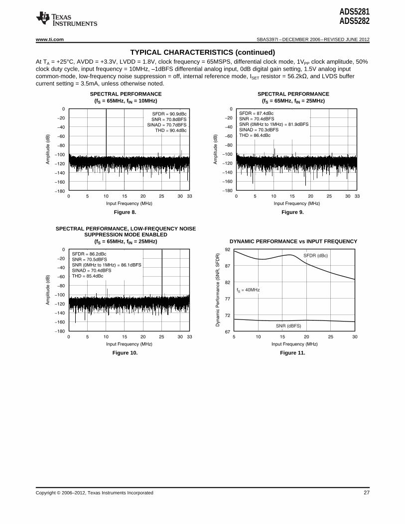
0
-20
-40
-60
-80
-100
-120
-140
-180
Input Frequency (MHz)
0 33
Am
plit
ude (
dB
)
2015105
-160
SFDR = 862dBc
SNR = 705dBFS
SNR (0MHz to 1MHz) = 861dBFS
SINAD = 704dBFS
THD = 854dBc
25 30
92
87
82
77
72
67
Input Frequency (MHz)
5 30
Dynam
ic P
erf
orm
ance (
SN
R S
FD
R)
201510 25
SNR (dBFS)
SFDR (dBc)
f = 40MHzS
0
-
-
-
-
-
-
-
-
-
20
40
60
80
100
120
140
160
180
Input Frequency (MHz)
0 33
Am
plit
ude (
dB
)
2015105 25 30
SFDR = 909dBc
SNR = 708dBFS
SINAD = 707dBFS
THD = 904dBc
0
-20
-40
-60
-80
-100
-120
-140
-180
Input Frequency (MHz)
0 33
Am
plit
ude (
dB
)
2015105
-160
SFDR = 874dBc
SNR = 704dBFS
SNR (0MHz to 1MHz) = 819dBFS
SINAD = 703dBFS
THD = 864dBc
25 30
ADS5281ADS5282
wwwticom SBAS397I ndashDECEMBER 2006ndashREVISED JUNE 2012
TYPICAL CHARACTERISTICS (continued)At TA = +25degC AVDD = +33V LVDD = 18V clock frequency = 65MSPS differential clock mode 1VPP clock amplitude 50clock duty cycle input frequency = 10MHz ndash1dBFS differential analog input 0dB digital gain setting 15V analog inputcommon-mode low-frequency noise suppression = off internal reference mode ISET resistor = 562kΩ and LVDS buffercurrent setting = 35mA unless otherwise noted
SPECTRAL PERFORMANCE SPECTRAL PERFORMANCE(fS = 65MHz fIN = 10MHz) (fS = 65MHz fIN = 25MHz)
Figure 8 Figure 9
SPECTRAL PERFORMANCE LOW-FREQUENCY NOISESUPPRESSION MODE ENABLED
(fS = 65MHz fIN = 25MHz) DYNAMIC PERFORMANCE vs INPUT FREQUENCY
Figure 10 Figure 11
Copyright copy 2006ndash2012 Texas Instruments Incorporated 27
95
85
75
65
55
45
35
25
Input Amplitude (dBFS)
Dyn
am
ic P
erf
orm
an
ce
(S
NR
S
FD
R)
SNR (dBFS)
SFDR (dBc)
f = 65MHz
f = 10MHzS
IN
-60 0-50 -40 -30 -20 -10
94
89
84
79
74
69
Clock Amplitude (V Differential)PP
06 23
Dynam
ic P
erf
orm
ance (
SN
R S
FD
R)
1611
SNR (dBFS)
SFDR (dBc)
f = 65MHz
f = 10MHzS
IN
21
95
90
85
80
75
70
65
60
Digital Gain (dB)
0 12
Dyn
am
ic P
erf
orm
an
ce
(S
NR
S
FD
R)
642 8
SNR (dBFS)
SFDR (dBc)
f = 65MHz
f = 10MHzS
IN
10
95
90
85
80
75
70
65
60
AVDD (V)
30 36
Dynam
ic P
erf
orm
ance (
SN
R S
FD
R)
333231 34
SNR (dBFS)
SFDR (dBc)
f = 65MHz
f = 10MHzS
IN
35
92
87
82
77
72
67
Input Frequency (MHz)
5 30
Dynam
ic P
erf
orm
ance (
SN
R S
FD
R)
201510 25
SNR (dBFS)
SFDR (dBc)
f = 50MHzS
97
92
87
82
77
72
67
Input Frequency (MHz)
5 30
Dynam
ic P
erf
orm
ance (
SN
R S
FD
R)
201510 25
SNR (dBFS)
SFDR (dBc)
f = 65MHzS
ADS5281ADS5282
SBAS397I ndashDECEMBER 2006ndashREVISED JUNE 2012 wwwticom
TYPICAL CHARACTERISTICS (continued)At TA = +25degC AVDD = +33V LVDD = 18V clock frequency = 65MSPS differential clock mode 1VPP clock amplitude 50clock duty cycle input frequency = 10MHz ndash1dBFS differential analog input 0dB digital gain setting 15V analog inputcommon-mode low-frequency noise suppression = off internal reference mode ISET resistor = 562kΩ and LVDS buffercurrent setting = 35mA unless otherwise noted
DYNAMIC PERFORMANCE vs INPUT FREQUENCY DYNAMIC PERFORMANCE vs INPUT FREQUENCY
Figure 12 Figure 13
DYNAMIC PERFORMANCE vs DIGITAL GAIN DYNAMIC PERFORMANCE vs AVDD
Figure 14 Figure 15
DYNAMIC PERFORMANCE vs INPUT AMPLITUDE DYNAMIC PERFORMANCE vs CLOCK AMPLITUDE
Figure 16 Figure 17
28 Copyright copy 2006ndash2012 Texas Instruments Incorporated
94
89
84
79
74
69
External Reference Common-Mode Voltage (REF + REF )2 (V)T B
135 165
Dynam
ic P
erf
orm
ance (
SN
R S
FD
R)
150145140
SNR (dBFS)
SFDR (dBc)
f = 65MHz
f = 10MHzS
IN
155 160
External reference differential voltage maintained at 2V
94
89
84
79
74
69
Voltage on V (V)CM
135 165
Dynam
ic P
erf
orm
ance (
SN
R S
FD
R)
150145140
SNR (dBFS)
SFDR (dBc)
f = 65MHz
f = 10MHzS
IN
155 160
94
89
84
79
74
69
Analog Input Common-Mode Voltage (V)
130 170
Dynam
ic P
erf
orm
ance (
SN
R S
FD
R)
140135
SNR (dBFS)
SFDR (dBc)
f = 65MHz
f = 10MHzS
IN
145 165160155150
94
89
84
79
74
69
External Reference Differential Voltage REF REF (V)-T B
16 24
Dynam
ic P
erf
orm
ance (
SN
R S
FD
R)
191817
SNR (dBFS)
SFDR (dBc)
f = 65MHz
f = 10MHzS
IN
20 232221
External reference common-mode voltage
maintained at 15V
ADS5281ADS5282
wwwticom SBAS397I ndashDECEMBER 2006ndashREVISED JUNE 2012
TYPICAL CHARACTERISTICS (continued)At TA = +25degC AVDD = +33V LVDD = 18V clock frequency = 65MSPS differential clock mode 1VPP clock amplitude 50clock duty cycle input frequency = 10MHz ndash1dBFS differential analog input 0dB digital gain setting 15V analog inputcommon-mode low-frequency noise suppression = off internal reference mode ISET resistor = 562kΩ and LVDS buffercurrent setting = 35mA unless otherwise noted
DYNAMIC PERFORMANCE vs ANALOG INPUT COMMON- DYNAMIC PERFORMANCE vs EXTERNAL REFERENCEMODE VOLTAGE DIFFERENTIAL VOLTAGE
Figure 18 Figure 19
DYNAMIC PERFORMANCE vs EXTERNAL REFERENCE DYNAMIC PERFORMANCE vs EXTERNAL REFERENCECOMMON-MODE VOLTAGE FORCED THROUGH VCM
Figure 20 Figure 21
Copyright copy 2006ndash2012 Texas Instruments Incorporated 29
05
04
03
02
01
0
-01
-02
-05
Code (LSB)
0 4096
INL
(L
SB
)
30722048 25601536 35841024512
-04
-03
f = 50MSPS
f = 5MHzS
IN
035
025
015
005
-005
-015
-035
Code (LSB)
0 4096
DN
L (
LS
B)
30722048 25601536 35841024512
-025
f = 50MSPS
f = 5MHzS
IN
60
50
40
30
20
10
0
Code Bin (LSB)
2049
Occurr
ence (
)
20532051 2054
f = 65MSPSS
2050 2052
0 0037 028
5192
4743
10
-10
-30
-50
-70
-90
-110
-130
-150
Input Frequency (MHz)
0 2 20
Am
plit
ude (
dB
)
1816141210864
f = 65MHz
f = 10MHz ( 7dBFS)
f = 161MHz ( 7dBFS)
IMD = 97dBFS
-
-
-
S
1
2
95
90
85
80
75
70
65
60
Clock Duty Cycle ()
35 65
Dynam
ic P
erf
orm
ance (
SN
R S
FD
R)
504540 55
SNR (dBFS)
SFDR (dBc)
f = 65MHz
f = 10MHzS
IN
60
95
85
80
75
70
60
Clock Duty Cycle ()
20 80
Dynam
ic P
erf
orm
ance (
SN
R S
FD
R)
504030 60
SNR (dBFS)
SFDR (dBc)
f = 65MHz
f = 10MHzS
IN
90
70
65
ADS5281ADS5282
SBAS397I ndashDECEMBER 2006ndashREVISED JUNE 2012 wwwticom
TYPICAL CHARACTERISTICS (continued)At TA = +25degC AVDD = +33V LVDD = 18V clock frequency = 65MSPS differential clock mode 1VPP clock amplitude 50clock duty cycle input frequency = 10MHz ndash1dBFS differential analog input 0dB digital gain setting 15V analog inputcommon-mode low-frequency noise suppression = off internal reference mode ISET resistor = 562kΩ and LVDS buffercurrent setting = 35mA unless otherwise noted
DYNAMIC PERFORMANCE vs CLOCK DUTY CYCLE DCC DYNAMIC PERFORMANCE vs CLOCK DUTY CYCLE DCCDISABLED ENABLED
Figure 22 Figure 23
HISTOGRAM OF OUTPUT CODE FOR ZERO INPUT INTERMODULATION DISTORTION
Figure 24 Figure 25
INTEGRAL NONLINEARITY DIFFERENTIAL NONLINEARITY
Figure 26 Figure 27
30 Copyright copy 2006ndash2012 Texas Instruments Incorporated
064
062
060
058
056
054
052
Sta
ndard
Devia
tion (
LS
B)
0 1 2 3 4 5 6
Overload Signal Amplitude (dBFS)
f = 65MSPS
f = 5MHzS
IN
Standard Deviation of
2nd Point After Overload
Standard Deviation of
1st Point After Overload
tS
16384 t (Group 1)S
Set 1 Point 1 (of 16) Set 1 Point 2 (of 16)
First point after overload (Set 1)
First point after overload (Set 2)
Second point after overload (Set 2)
Second point after overload (Set 1)
Overload
Amplitude
NOTES
Input sine wave phase is repetitive over 16384 clock cycles
16 such repetitive groups (of 16384 clock cycles) are capturedndasha total of 262144 points
Standard deviation of every set of are analyzed over the 16 groups
Worst case of all such standard deviations are plotted in the graphs
first and second points after overload
+FS
-FS
070
068
066
064
062
060
058
056
054
052
050
Sta
nd
ard
De
via
tio
n (
in L
SB
)
0 1 2 3 4 5 6
Overload Signal Amplitude (dBFS)
f = 50MSPS
f = 5MHzS
IN Standard Deviation of
2nd Point After Overload
Standard Deviation of
1st Point After Overload
170
130
110
90
70
30
Clock Frequency (MSPS)
5 75
I I
(mA
)A
VD
DLV
DD
352515 45
ILVDD
IAVDD
Zero Input on All Channels
Internal Reference Mode150
55
50
65
075
055
035
015
-005
-025
-065
Code (LSB)
0 4096
INL
(LS
B)
30722048 25601536 35841024512
-045
f = 65MSPS
f = 5MHzS
IN
035
025
015
005
-005
-015
-035
Code (LSB)
0 4096
DN
L (
LS
B)
30722048 25601536 35841024512
-025
f = 65MSPS f = 5MHzS IN
ADS5281ADS5282
wwwticom SBAS397I ndashDECEMBER 2006ndashREVISED JUNE 2012
TYPICAL CHARACTERISTICS (continued)At TA = +25degC AVDD = +33V LVDD = 18V clock frequency = 65MSPS differential clock mode 1VPP clock amplitude 50clock duty cycle input frequency = 10MHz ndash1dBFS differential analog input 0dB digital gain setting 15V analog inputcommon-mode low-frequency noise suppression = off internal reference mode ISET resistor = 562kΩ and LVDS buffercurrent setting = 35mA unless otherwise noted
INTEGRAL NONLINEARITY DIFFERENTIAL NONLINEARITY
Figure 28 Figure 29
AVDD AND LVDD POWER-SUPPLY CURRENTSvs CLOCK FREQUENCY OVERLOAD RECOVERY AT 50MSPS
Figure 30 Figure 31
OVERLOAD RECOVERY AT 65MSPS
Figure 32 Figure 33 Overload Recovery
Copyright copy 2006ndash2012 Texas Instruments Incorporated 31
ADS5281ADS5282
SBAS397I ndashDECEMBER 2006ndashREVISED JUNE 2012 wwwticom
APPLICATION INFORMATION
The ADC output goes to a serializer that operatesTHEORY OF OPERATION from a 12x clock generated by the PLL The 12 databits from each channel are serialized and sent LSBThe ADS528x devices are a family of 8-channelfirst In addition to serializing the data the serializerhigh-speed CMOS ADCs The 12 bits given out byalso generates a 1x clock and a 6x clock Theseeach channel are serialized and sent out on a singleclocks are generated in the same way the serializedpair of pins in LVDS format All eight channels of thedata are generated so these clocks maintain perfectADS528x operate from a single clock (ADCLK) Thesynchronization with the data The data and clocksampling clocks for each of the eight channels areoutputs of the serializer are buffered externally usinggenerated from the input clock using a carefullyLVDS buffers Using LVDS buffers to transmit datamatched clock buffer tree The 12x clock required forexternally has multiple advantages such as athe serializer is generated internally from ADCLKreduced number of output pins (saving routing spaceusing a phase-locked loop (PLL) A 6x and a 1x clockon the board) reduced power consumption andare also output in LVDS format along with the datareduced effects of digital noise coupling to the analogto enable easy data capture The ADS528x operatescircuit inside the ADS528xfrom internally-generated reference voltages that are
trimmed to improve to a high level of accuracy The ADS528x operates from two sets of supplies andTrimmed references improve the gain matching grounds The analog supply and ground set isacross devices and provide the option to operate the identified as AVDD and AVSS while the digital set isdevices without having to externally drive and route identified by LVDD and LVSSreference lines The nominal values of REFT andREFB are 25V and 05V respectively The ANALOG INPUTreferences are internally scaled down differentially bya factor of 2 This scaling results in a differential input The analog input consists of a switched-capacitorof ndash1V to correspond to the zero code of the ADC based differential sample-and-hold architecture Thisand a differential input of +1V to correspond to the differential topology results in very good acfull-scale code (4095 LSB) VCM (the common-mode performance even for high input frequencies at highvoltage of REFT and REFB) is also made available sampling rates The INN and INP pins must beexternally through a pin and is nominally 15V externally biased around a common-mode voltage of
15V available on VCM For a full-scale differentialThe ADC employs a pipelined converter architectureinput each input pin (INN and INP) must swingthat consists of a combination of multi-bit and single-symmetrically between VCM + 05V and VCM ndash 05Vbit internal stages Each stage feeds its data into theresulting in a 2VPP differential input swing Thedigital error correction logic ensuring excellentmaximum input peak-to-peak differential swing isdifferential linearity and no missing codes at the 12-determined to be the difference between the internalbit levelreference voltages REFT (25V nominal) and REFB(05V nominal) Figure 34 illustrates the model of theinput driving circuit
32 Copyright copy 2006ndash2012 Texas Instruments Incorporated
CM Buffer
Internal
Voltage
Reference
Input
Circuitry
INP
INN
VCM
12kW
12kW
ADS528x
(2mA) facute S
50MSPS
5nH to 9nH (TQFP-80)
2nH to 3nH (QFN-64)
15pF
to 24pF
IN OUT
INP
15pF to
25pF
1W
1000W
to 1440W
5W
to 10W
1000W
to 1440W
5nH to 9nH (TQFP-80)
2nH to 3nH (QFN-64)
INN
15pF to
25pF
1W
15W
to 25W
15W
to 30W
02pF
to 03pF
IN OUT
15pF
to 24pF
IN OUT
5W
to 10W
15W
to 25W
15W
to 30W
IN OUT
IN
OUT
16 to 32W W
IN OUT
IN OUT
OUTP
OUTN
Switches that are ON
in SAMPLE phase
Switches that are ON
in HOLD phase
ADS5281ADS5282
wwwticom SBAS397I ndashDECEMBER 2006ndashREVISED JUNE 2012
Figure 34 Analog Input Circuit Model
during ac-coupling by increasing VCM by roughlyInput Common-Mode Current 75mV When operating above 50MSPS it is
recommended that additional parallel resistors beThe input stage of all eight ADCs together sinks aadded externally to restore the input common-modecommon-mode current on the order of 2mA atto at least 14V if the inputs are to be ac-coupled50MSPS Equation 3 describes the dependency of
the common-mode current and the samplingfrequency
(3)
If the driving stage is dc-coupled to the inputs thenEquation 3 can be used to determine its common-mode drive capability and impedance The inputs canalso be ac-coupled to the INN and INP pins In thatcase the input common-mode is set by two internal12kΩ resistors connecting the input pins to VCM Thisarchitecture is shown in Figure 35
When the inputs are ac-coupled there is a drop inthe voltages at INP and INN relative to VCM This can Dashed area denotes one of eight channelsbe computed from Equation 3 At 50MSPS for
Figure 35 Common-Mode Biasing of Input Pinsexample the drop at each of the 16 input pins is150mV which is not optimal for ADC operationInitialization Registers 1 and 5 described in theInitialization Registers table can be used to partiallyreduce the effect of this input common-mode drop
Copyright copy 2006ndash2012 Texas Instruments Incorporated 33
01 Fm 50W
50W
200W
200W
INP
VCM
INN
01 Fm
12 21
47W
47W
01 Fm
01 Fm
25W
25W
11
INP
VCM
INN
ADS5281ADS5282
SBAS397I ndashDECEMBER 2006ndashREVISED JUNE 2012 wwwticom
Driving Circuit At high input frequencies the mismatch in thetransformer parasitic capacitance (between theFor optimum performance the analog inputs must bewindings) results in degraded even-order harmonicdriven differentially This approach improves theperformance Connecting two identical RFcommon-mode noise immunity and even-ordertransformers back-to-back helps to minimize thisharmonic rejection Input configurations using RFmismatch and good performance is obtained fortransformers suitable for low and high inputhigh-frequency input signals An additionalfrequencies are shown in Figure 36 and Figure 37termination resistor pair is required between the tworespectively The single-ended signal is fed to thetransformers as shown in Figure 37 The center pointprimary winding of the RF transformer Theof this termination is connected to ground to improvetransformer is terminated by 50Ω resistor on thethe balance between the positive and negative sidessecondary side Placing the termination on theThe values of the terminations between thesecondary side helps to shield the kicks caused bytransformers and on the secondary side must bethe input sampling capacitors from the RFchosen to achieve an overall 50Ω (in the case of 50Ωtransformer leakage inductances The termination issource impedance)accomplished by two 25Ω resistors connected in
series with the center point connected to the 15Vcommon-mode The 47Ω resistor in series with eachinput pin is required to damp the ringing caused bythe device package parasitics
Figure 36 Drive Circuit at Low Input Frequencies
Figure 37 Drive Circuit at High Input Frequencies
34 Copyright copy 2006ndash2012 Texas Instruments Incorporated
CLKP
CLKN
CMOS Clock Input
01 Fm
01 Fm
CLKP
CLKN
CMOS Single-Ended
Clock
0V
CLKP
CLKN
Differential Sine-Wave
PECL or LVDS Clock Input
01 Fm
01 Fm
5kW 5kW
VCM
CLKP
CLKN
VCM
ADS5281ADS5282
wwwticom SBAS397I ndashDECEMBER 2006ndashREVISED JUNE 2012
CLOCK INPUT
The eight channels on the device operate from asingle ADCLK input To ensure that the aperturedelay and jitter are the same for all channels a clocktree network is used to generate individual samplingclocks to each channel The clock paths for all thechannels are matched from the source point to thesampling circuit This architecture ensures that theperformance and timing for all channels are identicalThe use of the clock tree for matching introduces anaperture delay that is defined as the delay betweenthe rising edge of ADCLK and the actual instant ofsampling The aperture delays for all the channelsare matched to the best possible extent A mismatchof plusmn20ps (plusmn3σ) could exist between the apertureinstants of the eight ADCs within the same chip Figure 39 Internal Clock BufferHowever the aperture delays of ADCs across twodifferent chips can be several hundred picosecondsapart
The ADS528x can be made to operate either inCMOS single-ended clock mode (default isDIFF_CLK = 0) or differential clock mode (SINELVPECL or LVDS) When operating in the single-ended clock mode CLKN must be forced to 0VDCand the single-ended CMOS applied on the CLKP pinThis operation is shown in Figure 38
Figure 40 Differential Clock Driving Circuit(DIFF_CLK = 1)
Figure 38 Single-Ended Clock Driving Circuit(DIFF_CLK = 0)
When configured to operate in the differential clock Figure 41 Single-Ended Clock Driving Circuitmode (register bit DIFF_CLK = 1) the ADS528x clock When DIFF_CLK = 1inputs can be driven differentially (SINE LVPECL orLVDS) with little or no difference in performance
For best performance the clock inputs must bebetween them or with a single-ended (LVCMOS)driven differentially in order to reduce susceptibility toThe common-mode voltage of the clock inputs is setcommon-mode noise For high input frequencyto VCM using internal 5kΩ resistors as shown insampling it is recommended to use a clock sourceFigure 39 This method allows using transformer-with very low jitter Bandpass filtering of the clockcoupled drive circuits for a sine wave clock or ac-source can help reduce the effect of jitter If the dutycoupling for LVPECL and LVDS clock sources ascycle deviates from 50 by more than 2 or 3 it isshown in Figure 40 When operating in the differentialrecommended to enable the DCC through register bitclock mode the single-ended CMOS clock can be ac-EN_DCCcoupled to the CLKP input with CLKN (pin 11)
connected to ground with a 01μF capacitor asshown in Figure 41
Copyright copy 2006ndash2012 Texas Instruments Incorporated 35
Threshold 1 Threshold 2 Threshold 3
10 MHz 45 MHz 65 MHz
Sampling Frequency
ADS5281ADS5282
SBAS397I ndashDECEMBER 2006ndashREVISED JUNE 2012 wwwticom
PLL OPERATION ACROSS SAMPLING Step 2 Disable the PLL automatic switch and setFREQUENCY the PLL configuration depending on the clock
frequencyThe ADS528X uses a PLL for generating the highspeed bit clock (LCLK) the frame clock (ADCLK) amp SAMPLE CLOCK FREQUENCY REGISTER SETTING (Hex)internal clocks for the serializer operation RANGE (MSPS)
Min Max Address DataTo enable operation across the entire frequencyrange the PLL is automatically configured to one of 10 25 E3 0060four states depending on the sampling clock 15 45 E3 00A0frequency range The frequency range detection isautomatic and each time the sampling frequency With the above settings applied for the respectivecrosses a threshold the PLL changes its frequency ranges the part will continue toconfiguration to a new state To prevent unwanted operate as per the stated datasheet specificationstoggling of PLL state around a threshold the circuit for all timing parameters at all specifiedhas an inbuilt hysteresis The ADS528x has three frequencies EXCEPT for the timing specificationsthresholds ndash taking into account the hysteresis range at 40MSPS At 40MSPS the affected parametersof each threshold variation across devices and are ndash Data setup time Data hold time and Clocktemperature the thresholds can span the sampling propagation delay (refer to LVDS Timing )clock frequency range from 10MHz to 45MHz 2 For sampling clock frequency ge 45MSPS
As there are no PLL thresholds beyond 45MHzno change in PLL configuration can occur as thetemperature in the system stabilizes TheADS528x can be used in the system withoutusing the above software fix
INPUT OVER-VOLTAGE RECOVERY
The differential peak-to-peak full-scale rangesupported by the ADS528x is nominally 20V TheADS528x is specially designed to handle an over-
Figure 42 Variation of Thresholds Across voltage condition where the differential peak-to-peakSampling Frequency voltage can be up to twice the ADC full-scale range
If the input common-mode is not considerably offfrom VCM during overload (less than 300mV aroundBased on actual system clock frequency there arethe nominal value of 15V) recovery from an over-two scenariosvoltage pulse input of twice the amplitude of a full-1 For sampling clock frequency lt 45MSPSscale pulse is expected to be within one clock cycle
After system power up depending on the when the input switches from overload to zero signalfrequency of operation and the frequencythreshold for the given device the frequency REFERENCE CIRCUITrange detection circuit may change state once In
The digital beam-forming algorithm in an ultrasoundsome applications where a timing calibrationsystem relies on gain matching across all receivermight be done at the system level once afterchannels A typical system would have about 12 octalpower up this subsequent change of the PLLADCs on the board In such a case it is critical tostate might be undesirable as it can cause a lossensure that the gain is matched essentially requiringof alignment in the received data A software fixthe reference voltages seen by all the ADCs to be thefor eliminating this one-time change of PLL statesame Matching references within the eight channelsexists using the serial register interfaceof a chip is done by using a single internal referencendash Disable the automatic switch of the PLLvoltage buffer Trimming the reference voltages onconfiguration based on frequency detectedeach chip during production ensures that thendash In addition to disabling the switching it is alsoreference voltages are well-matched across differentrequired to set the PLL to the correctchipsconfiguration depending on the sample clock
frequency used in the system All bias currents required for the internal operation ofthe device are set using an external resistor toThe following sequence of register writes must beground at the ISET pin Using a 562kΩ resistor on ISETfollowedgenerates an internal reference current of 20μA This
Step 1 Write Address = 0x01 Data = 0x0010 current is mirrored internally to generate the biascurrent for the internal blocks Using a larger external
36 Copyright copy 2006ndash2012 Texas Instruments Incorporated
VREF = 15V -B
VCM
15V
VREF = 15V +T
VCM
15V
REFT
REFB
ISET
01 Fm 22 Fm
0 to
2
W
W
0 toW
2W
562kW
22 Fm 01 Fm
ADS528x
ADS5281ADS5282
wwwticom SBAS397I ndashDECEMBER 2006ndashREVISED JUNE 2012
resistor at ISET reduces the reference bias current and The device also supports the use of externalthereby scales down the device operating power reference voltages There are two methods to forceHowever it is recommended that the external resistor the references externally The first method involvesbe within 10 of the specified value of 562kΩ so pulling INTEXT low and forcing externally REFT andthat the internal bias margins for the various blocks REFB to 25V and 05V nominally respectively In thisare proper mode the internal reference buffer goes to a 3-state
output The external reference driving circuit shouldBuffering the internal bandgap voltage also generates be designed to provide the required switching currentthe common-mode voltage VCM which is set to the for the eight ADCs inside the chip It should be notedmidlevel of REFT and REFB and is accessible on a that in this mode VCM and ISET continue to bepin (pin 65 in TQFP-80 package pin 53 in QFN-64 generated from the internal bandgap voltage as inpackage) It is meant as a reference voltage to derive the internal reference mode It is therefore importantthe input common-mode if the input is directly to ensure that the common-mode voltage of thecoupled It can also be used to derive the reference externally-forced reference voltages matches tocommon-mode voltage in the external reference within 50mV of VCMmode The suggested decoupling for the referencepins is shown in Figure 43 The second method of forcing the reference voltages
externally can be accessed by pulling INTEXT lowand programming the serial interface to drive theexternal reference mode through the VCM pin (registerbit called EXT_REF_VCM) In this mode VCMbecomes configured as an input pin that can bedriven from external circuitry The internal referencebuffers driving REFT and REFB are active in thismode Forcing 15V on the VCM pin in the moderesults in REFT and REFB coming to 25V and 05Vrespectively In general the voltages on REFT andREFB in this mode are given by Equation 4 andEquation 5 respectively
(4)Figure 43 Suggested Decoupling on the
Reference Pins(5)
The state of the reference voltage internal buffersduring various combinations of the PD INTEXT andEXT_REF_VCM register bits is described in Table 8
Table 8 State of Reference Voltages for Various Combinations of PD INTEXT and EXT_REF_VCM
REGISTER BIT INTERNAL BUFFER STATE
PD 0 0 1 1 0 0 1 1
INTEXT 0 1 0 1 0 1 0 1
EXT_REF_VCM 0 0 0 0 1 1 1 1
REFT buffer 3-state 25V 3-state 25V (1) 15V + VCM15V Do not use 25V (1) Do not use
REFB buffer 3-state 05V 3-state 05V (1) 15V ndash VCM15V Do not use 05V (1) Do not use
VCM pin 15V 15V 15V 15V Force Do not use Force Do not use
(1) Weakly forced with reduced strengthsections while LVDD and LVSS are used to denotethe digital supplies Care is taken to ensure that thereNOISE COUPLING ISSUESis minimal interaction between the supply sets within
High-speed mixed signals are sensitive to various the device The extent of noise coupled andtypes of noise coupling One primary source of noise transmitted from the digital to the analog sectionsis the switching noise from the serializer and the depends onoutput buffers Maximum care is taken to isolate
1 The effective inductances of each of the supplythese noise sources from the sensitive analog blocksand ground setsAs a starting point the analog and digital domains of
2 The isolation between the digital and analogthe device are clearly demarcated AVDD and AVSSsupply and ground setsare used to denote the supplies for the analog
Copyright copy 2006ndash2012 Texas Instruments Incorporated 37
ADS5281ADS5282
SBAS397I ndashDECEMBER 2006ndashREVISED JUNE 2012 wwwticom
Smaller effective inductance of the supply and ground It is recommended that the isolation be maintained onpins leads to better noise suppression For this the board by using separate supplies to drive AVDDreason multiple pins are used to drive each supply and LVDD as well as separate ground planes forand ground It is also critical to ensure that the AVSS and LVSS The use of LVDS buffers reducesimpedances of the supply and ground lines on the the injected noise considerably compared to CMOSboard are kept to the minimum possible values Use buffers The current in the LVDS buffer isof ground planes in the printed circuit board (PCB) as independent of the direction of switching Also thewell as large decoupling capacitors between the low output swing as well as the differential nature ofsupply and ground lines are necessary to obtain the the LVDS buffer results in low-noise couplingbest possible SNR performance from the device
38 Copyright copy 2006ndash2012 Texas Instruments Incorporated
ADS5281ADS5282
wwwticom SBAS397I ndashDECEMBER 2006ndashREVISED JUNE 2012
REVISION HISTORY
Changes from Revision G (March 2008) to Revision H Page
bull Changed second table and conditions in the Initialization Registers section 3
bull Changed In Input Common-Mode Current section changed initialization register 5 to initialization registers 1 and 5to reflect change in Initialization Registers table 33
Changes from Revision F (March 2008) to Revision G Page
bull Deleted note (3) of Ordering Information table to indicate device status is now Production Data for all parts 2
bull Added new note (3) of Ordering Information table to indicate the quantity of transport media is available in thePackage Option Addendum 2
bull Added note (1) to Initialization Registers section to indicate it is no longer necessary to program initializationregisters 1 to 4 3
bull Changed maximum specifications for ADS5282 column in the Power SupplymdashInternal Reference Mode section ofElectrical Characteristics (By Device) table 6
bull Changed minimum specification for ADS5282 column in the f = 10 MHz row of the SNR section of ElectricalCharacteristics (By Device) table 6
Changes from Revision H (March 2008) to Revision I Page
bull Added table in the INITIALIZATION REGISTERS section 3
bull Added table in the LVDS OUTPUT TIMING CHARACTERISTICS section 14
bull Added PLL OPERATION ACROSS SAMPLING FREQUENCY section 36
Copyright copy 2006ndash2012 Texas Instruments Incorporated 39
PACKAGE OPTION ADDENDUM
wwwticom 26-Oct-2016
Addendum-Page 1
PACKAGING INFORMATION
Orderable Device Status(1)
Package Type PackageDrawing
Pins PackageQty
Eco Plan(2)
LeadBall Finish(6)
MSL Peak Temp(3)
Op Temp (degC) Device Marking(45)
Samples
ADS5281IPFP ACTIVE HTQFP PFP 80 96 Green (RoHSamp no SbBr)
CU NIPDAU Level-3-260C-168 HR -40 to 85 ADS5281I
ADS5281IPFPR ACTIVE HTQFP PFP 80 1000 Green (RoHSamp no SbBr)
CU NIPDAU Level-3-260C-168 HR -40 to 85 ADS5281I
ADS5281IRGCR ACTIVE VQFN RGC 64 2000 Green (RoHSamp no SbBr)
CU NIPDAU Level-3-260C-168 HR -40 to 85 AZ5281
ADS5281IRGCT ACTIVE VQFN RGC 64 250 Green (RoHSamp no SbBr)
CU NIPDAU Level-3-260C-168 HR -40 to 85 AZ5281
ADS5282IRGCR ACTIVE VQFN RGC 64 2000 Green (RoHSamp no SbBr)
CU NIPDAU Level-3-260C-168 HR -40 to 85 AZ5282
ADS5282IRGCT ACTIVE VQFN RGC 64 250 Green (RoHSamp no SbBr)
CU NIPDAU Level-3-260C-168 HR -40 to 85 AZ5282
(1) The marketing status values are defined as followsACTIVE Product device recommended for new designsLIFEBUY TI has announced that the device will be discontinued and a lifetime-buy period is in effectNRND Not recommended for new designs Device is in production to support existing customers but TI does not recommend using this part in a new designPREVIEW Device has been announced but is not in production Samples may or may not be availableOBSOLETE TI has discontinued the production of the device
(2) Eco Plan - The planned eco-friendly classification Pb-Free (RoHS) Pb-Free (RoHS Exempt) or Green (RoHS amp no SbBr) - please check httpwwwticomproductcontent for the latest availabilityinformation and additional product content detailsTBD The Pb-FreeGreen conversion plan has not been definedPb-Free (RoHS) TIs terms Lead-Free or Pb-Free mean semiconductor products that are compatible with the current RoHS requirements for all 6 substances including the requirement thatlead not exceed 01 by weight in homogeneous materials Where designed to be soldered at high temperatures TI Pb-Free products are suitable for use in specified lead-free processesPb-Free (RoHS Exempt) This component has a RoHS exemption for either 1) lead-based flip-chip solder bumps used between the die and package or 2) lead-based die adhesive used betweenthe die and leadframe The component is otherwise considered Pb-Free (RoHS compatible) as defined aboveGreen (RoHS amp no SbBr) TI defines Green to mean Pb-Free (RoHS compatible) and free of Bromine (Br) and Antimony (Sb) based flame retardants (Br or Sb do not exceed 01 by weightin homogeneous material)
(3) MSL Peak Temp - The Moisture Sensitivity Level rating according to the JEDEC industry standard classifications and peak solder temperature
(4) There may be additional marking which relates to the logo the lot trace code information or the environmental category on the device
(5) Multiple Device Markings will be inside parentheses Only one Device Marking contained in parentheses and separated by a ~ will appear on a device If a line is indented then it is a continuationof the previous line and the two combined represent the entire Device Marking for that device
PACKAGE OPTION ADDENDUM
wwwticom 26-Oct-2016
Addendum-Page 2
(6) LeadBall Finish - Orderable Devices may have multiple material finish options Finish options are separated by a vertical ruled line LeadBall Finish values may wrap to two lines if the finishvalue exceeds the maximum column width
Important Information and DisclaimerThe information provided on this page represents TIs knowledge and belief as of the date that it is provided TI bases its knowledge and belief on informationprovided by third parties and makes no representation or warranty as to the accuracy of such information Efforts are underway to better integrate information from third parties TI has taken andcontinues to take reasonable steps to provide representative and accurate information but may not have conducted destructive testing or chemical analysis on incoming materials and chemicalsTI and TI suppliers consider certain information to be proprietary and thus CAS numbers and other limited information may not be available for release
In no event shall TIs liability arising out of such information exceed the total purchase price of the TI part(s) at issue in this document sold by TI to Customer on an annual basis
TAPE AND REEL INFORMATION
All dimensions are nominal
Device PackageType
PackageDrawing
Pins SPQ ReelDiameter
(mm)
ReelWidth
W1 (mm)
A0(mm)
B0(mm)
K0(mm)
P1(mm)
W(mm)
Pin1Quadrant
ADS5281IPFPR HTQFP PFP 80 1000 3300 244 150 150 15 200 240 Q2
ADS5281IRGCR VQFN RGC 64 2000 3300 164 93 93 15 120 160 Q2
ADS5281IRGCT VQFN RGC 64 250 1800 164 93 93 15 120 160 Q2
ADS5282IRGCR VQFN RGC 64 2000 3300 164 93 93 15 120 160 Q2
ADS5282IRGCT VQFN RGC 64 250 1800 164 93 93 15 120 160 Q2
PACKAGE MATERIALS INFORMATION
wwwticom 14-May-2015
Pack Materials-Page 1
All dimensions are nominal
Device Package Type Package Drawing Pins SPQ Length (mm) Width (mm) Height (mm)
ADS5281IPFPR HTQFP PFP 80 1000 3670 3670 450
ADS5281IRGCR VQFN RGC 64 2000 3366 3366 286
ADS5281IRGCT VQFN RGC 64 250 2130 1910 550
ADS5282IRGCR VQFN RGC 64 2000 3366 3366 286
ADS5282IRGCT VQFN RGC 64 250 2130 1910 550
PACKAGE MATERIALS INFORMATION
wwwticom 14-May-2015
Pack Materials-Page 2
wwwticom
IMPORTANT NOTICE
Texas Instruments Incorporated and its subsidiaries (TI) reserve the right to make corrections enhancements improvements and otherchanges to its semiconductor products and services per JESD46 latest issue and to discontinue any product or service per JESD48 latestissue Buyers should obtain the latest relevant information before placing orders and should verify that such information is current andcomplete All semiconductor products (also referred to herein as ldquocomponentsrdquo) are sold subject to TIrsquos terms and conditions of salesupplied at the time of order acknowledgmentTI warrants performance of its components to the specifications applicable at the time of sale in accordance with the warranty in TIrsquos termsand conditions of sale of semiconductor products Testing and other quality control techniques are used to the extent TI deems necessaryto support this warranty Except where mandated by applicable law testing of all parameters of each component is not necessarilyperformedTI assumes no liability for applications assistance or the design of Buyersrsquo products Buyers are responsible for their products andapplications using TI components To minimize the risks associated with Buyersrsquo products and applications Buyers should provideadequate design and operating safeguardsTI does not warrant or represent that any license either express or implied is granted under any patent right copyright mask work right orother intellectual property right relating to any combination machine or process in which TI components or services are used Informationpublished by TI regarding third-party products or services does not constitute a license to use such products or services or a warranty orendorsement thereof Use of such information may require a license from a third party under the patents or other intellectual property of thethird party or a license from TI under the patents or other intellectual property of TIReproduction of significant portions of TI information in TI data books or data sheets is permissible only if reproduction is without alterationand is accompanied by all associated warranties conditions limitations and notices TI is not responsible or liable for such altereddocumentation Information of third parties may be subject to additional restrictionsResale of TI components or services with statements different from or beyond the parameters stated by TI for that component or servicevoids all express and any implied warranties for the associated TI component or service and is an unfair and deceptive business practiceTI is not responsible or liable for any such statementsBuyer acknowledges and agrees that it is solely responsible for compliance with all legal regulatory and safety-related requirementsconcerning its products and any use of TI components in its applications notwithstanding any applications-related information or supportthat may be provided by TI Buyer represents and agrees that it has all the necessary expertise to create and implement safeguards whichanticipate dangerous consequences of failures monitor failures and their consequences lessen the likelihood of failures that might causeharm and take appropriate remedial actions Buyer will fully indemnify TI and its representatives against any damages arising out of the useof any TI components in safety-critical applicationsIn some cases TI components may be promoted specifically to facilitate safety-related applications With such components TIrsquos goal is tohelp enable customers to design and create their own end-product solutions that meet applicable functional safety standards andrequirements Nonetheless such components are subject to these termsNo TI components are authorized for use in FDA Class III (or similar life-critical medical equipment) unless authorized officers of the partieshave executed a special agreement specifically governing such useOnly those TI components which TI has specifically designated as military grade or ldquoenhanced plasticrdquo are designed and intended for use inmilitaryaerospace applications or environments Buyer acknowledges and agrees that any military or aerospace use of TI componentswhich have not been so designated is solely at the Buyers risk and that Buyer is solely responsible for compliance with all legal andregulatory requirements in connection with such useTI has specifically designated certain components as meeting ISOTS16949 requirements mainly for automotive use In any case of use ofnon-designated products TI will not be responsible for any failure to meet ISOTS16949
Products ApplicationsAudio wwwticomaudio Automotive and Transportation wwwticomautomotiveAmplifiers amplifierticom Communications and Telecom wwwticomcommunicationsData Converters dataconverterticom Computers and Peripherals wwwticomcomputersDLPreg Products wwwdlpcom Consumer Electronics wwwticomconsumer-appsDSP dspticom Energy and Lighting wwwticomenergyClocks and Timers wwwticomclocks Industrial wwwticomindustrialInterface interfaceticom Medical wwwticommedicalLogic logicticom Security wwwticomsecurityPower Mgmt powerticom Space Avionics and Defense wwwticomspace-avionics-defenseMicrocontrollers microcontrollerticom Video and Imaging wwwticomvideoRFID wwwti-rfidcomOMAP Applications Processors wwwticomomap TI E2E Community e2eticomWireless Connectivity wwwticomwirelessconnectivity
Mailing Address Texas Instruments Post Office Box 655303 Dallas Texas 75265Copyright copy 2016 Texas Instruments Incorporated
- FEATURES
- APPLICATIONS
- DESCRIPTION
- ABSOLUTE MAXIMUM RATINGS
- RECOMMENDED OPERATING CONDITIONS
- INITIALIZATION REGISTERS
- DIGITAL CHARACTERISTICS
- ELECTRICAL CHARACTERISTICS
- ELECTRICAL CHARACTERISTICS (BY DEVICE)
- PIN CONFIGURATIONS
- FUNCTIONAL BLOCK DIAGRAM
- TIMING CHARACTERISTICS
- LVDS OUTPUT TIMING CHARACTERISTICS
- LVDS OUTPUT TIMING CHARACTERISTICS
- LVDS OUTPUT TIMING CHARACTERISTICS
- SERIAL INTERFACE
-
- Register Initialization
-
- SERIAL REGISTER MAP
- SUMMARY OF FEATURES
- DESCRIPTION OF SERIAL REGISTERS
-
- SOFTWARE RESET
- POWER-DOWN MODES
- LVDS DRIVE PROGRAMMABILITY
- LVDS INTERNAL TERMINATION PROGRAMMABILITY
- LOW-FREQUENCY NOISE SUPPRESSION MODE
- ANALOG INPUT INVERT
- LVDS TEST PATTERNS
- PROGRAMMABLE GAIN
- CLOCK REFERENCE AND DATA OUTPUT MODES
-
- INPUT CLOCK
- EXTERNAL REFERENCE
- BIT CLOCK PROGRAMMABILITY
- DATA OUTPUT FORMAT MODES
-
- TYPICAL CHARACTERISTICS
- APPLICATION INFORMATION
-
- THEORY OF OPERATION
- ANALOG INPUT
-
- Input Common-Mode Current
- Driving Circuit
-
- CLOCK INPUT
- PLL OPERATION ACROSS SAMPLING FREQUENCY
- INPUT OVER-VOLTAGE RECOVERY
- REFERENCE CIRCUIT
- NOISE COUPLING ISSUES
-
- Revision History
-

95
85
75
65
55
45
35
25
Input Amplitude (dBFS)
Dyn
am
ic P
erf
orm
an
ce
(S
NR
S
FD
R)
SNR (dBFS)
SFDR (dBc)
f = 65MHz
f = 10MHzS
IN
-60 0-50 -40 -30 -20 -10
94
89
84
79
74
69
Clock Amplitude (V Differential)PP
06 23
Dynam
ic P
erf
orm
ance (
SN
R S
FD
R)
1611
SNR (dBFS)
SFDR (dBc)
f = 65MHz
f = 10MHzS
IN
21
95
90
85
80
75
70
65
60
Digital Gain (dB)
0 12
Dyn
am
ic P
erf
orm
an
ce
(S
NR
S
FD
R)
642 8
SNR (dBFS)
SFDR (dBc)
f = 65MHz
f = 10MHzS
IN
10
95
90
85
80
75
70
65
60
AVDD (V)
30 36
Dynam
ic P
erf
orm
ance (
SN
R S
FD
R)
333231 34
SNR (dBFS)
SFDR (dBc)
f = 65MHz
f = 10MHzS
IN
35
92
87
82
77
72
67
Input Frequency (MHz)
5 30
Dynam
ic P
erf
orm
ance (
SN
R S
FD
R)
201510 25
SNR (dBFS)
SFDR (dBc)
f = 50MHzS
97
92
87
82
77
72
67
Input Frequency (MHz)
5 30
Dynam
ic P
erf
orm
ance (
SN
R S
FD
R)
201510 25
SNR (dBFS)
SFDR (dBc)
f = 65MHzS
ADS5281ADS5282
SBAS397I ndashDECEMBER 2006ndashREVISED JUNE 2012 wwwticom
TYPICAL CHARACTERISTICS (continued)At TA = +25degC AVDD = +33V LVDD = 18V clock frequency = 65MSPS differential clock mode 1VPP clock amplitude 50clock duty cycle input frequency = 10MHz ndash1dBFS differential analog input 0dB digital gain setting 15V analog inputcommon-mode low-frequency noise suppression = off internal reference mode ISET resistor = 562kΩ and LVDS buffercurrent setting = 35mA unless otherwise noted
DYNAMIC PERFORMANCE vs INPUT FREQUENCY DYNAMIC PERFORMANCE vs INPUT FREQUENCY
Figure 12 Figure 13
DYNAMIC PERFORMANCE vs DIGITAL GAIN DYNAMIC PERFORMANCE vs AVDD
Figure 14 Figure 15
DYNAMIC PERFORMANCE vs INPUT AMPLITUDE DYNAMIC PERFORMANCE vs CLOCK AMPLITUDE
Figure 16 Figure 17
28 Copyright copy 2006ndash2012 Texas Instruments Incorporated
94
89
84
79
74
69
External Reference Common-Mode Voltage (REF + REF )2 (V)T B
135 165
Dynam
ic P
erf
orm
ance (
SN
R S
FD
R)
150145140
SNR (dBFS)
SFDR (dBc)
f = 65MHz
f = 10MHzS
IN
155 160
External reference differential voltage maintained at 2V
94
89
84
79
74
69
Voltage on V (V)CM
135 165
Dynam
ic P
erf
orm
ance (
SN
R S
FD
R)
150145140
SNR (dBFS)
SFDR (dBc)
f = 65MHz
f = 10MHzS
IN
155 160
94
89
84
79
74
69
Analog Input Common-Mode Voltage (V)
130 170
Dynam
ic P
erf
orm
ance (
SN
R S
FD
R)
140135
SNR (dBFS)
SFDR (dBc)
f = 65MHz
f = 10MHzS
IN
145 165160155150
94
89
84
79
74
69
External Reference Differential Voltage REF REF (V)-T B
16 24
Dynam
ic P
erf
orm
ance (
SN
R S
FD
R)
191817
SNR (dBFS)
SFDR (dBc)
f = 65MHz
f = 10MHzS
IN
20 232221
External reference common-mode voltage
maintained at 15V
ADS5281ADS5282
wwwticom SBAS397I ndashDECEMBER 2006ndashREVISED JUNE 2012
TYPICAL CHARACTERISTICS (continued)At TA = +25degC AVDD = +33V LVDD = 18V clock frequency = 65MSPS differential clock mode 1VPP clock amplitude 50clock duty cycle input frequency = 10MHz ndash1dBFS differential analog input 0dB digital gain setting 15V analog inputcommon-mode low-frequency noise suppression = off internal reference mode ISET resistor = 562kΩ and LVDS buffercurrent setting = 35mA unless otherwise noted
DYNAMIC PERFORMANCE vs ANALOG INPUT COMMON- DYNAMIC PERFORMANCE vs EXTERNAL REFERENCEMODE VOLTAGE DIFFERENTIAL VOLTAGE
Figure 18 Figure 19
DYNAMIC PERFORMANCE vs EXTERNAL REFERENCE DYNAMIC PERFORMANCE vs EXTERNAL REFERENCECOMMON-MODE VOLTAGE FORCED THROUGH VCM
Figure 20 Figure 21
Copyright copy 2006ndash2012 Texas Instruments Incorporated 29
05
04
03
02
01
0
-01
-02
-05
Code (LSB)
0 4096
INL
(L
SB
)
30722048 25601536 35841024512
-04
-03
f = 50MSPS
f = 5MHzS
IN
035
025
015
005
-005
-015
-035
Code (LSB)
0 4096
DN
L (
LS
B)
30722048 25601536 35841024512
-025
f = 50MSPS
f = 5MHzS
IN
60
50
40
30
20
10
0
Code Bin (LSB)
2049
Occurr
ence (
)
20532051 2054
f = 65MSPSS
2050 2052
0 0037 028
5192
4743
10
-10
-30
-50
-70
-90
-110
-130
-150
Input Frequency (MHz)
0 2 20
Am
plit
ude (
dB
)
1816141210864
f = 65MHz
f = 10MHz ( 7dBFS)
f = 161MHz ( 7dBFS)
IMD = 97dBFS
-
-
-
S
1
2
95
90
85
80
75
70
65
60
Clock Duty Cycle ()
35 65
Dynam
ic P
erf
orm
ance (
SN
R S
FD
R)
504540 55
SNR (dBFS)
SFDR (dBc)
f = 65MHz
f = 10MHzS
IN
60
95
85
80
75
70
60
Clock Duty Cycle ()
20 80
Dynam
ic P
erf
orm
ance (
SN
R S
FD
R)
504030 60
SNR (dBFS)
SFDR (dBc)
f = 65MHz
f = 10MHzS
IN
90
70
65
ADS5281ADS5282
SBAS397I ndashDECEMBER 2006ndashREVISED JUNE 2012 wwwticom
TYPICAL CHARACTERISTICS (continued)At TA = +25degC AVDD = +33V LVDD = 18V clock frequency = 65MSPS differential clock mode 1VPP clock amplitude 50clock duty cycle input frequency = 10MHz ndash1dBFS differential analog input 0dB digital gain setting 15V analog inputcommon-mode low-frequency noise suppression = off internal reference mode ISET resistor = 562kΩ and LVDS buffercurrent setting = 35mA unless otherwise noted
DYNAMIC PERFORMANCE vs CLOCK DUTY CYCLE DCC DYNAMIC PERFORMANCE vs CLOCK DUTY CYCLE DCCDISABLED ENABLED
Figure 22 Figure 23
HISTOGRAM OF OUTPUT CODE FOR ZERO INPUT INTERMODULATION DISTORTION
Figure 24 Figure 25
INTEGRAL NONLINEARITY DIFFERENTIAL NONLINEARITY
Figure 26 Figure 27
30 Copyright copy 2006ndash2012 Texas Instruments Incorporated
064
062
060
058
056
054
052
Sta
ndard
Devia
tion (
LS
B)
0 1 2 3 4 5 6
Overload Signal Amplitude (dBFS)
f = 65MSPS
f = 5MHzS
IN
Standard Deviation of
2nd Point After Overload
Standard Deviation of
1st Point After Overload
tS
16384 t (Group 1)S
Set 1 Point 1 (of 16) Set 1 Point 2 (of 16)
First point after overload (Set 1)
First point after overload (Set 2)
Second point after overload (Set 2)
Second point after overload (Set 1)
Overload
Amplitude
NOTES
Input sine wave phase is repetitive over 16384 clock cycles
16 such repetitive groups (of 16384 clock cycles) are capturedndasha total of 262144 points
Standard deviation of every set of are analyzed over the 16 groups
Worst case of all such standard deviations are plotted in the graphs
first and second points after overload
+FS
-FS
070
068
066
064
062
060
058
056
054
052
050
Sta
nd
ard
De
via
tio
n (
in L
SB
)
0 1 2 3 4 5 6
Overload Signal Amplitude (dBFS)
f = 50MSPS
f = 5MHzS
IN Standard Deviation of
2nd Point After Overload
Standard Deviation of
1st Point After Overload
170
130
110
90
70
30
Clock Frequency (MSPS)
5 75
I I
(mA
)A
VD
DLV
DD
352515 45
ILVDD
IAVDD
Zero Input on All Channels
Internal Reference Mode150
55
50
65
075
055
035
015
-005
-025
-065
Code (LSB)
0 4096
INL
(LS
B)
30722048 25601536 35841024512
-045
f = 65MSPS
f = 5MHzS
IN
035
025
015
005
-005
-015
-035
Code (LSB)
0 4096
DN
L (
LS
B)
30722048 25601536 35841024512
-025
f = 65MSPS f = 5MHzS IN
ADS5281ADS5282
wwwticom SBAS397I ndashDECEMBER 2006ndashREVISED JUNE 2012
TYPICAL CHARACTERISTICS (continued)At TA = +25degC AVDD = +33V LVDD = 18V clock frequency = 65MSPS differential clock mode 1VPP clock amplitude 50clock duty cycle input frequency = 10MHz ndash1dBFS differential analog input 0dB digital gain setting 15V analog inputcommon-mode low-frequency noise suppression = off internal reference mode ISET resistor = 562kΩ and LVDS buffercurrent setting = 35mA unless otherwise noted
INTEGRAL NONLINEARITY DIFFERENTIAL NONLINEARITY
Figure 28 Figure 29
AVDD AND LVDD POWER-SUPPLY CURRENTSvs CLOCK FREQUENCY OVERLOAD RECOVERY AT 50MSPS
Figure 30 Figure 31
OVERLOAD RECOVERY AT 65MSPS
Figure 32 Figure 33 Overload Recovery
Copyright copy 2006ndash2012 Texas Instruments Incorporated 31
ADS5281ADS5282
SBAS397I ndashDECEMBER 2006ndashREVISED JUNE 2012 wwwticom
APPLICATION INFORMATION
The ADC output goes to a serializer that operatesTHEORY OF OPERATION from a 12x clock generated by the PLL The 12 databits from each channel are serialized and sent LSBThe ADS528x devices are a family of 8-channelfirst In addition to serializing the data the serializerhigh-speed CMOS ADCs The 12 bits given out byalso generates a 1x clock and a 6x clock Theseeach channel are serialized and sent out on a singleclocks are generated in the same way the serializedpair of pins in LVDS format All eight channels of thedata are generated so these clocks maintain perfectADS528x operate from a single clock (ADCLK) Thesynchronization with the data The data and clocksampling clocks for each of the eight channels areoutputs of the serializer are buffered externally usinggenerated from the input clock using a carefullyLVDS buffers Using LVDS buffers to transmit datamatched clock buffer tree The 12x clock required forexternally has multiple advantages such as athe serializer is generated internally from ADCLKreduced number of output pins (saving routing spaceusing a phase-locked loop (PLL) A 6x and a 1x clockon the board) reduced power consumption andare also output in LVDS format along with the datareduced effects of digital noise coupling to the analogto enable easy data capture The ADS528x operatescircuit inside the ADS528xfrom internally-generated reference voltages that are
trimmed to improve to a high level of accuracy The ADS528x operates from two sets of supplies andTrimmed references improve the gain matching grounds The analog supply and ground set isacross devices and provide the option to operate the identified as AVDD and AVSS while the digital set isdevices without having to externally drive and route identified by LVDD and LVSSreference lines The nominal values of REFT andREFB are 25V and 05V respectively The ANALOG INPUTreferences are internally scaled down differentially bya factor of 2 This scaling results in a differential input The analog input consists of a switched-capacitorof ndash1V to correspond to the zero code of the ADC based differential sample-and-hold architecture Thisand a differential input of +1V to correspond to the differential topology results in very good acfull-scale code (4095 LSB) VCM (the common-mode performance even for high input frequencies at highvoltage of REFT and REFB) is also made available sampling rates The INN and INP pins must beexternally through a pin and is nominally 15V externally biased around a common-mode voltage of
15V available on VCM For a full-scale differentialThe ADC employs a pipelined converter architectureinput each input pin (INN and INP) must swingthat consists of a combination of multi-bit and single-symmetrically between VCM + 05V and VCM ndash 05Vbit internal stages Each stage feeds its data into theresulting in a 2VPP differential input swing Thedigital error correction logic ensuring excellentmaximum input peak-to-peak differential swing isdifferential linearity and no missing codes at the 12-determined to be the difference between the internalbit levelreference voltages REFT (25V nominal) and REFB(05V nominal) Figure 34 illustrates the model of theinput driving circuit
32 Copyright copy 2006ndash2012 Texas Instruments Incorporated
CM Buffer
Internal
Voltage
Reference
Input
Circuitry
INP
INN
VCM
12kW
12kW
ADS528x
(2mA) facute S
50MSPS
5nH to 9nH (TQFP-80)
2nH to 3nH (QFN-64)
15pF
to 24pF
IN OUT
INP
15pF to
25pF
1W
1000W
to 1440W
5W
to 10W
1000W
to 1440W
5nH to 9nH (TQFP-80)
2nH to 3nH (QFN-64)
INN
15pF to
25pF
1W
15W
to 25W
15W
to 30W
02pF
to 03pF
IN OUT
15pF
to 24pF
IN OUT
5W
to 10W
15W
to 25W
15W
to 30W
IN OUT
IN
OUT
16 to 32W W
IN OUT
IN OUT
OUTP
OUTN
Switches that are ON
in SAMPLE phase
Switches that are ON
in HOLD phase
ADS5281ADS5282
wwwticom SBAS397I ndashDECEMBER 2006ndashREVISED JUNE 2012
Figure 34 Analog Input Circuit Model
during ac-coupling by increasing VCM by roughlyInput Common-Mode Current 75mV When operating above 50MSPS it is
recommended that additional parallel resistors beThe input stage of all eight ADCs together sinks aadded externally to restore the input common-modecommon-mode current on the order of 2mA atto at least 14V if the inputs are to be ac-coupled50MSPS Equation 3 describes the dependency of
the common-mode current and the samplingfrequency
(3)
If the driving stage is dc-coupled to the inputs thenEquation 3 can be used to determine its common-mode drive capability and impedance The inputs canalso be ac-coupled to the INN and INP pins In thatcase the input common-mode is set by two internal12kΩ resistors connecting the input pins to VCM Thisarchitecture is shown in Figure 35
When the inputs are ac-coupled there is a drop inthe voltages at INP and INN relative to VCM This can Dashed area denotes one of eight channelsbe computed from Equation 3 At 50MSPS for
Figure 35 Common-Mode Biasing of Input Pinsexample the drop at each of the 16 input pins is150mV which is not optimal for ADC operationInitialization Registers 1 and 5 described in theInitialization Registers table can be used to partiallyreduce the effect of this input common-mode drop
Copyright copy 2006ndash2012 Texas Instruments Incorporated 33
01 Fm 50W
50W
200W
200W
INP
VCM
INN
01 Fm
12 21
47W
47W
01 Fm
01 Fm
25W
25W
11
INP
VCM
INN
ADS5281ADS5282
SBAS397I ndashDECEMBER 2006ndashREVISED JUNE 2012 wwwticom
Driving Circuit At high input frequencies the mismatch in thetransformer parasitic capacitance (between theFor optimum performance the analog inputs must bewindings) results in degraded even-order harmonicdriven differentially This approach improves theperformance Connecting two identical RFcommon-mode noise immunity and even-ordertransformers back-to-back helps to minimize thisharmonic rejection Input configurations using RFmismatch and good performance is obtained fortransformers suitable for low and high inputhigh-frequency input signals An additionalfrequencies are shown in Figure 36 and Figure 37termination resistor pair is required between the tworespectively The single-ended signal is fed to thetransformers as shown in Figure 37 The center pointprimary winding of the RF transformer Theof this termination is connected to ground to improvetransformer is terminated by 50Ω resistor on thethe balance between the positive and negative sidessecondary side Placing the termination on theThe values of the terminations between thesecondary side helps to shield the kicks caused bytransformers and on the secondary side must bethe input sampling capacitors from the RFchosen to achieve an overall 50Ω (in the case of 50Ωtransformer leakage inductances The termination issource impedance)accomplished by two 25Ω resistors connected in
series with the center point connected to the 15Vcommon-mode The 47Ω resistor in series with eachinput pin is required to damp the ringing caused bythe device package parasitics
Figure 36 Drive Circuit at Low Input Frequencies
Figure 37 Drive Circuit at High Input Frequencies
34 Copyright copy 2006ndash2012 Texas Instruments Incorporated
CLKP
CLKN
CMOS Clock Input
01 Fm
01 Fm
CLKP
CLKN
CMOS Single-Ended
Clock
0V
CLKP
CLKN
Differential Sine-Wave
PECL or LVDS Clock Input
01 Fm
01 Fm
5kW 5kW
VCM
CLKP
CLKN
VCM
ADS5281ADS5282
wwwticom SBAS397I ndashDECEMBER 2006ndashREVISED JUNE 2012
CLOCK INPUT
The eight channels on the device operate from asingle ADCLK input To ensure that the aperturedelay and jitter are the same for all channels a clocktree network is used to generate individual samplingclocks to each channel The clock paths for all thechannels are matched from the source point to thesampling circuit This architecture ensures that theperformance and timing for all channels are identicalThe use of the clock tree for matching introduces anaperture delay that is defined as the delay betweenthe rising edge of ADCLK and the actual instant ofsampling The aperture delays for all the channelsare matched to the best possible extent A mismatchof plusmn20ps (plusmn3σ) could exist between the apertureinstants of the eight ADCs within the same chip Figure 39 Internal Clock BufferHowever the aperture delays of ADCs across twodifferent chips can be several hundred picosecondsapart
The ADS528x can be made to operate either inCMOS single-ended clock mode (default isDIFF_CLK = 0) or differential clock mode (SINELVPECL or LVDS) When operating in the single-ended clock mode CLKN must be forced to 0VDCand the single-ended CMOS applied on the CLKP pinThis operation is shown in Figure 38
Figure 40 Differential Clock Driving Circuit(DIFF_CLK = 1)
Figure 38 Single-Ended Clock Driving Circuit(DIFF_CLK = 0)
When configured to operate in the differential clock Figure 41 Single-Ended Clock Driving Circuitmode (register bit DIFF_CLK = 1) the ADS528x clock When DIFF_CLK = 1inputs can be driven differentially (SINE LVPECL orLVDS) with little or no difference in performance
For best performance the clock inputs must bebetween them or with a single-ended (LVCMOS)driven differentially in order to reduce susceptibility toThe common-mode voltage of the clock inputs is setcommon-mode noise For high input frequencyto VCM using internal 5kΩ resistors as shown insampling it is recommended to use a clock sourceFigure 39 This method allows using transformer-with very low jitter Bandpass filtering of the clockcoupled drive circuits for a sine wave clock or ac-source can help reduce the effect of jitter If the dutycoupling for LVPECL and LVDS clock sources ascycle deviates from 50 by more than 2 or 3 it isshown in Figure 40 When operating in the differentialrecommended to enable the DCC through register bitclock mode the single-ended CMOS clock can be ac-EN_DCCcoupled to the CLKP input with CLKN (pin 11)
connected to ground with a 01μF capacitor asshown in Figure 41
Copyright copy 2006ndash2012 Texas Instruments Incorporated 35
Threshold 1 Threshold 2 Threshold 3
10 MHz 45 MHz 65 MHz
Sampling Frequency
ADS5281ADS5282
SBAS397I ndashDECEMBER 2006ndashREVISED JUNE 2012 wwwticom
PLL OPERATION ACROSS SAMPLING Step 2 Disable the PLL automatic switch and setFREQUENCY the PLL configuration depending on the clock
frequencyThe ADS528X uses a PLL for generating the highspeed bit clock (LCLK) the frame clock (ADCLK) amp SAMPLE CLOCK FREQUENCY REGISTER SETTING (Hex)internal clocks for the serializer operation RANGE (MSPS)
Min Max Address DataTo enable operation across the entire frequencyrange the PLL is automatically configured to one of 10 25 E3 0060four states depending on the sampling clock 15 45 E3 00A0frequency range The frequency range detection isautomatic and each time the sampling frequency With the above settings applied for the respectivecrosses a threshold the PLL changes its frequency ranges the part will continue toconfiguration to a new state To prevent unwanted operate as per the stated datasheet specificationstoggling of PLL state around a threshold the circuit for all timing parameters at all specifiedhas an inbuilt hysteresis The ADS528x has three frequencies EXCEPT for the timing specificationsthresholds ndash taking into account the hysteresis range at 40MSPS At 40MSPS the affected parametersof each threshold variation across devices and are ndash Data setup time Data hold time and Clocktemperature the thresholds can span the sampling propagation delay (refer to LVDS Timing )clock frequency range from 10MHz to 45MHz 2 For sampling clock frequency ge 45MSPS
As there are no PLL thresholds beyond 45MHzno change in PLL configuration can occur as thetemperature in the system stabilizes TheADS528x can be used in the system withoutusing the above software fix
INPUT OVER-VOLTAGE RECOVERY
The differential peak-to-peak full-scale rangesupported by the ADS528x is nominally 20V TheADS528x is specially designed to handle an over-
Figure 42 Variation of Thresholds Across voltage condition where the differential peak-to-peakSampling Frequency voltage can be up to twice the ADC full-scale range
If the input common-mode is not considerably offfrom VCM during overload (less than 300mV aroundBased on actual system clock frequency there arethe nominal value of 15V) recovery from an over-two scenariosvoltage pulse input of twice the amplitude of a full-1 For sampling clock frequency lt 45MSPSscale pulse is expected to be within one clock cycle
After system power up depending on the when the input switches from overload to zero signalfrequency of operation and the frequencythreshold for the given device the frequency REFERENCE CIRCUITrange detection circuit may change state once In
The digital beam-forming algorithm in an ultrasoundsome applications where a timing calibrationsystem relies on gain matching across all receivermight be done at the system level once afterchannels A typical system would have about 12 octalpower up this subsequent change of the PLLADCs on the board In such a case it is critical tostate might be undesirable as it can cause a lossensure that the gain is matched essentially requiringof alignment in the received data A software fixthe reference voltages seen by all the ADCs to be thefor eliminating this one-time change of PLL statesame Matching references within the eight channelsexists using the serial register interfaceof a chip is done by using a single internal referencendash Disable the automatic switch of the PLLvoltage buffer Trimming the reference voltages onconfiguration based on frequency detectedeach chip during production ensures that thendash In addition to disabling the switching it is alsoreference voltages are well-matched across differentrequired to set the PLL to the correctchipsconfiguration depending on the sample clock
frequency used in the system All bias currents required for the internal operation ofthe device are set using an external resistor toThe following sequence of register writes must beground at the ISET pin Using a 562kΩ resistor on ISETfollowedgenerates an internal reference current of 20μA This
Step 1 Write Address = 0x01 Data = 0x0010 current is mirrored internally to generate the biascurrent for the internal blocks Using a larger external
36 Copyright copy 2006ndash2012 Texas Instruments Incorporated
VREF = 15V -B
VCM
15V
VREF = 15V +T
VCM
15V
REFT
REFB
ISET
01 Fm 22 Fm
0 to
2
W
W
0 toW
2W
562kW
22 Fm 01 Fm
ADS528x
ADS5281ADS5282
wwwticom SBAS397I ndashDECEMBER 2006ndashREVISED JUNE 2012
resistor at ISET reduces the reference bias current and The device also supports the use of externalthereby scales down the device operating power reference voltages There are two methods to forceHowever it is recommended that the external resistor the references externally The first method involvesbe within 10 of the specified value of 562kΩ so pulling INTEXT low and forcing externally REFT andthat the internal bias margins for the various blocks REFB to 25V and 05V nominally respectively In thisare proper mode the internal reference buffer goes to a 3-state
output The external reference driving circuit shouldBuffering the internal bandgap voltage also generates be designed to provide the required switching currentthe common-mode voltage VCM which is set to the for the eight ADCs inside the chip It should be notedmidlevel of REFT and REFB and is accessible on a that in this mode VCM and ISET continue to bepin (pin 65 in TQFP-80 package pin 53 in QFN-64 generated from the internal bandgap voltage as inpackage) It is meant as a reference voltage to derive the internal reference mode It is therefore importantthe input common-mode if the input is directly to ensure that the common-mode voltage of thecoupled It can also be used to derive the reference externally-forced reference voltages matches tocommon-mode voltage in the external reference within 50mV of VCMmode The suggested decoupling for the referencepins is shown in Figure 43 The second method of forcing the reference voltages
externally can be accessed by pulling INTEXT lowand programming the serial interface to drive theexternal reference mode through the VCM pin (registerbit called EXT_REF_VCM) In this mode VCMbecomes configured as an input pin that can bedriven from external circuitry The internal referencebuffers driving REFT and REFB are active in thismode Forcing 15V on the VCM pin in the moderesults in REFT and REFB coming to 25V and 05Vrespectively In general the voltages on REFT andREFB in this mode are given by Equation 4 andEquation 5 respectively
(4)Figure 43 Suggested Decoupling on the
Reference Pins(5)
The state of the reference voltage internal buffersduring various combinations of the PD INTEXT andEXT_REF_VCM register bits is described in Table 8
Table 8 State of Reference Voltages for Various Combinations of PD INTEXT and EXT_REF_VCM
REGISTER BIT INTERNAL BUFFER STATE
PD 0 0 1 1 0 0 1 1
INTEXT 0 1 0 1 0 1 0 1
EXT_REF_VCM 0 0 0 0 1 1 1 1
REFT buffer 3-state 25V 3-state 25V (1) 15V + VCM15V Do not use 25V (1) Do not use
REFB buffer 3-state 05V 3-state 05V (1) 15V ndash VCM15V Do not use 05V (1) Do not use
VCM pin 15V 15V 15V 15V Force Do not use Force Do not use
(1) Weakly forced with reduced strengthsections while LVDD and LVSS are used to denotethe digital supplies Care is taken to ensure that thereNOISE COUPLING ISSUESis minimal interaction between the supply sets within
High-speed mixed signals are sensitive to various the device The extent of noise coupled andtypes of noise coupling One primary source of noise transmitted from the digital to the analog sectionsis the switching noise from the serializer and the depends onoutput buffers Maximum care is taken to isolate
1 The effective inductances of each of the supplythese noise sources from the sensitive analog blocksand ground setsAs a starting point the analog and digital domains of
2 The isolation between the digital and analogthe device are clearly demarcated AVDD and AVSSsupply and ground setsare used to denote the supplies for the analog
Copyright copy 2006ndash2012 Texas Instruments Incorporated 37
ADS5281ADS5282
SBAS397I ndashDECEMBER 2006ndashREVISED JUNE 2012 wwwticom
Smaller effective inductance of the supply and ground It is recommended that the isolation be maintained onpins leads to better noise suppression For this the board by using separate supplies to drive AVDDreason multiple pins are used to drive each supply and LVDD as well as separate ground planes forand ground It is also critical to ensure that the AVSS and LVSS The use of LVDS buffers reducesimpedances of the supply and ground lines on the the injected noise considerably compared to CMOSboard are kept to the minimum possible values Use buffers The current in the LVDS buffer isof ground planes in the printed circuit board (PCB) as independent of the direction of switching Also thewell as large decoupling capacitors between the low output swing as well as the differential nature ofsupply and ground lines are necessary to obtain the the LVDS buffer results in low-noise couplingbest possible SNR performance from the device
38 Copyright copy 2006ndash2012 Texas Instruments Incorporated
ADS5281ADS5282
wwwticom SBAS397I ndashDECEMBER 2006ndashREVISED JUNE 2012
REVISION HISTORY
Changes from Revision G (March 2008) to Revision H Page
bull Changed second table and conditions in the Initialization Registers section 3
bull Changed In Input Common-Mode Current section changed initialization register 5 to initialization registers 1 and 5to reflect change in Initialization Registers table 33
Changes from Revision F (March 2008) to Revision G Page
bull Deleted note (3) of Ordering Information table to indicate device status is now Production Data for all parts 2
bull Added new note (3) of Ordering Information table to indicate the quantity of transport media is available in thePackage Option Addendum 2
bull Added note (1) to Initialization Registers section to indicate it is no longer necessary to program initializationregisters 1 to 4 3
bull Changed maximum specifications for ADS5282 column in the Power SupplymdashInternal Reference Mode section ofElectrical Characteristics (By Device) table 6
bull Changed minimum specification for ADS5282 column in the f = 10 MHz row of the SNR section of ElectricalCharacteristics (By Device) table 6
Changes from Revision H (March 2008) to Revision I Page
bull Added table in the INITIALIZATION REGISTERS section 3
bull Added table in the LVDS OUTPUT TIMING CHARACTERISTICS section 14
bull Added PLL OPERATION ACROSS SAMPLING FREQUENCY section 36
Copyright copy 2006ndash2012 Texas Instruments Incorporated 39
PACKAGE OPTION ADDENDUM
wwwticom 26-Oct-2016
Addendum-Page 1
PACKAGING INFORMATION
Orderable Device Status(1)
Package Type PackageDrawing
Pins PackageQty
Eco Plan(2)
LeadBall Finish(6)
MSL Peak Temp(3)
Op Temp (degC) Device Marking(45)
Samples
ADS5281IPFP ACTIVE HTQFP PFP 80 96 Green (RoHSamp no SbBr)
CU NIPDAU Level-3-260C-168 HR -40 to 85 ADS5281I
ADS5281IPFPR ACTIVE HTQFP PFP 80 1000 Green (RoHSamp no SbBr)
CU NIPDAU Level-3-260C-168 HR -40 to 85 ADS5281I
ADS5281IRGCR ACTIVE VQFN RGC 64 2000 Green (RoHSamp no SbBr)
CU NIPDAU Level-3-260C-168 HR -40 to 85 AZ5281
ADS5281IRGCT ACTIVE VQFN RGC 64 250 Green (RoHSamp no SbBr)
CU NIPDAU Level-3-260C-168 HR -40 to 85 AZ5281
ADS5282IRGCR ACTIVE VQFN RGC 64 2000 Green (RoHSamp no SbBr)
CU NIPDAU Level-3-260C-168 HR -40 to 85 AZ5282
ADS5282IRGCT ACTIVE VQFN RGC 64 250 Green (RoHSamp no SbBr)
CU NIPDAU Level-3-260C-168 HR -40 to 85 AZ5282
(1) The marketing status values are defined as followsACTIVE Product device recommended for new designsLIFEBUY TI has announced that the device will be discontinued and a lifetime-buy period is in effectNRND Not recommended for new designs Device is in production to support existing customers but TI does not recommend using this part in a new designPREVIEW Device has been announced but is not in production Samples may or may not be availableOBSOLETE TI has discontinued the production of the device
(2) Eco Plan - The planned eco-friendly classification Pb-Free (RoHS) Pb-Free (RoHS Exempt) or Green (RoHS amp no SbBr) - please check httpwwwticomproductcontent for the latest availabilityinformation and additional product content detailsTBD The Pb-FreeGreen conversion plan has not been definedPb-Free (RoHS) TIs terms Lead-Free or Pb-Free mean semiconductor products that are compatible with the current RoHS requirements for all 6 substances including the requirement thatlead not exceed 01 by weight in homogeneous materials Where designed to be soldered at high temperatures TI Pb-Free products are suitable for use in specified lead-free processesPb-Free (RoHS Exempt) This component has a RoHS exemption for either 1) lead-based flip-chip solder bumps used between the die and package or 2) lead-based die adhesive used betweenthe die and leadframe The component is otherwise considered Pb-Free (RoHS compatible) as defined aboveGreen (RoHS amp no SbBr) TI defines Green to mean Pb-Free (RoHS compatible) and free of Bromine (Br) and Antimony (Sb) based flame retardants (Br or Sb do not exceed 01 by weightin homogeneous material)
(3) MSL Peak Temp - The Moisture Sensitivity Level rating according to the JEDEC industry standard classifications and peak solder temperature
(4) There may be additional marking which relates to the logo the lot trace code information or the environmental category on the device
(5) Multiple Device Markings will be inside parentheses Only one Device Marking contained in parentheses and separated by a ~ will appear on a device If a line is indented then it is a continuationof the previous line and the two combined represent the entire Device Marking for that device
PACKAGE OPTION ADDENDUM
wwwticom 26-Oct-2016
Addendum-Page 2
(6) LeadBall Finish - Orderable Devices may have multiple material finish options Finish options are separated by a vertical ruled line LeadBall Finish values may wrap to two lines if the finishvalue exceeds the maximum column width
Important Information and DisclaimerThe information provided on this page represents TIs knowledge and belief as of the date that it is provided TI bases its knowledge and belief on informationprovided by third parties and makes no representation or warranty as to the accuracy of such information Efforts are underway to better integrate information from third parties TI has taken andcontinues to take reasonable steps to provide representative and accurate information but may not have conducted destructive testing or chemical analysis on incoming materials and chemicalsTI and TI suppliers consider certain information to be proprietary and thus CAS numbers and other limited information may not be available for release
In no event shall TIs liability arising out of such information exceed the total purchase price of the TI part(s) at issue in this document sold by TI to Customer on an annual basis
TAPE AND REEL INFORMATION
All dimensions are nominal
Device PackageType
PackageDrawing
Pins SPQ ReelDiameter
(mm)
ReelWidth
W1 (mm)
A0(mm)
B0(mm)
K0(mm)
P1(mm)
W(mm)
Pin1Quadrant
ADS5281IPFPR HTQFP PFP 80 1000 3300 244 150 150 15 200 240 Q2
ADS5281IRGCR VQFN RGC 64 2000 3300 164 93 93 15 120 160 Q2
ADS5281IRGCT VQFN RGC 64 250 1800 164 93 93 15 120 160 Q2
ADS5282IRGCR VQFN RGC 64 2000 3300 164 93 93 15 120 160 Q2
ADS5282IRGCT VQFN RGC 64 250 1800 164 93 93 15 120 160 Q2
PACKAGE MATERIALS INFORMATION
wwwticom 14-May-2015
Pack Materials-Page 1
All dimensions are nominal
Device Package Type Package Drawing Pins SPQ Length (mm) Width (mm) Height (mm)
ADS5281IPFPR HTQFP PFP 80 1000 3670 3670 450
ADS5281IRGCR VQFN RGC 64 2000 3366 3366 286
ADS5281IRGCT VQFN RGC 64 250 2130 1910 550
ADS5282IRGCR VQFN RGC 64 2000 3366 3366 286
ADS5282IRGCT VQFN RGC 64 250 2130 1910 550
PACKAGE MATERIALS INFORMATION
wwwticom 14-May-2015
Pack Materials-Page 2
wwwticom
IMPORTANT NOTICE
Texas Instruments Incorporated and its subsidiaries (TI) reserve the right to make corrections enhancements improvements and otherchanges to its semiconductor products and services per JESD46 latest issue and to discontinue any product or service per JESD48 latestissue Buyers should obtain the latest relevant information before placing orders and should verify that such information is current andcomplete All semiconductor products (also referred to herein as ldquocomponentsrdquo) are sold subject to TIrsquos terms and conditions of salesupplied at the time of order acknowledgmentTI warrants performance of its components to the specifications applicable at the time of sale in accordance with the warranty in TIrsquos termsand conditions of sale of semiconductor products Testing and other quality control techniques are used to the extent TI deems necessaryto support this warranty Except where mandated by applicable law testing of all parameters of each component is not necessarilyperformedTI assumes no liability for applications assistance or the design of Buyersrsquo products Buyers are responsible for their products andapplications using TI components To minimize the risks associated with Buyersrsquo products and applications Buyers should provideadequate design and operating safeguardsTI does not warrant or represent that any license either express or implied is granted under any patent right copyright mask work right orother intellectual property right relating to any combination machine or process in which TI components or services are used Informationpublished by TI regarding third-party products or services does not constitute a license to use such products or services or a warranty orendorsement thereof Use of such information may require a license from a third party under the patents or other intellectual property of thethird party or a license from TI under the patents or other intellectual property of TIReproduction of significant portions of TI information in TI data books or data sheets is permissible only if reproduction is without alterationand is accompanied by all associated warranties conditions limitations and notices TI is not responsible or liable for such altereddocumentation Information of third parties may be subject to additional restrictionsResale of TI components or services with statements different from or beyond the parameters stated by TI for that component or servicevoids all express and any implied warranties for the associated TI component or service and is an unfair and deceptive business practiceTI is not responsible or liable for any such statementsBuyer acknowledges and agrees that it is solely responsible for compliance with all legal regulatory and safety-related requirementsconcerning its products and any use of TI components in its applications notwithstanding any applications-related information or supportthat may be provided by TI Buyer represents and agrees that it has all the necessary expertise to create and implement safeguards whichanticipate dangerous consequences of failures monitor failures and their consequences lessen the likelihood of failures that might causeharm and take appropriate remedial actions Buyer will fully indemnify TI and its representatives against any damages arising out of the useof any TI components in safety-critical applicationsIn some cases TI components may be promoted specifically to facilitate safety-related applications With such components TIrsquos goal is tohelp enable customers to design and create their own end-product solutions that meet applicable functional safety standards andrequirements Nonetheless such components are subject to these termsNo TI components are authorized for use in FDA Class III (or similar life-critical medical equipment) unless authorized officers of the partieshave executed a special agreement specifically governing such useOnly those TI components which TI has specifically designated as military grade or ldquoenhanced plasticrdquo are designed and intended for use inmilitaryaerospace applications or environments Buyer acknowledges and agrees that any military or aerospace use of TI componentswhich have not been so designated is solely at the Buyers risk and that Buyer is solely responsible for compliance with all legal andregulatory requirements in connection with such useTI has specifically designated certain components as meeting ISOTS16949 requirements mainly for automotive use In any case of use ofnon-designated products TI will not be responsible for any failure to meet ISOTS16949
Products ApplicationsAudio wwwticomaudio Automotive and Transportation wwwticomautomotiveAmplifiers amplifierticom Communications and Telecom wwwticomcommunicationsData Converters dataconverterticom Computers and Peripherals wwwticomcomputersDLPreg Products wwwdlpcom Consumer Electronics wwwticomconsumer-appsDSP dspticom Energy and Lighting wwwticomenergyClocks and Timers wwwticomclocks Industrial wwwticomindustrialInterface interfaceticom Medical wwwticommedicalLogic logicticom Security wwwticomsecurityPower Mgmt powerticom Space Avionics and Defense wwwticomspace-avionics-defenseMicrocontrollers microcontrollerticom Video and Imaging wwwticomvideoRFID wwwti-rfidcomOMAP Applications Processors wwwticomomap TI E2E Community e2eticomWireless Connectivity wwwticomwirelessconnectivity
Mailing Address Texas Instruments Post Office Box 655303 Dallas Texas 75265Copyright copy 2016 Texas Instruments Incorporated
- FEATURES
- APPLICATIONS
- DESCRIPTION
- ABSOLUTE MAXIMUM RATINGS
- RECOMMENDED OPERATING CONDITIONS
- INITIALIZATION REGISTERS
- DIGITAL CHARACTERISTICS
- ELECTRICAL CHARACTERISTICS
- ELECTRICAL CHARACTERISTICS (BY DEVICE)
- PIN CONFIGURATIONS
- FUNCTIONAL BLOCK DIAGRAM
- TIMING CHARACTERISTICS
- LVDS OUTPUT TIMING CHARACTERISTICS
- LVDS OUTPUT TIMING CHARACTERISTICS
- LVDS OUTPUT TIMING CHARACTERISTICS
- SERIAL INTERFACE
-
- Register Initialization
-
- SERIAL REGISTER MAP
- SUMMARY OF FEATURES
- DESCRIPTION OF SERIAL REGISTERS
-
- SOFTWARE RESET
- POWER-DOWN MODES
- LVDS DRIVE PROGRAMMABILITY
- LVDS INTERNAL TERMINATION PROGRAMMABILITY
- LOW-FREQUENCY NOISE SUPPRESSION MODE
- ANALOG INPUT INVERT
- LVDS TEST PATTERNS
- PROGRAMMABLE GAIN
- CLOCK REFERENCE AND DATA OUTPUT MODES
-
- INPUT CLOCK
- EXTERNAL REFERENCE
- BIT CLOCK PROGRAMMABILITY
- DATA OUTPUT FORMAT MODES
-
- TYPICAL CHARACTERISTICS
- APPLICATION INFORMATION
-
- THEORY OF OPERATION
- ANALOG INPUT
-
- Input Common-Mode Current
- Driving Circuit
-
- CLOCK INPUT
- PLL OPERATION ACROSS SAMPLING FREQUENCY
- INPUT OVER-VOLTAGE RECOVERY
- REFERENCE CIRCUIT
- NOISE COUPLING ISSUES
-
- Revision History
-

94
89
84
79
74
69
External Reference Common-Mode Voltage (REF + REF )2 (V)T B
135 165
Dynam
ic P
erf
orm
ance (
SN
R S
FD
R)
150145140
SNR (dBFS)
SFDR (dBc)
f = 65MHz
f = 10MHzS
IN
155 160
External reference differential voltage maintained at 2V
94
89
84
79
74
69
Voltage on V (V)CM
135 165
Dynam
ic P
erf
orm
ance (
SN
R S
FD
R)
150145140
SNR (dBFS)
SFDR (dBc)
f = 65MHz
f = 10MHzS
IN
155 160
94
89
84
79
74
69
Analog Input Common-Mode Voltage (V)
130 170
Dynam
ic P
erf
orm
ance (
SN
R S
FD
R)
140135
SNR (dBFS)
SFDR (dBc)
f = 65MHz
f = 10MHzS
IN
145 165160155150
94
89
84
79
74
69
External Reference Differential Voltage REF REF (V)-T B
16 24
Dynam
ic P
erf
orm
ance (
SN
R S
FD
R)
191817
SNR (dBFS)
SFDR (dBc)
f = 65MHz
f = 10MHzS
IN
20 232221
External reference common-mode voltage
maintained at 15V
ADS5281ADS5282
wwwticom SBAS397I ndashDECEMBER 2006ndashREVISED JUNE 2012
TYPICAL CHARACTERISTICS (continued)At TA = +25degC AVDD = +33V LVDD = 18V clock frequency = 65MSPS differential clock mode 1VPP clock amplitude 50clock duty cycle input frequency = 10MHz ndash1dBFS differential analog input 0dB digital gain setting 15V analog inputcommon-mode low-frequency noise suppression = off internal reference mode ISET resistor = 562kΩ and LVDS buffercurrent setting = 35mA unless otherwise noted
DYNAMIC PERFORMANCE vs ANALOG INPUT COMMON- DYNAMIC PERFORMANCE vs EXTERNAL REFERENCEMODE VOLTAGE DIFFERENTIAL VOLTAGE
Figure 18 Figure 19
DYNAMIC PERFORMANCE vs EXTERNAL REFERENCE DYNAMIC PERFORMANCE vs EXTERNAL REFERENCECOMMON-MODE VOLTAGE FORCED THROUGH VCM
Figure 20 Figure 21
Copyright copy 2006ndash2012 Texas Instruments Incorporated 29
05
04
03
02
01
0
-01
-02
-05
Code (LSB)
0 4096
INL
(L
SB
)
30722048 25601536 35841024512
-04
-03
f = 50MSPS
f = 5MHzS
IN
035
025
015
005
-005
-015
-035
Code (LSB)
0 4096
DN
L (
LS
B)
30722048 25601536 35841024512
-025
f = 50MSPS
f = 5MHzS
IN
60
50
40
30
20
10
0
Code Bin (LSB)
2049
Occurr
ence (
)
20532051 2054
f = 65MSPSS
2050 2052
0 0037 028
5192
4743
10
-10
-30
-50
-70
-90
-110
-130
-150
Input Frequency (MHz)
0 2 20
Am
plit
ude (
dB
)
1816141210864
f = 65MHz
f = 10MHz ( 7dBFS)
f = 161MHz ( 7dBFS)
IMD = 97dBFS
-
-
-
S
1
2
95
90
85
80
75
70
65
60
Clock Duty Cycle ()
35 65
Dynam
ic P
erf
orm
ance (
SN
R S
FD
R)
504540 55
SNR (dBFS)
SFDR (dBc)
f = 65MHz
f = 10MHzS
IN
60
95
85
80
75
70
60
Clock Duty Cycle ()
20 80
Dynam
ic P
erf
orm
ance (
SN
R S
FD
R)
504030 60
SNR (dBFS)
SFDR (dBc)
f = 65MHz
f = 10MHzS
IN
90
70
65
ADS5281ADS5282
SBAS397I ndashDECEMBER 2006ndashREVISED JUNE 2012 wwwticom
TYPICAL CHARACTERISTICS (continued)At TA = +25degC AVDD = +33V LVDD = 18V clock frequency = 65MSPS differential clock mode 1VPP clock amplitude 50clock duty cycle input frequency = 10MHz ndash1dBFS differential analog input 0dB digital gain setting 15V analog inputcommon-mode low-frequency noise suppression = off internal reference mode ISET resistor = 562kΩ and LVDS buffercurrent setting = 35mA unless otherwise noted
DYNAMIC PERFORMANCE vs CLOCK DUTY CYCLE DCC DYNAMIC PERFORMANCE vs CLOCK DUTY CYCLE DCCDISABLED ENABLED
Figure 22 Figure 23
HISTOGRAM OF OUTPUT CODE FOR ZERO INPUT INTERMODULATION DISTORTION
Figure 24 Figure 25
INTEGRAL NONLINEARITY DIFFERENTIAL NONLINEARITY
Figure 26 Figure 27
30 Copyright copy 2006ndash2012 Texas Instruments Incorporated
064
062
060
058
056
054
052
Sta
ndard
Devia
tion (
LS
B)
0 1 2 3 4 5 6
Overload Signal Amplitude (dBFS)
f = 65MSPS
f = 5MHzS
IN
Standard Deviation of
2nd Point After Overload
Standard Deviation of
1st Point After Overload
tS
16384 t (Group 1)S
Set 1 Point 1 (of 16) Set 1 Point 2 (of 16)
First point after overload (Set 1)
First point after overload (Set 2)
Second point after overload (Set 2)
Second point after overload (Set 1)
Overload
Amplitude
NOTES
Input sine wave phase is repetitive over 16384 clock cycles
16 such repetitive groups (of 16384 clock cycles) are capturedndasha total of 262144 points
Standard deviation of every set of are analyzed over the 16 groups
Worst case of all such standard deviations are plotted in the graphs
first and second points after overload
+FS
-FS
070
068
066
064
062
060
058
056
054
052
050
Sta
nd
ard
De
via
tio
n (
in L
SB
)
0 1 2 3 4 5 6
Overload Signal Amplitude (dBFS)
f = 50MSPS
f = 5MHzS
IN Standard Deviation of
2nd Point After Overload
Standard Deviation of
1st Point After Overload
170
130
110
90
70
30
Clock Frequency (MSPS)
5 75
I I
(mA
)A
VD
DLV
DD
352515 45
ILVDD
IAVDD
Zero Input on All Channels
Internal Reference Mode150
55
50
65
075
055
035
015
-005
-025
-065
Code (LSB)
0 4096
INL
(LS
B)
30722048 25601536 35841024512
-045
f = 65MSPS
f = 5MHzS
IN
035
025
015
005
-005
-015
-035
Code (LSB)
0 4096
DN
L (
LS
B)
30722048 25601536 35841024512
-025
f = 65MSPS f = 5MHzS IN
ADS5281ADS5282
wwwticom SBAS397I ndashDECEMBER 2006ndashREVISED JUNE 2012
TYPICAL CHARACTERISTICS (continued)At TA = +25degC AVDD = +33V LVDD = 18V clock frequency = 65MSPS differential clock mode 1VPP clock amplitude 50clock duty cycle input frequency = 10MHz ndash1dBFS differential analog input 0dB digital gain setting 15V analog inputcommon-mode low-frequency noise suppression = off internal reference mode ISET resistor = 562kΩ and LVDS buffercurrent setting = 35mA unless otherwise noted
INTEGRAL NONLINEARITY DIFFERENTIAL NONLINEARITY
Figure 28 Figure 29
AVDD AND LVDD POWER-SUPPLY CURRENTSvs CLOCK FREQUENCY OVERLOAD RECOVERY AT 50MSPS
Figure 30 Figure 31
OVERLOAD RECOVERY AT 65MSPS
Figure 32 Figure 33 Overload Recovery
Copyright copy 2006ndash2012 Texas Instruments Incorporated 31
ADS5281ADS5282
SBAS397I ndashDECEMBER 2006ndashREVISED JUNE 2012 wwwticom
APPLICATION INFORMATION
The ADC output goes to a serializer that operatesTHEORY OF OPERATION from a 12x clock generated by the PLL The 12 databits from each channel are serialized and sent LSBThe ADS528x devices are a family of 8-channelfirst In addition to serializing the data the serializerhigh-speed CMOS ADCs The 12 bits given out byalso generates a 1x clock and a 6x clock Theseeach channel are serialized and sent out on a singleclocks are generated in the same way the serializedpair of pins in LVDS format All eight channels of thedata are generated so these clocks maintain perfectADS528x operate from a single clock (ADCLK) Thesynchronization with the data The data and clocksampling clocks for each of the eight channels areoutputs of the serializer are buffered externally usinggenerated from the input clock using a carefullyLVDS buffers Using LVDS buffers to transmit datamatched clock buffer tree The 12x clock required forexternally has multiple advantages such as athe serializer is generated internally from ADCLKreduced number of output pins (saving routing spaceusing a phase-locked loop (PLL) A 6x and a 1x clockon the board) reduced power consumption andare also output in LVDS format along with the datareduced effects of digital noise coupling to the analogto enable easy data capture The ADS528x operatescircuit inside the ADS528xfrom internally-generated reference voltages that are
trimmed to improve to a high level of accuracy The ADS528x operates from two sets of supplies andTrimmed references improve the gain matching grounds The analog supply and ground set isacross devices and provide the option to operate the identified as AVDD and AVSS while the digital set isdevices without having to externally drive and route identified by LVDD and LVSSreference lines The nominal values of REFT andREFB are 25V and 05V respectively The ANALOG INPUTreferences are internally scaled down differentially bya factor of 2 This scaling results in a differential input The analog input consists of a switched-capacitorof ndash1V to correspond to the zero code of the ADC based differential sample-and-hold architecture Thisand a differential input of +1V to correspond to the differential topology results in very good acfull-scale code (4095 LSB) VCM (the common-mode performance even for high input frequencies at highvoltage of REFT and REFB) is also made available sampling rates The INN and INP pins must beexternally through a pin and is nominally 15V externally biased around a common-mode voltage of
15V available on VCM For a full-scale differentialThe ADC employs a pipelined converter architectureinput each input pin (INN and INP) must swingthat consists of a combination of multi-bit and single-symmetrically between VCM + 05V and VCM ndash 05Vbit internal stages Each stage feeds its data into theresulting in a 2VPP differential input swing Thedigital error correction logic ensuring excellentmaximum input peak-to-peak differential swing isdifferential linearity and no missing codes at the 12-determined to be the difference between the internalbit levelreference voltages REFT (25V nominal) and REFB(05V nominal) Figure 34 illustrates the model of theinput driving circuit
32 Copyright copy 2006ndash2012 Texas Instruments Incorporated
CM Buffer
Internal
Voltage
Reference
Input
Circuitry
INP
INN
VCM
12kW
12kW
ADS528x
(2mA) facute S
50MSPS
5nH to 9nH (TQFP-80)
2nH to 3nH (QFN-64)
15pF
to 24pF
IN OUT
INP
15pF to
25pF
1W
1000W
to 1440W
5W
to 10W
1000W
to 1440W
5nH to 9nH (TQFP-80)
2nH to 3nH (QFN-64)
INN
15pF to
25pF
1W
15W
to 25W
15W
to 30W
02pF
to 03pF
IN OUT
15pF
to 24pF
IN OUT
5W
to 10W
15W
to 25W
15W
to 30W
IN OUT
IN
OUT
16 to 32W W
IN OUT
IN OUT
OUTP
OUTN
Switches that are ON
in SAMPLE phase
Switches that are ON
in HOLD phase
ADS5281ADS5282
wwwticom SBAS397I ndashDECEMBER 2006ndashREVISED JUNE 2012
Figure 34 Analog Input Circuit Model
during ac-coupling by increasing VCM by roughlyInput Common-Mode Current 75mV When operating above 50MSPS it is
recommended that additional parallel resistors beThe input stage of all eight ADCs together sinks aadded externally to restore the input common-modecommon-mode current on the order of 2mA atto at least 14V if the inputs are to be ac-coupled50MSPS Equation 3 describes the dependency of
the common-mode current and the samplingfrequency
(3)
If the driving stage is dc-coupled to the inputs thenEquation 3 can be used to determine its common-mode drive capability and impedance The inputs canalso be ac-coupled to the INN and INP pins In thatcase the input common-mode is set by two internal12kΩ resistors connecting the input pins to VCM Thisarchitecture is shown in Figure 35
When the inputs are ac-coupled there is a drop inthe voltages at INP and INN relative to VCM This can Dashed area denotes one of eight channelsbe computed from Equation 3 At 50MSPS for
Figure 35 Common-Mode Biasing of Input Pinsexample the drop at each of the 16 input pins is150mV which is not optimal for ADC operationInitialization Registers 1 and 5 described in theInitialization Registers table can be used to partiallyreduce the effect of this input common-mode drop
Copyright copy 2006ndash2012 Texas Instruments Incorporated 33
01 Fm 50W
50W
200W
200W
INP
VCM
INN
01 Fm
12 21
47W
47W
01 Fm
01 Fm
25W
25W
11
INP
VCM
INN
ADS5281ADS5282
SBAS397I ndashDECEMBER 2006ndashREVISED JUNE 2012 wwwticom
Driving Circuit At high input frequencies the mismatch in thetransformer parasitic capacitance (between theFor optimum performance the analog inputs must bewindings) results in degraded even-order harmonicdriven differentially This approach improves theperformance Connecting two identical RFcommon-mode noise immunity and even-ordertransformers back-to-back helps to minimize thisharmonic rejection Input configurations using RFmismatch and good performance is obtained fortransformers suitable for low and high inputhigh-frequency input signals An additionalfrequencies are shown in Figure 36 and Figure 37termination resistor pair is required between the tworespectively The single-ended signal is fed to thetransformers as shown in Figure 37 The center pointprimary winding of the RF transformer Theof this termination is connected to ground to improvetransformer is terminated by 50Ω resistor on thethe balance between the positive and negative sidessecondary side Placing the termination on theThe values of the terminations between thesecondary side helps to shield the kicks caused bytransformers and on the secondary side must bethe input sampling capacitors from the RFchosen to achieve an overall 50Ω (in the case of 50Ωtransformer leakage inductances The termination issource impedance)accomplished by two 25Ω resistors connected in
series with the center point connected to the 15Vcommon-mode The 47Ω resistor in series with eachinput pin is required to damp the ringing caused bythe device package parasitics
Figure 36 Drive Circuit at Low Input Frequencies
Figure 37 Drive Circuit at High Input Frequencies
34 Copyright copy 2006ndash2012 Texas Instruments Incorporated
CLKP
CLKN
CMOS Clock Input
01 Fm
01 Fm
CLKP
CLKN
CMOS Single-Ended
Clock
0V
CLKP
CLKN
Differential Sine-Wave
PECL or LVDS Clock Input
01 Fm
01 Fm
5kW 5kW
VCM
CLKP
CLKN
VCM
ADS5281ADS5282
wwwticom SBAS397I ndashDECEMBER 2006ndashREVISED JUNE 2012
CLOCK INPUT
The eight channels on the device operate from asingle ADCLK input To ensure that the aperturedelay and jitter are the same for all channels a clocktree network is used to generate individual samplingclocks to each channel The clock paths for all thechannels are matched from the source point to thesampling circuit This architecture ensures that theperformance and timing for all channels are identicalThe use of the clock tree for matching introduces anaperture delay that is defined as the delay betweenthe rising edge of ADCLK and the actual instant ofsampling The aperture delays for all the channelsare matched to the best possible extent A mismatchof plusmn20ps (plusmn3σ) could exist between the apertureinstants of the eight ADCs within the same chip Figure 39 Internal Clock BufferHowever the aperture delays of ADCs across twodifferent chips can be several hundred picosecondsapart
The ADS528x can be made to operate either inCMOS single-ended clock mode (default isDIFF_CLK = 0) or differential clock mode (SINELVPECL or LVDS) When operating in the single-ended clock mode CLKN must be forced to 0VDCand the single-ended CMOS applied on the CLKP pinThis operation is shown in Figure 38
Figure 40 Differential Clock Driving Circuit(DIFF_CLK = 1)
Figure 38 Single-Ended Clock Driving Circuit(DIFF_CLK = 0)
When configured to operate in the differential clock Figure 41 Single-Ended Clock Driving Circuitmode (register bit DIFF_CLK = 1) the ADS528x clock When DIFF_CLK = 1inputs can be driven differentially (SINE LVPECL orLVDS) with little or no difference in performance
For best performance the clock inputs must bebetween them or with a single-ended (LVCMOS)driven differentially in order to reduce susceptibility toThe common-mode voltage of the clock inputs is setcommon-mode noise For high input frequencyto VCM using internal 5kΩ resistors as shown insampling it is recommended to use a clock sourceFigure 39 This method allows using transformer-with very low jitter Bandpass filtering of the clockcoupled drive circuits for a sine wave clock or ac-source can help reduce the effect of jitter If the dutycoupling for LVPECL and LVDS clock sources ascycle deviates from 50 by more than 2 or 3 it isshown in Figure 40 When operating in the differentialrecommended to enable the DCC through register bitclock mode the single-ended CMOS clock can be ac-EN_DCCcoupled to the CLKP input with CLKN (pin 11)
connected to ground with a 01μF capacitor asshown in Figure 41
Copyright copy 2006ndash2012 Texas Instruments Incorporated 35
Threshold 1 Threshold 2 Threshold 3
10 MHz 45 MHz 65 MHz
Sampling Frequency
ADS5281ADS5282
SBAS397I ndashDECEMBER 2006ndashREVISED JUNE 2012 wwwticom
PLL OPERATION ACROSS SAMPLING Step 2 Disable the PLL automatic switch and setFREQUENCY the PLL configuration depending on the clock
frequencyThe ADS528X uses a PLL for generating the highspeed bit clock (LCLK) the frame clock (ADCLK) amp SAMPLE CLOCK FREQUENCY REGISTER SETTING (Hex)internal clocks for the serializer operation RANGE (MSPS)
Min Max Address DataTo enable operation across the entire frequencyrange the PLL is automatically configured to one of 10 25 E3 0060four states depending on the sampling clock 15 45 E3 00A0frequency range The frequency range detection isautomatic and each time the sampling frequency With the above settings applied for the respectivecrosses a threshold the PLL changes its frequency ranges the part will continue toconfiguration to a new state To prevent unwanted operate as per the stated datasheet specificationstoggling of PLL state around a threshold the circuit for all timing parameters at all specifiedhas an inbuilt hysteresis The ADS528x has three frequencies EXCEPT for the timing specificationsthresholds ndash taking into account the hysteresis range at 40MSPS At 40MSPS the affected parametersof each threshold variation across devices and are ndash Data setup time Data hold time and Clocktemperature the thresholds can span the sampling propagation delay (refer to LVDS Timing )clock frequency range from 10MHz to 45MHz 2 For sampling clock frequency ge 45MSPS
As there are no PLL thresholds beyond 45MHzno change in PLL configuration can occur as thetemperature in the system stabilizes TheADS528x can be used in the system withoutusing the above software fix
INPUT OVER-VOLTAGE RECOVERY
The differential peak-to-peak full-scale rangesupported by the ADS528x is nominally 20V TheADS528x is specially designed to handle an over-
Figure 42 Variation of Thresholds Across voltage condition where the differential peak-to-peakSampling Frequency voltage can be up to twice the ADC full-scale range
If the input common-mode is not considerably offfrom VCM during overload (less than 300mV aroundBased on actual system clock frequency there arethe nominal value of 15V) recovery from an over-two scenariosvoltage pulse input of twice the amplitude of a full-1 For sampling clock frequency lt 45MSPSscale pulse is expected to be within one clock cycle
After system power up depending on the when the input switches from overload to zero signalfrequency of operation and the frequencythreshold for the given device the frequency REFERENCE CIRCUITrange detection circuit may change state once In
The digital beam-forming algorithm in an ultrasoundsome applications where a timing calibrationsystem relies on gain matching across all receivermight be done at the system level once afterchannels A typical system would have about 12 octalpower up this subsequent change of the PLLADCs on the board In such a case it is critical tostate might be undesirable as it can cause a lossensure that the gain is matched essentially requiringof alignment in the received data A software fixthe reference voltages seen by all the ADCs to be thefor eliminating this one-time change of PLL statesame Matching references within the eight channelsexists using the serial register interfaceof a chip is done by using a single internal referencendash Disable the automatic switch of the PLLvoltage buffer Trimming the reference voltages onconfiguration based on frequency detectedeach chip during production ensures that thendash In addition to disabling the switching it is alsoreference voltages are well-matched across differentrequired to set the PLL to the correctchipsconfiguration depending on the sample clock
frequency used in the system All bias currents required for the internal operation ofthe device are set using an external resistor toThe following sequence of register writes must beground at the ISET pin Using a 562kΩ resistor on ISETfollowedgenerates an internal reference current of 20μA This
Step 1 Write Address = 0x01 Data = 0x0010 current is mirrored internally to generate the biascurrent for the internal blocks Using a larger external
36 Copyright copy 2006ndash2012 Texas Instruments Incorporated
VREF = 15V -B
VCM
15V
VREF = 15V +T
VCM
15V
REFT
REFB
ISET
01 Fm 22 Fm
0 to
2
W
W
0 toW
2W
562kW
22 Fm 01 Fm
ADS528x
ADS5281ADS5282
wwwticom SBAS397I ndashDECEMBER 2006ndashREVISED JUNE 2012
resistor at ISET reduces the reference bias current and The device also supports the use of externalthereby scales down the device operating power reference voltages There are two methods to forceHowever it is recommended that the external resistor the references externally The first method involvesbe within 10 of the specified value of 562kΩ so pulling INTEXT low and forcing externally REFT andthat the internal bias margins for the various blocks REFB to 25V and 05V nominally respectively In thisare proper mode the internal reference buffer goes to a 3-state
output The external reference driving circuit shouldBuffering the internal bandgap voltage also generates be designed to provide the required switching currentthe common-mode voltage VCM which is set to the for the eight ADCs inside the chip It should be notedmidlevel of REFT and REFB and is accessible on a that in this mode VCM and ISET continue to bepin (pin 65 in TQFP-80 package pin 53 in QFN-64 generated from the internal bandgap voltage as inpackage) It is meant as a reference voltage to derive the internal reference mode It is therefore importantthe input common-mode if the input is directly to ensure that the common-mode voltage of thecoupled It can also be used to derive the reference externally-forced reference voltages matches tocommon-mode voltage in the external reference within 50mV of VCMmode The suggested decoupling for the referencepins is shown in Figure 43 The second method of forcing the reference voltages
externally can be accessed by pulling INTEXT lowand programming the serial interface to drive theexternal reference mode through the VCM pin (registerbit called EXT_REF_VCM) In this mode VCMbecomes configured as an input pin that can bedriven from external circuitry The internal referencebuffers driving REFT and REFB are active in thismode Forcing 15V on the VCM pin in the moderesults in REFT and REFB coming to 25V and 05Vrespectively In general the voltages on REFT andREFB in this mode are given by Equation 4 andEquation 5 respectively
(4)Figure 43 Suggested Decoupling on the
Reference Pins(5)
The state of the reference voltage internal buffersduring various combinations of the PD INTEXT andEXT_REF_VCM register bits is described in Table 8
Table 8 State of Reference Voltages for Various Combinations of PD INTEXT and EXT_REF_VCM
REGISTER BIT INTERNAL BUFFER STATE
PD 0 0 1 1 0 0 1 1
INTEXT 0 1 0 1 0 1 0 1
EXT_REF_VCM 0 0 0 0 1 1 1 1
REFT buffer 3-state 25V 3-state 25V (1) 15V + VCM15V Do not use 25V (1) Do not use
REFB buffer 3-state 05V 3-state 05V (1) 15V ndash VCM15V Do not use 05V (1) Do not use
VCM pin 15V 15V 15V 15V Force Do not use Force Do not use
(1) Weakly forced with reduced strengthsections while LVDD and LVSS are used to denotethe digital supplies Care is taken to ensure that thereNOISE COUPLING ISSUESis minimal interaction between the supply sets within
High-speed mixed signals are sensitive to various the device The extent of noise coupled andtypes of noise coupling One primary source of noise transmitted from the digital to the analog sectionsis the switching noise from the serializer and the depends onoutput buffers Maximum care is taken to isolate
1 The effective inductances of each of the supplythese noise sources from the sensitive analog blocksand ground setsAs a starting point the analog and digital domains of
2 The isolation between the digital and analogthe device are clearly demarcated AVDD and AVSSsupply and ground setsare used to denote the supplies for the analog
Copyright copy 2006ndash2012 Texas Instruments Incorporated 37
ADS5281ADS5282
SBAS397I ndashDECEMBER 2006ndashREVISED JUNE 2012 wwwticom
Smaller effective inductance of the supply and ground It is recommended that the isolation be maintained onpins leads to better noise suppression For this the board by using separate supplies to drive AVDDreason multiple pins are used to drive each supply and LVDD as well as separate ground planes forand ground It is also critical to ensure that the AVSS and LVSS The use of LVDS buffers reducesimpedances of the supply and ground lines on the the injected noise considerably compared to CMOSboard are kept to the minimum possible values Use buffers The current in the LVDS buffer isof ground planes in the printed circuit board (PCB) as independent of the direction of switching Also thewell as large decoupling capacitors between the low output swing as well as the differential nature ofsupply and ground lines are necessary to obtain the the LVDS buffer results in low-noise couplingbest possible SNR performance from the device
38 Copyright copy 2006ndash2012 Texas Instruments Incorporated
ADS5281ADS5282
wwwticom SBAS397I ndashDECEMBER 2006ndashREVISED JUNE 2012
REVISION HISTORY
Changes from Revision G (March 2008) to Revision H Page
bull Changed second table and conditions in the Initialization Registers section 3
bull Changed In Input Common-Mode Current section changed initialization register 5 to initialization registers 1 and 5to reflect change in Initialization Registers table 33
Changes from Revision F (March 2008) to Revision G Page
bull Deleted note (3) of Ordering Information table to indicate device status is now Production Data for all parts 2
bull Added new note (3) of Ordering Information table to indicate the quantity of transport media is available in thePackage Option Addendum 2
bull Added note (1) to Initialization Registers section to indicate it is no longer necessary to program initializationregisters 1 to 4 3
bull Changed maximum specifications for ADS5282 column in the Power SupplymdashInternal Reference Mode section ofElectrical Characteristics (By Device) table 6
bull Changed minimum specification for ADS5282 column in the f = 10 MHz row of the SNR section of ElectricalCharacteristics (By Device) table 6
Changes from Revision H (March 2008) to Revision I Page
bull Added table in the INITIALIZATION REGISTERS section 3
bull Added table in the LVDS OUTPUT TIMING CHARACTERISTICS section 14
bull Added PLL OPERATION ACROSS SAMPLING FREQUENCY section 36
Copyright copy 2006ndash2012 Texas Instruments Incorporated 39
PACKAGE OPTION ADDENDUM
wwwticom 26-Oct-2016
Addendum-Page 1
PACKAGING INFORMATION
Orderable Device Status(1)
Package Type PackageDrawing
Pins PackageQty
Eco Plan(2)
LeadBall Finish(6)
MSL Peak Temp(3)
Op Temp (degC) Device Marking(45)
Samples
ADS5281IPFP ACTIVE HTQFP PFP 80 96 Green (RoHSamp no SbBr)
CU NIPDAU Level-3-260C-168 HR -40 to 85 ADS5281I
ADS5281IPFPR ACTIVE HTQFP PFP 80 1000 Green (RoHSamp no SbBr)
CU NIPDAU Level-3-260C-168 HR -40 to 85 ADS5281I
ADS5281IRGCR ACTIVE VQFN RGC 64 2000 Green (RoHSamp no SbBr)
CU NIPDAU Level-3-260C-168 HR -40 to 85 AZ5281
ADS5281IRGCT ACTIVE VQFN RGC 64 250 Green (RoHSamp no SbBr)
CU NIPDAU Level-3-260C-168 HR -40 to 85 AZ5281
ADS5282IRGCR ACTIVE VQFN RGC 64 2000 Green (RoHSamp no SbBr)
CU NIPDAU Level-3-260C-168 HR -40 to 85 AZ5282
ADS5282IRGCT ACTIVE VQFN RGC 64 250 Green (RoHSamp no SbBr)
CU NIPDAU Level-3-260C-168 HR -40 to 85 AZ5282
(1) The marketing status values are defined as followsACTIVE Product device recommended for new designsLIFEBUY TI has announced that the device will be discontinued and a lifetime-buy period is in effectNRND Not recommended for new designs Device is in production to support existing customers but TI does not recommend using this part in a new designPREVIEW Device has been announced but is not in production Samples may or may not be availableOBSOLETE TI has discontinued the production of the device
(2) Eco Plan - The planned eco-friendly classification Pb-Free (RoHS) Pb-Free (RoHS Exempt) or Green (RoHS amp no SbBr) - please check httpwwwticomproductcontent for the latest availabilityinformation and additional product content detailsTBD The Pb-FreeGreen conversion plan has not been definedPb-Free (RoHS) TIs terms Lead-Free or Pb-Free mean semiconductor products that are compatible with the current RoHS requirements for all 6 substances including the requirement thatlead not exceed 01 by weight in homogeneous materials Where designed to be soldered at high temperatures TI Pb-Free products are suitable for use in specified lead-free processesPb-Free (RoHS Exempt) This component has a RoHS exemption for either 1) lead-based flip-chip solder bumps used between the die and package or 2) lead-based die adhesive used betweenthe die and leadframe The component is otherwise considered Pb-Free (RoHS compatible) as defined aboveGreen (RoHS amp no SbBr) TI defines Green to mean Pb-Free (RoHS compatible) and free of Bromine (Br) and Antimony (Sb) based flame retardants (Br or Sb do not exceed 01 by weightin homogeneous material)
(3) MSL Peak Temp - The Moisture Sensitivity Level rating according to the JEDEC industry standard classifications and peak solder temperature
(4) There may be additional marking which relates to the logo the lot trace code information or the environmental category on the device
(5) Multiple Device Markings will be inside parentheses Only one Device Marking contained in parentheses and separated by a ~ will appear on a device If a line is indented then it is a continuationof the previous line and the two combined represent the entire Device Marking for that device
PACKAGE OPTION ADDENDUM
wwwticom 26-Oct-2016
Addendum-Page 2
(6) LeadBall Finish - Orderable Devices may have multiple material finish options Finish options are separated by a vertical ruled line LeadBall Finish values may wrap to two lines if the finishvalue exceeds the maximum column width
Important Information and DisclaimerThe information provided on this page represents TIs knowledge and belief as of the date that it is provided TI bases its knowledge and belief on informationprovided by third parties and makes no representation or warranty as to the accuracy of such information Efforts are underway to better integrate information from third parties TI has taken andcontinues to take reasonable steps to provide representative and accurate information but may not have conducted destructive testing or chemical analysis on incoming materials and chemicalsTI and TI suppliers consider certain information to be proprietary and thus CAS numbers and other limited information may not be available for release
In no event shall TIs liability arising out of such information exceed the total purchase price of the TI part(s) at issue in this document sold by TI to Customer on an annual basis
TAPE AND REEL INFORMATION
All dimensions are nominal
Device PackageType
PackageDrawing
Pins SPQ ReelDiameter
(mm)
ReelWidth
W1 (mm)
A0(mm)
B0(mm)
K0(mm)
P1(mm)
W(mm)
Pin1Quadrant
ADS5281IPFPR HTQFP PFP 80 1000 3300 244 150 150 15 200 240 Q2
ADS5281IRGCR VQFN RGC 64 2000 3300 164 93 93 15 120 160 Q2
ADS5281IRGCT VQFN RGC 64 250 1800 164 93 93 15 120 160 Q2
ADS5282IRGCR VQFN RGC 64 2000 3300 164 93 93 15 120 160 Q2
ADS5282IRGCT VQFN RGC 64 250 1800 164 93 93 15 120 160 Q2
PACKAGE MATERIALS INFORMATION
wwwticom 14-May-2015
Pack Materials-Page 1
All dimensions are nominal
Device Package Type Package Drawing Pins SPQ Length (mm) Width (mm) Height (mm)
ADS5281IPFPR HTQFP PFP 80 1000 3670 3670 450
ADS5281IRGCR VQFN RGC 64 2000 3366 3366 286
ADS5281IRGCT VQFN RGC 64 250 2130 1910 550
ADS5282IRGCR VQFN RGC 64 2000 3366 3366 286
ADS5282IRGCT VQFN RGC 64 250 2130 1910 550
PACKAGE MATERIALS INFORMATION
wwwticom 14-May-2015
Pack Materials-Page 2
wwwticom
IMPORTANT NOTICE
Texas Instruments Incorporated and its subsidiaries (TI) reserve the right to make corrections enhancements improvements and otherchanges to its semiconductor products and services per JESD46 latest issue and to discontinue any product or service per JESD48 latestissue Buyers should obtain the latest relevant information before placing orders and should verify that such information is current andcomplete All semiconductor products (also referred to herein as ldquocomponentsrdquo) are sold subject to TIrsquos terms and conditions of salesupplied at the time of order acknowledgmentTI warrants performance of its components to the specifications applicable at the time of sale in accordance with the warranty in TIrsquos termsand conditions of sale of semiconductor products Testing and other quality control techniques are used to the extent TI deems necessaryto support this warranty Except where mandated by applicable law testing of all parameters of each component is not necessarilyperformedTI assumes no liability for applications assistance or the design of Buyersrsquo products Buyers are responsible for their products andapplications using TI components To minimize the risks associated with Buyersrsquo products and applications Buyers should provideadequate design and operating safeguardsTI does not warrant or represent that any license either express or implied is granted under any patent right copyright mask work right orother intellectual property right relating to any combination machine or process in which TI components or services are used Informationpublished by TI regarding third-party products or services does not constitute a license to use such products or services or a warranty orendorsement thereof Use of such information may require a license from a third party under the patents or other intellectual property of thethird party or a license from TI under the patents or other intellectual property of TIReproduction of significant portions of TI information in TI data books or data sheets is permissible only if reproduction is without alterationand is accompanied by all associated warranties conditions limitations and notices TI is not responsible or liable for such altereddocumentation Information of third parties may be subject to additional restrictionsResale of TI components or services with statements different from or beyond the parameters stated by TI for that component or servicevoids all express and any implied warranties for the associated TI component or service and is an unfair and deceptive business practiceTI is not responsible or liable for any such statementsBuyer acknowledges and agrees that it is solely responsible for compliance with all legal regulatory and safety-related requirementsconcerning its products and any use of TI components in its applications notwithstanding any applications-related information or supportthat may be provided by TI Buyer represents and agrees that it has all the necessary expertise to create and implement safeguards whichanticipate dangerous consequences of failures monitor failures and their consequences lessen the likelihood of failures that might causeharm and take appropriate remedial actions Buyer will fully indemnify TI and its representatives against any damages arising out of the useof any TI components in safety-critical applicationsIn some cases TI components may be promoted specifically to facilitate safety-related applications With such components TIrsquos goal is tohelp enable customers to design and create their own end-product solutions that meet applicable functional safety standards andrequirements Nonetheless such components are subject to these termsNo TI components are authorized for use in FDA Class III (or similar life-critical medical equipment) unless authorized officers of the partieshave executed a special agreement specifically governing such useOnly those TI components which TI has specifically designated as military grade or ldquoenhanced plasticrdquo are designed and intended for use inmilitaryaerospace applications or environments Buyer acknowledges and agrees that any military or aerospace use of TI componentswhich have not been so designated is solely at the Buyers risk and that Buyer is solely responsible for compliance with all legal andregulatory requirements in connection with such useTI has specifically designated certain components as meeting ISOTS16949 requirements mainly for automotive use In any case of use ofnon-designated products TI will not be responsible for any failure to meet ISOTS16949
Products ApplicationsAudio wwwticomaudio Automotive and Transportation wwwticomautomotiveAmplifiers amplifierticom Communications and Telecom wwwticomcommunicationsData Converters dataconverterticom Computers and Peripherals wwwticomcomputersDLPreg Products wwwdlpcom Consumer Electronics wwwticomconsumer-appsDSP dspticom Energy and Lighting wwwticomenergyClocks and Timers wwwticomclocks Industrial wwwticomindustrialInterface interfaceticom Medical wwwticommedicalLogic logicticom Security wwwticomsecurityPower Mgmt powerticom Space Avionics and Defense wwwticomspace-avionics-defenseMicrocontrollers microcontrollerticom Video and Imaging wwwticomvideoRFID wwwti-rfidcomOMAP Applications Processors wwwticomomap TI E2E Community e2eticomWireless Connectivity wwwticomwirelessconnectivity
Mailing Address Texas Instruments Post Office Box 655303 Dallas Texas 75265Copyright copy 2016 Texas Instruments Incorporated
- FEATURES
- APPLICATIONS
- DESCRIPTION
- ABSOLUTE MAXIMUM RATINGS
- RECOMMENDED OPERATING CONDITIONS
- INITIALIZATION REGISTERS
- DIGITAL CHARACTERISTICS
- ELECTRICAL CHARACTERISTICS
- ELECTRICAL CHARACTERISTICS (BY DEVICE)
- PIN CONFIGURATIONS
- FUNCTIONAL BLOCK DIAGRAM
- TIMING CHARACTERISTICS
- LVDS OUTPUT TIMING CHARACTERISTICS
- LVDS OUTPUT TIMING CHARACTERISTICS
- LVDS OUTPUT TIMING CHARACTERISTICS
- SERIAL INTERFACE
-
- Register Initialization
-
- SERIAL REGISTER MAP
- SUMMARY OF FEATURES
- DESCRIPTION OF SERIAL REGISTERS
-
- SOFTWARE RESET
- POWER-DOWN MODES
- LVDS DRIVE PROGRAMMABILITY
- LVDS INTERNAL TERMINATION PROGRAMMABILITY
- LOW-FREQUENCY NOISE SUPPRESSION MODE
- ANALOG INPUT INVERT
- LVDS TEST PATTERNS
- PROGRAMMABLE GAIN
- CLOCK REFERENCE AND DATA OUTPUT MODES
-
- INPUT CLOCK
- EXTERNAL REFERENCE
- BIT CLOCK PROGRAMMABILITY
- DATA OUTPUT FORMAT MODES
-
- TYPICAL CHARACTERISTICS
- APPLICATION INFORMATION
-
- THEORY OF OPERATION
- ANALOG INPUT
-
- Input Common-Mode Current
- Driving Circuit
-
- CLOCK INPUT
- PLL OPERATION ACROSS SAMPLING FREQUENCY
- INPUT OVER-VOLTAGE RECOVERY
- REFERENCE CIRCUIT
- NOISE COUPLING ISSUES
-
- Revision History
-
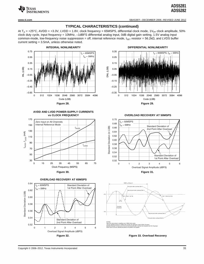
064
062
060
058
056
054
052
Sta
ndard
Devia
tion (
LS
B)
0 1 2 3 4 5 6
Overload Signal Amplitude (dBFS)
f = 65MSPS
f = 5MHzS
IN
Standard Deviation of
2nd Point After Overload
Standard Deviation of
1st Point After Overload
tS
16384 t (Group 1)S
Set 1 Point 1 (of 16) Set 1 Point 2 (of 16)
First point after overload (Set 1)
First point after overload (Set 2)
Second point after overload (Set 2)
Second point after overload (Set 1)
Overload
Amplitude
NOTES
Input sine wave phase is repetitive over 16384 clock cycles
16 such repetitive groups (of 16384 clock cycles) are capturedndasha total of 262144 points
Standard deviation of every set of are analyzed over the 16 groups
Worst case of all such standard deviations are plotted in the graphs
first and second points after overload
+FS
-FS
070
068
066
064
062
060
058
056
054
052
050
Sta
nd
ard
De
via
tio
n (
in L
SB
)
0 1 2 3 4 5 6
Overload Signal Amplitude (dBFS)
f = 50MSPS
f = 5MHzS
IN Standard Deviation of
2nd Point After Overload
Standard Deviation of
1st Point After Overload
170
130
110
90
70
30
Clock Frequency (MSPS)
5 75
I I
(mA
)A
VD
DLV
DD
352515 45
ILVDD
IAVDD
Zero Input on All Channels
Internal Reference Mode150
55
50
65
075
055
035
015
-005
-025
-065
Code (LSB)
0 4096
INL
(LS
B)
30722048 25601536 35841024512
-045
f = 65MSPS
f = 5MHzS
IN
035
025
015
005
-005
-015
-035
Code (LSB)
0 4096
DN
L (
LS
B)
30722048 25601536 35841024512
-025
f = 65MSPS f = 5MHzS IN
ADS5281ADS5282
wwwticom SBAS397I ndashDECEMBER 2006ndashREVISED JUNE 2012
TYPICAL CHARACTERISTICS (continued)At TA = +25degC AVDD = +33V LVDD = 18V clock frequency = 65MSPS differential clock mode 1VPP clock amplitude 50clock duty cycle input frequency = 10MHz ndash1dBFS differential analog input 0dB digital gain setting 15V analog inputcommon-mode low-frequency noise suppression = off internal reference mode ISET resistor = 562kΩ and LVDS buffercurrent setting = 35mA unless otherwise noted
INTEGRAL NONLINEARITY DIFFERENTIAL NONLINEARITY
Figure 28 Figure 29
AVDD AND LVDD POWER-SUPPLY CURRENTSvs CLOCK FREQUENCY OVERLOAD RECOVERY AT 50MSPS
Figure 30 Figure 31
OVERLOAD RECOVERY AT 65MSPS
Figure 32 Figure 33 Overload Recovery
Copyright copy 2006ndash2012 Texas Instruments Incorporated 31
ADS5281ADS5282
SBAS397I ndashDECEMBER 2006ndashREVISED JUNE 2012 wwwticom
APPLICATION INFORMATION
The ADC output goes to a serializer that operatesTHEORY OF OPERATION from a 12x clock generated by the PLL The 12 databits from each channel are serialized and sent LSBThe ADS528x devices are a family of 8-channelfirst In addition to serializing the data the serializerhigh-speed CMOS ADCs The 12 bits given out byalso generates a 1x clock and a 6x clock Theseeach channel are serialized and sent out on a singleclocks are generated in the same way the serializedpair of pins in LVDS format All eight channels of thedata are generated so these clocks maintain perfectADS528x operate from a single clock (ADCLK) Thesynchronization with the data The data and clocksampling clocks for each of the eight channels areoutputs of the serializer are buffered externally usinggenerated from the input clock using a carefullyLVDS buffers Using LVDS buffers to transmit datamatched clock buffer tree The 12x clock required forexternally has multiple advantages such as athe serializer is generated internally from ADCLKreduced number of output pins (saving routing spaceusing a phase-locked loop (PLL) A 6x and a 1x clockon the board) reduced power consumption andare also output in LVDS format along with the datareduced effects of digital noise coupling to the analogto enable easy data capture The ADS528x operatescircuit inside the ADS528xfrom internally-generated reference voltages that are
trimmed to improve to a high level of accuracy The ADS528x operates from two sets of supplies andTrimmed references improve the gain matching grounds The analog supply and ground set isacross devices and provide the option to operate the identified as AVDD and AVSS while the digital set isdevices without having to externally drive and route identified by LVDD and LVSSreference lines The nominal values of REFT andREFB are 25V and 05V respectively The ANALOG INPUTreferences are internally scaled down differentially bya factor of 2 This scaling results in a differential input The analog input consists of a switched-capacitorof ndash1V to correspond to the zero code of the ADC based differential sample-and-hold architecture Thisand a differential input of +1V to correspond to the differential topology results in very good acfull-scale code (4095 LSB) VCM (the common-mode performance even for high input frequencies at highvoltage of REFT and REFB) is also made available sampling rates The INN and INP pins must beexternally through a pin and is nominally 15V externally biased around a common-mode voltage of
15V available on VCM For a full-scale differentialThe ADC employs a pipelined converter architectureinput each input pin (INN and INP) must swingthat consists of a combination of multi-bit and single-symmetrically between VCM + 05V and VCM ndash 05Vbit internal stages Each stage feeds its data into theresulting in a 2VPP differential input swing Thedigital error correction logic ensuring excellentmaximum input peak-to-peak differential swing isdifferential linearity and no missing codes at the 12-determined to be the difference between the internalbit levelreference voltages REFT (25V nominal) and REFB(05V nominal) Figure 34 illustrates the model of theinput driving circuit
32 Copyright copy 2006ndash2012 Texas Instruments Incorporated
CM Buffer
Internal
Voltage
Reference
Input
Circuitry
INP
INN
VCM
12kW
12kW
ADS528x
(2mA) facute S
50MSPS
5nH to 9nH (TQFP-80)
2nH to 3nH (QFN-64)
15pF
to 24pF
IN OUT
INP
15pF to
25pF
1W
1000W
to 1440W
5W
to 10W
1000W
to 1440W
5nH to 9nH (TQFP-80)
2nH to 3nH (QFN-64)
INN
15pF to
25pF
1W
15W
to 25W
15W
to 30W
02pF
to 03pF
IN OUT
15pF
to 24pF
IN OUT
5W
to 10W
15W
to 25W
15W
to 30W
IN OUT
IN
OUT
16 to 32W W
IN OUT
IN OUT
OUTP
OUTN
Switches that are ON
in SAMPLE phase
Switches that are ON
in HOLD phase
ADS5281ADS5282
wwwticom SBAS397I ndashDECEMBER 2006ndashREVISED JUNE 2012
Figure 34 Analog Input Circuit Model
during ac-coupling by increasing VCM by roughlyInput Common-Mode Current 75mV When operating above 50MSPS it is
recommended that additional parallel resistors beThe input stage of all eight ADCs together sinks aadded externally to restore the input common-modecommon-mode current on the order of 2mA atto at least 14V if the inputs are to be ac-coupled50MSPS Equation 3 describes the dependency of
the common-mode current and the samplingfrequency
(3)
If the driving stage is dc-coupled to the inputs thenEquation 3 can be used to determine its common-mode drive capability and impedance The inputs canalso be ac-coupled to the INN and INP pins In thatcase the input common-mode is set by two internal12kΩ resistors connecting the input pins to VCM Thisarchitecture is shown in Figure 35
When the inputs are ac-coupled there is a drop inthe voltages at INP and INN relative to VCM This can Dashed area denotes one of eight channelsbe computed from Equation 3 At 50MSPS for
Figure 35 Common-Mode Biasing of Input Pinsexample the drop at each of the 16 input pins is150mV which is not optimal for ADC operationInitialization Registers 1 and 5 described in theInitialization Registers table can be used to partiallyreduce the effect of this input common-mode drop
Copyright copy 2006ndash2012 Texas Instruments Incorporated 33
01 Fm 50W
50W
200W
200W
INP
VCM
INN
01 Fm
12 21
47W
47W
01 Fm
01 Fm
25W
25W
11
INP
VCM
INN
ADS5281ADS5282
SBAS397I ndashDECEMBER 2006ndashREVISED JUNE 2012 wwwticom
Driving Circuit At high input frequencies the mismatch in thetransformer parasitic capacitance (between theFor optimum performance the analog inputs must bewindings) results in degraded even-order harmonicdriven differentially This approach improves theperformance Connecting two identical RFcommon-mode noise immunity and even-ordertransformers back-to-back helps to minimize thisharmonic rejection Input configurations using RFmismatch and good performance is obtained fortransformers suitable for low and high inputhigh-frequency input signals An additionalfrequencies are shown in Figure 36 and Figure 37termination resistor pair is required between the tworespectively The single-ended signal is fed to thetransformers as shown in Figure 37 The center pointprimary winding of the RF transformer Theof this termination is connected to ground to improvetransformer is terminated by 50Ω resistor on thethe balance between the positive and negative sidessecondary side Placing the termination on theThe values of the terminations between thesecondary side helps to shield the kicks caused bytransformers and on the secondary side must bethe input sampling capacitors from the RFchosen to achieve an overall 50Ω (in the case of 50Ωtransformer leakage inductances The termination issource impedance)accomplished by two 25Ω resistors connected in
series with the center point connected to the 15Vcommon-mode The 47Ω resistor in series with eachinput pin is required to damp the ringing caused bythe device package parasitics
Figure 36 Drive Circuit at Low Input Frequencies
Figure 37 Drive Circuit at High Input Frequencies
34 Copyright copy 2006ndash2012 Texas Instruments Incorporated
CLKP
CLKN
CMOS Clock Input
01 Fm
01 Fm
CLKP
CLKN
CMOS Single-Ended
Clock
0V
CLKP
CLKN
Differential Sine-Wave
PECL or LVDS Clock Input
01 Fm
01 Fm
5kW 5kW
VCM
CLKP
CLKN
VCM
ADS5281ADS5282
wwwticom SBAS397I ndashDECEMBER 2006ndashREVISED JUNE 2012
CLOCK INPUT
The eight channels on the device operate from asingle ADCLK input To ensure that the aperturedelay and jitter are the same for all channels a clocktree network is used to generate individual samplingclocks to each channel The clock paths for all thechannels are matched from the source point to thesampling circuit This architecture ensures that theperformance and timing for all channels are identicalThe use of the clock tree for matching introduces anaperture delay that is defined as the delay betweenthe rising edge of ADCLK and the actual instant ofsampling The aperture delays for all the channelsare matched to the best possible extent A mismatchof plusmn20ps (plusmn3σ) could exist between the apertureinstants of the eight ADCs within the same chip Figure 39 Internal Clock BufferHowever the aperture delays of ADCs across twodifferent chips can be several hundred picosecondsapart
The ADS528x can be made to operate either inCMOS single-ended clock mode (default isDIFF_CLK = 0) or differential clock mode (SINELVPECL or LVDS) When operating in the single-ended clock mode CLKN must be forced to 0VDCand the single-ended CMOS applied on the CLKP pinThis operation is shown in Figure 38
Figure 40 Differential Clock Driving Circuit(DIFF_CLK = 1)
Figure 38 Single-Ended Clock Driving Circuit(DIFF_CLK = 0)
When configured to operate in the differential clock Figure 41 Single-Ended Clock Driving Circuitmode (register bit DIFF_CLK = 1) the ADS528x clock When DIFF_CLK = 1inputs can be driven differentially (SINE LVPECL orLVDS) with little or no difference in performance
For best performance the clock inputs must bebetween them or with a single-ended (LVCMOS)driven differentially in order to reduce susceptibility toThe common-mode voltage of the clock inputs is setcommon-mode noise For high input frequencyto VCM using internal 5kΩ resistors as shown insampling it is recommended to use a clock sourceFigure 39 This method allows using transformer-with very low jitter Bandpass filtering of the clockcoupled drive circuits for a sine wave clock or ac-source can help reduce the effect of jitter If the dutycoupling for LVPECL and LVDS clock sources ascycle deviates from 50 by more than 2 or 3 it isshown in Figure 40 When operating in the differentialrecommended to enable the DCC through register bitclock mode the single-ended CMOS clock can be ac-EN_DCCcoupled to the CLKP input with CLKN (pin 11)
connected to ground with a 01μF capacitor asshown in Figure 41
Copyright copy 2006ndash2012 Texas Instruments Incorporated 35
Threshold 1 Threshold 2 Threshold 3
10 MHz 45 MHz 65 MHz
Sampling Frequency
ADS5281ADS5282
SBAS397I ndashDECEMBER 2006ndashREVISED JUNE 2012 wwwticom
PLL OPERATION ACROSS SAMPLING Step 2 Disable the PLL automatic switch and setFREQUENCY the PLL configuration depending on the clock
frequencyThe ADS528X uses a PLL for generating the highspeed bit clock (LCLK) the frame clock (ADCLK) amp SAMPLE CLOCK FREQUENCY REGISTER SETTING (Hex)internal clocks for the serializer operation RANGE (MSPS)
Min Max Address DataTo enable operation across the entire frequencyrange the PLL is automatically configured to one of 10 25 E3 0060four states depending on the sampling clock 15 45 E3 00A0frequency range The frequency range detection isautomatic and each time the sampling frequency With the above settings applied for the respectivecrosses a threshold the PLL changes its frequency ranges the part will continue toconfiguration to a new state To prevent unwanted operate as per the stated datasheet specificationstoggling of PLL state around a threshold the circuit for all timing parameters at all specifiedhas an inbuilt hysteresis The ADS528x has three frequencies EXCEPT for the timing specificationsthresholds ndash taking into account the hysteresis range at 40MSPS At 40MSPS the affected parametersof each threshold variation across devices and are ndash Data setup time Data hold time and Clocktemperature the thresholds can span the sampling propagation delay (refer to LVDS Timing )clock frequency range from 10MHz to 45MHz 2 For sampling clock frequency ge 45MSPS
As there are no PLL thresholds beyond 45MHzno change in PLL configuration can occur as thetemperature in the system stabilizes TheADS528x can be used in the system withoutusing the above software fix
INPUT OVER-VOLTAGE RECOVERY
The differential peak-to-peak full-scale rangesupported by the ADS528x is nominally 20V TheADS528x is specially designed to handle an over-
Figure 42 Variation of Thresholds Across voltage condition where the differential peak-to-peakSampling Frequency voltage can be up to twice the ADC full-scale range
If the input common-mode is not considerably offfrom VCM during overload (less than 300mV aroundBased on actual system clock frequency there arethe nominal value of 15V) recovery from an over-two scenariosvoltage pulse input of twice the amplitude of a full-1 For sampling clock frequency lt 45MSPSscale pulse is expected to be within one clock cycle
After system power up depending on the when the input switches from overload to zero signalfrequency of operation and the frequencythreshold for the given device the frequency REFERENCE CIRCUITrange detection circuit may change state once In
The digital beam-forming algorithm in an ultrasoundsome applications where a timing calibrationsystem relies on gain matching across all receivermight be done at the system level once afterchannels A typical system would have about 12 octalpower up this subsequent change of the PLLADCs on the board In such a case it is critical tostate might be undesirable as it can cause a lossensure that the gain is matched essentially requiringof alignment in the received data A software fixthe reference voltages seen by all the ADCs to be thefor eliminating this one-time change of PLL statesame Matching references within the eight channelsexists using the serial register interfaceof a chip is done by using a single internal referencendash Disable the automatic switch of the PLLvoltage buffer Trimming the reference voltages onconfiguration based on frequency detectedeach chip during production ensures that thendash In addition to disabling the switching it is alsoreference voltages are well-matched across differentrequired to set the PLL to the correctchipsconfiguration depending on the sample clock
frequency used in the system All bias currents required for the internal operation ofthe device are set using an external resistor toThe following sequence of register writes must beground at the ISET pin Using a 562kΩ resistor on ISETfollowedgenerates an internal reference current of 20μA This
Step 1 Write Address = 0x01 Data = 0x0010 current is mirrored internally to generate the biascurrent for the internal blocks Using a larger external
36 Copyright copy 2006ndash2012 Texas Instruments Incorporated
VREF = 15V -B
VCM
15V
VREF = 15V +T
VCM
15V
REFT
REFB
ISET
01 Fm 22 Fm
0 to
2
W
W
0 toW
2W
562kW
22 Fm 01 Fm
ADS528x
ADS5281ADS5282
wwwticom SBAS397I ndashDECEMBER 2006ndashREVISED JUNE 2012
resistor at ISET reduces the reference bias current and The device also supports the use of externalthereby scales down the device operating power reference voltages There are two methods to forceHowever it is recommended that the external resistor the references externally The first method involvesbe within 10 of the specified value of 562kΩ so pulling INTEXT low and forcing externally REFT andthat the internal bias margins for the various blocks REFB to 25V and 05V nominally respectively In thisare proper mode the internal reference buffer goes to a 3-state
output The external reference driving circuit shouldBuffering the internal bandgap voltage also generates be designed to provide the required switching currentthe common-mode voltage VCM which is set to the for the eight ADCs inside the chip It should be notedmidlevel of REFT and REFB and is accessible on a that in this mode VCM and ISET continue to bepin (pin 65 in TQFP-80 package pin 53 in QFN-64 generated from the internal bandgap voltage as inpackage) It is meant as a reference voltage to derive the internal reference mode It is therefore importantthe input common-mode if the input is directly to ensure that the common-mode voltage of thecoupled It can also be used to derive the reference externally-forced reference voltages matches tocommon-mode voltage in the external reference within 50mV of VCMmode The suggested decoupling for the referencepins is shown in Figure 43 The second method of forcing the reference voltages
externally can be accessed by pulling INTEXT lowand programming the serial interface to drive theexternal reference mode through the VCM pin (registerbit called EXT_REF_VCM) In this mode VCMbecomes configured as an input pin that can bedriven from external circuitry The internal referencebuffers driving REFT and REFB are active in thismode Forcing 15V on the VCM pin in the moderesults in REFT and REFB coming to 25V and 05Vrespectively In general the voltages on REFT andREFB in this mode are given by Equation 4 andEquation 5 respectively
(4)Figure 43 Suggested Decoupling on the
Reference Pins(5)
The state of the reference voltage internal buffersduring various combinations of the PD INTEXT andEXT_REF_VCM register bits is described in Table 8
Table 8 State of Reference Voltages for Various Combinations of PD INTEXT and EXT_REF_VCM
REGISTER BIT INTERNAL BUFFER STATE
PD 0 0 1 1 0 0 1 1
INTEXT 0 1 0 1 0 1 0 1
EXT_REF_VCM 0 0 0 0 1 1 1 1
REFT buffer 3-state 25V 3-state 25V (1) 15V + VCM15V Do not use 25V (1) Do not use
REFB buffer 3-state 05V 3-state 05V (1) 15V ndash VCM15V Do not use 05V (1) Do not use
VCM pin 15V 15V 15V 15V Force Do not use Force Do not use
(1) Weakly forced with reduced strengthsections while LVDD and LVSS are used to denotethe digital supplies Care is taken to ensure that thereNOISE COUPLING ISSUESis minimal interaction between the supply sets within
High-speed mixed signals are sensitive to various the device The extent of noise coupled andtypes of noise coupling One primary source of noise transmitted from the digital to the analog sectionsis the switching noise from the serializer and the depends onoutput buffers Maximum care is taken to isolate
1 The effective inductances of each of the supplythese noise sources from the sensitive analog blocksand ground setsAs a starting point the analog and digital domains of
2 The isolation between the digital and analogthe device are clearly demarcated AVDD and AVSSsupply and ground setsare used to denote the supplies for the analog
Copyright copy 2006ndash2012 Texas Instruments Incorporated 37
ADS5281ADS5282
SBAS397I ndashDECEMBER 2006ndashREVISED JUNE 2012 wwwticom
Smaller effective inductance of the supply and ground It is recommended that the isolation be maintained onpins leads to better noise suppression For this the board by using separate supplies to drive AVDDreason multiple pins are used to drive each supply and LVDD as well as separate ground planes forand ground It is also critical to ensure that the AVSS and LVSS The use of LVDS buffers reducesimpedances of the supply and ground lines on the the injected noise considerably compared to CMOSboard are kept to the minimum possible values Use buffers The current in the LVDS buffer isof ground planes in the printed circuit board (PCB) as independent of the direction of switching Also thewell as large decoupling capacitors between the low output swing as well as the differential nature ofsupply and ground lines are necessary to obtain the the LVDS buffer results in low-noise couplingbest possible SNR performance from the device
38 Copyright copy 2006ndash2012 Texas Instruments Incorporated
ADS5281ADS5282
wwwticom SBAS397I ndashDECEMBER 2006ndashREVISED JUNE 2012
REVISION HISTORY
Changes from Revision G (March 2008) to Revision H Page
bull Changed second table and conditions in the Initialization Registers section 3
bull Changed In Input Common-Mode Current section changed initialization register 5 to initialization registers 1 and 5to reflect change in Initialization Registers table 33
Changes from Revision F (March 2008) to Revision G Page
bull Deleted note (3) of Ordering Information table to indicate device status is now Production Data for all parts 2
bull Added new note (3) of Ordering Information table to indicate the quantity of transport media is available in thePackage Option Addendum 2
bull Added note (1) to Initialization Registers section to indicate it is no longer necessary to program initializationregisters 1 to 4 3
bull Changed maximum specifications for ADS5282 column in the Power SupplymdashInternal Reference Mode section ofElectrical Characteristics (By Device) table 6
bull Changed minimum specification for ADS5282 column in the f = 10 MHz row of the SNR section of ElectricalCharacteristics (By Device) table 6
Changes from Revision H (March 2008) to Revision I Page
bull Added table in the INITIALIZATION REGISTERS section 3
bull Added table in the LVDS OUTPUT TIMING CHARACTERISTICS section 14
bull Added PLL OPERATION ACROSS SAMPLING FREQUENCY section 36
Copyright copy 2006ndash2012 Texas Instruments Incorporated 39
PACKAGE OPTION ADDENDUM
wwwticom 26-Oct-2016
Addendum-Page 1
PACKAGING INFORMATION
Orderable Device Status(1)
Package Type PackageDrawing
Pins PackageQty
Eco Plan(2)
LeadBall Finish(6)
MSL Peak Temp(3)
Op Temp (degC) Device Marking(45)
Samples
ADS5281IPFP ACTIVE HTQFP PFP 80 96 Green (RoHSamp no SbBr)
CU NIPDAU Level-3-260C-168 HR -40 to 85 ADS5281I
ADS5281IPFPR ACTIVE HTQFP PFP 80 1000 Green (RoHSamp no SbBr)
CU NIPDAU Level-3-260C-168 HR -40 to 85 ADS5281I
ADS5281IRGCR ACTIVE VQFN RGC 64 2000 Green (RoHSamp no SbBr)
CU NIPDAU Level-3-260C-168 HR -40 to 85 AZ5281
ADS5281IRGCT ACTIVE VQFN RGC 64 250 Green (RoHSamp no SbBr)
CU NIPDAU Level-3-260C-168 HR -40 to 85 AZ5281
ADS5282IRGCR ACTIVE VQFN RGC 64 2000 Green (RoHSamp no SbBr)
CU NIPDAU Level-3-260C-168 HR -40 to 85 AZ5282
ADS5282IRGCT ACTIVE VQFN RGC 64 250 Green (RoHSamp no SbBr)
CU NIPDAU Level-3-260C-168 HR -40 to 85 AZ5282
(1) The marketing status values are defined as followsACTIVE Product device recommended for new designsLIFEBUY TI has announced that the device will be discontinued and a lifetime-buy period is in effectNRND Not recommended for new designs Device is in production to support existing customers but TI does not recommend using this part in a new designPREVIEW Device has been announced but is not in production Samples may or may not be availableOBSOLETE TI has discontinued the production of the device
(2) Eco Plan - The planned eco-friendly classification Pb-Free (RoHS) Pb-Free (RoHS Exempt) or Green (RoHS amp no SbBr) - please check httpwwwticomproductcontent for the latest availabilityinformation and additional product content detailsTBD The Pb-FreeGreen conversion plan has not been definedPb-Free (RoHS) TIs terms Lead-Free or Pb-Free mean semiconductor products that are compatible with the current RoHS requirements for all 6 substances including the requirement thatlead not exceed 01 by weight in homogeneous materials Where designed to be soldered at high temperatures TI Pb-Free products are suitable for use in specified lead-free processesPb-Free (RoHS Exempt) This component has a RoHS exemption for either 1) lead-based flip-chip solder bumps used between the die and package or 2) lead-based die adhesive used betweenthe die and leadframe The component is otherwise considered Pb-Free (RoHS compatible) as defined aboveGreen (RoHS amp no SbBr) TI defines Green to mean Pb-Free (RoHS compatible) and free of Bromine (Br) and Antimony (Sb) based flame retardants (Br or Sb do not exceed 01 by weightin homogeneous material)
(3) MSL Peak Temp - The Moisture Sensitivity Level rating according to the JEDEC industry standard classifications and peak solder temperature
(4) There may be additional marking which relates to the logo the lot trace code information or the environmental category on the device
(5) Multiple Device Markings will be inside parentheses Only one Device Marking contained in parentheses and separated by a ~ will appear on a device If a line is indented then it is a continuationof the previous line and the two combined represent the entire Device Marking for that device
PACKAGE OPTION ADDENDUM
wwwticom 26-Oct-2016
Addendum-Page 2
(6) LeadBall Finish - Orderable Devices may have multiple material finish options Finish options are separated by a vertical ruled line LeadBall Finish values may wrap to two lines if the finishvalue exceeds the maximum column width
Important Information and DisclaimerThe information provided on this page represents TIs knowledge and belief as of the date that it is provided TI bases its knowledge and belief on informationprovided by third parties and makes no representation or warranty as to the accuracy of such information Efforts are underway to better integrate information from third parties TI has taken andcontinues to take reasonable steps to provide representative and accurate information but may not have conducted destructive testing or chemical analysis on incoming materials and chemicalsTI and TI suppliers consider certain information to be proprietary and thus CAS numbers and other limited information may not be available for release
In no event shall TIs liability arising out of such information exceed the total purchase price of the TI part(s) at issue in this document sold by TI to Customer on an annual basis
TAPE AND REEL INFORMATION
All dimensions are nominal
Device PackageType
PackageDrawing
Pins SPQ ReelDiameter
(mm)
ReelWidth
W1 (mm)
A0(mm)
B0(mm)
K0(mm)
P1(mm)
W(mm)
Pin1Quadrant
ADS5281IPFPR HTQFP PFP 80 1000 3300 244 150 150 15 200 240 Q2
ADS5281IRGCR VQFN RGC 64 2000 3300 164 93 93 15 120 160 Q2
ADS5281IRGCT VQFN RGC 64 250 1800 164 93 93 15 120 160 Q2
ADS5282IRGCR VQFN RGC 64 2000 3300 164 93 93 15 120 160 Q2
ADS5282IRGCT VQFN RGC 64 250 1800 164 93 93 15 120 160 Q2
PACKAGE MATERIALS INFORMATION
wwwticom 14-May-2015
Pack Materials-Page 1
All dimensions are nominal
Device Package Type Package Drawing Pins SPQ Length (mm) Width (mm) Height (mm)
ADS5281IPFPR HTQFP PFP 80 1000 3670 3670 450
ADS5281IRGCR VQFN RGC 64 2000 3366 3366 286
ADS5281IRGCT VQFN RGC 64 250 2130 1910 550
ADS5282IRGCR VQFN RGC 64 2000 3366 3366 286
ADS5282IRGCT VQFN RGC 64 250 2130 1910 550
PACKAGE MATERIALS INFORMATION
wwwticom 14-May-2015
Pack Materials-Page 2
wwwticom
IMPORTANT NOTICE
Texas Instruments Incorporated and its subsidiaries (TI) reserve the right to make corrections enhancements improvements and otherchanges to its semiconductor products and services per JESD46 latest issue and to discontinue any product or service per JESD48 latestissue Buyers should obtain the latest relevant information before placing orders and should verify that such information is current andcomplete All semiconductor products (also referred to herein as ldquocomponentsrdquo) are sold subject to TIrsquos terms and conditions of salesupplied at the time of order acknowledgmentTI warrants performance of its components to the specifications applicable at the time of sale in accordance with the warranty in TIrsquos termsand conditions of sale of semiconductor products Testing and other quality control techniques are used to the extent TI deems necessaryto support this warranty Except where mandated by applicable law testing of all parameters of each component is not necessarilyperformedTI assumes no liability for applications assistance or the design of Buyersrsquo products Buyers are responsible for their products andapplications using TI components To minimize the risks associated with Buyersrsquo products and applications Buyers should provideadequate design and operating safeguardsTI does not warrant or represent that any license either express or implied is granted under any patent right copyright mask work right orother intellectual property right relating to any combination machine or process in which TI components or services are used Informationpublished by TI regarding third-party products or services does not constitute a license to use such products or services or a warranty orendorsement thereof Use of such information may require a license from a third party under the patents or other intellectual property of thethird party or a license from TI under the patents or other intellectual property of TIReproduction of significant portions of TI information in TI data books or data sheets is permissible only if reproduction is without alterationand is accompanied by all associated warranties conditions limitations and notices TI is not responsible or liable for such altereddocumentation Information of third parties may be subject to additional restrictionsResale of TI components or services with statements different from or beyond the parameters stated by TI for that component or servicevoids all express and any implied warranties for the associated TI component or service and is an unfair and deceptive business practiceTI is not responsible or liable for any such statementsBuyer acknowledges and agrees that it is solely responsible for compliance with all legal regulatory and safety-related requirementsconcerning its products and any use of TI components in its applications notwithstanding any applications-related information or supportthat may be provided by TI Buyer represents and agrees that it has all the necessary expertise to create and implement safeguards whichanticipate dangerous consequences of failures monitor failures and their consequences lessen the likelihood of failures that might causeharm and take appropriate remedial actions Buyer will fully indemnify TI and its representatives against any damages arising out of the useof any TI components in safety-critical applicationsIn some cases TI components may be promoted specifically to facilitate safety-related applications With such components TIrsquos goal is tohelp enable customers to design and create their own end-product solutions that meet applicable functional safety standards andrequirements Nonetheless such components are subject to these termsNo TI components are authorized for use in FDA Class III (or similar life-critical medical equipment) unless authorized officers of the partieshave executed a special agreement specifically governing such useOnly those TI components which TI has specifically designated as military grade or ldquoenhanced plasticrdquo are designed and intended for use inmilitaryaerospace applications or environments Buyer acknowledges and agrees that any military or aerospace use of TI componentswhich have not been so designated is solely at the Buyers risk and that Buyer is solely responsible for compliance with all legal andregulatory requirements in connection with such useTI has specifically designated certain components as meeting ISOTS16949 requirements mainly for automotive use In any case of use ofnon-designated products TI will not be responsible for any failure to meet ISOTS16949
Products ApplicationsAudio wwwticomaudio Automotive and Transportation wwwticomautomotiveAmplifiers amplifierticom Communications and Telecom wwwticomcommunicationsData Converters dataconverterticom Computers and Peripherals wwwticomcomputersDLPreg Products wwwdlpcom Consumer Electronics wwwticomconsumer-appsDSP dspticom Energy and Lighting wwwticomenergyClocks and Timers wwwticomclocks Industrial wwwticomindustrialInterface interfaceticom Medical wwwticommedicalLogic logicticom Security wwwticomsecurityPower Mgmt powerticom Space Avionics and Defense wwwticomspace-avionics-defenseMicrocontrollers microcontrollerticom Video and Imaging wwwticomvideoRFID wwwti-rfidcomOMAP Applications Processors wwwticomomap TI E2E Community e2eticomWireless Connectivity wwwticomwirelessconnectivity
Mailing Address Texas Instruments Post Office Box 655303 Dallas Texas 75265Copyright copy 2016 Texas Instruments Incorporated
- FEATURES
- APPLICATIONS
- DESCRIPTION
- ABSOLUTE MAXIMUM RATINGS
- RECOMMENDED OPERATING CONDITIONS
- INITIALIZATION REGISTERS
- DIGITAL CHARACTERISTICS
- ELECTRICAL CHARACTERISTICS
- ELECTRICAL CHARACTERISTICS (BY DEVICE)
- PIN CONFIGURATIONS
- FUNCTIONAL BLOCK DIAGRAM
- TIMING CHARACTERISTICS
- LVDS OUTPUT TIMING CHARACTERISTICS
- LVDS OUTPUT TIMING CHARACTERISTICS
- LVDS OUTPUT TIMING CHARACTERISTICS
- SERIAL INTERFACE
-
- Register Initialization
-
- SERIAL REGISTER MAP
- SUMMARY OF FEATURES
- DESCRIPTION OF SERIAL REGISTERS
-
- SOFTWARE RESET
- POWER-DOWN MODES
- LVDS DRIVE PROGRAMMABILITY
- LVDS INTERNAL TERMINATION PROGRAMMABILITY
- LOW-FREQUENCY NOISE SUPPRESSION MODE
- ANALOG INPUT INVERT
- LVDS TEST PATTERNS
- PROGRAMMABLE GAIN
- CLOCK REFERENCE AND DATA OUTPUT MODES
-
- INPUT CLOCK
- EXTERNAL REFERENCE
- BIT CLOCK PROGRAMMABILITY
- DATA OUTPUT FORMAT MODES
-
- TYPICAL CHARACTERISTICS
- APPLICATION INFORMATION
-
- THEORY OF OPERATION
- ANALOG INPUT
-
- Input Common-Mode Current
- Driving Circuit
-
- CLOCK INPUT
- PLL OPERATION ACROSS SAMPLING FREQUENCY
- INPUT OVER-VOLTAGE RECOVERY
- REFERENCE CIRCUIT
- NOISE COUPLING ISSUES
-
- Revision History
-

ADS5281ADS5282
SBAS397I ndashDECEMBER 2006ndashREVISED JUNE 2012 wwwticom
APPLICATION INFORMATION
The ADC output goes to a serializer that operatesTHEORY OF OPERATION from a 12x clock generated by the PLL The 12 databits from each channel are serialized and sent LSBThe ADS528x devices are a family of 8-channelfirst In addition to serializing the data the serializerhigh-speed CMOS ADCs The 12 bits given out byalso generates a 1x clock and a 6x clock Theseeach channel are serialized and sent out on a singleclocks are generated in the same way the serializedpair of pins in LVDS format All eight channels of thedata are generated so these clocks maintain perfectADS528x operate from a single clock (ADCLK) Thesynchronization with the data The data and clocksampling clocks for each of the eight channels areoutputs of the serializer are buffered externally usinggenerated from the input clock using a carefullyLVDS buffers Using LVDS buffers to transmit datamatched clock buffer tree The 12x clock required forexternally has multiple advantages such as athe serializer is generated internally from ADCLKreduced number of output pins (saving routing spaceusing a phase-locked loop (PLL) A 6x and a 1x clockon the board) reduced power consumption andare also output in LVDS format along with the datareduced effects of digital noise coupling to the analogto enable easy data capture The ADS528x operatescircuit inside the ADS528xfrom internally-generated reference voltages that are
trimmed to improve to a high level of accuracy The ADS528x operates from two sets of supplies andTrimmed references improve the gain matching grounds The analog supply and ground set isacross devices and provide the option to operate the identified as AVDD and AVSS while the digital set isdevices without having to externally drive and route identified by LVDD and LVSSreference lines The nominal values of REFT andREFB are 25V and 05V respectively The ANALOG INPUTreferences are internally scaled down differentially bya factor of 2 This scaling results in a differential input The analog input consists of a switched-capacitorof ndash1V to correspond to the zero code of the ADC based differential sample-and-hold architecture Thisand a differential input of +1V to correspond to the differential topology results in very good acfull-scale code (4095 LSB) VCM (the common-mode performance even for high input frequencies at highvoltage of REFT and REFB) is also made available sampling rates The INN and INP pins must beexternally through a pin and is nominally 15V externally biased around a common-mode voltage of
15V available on VCM For a full-scale differentialThe ADC employs a pipelined converter architectureinput each input pin (INN and INP) must swingthat consists of a combination of multi-bit and single-symmetrically between VCM + 05V and VCM ndash 05Vbit internal stages Each stage feeds its data into theresulting in a 2VPP differential input swing Thedigital error correction logic ensuring excellentmaximum input peak-to-peak differential swing isdifferential linearity and no missing codes at the 12-determined to be the difference between the internalbit levelreference voltages REFT (25V nominal) and REFB(05V nominal) Figure 34 illustrates the model of theinput driving circuit
32 Copyright copy 2006ndash2012 Texas Instruments Incorporated
CM Buffer
Internal
Voltage
Reference
Input
Circuitry
INP
INN
VCM
12kW
12kW
ADS528x
(2mA) facute S
50MSPS
5nH to 9nH (TQFP-80)
2nH to 3nH (QFN-64)
15pF
to 24pF
IN OUT
INP
15pF to
25pF
1W
1000W
to 1440W
5W
to 10W
1000W
to 1440W
5nH to 9nH (TQFP-80)
2nH to 3nH (QFN-64)
INN
15pF to
25pF
1W
15W
to 25W
15W
to 30W
02pF
to 03pF
IN OUT
15pF
to 24pF
IN OUT
5W
to 10W
15W
to 25W
15W
to 30W
IN OUT
IN
OUT
16 to 32W W
IN OUT
IN OUT
OUTP
OUTN
Switches that are ON
in SAMPLE phase
Switches that are ON
in HOLD phase
ADS5281ADS5282
wwwticom SBAS397I ndashDECEMBER 2006ndashREVISED JUNE 2012
Figure 34 Analog Input Circuit Model
during ac-coupling by increasing VCM by roughlyInput Common-Mode Current 75mV When operating above 50MSPS it is
recommended that additional parallel resistors beThe input stage of all eight ADCs together sinks aadded externally to restore the input common-modecommon-mode current on the order of 2mA atto at least 14V if the inputs are to be ac-coupled50MSPS Equation 3 describes the dependency of
the common-mode current and the samplingfrequency
(3)
If the driving stage is dc-coupled to the inputs thenEquation 3 can be used to determine its common-mode drive capability and impedance The inputs canalso be ac-coupled to the INN and INP pins In thatcase the input common-mode is set by two internal12kΩ resistors connecting the input pins to VCM Thisarchitecture is shown in Figure 35
When the inputs are ac-coupled there is a drop inthe voltages at INP and INN relative to VCM This can Dashed area denotes one of eight channelsbe computed from Equation 3 At 50MSPS for
Figure 35 Common-Mode Biasing of Input Pinsexample the drop at each of the 16 input pins is150mV which is not optimal for ADC operationInitialization Registers 1 and 5 described in theInitialization Registers table can be used to partiallyreduce the effect of this input common-mode drop
Copyright copy 2006ndash2012 Texas Instruments Incorporated 33
01 Fm 50W
50W
200W
200W
INP
VCM
INN
01 Fm
12 21
47W
47W
01 Fm
01 Fm
25W
25W
11
INP
VCM
INN
ADS5281ADS5282
SBAS397I ndashDECEMBER 2006ndashREVISED JUNE 2012 wwwticom
Driving Circuit At high input frequencies the mismatch in thetransformer parasitic capacitance (between theFor optimum performance the analog inputs must bewindings) results in degraded even-order harmonicdriven differentially This approach improves theperformance Connecting two identical RFcommon-mode noise immunity and even-ordertransformers back-to-back helps to minimize thisharmonic rejection Input configurations using RFmismatch and good performance is obtained fortransformers suitable for low and high inputhigh-frequency input signals An additionalfrequencies are shown in Figure 36 and Figure 37termination resistor pair is required between the tworespectively The single-ended signal is fed to thetransformers as shown in Figure 37 The center pointprimary winding of the RF transformer Theof this termination is connected to ground to improvetransformer is terminated by 50Ω resistor on thethe balance between the positive and negative sidessecondary side Placing the termination on theThe values of the terminations between thesecondary side helps to shield the kicks caused bytransformers and on the secondary side must bethe input sampling capacitors from the RFchosen to achieve an overall 50Ω (in the case of 50Ωtransformer leakage inductances The termination issource impedance)accomplished by two 25Ω resistors connected in
series with the center point connected to the 15Vcommon-mode The 47Ω resistor in series with eachinput pin is required to damp the ringing caused bythe device package parasitics
Figure 36 Drive Circuit at Low Input Frequencies
Figure 37 Drive Circuit at High Input Frequencies
34 Copyright copy 2006ndash2012 Texas Instruments Incorporated
CLKP
CLKN
CMOS Clock Input
01 Fm
01 Fm
CLKP
CLKN
CMOS Single-Ended
Clock
0V
CLKP
CLKN
Differential Sine-Wave
PECL or LVDS Clock Input
01 Fm
01 Fm
5kW 5kW
VCM
CLKP
CLKN
VCM
ADS5281ADS5282
wwwticom SBAS397I ndashDECEMBER 2006ndashREVISED JUNE 2012
CLOCK INPUT
The eight channels on the device operate from asingle ADCLK input To ensure that the aperturedelay and jitter are the same for all channels a clocktree network is used to generate individual samplingclocks to each channel The clock paths for all thechannels are matched from the source point to thesampling circuit This architecture ensures that theperformance and timing for all channels are identicalThe use of the clock tree for matching introduces anaperture delay that is defined as the delay betweenthe rising edge of ADCLK and the actual instant ofsampling The aperture delays for all the channelsare matched to the best possible extent A mismatchof plusmn20ps (plusmn3σ) could exist between the apertureinstants of the eight ADCs within the same chip Figure 39 Internal Clock BufferHowever the aperture delays of ADCs across twodifferent chips can be several hundred picosecondsapart
The ADS528x can be made to operate either inCMOS single-ended clock mode (default isDIFF_CLK = 0) or differential clock mode (SINELVPECL or LVDS) When operating in the single-ended clock mode CLKN must be forced to 0VDCand the single-ended CMOS applied on the CLKP pinThis operation is shown in Figure 38
Figure 40 Differential Clock Driving Circuit(DIFF_CLK = 1)
Figure 38 Single-Ended Clock Driving Circuit(DIFF_CLK = 0)
When configured to operate in the differential clock Figure 41 Single-Ended Clock Driving Circuitmode (register bit DIFF_CLK = 1) the ADS528x clock When DIFF_CLK = 1inputs can be driven differentially (SINE LVPECL orLVDS) with little or no difference in performance
For best performance the clock inputs must bebetween them or with a single-ended (LVCMOS)driven differentially in order to reduce susceptibility toThe common-mode voltage of the clock inputs is setcommon-mode noise For high input frequencyto VCM using internal 5kΩ resistors as shown insampling it is recommended to use a clock sourceFigure 39 This method allows using transformer-with very low jitter Bandpass filtering of the clockcoupled drive circuits for a sine wave clock or ac-source can help reduce the effect of jitter If the dutycoupling for LVPECL and LVDS clock sources ascycle deviates from 50 by more than 2 or 3 it isshown in Figure 40 When operating in the differentialrecommended to enable the DCC through register bitclock mode the single-ended CMOS clock can be ac-EN_DCCcoupled to the CLKP input with CLKN (pin 11)
connected to ground with a 01μF capacitor asshown in Figure 41
Copyright copy 2006ndash2012 Texas Instruments Incorporated 35
Threshold 1 Threshold 2 Threshold 3
10 MHz 45 MHz 65 MHz
Sampling Frequency
ADS5281ADS5282
SBAS397I ndashDECEMBER 2006ndashREVISED JUNE 2012 wwwticom
PLL OPERATION ACROSS SAMPLING Step 2 Disable the PLL automatic switch and setFREQUENCY the PLL configuration depending on the clock
frequencyThe ADS528X uses a PLL for generating the highspeed bit clock (LCLK) the frame clock (ADCLK) amp SAMPLE CLOCK FREQUENCY REGISTER SETTING (Hex)internal clocks for the serializer operation RANGE (MSPS)
Min Max Address DataTo enable operation across the entire frequencyrange the PLL is automatically configured to one of 10 25 E3 0060four states depending on the sampling clock 15 45 E3 00A0frequency range The frequency range detection isautomatic and each time the sampling frequency With the above settings applied for the respectivecrosses a threshold the PLL changes its frequency ranges the part will continue toconfiguration to a new state To prevent unwanted operate as per the stated datasheet specificationstoggling of PLL state around a threshold the circuit for all timing parameters at all specifiedhas an inbuilt hysteresis The ADS528x has three frequencies EXCEPT for the timing specificationsthresholds ndash taking into account the hysteresis range at 40MSPS At 40MSPS the affected parametersof each threshold variation across devices and are ndash Data setup time Data hold time and Clocktemperature the thresholds can span the sampling propagation delay (refer to LVDS Timing )clock frequency range from 10MHz to 45MHz 2 For sampling clock frequency ge 45MSPS
As there are no PLL thresholds beyond 45MHzno change in PLL configuration can occur as thetemperature in the system stabilizes TheADS528x can be used in the system withoutusing the above software fix
INPUT OVER-VOLTAGE RECOVERY
The differential peak-to-peak full-scale rangesupported by the ADS528x is nominally 20V TheADS528x is specially designed to handle an over-
Figure 42 Variation of Thresholds Across voltage condition where the differential peak-to-peakSampling Frequency voltage can be up to twice the ADC full-scale range
If the input common-mode is not considerably offfrom VCM during overload (less than 300mV aroundBased on actual system clock frequency there arethe nominal value of 15V) recovery from an over-two scenariosvoltage pulse input of twice the amplitude of a full-1 For sampling clock frequency lt 45MSPSscale pulse is expected to be within one clock cycle
After system power up depending on the when the input switches from overload to zero signalfrequency of operation and the frequencythreshold for the given device the frequency REFERENCE CIRCUITrange detection circuit may change state once In
The digital beam-forming algorithm in an ultrasoundsome applications where a timing calibrationsystem relies on gain matching across all receivermight be done at the system level once afterchannels A typical system would have about 12 octalpower up this subsequent change of the PLLADCs on the board In such a case it is critical tostate might be undesirable as it can cause a lossensure that the gain is matched essentially requiringof alignment in the received data A software fixthe reference voltages seen by all the ADCs to be thefor eliminating this one-time change of PLL statesame Matching references within the eight channelsexists using the serial register interfaceof a chip is done by using a single internal referencendash Disable the automatic switch of the PLLvoltage buffer Trimming the reference voltages onconfiguration based on frequency detectedeach chip during production ensures that thendash In addition to disabling the switching it is alsoreference voltages are well-matched across differentrequired to set the PLL to the correctchipsconfiguration depending on the sample clock
frequency used in the system All bias currents required for the internal operation ofthe device are set using an external resistor toThe following sequence of register writes must beground at the ISET pin Using a 562kΩ resistor on ISETfollowedgenerates an internal reference current of 20μA This
Step 1 Write Address = 0x01 Data = 0x0010 current is mirrored internally to generate the biascurrent for the internal blocks Using a larger external
36 Copyright copy 2006ndash2012 Texas Instruments Incorporated
VREF = 15V -B
VCM
15V
VREF = 15V +T
VCM
15V
REFT
REFB
ISET
01 Fm 22 Fm
0 to
2
W
W
0 toW
2W
562kW
22 Fm 01 Fm
ADS528x
ADS5281ADS5282
wwwticom SBAS397I ndashDECEMBER 2006ndashREVISED JUNE 2012
resistor at ISET reduces the reference bias current and The device also supports the use of externalthereby scales down the device operating power reference voltages There are two methods to forceHowever it is recommended that the external resistor the references externally The first method involvesbe within 10 of the specified value of 562kΩ so pulling INTEXT low and forcing externally REFT andthat the internal bias margins for the various blocks REFB to 25V and 05V nominally respectively In thisare proper mode the internal reference buffer goes to a 3-state
output The external reference driving circuit shouldBuffering the internal bandgap voltage also generates be designed to provide the required switching currentthe common-mode voltage VCM which is set to the for the eight ADCs inside the chip It should be notedmidlevel of REFT and REFB and is accessible on a that in this mode VCM and ISET continue to bepin (pin 65 in TQFP-80 package pin 53 in QFN-64 generated from the internal bandgap voltage as inpackage) It is meant as a reference voltage to derive the internal reference mode It is therefore importantthe input common-mode if the input is directly to ensure that the common-mode voltage of thecoupled It can also be used to derive the reference externally-forced reference voltages matches tocommon-mode voltage in the external reference within 50mV of VCMmode The suggested decoupling for the referencepins is shown in Figure 43 The second method of forcing the reference voltages
externally can be accessed by pulling INTEXT lowand programming the serial interface to drive theexternal reference mode through the VCM pin (registerbit called EXT_REF_VCM) In this mode VCMbecomes configured as an input pin that can bedriven from external circuitry The internal referencebuffers driving REFT and REFB are active in thismode Forcing 15V on the VCM pin in the moderesults in REFT and REFB coming to 25V and 05Vrespectively In general the voltages on REFT andREFB in this mode are given by Equation 4 andEquation 5 respectively
(4)Figure 43 Suggested Decoupling on the
Reference Pins(5)
The state of the reference voltage internal buffersduring various combinations of the PD INTEXT andEXT_REF_VCM register bits is described in Table 8
Table 8 State of Reference Voltages for Various Combinations of PD INTEXT and EXT_REF_VCM
REGISTER BIT INTERNAL BUFFER STATE
PD 0 0 1 1 0 0 1 1
INTEXT 0 1 0 1 0 1 0 1
EXT_REF_VCM 0 0 0 0 1 1 1 1
REFT buffer 3-state 25V 3-state 25V (1) 15V + VCM15V Do not use 25V (1) Do not use
REFB buffer 3-state 05V 3-state 05V (1) 15V ndash VCM15V Do not use 05V (1) Do not use
VCM pin 15V 15V 15V 15V Force Do not use Force Do not use
(1) Weakly forced with reduced strengthsections while LVDD and LVSS are used to denotethe digital supplies Care is taken to ensure that thereNOISE COUPLING ISSUESis minimal interaction between the supply sets within
High-speed mixed signals are sensitive to various the device The extent of noise coupled andtypes of noise coupling One primary source of noise transmitted from the digital to the analog sectionsis the switching noise from the serializer and the depends onoutput buffers Maximum care is taken to isolate
1 The effective inductances of each of the supplythese noise sources from the sensitive analog blocksand ground setsAs a starting point the analog and digital domains of
2 The isolation between the digital and analogthe device are clearly demarcated AVDD and AVSSsupply and ground setsare used to denote the supplies for the analog
Copyright copy 2006ndash2012 Texas Instruments Incorporated 37
ADS5281ADS5282
SBAS397I ndashDECEMBER 2006ndashREVISED JUNE 2012 wwwticom
Smaller effective inductance of the supply and ground It is recommended that the isolation be maintained onpins leads to better noise suppression For this the board by using separate supplies to drive AVDDreason multiple pins are used to drive each supply and LVDD as well as separate ground planes forand ground It is also critical to ensure that the AVSS and LVSS The use of LVDS buffers reducesimpedances of the supply and ground lines on the the injected noise considerably compared to CMOSboard are kept to the minimum possible values Use buffers The current in the LVDS buffer isof ground planes in the printed circuit board (PCB) as independent of the direction of switching Also thewell as large decoupling capacitors between the low output swing as well as the differential nature ofsupply and ground lines are necessary to obtain the the LVDS buffer results in low-noise couplingbest possible SNR performance from the device
38 Copyright copy 2006ndash2012 Texas Instruments Incorporated
ADS5281ADS5282
wwwticom SBAS397I ndashDECEMBER 2006ndashREVISED JUNE 2012
REVISION HISTORY
Changes from Revision G (March 2008) to Revision H Page
bull Changed second table and conditions in the Initialization Registers section 3
bull Changed In Input Common-Mode Current section changed initialization register 5 to initialization registers 1 and 5to reflect change in Initialization Registers table 33
Changes from Revision F (March 2008) to Revision G Page
bull Deleted note (3) of Ordering Information table to indicate device status is now Production Data for all parts 2
bull Added new note (3) of Ordering Information table to indicate the quantity of transport media is available in thePackage Option Addendum 2
bull Added note (1) to Initialization Registers section to indicate it is no longer necessary to program initializationregisters 1 to 4 3
bull Changed maximum specifications for ADS5282 column in the Power SupplymdashInternal Reference Mode section ofElectrical Characteristics (By Device) table 6
bull Changed minimum specification for ADS5282 column in the f = 10 MHz row of the SNR section of ElectricalCharacteristics (By Device) table 6
Changes from Revision H (March 2008) to Revision I Page
bull Added table in the INITIALIZATION REGISTERS section 3
bull Added table in the LVDS OUTPUT TIMING CHARACTERISTICS section 14
bull Added PLL OPERATION ACROSS SAMPLING FREQUENCY section 36
Copyright copy 2006ndash2012 Texas Instruments Incorporated 39
PACKAGE OPTION ADDENDUM
wwwticom 26-Oct-2016
Addendum-Page 1
PACKAGING INFORMATION
Orderable Device Status(1)
Package Type PackageDrawing
Pins PackageQty
Eco Plan(2)
LeadBall Finish(6)
MSL Peak Temp(3)
Op Temp (degC) Device Marking(45)
Samples
ADS5281IPFP ACTIVE HTQFP PFP 80 96 Green (RoHSamp no SbBr)
CU NIPDAU Level-3-260C-168 HR -40 to 85 ADS5281I
ADS5281IPFPR ACTIVE HTQFP PFP 80 1000 Green (RoHSamp no SbBr)
CU NIPDAU Level-3-260C-168 HR -40 to 85 ADS5281I
ADS5281IRGCR ACTIVE VQFN RGC 64 2000 Green (RoHSamp no SbBr)
CU NIPDAU Level-3-260C-168 HR -40 to 85 AZ5281
ADS5281IRGCT ACTIVE VQFN RGC 64 250 Green (RoHSamp no SbBr)
CU NIPDAU Level-3-260C-168 HR -40 to 85 AZ5281
ADS5282IRGCR ACTIVE VQFN RGC 64 2000 Green (RoHSamp no SbBr)
CU NIPDAU Level-3-260C-168 HR -40 to 85 AZ5282
ADS5282IRGCT ACTIVE VQFN RGC 64 250 Green (RoHSamp no SbBr)
CU NIPDAU Level-3-260C-168 HR -40 to 85 AZ5282
(1) The marketing status values are defined as followsACTIVE Product device recommended for new designsLIFEBUY TI has announced that the device will be discontinued and a lifetime-buy period is in effectNRND Not recommended for new designs Device is in production to support existing customers but TI does not recommend using this part in a new designPREVIEW Device has been announced but is not in production Samples may or may not be availableOBSOLETE TI has discontinued the production of the device
(2) Eco Plan - The planned eco-friendly classification Pb-Free (RoHS) Pb-Free (RoHS Exempt) or Green (RoHS amp no SbBr) - please check httpwwwticomproductcontent for the latest availabilityinformation and additional product content detailsTBD The Pb-FreeGreen conversion plan has not been definedPb-Free (RoHS) TIs terms Lead-Free or Pb-Free mean semiconductor products that are compatible with the current RoHS requirements for all 6 substances including the requirement thatlead not exceed 01 by weight in homogeneous materials Where designed to be soldered at high temperatures TI Pb-Free products are suitable for use in specified lead-free processesPb-Free (RoHS Exempt) This component has a RoHS exemption for either 1) lead-based flip-chip solder bumps used between the die and package or 2) lead-based die adhesive used betweenthe die and leadframe The component is otherwise considered Pb-Free (RoHS compatible) as defined aboveGreen (RoHS amp no SbBr) TI defines Green to mean Pb-Free (RoHS compatible) and free of Bromine (Br) and Antimony (Sb) based flame retardants (Br or Sb do not exceed 01 by weightin homogeneous material)
(3) MSL Peak Temp - The Moisture Sensitivity Level rating according to the JEDEC industry standard classifications and peak solder temperature
(4) There may be additional marking which relates to the logo the lot trace code information or the environmental category on the device
(5) Multiple Device Markings will be inside parentheses Only one Device Marking contained in parentheses and separated by a ~ will appear on a device If a line is indented then it is a continuationof the previous line and the two combined represent the entire Device Marking for that device
PACKAGE OPTION ADDENDUM
wwwticom 26-Oct-2016
Addendum-Page 2
(6) LeadBall Finish - Orderable Devices may have multiple material finish options Finish options are separated by a vertical ruled line LeadBall Finish values may wrap to two lines if the finishvalue exceeds the maximum column width
Important Information and DisclaimerThe information provided on this page represents TIs knowledge and belief as of the date that it is provided TI bases its knowledge and belief on informationprovided by third parties and makes no representation or warranty as to the accuracy of such information Efforts are underway to better integrate information from third parties TI has taken andcontinues to take reasonable steps to provide representative and accurate information but may not have conducted destructive testing or chemical analysis on incoming materials and chemicalsTI and TI suppliers consider certain information to be proprietary and thus CAS numbers and other limited information may not be available for release
In no event shall TIs liability arising out of such information exceed the total purchase price of the TI part(s) at issue in this document sold by TI to Customer on an annual basis
TAPE AND REEL INFORMATION
All dimensions are nominal
Device PackageType
PackageDrawing
Pins SPQ ReelDiameter
(mm)
ReelWidth
W1 (mm)
A0(mm)
B0(mm)
K0(mm)
P1(mm)
W(mm)
Pin1Quadrant
ADS5281IPFPR HTQFP PFP 80 1000 3300 244 150 150 15 200 240 Q2
ADS5281IRGCR VQFN RGC 64 2000 3300 164 93 93 15 120 160 Q2
ADS5281IRGCT VQFN RGC 64 250 1800 164 93 93 15 120 160 Q2
ADS5282IRGCR VQFN RGC 64 2000 3300 164 93 93 15 120 160 Q2
ADS5282IRGCT VQFN RGC 64 250 1800 164 93 93 15 120 160 Q2
PACKAGE MATERIALS INFORMATION
wwwticom 14-May-2015
Pack Materials-Page 1
All dimensions are nominal
Device Package Type Package Drawing Pins SPQ Length (mm) Width (mm) Height (mm)
ADS5281IPFPR HTQFP PFP 80 1000 3670 3670 450
ADS5281IRGCR VQFN RGC 64 2000 3366 3366 286
ADS5281IRGCT VQFN RGC 64 250 2130 1910 550
ADS5282IRGCR VQFN RGC 64 2000 3366 3366 286
ADS5282IRGCT VQFN RGC 64 250 2130 1910 550
PACKAGE MATERIALS INFORMATION
wwwticom 14-May-2015
Pack Materials-Page 2
wwwticom
IMPORTANT NOTICE
Texas Instruments Incorporated and its subsidiaries (TI) reserve the right to make corrections enhancements improvements and otherchanges to its semiconductor products and services per JESD46 latest issue and to discontinue any product or service per JESD48 latestissue Buyers should obtain the latest relevant information before placing orders and should verify that such information is current andcomplete All semiconductor products (also referred to herein as ldquocomponentsrdquo) are sold subject to TIrsquos terms and conditions of salesupplied at the time of order acknowledgmentTI warrants performance of its components to the specifications applicable at the time of sale in accordance with the warranty in TIrsquos termsand conditions of sale of semiconductor products Testing and other quality control techniques are used to the extent TI deems necessaryto support this warranty Except where mandated by applicable law testing of all parameters of each component is not necessarilyperformedTI assumes no liability for applications assistance or the design of Buyersrsquo products Buyers are responsible for their products andapplications using TI components To minimize the risks associated with Buyersrsquo products and applications Buyers should provideadequate design and operating safeguardsTI does not warrant or represent that any license either express or implied is granted under any patent right copyright mask work right orother intellectual property right relating to any combination machine or process in which TI components or services are used Informationpublished by TI regarding third-party products or services does not constitute a license to use such products or services or a warranty orendorsement thereof Use of such information may require a license from a third party under the patents or other intellectual property of thethird party or a license from TI under the patents or other intellectual property of TIReproduction of significant portions of TI information in TI data books or data sheets is permissible only if reproduction is without alterationand is accompanied by all associated warranties conditions limitations and notices TI is not responsible or liable for such altereddocumentation Information of third parties may be subject to additional restrictionsResale of TI components or services with statements different from or beyond the parameters stated by TI for that component or servicevoids all express and any implied warranties for the associated TI component or service and is an unfair and deceptive business practiceTI is not responsible or liable for any such statementsBuyer acknowledges and agrees that it is solely responsible for compliance with all legal regulatory and safety-related requirementsconcerning its products and any use of TI components in its applications notwithstanding any applications-related information or supportthat may be provided by TI Buyer represents and agrees that it has all the necessary expertise to create and implement safeguards whichanticipate dangerous consequences of failures monitor failures and their consequences lessen the likelihood of failures that might causeharm and take appropriate remedial actions Buyer will fully indemnify TI and its representatives against any damages arising out of the useof any TI components in safety-critical applicationsIn some cases TI components may be promoted specifically to facilitate safety-related applications With such components TIrsquos goal is tohelp enable customers to design and create their own end-product solutions that meet applicable functional safety standards andrequirements Nonetheless such components are subject to these termsNo TI components are authorized for use in FDA Class III (or similar life-critical medical equipment) unless authorized officers of the partieshave executed a special agreement specifically governing such useOnly those TI components which TI has specifically designated as military grade or ldquoenhanced plasticrdquo are designed and intended for use inmilitaryaerospace applications or environments Buyer acknowledges and agrees that any military or aerospace use of TI componentswhich have not been so designated is solely at the Buyers risk and that Buyer is solely responsible for compliance with all legal andregulatory requirements in connection with such useTI has specifically designated certain components as meeting ISOTS16949 requirements mainly for automotive use In any case of use ofnon-designated products TI will not be responsible for any failure to meet ISOTS16949
Products ApplicationsAudio wwwticomaudio Automotive and Transportation wwwticomautomotiveAmplifiers amplifierticom Communications and Telecom wwwticomcommunicationsData Converters dataconverterticom Computers and Peripherals wwwticomcomputersDLPreg Products wwwdlpcom Consumer Electronics wwwticomconsumer-appsDSP dspticom Energy and Lighting wwwticomenergyClocks and Timers wwwticomclocks Industrial wwwticomindustrialInterface interfaceticom Medical wwwticommedicalLogic logicticom Security wwwticomsecurityPower Mgmt powerticom Space Avionics and Defense wwwticomspace-avionics-defenseMicrocontrollers microcontrollerticom Video and Imaging wwwticomvideoRFID wwwti-rfidcomOMAP Applications Processors wwwticomomap TI E2E Community e2eticomWireless Connectivity wwwticomwirelessconnectivity
Mailing Address Texas Instruments Post Office Box 655303 Dallas Texas 75265Copyright copy 2016 Texas Instruments Incorporated
- FEATURES
- APPLICATIONS
- DESCRIPTION
- ABSOLUTE MAXIMUM RATINGS
- RECOMMENDED OPERATING CONDITIONS
- INITIALIZATION REGISTERS
- DIGITAL CHARACTERISTICS
- ELECTRICAL CHARACTERISTICS
- ELECTRICAL CHARACTERISTICS (BY DEVICE)
- PIN CONFIGURATIONS
- FUNCTIONAL BLOCK DIAGRAM
- TIMING CHARACTERISTICS
- LVDS OUTPUT TIMING CHARACTERISTICS
- LVDS OUTPUT TIMING CHARACTERISTICS
- LVDS OUTPUT TIMING CHARACTERISTICS
- SERIAL INTERFACE
-
- Register Initialization
-
- SERIAL REGISTER MAP
- SUMMARY OF FEATURES
- DESCRIPTION OF SERIAL REGISTERS
-
- SOFTWARE RESET
- POWER-DOWN MODES
- LVDS DRIVE PROGRAMMABILITY
- LVDS INTERNAL TERMINATION PROGRAMMABILITY
- LOW-FREQUENCY NOISE SUPPRESSION MODE
- ANALOG INPUT INVERT
- LVDS TEST PATTERNS
- PROGRAMMABLE GAIN
- CLOCK REFERENCE AND DATA OUTPUT MODES
-
- INPUT CLOCK
- EXTERNAL REFERENCE
- BIT CLOCK PROGRAMMABILITY
- DATA OUTPUT FORMAT MODES
-
- TYPICAL CHARACTERISTICS
- APPLICATION INFORMATION
-
- THEORY OF OPERATION
- ANALOG INPUT
-
- Input Common-Mode Current
- Driving Circuit
-
- CLOCK INPUT
- PLL OPERATION ACROSS SAMPLING FREQUENCY
- INPUT OVER-VOLTAGE RECOVERY
- REFERENCE CIRCUIT
- NOISE COUPLING ISSUES
-
- Revision History
-
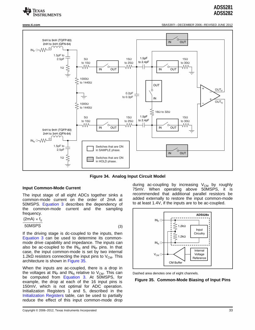

CLKP
CLKN
CMOS Clock Input
01 Fm
01 Fm
CLKP
CLKN
CMOS Single-Ended
Clock
0V
CLKP
CLKN
Differential Sine-Wave
PECL or LVDS Clock Input
01 Fm
01 Fm
5kW 5kW
VCM
CLKP
CLKN
VCM
ADS5281ADS5282
wwwticom SBAS397I ndashDECEMBER 2006ndashREVISED JUNE 2012
CLOCK INPUT
The eight channels on the device operate from asingle ADCLK input To ensure that the aperturedelay and jitter are the same for all channels a clocktree network is used to generate individual samplingclocks to each channel The clock paths for all thechannels are matched from the source point to thesampling circuit This architecture ensures that theperformance and timing for all channels are identicalThe use of the clock tree for matching introduces anaperture delay that is defined as the delay betweenthe rising edge of ADCLK and the actual instant ofsampling The aperture delays for all the channelsare matched to the best possible extent A mismatchof plusmn20ps (plusmn3σ) could exist between the apertureinstants of the eight ADCs within the same chip Figure 39 Internal Clock BufferHowever the aperture delays of ADCs across twodifferent chips can be several hundred picosecondsapart
The ADS528x can be made to operate either inCMOS single-ended clock mode (default isDIFF_CLK = 0) or differential clock mode (SINELVPECL or LVDS) When operating in the single-ended clock mode CLKN must be forced to 0VDCand the single-ended CMOS applied on the CLKP pinThis operation is shown in Figure 38
Figure 40 Differential Clock Driving Circuit(DIFF_CLK = 1)
Figure 38 Single-Ended Clock Driving Circuit(DIFF_CLK = 0)
When configured to operate in the differential clock Figure 41 Single-Ended Clock Driving Circuitmode (register bit DIFF_CLK = 1) the ADS528x clock When DIFF_CLK = 1inputs can be driven differentially (SINE LVPECL orLVDS) with little or no difference in performance
For best performance the clock inputs must bebetween them or with a single-ended (LVCMOS)driven differentially in order to reduce susceptibility toThe common-mode voltage of the clock inputs is setcommon-mode noise For high input frequencyto VCM using internal 5kΩ resistors as shown insampling it is recommended to use a clock sourceFigure 39 This method allows using transformer-with very low jitter Bandpass filtering of the clockcoupled drive circuits for a sine wave clock or ac-source can help reduce the effect of jitter If the dutycoupling for LVPECL and LVDS clock sources ascycle deviates from 50 by more than 2 or 3 it isshown in Figure 40 When operating in the differentialrecommended to enable the DCC through register bitclock mode the single-ended CMOS clock can be ac-EN_DCCcoupled to the CLKP input with CLKN (pin 11)
connected to ground with a 01μF capacitor asshown in Figure 41
Copyright copy 2006ndash2012 Texas Instruments Incorporated 35
Threshold 1 Threshold 2 Threshold 3
10 MHz 45 MHz 65 MHz
Sampling Frequency
ADS5281ADS5282
SBAS397I ndashDECEMBER 2006ndashREVISED JUNE 2012 wwwticom
PLL OPERATION ACROSS SAMPLING Step 2 Disable the PLL automatic switch and setFREQUENCY the PLL configuration depending on the clock
frequencyThe ADS528X uses a PLL for generating the highspeed bit clock (LCLK) the frame clock (ADCLK) amp SAMPLE CLOCK FREQUENCY REGISTER SETTING (Hex)internal clocks for the serializer operation RANGE (MSPS)
Min Max Address DataTo enable operation across the entire frequencyrange the PLL is automatically configured to one of 10 25 E3 0060four states depending on the sampling clock 15 45 E3 00A0frequency range The frequency range detection isautomatic and each time the sampling frequency With the above settings applied for the respectivecrosses a threshold the PLL changes its frequency ranges the part will continue toconfiguration to a new state To prevent unwanted operate as per the stated datasheet specificationstoggling of PLL state around a threshold the circuit for all timing parameters at all specifiedhas an inbuilt hysteresis The ADS528x has three frequencies EXCEPT for the timing specificationsthresholds ndash taking into account the hysteresis range at 40MSPS At 40MSPS the affected parametersof each threshold variation across devices and are ndash Data setup time Data hold time and Clocktemperature the thresholds can span the sampling propagation delay (refer to LVDS Timing )clock frequency range from 10MHz to 45MHz 2 For sampling clock frequency ge 45MSPS
As there are no PLL thresholds beyond 45MHzno change in PLL configuration can occur as thetemperature in the system stabilizes TheADS528x can be used in the system withoutusing the above software fix
INPUT OVER-VOLTAGE RECOVERY
The differential peak-to-peak full-scale rangesupported by the ADS528x is nominally 20V TheADS528x is specially designed to handle an over-
Figure 42 Variation of Thresholds Across voltage condition where the differential peak-to-peakSampling Frequency voltage can be up to twice the ADC full-scale range
If the input common-mode is not considerably offfrom VCM during overload (less than 300mV aroundBased on actual system clock frequency there arethe nominal value of 15V) recovery from an over-two scenariosvoltage pulse input of twice the amplitude of a full-1 For sampling clock frequency lt 45MSPSscale pulse is expected to be within one clock cycle
After system power up depending on the when the input switches from overload to zero signalfrequency of operation and the frequencythreshold for the given device the frequency REFERENCE CIRCUITrange detection circuit may change state once In
The digital beam-forming algorithm in an ultrasoundsome applications where a timing calibrationsystem relies on gain matching across all receivermight be done at the system level once afterchannels A typical system would have about 12 octalpower up this subsequent change of the PLLADCs on the board In such a case it is critical tostate might be undesirable as it can cause a lossensure that the gain is matched essentially requiringof alignment in the received data A software fixthe reference voltages seen by all the ADCs to be thefor eliminating this one-time change of PLL statesame Matching references within the eight channelsexists using the serial register interfaceof a chip is done by using a single internal referencendash Disable the automatic switch of the PLLvoltage buffer Trimming the reference voltages onconfiguration based on frequency detectedeach chip during production ensures that thendash In addition to disabling the switching it is alsoreference voltages are well-matched across differentrequired to set the PLL to the correctchipsconfiguration depending on the sample clock
frequency used in the system All bias currents required for the internal operation ofthe device are set using an external resistor toThe following sequence of register writes must beground at the ISET pin Using a 562kΩ resistor on ISETfollowedgenerates an internal reference current of 20μA This
Step 1 Write Address = 0x01 Data = 0x0010 current is mirrored internally to generate the biascurrent for the internal blocks Using a larger external
36 Copyright copy 2006ndash2012 Texas Instruments Incorporated
VREF = 15V -B
VCM
15V
VREF = 15V +T
VCM
15V
REFT
REFB
ISET
01 Fm 22 Fm
0 to
2
W
W
0 toW
2W
562kW
22 Fm 01 Fm
ADS528x
ADS5281ADS5282
wwwticom SBAS397I ndashDECEMBER 2006ndashREVISED JUNE 2012
resistor at ISET reduces the reference bias current and The device also supports the use of externalthereby scales down the device operating power reference voltages There are two methods to forceHowever it is recommended that the external resistor the references externally The first method involvesbe within 10 of the specified value of 562kΩ so pulling INTEXT low and forcing externally REFT andthat the internal bias margins for the various blocks REFB to 25V and 05V nominally respectively In thisare proper mode the internal reference buffer goes to a 3-state
output The external reference driving circuit shouldBuffering the internal bandgap voltage also generates be designed to provide the required switching currentthe common-mode voltage VCM which is set to the for the eight ADCs inside the chip It should be notedmidlevel of REFT and REFB and is accessible on a that in this mode VCM and ISET continue to bepin (pin 65 in TQFP-80 package pin 53 in QFN-64 generated from the internal bandgap voltage as inpackage) It is meant as a reference voltage to derive the internal reference mode It is therefore importantthe input common-mode if the input is directly to ensure that the common-mode voltage of thecoupled It can also be used to derive the reference externally-forced reference voltages matches tocommon-mode voltage in the external reference within 50mV of VCMmode The suggested decoupling for the referencepins is shown in Figure 43 The second method of forcing the reference voltages
externally can be accessed by pulling INTEXT lowand programming the serial interface to drive theexternal reference mode through the VCM pin (registerbit called EXT_REF_VCM) In this mode VCMbecomes configured as an input pin that can bedriven from external circuitry The internal referencebuffers driving REFT and REFB are active in thismode Forcing 15V on the VCM pin in the moderesults in REFT and REFB coming to 25V and 05Vrespectively In general the voltages on REFT andREFB in this mode are given by Equation 4 andEquation 5 respectively
(4)Figure 43 Suggested Decoupling on the
Reference Pins(5)
The state of the reference voltage internal buffersduring various combinations of the PD INTEXT andEXT_REF_VCM register bits is described in Table 8
Table 8 State of Reference Voltages for Various Combinations of PD INTEXT and EXT_REF_VCM
REGISTER BIT INTERNAL BUFFER STATE
PD 0 0 1 1 0 0 1 1
INTEXT 0 1 0 1 0 1 0 1
EXT_REF_VCM 0 0 0 0 1 1 1 1
REFT buffer 3-state 25V 3-state 25V (1) 15V + VCM15V Do not use 25V (1) Do not use
REFB buffer 3-state 05V 3-state 05V (1) 15V ndash VCM15V Do not use 05V (1) Do not use
VCM pin 15V 15V 15V 15V Force Do not use Force Do not use
(1) Weakly forced with reduced strengthsections while LVDD and LVSS are used to denotethe digital supplies Care is taken to ensure that thereNOISE COUPLING ISSUESis minimal interaction between the supply sets within
High-speed mixed signals are sensitive to various the device The extent of noise coupled andtypes of noise coupling One primary source of noise transmitted from the digital to the analog sectionsis the switching noise from the serializer and the depends onoutput buffers Maximum care is taken to isolate
1 The effective inductances of each of the supplythese noise sources from the sensitive analog blocksand ground setsAs a starting point the analog and digital domains of
2 The isolation between the digital and analogthe device are clearly demarcated AVDD and AVSSsupply and ground setsare used to denote the supplies for the analog
Copyright copy 2006ndash2012 Texas Instruments Incorporated 37
ADS5281ADS5282
SBAS397I ndashDECEMBER 2006ndashREVISED JUNE 2012 wwwticom
Smaller effective inductance of the supply and ground It is recommended that the isolation be maintained onpins leads to better noise suppression For this the board by using separate supplies to drive AVDDreason multiple pins are used to drive each supply and LVDD as well as separate ground planes forand ground It is also critical to ensure that the AVSS and LVSS The use of LVDS buffers reducesimpedances of the supply and ground lines on the the injected noise considerably compared to CMOSboard are kept to the minimum possible values Use buffers The current in the LVDS buffer isof ground planes in the printed circuit board (PCB) as independent of the direction of switching Also thewell as large decoupling capacitors between the low output swing as well as the differential nature ofsupply and ground lines are necessary to obtain the the LVDS buffer results in low-noise couplingbest possible SNR performance from the device
38 Copyright copy 2006ndash2012 Texas Instruments Incorporated
ADS5281ADS5282
wwwticom SBAS397I ndashDECEMBER 2006ndashREVISED JUNE 2012
REVISION HISTORY
Changes from Revision G (March 2008) to Revision H Page
bull Changed second table and conditions in the Initialization Registers section 3
bull Changed In Input Common-Mode Current section changed initialization register 5 to initialization registers 1 and 5to reflect change in Initialization Registers table 33
Changes from Revision F (March 2008) to Revision G Page
bull Deleted note (3) of Ordering Information table to indicate device status is now Production Data for all parts 2
bull Added new note (3) of Ordering Information table to indicate the quantity of transport media is available in thePackage Option Addendum 2
bull Added note (1) to Initialization Registers section to indicate it is no longer necessary to program initializationregisters 1 to 4 3
bull Changed maximum specifications for ADS5282 column in the Power SupplymdashInternal Reference Mode section ofElectrical Characteristics (By Device) table 6
bull Changed minimum specification for ADS5282 column in the f = 10 MHz row of the SNR section of ElectricalCharacteristics (By Device) table 6
Changes from Revision H (March 2008) to Revision I Page
bull Added table in the INITIALIZATION REGISTERS section 3
bull Added table in the LVDS OUTPUT TIMING CHARACTERISTICS section 14
bull Added PLL OPERATION ACROSS SAMPLING FREQUENCY section 36
Copyright copy 2006ndash2012 Texas Instruments Incorporated 39
PACKAGE OPTION ADDENDUM
wwwticom 26-Oct-2016
Addendum-Page 1
PACKAGING INFORMATION
Orderable Device Status(1)
Package Type PackageDrawing
Pins PackageQty
Eco Plan(2)
LeadBall Finish(6)
MSL Peak Temp(3)
Op Temp (degC) Device Marking(45)
Samples
ADS5281IPFP ACTIVE HTQFP PFP 80 96 Green (RoHSamp no SbBr)
CU NIPDAU Level-3-260C-168 HR -40 to 85 ADS5281I
ADS5281IPFPR ACTIVE HTQFP PFP 80 1000 Green (RoHSamp no SbBr)
CU NIPDAU Level-3-260C-168 HR -40 to 85 ADS5281I
ADS5281IRGCR ACTIVE VQFN RGC 64 2000 Green (RoHSamp no SbBr)
CU NIPDAU Level-3-260C-168 HR -40 to 85 AZ5281
ADS5281IRGCT ACTIVE VQFN RGC 64 250 Green (RoHSamp no SbBr)
CU NIPDAU Level-3-260C-168 HR -40 to 85 AZ5281
ADS5282IRGCR ACTIVE VQFN RGC 64 2000 Green (RoHSamp no SbBr)
CU NIPDAU Level-3-260C-168 HR -40 to 85 AZ5282
ADS5282IRGCT ACTIVE VQFN RGC 64 250 Green (RoHSamp no SbBr)
CU NIPDAU Level-3-260C-168 HR -40 to 85 AZ5282
(1) The marketing status values are defined as followsACTIVE Product device recommended for new designsLIFEBUY TI has announced that the device will be discontinued and a lifetime-buy period is in effectNRND Not recommended for new designs Device is in production to support existing customers but TI does not recommend using this part in a new designPREVIEW Device has been announced but is not in production Samples may or may not be availableOBSOLETE TI has discontinued the production of the device
(2) Eco Plan - The planned eco-friendly classification Pb-Free (RoHS) Pb-Free (RoHS Exempt) or Green (RoHS amp no SbBr) - please check httpwwwticomproductcontent for the latest availabilityinformation and additional product content detailsTBD The Pb-FreeGreen conversion plan has not been definedPb-Free (RoHS) TIs terms Lead-Free or Pb-Free mean semiconductor products that are compatible with the current RoHS requirements for all 6 substances including the requirement thatlead not exceed 01 by weight in homogeneous materials Where designed to be soldered at high temperatures TI Pb-Free products are suitable for use in specified lead-free processesPb-Free (RoHS Exempt) This component has a RoHS exemption for either 1) lead-based flip-chip solder bumps used between the die and package or 2) lead-based die adhesive used betweenthe die and leadframe The component is otherwise considered Pb-Free (RoHS compatible) as defined aboveGreen (RoHS amp no SbBr) TI defines Green to mean Pb-Free (RoHS compatible) and free of Bromine (Br) and Antimony (Sb) based flame retardants (Br or Sb do not exceed 01 by weightin homogeneous material)
(3) MSL Peak Temp - The Moisture Sensitivity Level rating according to the JEDEC industry standard classifications and peak solder temperature
(4) There may be additional marking which relates to the logo the lot trace code information or the environmental category on the device
(5) Multiple Device Markings will be inside parentheses Only one Device Marking contained in parentheses and separated by a ~ will appear on a device If a line is indented then it is a continuationof the previous line and the two combined represent the entire Device Marking for that device
PACKAGE OPTION ADDENDUM
wwwticom 26-Oct-2016
Addendum-Page 2
(6) LeadBall Finish - Orderable Devices may have multiple material finish options Finish options are separated by a vertical ruled line LeadBall Finish values may wrap to two lines if the finishvalue exceeds the maximum column width
Important Information and DisclaimerThe information provided on this page represents TIs knowledge and belief as of the date that it is provided TI bases its knowledge and belief on informationprovided by third parties and makes no representation or warranty as to the accuracy of such information Efforts are underway to better integrate information from third parties TI has taken andcontinues to take reasonable steps to provide representative and accurate information but may not have conducted destructive testing or chemical analysis on incoming materials and chemicalsTI and TI suppliers consider certain information to be proprietary and thus CAS numbers and other limited information may not be available for release
In no event shall TIs liability arising out of such information exceed the total purchase price of the TI part(s) at issue in this document sold by TI to Customer on an annual basis
TAPE AND REEL INFORMATION
All dimensions are nominal
Device PackageType
PackageDrawing
Pins SPQ ReelDiameter
(mm)
ReelWidth
W1 (mm)
A0(mm)
B0(mm)
K0(mm)
P1(mm)
W(mm)
Pin1Quadrant
ADS5281IPFPR HTQFP PFP 80 1000 3300 244 150 150 15 200 240 Q2
ADS5281IRGCR VQFN RGC 64 2000 3300 164 93 93 15 120 160 Q2
ADS5281IRGCT VQFN RGC 64 250 1800 164 93 93 15 120 160 Q2
ADS5282IRGCR VQFN RGC 64 2000 3300 164 93 93 15 120 160 Q2
ADS5282IRGCT VQFN RGC 64 250 1800 164 93 93 15 120 160 Q2
PACKAGE MATERIALS INFORMATION
wwwticom 14-May-2015
Pack Materials-Page 1
All dimensions are nominal
Device Package Type Package Drawing Pins SPQ Length (mm) Width (mm) Height (mm)
ADS5281IPFPR HTQFP PFP 80 1000 3670 3670 450
ADS5281IRGCR VQFN RGC 64 2000 3366 3366 286
ADS5281IRGCT VQFN RGC 64 250 2130 1910 550
ADS5282IRGCR VQFN RGC 64 2000 3366 3366 286
ADS5282IRGCT VQFN RGC 64 250 2130 1910 550
PACKAGE MATERIALS INFORMATION
wwwticom 14-May-2015
Pack Materials-Page 2
wwwticom
IMPORTANT NOTICE
Texas Instruments Incorporated and its subsidiaries (TI) reserve the right to make corrections enhancements improvements and otherchanges to its semiconductor products and services per JESD46 latest issue and to discontinue any product or service per JESD48 latestissue Buyers should obtain the latest relevant information before placing orders and should verify that such information is current andcomplete All semiconductor products (also referred to herein as ldquocomponentsrdquo) are sold subject to TIrsquos terms and conditions of salesupplied at the time of order acknowledgmentTI warrants performance of its components to the specifications applicable at the time of sale in accordance with the warranty in TIrsquos termsand conditions of sale of semiconductor products Testing and other quality control techniques are used to the extent TI deems necessaryto support this warranty Except where mandated by applicable law testing of all parameters of each component is not necessarilyperformedTI assumes no liability for applications assistance or the design of Buyersrsquo products Buyers are responsible for their products andapplications using TI components To minimize the risks associated with Buyersrsquo products and applications Buyers should provideadequate design and operating safeguardsTI does not warrant or represent that any license either express or implied is granted under any patent right copyright mask work right orother intellectual property right relating to any combination machine or process in which TI components or services are used Informationpublished by TI regarding third-party products or services does not constitute a license to use such products or services or a warranty orendorsement thereof Use of such information may require a license from a third party under the patents or other intellectual property of thethird party or a license from TI under the patents or other intellectual property of TIReproduction of significant portions of TI information in TI data books or data sheets is permissible only if reproduction is without alterationand is accompanied by all associated warranties conditions limitations and notices TI is not responsible or liable for such altereddocumentation Information of third parties may be subject to additional restrictionsResale of TI components or services with statements different from or beyond the parameters stated by TI for that component or servicevoids all express and any implied warranties for the associated TI component or service and is an unfair and deceptive business practiceTI is not responsible or liable for any such statementsBuyer acknowledges and agrees that it is solely responsible for compliance with all legal regulatory and safety-related requirementsconcerning its products and any use of TI components in its applications notwithstanding any applications-related information or supportthat may be provided by TI Buyer represents and agrees that it has all the necessary expertise to create and implement safeguards whichanticipate dangerous consequences of failures monitor failures and their consequences lessen the likelihood of failures that might causeharm and take appropriate remedial actions Buyer will fully indemnify TI and its representatives against any damages arising out of the useof any TI components in safety-critical applicationsIn some cases TI components may be promoted specifically to facilitate safety-related applications With such components TIrsquos goal is tohelp enable customers to design and create their own end-product solutions that meet applicable functional safety standards andrequirements Nonetheless such components are subject to these termsNo TI components are authorized for use in FDA Class III (or similar life-critical medical equipment) unless authorized officers of the partieshave executed a special agreement specifically governing such useOnly those TI components which TI has specifically designated as military grade or ldquoenhanced plasticrdquo are designed and intended for use inmilitaryaerospace applications or environments Buyer acknowledges and agrees that any military or aerospace use of TI componentswhich have not been so designated is solely at the Buyers risk and that Buyer is solely responsible for compliance with all legal andregulatory requirements in connection with such useTI has specifically designated certain components as meeting ISOTS16949 requirements mainly for automotive use In any case of use ofnon-designated products TI will not be responsible for any failure to meet ISOTS16949
Products ApplicationsAudio wwwticomaudio Automotive and Transportation wwwticomautomotiveAmplifiers amplifierticom Communications and Telecom wwwticomcommunicationsData Converters dataconverterticom Computers and Peripherals wwwticomcomputersDLPreg Products wwwdlpcom Consumer Electronics wwwticomconsumer-appsDSP dspticom Energy and Lighting wwwticomenergyClocks and Timers wwwticomclocks Industrial wwwticomindustrialInterface interfaceticom Medical wwwticommedicalLogic logicticom Security wwwticomsecurityPower Mgmt powerticom Space Avionics and Defense wwwticomspace-avionics-defenseMicrocontrollers microcontrollerticom Video and Imaging wwwticomvideoRFID wwwti-rfidcomOMAP Applications Processors wwwticomomap TI E2E Community e2eticomWireless Connectivity wwwticomwirelessconnectivity
Mailing Address Texas Instruments Post Office Box 655303 Dallas Texas 75265Copyright copy 2016 Texas Instruments Incorporated
- FEATURES
- APPLICATIONS
- DESCRIPTION
- ABSOLUTE MAXIMUM RATINGS
- RECOMMENDED OPERATING CONDITIONS
- INITIALIZATION REGISTERS
- DIGITAL CHARACTERISTICS
- ELECTRICAL CHARACTERISTICS
- ELECTRICAL CHARACTERISTICS (BY DEVICE)
- PIN CONFIGURATIONS
- FUNCTIONAL BLOCK DIAGRAM
- TIMING CHARACTERISTICS
- LVDS OUTPUT TIMING CHARACTERISTICS
- LVDS OUTPUT TIMING CHARACTERISTICS
- LVDS OUTPUT TIMING CHARACTERISTICS
- SERIAL INTERFACE
-
- Register Initialization
-
- SERIAL REGISTER MAP
- SUMMARY OF FEATURES
- DESCRIPTION OF SERIAL REGISTERS
-
- SOFTWARE RESET
- POWER-DOWN MODES
- LVDS DRIVE PROGRAMMABILITY
- LVDS INTERNAL TERMINATION PROGRAMMABILITY
- LOW-FREQUENCY NOISE SUPPRESSION MODE
- ANALOG INPUT INVERT
- LVDS TEST PATTERNS
- PROGRAMMABLE GAIN
- CLOCK REFERENCE AND DATA OUTPUT MODES
-
- INPUT CLOCK
- EXTERNAL REFERENCE
- BIT CLOCK PROGRAMMABILITY
- DATA OUTPUT FORMAT MODES
-
- TYPICAL CHARACTERISTICS
- APPLICATION INFORMATION
-
- THEORY OF OPERATION
- ANALOG INPUT
-
- Input Common-Mode Current
- Driving Circuit
-
- CLOCK INPUT
- PLL OPERATION ACROSS SAMPLING FREQUENCY
- INPUT OVER-VOLTAGE RECOVERY
- REFERENCE CIRCUIT
- NOISE COUPLING ISSUES
-
- Revision History
-
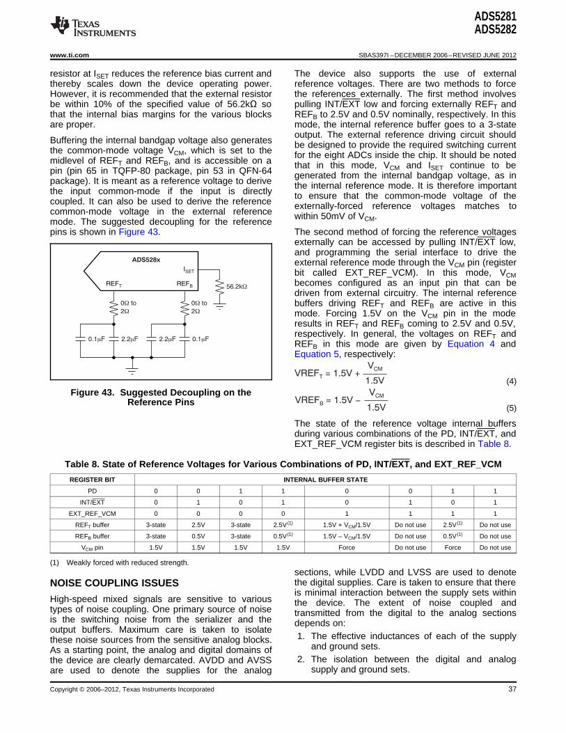
ADS5281ADS5282
SBAS397I ndashDECEMBER 2006ndashREVISED JUNE 2012 wwwticom
Smaller effective inductance of the supply and ground It is recommended that the isolation be maintained onpins leads to better noise suppression For this the board by using separate supplies to drive AVDDreason multiple pins are used to drive each supply and LVDD as well as separate ground planes forand ground It is also critical to ensure that the AVSS and LVSS The use of LVDS buffers reducesimpedances of the supply and ground lines on the the injected noise considerably compared to CMOSboard are kept to the minimum possible values Use buffers The current in the LVDS buffer isof ground planes in the printed circuit board (PCB) as independent of the direction of switching Also thewell as large decoupling capacitors between the low output swing as well as the differential nature ofsupply and ground lines are necessary to obtain the the LVDS buffer results in low-noise couplingbest possible SNR performance from the device
38 Copyright copy 2006ndash2012 Texas Instruments Incorporated
ADS5281ADS5282
wwwticom SBAS397I ndashDECEMBER 2006ndashREVISED JUNE 2012
REVISION HISTORY
Changes from Revision G (March 2008) to Revision H Page
bull Changed second table and conditions in the Initialization Registers section 3
bull Changed In Input Common-Mode Current section changed initialization register 5 to initialization registers 1 and 5to reflect change in Initialization Registers table 33
Changes from Revision F (March 2008) to Revision G Page
bull Deleted note (3) of Ordering Information table to indicate device status is now Production Data for all parts 2
bull Added new note (3) of Ordering Information table to indicate the quantity of transport media is available in thePackage Option Addendum 2
bull Added note (1) to Initialization Registers section to indicate it is no longer necessary to program initializationregisters 1 to 4 3
bull Changed maximum specifications for ADS5282 column in the Power SupplymdashInternal Reference Mode section ofElectrical Characteristics (By Device) table 6
bull Changed minimum specification for ADS5282 column in the f = 10 MHz row of the SNR section of ElectricalCharacteristics (By Device) table 6
Changes from Revision H (March 2008) to Revision I Page
bull Added table in the INITIALIZATION REGISTERS section 3
bull Added table in the LVDS OUTPUT TIMING CHARACTERISTICS section 14
bull Added PLL OPERATION ACROSS SAMPLING FREQUENCY section 36
Copyright copy 2006ndash2012 Texas Instruments Incorporated 39
PACKAGE OPTION ADDENDUM
wwwticom 26-Oct-2016
Addendum-Page 1
PACKAGING INFORMATION
Orderable Device Status(1)
Package Type PackageDrawing
Pins PackageQty
Eco Plan(2)
LeadBall Finish(6)
MSL Peak Temp(3)
Op Temp (degC) Device Marking(45)
Samples
ADS5281IPFP ACTIVE HTQFP PFP 80 96 Green (RoHSamp no SbBr)
CU NIPDAU Level-3-260C-168 HR -40 to 85 ADS5281I
ADS5281IPFPR ACTIVE HTQFP PFP 80 1000 Green (RoHSamp no SbBr)
CU NIPDAU Level-3-260C-168 HR -40 to 85 ADS5281I
ADS5281IRGCR ACTIVE VQFN RGC 64 2000 Green (RoHSamp no SbBr)
CU NIPDAU Level-3-260C-168 HR -40 to 85 AZ5281
ADS5281IRGCT ACTIVE VQFN RGC 64 250 Green (RoHSamp no SbBr)
CU NIPDAU Level-3-260C-168 HR -40 to 85 AZ5281
ADS5282IRGCR ACTIVE VQFN RGC 64 2000 Green (RoHSamp no SbBr)
CU NIPDAU Level-3-260C-168 HR -40 to 85 AZ5282
ADS5282IRGCT ACTIVE VQFN RGC 64 250 Green (RoHSamp no SbBr)
CU NIPDAU Level-3-260C-168 HR -40 to 85 AZ5282
(1) The marketing status values are defined as followsACTIVE Product device recommended for new designsLIFEBUY TI has announced that the device will be discontinued and a lifetime-buy period is in effectNRND Not recommended for new designs Device is in production to support existing customers but TI does not recommend using this part in a new designPREVIEW Device has been announced but is not in production Samples may or may not be availableOBSOLETE TI has discontinued the production of the device
(2) Eco Plan - The planned eco-friendly classification Pb-Free (RoHS) Pb-Free (RoHS Exempt) or Green (RoHS amp no SbBr) - please check httpwwwticomproductcontent for the latest availabilityinformation and additional product content detailsTBD The Pb-FreeGreen conversion plan has not been definedPb-Free (RoHS) TIs terms Lead-Free or Pb-Free mean semiconductor products that are compatible with the current RoHS requirements for all 6 substances including the requirement thatlead not exceed 01 by weight in homogeneous materials Where designed to be soldered at high temperatures TI Pb-Free products are suitable for use in specified lead-free processesPb-Free (RoHS Exempt) This component has a RoHS exemption for either 1) lead-based flip-chip solder bumps used between the die and package or 2) lead-based die adhesive used betweenthe die and leadframe The component is otherwise considered Pb-Free (RoHS compatible) as defined aboveGreen (RoHS amp no SbBr) TI defines Green to mean Pb-Free (RoHS compatible) and free of Bromine (Br) and Antimony (Sb) based flame retardants (Br or Sb do not exceed 01 by weightin homogeneous material)
(3) MSL Peak Temp - The Moisture Sensitivity Level rating according to the JEDEC industry standard classifications and peak solder temperature
(4) There may be additional marking which relates to the logo the lot trace code information or the environmental category on the device
(5) Multiple Device Markings will be inside parentheses Only one Device Marking contained in parentheses and separated by a ~ will appear on a device If a line is indented then it is a continuationof the previous line and the two combined represent the entire Device Marking for that device
PACKAGE OPTION ADDENDUM
wwwticom 26-Oct-2016
Addendum-Page 2
(6) LeadBall Finish - Orderable Devices may have multiple material finish options Finish options are separated by a vertical ruled line LeadBall Finish values may wrap to two lines if the finishvalue exceeds the maximum column width
Important Information and DisclaimerThe information provided on this page represents TIs knowledge and belief as of the date that it is provided TI bases its knowledge and belief on informationprovided by third parties and makes no representation or warranty as to the accuracy of such information Efforts are underway to better integrate information from third parties TI has taken andcontinues to take reasonable steps to provide representative and accurate information but may not have conducted destructive testing or chemical analysis on incoming materials and chemicalsTI and TI suppliers consider certain information to be proprietary and thus CAS numbers and other limited information may not be available for release
In no event shall TIs liability arising out of such information exceed the total purchase price of the TI part(s) at issue in this document sold by TI to Customer on an annual basis
TAPE AND REEL INFORMATION
All dimensions are nominal
Device PackageType
PackageDrawing
Pins SPQ ReelDiameter
(mm)
ReelWidth
W1 (mm)
A0(mm)
B0(mm)
K0(mm)
P1(mm)
W(mm)
Pin1Quadrant
ADS5281IPFPR HTQFP PFP 80 1000 3300 244 150 150 15 200 240 Q2
ADS5281IRGCR VQFN RGC 64 2000 3300 164 93 93 15 120 160 Q2
ADS5281IRGCT VQFN RGC 64 250 1800 164 93 93 15 120 160 Q2
ADS5282IRGCR VQFN RGC 64 2000 3300 164 93 93 15 120 160 Q2
ADS5282IRGCT VQFN RGC 64 250 1800 164 93 93 15 120 160 Q2
PACKAGE MATERIALS INFORMATION
wwwticom 14-May-2015
Pack Materials-Page 1
All dimensions are nominal
Device Package Type Package Drawing Pins SPQ Length (mm) Width (mm) Height (mm)
ADS5281IPFPR HTQFP PFP 80 1000 3670 3670 450
ADS5281IRGCR VQFN RGC 64 2000 3366 3366 286
ADS5281IRGCT VQFN RGC 64 250 2130 1910 550
ADS5282IRGCR VQFN RGC 64 2000 3366 3366 286
ADS5282IRGCT VQFN RGC 64 250 2130 1910 550
PACKAGE MATERIALS INFORMATION
wwwticom 14-May-2015
Pack Materials-Page 2
wwwticom
IMPORTANT NOTICE
Texas Instruments Incorporated and its subsidiaries (TI) reserve the right to make corrections enhancements improvements and otherchanges to its semiconductor products and services per JESD46 latest issue and to discontinue any product or service per JESD48 latestissue Buyers should obtain the latest relevant information before placing orders and should verify that such information is current andcomplete All semiconductor products (also referred to herein as ldquocomponentsrdquo) are sold subject to TIrsquos terms and conditions of salesupplied at the time of order acknowledgmentTI warrants performance of its components to the specifications applicable at the time of sale in accordance with the warranty in TIrsquos termsand conditions of sale of semiconductor products Testing and other quality control techniques are used to the extent TI deems necessaryto support this warranty Except where mandated by applicable law testing of all parameters of each component is not necessarilyperformedTI assumes no liability for applications assistance or the design of Buyersrsquo products Buyers are responsible for their products andapplications using TI components To minimize the risks associated with Buyersrsquo products and applications Buyers should provideadequate design and operating safeguardsTI does not warrant or represent that any license either express or implied is granted under any patent right copyright mask work right orother intellectual property right relating to any combination machine or process in which TI components or services are used Informationpublished by TI regarding third-party products or services does not constitute a license to use such products or services or a warranty orendorsement thereof Use of such information may require a license from a third party under the patents or other intellectual property of thethird party or a license from TI under the patents or other intellectual property of TIReproduction of significant portions of TI information in TI data books or data sheets is permissible only if reproduction is without alterationand is accompanied by all associated warranties conditions limitations and notices TI is not responsible or liable for such altereddocumentation Information of third parties may be subject to additional restrictionsResale of TI components or services with statements different from or beyond the parameters stated by TI for that component or servicevoids all express and any implied warranties for the associated TI component or service and is an unfair and deceptive business practiceTI is not responsible or liable for any such statementsBuyer acknowledges and agrees that it is solely responsible for compliance with all legal regulatory and safety-related requirementsconcerning its products and any use of TI components in its applications notwithstanding any applications-related information or supportthat may be provided by TI Buyer represents and agrees that it has all the necessary expertise to create and implement safeguards whichanticipate dangerous consequences of failures monitor failures and their consequences lessen the likelihood of failures that might causeharm and take appropriate remedial actions Buyer will fully indemnify TI and its representatives against any damages arising out of the useof any TI components in safety-critical applicationsIn some cases TI components may be promoted specifically to facilitate safety-related applications With such components TIrsquos goal is tohelp enable customers to design and create their own end-product solutions that meet applicable functional safety standards andrequirements Nonetheless such components are subject to these termsNo TI components are authorized for use in FDA Class III (or similar life-critical medical equipment) unless authorized officers of the partieshave executed a special agreement specifically governing such useOnly those TI components which TI has specifically designated as military grade or ldquoenhanced plasticrdquo are designed and intended for use inmilitaryaerospace applications or environments Buyer acknowledges and agrees that any military or aerospace use of TI componentswhich have not been so designated is solely at the Buyers risk and that Buyer is solely responsible for compliance with all legal andregulatory requirements in connection with such useTI has specifically designated certain components as meeting ISOTS16949 requirements mainly for automotive use In any case of use ofnon-designated products TI will not be responsible for any failure to meet ISOTS16949
Products ApplicationsAudio wwwticomaudio Automotive and Transportation wwwticomautomotiveAmplifiers amplifierticom Communications and Telecom wwwticomcommunicationsData Converters dataconverterticom Computers and Peripherals wwwticomcomputersDLPreg Products wwwdlpcom Consumer Electronics wwwticomconsumer-appsDSP dspticom Energy and Lighting wwwticomenergyClocks and Timers wwwticomclocks Industrial wwwticomindustrialInterface interfaceticom Medical wwwticommedicalLogic logicticom Security wwwticomsecurityPower Mgmt powerticom Space Avionics and Defense wwwticomspace-avionics-defenseMicrocontrollers microcontrollerticom Video and Imaging wwwticomvideoRFID wwwti-rfidcomOMAP Applications Processors wwwticomomap TI E2E Community e2eticomWireless Connectivity wwwticomwirelessconnectivity
Mailing Address Texas Instruments Post Office Box 655303 Dallas Texas 75265Copyright copy 2016 Texas Instruments Incorporated
- FEATURES
- APPLICATIONS
- DESCRIPTION
- ABSOLUTE MAXIMUM RATINGS
- RECOMMENDED OPERATING CONDITIONS
- INITIALIZATION REGISTERS
- DIGITAL CHARACTERISTICS
- ELECTRICAL CHARACTERISTICS
- ELECTRICAL CHARACTERISTICS (BY DEVICE)
- PIN CONFIGURATIONS
- FUNCTIONAL BLOCK DIAGRAM
- TIMING CHARACTERISTICS
- LVDS OUTPUT TIMING CHARACTERISTICS
- LVDS OUTPUT TIMING CHARACTERISTICS
- LVDS OUTPUT TIMING CHARACTERISTICS
- SERIAL INTERFACE
-
- Register Initialization
-
- SERIAL REGISTER MAP
- SUMMARY OF FEATURES
- DESCRIPTION OF SERIAL REGISTERS
-
- SOFTWARE RESET
- POWER-DOWN MODES
- LVDS DRIVE PROGRAMMABILITY
- LVDS INTERNAL TERMINATION PROGRAMMABILITY
- LOW-FREQUENCY NOISE SUPPRESSION MODE
- ANALOG INPUT INVERT
- LVDS TEST PATTERNS
- PROGRAMMABLE GAIN
- CLOCK REFERENCE AND DATA OUTPUT MODES
-
- INPUT CLOCK
- EXTERNAL REFERENCE
- BIT CLOCK PROGRAMMABILITY
- DATA OUTPUT FORMAT MODES
-
- TYPICAL CHARACTERISTICS
- APPLICATION INFORMATION
-
- THEORY OF OPERATION
- ANALOG INPUT
-
- Input Common-Mode Current
- Driving Circuit
-
- CLOCK INPUT
- PLL OPERATION ACROSS SAMPLING FREQUENCY
- INPUT OVER-VOLTAGE RECOVERY
- REFERENCE CIRCUIT
- NOISE COUPLING ISSUES
-
- Revision History
-
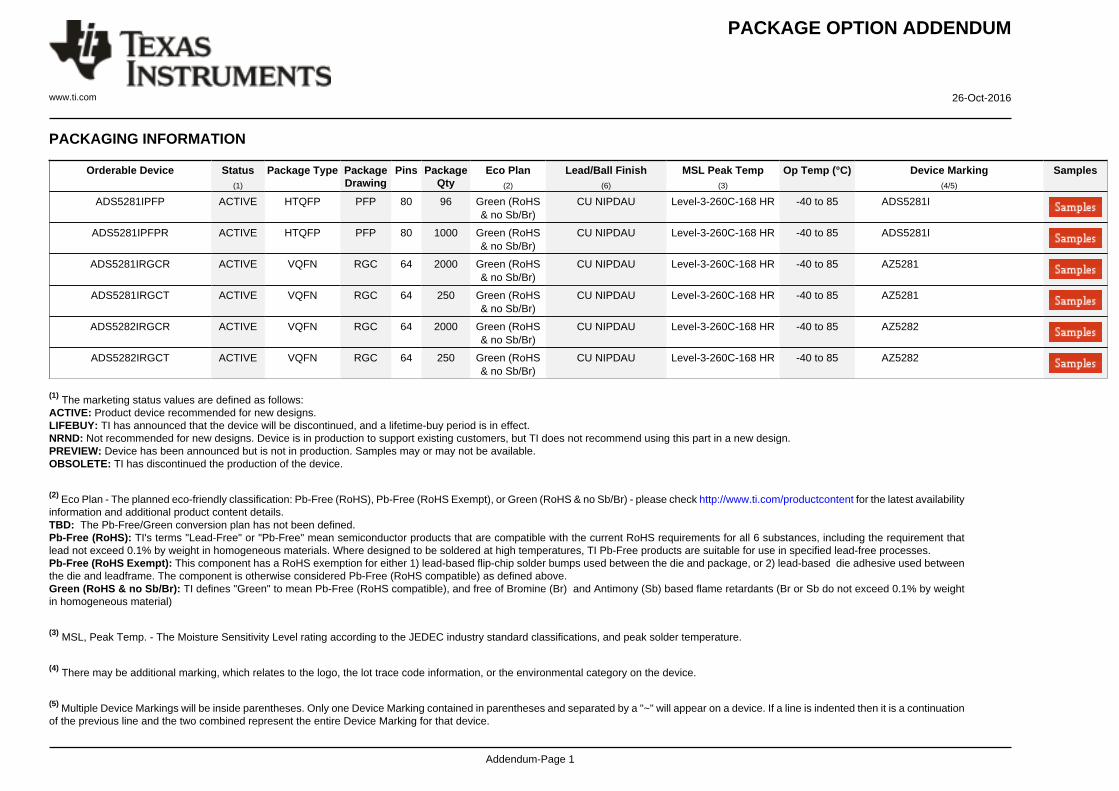
PACKAGE OPTION ADDENDUM
wwwticom 26-Oct-2016
Addendum-Page 1
PACKAGING INFORMATION
Orderable Device Status(1)
Package Type PackageDrawing
Pins PackageQty
Eco Plan(2)
LeadBall Finish(6)
MSL Peak Temp(3)
Op Temp (degC) Device Marking(45)
Samples
ADS5281IPFP ACTIVE HTQFP PFP 80 96 Green (RoHSamp no SbBr)
CU NIPDAU Level-3-260C-168 HR -40 to 85 ADS5281I
ADS5281IPFPR ACTIVE HTQFP PFP 80 1000 Green (RoHSamp no SbBr)
CU NIPDAU Level-3-260C-168 HR -40 to 85 ADS5281I
ADS5281IRGCR ACTIVE VQFN RGC 64 2000 Green (RoHSamp no SbBr)
CU NIPDAU Level-3-260C-168 HR -40 to 85 AZ5281
ADS5281IRGCT ACTIVE VQFN RGC 64 250 Green (RoHSamp no SbBr)
CU NIPDAU Level-3-260C-168 HR -40 to 85 AZ5281
ADS5282IRGCR ACTIVE VQFN RGC 64 2000 Green (RoHSamp no SbBr)
CU NIPDAU Level-3-260C-168 HR -40 to 85 AZ5282
ADS5282IRGCT ACTIVE VQFN RGC 64 250 Green (RoHSamp no SbBr)
CU NIPDAU Level-3-260C-168 HR -40 to 85 AZ5282
(1) The marketing status values are defined as followsACTIVE Product device recommended for new designsLIFEBUY TI has announced that the device will be discontinued and a lifetime-buy period is in effectNRND Not recommended for new designs Device is in production to support existing customers but TI does not recommend using this part in a new designPREVIEW Device has been announced but is not in production Samples may or may not be availableOBSOLETE TI has discontinued the production of the device
(2) Eco Plan - The planned eco-friendly classification Pb-Free (RoHS) Pb-Free (RoHS Exempt) or Green (RoHS amp no SbBr) - please check httpwwwticomproductcontent for the latest availabilityinformation and additional product content detailsTBD The Pb-FreeGreen conversion plan has not been definedPb-Free (RoHS) TIs terms Lead-Free or Pb-Free mean semiconductor products that are compatible with the current RoHS requirements for all 6 substances including the requirement thatlead not exceed 01 by weight in homogeneous materials Where designed to be soldered at high temperatures TI Pb-Free products are suitable for use in specified lead-free processesPb-Free (RoHS Exempt) This component has a RoHS exemption for either 1) lead-based flip-chip solder bumps used between the die and package or 2) lead-based die adhesive used betweenthe die and leadframe The component is otherwise considered Pb-Free (RoHS compatible) as defined aboveGreen (RoHS amp no SbBr) TI defines Green to mean Pb-Free (RoHS compatible) and free of Bromine (Br) and Antimony (Sb) based flame retardants (Br or Sb do not exceed 01 by weightin homogeneous material)
(3) MSL Peak Temp - The Moisture Sensitivity Level rating according to the JEDEC industry standard classifications and peak solder temperature
(4) There may be additional marking which relates to the logo the lot trace code information or the environmental category on the device
(5) Multiple Device Markings will be inside parentheses Only one Device Marking contained in parentheses and separated by a ~ will appear on a device If a line is indented then it is a continuationof the previous line and the two combined represent the entire Device Marking for that device
PACKAGE OPTION ADDENDUM
wwwticom 26-Oct-2016
Addendum-Page 2
(6) LeadBall Finish - Orderable Devices may have multiple material finish options Finish options are separated by a vertical ruled line LeadBall Finish values may wrap to two lines if the finishvalue exceeds the maximum column width
Important Information and DisclaimerThe information provided on this page represents TIs knowledge and belief as of the date that it is provided TI bases its knowledge and belief on informationprovided by third parties and makes no representation or warranty as to the accuracy of such information Efforts are underway to better integrate information from third parties TI has taken andcontinues to take reasonable steps to provide representative and accurate information but may not have conducted destructive testing or chemical analysis on incoming materials and chemicalsTI and TI suppliers consider certain information to be proprietary and thus CAS numbers and other limited information may not be available for release
In no event shall TIs liability arising out of such information exceed the total purchase price of the TI part(s) at issue in this document sold by TI to Customer on an annual basis
TAPE AND REEL INFORMATION
All dimensions are nominal
Device PackageType
PackageDrawing
Pins SPQ ReelDiameter
(mm)
ReelWidth
W1 (mm)
A0(mm)
B0(mm)
K0(mm)
P1(mm)
W(mm)
Pin1Quadrant
ADS5281IPFPR HTQFP PFP 80 1000 3300 244 150 150 15 200 240 Q2
ADS5281IRGCR VQFN RGC 64 2000 3300 164 93 93 15 120 160 Q2
ADS5281IRGCT VQFN RGC 64 250 1800 164 93 93 15 120 160 Q2
ADS5282IRGCR VQFN RGC 64 2000 3300 164 93 93 15 120 160 Q2
ADS5282IRGCT VQFN RGC 64 250 1800 164 93 93 15 120 160 Q2
PACKAGE MATERIALS INFORMATION
wwwticom 14-May-2015
Pack Materials-Page 1
All dimensions are nominal
Device Package Type Package Drawing Pins SPQ Length (mm) Width (mm) Height (mm)
ADS5281IPFPR HTQFP PFP 80 1000 3670 3670 450
ADS5281IRGCR VQFN RGC 64 2000 3366 3366 286
ADS5281IRGCT VQFN RGC 64 250 2130 1910 550
ADS5282IRGCR VQFN RGC 64 2000 3366 3366 286
ADS5282IRGCT VQFN RGC 64 250 2130 1910 550
PACKAGE MATERIALS INFORMATION
wwwticom 14-May-2015
Pack Materials-Page 2
wwwticom
IMPORTANT NOTICE
Texas Instruments Incorporated and its subsidiaries (TI) reserve the right to make corrections enhancements improvements and otherchanges to its semiconductor products and services per JESD46 latest issue and to discontinue any product or service per JESD48 latestissue Buyers should obtain the latest relevant information before placing orders and should verify that such information is current andcomplete All semiconductor products (also referred to herein as ldquocomponentsrdquo) are sold subject to TIrsquos terms and conditions of salesupplied at the time of order acknowledgmentTI warrants performance of its components to the specifications applicable at the time of sale in accordance with the warranty in TIrsquos termsand conditions of sale of semiconductor products Testing and other quality control techniques are used to the extent TI deems necessaryto support this warranty Except where mandated by applicable law testing of all parameters of each component is not necessarilyperformedTI assumes no liability for applications assistance or the design of Buyersrsquo products Buyers are responsible for their products andapplications using TI components To minimize the risks associated with Buyersrsquo products and applications Buyers should provideadequate design and operating safeguardsTI does not warrant or represent that any license either express or implied is granted under any patent right copyright mask work right orother intellectual property right relating to any combination machine or process in which TI components or services are used Informationpublished by TI regarding third-party products or services does not constitute a license to use such products or services or a warranty orendorsement thereof Use of such information may require a license from a third party under the patents or other intellectual property of thethird party or a license from TI under the patents or other intellectual property of TIReproduction of significant portions of TI information in TI data books or data sheets is permissible only if reproduction is without alterationand is accompanied by all associated warranties conditions limitations and notices TI is not responsible or liable for such altereddocumentation Information of third parties may be subject to additional restrictionsResale of TI components or services with statements different from or beyond the parameters stated by TI for that component or servicevoids all express and any implied warranties for the associated TI component or service and is an unfair and deceptive business practiceTI is not responsible or liable for any such statementsBuyer acknowledges and agrees that it is solely responsible for compliance with all legal regulatory and safety-related requirementsconcerning its products and any use of TI components in its applications notwithstanding any applications-related information or supportthat may be provided by TI Buyer represents and agrees that it has all the necessary expertise to create and implement safeguards whichanticipate dangerous consequences of failures monitor failures and their consequences lessen the likelihood of failures that might causeharm and take appropriate remedial actions Buyer will fully indemnify TI and its representatives against any damages arising out of the useof any TI components in safety-critical applicationsIn some cases TI components may be promoted specifically to facilitate safety-related applications With such components TIrsquos goal is tohelp enable customers to design and create their own end-product solutions that meet applicable functional safety standards andrequirements Nonetheless such components are subject to these termsNo TI components are authorized for use in FDA Class III (or similar life-critical medical equipment) unless authorized officers of the partieshave executed a special agreement specifically governing such useOnly those TI components which TI has specifically designated as military grade or ldquoenhanced plasticrdquo are designed and intended for use inmilitaryaerospace applications or environments Buyer acknowledges and agrees that any military or aerospace use of TI componentswhich have not been so designated is solely at the Buyers risk and that Buyer is solely responsible for compliance with all legal andregulatory requirements in connection with such useTI has specifically designated certain components as meeting ISOTS16949 requirements mainly for automotive use In any case of use ofnon-designated products TI will not be responsible for any failure to meet ISOTS16949
Products ApplicationsAudio wwwticomaudio Automotive and Transportation wwwticomautomotiveAmplifiers amplifierticom Communications and Telecom wwwticomcommunicationsData Converters dataconverterticom Computers and Peripherals wwwticomcomputersDLPreg Products wwwdlpcom Consumer Electronics wwwticomconsumer-appsDSP dspticom Energy and Lighting wwwticomenergyClocks and Timers wwwticomclocks Industrial wwwticomindustrialInterface interfaceticom Medical wwwticommedicalLogic logicticom Security wwwticomsecurityPower Mgmt powerticom Space Avionics and Defense wwwticomspace-avionics-defenseMicrocontrollers microcontrollerticom Video and Imaging wwwticomvideoRFID wwwti-rfidcomOMAP Applications Processors wwwticomomap TI E2E Community e2eticomWireless Connectivity wwwticomwirelessconnectivity
Mailing Address Texas Instruments Post Office Box 655303 Dallas Texas 75265Copyright copy 2016 Texas Instruments Incorporated
- FEATURES
- APPLICATIONS
- DESCRIPTION
- ABSOLUTE MAXIMUM RATINGS
- RECOMMENDED OPERATING CONDITIONS
- INITIALIZATION REGISTERS
- DIGITAL CHARACTERISTICS
- ELECTRICAL CHARACTERISTICS
- ELECTRICAL CHARACTERISTICS (BY DEVICE)
- PIN CONFIGURATIONS
- FUNCTIONAL BLOCK DIAGRAM
- TIMING CHARACTERISTICS
- LVDS OUTPUT TIMING CHARACTERISTICS
- LVDS OUTPUT TIMING CHARACTERISTICS
- LVDS OUTPUT TIMING CHARACTERISTICS
- SERIAL INTERFACE
-
- Register Initialization
-
- SERIAL REGISTER MAP
- SUMMARY OF FEATURES
- DESCRIPTION OF SERIAL REGISTERS
-
- SOFTWARE RESET
- POWER-DOWN MODES
- LVDS DRIVE PROGRAMMABILITY
- LVDS INTERNAL TERMINATION PROGRAMMABILITY
- LOW-FREQUENCY NOISE SUPPRESSION MODE
- ANALOG INPUT INVERT
- LVDS TEST PATTERNS
- PROGRAMMABLE GAIN
- CLOCK REFERENCE AND DATA OUTPUT MODES
-
- INPUT CLOCK
- EXTERNAL REFERENCE
- BIT CLOCK PROGRAMMABILITY
- DATA OUTPUT FORMAT MODES
-
- TYPICAL CHARACTERISTICS
- APPLICATION INFORMATION
-
- THEORY OF OPERATION
- ANALOG INPUT
-
- Input Common-Mode Current
- Driving Circuit
-
- CLOCK INPUT
- PLL OPERATION ACROSS SAMPLING FREQUENCY
- INPUT OVER-VOLTAGE RECOVERY
- REFERENCE CIRCUIT
- NOISE COUPLING ISSUES
-
- Revision History
-