1.2 ghz clock distribution ic, pll core, dividers, … ghz clock distribution ic, pll core,...
TRANSCRIPT

1.2 GHz Clock Distribution IC, PLL Core, Dividers, Delay Adjust, Eight Outputs
Data Sheet AD9510
Rev. C Document Feedback Information furnished by Analog Devices is believed to be accurate and reliable. However, no responsibility is assumed by Analog Devices for its use, nor for any infringements of patents or other rights of third parties that may result from its use. Specifications subject to change without notice. No license is granted by implication or otherwise under any patent or patent rights of Analog Devices. Trademarks and registered trademarks are the property of their respective owners.
One Technology Way, P.O. Box 9106, Norwood, MA 02062-9106, U.S.A. Tel: 781.329.4700 ©2005–2016 Analog Devices, Inc. All rights reserved. Technical Support www.analog.com
FEATURES Low phase noise phase-locked loop core
Reference input frequencies to 250 MHz Programmable dual modulus prescaler Programmable charge pump (CP) current Separate CP supply (VCPS) extends tuning range
Two 1.6 GHz, differential clock inputs 8 programmable dividers, 1 to 32, all integers Phase select for output-to-output coarse delay adjust 4 independent 1.2 GHz LVPECL outputs
Additive output jitter of 225 fs rms 4 independent 800 MHz low voltage differential signaling
(LVDS) or 250 MHz complementary metal oxide conductor (CMOS) clock outputs Additive output jitter of 275 fs rms Fine delay adjust on 2 LVDS/CMOS outputs
Serial control port Space-saving 64-lead LFCSP
APPLICATIONS Low jitter, low phase noise clock distribution Clocking high speed ADCs, DACs, DDSs, DDCs, DUCs, and
mixed-signal front ends (MxFEs) High performance wireless transceivers High performance instrumentation Broadband infrastructure
FUNCTIONAL BLOCK DIAGRAM
Figure 1.
GENERAL DESCRIPTION The AD9510 provides a multi-output clock distribution function along with an on-chip phase-locked loop (PLL) core. The design emphasizes low jitter and phase noise to maximize data converter performance. Other applications with demanding phase noise and jitter requirements also benefit from this device.
The PLL section consists of a programmable reference divider (R); a low noise, phase frequency detector (PFD); a precision charge pump (CP); and a programmable feedback divider (N). By connecting an external voltage-controlled crystal oscillator (VCXO) or voltage-controlled oscillator (VCO) to the CLK2 and CLK2B pins, frequencies of up to 1.6 GHz can be synchronized to the input reference.
There are eight independent clock outputs. Four outputs are low voltage positive emitter-coupled logic (LVPECL) at 1.2 GHz, and four are selectable as either LVDS (800 MHz) or CMOS (250 MHz) levels.
Each output has a programmable divider that can be bypassed or set to divide by any integer up to 32. The phase of one clock output relative to another clock output can be varied by means of a divider phase select function that serves as a coarse timing adjustment. Two of the LVDS/CMOS outputs feature program-mable delay elements with full-scale ranges up to 8 ns of delay. This fine tuning delay block has 5-bit resolution, giving 25 possible delays from which to choose for each full-scale setting (Register 0x36 and Register 0x3A = 00000b to 11000b).
The AD9510 is ideally suited for data converter clocking applications where maximum converter performance is achieved by encode signals with subpicosecond jitter.
The AD9510 is available in a 64-lead LFCSP and can be operated from a single 3.3 V supply. An external VCO, which requires an extended voltage range, can be accommodated by connecting the charge pump supply (VCP) to 5.5 V. The temperature range is −40°C to +85°C.
0504
6-00
1
R DIVIDER
N DIVIDER
PHASEFREQUENCYDETECTOR
CHARGEPUMP
PLLSETTINGS
CLK2
STATUS
CLK2BPROGRAMMABLE
DIVIDERS ANDPHASE ADJUST
OUT7
OUT7B
LVDS/CMOS
/1, /2, /3... /31, /32
OUT6
OUT6B
LVDS/CMOS
/1, /2, /3... /31, /32
OUT0
OUT0B
LVPECL
/1, /2, /3... /31, /32
OUT1
OUT1B
LVPECL
/1, /2, /3... /31, /32
OUT2
OUT2B
LVPECL
/1, /2, /3... /31, /32
OUT3
OUT3B
LVPECL
/1, /2, /3... /31, /32
OUT4
OUT4B
LVDS/CMOS
/1, /2, /3... /31, /32
OUT5
OUT5B
LVDS/CMOS
/1, /2, /3... /31, /32
∆T
∆T
CLK1
CLK1B
REFIN
REFINB
FUNCTION
SCLKSDIOSDOCSB
SERIALCONTROL
PORT
CP
CPRSET
DISTRIBUTIONREF
SYNCB,RESETB
PDB
RSET
AD9510
GNDVS VCP
PLLREF
AD9510 Data Sheet
Rev. C | Page 2 of 56
TABLE OF CONTENTS Features .............................................................................................. 1 Applications ....................................................................................... 1 Functional Block Diagram .............................................................. 1 General Description ......................................................................... 1 Revision History ............................................................................... 2 Specifications ..................................................................................... 4
PLL Characteristics ...................................................................... 4 Clock Inputs .................................................................................. 5 Clock Outputs ............................................................................... 6 Timing Characteristics ................................................................ 6 Clock Output Phase Noise .......................................................... 8 Clock Output Additive Time Jitter ........................................... 11 PLL and Distribution Phase Noise and Spurious ................... 13 Serial Control Port ..................................................................... 13 FUNCTION Pin ......................................................................... 14 STATUS Pin ................................................................................ 14 Power ............................................................................................ 15
Timing Diagrams ............................................................................ 16 Absolute Maximum Ratings .......................................................... 17
Thermal Characteristics ............................................................ 17 ESD Caution ................................................................................ 17
Pin Configuration and Function Descriptions ........................... 18 Typical Performance Characteristics ........................................... 20 Terminology .................................................................................... 24 Typical Modes of Operation .......................................................... 25
PLL with External VCXO/VCO Followed by Clock Distribution ................................................................................. 25 Clock Distribution Only ............................................................ 25 PLL with External VCO and Band-Pass Filter Followed by Clock Distribution ...................................................................... 26
Functional Description .................................................................. 28
Overall ......................................................................................... 28 PLL Section ................................................................................. 28 FUNCTION Pin ......................................................................... 32 Distribution Section ................................................................... 32 CLK1 and CLK2 Clock Inputs .................................................. 32 Dividers........................................................................................ 32 Delay Block ................................................................................. 37 Outputs ........................................................................................ 37 Power-Down Modes .................................................................. 38 Reset Modes ................................................................................ 38 Single-Chip Synchronization .................................................... 39 Multichip Synchronization ....................................................... 39
Serial Control Port ......................................................................... 40 Serial Control Port Pin Descriptions ....................................... 40 General Operation of Serial Control Port ............................... 40 The Instruction Word (16 Bits) ................................................ 41 MSB/LSB First Transfers ........................................................... 41
Register Map and Description ...................................................... 44 Summary Table ........................................................................... 44 Register Map Description ......................................................... 46
Power Supply ................................................................................... 53 Power Management.................................................................... 53
Applications Information .............................................................. 54 Using the AD9510 Outputs for ADC Clock Applications .... 54 CMOS Clock Distribution ........................................................ 54 LVPECL Clock Distribution ..................................................... 55 LVDS Clock Distribution .......................................................... 55 Power and Grounding Considerations and Power Supply Rejection ...................................................................................... 55
Outline Dimensions ....................................................................... 56 Ordering Guide .......................................................................... 56
REVISION HISTORY 9/2016—Rev. B to Rev. C Changes to STATUS Pin Section .................................................. 30 Changes to Ordering Guide .......................................................... 56 9/2013—Rev. A to Rev. B Changes to General Description Section ...................................... 1 Changes to Table 4 ............................................................................ 6 Changes to Table 6 .......................................................................... 11 Added Table 13; Renumbered Sequentially ................................ 17 Changes to Figure 6 ........................................................................ 18
Added EPAD Row, Table 14 .......................................................... 19 Changes to Figure 21...................................................................... 22 Changes to Delay Block Section, Figure 40, and Calculating the Delay Section................................................................................... 37 Changes to Address 0x36[5:1] and Address 0x3A[5:1], Table 24 ............................................................................................ 44 Changes to Address 0x36 and Address 0x3A, Table 25 ............. 49 Updated Outline Dimensions ....................................................... 56 Changes to Ordering Guide .......................................................... 56
Data Sheet AD9510
Rev. C | Page 3 of 56
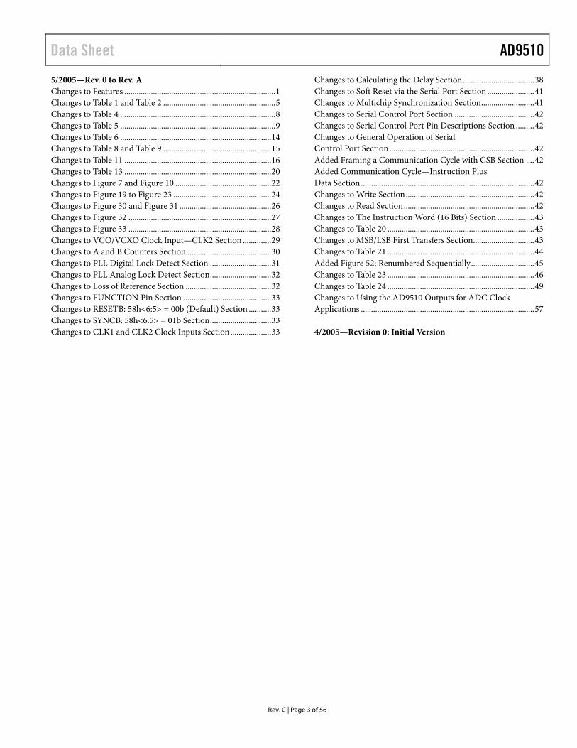
5/2005—Rev. 0 to Rev. A Changes to Features .......................................................................... 1 Changes to Table 1 and Table 2 ....................................................... 5 Changes to Table 4 ............................................................................ 8 Changes to Table 5 ............................................................................ 9 Changes to Table 6 .......................................................................... 14 Changes to Table 8 and Table 9 ..................................................... 15 Changes to Table 11 ........................................................................ 16 Changes to Table 13 ........................................................................ 20 Changes to Figure 7 and Figure 10 ............................................... 22 Changes to Figure 19 to Figure 23 ................................................ 24 Changes to Figure 30 and Figure 31 ............................................. 26 Changes to Figure 32 ...................................................................... 27 Changes to Figure 33 ...................................................................... 28 Changes to VCO/VCXO Clock Input—CLK2 Section .............. 29 Changes to A and B Counters Section ......................................... 30 Changes to PLL Digital Lock Detect Section .............................. 31 Changes to PLL Analog Lock Detect Section .............................. 32 Changes to Loss of Reference Section .......................................... 32 Changes to FUNCTION Pin Section ........................................... 33 Changes to RESETB: 58h<6:5> = 00b (Default) Section ........... 33 Changes to SYNCB: 58h<6:5> = 01b Section .............................. 33 Changes to CLK1 and CLK2 Clock Inputs Section .................... 33
Changes to Calculating the Delay Section ................................... 38 Changes to Soft Reset via the Serial Port Section ....................... 41 Changes to Multichip Synchronization Section .......................... 41 Changes to Serial Control Port Section ....................................... 42 Changes to Serial Control Port Pin Descriptions Section ......... 42 Changes to General Operation of Serial Control Port Section ....................................................................... 42 Added Framing a Communication Cycle with CSB Section .... 42 Added Communication Cycle—Instruction Plus Data Section ..................................................................................... 42 Changes to Write Section ............................................................... 42 Changes to Read Section ................................................................ 42 Changes to The Instruction Word (16 Bits) Section .................. 43 Changes to Table 20 ........................................................................ 43 Changes to MSB/LSB First Transfers Section.............................. 43 Changes to Table 21 ........................................................................ 44 Added Figure 52; Renumbered Sequentially ............................... 45 Changes to Table 23 ........................................................................ 46 Changes to Table 24 ........................................................................ 49 Changes to Using the AD9510 Outputs for ADC Clock Applications ..................................................................................... 57 4/2005—Revision 0: Initial Version
AD9510 Data Sheet
Rev. C | Page 4 of 56
SPECIFICATIONS Typical (typ) is given for VS = 3.3 V ± 5%, VS ≤ VCPS ≤ 5.5 V, TA = 25°C, RSET = 4.12 kΩ, CPRSET = 5.1 kΩ, unless otherwise noted. Minimum (min) and maximum (max) values are given over full VS and TA (−40°C to +85°C) variation.
PLL CHARACTERISTICS
Table 1. Parameter Min Typ Max Unit Test Conditions/Comments REFERENCE INPUTS (REFIN)
Input Frequency 0 250 MHz Input Sensitivity 150 mV p-p Self-Bias Voltage, REFIN 1.45 1.60 1.75 V Self-bias voltage of REFIN1 Self-Bias Voltage, REFINB 1.40 1.50 1.60 V Self-bias voltage of REFINB1 Input Resistance, REFIN 4.0 4.9 5.8 kΩ Self-biased1 Input Resistance, REFINB 4.5 5.4 6.3 kΩ Self-biased1 Input Capacitance 2 pF
PHASE FREQUENCY DETECTOR (PFD) PFD Input Frequency 100 MHz Antibacklash pulse width, Register 0x0D[1:0] = 00b PFD Input Frequency 100 MHz Antibacklash pulse width, Register 0x0D[1:0] = 01b PFD Input Frequency 45 MHz Antibacklash pulse width, Register 0x0D[1:0] = 10b Antibacklash Pulse Width 1.3 ns Register 0x0D[1:0] = 00b (this is the default setting) Antibacklash Pulse Width 2.9 ns Register 0x0D[1:0] = 01b Antibacklash Pulse Width 6.0 ns Register 0x0D[1:0] = 10b
CHARGE PUMP (CP) ICP Sink/Source Programmable
High Value 4.8 mA With CPRSET = 5.1 kΩ Low Value 0.60 mA Absolute Accuracy 2.5 % VCP = VCPS/2 CPRSET Range 2.7/10 kΩ
ICP Three-State Leakage 1 nA Sink-and-Source Current Matching 2 % 0.5 < VCP < VCPS − 0.5 V ICP vs. VCP 1.5 % 0.5 < VCP < VCPS − 0.5 V ICP vs. Temperature 2 % VCP = VCPS/2 V
RF CHARACTERISTICS (CLK2)2 Input Frequency 1.6 GHz Frequencies > 1200 MHz (LVPECL) or 800 MHz (LVDS)
require a minimum divide-by-2 (see the Distribution Section)
Input Sensitivity 150 mV p-p Input Common-Mode Voltage, VCM 1.5 1.6 1.7 V Self-biased, enables ac coupling Input Common-Mode Range, VCMR 1.3 1.8 V With 200 mV p-p signal applied Input Sensitivity, Single-Ended 150 mV p-p CLK2 ac-coupled, CLK2B capacitively bypassed to RF
ground Input Resistance 4.0 4.8 5.6 kΩ Self-biased Input Capacitance 2 pF
CLK2 VS. REFIN DELAY 500 ps Difference at PFD PRESCALER (PART OF N DIVIDER) See the VCO/VCXO Feedback Divider—N (P, A, B) section
Prescaler Input Frequency P = 2 DM (2/3) 600 MHz P = 4 DM (4/5) 1000 MHz P = 8 DM (8/9) 1600 MHz P = 16 DM (16/17) 1600 MHz P = 32 DM (32/33) 1600 MHz
CLK2 Input Frequency for PLL 300 MHz A, B counter input frequency
Data Sheet AD9510
Rev. C | Page 5 of 56
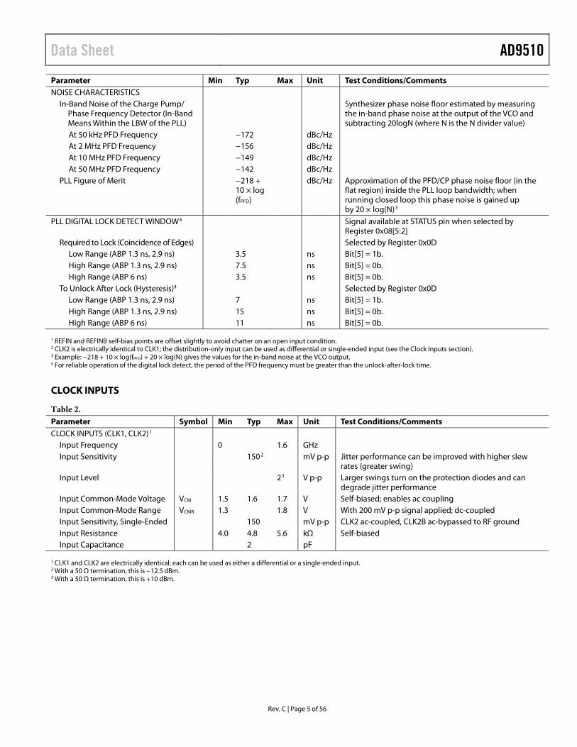
Parameter Min Typ Max Unit Test Conditions/Comments NOISE CHARACTERISTICS
In-Band Noise of the Charge Pump/ Phase Frequency Detector (In-Band Means Within the LBW of the PLL)
Synthesizer phase noise floor estimated by measuring the in-band phase noise at the output of the VCO and subtracting 20logN (where N is the N divider value)
At 50 kHz PFD Frequency −172 dBc/Hz At 2 MHz PFD Frequency −156 dBc/Hz At 10 MHz PFD Frequency −149 dBc/Hz At 50 MHz PFD Frequency −142 dBc/Hz
PLL Figure of Merit −218 + 10 × log (fPFD)
dBc/Hz Approximation of the PFD/CP phase noise floor (in the flat region) inside the PLL loop bandwidth; when running closed loop this phase noise is gained up by 20 × log(N)3
PLL DIGITAL LOCK DETECT WINDOW4 Signal available at STATUS pin when selected by Register 0x08[5:2]
Required to Lock (Coincidence of Edges) Selected by Register 0x0D Low Range (ABP 1.3 ns, 2.9 ns) 3.5 ns Bit[5] = 1b. High Range (ABP 1.3 ns, 2.9 ns) 7.5 ns Bit[5] = 0b. High Range (ABP 6 ns) 3.5 ns Bit[5] = 0b.
To Unlock After Lock (Hysteresis)4 Selected by Register 0x0D Low Range (ABP 1.3 ns, 2.9 ns) 7 ns Bit[5] = 1b. High Range (ABP 1.3 ns, 2.9 ns) 15 ns Bit[5] = 0b. High Range (ABP 6 ns) 11 ns Bit[5] = 0b.
1 REFIN and REFINB self-bias points are offset slightly to avoid chatter on an open input condition. 2 CLK2 is electrically identical to CLK1; the distribution-only input can be used as differential or single-ended input (see the Clock Inputs section). 3 Example: −218 + 10 × log(fPFD) + 20 × log(N) gives the values for the in-band noise at the VCO output. 4 For reliable operation of the digital lock detect, the period of the PFD frequency must be greater than the unlock-after-lock time.
CLOCK INPUTS
Table 2. Parameter Symbol Min Typ Max Unit Test Conditions/Comments CLOCK INPUTS (CLK1, CLK2)1
Input Frequency 0 1.6 GHz Input Sensitivity 1502 mV p-p Jitter performance can be improved with higher slew
rates (greater swing) Input Level 23 V p-p Larger swings turn on the protection diodes and can
degrade jitter performance Input Common-Mode Voltage VCM 1.5 1.6 1.7 V Self-biased; enables ac coupling Input Common-Mode Range VCMR 1.3 1.8 V With 200 mV p-p signal applied; dc-coupled Input Sensitivity, Single-Ended 150 mV p-p CLK2 ac-coupled, CLK2B ac-bypassed to RF ground Input Resistance 4.0 4.8 5.6 kΩ Self-biased Input Capacitance 2 pF
1 CLK1 and CLK2 are electrically identical; each can be used as either a differential or a single-ended input. 2 With a 50 Ω termination, this is −12.5 dBm. 3 With a 50 Ω termination, this is +10 dBm.
AD9510 Data Sheet
Rev. C | Page 6 of 56
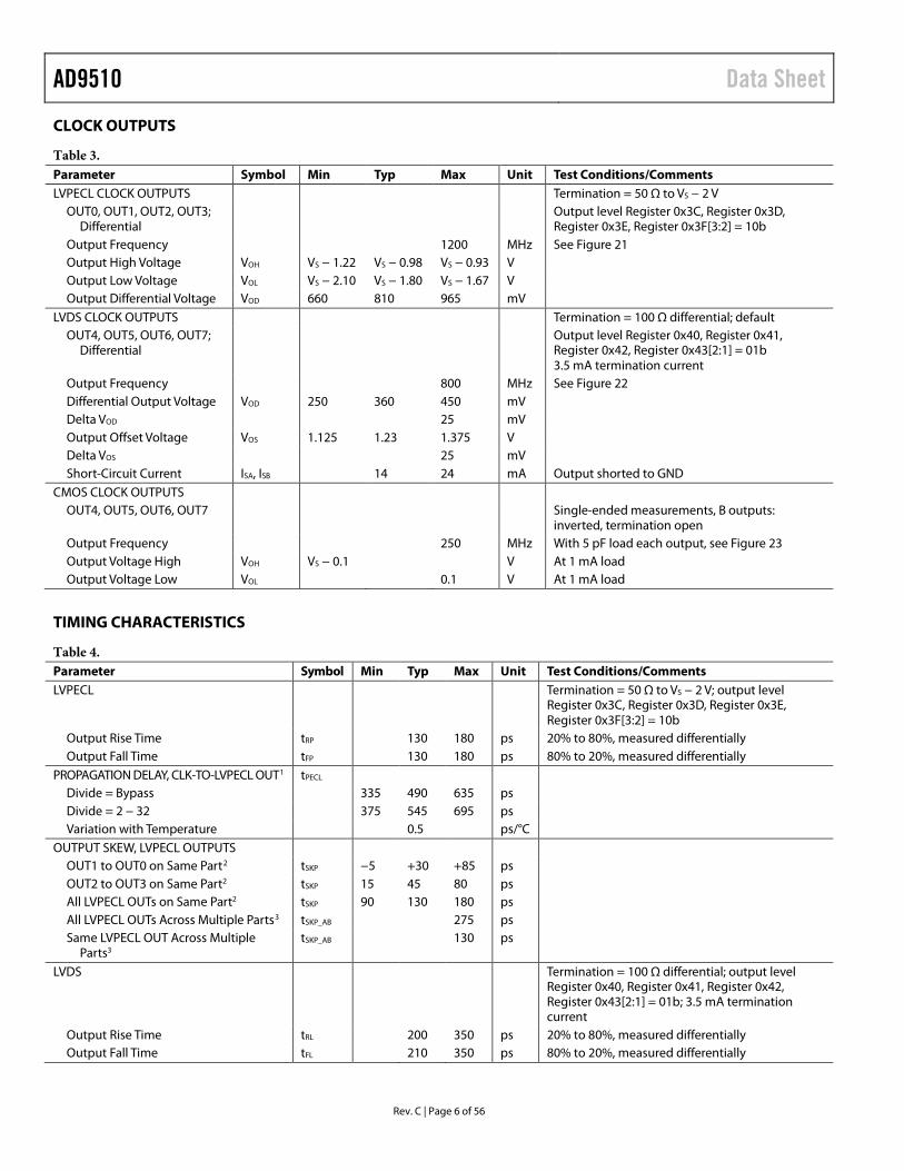
CLOCK OUTPUTS
Table 3. Parameter Symbol Min Typ Max Unit Test Conditions/Comments LVPECL CLOCK OUTPUTS Termination = 50 Ω to VS − 2 V
OUT0, OUT1, OUT2, OUT3; Differential
Output level Register 0x3C, Register 0x3D, Register 0x3E, Register 0x3F[3:2] = 10b
Output Frequency 1200 MHz See Figure 21 Output High Voltage VOH VS − 1.22 VS − 0.98 VS − 0.93 V Output Low Voltage VOL VS − 2.10 VS − 1.80 VS − 1.67 V Output Differential Voltage VOD 660 810 965 mV
LVDS CLOCK OUTPUTS Termination = 100 Ω differential; default OUT4, OUT5, OUT6, OUT7;
Differential Output level Register 0x40, Register 0x41,
Register 0x42, Register 0x43[2:1] = 01b 3.5 mA termination current
Output Frequency 800 MHz See Figure 22 Differential Output Voltage VOD 250 360 450 mV Delta VOD 25 mV Output Offset Voltage VOS 1.125 1.23 1.375 V Delta VOS 25 mV Short-Circuit Current ISA, ISB 14 24 mA Output shorted to GND
CMOS CLOCK OUTPUTS OUT4, OUT5, OUT6, OUT7 Single-ended measurements, B outputs:
inverted, termination open Output Frequency 250 MHz With 5 pF load each output, see Figure 23 Output Voltage High VOH VS − 0.1 V At 1 mA load Output Voltage Low VOL 0.1 V At 1 mA load
TIMING CHARACTERISTICS
Table 4. Parameter Symbol Min Typ Max Unit Test Conditions/Comments LVPECL Termination = 50 Ω to VS − 2 V; output level
Register 0x3C, Register 0x3D, Register 0x3E, Register 0x3F[3:2] = 10b
Output Rise Time tRP 130 180 ps 20% to 80%, measured differentially Output Fall Time tFP 130 180 ps 80% to 20%, measured differentially
PROPAGATION DELAY, CLK-TO-LVPECL OUT1 tPECL Divide = Bypass 335 490 635 ps Divide = 2 − 32 375 545 695 ps Variation with Temperature 0.5 ps/°C
OUTPUT SKEW, LVPECL OUTPUTS OUT1 to OUT0 on Same Part2 tSKP −5 +30 +85 ps OUT2 to OUT3 on Same Part2 tSKP 15 45 80 ps All LVPECL OUTs on Same Part2 tSKP 90 130 180 ps All LVPECL OUTs Across Multiple Parts3 tSKP_AB 275 ps Same LVPECL OUT Across Multiple
Parts3 tSKP_AB 130 ps
LVDS Termination = 100 Ω differential; output level Register 0x40, Register 0x41, Register 0x42, Register 0x43[2:1] = 01b; 3.5 mA termination current
Output Rise Time tRL 200 350 ps 20% to 80%, measured differentially Output Fall Time tFL 210 350 ps 80% to 20%, measured differentially
Data Sheet AD9510
Rev. C | Page 7 of 56
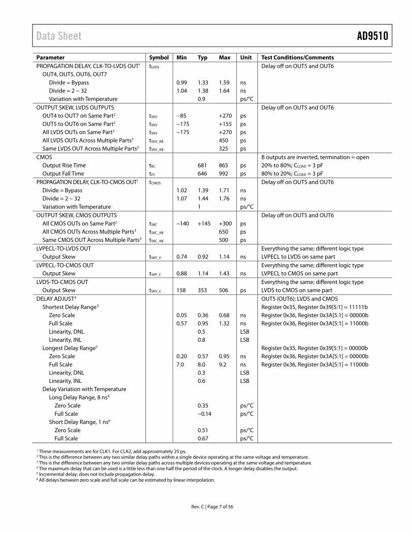
Parameter Symbol Min Typ Max Unit Test Conditions/Comments PROPAGATION DELAY, CLK-TO-LVDS OUT1 tLVDS Delay off on OUT5 and OUT6
OUT4, OUT5, OUT6, OUT7 Divide = Bypass 0.99 1.33 1.59 ns Divide = 2 − 32 1.04 1.38 1.64 ns Variation with Temperature 0.9 ps/°C
OUTPUT SKEW, LVDS OUTPUTS Delay off on OUT5 and OUT6 OUT4 to OUT7 on Same Part2 tSKV −85 +270 ps OUT5 to OUT6 on Same Part2 tSKV −175 +155 ps All LVDS OUTs on Same Part2 tSKV −175 +270 ps All LVDS OUTs Across Multiple Parts3 tSKV_AB 450 ps Same LVDS OUT Across Multiple Parts3 tSKV_AB 325 ps
CMOS B outputs are inverted, termination = open Output Rise Time tRC 681 865 ps 20% to 80%; CLOAD = 3 pF Output Fall Time tFC 646 992 ps 80% to 20%; CLOAD = 3 pF
PROPAGATION DELAY, CLK-TO-CMOS OUT1 tCMOS Delay off on OUT5 and OUT6 Divide = Bypass 1.02 1.39 1.71 ns Divide = 2 − 32 1.07 1.44 1.76 ns Variation with Temperature 1 ps/°C
OUTPUT SKEW, CMOS OUTPUTS Delay off on OUT5 and OUT6 All CMOS OUTs on Same Part2 tSKC −140 +145 +300 ps All CMOS OUTs Across Multiple Parts3 tSKC_AB 650 ps Same CMOS OUT Across Multiple Parts3 tSKC_AB 500 ps
LVPECL-TO-LVDS OUT Everything the same; different logic type Output Skew tSKP_V 0.74 0.92 1.14 ns LVPECL to LVDS on same part
LVPECL-TO-CMOS OUT Everything the same; different logic type Output Skew tSKP_C 0.88 1.14 1.43 ns LVPECL to CMOS on same part
LVDS-TO-CMOS OUT Everything the same; different logic type Output Skew tSKV_C 158 353 506 ps LVDS to CMOS on same part
DELAY ADJUST4 OUT5 (OUT6); LVDS and CMOS Shortest Delay Range5 Register 0x35, Register 0x39[5:1] = 11111b
Zero Scale 0.05 0.36 0.68 ns Register 0x36, Register 0x3A[5:1] = 00000b Full Scale 0.57 0.95 1.32 ns Register 0x36, Register 0x3A[5:1] = 11000b Linearity, DNL 0.5 LSB Linearity, INL 0.8 LSB
Longest Delay Range5 Register 0x35, Register 0x39[5:1] = 00000b Zero Scale 0.20 0.57 0.95 ns Register 0x36, Register 0x3A[5:1] = 00000b Full Scale 7.0 8.0 9.2 ns Register 0x36, Register 0x3A[5:1] = 11000b Linearity, DNL 0.3 LSB Linearity, INL 0.6 LSB
Delay Variation with Temperature Long Delay Range, 8 ns6
Zero Scale 0.35 ps/°C Full Scale −0.14 ps/°C
Short Delay Range, 1 ns6 Zero Scale 0.51 ps/°C Full Scale 0.67 ps/°C
1 These measurements are for CLK1. For CLK2, add approximately 25 ps. 2 This is the difference between any two similar delay paths within a single device operating at the same voltage and temperature. 3 This is the difference between any two similar delay paths across multiple devices operating at the same voltage and temperature. 4 The maximum delay that can be used is a little less than one half the period of the clock. A longer delay disables the output. 5 Incremental delay; does not include propagation delay. 6 All delays between zero scale and full scale can be estimated by linear interpolation.
AD9510 Data Sheet
Rev. C | Page 8 of 56
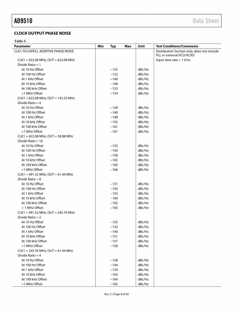
CLOCK OUTPUT PHASE NOISE
Table 5. Parameter Min Typ Max Unit Test Conditions/Comments CLK1-TO-LVPECL ADDITIVE PHASE NOISE Distribution Section only, does not include
PLL or external VCO/VCXO CLK1 = 622.08 MHz, OUT = 622.08 MHz Input slew rate > 1 V/ns Divide Ratio = 1
At 10 Hz Offset −125 dBc/Hz At 100 Hz Offset −132 dBc/Hz At 1 kHz Offset −140 dBc/Hz At 10 kHz Offset −148 dBc/Hz At 100 kHz Offset −153 dBc/Hz >1 MHz Offset −154 dBc/Hz
CLK1 = 622.08 MHz, OUT = 155.52 MHz Divide Ratio = 4
At 10 Hz Offset −128 dBc/Hz At 100 Hz Offset −140 dBc/Hz At 1 kHz Offset −148 dBc/Hz At 10 kHz Offset −155 dBc/Hz At 100 kHz Offset −161 dBc/Hz >1 MHz Offset −161 dBc/Hz
CLK1 = 622.08 MHz, OUT = 38.88 MHz Divide Ratio = 16
At 10 Hz Offset −135 dBc/Hz At 100 Hz Offset −145 dBc/Hz At 1 kHz Offset −158 dBc/Hz At 10 kHz Offset −165 dBc/Hz At 100 kHz Offset −165 dBc/Hz >1 MHz Offset −166 dBc/Hz
CLK1 = 491.52 MHz, OUT = 61.44 MHz Divide Ratio = 8
At 10 Hz Offset −131 dBc/Hz At 100 Hz Offset −142 dBc/Hz At 1 kHz Offset −153 dBc/Hz At 10 kHz Offset −160 dBc/Hz At 100 kHz Offset −165 dBc/Hz > 1 MHz Offset −165 dBc/Hz
CLK1 = 491.52 MHz, OUT = 245.76 MHz Divide Ratio = 2
At 10 Hz Offset −125 dBc/Hz At 100 Hz Offset −132 dBc/Hz At 1 kHz Offset −140 dBc/Hz At 10 kHz Offset −151 dBc/Hz At 100 kHz Offset −157 dBc/Hz >1 MHz Offset −158 dBc/Hz
CLK1 = 245.76 MHz, OUT = 61.44 MHz Divide Ratio = 4
At 10 Hz Offset −138 dBc/Hz At 100 Hz Offset −144 dBc/Hz At 1 kHz Offset −154 dBc/Hz At 10 kHz Offset −163 dBc/Hz At 100 kHz Offset −164 dBc/Hz >1 MHz Offset −165 dBc/Hz

Data Sheet AD9510
Rev. C | Page 9 of 56
Parameter Min Typ Max Unit Test Conditions/Comments CLK1-TO-LVDS ADDITIVE PHASE NOISE Distribution Section only; does not include
PLL or external VCO/VCXO CLK1 = 622.08 MHz, OUT= 622.08 MHz Divide Ratio = 1
At 10 Hz Offset −100 dBc/Hz At 100 Hz Offset −110 dBc/Hz At 1 kHz Offset −118 dBc/Hz At 10 kHz Offset −129 dBc/Hz At 100 kHz Offset −135 dBc/Hz At 1 MHz Offset −140 dBc/Hz >10 MHz Offset −148 dBc/Hz
CLK1 = 622.08 MHz, OUT = 155.52 MHz Divide Ratio = 4
At 10 Hz Offset −112 dBc/Hz At 100 Hz Offset −122 dBc/Hz At 1 kHz Offset −132 dBc/Hz At 10 kHz Offset −142 dBc/Hz At 100 kHz Offset −148 dBc/Hz At 1 MHz Offset −152 dBc/Hz >10 MHz Offset −155 dBc/Hz
CLK1 = 491.52 MHz, OUT = 245.76 MHz Divide Ratio = 2
At 10 Hz Offset −108 dBc/Hz At 100 Hz Offset −118 dBc/Hz At 1 kHz Offset −128 dBc/Hz At 10 kHz Offset −138 dBc/Hz At 100 kHz Offset −145 dBc/Hz At 1 MHz Offset −148 dBc/Hz >10 MHz Offset −154 dBc/Hz
CLK1 = 491.52 MHz, OUT = 122.88 MHz Divide Ratio = 4
At 10 Hz Offset −118 dBc/Hz At 100 Hz Offset −129 dBc/Hz At 1 kHz Offset −136 dBc/Hz At 10 kHz Offset −147 dBc/Hz At 100 kHz Offset −153 dBc/Hz At 1 MHz Offset −156 dBc/Hz >10 MHz Offset −158 dBc/Hz
CLK1 = 245.76 MHz, OUT = 245.76 MHz Divide Ratio = 1
At 10 Hz Offset −108 dBc/Hz At 100 Hz Offset −118 dBc/Hz At 1 kHz Offset −128 dBc/Hz At 10 kHz Offset −138 dBc/Hz At 100 kHz Offset −145 dBc/Hz At 1 MHz Offset −148 dBc/Hz >10 MHz Offset −155 dBc/Hz
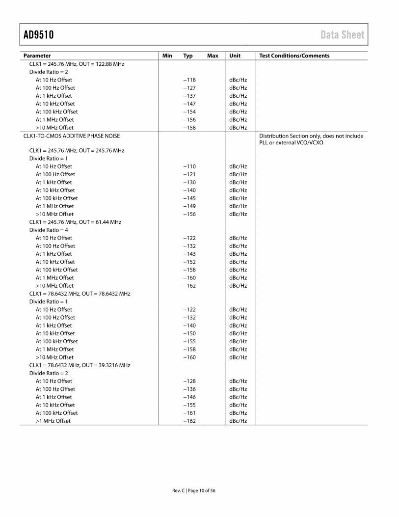
AD9510 Data Sheet
Rev. C | Page 10 of 56
Parameter Min Typ Max Unit Test Conditions/Comments CLK1 = 245.76 MHz, OUT = 122.88 MHz Divide Ratio = 2
At 10 Hz Offset −118 dBc/Hz At 100 Hz Offset −127 dBc/Hz At 1 kHz Offset −137 dBc/Hz At 10 kHz Offset −147 dBc/Hz At 100 kHz Offset −154 dBc/Hz At 1 MHz Offset −156 dBc/Hz >10 MHz Offset −158 dBc/Hz
CLK1-TO-CMOS ADDITIVE PHASE NOISE Distribution Section only, does not include PLL or external VCO/VCXO
CLK1 = 245.76 MHz, OUT = 245.76 MHz Divide Ratio = 1
At 10 Hz Offset −110 dBc/Hz At 100 Hz Offset −121 dBc/Hz At 1 kHz Offset −130 dBc/Hz At 10 kHz Offset −140 dBc/Hz At 100 kHz Offset −145 dBc/Hz At 1 MHz Offset −149 dBc/Hz >10 MHz Offset −156 dBc/Hz
CLK1 = 245.76 MHz, OUT = 61.44 MHz Divide Ratio = 4
At 10 Hz Offset −122 dBc/Hz At 100 Hz Offset −132 dBc/Hz At 1 kHz Offset −143 dBc/Hz At 10 kHz Offset −152 dBc/Hz At 100 kHz Offset −158 dBc/Hz At 1 MHz Offset −160 dBc/Hz >10 MHz Offset −162 dBc/Hz
CLK1 = 78.6432 MHz, OUT = 78.6432 MHz Divide Ratio = 1
At 10 Hz Offset −122 dBc/Hz At 100 Hz Offset −132 dBc/Hz At 1 kHz Offset −140 dBc/Hz At 10 kHz Offset −150 dBc/Hz At 100 kHz Offset −155 dBc/Hz At 1 MHz Offset −158 dBc/Hz >10 MHz Offset −160 dBc/Hz
CLK1 = 78.6432 MHz, OUT = 39.3216 MHz Divide Ratio = 2
At 10 Hz Offset −128 dBc/Hz At 100 Hz Offset −136 dBc/Hz At 1 kHz Offset −146 dBc/Hz At 10 kHz Offset −155 dBc/Hz At 100 kHz Offset −161 dBc/Hz >1 MHz Offset −162 dBc/Hz
Data Sheet AD9510
Rev. C | Page 11 of 56
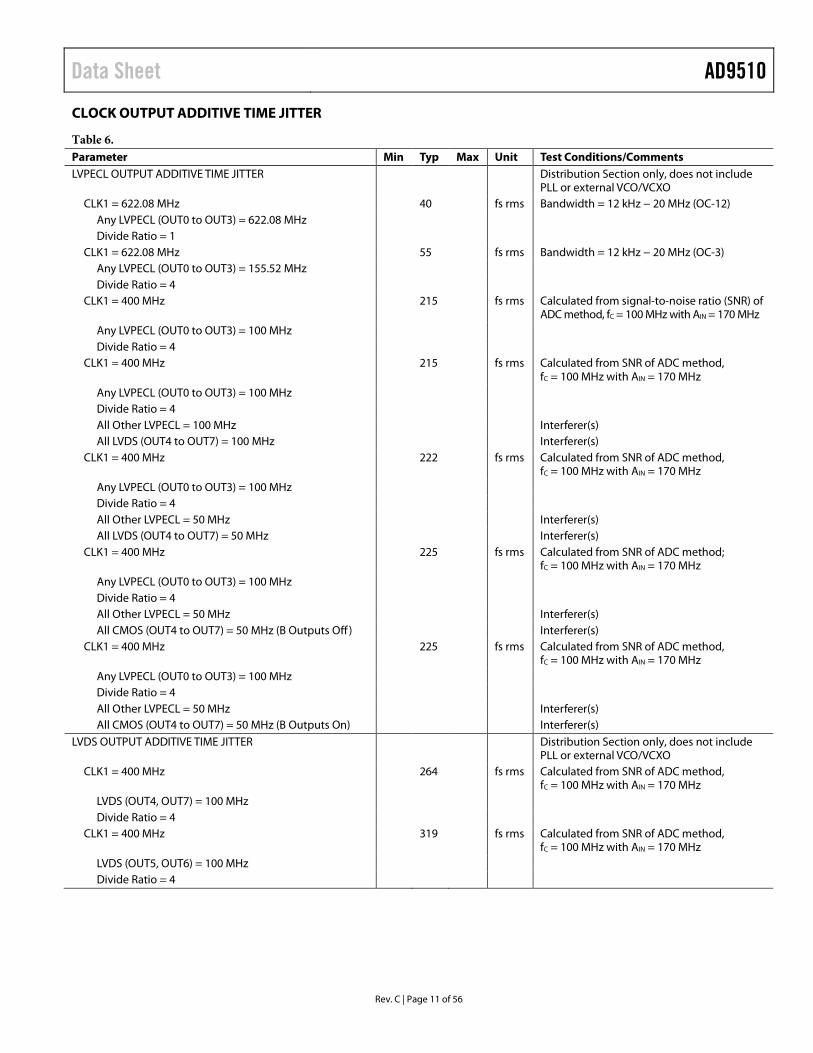
CLOCK OUTPUT ADDITIVE TIME JITTER
Table 6. Parameter Min Typ Max Unit Test Conditions/Comments LVPECL OUTPUT ADDITIVE TIME JITTER Distribution Section only, does not include
PLL or external VCO/VCXO CLK1 = 622.08 MHz 40 fs rms Bandwidth = 12 kHz − 20 MHz (OC-12)
Any LVPECL (OUT0 to OUT3) = 622.08 MHz Divide Ratio = 1
CLK1 = 622.08 MHz 55 fs rms Bandwidth = 12 kHz − 20 MHz (OC-3) Any LVPECL (OUT0 to OUT3) = 155.52 MHz Divide Ratio = 4
CLK1 = 400 MHz 215 fs rms Calculated from signal-to-noise ratio (SNR) of ADC method, fC = 100 MHz with AIN = 170 MHz
Any LVPECL (OUT0 to OUT3) = 100 MHz Divide Ratio = 4
CLK1 = 400 MHz 215 fs rms Calculated from SNR of ADC method, fC = 100 MHz with AIN = 170 MHz
Any LVPECL (OUT0 to OUT3) = 100 MHz Divide Ratio = 4 All Other LVPECL = 100 MHz Interferer(s) All LVDS (OUT4 to OUT7) = 100 MHz Interferer(s)
CLK1 = 400 MHz 222 fs rms Calculated from SNR of ADC method, fC = 100 MHz with AIN = 170 MHz
Any LVPECL (OUT0 to OUT3) = 100 MHz Divide Ratio = 4 All Other LVPECL = 50 MHz Interferer(s) All LVDS (OUT4 to OUT7) = 50 MHz Interferer(s)
CLK1 = 400 MHz 225 fs rms Calculated from SNR of ADC method; fC = 100 MHz with AIN = 170 MHz
Any LVPECL (OUT0 to OUT3) = 100 MHz Divide Ratio = 4 All Other LVPECL = 50 MHz Interferer(s) All CMOS (OUT4 to OUT7) = 50 MHz (B Outputs Off ) Interferer(s)
CLK1 = 400 MHz 225 fs rms Calculated from SNR of ADC method, fC = 100 MHz with AIN = 170 MHz
Any LVPECL (OUT0 to OUT3) = 100 MHz Divide Ratio = 4 All Other LVPECL = 50 MHz Interferer(s) All CMOS (OUT4 to OUT7) = 50 MHz (B Outputs On) Interferer(s)
LVDS OUTPUT ADDITIVE TIME JITTER Distribution Section only, does not include PLL or external VCO/VCXO
CLK1 = 400 MHz 264 fs rms Calculated from SNR of ADC method, fC = 100 MHz with AIN = 170 MHz
LVDS (OUT4, OUT7) = 100 MHz Divide Ratio = 4
CLK1 = 400 MHz 319 fs rms Calculated from SNR of ADC method, fC = 100 MHz with AIN = 170 MHz
LVDS (OUT5, OUT6) = 100 MHz Divide Ratio = 4
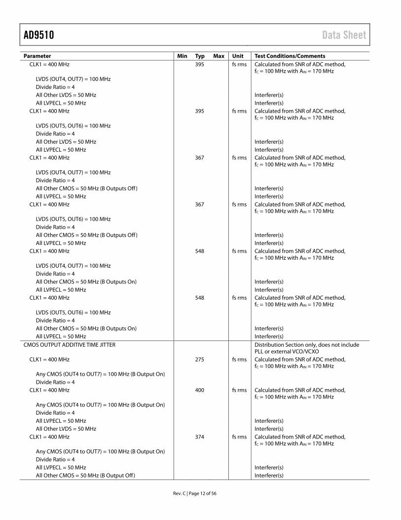
AD9510 Data Sheet
Rev. C | Page 12 of 56
Parameter Min Typ Max Unit Test Conditions/Comments CLK1 = 400 MHz 395 fs rms Calculated from SNR of ADC method,
fC = 100 MHz with AIN = 170 MHz LVDS (OUT4, OUT7) = 100 MHz Divide Ratio = 4 All Other LVDS = 50 MHz Interferer(s) All LVPECL = 50 MHz Interferer(s)
CLK1 = 400 MHz 395 fs rms Calculated from SNR of ADC method, fC = 100 MHz with AIN = 170 MHz
LVDS (OUT5, OUT6) = 100 MHz Divide Ratio = 4 All Other LVDS = 50 MHz Interferer(s) All LVPECL = 50 MHz Interferer(s)
CLK1 = 400 MHz 367 fs rms Calculated from SNR of ADC method, fC = 100 MHz with AIN = 170 MHz
LVDS (OUT4, OUT7) = 100 MHz Divide Ratio = 4 All Other CMOS = 50 MHz (B Outputs Off ) Interferer(s) All LVPECL = 50 MHz Interferer(s)
CLK1 = 400 MHz 367 fs rms Calculated from SNR of ADC method, fC = 100 MHz with AIN = 170 MHz
LVDS (OUT5, OUT6) = 100 MHz Divide Ratio = 4 All Other CMOS = 50 MHz (B Outputs Off ) Interferer(s) All LVPECL = 50 MHz Interferer(s)
CLK1 = 400 MHz 548 fs rms Calculated from SNR of ADC method, fC = 100 MHz with AIN = 170 MHz
LVDS (OUT4, OUT7) = 100 MHz Divide Ratio = 4 All Other CMOS = 50 MHz (B Outputs On) Interferer(s) All LVPECL = 50 MHz Interferer(s)
CLK1 = 400 MHz 548 fs rms Calculated from SNR of ADC method, fC = 100 MHz with AIN = 170 MHz
LVDS (OUT5, OUT6) = 100 MHz Divide Ratio = 4 All Other CMOS = 50 MHz (B Outputs On) Interferer(s) All LVPECL = 50 MHz Interferer(s)
CMOS OUTPUT ADDITIVE TIME JITTER Distribution Section only, does not include PLL or external VCO/VCXO
CLK1 = 400 MHz 275 fs rms Calculated from SNR of ADC method, fC = 100 MHz with AIN = 170 MHz
Any CMOS (OUT4 to OUT7) = 100 MHz (B Output On) Divide Ratio = 4
CLK1 = 400 MHz 400 fs rms Calculated from SNR of ADC method, fC = 100 MHz with AIN = 170 MHz
Any CMOS (OUT4 to OUT7) = 100 MHz (B Output On) Divide Ratio = 4 All LVPECL = 50 MHz Interferer(s) All Other LVDS = 50 MHz Interferer(s)
CLK1 = 400 MHz 374 fs rms Calculated from SNR of ADC method, fC = 100 MHz with AIN = 170 MHz
Any CMOS (OUT4 to OUT7) = 100 MHz (B Output On) Divide Ratio = 4 All LVPECL = 50 MHz Interferer(s) All Other CMOS = 50 MHz (B Output Off ) Interferer(s)
Data Sheet AD9510
Rev. C | Page 13 of 56
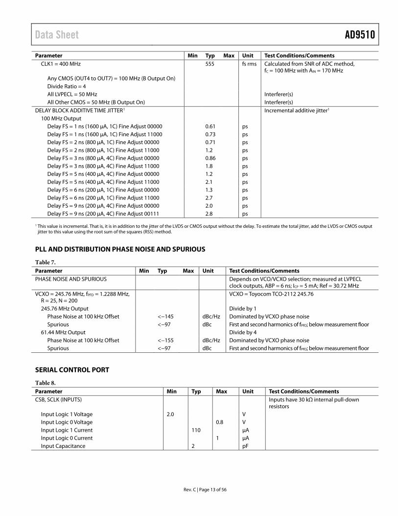
Parameter Min Typ Max Unit Test Conditions/Comments CLK1 = 400 MHz 555 fs rms Calculated from SNR of ADC method,
fC = 100 MHz with AIN = 170 MHz Any CMOS (OUT4 to OUT7) = 100 MHz (B Output On) Divide Ratio = 4 All LVPECL = 50 MHz Interferer(s) All Other CMOS = 50 MHz (B Output On) Interferer(s)
DELAY BLOCK ADDITIVE TIME JITTER1 Incremental additive jitter1 100 MHz Output
Delay FS = 1 ns (1600 μA, 1C) Fine Adjust 00000 0.61 ps Delay FS = 1 ns (1600 μA, 1C) Fine Adjust 11000 0.73 ps Delay FS = 2 ns (800 μA, 1C) Fine Adjust 00000 0.71 ps Delay FS = 2 ns (800 μA, 1C) Fine Adjust 11000 1.2 ps Delay FS = 3 ns (800 μA, 4C) Fine Adjust 00000 0.86 ps Delay FS = 3 ns (800 μA, 4C) Fine Adjust 11000 1.8 ps Delay FS = 5 ns (400 μA, 4C) Fine Adjust 00000 1.2 ps Delay FS = 5 ns (400 μA, 4C) Fine Adjust 11000 2.1 ps Delay FS = 6 ns (200 μA, 1C) Fine Adjust 00000 1.3 ps Delay FS = 6 ns (200 μA, 1C) Fine Adjust 11000 2.7 ps Delay FS = 9 ns (200 μA, 4C) Fine Adjust 00000 2.0 ps Delay FS = 9 ns (200 μA, 4C) Fine Adjust 00111 2.8 ps
1 This value is incremental. That is, it is in addition to the jitter of the LVDS or CMOS output without the delay. To estimate the total jitter, add the LVDS or CMOS output
jitter to this value using the root sum of the squares (RSS) method.
PLL AND DISTRIBUTION PHASE NOISE AND SPURIOUS
Table 7. Parameter Min Typ Max Unit Test Conditions/Comments PHASE NOISE AND SPURIOUS Depends on VCO/VCXO selection; measured at LVPECL
clock outputs, ABP = 6 ns; ICP = 5 mA; Ref = 30.72 MHz VCXO = 245.76 MHz, fPFD = 1.2288 MHz,
R = 25, N = 200 VCXO = Toyocom TCO-2112 245.76
245.76 MHz Output Divide by 1 Phase Noise at 100 kHz Offset <−145 dBc/Hz Dominated by VCXO phase noise Spurious <−97 dBc First and second harmonics of fPFD; below measurement floor
61.44 MHz Output Divide by 4 Phase Noise at 100 kHz Offset <−155 dBc/Hz Dominated by VCXO phase noise Spurious <−97 dBc First and second harmonics of fPFD; below measurement floor
SERIAL CONTROL PORT
Table 8. Parameter Min Typ Max Unit Test Conditions/Comments CSB, SCLK (INPUTS) Inputs have 30 kΩ internal pull-down
resistors Input Logic 1 Voltage 2.0 V Input Logic 0 Voltage 0.8 V Input Logic 1 Current 110 µA Input Logic 0 Current 1 µA Input Capacitance 2 pF
AD9510 Data Sheet
Rev. C | Page 14 of 56
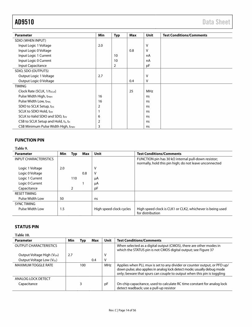
Parameter Min Typ Max Unit Test Conditions/Comments SDIO (WHEN INPUT)
Input Logic 1 Voltage 2.0 V Input Logic 0 Voltage 0.8 V Input Logic 1 Current 10 nA Input Logic 0 Current 10 nA Input Capacitance 2 pF
SDIO, SDO (OUTPUTS) Output Logic 1 Voltage 2.7 V Output Logic 0 Voltage 0.4 V
TIMING Clock Rate (SCLK, 1/tSCLK) 25 MHz Pulse Width High, tPWH 16 ns Pulse Width Low, tPWL 16 ns SDIO to SCLK Setup, tDS 2 ns SCLK to SDIO Hold, tDH 1 ns SCLK to Valid SDIO and SDO, tDV 6 ns CSB to SCLK Setup and Hold, tS, tH 2 ns CSB Minimum Pulse Width High, tPWH 3 ns
FUNCTION PIN
Table 9. Parameter Min Typ Max Unit Test Conditions/Comments INPUT CHARACTERISTICS FUNCTION pin has 30 kΩ internal pull-down resistor;
normally, hold this pin high; do not leave unconnected Logic 1 Voltage 2.0 V Logic 0 Voltage 0.8 V Logic 1 Current 110 µA Logic 0 Current 1 µA Capacitance 2 pF
RESET TIMING Pulse Width Low 50 ns
SYNC TIMING Pulse Width Low 1.5 High speed clock cycles High speed clock is CLK1 or CLK2, whichever is being used
for distribution
STATUS PIN
Table 10. Parameter Min Typ Max Unit Test Conditions/Comments OUTPUT CHARACTERISTICS When selected as a digital output (CMOS), there are other modes in
which the STATUS pin is not CMOS digital output; see Figure 37 Output Voltage High (VOH) 2.7 V Output Voltage Low (VOL) 0.4 V
MAXIMUM TOGGLE RATE 100 MHz Applies when PLL mux is set to any divider or counter output, or PFD up/ down pulse; also applies in analog lock detect mode; usually debug mode only; beware that spurs can couple to output when this pin is toggling
ANALOG LOCK DETECT Capacitance 3 pF On-chip capacitance, used to calculate RC time constant for analog lock
detect readback; use a pull-up resistor
Data Sheet AD9510
Rev. C | Page 15 of 56
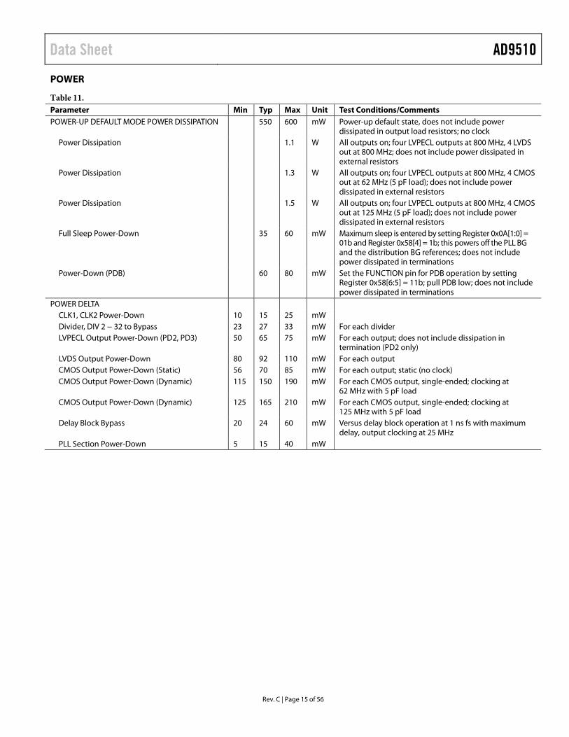
POWER
Table 11. Parameter Min Typ Max Unit Test Conditions/Comments POWER-UP DEFAULT MODE POWER DISSIPATION 550 600 mW Power-up default state, does not include power
dissipated in output load resistors; no clock Power Dissipation 1.1 W All outputs on; four LVPECL outputs at 800 MHz, 4 LVDS
out at 800 MHz; does not include power dissipated in external resistors
Power Dissipation 1.3 W All outputs on; four LVPECL outputs at 800 MHz, 4 CMOS out at 62 MHz (5 pF load); does not include power dissipated in external resistors
Power Dissipation 1.5 W All outputs on; four LVPECL outputs at 800 MHz, 4 CMOS out at 125 MHz (5 pF load); does not include power dissipated in external resistors
Full Sleep Power-Down 35 60 mW Maximum sleep is entered by setting Register 0x0A[1:0] = 01b and Register 0x58[4] = 1b; this powers off the PLL BG and the distribution BG references; does not include power dissipated in terminations
Power-Down (PDB) 60 80 mW Set the FUNCTION pin for PDB operation by setting Register 0x58[6:5] = 11b; pull PDB low; does not include power dissipated in terminations
POWER DELTA CLK1, CLK2 Power-Down 10 15 25 mW Divider, DIV 2 − 32 to Bypass 23 27 33 mW For each divider LVPECL Output Power-Down (PD2, PD3) 50 65 75 mW For each output; does not include dissipation in
termination (PD2 only) LVDS Output Power-Down 80 92 110 mW For each output CMOS Output Power-Down (Static) 56 70 85 mW For each output; static (no clock) CMOS Output Power-Down (Dynamic) 115 150 190 mW For each CMOS output, single-ended; clocking at
62 MHz with 5 pF load CMOS Output Power-Down (Dynamic) 125 165 210 mW For each CMOS output, single-ended; clocking at
125 MHz with 5 pF load Delay Block Bypass 20 24 60 mW Versus delay block operation at 1 ns fs with maximum
delay, output clocking at 25 MHz PLL Section Power-Down 5 15 40 mW
AD9510 Data Sheet
Rev. C | Page 16 of 56
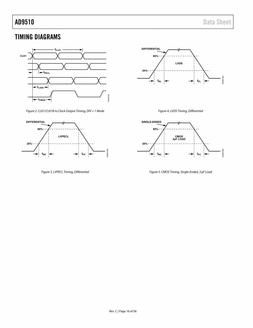
TIMING DIAGRAMS
Figure 2. CLK1/CLK1B to Clock Output Timing, DIV = 1 Mode
Figure 3. LVPECL Timing, Differential
Figure 4. LVDS Timing, Differential
Figure 5. CMOS Timing, Single-Ended, 3 pF Load
0504
6-00
2
CLK1
tCMOS
tCLK1
tLVDS
tPECL
0504
6-06
4
DIFFERENTIAL
LVPECL
80%
20%
tRP tFP
0504
6-06
5
DIFFERENTIAL
LVDS
80%
20%
tRL tFL
0504
6-06
6
SINGLE-ENDED
CMOS3pF LOAD
80%
20%
tRC tFC
Data Sheet AD9510
Rev. C | Page 17 of 56
ABSOLUTE MAXIMUM RATINGS Table 12. Parameter Value VS to GND −0.3 V to +3.6 V VCP to GND −0.3 V to +5.8 V VCP to VS −0.3 V to +5.8 V REFIN, REFINB to GND −0.3 V to VS + 0.3 V RSET to GND −0.3 V to VS + 0.3 V CPRSET to GND −0.3 V to VS + 0.3 V CLK1, CLK1B, CLK2, CLK2B to GND −0.3 V to VS + 0.3 V CLK1 to CLK1B −1.2 V to +1.2 V CLK2 to CLK2B −1.2 V to +1.2 V SCLK, SDIO, SDO, CSB to GND −0.3 V to VS + 0.3 V OUT0, OUT1, OUT2, OUT3 to GND −0.3 V to VS + 0.3 V OUT4, OUT5, OUT6, OUT7 to GND −0.3 V to VS + 0.3 V FUNCTION to GND −0.3 V to VS + 0.3 V STATUS to GND −0.3 V to VS + 0.3 V Junction Temperature1 150°C Storage Temperature −65°C to +150°C Lead Temperature (10 sec) 300°C 1 See Thermal Characteristics for θJA
Stresses at or above those listed under Absolute Maximum Ratings may cause permanent damage to the product. This is a stress rating only; functional operation of the product at these or any other conditions above those indicated in the operational section of this specification is not implied. Operation beyond the maximum operating conditions for extended periods may affect product reliability.
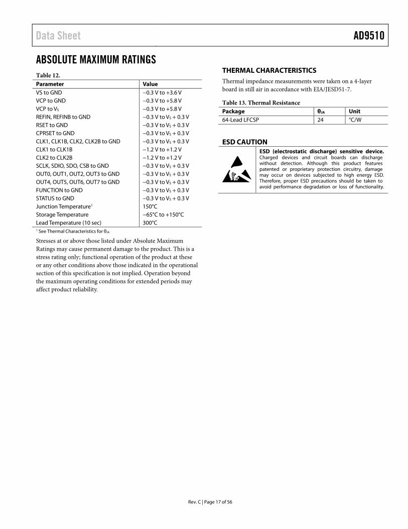
THERMAL CHARACTERISTICS Thermal impedance measurements were taken on a 4-layer board in still air in accordance with EIA/JESD51-7.
Table 13. Thermal Resistance Package θJA Unit 64-Lead LFCSP 24 °C/W
ESD CAUTION
AD9510 Data Sheet
Rev. C | Page 18 of 56
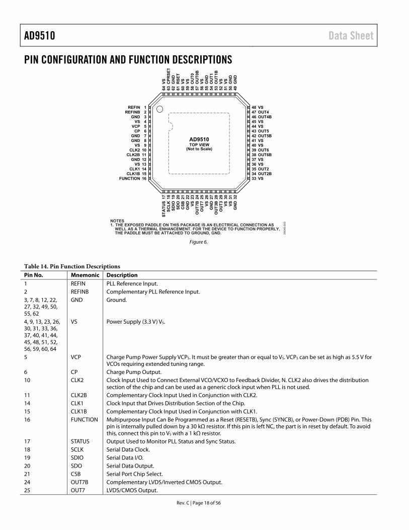
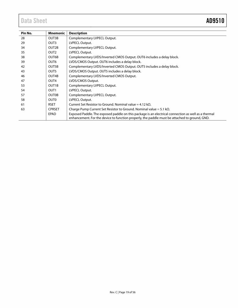
PIN CONFIGURATION AND FUNCTION DESCRIPTIONS
Figure 6.
Table 14. Pin Function Descriptions Pin No. Mnemonic Description 1 REFIN PLL Reference Input. 2 REFINB Complementary PLL Reference Input. 3, 7, 8, 12, 22, 27, 32, 49, 50, 55, 62
GND Ground.
4, 9, 13, 23, 26, 30, 31, 33, 36, 37, 40, 41, 44, 45, 48, 51, 52, 56, 59, 60, 64
VS Power Supply (3.3 V) VS.
5 VCP Charge Pump Power Supply VCPS. It must be greater than or equal to VS. VCPS can be set as high as 5.5 V for VCOs requiring extended tuning range.
6 CP Charge Pump Output. 10 CLK2 Clock Input Used to Connect External VCO/VCXO to Feedback Divider, N. CLK2 also drives the distribution
section of the chip and can be used as a generic clock input when PLL is not used. 11 CLK2B Complementary Clock Input Used in Conjunction with CLK2. 14 CLK1 Clock Input that Drives Distribution Section of the Chip. 15 CLK1B Complementary Clock Input Used in Conjunction with CLK1. 16 FUNCTION Multipurpose Input Can Be Programmed as a Reset (RESETB), Sync (SYNCB), or Power-Down (PDB) Pin. This
pin is internally pulled down by a 30 kΩ resistor. If this pin is left NC, the part is in reset by default. To avoid this, connect this pin to VS with a 1 kΩ resistor.
17 STATUS Output Used to Monitor PLL Status and Sync Status. 18 SCLK Serial Data Clock. 19 SDIO Serial Data I/O. 20 SDO Serial Data Output. 21 CSB Serial Port Chip Select. 24 OUT7B Complementary LVDS/Inverted CMOS Output. 25 OUT7 LVDS/CMOS Output.
0504
6-00
3NOTES1. THE EXPOSED PADDLE ON THIS PACKAGE IS AN ELECTRICAL CONNECTION AS
WELL AS A THERMAL ENHANCEMENT. FOR THE DEVICE TO FUNCTION PROPERLY,THE PADDLE MUST BE ATTACHED TO GROUND, GND.
17 18 19 20 21 22 23 24 25 26 27 28 29 30 31 32
STA
TUS
SCLK
SDIO
SDO
CSB
GN
D VSO
UT7
BO
UT7 VS
GN
DO
UT3
BO
UT3 VS VS
GN
D
64 63 62 61 60 59 58 57 56 55 54 53 52 51 50 49
VS CPR
SET
GN
DR
SET
VS VS OU
T0O
UT0
BVS G
ND
OU
T1O
UT1
BVS VS G
ND
GN
D
123456789
10111213141516
REFINREFINB
GNDVS
VCPCP
GNDGND
VSCLK2
CLK2BGND
VSCLK1
CLK1BFUNCTION
VSOUT4OUT4BVSVSOUT5OUT5BVSVSOUT6OUT6BVSVSOUT2OUT2BVS
48474645444342414039383736353433
AD9510TOP VIEW
(Not to Scale)
Data Sheet AD9510
Rev. C | Page 19 of 56
Pin No. Mnemonic Description 28 OUT3B Complementary LVPECL Output. 29 OUT3 LVPECL Output. 34 OUT2B Complementary LVPECL Output. 35 OUT2 LVPECL Output. 38 OUT6B Complementary LVDS/Inverted CMOS Output. OUT6 includes a delay block. 39 OUT6 LVDS/CMOS Output. OUT6 includes a delay block. 42 OUT5B Complementary LVDS/Inverted CMOS Output. OUT5 includes a delay block. 43 OUT5 LVDS/CMOS Output. OUT5 includes a delay block. 46 OUT4B Complementary LVDS/Inverted CMOS Output. 47 OUT4 LVDS/CMOS Output. 53 OUT1B Complementary LVPECL Output. 54 OUT1 LVPECL Output. 57 OUT0B Complementary LVPECL Output. 58 OUT0 LVPECL Output. 61 RSET Current Set Resistor to Ground. Nominal value = 4.12 kΩ. 63 CPRSET Charge Pump Current Set Resistor to Ground. Nominal value = 5.1 kΩ. EPAD Exposed Paddle. The exposed paddle on this package is an electrical connection as well as a thermal
enhancement. For the device to function properly, the paddle must be attached to ground, GND.

AD9510 Data Sheet
Rev. C | Page 20 of 56
TYPICAL PERFORMANCE CHARACTERISTICS
Figure 7. Power vs. Frequency—LVPECL, LVDS (PLL Off)
Figure 8. CLK1 Smith Chart (Evaluation Board)
Figure 9. CLK2 Smith Chart (Evaluation Board)
Figure 10. Power vs. Frequency—LVPECL, CMOS (PLL Off)
Figure 11. REFIN Smith Chart (Evaluation Board)
0504
6-06
0
OUTPUT FREQUENCY (MHz)
POW
ER (W
)
0 8004000
0.8
0.7
0.6
0.5
0.4
0.3
0.2
0.1
4 LVPECL + 4 LVDS (DIV ON)4 LVPECL + 4 LVDS (DIV BYPASSED)
4 LVDS ONLY (DIV ON)
4 LVPECL ONLY (DIV ON)
DEFAULT–3 LVPECL + 2 LVDS (DIV ON)
0504
6-04
3
5MHz
CLK1 (EVAL BOARD)
3GHz
0504
6-04
4
5MHz
CLK2 (EVAL BOARD)
3GHz
0504
6-06
1
OUTPUT FREQUENCY (MHz)
POW
ER (W
)
0 20 40 60 80 100 1200.8
1.3
1.2
1.1
1.0
0.9
3 LVPECL + 4 CMOS (DIV ON)
0504
6-06
2
5GHz
REFIN (EVAL BOARD)
3GHz

Data Sheet AD9510
Rev. C | Page 21 of 56
Figure 12. Phase Noise, LVPECL, DIV 1, FVCXO = 245.76 MHz, fOUT = 245.76 MHz, fPFD = 1.2288 MHz, R = 25, N = 200
Figure 13. PLL Reference Spurs: VCO 1.5 GHz, fPFD = 1 MHz
Figure 14. Charge Pump Output Characteristics at VCPs = 3.3 V
Figure 15. Phase Noise, LVPECL, DIV 4, fVCXO = 245.76 MHz, fOUT = 61.44 MHz, fPFD = 1.2288 MHz, R = 25, N = 200
Figure 16. Phase Noise (Referred to CP Output) vs. PFD Frequency (fPFD)
Figure 17. Charge Pump Output Characteristics at VCPs = 5.0 V
0504
6-05
8
0
–10
10
–20
–30
–40
–50
–60
–70
–80
–90CENTER 245.75MHz 30kHz/ SPAN 300kHz
0504
6-06
3
100
0
–10
–20
–30
–40
–50
–60
–70
–80
–90
CENTER 1.5GHz 250kHz/ SPAN 2.5MHz
0504
6-04
1
VOLTAGE ON CP PIN (V)
CU
RR
ENT
FRO
M C
P PI
N (m
A)
0 0.5 1.0 1.5 2.0 2.5 3.00
0.5
1.0
1.5
2.0
2.5
3.0
3.5
4.0
4.5
5.0
PUMP DOWN PUMP UP
0504
6-05
9
0
–10
10
–20
–30
–40
–50
–60
–70
–80
–90CENTER 61.44MHz 30kHz/ SPAN 300kHz
0504
6-05
7
PFD FREQUENCY (MHz)
PFD
NO
ISE
REF
ERR
ED T
O P
FD IN
PUT
(dB
c/H
z)
0.1 100101–170
–165
–160
–155
–150
–145
–140
–135
0504
6-04
2
VOLTAGE ON CP PIN (V)
CU
RR
ENT
FRO
M C
P PI
N (m
A)
0 0.5 1.0 1.5 2.0 2.5 3.0 3.5 4.0 4.5 5.00
0.5
1.0
1.5
2.0
2.5
3.0
3.5
4.0
4.5
5.0
PUMP DOWN PUMP UP
AD9510 Data Sheet
Rev. C | Page 22 of 56
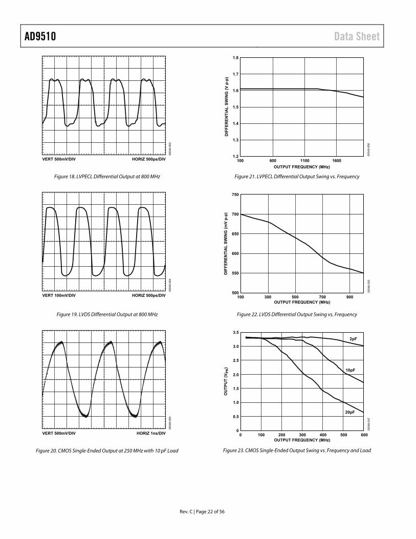
Figure 18. LVPECL Differential Output at 800 MHz
Figure 19. LVDS Differential Output at 800 MHz
Figure 20. CMOS Single-Ended Output at 250 MHz with 10 pF Load
Figure 21. LVPECL Differential Output Swing vs. Frequency
Figure 22. LVDS Differential Output Swing vs. Frequency
Figure 23. CMOS Single-Ended Output Swing vs. Frequency and Load
0504
6-05
3
VERT 500mV/DIV HORIZ 500ps/DIV
0504
6-05
4
VERT 100mV/DIV HORIZ 500ps/DIV
0504
6-05
5
VERT 500mV/DIV HORIZ 1ns/DIV
050
46
-05
6
OUTPUT FREQUENCY (MHz)
DIF
FE
RE
NT
IAL
SW
ING
(V
p-p
)
100 160011006001.2
1.3
1.4
1.5
1.6
1.7
1.8
0504
6-05
0
OUTPUT FREQUENCY (MHz)
DIF
FE
RE
NT
IAL
SW
ING
(m
V p
-p)
100 900700500300500
750
700
650
600
550
0504
6-04
7
OUTPUT FREQUENCY (MHz)
OU
TP
UT
(V
PK
)
0 6005004003002001000
3.5
3.0
2.5
2.0
1.5
1.0
0.5
2pF
10pF
20pF
Data Sheet AD9510
Rev. C | Page 23 of 56
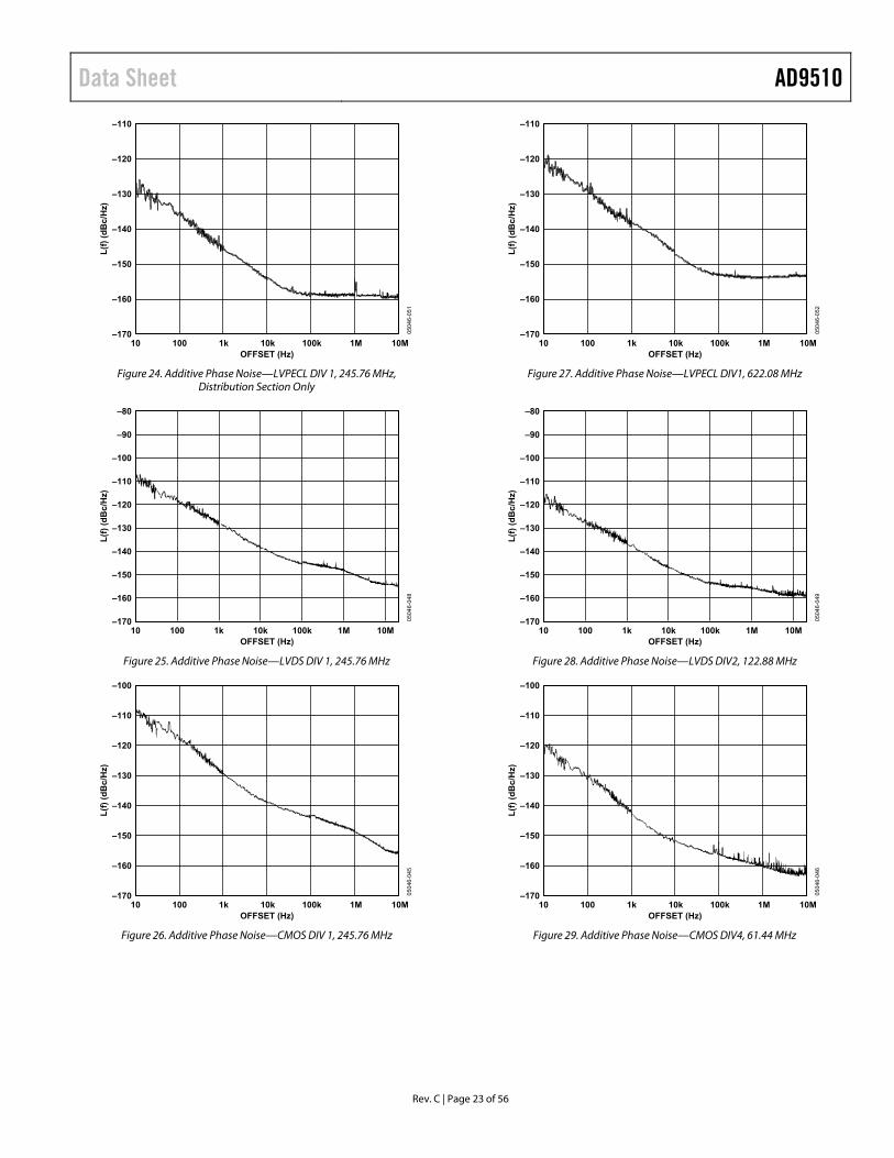
Figure 24. Additive Phase Noise—LVPECL DIV 1, 245.76 MHz,
Distribution Section Only
Figure 25. Additive Phase Noise—LVDS DIV 1, 245.76 MHz
Figure 26. Additive Phase Noise—CMOS DIV 1, 245.76 MHz
Figure 27. Additive Phase Noise—LVPECL DIV1, 622.08 MHz
Figure 28. Additive Phase Noise—LVDS DIV2, 122.88 MHz
Figure 29. Additive Phase Noise—CMOS DIV4, 61.44 MHz
0504
6-05
1
OFFSET (Hz)
L(f)
(dB
c/H
z)
10 10M1M100k10k1k100–170
–110
–130
–120
–140
–150
–160
0504
6-04
8
OFFSET (Hz)
L(f)
(dB
c/H
z)
10 10M1M100k10k1k100–170
–80
–90
–110
–100
–120
–130
–140
–150
–160
0504
6-04
5
OFFSET (Hz)
L(f)
(dB
c/H
z)
10 10M1M100k10k1k100–170
–100
–110
–120
–130
–140
–150
–160
0504
6-05
2
OFFSET (Hz)
L(f)
(dB
c/H
z)
10 10M1M100k10k1k100–170
–110
–130
–120
–140
–150
–160
0504
6-04
9
OFFSET (Hz)
L(f)
(dB
c/H
z)
10 10M1M100k10k1k100–170
–80
–90
–110
–100
–120
–130
–140
–150
–160
0504
6-04
6
OFFSET (Hz)
L(f)
(dB
c/H
z)
10 10M1M100k10k1k100–170
–100
–110
–120
–130
–140
–150
–160
AD9510 Data Sheet
Rev. C | Page 24 of 56
TERMINOLOGY Phase Jitter and Phase Noise An ideal sine wave has a continuous and even progression of phase with time from 0 to 360 degrees for each cycle. Actual signals, however, display a certain amount of variation from ideal phase progression over time. This phenomenon is called phase jitter. Although many causes can contribute to phase jitter, one major cause is random noise, which is characterized statistically as being Gaussian (normal) in distribution.
This phase jitter leads to a spreading out of the energy of the sine wave in the frequency domain, producing a continuous power spectrum. This power spectrum is usually reported as a series of values whose units are dBc/Hz at a given offset in fre-quency from the sine wave (carrier). The value is a ratio, expressed in dB, of the power contained within a 1 Hz bandwidth with respect to the power at the carrier frequency. For each measure-ment, the offset from the carrier frequency is also given.
It is meaningful to integrate the total power contained within some interval of offset frequencies (for example, 10 kHz to 10 MHz). This is called the integrated phase noise over that frequency offset interval and can be readily related to the time jitter due to the phase noise within that offset frequency interval.
Phase noise has a detrimental effect on the performance of analog-to-digital converters (ADCs), digital-to-analog converters (DACs), and signal input (RF) mixers. It lowers the achievable dynamic range of the converters and mixers, although they are affected in different ways.
Time Jitter Phase noise is a frequency domain phenomenon. In the time domain, the same effect is exhibited as time jitter. When observing a sine wave, the time of successive zero crossings is seen to vary. In a square wave, the time jitter is seen as a displacement of the edges from their ideal (regular) times of occurrence. In both cases, the variations in timing from the ideal are the time jitter. Since these variations are random in nature, the time jitter is specified in units of seconds root mean square (rms) or 1 sigma of the Gaussian distribution.
Time jitter that occurs on a sampling clock for a DAC or an ADC decreases the SNR and dynamic range of the converter. A sampling clock with the lowest possible jitter provides the highest performance from a given converter.
Additive Phase Noise Additive phase noise is the amount of phase noise attributable to the device or subsystem being measured. The phase noise of any external oscillators or clock sources is subtracted. This makes it possible to predict the degree to which the device impacts the total system phase noise when used in conjunction with the various oscillators and clock sources, each of which contribute their own phase noise to the total. In many cases, the phase noise of one element dominates the system phase noise.
Additive Time Jitter Additive time jitter is the amount of time jitter attributable to the device or subsystem being measured. The time jitter of any external oscillators or clock sources is subtracted. This makes it possible to predict the degree to which the device impacts the total system time jitter when used in conjunction with the various oscillators and clock sources, each of which contribute their own time jitter to the total. In many cases, the time jitter of the external oscillators and clock sources dominates the system time jitter.
Data Sheet AD9510
Rev. C | Page 25 of 56
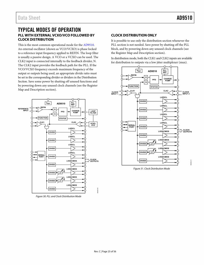
TYPICAL MODES OF OPERATION PLL WITH EXTERNAL VCXO/VCO FOLLOWED BY CLOCK DISTRIBUTION This is the most common operational mode for the AD9510. An external oscillator (shown as VCO/VCXO) is phase locked to a reference input frequency applied to REFIN. The loop filter is usually a passive design. A VCO or a VCXO can be used. The CLK2 input is connected internally to the feedback divider, N. The CLK2 input provides the feedback path for the PLL. If the VCO/VCXO frequency exceeds maximum frequency of the output or outputs being used, an appropriate divide ratio must be set in the corresponding divider or dividers in the Distribution Section. Save some power by shutting off unused functions and by powering down any unused clock channels (see the Register Map and Description section).
Figure 30. PLL and Clock Distribution Mode
CLOCK DISTRIBUTION ONLY It is possible to use only the distribution section whenever the PLL section is not needed. Save power by shutting off the PLL block, and by powering down any unused clock channels (see the Register Map and Description section).
In distribution mode, both the CLK1 and CLK2 inputs are available for distribution to outputs via a low jitter multiplexer (mux).
Figure 31. Clock Distribution Mode
0504
6-01
0
R
NPFD
STATUS
CHARGEPUMP
LVDS/CMOS
DIVIDE
LVDS/CMOS
DIVIDE
LVPECL
DIVIDE
LVPECL
DIVIDE
LVPECL
DIVIDE
LVPECL
DIVIDE
LVDS/CMOS
DIVIDE
LVDS/CMOS
DIVIDE
∆T
∆T
SERIALPORT
FUNCTION
VREF AD9510 PLLREF
CLK1 CLK2
REFERENCEINPUT
REFIN
LOOPFILTER
VCXO,VCO
CLOCKOUTPUTS
0504
6-01
1
R
NPFD
STATUS
CHARGEPUMP
LVDS/CMOS
DIVIDE
LVDS/CMOS
DIVIDE
LVPECL
DIVIDE
LVPECL
DIVIDE
LVPECL
DIVIDE
LVPECL
DIVIDE
LVDS/CMOS
DIVIDE
LVDS/CMOS
DIVIDE
∆T
∆T
SERIALPORT
FUNCTION
VREF AD9510 PLLREF
CLK1 CLK2CLOCK
INPUT 1
REFIN
CLOCKINPUT 2
CLOCKOUTPUTS
AD9510 Data Sheet
Rev. C | Page 26 of 56
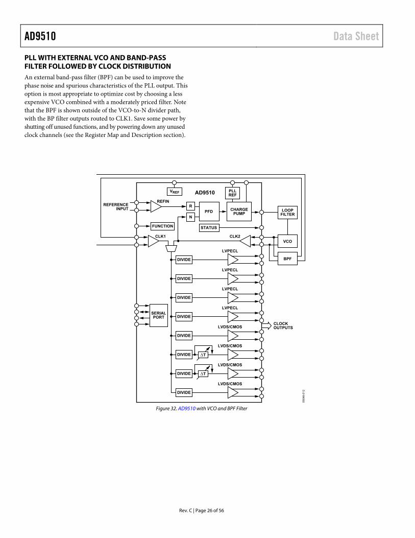
PLL WITH EXTERNAL VCO AND BAND-PASS FILTER FOLLOWED BY CLOCK DISTRIBUTION An external band-pass filter (BPF) can be used to improve the phase noise and spurious characteristics of the PLL output. This option is most appropriate to optimize cost by choosing a less expensive VCO combined with a moderately priced filter. Note that the BPF is shown outside of the VCO-to-N divider path, with the BP filter outputs routed to CLK1. Save some power by shutting off unused functions, and by powering down any unused clock channels (see the Register Map and Description section).
Figure 32. AD9510 with VCO and BPF Filter
0504
6-01
2
R
NPFD
STATUS
CHARGEPUMP
LVDS/CMOS
DIVIDE
LVDS/CMOS
DIVIDE
LVPECL
DIVIDE
LVPECL
DIVIDE
LVPECL
DIVIDE
LVPECL
DIVIDE
LVDS/CMOS
DIVIDE
LVDS/CMOS
DIVIDE
∆T
∆T
SERIALPORT
FUNCTION
VREF AD9510 PLLREF
CLK1 CLK2
REFERENCEINPUT
REFIN
LOOPFILTER
VCO
BPF
CLOCKOUTPUTS
Data Sheet AD9510
Rev. C | Page 27 of 56
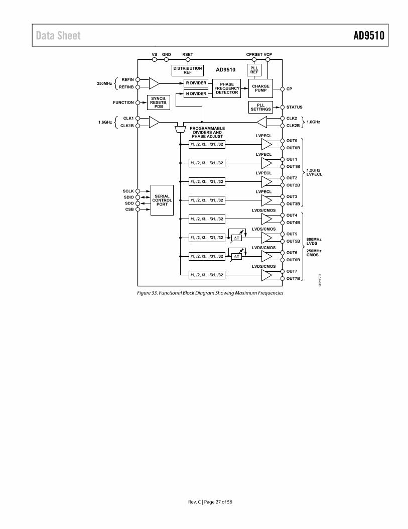
Figure 33. Functional Block Diagram Showing Maximum Frequencies
0504
6-01
3
R DIVIDER
N DIVIDER
CHARGEPUMP
PLLSETTINGS
CLK2
STATUS
CLK2BPROGRAMMABLE
DIVIDERS ANDPHASE ADJUST
OUT7
OUT7B
LVDS/CMOS
/1, /2, /3... /31, /32
OUT6
OUT6B
LVDS/CMOS
/1, /2, /3... /31, /32
OUT0
OUT0B
LVPECL
/1, /2, /3... /31, /32
OUT1
OUT1B
LVPECL
/1, /2, /3... /31, /32
OUT2
OUT2B
LVPECL
/1, /2, /3... /31, /32
OUT3
OUT3B
LVPECL
/1, /2, /3... /31, /32
OUT4
OUT4B
LVDS/CMOS
/1, /2, /3... /31, /32
OUT5
OUT5B
LVDS/CMOS
/1, /2, /3... /31, /32
CLK1
CLK1B
REFIN250MHz
REFINB
FUNCTION
SCLKSDIOSDOCSB
SERIALCONTROL
PORT
CP
CPRSET
DISTRIBUTIONREF
SYNCB,RESETB,
PDB
RSET
AD9510
GNDVS VCP
PLLREF
PHASEFREQUENCYDETECTOR
1.6GHz 1.6GHz
1.2GHzLVPECL
250MHzCMOS
800MHzLVDS
∆T
∆T
AD9510 Data Sheet
Rev. C | Page 28 of 56
FUNCTIONAL DESCRIPTION OVERALL Figure 33 shows a block diagram of the AD9510. The chip combines a programmable PLL core with a configurable clock distribution system. A complete PLL requires the addition of a suitable external VCO (or VCXO) and loop filter. This PLL can lock to a reference input signal and produce an output that is related to the input frequency by the ratio defined by the pro-grammable R and N dividers. The PLL cleans up some jitter from the external reference signal, depending on the loop band-width and the phase noise performance of the VCO (VCXO).
The output from the VCO (VCXO) can be applied to the clock distribution section of the chip, where it can be divided by any integer value from 1 to 32. The duty cycle and relative phase of the outputs can be selected. There are four LVPECL outputs, (OUT0, OUT1, OUT2, and OUT3) and four outputs that can be either LVDS or CMOS level outputs (OUT4, OUT5, OUT6, and OUT7). Two of these outputs (OUT5 and OUT6) can also make use of a variable delay block.
Alternatively, the clock distribution section can be driven directly by an external clock signal, and the PLL can be powered off. Whenever the clock distribution section is used alone, there is no clock cleanup. The jitter of the input clock signal is passed along directly to the distribution section and may dominate at the clock outputs.
PLL SECTION The AD9510 consists of a PLL section and a distribution section. If desired, the PLL section can be used separately from the distribution section.
The AD9510 has a complete PLL core on-chip, requiring only an external loop filter and VCO/VCXO. This PLL is based on the ADF4106, a PLL noted for its superb low phase noise per-formance. The operation of the AD9510 PLL is nearly identical to that of the ADF4106, offering an advantage to those with experience with the ADF series of PLLs. Differences include the addition of differential inputs at REFIN and CLK2, a different control register architecture. Also, the prescaler is changed to allow N as low as 1. The AD9510 PLL implements the digital lock detect feature somewhat differently than the ADF4106 does, offering improved functionality at higher PFD rates. See the Register Map Description section.
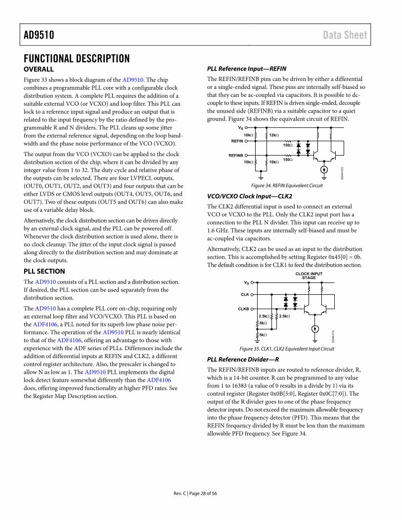
PLL Reference Input—REFIN
The REFIN/REFINB pins can be driven by either a differential or a single-ended signal. These pins are internally self-biased so that they can be ac-coupled via capacitors. It is possible to dc-couple to these inputs. If REFIN is driven single-ended, decouple the unused side (REFINB) via a suitable capacitor to a quiet ground. Figure 34 shows the equivalent circuit of REFIN.
Figure 34. REFIN Equivalent Circuit
VCO/VCXO Clock Input—CLK2
The CLK2 differential input is used to connect an external VCO or VCXO to the PLL. Only the CLK2 input port has a connection to the PLL N divider. This input can receive up to 1.6 GHz. These inputs are internally self-biased and must be ac-coupled via capacitors.
Alternatively, CLK2 can be used as an input to the distribution section. This is accomplished by setting Register 0x45[0] = 0b. The default condition is for CLK1 to feed the distribution section.
Figure 35. CLK1, CLK2 Equivalent Input Circuit
PLL Reference Divider—R
The REFIN/REFINB inputs are routed to reference divider, R, which is a 14-bit counter. R can be programmed to any value from 1 to 16383 (a value of 0 results in a divide by 1) via its control register (Register 0x0B[5:0], Register 0x0C[7:0]). The output of the R divider goes to one of the phase frequency detector inputs. Do not exceed the maximum allowable frequency into the phase frequency detector (PFD). This means that the REFIN frequency divided by R must be less than the maximum allowable PFD frequency. See Figure 34.
0504
6-03
3
VS
REFIN
REFINB150Ω
150Ω
10kΩ 12kΩ
10kΩ 10kΩ
0504
6-01
6
VS
CLOCK INPUTSTAGE
CLK
CLKB
5kΩ
5kΩ
2.5kΩ 2.5kΩ
Data Sheet AD9510
Rev. C | Page 29 of 56
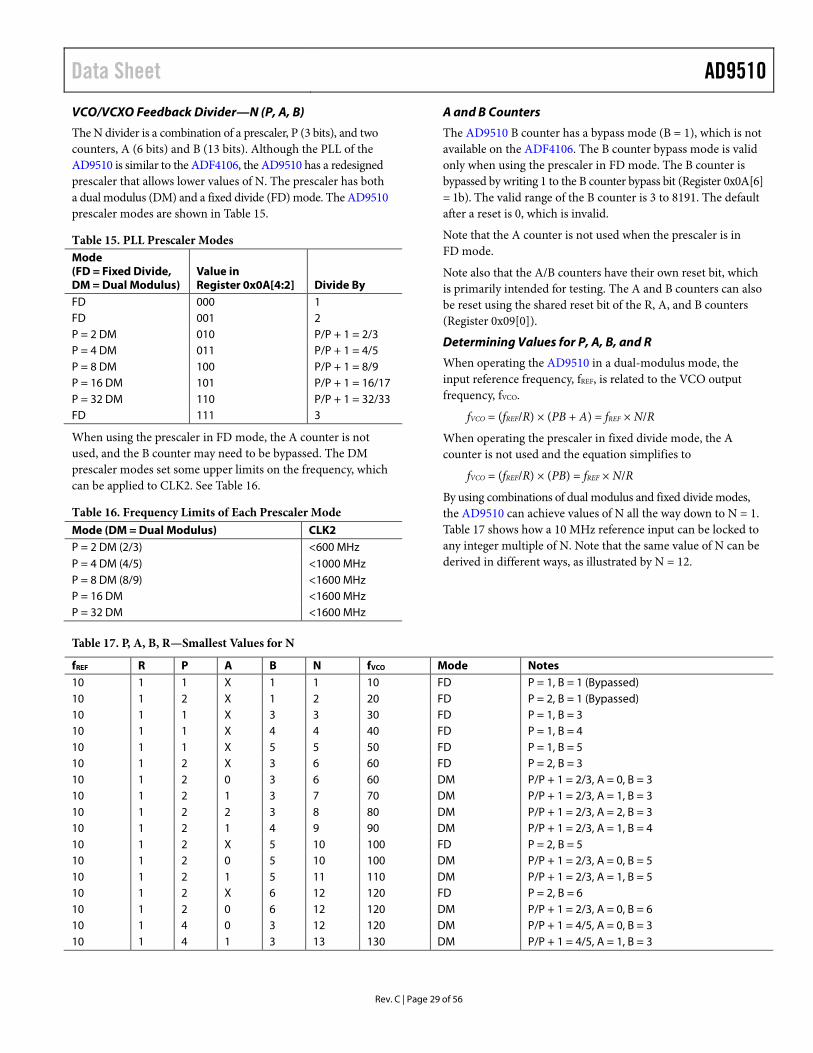
VCO/VCXO Feedback Divider—N (P, A, B)
The N divider is a combination of a prescaler, P (3 bits), and two counters, A (6 bits) and B (13 bits). Although the PLL of the AD9510 is similar to the ADF4106, the AD9510 has a redesigned prescaler that allows lower values of N. The prescaler has both a dual modulus (DM) and a fixed divide (FD) mode. The AD9510 prescaler modes are shown in Table 15.
Table 15. PLL Prescaler Modes Mode (FD = Fixed Divide, DM = Dual Modulus)
Value in Register 0x0A[4:2] Divide By
FD 000 1 FD 001 2 P = 2 DM 010 P/P + 1 = 2/3 P = 4 DM 011 P/P + 1 = 4/5 P = 8 DM 100 P/P + 1 = 8/9 P = 16 DM 101 P/P + 1 = 16/17 P = 32 DM 110 P/P + 1 = 32/33 FD 111 3
When using the prescaler in FD mode, the A counter is not used, and the B counter may need to be bypassed. The DM prescaler modes set some upper limits on the frequency, which can be applied to CLK2. See Table 16.
Table 16. Frequency Limits of Each Prescaler Mode
A and B Counters
The AD9510 B counter has a bypass mode (B = 1), which is not available on the ADF4106. The B counter bypass mode is valid only when using the prescaler in FD mode. The B counter is bypassed by writing 1 to the B counter bypass bit (Register 0x0A[6] = 1b). The valid range of the B counter is 3 to 8191. The default after a reset is 0, which is invalid.
Note that the A counter is not used when the prescaler is in FD mode.
Note also that the A/B counters have their own reset bit, which is primarily intended for testing. The A and B counters can also be reset using the shared reset bit of the R, A, and B counters (Register 0x09[0]).
Determining Values for P, A, B, and R
When operating the AD9510 in a dual-modulus mode, the input reference frequency, fREF, is related to the VCO output frequency, fVCO.
fVCO = (fREF/R) × (PB + A) = fREF × N/R
When operating the prescaler in fixed divide mode, the A counter is not used and the equation simplifies to
fVCO = (fREF/R) × (PB) = fREF × N/R
By using combinations of dual modulus and fixed divide modes, the AD9510 can achieve values of N all the way down to N = 1. Table 17 shows how a 10 MHz reference input can be locked to any integer multiple of N. Note that the same value of N can be derived in different ways, as illustrated by N = 12.
Table 17. P, A, B, R—Smallest Values for N
fREF R P A B N fVCO Mode Notes 10 1 1 X 1 1 10 FD P = 1, B = 1 (Bypassed) 10 1 2 X 1 2 20 FD P = 2, B = 1 (Bypassed) 10 1 1 X 3 3 30 FD P = 1, B = 3 10 1 1 X 4 4 40 FD P = 1, B = 4 10 1 1 X 5 5 50 FD P = 1, B = 5 10 1 2 X 3 6 60 FD P = 2, B = 3 10 1 2 0 3 6 60 DM P/P + 1 = 2/3, A = 0, B = 3 10 1 2 1 3 7 70 DM P/P + 1 = 2/3, A = 1, B = 3 10 1 2 2 3 8 80 DM P/P + 1 = 2/3, A = 2, B = 3 10 1 2 1 4 9 90 DM P/P + 1 = 2/3, A = 1, B = 4 10 1 2 X 5 10 100 FD P = 2, B = 5 10 1 2 0 5 10 100 DM P/P + 1 = 2/3, A = 0, B = 5 10 1 2 1 5 11 110 DM P/P + 1 = 2/3, A = 1, B = 5 10 1 2 X 6 12 120 FD P = 2, B = 6 10 1 2 0 6 12 120 DM P/P + 1 = 2/3, A = 0, B = 6 10 1 4 0 3 12 120 DM P/P + 1 = 4/5, A = 0, B = 3 10 1 4 1 3 13 130 DM P/P + 1 = 4/5, A = 1, B = 3
Mode (DM = Dual Modulus) CLK2 P = 2 DM (2/3) <600 MHz P = 4 DM (4/5) <1000 MHz P = 8 DM (8/9) <1600 MHz P = 16 DM <1600 MHz P = 32 DM <1600 MHz
AD9510 Data Sheet
Rev. C | Page 30 of 56
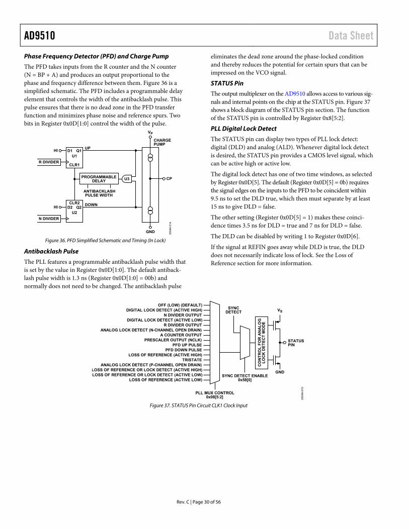
Phase Frequency Detector (PFD) and Charge Pump
The PFD takes inputs from the R counter and the N counter (N = BP + A) and produces an output proportional to the phase and frequency difference between them. Figure 36 is a simplified schematic. The PFD includes a programmable delay element that controls the width of the antibacklash pulse. This pulse ensures that there is no dead zone in the PFD transfer function and minimizes phase noise and reference spurs. Two bits in Register 0x0D[1:0] control the width of the pulse.
Figure 36. PFD Simplified Schematic and Timing (In Lock)
Antibacklash Pulse
The PLL features a programmable antibacklash pulse width that is set by the value in Register 0x0D[1:0]. The default antiback-lash pulse width is 1.3 ns (Register 0x0D[1:0] = 00b) and normally does not need to be changed. The antibacklash pulse
eliminates the dead zone around the phase-locked condition and thereby reduces the potential for certain spurs that can be impressed on the VCO signal.
STATUS Pin
The output multiplexer on the AD9510 allows access to various sig-nals and internal points on the chip at the STATUS pin. Figure 37 shows a block diagram of the STATUS pin section. The function of the STATUS pin is controlled by Register 0x8[5:2].
PLL Digital Lock Detect
The STATUS pin can display two types of PLL lock detect: digital (DLD) and analog (ALD). Whenever digital lock detect is desired, the STATUS pin provides a CMOS level signal, which can be active high or active low.
The digital lock detect has one of two time windows, as selected by Register 0x0D[5]. The default (Register 0x0D[5] = 0b) requires the signal edges on the inputs to the PFD to be coincident within 9.5 ns to set the DLD true, which then must separate by at least 15 ns to give DLD = false.
The other setting (Register 0x0D[5] = 1) makes these coinci-dence times 3.5 ns for DLD = true and 7 ns for DLD = false.
The DLD can be disabled by writing 1 to Register 0x0D[6].
If the signal at REFIN goes away while DLD is true, the DLD does not necessarily indicate loss of lock. See the Loss of Reference section for more information.
Figure 37. STATUS Pin Circuit CLK1 Clock Input
0504
6-01
4
D1 Q1U1
CLR1R DIVIDER
HI UP
D2 Q2U2
CLR2
N DIVIDER
HI DOWN
CP
CHARGEPUMP
VP
GND
U3PROGRAMMABLEDELAY
ANTIBACKLASHPULSE WIDTH
0504
6-01
5OFF (LOW) (DEFAULT)
DIGITAL LOCK DETECT (ACTIVE HIGH)N DIVIDER OUTPUT
DIGITAL LOCK DETECT (ACTIVE LOW)R DIVIDER OUTPUT
ANALOG LOCK DETECT (N-CHANNEL OPEN DRAIN)A COUNTER OUTPUT
PRESCALER OUTPUT (NCLK)PFD UP PULSE
PFD DOWN PULSELOSS OF REFERENCE (ACTIVE HIGH)
TRISTATEANALOG LOCK DETECT (P-CHANNEL OPEN DRAIN)
LOSS OF REFERENCE OR LOCK DETECT (ACTIVE HIGH)LOSS OF REFERENCE OR LOCK DETECT (ACTIVE LOW)
LOSS OF REFERENCE (ACTIVE LOW)
PLL MUX CONTROL0x08[5:2]
SYNC DETECT ENABLE0x58[0]
SYNCDETECT
CO
NTR
OL
FOR
AN
ALO
GLO
CK
DET
ECT
MO
DE
VS
GND
STATUSPIN
Data Sheet AD9510
Rev. C | Page 31 of 56
PLL Analog Lock Detect
An analog lock detect (ALD) signal can be selected. When ALD is selected, the signal at the STATUS pin is either an open-drain P-channel (Register 0x08[5:2] = 1100) or an open-drain N-channel (Register 0x08[5:2] = 0101b).
The analog lock detect signal is true (relative to the selected mode) with brief false pulses. These false pulses shorten as the inputs to the PFD are nearer to coincidence and longer as they are further from coincidence.
To extract a usable analog lock detect signal, an external resistor-capacitor (RC) network is required to provide an analog filter with the appropriate RC constant to allow for the discrimina-tion of a lock condition by an external voltage comparator. A 1 kΩ resistor in parallel with a small capacitance usually fulfills this requirement. However, some experimentation may be required to obtain the desired operation.
The analog lock detect function may introduce some spurious energy into the clock outputs. It is prudent to limit the use of the ALD when the best possible jitter/phase noise performance is required on the clock outputs.
Loss of Reference
The AD9510 PLL can warn of a loss of reference signal at REFIN. The loss of reference monitor internally sets a flag called LREF. Externally, this signal can be observed in several ways on the STATUS pin, depending on the PLL MUX control settings in Register 0x08[5:2]. The LREF alone can be observed as an active high signal by setting Register 0x08[5:2] = [1010] or as an active low signal by setting Register 0x08[5:2] = [1111].
The loss of reference circuit is clocked by the signal from the VCO, which means that there must be a VCO signal present to detect a loss of reference.
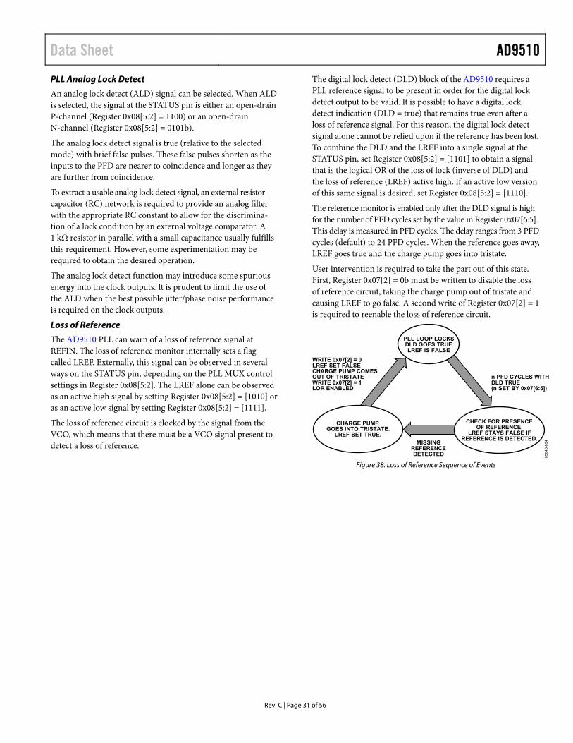
The digital lock detect (DLD) block of the AD9510 requires a PLL reference signal to be present in order for the digital lock detect output to be valid. It is possible to have a digital lock detect indication (DLD = true) that remains true even after a loss of reference signal. For this reason, the digital lock detect signal alone cannot be relied upon if the reference has been lost. To combine the DLD and the LREF into a single signal at the STATUS pin, set Register 0x08[5:2] = [1101] to obtain a signal that is the logical OR of the loss of lock (inverse of DLD) and the loss of reference (LREF) active high. If an active low version of this same signal is desired, set Register 0x08[5:2] = [1110].
The reference monitor is enabled only after the DLD signal is high for the number of PFD cycles set by the value in Register 0x07[6:5]. This delay is measured in PFD cycles. The delay ranges from 3 PFD cycles (default) to 24 PFD cycles. When the reference goes away, LREF goes true and the charge pump goes into tristate.
User intervention is required to take the part out of this state. First, Register 0x07[2] = 0b must be written to disable the loss of reference circuit, taking the charge pump out of tristate and causing LREF to go false. A second write of Register 0x07[2] = 1 is required to reenable the loss of reference circuit.
Figure 38. Loss of Reference Sequence of Events
05
04
6-0
34
PLL LOOP LOCKSDLD GOES TRUELREF IS FALSE
CHECK FOR PRESENCEOF REFERENCE.
LREF STAYS FALSE IFREFERENCE IS DETECTED.
CHARGE PUMPGOES INTO TRISTATE.
LREF SET TRUE.MISSING
REFERENCEDETECTED
n PFD CYCLES WITHDLD TRUE(n SET BY 0x07[6:5])
WRITE 0x07[2] = 0LREF SET FALSECHARGE PUMP COMESOUT OF TRISTATEWRITE 0x07[2] = 1LOR ENABLED
AD9510 Data Sheet
Rev. C | Page 32 of 56
FUNCTION PIN The FUNCTION pin (16) has three functions that are selected by the value in Register 0x58[6:5]. This pin is internally pulled down by a 30 kΩ resistor. If this pin is left unconnected, the part is in reset by default. To avoid this, connect this pin to VS with a 1 kΩ resistor.
RESETB: Register 0x58[6:5] = 00b (Default)
In its default mode, the FUNCTION pin acts as RESETB, which generates an asynchronous reset or hard reset when pulled low. The resulting reset writes the default values into the serial control port buffer registers as well as loading them into the chip control registers. When the RESETB signal goes high again, a synchro-nous sync is issued (see the SYNCB: Register 0x58[6:5] = 01b section) and the AD9510 resumes operation according to the default values of the registers.
SYNCB: Register 0x58[6:5] = 01b
Using the FUNCTION pin causes a synchronization or alignment of phase among the various clock outputs. The synchronization applies only to clock outputs that
• Are not powered down • The divider is not masked (no sync = 0b) • Are not bypassed (bypass = 0b)
SYNCB is level and rising edge sensitive. When SYNCB is low, the set of affected outputs are held in a predetermined state, defined by the start high bit of each divider. On a rising edge, the dividers begin after a predefined number of fast clock cycles (fast clock is the selected clock input, CLK1 or CLK2) as determined by the values in the phase offset bits of the divider.
The SYNCB application of the FUNCTION pin is always active, regardless of whether the pin is also assigned to perform reset or power-down. When the SYNCB function is selected, the FUNCTION pin does not act as either RESETB or PDB.
PDB: Register 0x58[6:5] = 11b
The FUNCTION pin can also be programmed to work as an asynchronous full power-down, PDB. Even in this full power-down mode, there is still some residual VS current because some on-chip references continue to operate. In PDB mode, the FUNCTION pin is active low. The chip remains in a power-down state until PDB is returned to logic high. The chip returns to the settings programmed prior to the power-down.
See the Chip Power-Down or Sleep Mode—PDB section for more details on what occurs during a PDB initiated power-down.
DISTRIBUTION SECTION As previously mentioned, the AD9510 is partitioned into two operational sections: PLL and distribution. The PLL Section is discussed previously in this data sheet. If desired, the distribution section can be used separately from the PLL section.
CLK1 AND CLK2 CLOCK INPUTS Either CLK1 or CLK2 can be selected as the input to the distri-bution section. The CLK1 input can be connected to drive the distribution section only. CLK1 is selected as the source for the distribution section by setting Register 0x45[0] = 1. This is the power-up default state.
CLK1 and CLK2 work for inputs up to 1600 MHz. A higher input slew rate improves the jitter performance. The input level must be between approximately 150 mV p-p to no more than 2 V p-p. Anything greater may result in turning on the protection diodes on the input pins, which may degrade the jitter performance.
See Figure 35 for the CLK1 and CLK2 equivalent input circuit. These inputs are fully differential and self-biased. The signal must be ac-coupled using capacitors. If a single-ended input must be used, this can be accommodated by ac-coupling to one side of the differential input only. Bypass the other side of the input to a quiet ac ground by a capacitor.
Power down the unselected clock input (CLK1 or CLK2) to eliminate any possibility of unwanted crosstalk between the selected clock input and the unselected clock input.
DIVIDERS Each of the eight clock outputs of the AD9510 has its own divider. The divider can be bypassed to obtain an output at the same frequency as the input (1×). When a divider is bypassed, it is powered down to save power.
All integer divide ratios from 1 to 32 can be selected. A divide ratio of 1 is selected by bypassing the divider.
Each divider can be configured for divide ratio, phase, and duty cycle. The phase and duty cycle values that can be selected depend on the divide ratio that is chosen.
Setting the Divide Ratio
The divide ratio is determined by the values written via the serial control port (SCP) to the registers that control each individual output, OUT0 to OUT7. These are the even numbered registers beginning at Register 0x48 and going through Register 0x56. Each of these registers is divided into bits that control the number of clock cycles that the divider output stays high (HIGH_CYCLES[3:0]) and the number of clock cycles that the divider output stays low (LOW_CYCLES[7:4]). Each value is 4 bits and has the range of 0 to 15.
The divide ratio is set by
Divide Ratio = (HIGH_CYCLES + 1) + (LOW_CYCLES + 1)
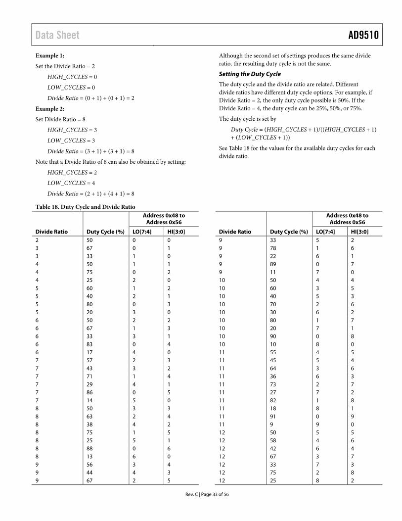
Data Sheet AD9510
Rev. C | Page 33 of 56
Example 1:
Set the Divide Ratio = 2
HIGH_CYCLES = 0
LOW_CYCLES = 0
Divide Ratio = (0 + 1) + (0 + 1) = 2
Example 2:
Set Divide Ratio = 8
HIGH_CYCLES = 3
LOW_CYCLES = 3
Divide Ratio = (3 + 1) + (3 + 1) = 8
Note that a Divide Ratio of 8 can also be obtained by setting:
HIGH_CYCLES = 2
LOW_CYCLES = 4
Divide Ratio = (2 + 1) + (4 + 1) = 8
Although the second set of settings produces the same divide ratio, the resulting duty cycle is not the same.
Setting the Duty Cycle
The duty cycle and the divide ratio are related. Different divide ratios have different duty cycle options. For example, if Divide Ratio = 2, the only duty cycle possible is 50%. If the Divide Ratio = 4, the duty cycle can be 25%, 50%, or 75%.
The duty cycle is set by
Duty Cycle = (HIGH_CYCLES + 1)/((HIGH_CYCLES + 1) + (LOW_CYCLES + 1))
See Table 18 for the values for the available duty cycles for each divide ratio.
Table 18. Duty Cycle and Divide Ratio
Divide Ratio Duty Cycle (%)
Address 0x48 to Address 0x56
LO[7:4] HI[3:0] 2 50 0 0 3 67 0 1 3 33 1 0 4 50 1 1 4 75 0 2 4 25 2 0 5 60 1 2 5 40 2 1 5 80 0 3 5 20 3 0 6 50 2 2 6 67 1 3 6 33 3 1 6 83 0 4 6 17 4 0 7 57 2 3 7 43 3 2 7 71 1 4 7 29 4 1 7 86 0 5 7 14 5 0 8 50 3 3 8 63 2 4 8 38 4 2 8 75 1 5 8 25 5 1 8 88 0 6 8 13 6 0 9 56 3 4 9 44 4 3 9 67 2 5
Divide Ratio Duty Cycle (%)
Address 0x48 to Address 0x56
LO[7:4] HI[3:0] 9 33 5 2 9 78 1 6 9 22 6 1 9 89 0 7 9 11 7 0 10 50 4 4 10 60 3 5 10 40 5 3 10 70 2 6 10 30 6 2 10 80 1 7 10 20 7 1 10 90 0 8 10 10 8 0 11 55 4 5 11 45 5 4 11 64 3 6 11 36 6 3 11 73 2 7 11 27 7 2 11 82 1 8 11 18 8 1 11 91 0 9 11 9 9 0 12 50 5 5 12 58 4 6 12 42 6 4 12 67 3 7 12 33 7 3 12 75 2 8 12 25 8 2

AD9510 Data Sheet
Rev. C | Page 34 of 56
Divide Ratio Duty Cycle (%)
Address 0x48 to Address 0x56
LO[7:4] HI[3:0] 12 83 1 9 12 17 9 1 12 92 0 A 12 8 A 0 13 54 5 6 13 46 6 5 13 62 4 7 13 38 7 4 13 69 3 8 13 31 8 3 13 77 2 9 13 23 9 2 13 85 1 A 13 15 A 1 13 92 0 B 13 8 B 0 14 50 6 6 14 57 5 7 14 43 7 5 14 64 4 8 14 36 8 4 14 71 3 9 14 29 9 3 14 79 2 A 14 21 A 2 14 86 1 B 14 14 B 1 14 93 0 C 14 7 C 0 15 53 6 7 15 47 7 6 15 60 5 8 15 40 8 5 15 67 4 9 15 33 9 4 15 73 3 A 15 27 A 3 15 80 2 B 15 20 B 2 15 87 1 C 15 13 C 1 15 93 0 D 15 7 D 0 16 50 7 7 16 56 6 8 16 44 8 6 16 63 5 9 16 38 9 5 16 69 4 A 16 31 A 4
Divide Ratio Duty Cycle (%)
Address 0x48 to Address 0x56
LO[7:4] HI[3:0] 16 75 3 B 16 25 B 3 16 81 2 C 16 19 C 2 16 88 1 D 16 13 D 1 16 94 0 E 16 6 E 0 17 53 7 8 17 47 8 7 17 59 6 9 17 41 9 6 17 65 5 A 17 35 A 5 17 71 4 B 17 29 B 4 17 76 3 C 17 24 C 3 17 82 2 D 17 18 D 2 17 88 1 E 17 12 E 1 17 94 0 F 17 6 F 0 18 50 8 8 18 56 7 9 18 44 9 7 18 61 6 A 18 39 A 6 18 67 5 B 18 33 B 5 18 72 4 C 18 28 C 4 18 78 3 D 18 22 D 3 18 83 2 E 18 17 E 2 18 89 1 F 18 11 F 1 19 53 8 9 19 47 9 8 19 58 7 A 19 42 A 7 19 63 6 B 19 37 B 6 19 68 5 C 19 32 C 5 19 74 4 D 19 26 D 4 19 79 3 E
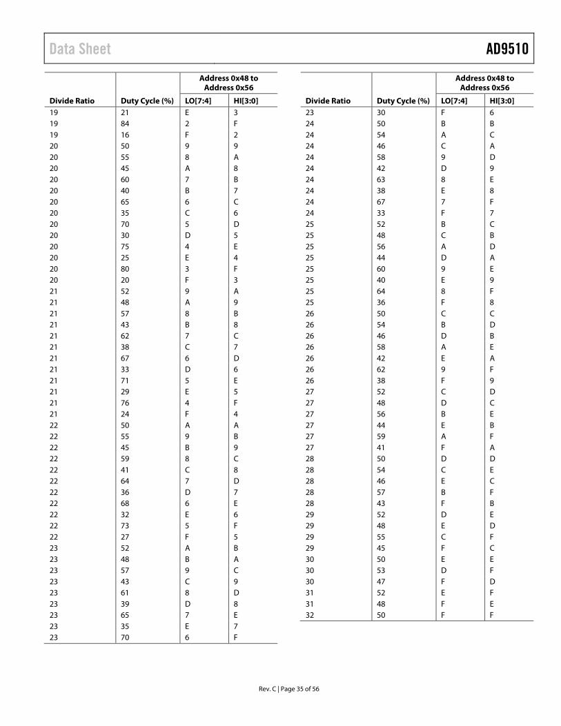
Data Sheet AD9510
Rev. C | Page 35 of 56
Divide Ratio Duty Cycle (%)
Address 0x48 to Address 0x56
LO[7:4] HI[3:0] 19 21 E 3 19 84 2 F 19 16 F 2 20 50 9 9 20 55 8 A 20 45 A 8 20 60 7 B 20 40 B 7 20 65 6 C 20 35 C 6 20 70 5 D 20 30 D 5 20 75 4 E 20 25 E 4 20 80 3 F 20 20 F 3 21 52 9 A 21 48 A 9 21 57 8 B 21 43 B 8 21 62 7 C 21 38 C 7 21 67 6 D 21 33 D 6 21 71 5 E 21 29 E 5 21 76 4 F 21 24 F 4 22 50 A A 22 55 9 B 22 45 B 9 22 59 8 C 22 41 C 8 22 64 7 D 22 36 D 7 22 68 6 E 22 32 E 6 22 73 5 F 22 27 F 5 23 52 A B 23 48 B A 23 57 9 C 23 43 C 9 23 61 8 D 23 39 D 8 23 65 7 E 23 35 E 7 23 70 6 F
Divide Ratio Duty Cycle (%)
Address 0x48 to Address 0x56
LO[7:4] HI[3:0] 23 30 F 6 24 50 B B 24 54 A C 24 46 C A 24 58 9 D 24 42 D 9 24 63 8 E 24 38 E 8 24 67 7 F 24 33 F 7 25 52 B C 25 48 C B 25 56 A D 25 44 D A 25 60 9 E 25 40 E 9 25 64 8 F 25 36 F 8 26 50 C C 26 54 B D 26 46 D B 26 58 A E 26 42 E A 26 62 9 F 26 38 F 9 27 52 C D 27 48 D C 27 56 B E 27 44 E B 27 59 A F 27 41 F A 28 50 D D 28 54 C E 28 46 E C 28 57 B F 28 43 F B 29 52 D E 29 48 E D 29 55 C F 29 45 F C 30 50 E E 30 53 D F 30 47 F D 31 52 E F 31 48 F E 32 50 F F

AD9510 Data Sheet
Rev. C | Page 36 of 56
Divider Phase Offset
The phase of each output can be selected, depending on the divide ratio chosen. This is selected by writing the appropriate values to the registers which set the phase and start high/low bit for each output. These are the odd numbered registers from Register 0x49 to Register 0x57. Each divider has a 4-bit phase offset [3:0] and a start high or low bit [4].
Following a sync pulse, the phase offset word determines how many fast clock (CLK1 or CLK2) cycles to wait before initiating a clock output edge. The Start H/L bit determines if the divider output starts low or high. By giving each divider a different phase offset, output-to-output delays can be set in increments of the fast clock period, tCLK.
Figure 39 shows four dividers, each set for DIV = 4, 50% duty cycle. By incrementing the phase offset from 0 to 3, each output is offset from the initial edge by a multiple of tCLK.
Figure 39. Phase Offset—All Dividers Set for DIV = 4, Phase Set from 0 to 3
For example:
CLK1 = 491.52 MHz
tCLK1 = 1/491.52 = 2.0345 ns
For DIV = 4
Phase Offset 0 = 0 ns
Phase Offset 1 = 2.0345 ns
Phase Offset 2 = 4.069 ns
Phase Offset 3 = 6.104 ns
The four outputs can also be described as:
OUT1 = 0°
OUT2 = 90°
OUT3 = 180°
OUT4 = 270°
Setting the phase offset to Phase = 4 results in the same relative phase as the first channel, Phase = 0° or 360°.
In general, by combining the 4-bit phase offset and the Start H/L bit, there are 32 possible phase offset states (see Table 19).
Table 19. Phase Offset—Start H/L Bit Phase Offset (Fast Clock Rising Edges)
Address 0x49 to Address 0x57
Phase Offset[3:0] Start H/L[4] 0 0 0 1 1 0 2 2 0 3 3 0 4 4 0 5 5 0 6 6 0 7 7 0 8 8 0 9 9 0 10 10 0 11 11 0 12 12 0 13 13 0 14 14 0 15 15 0 16 0 1 17 1 1 18 2 1 19 3 1 20 4 1 21 5 1 22 6 1 23 7 1 24 8 1 25 9 1 26 10 1 27 11 1 28 12 1 29 13 1 30 14 1 31 15 1
The resolution of the phase offset is set by the fast clock period (tCLK) at CLK1 or CLK2. As a result, every divide ratio does not have 32 unique phase offsets available. For any divide ratio, the number of unique phase offsets is numerically equal to the divide ratio (see Table 19):
DIV = 4
Unique Phase Offsets Are Phase = 0, 1, 2, 3
DIV= 7
Unique Phase Offsets Are Phase = 0, 1, 2, 3, 4, 5, 6
DIV = 18
Unique Phase Offsets Are Phase = 0, 1, 2, 3, 4, 5, 6, 7, 8, 9, 10, 11, 12, 13, 14, 15, 16, 17
0504
6-03
5
CLOCK INPUTCLK
DIVIDER OUTPUTSDIV = 4, DUTY = 50%
START = 0,PHASE = 0
START = 0,PHASE = 1
START = 0,PHASE = 2
START = 0,PHASE = 3
0 1 2 3 4 5 6 7 8 9 10 11 12 13 14 15
tCLK
tCLK
2 × tCLK
3 × tCLK
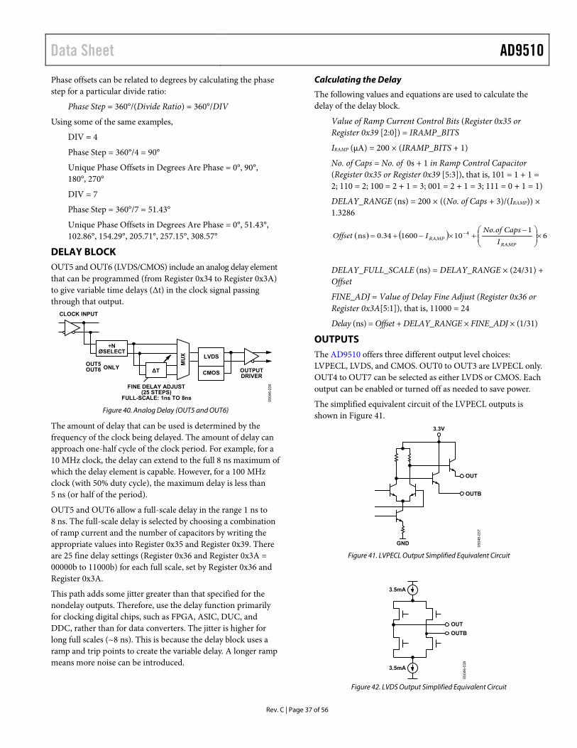
Data Sheet AD9510
Rev. C | Page 37 of 56
Phase offsets can be related to degrees by calculating the phase step for a particular divide ratio:
Phase Step = 360°/(Divide Ratio) = 360°/DIV
Using some of the same examples,
DIV = 4
Phase Step = 360°/4 = 90°
Unique Phase Offsets in Degrees Are Phase = 0°, 90°, 180°, 270°
DIV = 7
Phase Step = 360°/7 = 51.43°
Unique Phase Offsets in Degrees Are Phase = 0°, 51.43°, 102.86°, 154.29°, 205.71°, 257.15°, 308.57°
DELAY BLOCK OUT5 and OUT6 (LVDS/CMOS) include an analog delay element that can be programmed (from Register 0x34 to Register 0x3A) to give variable time delays (Δt) in the clock signal passing through that output.
Figure 40. Analog Delay (OUT5 and OUT6)
The amount of delay that can be used is determined by the frequency of the clock being delayed. The amount of delay can approach one-half cycle of the clock period. For example, for a 10 MHz clock, the delay can extend to the full 8 ns maximum of which the delay element is capable. However, for a 100 MHz clock (with 50% duty cycle), the maximum delay is less than 5 ns (or half of the period).
OUT5 and OUT6 allow a full-scale delay in the range 1 ns to 8 ns. The full-scale delay is selected by choosing a combination of ramp current and the number of capacitors by writing the appropriate values into Register 0x35 and Register 0x39. There are 25 fine delay settings (Register 0x36 and Register 0x3A = 00000b to 11000b) for each full scale, set by Register 0x36 and Register 0x3A.
This path adds some jitter greater than that specified for the nondelay outputs. Therefore, use the delay function primarily for clocking digital chips, such as FPGA, ASIC, DUC, and DDC, rather than for data converters. The jitter is higher for long full scales (~8 ns). This is because the delay block uses a ramp and trip points to create the variable delay. A longer ramp means more noise can be introduced.
Calculating the Delay
The following values and equations are used to calculate the delay of the delay block.
Value of Ramp Current Control Bits (Register 0x35 or Register 0x39 [2:0]) = IRAMP_BITS
IRAMP (µA) = 200 × (IRAMP_BITS + 1)
No. of Caps = No. of 0s + 1 in Ramp Control Capacitor (Register 0x35 or Register 0x39 [5:3]), that is, 101 = 1 + 1 = 2; 110 = 2; 100 = 2 + 1 = 3; 001 = 2 + 1 = 3; 111 = 0 + 1 = 1)
DELAY_RANGE (ns) = 200 × ((No. of Caps + 3)/(IRAMP)) × 1.3286
( ) ( ) 61
1016000.34ns 4 ×
−+×−+= −
RAMPRAMP I
CapsofNo.IOffset
DELAY_FULL_SCALE (ns) = DELAY_RANGE × (24/31) + Offset
FINE_ADJ = Value of Delay Fine Adjust (Register 0x36 or Register 0x3A[5:1]), that is, 11000 = 24
Delay (ns) = Offset + DELAY_RANGE × FINE_ADJ × (1/31)
OUTPUTS The AD9510 offers three different output level choices: LVPECL, LVDS, and CMOS. OUT0 to OUT3 are LVPECL only. OUT4 to OUT7 can be selected as either LVDS or CMOS. Each output can be enabled or turned off as needed to save power.
The simplified equivalent circuit of the LVPECL outputs is shown in Figure 41.
Figure 41. LVPECL Output Simplified Equivalent Circuit
Figure 42. LVDS Output Simplified Equivalent Circuit
0504
6-03
6
ΔT
FINE DELAY ADJUST(25 STEPS)
FULL-SCALE: 1ns TO 8ns
OUT5OUT6 ONLY
CLOCK INPUT
÷NØSELECT
MU
X LVDS
CMOS OUTPUTDRIVER
0504
6-03
7
3.3V
OUT
OUTB
GND
0504
6-03
8
3.5mA
3.5mA
OUTOUTB
AD9510 Data Sheet
Rev. C | Page 38 of 56
POWER-DOWN MODES Chip Power-Down or Sleep Mode—PDB
The PDB chip power-down turns off most of the functions and currents in the AD9510. When the PDB mode is enabled, a chip power-down is activated by taking the FUNCTION pin to a logic low level. The chip remains in this power-down state until PDB is brought back to logic high. When woken up, the AD9510 returns to the settings programmed into its registers prior to the power-down, unless the registers are changed by new programming while the PDB mode is active.
The PDB power-down mode shuts down the currents on the chip, except the bias current necessary to maintain the LVPECL outputs in a safe shutdown mode. This is needed to protect the LVPECL output circuitry from damage that can be caused by certain termination and load configurations when tristated. Because this is not a complete power-down, it is also called sleep mode.
When the AD9510 is in a PDB power-down or sleep mode, the chip is in the following state:
• The PLL is off (asynchronous power-down). • All clocks and sync circuits are off. • All dividers are off. • All LVDS/CMOS outputs are off. • All LVPECL outputs are in safe off mode. • The serial control port is active, and the chip responds to
commands.
If the AD9510 clock outputs must be synchronized to each other, a SYNC (see the Single-Chip Synchronization section) is required upon exiting power-down mode.
PLL Power-Down
The PLL section of the AD9510 can be selectively powered down. There are three PLL power-down modes, set by the values in Register 0x0A[1:0], as shown in Table 20.
Table 20. Register 0x0A: PLL Power-Down [1] [0] Mode 0 0 Normal Operation 0 1 Asynchronous Power-Down 1 0 Normal Operation 1 1 Synchronous Power-Down
In asynchronous power-down mode, the device powers down as soon as the registers are updated.
In synchronous power-down mode, the PLL power-down is gated by the charge pump to prevent unwanted frequency jumps. The device goes into power-down on the occurrence of the next charge pump event after the registers are updated.
Distribution Power-Down
The distribution section can be powered down by writing to Register 0x58[3] = 1. This turns off the bias to the distribution section. If the LVPECL power-down mode is normal operation
[00], it is possible for a low impedance load on that LVPECL output to draw significant current during this power-down. If the LVPECL power-down mode is set to [11], the LVPECL output is not protected from reverse bias and can be damaged under certain termination conditions.
When combined with the PLL power-down, this mode results in the lowest possible power-down current for the AD9510.
Individual Clock Output Power-Down
Any of the eight clock distribution outputs can be powered down individually by writing to the appropriate registers via the SCP. The register map details the individual power-down settings for each output. The LVDS/CMOS outputs can be powered down, regardless of their output load configuration.
The LVPECL outputs have multiple power-down modes (see Register Address 3C, Register Address 3D, Register Address 3E, and Register Address 3F in Table 25). These give some flexibility in dealing with various output termination conditions. When the mode is set to [10], the LVPECL output is protected from reverse bias to 2 VBE + 1 V. If the mode is set to [11], the LVPECL output is not protected from reverse bias and can be damaged under certain termination conditions. This setting also affects the operation when the distribution block is powered down with Register 0x58[3] = 1b (see the Distribution Power-Down section).
Individual Circuit Block Power-Down
Many of the AD9510 circuit blocks (CLK1, CLK2, REFIN, and so on) can be powered down individually. This gives flexibility in configuring the part for power savings whenever certain chip functions are not needed.
RESET MODES The AD9510 has several ways to force the chip into a reset condition.
Power-On Reset—Start-Up Conditions when VS is Applied
A power-on reset (POR) is issued when the VS power supply is turned on. This initializes the chip to the power-on conditions that are determined by the default register settings. These are indicated in the default value column of Table 24.
Asynchronous Reset via the FUNCTION Pin
As mentioned in the FUNCTION Pin section, a hard reset, RESETB: Register 0x58[6:5] = 00b (Default), restores the chip to the default settings.
Soft Reset via the Serial Port
The serial control port allows a soft reset by writing to Register 0x00[5] = 1b. When this bit is set, the chip executes a soft reset. This restores the default values to the internal registers, except for Register 0x00 itself.
This bit is not self-clearing. The bit must be written to Register 0x00[5] = 0b in order for the operation of the part to continue.

Data Sheet AD9510
Rev. C | Page 39 of 56
SINGLE-CHIP SYNCHRONIZATION SYNCB—Hardware SYNC
The AD9510 clocks can be synchronized to each other at any time. The outputs of the clocks are forced into a known state with respect to each other and then allowed to continue clocking from that state in synchronicity. Before a synchronization is done, the FUNCTION Pin must be set to act as the SYNCB: Register 0x58[6:5] = 01b input (Register 0x58[6:5] = 01b). Synchronization is done by forcing the FUNCTION pin low, creating a SYNCB signal and then releasing it.
See the SYNCB: Register 0x58[6:5] = 01b section for a more detailed description of what happens when the SYNCB: Register 0x58[6:5] = 01b signal is issued.
Soft SYNC—Register 0x58[2]
A soft SYNC can be issued by means of a bit in Registers 0x58[2]. This soft SYNC works the same as the SYNCB, except that the polarity is reversed. A 1 written to this bit forces the clock outputs into a known state with respect to each other. When a 0 is subsequently written to this bit, the clock outputs continue clocking from that state in synchronicity.
MULTICHIP SYNCHRONIZATION The AD9510 provides a means of synchronizing two or more AD9510s. This is not an active synchronization; it requires user monitoring and action. The arrangement of two AD9510s to be synchronized is shown in Figure 43.
Synchronization of two or more AD9510s requires a fast clock and a slow clock. The fast clock can be up to 1 GHz and can be the clock driving the master AD9510 CLK1 input or one of the outputs of the master. The fast clock acts as the input to the distribution section of the slave AD9510 and is connected to its CLK1 input. The PLL can be used on the master, but the slave PLL is not used.
The slow clock is the clock that is synchronized across the two chips. This clock must be no faster than one-fourth of the fast clock, and no greater than 250 MHz. The slow clock is taken from one of the outputs of the master AD9510 and acts as the REFIN (or CLK2) input to the slave AD9510. One of the outputs of the slave must provide this same frequency back to the CLK2 (or REFIN) input of the slave.
Multichip synchronization is enabled by writing Register 0x58[0] = 1 on the slave AD9510. When this bit is set, the STATUS pin becomes the output for the SYNC signal. A low signal indicates an in-sync condition, and a high indicates an out-of-sync condition.
Register 0x58[1] selects the number of fast clock cycles that are the maximum separation of the slow clock edges that are con-sidered synchronized. When Register 0x58[1] = 0 (default), the slow clock edges must be coincident within 1 to 1.5 high speed clock cycles. If the coincidence of the slow clock edges is closer than this amount, the SYNC flag stays low. If the coincidence of the slow clock edges is greater than this amount, the SYNC flag is set high. When Register 0x58[1] = 1b, the amount of coincidence required is 0.5 fast clock cycles to 1 fast clock cycles.
Whenever the SYNC flag is set high, indicating an out-of-sync condition, a SYNCB signal applied simultaneously at the FUNCTION pins of both AD9510s brings the slow clocks into synchronization.
Figure 43. Multichip Synchronization
0504
6-03
9
AD9510MASTER
FAST CLOCK<1GHz
SLOW CLOCK<250MHz
AD9510SLAVE
FAST CLOCK<1GHz
SLOWCLOCK
<250MHz
SYNCDETECT
CLK2 REFIN
OUTY
OUTM
OUTN
FSYNC
FSYNC
STATUS(SYNC)
FUNCTION(SYNCB)
FUNCTION(SYNCB)
SYNCB
CLK1

AD9510 Data Sheet
Rev. C | Page 40 of 56
SERIAL CONTROL PORT The AD9510 serial control port is a flexible, synchronous, serial communications port that allows an easy interface with many industry-standard microcontrollers and microprocessors. The AD9510 serial control port is compatible with most synchronous transfer formats, including both the Motorola SPI® and Intel® SSR® protocols. The serial control port allows read/write access to all registers that configure the AD9510. Single or multiple byte transfers are supported, as well as MSB first or LSB first transfer formats. The AD9510 serial control port can be configured for a single bidirectional input/output pin (SDIO only) or for two unidirectional input/output pins (SDIO/SDO).
SERIAL CONTROL PORT PIN DESCRIPTIONS SCLK (serial clock) is the serial shift clock. This pin is an input. SCLK is used to synchronize serial control port reads and writes. Write data bits are registered on the rising edge of this clock, and read data bits are registered on the falling edge. This pin is internally pulled down by a 30 kΩ resistor to ground.
SDIO (serial data input/output) is a dual-purpose pin and acts as either an input only or as both an input/output. The AD9510 defaults to two unidirectional pins for input/output, with SDIO used as an input, and SDO as an output. Alternatively, SDIO can be used as a bidirectional input/output pin by writing to the SDO enable register at Register 0x00[7] = 1b.
SDO (serial data out) is used only in the unidirectional input/ output mode (Register 0x00[7] = 0, default) as a separate output pin for reading back data. The AD9510 defaults to this input/ output mode. Bidirectional input/output mode (using SDIO as both input and output) can be enabled by writing to the SDO enable register at Register 0x00[7] = 1.
CSB (chip select bar) is an active low control that gates the read and write cycles. When CSB is high, SDO and SDIO are in a high impedance state. This pin is internally pulled down by a 30 kΩ resistor to ground. Do not leave it unconnected or tied low. See the General Operation of Serial Control Port section on the use of the CSB in a communication cycle.
Figure 44. Serial Control Port
GENERAL OPERATION OF SERIAL CONTROL PORT Framing a Communication Cycle with CSB
Each communications cycle (a write or a read operation) is gated by the CSB line. CSB must be brought low to initiate a communication cycle. CSB must be brought high at the comple-tion of a communication cycle (see Figure 52). If CSB is not brought high at the end of each write or read cycle (on a byte boundary), the last byte is not loaded into the register buffer.
CSB stall high is supported in modes where three or fewer bytes of data (plus instruction data) are transferred (W1:W0 must be
set to 00, 01, or 10, see Table 21). In these modes, CSB can temporarily return high on any byte boundary, allowing time for the system controller to process the next byte. CSB can go high on byte boundaries only and can go high during either part (instruction or data) of the transfer. During this period, the serial control port state machine enters a wait state until all data is sent. If the system controller decides to abort the transfer before all of the data is sent, the state machine must be reset by either completing the remaining transfer or by returning the CSB low for at least one complete SCLK cycle (but less than eight SCLK cycles). Raising the CSB on a nonbyte boundary terminates the serial transfer and flushes the buffer.
In the streaming mode (W1:W0 = 11b), any number of data bytes can be transferred in a continuous stream. The register address is automatically incremented or decremented (see the MSB/LSB First Transfers section). CSB must be raised at the end of the last byte to be transferred, thereby ending the stream mode.
Communication Cycle—Instruction Plus Data
There are two parts to a communication cycle with the AD9510. The first writes a 16-bit instruction word into the AD9510, coincident with the first 16 SCLK rising edges. The instruction word provides the AD9510 serial control port with information regarding the data transfer, which is the second part of the communication cycle. The instruction word defines whether the upcoming data transfer is a read or a write, the number of bytes in the data transfer, and the starting register address for the first byte of the data transfer.
Write
If the instruction word is for a write operation (I15 = 0b), the second part is the transfer of data into the serial control port buffer of the AD9510. The length of the transfer (1, 2, 3 bytes, or streaming mode) is indicated by 2 bits (W1:W0) in the instruction byte. CSB can be raised after each sequence of 8 bits to stall the bus (except after the last byte, where it ends the cycle). When the bus is stalled, the serial transfer resumes when CSB is lowered. Stalling on nonbyte boundaries resets the serial control port.
Since data is written into a serial control port buffer area, not directly into the actual control registers of the AD9510, an addi-tional operation is needed to transfer the serial control port buffer contents to the actual control registers of the AD9510, thereby causing them to take effect. This update command consists of writing to Register 0x5A[0] = 1b. This update bit is self-clearing (it is not required to write 0 to it to clear it). Since any number of bytes of data can be changed before issuing an update command, the update simultaneously enables all register changes since any previous update.
Phase offsets or divider synchronization do not become effective until a SYNC is issued (see the Single-Chip Synchronization section).
0504
6-01
7
SCLK (PIN 18)SDIO (PIN 19)SDO (PIN 20)CSB (PIN 21)
AD9510SERIAL
CONTROLPORT
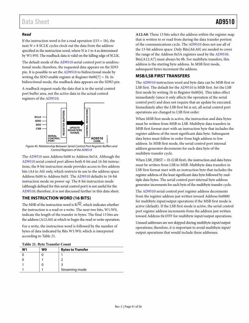
Data Sheet AD9510
Rev. C | Page 41 of 56
Read
If the instruction word is for a read operation (I15 = 1b), the next N × 8 SCLK cycles clock out the data from the address specified in the instruction word, where N is 1 to 4 as determined by W1:W0. The readback data is valid on the falling edge of SCLK.
The default mode of the AD9510 serial control port is unidirec-tional mode; therefore, the requested data appears on the SDO pin. It is possible to set the AD9510 to bidirectional mode by writing the SDO enable register at Register 0x00[7] = 1b. In bidirectional mode, the readback data appears on the SDIO pin.
A readback request reads the data that is in the serial control port buffer area, not the active data in the actual control registers of the AD9510.
Figure 45. Relationship Between Serial Control Port Register Buffers and
Control Registers of the AD9510
The AD9510 uses Address 0x00 to Address 0x5A. Although the AD9510 serial control port allows both 8-bit and 16-bit instruc-tions, the 8-bit instruction mode provides access to five address bits (A4 to A0) only, which restricts its use to the address space Address 0x00 to Address 0x01. The AD9510 defaults to 16-bit instruction mode on power-up. The 8-bit instruction mode (although defined for this serial control port) is not useful for the AD9510; therefore, it is not discussed further in this data sheet.
THE INSTRUCTION WORD (16 BITS)
The MSB of the instruction word is R/W, which indicates whether the instruction is a read or a write. The next two bits, W1:W0, indicate the length of the transfer in bytes. The final 13 bits are the address (A12:A0) at which to begin the read or write operation.
For a write, the instruction word is followed by the number of bytes of data indicated by Bits W1:W0, which is interpreted according to Table 21.
Table 21. Byte Transfer Count W1 W0 Bytes to Transfer 0 0 1 0 1 2 1 0 3 1 1 Streaming mode
A12:A0: These 13 bits select the address within the register map that is written to or read from during the data transfer portion of the communications cycle. The AD9510 does not use all of the 13-bit address space. Only Bits[A6:A0] are needed to cover the range of the Address 0x5A registers used by the AD9510. Bits[A12:A7] must always be 0b. For multibyte transfers, this address is the starting byte address. In MSB first mode, subsequent bytes increment the address.
MSB/LSB FIRST TRANSFERS The AD9510 instruction word and byte data can be MSB first or LSB first. The default for the AD9510 is MSB first. Set the LSB first mode by writing 1b to Register 0x00[6]. This takes effect immediately (since it only affects the operation of the serial control port) and does not require that an update be executed. Immediately after the LSB first bit is set, all serial control port operations are changed to LSB first order.
When MSB first mode is active, the instruction and data bytes must be written from MSB to LSB. Multibyte data transfers in MSB first format start with an instruction byte that includes the register address of the most significant data byte. Subsequent data bytes must follow in order from high address to low address. In MSB first mode, the serial control port internal address generator decrements for each data byte of the multibyte transfer cycle.
When LSB_FIRST = 1b (LSB first), the instruction and data bytes must be written from LSB to MSB. Multibyte data transfers in LSB first format start with an instruction byte that includes the register address of the least significant data byte followed by mul-tiple data bytes. The serial control port internal byte address generator increments for each byte of the multibyte transfer cycle.
The AD9510 serial control port register address decrements from the register address just written toward Address 0x0000 for multibyte input/output operations if the MSB first mode is active (default). If the LSB first mode is active, the serial control port register address increments from the address just written toward Address 0x1FFF for multibyte input/output operations.
Unused addresses are not skipped during multibyte input/output operations; therefore, it is important to avoid multibyte input/ output operations that would include these addresses.
05
04
6-0
18
SCLK
SDIO
SDO
CSB UPDATEREGISTERS
0x5A[0]SERIALCONTROLPORT
RE
GIS
TE
R B
UF
FE
RS
AD9510CORE
CO
NT
RO
L R
EG
IST
ER
S
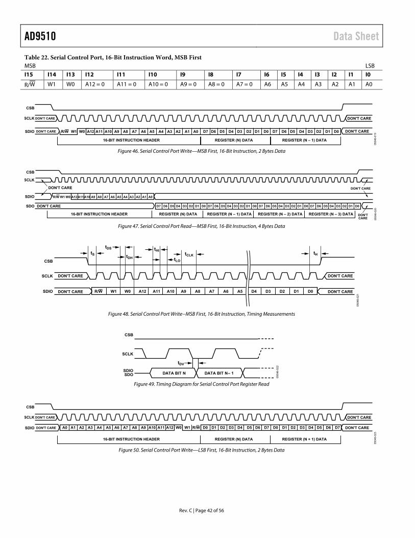
AD9510 Data Sheet
Rev. C | Page 42 of 56
Table 22. Serial Control Port, 16-Bit Instruction Word, MSB First MSB LSB
I15 I14 I13 I12 I11 I10 I9 I8 I7 I6 I5 I4 I3 I2 I1 I0
R/W W1 W0 A12 = 0 A11 = 0 A10 = 0 A9 = 0 A8 = 0 A7 = 0 A6 A5 A4 A3 A2 A1 A0
Figure 46. Serial Control Port Write—MSB First, 16-Bit Instruction, 2 Bytes Data
Figure 47. Serial Control Port Read—MSB First, 16-Bit Instruction, 4 Bytes Data
Figure 48. Serial Control Port Write−MSB First, 16-Bit Instruction, Timing Measurements
Figure 49. Timing Diagram for Serial Control Port Register Read
Figure 50. Serial Control Port Write—LSB First, 16-Bit Instruction, 2 Bytes Data
0504
6-01
9
CSB
SCLK DON'T CARE
SDIO A12W0W1R/W A11 A10 A9 A8 A7 A6 A5 A4 A3 A2 A1 A0 D7 D6 D5 D4 D3 D2 D1 D0 D7 D6 D5 D4 D3 D2 D1 D0 DON'T CAREDON'T CARE
DON'T CARE
16-BIT INSTRUCTION HEADER REGISTER (N) DATA REGISTER (N – 1) DATA
0504
6-02
0
CSB
SCLK
SDIO
SDO
REGISTER (N) DATA16-BIT INSTRUCTION HEADER REGISTER (N – 1) DATA REGISTER (N – 2) DATA REGISTER (N – 3) DATA
A12W0W1R/W A11A10 A9 A8 A7 A6 A5 A4 A3 A2 A1 A0
DON'T CAREDON'T CARE
DON'T CARE
DON'TCARE
D7 D6 D5 D4 D3 D2 D1 D0 D7 D6 D5 D4 D3 D2 D1 D0 D7 D6 D5 D4 D3 D2 D1 D0 D7 D6 D5 D4 D3 D2 D1 D0
0504
6-02
1
tS
DON'T CARE
DON'T CARE W1 W0 A12 A11 A10 A9 A8 A7 A6 A5 D4 D3 D2 D1 D0
DON'T CARE
DON'T CARER/W
tDS
tDH
tHI
tLO
tCLK tH
CSB
SCLK
SDIO
0504
6-02
2
DATA BIT N– 1DATA BIT N
CSB
SCLK
SDIOSDO
tDV
0504
6-02
3
CSB
SCLK DON'T CARE DON'T CARE
16-BIT INSTRUCTION HEADER REGISTER (N) DATA REGISTER (N + 1) DATA
SDIO DON'T CAREDON'T CARE A0 A1 A2 A3 A4 A5 A6 A7 A8 A9 A10 A11 A12 D1D0R/WW1W0 D2 D3 D4 D5 D6 D7 D0 D1 D2 D3 D4 D5 D6 D7

Data Sheet AD9510
Rev. C | Page 43 of 56
Figure 51. Serial Control Port Timing—Write
Table 23. Serial Control Port Timing Parameter Description tDS Setup time between data and rising edge of SCLK tDH Hold time between data and rising edge of SCLK tCLK Period of the clock tS Setup time between CSB and SCLK tH Hold time between CSB and SCLK tHI Minimum period that SCLK must be in a logic high state tLO Minimum period that SCLK must be in a logic low state
Figure 52. Use of CSB to Define Communications Cycle
0504
6-04
0
CSB
SCLK
SDIO
tHI tLO
tCLK
tS
tDS
tDH
tH
BI N BI N + 1
0504
6-06
7
CSB
CSB TOGGLE INDICATESCYCLE COMPLETE
16 INSTRUCTION BITS + 8 DATA BITS 16 INSTRUCTION BITS + 8 DATA BITS
COMMUNICATION CYCLE 1 COMMUNICATION CYCLE 2
TIMING DIAGRAM FOR TWO SUCCESSIVE CUMMUNICATION CYCLES. NOTE THAT CSB MUSTBE TOGGLED HIGH AND THEN LOW AT THE COMPLETION OF A COMMUNICATION CYCLE.
tPWH
SCLK
SDIO
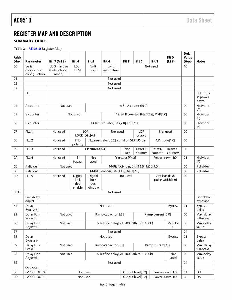
AD9510 Data Sheet
Rev. C | Page 44 of 56
REGISTER MAP AND DESCRIPTION SUMMARY TABLE
Table 24. AD9510 Register Map
Addr (Hex) Parameter Bit 7 (MSB) Bit 6 Bit 5 Bit 4 Bit 3 Bit 2 Bit 1
Bit 0 (LSB)
Def. Value (Hex) Notes
00 Serial control port configuration
SDO inactive (bidirectional
mode)
LSB_ FIRST
Soft reset
Long instruction
Not used 10
01 Not used 02 Not used 03 Not used PLL PLL starts
in power-down
04 A counter Not used 6-Bit A counter[5:0] 00 N divider (A)
05 B counter Not used 13-Bit B counter, Bits[12:8], MSB[4:0] 00 N divider (B)
06 B counter 13-Bit B counter, Bits[7:0], LSB[7:0] 00 N divider (B)
07 PLL 1 Not used LOR LOCK_DEL[6:5]
Not used LOR enable
Not used 00
08 PLL 2 Not used PFD polarity
PLL mux select[5:2] signal on STATUS pin CP mode[1:0] 00
09 PLL 3 Not used CP current[6:4] Not used
Reset R counter
Reset N counter
Reset All counters
00
0A PLL 4 Not used B bypass
Not used
Prescaler P[4:2] Power-down[1:0] 01 N divider (P)
0B R divider Not used 14-Bit R divider, Bits[13:8], MSB[5:0] 00 R divider 0C R divider 14-Bit R divider, Bits[13:8], MSB[7:0] 00 R divider 0D PLL 5 Not used Digital
lock det.
enable
Digital lock det.
window
Not used Antibacklash pulse width[1:0]
00
0E33 Not used Fine delay
adjust Fine delays
bypassed 34 Delay
Bypass 5 Not used Bypass 01 Bypass
delay 35 Delay Full-
Scale 5 Not used Ramp capacitor[5:3] Ramp current [2:0] 00 Max. delay
full-scale 36 Delay Fine
Adjust 5 Not used 5-bit fine delay[5:1] (00000b to 11000b) Must be
0 00 Min. delay
value 37 Not used 04 38 Delay
Bypass 6 Not used Bypass 01 Bypass
delay 39 Delay Full-
Scale 6 Not used Ramp capacitor[5:3] Ramp current[2:0] 00 Max. delay
full-scale 3A Delay Fine
Adjust 6 Not used 5-bit fine delay[5:1] (00000b to 11000b) Not
used 00 Min. delay
value 3B Not used 04 Outputs 3C LVPECL OUT0 Not used Output level[3:2] Power-down[1:0] 0A Off 3D LVPECL OUT1 Not used Output level[3:2] Power-down[1:0] 08 On
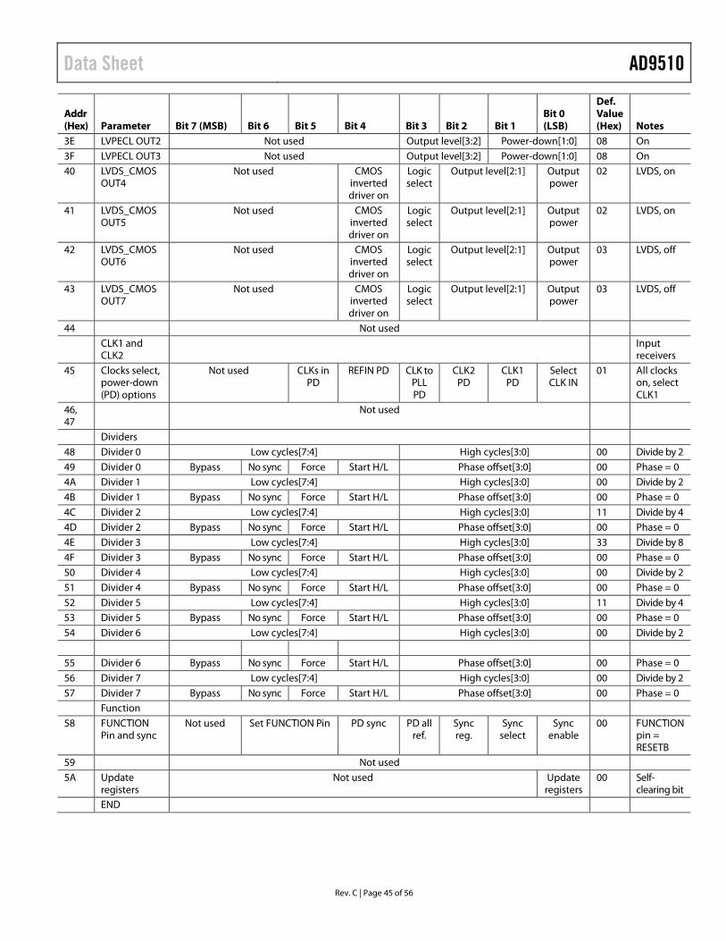
Data Sheet AD9510
Rev. C | Page 45 of 56
Addr (Hex) Parameter Bit 7 (MSB) Bit 6 Bit 5 Bit 4 Bit 3 Bit 2 Bit 1
Bit 0 (LSB)
Def. Value (Hex) Notes
3E LVPECL OUT2 Not used Output level[3:2] Power-down[1:0] 08 On 3F LVPECL OUT3 Not used Output level[3:2] Power-down[1:0] 08 On 40 LVDS_CMOS
OUT4 Not used CMOS
inverted driver on
Logic select
Output level[2:1] Output power
02 LVDS, on
41 LVDS_CMOS OUT5
Not used CMOS inverted driver on
Logic select
Output level[2:1] Output power
02 LVDS, on
42 LVDS_CMOS OUT6
Not used CMOS inverted driver on
Logic select
Output level[2:1] Output power
03 LVDS, off
43 LVDS_CMOS OUT7
Not used CMOS inverted driver on
Logic select
Output level[2:1] Output power
03 LVDS, off
44 Not used CLK1 and
CLK2 Input
receivers 45 Clocks select,
power-down (PD) options
Not used CLKs in PD
REFIN PD CLK to PLL PD
CLK2 PD
CLK1 PD
Select CLK IN
01 All clocks on, select CLK1
46, 47
Not used
Dividers 48 Divider 0 Low cycles[7:4] High cycles[3:0] 00 Divide by 2 49 Divider 0 Bypass No sync Force Start H/L Phase offset[3:0] 00 Phase = 0 4A Divider 1 Low cycles[7:4] High cycles[3:0] 00 Divide by 2 4B Divider 1 Bypass No sync Force Start H/L Phase offset[3:0] 00 Phase = 0 4C Divider 2 Low cycles[7:4] High cycles[3:0] 11 Divide by 4 4D Divider 2 Bypass No sync Force Start H/L Phase offset[3:0] 00 Phase = 0 4E Divider 3 Low cycles[7:4] High cycles[3:0] 33 Divide by 8 4F Divider 3 Bypass No sync Force Start H/L Phase offset[3:0] 00 Phase = 0 50 Divider 4 Low cycles[7:4] High cycles[3:0] 00 Divide by 2 51 Divider 4 Bypass No sync Force Start H/L Phase offset[3:0] 00 Phase = 0 52 Divider 5 Low cycles[7:4] High cycles[3:0] 11 Divide by 4 53 Divider 5 Bypass No sync Force Start H/L Phase offset[3:0] 00 Phase = 0 54 Divider 6 Low cycles[7:4] High cycles[3:0] 00 Divide by 2 55 Divider 6 Bypass No sync Force Start H/L Phase offset[3:0] 00 Phase = 0 56 Divider 7 Low cycles[7:4] High cycles[3:0] 00 Divide by 2 57 Divider 7 Bypass No sync Force Start H/L Phase offset[3:0] 00 Phase = 0 Function 58 FUNCTION
Pin and sync Not used Set FUNCTION Pin PD sync PD all
ref. Sync reg.
Sync select
Sync enable
00 FUNCTION pin = RESETB
59 Not used 5A Update
registers Not used Update
registers 00 Self-
clearing bit END
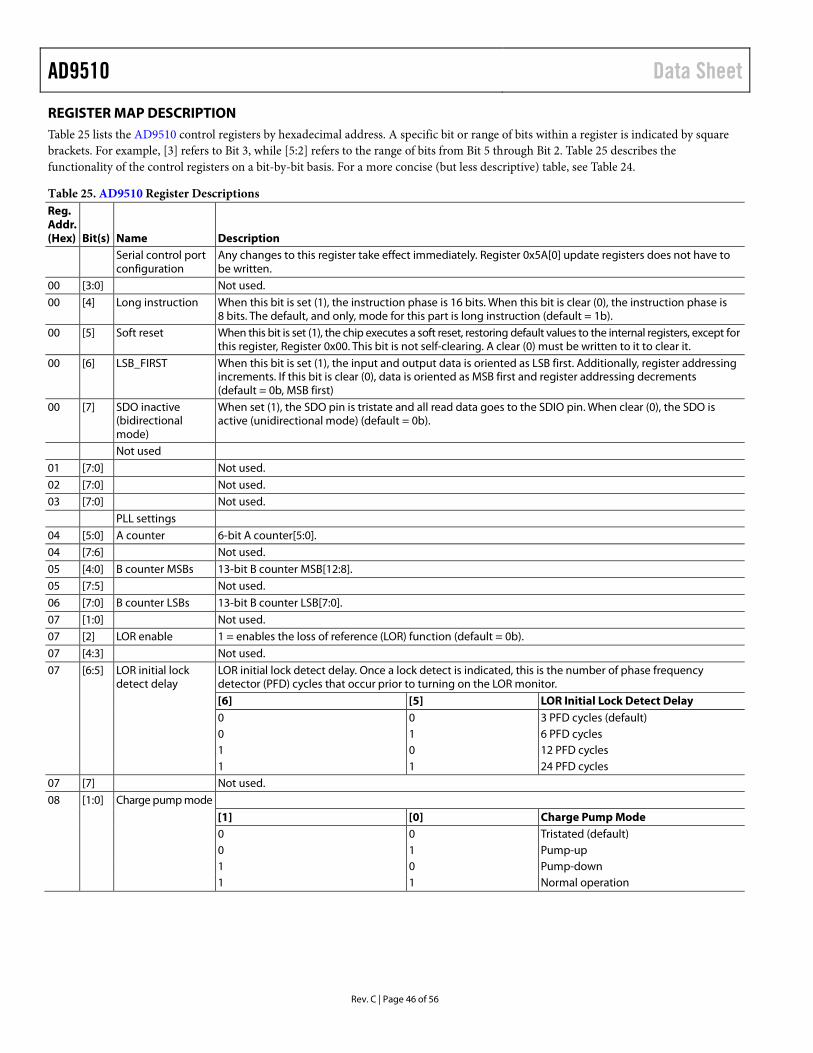
AD9510 Data Sheet
Rev. C | Page 46 of 56
REGISTER MAP DESCRIPTION Table 25 lists the AD9510 control registers by hexadecimal address. A specific bit or range of bits within a register is indicated by square brackets. For example, [3] refers to Bit 3, while [5:2] refers to the range of bits from Bit 5 through Bit 2. Table 25 describes the functionality of the control registers on a bit-by-bit basis. For a more concise (but less descriptive) table, see Table 24.
Table 25. AD9510 Register Descriptions Reg. Addr. (Hex) Bit(s) Name Description Serial control port
configuration Any changes to this register take effect immediately. Register 0x5A[0] update registers does not have to be written.
00 [3:0] Not used. 00 [4] Long instruction When this bit is set (1), the instruction phase is 16 bits. When this bit is clear (0), the instruction phase is
8 bits. The default, and only, mode for this part is long instruction (default = 1b). 00 [5] Soft reset When this bit is set (1), the chip executes a soft reset, restoring default values to the internal registers, except for
this register, Register 0x00. This bit is not self-clearing. A clear (0) must be written to it to clear it. 00 [6] LSB_FIRST When this bit is set (1), the input and output data is oriented as LSB first. Additionally, register addressing
increments. If this bit is clear (0), data is oriented as MSB first and register addressing decrements (default = 0b, MSB first)
00 [7] SDO inactive (bidirectional mode)
When set (1), the SDO pin is tristate and all read data goes to the SDIO pin. When clear (0), the SDO is active (unidirectional mode) (default = 0b).
Not used 01 [7:0] Not used. 02 [7:0] Not used. 03 [7:0] Not used. PLL settings 04 [5:0] A counter 6-bit A counter[5:0]. 04 [7:6] Not used. 05 [4:0] B counter MSBs 13-bit B counter MSB[12:8]. 05 [7:5] Not used. 06 [7:0] B counter LSBs 13-bit B counter LSB[7:0]. 07 [1:0] Not used. 07 [2] LOR enable 1 = enables the loss of reference (LOR) function (default = 0b). 07 [4:3] Not used. 07 [6:5] LOR initial lock
detect delay LOR initial lock detect delay. Once a lock detect is indicated, this is the number of phase frequency detector (PFD) cycles that occur prior to turning on the LOR monitor.
[6] [5] LOR Initial Lock Detect Delay 0 0 3 PFD cycles (default) 0 1 6 PFD cycles 1 0 12 PFD cycles 1 1 24 PFD cycles 07 [7] Not used. 08 [1:0] Charge pump mode [1] [0] Charge Pump Mode 0 0 Tristated (default) 0 1 Pump-up 1 0 Pump-down 1 1 Normal operation
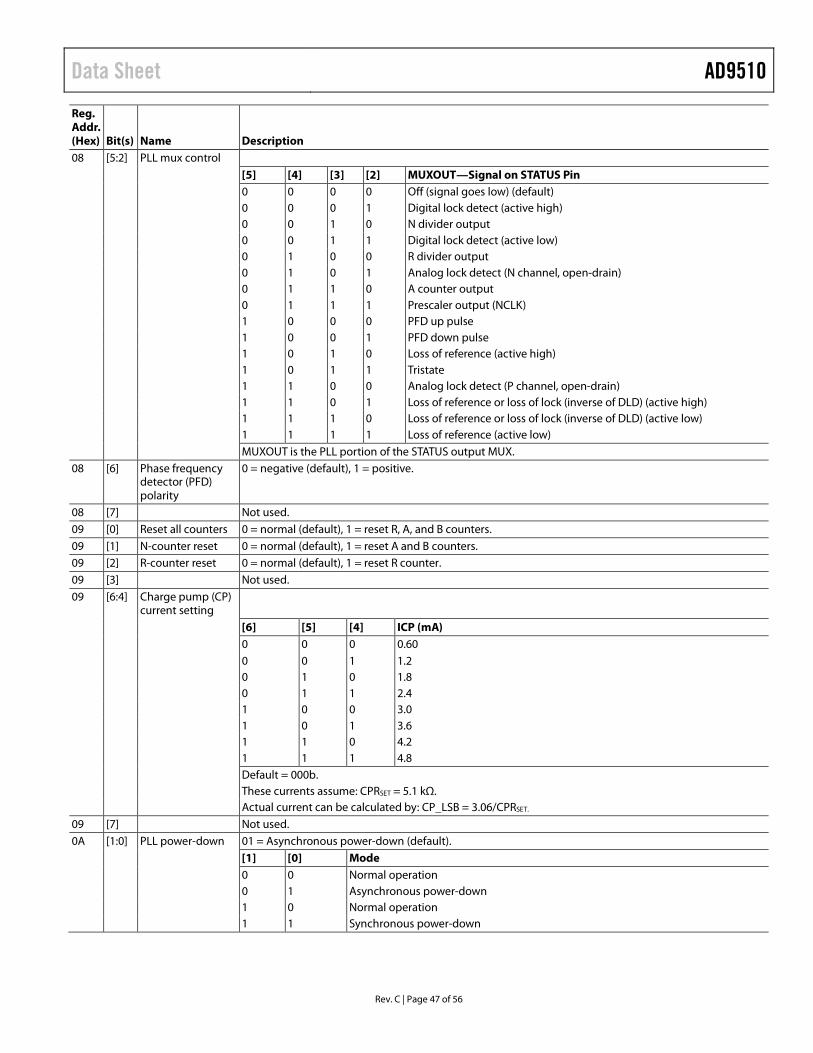
Data Sheet AD9510
Rev. C | Page 47 of 56
Reg. Addr. (Hex) Bit(s) Name Description 08 [5:2] PLL mux control [5] [4] [3] [2] MUXOUT—Signal on STATUS Pin 0 0 0 0 Off (signal goes low) (default) 0 0 0 1 Digital lock detect (active high) 0 0 1 0 N divider output 0 0 1 1 Digital lock detect (active low) 0 1 0 0 R divider output 0 1 0 1 Analog lock detect (N channel, open-drain) 0 1 1 0 A counter output 0 1 1 1 Prescaler output (NCLK) 1 0 0 0 PFD up pulse 1 0 0 1 PFD down pulse 1 0 1 0 Loss of reference (active high) 1 0 1 1 Tristate 1 1 0 0 Analog lock detect (P channel, open-drain) 1 1 0 1 Loss of reference or loss of lock (inverse of DLD) (active high) 1 1 1 0 Loss of reference or loss of lock (inverse of DLD) (active low) 1 1 1 1 Loss of reference (active low) MUXOUT is the PLL portion of the STATUS output MUX. 08 [6] Phase frequency
detector (PFD) polarity
0 = negative (default), 1 = positive.
08 [7] Not used. 09 [0] Reset all counters 0 = normal (default), 1 = reset R, A, and B counters. 09 [1] N-counter reset 0 = normal (default), 1 = reset A and B counters. 09 [2] R-counter reset 0 = normal (default), 1 = reset R counter. 09 [3] Not used. 09 [6:4] Charge pump (CP)
current setting
[6] [5] [4] ICP (mA) 0 0 0 0.60 0 0 1 1.2 0 1 0 1.8 0 1 1 2.4 1 0 0 3.0 1 0 1 3.6 1 1 0 4.2 1 1 1 4.8 Default = 000b. These currents assume: CPRSET = 5.1 kΩ. Actual current can be calculated by: CP_LSB = 3.06/CPRSET. 09 [7] Not used. 0A [1:0] PLL power-down 01 = Asynchronous power-down (default). [1] [0] Mode 0 0 Normal operation 0 1 Asynchronous power-down 1 0 Normal operation 1 1 Synchronous power-down
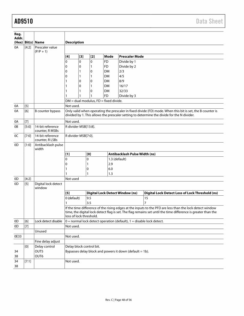
AD9510 Data Sheet
Rev. C | Page 48 of 56
Reg. Addr. (Hex) Bit(s) Name Description 0A [4:2] Prescaler value
(P/P + 1)
[4] [3] [2] Mode Prescaler Mode 0 0 0 FD Divide by 1 0 0 1 FD Divide by 2 0 1 0 DM 2/3 0 1 1 DM 4/5 1 0 0 DM 8/9 1 0 1 DM 16/17 1 1 0 DM 32/33 1 1 1 FD Divide by 3 DM = dual modulus, FD = fixed divide. 0A [5] Not used. 0A [6] B counter bypass Only valid when operating the prescaler in fixed divide (FD) mode. When this bit is set, the B counter is
divided by 1. This allows the prescaler setting to determine the divide for the N divider.
0A [7] Not used. 0B [5:0] 14-bit reference
counter, R MSBs R divider MSB[13:8].
0C [7:0] 14-bit reference counter, R LSBs
R divider MSB[7:0].
0D [1:0] Antibacklash pulse width
[1] [0] Antibacklash Pulse Width (ns) 0 0 1.3 (default) 0 1 2.9 1 0 6.0 1 1 1.3 0D [4:2] Not used 0D [5] Digital lock detect
window
[5] Digital Lock Detect Window (ns) Digital Lock Detect Loss of Lock Threshold (ns) 0 (default) 9.5 15 1 3.5 7 If the time difference of the rising edges at the inputs to the PFD are less than the lock detect window
time, the digital lock detect flag is set. The flag remains set until the time difference is greater than the loss of lock threshold.
0D [6] Lock detect disable 0 = normal lock detect operation (default), 1 = disable lock detect. 0D [7] Not used. Unused 0E33 Not used. Fine delay adjust [0] Delay control Delay block control bit. 34 OUT5 Bypasses delay block and powers it down (default = 1b). 38 OUT6 34 [7:1] Not used. 38

Data Sheet AD9510
Rev. C | Page 49 of 56
Reg. Addr. (Hex) Bit(s) Name Description [2:0] Ramp current 35 OUT5 The slowest ramp (200 µA) sets the longest full scale of approximately 10 ns. 39 OUT6 [2] [1] [0] Ramp Current (µA) 0 0 0 200 0 0 1 400 0 1 0 600 0 1 1 800 1 0 0 1000 1 0 1 1200 1 1 0 1400 1 1 1 1600 [5:3] Ramp capacitor Selects the number of capacitors in ramp generation circuit. 35 OUT5 More capacitors → slower ramp. 39 OUT6 [5] [4] [3] Number of Capacitors 0 0 0 4 (default) 0 0 1 3 0 1 0 3 0 1 1 2 1 0 0 3 1 0 1 2 1 1 0 2 1 1 1 1 [5:1] Delay fine adjust 36 OUT5 Sets delay within full scale of the ramp; there are 25 steps. 3A OUT6 00000 → zero delay (default). 11000 → maximum delay. 3C [1:0] Power-down
LVPECL
3D OUT0 3E OUT1 3F OUT2 OUT3 Mode [1] [0] Description Output On 0 0 Normal operation. On PD1 0 1 Test only—do not use. Off PD2 1 0 Safe power-down. Partial power-down; use if output
has load resistors. Off
PD3 1 1 Total power-down. Use only if output has no load resistors.
Off
3C [3:2] Output level LVPECL 3D OUT0 Output single-ended voltage levels for LVPECL outputs. 3E OUT1 3F OUT2 OUT3 [3] [2] Output Voltage (mV) 0 0 500 0 1 340 1 0 810 (default) 1 1 660
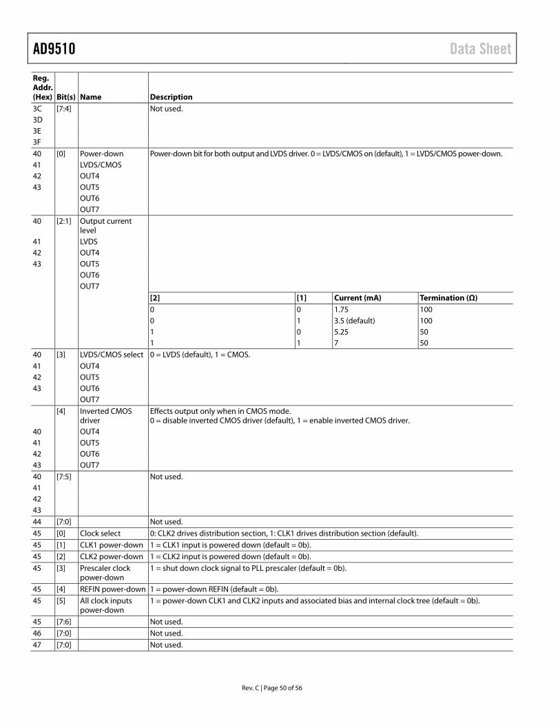
AD9510 Data Sheet
Rev. C | Page 50 of 56
Reg. Addr. (Hex) Bit(s) Name Description 3C [7:4] Not used. 3D 3E 3F 40 [0] Power-down Power-down bit for both output and LVDS driver. 0 = LVDS/CMOS on (default), 1 = LVDS/CMOS power-down. 41 LVDS/CMOS 42 OUT4 43 OUT5 OUT6 OUT7 40 [2:1] Output current
level
41 LVDS 42 OUT4 43 OUT5 OUT6 OUT7 [2] [1] Current (mA) Termination (Ω) 0 0 1.75 100 0 1 3.5 (default) 100 1 0 5.25 50 1 1 7 50 40 [3] LVDS/CMOS select 0 = LVDS (default), 1 = CMOS. 41 OUT4 42 OUT5 43 OUT6 OUT7 [4] Inverted CMOS
driver Effects output only when in CMOS mode. 0 = disable inverted CMOS driver (default), 1 = enable inverted CMOS driver.
40 OUT4 41 OUT5 42 OUT6 43 OUT7 40 [7:5] Not used. 41 42 43 44 [7:0] Not used. 45 [0] Clock select 0: CLK2 drives distribution section, 1: CLK1 drives distribution section (default). 45 [1] CLK1 power-down 1 = CLK1 input is powered down (default = 0b). 45 [2] CLK2 power-down 1 = CLK2 input is powered down (default = 0b). 45 [3] Prescaler clock
power-down 1 = shut down clock signal to PLL prescaler (default = 0b).
45 [4] REFIN power-down 1 = power-down REFIN (default = 0b). 45 [5] All clock inputs
power-down 1 = power-down CLK1 and CLK2 inputs and associated bias and internal clock tree (default = 0b).
45 [7:6] Not used. 46 [7:0] Not used. 47 [7:0] Not used.
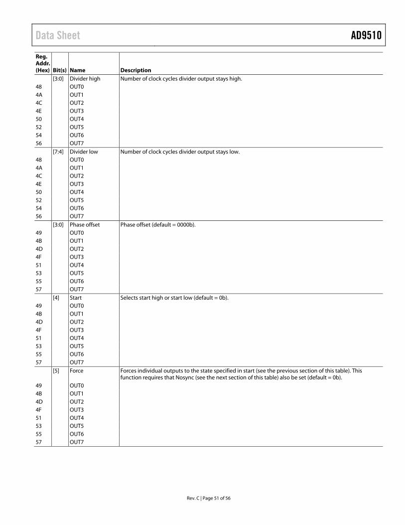
Data Sheet AD9510
Rev. C | Page 51 of 56
Reg. Addr. (Hex) Bit(s) Name Description [3:0] Divider high Number of clock cycles divider output stays high. 48 OUT0 4A OUT1 4C OUT2 4E OUT3 50 OUT4 52 OUT5 54 OUT6 56 OUT7 [7:4] Divider low Number of clock cycles divider output stays low. 48 OUT0 4A OUT1 4C OUT2 4E OUT3 50 OUT4 52 OUT5 54 OUT6 56 OUT7 [3:0] Phase offset Phase offset (default = 0000b). 49 OUT0 4B OUT1 4D OUT2 4F OUT3 51 OUT4 53 OUT5 55 OUT6 57 OUT7 [4] Start Selects start high or start low (default = 0b). 49 OUT0 4B OUT1 4D OUT2 4F OUT3 51 OUT4 53 OUT5 55 OUT6 57 OUT7 [5] Force Forces individual outputs to the state specified in start (see the previous section of this table). This
function requires that Nosync (see the next section of this table) also be set (default = 0b). 49 OUT0 4B OUT1 4D OUT2 4F OUT3 51 OUT4 53 OUT5 55 OUT6 57 OUT7

AD9510 Data Sheet
Rev. C | Page 52 of 56
Reg. Addr. (Hex) Bit(s) Name Description [6] Nosync Ignore chip-level sync signal (default = 0b). 49 OUT0 4B OUT1 4D OUT2 4F OUT3 51 OUT4 53 OUT5 55 OUT6 57 OUT7 [7] Bypass divider Bypass and power down divider logic; route clock directly to output (default = 0b). 49 OUT0 4B OUT1 4D OUT2 4F OUT3 51 OUT4 53 OUT5 55 OUT6 57 OUT7 58 [0] SYNC detect enable 1 = enable SYNC detect (default = 0b).
58 [1] SYNC select 1 = raise flag if slow clocks are out-of-sync by 0.5 to 1 high speed clock cycles. 0 (default) = raise flag if slow clocks are out-of-sync by 1 to 1.5 high speed clock cycles.
58 [2] Soft SYNC The Soft SYNC bit works the same as the FUNCTION pin when in SYNCB mode, except that the polarity of this bit is reversed. That is, a high level forces selected outputs into a known state, and a high > low transition triggers a sync (default = 0b).
58 [3] Dist ref power-down
1 = power down the references for the distribution section (default = 0b).
58 [4] SYNC power-down 1 = power down the SYNC (default = 0b).
58 [6:5] FUNCTION pin select
[6] [5] Function 0 0 RESETB (default) 0 1 SYNCB 1 0 Test only, do not use 1 1 PDB 58 [7] Not used. 59 [7:0] Not used. 5A [0] Update registers Writing a 1 to this bit updates all registers and transfers all serial control port register buffer contents to
the control registers on the next rising SCLK edge. This is a self-clearing bit; a 0 does not have to be written to clear it.
5A [7:1] Not used. End
Data Sheet AD9510
Rev. C | Page 53 of 56
POWER SUPPLY The AD9510 requires a 3.3 V ± 5% power supply for VS. The tables in the Specifications section give the performance expected from the AD9510 with the power supply voltage within this range. The absolute maximum range of −0.3 V − +3.6 V, with respect to GND, must never be exceeded on the VS pin.
Follow good engineering practice in the layout of power supply traces and the ground plane of the printed circuit board (PCB). Bypass the power supply on the PCB with adequate capacitance (>10 µF). Bypass the AD9510 with adequate capacitors (0.1 µF) at all power pins as close as possible to the part. The layout of the AD9510 evaluation board (AD9510/PCBZ or AD9510-VCO/PCBZ) is a good example.
The AD9510 is a complex part that is programmed for its desired operating configuration by on-chip registers. These registers are not maintained over a shutdown of external power. This means that the registers can lose their programmed values if VS is lost long enough for the internal voltages to collapse. Careful bypassing protects the part from memory loss under normal conditions. Nonetheless, it is important that the VS power supply not become intermittent, or the AD9510 risks losing its programming.
The internal bias currents of the AD9510 are set by the RSET and CPRSET resistors. These resistors must be as close as possible to the values given as conditions in the Specifications section (RSET = 4.12 kΩ and CPRSET = 5.1 kΩ). These values are standard 1% resistor values, and are readily obtainable. The bias currents set by these resistors determine the logic levels and operating conditions of the internal blocks of the AD9510. The performance figures given in the Specifications section assume that these resistor values are used.
The VCP pin is the supply pin for the charge pump (CP). The voltage at this pin (VCP) can be from VS up to 5.5 V, as required to match the tuning voltage range of a specific VCO/VCXO. This voltage must never exceed the absolute maximum of 6 V. Additionally, never allow VCP to be less than −0.3 V below VS or GND, whichever is lower.
The exposed metal paddle on the AD9510 package is an electrical connection, as well as a thermal enhancement. For the device to function properly, the paddle must be properly attached to ground (GND). The PCB acts as a heat sink for the AD9510; therefore, this GND connection must provide a good thermal path to a larger dissipation area, such as a ground plane on the PCB. See the layout of the AD9510 evaluation board (AD9510/PCBZ or AD9510-VCO/PCBZ) for a good example.
POWER MANAGEMENT The power usage of the AD9510 can be managed to use only the power required for the functions being used. Unused features and circuitry can be powered down to save power. The following circuit blocks can be powered down, or are powered down when not selected (see the Register Map and Description section):
• The PLL section can be powered down if not needed. • Any of the dividers are powered down when bypassed—
equivalent to divide-by-one. • The adjustable delay blocks on OUT5 and OUT6 are
powered down when not selected. • Any output can be powered down. However, LVPECL
outputs have both a safe and an off condition. When the LVPECL output is terminated, use only the safe shutdown to protect the LVPECL output devices. This still consumes some power.
• The entire distribution section can be powered down when not needed.
Powering down a functional block does not cause the program-ming information for that block (in the registers) to be lost. This means that blocks can be powered on and off without otherwise having to reprogram the AD9510. However, synchro-nization is lost. A SYNC must be issued to resynchronize (see the Single-Chip Synchronization section).
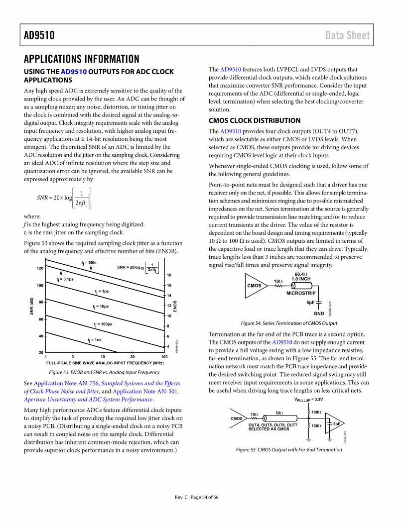
AD9510 Data Sheet
Rev. C | Page 54 of 56
APPLICATIONS INFORMATION USING THE AD9510 OUTPUTS FOR ADC CLOCK APPLICATIONS Any high speed ADC is extremely sensitive to the quality of the sampling clock provided by the user. An ADC can be thought of as a sampling mixer; any noise, distortion, or timing jitter on the clock is combined with the desired signal at the analog-to-digital output. Clock integrity requirements scale with the analog input frequency and resolution, with higher analog input fre-quency applications at ≥ 14-bit resolution being the most stringent. The theoretical SNR of an ADC is limited by the ADC resolution and the jitter on the sampling clock. Considering an ideal ADC of infinite resolution where the step size and quantization error can be ignored, the available SNR can be expressed approximately by
×=
jftSNR
2π1log20
where: f is the highest analog frequency being digitized. tj is the rms jitter on the sampling clock.
Figure 53 shows the required sampling clock jitter as a function of the analog frequency and effective number of bits (ENOB).
Figure 53. ENOB and SNR vs. Analog Input Frequency
See Application Note AN-756, Sampled Systems and the Effects of Clock Phase Noise and Jitter, and Application Note AN-501, Aperture Uncertainty and ADC System Performance.
Many high performance ADCs feature differential clock inputs to simplify the task of providing the required low jitter clock on a noisy PCB. (Distributing a single-ended clock on a noisy PCB can result in coupled noise on the sample clock. Differential distribution has inherent common-mode rejection, which can provide superior clock performance in a noisy environment.)
The AD9510 features both LVPECL and LVDS outputs that provide differential clock outputs, which enable clock solutions that maximize converter SNR performance. Consider the input requirements of the ADC (differential or single-ended, logic level, termination) when selecting the best clocking/converter solution.
CMOS CLOCK DISTRIBUTION The AD9510 provides four clock outputs (OUT4 to OUT7), which are selectable as either CMOS or LVDS levels. When selected as CMOS, these outputs provide for driving devices requiring CMOS level logic at their clock inputs.
Whenever single-ended CMOS clocking is used, follow some of the following general guidelines.
Point-to-point nets must be designed such that a driver has one receiver only on the net, if possible. This allows for simple termina-tion schemes and minimizes ringing due to possible mismatched impedances on the net. Series termination at the source is generally required to provide transmission line matching and/or to reduce current transients at the driver. The value of the resistor is dependent on the board design and timing requirements (typically 10 Ω to 100 Ω is used). CMOS outputs are limited in terms of the capacitive load or trace length that they can drive. Typically, trace lengths less than 3 inches are recommended to preserve signal rise/fall times and preserve signal integrity.
Figure 54. Series Termination of CMOS Output
Termination at the far end of the PCB trace is a second option. The CMOS outputs of the AD9510 do not supply enough current to provide a full voltage swing with a low impedance resistive, far-end termination, as shown in Figure 55. The far-end termi-nation network must match the PCB trace impedance and provide the desired switching point. The reduced signal swing may still meet receiver input requirements in some applications. This can be useful when driving long trace lengths on less critical nets.
Figure 55. CMOS Output with Far-End Termination
120
100
80
60
40
204
6
8
10
12
14
16
18
1 3 10 30 100
0504
6-02
4
FULL-SCALE SINE WAVE ANALOG INPUT FREQUENCY (MHz)
SNR
(dB
)
ENO
B
tj = 50fs
tj = 0.1ps
tj = 1ps
tj = 10ps
tj = 100ps
tj = 1ns
SNR = 20log101
2πftj
0504
6-02
5
10Ω
MICROSTRIP
GND
5pF
60.4Ω1.0 INCH
CMOS
0504
6-02
7
50Ω10Ω
OUT4, OUT5, OUT6, OUT7SELECTED AS CMOS
VPULLUP = 3.3V
CMOS3pF
100Ω
100Ω
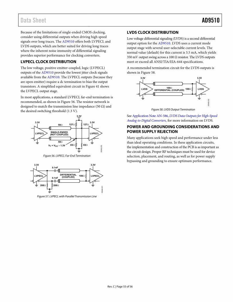
Data Sheet AD9510
Rev. C | Page 55 of 56
Because of the limitations of single-ended CMOS clocking, consider using differential outputs when driving high speed signals over long traces. The AD9510 offers both LVPECL and LVDS outputs, which are better suited for driving long traces where the inherent noise immunity of differential signaling provides superior performance for clocking converters.
LVPECL CLOCK DISTRIBUTION The low voltage, positive emitter-coupled, logic (LVPECL) outputs of the AD9510 provide the lowest jitter clock signals available from the AD9510. The LVPECL outputs (because they are open emitter) require a dc termination to bias the output transistors. A simplified equivalent circuit in Figure 41 shows the LVPECL output stage.
In most applications, a standard LVPECL far-end termination is recommended, as shown in Figure 56. The resistor network is designed to match the transmission line impedance (50 Ω) and the desired switching threshold (1.3 V).
Figure 56. LVPECL Far-End Termination
Figure 57. LVPECL with Parallel Transmission Line
LVDS CLOCK DISTRIBUTION Low voltage differential signaling (LVDS) is a second differential output option for the AD9510. LVDS uses a current mode output stage with several user-selectable current levels. The normal value (default) for this current is 3.5 mA, which yields 350 mV output swing across a 100 Ω resistor. The LVDS outputs meet or exceed all ANSI/TIA/EIA-644 specifications.
A recommended termination circuit for the LVDS outputs is shown in Figure 58.
Figure 58. LVDS Output Termination
See Application Note AN-586, LVDS Data Outputs for High-Speed Analog-to-Digital Converters, for more information on LVDS.
POWER AND GROUNDING CONSIDERATIONS AND POWER SUPPLY REJECTION Many applications seek high speed and performance under less than ideal operating conditions. In these application circuits, the implementation and construction of the PCB is as important as the circuit design. Proper RF techniques must be used for device selection, placement, and routing, as well as for power supply bypassing and grounding to ensure optimum performance.
0504
6-03
0
3.3V
LVPECL
50Ω
50Ω
SINGLE-ENDED(NOT COUPLED)
3.3V
3.3V
LVPECL
127Ω127Ω
83Ω83ΩVT = VCC – 1.3V
0504
6-03
1
3.3V
LVPECL DIFFERENTIAL(COUPLED)
3.3V
LVPECL100Ω0.1nF
0.1nF
200Ω 200Ω
0504
6-03
2
3.3V
LVDS 100ΩDIFFERENTIAL (COUPLED)
3.3V
LVDS100Ω
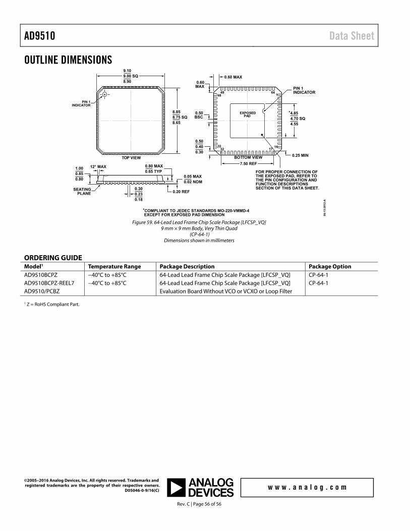
AD9510 Data Sheet
Rev. C | Page 56 of 56
OUTLINE DIMENSIONS
Figure 59. 64-Lead Lead Frame Chip Scale Package [LFCSP_VQ] 9 mm × 9 mm Body, Very Thin Quad
(CP-64-1) Dimensions shown in millimeters
ORDERING GUIDE Model1 Temperature Range Package Description Package Option AD9510BCPZ −40°C to +85°C 64-Lead Lead Frame Chip Scale Package [LFCSP_VQ] CP-64-1 AD9510BCPZ-REEL7 −40°C to +85°C 64-Lead Lead Frame Chip Scale Package [LFCSP_VQ] CP-64-1 AD9510/PCBZ Evaluation Board Without VCO or VCXO or Loop Filter
1 Z = RoHS Compliant Part.
*COMPLIANT TO JEDEC STANDARDS MO-220-VMMD-4 EXCEPT FOR EXPOSED PAD DIMENSION
0.25 MIN
164
1617
4948
3233
0.500.400.30
0.50BSC
0.20 REF
12° MAX 0.80 MAX0.65 TYP
1.000.850.80
7.50 REF
0.05 MAX0.02 NOM
0.60 MAX0.60
MAX
SEATINGPLANE
PIN 1INDICATOR
*4.854.70 SQ4.55
PIN 1INDICATOR
0.300.230.18
FOR PROPER CONNECTION OFTHE EXPOSED PAD, REFER TOTHE PIN CONFIGURATION ANDFUNCTION DESCRIPTIONSSECTION OF THIS DATA SHEET.
TOP VIEW
EXPOSEDPAD
BOTTOM VIEW
9.109.00 SQ8.90
8.858.75 SQ8.65
06
-13
-20
12-A
©2005–2016 Analog Devices, Inc. All rights reserved. Trademarks and registered trademarks are the property of their respective owners.
D05046-0-9/16(C)