1.3 highly resistive substrate cmos on soi for wireless front-end switch...
TRANSCRIPT
Highly Resistive Substrate CMOS on SOI for Wireless Front-End Switch Applications
Randy Wolf1*, Dawn Wang2, Alvin Joseph1, Alan Botula1,
Peter Rabbeni1, David Harame1 and Jim Dunn1
1 IBM, 1000 River St, Essex Junction, VT 05452, USA 2 IBM, 5 Technology Park Dr, Westford, MA 01886, USA *Email: [email protected], Phone: +1 802 769 0816
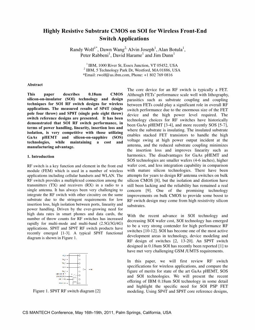
Abstract This paper describes 0.18um CMOS silicon-on-insulator (SOI) technology and design techniques for SOI RF switch designs for wireless applications. The measured results of SP4T (single pole four throw) and SP8T (single pole eight throw) switch reference designs are presented. It has been demonstrated that SOI RF switch performance, in terms of power handling, linearity, insertion loss and isolation, is very competitive with those utilizing GaAs pHEMT and silicon-on-sapphire (SOS) technologies, while maintaining a cost and manufacturing advantage. 1. Introduction RF switch is a key function and element in the front end module (FEM) which is used in a number of wireless applications including cellular handsets and WLAN. The RF switch provides a multiplexed connection among the transmitters (TX) and receivers (RX) in a radio to a single antenna. It has always been very challenging to integrate the RF switch with other circuitry on the same substrate due to the stringent requirements for low insertion loss, high isolation between ports, linearity and power handling. Driven by the ever-growing need for high data rates in smart phones and data cards, the number of throw counts for RF switches has increased rapidly for multi-mode and multi-band (2.5G/3G/4G) applications. SP8T and SP9T RF switch products have recently emerged [1-3]. A typical SP8T functional diagram is shown in Figure 1.
Figure 1. SP8T RF switch diagram [2]
The core device for an RF switch is typically a FET. Although FETs’ performance scale well with lithography, parasitics such as substrate coupling and coupling between FETs could play a significant role in overall RF switch performance due to the enormous size of the FET device and the high power level required. The technology choices for RF switches have historically been GaAs pHEMT [3-4], and more recently SOS [5-7], where the substrate is insulating. The insulated substrate enables stacked FET transistors to handle the high voltage swing at high power output incident at the antenna, and the reduced substrate coupling minimizes the insertion loss and improves linearity such as harmonics. The disadvantages for GaAs pHEMT and SOS technologies are smaller wafers (4-6 inches), higher wafer cost, and less integration capability in comparison with mature silicon technologies. There have been attempts for years to design RF antenna switches on bulk silicon CMOS [8], but the isolation and distortion have still been lacking and the reliability has remained a real concern [9]. One of the promising technology improvements on bulk CMOS to provide some boost to RF switch design may come from high resistivity silicon substrates. With the recent advance in SOI technology and decreasing SOI wafer cost, SOI technology has emerged to be a very strong contender for high performance RF switches [10-12]. SOI has become one of the most active development areas in technology, device modeling and RF design of switches [2, 13-20]. An SP9T switch designed in 0.18um SOI has recently been reported [1] to have met very challenging GSM /UMTS requirements. In this paper, we will first review RF switch specifications for wireless applications, and compare the figure of merits for state of the art GaAs pHEMT, SOS and SOI technologies. We will present the recent offering of IBM 0.18um SOI technology in some detail and highlight the specific need for SOI PSP FET modeling. Using SP4T and SP8T core reference designs,
1
11CS MANTECH Conference, May 16th-19th, 2011, Palm Springs, California, USA
we will discuss the design techniques and trade-offs using SOI FETs. Finally, the measured performance of these switches will be presented. 2. CMOS SOI Technology for RF Switches In order to understand the technology requirements for RF switches, it is very helpful to start with a good understanding of RF switch specifications. The key requirements of RF antenna switches for various wireless standards are listed in Table 1.
Table 1. RF Antenna Switch Key Requirements
Insertion loss (IL) is an important metric since the RF switch is placed between the antenna and the radio, so any increase to IL translates to increased RX NF and reduced TX efficiency. High isolation between ports is required to minimize the interference or leakage from the TX to other ports. IMD (IIP2 and IIP3) and high order harmonics (2nd and 3rd) are different measures of linearity, often dealing with some out-of-band blocker effects at the system level. In GSM mode, the harmonics need to be at least -75dBc up to +35 dBm output power, which is very diffcult to achieve [1]. Switching time for WLANs is among the tightest and deserves careful design in biasing resistors [4, 19]. In addition, an RF antenna switch has to function under highly mismatched load conditions (i.e. 4:1 VSWR), as the antenna could experience unexpected impedance changes. In GSM, this implies that the peak voltage at antenna port of the RF switch could exceed 35V at maximum power output level!
2.1 Technology Benchmarking The figure of merit (FOM) commonly used for technology benchmarking in an RF switch is Ron*Coff of FET device. Ron is primarily determined by the gate channel resistance of the device during the ON state, which directly impacts the IL. Coff is dominated by the drain (D) to source (S) capacitance and gate (G) capacitances during the OFF state, which impacts the isolation. These parameters can be easily obtained through small signal measurements. In Table 2, the Ron* Coff FOM is compared among state of the art GaAs pHEMT, SOS and SOI technologies, based on the latest publications [1, 6, 11].
Table 2. Figure of Merit - Ron* Coff
Technology pHEMT
[1] SOS [6]
SOI [11]
Ldesign (um) 0.25 0.32
Ron*Coff (fs) 280 270 250
2.2 IBM 0.18um SOI Technology IBM 0.18um SOI technology has been optimized for RF switch applications [11]. The 0.18um node was selected for the RF switch platform to provide a good balance between the device voltage capability and feature size. This also has the advantage to allow porting of some of the existing devices from 0.18um bulk CMOS technology, especially for passive devices. A dual thick metal option (3um Cu /4um Al) is now available in addition to standard 4um Al final metal. A high resistivity (>750 ohm-cm) p- silicon handling wafer and 1um BOX (buried oxide) are used to minimize the capacitive coupling to the substrate. There are both partially-deleted (PD) floating body (FB) FETs and body contact (BC) FETs offered. The standard FETs are 2.5V devices with 5.2nm dual gate oxide and an Ldesign of 0.32um, with optional 1.5V FETs. The workhorse FET for RF switch design is the 2.5V dual gate NFET (dgnfet) with a breakdown of Vds greater than 3.6V [10]. In order to withstand large high voltage swings under high VSWR, stacks of 8-12 dgnfet devices are often used [21]. As all series-stacked FETs are connected in the pass gate configuration and Ron is very low, the AC voltage between the drain and source of the FETs runs across the Vds~0V point. It is known that under such a condition, the FET BSIM models (both bulk and SOI) can not accurately predict the harmonics and IMD of RF switch [14-15]. For bulk CMOS, the Philips Surface Potential (PSP) model has been adopted as an industrial standard to address this shortcoming of the BSIM model. In PD SOI FETs, there exist other specific effects such as floating body effect and gate induced drain leakage (GIDL) current. Self-heating effects also need to be considered [13-14]. To account for these effects, the PSP SOI model was jointly developed in late 2000 [12] by Arizona State University, Philips, Freescale, NXP and IBM and has been recognized to be one of the most suited models for SOI FETs for RF switch design. In order to reduce Ron, the total width of the stacked FET devices in RF switches is in the range of 2-4 mm. As a result, the wiring capacitances among these FETs can be a significant part of the total Coff. In this technology, serpentine-shaped high sheet-rho (1600 ohm /sq) resistor for biasing is offered to enable a low parasitic and area-efficient switch core layout.
12 CS MANTECH Conference, May 16th-19th, 2011, Palm Springs, California, USA
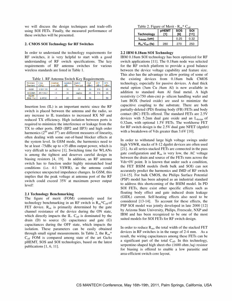
2.3 Nonlinearity in SOI Insertion loss and isolation can be easily understood using small signal analysis, and are relatively insensitive to the substrate. However, linearity, which is a large signal event, is very sensitive to the substrate. Under full power (up to +35 dBm in GSM), especially with a load mismatch, there are very high voltage swings on the gate, drain, source, body and all the inter-connecting lines. Significant levels of AC signals are coupled into the substrate to generate substrate current. In the ON mode, the linearity is mainly dominated by Ron, and the substrate current plays a lesser role, as it is much smaller than the drain current. In the OFF mode, with the high voltages on the FETs, there are also GIDL currents present due to electric fields near the S/D-to-gate/body regions. The addition of both substrate leakage and GIDL current causes an imbalance in the drain currents flowing through the long chain of FETs from the antenna. This leads to unequal division of the voltage across the stacked FETs, causing some FETs near the antenna port to become weakly turned on, causing nonlinearity [14]. Another source of substrate nonlinearity in SOI comes from the inherent C-V effect of BOX on the top of the p-type handle wafer, which acts like a CMOS capacitor, especially if the doping level of the handle wafer is not high enough [14] or there are a good amount of fixed oxide charges at the SiO2-Si interface forming an inversion layer [11, 22]. This initially had been a key impediment for SOI processes to achieve high enough harmonics performance for the GSM application. With successful process modifications, a remarkable improvement in linearity was demonstrated in both a co-planer waveguide monitor and SPST and SPDT switch cores [11-12, 20]. 3. SOI RF Switch Design The basic SOI switch topology is the same as in GaAs pHEMPT or SOS. An example of single pole double throw (SPDT) switch is illustrated in Figure 2 below. Each switch leg (TX or RX) has two branches - series (M1 or M2) and shunt (M3 or M4).
Figure 2. SPDT schematic
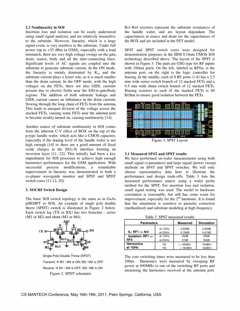
Rs1-Rs4 resistors represent the substrate resistances of the handle wafer, and are layout dependant. The capacitances at source and drain are the capacitances of the BOX and are included in the FET model. SP4T and SP8T switch cores were designed for demonstration purposes in the IBM 0.18um CMOS SOI technology described above. The layout of the SP8T is shown in Figure 3. The pads are GSG type for RF inputs with 100um pitch. On the left, labeled as RFfin, is the antenna port; on the right is the logic controller for biasing. In the middle, each of 8 RF ports (1-8) has a 2.5 mm wide series switch branch of 12 stacked FETs and a 0.5 mm wide shunt switch branch of 12 stacked FETs. Biasing resistors to each of the stacked FETs is 60 KOhm to ensure good isolation between the FETs.
Figure 3. SP8T Layout
3.1 Measured SP4T and SP8T results We have performed on-wafer measurements using both small signal (s-paramters) and large signal (power sweep) methods on SP4T and SP8T switches. We will only choose representative data here to illustrate the performance and design trade-offs. Table 3 lists the measured performance matrix using a wafer probe method for the SP8T. For insertion loss and isolation, small signal testing was used. The model to hardware correlation is reasonable, but still has some room for improvement, especially for the 2nd harmonic. It is found that the simulation is sensitive to parasitic extraction (method/tool) and substrate modeling at high frequency.
Table 3. SP8T measured results
Parameters Measured Simulation
at 1GHz 0.65dB 0.60dB IL: RF1 -> Ant at 2GHz 0.78dB 0.67dB
at 1GHz 45dB 55dB Isolation: RF1 -> RF5 at 2GHz 37dB 50dB
H2 < -45dBm -34dBm Harmonics at 1GHz H3 < -50dBm -42dBm
The core switching times were measured to be less than 200ns. Harmonics were measured by sweeping RF power at 890MHz to one of the switching RF ports and measuring the harmonics received at the antenna port.
Single-Pole Double-Throw (SPDT)
Transmit � M1 / M4 is ON; M3 / M2 is OFF
Receive � M1 / M4 is OFF; M3 / M2 is ON
1
13CS MANTECH Conference, May 16th-19th, 2011, Palm Springs, California, USA
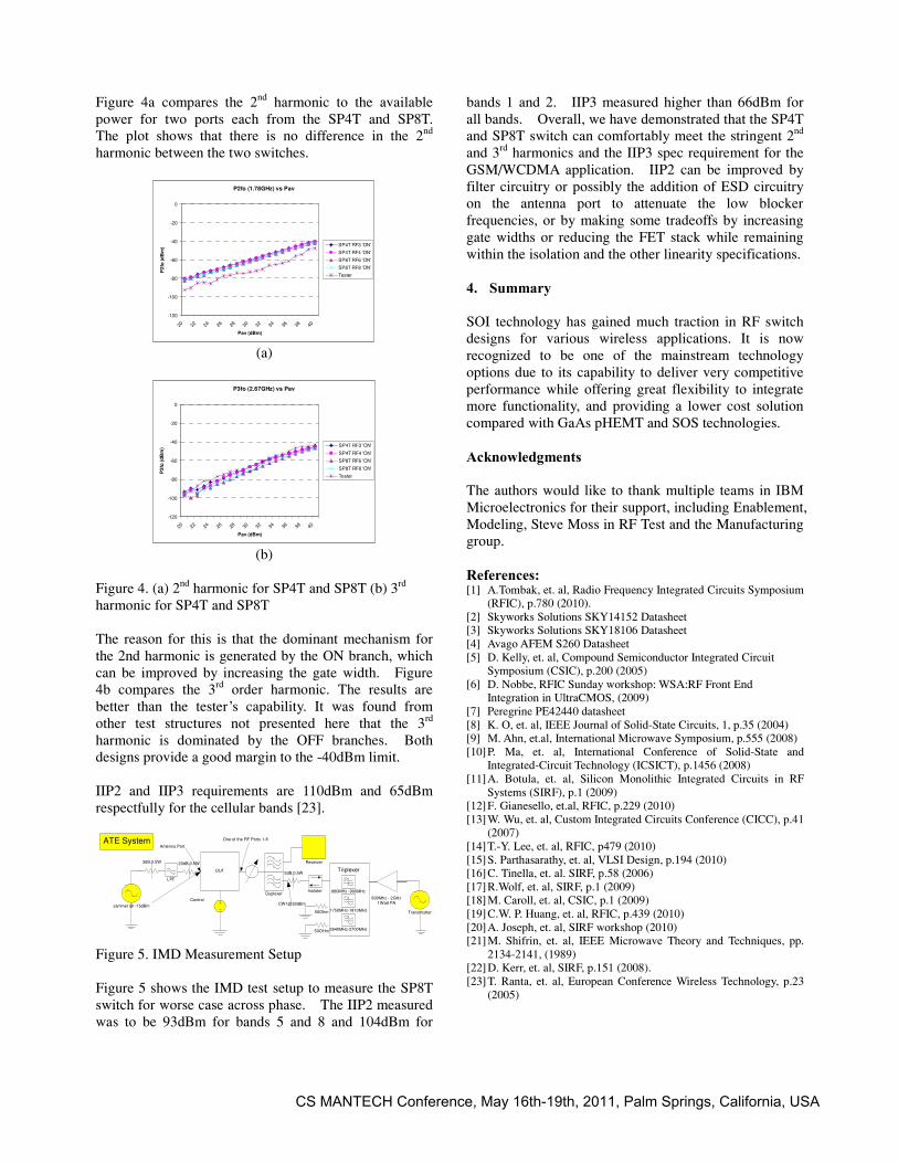
Figure 4a compares the 2nd harmonic to the available power for two ports each from the SP4T and SP8T. The plot shows that there is no difference in the 2nd harmonic between the two switches.
P2fo (1.78GHz) vs Pav
-120
-100
-80
-60
-40
-20
0
20 22 24 26 28 30 32 34 36 38 40
Pav (dBm)
P2
fo (d
Bm
) SP4T RF3 'ON'
SP4T RF4 'ON'
SP8T RF6 'ON'
SP8T RF8 'ON'
Tester
(a)
P3fo (2.67GHz) vs Pav
-120
-100
-80
-60
-40
-20
0
20 22 24 26 28 30 32 34 36 38 40
Pav (dBm)
P3f
o (d
Bm
) SP4T RF3 'ON'
SP4T RF4 'ON'
SP8T RF6 'ON'
SP8T RF8 'ON'
Tester
(b)
Figure 4. (a) 2nd harmonic for SP4T and SP8T (b) 3rd harmonic for SP4T and SP8T The reason for this is that the dominant mechanism for the 2nd harmonic is generated by the ON branch, which can be improved by increasing the gate width. Figure 4b compares the 3rd order harmonic. The results are better than the tester’s capability. It was found from other test structures not presented here that the 3rd harmonic is dominated by the OFF branches. Both designs provide a good margin to the -40dBm limit. IIP2 and IIP3 requirements are 110dBm and 65dBm respectfully for the cellular bands [23].
800Mhz - 2GHz1Watt PA
Isolator
Jammer @ -15dBm
Control
Receiver
Duplexer
DUT
Transmistter
One of the RF Ports 1-8
Antenna Port
CW1@20dBm
LPF
3dB,0.5W 20dB,0.5W
3dB,0.5W
880MHz -900MHz
1750MHz-1810MHz
2640MHz-2700MHz
Triplexer
50Ohm
50OHm
ATE System
Figure 5. IMD Measurement Setup Figure 5 shows the IMD test setup to measure the SP8T switch for worse case across phase. The IIP2 measured was to be 93dBm for bands 5 and 8 and 104dBm for
bands 1 and 2. IIP3 measured higher than 66dBm for all bands. Overall, we have demonstrated that the SP4T and SP8T switch can comfortably meet the stringent 2nd and 3rd harmonics and the IIP3 spec requirement for the GSM/WCDMA application. IIP2 can be improved by filter circuitry or possibly the addition of ESD circuitry on the antenna port to attenuate the low blocker frequencies, or by making some tradeoffs by increasing gate widths or reducing the FET stack while remaining within the isolation and the other linearity specifications. 4. Summary SOI technology has gained much traction in RF switch designs for various wireless applications. It is now recognized to be one of the mainstream technology options due to its capability to deliver very competitive performance while offering great flexibility to integrate more functionality, and providing a lower cost solution compared with GaAs pHEMT and SOS technologies. Acknowledgments The authors would like to thank multiple teams in IBM Microelectronics for their support, including Enablement, Modeling, Steve Moss in RF Test and the Manufacturing group. References: [1] A.Tombak, et. al, Radio Frequency Integrated Circuits Symposium
(RFIC), p.780 (2010). [2] Skyworks Solutions SKY14152 Datasheet [3] Skyworks Solutions SKY18106 Datasheet [4] Avago AFEM S260 Datasheet [5] D. Kelly, et. al, Compound Semiconductor Integrated Circuit
Symposium (CSIC), p.200 (2005) [6] D. Nobbe, RFIC Sunday workshop: WSA:RF Front End
Integration in UltraCMOS, (2009) [7] Peregrine PE42440 datasheet [8] K. O, et. al, IEEE Journal of Solid-State Circuits, 1, p.35 (2004) [9] M. Ahn, et.al, International Microwave Symposium, p.555 (2008) [10] P. Ma, et. al, International Conference of Solid-State and
Integrated-Circuit Technology (ICSICT), p.1456 (2008) [11] A. Botula, et. al, Silicon Monolithic Integrated Circuits in RF
Systems (SIRF), p.1 (2009) [12] F. Gianesello, et.al, RFIC, p.229 (2010) [13] W. Wu, et. al, Custom Integrated Circuits Conference (CICC), p.41
(2007) [14] T.-Y. Lee, et. al, RFIC, p479 (2010) [15] S. Parthasarathy, et. al, VLSI Design, p.194 (2010) [16] C. Tinella, et. al. SIRF, p.58 (2006) [17] R.Wolf, et. al, SIRF, p.1 (2009) [18] M. Caroll, et. al, CSIC, p.1 (2009) [19] C.W. P. Huang, et. al, RFIC, p.439 (2010) [20] A. Joseph, et. al, SIRF workshop (2010) [21] M. Shifrin, et. al, IEEE Microwave Theory and Techniques, pp.
2134-2141, (1989) [22] D. Kerr, et. al, SIRF, p.151 (2008). [23] T. Ranta, et. al, European Conference Wireless Technology, p.23
(2005)
14 CS MANTECH Conference, May 16th-19th, 2011, Palm Springs, California, USA