14. ir optical receiver ir optical receiver data sheetdlm.cypress.com.edgesuite.net/akdlm/old/spec...
TRANSCRIPT

Cypress Semiconductor Corporation • 198 Champion Court • San Jose, CA 95134-1709 • 408-943-2600Document Number: 001-13567 Rev. *D Revised February 12, 2009
14. IR Optical Receiver
Copyright © 2002-2009 Cypress Semiconductor Corporation. All Rights Reserved.
Features and Overview • Hardware implementation of IrDA receiver• Data format compliant with IrDA data format• Data bit rate selectable to a maximum receive rate of 115.2 kbps• Data framing consists of start and stop bits• Optional interrupt on receive register full• Overrun and framing error detectionThe IrDARX User Module is an 8-bit serial half-duplex receiver that supports the IrDA data format by way of an infrared data link. The data format includes a start bit, 8 data bits, and a stop bit with no parity. Flexible clocking and interrupts, on data availability, are supported. Application Programming Interface (API) firmware routines are provided to initialize, configure, and operate the Interface. A complete implementation of the IrDA protocol stack is not included. Maximum supported data rate is 115.2 kbpsidar. Additional information regarding IrDA is available at http://www.irda.org.
IR Optical Receiver Data Sheet IrDARX
ResourcesPSoC® Blocks API Memory (Bytes)
Pins Digital Analog CT Analog SC Flash RAMCY8C29/27/24/22/21xxx, CY8C23x33, CYWUSB6953, CY8CLED02/04/08/16, CY8CLED03D/04D, CY8CNP102, CY8C21x45, CY8C22x45
2 0 0 39 0 1 for External Inverter, 2 for Wired-AND Interface
CY8C26/25xxx3 0 0 66 0 1 for External Inverter, 2
for Wired-AND Interface
[+] Feedback
IR Optical Receiver
Document Number: 001-13567 Rev. *D Page 2 of 21
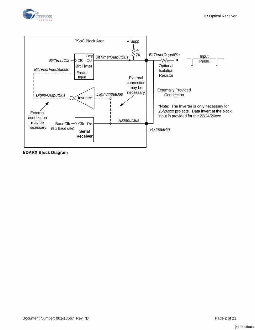
IrDARX Block Diagram
BaudClk(8 x Baud rate)
BitTimerClk
V Supp.
4.7K Input
Pulse
Clk Rx
SerialReceiver
ClkCmpOut
EnableInput
Bit Timer Optional Isolation Resistor
PSoC Block Area
Inverter*
RXInputBus
RXInputPin
BitTimerOutputBus
Externally Provided Connection
BitTimerOuputPin
External connection
may be necessary
BitTimerFeedBackIn
DigInvOutputBus DigInvInputBus
External connection
may be necessary
*Note: The Inverter is only necessary for 25/26xxx projects. Data invert at the block input is provided for the 22/24/26xxx
[+] Feedback

IR Optical Receiver
Document Number: 001-13567 Rev. *D Page 3 of 21
Functional Description IrDARX is a user module that implements the hardware detection and timing requirements to receive IrDA-compliant infrared data from a suitable optical detector. The IrDARX User Module uses 2 PsoC blocks, one of which must be a Communication Type block. A companion user module, IrDATX, provides a similarly implemented infrared transmitter. Since IrDA is inherently a half-duplex protocol, these two user modules can be placed in the same locations, using dynamic re-configuration with minimal consumption of device resources.The IrDARX and IrDATX User Modules operate independently. Due to problems with optical reflections and cross talk, the IrDA receiver and transmitter do not operate at the same time in conventional applications.In simplified terms, at the hardware physical interface level, IrDA optimizes standard serial communication for transmission over a wireless optical interface. An RS-232-compliant serial signal consists of an electrical signal idling at a non-zero (logic 1) voltage and data bits of a predefined duration framed by a start (logic 0), parity bit, and stop (logic 1) bit. To aid in detection of correct logic levels, voltages are held stable for the entire duration of a bit period and are detected by measuring voltage during the middle of the bit period.IrDA, on the other hand, is typically transmitted through an optical environment that is extremely noisy. Rather than measure light levels, which are variable with distance, angle, and transmitted power level, the IrDA hardware interface relies on brief duration, high-intensity optical pulses to set timing for transmitted bits. Pulses are only transmitted on data values of logic 0 (which takes care of the start bit and all 0 bits in a transmitted byte). The stop bit, logic 1 – no optical pulse, acts as a quiet bit, setting a minimum delay before the next start bit. This is shown in the following figure.
IrDA versus RS-232 Data Comparison
The IrDA specification allows data pulses between 1.67 microsecond and a maximum of 3/16 of one bit width at the operating baud rate. That is, there is a firm minimum pulse width but a variable maximum pulse width. An evaluation of the expected incoming pulse width is required to properly set up the IrDARX User Module.The IrDARX User Module operates by converting IrDA pulses into an RS-232-compliant waveform. To accomplish this, a PSoC digital block is configured as a counter, BitTimer, configured to form a re-triggerable one-shot. For CY8C27/24/22xxx designs, consideration of the various invert options is critical. The output of the BitTimer is routed to an output pin and must pass through the output LUT where a configurable invert is available, as the circuit is described here, an invert at the LUT should not be used. Every DigBlock input is automatically provided with an optional invert. Once the BitTimer output and input signal have been logically added the combination of the two signals must be inverted.
A: RS-232 Serial Data
Start Bit
Stop Bit
B: IrDA Serial Data0 1 1 0 0 1 0 0 0 1
[+] Feedback
IR Optical Receiver
Document Number: 001-13567 Rev. *D Page 4 of 21
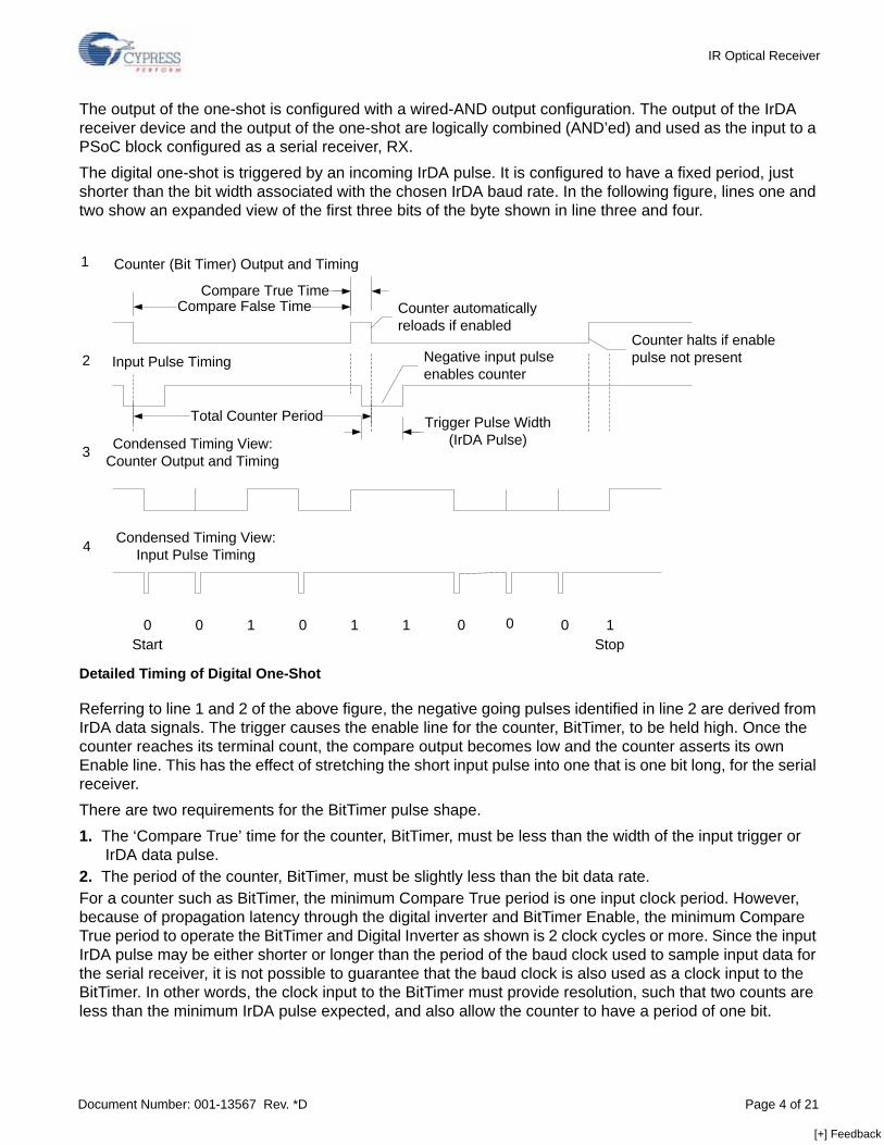
The output of the one-shot is configured with a wired-AND output configuration. The output of the IrDA receiver device and the output of the one-shot are logically combined (AND’ed) and used as the input to a PSoC block configured as a serial receiver, RX.The digital one-shot is triggered by an incoming IrDA pulse. It is configured to have a fixed period, just shorter than the bit width associated with the chosen IrDA baud rate. In the following figure, lines one and two show an expanded view of the first three bits of the byte shown in line three and four.
Detailed Timing of Digital One-Shot
Referring to line 1 and 2 of the above figure, the negative going pulses identified in line 2 are derived from IrDA data signals. The trigger causes the enable line for the counter, BitTimer, to be held high. Once the counter reaches its terminal count, the compare output becomes low and the counter asserts its own Enable line. This has the effect of stretching the short input pulse into one that is one bit long, for the serial receiver. There are two requirements for the BitTimer pulse shape.1. The ‘Compare True’ time for the counter, BitTimer, must be less than the width of the input trigger or
IrDA data pulse.2. The period of the counter, BitTimer, must be slightly less than the bit data rate.For a counter such as BitTimer, the minimum Compare True period is one input clock period. However, because of propagation latency through the digital inverter and BitTimer Enable, the minimum Compare True period to operate the BitTimer and Digital Inverter as shown is 2 clock cycles or more. Since the input IrDA pulse may be either shorter or longer than the period of the baud clock used to sample input data for the serial receiver, it is not possible to guarantee that the baud clock is also used as a clock input to the BitTimer. In other words, the clock input to the BitTimer must provide resolution, such that two counts are less than the minimum IrDA pulse expected, and also allow the counter to have a period of one bit.
Counter (Bit Timer) Output and Timing
Input Pulse Timing
Condensed Timing View:Counter Output and Timing
Condensed Timing View:Input Pulse Timing
Compare True Time
Total Counter Period Trigger Pulse Width(IrDA Pulse)
Compare False Time Counter automatically reloads if enabled
Negative input pulse enables counter
Counter halts if enable pulse not present
1
2
3
4
0 0 1 0 1 1 0 0 0Start
1Stop
[+] Feedback
IR Optical Receiver
Document Number: 001-13567 Rev. *D Page 5 of 21
DC and AC Electrical Characteristics
Parameters and Resources Each of the following parameters corresponds to a user configurable selection in PSoC designer. Parameters corresponding to global buses or input/output pins are in italic font in the block diagram. To view the block diagram from the PSoC Designer user interface, select View >> Config >> Windows, and then the user module block diagram.
BaudClkIrDARX is clocked by one of 16 possible sources. The Global I/O busses may be used to connect the clock input to an external pin or a clock function generated by a different PSoC block. The 48 MHz clock, the CPU_32 kHz clock, one of the divided clocks, 24V1 or 24V2, or another PSoC block output can be specified as the clock input. The clock rate must be set to eight times the desired bit rate. One data bit is received or transmitted every eight clocks cycles.
RX Input BusUsing a global bus, the input can be connected to one of the external pins. This input should be configured to provide Bit-Stretched data form the Digital One-Shot. This can be done using an internal or external (pin-tied-to-pin) connection, depending on block placement. Alternately, the input of the receiver can be connected to a low, high, neighboring PSoC block, or the analog comparator output bus.
Invert RX Input BusThis parameter is automatically added as a user parameter. Under most circumstances, this parameter should be set to ‘Normal’.
BitTimerClkThe clock is selected from one of 16 sources. These sources include the 48 MHz oscillator (5.0V operation only), lower frequencies (24V1 and 24V2) divided down from the 24 MHz system clock, other PSoC blocks, and external inputs routed through global inputs and outputs. If the BitTimerAutoSet parameter is selected, then this clock must conform to the specification indicated for each selection in the pull down parameter menu. (Reference the following parameter.)
BitTimerAutoSetThis parameter sets the period and compare value of the BitTimer counter. When given baud rates (bits/second) are configured using this parameter, a fixed set of Period/Compare values are loaded into the BitTimer counter. The user is required to provide a clock of the value indicated in the parameter. The values indicated are also suitable for use as input to a counter used to provide the BaudClk to the Transmit block (TX). Using the values suggested here, allow a single clock source to be provided to both to the
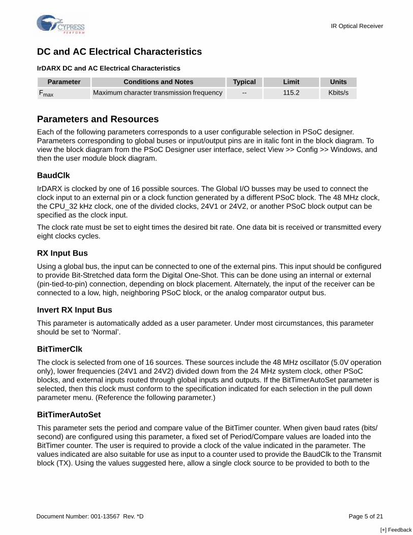
IrDARX DC and AC Electrical Characteristics
Parameter Conditions and Notes Typical Limit UnitsFmax Maximum character transmission frequency -- 115.2 Kbits/s
[+] Feedback

IR Optical Receiver
Document Number: 001-13567 Rev. *D Page 6 of 21
BitTimer and to a separate 8-bit counter (external to this user module), to provide a BaudClk to the Serial Receiver (RX) block.
BitTimer OutputThe output must be routed to one of the four possible global output signals. When operational as an IrDA receiver, the global output of this block must be routed to a pin configured with a pull-up output drive and externally routed to the input of the Digital Inverter (DigInv). The connection of this pin, to the input pin of the Digital Inverter, forms a summing junction for IrDA digital input.
BitTimerFeedbackIn (Enable)This parameter must be configured to a value identical to that of the ‘BitTimerFeedBackOut’ parameter of the Digital Inverter Block (DigInv). Together the BitTimer and the DigInv blocks form a digital one-shot with a programmable period and duty cycle. If the BitTimer and Digital Inverter blocks are placed such that no internal connection is possible, then a suitable PC board connection to pins must be made manually, using the Interconnect View. (Click Menu and select Config >> Pinout.)
InvertBitTimerFeedbackInThis Parameter should be set to ‘Invert’ to provide the negative feedback necessary for proper operation of the digital one-shot at the heart of the IrDARX block. (See the Functional Description).
RX and BitTimer ClockSyncIn the PSoC devices, digital blocks may provide clock sources in addition to the system clocks. Digital clock sources may even be chained in ripple fashion. This introduces skew with respect to the system clocks. These skews are more critical in the CY8C29/27/24/22/21xxx PSoC device families because of various data-path optimizations, particularly those applied to the system busses. These parameter which specify the synchronization clock for each of the RX and the BitTimer blocks may be used to control clock skew and ensure proper operation when reading and writing PSoC block register values. Appropriate values for these parameters should be determined from the following table.
CAUTION The Period, Compare Value, and Compare Type must be set to values that provide a pulse of duty cycle and period, to allow proper operation of the user module. (Refer to the Func-tion Description for additional information.)
ClockSync Value UseSync to SysClk Use this setting for any 24 MHz (SysClk) derived clock source that is divided by two or more.
Examples include VC1, VC2, VC3 (when VC3 is driven by SysClk), 32KHz, and digital PSoC blocks with SysClk-based sources. Externally generated clock sources should also use this value to ensure that proper synchronization occurs.
Sync to SysClk*2 Use this setting for any 48 MHz (SysClk*2) based clock unless the resulting frequency is 48 MHz (in other words, when the product of all divisors is 1).
Use SysClk Direct Use when a 24 MHz (SysClk/1) clock is desired. This does not actually perform synchroniza-tion but provides low-skew access to the system clock itself. If selected, this option overrides the setting of the Clock parameter, above. It should always be used instead of VC1, VC2, VC3 or Digital Blocks where the net result of all dividers in combination produces a 24 Mhz output.
Unsynchronized Use when the 48 MHz (SysClk*2) input is selected.Use when unsynchronized inputs are desired. In general this use is advisable only when interrupt generation is the sole application of the Counter.
[+] Feedback

IR Optical Receiver
Document Number: 001-13567 Rev. *D Page 7 of 21
Interrupt Generation ControlThe following two parameters InterruptAPI and IntDispatchMode are only accessible by setting the Enable Interrupt Generation Control check box in PSoC Designer. This is available under Project >> Settings... >> Device Editor.
InterruptAPIThe InterruptAPI parameter allows conditional generation of a User Module’s interrupt handler and interrupt vector table entry. Select “Enable” to generate the interrupt handler and interrupt vector table entry. Select “Disable” to bypass the generation of the interrupt handler and interrupt vector table entry. Properly selecting whether an Interrupt API is to be generated is recommended particularly with projects that have multiple overlays where a single block resource is used by the different overlays. By selecting only Interrupt API generation when it is necessary the need to generate an interrupt dispatch code might be eliminated, thereby reducing overhead.
IntDispatchModeThe IntDispatchMode parameter is used to specify how an interrupt request is handled for interrupts shared by multiple user modules existing in the same block but in different overlays. Selecting “ActiveStatus” causes firmware to test which overlay is active before servicing the shared interrupt request. This test occurs every time the shared interrupt is requested. This adds latency and also produces a nondeterministic procedure of servicing shared interrupt requests, but does not require any RAM. Selecting “OffsetPreCalc” causes firmware to calculate the source of a shared interrupt request only when an overlay is initially loaded. This calculation decreases interrupt latency and produces a deterministic procedure for servicing shared interrupt requests, but at the expense of a byte of RAM.
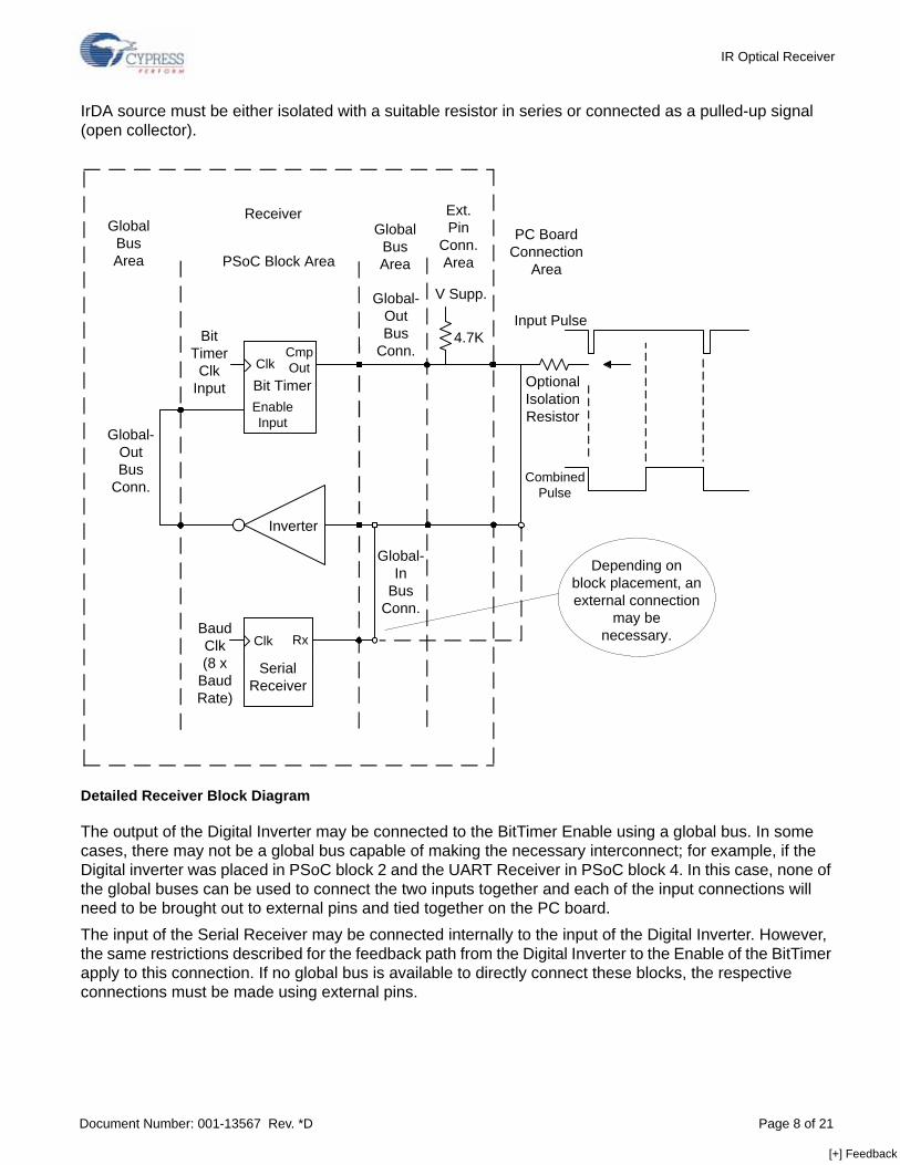
Placement The IrDARX User Module may be placed in three digital blocks. The Serial Receiver must be placed in a Digital Communication Type A block. If standard digital blocks (DBA00 – DBA03) are used, one or more external pin connections are required for block interconnects.Connection of the three blocks and input signals for the IrDARX User Module require that there be a logical AND of the input signal and the output of the BitTimer. Since no combinational logic between PSoC blocks is provided, a wired-AND logic configuration is used. This requires that the output of the BitTimer be connected to an external pin configured with an internal pull-up resistor. The data connection from the
[+] Feedback
IR Optical Receiver
Document Number: 001-13567 Rev. *D Page 8 of 21
IrDA source must be either isolated with a suitable resistor in series or connected as a pulled-up signal (open collector).
Detailed Receiver Block Diagram
The output of the Digital Inverter may be connected to the BitTimer Enable using a global bus. In some cases, there may not be a global bus capable of making the necessary interconnect; for example, if the Digital inverter was placed in PSoC block 2 and the UART Receiver in PSoC block 4. In this case, none of the global buses can be used to connect the two inputs together and each of the input connections will need to be brought out to external pins and tied together on the PC board. The input of the Serial Receiver may be connected internally to the input of the Digital Inverter. However, the same restrictions described for the feedback path from the Digital Inverter to the Enable of the BitTimer apply to this connection. If no global bus is available to directly connect these blocks, the respective connections must be made using external pins.
Baud Clk(8 x
Baud Rate)
Bit Timer
Clk Input
Global-OutBus
Conn.
Global-In
Bus Conn.
Global-OutBus
Conn.
V Supp.
4.7K
Global Bus Area
Global BusArea
Ext.Pin
Conn.Area
PC BoardConnection
Area
Receiver
CombinedPulse
RxClk
SerialReceiver
Inverter
ClkCmpOut
EnableInput
Bit Timer
Input Pulse
PSoC Block Area
Optional Isolation Resistor
Depending onblock placement, an external connection
may be necessary.
[+] Feedback

IR Optical Receiver
Document Number: 001-13567 Rev. *D Page 9 of 21
Receive Block – RX OperationThe receiver uses the RX Buffer, RX Shift, and RX Control registers of a Digital Communications Type PSoC block. The RX Control register is initialized and configured, using the IrDARX User Module firmware API routines. Initialization of the RX block consists of setting the Serial Receiver input bus and pin, and optionally enabling the interrupt on the Rx Register Full condition. The Serial Receiver User Module clock must be configured at eight times the baud rate desired, as described for the RX8 User Module. The clock is configured using the PSoC Designer Device Editor.The data received and transmitted is a bit stream that consists of a start bit, eight data bits, and a stop bit.When a start bit is detected on the RX input, a divide-by-eight bit clock is started and synchronized to sample the data in the center of received bits. On the rising edge of the next eight-bit clocks, the input data is sampled and shifted into the RX Shift register. The sampling of the stop bit on the next clock results in the received data byte transfer to the RX Buffer register and the triggering of one or more of the following events:
• Rx Register Full bit in the RX Control register is set, and if the interrupt for the RX is enabled, then the associated interrupt is triggered.
• If the stop bit is not detected at the expected bit position in the data stream, then the Framing Error bit in the RX Control register is set.
• If the Buffer register has not been read before the stop bit of the currently received data, then the Over-run Error bit in the RX Control register is set.
For polling detection of a completely received data byte, the Rx Register Full bit in the RX Control register should be monitored. Data must be read out of the RX Buffer register before the next byte is completely received, to prevent the overrun error condition.
Pin ConfigurationThe IrDARX User Module will work well when configured as a loadable configuration. Care should be taken to set pin drive settings in other loadable configurations, so that external devices are driven (or not driven) when the IrDARX module is not in use. Although certain pins are set with specific drive settings when the IrDARX module is loaded, the pin settings will be set to their ‘base’ configuration when the IrDARX module is Unloaded.Because this user module uses pull-down pin drive settings, care should be taken when using ‘read-modify-write’ commands on the ports where these pins are defined. Ideally, a shadow register should be used to alter data settings on the port.For example, you may wish to avoid changing bit-0 of portX. If the pin is configured as a pull up or pull down but an external source is driving it to a different state than the output register, the external data may be read and then re-written to the port, resulting in un-intended alteration of the output data.Condition:
PRTXDR is configured with bit 0 driven with a pull up. Data in the Data register is set to bit-0=1. An external source is pulling the output of bit 1 low. When the port is read, a zero will be read at bit-0, rather than the one in the Data register. A read-modify-write operation on the Data register will then read the zero in bit 0 and write it back to the Data register.
In C:BYTE portXShadow;//make sure that any changes to PRTXDR are recorded in portXShadowportXShadow = 0x80 | portXShadow;PRTXDR = portXShadow;
[+] Feedback
IR Optical Receiver
Document Number: 001-13567 Rev. *D Page 10 of 21
In Assembly:portXShadow: blk 1;make sure any changes to PRTXDR are recorded in portXShadowor [portXShadow], 0x80mov A, [portXShadow]mov reg[PRTXDR], A
Application Programming Interface The Application Programming Interface (API) routines are provided as part of the user module to allow the designer to deal with the module at a higher level. This section specifies the interface to each function together with related constants provided by the “include” files.Note In this, as in all user module APIs, the values of the A and X register may be altered by calling an
API function. It is the responsibility of the calling function to preserve the values of A and X prior to the call if those values are required after the call. This “registers are volatile” policy was selected for efficiency reasons and has been in force since version 1.0 of PSoC Designer. The C compiler automatically takes care of this requirement. Assembly language programmers must ensure their code observes the policy, too. Though some user module API function may leave A and X unchanged, there is no guarantee they will do so in the future.
The Application Programming Interface routines will allow programmatic control of the IrDARX User Module.
IrDARX_StartDescription:
Enables the Serial Receiver, the BitTimer, and the DigInv blocks. Once enabled, data can be received. C Prototype:
void IrDARX__Start(void)
Assembly:call IrDARX__Start
ParametersNone
Return Value: None
Side Effects: The A and X registers may be modified by this or future implementations of this function. The same is true for all RAM page pointer registers in the Large Memory Model (CY8C29xxx). When necessary, it is the calling function's responsibility to preserve the values across calls to fastcall16 functions.
IrDARX_Stop Description:
Disables the IrDARX User Module by disabling each functional block involved, the Serial Receiver, Bit-Timer, and the DigInv.
C Prototype:void IrDARX__Stop(void)
Assembly:call IrDARX__Stop
[+] Feedback
IR Optical Receiver
Document Number: 001-13567 Rev. *D Page 11 of 21
ParametersNone
Return Value: None
Side Effects: The A and X registers may be modified by this or future implementations of this function. The same is true for all RAM page pointer registers in the Large Memory Model (CY8C29xxx). When necessary, it is the calling function's responsibility to preserve the values across calls to fastcall16 functions.
IrDARX_EnableIntDescription:
Selects and enables both UART interrupt(s), by setting the appropriate interrupt enable bits.C Prototype:
void IrDARX__EnableInt(void)
Assembly:call IrDARX__EnableInt
ParametersNone
Return Value: None
Side Effects: If an interrupt is pending and this API is called, an interrupt will be triggered immediately. This call should be made prior to calling Start(). The A and X registers may be modified by this or future imple-mentations of this function. The same is true for all RAM page pointer registers in the Large Memory Model (CY8C29xxx). When necessary, it is the calling function's responsibility to preserve the values across calls to fastcall16 functions.
IrDARX_DisableIntDescription:
Disables all UART interrupts. C Prototype:
void IrDARX__DisableInt(void)
Assembly:call IrDARX__DisableInt
ParametersNone
Return Value: None
Side Effects: The A and X registers may be modified by this or future implementations of this function. The same is true for all RAM page pointer registers in the Large Memory Model (CY8C29xxx). When necessary, it is the calling function's responsibility to preserve the values across calls to fastcall16 functions.
[+] Feedback
IR Optical Receiver
Document Number: 001-13567 Rev. *D Page 12 of 21
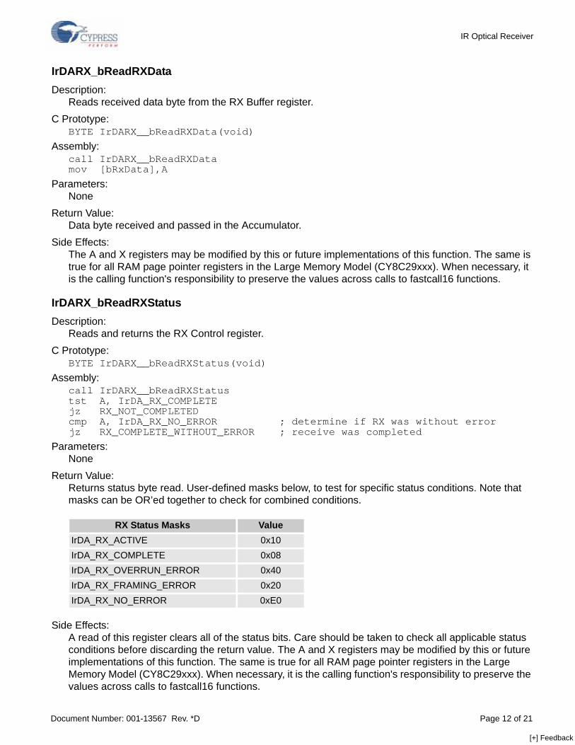
IrDARX_bReadRXDataDescription:
Reads received data byte from the RX Buffer register.C Prototype:
BYTE IrDARX__bReadRXData(void)
Assembly:call IrDARX__bReadRXDatamov [bRxData],A
Parameters: None
Return Value: Data byte received and passed in the Accumulator.
Side Effects: The A and X registers may be modified by this or future implementations of this function. The same is true for all RAM page pointer registers in the Large Memory Model (CY8C29xxx). When necessary, it is the calling function's responsibility to preserve the values across calls to fastcall16 functions.
IrDARX_bReadRXStatusDescription:
Reads and returns the RX Control register.C Prototype:
BYTE IrDARX__bReadRXStatus(void)
Assembly:call IrDARX__bReadRXStatustst A, IrDA_RX_COMPLETEjz RX_NOT_COMPLETEDcmp A, IrDA_RX_NO_ERROR ; determine if RX was without errorjz RX_COMPLETE_WITHOUT_ERROR ; receive was completed
Parameters: None
Return Value: Returns status byte read. User-defined masks below, to test for specific status conditions. Note that masks can be OR’ed together to check for combined conditions.
Side Effects: A read of this register clears all of the status bits. Care should be taken to check all applicable status conditions before discarding the return value. The A and X registers may be modified by this or future implementations of this function. The same is true for all RAM page pointer registers in the Large Memory Model (CY8C29xxx). When necessary, it is the calling function's responsibility to preserve the values across calls to fastcall16 functions.
RX Status Masks ValueIrDA_RX_ACTIVE 0x10IrDA_RX_COMPLETE 0x08IrDA_RX_OVERRUN_ERROR 0x40IrDA_RX_FRAMING_ERROR 0x20IrDA_RX_NO_ERROR 0xE0
[+] Feedback
IR Optical Receiver
Document Number: 001-13567 Rev. *D Page 13 of 21
IrDARX_BitTimerSetupDescription:
Sets up the BitTimer parameters to any valid set of values, assumes an 8-bit counter.C Prototype:
void IrDARX__BitTimerSetup(BYTE bPeriod, BYTE bCmpVal);
Assembly:call IrDARX__BitTimerSetup
Parameters: A: The Counter period, bPeriod
x: The Counter Compare Value, bCmpValReturn Value:
NoneSide Effects:
The A and X registers may be modified by this or future implementations of this function. The same is true for all RAM page pointer registers in the Large Memory Model (CY8C29xxx). When necessary, it is the calling function's responsibility to preserve the values across calls to fastcall16 functions.
[+] Feedback
IR Optical Receiver
Document Number: 001-13567 Rev. *D Page 14 of 21
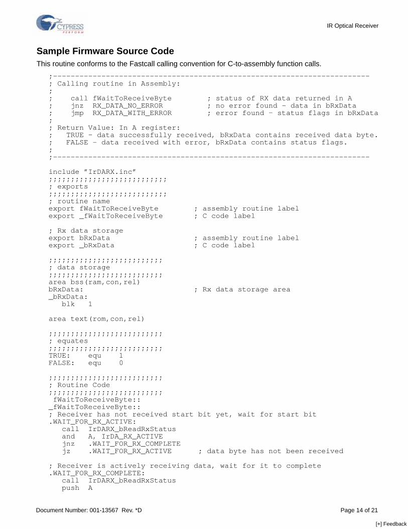
Sample Firmware Source Code This routine conforms to the Fastcall calling convention for C-to-assembly function calls.
;------------------------------------------------------------------------; Calling routine in Assembly:;; call fWaitToReceiveByte ; status of RX data returned in A; jnz RX_DATA_NO_ERROR ; no error found - data in bRxData ; jmp RX_DATA_WITH_ERROR ; error found - status flags in bRxData;; Return Value: In A register:; TRUE - data successfully received, bRxData contains received data byte.; FALSE - data received with error, bRxData contains status flags.;;------------------------------------------------------------------------
include ”IrDARX.inc”;;;;;;;;;;;;;;;;;;;;;;;;;;;; exports;;;;;;;;;;;;;;;;;;;;;;;;;;;; routine nameexport fWaitToReceiveByte ; assembly routine labelexport _fWaitToReceiveByte ; C code label
; Rx data storageexport bRxData ; assembly routine labelexport _bRxData ; C code label
;;;;;;;;;;;;;;;;;;;;;;;;;;; data storage;;;;;;;;;;;;;;;;;;;;;;;;;;area bss(ram,con,rel)bRxData: ; Rx data storage area_bRxData: blk 1
area text(rom,con,rel)
;;;;;;;;;;;;;;;;;;;;;;;;;;; equates;;;;;;;;;;;;;;;;;;;;;;;;;;TRUE: equ 1FALSE: equ 0
;;;;;;;;;;;;;;;;;;;;;;;;;;; Routine Code;;;;;;;;;;;;;;;;;;;;;;;;;; fWaitToReceiveByte::_fWaitToReceiveByte::; Receiver has not received start bit yet, wait for start bit.WAIT_FOR_RX_ACTIVE: call IrDARX_bReadRxStatus and A, IrDA_RX_ACTIVE jnz .WAIT_FOR_RX_COMPLETE jz .WAIT_FOR_RX_ACTIVE ; data byte has not been received
; Receiver is actively receiving data, wait for it to complete.WAIT_FOR_RX_COMPLETE: call IrDARX_bReadRxStatus push A
[+] Feedback

IR Optical Receiver
Document Number: 001-13567 Rev. *D Page 15 of 21
AND A, IrDA_RX_COMPLETE Jnz .CHECK_RX_ERRORS Pop A Jmp .WAIT_FOR_RX_COMPLETE
; Data completely received now check for errors.CHECK_RX_ERRORS: pop A call IrDARX_bReadRxStatus ; get the Rx status register and A, IrDA_RX_NO_ERROR ; mask off non-status bits jz .DATA_RX_WITH_NO_ERRORS ; data is valid - no error detected
; Errors detected in received data - return with error condition; 1) A is set to FALSE indicating error condition; 2) bRxData contains the RX status flags for further processing.RX_ERRORS_FOUND: mov [bRxData], A ; bRxData contains the status flags call IrDARX_bReadRxData ; Read RxData reg to prevent future ; overrun error mov A, FALSE ; Set A to FALSE condition ret
; No error detected in received data - return with data; 1) A is set to TRUE indicating NO error condition; 2) bRxData contains the received data byte.DATA_RX_WITH_NO_ERRORS: call IrDARX_bReadRxData ; get the received data in A mov [bRxData], A ; bRxData contains received data byte mov A, TRUE ; set a to NO error condition ret
END_fWaitToReceiveByte:
[+] Feedback

IR Optical Receiver
Document Number: 001-13567 Rev. *D Page 16 of 21
A sample project written in C follows.;------------------------------------------------------------------------;; Prototype:; BOOL fWaitToReceiveByte(void);;; Usage:; if ( fWaitToReceiveByte(); {; /* data valid - process it here! - data in bRxData */; };; Return Value: ; TRUE - data successfully received, bRxData contains received data byte.; FALSE - data received with error, bRxData contains status flags.;;------------------------------------------------------------------------
#include “IrDARX.h”#include “m8c.h”
/* Global bRxData */BYTE bRxData;
BOOL fWaitToReceiveByte(void){ BYTE bRxStatus;
/* wait for receiver to detect start bit */ while( !( IrDARX_bReadRxStatus() & IrDA_RX_ACTIVE ) ) { /* might want to sleep or keep track of time */ }
/* Start bit detected, wait to receive rest of data */ while ( !( bRxStatus = IrDARX_bReadRxStatus() & IrDA_RX_COMPLETE ) ) { /* might want to sleep or keep track of time */ }
/* data received, now check for errors */ if (( bRxStatus & IrDA_RX_NO_ERROR ) == 0 ) { /* no error detected */ bRxData = IrDARX_bReadRxData(); return( TRUE ); } else { /* error detected */ bRxData = bRxStatus; return( FALSE ); }}
[+] Feedback
IR Optical Receiver
Document Number: 001-13567 Rev. *D Page 17 of 21
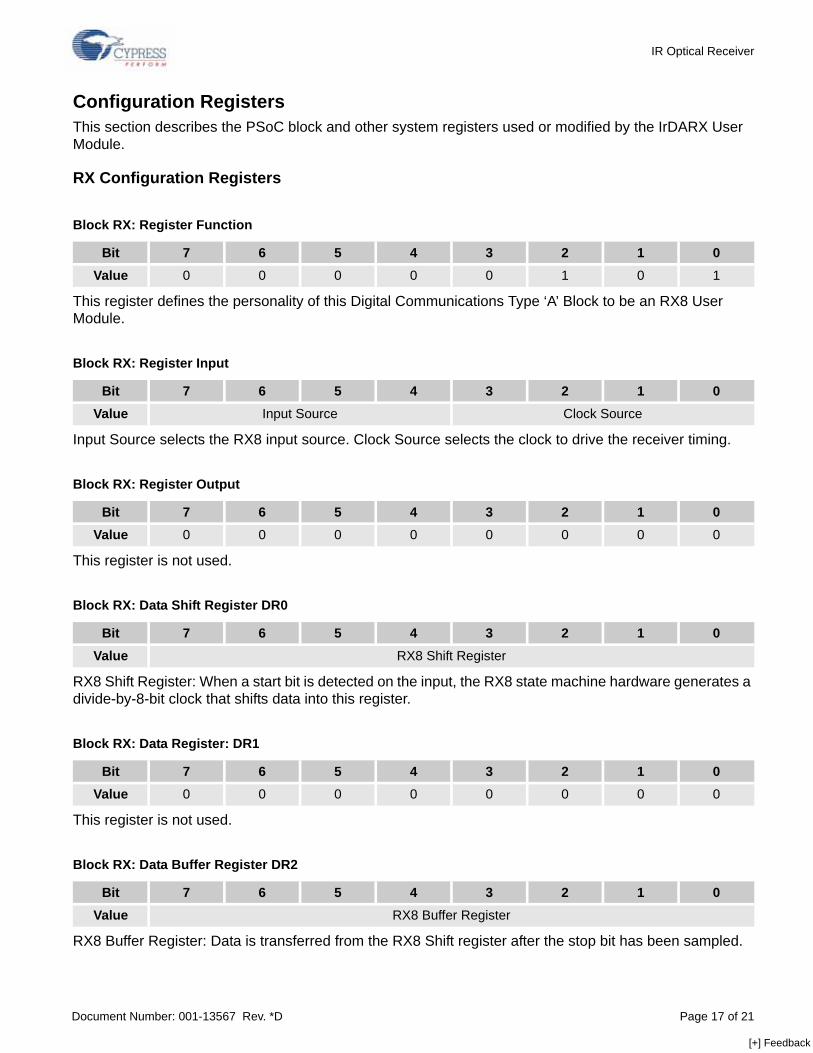
Configuration Registers This section describes the PSoC block and other system registers used or modified by the IrDARX User Module.
RX Configuration Registers
This register defines the personality of this Digital Communications Type ‘A’ Block to be an RX8 User Module.
Input Source selects the RX8 input source. Clock Source selects the clock to drive the receiver timing.
This register is not used.
RX8 Shift Register: When a start bit is detected on the input, the RX8 state machine hardware generates a divide-by-8-bit clock that shifts data into this register.
This register is not used.
RX8 Buffer Register: Data is transferred from the RX8 Shift register after the stop bit has been sampled.
Block RX: Register Function
Bit 7 6 5 4 3 2 1 0Value 0 0 0 0 0 1 0 1
Block RX: Register Input
Bit 7 6 5 4 3 2 1 0Value Input Source Clock Source
Block RX: Register Output
Bit 7 6 5 4 3 2 1 0Value 0 0 0 0 0 0 0 0
Block RX: Data Shift Register DR0
Bit 7 6 5 4 3 2 1 0Value RX8 Shift Register
Block RX: Data Register: DR1
Bit 7 6 5 4 3 2 1 0Value 0 0 0 0 0 0 0 0
Block RX: Data Buffer Register DR2
Bit 7 6 5 4 3 2 1 0Value RX8 Buffer Register
[+] Feedback
IR Optical Receiver
Document Number: 001-13567 Rev. *D Page 18 of 21
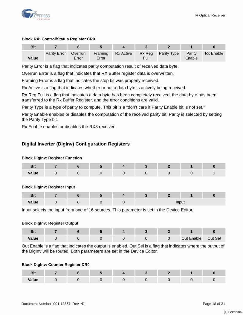
Parity Error is a flag that indicates parity computation result of received data byte.Overrun Error is a flag that indicates that RX Buffer register data is overwritten.Framing Error is a flag that indicates the stop bit was properly received.Rx Active is a flag that indicates whether or not a data byte is actively being received.Rx Reg Full is a flag that indicates a data byte has been completely received, the data byte has been transferred to the Rx Buffer Register, and the error conditions are valid.Parity Type is a type of parity to compute. This bit is a “don’t care if Parity Enable bit is not set.”Parity Enable enables or disables the computation of the received parity bit. Parity is selected by setting the Parity Type bit.Rx Enable enables or disables the RX8 receiver.
Digital Inverter (DigInv) Configuration Registers
Input selects the input from one of 16 sources. This parameter is set in the Device Editor.
Out Enable is a flag that indicates the output is enabled. Out Sel is a flag that indicates where the output of the DigInv will be routed. Both parameters are set in the Device Editor.
Block RX: Control/Status Register CR0
Bit 7 6 5 4 3 2 1 0
ValueParity Error Overrun
ErrorFraming
ErrorRx Active Rx Reg
FullParity Type Parity
EnableRx Enable
Block DigInv: Register Function
Bit 7 6 5 4 3 2 1 0Value 0 0 0 0 0 0 0 1
Block DigInv: Register Input
Bit 7 6 5 4 3 2 1 0Value 0 0 0 0 Input
Block DigInv: Register Output
Bit 7 6 5 4 3 2 1 0Value 0 0 0 0 0 0 Out Enable Out Sel
Block DigInv: Counter Register DR0
Bit 7 6 5 4 3 2 1 0Value 0 0 0 0 0 0 0 0
[+] Feedback
IR Optical Receiver
Document Number: 001-13567 Rev. *D Page 19 of 21
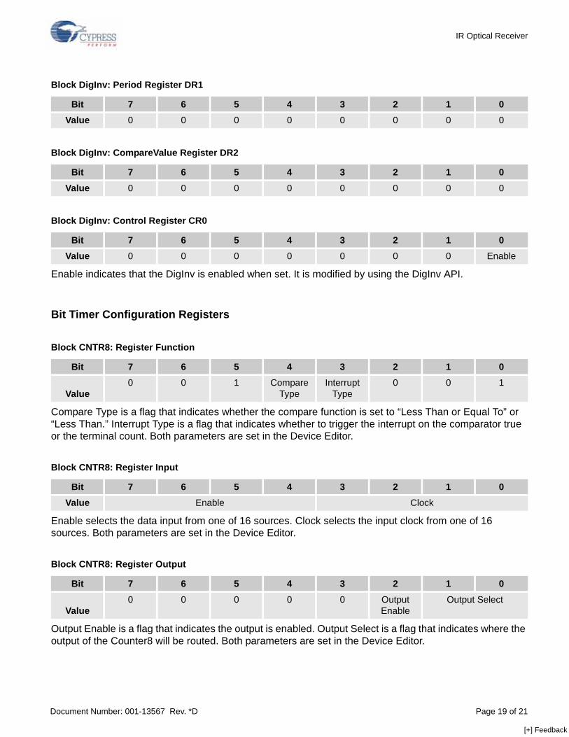
Enable indicates that the DigInv is enabled when set. It is modified by using the DigInv API.
Bit Timer Configuration Registers
Compare Type is a flag that indicates whether the compare function is set to “Less Than or Equal To” or “Less Than.” Interrupt Type is a flag that indicates whether to trigger the interrupt on the comparator true or the terminal count. Both parameters are set in the Device Editor.
Enable selects the data input from one of 16 sources. Clock selects the input clock from one of 16 sources. Both parameters are set in the Device Editor.
Output Enable is a flag that indicates the output is enabled. Output Select is a flag that indicates where the output of the Counter8 will be routed. Both parameters are set in the Device Editor.
Block DigInv: Period Register DR1
Bit 7 6 5 4 3 2 1 0Value 0 0 0 0 0 0 0 0
Block DigInv: CompareValue Register DR2
Bit 7 6 5 4 3 2 1 0Value 0 0 0 0 0 0 0 0
Block DigInv: Control Register CR0
Bit 7 6 5 4 3 2 1 0Value 0 0 0 0 0 0 0 Enable
Block CNTR8: Register Function
Bit 7 6 5 4 3 2 1 0
Value0 0 1 Compare
TypeInterrupt
Type0 0 1
Block CNTR8: Register Input
Bit 7 6 5 4 3 2 1 0Value Enable Clock
Block CNTR8: Register Output
Bit 7 6 5 4 3 2 1 0
Value0 0 0 0 0 Output
EnableOutput Select
[+] Feedback
IR Optical Receiver
Document Number: 001-13567 Rev. *D Page 20 of 21
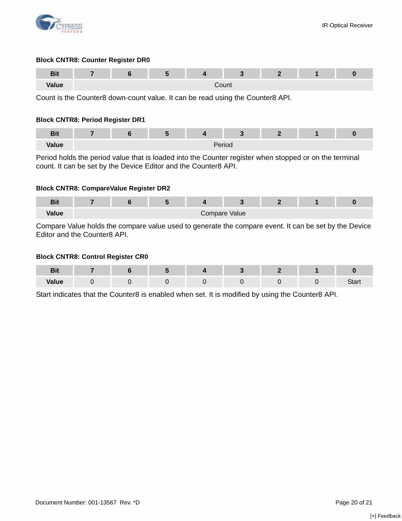
Count is the Counter8 down-count value. It can be read using the Counter8 API.
Period holds the period value that is loaded into the Counter register when stopped or on the terminal count. It can be set by the Device Editor and the Counter8 API.
Compare Value holds the compare value used to generate the compare event. It can be set by the Device Editor and the Counter8 API.
Start indicates that the Counter8 is enabled when set. It is modified by using the Counter8 API.
Block CNTR8: Counter Register DR0
Bit 7 6 5 4 3 2 1 0Value Count
Block CNTR8: Period Register DR1
Bit 7 6 5 4 3 2 1 0Value Period
Block CNTR8: CompareValue Register DR2
Bit 7 6 5 4 3 2 1 0Value Compare Value
Block CNTR8: Control Register CR0
Bit 7 6 5 4 3 2 1 0Value 0 0 0 0 0 0 0 Start
[+] Feedback

IR Optical Receiver
Document Number: 001-13567 Rev. *D Revised February 12, 2009 Page 21 of 21© Cypress Semiconductor Corporation, 2002-2009. The information contained herein is subject to change without notice. Cypress Semiconductor Corporation assumes no responsibility for theuse of any circuitry other than circuitry embodied in a Cypress product. Nor does it convey or imply any license under patent or other rights. Cypress products are not warranted nor intended to beused for medical, life support, life saving, critical control or safety applications, unless pursuant to an express written agreement with Cypress. Furthermore, Cypress does not authorize its productsfor use as critical components in life-support systems where a malfunction or failure may reasonably be expected to result in significant injury to the user. The inclusion of Cypress products in life-support systems application implies that the manufacturer assumes all risk of such use and in doing so indemnifies Cypress against all charges.
PSoC Designer™, Programmable System-on-Chip™, and PSoC Express™ are trademarks and PSoC® is a registered trademark of Cypress Semiconductor Corp. All other trademarks or registeredtrademarks referenced herein are property of the respective corporations.
Any Source Code (software and/or firmware) is owned by Cypress Semiconductor Corporation (Cypress) and is protected by and subject to worldwide patent protection (United States and foreign),United States copyright laws and international treaty provisions. Cypress hereby grants to licensee a personal, non-exclusive, non-transferable license to copy, use, modify, create derivative worksof, and compile the Cypress Source Code and derivative works for the sole purpose of creating custom software and or firmware in support of licensee product to be used only in conjunction witha Cypress integrated circuit as specified in the applicable agreement. Any reproduction, modification, translation, compilation, or representation of this Source Code except as specified above isprohibited without the express written permission of Cypress.
Disclaimer: CYPRESS MAKES NO WARRANTY OF ANY KIND, EXPRESS OR IMPLIED, WITH REGARD TO THIS MATERIAL, INCLUDING, BUT NOT LIMITED TO, THE IMPLIED WARRANTIESOF MERCHANTABILITY AND FITNESS FOR A PARTICULAR PURPOSE. Cypress reserves the right to make changes without further notice to the materials described herein. Cypress does notassume any liability arising out of the application or use of any product or circuit described herein. Cypress does not authorize its products for use as critical components in life-support systemswhere a malfunction or failure may reasonably be expected to result in significant injury to the user. The inclusion of Cypress' product in a life-support systems application implies that the manufacturerassumes all risk of such use and in doing so indemnifies Cypress against all charges.
Use may be limited by and subject to the applicable Cypress software license agreement.
[+] Feedback