15-213 caches march 16, 2000 - carnegie mellon school of ...caches march 16, 2000 15-213...
TRANSCRIPT

Topics• Memory Hierarchy• Locality of Reference• Cache Design
– Direct Mapped– Associative
CachesMarch 16, 2000
15-213
class18.ppt
CS 213 S’00– 2 –class18.ppt
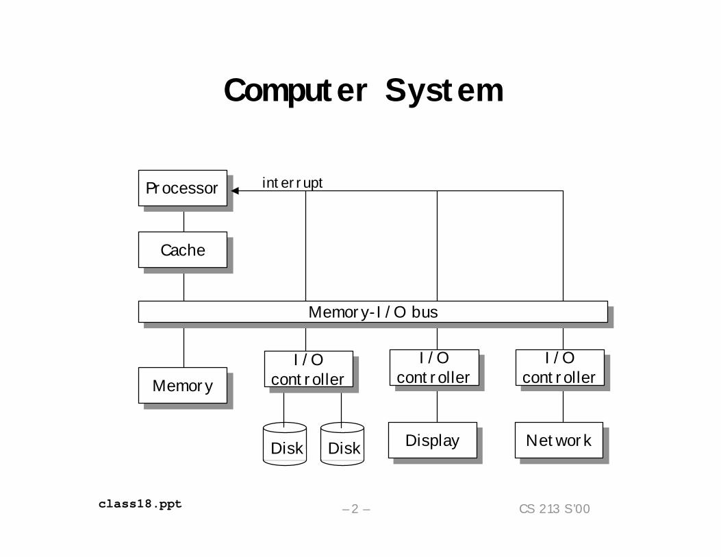
Computer System
diskDiskdiskDisk
Memory-I/O busMemory-I/O bus
ProcessorProcessor
CacheCache
MemoryMemoryI/O
controllerI/O
controllerI/Ocontroller
I/Ocontroller
I/Ocontroller
I/Ocontroller
DisplayDisplay NetworkNetwork
interrupt

CS 213 S’00– 3 –class18.ppt
Levels in Memory Hierarchy
CPUCPUregsregs
Cache
MemoryMemory diskdisk
size:speed:$/Mbyte:line size:
200 B2 ns
8 B
Register Cache Memory Disk Memory32KB - 4MB4 ns$100/MB32 B
128 MB60 ns$1.50/MB8 KB
20 GB8 ms$0.05/MB
larger, slower, cheaper
8 B 32 B 8 KB
cache virtual memory

CS 213 S’00– 4 –class18.ppt
Alpha 21164 Chip Photo
Microprocessor Report 9/12/94
Caches:L1 dataL1 instructionL2 unifiedTLBBranch history

CS 213 S’00– 5 –class18.ppt
Alpha 21164 Chip Caches
Caches:L1 dataL1 instructionL2 unifiedTLBBranch history
Right HalfL2
Right HalfL2
L1
Instr.
L1Data
L2Tags
L3 Control

CS 213 S’00– 6 –class18.ppt
Locality of ReferencePrinciple of Locality:
• Programs tend to reuse data and instructions near those they have used recently.
• Temporal locality: recently referenced items are likely to be referenced in the near future.
• Spatial locality: items with nearby addresses tend to be referenced close together in time.
sum = 0;for (i = 0; i < n; i++)
sum += a[i];*v = sum;Locality in Example:
• Data– Reference array elements in succession
(spatial)• Instructions
– Reference instructions in sequence (spatial)– Cycle through loop repeatedly (temporal)

CS 213 S’00– 7 –class18.ppt
Caching: The Basic IdeaMain Memory
• Stores wordsA–Z in example
Cache• Stores subset of the
words4 in example
• Organized in lines– Multiple words– To exploit spatial
localityAccess
• Word must be in cache for processor to access
Big, Slow Memory
ABC•••YZ
Small,Fast Cache
ABGH
Processor
CS 213 S’00– 8 –class18.ppt
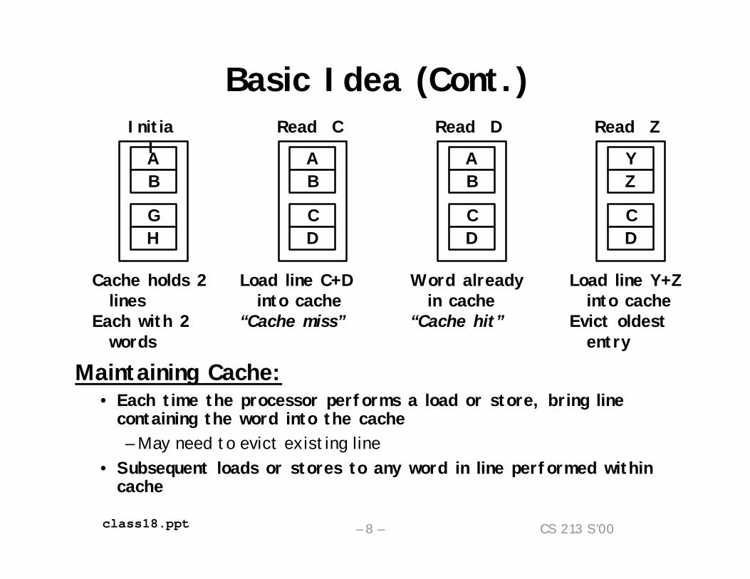
Basic Idea (Cont.)
Maintaining Cache:• Each time the processor performs a load or store, bring line
containing the word into the cache– May need to evict existing line
• Subsequent loads or stores to any word in line performed within cache
ABGH
Initial A
BCD
Read CABCD
YZCD
Read ZRead D
Cache holds 2 lines
Each with 2 words
Load line C+D into cache
“Cache miss”
Word already in cache
“Cache hit”
Load line Y+Z into cache
Evict oldest entry

CS 213 S’00– 9 –class18.ppt
• Between any two levels, memory is divided into lines (aka “blocks”)• Data moves between levels on demand, in line-sized chunks.• Invisible to application programmer
– Hardware responsible for cache operation• Upper-level lines a subset of lower-level lines.
a
ab
Access word w in line a (hit)
a
ab
Access word v in line b (miss)w
b
ab
ab
v
Accessing Data in Memory Hierarchy
HighLevel
LowLevel
CS 213 S’00– 10 –class18.ppt
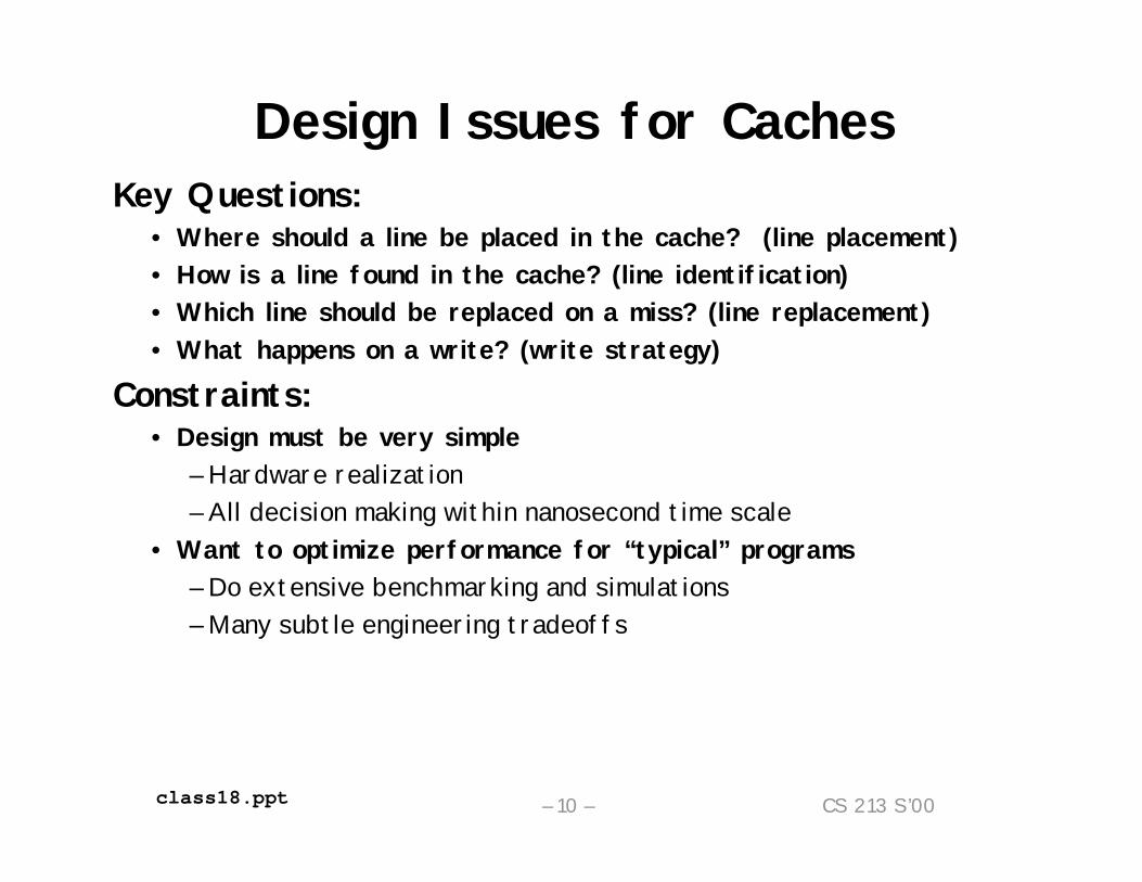
Design Issues for CachesKey Questions:
• Where should a line be placed in the cache? (line placement)• How is a line found in the cache? (line identification)• Which line should be replaced on a miss? (line replacement)• What happens on a write? (write strategy)
Constraints:• Design must be very simple
– Hardware realization– All decision making within nanosecond time scale
• Want to optimize performance for “typical” programs– Do extensive benchmarking and simulations– Many subtle engineering tradeoffs

CS 213 S’00– 11 –class18.ppt
Direct-Mapped CachesSimplest Design
• Each memory line has a unique cache locationParameters
• Line (aka block) size B = 2b
– Number of bytes in each line– Typically 2X–8X word size
• Number of Sets S = 2s
– Number of lines cache can hold• Total Cache Size = B*S = 2b+s
Physical Address• Address used to reference main memory• n bits to reference N = 2n total bytes• Partition into fields
– Offset: Lower b bits indicate which byte within line– Set: Next s bits indicate how to locate line within cache– Tag: Identifies this line when in cache
n-bit Physical Addresst s b
tag set index offset

CS 213 S’00– 12 –class18.ppt
Indexing into Direct-Mapped Cache
• Use set index bits to select cache set
Set 0: 0 1 • • • B–1Tag Valid
0 1 • • • B–1Tag Valid
0 1 • • • B–1Tag Valid
Set 1:
Set S–1:
•••
t s b
tag set index offsetPhysical Address

CS 213 S’00– 13 –class18.ppt
Direct-Mapped Cache Tag MatchingIdentifying Line
• Must have tag match high order bits of address
• Must have Valid = 10 1 • • • B–1Tag Valid
Selected Set:
t s b
tag set index offsetPhysical Address
= ?
= 1?
• Lower bits of address select byte or word within cache line

CS 213 S’00– 14 –class18.ppt
Direct Mapped Cache SimulationN=16 byte addresses, B=2 bytes/line, S=4 sets, E=1 entry/setAddress trace (reads):
0 [0000] 1 [0001] 13 [1101] 8 [1000] 0 [0000]0000000100100011010001010110011110001001101010111100110111101111
xt=1 s=2 b=1
xx x
1 0 m[1] m[0]v tag data
0 [0000] (miss)
(1)1 0 m[1] m[0]v tag data
1 1 m[13] m[12]
13 [1101] (miss)
(2)
1 1 m[9] m[8]v tag data
8 [1000] (miss)
(3)1 0 m[1] m[0]v tag data
1 1 m[13] m[12]
0 [0000] (miss)
(4)

CS 213 S’00– 15 –class18.ppt
Why Use Middle Bits as Index?
High-Order Bit Indexing• Adjacent memory lines would
map to same cache entry• Poor use of spatial locality
Middle-Order Bit Indexing• Consecutive memory lines map
to different cache lines• Can hold N-byte region of
address space in cache at one time
4-line Cache High-OrderBit Indexing
Middle-OrderBit Indexing
00011011
0000000100100011010001010110011110001001101010111100110111101111
0000000100100011010001010110011110001001101010111100110111101111

CS 213 S’00– 16 –class18.ppt
Direct Mapped Cache Implementation(DECStation 3100)tag set byte
offset
valid tag (16 bits) data (32 bits)
data
=
hit
16,384 sets
31 30 29 .................. 19 18 17 16 15 14 13 .................. 5 4 3 2 1 0

CS 213 S’00– 17 –class18.ppt
Properties of Direct Mapped CachesStrength
• Minimal control hardware overhead• Simple design• (Relatively) easy to make fast
Weakness• Vulnerable to thrashing• Two heavily used lines have same cache index• Repeatedly evict one to make room for other
Cache Line

CS 213 S’00– 18 –class18.ppt
Vector Product Example
Machine• DECStation 5000• MIPS Processor with 64KB direct-mapped cache, 16 B line size
Performance• Good case: 24 cycles / element• Bad case: 66 cycles / element
float dot_prod(float x[1024], y[1024]){float sum = 0.0;int i;for (i = 0; i < 1024; i++)sum += x[i]*y[i];
return sum;}

CS 213 S’00– 19 –class18.ppt
Thrashing Example
• Access one element from each array per iteration
x[1]x[0]
x[1020]
•••
•••
x[3]x[2]
x[1021]x[1022]x[1023]
y[1]y[0]
y[1020]
•••
•••
y[3]y[2]
y[1021]y[1022]y[1023]
CacheLine
CacheLine
CacheLine
CacheLine
CacheLine
CacheLine
CS 213 S’00– 20 –class18.ppt
x[1]x[0]
x[3]x[2]
y[1]y[0]
y[3]y[2]
CacheLine
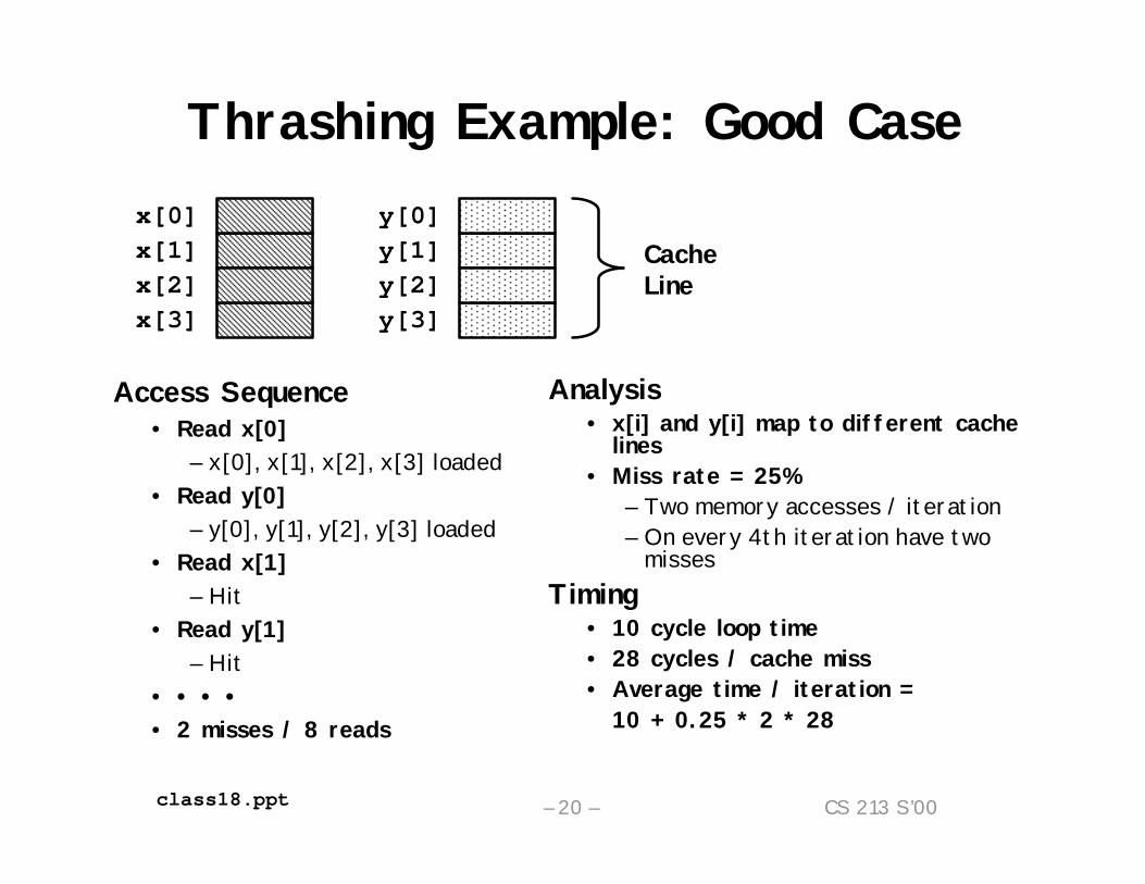
Thrashing Example: Good Case
Access Sequence• Read x[0]
– x[0], x[1], x[2], x[3] loaded• Read y[0]
– y[0], y[1], y[2], y[3] loaded• Read x[1]
– Hit• Read y[1]
– Hit• • • •• 2 misses / 8 reads
Analysis• x[i] and y[i] map to different cache
lines• Miss rate = 25%
– Two memory accesses / iteration– On every 4th iteration have two
missesTiming
• 10 cycle loop time• 28 cycles / cache miss• Average time / iteration =
10 + 0.25 * 2 * 28

CS 213 S’00– 21 –class18.ppt
x[1]x[0]
x[3]x[2]
y[1]y[0]
y[3]y[2]
CacheLine
Thrashing Example: Bad Case
Access Pattern• Read x[0]
– x[0], x[1], x[2], x[3] loaded• Read y[0]
– y[0], y[1], y[2], y[3] loaded• Read x[1]
– x[0], x[1], x[2], x[3] loaded• Read y[1]
– y[0], y[1], y[2], y[3] loaded• • •• 8 misses / 8 reads
Analysis• x[i] and y[i] map to same cache
lines• Miss rate = 100%
– Two memory accesses / iteration– On every iteration have two
missesTiming
• 10 cycle loop time• 28 cycles / cache miss• Average time / iteration =
10 + 1.0 * 2 * 28

CS 213 S’00– 22 –class18.ppt
Set Associative CacheMapping of Memory Lines
• Each set can hold E lines– Typically between 2 and 8
• Given memory line can map to any entry within its given setEviction Policy
• Which line gets kicked out when bring new line in• Commonly either “Least Recently Used” (LRU) or pseudo-random
– LRU: least-recently accessed (read or written) line gets evicted
Set i:0 1 • • • B–1Tag Valid
•••
0 1 • • • B–1Tag Valid
0 1 • • • B–1Tag Valid
LRU StateLine 0:Line 1:
Line E–1:

CS 213 S’00– 23 –class18.ppt
Set 0:
Set 1:
Set S–1:
•••
t s b
tag set index offsetPhysical Address
Indexing into 2-Way Associative Cache• Use middle s bits to
select from among S = 2ssets
0 1 • • • B–1Tag Valid0 1 • • • B–1Tag Valid0 1 • • • B–1Tag Valid0 1 • • • B–1Tag Valid
0 1 • • • B–1Tag Valid0 1 • • • B–1Tag Valid
CS 213 S’00– 24 –class18.ppt
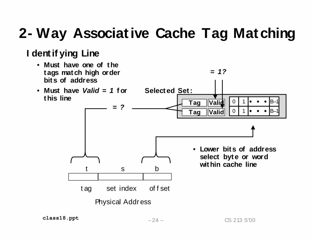
2-Way Associative Cache Tag MatchingIdentifying Line
• Must have one of the tags match high order bits of address
• Must have Valid = 1 for this line
Selected Set:
t s b
tag set index offsetPhysical Address
= ?
= 1?
• Lower bits of address select byte or word within cache line
0 1 • • • B–1Tag Valid0 1 • • • B–1Tag Valid
CS 213 S’00– 25 –class18.ppt
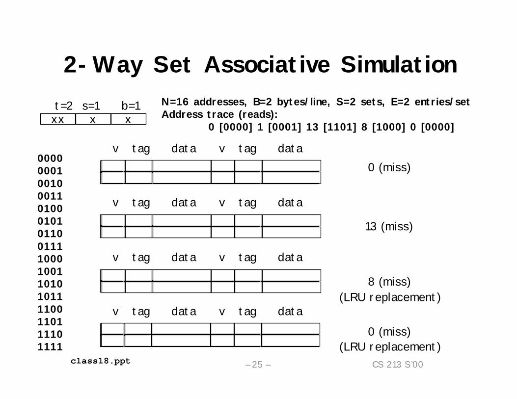
2-Way Set Associative SimulationN=16 addresses, B=2 bytes/line, S=2 sets, E=2 entries/setAddress trace (reads):
0 [0000] 1 [0001] 13 [1101] 8 [1000] 0 [0000]
0000000100100011010001010110011110001001101010111100110111101111
0 (miss)
13 (miss)
8 (miss)(LRU replacement)
0 (miss)(LRU replacement)
xxt=2 s=1 b=1
x x
1 00 m[1] m[0]
v tag data v tag data
v tag data v tag data1 00 m[1] m[0] 1 11 m[13] m[12]
1 10 m[9] m[8]
v tag data v tag data1 11 m[13] m[12]
1 10 m[9] m[8]
v tag data v tag data1 00 m[1] m[0]

CS 213 S’00– 26 –class18.ppt
Two-Way Set Associative CacheImplementation
• Set index selects a set from the cache• The two tags in the set are compared in parallel• Data is selected based on the tag result
Cache DataCache Line 0
Cache TagValid
:: :
Cache DataCache Line 0
Cache Tag Valid
: ::
Set Index
Mux 01Sel1 Sel0
Cache Line
CompareAdr Tag Compare
OR
Hit
Adr Tag

CS 213 S’00– 27 –class18.ppt
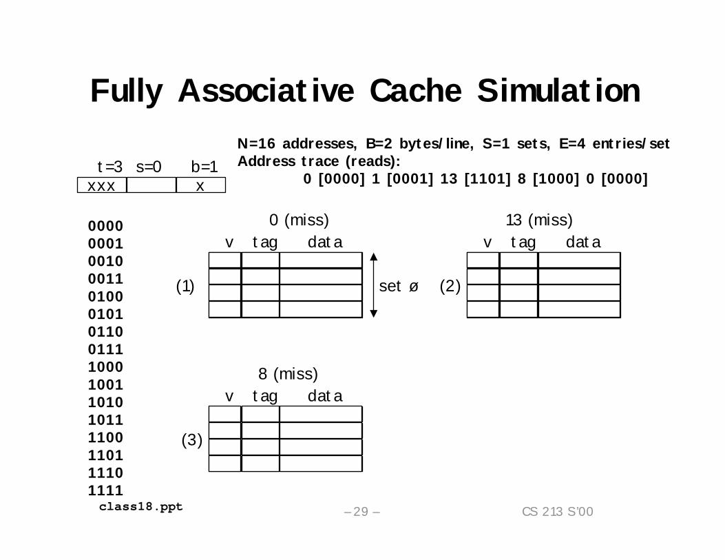
Fully Associative CacheMapping of Memory Lines
• Cache consists of single set holding E lines• Given memory line can map to any line in set• Only practical for small caches
Entire Cache
0 1 • • • B–1Tag Valid
•••
0 1 • • • B–1Tag Valid
0 1 • • • B–1Tag Valid
LRU StateLine 0:Line 1:
Line E–1:

CS 213 S’00– 28 –class18.ppt
Fully Associative Cache Tag MatchingIdentifying Line
• Must check all of the tags for match
• Must have Valid = 1 for this line
t b
tag offsetPhysical Address
= ?
= 1?
• Lower bits of address select byte or word within cache line
0 1 • • • B–1Tag Valid
•••
0 1 • • • B–1Tag Valid
0 1 • • • B–1Tag Valid
•••
CS 213 S’00– 29 –class18.ppt
Fully Associative Cache SimulationN=16 addresses, B=2 bytes/line, S=1 sets, E=4 entries/setAddress trace (reads):
0 [0000] 1 [0001] 13 [1101] 8 [1000] 0 [0000]
0000000100100011010001010110011110001001101010111100110111101111
xxxt=3 s=0 b=1
x
1 000 m[1] m[0]v tag data1 110 m[13] m[12]
13 (miss)
(2)
v tag data8 (miss)
(3)1 000 m[1] m[0]1 110 m[13] m[12]1 100 m[9] m[8]
1 00 m[1] m[0]v tag data
0 (miss)
(1) set ø

CS 213 S’00– 30 –class18.ppt
Write Policy• What happens when processor writes to the cache?• Should memory be updated as well?
Write Through:• Store by processor updates cache and memory.• Memory always consistent with cache• Never need to store from cache to memory• ~2X more loads than stores
ProcessorCache
MemoryStore
LoadCacheLoad

CS 213 S’00– 31 –class18.ppt
Write Strategies (Cont.)Write Back:
• Store by processor only updates cache line• Modified line written to memory only when it is evicted
– Requires “dirty bit” for each line» Set when line in cache is modified» Indicates that line in memory is stale
• Memory not always consistent with cache
ProcessorCache
MemoryStore
Load CacheLoad
WriteBack

CS 213 S’00– 32 –class18.ppt
Multi-Level Caches
size:speed:$/Mbyte:line size:
200 B2 ns
8 B
8-64 KB2 ns
32 B
128 MB DRAM60 ns$1.50/MB8 KB
9 GB8 ms$0.05/MB
larger, slower, cheaper
MemoryMemory diskdisk
TLB
L1 Icache
L1 Dcacheregs L2 Cache
Processor
1-4MB SRAM6 ns$100/MB32 B
larger line size, higher associativity, more likely to write back
Options: separate data and instruction caches, or a unified cache

CS 213 S’00– 33 –class18.ppt
Processor Chip
Alpha 21164 Hierarchy
• Improving memory performance was a main design goal• Earlier Alpha’s CPUs starved for data
L1 Data1 cycle latency
8KB, directWrite-throughDual Ported32B lines
L1 Instruction8KB, direct32B lines
Regs.L2 Unified
8 cycle latency96KB
3-way assoc.Write-back
Write allocate32B/64B lines
L3 Unified1M-64Mdirect
Write-backWrite allocate32B or 64B
lines
MainMemory
Up to 2GB
CS 213 S’00– 34 –class18.ppt
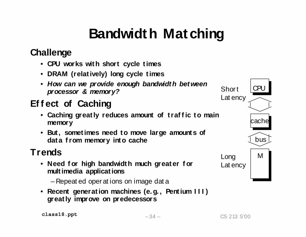
Bandwidth MatchingChallenge
• CPU works with short cycle times• DRAM (relatively) long cycle times• How can we provide enough bandwidth between
processor & memory?Effect of Caching
• Caching greatly reduces amount of traffic to main memory
• But, sometimes need to move large amounts of data from memory into cache
Trends• Need for high bandwidth much greater for
multimedia applications– Repeated operations on image data
• Recent generation machines (e.g., Pentium III) greatly improve on predecessors
CPU
cache
M
bus
ShortLatency
LongLatency
CS 213 S’00– 35 –class18.ppt
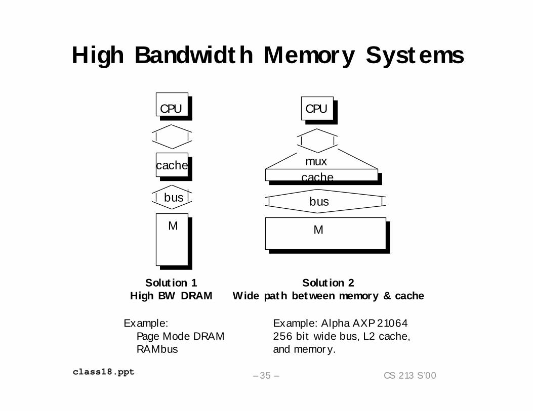
High Bandwidth Memory SystemsCPU
cache
M
bus
mux
CPU
cache
M
bus
Solution 1High BW DRAM
Solution 2Wide path between memory & cache
Example:Page Mode DRAMRAMbus
Example: Alpha AXP 21064256 bit wide bus, L2 cache, and memory.

CS 213 S’00– 36 –class18.ppt
Cache Performance MetricsMiss Rate
• fraction of memory references not found in cache (misses/references)
• Typical numbers:3-10% for L1can be quite small (e.g., < 1%) for L2, depending on size, etc.
Hit Time• time to deliver a line in the cache to the processor (includes time
to determine whether the line is in the cache)• Typical numbers:
1 clock cycle for L13-8 clock cycles for L2
Miss Penalty• additional time required because of a miss
– Typically 25-100 cycles for main memory