1.5 v stereo headphone preamplifier and power amplifier on typenumber/i-l/la4590.pdf · • stereo...
TRANSCRIPT
Ordering number : EN4468A
O3098HA (OT)/51894 (OT) A8-9763, 9024 No. 4468-1/19
LA4590W
SANYO Electric Co.,Ltd. Semiconductor Bussiness HeadquartersTOKYO OFFICE Tokyo Bldg., 1-10, 1 Chome, Ueno, Taito-ku, TOKYO, 110-8534 JAPAN
1.5 V Stereo Headphone Preamplifierand Power Amplifier
Monolithic Linear IC
Any and all SANYO products described or contained herein do not have specifications that can handleapplications that require extremely high levels of reliability, such as life-support systems, aircraft’scontrol systems, or other applications whose failure can be reasonably expected to result in seriousphysical and/or material damage. Consult with your SANYO representative nearest you before usingany SANYO products described or contained herein in such applications.
SANYO assumes no responsibility for equipment failures that result from using products at values thatexceed, even momentarily, rated values (such as maximum ratings, operating condition ranges, or otherparameters) listed in products specifications of any and all SANYO products described or containedherein.
OverviewThe LA4590W is a system IC that collects the functionsrequired for a playback set in a single chip, and reducesthe number of required external components. Furthermore,a recording system can be formed by combining theLA4590W with the LA3235W.
Functions• Stereo preamplifier (including functions for auto-
reverse, metal/normal tape switching, and muting)• Stereo power amplifier (including OCL and muting
functions)• Two ripple filters (single channel on/off switching)• Low boost (BTL operation at low frequencies)• AMS (inter-station detection function)• Power switch
Features• Preamplifier requires no NF capacitors.• Virtual ground impedance is reduced by built-in VREF
amplifier.• Ripple filter oscillation suppression requires no
capacitors.• Power output available when low boost is on.
(Po = 21 mW, VCC = 1.2 V, f = 100 Hz)• High cut capacitors built into preamplifier and power
amplifier. Buzz suppression• Miniature package: SQFP-48 (0.5 mm pitch)
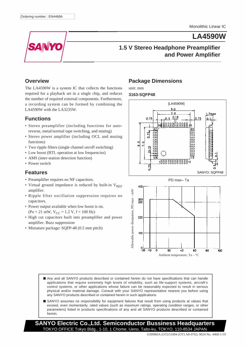
Package Dimensionsunit: mm
3163-SQFP48
PD max– Ta
Allo
wab
le p
ower
dis
sipa
tion,
PD
max
– m
W
Ambient temperature, Ta – °C
SANYO: SQFP48
[LA4590W]
Operating Characteristics at Ta = 25°C, VCC = 1.2 V, f = 1 kHz, 0.775 V = 0 dBm, RL = 10 kΩ (preamp), RL = 16 Ω (power amplifier)
Note: L.B.: Low boost
No. 4468-2/19
LA4590W
Parameter Symbol ConditionsRatings
Unitmin typ max
[Preamplifier + Power Amplifier]
Quiescent currentICCO1 Rg = 2.2 kΩ, RV = 0 Ω 8 15 24 mA
ICCO2 With the power switch off 0.1 5 µA
Voltage gain (closed) VGT VO = –20 dBm, RV = 10 kΩ 54 57 60 dB
[Preamplifier]
Voltage gain (open) VG0 VO = –20 dBm 60 67 dB
Voltage gain (closed)VG1 VO = –20 dBm 34 35.3 37 dB
VG2 VO = –20 dBm, f = 10 kHz, metal selected 25.5 28 30.5 dB
Maximum output voltage VO max THD = 1% 100 210 mV
Total harmonic distortion THD1 VG = 35.3 dB/NAB, VO = 100 mV 0.2 0.5 %
Input conversion noise voltage VNI Rg = 2.2 kΩ, BPF: 20 Hz to 20 kHz 1.3 3.0 µV
Crosstalk, inter-channel CT1 Rg = 2.2 kΩ, 1 kHz TUNE, VO = –20 dBm 45 56 dB
Crosstalk, F/R CT2 Rg = 2.2 kΩ, 1 kHz TUNE, VO = –20 dBm 65 78 dB
Ripple exclusion ratio Rr1Rg = 2.2 kΩ, Vr = –30 dBm, fr = 100 Hz
45 52 dB100 Hz TUNE
Muted output voltage VM1 Vi = –40 dBm, 1 kHz TUNE, Muting on –90 dBm
[Low boost + Power Amplifier]
VG3 VO = –20 dBm 20.5 23 25.5 dB
Voltage gain (closed)VG4 VO = –20 dBm, L.B. = on 20.5 23 25.5 dB
VG5 VO = –20 dBm, L.B. = on, f = 10 kHz 24.5 27.5 30.5 dB
VG6 VO = –20 dBm, L.B. = on, f = 100 Hz 30 34 38 dB
Output powerPO1 THD = 10% 5 9 mW
PO2 THD = 10%, f = 100 Hz, L.B. = on 13 21 mW
Total harmonic distortion THD2 PO = 1 mW 0.5 1.5 %
Inter-channel crosstalk CT3 VO = –20 dBm, RV = 0 Ω 38 43 dB
Output noise voltage VNO RV = 0 Ω, BPF: 20 Hz to 20 kHz 35 48 µV
Ripple exclusion ratio Rr2RV = 0 Ω, Vr = –30 dBm, fr = 100 Hz,
50 74 dB100 Hz TUNE
Muted output voltage VM2 Vi = –30 dBm, 1 kHz TUNE, Muting on –90 dBm
Input resistance Ri 8 10 12 kΩ
Voltage gain difference ∆VG3 0 1.5 dB
[Ripple Filter]
Ripple exclusion ratio Rr3fr = 100 Hz, Vr = –30 dBm, VCC = 1.0 V,
33 39 dBIRF = 25 mA, 2SB1295, using a rank 6 hFE
Output voltage VRF VCC = 1.0 V, IRF = 25 mA 0.89 0.93 V
[AMS]
Operating output voltage VOAMSWith the Preout output K22 on when the
1.80 2.55 3.6 mVAMS OUT output peak voltage is 0.6 Vp-p.
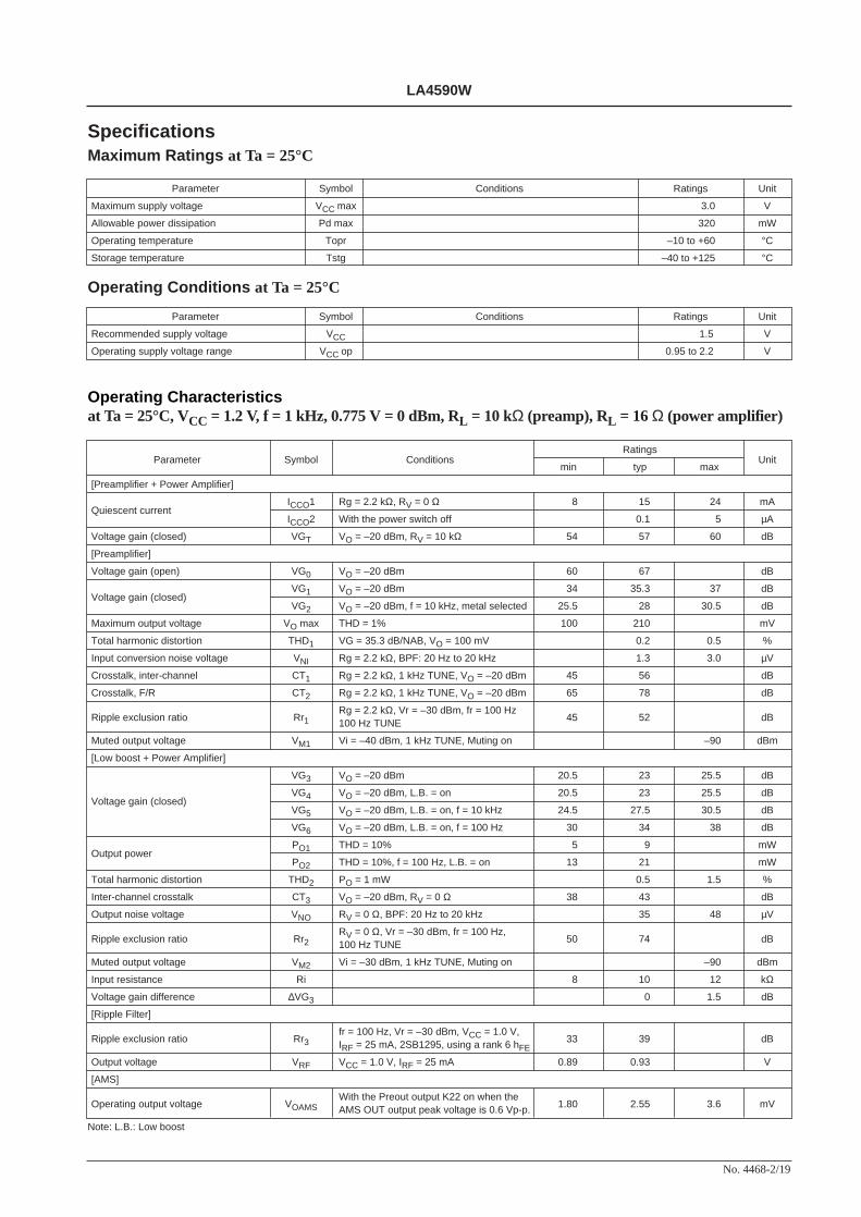
SpecificationsMaximum Ratings at Ta = 25°C
Operating Conditions at Ta = 25°C
Parameter Symbol Conditions Ratings Unit
Maximum supply voltage VCC max 3.0 V
Allowable power dissipation Pd max 320 mW
Operating temperature Topr –10 to +60 °C
Storage temperature Tstg –40 to +125 °C
Parameter Symbol Conditions Ratings Unit
Recommended supply voltage VCC 1.5 V
Operating supply voltage range VCC op 0.95 to 2.2 V
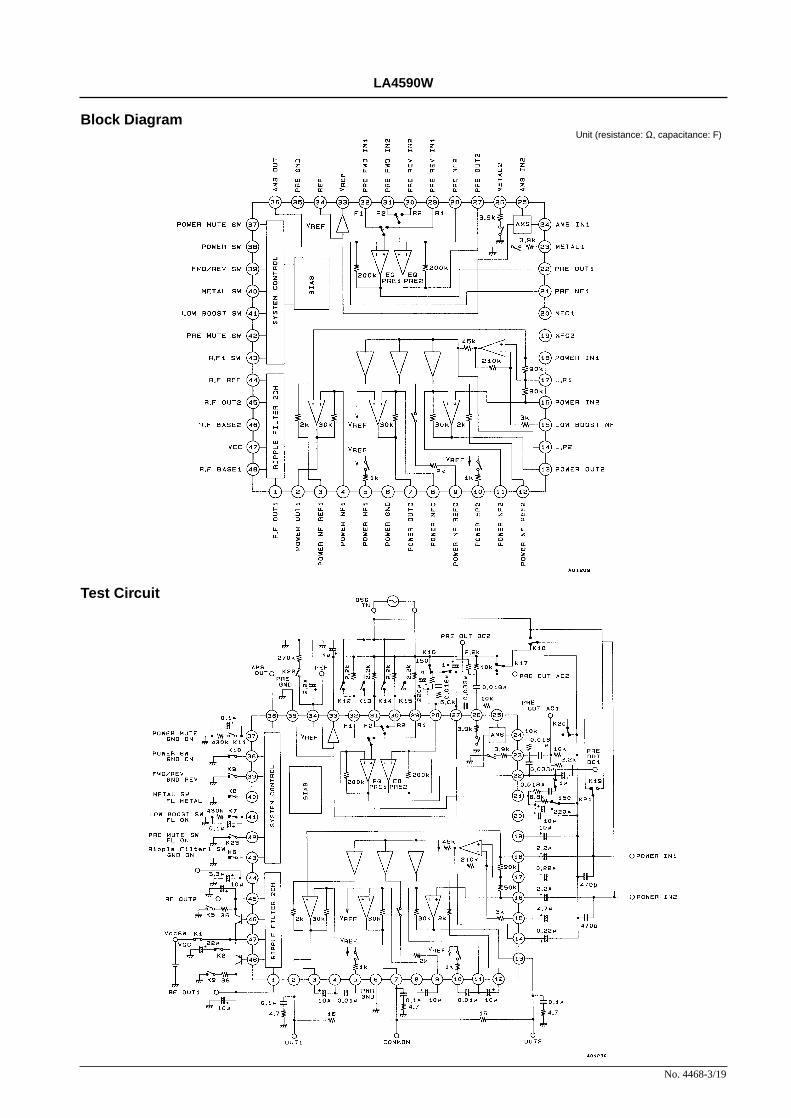
Block Diagram
Test Circuit
No. 4468-3/19
LA4590W
Unit (resistance: Ω, capacitance: F)
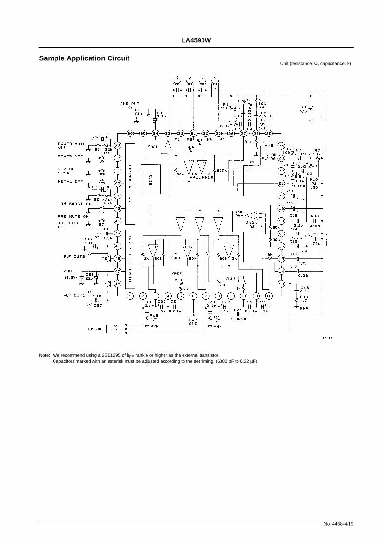
Sample Application Circuit
Note: We recommend using a 2SB1295 of hFE rank 6 or higher as the external transistor.Capacitors marked with an asterisk must be adjusted according to the set timing. (6800 pF to 0.22 µF)
No. 4468-4/19
LA4590W
Unit (resistance: Ω, capacitance: F)
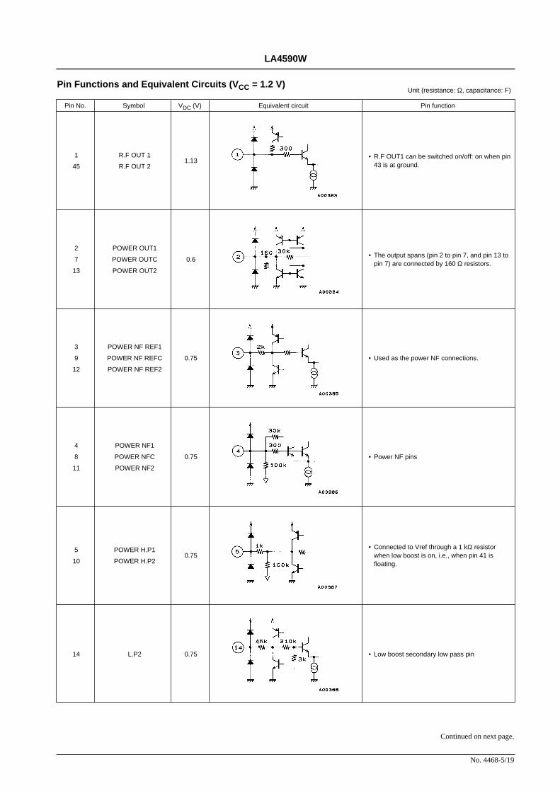
Pin Functions and Equivalent Circuits (VCC = 1.2 V)
No. 4468-5/19
LA4590W
Continued on next page.
Pin No. Symbol VDC (V) Equivalent circuit Pin function
1 R.F OUT 11.13
45 R.F OUT 2
2 POWER OUT1
7 POWER OUTC 0.6
13 POWER OUT2
3 POWER NF REF1
9 POWER NF REFC 0.75
12 POWER NF REF2
4 POWER NF1
8 POWER NFC 0.75
11 POWER NF2
5 POWER H.P10.75
10 POWER H.P2
14 L.P2 0.75
• R.F OUT1 can be switched on/off: on when pin43 is at ground.
• The output spans (pin 2 to pin 7, and pin 13 topin 7) are connected by 160 Ω resistors.
• Used as the power NF connections.
• Power NF pins
• Connected to Vref through a 1 kΩ resistorwhen low boost is on, i.e., when pin 41 isfloating.
• Low boost secondary low pass pin
Unit (resistance: Ω, capacitance: F)
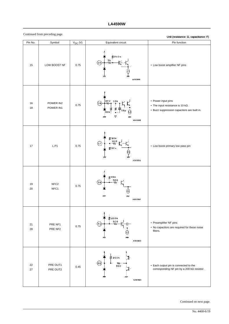
Continued from preceding page.
No. 4468-6/19
LA4590W
Continued on next page.
Pin No. Symbol VDC (V) Equivalent circuit Pin function
15 LOW BOOST NF 0.75
16 POWER IN20.75
18 POWER IN1
17 L.P1 0.75
19 NFC20.75
20 NFC1
21 PRE NF10.75
28 PRE NF2
22 PRE OUT10.45
27 PRE OUT2
• Low boost amplifier NF pins
• Power input pins
• The input resistance is 10 kΩ.
• Buzz suppression capacitors are built in.
• Low boost primary low pass pin
• Preamplifier NF pins
• No capacitors are required for these noisefilters.
• Each output pin is connected to thecorresponding NF pin by a 200 kΩ resistor.
Unit (resistance: Ω, capacitance: F)Unit (resistance: Ω, capacitance: F)
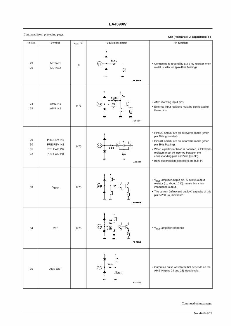
Continued from preceding page.
No. 4468-7/19
LA4590W
Continued on next page.
Pin No. Symbol VDC (V) Equivalent circuit Pin function
23 METAL10
26 METAL2
24 AMS IN10.75
25 AMS IN2
29 PRE REV IN1
30 PRE REV IN20.75
31 PRE FWD IN2
32 PRE FWD IN1
33 VREF 0.75
34 REF 0.75
36 AMS OUT
• Connected to ground by a 3.9 kΩ resistor whenmetal is selected (pin 40 is floating).
• AMS inverting input pins
• External input resistors must be connected tothese pins.
• Pins 29 and 30 are on in reverse mode (whenpin 39 is grounded).
• Pins 31 and 32 are on in forward mode (whenpin 39 is floating).
• When a particular head is not used, 2.2 kΩ biasresistors must be inserted between thecorresponding pins and Vref (pin 33).
• Buzz suppression capacitors are built-in.
• VREF amplifier output pin. A built-in outputresistor (ro, about 10 Ω) makes this a lowimpedance output.
• The current (inflow and outflow) capacity of thispin is 200 µA, maximum.
• VREF amplifier reference
• Outputs a pulse waveform that depends on theAMS IN (pins 24 and 25) input levels.
Unit (resistance: Ω, capacitance: F)Unit (resistance: Ω, capacitance: F)
Continued from preceding page.
No. 4468-8/19
LA4590W
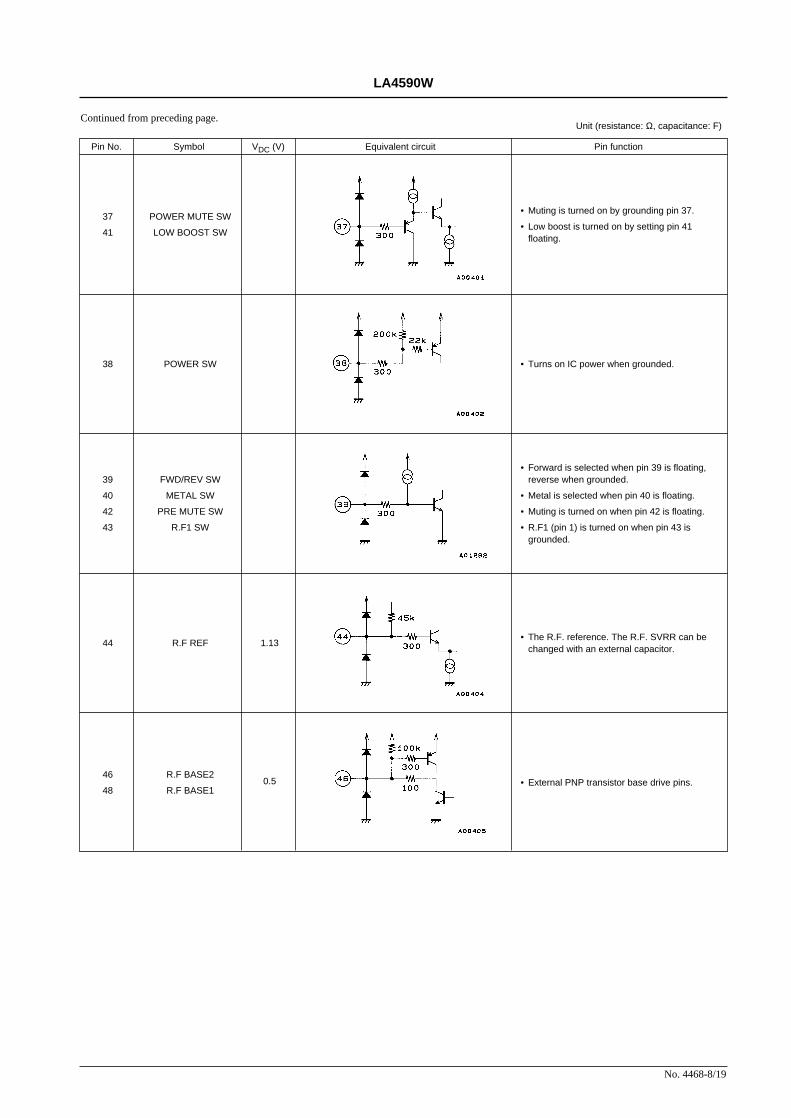
Pin No. Symbol VDC (V) Equivalent circuit Pin function
37 POWER MUTE SW
41 LOW BOOST SW
38 POWER SW
39 FWD/REV SW
40 METAL SW
42 PRE MUTE SW
43 R.F1 SW
44 R.F REF 1.13
46 R.F BASE20.5
48 R.F BASE1
• Muting is turned on by grounding pin 37.
• Low boost is turned on by setting pin 41floating.
• Turns on IC power when grounded.
• Forward is selected when pin 39 is floating,reverse when grounded.
• Metal is selected when pin 40 is floating.
• Muting is turned on when pin 42 is floating.
• R.F1 (pin 1) is turned on when pin 43 isgrounded.
• The R.F. reference. The R.F. SVRR can bechanged with an external capacitor.
• External PNP transistor base drive pins.
Unit (resistance: Ω, capacitance: F)
External Component Functions: Recommended values are indicated in parentheses.
• C1 (1.0 to 10 µF)VREF amplifier reference decoupling capacitorThis capacitor changes the VREF SVRR. Note that the SVRR is degraded as this capacitance decreases.
• C2, C10Playback equalization constants
• C3, C9 (0.47 to 3.3 µF)Preamplifier output capacitors
• C4, C8AMS input high pass filter capacitors
• C5, C7Metal tape equalization constants. (The internal resistance is 3.9 kΩ ±15%.)
• C6 (0.1 to 22 µF)VREF decoupling capacitorUsed for excluding high frequency noise.
• C11, C12 (3.3 to 10 µF)NFC decoupling capacitorsNote that the preamplifier low frequency gain falls as these capacitances are reduced.
• C13, C15 (1.0 to 3.3 µF)Power amplifier input capacitors (Input resistance: 10 kΩ)
• C14, C17Low boost low pass filter capacitorsThe low boost gain can be changed by varying these capacitances.
• C16 (1.0 to 4.7 µF)Boost amplifier NF capacitorNote that the low boost low frequency gain falls as these capacitances are reduced.
• C18, C23, C26 (0.1 to 1.0 µF)Oscillation suppression capacitors
• C19, C22, C25 (3.3 to 10 µF)Power amplifier NF capacitorsNote that the power amplifier low frequency gain falls as these capacitances are reduced.
• C20, C24Loudness high boost capacitorsThe high frequency gain is changed by these capacitances.
• C21 (100 to 2200 pF)Oscillation suppression capacitor
• C27, C29 (4.7 to 10 µF)R.F. output decoupling capacitors (These capacitors also function as power supply capacitors and oscillation suppressioncapacitors.)
• C28 (22 to 220 µF)Power supply capacitors
No. 4468-9/19
LA4590W
• C30 (2.2 to 10 µF)R.F. reference low pass filter capacitorThe R.F. SVRR is changed by this capacitance.
• C31, C32 (6800 pF to 0.22 µF)Switching circuit smoothing capacitors. These capacitances must be adjusted according to the set timing.
• C33, C34 (470 to 1000 pF)Oscillation suppression capacitors used when both the preamplifier and power amplifier are used, i.e., when the volumeis maximum.
• R1, R10Preamplifier gain adjustment
• R2, R9Playback equalization constants
• R3, R8Metal tape equalization constants
• R4, R710 kΩ variable resistors
• R5, R6AMS gain adjustment and high pass filter
• R11, R12, R13Oscillation suppression
• R14, R15 (100 to 430 kΩ)Switching circuit smoothing (discharge resistors)
No. 4468-10/19
LA4590W
Function Descriptions
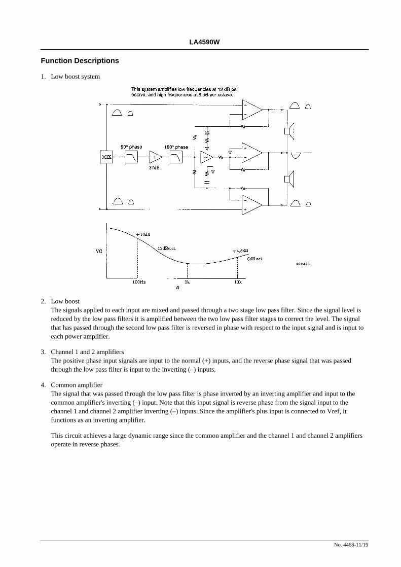
1. Low boost system
2. Low boostThe signals applied to each input are mixed and passed through a two stage low pass filter. Since the signal level isreduced by the low pass filters it is amplified between the two low pass filter stages to correct the level. The signalthat has passed through the second low pass filter is reversed in phase with respect to the input signal and is input toeach power amplifier.
3. Channel 1 and 2 amplifiersThe positive phase input signals are input to the normal (+) inputs, and the reverse phase signal that was passedthrough the low pass filter is input to the inverting (–) inputs.
4. Common amplifierThe signal that was passed through the low pass filter is phase inverted by an inverting amplifier and input to thecommon amplifier's inverting (–) input. Note that this input signal is reverse phase from the signal input to thechannel 1 and channel 2 amplifier inverting (–) inputs. Since the amplifier's plus input is connected to Vref, itfunctions as an inverting amplifier.
This circuit achieves a large dynamic range since the common amplifier and the channel 1 and channel 2 amplifiersoperate in reverse phases.
No. 4468-11/19
LA4590W
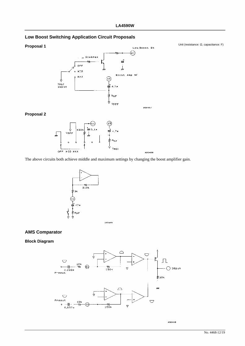
Low Boost Switching Application Circuit Proposals
Proposal 1
Proposal 2
The above circuits both achieve middle and maximum settings by changing the boost amplifier gain.
AMS Comparator
Block Diagram
No. 4468-12/19
LA4590W
Unit (resistance: Ω, capacitance: F)
Function Descriptions
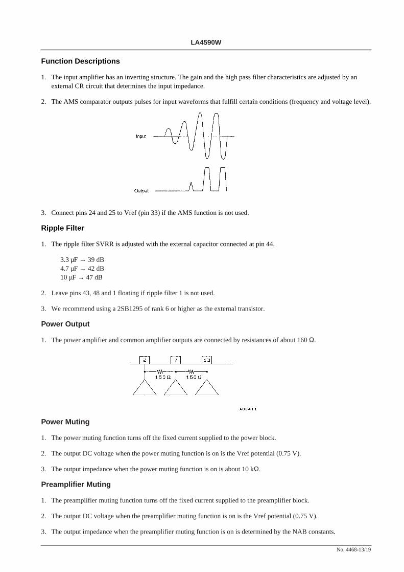
1. The input amplifier has an inverting structure. The gain and the high pass filter characteristics are adjusted by anexternal CR circuit that determines the input impedance.
2. The AMS comparator outputs pulses for input waveforms that fulfill certain conditions (frequency and voltage level).
3. Connect pins 24 and 25 to Vref (pin 33) if the AMS function is not used.
Ripple Filter
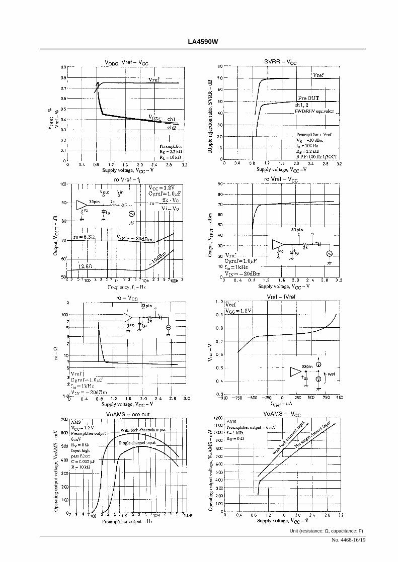
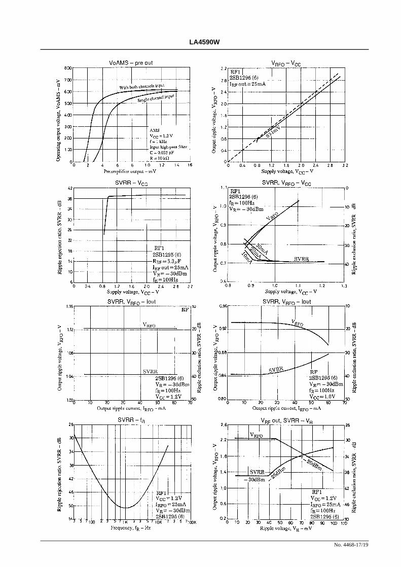
1. The ripple filter SVRR is adjusted with the external capacitor connected at pin 44.
3.3 µF → 39 dB4.7 µF → 42 dB10 µF → 47 dB
2. Leave pins 43, 48 and 1 floating if ripple filter 1 is not used.
3. We recommend using a 2SB1295 of rank 6 or higher as the external transistor.
Power Output
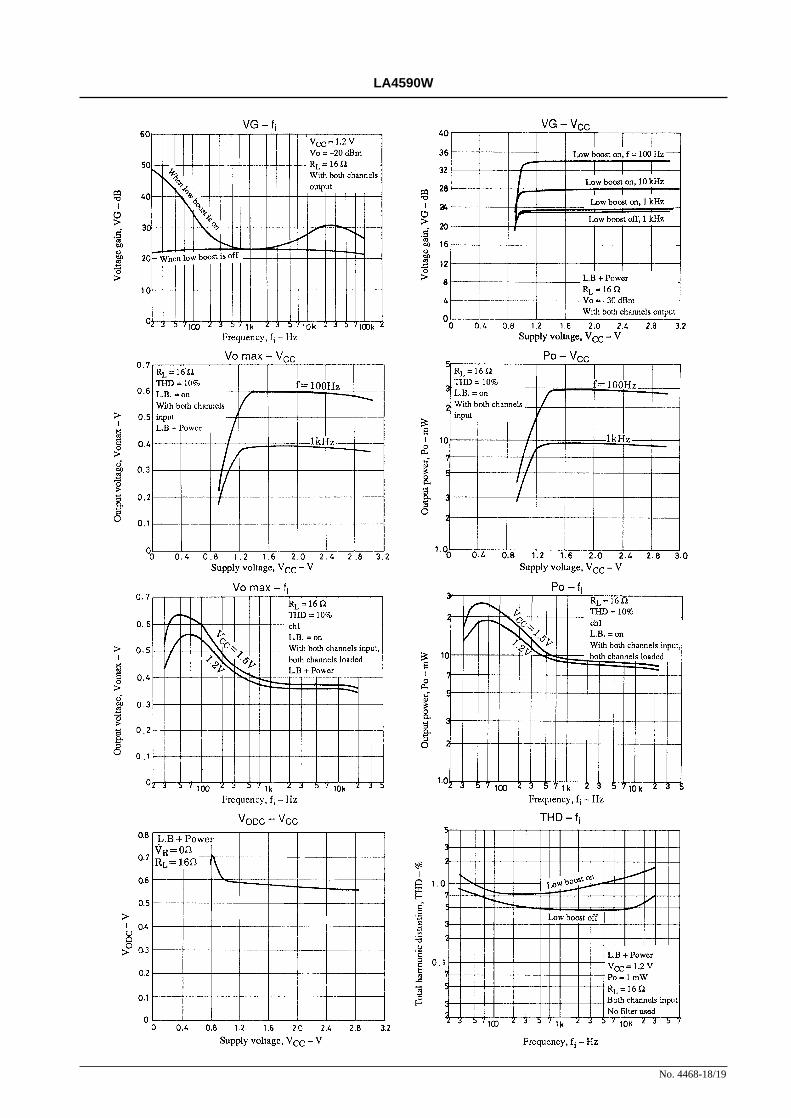
1. The power amplifier and common amplifier outputs are connected by resistances of about 160 Ω.
Power Muting
1. The power muting function turns off the fixed current supplied to the power block.
2. The output DC voltage when the power muting function is on is the Vref potential (0.75 V).
3. The output impedance when the power muting function is on is about 10 kΩ.
Preamplifier Muting
1. The preamplifier muting function turns off the fixed current supplied to the preamplifier block.
2. The output DC voltage when the preamplifier muting function is on is the Vref potential (0.75 V).
3. The output impedance when the preamplifier muting function is on is determined by the NAB constants.
No. 4468-13/19
LA4590W

Switch Pin Equivalent Circuits
1. Power switch pin
2. Power muting and low boost switch pins
3. FWD/REV, METAL, PRE MUTE, R.F1 switches
No. 4468-14/19
LA4590W
The power switch is on when the power switch pin is connectedto ground.
Io = VCC/200 k + VCC – 0.7 V/22 kΩ
Pin 38
VS ≤ 100 mV
The power muting function is turned on when pin 37 is connectedto ground.
The low boost switch is turned on when pin 41 is floating.
Io ≤ 0.1 µA
VS ≤ 80 mV
Note: The smoothing discharge resistor should be 430 kΩ orsmaller.
Reverse is selected when pin 39 is connected to ground.
Metal tape is selected when pin 40 is floating.
Preamplifier muting is turned on when pin 42 is floating.
The ripple filter switch is turned on when pin 43 is grounded.
Pins 39, 40, and 43 Pin 42Io ≤ 7 µA Io ≤ 14 µAVS ≤ 0.5 V VS ≤ 0.5 V

No. 4468-15/19
LA4590W
No. 4468-16/19
LA4590W
Unit (resistance: Ω, capacitance: F)
No. 4468-17/19
LA4590W
No. 4468-18/19
LA4590W
PS No. 4468-19/19
LA4590W
This catalog provides information as of December, 1998. Specifications and information herein aresubject to change without notice.
Specifications of any and all SANYO products described or contained herein stipulate the performance,characteristics, and functions of the described products in the independent state, and are not guaranteesof the performance, characteristics, and functions of the described products as mounted in the customer’sproducts or equipment. To verify symptoms and states that cannot be evaluated in an independent device,the customer should always evaluate and test devices mounted in the customer’s products or equipment.
SANYO Electric Co., Ltd. strives to supply high-quality high-reliability products. However, any and allsemiconductor products fail with some probability. It is possible that these probabilistic failures couldgive rise to accidents or events that could endanger human lives, that could give rise to smoke or fire,or that could cause damage to other property. When designing equipment, adopt safety measures sothat these kinds of accidents or events cannot occur. Such measures include but are not limited to protectivecircuits and error prevention circuits for safe design, redundant design, and structural design.
In the event that any or all SANYO products (including technical data, services) described or containedherein are controlled under any of applicable local export control laws and regulations, such products mustnot be exported without obtaining the export license from the authorities concerned in accordance with theabove law.
No part of this publication may be reproduced or transmitted in any form or by any means, electronic ormechanical, including photocopying and recording, or any information storage or retrieval system,or otherwise, without the prior written permission of SANYO Electric Co., Ltd.
Any and all information described or contained herein are subject to change without notice due toproduct/technology improvement, etc. When designing equipment, refer to the “Delivery Specification”for the SANYO product that you intend to use.
Information (including circuit diagrams and circuit parameters) herein is for example only; it is notguaranteed for volume production. SANYO believes information herein is accurate and reliable, butno guarantees are made or implied regarding its use or any infringements of intellectual property rightsor other rights of third parties.