16-bit, 40ksps low-power sampling adc w/internal ref & parallel
TRANSCRIPT

1FEATURES APPLICATIONS
DESCRIPTION
Successive Approximation RegisterClock
Comparator
CS
CDAC
Buffer
REF
BUF
R1IN8kΩ
Internal+2.5 V Ref
4kΩ
SerialDataOutand
Control
BUSYBUSY
DATACLK
40kΩ
R2IN
EXT/INT
PWRD
SDATACONV
CAP
20kΩR3IN
ADS8513
www.ti.com ...................................................................................................................................................... SLAS486C–JUNE 2007–REVISED JANUARY 2009
16-Bit, 40kSPS, Low-Power Sampling ANALOG-TO-DIGITAL CONVERTERwith Internal Reference and Parallel/Serial Interface
• Industrial Process Control23• 40kSPS Minimum Sampling Rate• Test Equipment• Very Low Power: 24mW Typ• Robotics• ±3.33V, ±5V, ±10V, 4V, and 10V Input Ranges• DSP Servo Control• 89dB SNR with 10kHz Input• Medical Instrumentation• ±2LSB Max INL• Portable Data Acquisition Systems• –1/+2LSB Max DNL, 16-Bit NMC
• ±10mV BPZ, ±2.5ppm/°C BPZ Drift• 89dB Min SINAD, 102dB Min SFDR The ADS8513 is a complete low-power, single 5V• Uses Internal or External 2.5V Reference supply, 16-bit sampling analog-to-digital (A/D)
converter. It contains a complete 16-bit• No External Calibration Resistors Requiredcapacitor-based, successive approximation register• Single 5V Analog Supply:(SAR) A/D converter with sample and hold, clock,
– 32.5mW Max Power Dissipation reference, and serial data interface. The converter– 50µW Max Power-Down Mode can be configured for a variety of input ranges
including ±10V, ±5V, 0V to 10V, and 0.5V to 4.5V. A• SPI™-Compatible Serial Port up to 20MHz,high-impedance, 0.3V to 2.8V input is also availablewith Master/Slave Featurewith input impedance greater than 10MΩ. For most
• Global CONV and 3-Stated Bus for Multi-Chip input ranges, the input voltage can swing to 25V orSimultaneous S/H Operation –25V without damage to the converter.
• Pin-Compatible with 16-Bit ADS7813 and An SPI-compatible serial interface allows data to be12-Bit ADS7812 and ADS8512 synchronized to an internal or external clock. The
• SO-16 Package ADS8513 is specified at 40kSPS sampling rate overthe –40°C to +85°C industrial temperature range.
1
Please be aware that an important notice concerning availability, standard warranty, and use in critical applications of TexasInstruments semiconductor products and disclaimers thereto appears at the end of this data sheet.
2SPI, QSPI are trademarks of Motorola, Inc.3All other trademarks are the property of their respective owners.
PRODUCTION DATA information is current as of publication date. Copyright © 2007–2009, Texas Instruments IncorporatedProducts conform to specifications per the terms of the TexasInstruments standard warranty. Production processing does notnecessarily include testing of all parameters.

ABSOLUTE MAXIMUM RATINGS (1) (2)
ELECTRICAL CHARACTERISTICS
ADS8513
SLAS486C–JUNE 2007–REVISED JANUARY 2009 ...................................................................................................................................................... www.ti.com
These devices have limited built-in ESD protection. The leads should be shorted together or the device placed in conductive foamduring storage or handling to prevent electrostatic damage to the MOS gates.
PACKAGE/ORDERING INFORMATION (1)
MINIMUM NO MINIMUM SPECIFIEDINL MISSING SINAD TEMPERATURE PACKAGE PACKAGE ORDERING TRANSPORT
PRODUCT (LSB) CODES (dB) RANGE LEAD DESIGNATOR NUMBER MEDIA, QTY
ADS8513IBDW Tube, 20ADS8513IB ±2 16-Bit 89 –40°C to +85°C SO-16 DW
ADS8513IBDWR Tape and Reel, 1000
ADS8513IDW Tube, 20ADS8513I ±3 15-Bit 88 –40°C to +85°C SO-16 DW
ADS8513IDWR Tape and Reel, 1000
(1) For the most current package and ordering information, see the Package Option Addendum at the end of this document, or see the TIwebsite at www.ti.com.
over operating free-air temperature range (unless otherwise noted).
PARAMETER UNITR1IN ±25VR2IN ±25V
Analog inputsR3IN ±25VREF VS + 0.3V to GND – 0.3VGND ±0.3V
Ground voltage differencesVS 6V
Digital inputs –0.3V to +VS + 0.3VMaximum junction temperature +165°CStorage temperature range –65°C to +150°CInternal power dissipation 700mWLead temperature (soldering, 1,6 mm from case 10 seconds) +260°C
(1) Stresses above those listed under Absolute Maximum Ratings may cause permanent damage to the device. Exposure to absolutemaximum conditions for extended periods may affect device reliability.
(2) All voltage values are with respect to network ground terminal.
At TA = –40°C to +85°C, fS = 40kSPS, VS = 5V, and using internal reference and fixed resistors, unless otherwise specified.ADS8513I ADS8513IB
PARAMETER TEST CONDITIONS MIN TYP MAX MIN TYP MAX UNIT
Resolution 16 16 Bits
ANALOG INPUT
Voltage ranges see Table 1 see Table 1 V
Impedance see Table 1 see Table 1 Ω
Capacitance 45 45 pF
THROUGHPUT SPEED
Conversion time Acquire and convert 20 20 µs
Complete cycle Acquire and convert 25 25 µs
Throughput rate Acquire and convert 40 40 kSPS
2 Submit Documentation Feedback Copyright © 2007–2009, Texas Instruments Incorporated
Product Folder Link(s): ADS8513

ADS8513
www.ti.com ...................................................................................................................................................... SLAS486C–JUNE 2007–REVISED JANUARY 2009
ELECTRICAL CHARACTERISTICS (continued)At TA = –40°C to +85°C, fS = 40kSPS, VS = 5V, and using internal reference and fixed resistors, unless otherwise specified.
ADS8513I ADS8513IB
PARAMETER TEST CONDITIONS MIN TYP MAX MIN TYP MAX UNIT
DC ACCURACY
INL Integral linearity error –3 3 –2 2 LSB (1)
DNL Differential linearity error –2 3 –1 2 LSB
No missing codes 15 16 Bits
Transition noise (2) 0.6 0.6 LSB
Full-scale error (3) (4) –0.5 0.5 –0.25 0.25 %
Full-scale error drift 10 10 ppm/°C
Full-scale error (3) (4) External 2.5V reference –0.5 0.5 –0.25 0.25 %
Full-scale error drift External 2.5V reference 0.2 0.2 ppm/°C
Bipolar zero error (3) Bipolar ranges –10 10 –10 10 mV
Bipolar zero error drift Bipolar ranges 2.5 2.5 ppm/°C
Unipolar zero error (3) Unipolar ranges –6 6 –6 6 mV
Unipolar zero error drift Unipolar ranges 2.5 2.5 ppm/°C
Recovery time to rated accuracy from 1µF capacitor to CAP 300 300 µspower down (5)
Power-supply sensitivity +4.75V < VS < +5.25V ±8 ±8 LSB
AC ACCURACY
SFDR Spurious-free dynamic range fIN = 1kHz, ±10V 90 100 96 102 dB (6)
THD Total harmonic distortion fIN = 1kHz, ±10V –98 –90 –100 –96 dB
fIN = 1kHz, ±10V 85 89 87 89SINAD Signal-to-(noise+distortion) dB
-60 dB Input 30 32
SNR Signal-to-noise fIN = 1kHz, ±10V 85 89 87 89 dB
Usable bandwidth (7) 130 130 kHz
Full-power bandwidth (–3dB) 600 600 kHz
SAMPLING DYNAMICS
Aperture delay 40 40 ns
Aperture jitter 20 20 ps
Transient response FS step 5 5 µs
Overvoltage recovery (8) 750 750 ns
REFERENCE
Internal reference voltage No load 2.48 2.5 2.52 2.48 2.5 2.52 V
Internal reference source current (must 1 1 µAuse external buffer)
Internal reference drift 8 8 ppm/°C
External reference voltage range for 2.3 2.5 2.7 2.3 2.5 2.7 Vspecified linearity
External reference current drain External 2.5V ref 100 100 µA
(1) LSB means Least Significant Bit. 1 LSB for the ±10V input range is 305µV.(2) Typical rms noise at worst case transitions.(3) As measured with fixed resistors. Adjustable to zero with external potentiometer.(4) Full-scale error is the worst case of –Full Scale or +Full Scale deviation from ideal first and last code transitions, divided by the full-scale
range; includes the effect of offset error. Tested at –40°C to +85°C.(5) Time delay after the ADS8513 is brought out of Power-Down mode until all internal settling occurs and the analog input is acquired to
rated accuracy. A Convert command after this delay will yield accurate results.(6) All specifications in dB are referred to a full-scale input.(7) Usable bandwidth defined as full-scale input frequency at which Signal-to-(Noise + Distortion) degrades to 60dB.(8) Recovers to specified performance after 2 x FS input overvoltage.
Copyright © 2007–2009, Texas Instruments Incorporated Submit Documentation Feedback 3
Product Folder Link(s): ADS8513

ADS8513
SLAS486C–JUNE 2007–REVISED JANUARY 2009 ...................................................................................................................................................... www.ti.com
ELECTRICAL CHARACTERISTICS (continued)At TA = –40°C to +85°C, fS = 40kSPS, VS = 5V, and using internal reference and fixed resistors, unless otherwise specified.
ADS8513I ADS8513IB
PARAMETER TEST CONDITIONS MIN TYP MAX MIN TYP MAX UNIT
DIGITAL INPUTS
VIL Low-level input voltage –0.3 +0.8 –0.3 +0.8 V
VIH High-level input voltage 2.0 VD +0.3 V 2.0 VD +0.3 V V
IIL Low-level input current VIL = 0V ±10 µA
IIH High-level input current VIH = 5V ±10 µA
DIGITAL OUTPUTS
Data format Serial Serial
Data coding Binary twos complement Binary twos complement
VOL Low-level output voltage ISINK = 1.6mA 0.4 0.4 V
VOH High-level output voltage ISOURCE = 500µA 4 4 V
High-Z state,Leakage Current ±1 ±1 µAVOUT = 0V to VS
Output capacitance High-Z state 15 15 pF
DIGITAL TIMING
Bus access time RL = 3.3kΩ, CL = 50pF 83 83 ns
Bus relinquish time RL = 3.3kΩ, CL = 10pF 83 83 ns
POWER SUPPLIES
VS Supply voltage 4.75 5 5.25 4.75 5 5.25 V
IDIG Digital current 0.6 0.6 mA
IANA Analog current 4.2 4.2 mA
VS = 5V, fS = 40kSPS 24 32.5 24 32.5 mWPower dissipation
PWRD and REFD high 50 50 µW
TEMPERATURE RANGE
Specified performance –40 +85 –40 +85 °C
Derated performance –55 +125 –55 +125 °C
Storage temperature –65 +150 –65 +150 °C
θJA Thermal resistance 46 46 °C/W
Table 1. Input RangesCONNECT R1IN CONNECT R2IN CONNECT R3IN INPUT IMPEDANCE
ANALOG INPUT RANGE TO TO TO (kΩ)±10V VIN BUF GND 45.7
0.3125V to 2.8125V VIN VIN VIN > 10,000±5V GND BUF VIN 26.7
0V to 10V BUF GND VIN 26.70V to 4V BUF VIN GND 21.3±3.33V VIN BUF VIN 21.3
0.5V to 4.5V GND VIN GND 21.3
4 Submit Documentation Feedback Copyright © 2007–2009, Texas Instruments Incorporated
Product Folder Link(s): ADS8513

PIN CONFIGURATION
VS
BUSY
CS
DATACLK
R1IN
GND
BUF
CAP
1
2
3
4
5
6
7
8
16
15
14
13
12
11
10
9
R2IN
REF
EXT/INT
DATA
PWRD
R3IN
GND
CONV
ADS8513
www.ti.com ...................................................................................................................................................... SLAS486C–JUNE 2007–REVISED JANUARY 2009
DW PACKAGESO-16
(TOP VIEW)
Pin AssignmentsPIN DIGITAL
NAME NO. I/O DESCRIPTIONR1IN 1 Analog input. See Table 1 and Table 3.R2IN 3 Analog input. See Table 1 and Table 3.R3IN 4 Analog input. See Table 1 and Table 3.BUF 5 Reference buffer output. Connect to R1IN, R2IN, or R3IN as needed
6 Reference buffer compensation node. Decouple to ground with a 1-µF tantalum capacitor in parallelCAP with a 0.01µF ceramic capacitor.7 Reference input/output. Outputs internal 2.5V reference via a series 4kΩ resistor. Decouple this
REF voltage with a 1µF to 2.2µF tantalum capacitor to ground. If an external reference voltage is appliedto this pin, it overrides the internal reference.
9 I/O Data clock pin. With EXT/INT low, this pin is an output and provides the synchronous clock for theDATACLK serial data. The output is 3-stated when CS is high. With EXT/INT high, this pin is an input and the
serial data clock must be provided externally.10 O Serial data output. The serial data are always the result of the last completed conversion and are
DATA synchronized to DATACLK. If DATACLK is from the internal clock (EXT/INT low), the serial data arevalid on both the rising and falling edges of DATACLK. DATA is 3-stated when CS is high.
11 I External/Internal DATACLK pin. Selects the source of the synchronous clock for serial data. If high,the clock must be provided externally. If low, the clock is derived from the internal conversion clock.EXT/INT Note that the clock used to time the conversion is always interna,l regardless of the status ofEXT/INT.
12 Convert input. A falling edge on this input puts the internal sample/hold into the hold state and startsa conversion regardless of the state of CS. If a conversion is already in progress, the falling edge isCONV ignored. If EXT/INT is low, data from the previous conversion are serially transmitted during thecurrent conversion.
13 I Chip select. This input 3-states all outputs when high and enables all outputs when low, includingCS DATA, BUSY, and DATACLK (when EXT/INT is low). Note that a falling edge on CONV initiates a
conversion even when CS is high.14 O Busy output. When a conversion starts, BUSY goes low and remains low throughout the conversion.
BUSY If EXT/INT is low, data are serially transmitted while BUSY is low. BUSY is 3-stated when CS ishigh.
15 I Power-down input. When high, the majority of the ADS8513 circuitry is placed in a low-power modeand power consumption is significantly reduced. (The ADS7813 requires CONV be taken low beforePWRD goes low in order to achieve the lowest power consumption. This is not necessary for thePWRD ADS8513 and it does not cause interference if performed.) The time required for the ADS7813 toreturn to normal operation after power down depends on a number of factors. Consult the Chapter 0section for more information.
GND 2, 8 Ground.16 +5V supply input. For best performance, decouple to ground with a 0.1µF ceramic capacitor inVS parallel with a 10µF tantalum capacitor.
Copyright © 2007–2009, Texas Instruments Incorporated Submit Documentation Feedback 5
Product Folder Link(s): ADS8513

TYPICAL CHARACTERISTICS
4
4.5
5
5.5
6
-40 -25 -10 5 20 35 50 65 80 95 110 125
T - Free-Air Temperature - ºCA
I-
Po
wer
Su
pp
ly C
urr
en
t -
mA
CC
2.480
2.485
2.490
2.495
2.500
2.505
2.510
2.515
2.520
-40 -25 -10 5 20 35 50 65 80 95 110125
T - Free-Air Temperature - ºCA
V-
Inte
rnal R
efe
ren
ce V
olt
ag
e -
Vre
f
4
4.5
5
5.5
6
10 20 30 40
f - Sampling Frequency - kHzs
I-
Po
wer
Su
pp
ly C
urr
en
t -
mA
CC
-0.15
-0.1
-0.05
0
0.05
0.1
0.15
T - Free-Air Temperature - CA °
-45 -30 -15 0 15 45 60 75 9030 105 120
Bip
ola
r N
eg
ati
ve F
ull-S
cale
Err
or
- %
FS
R
20 V Bipolar Range,
Drift = 12.2 ppm/ C°
-6
-3
0
3
6
9
Bip
ola
rO
ffs
et
Err
or
-m
V
-45 -30 -15 0 15 45 60 75 9030 105 120
T - Free-Air Temperature - CA °
20 V Bipolar Range,
Drift = 1.5 ppm/ C°
-0.1
-0.05
0
0.05
0.1
T - Free-Air Temperature - CA °
-45 -30 -15 0 15 45 60 75 9030 105 120
20 V Bipolar Range,
Drift = 9.2 ppm/ C°
Bip
ola
r P
osit
ive F
ull-S
cale
E
rro
r -
%F
SR
-0.2
-0.15
-0.1
-0.05
0
0.05
0.1
T - Free-Air Temperature - CA °
-45 -30 -15 0 15 45 60 75 9030 105 120
Bip
ola
r N
eg
ati
ve F
ull-S
cale
Err
or
- %
FS
R 10 V Bipolar Range,
Drift = 13.5 ppm/ C°
-0.05
0
0.05
0.1
0.15
0.2
T - Free-Air Temperature - CA °
-45 -30 -15 0 15 45 60 75 9030 105 120
10 V Bipolar Range,
Drift = 10.3 ppm/ C°
Bip
ola
r P
osit
ive F
ull-S
cale
Err
or
- %
FS
R
-6
-3
0
3
6
9
T - Free-Air Temperature - CA °
-45 -30 -15 0 15 45 60 75 9030 105 120
Bip
ola
r O
ffset
Err
or
- m
V
10 V Bipolar Range,
Drift = 0.8 ppm/ C°
ADS8513
SLAS486C–JUNE 2007–REVISED JANUARY 2009 ...................................................................................................................................................... www.ti.com
POWER-SUPPLY CURRENT INTERNAL REFERENCE VOLTAGE POWER-SUPPLY CURRENTvs vs vs
FREE-AIR TEMPERATURE FREE-AIR TEMPERATURE SAMPLING FREQUENCY
Figure 1. Figure 2. Figure 3.
BIPOLAR POSITIVE FULL-SCALE BIPOLAR NEGATIVE FULL-SCALEBIPOLAR OFFSET ERROR ERROR ERROR
vs vs vsFREE-AIR TEMPERATURE FREE-AIR TEMPERATURE FREE-AIR TEMPERATURE
Figure 4. Figure 5. Figure 6.
BIPOLAR POSITIVE FULL-SCALE BIPOLAR NEGATIVE FULL-SCALEBIPOLAR OFFSET ERROR ERROR ERROR
vs vs vsFREE-AIR TEMPERATURE FREE-AIR TEMPERATURE FREE-AIR TEMPERATURE
Figure 7. Figure 8. Figure 9.
6 Submit Documentation Feedback Copyright © 2007–2009, Texas Instruments Incorporated
Product Folder Link(s): ADS8513

-2
-1
0
1
2
T - Free-Air Temperature - CA °
-45 -30 -15 0 15 45 60 75 9030 105 120
Un
ipo
lar
Off
set
Err
or
- m
V
4 V Unipolar Range,
Drift = 2.8 ppm/ C°
-2
-1
0
1
2
T - Free-Air Temperature - CA °
-45 -30 -15 0 15 45 60 75 9030 105 120
Un
ipo
lar
Off
set
Err
or
- m
V
10 V Unipolar Range,
Drift = 2.8 ppm/ C°
0.15
0.2
T - Free-Air Temperature - CA °
-45 -30 -15 0 15 45 60 75 9030 105 120
Un
ipo
lar
Po
sit
ive
Fu
ll-S
ca
le E
rro
r -
%F
SR
4 V Unipolar Range,Drift = 0.1 ppm/°C
0.15
0.2
T - Free-Air Temperature - CA °
-45 -30 -15 0 15 45 60 75 9030 105 120
Un
ipo
lar
Po
sit
ive F
ull-S
cale
Err
or
- %
FS
R
10 V Unipolar Range,
Drift = 0.4 ppm/ C°f = 10 kHz, 0 dBi
80
85
90
95
100
105
110
-50 -25 0 25 50 75 100 125
SF
DR
- S
pu
rio
us F
ree D
yn
am
ic R
an
ge -
dB
T - Free-Air Temperature - ºCA
-50 -25 0 25 50 75 100 125
-110
-105
-100
-95
-90
-85
-80
TH
D -
To
tal
Ha
rmo
nic
Dis
tort
ion
- d
B
T - Free-Air Temperature - ºCA
f = 10 kHz, 0 dBi
10
20
30
40
50
60
70
80
90
100
0 2 4 6 8 10 12 14 16 18 20
f - Frequency - kHz
SIN
AD
- S
ign
al-
To
-No
ise +
Dis
tort
ion
- d
B
-20 dB
-60 dB
0 dB
80
85
90
95
100
105
110
-50 -25 0 25 50 75 100 125
SN
R -
Sig
nal-
To
-No
ise R
ati
o -
dB
T - Free-Air Temperature - ºCA
f = 10 kHz, 0 dBi
80
85
90
95
100
105
110
-50 -25 0 25 50 75 100 125
SIN
AD
- S
ign
al-
To
-No
ise +
Dis
tort
ion
- d
B
T - Free-Air Temperature - ºCA
f = 10 kHz, 0 dBi
ADS8513
www.ti.com ...................................................................................................................................................... SLAS486C–JUNE 2007–REVISED JANUARY 2009
TYPICAL CHARACTERISTICS (continued)
UNIPOLAR POSITIVE FULL-SCALEUNIPOLAR OFFSET ERROR ERROR UNIPOLAR OFFSET ERROR
vs vs vsFREE-AIR TEMPERATURE FREE-AIR TEMPERATURE FREE-AIR TEMPERATURE
Figure 10. Figure 11. Figure 12.
UNIPOLAR POSITIVE FULL-SCALEERROR SPURIOUS FREE DYNAMIC RANGE TOTAL HARMONIC DISTORTION
vs vs vsFREE-AIR TEMPERATURE FREE-AIR TEMPERATURE FREE-AIR TEMPERATURE
Figure 13. Figure 14. Figure 15.
SIGNAL-TO-NOISE RATIO SIGNAL-TO-NOISE + DISTORTION SIGNAL-TO-NOISE + DISTORTIONvs vs vs
FREE-AIR TEMPERATURE FREE-AIR TEMPERATURE FREQUENCY
Figure 16. Figure 17. Figure 18.
Copyright © 2007–2009, Texas Instruments Incorporated Submit Documentation Feedback 7
Product Folder Link(s): ADS8513

f = 0 dBi
60
70
80
90
100
0 1 10 100 1000
f - Frequency - kHz
SN
R -
Sig
nal-
To
-No
ise R
ati
o -
dB
60
70
80
90
100
0 1 10 100 1000
SIN
AD
- S
ign
al-
To
-No
ise +
Dis
tort
ion
- d
B
f - Frequency - kHz
f = 0 dBi
f = 10 kHz, 0 dBi
75
80
85
90
95
100
-50 -25 0 25 50 75 100 125
f = 20 kHzs
f = 30 kHzs
f = 40 kHzs
f = 10 kHzs
T - Free-Air Temperature - ºCA
SIN
AD
- S
ign
al-
To
-No
ise
+ D
isto
rtio
n -
dB
f = 10 kHz, 0 dBi
80
85
90
95
100
105
110
0 1 2 3 4 5 6 7 8 9 10
SF
DR
- S
pu
rio
us F
ree D
yn
am
ic R
an
ge -
dB
ESR - W
70
80
90
100
110
0 1 10 100 1000
SF
DR
- S
pu
rio
us
Fre
e D
yn
am
ic R
an
ge
- d
B
f - Frequency - kHz
f = 0 dBi
-120
-110
-100
-90
-80
-70
0 1 10 100 1000
TH
D -
To
tal H
arm
on
ic D
isto
rtio
n -
dB
f - Frequency - kHz
f = 0 dBi
f = 10 kHz, 0 dBi
0 1 2 3 4 5 6 7 8 9 10
-110
-105
-100
-95
-90
-85
-80
TH
D -
To
tal
Ha
rm
on
ic D
isto
rti
on
- d
B
ESR - W
f = 10 kHz, 0 dBi
80
85
90
95
100
105
110
0 1 2 3 4 5 6 7 8 9 10
SN
R -
Sig
nal-
To
-No
ise R
ati
o -
dB
ESR - W
f = 10 kHz, 0 dBi
80
85
90
95
100
105
110
0 1 2 3 4 5 6 7 8 9 10
SIN
AD
- S
ign
al-
To
-No
ise +
Dis
tort
ion
- d
B
ESR - W
ADS8513
SLAS486C–JUNE 2007–REVISED JANUARY 2009 ...................................................................................................................................................... www.ti.com
TYPICAL CHARACTERISTICS (continued)
SIGNAL-TO-NOISE + DISTORTION SIGNAL-TO-NOISE RATIO SIGNAL-TO-NOISE + DISTORTIONvs vs vs
FREE-AIR TEMPERATURE FREQUENCY FREQUENCY
Figure 19. Figure 20. Figure 21.
SPURIOUS FREE DYNAMIC RANGE TOTAL HARMONIC DISTORTION SPURIOUS FREE DYNAMIC RANGEvs vs vs
FREQUENCY FREQUENCY ESR
Figure 22. Figure 23. Figure 24.
TOTAL HARMONIC DISTORTION SIGNAL-TO-NOISE RATIO SIGNAL-TO-NOISE + DISTORTIONvs vs vs
ESR ESR ESR
Figure 25. Figure 26. Figure 27.
8 Submit Documentation Feedback Copyright © 2007–2009, Texas Instruments Incorporated
Product Folder Link(s): ADS8513
17.2
17.3
17.4
17.5
17.6
17.7
17.8
-50 -25 0 25 50 75 100 125
t-
Co
nvers
ion
Tim
e -
CO
NV
ER
Tμ
s
T - Free-Air Temperature - ºCA
Silicon tested under10 V Bipolar range
-65
-60
-55
-50
-45
-40
-35
-30
-25
-20
10 100 1k 10 k 100 k 1 M
Ou
tpu
t R
eje
cti
on
- d
B
Power Supply Ripple Frequency - Hz
-3
-2
-1
0
1
2
3
INL
- L
SB
s
81920 16384 24576 32768 40960 49152 57344 65535
Code
-3
-2
-1
0
1
2
3
0 8192 16384 24576 32768 40960 49152 57344
Code
DN
L-
LS
Bs
65535
ADS8513
www.ti.com ...................................................................................................................................................... SLAS486C–JUNE 2007–REVISED JANUARY 2009
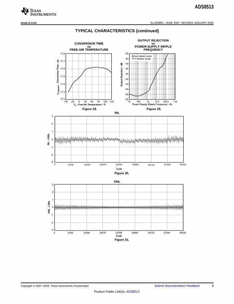
TYPICAL CHARACTERISTICS (continued)
OUTPUT REJECTIONCONVERSION TIME vs
vs POWER-SUPPLY RIPPLEFREE-AIR TEMPERATURE FREQUENCY
Figure 28. Figure 29.INL
Figure 30.
DNL
Figure 31.
Copyright © 2007–2009, Texas Instruments Incorporated Submit Documentation Feedback 9
Product Folder Link(s): ADS8513

8192 Point FFT; f = 20 kHz, 0 dBi
-130
-120
-110
-100
-90
-80
-70
-60
-50
-40
-30
-20
-10
0
0 5 10 15 20
f - Frequency - kHz
Am
plitu
de -
dB
8192 Point FFT; f = 10 kHz, 0 dBi
-130
-120
-110
-100
-90
-80
-70
-60
-50
-40
-30
-20
-10
0
0 5 10 15 20
f - Frequency - kHz
Am
pli
tud
e -
dB
ADS8513
SLAS486C–JUNE 2007–REVISED JANUARY 2009 ...................................................................................................................................................... www.ti.com
TYPICAL CHARACTERISTICS (continued)FFT
Figure 32.
FFT
Figure 33.
10 Submit Documentation Feedback Copyright © 2007–2009, Texas Instruments Incorporated
Product Folder Link(s): ADS8513

BASIC OPERATION
INTERNAL DATACLK
1
2
3
4
5
6
7
8
R1IN
GND
R2IN
R3IN
BUF
CAP
REF
GND
VS
PWRD
BUSY
CS
CONV
EXT/INT
DATA
DATACLK
16
15
14
13
12
11
10
9
ADS8513
±10V +5V
C3
1µF
C4
0.01µF
C1
0.1µF
C2
10µF
C5
1µF
+
+
Convert Pulse
40ns min
+
Frame Sync (optional)
EXTERNAL DATACLK
1
2
3
4
5
6
7
8
R1IN
GND
R2IN
R3IN
BUF
CAP
REF
GND
VS
PWRD
BUSY
CS
CONV
EXT/INT
DATA
DATACLK
16
15
14
13
12
11
10
9
ADS8513
±10V
NOTE: (1) Tie to GND if the outputs will always be active.CS
+5V
+5V
C1
0.1µF
C2
10µF
C5
1µF
+
Convert Pulse
40ns min
+
Interrupt (optional)
External Clock
Chip Select (optional(1))
C3
1µF
C4
0.01µF
+
ADS8513
www.ti.com ...................................................................................................................................................... SLAS486C–JUNE 2007–REVISED JANUARY 2009
Figure 34 shows a basic circuit to operate the ADS8513 with a ±10V input range using an internal DATACLK. Tobegin a conversion and serial transmission of the results from the previous conversion, a falling edge must beprovided to the CONV input. BUSY goes low to indicate that a conversion has started, and stays low until theconversion is complete. During the conversion, the results of the previous conversion are transmitted via DATAwhile DATACLK provides the synchronous clock for the serial data. The data format is 16-bit, binary twoscomplement, MSB first. Each data bit is valid on both the rising and falling edge of DATACLK. BUSY is lowduring the entire serial transmission and can be used as a frame synchronization signal.
Figure 34. Basic Operating Circuit, ±10V Input Range, Internal DATACLK
Figure 35 shows another basic circuit to operate the ADS8513 with a ±10V input rangeusing an externalDATACLK. To begin a conversion, a falling edge must be provided to the CONV input. BUSY goes low toindicate that a conversion has started,and stays low until the conversion is complete. Just before BUSY risesnear the end of the conversion, the conversion result held in the internal working register is transferred to theinternal shift register.
The internal shift register is clocked via the DATACLK input. The recommended method of reading theconversion result is to provide the serial clock after the conversion has completed. See External DATACLK underthe Reading Data section of this data sheet for more information.
Figure 35. Basic Operating Circuit, ±10V Input Range, External DATACLK
Copyright © 2007–2009, Texas Instruments Incorporated Submit Documentation Feedback 11
Product Folder Link(s): ADS8513

STARTING A CONVERSION
Convert ConvertAcquire AcquireMODE
BUSY
CONV
t3
t2
t1
t5t4
t7
t6
t8 t10
t11t9
ADS8513
SLAS486C–JUNE 2007–REVISED JANUARY 2009 ...................................................................................................................................................... www.ti.com
If a conversion is not currently in progress, a falling edge on the CONV input places the sample-and-hold into thehold mode and begins a conversion, as shown in Figure 36 according to the timing shown in Table 2. During theconversion, the CONV input is ignored. Starting a conversion does not depend on the state of CS. A conversioncan be started once every 25µs (40kSPS maximum conversion rate). There is no minimum conversion rate.
Figure 36. Basic Conversion Timing
Table 2. Conversion and Data Timing, TA = –40°C to +85°CSYMBOL DESCRIPTION MIN TYP MAX UNITS
t1 Conversion plus acquisition time 25 µst2 CONV low to all digital inputs stable 19 µst3 CONV low to initiate a conversion 0.04 12 µst4 BUSY rising to any digital input active 5 nst5 CONV high prior to start of conversion (CONV high time) 15 nst6 BUSY low 18 20 µst7 CONV low to BUSY low 12 20 nst8 Aperture delay (CONV falling edge to actual conversion start) 5 nst9 Conversion time 18 20 µst10 Conversion complete to BUSY rising 90 nst11 Acquisition time 7 µst12 CONV low to rising edge of first internal DATACLK 2.0 µst13 Internal DATACLK high 300 410 425 nst14 Internal DATACLK low 300 410 425 nst15 Internal DATACLK period 0.6 0.82 0.85 µst16 DATA valid to internal DATACLK rising 150 204 nst17 Internal DATACLK falling to DATA not valid 150 208 nst18 Falling edge of last DATACLK to BUSY rising 4.4 5 µst19 External DATACLK rising to DATA not valid 4 14 nst20 External DATACLK rising to DATA valid 2 12 20 nst21 External DATACLK high 15 nst22 External DATACLK low 15 nst23 External DATACLK period 35 nst24 CONV low to external DATACLK active 15 nst25 External DATACLK low or CS high to BUSY rising 5 µst26 CS low to digital outputs enabled 15 nst27 CS high to digital outputs disabled 15 ns
12 Submit Documentation Feedback Copyright © 2007–2009, Texas Instruments Incorporated
Product Folder Link(s): ADS8513
ADS8513
www.ti.com ...................................................................................................................................................... SLAS486C–JUNE 2007–REVISED JANUARY 2009
Even though the CONV input is ignored while a conversion is in progress, this input should be held static duringthe conversion period. Transitions on this digital input can easily couple into sensitive analog portions of theconverter, adversely affecting the conversion results (see the Sensitivity to External Digital Signals section of thisdata sheet for more information).
Ideally, the CONV input should go low and remain low throughout the conversion. It should return high sometimeafter BUSY goes high. In addition, it should be high before the start of the next conversion for a minimum timeperiod given by t5. This period ensures that the digital transition on the CONV input does not affect the signal thatis acquired for the next conversion.
An acceptable alternative is to return the CONV input high as soon after the start of the conversion as possible.For example, a negative-going pulse 100ns wide would make a good CONV input signal. It is stronglyrecommended that from time t2 after the start of a conversion until BUSY rises, the CONV input should be heldstatic (either high or low). During this time, the converter is more sensitive to external noise.
Copyright © 2007–2009, Texas Instruments Incorporated Submit Documentation Feedback 13
Product Folder Link(s): ADS8513

READING DATA
QD
S0
Q
Update of the shift
register occurs just prior
to RisingBUSY (1)
D
S1
QD
S2
QD
S14
QD
S15
Q
Shift Register
Working Register
Converter Core
D
SOUT
QD
W0
Q
Each flip-flop in the
working register is
latched as the
conversion proceeds
D
W1
QD
W2
QD
W14
QD
W15
• • •
Delay
DATA
BUSY
DATACLK
CDAC
Control LogicClock
REF
EXT/INT
CONV
CS
NOTE: (1) If EXT/ is HIGH (external clock), DATACLK is HIGH, and is LOW duringINT CS
this time, the shift register will not be updated and the conversion result will be lost.
ADS8513
SLAS486C–JUNE 2007–REVISED JANUARY 2009 ...................................................................................................................................................... www.ti.com
The ADS8513 digital output is in Binary Two’s Complement (BTC) format. Table 3 shows the relationshipbetween the digital output word and the analog input voltage under ideal conditions.
Table 3. Output Codes and Ideal Input VoltagesDESCRIPTION ANALOG INPUT RANGE DIGITAL OUTPUT
Full-scale range ±10V 0.5V to 4.5V BINARY TWOS COMPLEMENT
Least significant bit (LSB) 305µV 61µV BINARY CODE HEX CODE
+Full-scale (FS – 1LSB) 9.999695V 4.499939V 0111 1111 1111 1111 7FFF
Midscale 0V 2.5V 0000 0000 0000 0000 0000
One LSB below midscale –305µV 2.499939µV 1111 1111 1111 1111 FFFF
–Full-scale –10V 0.5V 1000 0000 0000 0000 8000
Figure 37 shows the relationship between the various digital inputs, digital outputs, and internal logic of theADS8513. Figure 38 illustrates when the internal shift register of the ADS8513 is updated and how this updaterelates to a single conversion cycle. Together, these two figures define a very important aspect of the ADS8513:the conversion result is not available until after the conversion is complete. The implications of thisprotocol are discussed in the following sections.
Figure 37. Block Diagram of the ADS8513 Digital Inputs and Outputs
14 Submit Documentation Feedback Copyright © 2007–2009, Texas Instruments Incorporated
Product Folder Link(s): ADS8513

CONV
t6 – t25
t25
BUSY
NOTE: Update of the internal shift register occurs in the
shaded region. If EXT/INT is HIGH, then DATACLK
must be LOW or CS must be HIGH during this time.
INTERNAL DATACLK
t17
DATACLK
BUSY
CONV
t1
t12 t
18
t16
t14
t13
t15
1 12 3 14 15 16
DATA MSB Bit 14 Bit 13 Bit 2 Bit 1 LSB MSB
EXTERNAL DATACLK
ADS8513
www.ti.com ...................................................................................................................................................... SLAS486C–JUNE 2007–REVISED JANUARY 2009
Figure 38. Shift Register Update Timing
With EXT/INT tied low, the result from conversion ‘n’ is serially transmitted during conversion ‘n+1’, as shown inFigure 39 and with the timing given in Table 2. Serial transmission of data occurs only during a conversion.When a transmission is not in progress, DATA and DATACLK are low.
Figure 39. Serial Data Timing, Internal Clock (EXT/INT and CS Low)
During the conversion, the results of the previous conversion are transmitted via DATA, while DATACLKprovides the synchronous clock for the serial data. The data format is 16-bit, Binary Two’s Complement, MSBfirst. Each data bit is valid on both the rising and falling edges of DATACLK. BUSY is low during the entire serialtransmission and can be used as a frame synchronization signal.
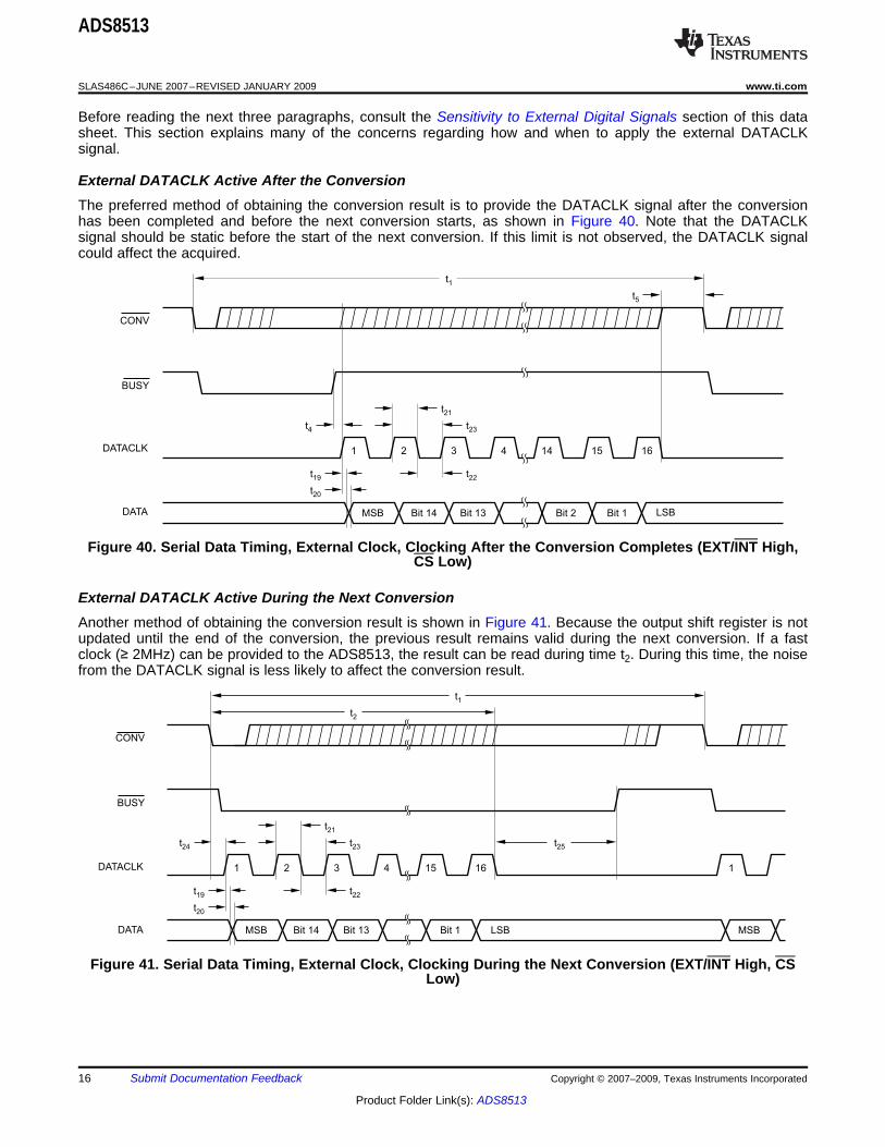
With EXT/INT tied high, the result from conversion ‘n’ is clocked out after the conversion has completed, duringthe next conversion (‘n+1’), or a combination of these two. Figure 40 shows the case of reading the conversionresult after the conversion is complete. Figure 41 describes reading the result during the next conversion.Figure 42 combines the important aspects of Figure 40 and Figure 41 for reading part of the result after theconversion is complete and the balance during the next conversion.
The serial transmission of the conversion result is initiated by a rising edge on DATACLK. The data format is16-bit, Binary Two’s Complement, MSB first. Each data bit is valid on the falling edge of DATACLK. In somecases, it might be possible to use the rising edge of the DATACLK signal. However, one extra clock period (notshown in Figure 40, Figure 41, and Figure 42) is needed for the final bit.
The external DATACLK signal must be low or CS must be high before BUSY rises (see time t25 in Figure 41 andFigure 42). If this limit is not observed during this time, the output shift register of the ADS8513 is not updatedwith the conversion result. Instead, the previous contents of the shift register remain and the new result is lost.
Copyright © 2007–2009, Texas Instruments Incorporated Submit Documentation Feedback 15
Product Folder Link(s): ADS8513
BUSY
CONV
t1
t5
DATACLK
t4
t23
t22
t21
t20
t19
1 2 3 4 14 15 16
DATA MSB Bit 14 Bit 13 Bit 2 Bit 1 LSB
3 4
BUSY
CONV
t2
t1
DATACLK
t24
t25
t23
t22
t21
t20
t19
1 12 15 16
DATA MSB Bit 14 Bit 13 Bit 1 LSB MSB
ADS8513
SLAS486C–JUNE 2007–REVISED JANUARY 2009 ...................................................................................................................................................... www.ti.com
Before reading the next three paragraphs, consult the Sensitivity to External Digital Signals section of this datasheet. This section explains many of the concerns regarding how and when to apply the external DATACLKsignal.
External DATACLK Active After the ConversionThe preferred method of obtaining the conversion result is to provide the DATACLK signal after the conversionhas been completed and before the next conversion starts, as shown in Figure 40. Note that the DATACLKsignal should be static before the start of the next conversion. If this limit is not observed, the DATACLK signalcould affect the acquired.
Figure 40. Serial Data Timing, External Clock, Clocking After the Conversion Completes (EXT/INT High,CS Low)
External DATACLK Active During the Next ConversionAnother method of obtaining the conversion result is shown in Figure 41. Because the output shift register is notupdated until the end of the conversion, the previous result remains valid during the next conversion. If a fastclock (≥ 2MHz) can be provided to the ADS8513, the result can be read during time t2. During this time, the noisefrom the DATACLK signal is less likely to affect the conversion result.
Figure 41. Serial Data Timing, External Clock, Clocking During the Next Conversion (EXT/INT High, CSLow)
16 Submit Documentation Feedback Copyright © 2007–2009, Texas Instruments Incorporated
Product Folder Link(s): ADS8513

BUSY
CONV
t24
t4
t5
DATACLK
t25
1 2 n n+1 15 16
DATA MSB Bit 14 Bit n Bit n-1 Bit 1 LSB
CHIP SELECT
ActiveHI-Z HI-ZBUSY, DATA,
DATACLK (1)
CS
t27t26
NOTE: (1) DATACLK is an output only when EXT/INT is LOW.
ADS8513
www.ti.com ...................................................................................................................................................... SLAS486C–JUNE 2007–REVISED JANUARY 2009
External DATACLK Active After the Conversion and During the Next ConversionFigure 42 shows a method that combines the two previous approaches. This method works very well formicrocontrollers that do serial transfers eight bits at a time and for slower microcontrollers. For example, if thefastest serial clock that the microcontroller can produce is 1µs, the approach shown in Figure 40 would result in adiminished throughput (26kSPS maximum conversion rate). The method described in Figure 41 could not beused without risk of affecting the conversion result (the clock would have to be active after time t2). Therefore, theapproach in Figure 42 results in an improved throughput rate (33kSPS maximum with a 1µs clock), andDATACLK is not active after time t2.
Figure 42. Serial Data Timing, External Clock, Clocking After the Conversion Completes and During theNext Conversion (EXT/INT High, CS Low)
The CS input allows the digital outputs of the ADS8513 to be disabled and gates the external DATACLK signalwhen EXT/INT is high. See Figure 43 for the enable and disable time associated with CS and Figure 37 for alogic diagram of the ADS8513. The digital outputs can be disabled at any time.
Note that a conversion is initiated on the falling edge of CONV even if CS is high. If the EXT/INT input is low(internal DATACLK) and CS is high during the entire conversion, the previous conversion result is lost (that is,the serial transmission occurs but DATA and DATACLK are disabled).
Figure 43. Enable and Disable Timing for Digital Outputs
Copyright © 2007–2009, Texas Instruments Incorporated Submit Documentation Feedback 17
Product Folder Link(s): ADS8513
ANALOG INPUT
OPA627
GND
GND
GND
GND
Pin 1Pin 7
−Pin 2
+Pin3
Pin4
Pin 6
−15 V
+15 V2.2F
100nF
2k
22pF
2k
22pF
2.2F
2.2F100nF
2.2F
R1IN
GND
R2IN
R3IN
CAP
REF
ADS8513
OPA132or
GND
VIN
ADS8513
SLAS486C–JUNE 2007–REVISED JANUARY 2009 ...................................................................................................................................................... www.ti.com
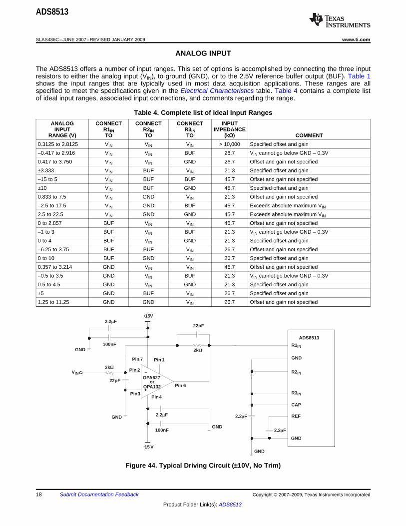
The ADS8513 offers a number of input ranges. This set of options is accomplished by connecting the three inputresistors to either the analog input (VIN), to ground (GND), or to the 2.5V reference buffer output (BUF). Table 1shows the input ranges that are typically used in most data acquisition applications. These ranges are allspecified to meet the specifications given in the Electrical Characteristics table. Table 4 contains a complete listof ideal input ranges, associated input connections, and comments regarding the range.
Table 4. Complete list of Ideal Input RangesANALOG CONNECT CONNECT CONNECT INPUT
INPUT R1IN R2IN R3IN IMPEDANCERANGE (V) TO TO TO (kΩ) COMMENT
0.3125 to 2.8125 VIN VIN VIN > 10,000 Specified offset and gain–0.417 to 2.916 VIN VIN BUF 26.7 VIN cannot go below GND – 0.3V0.417 to 3.750 VIN VIN GND 26.7 Offset and gain not specified±3.333 VIN BUF VIN 21.3 Specified offset and gain–15 to 5 VIN BUF BUF 45.7 Offset and gain not specified±10 VIN BUF GND 45.7 Specified offset and gain0.833 to 7.5 VIN GND VIN 21.3 Offset and gain not specified–2.5 to 17.5 VIN GND BUF 45.7 Exceeds absolute maximum VIN
2.5 to 22.5 VIN GND GND 45.7 Exceeds absolute maximum VIN
0 to 2.857 BUF VIN VIN 45.7 Offset and gain not specified–1 to 3 BUF VIN BUF 21.3 VIN cannot go below GND – 0.3V0 to 4 BUF VIN GND 21.3 Specified offset and gain–6.25 to 3.75 BUF BUF VIN 26.7 Offset and gain not specified0 to 10 BUF GND VIN 26.7 Specified offset and gain0.357 to 3.214 GND VIN VIN 45.7 Offset and gain not specified–0.5 to 3.5 GND VIN BUF 21.3 VIN cannot go below GND – 0.3V0.5 to 4.5 GND VIN GND 21.3 Specified offset and gain±5 GND BUF VIN 26.7 Specified offset and gain1.25 to 11.25 GND GND VIN 26.7 Offset and gain not specified
Figure 44. Typical Driving Circuit (±10V, No Trim)
18 Submit Documentation Feedback Copyright © 2007–2009, Texas Instruments Incorporated
Product Folder Link(s): ADS8513
HIGH IMPEDANCE MODE
LINEARITY ERROR vs SOURCE IMPEDANCE
External Source Impedance (kΩ)
Change in W
ors
t-C
ase
Lin
earity
Err
or
(LS
Bs)
10
9
8
7
6
5
4
3
2
1
0
0 1 2 3 4 5 6 7 8 9 10 11 12 14 1513
TA = +25°CAcquisition Time = 5µs
ILE
DLE
ADS8513
www.ti.com ...................................................................................................................................................... SLAS486C–JUNE 2007–REVISED JANUARY 2009
The input impedance results from the various connections and the internal resistor values (refer to the blockdiagram on the front page of this data sheet). The internal resistor values are typical and can change by ±30%as a result of process variations. However, the ratio matching of the resistors is considerably better than thisrange. Thus, the input range only varies a few tenths of a percent from part to part, while the input impedancecan vary up to ±30%.
The Electrical Characteristics table contains the maximum limits for the variation of the analog input range, butonly for those ranges where the comment field shows that the offset and gain are specified (including all theranges listed in Table 1). For the other ranges, the offset and gain are not tested and are not specified.
Five of the input ranges in Table 4 are not recommended for general use. The upper-end of the –2.5V to +17.5Vrange and +2.5V to +22.5V range exceeds the absolute maximum analog input voltage. These ranges can stillbe used as long as the input voltage remains under the absolute maximum, but this limit may reduce thefull-scale range of the converter to a significant degree.
Likewise, three of the input ranges involve the connection at R2IN being driven below GND. This input has areverse-biased ESD protection diode connection to ground. If R2IN is taken below GND – 0.3V, this diodebecomes forward-biased and clamps the negative input at –0.4V to –0.7V, depending on the temperature.Because the negative full-scale value of these input ranges exceeds –0.4V, they are not recommended.
Note that Table 4 assumes that the voltage at the REF pin is +2.5V. This assumption is true if the internalreference is used or if the external reference is +2.5V. Using other reference voltages change the values inTable 4.
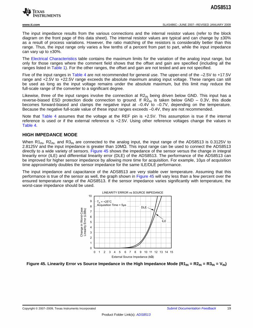
When R1IN, R2IN, and R3IN are connected to the analog input, the input range of the ADS8513 is 0.3125V to2.8125V and the input impedance is greater than 10MΩ. This input range can be used to connect the ADS8513directly to a wide variety of sensors. Figure 45 shows the impedance of the sensor versus the change in integrallinearity error (ILE) and differential linearity error (DLE) of the ADS8513. The performance of the ADS8513 canbe improved for higher sensor impedance by allowing more time for acquisition. For example, 10µs of acquisitiontime approximately doubles the sensor impedance for the same ILE/DLE performance.
The input impedance and capacitance of the ADS8513 are very stable over temperature. Assuming that thisperformance is true of the sensor as well, the graph shown in Figure 45 will vary less than a few percent over theensured temperature range of the ADS8513. If the sensor impedance varies significantly with temperature, theworst-case impedance should be used.
Figure 45. Linearity Error vs Source Impedance in the High Impedance Mode (R1IN = R2IN = R3IN = VIN)
Copyright © 2007–2009, Texas Instruments Incorporated Submit Documentation Feedback 19
Product Folder Link(s): ADS8513

DRIVING THE ADS8513 ANALOG INPUT
ADS8513
SLAS486C–JUNE 2007–REVISED JANUARY 2009 ...................................................................................................................................................... www.ti.com
In general, any reasonably fast, high-quality operational or instrumentation amplifier can be used to drive theADS8513 input. When the converter enters the acquisition mode, there is some charge injection from theconverter input to the amplifier output. This charge injection can result in inadequate settling time with sloweramplifiers. Be very careful with single-supply amplifiers, particularly if the output is required to swing very close tothe supply rails.
In addition, be careful with regard to the amplifier linearity. The outputs of single-supply and rail-to-rail amplifierscan saturate as the outputs approach the supply rails. Rather than the amplifier transfer function being a straightline, the curve can become severely S-shaped. Also, watch for the point where the amplifier switches fromsourcing current to sinking current. For some amplifiers, the transfer function can be noticeably discontinuous atthis point, causing a significant change in the output voltage for a much smaller change on the input.
Texas Instruments manufactures a wide variety of operational and instrumentation amplifiers that can be used todrive the input of the ADS8513; these devices include the OPA627, OPA132, and INA110.
20 Submit Documentation Feedback Copyright © 2007–2009, Texas Instruments Incorporated
Product Folder Link(s): ADS8513

REFERENCE
The ADS8513 can be operated with its internal 2.5V reference or an external reference. By applying an external
REF
CAP
BUF
ADS8513
www.ti.com ...................................................................................................................................................... SLAS486C–JUNE 2007–REVISED JANUARY 2009
reference voltage to the REF pin, the internal reference voltage is overdriven. The voltage at the REF input isinternally buffered by a unity gain buffer. The output of this buffer is present at the BUF and CAP pins.
The REF pin is the output of the internal 2.5V reference or the input for an external reference. A 1µF to 2.2µFtantalum capacitor should be connected between this pin and ground. The capacitor should be placed as closeto the ADS8513 as possible.
When using the internal reference, the REF pin should not be connected to any type of significant load. Anexternal load causes a voltage drop across the internal 4kΩ resistor that is in series with the internal reference.Even a 40MΩ external load to ground causes a decrease in the full-scale range of the converter by 6LSBs.
The range for the external reference is 2.3V to 2.7V. The voltage on REF determines the full-scale range of theconverter and the corresponding LSB size. Increasing the reference voltage increases the LSB size in relation tothe internal noise sources which, in turn, can improve signal-to-noise ratio. Likewise, decreasing the referencevoltage reduces the LSB size and signal-to-noise ratio.
The ADS8513 is factory-tested with 2.2µF capacitors connected to pin 6 (CAP) and pin 7 (REF). Each capacitorshould be placed as close as possible to its pin. The capacitor on pin 7 band-limits the internal reference noise.A lower-value capacitor can be used, but it may degrade SNR and SINAD. The capacitor on pin 6 stabilizes thereference buffer and provides a switching charge to the CDAC during conversion. Capacitors smaller than 1µFcan cause the buffer to become unstable and may not hold sufficient charge for the CDAC. The parts are testedto specifications with 2.2µF, so larger capacitors are not necessary. The equivalent series resistance (ESR) ofthese compensation capacitors is also critical. The total ESR must be kept under 3Ω. See the TypicalCharacteristics section concerning how ESR affects performance.
The voltage on the BUF pin is the output of the internal reference buffer. This pin is used to provide +2.5V to theanalog input or inputs for the various input configurations. The BUF output can provide up to 1mA of current toan external load. The load should be constant because variable load could affect the conversion result bymodulating the BUF voltage. Also note that the BUF output shows significant glitches as each bit decision ismade during a conversion. Between conversions, the BUF output is quiet.
Copyright © 2007–2009, Texas Instruments Incorporated Submit Documentation Feedback 21
Product Folder Link(s): ADS8513
POWER DOWN
POWER-DOWN TO POWER-UP RESPONSE
Power-Down Duration (ms)
Pow
er-
Up
Tim
e to R
ate
dA
ccura
cy (
µs) 300
250
200
150
100
50
0
0.1 1 10 100
TA = +25°C
VS
PWRD
BUSY
CS
CONV
EXT/INT
DATA
DATACLK
R1IN
GND
R2IN
R3IN
BUF
CAP
REF
GND
1
2
3
4
5
6
7
8
16
15
14
13
12
11
10
9
1
2
3
4
8
7
6
5
0.01µF1µF
1RF7604
+
Power-Down Signal
ADS8513
SLAS486C–JUNE 2007–REVISED JANUARY 2009 ...................................................................................................................................................... www.ti.com
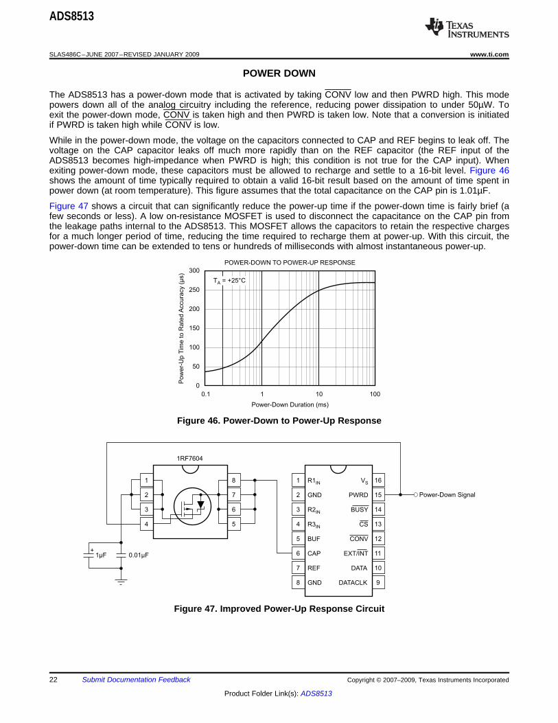
The ADS8513 has a power-down mode that is activated by taking CONV low and then PWRD high. This modepowers down all of the analog circuitry including the reference, reducing power dissipation to under 50µW. Toexit the power-down mode, CONV is taken high and then PWRD is taken low. Note that a conversion is initiatedif PWRD is taken high while CONV is low.
While in the power-down mode, the voltage on the capacitors connected to CAP and REF begins to leak off. Thevoltage on the CAP capacitor leaks off much more rapidly than on the REF capacitor (the REF input of theADS8513 becomes high-impedance when PWRD is high; this condition is not true for the CAP input). Whenexiting power-down mode, these capacitors must be allowed to recharge and settle to a 16-bit level. Figure 46shows the amount of time typically required to obtain a valid 16-bit result based on the amount of time spent inpower down (at room temperature). This figure assumes that the total capacitance on the CAP pin is 1.01µF.
Figure 47 shows a circuit that can significantly reduce the power-up time if the power-down time is fairly brief (afew seconds or less). A low on-resistance MOSFET is used to disconnect the capacitance on the CAP pin fromthe leakage paths internal to the ADS8513. This MOSFET allows the capacitors to retain the respective chargesfor a much longer period of time, reducing the time required to recharge them at power-up. With this circuit, thepower-down time can be extended to tens or hundreds of milliseconds with almost instantaneous power-up.
Figure 46. Power-Down to Power-Up Response
Figure 47. Improved Power-Up Response Circuit
22 Submit Documentation Feedback Copyright © 2007–2009, Texas Instruments Incorporated
Product Folder Link(s): ADS8513

LAYOUT
POWER FOR TSSOP-20 PACKAGE
GROUNDING
SIGNAL CONDITIONING
SENSITIVITY TO EXTERNAL DIGITAL SIGNALS
ADS8513
www.ti.com ...................................................................................................................................................... SLAS486C–JUNE 2007–REVISED JANUARY 2009
For optimum performance, tie the analog and digital power pins to the same +5V power supply and tie theanalog and digital grounds together. As noted in the Electrical Characteristics table, the ADS8513 uses 90% ofits power for the analog circuitry. The ADS8513 should be considered as an analog component.
The +5V power for the A/D converter should be separate from the +5V used for the system digital logic.Connecting +VBD directly to a digital supply can reduce converter performance because of switching noise fromthe digital logic. For best performance, the +5V supply can be produced from whatever analog supply is used forthe rest of the analog signal conditioning. If +12V or +15V supplies are present, a simple +5V regulator can beused. Although it is not suggested, if the digital supply must be used to power the converter, be sure to properlyfilter the supply. Either using a filtered digital supply or a regulated analog supply, both +VBD and +VA should betied to the same +5V source.
All of the ground pins of the A/D converter should be tied to an analog ground plane, separated from the systemdigital logic ground to achieve optimum performance. Both analog and digital ground planes should be tied to thesystem ground as close to the power supplies as possible. This layout helps to prevent dynamic digital groundcurrents from modulating the analog ground through a common impedance to power ground.
The FET switches used for the sample-and-hold on many CMOS A/D converters release a significant amount ofcharge injection that can cause the driving op amp to oscillate. The amount of charge injection that results fromthe sampling FET switch on the ADS8513 is approximately 5% to 10% of the amount on similar A/D converterswith the charge redistribution digital-to-analog converter (DAC) CDAC architecture. There is also a resistivefront-end that attenuates any charge which is released. The end result is a minimal requirement for the drivecapability on the signal conditioning preceding the A/D converter. Any op amp sufficient for the signal in anapplication is sufficient to drive the ADS8513.
The resistive front-end of the ADS8513 also provides a specified ±25V overvoltage protection. In most cases,this architecture eliminates the need for external over-voltage protection circuitry.
All successive approximation register-based A/D converters are sensitive to external noise sources. For theADS8513 and similar A/D converters, this noise most often originates because of the transition of external digitalsignals. While digital signals that run near the converter can be the source of the noise, the biggest problemoccurs with the digital inputs to the converter itself.
In many cases, the system designer may not be aware that there is a problem or the potential for a problem. Fora 12-bit system, these problems typically occur at the least significant bits and only at certain places in theconverter transfer function. For a 16-bit converter, the problem can be much easier to spot.
For example, the timing diagram in Figure 36 shows that the CONV signal should return high sometime duringtime t2. In fact, the CONV signal can return high at any time during the conversion. However, after time t2, thetransition of the CONV signal has the potential of creating a good deal of noise on the ADS8513 die. If thistransition occurs at just precisely the wrong time, the conversion results could be affected. In a similar manner,transitions on the DATACLK input could affect the conversion result.
For the ADS8513, there are 16 separate bit decisions that are made during the conversion. The most significantbit decision is made first, proceeding to the least significant bit at the end of the conversion. Each bit decisioninvolves the assumption that the bit being tested should be set. This action is combined with the result that hasbeen achieved so far. The converter compares this combined result with the actual input voltage. If the combinedresult is too high, the bit is cleared. If the result is equal to or lower than the actual input voltage, the bit remainshigh. This effect is why the basic architecture is referred to as a successive approximation register (SAR).
Copyright © 2007–2009, Texas Instruments Incorporated Submit Documentation Feedback 23
Product Folder Link(s): ADS8513
1
t
Converter
Full-Scale
Input Voltage
Range
0000
Conversion Clock
Incorrect Result
Correct Result
Actual Input
Voltage
Internal DAC
Voltage
Wrong Bit Decision Made Here
Proper SAR Operation
SAR Operation after
Wrong Bit Decision
1
(1 1)0110
External Noise
Conversion Start
(Hold Mode)
ADS8513
SLAS486C–JUNE 2007–REVISED JANUARY 2009 ...................................................................................................................................................... www.ti.com
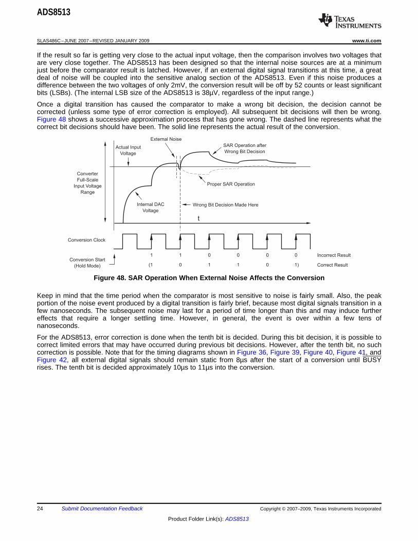
If the result so far is getting very close to the actual input voltage, then the comparison involves two voltages thatare very close together. The ADS8513 has been designed so that the internal noise sources are at a minimumjust before the comparator result is latched. However, if an external digital signal transitions at this time, a greatdeal of noise will be coupled into the sensitive analog section of the ADS8513. Even if this noise produces adifference between the two voltages of only 2mV, the conversion result will be off by 52 counts or least significantbits (LSBs). (The internal LSB size of the ADS8513 is 38µV, regardless of the input range.)
Once a digital transition has caused the comparator to make a wrong bit decision, the decision cannot becorrected (unless some type of error correction is employed). All subsequent bit decisions will then be wrong.Figure 48 shows a successive approximation process that has gone wrong. The dashed line represents what thecorrect bit decisions should have been. The solid line represents the actual result of the conversion.
Figure 48. SAR Operation When External Noise Affects the Conversion
Keep in mind that the time period when the comparator is most sensitive to noise is fairly small. Also, the peakportion of the noise event produced by a digital transition is fairly brief, because most digital signals transition in afew nanoseconds. The subsequent noise may last for a period of time longer than this and may induce furthereffects that require a longer settling time. However, in general, the event is over within a few tens ofnanoseconds.
For the ADS8513, error correction is done when the tenth bit is decided. During this bit decision, it is possible tocorrect limited errors that may have occurred during previous bit decisions. However, after the tenth bit, no suchcorrection is possible. Note that for the timing diagrams shown in Figure 36, Figure 39, Figure 40, Figure 41, andFigure 42, all external digital signals should remain static from 8µs after the start of a conversion until BUSYrises. The tenth bit is decided approximately 10µs to 11µs into the conversion.
24 Submit Documentation Feedback Copyright © 2007–2009, Texas Instruments Incorporated
Product Folder Link(s): ADS8513
APPLICATION INFORMATION
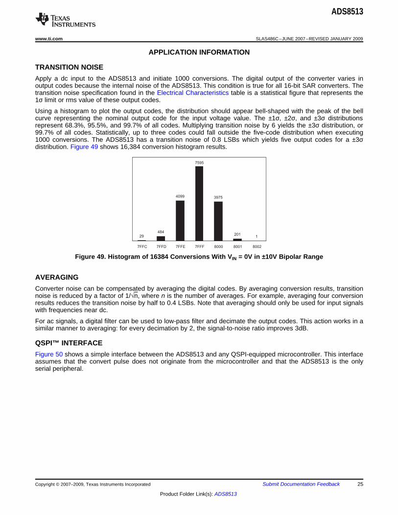
TRANSITION NOISE
29
484
4099
7595
3975
2011
7FFC 7FFD 7FFE 7FFF 8000 8001 8002
AVERAGING
QSPI™ INTERFACE
ADS8513
www.ti.com ...................................................................................................................................................... SLAS486C–JUNE 2007–REVISED JANUARY 2009
Apply a dc input to the ADS8513 and initiate 1000 conversions. The digital output of the converter varies inoutput codes because the internal noise of the ADS8513. This condition is true for all 16-bit SAR converters. Thetransition noise specification found in the Electrical Characteristics table is a statistical figure that represents the1σ limit or rms value of these output codes.
Using a histogram to plot the output codes, the distribution should appear bell-shaped with the peak of the bellcurve representing the nominal output code for the input voltage value. The ±1σ, ±2σ, and ±3σ distributionsrepresent 68.3%, 95.5%, and 99.7% of all codes. Multiplying transition noise by 6 yields the ±3σ distribution, or99.7% of all codes. Statistically, up to three codes could fall outside the five-code distribution when executing1000 conversions. The ADS8513 has a transition noise of 0.8 LSBs which yields five output codes for a ±3σdistribution. Figure 49 shows 16,384 conversion histogram results.
Figure 49. Histogram of 16384 Conversions With VIN = 0V in ±10V Bipolar Range
Converter noise can be compensated by averaging the digital codes. By averaging conversion results, transitionnoise is reduced by a factor of 1/√n, where n is the number of averages. For example, averaging four conversionresults reduces the transition noise by half to 0.4 LSBs. Note that averaging should only be used for input signalswith frequencies near dc.
For ac signals, a digital filter can be used to low-pass filter and decimate the output codes. This action works in asimilar manner to averaging: for every decimation by 2, the signal-to-noise ratio improves 3dB.
Figure 50 shows a simple interface between the ADS8513 and any QSPI-equipped microcontroller. This interfaceassumes that the convert pulse does not originate from the microcontroller and that the ADS8513 is the onlyserial peripheral.
Copyright © 2007–2009, Texas Instruments Incorporated Submit Documentation Feedback 25
Product Folder Link(s): ADS8513
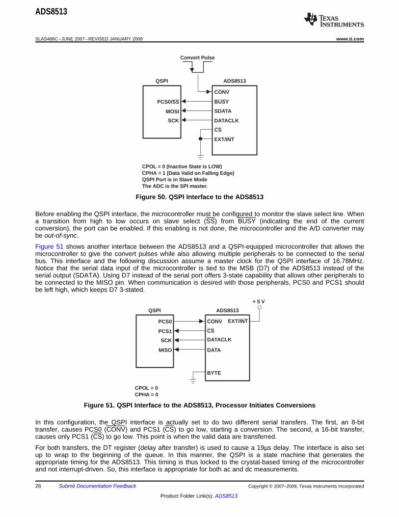
BUSY
SDATA
DATACLK
CS
EXT/INT
PCS0/SS
MOSI
SCK
QSPI ADS8513
Convert Pulse
CPOL = 0 (Inactive State is LOW)CPHA = 1 (Data Valid on Falling Edge)QSPI Port is in Slave ModeThe ADC is the SPI master.
CONV
DATA
DATACLK
CS
BYTE
PCS0
PCS1
SCK
QSPI ADS8513
CPOL = 0CPHA = 0
+ 5 V
EXT/INT
MISO
CONV
ADS8513
SLAS486C–JUNE 2007–REVISED JANUARY 2009 ...................................................................................................................................................... www.ti.com
Figure 50. QSPI Interface to the ADS8513
Before enabling the QSPI interface, the microcontroller must be configured to monitor the slave select line. Whena transition from high to low occurs on slave select (SS) from BUSY (indicating the end of the currentconversion), the port can be enabled. If this enabling is not done, the microcontroller and the A/D converter maybe out-of-sync.
Figure 51 shows another interface between the ADS8513 and a QSPI-equipped microcontroller that allows themicrocontroller to give the convert pulses while also allowing multiple peripherals to be connected to the serialbus. This interface and the following discussion assume a master clock for the QSPI interface of 16.78MHz.Notice that the serial data input of the microcontroller is tied to the MSB (D7) of the ADS8513 instead of theserial output (SDATA). Using D7 instead of the serial port offers 3-state capability that allows other peripherals tobe connected to the MISO pin. When communication is desired with those peripherals, PCS0 and PCS1 shouldbe left high, which keeps D7 3-stated.
Figure 51. QSPI Interface to the ADS8513, Processor Initiates Conversions
In this configuration, the QSPI interface is actually set to do two different serial transfers. The first, an 8-bittransfer, causes PCS0 (CONV) and PCS1 (CS) to go low, starting a conversion. The second, a 16-bit transfer,causes only PCS1 (CS) to go low. This point is when the valid data are transferred.
For both transfers, the DT register (delay after transfer) is used to cause a 19µs delay. The interface is also setup to wrap to the beginning of the queue. In this manner, the QSPI is a state machine that generates theappropriate timing for the ADS8513. This timing is thus locked to the crystal-based timing of the microcontrollerand not interrupt-driven. So, this interface is appropriate for both ac and dc measurements.
26 Submit Documentation Feedback Copyright © 2007–2009, Texas Instruments Incorporated
Product Folder Link(s): ADS8513

SPI INTERFACE
ADS8513
www.ti.com ...................................................................................................................................................... SLAS486C–JUNE 2007–REVISED JANUARY 2009
For the fastest conversion rate, the baud rate should be set to 2 (4.19MHz SCK), DT set to 10, the first serialtransfer set to 8 bits, the second set to 16 bits, and DSCK disabled (in the command control byte). This allows fora 23kSPS maximum conversion rate. For slower rates, DT should be increased. Do not slow SCK as this mayincrease the chance of affecting the conversion results or accidently initiating a second conversion during the first8-bit transfer.
In addition, CPOL and CPHA should be set to zero (SCK normally low and data captured on the rising edge).The command control byte for the 8-bit transfer should be set to 20h and for the 16-bit transfer to 61h.
The SPI interface is generally only capable of 8-bit data transfers. For some microcontrollers with SPI interfaces,it might be possible to receive data in a similar manner as shown for the QSPI interface in Figure 50. Themicrocontroller must fetch the eight most significant bits before the contents are overwritten by the leastsignificant bits.
A modified version of the QSPI interface shown in Figure 51 might be possible. For most microcontrollers with aSPI interface, the automatic generation of the start-of-conversion pulse is impossible and has to be done withsoftware. This configuration limits the interface to dc applications because of the insufficient jitter performance ofthe convert pulse itself.
Copyright © 2007–2009, Texas Instruments Incorporated Submit Documentation Feedback 27
Product Folder Link(s): ADS8513
ADS8513
SLAS486C–JUNE 2007–REVISED JANUARY 2009 ...................................................................................................................................................... www.ti.com
Revision HistoryNOTE: Page numbers for previous revisions may differ from page numbers in the current version.
Changes from Revision B (August 2008) to Revision C ................................................................................................ Page
• Changed note 4 at the bottom of the Electrical Characteristics table.................................................................................... 3
Changes from Revision A (March 2008) to Revision B .................................................................................................. Page
• Changed feature bullet for max power dissipation from 32.5W to 32.5mW .......................................................................... 1• Changed feature bullet for SPI serial port from 10Mhz to 20Mhz ......................................................................................... 1• Changed Absolute Maximum Ratings to show actual device voltage and ground................................................................ 2• Changed Electrical Characteristics to show actual device voltage and ground .................................................................... 2
28 Submit Documentation Feedback Copyright © 2007–2009, Texas Instruments Incorporated
Product Folder Link(s): ADS8513
PACKAGE OPTION ADDENDUM
www.ti.com 10-Jun-2014
Addendum-Page 1
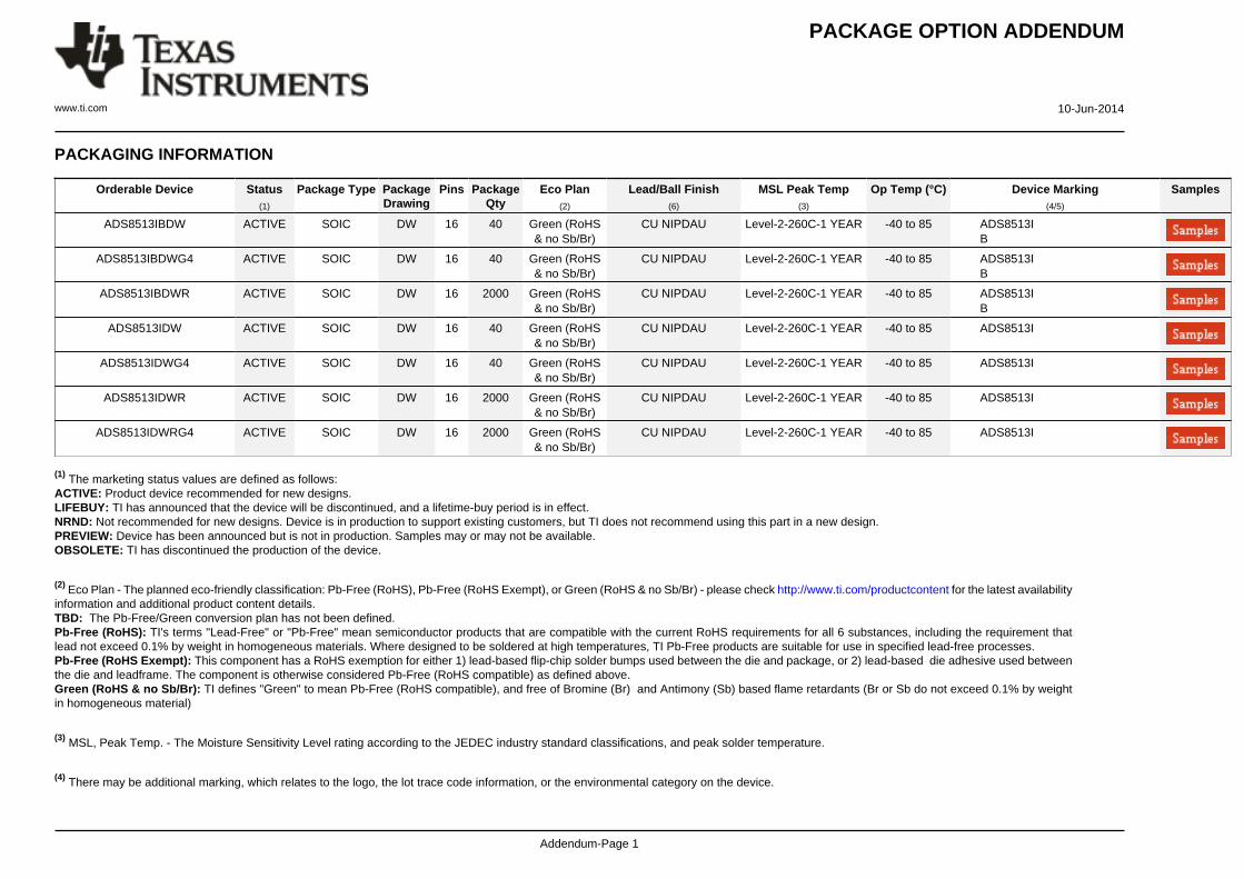
PACKAGING INFORMATION
Orderable Device Status(1)
Package Type PackageDrawing
Pins PackageQty
Eco Plan(2)
Lead/Ball Finish(6)
MSL Peak Temp(3)
Op Temp (°C) Device Marking(4/5)
Samples
ADS8513IBDW ACTIVE SOIC DW 16 40 Green (RoHS& no Sb/Br)
CU NIPDAU Level-2-260C-1 YEAR -40 to 85 ADS8513IB
ADS8513IBDWG4 ACTIVE SOIC DW 16 40 Green (RoHS& no Sb/Br)
CU NIPDAU Level-2-260C-1 YEAR -40 to 85 ADS8513IB
ADS8513IBDWR ACTIVE SOIC DW 16 2000 Green (RoHS& no Sb/Br)
CU NIPDAU Level-2-260C-1 YEAR -40 to 85 ADS8513IB
ADS8513IDW ACTIVE SOIC DW 16 40 Green (RoHS& no Sb/Br)
CU NIPDAU Level-2-260C-1 YEAR -40 to 85 ADS8513I
ADS8513IDWG4 ACTIVE SOIC DW 16 40 Green (RoHS& no Sb/Br)
CU NIPDAU Level-2-260C-1 YEAR -40 to 85 ADS8513I
ADS8513IDWR ACTIVE SOIC DW 16 2000 Green (RoHS& no Sb/Br)
CU NIPDAU Level-2-260C-1 YEAR -40 to 85 ADS8513I
ADS8513IDWRG4 ACTIVE SOIC DW 16 2000 Green (RoHS& no Sb/Br)
CU NIPDAU Level-2-260C-1 YEAR -40 to 85 ADS8513I
(1) The marketing status values are defined as follows:ACTIVE: Product device recommended for new designs.LIFEBUY: TI has announced that the device will be discontinued, and a lifetime-buy period is in effect.NRND: Not recommended for new designs. Device is in production to support existing customers, but TI does not recommend using this part in a new design.PREVIEW: Device has been announced but is not in production. Samples may or may not be available.OBSOLETE: TI has discontinued the production of the device.
(2) Eco Plan - The planned eco-friendly classification: Pb-Free (RoHS), Pb-Free (RoHS Exempt), or Green (RoHS & no Sb/Br) - please check http://www.ti.com/productcontent for the latest availabilityinformation and additional product content details.TBD: The Pb-Free/Green conversion plan has not been defined.Pb-Free (RoHS): TI's terms "Lead-Free" or "Pb-Free" mean semiconductor products that are compatible with the current RoHS requirements for all 6 substances, including the requirement thatlead not exceed 0.1% by weight in homogeneous materials. Where designed to be soldered at high temperatures, TI Pb-Free products are suitable for use in specified lead-free processes.Pb-Free (RoHS Exempt): This component has a RoHS exemption for either 1) lead-based flip-chip solder bumps used between the die and package, or 2) lead-based die adhesive used betweenthe die and leadframe. The component is otherwise considered Pb-Free (RoHS compatible) as defined above.Green (RoHS & no Sb/Br): TI defines "Green" to mean Pb-Free (RoHS compatible), and free of Bromine (Br) and Antimony (Sb) based flame retardants (Br or Sb do not exceed 0.1% by weightin homogeneous material)
(3) MSL, Peak Temp. - The Moisture Sensitivity Level rating according to the JEDEC industry standard classifications, and peak solder temperature.
(4) There may be additional marking, which relates to the logo, the lot trace code information, or the environmental category on the device.

PACKAGE OPTION ADDENDUM
www.ti.com 10-Jun-2014
Addendum-Page 2
(5) Multiple Device Markings will be inside parentheses. Only one Device Marking contained in parentheses and separated by a "~" will appear on a device. If a line is indented then it is a continuationof the previous line and the two combined represent the entire Device Marking for that device.
(6) Lead/Ball Finish - Orderable Devices may have multiple material finish options. Finish options are separated by a vertical ruled line. Lead/Ball Finish values may wrap to two lines if the finishvalue exceeds the maximum column width.
Important Information and Disclaimer:The information provided on this page represents TI's knowledge and belief as of the date that it is provided. TI bases its knowledge and belief on informationprovided by third parties, and makes no representation or warranty as to the accuracy of such information. Efforts are underway to better integrate information from third parties. TI has taken andcontinues to take reasonable steps to provide representative and accurate information but may not have conducted destructive testing or chemical analysis on incoming materials and chemicals.TI and TI suppliers consider certain information to be proprietary, and thus CAS numbers and other limited information may not be available for release.
In no event shall TI's liability arising out of such information exceed the total purchase price of the TI part(s) at issue in this document sold by TI to Customer on an annual basis.
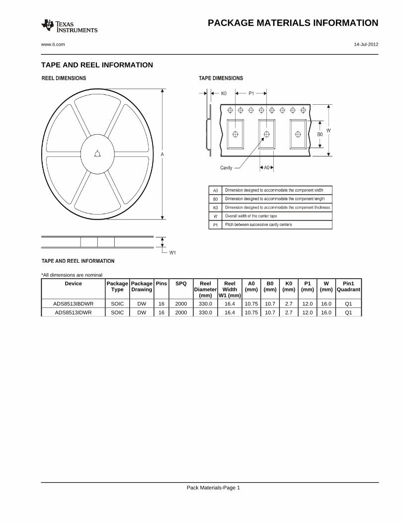
TAPE AND REEL INFORMATION
*All dimensions are nominal
Device PackageType
PackageDrawing
Pins SPQ ReelDiameter
(mm)
ReelWidth
W1 (mm)
A0(mm)
B0(mm)
K0(mm)
P1(mm)
W(mm)
Pin1Quadrant
ADS8513IBDWR SOIC DW 16 2000 330.0 16.4 10.75 10.7 2.7 12.0 16.0 Q1
ADS8513IDWR SOIC DW 16 2000 330.0 16.4 10.75 10.7 2.7 12.0 16.0 Q1
PACKAGE MATERIALS INFORMATION
www.ti.com 14-Jul-2012
Pack Materials-Page 1

*All dimensions are nominal
Device Package Type Package Drawing Pins SPQ Length (mm) Width (mm) Height (mm)
ADS8513IBDWR SOIC DW 16 2000 367.0 367.0 38.0
ADS8513IDWR SOIC DW 16 2000 367.0 367.0 38.0
PACKAGE MATERIALS INFORMATION
www.ti.com 14-Jul-2012
Pack Materials-Page 2
GENERIC PACKAGE VIEW
Images above are just a representation of the package family, actual package may vary.Refer to the product data sheet for package details.
DW 16 SOIC - 2.65 mm max heightSMALL OUTLINE INTEGRATED CIRCUIT
4040000-2/H

www.ti.com
PACKAGE OUTLINE
C
TYP10.639.97
2.65 MAX
14X 1.27
16X 0.510.31
2X8.89
TYP0.330.10
0 - 80.30.1
(1.4)
0.25GAGE PLANE
1.270.40
A
NOTE 3
10.510.1
BNOTE 4
7.67.4
4220721/A 07/2016
SOIC - 2.65 mm max heightDW0016ASOIC
NOTES: 1. All linear dimensions are in millimeters. Dimensions in parenthesis are for reference only. Dimensioning and tolerancing per ASME Y14.5M. 2. This drawing is subject to change without notice. 3. This dimension does not include mold flash, protrusions, or gate burrs. Mold flash, protrusions, or gate burrs shall not exceed 0.15 mm, per side. 4. This dimension does not include interlead flash. Interlead flash shall not exceed 0.25 mm, per side.5. Reference JEDEC registration MS-013.
1 16
0.25 C A B
98
PIN 1 IDAREA
SEATING PLANE
0.1 C
SEE DETAIL A
DETAIL ATYPICAL
SCALE 1.500

www.ti.com
EXAMPLE BOARD LAYOUT
0.07 MAXALL AROUND
0.07 MINALL AROUND
(9.3)
14X (1.27)
R0.05 TYP
16X (2)
16X (0.6)
4220721/A 07/2016
SOIC - 2.65 mm max heightDW0016ASOIC
NOTES: (continued) 6. Publication IPC-7351 may have alternate designs. 7. Solder mask tolerances between and around signal pads can vary based on board fabrication site.
METAL SOLDER MASKOPENING
NON SOLDER MASKDEFINED
SOLDER MASK DETAILS
OPENINGSOLDER MASK METAL
SOLDER MASKDEFINED
LAND PATTERN EXAMPLESCALE:7X
SYMM
1
8 9
16
SEEDETAILS
SYMM

www.ti.com
EXAMPLE STENCIL DESIGN
R0.05 TYP
16X (2)
16X (0.6)
14X (1.27)
(9.3)
4220721/A 07/2016
SOIC - 2.65 mm max heightDW0016ASOIC
NOTES: (continued) 8. Laser cutting apertures with trapezoidal walls and rounded corners may offer better paste release. IPC-7525 may have alternate design recommendations. 9. Board assembly site may have different recommendations for stencil design.
SOLDER PASTE EXAMPLEBASED ON 0.125 mm THICK STENCIL
SCALE:7X
SYMM
SYMM
1
8 9
16

IMPORTANT NOTICE
Texas Instruments Incorporated (TI) reserves the right to make corrections, enhancements, improvements and other changes to itssemiconductor products and services per JESD46, latest issue, and to discontinue any product or service per JESD48, latest issue. Buyersshould obtain the latest relevant information before placing orders and should verify that such information is current and complete.TI’s published terms of sale for semiconductor products (http://www.ti.com/sc/docs/stdterms.htm) apply to the sale of packaged integratedcircuit products that TI has qualified and released to market. Additional terms may apply to the use or sale of other types of TI products andservices.Reproduction of significant portions of TI information in TI data sheets is permissible only if reproduction is without alteration and isaccompanied by all associated warranties, conditions, limitations, and notices. TI is not responsible or liable for such reproduceddocumentation. Information of third parties may be subject to additional restrictions. Resale of TI products or services with statementsdifferent from or beyond the parameters stated by TI for that product or service voids all express and any implied warranties for theassociated TI product or service and is an unfair and deceptive business practice. TI is not responsible or liable for any such statements.Buyers and others who are developing systems that incorporate TI products (collectively, “Designers”) understand and agree that Designersremain responsible for using their independent analysis, evaluation and judgment in designing their applications and that Designers havefull and exclusive responsibility to assure the safety of Designers' applications and compliance of their applications (and of all TI productsused in or for Designers’ applications) with all applicable regulations, laws and other applicable requirements. Designer represents that, withrespect to their applications, Designer has all the necessary expertise to create and implement safeguards that (1) anticipate dangerousconsequences of failures, (2) monitor failures and their consequences, and (3) lessen the likelihood of failures that might cause harm andtake appropriate actions. Designer agrees that prior to using or distributing any applications that include TI products, Designer willthoroughly test such applications and the functionality of such TI products as used in such applications.TI’s provision of technical, application or other design advice, quality characterization, reliability data or other services or information,including, but not limited to, reference designs and materials relating to evaluation modules, (collectively, “TI Resources”) are intended toassist designers who are developing applications that incorporate TI products; by downloading, accessing or using TI Resources in anyway, Designer (individually or, if Designer is acting on behalf of a company, Designer’s company) agrees to use any particular TI Resourcesolely for this purpose and subject to the terms of this Notice.TI’s provision of TI Resources does not expand or otherwise alter TI’s applicable published warranties or warranty disclaimers for TIproducts, and no additional obligations or liabilities arise from TI providing such TI Resources. TI reserves the right to make corrections,enhancements, improvements and other changes to its TI Resources. TI has not conducted any testing other than that specificallydescribed in the published documentation for a particular TI Resource.Designer is authorized to use, copy and modify any individual TI Resource only in connection with the development of applications thatinclude the TI product(s) identified in such TI Resource. NO OTHER LICENSE, EXPRESS OR IMPLIED, BY ESTOPPEL OR OTHERWISETO ANY OTHER TI INTELLECTUAL PROPERTY RIGHT, AND NO LICENSE TO ANY TECHNOLOGY OR INTELLECTUAL PROPERTYRIGHT OF TI OR ANY THIRD PARTY IS GRANTED HEREIN, including but not limited to any patent right, copyright, mask work right, orother intellectual property right relating to any combination, machine, or process in which TI products or services are used. Informationregarding or referencing third-party products or services does not constitute a license to use such products or services, or a warranty orendorsement thereof. Use of TI Resources may require a license from a third party under the patents or other intellectual property of thethird party, or a license from TI under the patents or other intellectual property of TI.TI RESOURCES ARE PROVIDED “AS IS” AND WITH ALL FAULTS. TI DISCLAIMS ALL OTHER WARRANTIES ORREPRESENTATIONS, EXPRESS OR IMPLIED, REGARDING RESOURCES OR USE THEREOF, INCLUDING BUT NOT LIMITED TOACCURACY OR COMPLETENESS, TITLE, ANY EPIDEMIC FAILURE WARRANTY AND ANY IMPLIED WARRANTIES OFMERCHANTABILITY, FITNESS FOR A PARTICULAR PURPOSE, AND NON-INFRINGEMENT OF ANY THIRD PARTY INTELLECTUALPROPERTY RIGHTS. TI SHALL NOT BE LIABLE FOR AND SHALL NOT DEFEND OR INDEMNIFY DESIGNER AGAINST ANY CLAIM,INCLUDING BUT NOT LIMITED TO ANY INFRINGEMENT CLAIM THAT RELATES TO OR IS BASED ON ANY COMBINATION OFPRODUCTS EVEN IF DESCRIBED IN TI RESOURCES OR OTHERWISE. IN NO EVENT SHALL TI BE LIABLE FOR ANY ACTUAL,DIRECT, SPECIAL, COLLATERAL, INDIRECT, PUNITIVE, INCIDENTAL, CONSEQUENTIAL OR EXEMPLARY DAMAGES INCONNECTION WITH OR ARISING OUT OF TI RESOURCES OR USE THEREOF, AND REGARDLESS OF WHETHER TI HAS BEENADVISED OF THE POSSIBILITY OF SUCH DAMAGES.Unless TI has explicitly designated an individual product as meeting the requirements of a particular industry standard (e.g., ISO/TS 16949and ISO 26262), TI is not responsible for any failure to meet such industry standard requirements.Where TI specifically promotes products as facilitating functional safety or as compliant with industry functional safety standards, suchproducts are intended to help enable customers to design and create their own applications that meet applicable functional safety standardsand requirements. Using products in an application does not by itself establish any safety features in the application. Designers mustensure compliance with safety-related requirements and standards applicable to their applications. Designer may not use any TI products inlife-critical medical equipment unless authorized officers of the parties have executed a special contract specifically governing such use.Life-critical medical equipment is medical equipment where failure of such equipment would cause serious bodily injury or death (e.g., lifesupport, pacemakers, defibrillators, heart pumps, neurostimulators, and implantables). Such equipment includes, without limitation, allmedical devices identified by the U.S. Food and Drug Administration as Class III devices and equivalent classifications outside the U.S.TI may expressly designate certain products as completing a particular qualification (e.g., Q100, Military Grade, or Enhanced Product).Designers agree that it has the necessary expertise to select the product with the appropriate qualification designation for their applicationsand that proper product selection is at Designers’ own risk. Designers are solely responsible for compliance with all legal and regulatoryrequirements in connection with such selection.Designer will fully indemnify TI and its representatives against any damages, costs, losses, and/or liabilities arising out of Designer’s non-compliance with the terms and provisions of this Notice.
Mailing Address: Texas Instruments, Post Office Box 655303, Dallas, Texas 75265Copyright © 2018, Texas Instruments Incorporated