16-bit, 625 msps, 2x interpolating, dual-channel digital … 100 pattern test de-interleave 8 sample...
TRANSCRIPT

100
100
Pa
ttern
Test
De-i
nte
rle
ave
8S
am
ple
FIF
O16
16
100
x
sin(x)
x
sin(x)
x2
x2
Coa
rse
Mix
er
Fs/4
,-F
s/4
,F
s/2
Pro
gra
mm
able
De
lay
(0-1
5T
)
1.2 V
Reference
16-b
DAC
16-b
DAC
Control InterfaceTemp
Sensor
Clock Distribution
A
gain
B
gainFrame Strobe
EXTIO
BIASJ
IOUTA1
IOUTA2
IOUTB1
IOUTB2
DACCLKP
DACCLKN
DATACLKP
DATACLKN
D7P
D7N
D0P
D0N
FRAMEP
FRAMEN
OSTRP
OSTRN
A
offset
B
offset
AL
AR
M_
SD
O
SD
IO
SD
EN
B
SC
LK
TX
EN
AB
LE
RE
SE
TB
AVDD33
CL
KV
DD
18
DIG
VD
D1
8
VF
US
E
DA
CV
DD
18
GN
D
LVPECL
LVDS
LVPECL
LVDS
LVDS
FIR0FIR4
5 taps 59 taps
100
LVDS
Product
Folder
Sample &Buy
Technical
Documents
Tools &
Software
Support &Community
DAC3282SLAS646C –DECEMBER 2009–REVISED MAY 2015
DAC3282 16-Bit, 625 MSPS, 2x Interpolating, Dual-Channel Digital-to-Analog Converter(DAC)
1 Features 3 DescriptionThe DAC3282 is a dual-channel 16-bit 625 MSPS
1• Dual, 16-Bit, 625 MSPS DACsdigital-to-analog converter (DAC) with an 8-bit LVDS• 8-Bit Input LVDS Data Bus input data bus with on-chip termination, optional 2x
– Byte-Wide Interleaved Data Load interpolation filter, and internal voltage reference. TheDAC3282 offers superior linearity, noise and crosstalk– 8 Sample Input FIFOperformance.– Optional Data Pattern CheckerInput data can be interpolated by 2x through an on-• Multi-DAC Synchronizationchip interpolating FIR filter with over 85 dB of stop-• Optional 2x Interpolation Filter band attenuation. Multiple DAC3282 devices can be
• Zero-IF Sinc Correction Filter fully synchronized.• Fs/2 and ± Fs/4 Coarse Mixer The DAC3282 allows either a complex or real output.• Digital Offset Adjustment for LO Correction An optional coarse mixer in complex mode provides
frequency upconversion and the dual DAC output• Temperature Sensorproduces a complex Hilbert Transform pair. The• 3- or 4-Wire Serial Control Interface digital offset correction feature allows optimization of
• On Chip 1.2-V reference LO feed-through of an external quadrature modulatorperforming the final single sideband RF up-• Differential Scalable Output: 2 to 20 mAconversion.• Low Power: 950 mW at 625 MSPS, 845 mW at
500 MHz, Full Operating Conditions The DAC3282 is characterized for operation over theentire industrial temperature range of –40°C to 85°C• Space Saving Package: 48-pin 7×7mm VQFNand is available in a 48-pin 7×7mm VQFN package.
2 ApplicationsDevice Information(1)
• Cellular Base Stations PART NUMBER PACKAGE BODY SIZE (NOM)• Diversity Transmit DAC3282 VQFN (48) 7.00 mm × 7.00 mm• Wideband Communications (1) For all available packages, see the orderable addendum at
the end of the data sheet.• Digital Synthesis
Simplified Schematic
1
An IMPORTANT NOTICE at the end of this data sheet addresses availability, warranty, changes, use in safety-critical applications,intellectual property matters and other important disclaimers. PRODUCTION DATA.

DAC3282SLAS646C –DECEMBER 2009–REVISED MAY 2015 www.ti.com
Table of Contents7.4 Device Functional Modes........................................ 271 Features .................................................................. 17.5 Programming .......................................................... 302 Applications ........................................................... 17.6 Register Maps ........................................................ 323 Description ............................................................. 1
8 Application and Implementation ........................ 454 Revision History..................................................... 28.1 Application Information............................................ 455 Pin Configuration and Functions ......................... 48.2 Typical Application ................................................. 516 Specifications......................................................... 6
9 Power Supply Recommendations ...................... 536.1 Absolute Maximum Ratings ...................................... 69.1 Power-up Sequence................................................ 536.2 ESD Ratings ............................................................ 6
10 Layout................................................................... 546.3 Recommended Operating Conditions....................... 610.1 Layout Guidelines ................................................. 546.4 Thermal Information ................................................. 710.2 Layout Example .................................................... 556.5 Electrical Characteristics – DC Specifications ......... 7
11 Device and Documentation Support ................. 566.6 Electrical Characteristics – AC Specifications .......... 911.1 Device Support...................................................... 566.7 Electrical Characteristics – Digital Specifications ... 1011.2 Community Resources.......................................... 576.8 Timing Characteristics ........................................... 1111.3 Trademarks ........................................................... 576.9 Typical Characteristics ............................................ 1211.4 Electrostatic Discharge Caution............................ 577 Detailed Description ............................................ 1611.5 Glossary ................................................................ 577.1 Overview ................................................................. 16
12 Mechanical, Packaging, and Orderable7.2 Functional Block Diagram ....................................... 16Information ........................................................... 577.3 Feature Description................................................. 16
4 Revision History
Changes from Revision B (May 2012) to Revision C Page
• Changed data sheet global format to include Device Information and ESD Rating tables, Feature Descriptionsection, Device Functional Modes, Application and Implementation section, Power Supply Recommendationssection, Layout section, Device and Documentation Support section, and Mechanical, Packaging, and OrderableInformation section ................................................................................................................................................................ 1
• Added design parameters for application example .............................................................................................................. 51
Changes from Revision A (February 2010) to Revision B Page
• Added to Description of the PIN FUNCTIONS table pin no.31, FROM: Bi-directional in 3-pin....(default). TO: Bi-directional in 3-pin....(default) and 4-pin mode. ..................................................................................................................... 5
• Changed FIFO block diagram Figure 24 ............................................................................................................................. 17• Added 4th & 5th paragraphs to the INPUT FIFO section, under Figure 24. ........................................................................ 17• Changed Figure 25 .............................................................................................................................................................. 18• Added "CONFIG19 multi_sync_sel" to FIFO MODES OF OPERATION section ................................................................ 19• Changed Mode descriptions in FIFO Operation Modes, Table 1, from "Enabled" to "Single Sync Source" and added
new FIFO Mode, "Dual Sync Sources"................................................................................................................................. 19• Changed the "DATA PATTERN CHECKER" section text for clarification............................................................................ 19• Changed from "SDIO is data in only" to "SDIO is bidirectional" in SERIAL INTERFACE section first paragraph, ............. 30• Changed FROM: "In 4 pin.....cycle(s)." TO: "In 4 pin configuration, both ALARM_SDO and SDIO are data out from
DAC3282." in paragraph under Figure 32.. .......................................................................................................................... 31• Changed Bit 5 function to: Allows the FRAME input to reset the FIFO write pointer when asserted. AND changed Bit
4 first sentence to: "Allows the FRAME or OSTR signal to reset the FIFO read pointer when asserted." in CONFIG0Register description ............................................................................................................................................................. 33
• Changed CONFIG3 Register table from: "CONFIG1, 0x01 to CONFIG3, 0x03" and in Bit 4:2 Function From: "Whenthe FIFO......read pointer." TO: "This is the default FIFO read pointer position after the FIFO read pointer has beensynchronized." ..................................................................................................................................................................... 34
• Changed CONFIG7 register table, BIt 6 Function description "This alarm indicates......more detail."................................. 36
2 Submit Documentation Feedback Copyright © 2009–2015, Texas Instruments Incorporated
Product Folder Links: DAC3282

DAC3282www.ti.com SLAS646C –DECEMBER 2009–REVISED MAY 2015
• Added text string to CONFIG18 Register table, Bit 1 Function description for clarification. ................................................ 39• Moved the MULTI-DEVICE SYNCHRONIZATION section to follow "Bypass Mode" section.............................................. 45• Changed the illustration for Figure 74. ................................................................................................................................. 45• Changed the illustration for Figure 76 ................................................................................................................................. 47• Changed the POWER-UP-SEQUENCE section for clarification. ......................................................................................... 53• Deleted SNR definition and added: Noise Spectral....Nyquist zone. ................................................................................... 56
Changes from Original (December 2009) to Revision A Page
• Deleted FIFO_OSTRP and FIFO_OSTRN descriptions from Pin Functions table. N/A for this device. ................................ 5• Changed Default from 0x41 to 0x43 for Register name VERSION31 in Table 8 Register Map.......................................... 32• Changed Default address from 0x41 to 0x43 for Register name:VERSION31; and Default Value for Bit 5:0 from
000001 to 000011................................................................................................................................................................. 44
Copyright © 2009–2015, Texas Instruments Incorporated Submit Documentation Feedback 3
Product Folder Links: DAC3282

37
38
39
40
41
42
43
44
45
46
47
48
1
2
3
4
5
6
7
8
9
10
11
122
4
23
22
21
20
19
18
17
16
15
14
13
35
34
33
32
31
30
29
28
27
26
25
DAC3282
RGZ Package
48-QFN 7x7mm
(Top View)
36
GND
DACCLKN
D5
P
D5
N
D4
P
D4
N
DA
TA
CL
KP
DA
TA
CL
KN
FR
AM
EP
FR
AM
EN
D3
P
D3
N
D2
P
D2
ND1P
D1N
D0P
D0N
TXENABLE
SDIO
SCLK
SDENB
AV
DD
33
AV
DD
33
IOU
TB
1
IOU
TB
2
VF
US
E
BIA
SJ
EX
TIO
AV
DD
33
IOU
TA
2
IOU
TA
1
AV
DD
33
AV
DD
33
D6N
D6P
D7N
D7P
DIGVDD18
OSTRN
OSTRP
DACCLKP
DACVDD18
CLKVDD18 RESETB
DACVDD18
ALARM_SDO
DIGVDD18
DAC3282SLAS646C –DECEMBER 2009–REVISED MAY 2015 www.ti.com
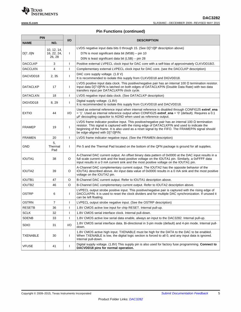
5 Pin Configuration and Functions
RGZ Package48-Pin VQFN with Thermal Pad
Top View
Pin FunctionsPIN
I/O DESCRIPTIONNAME NO.
37, 40, 42,AVDD33 I Analog supply voltage. (3.3 V)45, 481.8V CMOS output for ALARM condition. The ALARM output functionality is defined through theCONFIG6 register. Default polarity is active low, but can be changed to active high via CONFIG0ALARM_SDO 34 O alarm_pol control bit. Optionally, it can be used as the uni-directional data output in 4-pin serialinterface mode (CONFIG 23 sif4_ena = ‘1’).
BIASJ 43 O Full-scale output current bias. For 20mA full-scale output current, connect a 960 Ω resistor to GND.Internal clock buffer supply voltage. (1.8 V)CLKVDD18 1 I It is recommended to isolate this supply from DACVDD18 and DIGVDD18.LVDS positive input data bits 0 through 7. Each positive/negative LVDS pair has an internal 100 Ωtermination resistor. Data format relative to DATACLKP/N clock is Double Data Rate (DDR) with twodata transfers per DATACKP/N clock cycle. Dual channel 16-bit data is transferred byte-wide on this
9, 11, 13, single 8-bit data bus using FRAMEP/N as a frame strobe indicator.D[7..0]P 15, 21, 23, I
D7P is most significant data bit (MSB) – pin 925, 27D0P is least significant data bit (LSB) – pin 27
The order of the bus can be reversed via CONFIG19 rev bit.
4 Submit Documentation Feedback Copyright © 2009–2015, Texas Instruments Incorporated
Product Folder Links: DAC3282
DAC3282www.ti.com SLAS646C –DECEMBER 2009–REVISED MAY 2015
Pin Functions (continued)PIN
I/O DESCRIPTIONNAME NO.
LVDS negative input data bits 0 through 15. (See D[7:0]P description above)10, 12, 14,D[7..0]N 16, 22, 24, I D7N is most significant data bit (MSB) – pin 10
26, 28 D0N is least significant data bit (LSB) – pin 28DACCLKP 3 I Positive external LVPECL clock input for DAC core with a self-bias of approximately CLKVDD18/2.DACCLKN 4 I Complementary external LVPECL clock input for DAC core. (see the DACCLKP description)
DAC core supply voltage. (1.8 V)DACVDD18 2, 35 I It is recommended to isolate this supply from CLKVDD18 and DIGVDD18.LVDS positive input data clock. This positive/negative pair has an internal 100 Ω termination resistor.
DATACLKP 17 I Input data D[7:0]P/N is latched on both edges of DATACLKP/N (Double Data Rate) with two datatransfers input per DATACLKP/N clock cycle.
DATACLKN 18 I LVDS negative input data clock. (See DATACLKP description)Digital supply voltage. (1.8V)DIGVDD18 8, 29 I It is recommended to isolate this supply from CLKVDD18 and DACVDD18.Used as external reference input when internal reference is disabled through CONFIG25 extref_ena
EXTIO 44 I/O = ‘1’. Used as internal reference output when CONFIG25 extref_ena = ‘0’ (default). Requires a 0.1μF decoupling capacitor to AGND when used as reference output.LVDS frame indicator positive input. This positive/negative pair has an internal 100 Ω terminationresistor. This signal is captured with the rising edge of DATACLKP/N and used to indicate theFRAMEP 19 I beginning of the frame. It is also used as a reset signal by the FIFO. The FRAMEP/N signal shouldbe edge-aligned with D[7:0]P/N.
FRAMEN 20 I LVDS frame indicator negative input. (See the FRAMEN description)5,
GND Thermal I Pin 5 and the Thermal Pad located on the bottom of the QFN package is ground for all supplies.Pad
A-Channel DAC current output. An offset binary data pattern of 0x0000 at the DAC input results in aIOUTA1 38 O full scale current sink and the least positive voltage on the IOUTA1 pin. Similarly, a 0xFFFF data
input results in a 0 mA current sink and the most positive voltage on the IOUTA1 pin.A-Channel DAC complementary current output. The IOUTA2 has the opposite behavior of the
IOUTA2 39 O IOUTA1 described above. An input data value of 0x0000 results in a 0 mA sink and the most positivevoltage on the IOUTA2 pin.
IOUTB1 47 O B-Channel DAC current output. Refer to IOUTA1 description above.IOUTB2 46 O B-Channel DAC complementary current output. Refer to IOUTA2 description above.
LVPECL output strobe positive input. This positive/negative pair is captured with the rising edge ofOSTRP 6 I DACCLKP/N. It is used to reset the clock dividers and for multiple DAC synchronization. If unused it
can be left floating.OSTRN 7 I LVPECL output strobe negative input. (See the OSTRP description)RESETB 36 I 1.8V CMOS active low input for chip RESET. Internal pull-up.SCLK 32 I 1.8V CMOS serial interface clock. Internal pull-down.SDENB 33 I 1.8V CMOS active low serial data enable, always an input to the DAC3282. Internal pull-up.
1.8V CMOS serial interface data. Bi-directional in 3-pin mode (default) and 4-pin mode. Internal pull-SDIO 31 I/O down.1.8V CMOS active high input. TXENABLE must be high for the DATA to the DAC to be enabled.
TXENABLE 30 I When TXENABLE is low, the digital logic section is forced to all 0, and any input data is ignored.Internal pull-down.Digital supply voltage. (1.8V) This supply pin is also used for factory fuse programming. Connect toVFUSE 41 I DACVDD18 pins for normal operation.
Copyright © 2009–2015, Texas Instruments Incorporated Submit Documentation Feedback 5
Product Folder Links: DAC3282

DAC3282SLAS646C –DECEMBER 2009–REVISED MAY 2015 www.ti.com
6 Specifications
6.1 Absolute Maximum Ratingsover operating free-air temperature range (unless otherwise noted) (1)
MIN MAX UNITDACVDD18 (2) –0.5 2.3DIGVDD18 (2) –0.5 2.3
Supply CLKVDD18 (2) –0.5 2.3 VvoltageVFUSE (2) –0.5 2.3AVDD33 (2) –0.5 4CLKVDD18 to DIGVDD18 –0.5 0.5DACVDD18 to DIGVDD18 –0.5 0.5D[7..0]P ,D[7..0]N, DATACLKP,DATACLKN, FRAMEP, FRAMEN (2) –0.5 DIGVDD18 + 0.5
Terminal DACCLKP, DACCLKN, OSTRP, OSTRN (2) –0.5 CLKVDD18 + 0.5 VvoltageALARM_SDO, SDIO, SCLK, SDENB, RESETB, TXENABLE (2) –0.5 DIGVDD18 + 0.5IOUTA1/B1, IOUTA2/B2 (2) –1.0 AVDD33 + 0.5EXTIO, BIASJ (2) –0.5 AVDD33 + 0.5
Peak input current (any input) 20 mAPeak total input current (all inputs) –30 mATA Operating free-air temperature, DAC3282 –40 85 °CTstg Storage temperature –65 150 °C
(1) Stresses beyond those listed under Absolute Maximum Ratings may cause permanent damage to the device. These are stress ratingsonly, which do not imply functional operation of the device at these or any other conditions beyond those indicated under RecommendedOperating Conditions. Exposure to absolute-maximum-rated conditions for extended periods may affect device reliability.
(2) Measured with respect to GND.
6.2 ESD RatingsVALUE UNIT
Human-body model (HBM), per ANSI/ESDA/JEDEC JS-001 (1) ±2000V(ESD) Electrostatic discharge VCharged-device model (CDM), per JEDEC specification JESD22- ±500C101 (2)
(1) JEDEC document JEP155 states that 500-V HBM allows safe manufacturing with a standard ESD control process.(2) JEDEC document JEP157 states that 250-V CDM allows safe manufacturing with a standard ESD control process.
6.3 Recommended Operating Conditionsover operating free-air temperature range (unless otherwise noted)
MIN NOM MAX UNIT1.8-V DAC core supply voltage, DACDVDD18 1.7 1.8 1.9 V1.8-V digital supply voltage, DIGVDD18 1.7 1.8 1.9 V
Voltage1.8-V internal clock buffer supply voltage, CLKVDD18 1.7 1.8 1.9 V3.3-V analog supply voltage, AVDD33 3.0 3.3 3.6 V
6 Submit Documentation Feedback Copyright © 2009–2015, Texas Instruments Incorporated
Product Folder Links: DAC3282

DAC3282www.ti.com SLAS646C –DECEMBER 2009–REVISED MAY 2015
6.4 Thermal InformationDAC3282
THERMAL METRIC (1) RGZ (VQFN) UNIT48 PINS
RθJA Junction-to-ambient thermal resistance 26.3 °C/WRθJC(top) Junction-to-case (top) thermal resistance 12.2 °C/WRθJB Junction-to-board thermal resistance 3.7 °C/WψJT Junction-to-top characterization parameter 0.2 °C/WψJB Junction-to-board characterization parameter 3.6 °C/WRθJC(bot) Junction-to-case (bottom) thermal resistance 0.7 °C/W
(1) For more information about traditional and new thermal metrics, see the Semiconductor and IC Package Thermal Metrics applicationreport, SPRA953.
6.5 Electrical Characteristics – DC Specifications (1)
over recommended operating free-air temperature range, nominal supplies, IOUTFS = 20 mA (unless otherwise noted)PARAMETER TEST CONDITIONS MIN TYP MAX UNIT
Resolution 16 BitsDC ACCURACYDNL Differential nonlinearity ±2 LSB
1 LSB = IOUTFS/216INL Integral nonlinearity ±4 LSBANALOG OUTPUT
Coarse gain linearity ±0.04 LSBOffset error Mid code offset 0.01 %FSR
With external reference ±2 %FSRGain error
With internal reference ±2 %FSRGain mismatch With internal reference –2 2 %FSRMinimum full scale output current 2Nominal full-scale current, IOUTFS = mA16 × IBIAS current.Maximum full scale output current 20
AVDD AVDDOutput compliance range (2) IOUTFS = 20 mA V–0.5V +0.5VOutput resistance 300 kΩOutput capacitance 5 pF
REFERENCE OUTPUTVREF Reference output voltage 1.14 1.2 1.26 V
Reference output current (3) 100 nAREFERENCE INPUTVEXTIO Input voltage range 0.1 1.2 1.25 V
External Reference ModeInput resistance 1 MΩSmall signal bandwidth 472 kHzInput capacitance 100 pF
TEMPERATURE COEFFICIENTSppm ofOffset drift ±1 FSR/°C
With external reference ±15 ppm ofGain drift FSR/°CWith internal reference ±30Reference voltage drift ±8 ppm/°C
(1) Measured differential across IOUTA1 and IOUTA2 or IOUTB1 and IOUTB2 with 25 Ω each to AVDD.(2) The lower limit of the output compliance is determined by the CMOS process. Exceeding this limit may result in transistor breakdown,
resulting in reduced reliability of the DAC3282 device. The upper limit of the output compliance is determined by the load resistors andfull-scale output current. Exceeding the upper limit adversely affects distortion performance and integral nonlinearity.
(3) Use an external buffer amplifier with high impedance input to drive any external load.
Copyright © 2009–2015, Texas Instruments Incorporated Submit Documentation Feedback 7
Product Folder Links: DAC3282

DAC3282SLAS646C –DECEMBER 2009–REVISED MAY 2015 www.ti.com
Electrical Characteristics – DC Specifications(1) (continued)over recommended operating free-air temperature range, nominal supplies, IOUTFS = 20 mA (unless otherwise noted)
PARAMETER TEST CONDITIONS MIN TYP MAX UNITPOWER SUPPLY
AVDD33 3.0 3.3 3.6 VDACVDD18, DIGVDD18, 1.7 1.8 1.9 VCLKVDD18
I(AVDD33) Analog supply current 96 mAI(DIGVDD18) Digital supply current 268 mA
Mode 1(below)I(DACVDD18) DAC supply current 74 mAI(CLKVDD18) Clock supply current 10 mA
Power down mode analog supplyI(AVDD33) 2 mAcurrentPower down mode digital supplyI(DIGVDD18) 3 mAcurrent
Mode 4 (below)Power down mode DAC supplyI(DACVDD18) 0.5 mAcurrentPower down mode clock supplyI(CLKVDD18) 1 mAcurrent
Mode 1: fDAC = 625MSPS, 2xinterpolation, mixer on, 950 1100 mWDigital Offset Control onMode 2: fDAC = 491.52MSPS, 2xinterpolation, Zero-IF 845 mWCorrection Filter on, mixer off, DigitalOffset Control onMode 3: Sleep Mode, fDAC =625MSPS, 2X interpolation, mixer
P Power Dissipation on, 575 mWDAC in sleep mode:CONFIG24 sleepa, sleepb set to 1Mode 4: Power-Down mode, Noclock, static data pattern, DAC inpower-down mode:
15 mWCONFIG23 clkpath_sleep_a,clkpath_sleepb set to 1CONFIG24 clkrecv_sleep, sleepa,sleepb set to 1
PSRR Power Supply Rejection Ratio DC tested –0.4 0.4 %/FSR/VT Operating Range –40 25 85 °C
8 Submit Documentation Feedback Copyright © 2009–2015, Texas Instruments Incorporated
Product Folder Links: DAC3282

DAC3282www.ti.com SLAS646C –DECEMBER 2009–REVISED MAY 2015
6.6 Electrical Characteristics – AC Specificationsover recommended operating free-air temperature range, nominal supplies, IOUTFS = 20 mA (unless otherwise noted)
PARAMETER TEST CONDITIONS MIN TYP MAX UNITANALOG OUTPUT (1)
1x Interpolation 312.5fDAC Maximum output update rate MSPS
2x Interpolation 625No interpolation, FIFO off, Offset off, 38Inverse sinc off2x Interpolation 59 DAC clockDigital Latency Zero-IF Sinc Correction Filter 16 cyclesFIFO 8Offset 4
AC PERFORMANCE (2)
fDAC = 625 MSPS, fOUT = 10.1 MHz 832x Interp, DAC A+B onSpurious Free Dynamic Range fDAC = 625 MSPS, fOUT = 20.1 MHzSFDR 78 dBcSFDR (0 to fDAC/2) Tone at 0 dBFS 2x Interp, DAC A+B on
fDAC = 625 MSPS, fOUT = 70.1 MHz 642x Interp, DAC A+B onfDAC = 625 MSPS, fOUT = 30 ± 0.5 82MHz 2x Interp, DAC A+B on
Third-order two-tone intermodulation fDAC = 625 MSPS, fOUT = 50 ± 0.5IMD3 80 dBcdistortion Each tone at –6 dBFS MHz 2x Interp, DAC A+B onfDAC = 625 MSPS, fOUT = 150 ± 0.5 69MHz 2x Interp, DAC A+B on,fDAC = 625 MSPS, fOUT = 10.1 MHz 1612x Interp, DAC A+B onNoise Spectral Density Single ToneNSD dBc/Hzat 0 dBm fDAC = 625 MSPS, fOUT = 150.1 MHz 1502x Interp, DAC A+B onfDAC = 491.52 MSPS, fOUT= 30.72 81MHz 2x Interp, DAC A+B onAdjacent Channel Leakage Ratio, dBcSingle Carrier fDAC = 491.52 MSPS, fOUT = 153.6 76MHz 2x Interp, DAC A+B on
WCDMA (3)fDAC = 491.52 MSPS, fOUT = 30.72 84 dBcMHz 2x Interp, DAC A+B onAlternate Channel Leakage Ratio,
Single Carrier fDAC = 491.52 MSPS, fOUT = 153.6 77 dBcMHz 2x Interp, DAC A+B onChannel Isolation fDAC = 625 MSPS, fOUT = 10 MHz 84 dBc
(1) Measured single ended into 50 Ω load.(2) 4:1 transformer output termination, 50 Ω doubly terminated load.(3) Single carrier, W-CDMA with 3.84 MHz BW, 5-MHz spacing, centered at IF, PAR = 12dB. TESTMODEL 1, 10 ms
Copyright © 2009–2015, Texas Instruments Incorporated Submit Documentation Feedback 9
Product Folder Links: DAC3282
DAC3282SLAS646C –DECEMBER 2009–REVISED MAY 2015 www.ti.com
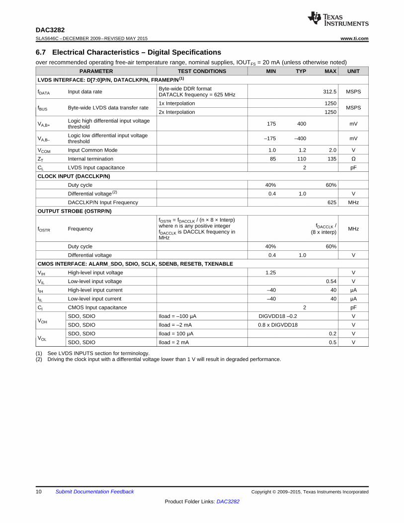
6.7 Electrical Characteristics – Digital Specificationsover recommended operating free-air temperature range, nominal supplies, IOUTFS = 20 mA (unless otherwise noted)
PARAMETER TEST CONDITIONS MIN TYP MAX UNITLVDS INTERFACE: D[7:0]P/N, DATACLKP/N, FRAMEP/N (1)
Byte-wide DDR formatfDATA Input data rate 312.5 MSPSDATACLK frequency = 625 MHz1x Interpolation 1250
fBUS Byte-wide LVDS data transfer rate MSPS2x Interpolation 1250
Logic high differential input voltageVA,B+ 175 400 mVthresholdLogic low differential input voltageVA,B– –175 –400 mVthreshold
VCOM Input Common Mode 1.0 1.2 2.0 VZT Internal termination 85 110 135 ΩCL LVDS Input capacitance 2 pFCLOCK INPUT (DACCLKP/N)
Duty cycle 40% 60%Differential voltage (2) 0.4 1.0 VDACCLKP/N Input Frequency 625 MHz
OUTPUT STROBE (OSTRP/N)fOSTR = fDACCLK / (n × 8 × Interp)
fDACCLK /where n is any positive integerfOSTR Frequency MHzfDACCLK is DACCLK frequency in (8 x interp)MHz
Duty cycle 40% 60%Differential voltage 0.4 1.0 V
CMOS INTERFACE: ALARM_SDO, SDIO, SCLK, SDENB, RESETB, TXENABLEVIH High-level input voltage 1.25 VVIL Low-level input voltage 0.54 VIIH High-level input current –40 40 μAIIL Low-level input current –40 40 μACI CMOS Input capacitance 2 pF
SDO, SDIO Iload = –100 μA DIGVDD18 –0.2 VVOH SDO, SDIO Iload = –2 mA 0.8 x DIGVDD18 V
SDO, SDIO Iload = 100 μA 0.2 VVOL SDO, SDIO Iload = 2 mA 0.5 V
(1) See LVDS INPUTS section for terminology.(2) Driving the clock input with a differential voltage lower than 1 V will result in degraded performance.
10 Submit Documentation Feedback Copyright © 2009–2015, Texas Instruments Incorporated
Product Folder Links: DAC3282

DAC3282www.ti.com SLAS646C –DECEMBER 2009–REVISED MAY 2015
6.8 Timing Characteristicsover recommended operating free-air temperature range, nominal supplies, IOUTFS = 20 mA (unless otherwise noted)
PARAMETER TEST CONDITIONS MIN TYP MAX UNITANALOG OUTPUT (1)
ts(DAC) Output settling time to 0.1% Transition: Code 0x0000 to 0xFFFF 10.4 nsDAC outputs are updated on the
tpd Output propagation delay falling edge of DAC clock. Does not 2 nsinclude Digital Latency (see below).
tr(IOUT) Output rise time 10% to 90% 220 pstf(IOUT) Output fall time 90% to 10% 220 PS
IOUT current settling to 1% ofIOUTFS. Measured from SDENBDAC Wake-up Time 90 μsrising edge; Register CONFIG24,toggle sleepa from 1 to 0
Power-upIOUT current settling to less thantime1% of IOUTFS. Measured from
DAC Sleep Time SDENB rising edge; Register 90 μsCONFIG24, toggle sleepa from 0 to1.
TIMING LVDS INPUTS: DATACLKP/N, double edge latching – See Figure 25Setup time, D[7:0]P/N and FRAMEP/N latched on rising edgets(DATA) FRAMEP/N, valid to either edge of 0 psof DATACLKP/N onlyDATACLKP/NHold time, D[7:0]P/N and FRAMEP/N latched on rising edgeth(DATA) FRAMEP/N, valid after either edge 400 psof DATACLKP/N onlyof DATACLKP/N
fDATACLK is DATACLK frequency in 1/2fDATACLt(FRAME) FRAMEP/N pulse width nsMHz K
Maximum offset between FIFO Bypass Mode only 1/2fDACCLKt_align DATACLKP/N and DACCLKP/N fDACCLK is DACCLK frequency in ns–0.55rising edges MHzTIMING OSTRP/N Input: DACCLKP/N rising edge latching
Setup time, OSTRP/N valid to risingts(OSTR) 200 psedge of DACCLKP/NHold time, OSTRP/N valid afterth(OSTR) 200 psrising edge of DACCLKP/N
SERIAL PORT TIMING – See Figure 40 and Figure 41Setup time, SDENB to rising edge ofts(SDENB) 20 nsSCLKSetup time, SDIO valid to risingts(SDIO) 10 nsedge of SCLKHold time, SDIO valid to rising edgeth(SDIO) 5 nsof SCLK
Register CONFIG5 read 1 μs(temperature sensor read)t(SCLK) Period of SCLKAll other registers 100 nsRegister CONFIG5 read 0.4 μs(temperature sensor read)t(SCLKH) High time of SCLKAll other registers 40 nsRegister CONFIG5 read 0.4 μs(temperature sensor read)t(SCLKL) Low time of SCLKAll other registers 40 ns
Data output delay after falling edgetd(Data) 10 nsof SCLKtRESET Minimum RESETB pulsewidth 25 ns
(1) Measured single ended into 50 Ω load.
Copyright © 2009–2015, Texas Instruments Incorporated Submit Documentation Feedback 11
Product Folder Links: DAC3282

50
55
60
65
70
75
80
f = 200 MSPSDAC
f = 600 MSPSDAC
f = 400 MSPSDAC
SF
DR
- S
pu
rio
us F
ree D
yn
am
ic R
an
ge -
dB
c
0 50 100 150 200 250fOUT - Output Frequency - MHz
2x interpolation, 0 dBFS,IOUTS = 20 mA
20 mA
10 mA
2 mA
50
55
60
65
70
75
80
85
90
SF
DR
- S
pu
rio
us F
ree D
yn
am
ic R
an
ge -
dB
c
0 50 100 150 200 250fOUT - Output Frequency - MHz
f = 625 MSPS, 2x interpolation,
0 dBFSDAC
0 20 40 60 80 100 120
1x Interpolation
2x Interpolation
f = 312.5 MSPS, 0 dBFS,
IOUTFS = 20 mADAC
50
55
60
65
70
75
80
85
90
SF
DR
- S
pu
rio
us F
ree D
yn
am
ic R
an
ge -
dB
c
fOUT - Output Frequency - MHz
50
55
60
65
70
75
80
85
90
0 50 100 150 200 250
0 dBFS
-6 dBFS
-12 dBFS
SF
DR
- S
pu
rio
us F
ree D
yn
am
ic R
an
ge -
dB
c
f - Output Frequency - MHzOUT
f = 625 MSPS, 2x Interpolation,
IOUTFS = 20 mADAC
-5
-4
-3
-2
-1
0
1
2
3
4
5
Erro
r -
LS
B
0 10000 20000 30000 40000 50000 60000 70000
Code
DNL
0 10000 20000 30000 40000 50000 60000 70000
Code
-5
-4
-3
-2
-1
0
1
2
3
4
5
Erro
r -
LS
B
INL
DAC3282SLAS646C –DECEMBER 2009–REVISED MAY 2015 www.ti.com
6.9 Typical Characteristics
Figure 1. Integral Non-Linearity Figure 2. Differential Non-Linearity
Figure 3. SFDR vs Input Scale Figure 4. SFDR vs Interpolation
Figure 5. SFDR vs fDAC Figure 6. SFDR vs IOUTFS
12 Submit Documentation Feedback Copyright © 2009–2015, Texas Instruments Incorporated
Product Folder Links: DAC3282

50
55
60
65
70
75
80
85
90
95
100
0 50 100 150 200 250
20 mA
10 mA
2 mA
f = 625 MSPS, 2x Interpolation,
Tones at f ± 0.5 MHz, 0 dBFSDAC
OUT
IMD
3 -
dB
c
fOUT - Output Frequency - MHz
50
55
60
65
70
75
80
85
90
0 50 100 150 200 250
f = 200 MSPSDAC
f = 400 MSPSDAC
f = 600 MSPSDAC
2x Interpolation,Tones at f ± 0.5 MHz,
0 dBFS, IOUTS = 20 mAOUT
fOUT - Output Frequency - MHz
IMD
3 -
dB
c
50
55
60
65
70
75
80
85
90
95
0 dBFS
-6 dBFS
-12 dBFS
0 50 100 150 200 250fOUT - Output Frequency - MHz
IMD
3 -
dB
c
f = 625 MSPS, 2x Interpolation,
Tones at f ± 0.5 MHz,
IOUTFS = 20 mA
DAC
OUT
65
70
75
80
85
90
0 20 40 60 80 100 120
1x Interpolation
2x Interpolation
fOUT - Output Frequency - MHz
IMD
3 -
dB
c
f = 312.5 MSPS,
Tones at f ± 0.5 MHz,
0 dBFS, IOUTFS = 20 mA
DAC
OUT
0 50 100 150 200 250 300f - Frequency - MHz
-90
-80
-70
-60
-50
-40
-30
-20
-10
0
10P
ow
er
- d
Bm
2x Interpolation, 0 dBFS,f = 625 MSPS,
= 10 MHzDAC
fOUT
0 50 100 150 200 250 300f - Frequency - MHz
-90
-80
-70
-60
-50
-40
-30
-20
-10
0
10
Po
wer
- d
Bm
2x Interpolation, 0 dBFS,f = 625 MSPS,
f = 100 MHzDAC
OUT
DAC3282www.ti.com SLAS646C –DECEMBER 2009–REVISED MAY 2015
Typical Characteristics (continued)
Figure 8. Single Tone Spectral PlotFigure 7. Single Tone Spectral Plot
Figure 10. IMD3 vs InterpolationFigure 9. IMD3 vs Input Scale
Figure 11. IMD3 vs fDAC Figure 12. IMD3 vs IOUTFS
Copyright © 2009–2015, Texas Instruments Incorporated Submit Documentation Feedback 13
Product Folder Links: DAC3282

55
60
65
70
75
80
ACLR, 0 dBFS
ACLR -6 dBFS
Aternate, 0 dBFS
Alternate, -6 dBFS
0 50 100 150 200 250fOUT - Output Frequency - MHz
AC
LR
- d
Bc
f = 491.52 MSPS, 2x Interpolation
IOUTFS = 20 mADAC
65
70
75
80
85
90
Adjacent 0 dBFS
Adjacent -6 dBFS
Alternate 0 dBFS
Alternate -6 dBFS
0 50 100 150 200 250fOUT - Output Frequency - MHz
AC
LR
- d
Bc
f = 491.52 MSPS, 2x Interpolation,
IOUTFS = 20 mADAC
130
135
140
145
150
155
160
165
170
f = 200 MSPSDAC
f = 400 MSPSDAC
f = 600 MSPSDAC
0 50 100 150 200 250fOUT - Output Frequency - MHz
NS
D -
dB
c/H
z
2x Interpolation, 0 dBFS,IOUTS = 20 mA
130
135
140
145
150
155
160
165
170
20 mA
10 mA
2 mA
0 50 100 150 200 250fOUT - Output Frequency - MHz
f = 625 MSPS,
2x Interpolation 0 dBFSDAC
130
135
140
145
150
155
160
165
170
0 dBFS
-6 dBFS
-12 dBFS
0 50 100 150 200 250fOUT - Output Frequency - MHz
NS
D -
dB
c/H
z
f = 625 MSPS, 2x Interpolation,
IOUTFS = 20 mADAC
140
145
150
155
160
165
170
0 20 40 60 80 100 120
1x Interpolation
2x Interpolation
fOUT - Output Frequency - MHz
NS
D -
dB
c/H
z
f = 312.5 MSPS, 0 dBFS,
IOUTFS = 20 mADAC
DAC3282SLAS646C –DECEMBER 2009–REVISED MAY 2015 www.ti.com
Typical Characteristics (continued)
Figure 13. NSD vs Input Scale Figure 14. NSD vs Interpolation
Figure 15. NSD vs fDAC Figure 16. NSD vs IOUTFS
Figure 17. Single Carrier WCDMA ACLR vs Input Scale Figure 18. Four Carrier WCDMA ACLR vs Input Scale
14 Submit Documentation Feedback Copyright © 2009–2015, Texas Instruments Incorporated
Product Folder Links: DAC3282

0
20
40
60
80
100
120
0 100 200 300 400 500 600
AV
DD
33 -
mA
f - MSPSDAC
0
10
20
30
40
50
60
70
80
90
100
0 100 200 300 400 500 600
Coarse_mix on
Coarse_mix off
DA
CV
DD
- m
A
f - MSPSDAC
0
2
4
6
8
10
12
14
16
18
20
0 100 200 300 400 500 600
CL
KV
DD
18 -
mA
f - MSPSDAC
0
50
100
150
200
250
300
1x
1x+invsinc
2x
2x+invsinc
2x+coarse_mix
0 50 100 150 200 250 300 350f - MSPSDATA
DV
DD
18 -
mA
1x
1x+invsinc
2x
2x+invsinc
2x+coarse_mix
0 50 100 150 200 250 300 350f - MSPSDATA
400
500
600
700
800
900
1000
Po
wer
- m
W
DAC3282www.ti.com SLAS646C –DECEMBER 2009–REVISED MAY 2015
Typical Characteristics (continued)
Figure 19. Power vs fDATA Figure 20. DVDD18 vs fDATA
Figure 22. CLKVDD18 vs fDACFigure 21. DACVDD18 vs fDAC
Figure 23. AVDD33 vs fDAC
Copyright © 2009–2015, Texas Instruments Incorporated Submit Documentation Feedback 15
Product Folder Links: DAC3282

100
100
Pa
ttern
Test
De-i
nte
rle
ave
8S
am
ple
FIF
O16
16
100
x
sin(x)
x
sin(x)
x2
x2
Coa
rse
Mix
er
Fs/4
,-F
s/4
,F
s/2
Pro
gra
mm
able
De
lay
(0-1
5T
)
1.2 V
Reference
16-b
DAC
16-b
DAC
Control InterfaceTemp
Sensor
Clock Distribution
A
gain
B
gainFrame Strobe
EXTIO
BIASJ
IOUTA1
IOUTA2
IOUTB1
IOUTB2
DACCLKP
DACCLKN
DATACLKP
DATACLKN
D7P
D7N
D0P
D0N
FRAMEP
FRAMEN
OSTRP
OSTRN
A
offset
B
offset
AL
AR
M_
SD
O
SD
IO
SD
EN
B
SC
LK
TX
EN
AB
LE
RE
SE
TB
AVDD33
CL
KV
DD
18
DIG
VD
D1
8
VF
US
E
DA
CV
DD
18
GN
D
LVPECL
LVDS
LVPECL
LVDS
LVDS
FIR0FIR4
5 taps 59 taps
100
LVDS
DAC3282SLAS646C –DECEMBER 2009–REVISED MAY 2015 www.ti.com
7 Detailed Description
7.1 OverviewThe DAC3282 is a dual-channel 16-bit 800 MSPS digital-to-analog converter (DAC) with an 8-bit LVDS inputdata bus with on-chip termination, optional 2x-4x interpolation filters, digital IQ compensation and internal voltagereference. Input data can be interpolated by 2x or 4x through on-chip interpolating FIR filters with over 85 dB ofstop-band attenuation. Multiple DAC3282 devices can be fully synchronized. The DAC3282 allows either acomplex or real output. An optional coarse mixer in complex mode provides frequency upconversion and the dualDAC output produces a complex Hilbert Transform pair. The digital IQ compensation feature allows optimizationof phase, gain and offset to maximize sideband rejection and minimize LO feed-through of an externalquadrature modulator performing the final single sideband RF up-conversion.
7.2 Functional Block Diagram
7.3 Feature Description
7.3.1 Input FIFOThe DAC3282 includes a 2-channel, 16-bits wide and 8-samples deep input FIFO which acts as an elastic buffer.The purpose of the FIFO is to absorb any timing variations between the input data and the internal DAC datarate clock such as the ones resulting from clock-to-data variations from the data source.
Figure 24 shows the block diagram of the FIFO.
16 Submit Documentation Feedback Copyright © 2009–2015, Texas Instruments Incorporated
Product Folder Links: DAC3282

Frame Align
0
1
2
3
4
5
6
7
FRAME
D[7:0]
0…
7
Wri
teP
oin
ter
FIFO I Output
FIFO Q Output
Clock Handoff
Input Side
Clocked by DATACLKOutput Side
Clocked by FIFO Out Clock
(DACCLK/Interpolation Factor)
FIFO:
2 x 16-bits wide
8-samples deep
0
1
2
3
4
5
6
7
Sample 0
I0 [15:0], Q0 [15:0]
Sample 2
I2 [15:0], Q2 [15:0]
Sample 3
I3 [15:0], Q3 [15:0]
Sample 4
I4 [15:0], Q4 [15:0]
Sample 5
I5 [15:0], Q5 [15:0]
Sample 6
I6 [15:0], Q6 [15:0]
Sample 7
I7 [15:0], Q7 [15:0]
Sample 1
I1 [15:0], Q1 [15:0]
Initial
Position
0…
7
Re
ad
Poin
ter
Initial
Position
32-bit 32-bit
I-data, 16-bit
Q-data, 16-bit
16-bit
16-bit
Two DATACLK cycles to capture2x 16-bit of I-data and Q-data
Data[15:8] 8-bit
Data[7:0] 8-bit
Write Pointer Reset
OSTR
fifo_offset(2:0)
multi_sync_enaS M
Read Pointer Reset
fifo_reset_ena
0
S (Single Sync Source Mode). Reset handoff from input side to output side.M (Dual Sync Sources Mode). OSTR resets read pointer. Multi-DAC synchronization
DAC3282www.ti.com SLAS646C –DECEMBER 2009–REVISED MAY 2015
Feature Description (continued)
Figure 24. DAC3282 FIFO Block Diagram
Data is written to the device 8-bits at a time on the rising and falling edges of DATACLK. In order to form acomplete 32-bit wide sample (16-bit I-data and 16-bit Q-data) two DATACLK periods are required as shown inFigure 25. Each 32-bit wide sample is written into the FIFO at the address indicated by the write pointer.Similarly, data from the FIFO is read by the FIFO Out Clock 32-bits at a time from the address indicated by theread pointer. The FIFO Out Clock is generated internally from the DACCLK signal and its rate is equal toDACCLK/Interpolation. Each time a FIFO write or FIFO read is done the corresponding pointer moves to the nextaddress.
The reset position for the FIFO read and write pointers is set by default to addresses 0 and 4 as shown inFigure 24. This offset gives optimal margin within the FIFO. The default read pointer location can be set toanother value using fifo_offset(2:0) in register CONFIG3. Under normal conditions data is written-to and read-from the FIFO at the same rate and consequently the write and read pointer gap remains constant. If the FIFOwrite and read rates are different, the corresponding pointers will be cycling at different speeds which could resultin pointer collision. Under this condition the FIFO attempts to read and write data from the same address at thesame time which will result in errors and thus must be avoided.
The FRAME signal besides acting as a frame indicator can also used to reset the FIFO pointers to their initiallocation. Unlike Data, the FRAME signal is latched only on the rising edges of DATACLK. When a rising edgeoccurs on FRAME, the pointers will return to their original position. The write pointer is always set back toposition 0 upon reset. The read pointer reset position is determined by fifo_offset (address 4 by default).
Similarly, the read pointer sync source is selected by multi_sync_sel (CONFIG19). Either the FRAME or OSTRsignal can be set to reset the read pointer. If FRAME is used to reset the read pointer, the FIFO Out Clock willrecapture the FRAME signal to reset the read pointer. This clock domain transfer (DATACLK to FIFO Out Clock)results in phase ambiguity of the reset signal. This limits the precise control of the output timing and makes fullsynchronization of multiple devices difficult.
Copyright © 2009–2015, Texas Instruments Incorporated Submit Documentation Feedback 17
Product Folder Links: DAC3282

I4[15:8] I4[7:0] Q4[15:8] Q4[7:0]Q3[7:0] I5[7:0] Q5[15:8] Q5[7:0]I5[15:8] I6[7:0] Q6[15:8]I6[15:8] Q6[7:0] I7[15:8] I7[7:0] Q7[15:8]Q3[15:8]D[7:0]P/N
LV
DS
Pa
irs
(Data
So
urc
e) Write sample 4 to FIFO (32-bits)
DATACLKP /N
(DDR)
FRAMEP/NResets write pointer to position 0
Write I4[15:8] (8-bits) to
DAC on rising edge
Write I4[7:0] (8-bits) to
DAC on falling edge
Write Q4[15:8] (8-bits) to
DAC on rising edge
Write Q4[7:0] (8-bits) to
DAC on falling edgets(DATA)
th(DATA)
ts(DATA)
th(DATA)
ts(DATA)th(DATA)
DACCLKP/N
2 x interpolation
OSTRP/N
Resets read pointer to position
ts(OSTR) th(OSTR)
(optionally internalsync from write reset)
set by fifo_offset (4 by default)
LV
PE
CL
Pa
irs
(Clo
ck S
ou
rce
)
DAC3282SLAS646C –DECEMBER 2009–REVISED MAY 2015 www.ti.com
Feature Description (continued)To alleviate this, the device offers the alternative of resetting the FIFO read pointer independently of the writepointer by using the OSTR signal. The OSTR signal is sampled by DACCLK and must satisfy the timingrequirements in the specification table. In order to minimize the skew it is recommended to use the same clockdistribution device such as Texas Instruments CDCE62005 to provide the DACCLK and OSTR signals to all theDAC3282 devices in the system. Swapping the polarity of the DACCLK output with respect to the OSTR outputestablishes proper phase relationship.
The FIFO pointers reset procedure can be done periodically or only once during initialization as the pointersautomatically return to the initial position when the FIFO has been filled. To reset the FIFO periodically, it isnecessary to have FRAME and OSTR signals to repeat at multiple of 8 FIFO samples. To disable FIFO reset, setfifo_reset_ena and multi_sync_ena (CONFIG0) to 0.
The frequency limitation for the FRAME signal is the following
fSYNC = fDATACLK/(n x 16) where n = 1, 2,...
The frequency limitation for the OSTR signal is the following:
fOSTR = fDAC/(n x interpolation x 8) where n = 1, 2, ...
The frequencies above are at maximum when n = 1. This is when FRAME and OSTR have a rising edgetransition every 8 FIFO samples. The occurrence can be made less frequent by setting n > 1, for example, everyn x 8 FIFO samples.
Figure 25. FIFO Write Description
7.3.2 FIFO AlarmsThe FIFO only operates correctly when the write and read pointers are positioned properly. If either pointer overor under runs the other, samples will be duplicated or skipped. To prevent this, register CONFIG7 can be used totrack three FIFO related alarms:• alarm_fifo_2away. Occurs when the pointers are within two addresses of each other.• alarm_fifo_1away. Occurs when the pointers are within one address of each other.• alarm_fifo_collision. Occurs when the pointers are equal to each other.
These three alarm events are generated asynchronously with respect to the clocks and can be accessed eitherthrough CONFIG7 or through the ALARM_SDO pin.
18 Submit Documentation Feedback Copyright © 2009–2015, Texas Instruments Incorporated
Product Folder Links: DAC3282

DAC3282www.ti.com SLAS646C –DECEMBER 2009–REVISED MAY 2015
Feature Description (continued)7.3.3 FIFO Modes of OperationThe DAC3282 input FIFO can be completely bypassed through registers config0 and config19. The registerconfiguration for each mode is described in Table 1.
Register Control BitsCONFIG0 fifo_ena, fifo_reset_ena, multi_sync_enaCONFIG19 multi_sync_sel
Table 1. FIFO Operation Modesconfig0 FIFO Bits Config19
FIFO Mode fifo_ena fifo_reset_ena multi_sync_ena multi_sync_selDual Sync Sources 1 1 1 0Single Sync Source 1 1 1 1Bypass 0 X X X
7.3.4 Dual Sync Sources ModeThis is the recommended mode of operation for those applications that require precise control of the outputtiming. In Dual Sync Sources mode, the FIFO write and read pointers are reset independently. The FIFO writepointer is reset using the LVDS FRAME signal, and the FIFO read pointer is reset using the LVPECL OSTRsignal. This allows LVPECL OSTR signal to control the phase of the output for either a single chip or multiplechips. Multiple devices can be fully synchronized in this mode.
7.3.5 Single Sync Source ModeIn Single Sync Source mode, the FIFO write and read pointers are reset from the same LVDS FRAME signal.This mode has a possibility of up to 2 DAC clocks offset between the outputs of multiple devices (the DACoutputs of the same device maintain the phase phase). Applications requiring exact output timing control willneed Dual Sync Sources mode instead of Single Sync Source Mode. A rising edge for FIFO and clock dividersync is recommended. Periodic sync signal is not recommended due to non-deterministic latency of the syncsignal through the clock domain transfer.
7.3.6 Bypass ModeIn FIFO bypass mode, the FIFO block is not used. As a result the input data is handed off from the DATACLK tothe DACCLK domain without any compensation. In this mode the relationship between DATACLK and DACCLKt(align) is critical and used as a synchronizing mechanism for the internal logic. Due to the t(align) constraint it ishighly recommended that a clock synchronizer such as Texas Instruments' CDCM7005 or CDCE62005 is usedto provide both clock inputs. In bypass mode the pointers have no effect on the data path or handoff.
7.3.7 Data Pattern CheckerThe DAC3282 incorporates a simple pattern checker test in order to determine errors in the data interface. Themain cause of failure is setup/hold timing issues. The test mode is enabled by asserting iotest_ena in registerconfig1. In test mode the analog outputs are deactivated regardless of the state of TXENABLE.
The data pattern key used for the test is 8 words long and is specified by the contents of iotest_pattern[0:7] inregisters config9 through config16. The data pattern key can be modified by changing the contents of theseregisters.
The first word in the test frame is determined by a rising edge transition in FRAME. At this transition, the pattern0word should be input to the data pins. Patterns 1 through 7 should follow sequentially on each edge of DATACLK(rising and falling). The sequence should be repeated until the pattern checker test is disabled by settingiotest_ena back to “0”. It is not necessary to have a rising FRAME edge aligned with every pattern0 word, justthe first one to mark the beginning of the series.
Copyright © 2009–2015, Texas Instruments Incorporated Submit Documentation Feedback 19
Product Folder Links: DAC3282

D[7:0]P/N
FRAMEP/N
DATACLKP/N (DDR)
Pattern 0[7:0]
Pattern 1[7:0]
Pattern 2[7:0]
Pattern 3[7:0]
Pattern 4[7:0]
Pattern 5[7:0]
Pattern 6[7:0]
Pattern 7[7:0]
Start cycle again with optional rising edge of FRAME
DAC3282SLAS646C –DECEMBER 2009–REVISED MAY 2015 www.ti.com
Figure 26. IO Pattern Checker Data Transmission Format
The test mode determines if the 8-bit LVDS data D[7:0]P/N of all the patterns were received correctly bycomparing the received data against the data pattern key. If any of the 8-bit data D[7:0]P/N were receivedincorrectly, the corresponding bits in iotest_results(7:0) in register config8 will be set to “1” to indicate bit errorlocation. Furthermore, the error condition will trigger the alarm_from_iotest bit in register config7 to indicate ageneral error in the data interface. When data pattern checker mode is enabled, this alarm in register config7, bit3 is the only valid alarm. Other alarms in register config7 are not valid and can be disregarded.
For instance, pattern0 is programmed to the default of 0x7A. If the received Pattern 0 is 0x7B, then bit 0 iniotest_results(7:0) will be set to “1” to indicate an error in bit 0 location. The alarm_from_iotest will also be set to“1” to report the data transfer error. The user can then narrow down the error from the bit location informationand implement the fix accordingly.
The alarms can be cleared by writing 0x00 to iotest_results(7:0) and “0” to alarm_from_iotest through the serialinterface. The serial interface will read back 0s if there are no errors or if the errors are cleared. Thecorresponding alarm bit will remain a “1” if the errors remain.
It is recommended to enable the pattern checker and then run the pattern sequence for 100 or more completecycles before clearing the iotest_results(7:0) and alarm_from_iotest. This will eliminate the possibility of falsealarms generated during the setup sequence.
20 Submit Documentation Feedback Copyright © 2009–2015, Texas Instruments Incorporated
Product Folder Links: DAC3282

Pattern
0 ... 7
D[7:0]
8-Bit
8-Bit
8-Bit
DATACLK
iotest_results[7]
iotest_results[0]
alarm_from_iotestOnly oneedge needed
FRAMELVDS
Drivers
Go back to 0 after cycle or newrising edge on FRAME
Pattern 0Bit-by-Bit Compare
Pattern 1Bit-by-Bit Compare
Pattern 2Bit-by-Bit Compare
Pattern 3Bit-by-Bit Compare
Pattern 4Bit-by-Bit Compare
Pattern 5Bit-by-Bit Compare
Pattern 6Bit-by-Bit Compare
Pattern 7Bit-by-Bit Compare
0
1
2
3
4
5
6
7
0
1
2
3
4
5
6
7
8-BitInput
8-BitInput
8-BitInput
Bit 7Results
Bit 0Results
•••
•••
•••
All BitsResults
iotest_pattern0
iotest_pattern1
iotest_pattern2
iotest_pattern3
iotest_pattern4
iotest_pattern5
iotest_pattern6
iotest_pattern7
DataFormat
DAC3282www.ti.com SLAS646C –DECEMBER 2009–REVISED MAY 2015
Figure 27. DAC3282 Pattern Check Block Diagram
Copyright © 2009–2015, Texas Instruments Incorporated Submit Documentation Feedback 21
Product Folder Links: DAC3282

0 0.05 0.1 0.15 0.2 0.25 0.3 0.35 0.4 0.45 0.5-4
-3
-2
-1
0
1
2
3
4
FIR4
Corrected
Sin(x)/x
f /fOUT DAC
Mag
nit
ud
e -
dB
0 0.02 0.04 0.06 0.08 0.1 0.12 0.14 0.16 0.18 0.2
-0.5
-0.4
-0.3
-0.2
-0.1
0
0.1
0.2
0.3
0.4
0.5
FIR4
Sin(x)/x
Corrected
Mag
nit
ud
e -
dB
f /fOUT DAC
0.36 0.37 0.38 0.39 0.4 0.41 0.42 0.43 0.44 0.45 0.46
-0.5
-0.4
-0.3
-0.2
-0.1
0
0.1
Ma
gn
itu
de
- d
B
f/fin
0 0.1 0.2 0.3 0.4 0.5 0.6 0.7 0.8 0.9 1-160
-140
-120
-100
-80
-60
-40
-20
0
20
Ma
gn
itu
de
- d
B
f/fin
DAC3282SLAS646C –DECEMBER 2009–REVISED MAY 2015 www.ti.com
7.3.8 FIR FiltersThe DAC3282 has two FIR filters, a 2x interpolation FIR (FIR0) and a non-interpolating FIR (FIR4) thatcompensates for the sinc droop of the DAC on zero-IF applications. The correction filter is placed before theinterpolating filter and can only be used with both FIRs enabled.
Figure 28 shows the magnitude spectrum response for FIR0, a 59-tap interpolating half-band filter. The transitionband is from 0.4 to 0.6 × fIN (the input data rate for the FIR filter) with < 0.002dB of pass-band ripple and > 85 dBstop-band attenuation. Figure 29 shows the transition band region from 0.36 to 0.46 × fIN. Up to 0.45 × fIN there isless than 0.5 dB of attenuation.
Figure 28. Magnitude Spectrum for FIR0 Figure 29. FIR0 Transition Band
Figure 31. Correction Range of Zero-IF SincFigure 30. Magnitude Spectrum for Zero-IF SincCorrection Filter 0 to 0.2 × fDACCorrection Filter up to 0.5 × fDAC
22 Submit Documentation Feedback Copyright © 2009–2015, Texas Instruments Incorporated
Product Folder Links: DAC3282

DAC3282www.ti.com SLAS646C –DECEMBER 2009–REVISED MAY 2015
The DAC sample and hold operation results in the well known sin(x)/x or sinc(x) frequency response shown inFigure 30 (red line). The DAC3282 has a 5-tap inverse sinc filter (FIR4) placed before the 2x interpolation filter tocompensate for this effect up to 0.2 × fDAC. The inverse sinc filter runs at the input data rate and is operationalonly if the 2x interpolation filter is enabled as well, correspondingly the rate of this filter is always half of the DACupdate rate. As a result, the filter cannot completely flatten the frequency response of the sample and hold outputas shown in Figure 30.
Figure 31 shows the magnitude spectrum for FIR4 over the correction range. The inverse sinc filter response(Figure 31, black line) has approximately the opposite frequency response to sin(x)/x between 0 to 0.2 x fDAC,resulting in the corrected response in Figure 31 (blue line). Between 0 to 0.2 × fDAC, the inverse sinc filtercompensates for the sample and hold roll-off with less than 0.04-dB error.
The filter taps for all digital filters are listed in Table 2.
Table 2. FIR Filter CoefficientsFIR4FIR0 Non-Interpolating Zero-IF2x Interpolating Half-Band Filter Sinc Correction Filter
59 Taps 5 Taps4 4 10 0 –5
–12 –12 264 (1)
0 0 –528 28 10 0
–58 –580 0
108 1080 0
–188 –1880 0
308 3080 0
–483 –4830 0
734 7340 0
–1091 –10910 0
1607 16070 0
–2392 –23920 0
3732 37320 0
–6681 –66810 0
20768 2076832768 (1)
(1) Center taps are highlighted in BOLD.
Copyright © 2009–2015, Texas Instruments Incorporated Submit Documentation Feedback 23
Product Folder Links: DAC3282

OUT CMIX CMIXB (t) = A(t)sin(2 f t) + B(t)cos(2 f t)p p
OUT CMIX CMIXA (t) = A(t)cos(2 f t) B(t)sin(2 f t)p p-
DAC3282SLAS646C –DECEMBER 2009–REVISED MAY 2015 www.ti.com
The zero-IF sinc filter has a gain > 1 at all frequencies. Therefore, the input data must be reduced from full scaleto prevent saturation in the filter. The amount of back-off required depends on the signal frequency, and is setsuch that at the signal frequencies the combination of the input signal and filter response is less than 1 (0 dB).For example, if the signal input to FIR4 is at 0.1 × fDAC, the response of FIR4 is 0.1 dB, and the signal must bebacked off from full scale by 0.1 dB to avoid saturation.
Note that the loss of signal amplitude may result in lower SNR due to decrease in signal amplitude.
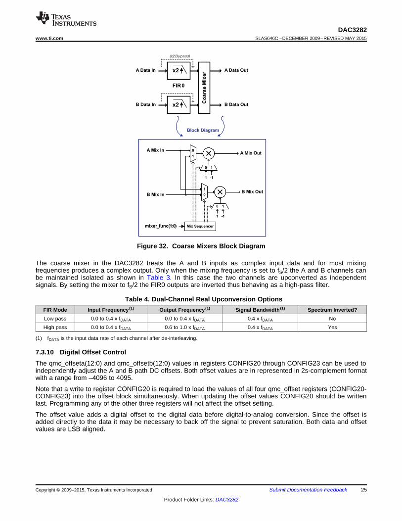
7.3.9 Coarse MixerThe DAC3282 has a coarse mixer block capable of shifting the input signal spectrum by the fixed mixingfrequencies fS/2 or ±fS/4. The coarse mixing function is built into the interpolation filter and thus FIR0 must beenabled to use it.
Treating channels A and B as a complex vector of the form I(t) + j Q(t), where I(t) = A(t) and Q(t) = B(t), theoutputs of the coarse mixer, AOUT(t) and BOUT(t) are equivalent to:
(1)
(2)
where fCMIX is the fixed mixing frequency selected by mixer_func(1:0). For fS/2, +fS/4 and –fS/4 the aboveoperations result in the simple mixing sequences shown in Table 3.
Table 3. Coarse Mixer SequencesMode mixer_func(1:0) Mixing SequenceNormal 00 AOUT = +A, +A , +A, +A (Low Pass, No Mixing) BOUT = +B, +B , +B, +B fS/2 01 AOUT = +A, –A , +A, –A
BOUT = +B, –B , +B, –B +fS/4 10 AOUT = +A, –B , –A, +B
BOUT = +B, +A , –B, –A –fS/4 11 AOUT = +A, +B , –A, –B
BOUT = +B, –A , –B, +A
24 Submit Documentation Feedback Copyright © 2009–2015, Texas Instruments Incorporated
Product Folder Links: DAC3282
x2
x2
FIR0
(x2Bypass)
Co
ars
eM
ixe
rA Data In
B Data In
A Data Out
B Data Out
Block Diagram
0
1
0 1
1 -1
0
1
0 1
1 -1
Mix Sequencermixer_func(1:0)
A Mix In
B Mix In
A Mix Out
B Mix Out
DAC3282www.ti.com SLAS646C –DECEMBER 2009–REVISED MAY 2015
Figure 32. Coarse Mixers Block Diagram
The coarse mixer in the DAC3282 treats the A and B inputs as complex input data and for most mixingfrequencies produces a complex output. Only when the mixing frequency is set to fS/2 the A and B channels canbe maintained isolated as shown in Table 3. In this case the two channels are upconverted as independentsignals. By setting the mixer to fS/2 the FIR0 outputs are inverted thus behaving as a high-pass filter.
Table 4. Dual-Channel Real Upconversion OptionsFIR Mode Input Frequency (1) Output Frequency (1) Signal Bandwidth (1) Spectrum Inverted?Low pass 0.0 to 0.4 x fDATA 0.0 to 0.4 x fDATA 0.4 x fDATA NoHigh pass 0.0 to 0.4 x fDATA 0.6 to 1.0 x fDATA 0.4 x fDATA Yes
(1) fDATA is the input data rate of each channel after de-interleaving.
7.3.10 Digital Offset ControlThe qmc_offseta(12:0) and qmc_offsetb(12:0) values in registers CONFIG20 through CONFIG23 can be used toindependently adjust the A and B path DC offsets. Both offset values are in represented in 2s-complement formatwith a range from –4096 to 4095.
Note that a write to register CONFIG20 is required to load the values of all four qmc_offset registers (CONFIG20-CONFIG23) into the offset block simultaneously. When updating the offset values CONFIG20 should be writtenlast. Programming any of the other three registers will not affect the offset setting.
The offset value adds a digital offset to the digital data before digital-to-analog conversion. Since the offset isadded directly to the data it may be necessary to back off the signal to prevent saturation. Both data and offsetvalues are LSB aligned.
Copyright © 2009–2015, Texas Instruments Incorporated Submit Documentation Feedback 25
Product Folder Links: DAC3282

S
13
qmc_offseta
-4096, -4095, … , 4095
A Data In
S
13qmc_offsetb
-4096, -4095, … , 4095
B Data In
A Data Out
B Data Out
16
16
16
16
DAC3282SLAS646C –DECEMBER 2009–REVISED MAY 2015 www.ti.com
Figure 33. Digital Offset Block Diagram
7.3.11 Temperature SensorThe DAC3282 incorporates a temperature sensor block which monitors the temperature by measuring thevoltage across 2 transistors. The voltage is converted to an 8-bit digital word using a successive-approximation(SAR) analog to digital conversion process. The result is scaled, limited and formatted as a twos complementvalue representing the temperature in degrees Celsius.
The sampling is controlled by the serial interface signals SDENB and SCLK. If the temperature sensor is enabled(tsense_ena = 1 in register CONFIG24) a conversion takes place each time the serial port is written or read. Thedata is only read and sent out by the digital block when the temperature sensor is read in register CONFIG5. Theconversion uses the first eight clocks of the serial clock as the capture and conversion clock, the data is valid onthe falling eighth SCLK. The data is then clocked out of the chip on the rising edge of the ninth SCLK. No otherclocks to the chip are necessary for the temperature sensor operation. As a result the temperature sensor isenabled even when the device is in sleep mode.
In order for the process described above to operate properly, the serial port read from CONFIG5 must be donewith an SCLK period of at least 1 µs. If this is not satisfied the temperature sensor accuracy is greatly reduced.
7.3.12 Sleep ModesThe DAC3282 features independent sleep control of each DAC (sleepa and sleepb), their corresponding clockpath (clkpath_sleep_a and clkpath_sleep_b) as well as the clock input receiver of the device (clkrecv_sleep). Thesleep control of each of these components is done through the SIF interface and is enabled by setting a 1 to thecorresponding sleep register.
Complete power down of the device is set by setting all of these components to sleep. Under this mode thesupply power consumption is reduced to 15mW. Power-up time in this case will be in the milliseconds range.Alternatively for those applications were power-up and power-down times are critical it is recommended to onlyset the DACs to sleep through the sleepa and sleepb registers. In this case both the sleep and wake-up timesare only 90µs.
7.3.13 Reference OperationThe DAC3282 uses a bandgap reference and control amplifier for biasing the full-scale output current. The full-scale output current is set by applying an external resistor RBIAS to pin BIASJ. The bias current IBIAS throughresistor RBIAS is defined by the on-chip bandgap reference voltage and control amplifier. The default full-scaleoutput current equals 16 times this bias current and can thus be expressed as:
IOUTFS = 16 × IBIAS = 16 × VEXTIO / RBIAS
Each DAC has a 4-bit independent coarse gain control via coarse_daca(3:0) and coarse_dacb (3:0) in theCONFIG4 register. Using gain control, the IOUTFS can be expressed as:
IOUTAFS = (DACA_gain + 1) × IBIAS = (DACA_gain + 1) × VEXTIO / RBIASIOUTBFS = (DACB_gain + 1) × IBIAS = (DACB_gain + 1) × VEXTIO / RBIAS
26 Submit Documentation Feedback Copyright © 2009–2015, Texas Instruments Incorporated
Product Folder Links: DAC3282

DACCLKP
OSTRP
DACCLKN
OSTRN
GND
666 W
2 kW
CLKVDD
Note: Input common mode level is
approximately 2/3*CLKVDD18,
or 1.2V nominal.
2 kW
333 W
DATACLKP /N
(DDR)
FRAMEP/N
D[7:0]P/N
SAMPLE 0 SAMPLE 1
t(FRAME)
I0[15:8]
I0[7:0]
Q0
[15:8]
Q0
[7:0]
I1[15:8]
I1[7:0]
Q1
[15:8]
Q1
[7:0]
DAC3282www.ti.com SLAS646C –DECEMBER 2009–REVISED MAY 2015
Where VEXTIO is the voltage at terminal EXTIO. The bandgap reference voltage delivers an accurate voltage of1.2V. This reference is active when extref_ena = ‘0’ in CONFIG25. An external decoupling capacitor CEXT of 0.1μF should be connected externally to terminal EXTIO for compensation. The bandgap reference can additionallybe used for external reference operation. In that case, an external buffer with high impedance input should beapplied in order to limit the bandgap load current to a maximum of 100 nA. The internal reference can bedisabled and overridden by an external reference by setting the CONFIG25 extref_ena control bit. Capacitor CEXTmay hence be omitted. Terminal EXTIO thus serves as either input or output node.
The full-scale output current can be adjusted from 20 mA down to 2 mA by varying resistor RBIAS or changing theexternally applied reference voltage. The internal control amplifier has a wide input range, supporting the full-scale output current range of 20 dB.
7.4 Device Functional Modes
7.4.1 Data InterfaceThe DAC3282 has a single 8-bit LVDS bus that accepts dual, 16-bit data input in byte-wide format. Data into theDAC3282 is formatted according to the diagram shown in Figure 34 where index 0 is the data LSB and index 15is the data MSB. The data is sampled by DATACLK, a double data rate (DDR) clock.
The FRAME signal is required to indicate the beginning of a frame. The frame signal can be either a pulse or aperiodic signal where the frame period corresponds to 8 samples. The pulse-width (t(FRAME)) needs to be at leastequal to ½ the DATACLK period. FRAME is sampled by a rising edge in DATACLK.
The setup and hold requirements listed in the specifications tables must be met to ensure proper sampling.
Figure 34. Byte-Wide Data Transmission Format
7.4.2 LVPECL InputsFigure 35 shows an equivalent circuit for the DAC input clock (DACCLKP/N) and the FIFO output strobe clock(OSTRP/N).
Figure 35. DACCLKP/N and OSTRP/N Equivalent Input Circuit
Copyright © 2009–2015, Texas Instruments Incorporated Submit Documentation Feedback 27
Product Folder Links: DAC3282
D[7:0]P,
DATACLKP ,
FRAMEP
100 LVDS
Receiver
DAC3282
D[7:0]N,
DATACLKN ,
FRAMENGND
VCOM =
(VA+VB)/2VB
VA,B
VA
VA
VB
VA,B
Logical Bit
Equivalent
1.40V
1.00V
400mV
0V
-400mV
1
0
Example
D[7:0]P,
DATACLKP ,
FRAMEP
50
D[7:0]N,
DATACLKN ,
FRAMEN
50
LVDS
Receiver
100pF
Total
To Adjacent
LVDS Input
To Adjacent
LVDS Input
Ref Note (1)
Note (1): RCENTER node common
to the D[7:0] P/N, DATACLKP / N and
FRAMEP/N receiver inputs
0.1 mF
CLKIN
CLKINC
0.1 mF
CAC
Differential
ECL
or
(LV)PECL
source
+
-
RT150 W150 W
100 W
DAC3282SLAS646C –DECEMBER 2009–REVISED MAY 2015 www.ti.com
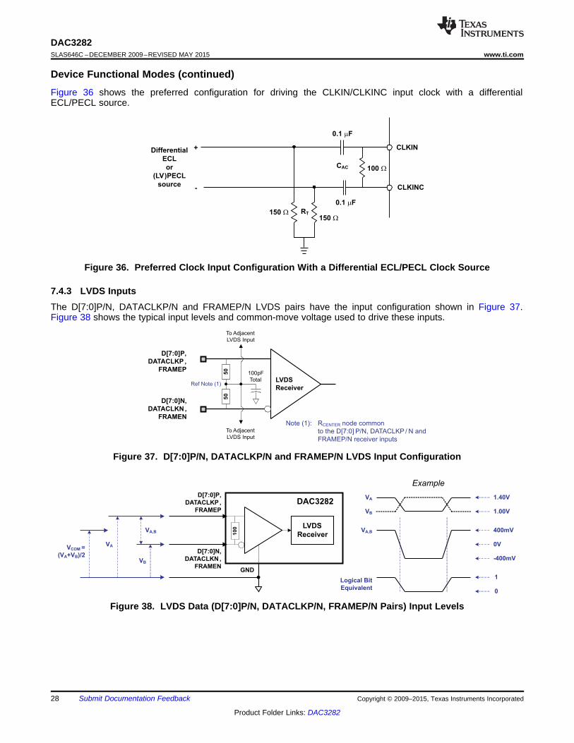
Device Functional Modes (continued)Figure 36 shows the preferred configuration for driving the CLKIN/CLKINC input clock with a differentialECL/PECL source.
Figure 36. Preferred Clock Input Configuration With a Differential ECL/PECL Clock Source
7.4.3 LVDS InputsThe D[7:0]P/N, DATACLKP/N and FRAMEP/N LVDS pairs have the input configuration shown in Figure 37.Figure 38 shows the typical input levels and common-move voltage used to drive these inputs.
Figure 37. D[7:0]P/N, DATACLKP/N and FRAMEP/N LVDS Input Configuration
Figure 38. LVDS Data (D[7:0]P/N, DATACLKP/N, FRAMEP/N Pairs) Input Levels
28 Submit Documentation Feedback Copyright © 2009–2015, Texas Instruments Incorporated
Product Folder Links: DAC3282
SDIOSCLK
TXENABLE
internal
digital in
DIGVDD 18
GND
SDENB
RESETB
internal
digital in
DIGVDD 18
GND
DAC3282www.ti.com SLAS646C –DECEMBER 2009–REVISED MAY 2015
Table 5. Example LVDS Data Input LevelsResultingResulting DifferentialApplied Voltages Common-Mode Logical Bit BinaryVoltage Voltage Equivalent
VA VB VA,B VCOM
1.4 V 1.0 V 400 mV 11.2 V
1.0 V 1.4 V –400 mV 01.2 V 0.8 V 400 mV 1
1.0 V0.8 V 1.2 V –400 mV 0
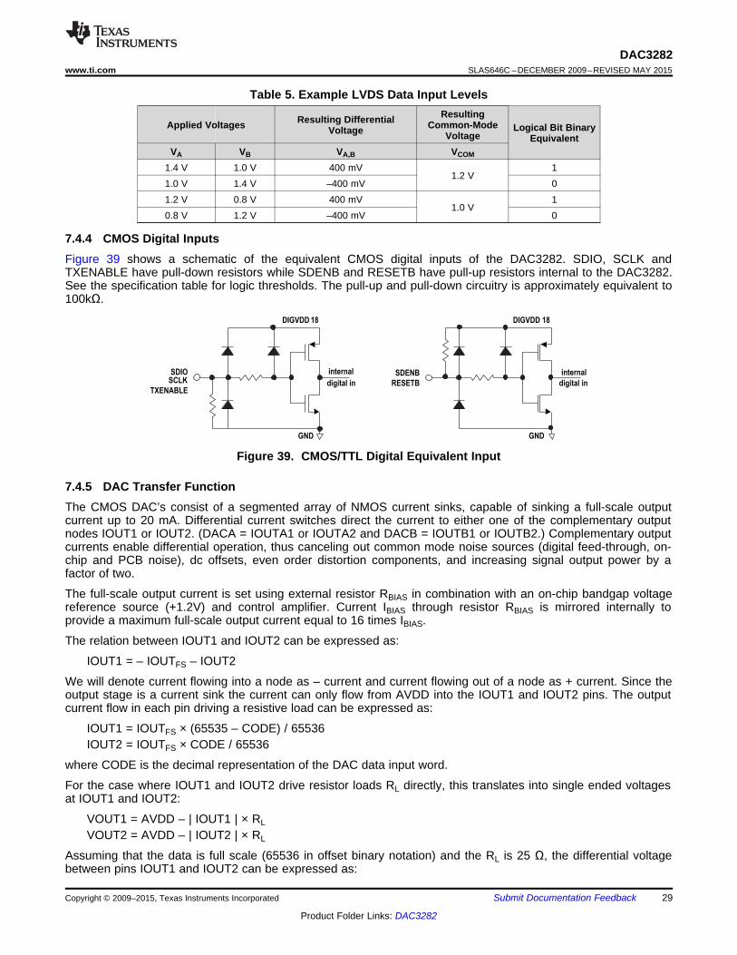
7.4.4 CMOS Digital InputsFigure 39 shows a schematic of the equivalent CMOS digital inputs of the DAC3282. SDIO, SCLK andTXENABLE have pull-down resistors while SDENB and RESETB have pull-up resistors internal to the DAC3282.See the specification table for logic thresholds. The pull-up and pull-down circuitry is approximately equivalent to100kΩ.
Figure 39. CMOS/TTL Digital Equivalent Input
7.4.5 DAC Transfer FunctionThe CMOS DAC’s consist of a segmented array of NMOS current sinks, capable of sinking a full-scale outputcurrent up to 20 mA. Differential current switches direct the current to either one of the complementary outputnodes IOUT1 or IOUT2. (DACA = IOUTA1 or IOUTA2 and DACB = IOUTB1 or IOUTB2.) Complementary outputcurrents enable differential operation, thus canceling out common mode noise sources (digital feed-through, on-chip and PCB noise), dc offsets, even order distortion components, and increasing signal output power by afactor of two.
The full-scale output current is set using external resistor RBIAS in combination with an on-chip bandgap voltagereference source (+1.2V) and control amplifier. Current IBIAS through resistor RBIAS is mirrored internally toprovide a maximum full-scale output current equal to 16 times IBIAS.
The relation between IOUT1 and IOUT2 can be expressed as:
IOUT1 = – IOUTFS – IOUT2
We will denote current flowing into a node as – current and current flowing out of a node as + current. Since theoutput stage is a current sink the current can only flow from AVDD into the IOUT1 and IOUT2 pins. The outputcurrent flow in each pin driving a resistive load can be expressed as:
IOUT1 = IOUTFS × (65535 – CODE) / 65536IOUT2 = IOUTFS × CODE / 65536
where CODE is the decimal representation of the DAC data input word.
For the case where IOUT1 and IOUT2 drive resistor loads RL directly, this translates into single ended voltagesat IOUT1 and IOUT2:
VOUT1 = AVDD – | IOUT1 | × RLVOUT2 = AVDD – | IOUT2 | × RL
Assuming that the data is full scale (65536 in offset binary notation) and the RL is 25 Ω, the differential voltagebetween pins IOUT1 and IOUT2 can be expressed as:
Copyright © 2009–2015, Texas Instruments Incorporated Submit Documentation Feedback 29
Product Folder Links: DAC3282
DAC3282SLAS646C –DECEMBER 2009–REVISED MAY 2015 www.ti.com
VOUT1 = AVDD – | –0mA | × 25 Ω = 3.3 VVOUT2 = AVDD – | –20mA | × 25 Ω = 2.8 VVDIFF = VOUT1 – VOUT2 = 0.5V
Note that care should be taken not to exceed the compliance voltages at node IOUT1 and IOUT2, which wouldlead to increased signal distortion.
7.5 Programming
7.5.1 Serial InterfaceThe serial port of the DAC3282 is a flexible serial interface which communicates with industry standardmicroprocessors and microcontrollers. The interface provides read/write access to all registers used to define theoperating modes of DAC3282. It is compatible with most synchronous transfer formats and can be configured asa 3 or 4 pin interface by sif4_ena in register CONFIG23. In both configurations, SCLK is the serial interface inputclock and SDENB is serial interface enable. For 3 pin configuration, SDIO is a bidirectional pin for both data inand data out. For 4 pin configuration, SDIO is bidirectional and ALARM_SDO is data out only. Data is input intothe device with the rising edge of SCLK. Data is output from the device on the falling edge of SCLK.
Each read/write operation is framed by signal SDENB (Serial Data Enable Bar) asserted low for 2 to 5 bytes,depending on the data length to be transferred (1–4 bytes). The first frame byte is the instruction cycle whichidentifies the following data transfer cycle as read or write, how many bytes to transfer, and what address totransfer the data. Table 6 indicates the function of each bit in the instruction cycle and is followed by a detaileddescription of each bit. Frame bytes 2 to 5 comprise the data transfer cycle.
Table 6. Instruction Byte of the Serial InterfaceMSB LSB
Bit 7 6 5 4 3 2 1 0Description R/W N1 N0 A4 A3 A2 A1 A0
R/W Identifies the following data transfer cycle as a read or write operation. A high indicates a readoperation from DAC3282 and a low indicates a write operation to DAC3282.
[N1 : N0] Identifies the number of data bytes to be transferred per Table 7. Data is transferred MSB first.
Table 7. Number of Transferred Bytes Within OneCommunication Frame
N1 N0 Description0 0 Transfer 1 Byte0 1 Transfer 2 Bytes1 0 Transfer 3 Bytes1 1 Transfer 4 Bytes
[A4 : A0] Identifies the address of the register to be accessed during the read or write operation. For multi-byte transfers, this address is the starting address. Note that the address is written to theDAC3282 MSB first and counts down for each byte.
Figure 40 shows the serial interface timing diagram for a DAC3282 write operation. SCLK is the serial interfaceclock input to DAC3282. Serial data enable SDENB is an active low input to DAC3282. SDIO is serial data in.Input data to DAC3282 is clocked on the rising edges of SCLK.
30 Submit Documentation Feedback Copyright © 2009–2015, Texas Instruments Incorporated
Product Folder Links: DAC3282

rwb N1 N0 - A3 A2 A1 A0 D7 D6 D5 D4 D3 D2 D1 D0
Instruction Cycle Data Transfer Cycle
td (Data)
SDENB
SCLK
SDIO
SDENB
SCLK
SDIO or
ALARM_SDO
D7 D6 D5 D4 D3 D2 D1 D0ALARM_
SDO
Data n Data n-1
3-pin interface
4-pin interface
rwb N1 N0 - A3 A2 A1 A0 D7 D6 D5 D4 D3 D2 D1 D0
Instruction Cycle Data Transfer Cycle
tS(SDENB)
tS(SDIO) tH(SDIO)
tSCLK
tSCLKH tSCLKL
SDENB
SCLK
SDIO
SDENB
SCLK
SDIO
DAC3282www.ti.com SLAS646C –DECEMBER 2009–REVISED MAY 2015
Figure 40. Serial Interface Write Timing Diagram
Figure 41 shows the serial interface timing diagram for a DAC3282 read operation. SCLK is the serial interfaceclock input to DAC3282. Serial data enable SDENB is an active low input to DAC3282. SDIO is serial data induring the instruction cycle. In 3 pin configuration, SDIO is data out from DAC3282 during the data transfercycle(s), while ALARM_SDO is in a high-impedance state. In 4 pin configuration, both ALARM_SDO and SDIOare data out from DAC3282. At the end of the data transfer, ALARM_SDO will output low on the final falling edgeof SCLK until the rising edge of SDENB when it will 3-state.
Figure 41. Serial Interface Read Timing Diagram
Copyright © 2009–2015, Texas Instruments Incorporated Submit Documentation Feedback 31
Product Folder Links: DAC3282

DAC3282SLAS646C –DECEMBER 2009–REVISED MAY 2015 www.ti.com
7.6 Register Maps
Table 8. Register Descriptions(MSB) (LSB)Name Address Default Bit 6 Bit 5 Bit 4 Bit 3 Bit 2 Bit 1Bit 7 Bit 0
CONFIG0 0x00 0x70 qmc_offset_ena fifo_ena fifo_reset_ena multi_sync_ena alarm_out_ena alarm_pol mixer_func(1:0)
CONFIG1 0x01 0x11 unused unused unused fir_ena fir4_ena iotest_ena unused twos
CONFIG2 0x02 0x00 unused unused unused unused output_delay(3:0)
alarm_ alarm_CONFIG3 0x03 0x10 64cnt_ena unused unused fifo_offset(2:0) 2away_ena 1away_ena
CONFIG4 0x04 0XFF coarse_daca(3:0) coarse_dacb(3:0)
CONFIG5 0x05 N/A tempdata(7:0)
CONFIG6 0x06 0x00 unused alarm_mask(6:0)
alarm_from_ alarm_fifo_ alarm_fifo_ alarm_fifo_CONFIG7 0x07 0x00 unused reserved alarm_from_ iotest unusedzerochk collision 2away 1away
CONFIG8 0x08 0x00 iotest_results(7:0)
CONFIG9 0x09 0x7A iotest_pattern0(7:0)
CONFIG10 0x0A 0xB6 iotest_pattern1(7:0)
CONFIG11 0x0B 0xEA iotest_pattern2(7:0)
CONFIG12 0x0C 0x45 iotest_pattern3(7:0)
CONFIG13 0x0D 0x1A iotest_pattern4(7:0)
CONFIG14 0x0E 0x16 iotest_pattern5(7:0)
CONFIG15 0x0F 0xAA iotest_pattern6(7:0)
CONFIG16 0x10 0xC6 iotest_pattern7(7:0)
CONFIG17 0x11 0x00 reserved reserved reserved reserved
daca_ dacb_ clkdiv_CONFIG18 0x12 0x02 reserved reserved unusedcomplement complement sync_ena
multi_CONFIG19 0x13 0x00 bequalsa aequalsb reserved unused unused unused revsync_sel
CONFIG20 0x14 0x00 qmc_offseta(7:0)
CONFIG21 0x15 0x00 qmc_offsetb(7:0)
CONFIG22 0x16 0x00 qmc_offseta(12:8) unused unused unused
clkpath_ clkpath_CONFIG23 0x17 0x00 qmc_offsetb(12:8) sif4_ena sleep_a sleep_b
CONFIG24 0x18 0x83 tsense_ena clkrecv_sleep unused reserved sleepb sleepa reserved reserved
CONFIG25 0x19 0x00 reserved extref_ena reserved reserved
CONFIG26 0x1A 0x00 unused unused unused unused unused reserved
CONFIG27 0x1B 0x00 reserved
CONFIG28 0x1C 0x00 reserved
CONFIG29 0x1D 0x00 reserved
CONFIG30 0x1E 0x00 reserved
VERSION31 0x1F 0x43 deviceid(1:0) version(5:0)
32 Submit Documentation Feedback Copyright © 2009–2015, Texas Instruments Incorporated
Product Folder Links: DAC3282

DAC3282www.ti.com SLAS646C –DECEMBER 2009–REVISED MAY 2015
7.6.1 CONFIG0 (address = 0x00) [reset = 0x70]
Figure 42. CONFIG0
7 6 5 4 3 2 1 0qmc_offset_ena fifoin_ena fifo_reset_ena multi_sync_ena alarm_out_ena alarm_pol mixer_func
R/W R/W R/W R/W R/W R/W R/W R/WLEGEND: R/W = Read/Write; R = Read only; -n = value after reset
Table 9. CONFIG0 Field DescriptionsBit Field Type Reset Description7 qmc_offset_ena R/W 0 When asserted the DAC offset correction is enabled.6 fifo_ena R/W 1 When asserted the FIFO is enabled. When the FIFO is bypassed
DACCCLKP/N and DATACLKP/N must be aligned to within t_align.5 fifo_reset_ena R/W 1 Allows the FRAME input to reset the FIFO write pointer when asserted4 multi_sync_ena R/W 1 Allows the FRAME or OSTR signal to reset the FIFO read pointer when
asserted. This selection is determined by multi_sync_sel in register CONFIG19.3 alarm_out_ena R/W 0 When asserted the ALARM_SDO pin becomes an output. The functionality of
this pin is controlled by the CONFIG6 alarm_mask setting.2 alarm_pol R/W 0 This bit changes the polarity of the ALARM signal. (0=negative logic, 1=positive
logic)1:0 mixer_func R/W 00 Controls the function of the mixer block.
Mode mixer_func(1:0)Normal 00
High Pass (Fs/2) 01Fs/4 10–Fs/4 11
7.6.2 CONFIG1 (address = 0x01) [reset = 0x11]
Figure 43. CONFIG1
7 6 5 4 3 2 1 0Unused Unused Unused fir_ena fir4_ena iotest_ena Unused twos
R/W R/W R/W R/W R/W R/W R/W R/WLEGEND: R/W = Read/Write; R = Read only; -n = value after reset
Table 10. CONFIG1 Field DescriptionsBit Field Type Reset Description7 Unused R/W 0 Reserved for factory use6 Unused R/W 0 Reserved for factory use.5 Unused R/W 0 Reserved for factory use4 fir_ena R/W 1 When asserted the chip does 2X interpolation of the data.3 fir4_ena R/W 0 When asserted, the zero-IF sinc correction filter is enabled. This filter cannot
be used unless fir_ena is asserted.2 iotest_ena R/W 0 When asserted enables the data pattern checker operation.1 Unused R/W 0 Reserved for factory use.0 twos R/W 1 When asserted the inputs are expected to be in 2's complement format. When
de-asserted the input format is expected to be offset-binary.
Copyright © 2009–2015, Texas Instruments Incorporated Submit Documentation Feedback 33
Product Folder Links: DAC3282

DAC3282SLAS646C –DECEMBER 2009–REVISED MAY 2015 www.ti.com
7.6.3 CONFIG2 (address = 0x02) [reset = 0x00]
Figure 44. CONFIG2
7 6 5 4 3 2 1 0Unused Unused Unused Unused output_delay
R/W R/W R/W R/W R/W R/W R/W R/WLEGEND: R/W = Read/Write; R = Read only; -n = value after reset
Table 11. CONFIG2 Field DescriptionsBit Field Type Reset Description7 Unused R/W 0 Reserved for factory use.6 Unused R/W 0 Reserved for factory use.5 Unused R/W 0 Reserved for factory use.4 Unused R/W 0 Reserved for factory use.
3:0 output_delay R/W 0000 Delays the output to the DACs from 0 to 15 DAC clock cycles.
7.6.4 CONFIG3 (address = 0x03) [reset = 0x10]
Figure 45. CONFIG3
7 6 5 4 3 2 1 064cnt_ena Unused Unused fifo_offset alarm_2away_ena alarm_1away_ena
R/W R/W R/W R/W R/W R/W R/W R/WLEGEND: R/W = Read/Write; R = Read only; -n = value after reset
Table 12. CONFIG3 Field DescriptionsBit Field Type Reset Description7 64cnt_ena R/W 0 This enables resetting the alarms after 64 good samples with the
goal of removing unnecessary errors. For instance, when checkingsetup/hold through the pattern checker test, there may initially beerrors. Setting this bit removes the need for a SIF write to clear thealarm register.
6 Unused R/W 0 Reserved for factory use.5 Unused R/W 0 Reserved for factory use.
4:2 fifo_offset R/W 100 This is the default FIFO read pointer position after the FIFO readpointer has been synced. With this value the initial differencebetween write and read pointers can be controlled. This may behelpful in controlling the delay through the device.
1 alarm_2away_ena R/W 0 When asserted alarms from the FIFO that represent the write andread pointers being 2 away are enabled.
0 alarm_1away_ena R/W 0 When asserted alarms from the FIFO that represent the write andread pointers being 1 away are enabled.
34 Submit Documentation Feedback Copyright © 2009–2015, Texas Instruments Incorporated
Product Folder Links: DAC3282
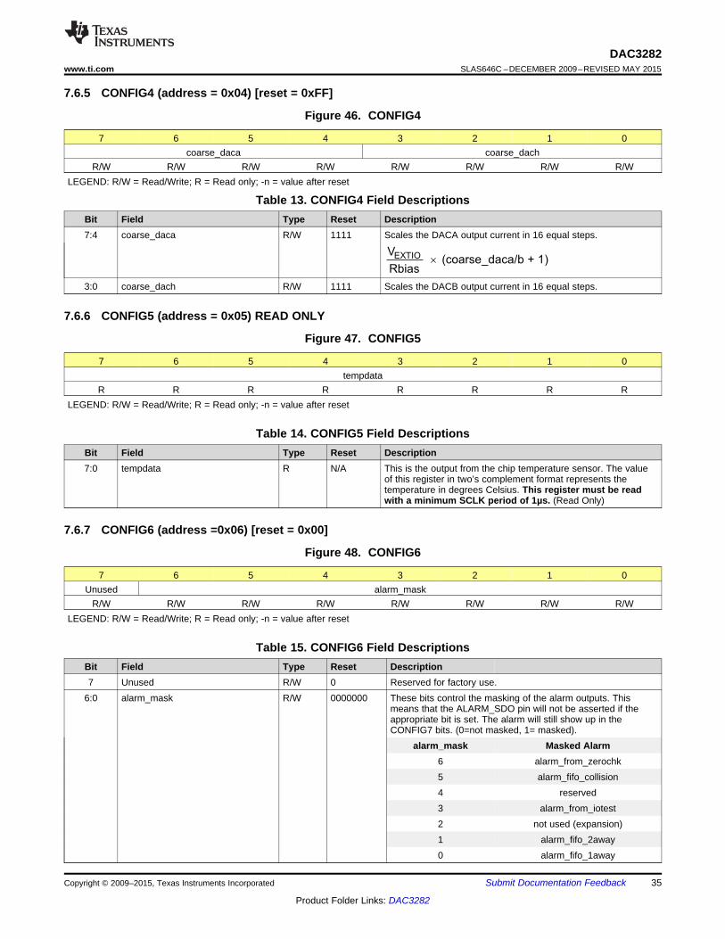
EXTIOV(coarse_daca/b + 1)
Rbias´
DAC3282www.ti.com SLAS646C –DECEMBER 2009–REVISED MAY 2015
7.6.5 CONFIG4 (address = 0x04) [reset = 0xFF]
Figure 46. CONFIG4
7 6 5 4 3 2 1 0coarse_daca coarse_dach
R/W R/W R/W R/W R/W R/W R/W R/WLEGEND: R/W = Read/Write; R = Read only; -n = value after reset
Table 13. CONFIG4 Field DescriptionsBit Field Type Reset Description7:4 coarse_daca R/W 1111 Scales the DACA output current in 16 equal steps.
3:0 coarse_dach R/W 1111 Scales the DACB output current in 16 equal steps.
7.6.6 CONFIG5 (address = 0x05) READ ONLY
Figure 47. CONFIG5
7 6 5 4 3 2 1 0tempdata
R R R R R R R RLEGEND: R/W = Read/Write; R = Read only; -n = value after reset
Table 14. CONFIG5 Field DescriptionsBit Field Type Reset Description7:0 tempdata R N/A This is the output from the chip temperature sensor. The value
of this register in two’s complement format represents thetemperature in degrees Celsius. This register must be readwith a minimum SCLK period of 1µs. (Read Only)
7.6.7 CONFIG6 (address =0x06) [reset = 0x00]
Figure 48. CONFIG6
7 6 5 4 3 2 1 0Unused alarm_mask
R/W R/W R/W R/W R/W R/W R/W R/WLEGEND: R/W = Read/Write; R = Read only; -n = value after reset
Table 15. CONFIG6 Field DescriptionsBit Field Type Reset Description7 Unused R/W 0 Reserved for factory use.
6:0 alarm_mask R/W 0000000 These bits control the masking of the alarm outputs. Thismeans that the ALARM_SDO pin will not be asserted if theappropriate bit is set. The alarm will still show up in theCONFIG7 bits. (0=not masked, 1= masked).
alarm_mask Masked Alarm6 alarm_from_zerochk5 alarm_fifo_collision4 reserved3 alarm_from_iotest2 not used (expansion)1 alarm_fifo_2away0 alarm_fifo_1away
Copyright © 2009–2015, Texas Instruments Incorporated Submit Documentation Feedback 35
Product Folder Links: DAC3282
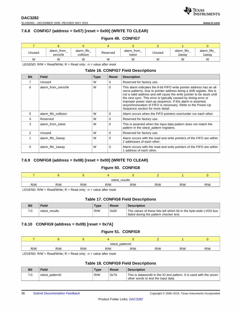
DAC3282SLAS646C –DECEMBER 2009–REVISED MAY 2015 www.ti.com
7.6.8 CONFIG7 (address = 0x07) [reset = 0x00] (WRITE TO CLEAR)
Figure 49. CONFIG7
7 6 5 4 3 2 1 0alarm_from_ alarm_fifo_ alarm_from_ alarm_fifo_ alarm_fifo_Unused Reserved Unusedzerochk collision iotest 2away 1away
W W W W W W W WLEGEND: R/W = Read/Write; R = Read only; -n = value after reset
Table 16. CONFIG7 Field DescriptionsBit Field Type Reset Description7 Unused W 0 Reserved for factory use.6 alarm_from_zerochk W 0 This alarm indicates the 8-bit FIFO write pointer address has an all
zeros patterns. Due to pointer address being a shift register, this isnot a valid address and will cause the write pointer to be stuck untilthe next sync. This error is typically caused by timing error orimproper power start-up sequence. If this alarm is asserted,resynchronization of FIFO is necessary. Refer to the Power-UpSequence section for more detail.
5 alarm_fifo_collision W 0 Alarm occurs when the FIFO pointers over/under run each other.4 Reserved W 0 Reserved for factory use.3 alarm_from_iotest W 0 This is asserted when the input data pattern does not match the
pattern in the iotest_pattern registers.2 Unused W 0 Reserved for factory use.1 alarm_fifo_2away W 0 Alarm occurs with the read and write pointers of the FIFO are within
2 addresses of each other.0 alarm_fifo_1away W 0 Alarm occurs with the read and write pointers of the FIFO are within
1 address of each other.
7.6.9 CONFIG8 (address = 0x08) [reset = 0x00] (WRITE TO CLEAR)
Figure 50. CONFIG8
7 6 5 4 3 2 1 0iotest_results
R/W R/W R/W R/W R/W R/W R/W R/WLEGEND: R/W = Read/Write; R = Read only; -n = value after reset
Table 17. CONFIG8 Field DescriptionsBit Field Type Reset Description7:0 iotest_results R/W 0x00 The values of these bits tell which bit in the byte-wide LVDS bus
failed during the pattern checker test.
7.6.10 CONFIG9 (address = 0x09) [reset = 0x7A]
Figure 51. CONFIG9
7 6 5 4 3 2 1 0iotest_pattern0
R/W R/W R/W R/W R/W R/W R/W R/WLEGEND: R/W = Read/Write; R = Read only; -n = value after reset
Table 18. CONFIG9 Field DescriptionsBit Field Type Reset Description7:0 iotest_pattern0 R/W 0x7A This is dataword0 in the IO test pattern. It is used with the seven
other words to test the input data.
36 Submit Documentation Feedback Copyright © 2009–2015, Texas Instruments Incorporated
Product Folder Links: DAC3282

DAC3282www.ti.com SLAS646C –DECEMBER 2009–REVISED MAY 2015
7.6.11 CONFIG10 (address = 0x0A) [reset = 0xB6]
Figure 52. CONFIG10
7 6 5 4 3 2 1 0iotest_pattern1
R/W R/W R/W R/W R/W R/W R/W R/WLEGEND: R/W = Read/Write; R = Read only; -n = value after reset
Table 19. CONFIG10 Field DescriptionsBit Field Type Reset Description7:0 iotest_pattern1 R/W 0xB6 This is dataword1 in the IO test pattern. It is used with the seven
other words to test the input data.
7.6.12 CONFIG11 (address = 0x0B) [reset = 0xEA]
Figure 53. CONFIG11
7 6 5 4 3 2 1 0iotest_pattern2
R/W R/W R/W R/W R/W R/W R/W R/WLEGEND: R/W = Read/Write; R = Read only; -n = value after reset
Table 20. CONFIG11 Field DescriptionsBit Field Type Reset Description7:0 iotest_pattern2 R/W 0xEA This is dataword2 in the IO test pattern. It is used with the seven
other words to test the input data.
7.6.13 CONFIG12 (address =0x0C) [reset = 0x45]
Figure 54. CONFIG12
7 6 5 4 3 2 1 0iotest_pattern3
R/W R/W R/W R/W R/W R/W R/W R/WLEGEND: R/W = Read/Write; R = Read only; -n = value after reset
Table 21. CONFIG12 Field DescriptionsBit Field Type Reset Description7:0 iotest_pattern3 R/W 0x45 This is dataword3 in the IO test pattern. It is used with the seven
other words to test the input data.
7.6.14 CONFIG13 (address =0x0D) [reset = 0x1A]
Figure 55. CONFIG13
7 6 5 4 3 2 1 0iotest_pattern4
R/W R/W R/W R/W R/W R/W R/W R/WLEGEND: R/W = Read/Write; R = Read only; -n = value after reset
Table 22. CONFIG13 Field DescriptionsBit Field Type Reset Description7:0 iotest_pattern4 R/W 0x1A This is dataword4 in the IO test pattern. It is used with the seven
other words to test the input data.
Copyright © 2009–2015, Texas Instruments Incorporated Submit Documentation Feedback 37
Product Folder Links: DAC3282

DAC3282SLAS646C –DECEMBER 2009–REVISED MAY 2015 www.ti.com
7.6.15 CONFIG14 Register Name (address = 0x0E) [reset = 0x16]
Figure 56. CONFIG14
7 6 5 4 3 2 1 0iotest_pattern5
R/W R/W R/W R/W R/W R/W R/W R/WLEGEND: R/W = Read/Write; R = Read only; -n = value after reset
Table 23. CONFIG14 Field DescriptionsBit Field Type Reset Description7:0 iotest_pattern5 R/W 0x16 This is dataword5 in the IO test pattern. It is used with the seven
other words to test the input data.
7.6.16 CONFIG15 Register Name (address = 0x0F) [reset = 0xAA]
Figure 57. CONFIG15
7 6 5 4 3 2 1 0iotest_pattern6
R/W R/W R/W R/W R/W R/W R/W R/WLEGEND: R/W = Read/Write; R = Read only; -n = value after reset
Table 24. CONFIG15 Field DescriptionsBit Field Type Reset Description7:0 iotest_pattern6 R/W 0xAA This is dataword6 in the IO test pattern. It is used with the seven
other words to test the input data.
7.6.17 CONFIG16 (address = 0x10) [reset = 0xC6]
Figure 58. CONFIG16
7 6 5 4 3 2 1 0iotest_pattern7
R/W R/W R/W R/W R/W R/W R/W R/WLEGEND: R/W = Read/Write; R = Read only; -n = value after reset
Table 25. CONFIG16 Field DescriptionsBit Field Type Reset Description7:0 iotest_pattern7 R/W 0xC6 This is dataword7 in the IO test pattern. It is used with the seven
other words to test the input data.
38 Submit Documentation Feedback Copyright © 2009–2015, Texas Instruments Incorporated
Product Folder Links: DAC3282
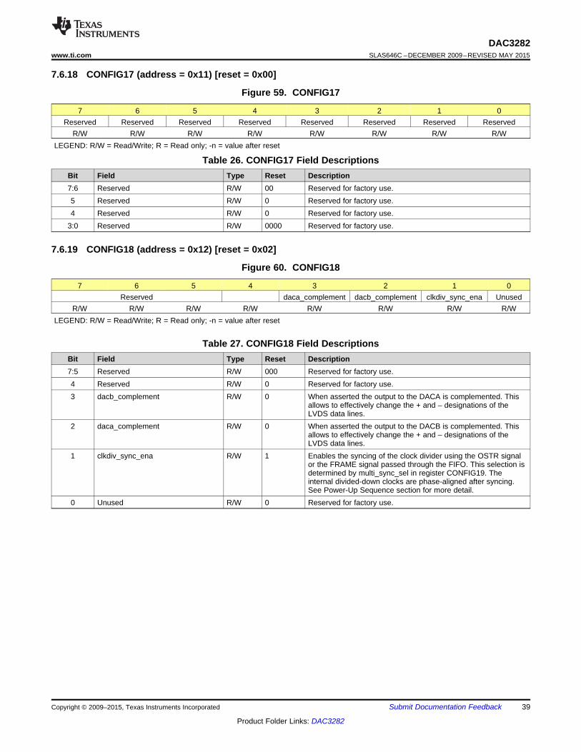
DAC3282www.ti.com SLAS646C –DECEMBER 2009–REVISED MAY 2015
7.6.18 CONFIG17 (address = 0x11) [reset = 0x00]
Figure 59. CONFIG17
7 6 5 4 3 2 1 0Reserved Reserved Reserved Reserved Reserved Reserved Reserved Reserved
R/W R/W R/W R/W R/W R/W R/W R/WLEGEND: R/W = Read/Write; R = Read only; -n = value after reset
Table 26. CONFIG17 Field DescriptionsBit Field Type Reset Description7:6 Reserved R/W 00 Reserved for factory use.5 Reserved R/W 0 Reserved for factory use.4 Reserved R/W 0 Reserved for factory use.
3:0 Reserved R/W 0000 Reserved for factory use.
7.6.19 CONFIG18 (address = 0x12) [reset = 0x02]
Figure 60. CONFIG18
7 6 5 4 3 2 1 0Reserved daca_complement dacb_complement clkdiv_sync_ena Unused
R/W R/W R/W R/W R/W R/W R/W R/WLEGEND: R/W = Read/Write; R = Read only; -n = value after reset
Table 27. CONFIG18 Field DescriptionsBit Field Type Reset Description7:5 Reserved R/W 000 Reserved for factory use.4 Reserved R/W 0 Reserved for factory use.3 dacb_complement R/W 0 When asserted the output to the DACA is complemented. This
allows to effectively change the + and – designations of theLVDS data lines.
2 daca_complement R/W 0 When asserted the output to the DACB is complemented. Thisallows to effectively change the + and – designations of theLVDS data lines.
1 clkdiv_sync_ena R/W 1 Enables the syncing of the clock divider using the OSTR signalor the FRAME signal passed through the FIFO. This selection isdetermined by multi_sync_sel in register CONFIG19. Theinternal divided-down clocks are phase-aligned after syncing.See Power-Up Sequence section for more detail.
0 Unused R/W 0 Reserved for factory use.
Copyright © 2009–2015, Texas Instruments Incorporated Submit Documentation Feedback 39
Product Folder Links: DAC3282

DAC3282SLAS646C –DECEMBER 2009–REVISED MAY 2015 www.ti.com
7.6.20 CONFIG19 (address = 0x13) [reset = 0x00]
Figure 61. CONFIG19
7 6 5 4 3 2 1 0bequalsa aequalsb Reserved Unused Unused Unused multi_sync_sel rev
R/W R/W R/W R/W R/W R/W R/W R/WLEGEND: R/W = Read/Write; R = Read only; -n = value after reset
Table 28. CONFIG19 Field DescriptionsBit Field Type Reset Description7 bequalsa R/W 0 When asserted the DACA data is driven onto DACB.6 aequalsb R/W 0 When asserted the DACB data is driven onto DACA.5 Reserved R/W 0 Reserved for factory use.4 Unused R/W 0 Reserved for factory use.3 Unused R/W 0 Reserved for factory use.2 Unused R/W 0 Reserved for factory use.1 multi_sync_sel R/W 0 Selects the signal source for multiple device and clock divider
synchronization.multi_sync_sel Sync Source
0 OSTR1 FRAME through FIFO handoff
0 rev R/W 0 Reverse the input bits for the data word. MSB becomes LSB.
7.6.21 CONFIG20 (address = 0x14) [reset = 0x00] (CAUSES AUTOSYNC)
Figure 62. CONFIG20
7 6 5 4 3 2 1 0qmc_offseta
R/W R/W R/W R/W R/W R/W R/W R/WLEGEND: R/W = Read/Write; R = Read only; -n = value after reset
Table 29. CONFIG20 Field DescriptionsBit Field Type Reset Description7:0 qmc_offseta R/W 0x00 Lower 8 bits of the DAC A offset correction. The offset is
measured in DAC LSBs. Writing this register causes anautosync to be generated. This loads the values of all fourqmc_offset registers (CONFIG20-CONFIG23) into the offsetblock at the same time. When updating the offset valuesCONFIG20 should be written last. Programming any of theother three registers will not affect the offset setting.
7.6.22 CONFIG21 (address = 0x15) [reset = 0x00]
Figure 63. CONFIG21
7 6 5 4 3 2 1 0qmc_offsetb
R/W R/W R/W R/W R/W R/W R/W R/WLEGEND: R/W = Read/Write; R = Read only; -n = value after reset
Table 30. CONFIG21 Field DescriptionsBit Field Type Reset Description7:0 qmc_offsetb R/W 0x00 Lower 8 bits of the DAC B offset correction. The offset is
measured in DAC LSBs.
40 Submit Documentation Feedback Copyright © 2009–2015, Texas Instruments Incorporated
Product Folder Links: DAC3282

DAC3282www.ti.com SLAS646C –DECEMBER 2009–REVISED MAY 2015
7.6.23 CONFIG22 (address = 0x16) [reset = 0x00]
Figure 64. CONFIG22
7 6 5 4 3 2 1 0qmc_offseta Unused Unused Unused
R/W R/W R/W R/W R/W R/W R/W R/WLEGEND: R/W = Read/Write; R = Read only; -n = value after reset
Table 31. CONFIG22 Field DescriptionsBit Field Type Reset Description7:3 qmc_offseta R/W 00000 Upper 5 bits of the DAC A offset correction.2 Unused R/W 0 Reserved for factory use.1 Unused R/W 0 Reserved for factory use.0 Unused R/W 0 Reserved for factory use.
7.6.24 CONFIG23 (address = 0x17) [reset = 0x00]
Figure 65. CONFIG23
7 6 5 4 3 2 1 0qmc_offsetb(12:8) sif4_ena clkpath_sleep_ clkpath_sleep_
a bR/W R/W R/W R/W R/W R/W R/W R/W
LEGEND: R/W = Read/Write; R = Read only; -n = value after reset
Table 32. CONFIG23 Field DescriptionsBit Field Type Reset Description7:3 qmc_offsetb(12:8) R/W 00000 Upper 5 bits of the DAC B offset correction.2 sif4_ena R/W 0 When asserted the SIF interface becomes a 4 pin interface. The
ALARM_SDO pin is turned into a dedicated output for thereading of data.
1 clkpath_sleep_a R/W 0 When asserted puts the clock path through DAC A to sleep. Thisis useful for sleeping individual DACs. Even if the DAC is asleepthe clock needs to pass through it for the logic to work.However, if the chip is being put into a power down mode, thenall parts of the DAC can be turned off.
0 clkpath_sleep_b R/W 0 When asserted puts the clock path through DAC B to sleep.
Copyright © 2009–2015, Texas Instruments Incorporated Submit Documentation Feedback 41
Product Folder Links: DAC3282

DAC3282SLAS646C –DECEMBER 2009–REVISED MAY 2015 www.ti.com
7.6.25 CONFIG24 (address = 0x18) [reset = 0x83]
Figure 66. CONFIG24
7 6 5 4 3 2 1 0tsense_ena clkrecv_sleep Unused Reserved sleepb sleepa Reserved Reserved
R/W R/W R/W R/W R/W R/W R/W R/WLEGEND: R/W = Read/Write; R = Read only; -n = value after reset
Table 33. CONFIG24 Field DescriptionsBit Field Type Reset Description7 tsense_ena R/W 1 Turns on the temperature sensor when asserted.6 clkrecv_sleep R/W 0 When asserted the clock input receiver gets put into sleep
mode. This also affects the OSTR receiver.5 Unused R/W 0 Reserved for factory use.4 Reserved R/W 0 Reserved for factory use.3 sleepb R/W 0 When asserted DACB is put into sleep mode.2 sleepa R/W 0 When asserted DACA is put into sleep mode.1 Reserved R/W 1 Reserved for factory use.0 Reserved R/W 1 Reserved for factory use.
7.6.26 CONFIG25 (address = 0x19) [reset = 0x00]
Figure 67. CONFIG25
7 6 5 4 3 2 1 0Reserved extref_ena Reserved Reserved
R/W R/W R/W R/W R/W R/W R/W R/WLEGEND: R/W = Read/Write; R = Read only; -n = value after reset
Table 34. CONFIG25 Field DescriptionsBit Field Type Reset Description7:3 Reserved R/W 00000 Reserved for factory use.2 extref_ena R/W 0 Allows the device to use an external reference or the internal
reference. (0=internal, 1=external)1 Reserved R/W 0 Reserved for factory use.0 Reserved R/W 0 Reserved for factory use.
7.6.27 CONFIG26 (address = 0x1A) [reset = 0x00]
Figure 68. CONFIG26
7 6 5 4 3 2 1 0Reserved Reserved Reserved Reserved Unused Reserved
R/W R/W R/W R/W R/W R/W R/W R/WLEGEND: R/W = Read/Write; R = Read only; -n = value after reset
Table 35. CONFIG26 Field DescriptionsBit Field Type Reset Description7 Reserved R/W 0 Reserved for factory use.6 Reserved R/W 0 Reserved for factory use.5 Reserved R/W 0 Reserved for factory use.5 Reserved R/W 0 Reserved for factory use.3 Unused R/W 0 Reserved for factory use.
2:0 Reserved R/W 000 Reserved for factory use.
42 Submit Documentation Feedback Copyright © 2009–2015, Texas Instruments Incorporated
Product Folder Links: DAC3282

DAC3282www.ti.com SLAS646C –DECEMBER 2009–REVISED MAY 2015
7.6.28 CONFIG27 (address =0x1B) [reset = 0x00]
Figure 69. CONFIG27
7 6 5 4 3 2 1 0Reserved
R/W R/W R/W R/W R/W R/W R/W R/WLEGEND: R/W = Read/Write; R = Read only; -n = value after reset
Table 36. CONFIG27 Field DescriptionsBit Field Type Reset Description7:0 Reserved R/W 0x00 Reserved for factory use.
7.6.29 CONFIG28 (address = 0x1C) [reset = 0x00]
Figure 70. CONFIG28
7 6 5 4 3 2 1 0Reserved
R/W R/W R/W R/W R/W R/W R/W R/WLEGEND: R/W = Read/Write; R = Read only; -n = value after reset
Table 37. CONFIG28 Field DescriptionsBit Field Type Reset Description7:0 Reserved R/W 0x00 Reserved for factory use.
7.6.30 CONFIG29 (address = 0x1D) [reset = 0x00]
Figure 71. CONFIG29
7 6 5 4 3 2 1 0Reserved
R/W R/W R/W R/W R/W R/W R/W R/WLEGEND: R/W = Read/Write; R = Read only; -n = value after reset
Table 38. CONFIG29 Field DescriptionsBit Field Type Reset Description7:0 Reserved R/W 0x00 Reserved for factory use.
Copyright © 2009–2015, Texas Instruments Incorporated Submit Documentation Feedback 43
Product Folder Links: DAC3282

DAC3282SLAS646C –DECEMBER 2009–REVISED MAY 2015 www.ti.com
7.6.31 CONFIG30 (address = 0x1E) [reset = 0x00]
Figure 72. CONFIG30
7 6 5 4 3 2 1 0Reserved
R/W R/W R/W R/W R/W R/W R/W R/WLEGEND: R/W = Read/Write; R = Read only; -n = value after reset
Table 39. CONFIG30 Field DescriptionsBit Field Type Reset Description7:0 Reserved R/W 0x00 Reserved for factory use.
7.6.32 VERSION31 (address = 0x1F) [reset = 0x43] (READ ONLY)
Figure 73. VERSION31
7 6 5 4 3 2 1 0deviceid version
R R R R R R R RLEGEND: R/W = Read/Write; R = Read only; -n = value after reset
Table 40. VERSION31 Field DescriptionsBit Field Type Reset Description7:0 deviceid(1:0) R 01 Returns ‘01’ for DAC3282. (Read Only)5:0 version(5:0) R 000011 A hardwired register that contains the version of the chip. (Read
Only)
44 Submit Documentation Feedback Copyright © 2009–2015, Texas Instruments Incorporated
Product Folder Links: DAC3282

Clock Generator
DATACLKP/N
FRAMEP/N
FPGAD[7:0]P/N
DATACLKP/N
FRAMEP/N
D[7:0]P/N
DACCLKP/N
LV
DS
Inte
rfa
ce
LVPECL Outputs
OSTRP/N
LVPECL Outputs
DACCLKP/N
OSTRP/N
PLL/DLL
DAC3282/3 DAC1
DAC3282/3 DAC2
delay 1
delay 2
Variable delays due to variations in theFPGA(s) output paths or board level wiringor temperature/voltage deltas
Outputs are
phase aligned
DAC3282www.ti.com SLAS646C –DECEMBER 2009–REVISED MAY 2015
8 Application and Implementation
NOTEInformation in the following applications sections is not part of the TI componentspecification, and TI does not warrant its accuracy or completeness. TI’s customers areresponsible for determining suitability of components for their purposes. Customers shouldvalidate and test their design implementation to confirm system functionality.
8.1 Application InformationThe DAC3282 is appropriate for a variety of transmitter applications including complex I/Q direct conversion, up-conversion using an intermediate frequency (IF) and diversity applications.
8.1.1 Multi-device SynchronizationIn various applications, such as multi antenna systems where the various transmit channels information iscorrelated, it is required that multiple DAC devices are completely synchronized such that their outputs are phasealigned. The DAC3282 architecture supports this mode of operation.
8.1.1.1 Multi-device Synchronization: Dual Sync Sources ModeFor single or multi-device synchronization it is important that delay differences in the data are absorbed by thedevice so that latency through the device remains the same. Furthermore, to guarantee that the outputs fromeach DAC are phase aligned it is necessary that data is read from the FIFO of each device simultaneously. Inthe DAC3282 this is accomplished by operating the multiple devices in Dual Sync Sources mode. In this modethe additional OSTR signal is required by each DAC3282 to be synchronized.
Data into the device is input as LVDS signals from one or multiple baseband ASICs or FPGAs. Data into themultiple DAC devices can experience different delays due to variations in the digital source output paths or boardlevel wiring. These different delays can be effectively absorbed by the DAC3282 FIFO so that all outputs arephase aligned correctly.
Figure 74. Synchronization System in Dual Sync Sources Mode with PLL Bypassed
For correct operation both OSTR and DACCLK must be generated from the same clock domain. The OSTRsignal is sampled by DACCLK and must satisfy the timing requirements in the specifications table. If the clockgenerator does not have the ability to delay the DACCLK to meet the OSTR timing requirement, the polarity ofthe DACCLK outputs can be swapped with respect to the OSTR ones to create 180 degree phase delay of theDACCLK. This may help establish proper setup and hold time requirement of the OSTR signal.
Copyright © 2009–2015, Texas Instruments Incorporated Submit Documentation Feedback 45
Product Folder Links: DAC3282

DACCLKP/N(2)
OSTRP/N(2)
LV
PE
CL
Pa
irs
(DA
C3
28
2/3
2)
ts(OSTR)
th(OSTR)
DACCLKP/N(1)
OSTRP/N(1)
LV
PE
CL
Pa
irs
(DA
C3
28
2/3
1)
ts(OSTR)
th(OSTR)
tSKEW ~ 0
DAC3282SLAS646C –DECEMBER 2009–REVISED MAY 2015 www.ti.com
Application Information (continued)Careful board layout planning must be done to ensure that the DACCLK and OSTR signals are distributed fromdevice to device with the lowest skew possible as this will affect the synchronization process. In order tominimize the skew across devices it is recommended to use the same clock distribution device to provide theDACCLK and OSTR signals to all the DAC devices in the system.
Figure 75. Timing Diagram for LVPECL Synchronization Signals
The following steps are required to ensure the devices are fully synchronized. The procedure assumes all theDAC3282 devices have a DACCLK and OSTR signal and must be carried out on each device.1. Start-up the device as described in the power-up sequence. Set the DAC3282 in Dual Sync Sources mode
and select OSTR as the FIFO output pointer sync source and clock divider sync source (multi_sync_sel inregister config19).
2. Sync the clock divider and FIFO pointers.3. Verify there are no FIFO alarms either through register config7 or through the ALARM_SDO pin.
After these steps all the DAC3282 outputs will be synchronized.
8.1.1.2 Multi-device Operation: Single Sync Source ModeIn Single Sync Source mode, the FIFO write and read pointers are reset from the same FRAME source.Although the FIFO in this mode can still absorb the data delay differences due to variations in the digital sourceoutput paths or board level wiring, it is impossible to guarantee data will be read from the FIFO of differentdevices simultaneously thus preventing exact phase alignment.
The FIFO read pointer reset is handoff between the two clock domains (DATACLK and FIFO OUT CLOCK) bysimply re-sampling the write pointer reset. Since the two clocks are asynchronous there is a small but distinctpossibility of a meta-stablility during the pointer handoff. This meta-stability can cause the outputs of the multipledevices to slip by up to 2 DAC clock cycles.
46 Submit Documentation Feedback Copyright © 2009–2015, Texas Instruments Incorporated
Product Folder Links: DAC3282

AVDD
S(1)
S(1)C
S(2)
S(2)C
S(N)
S(N)C
...
IOUT1 IOUT2
RLOAD RLOAD
Clock Generator
DATACLKP/N
FRAMEP/N
FPGAD[7:0]P/N
DATACLKP/N
FRAMEP/N
D[7:0]P/N
DACCLKP/N
LV
DS
Inte
rfa
ce
LVPECL Output
LVPECL Output
DACCLKP/N
PLL/DLL
DAC3282/3 DAC1
DAC3282/3 DAC2
delay 1
delay 2
Variable delays due to variations in theFPGA(s) output paths or board level wiringor temperature/voltage deltas
0 to 2
DAC Clock cycles
DAC3282www.ti.com SLAS646C –DECEMBER 2009–REVISED MAY 2015
Application Information (continued)
Figure 76. Multi-Device Operation in Single Sync Source Mode
8.1.2 Analog Current OutputsFigure 77 shows a simplified schematic of the current source array output with corresponding switches.Differential switches direct the current of each individual NMOS current source to either the positive output nodeIOUT1 or its complementary negative output node IOUT2. The output impedance is determined by the stack ofthe current sources and differential switches, and is typically >300 kΩ in parallel with an output capacitance of 5pF.
The external output resistors are referred to an external ground. The minimum output compliance at nodesIOUT1 and IOUT2 is limited to AVDD – 0.5 V, determined by the CMOS process. Beyond this value, transistorbreakdown may occur resulting in reduced reliability of the DAC3282 device. The maximum output compliancevoltage at nodes IOUT1 and IOUT2 equals AVDD + 0.5 V. Exceeding the minimum output compliance voltageadversely affects distortion performance and integral non-linearity. The optimum distortion performance for asingle-ended or differential output is achieved when the maximum full-scale signal at IOUT1 and IOUT2 does notexceed 0.5 V.
Figure 77. Equivalent Analog Current Output
Copyright © 2009–2015, Texas Instruments Incorporated Submit Documentation Feedback 47
Product Folder Links: DAC3282

IOUT 1
4 :1
50 W
RLOAD
100 W
IOUT 2
AVDD 3.3 V
AVDD 3.3 V
100 W
IOUT 1
1 : 1
IOUT 2
RLOAD100 W
50 W
AVDD
AVDD 3.3 V
3.3 V
50 W
50 W
DAC3282SLAS646C –DECEMBER 2009–REVISED MAY 2015 www.ti.com
Application Information (continued)The DAC3282 can be easily configured to drive a doubly terminated 50 Ω cable using a properly selected RFtransformer. Figure 78 and Figure 79 show the 50 Ω doubly terminated transformer configuration with 1:1 and 4:1impedance ratio, respectively. Note that the center tap of the primary input of the transformer has to beconnected to AVDD to enable a DC current flow. Applying a 20 mA full-scale output current would lead to a 0.5Vpp for a 1:1 transformer and a 1 Vpp output for a 4:1 transformer. The low dc-impedance between IOUT1 orIOUT2 and the transformer center tap sets the center of the ac-signal at AVDD, so the 1 Vpp output for the 4:1transformer results in an output between AVDD + 0.5 V and AVDD – 0.5 V.
Figure 78. Driving a Doubly Terminated 50 Ω Cable Using a 1:1 Impedance Ratio Transformer
Figure 79. Driving a Doubly Terminated 50 Ω Cable Using a 4:1 Impedance Ratio Transformer
48 Submit Documentation Feedback Copyright © 2009–2015, Texas Instruments Incorporated
Product Folder Links: DAC3282

I
/I
TRF3703-17
I
/I
V1
V1
R1
R1
R2
R2
R3
R3
V2DAC3282
IOUTA1
IOUTA2
IOUTB1
IOUTB2
S
RFS
ign
al
Co
nd
itio
nin
g
Quadrature modulator
Vout ~ 2.8 to 3.8 V Vin ~ Varies
I1
I2
Q1
Q2
DAC3282www.ti.com SLAS646C –DECEMBER 2009–REVISED MAY 2015
Application Information (continued)8.1.3 Passive Interface to Analog Quadrature ModulatorsA common application in communication systems is to interface the DAC to an IQ modulator like the TRF3703family of modulators from Texas Instruments. The input of the modulator is generally of high impedance andrequires a specific common-mode voltage. A simple resistive network can be used to maintain 50Ω loadimpedance for the DAC3282 and also provide the necessary common-mode voltages for both the DAC and themodulator.
Figure 80. DAC to Analog Quadrature Modulator Interface
The DAC3282 has a maximum 20mA full-scale output and a voltage compliance range of AVDD ± 0.5 V. TheTRF3703 IQ modulator family can be operated at three common-mode voltages: 1.5V, 1.7V, and 3.3V.
Figure 81 shows the recommended passive network to interface the DAC3282 to the TRF3703-17 which has acommon mode voltage of 1.7V. The network generates the 3.3V common mode required by the DAC output and1.7V at the modulator input, while still maintaining 50Ω load for the DAC.
Figure 81. DAC3282 to TRF3703-17 Interface
If V1 is set to 5V and V2 is set to -5V, the corresponding resistor values are R1 = 57Ω, R2 = 80Ω, and R3 =336Ω. The loss developed through R2 is about -1.86 dB. In the case where there is no –5V supply available andV2 is set to 0V, the resistor values are R1 = 66Ω, R2 = 101Ω, and R3 = 107Ω. The loss with these values is–5.76dB.
Figure 82 shows the recommended network for interfacing with the TRF3703-33 which requires a common modeof 3.3V. This is the simplest interface as there is no voltage shift. Because there is no voltage shift there isn't anyloss in the network. With V1 = 5V and V2 = 0V, the resistor values are R1 = 66Ω and R3 = 208Ω.
Copyright © 2009–2015, Texas Instruments Incorporated Submit Documentation Feedback 49
Product Folder Links: DAC3282

DAC3282
I
/I
TRF3703
V1
R1
R1
R3
R3
FilterR4
V1
R2
R2
V2
I
/I
TRF3703-33
I
/I
V1
V1
R1
R1
R3
R3
V2DAC3282
DAC3282SLAS646C –DECEMBER 2009–REVISED MAY 2015 www.ti.com
Application Information (continued)
Figure 82. DAC3282 to TRF3703-33 Interface
In most applications a baseband filter is required between the DAC and the modulator to eliminate the DACimages. This filter can be placed after the common-mode biasing network. For the DAC to modulator networkshown in Figure 83, R2 and the filter load R4 need to be considered into the DAC impedance. The filter has to bedesigned for the source impedance created by the resistor combination of R3 // (R2+R1). The effectiveimpedance seen by the DAC is affected by the filter termination resistor resulting in R1 // (R2+R3 // (R4/2)).
Figure 83. DAC3282 to Modulator Interface with Filter
Factoring in R4 into the DAC load, a typical interface to the TRF3703-17 with V1 = 5V and V2 = 0V results in thefollowing values: R1 = 72Ω, R2 = 116Ω, R3 = 124Ω and R4 = 150Ω. This implies that the filter needs to bedesigned for 75Ω input and output impedance (single-ended impedance). The common mode levels for the DACand modulator are maintained at 3.3V and 1.7V and the DAC load is 50Ω. The added load of the filtertermination causes the signal to be attenuated by –10.8 dB.
A filter can be implemented in a similar manner to interface with the TRF3703-33. In this case it is much simplerto balance the loads and common mode voltages due to the absence of R2. An added benefit is that there is noloss in this network. With V1 = 5V and V2 = 0V the network can be designed such that R1 = 115Ω, R3 = 681Ω,and R4 = 200Ω. This results in a filter impedance of R1 // R2=100Ω, and a DAC load of R1 // R3 // (R4/2) whichis equal to 50Ω. R4 is a differential resistor and does not affect the common mode level created by R1 and R3.The common-mode voltage is set at 3.3 V for a full-scale current of 20mA.
For more information on how to interface the DAC3282 to an analog quadrature modulator please refer to theapplication reports Passive Terminations for Current Output DACs (SLAA399) and Design of Differential Filtersfor High-Speed Signal Chains (SLWA053).
50 Submit Documentation Feedback Copyright © 2009–2015, Texas Instruments Incorporated
Product Folder Links: DAC3282
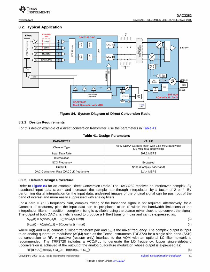
Div
DATACLKP /N
FRAMEP/N
DAC-A
Q-F
IR
CM
IX
I-F
IR
Q-
ISIN
CI-
ISIN
C
DA
CC
LK
P/N
DAC3282 DACFPGA
PFD/CP
CDCE62005
Clock Generator with VCO
VCON-Divider
R-Div
PFD
CPOUT
VCTRL_IN
900
TRF3720
AQM with PLL/VCO
LoopFilter
Div2/4/8
RF OUT
Op
tio
nal
Fil
ter
Ne
two
rk
LV
DS
Data
Inte
rface
LoopFilter
5V
D0P/N
D7P/N
Byte-Wide
Data
100
100
100
100
DAC-B
10 MHzOSC
Clock Divider/
Distribution
/1
Div
10
0
FIF
O&
De
mux
100
PLL/DLL
/2
DAC3282www.ti.com SLAS646C –DECEMBER 2009–REVISED MAY 2015
8.2 Typical Application
Figure 84. System Diagram of Direct Conversion Radio
8.2.1 Design RequirementsFor this design example of a direct conversion transmitter, use the parameters in Table 41.
Table 41. Design ParametersPARAMETER VALUE
4x W-CDMA Carriers, each with 3.84 MHz bandwidthChannel Type (20 MHz total bandwidth)Input Data Rate 307.2 MSPS
Interpolation 2NCO Frequency Bypassed
Output IF None (Complex baseband)DAC Conversion Rate (DACCLK frequency) 614.4 MSPS
8.2.2 Detailed Design ProcedureRefer to Figure 84 for an example Direct Conversion Radio. The DAC3282 receives an interleaved complex I/Qbaseband input data stream and increases the sample rate through interpolation by a factor of 2 or 4. Byperforming digital interpolation on the input data, undesired images of the original signal can be push out of theband of interest and more easily suppressed with analog filters.
For a Zero IF (ZIF) frequency plan, complex mixing of the baseband signal is not required. Alternatively, for aComplex IF frequency plan the input data can be pre-placed at an IF within the bandwidth limitations of theinterpolation filters. In addition, complex mixing is available using the coarse mixer block to up-convert the signal.The output of both DAC channels is used to produce a Hilbert transform pair and can be expressed as:
AOUT(t) = A(t)cos(ωct) – B(t)sin(ωct) = m(t) (3)
BOUT(t) = A(t)sin(ωct) + B(t)cos(ωct) = mh(t) (4)
where m(t) and mh(t) connote a Hilbert transform pair and ωc is the mixer frequency. The complex output is inputto an analog quadrature modulator (AQM) such as the Texas Instruments TRF3720 for a single side-band (SSB)up conversion to RF. A passive (resistor only) interface to the AQM with an optional LC filter network isrecommended. The TRF3720 includes a VCO/PLL to generate the LO frequency. Upper single-sidebandupconversion is achieved at the output of the analog quadrature modulator, whose output is expressed as:
RF(t) = A(t)cos(ωc + ωLO)t – B(t)sin(ωc + ωLO)t (5)
Copyright © 2009–2015, Texas Instruments Incorporated Submit Documentation Feedback 51
Product Folder Links: DAC3282

A
Ref -19.7 dBm
*
*
*
CLRWR
RBW 30 kHz
VBW 300 kHz
Att 10 dB*
1 RM
Center 153.6 MHz Span 35 MHz3.5 MHz/
EXT
NOR
SWT 10 s*
-130
-120
-110
-100
-90
-80
-70
-60
-50
-40
-30
Standard: W-CDMA 3GPP FWD
Tx Channels
Ch1 -15.80 dBm(Ref)
Ch2 -15.92 dBm
Ch3 -16.08 dBm
Ch4 -16.21 dBm
Total -9.98 dBm
Adjacent Channel
Lower -70.59 dBUpper -69.18 dB
2x Interpolation, 0 dBFS,f = 491.52 MSPS,
f = 153.6 MHzDAC
OUT
A
Ref -18 dBm
*
*
*
CLRWR
RBW 30 kHz
VBW 300 kHz
SWT 10 sAtt 10 dB*
1 RM
NOR
*
Center 70 MHz Span 35 MHz3.5 MHz/
EXT
-130
-120
-110
-100
-90
-80
-70
-60
-50
-40
-30
Standard: W-CDMA 3GPP FWD
Tx Channels
Ch1 -14.16 dBm(Ref)
Ch2 -14.20 dBm
Ch3 -14.34 dBm
Ch4 -14.39 dBm
Total -8.25 dBm
Adjacent Channel
Lower -74.09 dBUpper -74.14 dB
2x Interpolation, 0 dBFS,f = 491.52 MSPS,
f = 70 MHzDAC
OUT
EXTTx Channel W-CDMA 3GPP FWD
Bandwidth 3.84 MHz Power -7.62 dBmAdjacent Channel
Bandwidth 3.84 MHzLower -78.89 dB
Spacing 5 MHz Upper -78.83 dB
A
NOR
Center 70 MHz Span 20 MHz2 MHz/
Ref -13 dBm
*
CLRWR
*
*
RBW 30 kHz
VBW 300 kHz
SWT 10 sAtt 15 dB*
1 RM
*
-130
-120
-110
-100
-90
-80
-70
-60
-50
-40
-30
-20
2x Interpolation, 0 dBFS,f = 491.52 MSPS,
f = 70 MHzDAC
OUT
A
Ref -14.4 dBm
*
*
*
CLRWR
RBW 30 kHz
VBW 300 kHz
SWT 10 sAtt 10 dB*
1 RM
NOR
*
Center 153.6 MHz Span 20 MHz2 MHz/
EXT
-130
-120
-110
-100
-90
-80
-70
-60
-50
-40
-30
-20
Tx Channel W-CDMA 3GPP FWD
Bandwidth 3.84 MHz Power -8.89 dBmAdjacent Channel
Bandwidth 3.84 MHz Lower -76.86 dBSpacing 5 MHz
Upper -76.18 dB2x Interpolation, 0 dBFS,f = 491.52 MSPS,
f = 153.6 MHzDAC
OUT
DAC3282SLAS646C –DECEMBER 2009–REVISED MAY 2015 www.ti.com
Flexibility is provided to the user by allowing for the selection of negative mixing frequency to produce a lower-sideband upconversion. Note that the process of complex mixing translates the signal frequency from 0Hzmeans that the analog quadrature modulator IQ imbalance produces a sideband that falls outside the signal ofinterest. DC offset error in DAC and AQM signal path may produce LO feed-through at the RF output which mayfall in the band of interest. To suppress the LO feed-through, the DAC3282 provides a digital offset correctioncapability for both DAC-A and DAC-B paths. In addition phase and gain imbalances in the DAC and AQM resultin a lower-sideband product. The DAC3282 offers gain and phase correction capabilities to minimize thesideband product.
The complex IF architecture has several advantages over the real IF architecture:• Uncalibrated side-band suppression ~ 35dBc compared to 0dBc for real IF architecture.• Direct DAC to AQM interface – no amplifiers required• DAC 2nd Nyquist zone image is offset fDAC compared with fDAC– 2 x IF for a real IF architecture, reducing the
need for filtering at the DAC output.• Uncalibrated LO feed through for AQM is ~ 35 dBc and calibration can reduce or completely remove the LO
feed through.
8.2.3 Application Performance Curves
Figure 86. Single Carrier W-CDMA Test Model 1,Figure 85. Single Carrier W-CDMA Test Model 1, fOUT = 70fOUT = 153.6 MHzMHz
Figure 87. Four Carrier W-CDMA Test Model 1, fOUT = 70Figure 88. Four Carrier W-CDMA Test Model 1, fOUT = 153.6MHz
MHz
52 Submit Documentation Feedback Copyright © 2009–2015, Texas Instruments Incorporated
Product Folder Links: DAC3282

A
*
*
*
CLRWR
RBW 30 kHz
VBW 300 kHz
SWT 10 sRef -18.8 dBm Att 15 dB*
1 RM
NOR
*
Center 70 MHz Span 65 MHz6.5 MHz/
EXT
-130
-120
-110
-100
-90
-80
-70
-60
-50
-40
-30
Tx Channel
Bandwidth 20 MHzPower -7.17 dBm
Adjacent Channel
Bandwidth 20 MHzLower -65.69 dB
Spacing 20 MHz Upper -67.79 dB
2x Interpolation, 0 dBFS,f = 491.52 MSPS,
f = 70 MHzDAC
OUT
A
Ref -18 dBm
CLRWR
*
*
*
RBW 30 kHz
VBW 300 kHz
SWT 10 sAtt 10 dB*
1 RM
NOR
*
Center 153.6 MHz Span 65 MHz6.5 MHz/
EXT
-130
-120
-110
-100
-90
-80
-70
-60
-50
-40
-30
Tx Channel
Bandwidth 20 MHz Power -8.23 dBmAdjacent Channel
Bandwidth 20 MHz Lower -65.14 dBSpacing 20 MHz Upper -64.96 dB2x Interpolation, 0 dBFS,f = 491.52 MSPS,
f = 153.6 MHzDAC
OUT
Ref -17.3 dBm
RBW 30 kHz
VBW 300 kHz
SWT 10 s
CLRWR
A
*
*
*
Att 10 dB*
1 RM
NOR
*
Center 70 MHz Span 35 MHz3.5 MHz/
EXT
-130
-120
-110
-100
-90
-80
-70
-60
-50
-40
-30
-20
Tx Channel
Bandwidth 10 MHz Power -8.39 dBmAdjacent Channel
Bandwidth 10 MHzLower -74.18 dB
Spacing 10 MHz Upper -70.40 dB
2x Interpolation, 0 dBFS,f = 491.52 MSPS,
f = 70 MHzDAC
OUT
A
Ref -18.3 dBm
*
*
*
CLRWR
RBW 30 kHz
VBW 300 kHz
SWT 10 sAtt 10 dB*
1 RM
NOR
*
Center 153.6 MHz Span 35 MHz3.5 MHz/
EXT
-130
-120
-110
-100
-90
-80
-70
-60
-50
-40
-30
Tx Channel
Bandwidth 10 MHz Power -9.49 dBmAdjacent Channel
Bandwidth 10 MHzLower -71.66 dB
Spacing 10 MHz Upper -69.13 dB2x Interpolation, 0 dBFS,f = 491.52 MSPS,
f = 153.6 MHzDAC
OUT
DAC3282www.ti.com SLAS646C –DECEMBER 2009–REVISED MAY 2015
Figure 90. 10MHz Single Carrier LTE, fOUT = 153.6 MHzFigure 89. 10MHz Single Carrier LTE, fOUT = 70 MHz
Figure 92. 20MHz Single Carrier LTE, fOUT = 153.6 MHzFigure 91. 20MHz Single Carrier LTE, fOUT = 70 MHz
9 Power Supply Recommendations
9.1 Power-up SequenceThe following startup sequence is recommended to power-up the DAC3282:1. Set TXENABLE low.2. Supply all 1.8V voltages (DACVDD, DIGVDD, CLKVDD and VFUSE) and all 3.3V voltages (AVDD). The
1.8V and 3.3V supplies can be powered up simultaneously or in any order. There are no specificrequirements on the ramp rate for the supplies.
3. Provide all LVPECL inputs: DACCLKP/N and the optional OSTRP/N. These inputs can also be provided afterthe SIF register programming.
4. Toggle the RESETB pin for a minimum of 25ns active low pulse width.5. Program all the SIF registers.6. FIFO configuration needed for synchronization:
(a) Program fifo_reset_ena (config0, bit<5>) to enable FRAMEP/N as the FIFO input pointer sync source.(b) Program multi_sync_ena (config0, bit<4>) to enable syncing of the FIFO output pointer.(c) Program multi_sync_sel (config19, bit<1>) to select the FIFO output pointer and clock divider sync
source7. Clock divider configuration needed for synchronization:
(a) Program clkdiv_sync_ena (config18, bit<1>) to “1” to enable clock divider sync.Copyright © 2009–2015, Texas Instruments Incorporated Submit Documentation Feedback 53
Product Folder Links: DAC3282
DAC3282SLAS646C –DECEMBER 2009–REVISED MAY 2015 www.ti.com
Power-up Sequence (continued)8. Provide all LVDS inputs (D[7:0]P/N, DATACLKP/N, and FRAMEP/N) simultaneously. Synchronize the FIFO
and clock divider by providing the pulse or periodic signals needed.(a) For Single Sync Source Mode where FRAMEP/N is used to sync the FIFO, a single rising edge for FIFO,
FIFO data formatter, and clock divider sync is recommended. Periodic sync signal is not recommendeddue to the non-deterministic latency of the sync signal through the clock domain transfer.
(b) For Dual Sync Sources Mode, both single pulse or periodic sync signals can be used.9. FIFO and clock divider configurations after all the sync signals have provided the initial sync pulses needed
for synchronization:(a) For Single Sync Source Mode where the clock divider sync source is FRAMEP/N, clock divider syncing
may be disabled after DAC3282 initialization and before the data transmission by settingclkdiv_sync_ena (config18, bit<1>) to “0”. This is to prevent accidental syncing of the clock divider whensending FRAMEP/N pulse to other digital blocks.
(b) For Dual Sync Sources Mode, where the clock divider sync source is from the OSTRP/N, the clockdivider syncing may be enabled at all time.
(c) Optionally, to prevent accidental syncing of the FIFO, disable FIFO syncing by setting fifo_reset_ena andmulti_sync_ena to “0” after the FIFO input and output pointers are initialized. If the FIFO sync remainsenabled after initialization, the FRAMEP/N pulse must occur in ways to not disturb the FIFO operation.Refer to the Input FIFO section for detail.
10. Enable transmit of data by asserting the TXENABLE pin.11. At all time, if any of the clocks (i.e. DATACLK or DACCLK) is lost or FIFO collision alarm is detected, a
complete resynchronization of the DAC is necessary. Please set TXENABLE low and repeat step 6 through10. Program the FIFO configuration and clock divider configuration per step 6 and 7 appropriately to acceptthe new sync pulse or pulses for the synchronization.
10 Layout
10.1 Layout GuidelinesThe design of the PCB is critical to achieve the full performance of the DAC3282 device. Defining the PCBstackup should be the first step in the board design. Experience has shown that at least 6 layers are required toadequately route all required signals to and from the device. Each signal routing layer must have an adjacentsolid ground plane to control signal return paths to have minimal loop areas and to achieve controlledimpedances for microstrip and stripline routing. Power planes must also have adjacent solid ground planes tocontrol supply return paths. Minimizing the spacing between supply and ground planes improves performance byincreasing the distributed decoupling.
Although the DAC3282 device consists of both analog and digital circuitry, TI highly recommends solid groundplanes that encompass the device and its input and output signal paths. TI does not recommend split groundplanes that divide the analog and digital portions of the device. Split ground planes may improve performance if anearby, noisy, digital device is corrupting the ground reference of the analog signal path. When split groundplanes are employed, one must carefully control the supply return paths and keep the paths on top of theirrespective ground reference planes.
Quality analog output signals and input conversion clock signal path layout is required for full dynamicperformance. Symmetry of the differential signal paths and discrete components in the path is mandatory andsymmetrical shunt-oriented components should have a common grounding via. The high frequency requirementsof the analog output and clock signal paths necessitate using differential routing with controlled impedances andminimizing signal path stubs (including vias) when possible.
Coupling onto or between the clock and output signal paths should be avoided using any isolation techniquesavailable including distance isolation, orientation planning to prevent field coupling of components like inductorsand transformers, and providing well coupled reference planes. Via stitching around the clock signal path and theinput analog signal path provides a quiet ground reference for the critical signal paths and reduces noisecoupling onto these paths. Sensitive signal traces must not cross other signal traces or power routing onadjacent PCB layers, rather a ground plane must separate the traces. If necessary, the traces should cross at90 ° angles to minimize crosstalk.
54 Submit Documentation Feedback Copyright © 2009–2015, Texas Instruments Incorporated
Product Folder Links: DAC3282
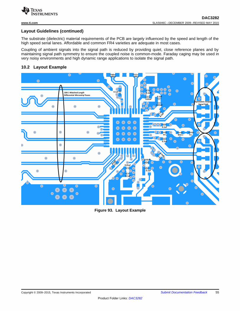
100W Matched Length
Differential Microstrip Traces
100W 100W
0.1uF
0.01uF
0.1uF
0.01uF
0.1uF
0.1uF
0.1uF
0.01uF
953W 7W
0.1uF
0W
0.1uF
0.01uF
Symmetric Output
Signal Path
DAC3282www.ti.com SLAS646C –DECEMBER 2009–REVISED MAY 2015
Layout Guidelines (continued)The substrate (dielectric) material requirements of the PCB are largely influenced by the speed and length of thehigh speed serial lanes. Affordable and common FR4 varieties are adequate in most cases.
Coupling of ambient signals into the signal path is reduced by providing quiet, close reference planes and bymaintaining signal path symmetry to ensure the coupled noise is common-mode. Faraday caging may be used invery noisy environments and high dynamic range applications to isolate the signal path.
10.2 Layout Example
Figure 93. Layout Example
Copyright © 2009–2015, Texas Instruments Incorporated Submit Documentation Feedback 55
Product Folder Links: DAC3282
DAC3282SLAS646C –DECEMBER 2009–REVISED MAY 2015 www.ti.com
11 Device and Documentation Support
11.1 Device Support
11.1.1 Definition Of Specifications
Adjacent Carrier Leakage Ratio Defined for a 3.84 Mcps 3GPP W-CDMA input signal measured in a 3.84(ACLR) MHz bandwidth at a 5MHz offset from the carrier with a 12 dB peak-to-
average ratio.Analog and Digital Power Supply Defined as the percentage error in the ratio of the delta IOUT and deltaRejection Ratio (APSSR, DPSSR) supply voltage normalized with respect to the ideal IOUT current.Differential Nonlinearity (DNL) Defined as the variation in analog output associated with an ideal 1 LSB
change in the digital input code.Gain Drift Defined as the maximum change in gain, in terms of ppm of full-scale
range (FSR) per °C, from the value at ambient (25°C) to values over thefull operating temperature range.
Gain Error Defined as the percentage error (in FSR%) for the ratio between themeasured full-scale output current and the ideal full-scale output current.
Integral Nonlinearity (INL) Defined as the maximum deviation of the actual analog output from theideal output, determined by a straight line drawn from zero scale to fullscale.
Intermodulation Distortion The two-tone IMD3 is defined as the ratio (in dBc) of the 3rd-order(IMD3, IMD) intermodulation distortion product to either fundamental output tone.Noise Spectral Density (NSD) Defined as the difference of power (in dBc) between the output tone
signal power and the noise floor of 1Hz bandwidth within the first Nyquistzone.
Offset Drift Defined as the maximum change in DC offset, in terms of ppm of full-scale range (FSR) per °C, from the value at ambient (25°C) to valuesover the full operating temperature range.
Offset Error Defined as the percentage error (in FSR%) for the ratio between themeasured mid-scale output current and the ideal mid-scale output current.
Output Compliance Range Defined as the minimum and maximum allowable voltage at the output ofthe current-output DAC. Exceeding this limit may result reduced reliabilityof the device or adversely affecting distortion performance.
Reference Voltage Drift Defined as the maximum change of the reference voltage in ppm per °Cfrom value at ambient (25°C) to values over the full operating temperaturerange.
Spurious Free Dynamic Range Defined as the difference (in dBc) between the peak amplitude of the(SFDR) output signal and the peak spurious signal.
56 Submit Documentation Feedback Copyright © 2009–2015, Texas Instruments Incorporated
Product Folder Links: DAC3282

DAC3282www.ti.com SLAS646C –DECEMBER 2009–REVISED MAY 2015
11.2 Community ResourcesThe following links connect to TI community resources. Linked contents are provided "AS IS" by the respectivecontributors. They do not constitute TI specifications and do not necessarily reflect TI's views; see TI's Terms ofUse.
TI E2E™ Online Community TI's Engineer-to-Engineer (E2E) Community. Created to foster collaborationamong engineers. At e2e.ti.com, you can ask questions, share knowledge, explore ideas and helpsolve problems with fellow engineers.
Design Support TI's Design Support Quickly find helpful E2E forums along with design support tools andcontact information for technical support.
11.3 TrademarksE2E is a trademark of Texas Instruments.All other trademarks are the property of their respective owners.
11.4 Electrostatic Discharge CautionThese devices have limited built-in ESD protection. The leads should be shorted together or the device placed in conductive foamduring storage or handling to prevent electrostatic damage to the MOS gates.
11.5 GlossarySLYZ022 — TI Glossary.
This glossary lists and explains terms, acronyms, and definitions.
12 Mechanical, Packaging, and Orderable InformationThe following pages include mechanical, packaging, and orderable information. This information is the mostcurrent data available for the designated devices. This data is subject to change without notice and revision ofthis document. For browser-based versions of this data sheet, refer to the left-hand navigation.
Copyright © 2009–2015, Texas Instruments Incorporated Submit Documentation Feedback 57
Product Folder Links: DAC3282
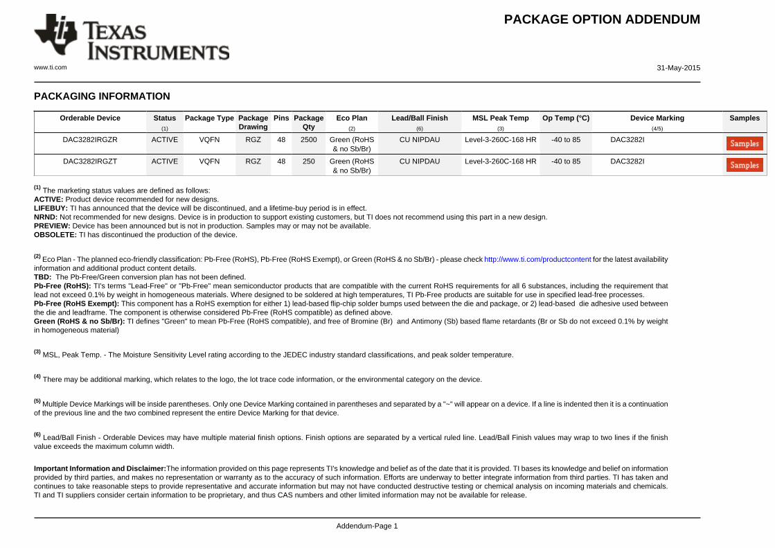
PACKAGE OPTION ADDENDUM
www.ti.com 31-May-2015
Addendum-Page 1
PACKAGING INFORMATION
Orderable Device Status(1)
Package Type PackageDrawing
Pins PackageQty
Eco Plan(2)
Lead/Ball Finish(6)
MSL Peak Temp(3)
Op Temp (°C) Device Marking(4/5)
Samples
DAC3282IRGZR ACTIVE VQFN RGZ 48 2500 Green (RoHS& no Sb/Br)
CU NIPDAU Level-3-260C-168 HR -40 to 85 DAC3282I
DAC3282IRGZT ACTIVE VQFN RGZ 48 250 Green (RoHS& no Sb/Br)
CU NIPDAU Level-3-260C-168 HR -40 to 85 DAC3282I
(1) The marketing status values are defined as follows:ACTIVE: Product device recommended for new designs.LIFEBUY: TI has announced that the device will be discontinued, and a lifetime-buy period is in effect.NRND: Not recommended for new designs. Device is in production to support existing customers, but TI does not recommend using this part in a new design.PREVIEW: Device has been announced but is not in production. Samples may or may not be available.OBSOLETE: TI has discontinued the production of the device.
(2) Eco Plan - The planned eco-friendly classification: Pb-Free (RoHS), Pb-Free (RoHS Exempt), or Green (RoHS & no Sb/Br) - please check http://www.ti.com/productcontent for the latest availabilityinformation and additional product content details.TBD: The Pb-Free/Green conversion plan has not been defined.Pb-Free (RoHS): TI's terms "Lead-Free" or "Pb-Free" mean semiconductor products that are compatible with the current RoHS requirements for all 6 substances, including the requirement thatlead not exceed 0.1% by weight in homogeneous materials. Where designed to be soldered at high temperatures, TI Pb-Free products are suitable for use in specified lead-free processes.Pb-Free (RoHS Exempt): This component has a RoHS exemption for either 1) lead-based flip-chip solder bumps used between the die and package, or 2) lead-based die adhesive used betweenthe die and leadframe. The component is otherwise considered Pb-Free (RoHS compatible) as defined above.Green (RoHS & no Sb/Br): TI defines "Green" to mean Pb-Free (RoHS compatible), and free of Bromine (Br) and Antimony (Sb) based flame retardants (Br or Sb do not exceed 0.1% by weightin homogeneous material)
(3) MSL, Peak Temp. - The Moisture Sensitivity Level rating according to the JEDEC industry standard classifications, and peak solder temperature.
(4) There may be additional marking, which relates to the logo, the lot trace code information, or the environmental category on the device.
(5) Multiple Device Markings will be inside parentheses. Only one Device Marking contained in parentheses and separated by a "~" will appear on a device. If a line is indented then it is a continuationof the previous line and the two combined represent the entire Device Marking for that device.
(6) Lead/Ball Finish - Orderable Devices may have multiple material finish options. Finish options are separated by a vertical ruled line. Lead/Ball Finish values may wrap to two lines if the finishvalue exceeds the maximum column width.
Important Information and Disclaimer:The information provided on this page represents TI's knowledge and belief as of the date that it is provided. TI bases its knowledge and belief on informationprovided by third parties, and makes no representation or warranty as to the accuracy of such information. Efforts are underway to better integrate information from third parties. TI has taken andcontinues to take reasonable steps to provide representative and accurate information but may not have conducted destructive testing or chemical analysis on incoming materials and chemicals.TI and TI suppliers consider certain information to be proprietary, and thus CAS numbers and other limited information may not be available for release.
PACKAGE OPTION ADDENDUM
www.ti.com 31-May-2015
Addendum-Page 2
In no event shall TI's liability arising out of such information exceed the total purchase price of the TI part(s) at issue in this document sold by TI to Customer on an annual basis.

TAPE AND REEL INFORMATION
*All dimensions are nominal
Device PackageType
PackageDrawing
Pins SPQ ReelDiameter
(mm)
ReelWidth
W1 (mm)
A0(mm)
B0(mm)
K0(mm)
P1(mm)
W(mm)
Pin1Quadrant
DAC3282IRGZR VQFN RGZ 48 2500 330.0 16.4 7.3 7.3 1.5 12.0 16.0 Q2
DAC3282IRGZT VQFN RGZ 48 250 180.0 16.4 7.3 7.3 1.5 12.0 16.0 Q2
PACKAGE MATERIALS INFORMATION
www.ti.com 3-Aug-2017
Pack Materials-Page 1
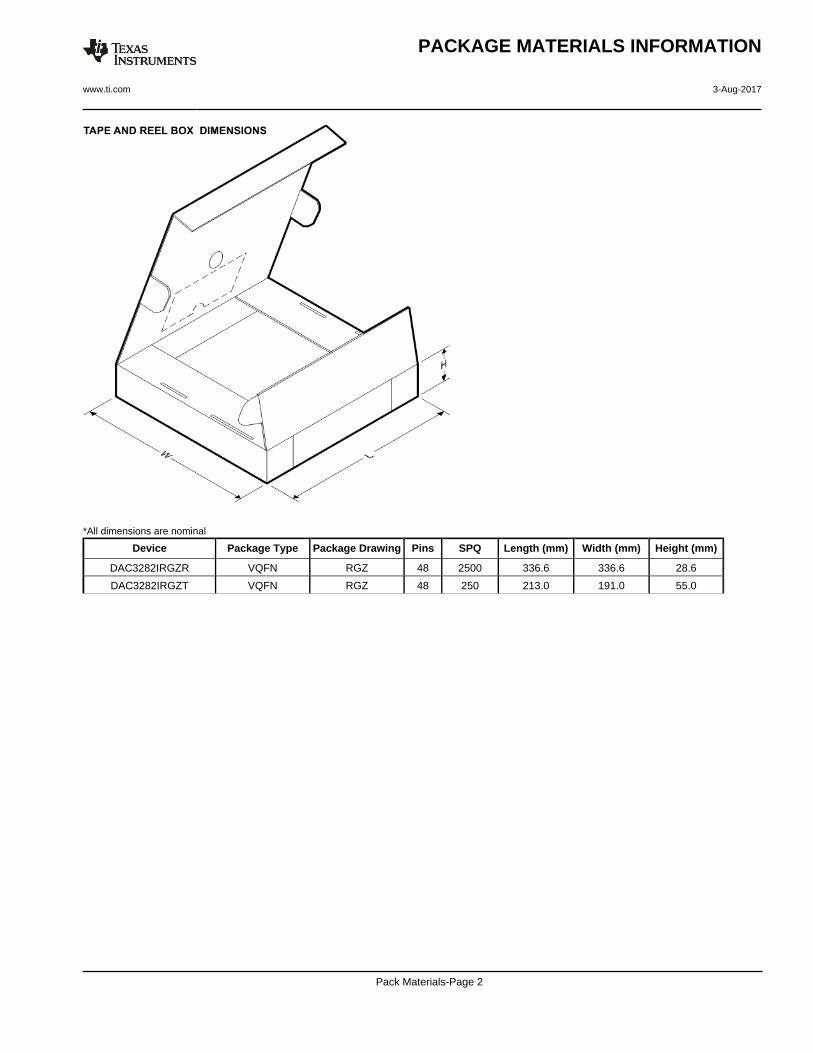
*All dimensions are nominal
Device Package Type Package Drawing Pins SPQ Length (mm) Width (mm) Height (mm)
DAC3282IRGZR VQFN RGZ 48 2500 336.6 336.6 28.6
DAC3282IRGZT VQFN RGZ 48 250 213.0 191.0 55.0
PACKAGE MATERIALS INFORMATION
www.ti.com 3-Aug-2017
Pack Materials-Page 2


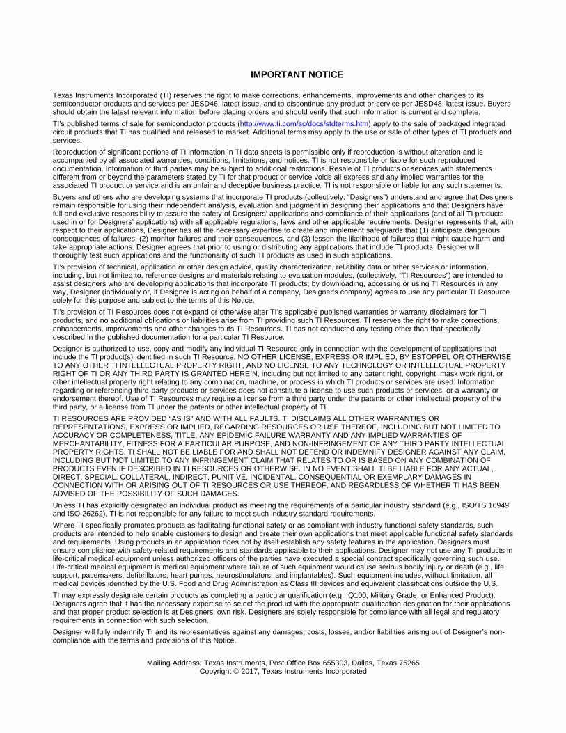
IMPORTANT NOTICE
Texas Instruments Incorporated (TI) reserves the right to make corrections, enhancements, improvements and other changes to itssemiconductor products and services per JESD46, latest issue, and to discontinue any product or service per JESD48, latest issue. Buyersshould obtain the latest relevant information before placing orders and should verify that such information is current and complete.TI’s published terms of sale for semiconductor products (http://www.ti.com/sc/docs/stdterms.htm) apply to the sale of packaged integratedcircuit products that TI has qualified and released to market. Additional terms may apply to the use or sale of other types of TI products andservices.Reproduction of significant portions of TI information in TI data sheets is permissible only if reproduction is without alteration and isaccompanied by all associated warranties, conditions, limitations, and notices. TI is not responsible or liable for such reproduceddocumentation. Information of third parties may be subject to additional restrictions. Resale of TI products or services with statementsdifferent from or beyond the parameters stated by TI for that product or service voids all express and any implied warranties for theassociated TI product or service and is an unfair and deceptive business practice. TI is not responsible or liable for any such statements.Buyers and others who are developing systems that incorporate TI products (collectively, “Designers”) understand and agree that Designersremain responsible for using their independent analysis, evaluation and judgment in designing their applications and that Designers havefull and exclusive responsibility to assure the safety of Designers' applications and compliance of their applications (and of all TI productsused in or for Designers’ applications) with all applicable regulations, laws and other applicable requirements. Designer represents that, withrespect to their applications, Designer has all the necessary expertise to create and implement safeguards that (1) anticipate dangerousconsequences of failures, (2) monitor failures and their consequences, and (3) lessen the likelihood of failures that might cause harm andtake appropriate actions. Designer agrees that prior to using or distributing any applications that include TI products, Designer willthoroughly test such applications and the functionality of such TI products as used in such applications.TI’s provision of technical, application or other design advice, quality characterization, reliability data or other services or information,including, but not limited to, reference designs and materials relating to evaluation modules, (collectively, “TI Resources”) are intended toassist designers who are developing applications that incorporate TI products; by downloading, accessing or using TI Resources in anyway, Designer (individually or, if Designer is acting on behalf of a company, Designer’s company) agrees to use any particular TI Resourcesolely for this purpose and subject to the terms of this Notice.TI’s provision of TI Resources does not expand or otherwise alter TI’s applicable published warranties or warranty disclaimers for TIproducts, and no additional obligations or liabilities arise from TI providing such TI Resources. TI reserves the right to make corrections,enhancements, improvements and other changes to its TI Resources. TI has not conducted any testing other than that specificallydescribed in the published documentation for a particular TI Resource.Designer is authorized to use, copy and modify any individual TI Resource only in connection with the development of applications thatinclude the TI product(s) identified in such TI Resource. NO OTHER LICENSE, EXPRESS OR IMPLIED, BY ESTOPPEL OR OTHERWISETO ANY OTHER TI INTELLECTUAL PROPERTY RIGHT, AND NO LICENSE TO ANY TECHNOLOGY OR INTELLECTUAL PROPERTYRIGHT OF TI OR ANY THIRD PARTY IS GRANTED HEREIN, including but not limited to any patent right, copyright, mask work right, orother intellectual property right relating to any combination, machine, or process in which TI products or services are used. Informationregarding or referencing third-party products or services does not constitute a license to use such products or services, or a warranty orendorsement thereof. Use of TI Resources may require a license from a third party under the patents or other intellectual property of thethird party, or a license from TI under the patents or other intellectual property of TI.TI RESOURCES ARE PROVIDED “AS IS” AND WITH ALL FAULTS. TI DISCLAIMS ALL OTHER WARRANTIES ORREPRESENTATIONS, EXPRESS OR IMPLIED, REGARDING RESOURCES OR USE THEREOF, INCLUDING BUT NOT LIMITED TOACCURACY OR COMPLETENESS, TITLE, ANY EPIDEMIC FAILURE WARRANTY AND ANY IMPLIED WARRANTIES OFMERCHANTABILITY, FITNESS FOR A PARTICULAR PURPOSE, AND NON-INFRINGEMENT OF ANY THIRD PARTY INTELLECTUALPROPERTY RIGHTS. TI SHALL NOT BE LIABLE FOR AND SHALL NOT DEFEND OR INDEMNIFY DESIGNER AGAINST ANY CLAIM,INCLUDING BUT NOT LIMITED TO ANY INFRINGEMENT CLAIM THAT RELATES TO OR IS BASED ON ANY COMBINATION OFPRODUCTS EVEN IF DESCRIBED IN TI RESOURCES OR OTHERWISE. IN NO EVENT SHALL TI BE LIABLE FOR ANY ACTUAL,DIRECT, SPECIAL, COLLATERAL, INDIRECT, PUNITIVE, INCIDENTAL, CONSEQUENTIAL OR EXEMPLARY DAMAGES INCONNECTION WITH OR ARISING OUT OF TI RESOURCES OR USE THEREOF, AND REGARDLESS OF WHETHER TI HAS BEENADVISED OF THE POSSIBILITY OF SUCH DAMAGES.Unless TI has explicitly designated an individual product as meeting the requirements of a particular industry standard (e.g., ISO/TS 16949and ISO 26262), TI is not responsible for any failure to meet such industry standard requirements.Where TI specifically promotes products as facilitating functional safety or as compliant with industry functional safety standards, suchproducts are intended to help enable customers to design and create their own applications that meet applicable functional safety standardsand requirements. Using products in an application does not by itself establish any safety features in the application. Designers mustensure compliance with safety-related requirements and standards applicable to their applications. Designer may not use any TI products inlife-critical medical equipment unless authorized officers of the parties have executed a special contract specifically governing such use.Life-critical medical equipment is medical equipment where failure of such equipment would cause serious bodily injury or death (e.g., lifesupport, pacemakers, defibrillators, heart pumps, neurostimulators, and implantables). Such equipment includes, without limitation, allmedical devices identified by the U.S. Food and Drug Administration as Class III devices and equivalent classifications outside the U.S.TI may expressly designate certain products as completing a particular qualification (e.g., Q100, Military Grade, or Enhanced Product).Designers agree that it has the necessary expertise to select the product with the appropriate qualification designation for their applicationsand that proper product selection is at Designers’ own risk. Designers are solely responsible for compliance with all legal and regulatoryrequirements in connection with such selection.Designer will fully indemnify TI and its representatives against any damages, costs, losses, and/or liabilities arising out of Designer’s non-compliance with the terms and provisions of this Notice.
Mailing Address: Texas Instruments, Post Office Box 655303, Dallas, Texas 75265Copyright © 2017, Texas Instruments Incorporated