16-bit, 8-channel simultaneous sampling data acquisition ... · 16-bit, 8-channel simultaneous...
TRANSCRIPT

16-Bit, 8-Channel Simultaneous Sampling Data Acquisition System
Data Sheet ADAS3023
Rev. B Document Feedback Information furnished by Analog Devices is believed to be accurate and reliable. However, no responsibility is assumed by Analog Devices for its use, nor for any infringements of patents or other rights of third parties that may result from its use. Specifications subject to change without notice. No license is granted by implication or otherwise under any patent or patent rights of Analog Devices. Trademarks and registered trademarks are the property of their respective owners.
One Technology Way, P.O. Box 9106, Norwood, MA 02062-9106, U.S.A. Tel: 781.329.4700 ©2013–2017 Analog Devices, Inc. All rights reserved. Technical Support www.analog.com
FEATURES Ease of use, 16-bit complete data acquisition system Simultaneous sampling selection of 2, 4, 6, and 8 channels Differential input voltage range: ±20.48 V maximum High impedance 8-channel input: >500 MΩ High input common-mode rejection: 95.0 dB User-programmable input ranges On-chip 4.096 V reference and buffer No latency/pipeline delay (SAR architecture) Serial 4-wire 1.8 V to 5 V SPI-/SPORT-compatible interface 40-lead LFCSP package (6 mm × 6 mm): −40°C to +85°C
APPLICATIONS Multichannel data acquisition and system monitoring Process control Power line monitoring Automated test equipment Patient monitoring Spectrum analysis Instrumentation
FUNCTIONAL BLOCK DIAGRAM
BUF
REF
LOGIC/INTERFACE
TRACKAND
HOLDPGIA PulSAR
ADC
DIFF TOCOM
IN0
CNV
CS
SCK
DIN
SDO
REFIN
IN1IN2IN3IN4IN5IN6IN7
COM
VDDH AVDD DVDD VIO RESET
REF1/REF2DGNDAGNDVSSH
PD
ADAS3023
1094
2-00
1
BUSY/SDO2
Figure 1.
GENERAL DESCRIPTION The ADAS3023 is a complete 16-bit, successive approximation-based, analog-to-digital data acquisition system. This device is capable of simultaneously sampling up to 500 kSPS for two channels, 250 kSPS for four channels, 167 kSPS for six chan-nels, and 125 kSPS for eight channels, and manufactured on the Analog Devices, Inc., proprietary iCMOS® high voltage industrial process technology.
The ADAS3023 integrates eight channels of low leakage track-and-hold design, a programmable gain instrumentation amplifier (PGIA) stage with a high common-mode rejection offering four differential input ranges, a precision low drift 4.096 V reference and buffer, and a 16-bit charge redistribution PulSAR® successive approximation register (SAR) analog-to-digital converter (ADC). The ADAS3023 is factory calibrated and can resolve differential input ranges of up to ±20.48 V when using ±15 V supplies.
The ADAS3023 simplifies design challenges by eliminating signal buffering, level shifting, amplification and attenuation, common-mode rejection, settling time, or any of the other analog signal conditioning challenges, and allows smaller form factor, faster time to market, and lower costs.
The ADAS3023 is available in a 40-lead LFCSP with operation specified from −40°C to +85°C.
Table 1. Typical Input Range Selection Single-Ended Signals1 Input Range, VIN 0 V to 1 V ±1.28 V 0 V to 2.5 V ±2.56 V 0 V to 5 V ±5.12 V 0 V to 10 V ±10.24 V 1 See Figure 39 and Figure 40 in the Analog Inputs section for more
information.

ADAS3023 Data Sheet
Rev. B | Page 2 of 30
TABLE OF CONTENTS Features .............................................................................................. 1
Applications ....................................................................................... 1
Functional Block Diagram .............................................................. 1
General Description ......................................................................... 1
Revision History ............................................................................... 2
Specifications ..................................................................................... 3
Timing Specifications .................................................................. 6
Timing Diagrams .......................................................................... 8
Absolute Maximum Ratings ....................................................... 9
Thermal Resistance ...................................................................... 9
ESD Caution .................................................................................. 9
Pin Configurations and Function Descriptions ......................... 10
Typical Performance Characteristics ........................................... 12
Terminology .................................................................................... 17
Theory of Operation ...................................................................... 19
Overview ...................................................................................... 19
Operation ..................................................................................... 19
Transfer Functions ..................................................................... 20
Typical Application Connection Diagram .............................. 21
Analog Inputs.............................................................................. 21
Voltage Reference Input/Output .............................................. 22
Power Supply ............................................................................... 24
Power Dissipation Modes .......................................................... 25
Conversion Modes ..................................................................... 25
Digital Interface .............................................................................. 26
Conversion Control ................................................................... 26
RESET and Power-Down (PD) Inputs .................................... 26
Serial Data Interface ................................................................... 27
General Timing........................................................................... 28
Configuration Register .............................................................. 29
Packaging and Ordering Information ......................................... 30
Outline Dimensions ................................................................... 30
Ordering Guide .......................................................................... 30
REVISION HISTORY 10/2017—Rev. A to Rev. B Changed REFx to REF1/REF2 ..................................... Throughout Changes to General Description Section ...................................... 1 Changes to Table 2 ............................................................................ 3 Changes to Table 3 ....................................................................................... 6 Changes to Figure 5 .......................................................................... 8 Added Thermal Resistance Section and Table 5; Renumbered Sequentially ....................................................................................... 9 Changes to Table 4 ....................................................................................... 9 Changes to Figure 6 Caption and Table 6 Title .......................... 10 Change to Figure 35 ....................................................................... 19 Changes to Theory of Operation Section .................................... 19 Change to Figure 38 ....................................................................... 21 Added Alternate Sequence Section .............................................. 24 Change to Core Supplies Section .................................................. 24 Changes to Figure 46 ...................................................................... 24 Changes to Serial Data Interface Section .................................... 27 Changes to Figure 50 ...................................................................... 28 Changes to Table 12 ........................................................................ 29 Updated Outline Dimensions ....................................................... 30 Changes to Ordering Guide .......................................................... 30
2/2014—Rev. 0 to Rev. A Changes to Table 2 ............................................................................. 5 Changes to Figure 38 ...................................................................... 21 5/2013—Revision 0: Initial Version

Data Sheet ADAS3023
Rev. B | Page 3 of 30
SPECIFICATIONS VDDH = 15 V ± 5%, VSSH = −15V ± 5%, AVDD = DVDD = 5 V ± 5%; VIO = 1.8 V to AVDD, internal reference VREF = 4.096 V, fS = 500 kSPS, all specifications TMIN to TMAX, unless otherwise noted.
Table 2. Parameter Test Conditions/Comments Min Typ Max Unit1 RESOLUTION 16 Bits ANALOG INPUT (IN0 to IN7, COM)
Input Impedance ZIN 500 MΩ Operating Input Voltage Range2 VIN, on any single pin VSSH + 2.5 VDDH − 2.5 V Differential Input Voltage Ranges, VIN VINX − COM PGIA gain = 0.2, VIN = 40.96 V p-p −5 VREF +5 VREF V PGIA gain = 0.4, VIN = 20.48 V p-p −2.5 VREF +2.5 VREF V PGIA gain = 0.8, VIN = 10.24 V p-p −1.25 VREF +1.25 VREF V PGIA gain = 1.6, VIN = 5.12 V p-p −0.625 VREF +0.625 VREF V
THROUGHPUT Conversion Rate Two channels 0 500 kSPS
Four channels 0 250 kSPS Six channels 0 167 kSPS Eight channels 0 125 kSPS Transient Response3 Full-scale step 820 ns
DC ACCURACY No Missing Codes 16 Bits Integral Linearity Error PGIA gain = 0.2, 0.4, or 0.8, COM = 0 V −2.5 ±1 +2.5 LSB PGIA gain = 1.6, COM = 0 V −3 ±1 +3 Differential Linearity Error All PGIA gains, COM = 0 V −0.95 ±0.5 +1.25 LSB Transition Noise PGIA gain = 0.2 or 0.4 6 LSB PGIA gain = 0.8 7 LSB PGIA gain = 1.6 10 LSB
Gain Error4 External reference, all PGIA gains −0.075 +0.075 %FS Gain Error Match, Delta Mean External reference, all PGIA gains −0.05 +0.05 %FS Gain Error Temperature Drift External reference, PGIA gain = 0.2, 0.4, or 0.8 1 ppm/°C External reference, PGIA gain = 1.6 2 ppm/°C Offset Error External reference, PGIA gain = 0.2 −65 −35 +65 LSB External reference, PGIA gain = 0.4 −85 −45 +12 LSB External reference, PGIA gain = 0.8 −10 0 +10 LSB External reference, PGIA gain = 1.6 0 130 250 LSB Offset Error Match, Delta Mean External reference, PGIA gain = 0.2, 0.4, 0.8, or 1.6 −15 ±1 +15 LSB Offset Error Temperature Drift External reference, PGIA gain = 0.2 or 0.4, IN0 to IN7 0 0.5 2 ppm/°C External reference, PGIA gain = 0.8, IN0 to IN7 0 1.5 3 ppm/°C External reference, PGIA gain = 1.6, IN0 to IN7 0 2.5 5 ppm/°C
AC ACCURACY5 Internal reference Signal-to-Noise Ratio (SNR) fIN = 1 kHz, COM = 0 V PGIA gain = 0.2 90.0 91.5 dB PGIA gain = 0.4 89.5 91.0 dB PGIA gain = 0.8 87.5 89.0 dB PGIA gain = 1.6 85.0 86.5 dB

ADAS3023 Data Sheet
Rev. B | Page 4 of 30
Parameter Test Conditions/Comments Min Typ Max Unit1 Signal-to-Noise + Distortion (SINAD) fIN = 1 kHz; two, four, six, and eight channels PGIA gain = 0.2 89.5 91.0 dB PGIA gain = 0.4 89.0 90.5 dB PGIA gain = 0.8 87.0 88.5 dB PGIA gain = 1.6 84.0 86.0 dB Dynamic Range fIN = 1 kHz, −60 dB input PGIA gain = 0.2 91.0 92.0 dB PGIA gain = 0.4 90.5 91.5 dB PGIA gain = 0.8 88.0 89.5 dB PGIA gain = 1.6 86.0 87.0 dB Total Harmonic Distortion (THD) fIN = 1 kHz, all PGIA gains −100 dB Spurious-Free Dynamic Range (SFDR) fIN = 1 kHz, all PGIA gains 105 dB Channel-to-Channel Crosstalk fIN = 1 kHz, all channels inactive 95.0 dB DC Common-Mode Rejection Ratio
(CMRR) All channels, all PGIA gains 95.0 dB
−3 dB Input Bandwidth −40 dBFS 8 MHz INTERNAL REFERENCE
REF1/REF2 Pins Output Voltage TA = 25°C 4.088 4.096 4.104 V Output Current TA = 25°C 250 µA Temperature Drift REFEN bit = 1 ±5 ppm/°C REFEN bit = 0, REFIN pin = 2.5 V ±1 ppm/°C
Line Regulation Internal Reference AVDD = 5 V ± 5% 20 μV/V Buffer Only AVDD = 5 V ± 5% 4 ppm
REFIN Output Voltage6 TA = 25°C 2.495 2.5 2.505 V Turn-On Settling Time CREFIN, CREF1, CREF2 = 10 µF||0.1 µF 100 ms
EXTERNAL REFERENCE REFEN bit = 0 Voltage Range REF1/REF2 input, REFIN = 0 V 4.000 4.096 4.104 V REFIN input (buffered) 2.5 2.505 V Current Drain fS = 500 kSPS 100 µA
DIGITAL INPUTS Logic Levels
Input Voltage High, VIH VIO > 3 V 0.7 × VIO VIO + 0.3 V VIO ≤ 3 V 0.9 × VIO VIO + 0.3 V
Input Voltage Low, VIL VIO > 3 V −0.3 +0.3 × VIO V VIO ≤ 3 V −0.3 +0.1 × VIO V
Input Current High, IIH −1 +1 µA Input Current Low, IIL −1 +1 µA
DIGITAL OUTPUTS7 Data Format Twos complement Low Voltage Output, VOL ISINK = +500 µA 0.4 V High Voltage Output, VOH ISOURCE = −500 µA VIO − 0.3 V
POWER SUPPLIES VIO 1.8 AVDD + 0.3 V AVDD 4.75 5 5.25 V DVDD 4.75 5 5.25 V VDDH VDDH > input voltage + 2.5 V 14.25 15 15.75 V VSSH VSSH < input voltage − 2.5 V −15.75 −15 −14.25 V

Data Sheet ADAS3023
Rev. B | Page 5 of 30
Parameter Test Conditions/Comments Min Typ Max Unit1 IVDDH Two channels 5.0 5.5 mA Four channels 6.0 7.0 mA Six channels 9.5 10.5 mA Eight channels 9.5 10.5 mA PD = 1 10.0 µA IVSSH Two channels −5.5 −5.0 mA Four channels −6.5 −5.5 mA Six channels −10.0 −8.5 mA Eight channels −10.0 −8.5 mA All PGIA gains, PD = 1 10.0 µA IAVDD All PGIA gains, PD = 0, reference buffer enabled 16.0 17.0 mA All PGIA gains, PD = 0, reference buffer disabled 15.5 mA All PGIA gains, PD = 1 100 µA IDVDD All PGIA gains, PD = 0 2.5 3 mA All PGIA gains, PD = 1 100 µA IVIO All PGIA gains, PD = 0, VIO = 3.3 V 1.0 mA All PGIA gains, PD = 1 10.0 µA Power Supply Sensitivity External reference, TA = 25°C PGIA gain = 0.2 or 0.4, VDDH and VSSH = ±15 V ±
5% ±0.1 LSB
PGIA gain = 0.8, VDDH and VSSH = ±15 V ± 5% ±0.2 LSB PGIA gain = 1.6, VDDH and VSSH = ±15 V ± 5% ±0.4 LSB PGIA gain = 0.2 or 0.4, AVDD and DVDD = ±5 V ± 5% ±1.0 LSB PGIA gain = 0.8, AVDD and DVDD = ±5 V ± 5% ±1.5 LSB PGIA gain = 1.6, AVDD and DVDD = ±5 V ± 5% ±2.5 LSB
TEMPERATURE RANGE Specified Performance TMIN to TMAX −40 +85 °C
1 The LSB unit means least significant bit. The weight of the LSB, referred to input, changes depending on the input voltage range. See the Programmable Gain section
for the LSB size. 2 Full-scale differential input ranges of ±2.56 V, ±5.12 V, ±10.24 V, and ±20.48 V are set by the configuration register. 3 If using the external multiplexer in front of the ADAS3023, it must be switched at least 820 ns prior to the rising edge of CNV. 4 See the Terminology section. These parameters are specified at ambient temperature with an external reference. All other influences of temperature and supply are
measured and specified separately. 5 All ac specifications expressed in decibels are referenced to the full-scale input range (FSR) and are tested with an input signal at 0.5 dB below full scale, unless
otherwise specified. 6 REFIN output voltage is the output from the internal band gap reference. 7 There is no pipeline delay. Conversion results are available immediately after a conversion is completed.
ADAS3023 Data Sheet
Rev. B | Page 6 of 30
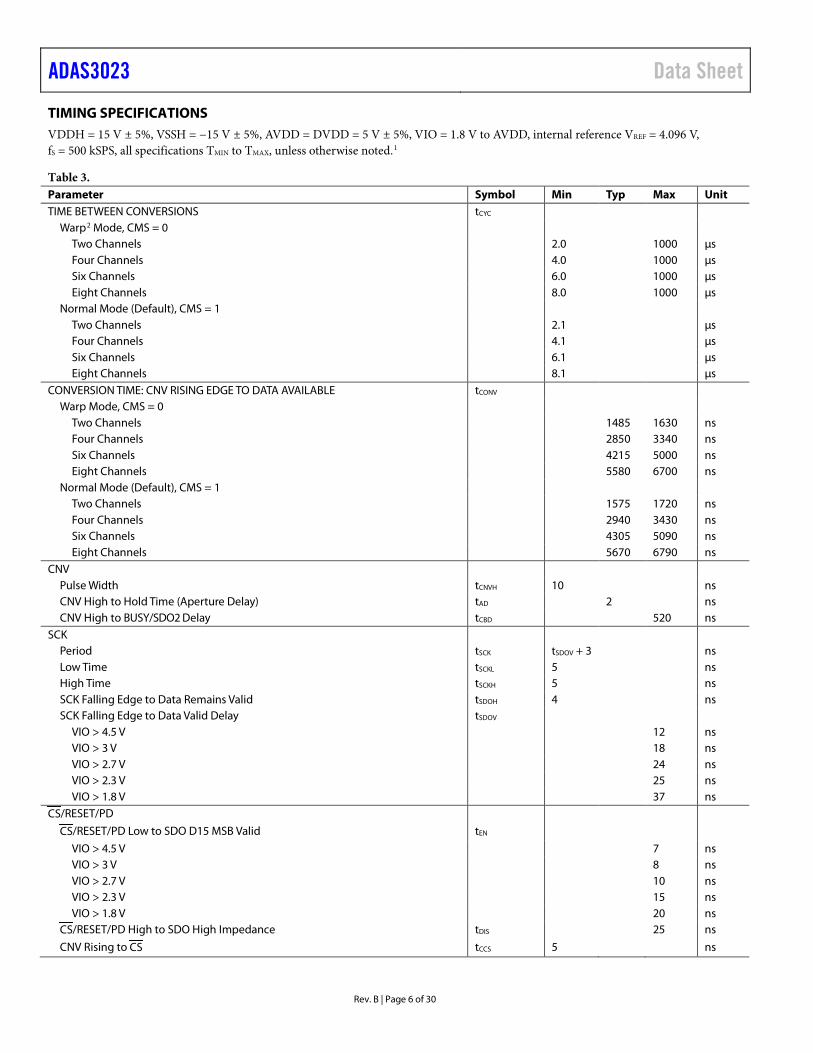
TIMING SPECIFICATIONS VDDH = 15 V ± 5%, VSSH = −15 V ± 5%, AVDD = DVDD = 5 V ± 5%, VIO = 1.8 V to AVDD, internal reference VREF = 4.096 V, fS = 500 kSPS, all specifications TMIN to TMAX, unless otherwise noted.1
Table 3. Parameter Symbol Min Typ Max Unit TIME BETWEEN CONVERSIONS tCYC
Warp2 Mode, CMS = 0 Two Channels 2.0 1000 µs Four Channels 4.0 1000 µs Six Channels 6.0 1000 µs Eight Channels 8.0 1000 µs
Normal Mode (Default), CMS = 1 Two Channels 2.1 µs Four Channels 4.1 µs Six Channels 6.1 µs Eight Channels 8.1 µs
CONVERSION TIME: CNV RISING EDGE TO DATA AVAILABLE tCONV Warp Mode, CMS = 0
Two Channels 1485 1630 ns Four Channels 2850 3340 ns Six Channels 4215 5000 ns Eight Channels 5580 6700 ns
Normal Mode (Default), CMS = 1 Two Channels 1575 1720 ns Four Channels 2940 3430 ns Six Channels 4305 5090 ns Eight Channels 5670 6790 ns
CNV Pulse Width tCNVH 10 ns CNV High to Hold Time (Aperture Delay) tAD 2 ns CNV High to BUSY/SDO2 Delay tCBD 520 ns
SCK Period tSCK tSDOV + 3 ns Low Time tSCKL 5 ns High Time tSCKH 5 ns SCK Falling Edge to Data Remains Valid tSDOH 4 ns SCK Falling Edge to Data Valid Delay tSDOV
VIO > 4.5 V 12 ns VIO > 3 V 18 ns VIO > 2.7 V 24 ns VIO > 2.3 V 25 ns VIO > 1.8 V 37 ns
CS/RESET/PD
CS/RESET/PD Low to SDO D15 MSB Valid tEN
VIO > 4.5 V 7 ns VIO > 3 V 8 ns VIO > 2.7 V 10 ns VIO > 2.3 V 15 ns VIO > 1.8 V 20 ns
CS/RESET/PD High to SDO High Impedance tDIS 25 ns
CNV Rising to CS tCCS 5 ns

Data Sheet ADAS3023
Rev. B | Page 7 of 30
Parameter Symbol Min Typ Max Unit DIN
DIN Valid Setup Time from SCK Rising Edge tDINS 4 ns DIN Valid Hold Time from SCK Falling Edge tDINH 4 ns
RESET/PD HIGH PULSE tRH 5 ns 1 See Figure 2 and Figure 3 for load conditions. 2 Exceeding the maximum time has an effect on the accuracy of the conversion (see the Conversion Modes section).
Circuit and Voltage Diagrams
IOL
500µA
500µA
IOH
1.4VTO SDOCL
50pF
1094
2-00
2
Figure 2. Load Circuit for Digital Interface Timing
30% VIO70% VIO
2V OR VIO – 0.5V1
0.8V OR 0.5V20.8V OR 0.5V22V OR VIO – 0.5V1
tDELAY tDELAY
12V IF VIO > 2.5V; VIO – 0.5V IF VIO < 2.5V.20.8V IF VIO > 2.5V; 0.5V IF VIO < 2.5V. 10
942-
003
Figure 3. Voltage Levels for Timing

ADAS3023 Data Sheet
Rev. B | Page 8 of 30
TIMING DIAGRAMS
1 16 1 16 1 16 1 16 1 16 1 16
PHASE
SCK
DIN
SDO
BUSY/SDO2
SOC SOC
EOC
NOTE 2NOTE 1
NOTE 4
NOTE 3
NOTE 2
NOTE 1
EOCPOWER
UPCONV
CYC
CNVH
CBD
AD
CONVERSION (n) CONVERSION (n + 1)ACQUISITION (n + 1) ACQUISITION (n + 2)
SOC
DATA (n)
CFG (n + 2) CFG (n + 3)
CH0 CH1 CH7 CH0 CH1 CH7
DATA (n + 1)
1094
2-00
4
NOTES1. DATA ACCESS CAN ONLY OCCUR AFTER CONVERSION. BOTH CONVERSION RESULT AND THE CFG REGISTER ARE UPDATED AT THE END OF THE CONVERSION (EOC).2. A TOTAL OF 16 SCK FALLING EDGES ARE REQUIRED FOR CONVERSION RESULT. AN ADDITIONAL 16 EDGES AFTER THE LAST CONVERSION RESULT ON BUSY READS BACK THE CFG ASSOCIATED WITH CONVERSION.3. CS CAN BE HELD LOW OR CONNECTED TO CNV. CS IS SHOWN WITH FULL INDEPENDENT CONTROL.4. FOR OPTIMAL PERFORMANCE, DATA ACCESS MUST NOT OCCUR DURING THE SAMPLING INSTANT. A MINIMUM TIME OF AT LEAST THE APERATURE DELAY, tAD, MUST LAPSE PRIOR TO DATA ACCESS.
Figure 4. General Timing Diagram with BUSY/SDO2 Disabled
1 16
PHASE
CNV
SCK
DIN
SDO
CS
SOC SOC
EOC
NOTE 1
NOTE 4
NOTE 3
NOTE 2
NOTE 1
EOCPOWER
UPtCONV
tCYC
tCNVH
tAD
CONVERSION (n) CONVERSION (n + 1)ACQUISITION (n + 1) ACQUISITION (n + 2)
SOC
DATA (n)
CFG (n + 2) CFG (n + 3)
DATA (n + 1)
CH0 CH1 CH2 CH3 CH0 CH1 CH2 CH3
1 16 1 16 1 16 1 16 1 16 1 16 1 16
1094
2-00
5
NOTES1. DATA ACCESS CAN ONLY OCCUR AFTER CONVERSION. BOTH CONVERSION RESULT AND THE CFG REGISTER ARE UPDATED AT THE END OF THE CONVERSION (EOC).2. A TOTAL OF 16 SCK FALLING EDGES ARE REQUIRED FOR CONVERSION RESULT. AN ADDITIONAL 16 EDGES AFTER THE LAST CONVERSION RESULT ON BUSY READS BACK THE CFG ASSOCIATED WITH CONVERSION.3. CS CAN BE HELD LOW OR CONNECTED TO CNV. CS IS SHOWN WITH FULL INDEPENDENT CONTROL.4. FOR OPTIMAL PERFORMANCE, DATA ACCESS MUST NOT OCCUR DURING THE SAMPLING INSTANT. A MINIMUM TIME OF AT LEAST THE APERATURE DELAY, tAD, MUST LAPSE PRIOR TO DATA ACCESS.
BUSY/SDO2
CBDCH4 CH5 CH6 CH7 CH4 CH5 CH6 CH7
Figure 5. General Timing Diagram with BUSY/SDO2 Enabled
Data Sheet ADAS3023
Rev. B | Page 9 of 30
ABSOLUTE MAXIMUM RATINGS
Table 4. Parameter Rating Analog Inputs/Outputs
INx, COM to AGND VSSH − 0.3 V to VDDH + 0.3 V REF1/REF2 to AGND AGND − 0.3 V to AVDD + 0.3 V REFIN to AGND AGND − 0.3 V to +2.7 V REFN to AGND ±0.3 V
Ground Voltage Differences AGND, RGND, DGND ±0.3 V
Supply Voltages VDDH to AGND −0.3 V to +16.5 V VSSH to AGND +0.3 V to −16.5 V AVDD, DVDD, VIO to AGND −0.3 V to +7 V ACAP, DCAP, RCAP to AGND −0.3 V to +2.7 V
Digital Inputs/Outputs CNV, DIN, SCK, RESET, PD, CS
to DGND −0.3 V to VIO + 0.3 V
SDO, BUSY/SDO2 to DGND −0.3 V to VIO + 0.3 V Internal Power Dissipation 2 W Junction Temperature 150°C Storage Temperature Range −65°C to +150°C
Stresses at or above those listed under Absolute Maximum Ratings may cause permanent damage to the product. This is a stress rating only; functional operation of the product at these or any other conditions above those indicated in the operational section of this specification is not implied. Operation beyond the maximum operating conditions for extended periods may affect product reliability.
THERMAL RESISTANCE Thermal performance is directly linked to printed circuit board (PCB) design and operating environment. Close attention to PCB thermal design is required.
Table 5. Thermal Resistance Package Type θJA θJC Unit CP-40-15 44.1 0.28 °C/W
ESD CAUTION

ADAS3023 Data Sheet
Rev. B | Page 10 of 30
PIN CONFIGURATION AND FUNCTION DESCRIPTIONS
1IN02IN13IN24IN35AGND6IN47IN58IN69IN7
10COM
23 AGND24 AGND25 DCAP26 ACAP27 DVDD28 AVDD29 AGND30 AGND
22 DGND21 DGND
11S
C21
NID
31TESE
R
51DP
71OI V
61K
CS
81O
DS91
2O
DS/ YSU
B02
VN
C
41D
NG
A
331FE
R43
2FER
53D
NG
R63
NFER
73NFE
R83
HSSV93
HD
DV04
DN
GA
23NI FE
R13
PA
CR
NOTES1. CONNECT THE EXPOSED PAD TO VSSH.
ADAS3023TOP VIEW
(Not to Scale)
1094
2-00
6
PIN 1INDICATOR
Figure 6. 40-Lead LFCSP Pin Configuration
Table 6. 40-Lead LFCSP Pin Function Descriptions Pin No. Mnemonic Type1 Description 1 to 4 IN0 to IN3 AI Input Channel 0 to Input Channel 3. 6 to 9 IN4 to IN7 AI Input Channel 4 to Input Channel 7. 5, 14, 23, 24, 29, 30, 40
AGND P Analog Ground. Connect AGND to the system analog ground plane.
10 COM AI IN0 to IN7 Common Channel Input. Input Channel IN0 to Input Channel IN7 are referenced to a common point. The maximum voltage on this pin is ±10.24 V for all PGIA gains.
11 CS Chip Select. Active low signal. This pin enables the digital interface for writing and reading data. Use the CS pin when sharing the serial bus. For a dedicated and simplified ADAS3023 serial interface, tie CS to DGND or CNV.
12 DIN DI Data Input. DIN is the serial data input for writing the 16-bit CFG word that is clocked into the device on the SCK rising edges. The CFG register is an internal register that is updated on the rising edge of the next end of a conversion pulse, which coincides with the falling edge of BUSY/SDO2. The CFG register is written into the device on the first 16 clocks after conversion. To avoid corrupting a conversion due to digital activity on the serial bus, do not write data during a conversion.
13 RESET DI Asynchronous Reset. A low to high transition resets the ADAS3023. The current conversion, if active, is aborted and the CFG register is reset to the default state.
15 PD DI Power-Down. A low to high transition powers down the ADAS3023, minimizing the device operating current. Note that PD must be held high until the user is ready to power on the device. After powering on the device, the user must wait 100 ms until the reference is enabled and then wait for the completion of one dummy conversion before the device is ready to convert. Note that the RESET pin remains low for 100 ns after the release of PD. See the Power-Down Mode section for more information.
16 SCK DI Serial Clock Input. The DIN and SDO data sent to and from the ADAS3023 are synchronized with SCK. 17 VIO P Digital Interface Supply. Nominally, it is recommended that VIO be at the same voltage as the supply of
the host interface: 1.8 V, 2.5 V, 3.3 V, or 5 V. 18 SDO DO Serial Data Output. The conversion result is output on this pin and synchronized to the SCK falling edges.
The conversion results are presented on this pin in twos complement format. 19 BUSY/SDO2 DO Busy/Serial Data Output 2. The converter busy signal is always output on the BUSY/SDO2 pin when CS is
logic high. If SDO2 is enabled when CS is brought low after the EOC, the SDO outputs the data. The conversion result is output on this pin and synchronized to the SCK falling edges. The conversion results are presented on this pin in twos complement format.
20 CNV DI Convert Input. A conversion is initiated on the rising edge of the CNV pin. 21, 22 DGND P Digital Ground. Connect DGND to the system digital ground plane. 25 DCAP P Internal 2.5 V Digital Regulator Output. Decouple DCAP, an internally regulated output, using a 10 μF
and a 0.1 μF local capacitor.

Data Sheet ADAS3023
Rev. B | Page 11 of 30
Pin No. Mnemonic Type1 Description 26 ACAP P Internal 2.5 V Analog Regulator Output. This regulator supplies power to the internal ADC core and to all
of the supporting analog circuits, except for the internal reference. Decouple this internally regulated output (ACAP) using a 10 μF capacitor and a 0.1 μF local capacitor.
27 DVDD P Digital 5 V Supply. Decouple the DVDD supply to DGND using a 10 μF capacitor and 0.1 μF local capacitor.
28 AVDD P Analog 5 V Supply. Decouple the AVDD supply to AGND using a 10 μF capacitor and 0.1 μF local capacitor.
31 RCAP P Internal 2.5 V Analog Regulator Output. RCAP supplies power to the internal reference. Decouple this internally regulated output (RCAP) using a 10 μF capacitor and a 0.1 μF local capacitor.
32 REFIN Internal 2.5 V Band Gap Reference Output, Reference Buffer Input, or Reference Power-Down Input. REF1 and REF2 must be tied together externally. See the Voltage Reference Input/Output section for more information.
33, 34 REF1, REF2 AI/O Reference Input/Output. Regardless of the reference method, REF1 and REF2 need individual decoupling using external 10 μF ceramic capacitors connected as close to REF1, REF2, and REFN as possible. See the Voltage Reference Input/Output section for more information.
35 RGND P Reference Supply Ground. Connect RGND to the system analog ground plane. 36, 37 REFN P Reference Input/Output Ground. Connect the 10 μF capacitors that are on REF1 and REF2 to the REFN
pins, then connect the REFN pins to the system analog ground plane. 38 VSSH P High Voltage Analog Negative Supply. Nominally, the supply of VSSH is −15 V. Decouple VSSH using a
10 μF capacitor and a 0.1 μF local capacitor. Connect the exposed pad to VSSH. 39 VDDH P High Voltage Analog Positive Supply. Nominally, the supply of VDDH is 15 V. Decouple VDDH using a
10 μF capacitor and a 0.1 μF local capacitor. EP N/A Exposed Pad. Connect the exposed pad to VSSH. 1 AI means analog input, AI/O means analog input/output, DI means digital input, DO means digital output, P means power, and N/A means not applicable.

ADAS3023 Data Sheet
Rev. B | Page 12 of 30
TYPICAL PERFORMANCE CHARACTERISTICS VDDH = 15 V, VSSH = −15 V, AVDD = DVDD = 5 V, VIO = 1.8 V to AVDD, unless otherwise noted.
0 8192 16384 24576 32768CODE
40960 49152 57344 65536
INL
(LSB
)
–2.0
–1.5
–1.0
–0.5
0
0.5
1.0
1.5
2.0FOR ALL PGIA GAINSINL MAX = 0.875INL MIN = –1.216
1094
2-10
1
Figure 7. Integral Nonlinearity (INL) vs. Code for All PGIA Gains
0 8192 16384 24576 32768CODE
40960 49152 57344 65536
DN
L (L
SB)
–1.00
–0.75
–0.50
–0.25
0
0.25
0.50
0.75
1.00
FOR ALL PGIA GAINSDNL MAX = 0.794DNL MIN = –0.661
1094
2-10
2
Figure 8. Differential Nonlinearity (DNL) vs. Code for All PGIA Gains
0
50000
100000
150000
200000
250000
300000
350000
400000
7FFD
7FFE
7FFF
8000
8001
8002
8003
8004
8005
8006
8007
CO
UN
T
CODE IN HEX
PGIA GAIN = 0.2fS = 500kSPSINTERNAL REFERENCE
0 0 0 8323813
278780
190408
6909 7 0 0
1094
2-10
3
Figure 9. Histogram of a DC Input at Code Center, PGIA Gain = 0.2
0
50000
100000
150000
200000
250000
300000
350000
400000
7FF7
7FF8
7FF9
7FFA
7FFB
7FFC
7FFD
7FFE
7FFF
8000
8001
CO
UN
T
CODE IN HEX
PGIA GAIN = 0.4fS = 500kSPSINTERNAL REFERENCE
0 0 0 962
74640
325285
97631
1481 1 0 0
1094
2-10
4
Figure 10. Histogram of a DC Input at Code Center, PGIA Gain = 0.4
0
50000
100000
150000
200000
250000
300000
350000
400000
7FFD
7FFE
7FFF
8000
8001
8002
8003
8004
8005
8006
8007
CO
UN
T
CODE IN HEX
PGIA GAIN = 0.8fS = 500kSPSINTERNAL REFERENCE
0 0 20118671
188714
248346
43158
908 2 0 0
1094
2-10
5
Figure 11. Histogram of a DC Input at Code Center, PGIA Gain = 0.8
0
50000
100000
150000
200000
250000
300000
350000
400000
8067
8068
8069
806A
806B
806C
806D
806E
806F
8070
8071
CO
UN
T
CODE IN HEX
PGIA GAIN = 1.6fS = 500kSPSINTERNAL REFERENCE
0 6 450 9497
70413
185455171423
56261
6254 238 3
1094
2-10
6
Figure 12. Histogram of a DC Input at Code Center, PGIA Gain = 1.6

Data Sheet ADAS3023
Rev. B | Page 13 of 30
0
10
20
0 1 2 3 4 5 6 7 8 9 10 11 12 13 14 15
30
40
50
60
CO
UN
T
REFERENCE DRIFT (ppm/°C) 1094
2-11
6
14 1513 13
11
35 6
2 3 2 3
Figure 13. Reference Drift, Internal Reference
0
10
20
0 1 2 3 4 5 6 7 8 9 10 11 12 13 14 15
30
40
50
60
CO
UN
T
REFERENCE BUFFER DRIFT (ppm/°C) 1094
2-11
7
46
13
2 1
28
Figure 14. Reference Buffer Drift, Internal Reference
–160
–140
–120
–100
–80
–60
–40
–20
0
0 50 100 150 200 250
AM
PLIT
UD
E (d
BFS
)
FREQUENCY (kHz)
PGIA GAIN = 0.2fS = 500kSPSfIN = 1.12kHzSNR = 91.3dBSINAD = 91.3dBTHD = –110.6dBSFDR = 106.6dBINTERNAL REFERENCE
1094
2-10
7
Figure 15. 1 kHz Fast Fourier Transform (FFT), PGIA Gain = 0.2
–160
–140
–120
–100
–80
–60
–40
–20
0
0 50 100 150 200 250
AM
PLIT
UD
E (d
BFS
)
FREQUENCY (kHz)
PGIA GAIN = 0.4fS = 500kSPSfIN = 1.12kHzSNR = 91.2dBSINAD = 91.1dBTHD = –107.0dBSFDR = 106.0dBINTERNAL REFERENCE
1094
2-10
8
Figure 16. 1 kHz FFT, PGIA Gain = 0.4
–160
–140
–120
–100
–80
–60
–40
–20
0
0 50 100 150 200 250
AM
PLIT
UD
E (d
BFS
)
FREQUENCY (kHz)
PGIA GAIN = 0.8fS = 500kSPSfIN = 1.12kHzSNR = 89.7dBSINAD = 89.6dBTHD = –104.0dBSFDR = 105.0dBINTERNAL REFERENCE
1094
2-10
9
Figure 17. 1 kHz FFT, PGIA Gain = 0.8
–160
–140
–120
–100
–80
–60
–40
–20
0
0 50 100 150 200 250
AM
PLIT
UD
E (d
BFS
)
FREQUENCY (kHz)
PGIA GAIN = 1.6fS = 500kSPSfIN = 1.12kHzSNR = 87.3dBSINAD = 87.2dBTHD = –103.0dBSFDR = 106.0dBINTERNAL REFERENCE
1094
2-11
0
Figure 18. 1 kHz FFT, PGIA Gain = 1.6

ADAS3023 Data Sheet
Rev. B | Page 14 of 30
–105100 1k 10k 100k 1M
–80
–85
–90
–95
–100
CR
OSS
TALK
(dB
)
FREQUENCY (Hz) 1094
2-11
3
CH1, 2 ACTIVE CHANNELS, 500kSPS, PGIA GAIN = 0.8CH3, 4 ACTIVE CHANNELS, 200kSPS, PGIA GAIN = 0.8CH4, 6 ACTIVE CHANNELS, 100kSPS, PGIA GAIN = 0.8CH4, 8 ACTIVE CHANNELS, 100kSPS, PGIA GAIN = 0.2CH4, 8 ACTIVE CHANNELS, 100kSPS, PGIA GAIN = 0.4
CH4, 8 ACTIVE CHANNELS, 100kSPS, PGIA GAIN = 0.8CH4, 8 ACTIVE CHANNELS, 100kSPS, PGIA GAIN = 1.6
Figure 19. Crosstalk vs. Frequency
401 10 100 10k1k
110
100
90
80
70
60
50
CM
RR
(dB
)
FREQUENCY (Hz) 1094
2-11
4
PGIA GAIN = 0.2PGIA GAIN = 0.4PGIA GAIN = 0.8PGIA GAIN = 1.6
Figure 20. CMRR vs. Frequency
10 100 1000
VDD
H C
UR
REN
T (m
A)
THROUGHPUT (kSPS) 1094
2-11
52.02.53.03.54.04.55.05.56.06.57.07.58.08.59.09.5
10.010.511.0
VDDH = 15V
2 ACTIVE CHANNELS, PGIA GAIN = 0.2
4 ACTIVE CHANNELS, PGIA GAIN = 0.2
6 ACTIVE CHANNELS, PGIA GAIN = 0.28 ACTIVE CHANNELS, PGIA GAIN = 0.2
2 ACTIVE CHANNELS, PGIA GAIN = 1.6
4 ACTIVE CHANNELS, PGIA GAIN = 1.6
6 ACTIVE CHANNELS, PGIA GAIN = 1.6
8 ACTIVE CHANNELS, PGIA GAIN = 1.6
Figure 21. VDDH Current vs. Throughput
10 100 1000
VSSH
CU
RR
ENT
(mA
)
THROUGHPUT (kSPS) 1094
2-11
8–11.0
–2.0–2.5–3.0–3.5–4.0–4.5–5.0–5.5–6.0–6.5–7.0–7.5–8.0–8.5–9.0–9.5
–10.0–10.5
VSSH = –15V
2 ACTIVE CHANNELS, PGIA GAIN = 0.22 ACTIVE CHANNELS, PGIA GAIN = 1.6
4 ACTIVE CHANNELS, PGIA GAIN = 0.24 ACTIVE CHANNELS, PGIA GAIN = 1.6
6 ACTIVE CHANNELS, PGIA GAIN = 0.2
6 ACTIVE CHANNELS, PGIA GAIN = 1.6
8 ACTIVE CHANNELS, PGIA GAIN = 0.2
8 ACTIVE CHANNELS, PGIA GAIN = 1.6
Figure 22. VSSH Current vs. Throughput
10 100 1000
AVD
D C
UR
REN
T (m
A)
THROUGHPUT (kSPS) 1094
2-11
910
11
12
13
14
15
16
17
18
19
20AVDD = 5V
INTERNAL REFERENCE
EXTERNAL REFERENCE
Figure 23. AVDD Current vs. Throughput
10 100 1000
DVD
D C
UR
REN
T (m
A)
THROUGHPUT (kSPS) 1094
2-12
00.5
0.8
1.1
1.4
1.7
2.0
2.3
2.6
2.9
3.2
3.5DVDD = 5V
Figure 24. DVDD Current vs. Throughput

Data Sheet ADAS3023
Rev. B | Page 15 of 30
80
100
98
96
94
92
90
88
86
84
82
–60
–50
–40
–30
–20
–10 0 10 20 30 40 50 60 70 80 90 100
110
120
130
SNR
(dB
)
TEMPERATURE (°C) 1094
2-11
1
CH1, PGIA GAIN = 0.4, fS = 500kSPSCH2, PGIA GAIN = 0.8, fS = 250kSPSCH5, PGIA GAIN = 0.8, fS = 125kSPSCH3, PGIA GAIN = 1.6, fS = 167kSPS
Figure 25. SNR vs. Temperature
–120
–80
–85
–90
–95
–100
–105
–110
–115
–60
–50
–40
–30
–20
–10 0 10 20 30 40 50 60 70 80 90 100
110
120
130
THD
(dB
)
TEMPERATURE (°C) 1094
2-11
2CH1, PGIA GAIN = 0.4, fS = 500kSPSCH2, PGIA GAIN = 0.8, fS = 250kSPSCH5, PGIA GAIN = 0.8, fS = 125kSPSCH3, PGIA GAIN = 1.6, fS = 167kSPS
Figure 26. THD vs. Temperature
–60
–50
–40
–30
–20
–10 0 10 20 30 40 50 60 70 80 90 100
110
120
130
NO
RM
ALI
ZED
OFF
SET
ERR
OR
DR
IFT
(LSB
)
TEMPERATURE (°C) 1094
2-12
1–5
–4
–3
–2
–1
0
1
2
3
4
5PGIA GAIN = 0.2EXTERNAL REFERENCEfS = 125kSPSTA = 25°C
CH0CH4
CH1CH5
CH2CH6
CH3CH7
Figure 27. Normalized Offset Error Drift, PGIA Gain = 0.2
–60
–50
–40
–30
–20
–10 0 10 20 30 40 50 60 70 80 90 100
110
120
130
NO
RM
ALI
ZED
OFF
SET
ERR
OR
DR
IFT
(LSB
)
TEMPERATURE (°C) 1094
2-12
2–5
–4
–3
–2
–1
0
1
2
3
4
5PGIA GAIN = 0.4EXTERNAL REFERENCEfS = 125kSPSTA = 25°C
CH0CH4
CH1CH5
CH2CH6
CH3CH7
Figure 28. Normalized Offset Error Drift, PGIA Gain = 0.4
–60
–50
–40
–30
–20
–10 0 10 20 30 40 50 60 70 80 90 100
110
120
130
NO
RM
ALI
ZED
OFF
SET
ERR
OR
DR
IFT
(LSB
)
TEMPERATURE (°C) 1094
2-12
3–5
–4
–3
–2
–1
0
1
2
3
4
5PGIA GAIN = 0.8EXTERNAL REFERENCEfS = 125kSPSTA = 25°C
CH0CH4
CH1CH5
CH2CH6
CH3CH7
Figure 29. Normalized Offset Error Drift, PGIA Gain = 0.8
–60
–50
–40
–30
–20
–10 0 10 20 30 40 50 60 70 80 90 100
110
120
130
NO
RM
ALI
ZED
OFF
SET
ERR
OR
DR
IFT
(LSB
)
TEMPERATURE (°C) 1094
2-12
4–10
–8
–6
–4
–2
0
2
4
6
8
10PGIA GAIN = 1.6EXTERNAL REFERENCEfS = 125kSPSTA = 25°C
CH0CH4
CH1CH5
CH2CH6
CH3CH7
Figure 30. Normalized Offset Error Drift, PGIA Gain = 1.6

ADAS3023 Data Sheet
Rev. B | Page 16 of 30
–60
–50
–40
–30
–20
–10 0 10 20 30 40 50 60 70 80 90 100
110
120
130
NO
RM
ALI
ZED
GA
IN E
RR
OR
DR
IFT
(LSB
)
TEMPERATURE (°C) 1094
2-12
5–5
–4
–3
–2
–1
0
1
2
3
4
5PGIA GAIN = 0.2EXTERNAL REFERENCEfS = 125kSPSTA = 25°C
CH0CH4
CH1CH5
CH2CH6
CH3CH7
Figure 31. Normalized Gain Error Drift Error, PGIA Gain = 0.2
–60
–50
–40
–30
–20
–10 0 10 20 30 40 50 60 70 80 90 100
110
120
130
NO
RM
ALI
ZED
GA
IN E
RR
OR
DR
IFT
(LSB
)
TEMPERATURE (°C) 1094
2-12
6–5
–4
–3
–2
–1
0
1
2
3
4
5PGIA GAIN = 0.4EXTERNAL REFERENCEfS = 125kSPSTA = 25°C
CH0CH4
CH1CH5
CH2CH6
CH3CH7
Figure 32. Normalized Gain Error Drift Error, PGIA Gain = 0.4
–60
–50
–40
–30
–20
–10 0 10 20 30 40 50 60 70 80 90 100
110
120
130
NO
RM
ALI
ZED
GA
IN E
RR
OR
DR
IFT
(LSB
)
TEMPERATURE (°C) 1094
2-12
7–5
–4
–3
–2
–1
0
1
2
3
4
5PGIA GAIN = 0.8EXTERNAL REFERENCEfS = 125kSPSTA = 25°C
CH0CH4
CH1CH5
CH2CH6
CH3CH7
Figure 33. Normalized Gain Error Drift Error, PGIA Gain = 0.8
–60
–50
–40
–30
–20
–10 0 10 20 30 40 50 60 70 80 90 100
110
120
130
NO
RM
ALI
ZED
GA
IN E
RR
OR
DR
IFT
(LSB
)
TEMPERATURE (°C) 1094
2-12
8–10
–8
–6
–4
–2
0
2
4
6
8
10PGIA GAIN = 1.6EXTERNAL REFERENCEfS = 125kSPSTA = 25°C
CH0CH4
CH1CH5
CH2CH6
CH3CH7
Figure 34. Normalized Gain Error Drift Error, PGIA Gain = 1.6

Data Sheet ADAS3023
Rev. B | Page 17 of 30
TERMINOLOGY Operating Input Voltage Range Operating input voltage range is the maximum input voltage range, including common-mode that can be applied to the input channels, IN0 to IN7, and COM.
Differential Input Voltage Range Differential input voltage range is the maximum differential full-scale input range. The value changes according to the selected programmable gain setting.
Channel Off Leakage Channel off leakage is the leakage current with the channel turned off.
Channel On Leakage Channel on leakage is the leakage current with the channel turned on.
Common-Mode Rejection Ratio (CMRR) CMRR is computed as the ratio of the signal magnitude of the converted result, referred to input, in the converted result to the amplitude of the common modulation signal applied to an input pair, expressed in decibels. CMRR is a measure of the ability of the ADAS3023 to reject signals, such as power line noise, that are common to the inputs. This specification is tested and specified for all input channels, IN0 to IN7, with respect to COM.
Transient Response Transient response is a measure of the time required for the ADAS3023 to properly acquire the input after a full-scale step function is applied to the system.
Least Significant Bit (LSB) The LSB is the smallest increment that can be represented by a converter. For a fully differential input ADC with N bits of resolution, the LSB expressed in volts is
NREFV
LSB2
2(V) =
Integral Nonlinearity Error (INL) INL refers to the deviation of each individual code from a line drawn from negative full scale through positive full scale. The point used as negative full scale occurs ½ LSB before the first code transition. Positive full scale is defined as a level 1½ LSB beyond the last code transition. The deviation is measured from the middle of each code to the true straight line (see Figure 37).
Differential Nonlinearity Error (DNL) In an ideal ADC, code transitions are 1 LSB apart. DNL is the maximum deviation from this ideal value. DNL is often specified in terms of resolution for which no missing codes are guaranteed.
Offset Error Ideally, the MSB transition occurs at an input level that is ½ LSB above analog ground. The offset error is the deviation of the actual transition from that point.
Gain Error Ideally, the last transition (from 011 … 10 to 011 … 11) occurs for an analog voltage 1½ LSB below the nominal full scale. The gain error is the deviation in LSB (or percentage of full-scale range) of the actual level of the last transition from the ideal level after the offset error is removed. Closely related is the full-scale error (also in LSB or percentage of full-scale range), which includes the effects of the offset error.
Aperture Delay Aperture delay is the measure of the acquisition performance. It is the time between the rising edge of the CNV input and the point at which the input signal is held for a conversion.
Dynamic Range Dynamic range is the ratio of the rms value of the full scale to the total rms noise measured with a −60 dBFS input signal applied to the inputs. The value for dynamic range is expressed in decibels.
Signal-to-Noise Ratio (SNR) SNR is the ratio of the rms value of the actual input signal to the rms sum of all other spectral components below the Nyquist frequency, excluding harmonics and dc. The value for SNR is expressed in decibels.
Signal-to-Noise + Distortion Ratio (SINAD) SINAD is the ratio of the rms value of the actual input signal to the rms sum of all other spectral components below the Nyquist frequency, including harmonics but excluding dc. The value for SINAD is expressed in decibels.
Total Harmonic Distortion (THD) THD is the ratio of the rms sum of the first five harmonic components to the rms value of a full-scale input signal expressed in decibels.
Spurious-Free Dynamic Range (SFDR) SFDR is the difference, in decibels, between the rms amplitude of the input signal and the peak spurious signal.

ADAS3023 Data Sheet
Rev. B | Page 18 of 30
Channel-to-Channel Crosstalk Channel-to-channel crosstalk is a measure of the level of crosstalk between any channel and all other channels. The crosstalk is measured by applying a dc input to the channel under test and applying a full-scale, 10 kHz sine wave signal to all other channels. The crosstalk is the amount of signal that leaks into the test channel expressed in decibels.
Reference Voltage Temperature Coefficient The reference voltage temperature coefficient is derived from the typical shift of output voltage at 25°C on a sample of devices at the maximum and minimum reference output voltage (VREF) measured at TMIN, TA (25°C), and TMAX expressed in ppm/°C.
610)–()(
)(–)()Cppm/( ×
×°=°
MINMAXREF
REFREFREF TTC25V
MinVMaxVTCV
where: VREF (Max) is the maximum VREF at TMIN, TA (25°C), or TMAX. VREF (Min) is the minimum VREF at TMIN, TA (25°C), or TMAX. VREF (25°C) = VREF at 25°C. TMAX = 85°C. TMIN = −40°C.
Data Sheet ADAS3023
Rev. B | Page 19 of 30
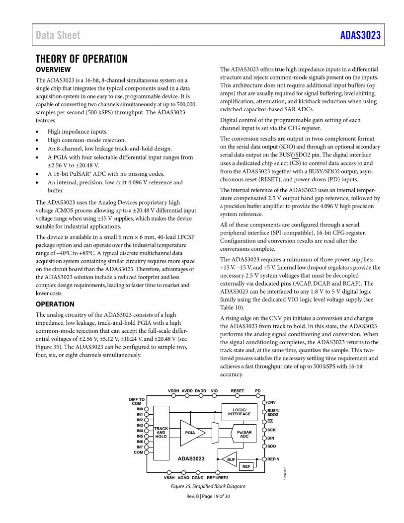
THEORY OF OPERATION OVERVIEW The ADAS3023 is a 16-bit, 8-channel simultaneous system on a single chip that integrates the typical components used in a data acquisition system in one easy to use, programmable device. It is capable of converting two channels simultaneously at up to 500,000 samples per second (500 kSPS) throughput. The ADAS3023 features
• High impedance inputs. • High common-mode rejection. • An 8-channel, low leakage track-and-hold design. • A PGIA with four selectable differential input ranges from
±2.56 V to ±20.48 V. • A 16-bit PulSAR® ADC with no missing codes. • An internal, precision, low drift 4.096 V reference and
buffer.
The ADAS3023 uses the Analog Devices proprietary high voltage iCMOS process allowing up to a ±20.48 V differential input voltage range when using ±15 V supplies, which makes the device suitable for industrial applications.
The device is available in a small 6 mm × 6 mm, 40-lead LFCSP package option and can operate over the industrial temperature range of −40°C to +85°C. A typical discrete multichannel data acquisition system containing similar circuitry requires more space on the circuit board than the ADAS3023. Therefore, advantages of the ADAS3023 solution include a reduced footprint and less complex design requirements, leading to faster time to market and lower costs.
OPERATION The analog circuitry of the ADAS3023 consists of a high impedance, low leakage, track-and-hold PGIA with a high common-mode rejection that can accept the full-scale differ-ential voltages of ±2.56 V, ±5.12 V, ±10.24 V, and ±20.48 V (see Figure 35). The ADAS3023 can be configured to sample two, four, six, or eight channels simultaneously.
The ADAS3023 offers true high impedance inputs in a differential structure and rejects common-mode signals present on the inputs. This architecture does not require additional input buffers (op amps) that are usually required for signal buffering, level shifting, amplification, attenuation, and kickback reduction when using switched capacitor-based SAR ADCs.
Digital control of the programmable gain setting of each channel input is set via the CFG register.
The conversion results are output in twos complement format on the serial data output (SDO) and through an optional secondary serial data output on the BUSY/SDO2 pin. The digital interface uses a dedicated chip select (CS) to control data access to and from the ADAS3023 together with a BUSY/SDO2 output, asyn-chronous reset (RESET), and power-down (PD) inputs.
The internal reference of the ADAS3023 uses an internal temper-ature compensated 2.5 V output band gap reference, followed by a precision buffer amplifier to provide the 4.096 V high precision system reference.
All of these components are configured through a serial peripheral interface (SPI-compatible), 16-bit CFG register. Configuration and conversion results are read after the conversions complete.
The ADAS3023 requires a minimum of three power supplies: +15 V, −15 V, and +5 V. Internal low dropout regulators provide the necessary 2.5 V system voltages that must be decoupled externally via dedicated pins (ACAP, DCAP, and RCAP). The ADAS3023 can be interfaced to any 1.8 V to 5 V digital logic family using the dedicated VIO logic level voltage supply (see Table 10).
A rising edge on the CNV pin initiates a conversion and changes the ADAS3023 from track to hold. In this state, the ADAS3023 performs the analog signal conditioning and conversion. When the signal conditioning completes, the ADAS3023 returns to the track state and, at the same time, quantizes the sample. This two-tiered process satisfies the necessary settling time requirement and achieves a fast throughput rate of up to 500 kSPS with 16-bit accuracy.
BUF
REF
LOGIC/INTERFACE
TRACKAND
HOLDPGIA PulSAR
ADC
DIFF TOCOM
IN0CNV
CS
SCK
DIN
SDO
REFIN
BUSY/SDO2IN1
IN2IN3IN4IN5IN6IN7
COM
VDDH AVDD DVDD VIO RESET
REF1/REF2DGNDAGNDVSSH
PD
ADAS3023
1094
2-00
7
Figure 35. Simplified Block Diagram

ADAS3023 Data Sheet
Rev. B | Page 20 of 30
CNV
PHASE CONVERSION ACQUISITION
tCYC
tCONV tACQ
1094
2-00
8
Figure 36. System Timing
Regardless of the type of signal (single-ended symmetric or asymmetric), the ADAS3023 converts all signals present on the enabled inputs and COM pin in a differential fashion identical to an industry-standard differential or instrumentation amplifier.
The conversion results are available after the conversion completes and can be read back at any time before the end of the next con-version. Avoid reading back data during the quiet period, indicated by BUSY/SDO2 being active high. Because the ADAS3023 has an on-board conversion clock, the serial clock (SCK) is not required for the conversion process; it is only required to present results to the user.
TRANSFER FUNCTIONS The ideal transfer characteristic for the ADAS3023 is shown in Figure 37. The inputs are configured for differential input ranges and the data outputs are in twos complement format, as shown in Table 7.
100...000100...001100...010
011...101011...110011...111
TWOSCOMPLEMENT
STRAIGHTBINARY
000...000000...001000...010
111...101111...110111...111
AD
C C
OD
EANALOG INPUT
+FSR – 1.5LSB+FSR – 1LSB–FSR + 1LSB–FSR
–FSR + 0.5LSB
1094
2-00
9
Figure 37. ADC Ideal Transfer Function
Table 7. Output Codes and Ideal Input Voltages Description Differential Analog Inputs, VREF = 4.096 V Digital Output Code (Twos Complement Hex) FSR − 1 LSB (32,767 × VREF)/(32,768 × PGIA gain) 0x7FFF Midscale + 1 LSB (VREF/(32,768 × PGIA gain)) 0x0001 Midscale 0 0x0000 Midscale − 1 LSB −(VREF/(32,768 × PGIA gain)) 0xFFFF Negative FSR + 1 LSB −(32,767 × VREF)/(32,768 × PGIA gain) 0x8001 Negative FSR −VREF × PGIA gain 0x8000

Data Sheet ADAS3023
Rev. B | Page 21 of 30
IN0IN1IN2IN3IN4IN5IN6IN7
DIFF TOCOM
LOGIC/INTERFACE
REFIN
REF
CNV
RESET
SCK
DIN
SDO
VDDH AVDD DVDD VIO
CS
COM
+
+
+
ENABLE
ADP1613
ADAS3023
COMP
FB FREQ
EN VIN
GND
SS
SW
+ +
VIN = +5V +
+ +
+
VSSH
RF24.22kΩ
RF1B47.5kΩ
RC1100kΩ
CC112nF
CC210pF
CV51µF
REN
RB01Ω
RS10Ω
RS2DNI
CSS1µF Z1
CIN1µF
D1
D2
C11µF
C21µF
L31µF
COUT34.7µF
COUT11µF
COUT22.2µF
+15V
–15V
+5V
ADR434
REF1/REF2
PD
AGND DGND
AD8031
4.096V +
–
1.78ΩRFILT
DNI
50kΩ
L147µH
L247µH
+
+5V+5V
BUF
1094
2-20
0
PGIA PulSARADC
TRACKAND
HOLD
BUSY/SDO2
Figure 38. Complete 5 V, Single-Supply, 8-Channel Data Acquisition System with PGIA
TYPICAL APPLICATION CONNECTION DIAGRAM As shown in Figure 38, the ADP1613 is used in an inexpensive SEPIC-Ćuk topology, which is an ideal candidate for providing the ADAS3023 with the necessary high voltage ±15 V robust supplies (at 20 mA) and low output ripple (3 mV maximum) from an external 5 V supply. The ADP1613 satisfies the specification requirements of the ADAS3023 using minimal external compo-nents yet achieves greater than 86% efficiency. See the CN-0201 circuit note for complete information about this test setup.
ANALOG INPUTS Input Structure
The ADAS3023 uses a differential input structure between each of the channel inputs, IN0 to IN7, and a common reference, COM, all of which sample simultaneously.
Figure 39 shows an equivalent circuit of the inputs. The diodes provide electrostatic discharge (ESD) protection for the analog inputs (IN0 to IN7) and COM from the high voltage supplies (VDDH and VSSH). Ensure that the analog input signal does not exceed the supply rails by more than 0.3 V, which can cause the diodes to become forward-biased and to start conducting current. The voltages beyond the absolute maximum ratings may cause permanent damage to the ADAS3023 (see Table 4).
CPIN
INx OR COM
VSSH
AGND
VDDH
PGIA
1094
2-01
0
TRACKAND
HOLD
Figure 39. Equivalent Analog Input Circuit
Programmable Gain
The ADAS3023 incorporates a PGIA with four selectable ranges. The PGIA settings are specified in terms of the maximum absolute differential input voltage across an input pin and the COM pin, for example, INx to COM. The power-on and default conditions are preset to the ±20.48 V (PGIA = 11) input range.
Note that because the ADAS3023 can use any input type, such as bipolar single-ended and pseudo bipolar, setting the PGIA is important to make full use of the allowable input span.

ADAS3023 Data Sheet
Rev. B | Page 22 of 30
Table 8 describes each differential input range and the corre-sponding LSB size, PGIA bit settings, and PGIA gain.
Table 8. Differential Input Ranges, LSB Size, and PGIA Settings
Differential Input Ranges, INx − COM (V) LSB (μV)
PGIA CFG
PGIA Gain (V/V)
±20.48 625 11 0.2 ±10.24 312.5 00 0.4 ±5.12 156.3 01 0.8 ±2.56 78.13 10 1.6
Common-Mode Operating Range
The differential input common-mode operating range changes according to the input range selected for a given channel and the high voltage power supplies. Note that the operating input voltage of any input pin, as defined in the Specifications section, requires a minimum of 2.5 V of headroom from the VDDH/VSSH supplies or
(VSSH + 2.5 V) ≤ INx/COM ≤ (VDDH – 2.5 V)
The following sections offer some examples of setting the PGIA for various input signals. Note that the ADAS3023 always takes the difference between the INx and COM signals.
Single-Ended Signals with a Nonzero DC Offset (Asymmetrical)
When a 5.12 V p-p signal with a 2.56 V dc offset is connected to one of the inputs (INx+) and the dc ground sense of the signal is connected to COM, the PGIA gain configuration is set to 01 for the ±5.12 V range because the maximum differential voltage across the inputs is +5.12 V. This scenario uses only half the codes available for the transfer function.
ADAS3023
INx+INx+
+5.12V 5.12V p-p
COM
0VCOM
VOFF
VOFF
1094
2-01
1
Figure 40. Typical Single-Ended Unipolar Input Using Only Half of the Codes
Single-Ended Signals with a 0 V DC Offset (Symmetrical) Compared with the example in the Single-Ended Signals with a Nonzero DC Offset (Asymmetrical) section, a better solution for single-ended signals, when possible, is to remove as much differential dc offset between INx and COM as possible such that the average voltage is 0 V (symmetrical around the ground sense). The differential voltage across the inputs is never greater than ±2.56 V, and the PGIA gain configuration is set for a ±2.56 V range (10). This scenario uses all of the codes available for the transfer function, making full use of the allowable differential input range.
ADAS3023
INx+INx+
+2.56V
5.12V p-p
COM
–2.56VCOM
0V
1094
2-01
2
Figure 41. Optimal Single-Ended Configuration Using All Codes
Notice that the voltages in the examples are not integer values due to the 4.096 V reference and the scaling ratios of the PGIA. The maximum allowed dc offset voltage on the COM input pin for various PGIA gains in this case is shown in Table 9.
Table 9. DC Offset Voltage on COM Input and PGIA Settings1 PGIA Gain (V/V) DC Offset Voltage on COM (V) 0.2 0 0.4 0 0.8 ±5.12 1.6 ±7.68 1 Full-scale signal on INx.
VOLTAGE REFERENCE INPUT/OUTPUT The ADAS3023 allows the choice of an internal reference, an external reference using an internal buffer, or an external reference.
The internal reference of the ADAS3023 provides excellent performance and can be used in nearly any application. Setting the reference selection mode uses the internal reference enable bit, REFEN, and the REFIN pin as described in the following sections: Internal Reference section, External Reference and Internal Buffer section, External Reference section, and Reference Decoupling section.
Internal Reference
The precision internal reference is factory trimmed and is suitable for most applications.
Setting the REFEN bit in the CFG register to 1 (default) enables the internal reference and produces 4.096 V on the REF1 and REF2 pins; this 4.096 V output serves as the main system reference. The unbuffered 2.5 V (typical) band gap reference voltage is output on the REFIN pin, which requires an external parallel combination of a 10 μF capacitor and a 0.1 μF capacitor to reduce the noise on the output. Because the current output of REFIN is limited, it can be used as a source when followed by a suitable buffer, such as the AD8031. Note that excessive loading of the REFIN output lowers the 4.096 V system reference because the internal amplifier uses a fixed gain.
The internal reference output is trimmed to the targeted value of 4.096 V with an initial accuracy of ±8 mV. The reference is also temperature compensated to provide a typical drift of ±5 ppm/°C.

Data Sheet ADAS3023
Rev. B | Page 23 of 30
When the internal reference is used, decouple the ADAS3023, as shown in Figure 42. Note that both the REF1 and REF2 con-nections are shorted together and externally decoupled with suitable decoupling on the REFIN output and the RCAP internally regulated supply.
ADAS3023
REFN REF2
10µF
0.1µF
REFN REF1
10µF
0.1µF
REFN REFIN
10µF
0.1µF
BANDGAP
RCAP1µF
RGND
1094
2-0
13
Figure 42. 4.096 V Internal Reference Connection
External Reference and Internal Buffer
The external reference and internal buffer are useful when a common system reference is used or when improved drift performance is required.
Setting Bit REFEN to 0 disables the internal band gap reference, allowing the user to provide an external voltage reference (2.5 V typical) to the REFIN pin. The internal buffer remains enabled, thus reducing the need for an external buffer amplifier to generate the main system reference. Where REFIN = 2.5 V and REF1 and REF2 output 4.096 V, the output voltage serves as the main system reference.
For this configuration, connect the external source, as shown in Figure 43. Any type of 2.5 V reference can be used in this config-uration (low power, low drift, small package, and so forth) because the internal buffer handles the dynamics of the ADAS3023 reference requirements.
ADAS3023
REFN REF2
10µF
0.1µF
REFN REF1
10µF
0.1µF
REFN REFIN
10µF
0.1µF
BANDGAP
RCAP1µF
RGND
REFERENCESOURCE = 2.5V
10
94
2-01
4
Figure 43. External Reference Using Internal Buffer
External Reference
For applications that require a precise, low drift, 4.096 V reference, an external reference can be used. Note that in external reference mode, disabling the internal buffer requires setting REFEN to 0, and driving or connecting REFIN to AGND; thus, both hardware and software control are necessary. Attempting to drive the REF1 and REF2 pins alone prior to disabling the internal buffer can cause source/sink contention in the outputs of the driving amplifiers.
Connect the precision 4.096 V reference directly to REF1 and REF2, which are the main system reference (see Figure 44); two recommended references are the ADR434 or ADR444.
If an op amp is used as an external reference source, take note of the concerns regarding driving capacitive loads. Capacitive loading for op amps usually refers to the ability of the amplifier to remain marginally stable in ac applications but can also play a role in dc applications, such as a reference source.
Keep in mind that the reference source sees the dynamics of the bit decision process on the reference pins, and further analysis beyond the scope of this data sheet may be required.
ADAS3023
REFN REF2
10µF
0.1µF
REFN REF1
10µF
0.1µF
REFIN
BANDGAP
RCAP1µF
RGND
REFERENCESOURCE = 4.096V
10
94
2-0
15
Figure 44. External Reference
Reference Decoupling
With any of the reference topologies described in the Voltage Reference Input/Output section, the REF1 and REF2 reference pins of the ADAS3023 have dynamic impedances and require sufficient decoupling, regardless of whether the pins are used as inputs or outputs. This decoupling usually consists of a low equivalent series resistor (ESR) capacitor connected to each REF1 and REF2 pin and to the accompanying REFN return paths. Ceramic chip capacitors (X5R, 1206 size) are recommended for decoupling in all of the reference topologies described in the Voltage Reference Input/Output section.
The placement of the reference decoupling capacitors plays an important role in system performance. Using thick PCB traces, mount the decoupling capacitors on the same side as the ADAS3023, close to the REF1 and REF2 pins. Route the return paths to the REFN inputs that, in turn, connect to the analog ground plane of the system. When it is necessary to connect to an internal PCB, minimize the resistance of the return path to ground by using as many through vias as possible.
Using the shortest distance and several vias, connect the REFN and RGND inputs to the analog ground plane of the system, preferably adjacent to the solder pads. One common mistake is to route these traces to an individual trace that connects to the ground of the system. This layout can introduce noise, which may adversely affect the LSB sensitivity. To prevent such noise, use PCBs with multiple layers, including ground planes, rather than using single or double sided boards.
Smaller reference decoupling capacitor values (as low as 2.2 μF) can be used with little impact, mainly on DNL and THD. Further-more, there is no need for an additional lower value ceramic

ADAS3023 Data Sheet
Rev. B | Page 24 of 30
decoupling capacitor (for example, 100 nF) that is common in decoupling schemes for high frequency noise rejection.
For applications that use multiple ADAS3023 devices or other PulSAR ADCs, using the internal reference buffer is most effective to buffer the external reference voltage and, thereby, reduce SAR conversion crosstalk.
The reference voltage temperature coefficient (TC) directly affects the full-scale accuracy of the system; therefore, in applications where full-scale accuracy is crucial, care must be taken with the TC. For example, a ±15 ppm/°C TC of the reference changes the full-scale accuracy by ±1 LSB/°C.
POWER SUPPLY The ADAS3023 uses five supplies: AVDD, DVDD, VIO, VDDH, and VSSH (see Table 10). Note that the ACAP, DCAP, and RCAP pins are for informational purposes only because they are the outputs of the internal supply regulators.
Table 10. Supplies Mnemonic Function Required AVDD Analog 5 V core Yes DVDD Digital 5 V core Yes, or can connect to
AVDD VIO Digital input/output Yes, and can connect to
DVDD (for the 5 V level) VDDH Positive high voltage Yes, +15 V typical VSSH Negative high
voltage Yes, −15 V typical
ACAP Analog 2.5 V core No, on chip DCAP Digital 2.5 V core No, on chip RCAP Analog 2.5 V core No, on chip
Core Supplies
The AVDD and DVDD pins supply the ADAS3023 analog and digital cores, respectively. Sufficient decoupling of these supplies is required, consisting of at least a 10 μF capacitor and 0.1 μF capacitor on each supply. Place the 100 nF capacitors as close as possible to the ADAS3023. To reduce the number of supplies that are required, supply the DVDD from the analog supply by connecting a simple RC filter between AVDD and DVDD, as shown in Figure 45.
+
AVDD AGND DVDD DGND
10µF+
10µF 100nF100nF
20Ω +5V DIGITALSUPPLY
+5V ANALOGSUPPLY
VIO+
10µF
+1.8V TO +5VDIGITAL I/O
SUPPLY
100nF
+15V
–15V
+10µF 100nF
+10µF 100nF
VDDH
VSSH
ADAS3023DGND
10
942
-01
6
Figure 45. Supply Connections
VIO is the variable digital input/output supply and allows direct interface with any logic between 1.8 V and 5 V (DVDD supply maximum). To reduce the supplies that are required, VIO can, alternatively, be connected to DVDD when DVDD is supplied from the analog supply through an RC filter. The recommended low dropout regulators are the ADP3334, ADP1715, ADP7102, and ADP7104 for the AVDD, DVDD, and VIO supplies. Note that the user must bring up the ADAS3023 power supplies in the following sequence, shown in Figure 46.
It is recommended to tie the CS, RESET, and PD pins to the VIO supply rail through the use of weak pull-up resistors (10 kΩ or greater) and to design any associated control logic or microcontroller firmware to maintain the state of these signals in the logic high state until all power rails have reached their steady state value. At this time, the PD pin can be deasserted, enabling the internal voltage regulators. The regulators must be allowed to fully power up before RESET is deasserted.
VIO
VSSH
VDDH
AVDD
DVDD
REFIN/REF1/REF2
PD
RESET
109
42-1
41
Figure 46. Power-Up Sequence
Alternative Sequencing
When the constraints of the power supply design prevent the application of the ideal sequence, it is recommended that the designer adhere to the following constraints in the design process:
Apply VSSH as early in the system sequence as possible to ensure that the substrate of the device is appropriately biased.
VSSH must be applied before applying DVDD. VIO must be applied before applying DVDD. DVDD must be applied before or at the same time AVDD
is applied. AVDD must be applied before applying an external
reference.
High Voltage Supplies
The high voltage bipolar supplies, VDDH and VSSH, are required and must be at least 2.5 V larger than the maximum operating input voltage. Specifically, any operating input voltage (as defined in Table 2) of an input pin requires 2.5 V of headroom from the VDDH/VSSH supplies or
(VSSH + 2.5 V) ≤ INx/COM ≤ (VDDH − 2.5 V)

Data Sheet ADAS3023
Rev. B | Page 25 of 30
POWER DISSIPATION MODES The ADAS3023 offers two power dissipation modes: fully operational mode and power-down mode.
Fully Operational Mode
In fully operational mode, the ADAS3023 can perform the conversions normally.
Power-Down Mode
To minimize the operating currents of the device when it is idle, place the device in full power-down mode by bringing the PD input high; power-down mode places the ADAS3023 into a deep sleep mode in which CNV activity is ignored and the digital interface is inactive. Refer to the RESET and Power-Down (PD) Inputs section for timing details. In deep sleep mode, the internal regulators (ACAP, RCAP, and DCAP) and the voltage reference are powered down.
To reestablish operation, return PD to logic low. Note that, before the device can operate at the specified performance, the reference voltage must charge up the external reservoir capacitor(s) and be allowed the specified settling time. RESET must be applied after returning PD to low to restore the ADAS3023 digital core, includ-ing the CFG register, to its default state. Therefore, the desired CFG register value must be rewritten to the device and one dummy conversion must be completed before the device operation is restored to the configuration programmed prior to PD assertion. Note that when using the internal reference, sufficient time is required to settle it to the nominal value. For a typical connection, it requires 100 ms to settle to the nominal value (see Figure 41).
CONVERSION MODES The ADAS3023 offers two conversion modes to accommodate varying applications, and both modes are set with the conversion mode select bit, CMS (Bit 1) of the CFG register.
Warp Mode (CMS = 0)
Setting CMS to 0 is useful where the full 2-channel throughput of 500 kSPS is required. However, in this mode, the maximum time between conversions is restricted. If this maximum period is exceeded, the conversion result can be corrupted. Therefore, warp mode is best suited for continuously sampled applications.
Normal Mode (CMS = 1, Default)
Setting CMS to 1 is useful for all applications where the full 500 kSPS sample rate of the device is not required. In this mode, there is no maximum time restriction between conversions. This mode is the default condition from the assertion of an asynchro-nous reset. The main difference between normal mode and warp mode is that the BUSY/SDO2 time, tCONV, is slightly longer in normal mode than in warp mode.

ADAS3023 Data Sheet
Rev. B | Page 26 of 30
DIGITAL INTERFACE The ADAS3023 digital interface consists of asynchronous inputs and a 4-wire serial interface for conversion result readback and configuration register programming.
This interface uses the three asynchronous signals (CNV, RESET, and PD) and a 4-wire serial interface comprised of CS, SDO, SCK, and DIN. CS can also be tied to CNV for some applications.
Conversion results are presented to the serial data output pin (SDO) after the end of a conversion. The 16-bit configuration word, CFG, is programmed on the serial data input pin, DIN, register during the first 16 SCKs of any data transfer. This CFG register controls the settings, such as selecting the number of channels to be converted, the programmable gain settings for each channel group, and the reference choice (see the Configuration Register section for more information).
CONVERSION CONTROL The CNV input initiates conversions for N enabled channels as defined in the CFG register. The ADAS3023 is fully asynchronous and can perform conversions at any frequency from dc up to 500 kSPS, depending on the settings specified in the configuration register and the system serial clock rate.
CNV Rising—Start of Conversion (SOC)
A rising edge on the CNVrising edfe sets all the settings necessary to initiate a conversion. All conversion clocks are generated internally. After a conversion is initiated, the ADAS3023 ignores other activity on the CNV line (governed by the throughput rate) until the end of the conversion.
While the ADAS3023 is performing a conversion and the BUSY/ SDO2 output is driven high, the ADAS3023 uses a unique 2-phase conversion process, allowing for safe data access and quiet time.
The CNV signal is decoupled from the CS pin, allowing multiple ADAS3023 devices to be controlled by the same processor. For applications where SNR is critical, the CNV source requires very low jitter, which is achieved by using a dedicated oscillator or by clocking CNV with a high frequency, low jitter clock. For appli-cations where jitter is more tolerable or a single device is in use, tie CNV to CS. For more information on sample clock jitter and aperture delay, see the MT-007 Mini Tutorial, Aperture Time, Aperture Jitter, Aperture Delay Time—Removing the Confusion.
Although CNV is a digital signal, take care to ensure fast, clean edges with minimal overshoot, undershoot, and ringing. In addition, avoid digital activity close to the sampling instant because such activity can result in degraded SNR performance.
BUSY/SDO2 Falling Edge—End of Conversion (EOC)
The EOC is indicated by BUSY/SDO2 returning low and can be used as a host interrupt. In addition, the EOC gates data access to and from the ADAS3023. If the conversion result is not read prior to the next EOC event, the data is lost. Furthermore, if the CFG update is not completed prior to the EOC, it is discarded and the current configuration is applied to future conversions.
This pipeline ensures that the ADAS3023 has sufficient time to acquire the next sample to the specified 16-bit accuracy.
Register Pipeline
The CFG register is written on the first 16 SCKs following the EOC event, and it is updated on the next EOC event. To ensure that all CFG updates are applied during a known safe instant to the various circuit elements, the asynchronous data transfer is synchronized to the ADAS3023 timing engine using the EOC event. This synchronization introduces an inherent delay between updating the CFG register setting and the application of the configuration to a conversion. This pipeline, from the end of the current conversion (n), consists of a one-deep delay before the CFG setting takes effect. One deep delay means that two SOC and EOC events must elapse before the setting (that is, the new channel, gain, and so forth) takes effect. Note that the nomenclature (n), (n + 1), and so forth is used in the remainder of the following digital sections: the Serial Data Interface section, General Timing section, and Configuration Register section for simplicity. Note, however, that there is no pipeline after the end of a conversion before data can be read back.
RESET AND POWER-DOWN (PD) INPUTS The asynchronous RESET and PD inputs can be used to reset and power down the ADAS3023, respectively. Timing details are shown in Figure 47.
1094
2-01
7
CS
SDO
CNVn – 1
UNDEFINED
n
SEE NOTE
SEE NOTE
n – 2
x x
x
RESET/PD
DISEN
RH ACQ
CCS
CFG n + 1x DEFAULT
NOTES1. WHEN THE DEVICE IS RELEASED FROM RESET, tACQ MUST BE
MET FOR CONVERSION n IF USING THE DEFAULT CFGSETTING FOR CHANNEL IN0. WHEN THE DEVICE IS RELEASEDFROM POWER-DOWN, tACQ IS NOT REQUIRED, AND THE FIRSTTWO CONVERSIONS, n AND n + 1, ARE UNDEFINED.
BUSY/SDO2
Figure 47. RESET and PD Timing
A rising edge on RESET or PD aborts the conversion process and places SDO into high impedance, regardless of the CS level. Note that RESET has a minimum pulse width (active high) time for setting the ADAS3023 into the reset state. See the Configuration Register section for the default CFG setting when the ADAS3023 returns from the reset state. If this default setting is used after RESET is deasserted (Logic 0), for the conversion result to be valid, a period equal to the acquisition time (tACQ) must elapse before CNV can be asserted; otherwise, if a conversion is initiated, the result is corrupted.

Data Sheet ADAS3023
Rev. B | Page 27 of 30
In addition, the output data from the previous conversion is cleared upon a reset; attempting to access the data result prior to initiating a new conversion produces an invalid result.
Upon the device returning from power-down mode or from a reset when the default CFG is not used, there is no tACQ requirement because the first two conversions from power-up are undefined/ invalid because the one-deep delay pipeline requirement must be satisfied to reconfigure the device to the desired setting.
SERIAL DATA INTERFACE The ADAS3023 uses a simple 4-wire interface and is compatible with field programmable gate arrays (FPGAs), digital signal processors (DSPs), and common serial interfaces such as SPI, QSPI™, and MICROWIRE®.
The interface uses the CS, SCK, SDO, and DIN signals. Timing signals for a serial interface are shown in Figure 48. The most significant bit (MSB) data is valid on SDO (and SDO2) upon CS going low and does not require an SCLK falling edge; therefore, the first SCLK falling edge clocks out MSB first.
SDO is activated when CS is asserted. The conversion result is output on SDO and updated on the SCK falling edges. Simulta-neously, the 16-bit CFG word is updated, if needed, on the serial data input (DIN). The state of BUSY/SDO2 (Bit 0) determines the output format of the MSB data when SDO is activated after the EOC. Note that, in Figure 48, SCK is shown as idling high. SCK can idle high or low, requiring the system developer to design an interface that suits setup and hold times for both SDO and DIN.
DIN(MOSI)
SDO(MISO)
CS
SCK
tDINH
tDINS
tSDOV
tSDOH
tSCKL
tSCK
tSCKH tDIS
tEN
1094
2-01
8
Figure 48. Serial Timing

ADAS3023 Data Sheet
Rev. B | Page 28 of 30
GENERAL TIMING The Figure 49 and Figure 50 conversion timing diagrams show the specific timing parameters, including the complete register to conversion and readback pipeline delay. These figures detail the timing from a power-up or from returning from a full power-down by use of the PD input. When the BUSY/SDO2 output is not enabled after the EOC, the data available on the SDO output (MSB first) can be read after the 16 SCK rising edges in sequential fashion (from Channel 0 (CH0) to Channel 7 (CH7)), as shown in Figure 49.
The converter busy signal is always output on the BUSY/SDO2 pin when CS is logic high. When the BUSY/SDO2 output is ena-bled when CS is brought low after the EOC, the SDO outputs the data of Channel 0 to Channel 3 (CH0, CH1, CH2, and CH3), and the SDO2 outputs the data of Channel 4 to Channel 7 (CH4, CH5, CH6, and CH7) after 16 SCK rising edges, as shown in Figure 50. The conversion result output on BUSY/SDO2 pin synchronizes to the SCK falling edges. The conversion results are in twos comple-ment format. Reading or writing data during the quiet conversion phase (tCONV) may cause incorrect bit decisions.
1 16 1 16 1 16 1 16 1 16 1 16
PHASE
SCK
DIN
SDO
BUSY/SDO2
SOC SOC
EOC
NOTE 2NOTE 1
NOTE 4
NOTE 3
NOTE 2
NOTE 1
EOCPOWER
UPCONV
CYC
CNVH
AD
CONVERSION (n) CONVERSION (n + 1)ACQUISITION (n + 1) ACQUISITION (n + 2)
SOC
DATA (n)
CFG (n + 2) CFG (n + 3)
CH0 CH1 CH7 CH0 CH1 CH7
DATA (n + 1)
1094
2-01
9
CBD
NOTES1. DATA ACCESS CAN ONLY OCCUR AFTER CONVERSION. BOTH CONVERSION RESULT AND THE CFG REGISTER ARE UPDATED AT THE END OF THE CONVERSION (EOC).2. A TOTAL OF 16 SCK FALLING EDGES ARE REQUIRED FOR CONVERSION RESULT. AN ADDITIONAL 16 EDGES AFTER THE LAST CONVERSION RESULT ON BUSY READS BACK THE CFG ASSOCIATED WITH CONVERSION.3. CS CAN BE HELD LOW OR CONNECTED TO CNV. CS IS SHOWN WITH FULL INDEPENDENT CONTROL.4. FOR OPTIMAL PERFORMANCE, DATA ACCESS MUST NOT OCCUR DURING THE SAMPLING INSTANT. A MINIMUM TIME OF AT LEAST THE APERATURE DELAY, tAD, MUST LAPSE PRIOR TO DATA ACCESS.
Figure 49. General Timing Diagram with BUSY/SDO2 Disabled
1 16
PHASE
CNV
SCK
DIN
SDO
CS
SOC SOC
EOC
NOTE 1
NOTE 4
NOTE 3
NOTE 2
NOTE 1
EOCPOWER
UPtCONV
tCYC
tCNVH
tAD
CONVERSION (n) CONVERSION (n + 1)ACQUISITION (n + 1) ACQUISITION (n + 2)
SOC
DATA (n)
CFG (n + 2) CFG (n + 3)
DATA (n + 1)
CH0 CH1 CH2 CH3 CH0 CH1 CH2 CH3
1 16 1 16 1 16 1 16 1 16 1 16 1 16
1094
2-02
0
NOTES1. DATA ACCESS CAN ONLY OCCUR AFTER CONVERSION. BOTH CONVERSION RESULT AND THE CFG REGISTER ARE UPDATED AT THE END OF THE CONVERSION (EOC).2. A TOTAL OF 16 SCK FALLING EDGES ARE REQUIRED FOR CONVERSION RESULT. AN ADDITIONAL 16 EDGES AFTER THE LAST CONVERSION RESULT ON BUSY READS BACK THE CFG ASSOCIATED WITH CONVERSION.3. CS CAN BE HELD LOW OR CONNECTED TO CNV. CS IS SHOWN WITH FULL INDEPENDENT CONTROL.4. FOR OPTIMAL PERFORMANCE, DATA ACCESS MUST NOT OCCUR DURING THE SAMPLING INSTANT. A MINIMUM TIME OF AT LEAST THE APERATURE DELAY, tAD, MUST LAPSE PRIOR TO DATA ACCESS.
BUSY/SDO2
CBDCH4 CH5 CH6 CH7 CH4 CH5 CH6 CH7
Figure 50. General Timing Diagram with BUSY/SDO2 Enabled

Data Sheet ADAS3023
Rev. B | Page 29 of 30
CONFIGURATION REGISTER The configuration register, CFG, is a 16-bit programmable register for selecting all of the user-programmable options of the ADAS3023 (see Table 12).
The register is loaded when data is read back for the first 16 SCK rising edges, and it is updated at the next EOC. Note that there is always a one-deep delay when writing to CFG, and when reading back from CFG, it is the setting associated with the current conversion.
The default CFG setting is applied when the ADAS3023 returns from the reset state (RESET = high) to the operational state (RESET = low). When returning from the full power-down state (PD = high) to an enabled state (PD = low), the default CFG setting is not applied and at least one dummy conversion is
required for the user specified CFG to take effect. To ensure that the digital core is in the default state, apply an external reset after the deassertion of PD. The default value is CFG[15:0] = 0xFFFF. To read back the contents of the configuration register, CFG, an additional 16 SCKs are provided after all of the channel data have been read, and CFG is made available on the SDO output. The default CFG settings configure the ADAS3023 as follows:
• Overwrites contents of the CFG register. • Selects the eight input channels mode. • Configures the PGIA gain to 0.20 (±20.48 V). • Enables the internal reference. • Selects normal conversion mode. • Disables the SDO2 readout mode.
Table 11. Configuration Register, CFG Bit Map; Default Value = 0xFFFF (1111 1111 1111 1111) 15 14 13 12 11 10 9 8 7 6 5 4 3 2 1 0 CFG INx INx RSV PGIA PGIA PGIA PGIA PGIA PGIA PGIA PGIA RSV REFEN CMS BUSY/SDO2
Table 12. Configuration Register Description Bit No. Bit Name Description 15 CFG Configuration update. 0 = keeps current configuration settings. 1 = overwrites contents of register. [14:13] INx Selection of the number of channels to be converted simultaneously.
Bit 14 Bit 13 Channels 0 0 2 0 1 4 1 0 6 1 1 8 12 RSV Always set to 1. [11:4] PGIA Programmable gain selection (see the Programmable Gain section). Bit (Odd) Bit (Even) PGIA Gain 0 0 ±10.24 V 0 1 ±5.12 V 1 0 ±2.56 V 1 1 ±20.48 V (default) [11:10] PGIA Sets the gain of IN0. [9:8] PGIA Sets the gain of IN1. [7:6] PGIA Sets the gain of IN3 to IN2. [5:4] PGIA Sets the gain of IN4 to IN7. 3 RSV Always set to 1. 2 REFEN Internal reference (see the Pin Configuration and Function Descriptions section and Voltage Reference Input/Output section). 0 = disables the internal reference. Disable the internal reference buffer by pulling REFIN to ground. 1 = enables the internal reference (default). 1 CMS Conversion mode selection (see the Conversion Modes section). 0 = uses the warp mode for conversions with a time between conversion restriction. 1 = uses the normal mode for conversions (default). 0 BUSY/SDO2 Secondary data output control using the BUSY/SDO2 pin. 0 = enables the device busy status when the CS pin is held high. On the CS falling edge, the MSB of Channel 4 is
presented on the BUSY/SDO2 input and subsequent data is presented on the SCK falling edges. 1 = enables the device busy status only (default). All data is transmitted via the SDO pin on the SCK falling edge.

ADAS3023 Data Sheet
Rev. B | Page 30 of 30
PACKAGING AND ORDERING INFORMATION OUTLINE DIMENSIONS
07-1
9-20
12-B
0.50BSC
BOTTOM VIEWTOP VIEW
PIN 1INDICATOR
EXPOSEDPAD
PIN 1INDICATOR
SEATINGPLANE
0.05 MAX0.02 NOM
0.20 REF
COPLANARITY0.08
0.300.250.18
6.106.00 SQ5.90
1.000.950.85
FOR PROPER CONNECTION OFTHE EXPOSED PAD, REFER TOTHE PIN CONFIGURATION ANDFUNCTION DESCRIPTIONSSECTION OF THIS DATA SHEET.
0.450.400.35
0.25 MIN
*4.704.60 SQ4.50
*COMPLIANT TO JEDEC STANDARDS MO-220-VJJD-5WITH EXCEPTION TO EXPOSED PAD DIMENSION.
401
11 102021
3031
Figure 51. 40-Lead Lead Frame Chip Scale Package [LFCSP]
6 mm × 6 mm Body and 0.95 mm Package Height (CP-40-15)
Dimensions shown in millimeters
ORDERING GUIDE Model1 Temperature Range Package Description Package Option ADAS3023BCPZ −40°C to +85°C 40-Lead Lead Frame Chip Scale Package [LFCSP] CP-40-15 ADAS3023BCPZ-RL7 −40°C to +85°C 40-Lead Lead Frame Chip Scale Package [LFCSP] CP-40-15 EVAL-ADAS3023EDZ −40°C to +85°C Evaluation Board 1 Z = RoHS Compliant Part.
©2013–2017 Analog Devices, Inc. All rights reserved. Trademarks and registered trademarks are the property of their respective owners.
D10942-0-10/17(B)
www.analog.com/ADAS3023