16-bit microcontroller mb90335 series hardware manual
TRANSCRIPT

FUJITSU SEMICONDUCTORCONTROLLER MANUAL
F2MC-16LX16-BIT MICROCONTROLLER
MB90335 SeriesHARDWARE MANUAL
CM44-10137-3E


FUJITSU LIMITED
F2MC-16LX16-BIT MICROCONTROLLER
MB90335 SeriesHARDWARE MANUAL
“Check Sheet” is seen at the following support page
URL : http://www.fujitsu.com/global/services/microelectronics/product/micom/support/index.html
“Check Sheet” lists the minimal requirement items to be checked to prevent problems beforehand in system development.
Be sure to refer to the “Check Sheet” for the latest cautions on development.


Preface
Purpose of This Document and Intended Reader
We sincerely thank you for your continued use of Fujitsu semiconductor products.
MB90335 series is a 16-bit microcontroller designed for applications such as personal computerperipheral device requiring USB communication. The USB function is not only function operationof 12 M bps but also simple HOST operation (Mini-HOST).MB90335 series has functions which are suitable for controlling personal computer peripheraldevices such as display and audio and mobile devices supporting the USB communication.
This manual describes the functions and operations of the MB90335 Series for engineers whodevelop products using the MB90335 Series. Please read through this manual.
For more information on various instructions, refer to "Instruction Manual".
Note: F2MC is the abbreviation of FUJITSU Flexible Microcontroller.
Trademarks
Embedded Algorithm is a trademark of Advanced Micro Devices, Inc.
Other system and product names used in this manual are trademarks of the related companiesor organizations.
The symbols TM and ® are sometimes omitted in the text.
License
Purchase of Fujitsu I2C components conveys a license under the Philips I2C Patent Rights to
use, these components in an I2C system provided that the system conforms to the I2C StandardSpecification as defined by Philips.
Organization of This Document
This manual contains the following 24 chapters and appendix.
Chapter 1 OVERVIEW
This chapter describes basics to give the understanding of the MB90335 series as a wholesuch as the features, block diagrams, and overviews of the functions.
Chapter 2 CPU
This chapter describes the basic knowledge on architecture, specifications, instructions, andothers to provide better understanding of the CPU core functions of the MB90335 Series.
Chapter 3 INTERRUPTS
This chapter describes the overview of interruptions, interrupt vector and interrupt cause,register configuration/function, and interrupt processing operations.
Chapter 4 RESET
This chapter describes the overview of reset, reset cause and oscillation stabilization waittime, and reset operation.
Chapter 5 CLOCK
This chapter describes the overview of the clock, register configuration/function, clock mode,
i

and oscillation stability wait time.
Chapter 6 LOW-POWER CONSUMPTION MODE
This chapter describes the overview of the low-power consumption mode, registerconfiguration/function, and operation of the low-power consumption mode.
Chapter 7 MODE SETTING
This chapter describes the overview of mode settings, mode pin, mode data, and operationin each mode of mode setting.
Chapter 8 I/O PORT
This chapter describes the overview of the I/O port and the register configuration/functionused in the I/O port.
Chapter 9 TIMEBASE TIMER
This chapter describes the overview of the timebase time, register configuration/function,interrupt, and operation of the timebase timer.
Chapter 10 WATCHDOG TIMER
This chapter describes the overview of the watchdog timer, register configuration/function,and operation of the watchdog timer.
Chapter 11 USB FUNCTION
This chapter describes the overview, block diagram, register, and operation of the USBfunction.
Chapter 12 USB Mini-HOST
This chapter describes the features of the USB Mini-HOST, difference from the USB HOST,block diagrams, registers and operations of USB Mini-HOST, and each token flowchart ofUSB Mini-HOST.
Chapter 13 PWC TIMER
This chapter describes an overview of PWC timer, the configuration and function of register,and the PWC timer operation and precaution.
Chapter 14 16-BIT RELOAD TIMER
This chapter describes an overview of 16-bit reload timer, the configuration and functions ofregister and the 16-bit reload timer operation.
Chapter 15 8/16-BIT PPG TIMER
This chapter describes an overview of 8/16-bit PPG timer, the configuration and functions ofregister, and the 8/16-bit PPG timer operation.
Chapter 16 DTP/EXTERNAL INTERRUPT
This chapter describes an overview of DTP/external interrupt, the configuration and functionsof register, and the DTP/external interrupt operation.
Chapter 17 EXTENDED I/O SERIAL INTERFACE
This chapter describes an overview of the extended I/O serial interface, the configurationand function of registers, and operations of extended I/O serial interface.
Chapter 18 UART
This chapter describes the overview of the UART, the configuration/functions of the register,the operation of the UART, the usage note of the UART, and the example of UART program.
ii

Chapter 19 I2C INTERFACE
This chapter gives an overview of I2C interface, the configuration and functions of registers,
and operations of I2C interface.
Chapter 20 ROM MIRROR FUNCTION SELECTION MODULE
This chapter describes the functions of the ROM mirror function selection module and theconfiguration/function of the register.
Chapter 21 ADDRESS MATCH DETECTION FUNCTION
This chapter explains the address match detection function and its operation.
Chapter 22 512 K-bit FLASH MEMORY
This chapter describes the functions and operation of 3 M-bit flash memory, and the methodfor writing/deleting data to the flash memory.
Chapter 23 DUAL OPERATION FLASH
This chapter describes the functions and operation of Dual Operation Flash.
Chapter 24 EXAMPLE of CONNECTING SERIAL WRITING
This chapter describes the serial on-board writing of the flash ROM (Fujitsu standard).
APPENDIX
Appendix includes detailed information on I/O map, interrupt vector, and instruction list,which are not mentioned in this manual and information that is needed for programming.
iii

Copyright ©2005-2006 FUJITSU LIMITED All rights reserved
• The contents of this document are subject to change without notice. Customers are advised to consult withFUJITSU sales representatives before ordering.
• The information, such as descriptions of function and application circuit examples, in this document are presentedsolely for the purpose of reference to show examples of operations and uses of FUJITSU semiconductor device;FUJITSU does not warrant proper operation of the device with respect to use based on such information. When youdevelop equipment incorporating the device based on such information, you must assume any responsibility arisingout of such use of the information. FUJITSU assumes no liability for any damages whatsoever arising out of theuse of the information.
• Any information in this document, including descriptions of function and schematic diagrams, shall not beconstrued as license of the use or exercise of any intellectual property right, such as patent right or copyright, orany other right of FUJITSU or any third party or does FUJITSU warrant non-infringement of any third-party'sintellectual property right or other right by using such information. FUJITSU assumes no liability for anyinfringement of the intellectual property rights or other rights of third parties which would result from the use ofinformation contained herein.
• The products described in this document are designed, developed and manufactured as contemplated for generaluse, including without limitation, ordinary industrial use, general office use, personal use, and household use, butare not designed, developed and manufactured as contemplated (1) for use accompanying fatal risks or dangersthat, unless extremely high safety is secured, could have a serious effect to the public, and could lead directly todeath, personal injury, severe physical damage or other loss (i.e., nuclear reaction control in nuclear facility,aircraft flight control, air traffic control, mass transport control, medical life support system, missile launch controlin weapon system), or (2) for use requiring extremely high reliability (i.e., submersible repeater and artificialsatellite). Please note that FUJITSU will not be liable against you and/or any third party for any claims or damagesarising in connection with above-mentioned uses of the products.
• Any semiconductor devices have an inherent chance of failure. You must protect against injury, damage or lossfrom such failures by incorporating safety design measures into your facility and equipment such as redundancy,fire protection, and prevention of over-current levels and other abnormal operating conditions.
• If any products described in this document represent goods or technologies subject to certain restrictions on exportunder the Foreign Exchange and Foreign Trade Law of Japan, the prior authorization by Japanese government willbe required for export of those products from Japan.
iv

CONTENTS
CHAPTER 1 OVERVIEW ................................................................................................... 11.1 Feature of MB90335 Series ................................................................................................................ 21.2 Block Diagram .................................................................................................................................... 71.3 Package Dimension ............................................................................................................................ 81.4 Pin Assignment ................................................................................................................................... 91.5 Pin Function ...................................................................................................................................... 101.6 I/O Circuit Types ............................................................................................................................... 131.7 Handling of Device ............................................................................................................................ 16
CHAPTER 2 CPU ............................................................................................................ 192.1 Outline Specification of CPU ............................................................................................................ 202.2 Memory Space .................................................................................................................................. 212.3 Register of CPU ................................................................................................................................ 26
2.3.1 Accumulator (A) ........................................................................................................................... 282.3.2 User Stack Pointer (USP) and System Stack Pointer (SSP) ....................................................... 292.3.3 Processor Status (PS) ................................................................................................................. 302.3.4 Program Counter (PC) ................................................................................................................. 332.3.5 Program Count Bank Register (PCB) .......................................................................................... 342.3.6 Direct Page Register (DPR) ........................................................................................................ 352.3.7 General-purpose Registers (Register Bank) ............................................................................... 36
2.4 Prefix Code ....................................................................................................................................... 37
CHAPTER 3 INTERRUPT ............................................................................................... 413.1 Outline of Interrupt ............................................................................................................................ 423.2 Interrupt Cause and Interrupt Vector ................................................................................................ 453.3 Interrupt Control Register and Peripheral Function .......................................................................... 48
3.3.1 Interrupt Control Registers (ICR00 to ICR15) .............................................................................. 503.3.2 Interrupt Control Register Functions ............................................................................................ 52
3.4 Hardware Interrupt ............................................................................................................................ 553.4.1 Operation of Hardware Interrupt .................................................................................................. 583.4.2 Operation Flow of Hardware Interrupt ......................................................................................... 603.4.3 Procedure for Using a Hardware Interrupt ................................................................................... 613.4.4 Multiple Interrupts ........................................................................................................................ 623.4.5 Hardware Interrupt Processing Time ........................................................................................... 64
3.5 Software Interrupt ............................................................................................................................. 663.6 Interrupts by Extended Intelligent I/O Service (EI2OS) ..................................................................... 68
3.6.1 Extended Intelligent I/O Service (EI2OS) Descriptor (ISD) .......................................................... 703.6.2 Each Register of Extended Intelligent I/O Service (EI2OS) Descriptor (ISD) .............................. 723.6.3 Operation of Extended Intelligent I/O Service (EI2OS) ................................................................ 753.6.4 Procedure for Use of Extended Intelligent I/O Service (EI2OS) .................................................. 763.6.5 Extended Intelligent I/O Service (EI2OS) Processing Time ......................................................... 77
3.7 Exception Processing Interrupt ......................................................................................................... 803.8 Interruption by µDMAC ..................................................................................................................... 81
v

3.8.1 µDMAC Function ......................................................................................................................... 823.8.2 Register of µDMAC ...................................................................................................................... 833.8.3 DMA Descriptor Window Register (DDWR) ................................................................................. 903.8.4 Explanation of Operation of µDMAC ........................................................................................... 96
3.9 Exceptions ........................................................................................................................................ 983.10 Stack Operation of Interrupt Processing ........................................................................................... 993.11 Program Example of Interrupt Processing ...................................................................................... 1013.12 Delayed Interrupt Generation Module ............................................................................................. 105
3.12.1 Operation of Delayed Interrupt Generation Module ................................................................... 106
CHAPTER 4 RESET ...................................................................................................... 1074.1 Outline of Reset .............................................................................................................................. 1084.2 Reset Factors and Oscillation Stabilization Wait Times ................................................................. 1104.3 External Reset Pin .......................................................................................................................... 1124.4 Reset Operation .............................................................................................................................. 1134.5 Reset Factor Bit .............................................................................................................................. 1154.6 State of Each Pin at Reset .............................................................................................................. 117
CHAPTER 5 CLOCK ..................................................................................................... 1195.1 Outline of Clock .............................................................................................................................. 1205.2 Block Diagram of Clock Generation Section ................................................................................... 1225.3 Clock Select Register (CKSCR) ..................................................................................................... 1245.4 Clock Mode ..................................................................................................................................... 1265.5 Oscillation Stabilization Wait Time .................................................................................................. 1285.6 Connection of Oscillator and External Clock .................................................................................. 129
CHAPTER 6 LOW-POWER CONSUMPTION MODE ................................................... 1316.1 Outline of Low-Power Consumption Mode ..................................................................................... 1326.2 Block Diagram of Low-power Consumption Control Circuit ............................................................ 1356.3 Low-power Consumption Mode Control Register (LPMCR) ........................................................... 1376.4 CPU Intermittent Operation Mode .................................................................................................. 1406.5 Standby Mode ................................................................................................................................. 141
6.5.1 Sleep Mode ............................................................................................................................... 1426.5.2 Timebase Timer Mode ............................................................................................................... 1446.5.3 Stop Mode ................................................................................................................................. 145
6.6 State Transition Diagram ................................................................................................................ 1476.7 State of the Pin during Standby Mode, and Reset .......................................................................... 1496.8 Precautions when Using Low-power Consumption Mode .............................................................. 150
CHAPTER 7 MODE SETTING ....................................................................................... 1537.1 Mode Setting ................................................................................................................................... 1547.2 Mode Pins (MD2 to MD0) ............................................................................................................... 1557.3 Mode Data ...................................................................................................................................... 156
CHAPTER 8 I/O PORT .................................................................................................. 1598.1 Functions of I/O Ports ..................................................................................................................... 1608.2 I/O Port Register ............................................................................................................................. 161
vi

8.2.1 Port Data Register (PDR0 to PDR2, PDR4 to PDR6) ............................................................... 1628.2.2 Port Direction Register (DDR0 to DDR2, DDR4 to DDR6) ........................................................ 1638.2.3 Other Registers ......................................................................................................................... 164
CHAPTER 9 TIMEBASE TIMER ................................................................................... 1659.1 Overview of Timebase Timer .......................................................................................................... 1669.2 Configuration of Timebase Timer ................................................................................................... 1689.3 Timebase Timer Control Register (TBTC) ...................................................................................... 1709.4 Interrupt of Timebase Timer ........................................................................................................... 1729.5 Operations of Timebase Timer ....................................................................................................... 1739.6 Precautions when Using Timebase Timer ...................................................................................... 1759.7 Program Example of Timebase Timer ............................................................................................ 177
CHAPTER 10 WATCHDOG TIMER ................................................................................ 17910.1 Overview of Watchdog Timer ......................................................................................................... 18010.2 Watchdog Timer Control Register (WDTC) .................................................................................... 18110.3 Configuration of Watchdog Timer ................................................................................................... 18310.4 Operations of Watchdog Timer ....................................................................................................... 18410.5 Precautions when Using Watchdog Timer ...................................................................................... 18610.6 Program Examples of Watchdog Timer .......................................................................................... 187
CHAPTER 11 USB FUNCTION ....................................................................................... 18911.1 Overview of USB Function .............................................................................................................. 19011.2 Block Diagram of USB Function ..................................................................................................... 19111.3 Register of USB Function ............................................................................................................... 192
11.3.1 UDC Control Register (UDCC) .................................................................................................. 19511.3.2 EP0 Control Register (EP0C) .................................................................................................... 19811.3.3 EP1 to EP5 Control Register (EP1C to EP5C) .......................................................................... 20011.3.4 Time Stamp Register (TMSP) ................................................................................................... 20311.3.5 UDC Status Register (UDCS) .................................................................................................... 20411.3.6 UDC Interruption Enable Register (UDCIE) .............................................................................. 20711.3.7 EP0I Status Register (EP0IS) .................................................................................................... 20911.3.8 EP0O Status Register (EP0OS) ................................................................................................ 21111.3.9 EP1 to EP5 Status Register (EP1S to EP5S) ............................................................................ 21411.3.10 EP0 to EP5 Data Register (EP0DT to EP5DT) ......................................................................... 218
11.4 Operation Explanation of USB Function ......................................................................................... 21911.4.1 Detecting Connection and Disconnection .................................................................................. 22211.4.2 Each Register Operation when Command Responds ............................................................... 22411.4.3 Suspend Function ...................................................................................................................... 22611.4.4 Wake-up Function ..................................................................................................................... 22711.4.5 DMA Transfer Function ............................................................................................................. 22811.4.6 NULL Transfer Function ............................................................................................................ 232
CHAPTER 12 USB Mini-HOST ....................................................................................... 23312.1 Feature of USB Mini-HOST ............................................................................................................ 23412.2 Diversity with USB HOST ............................................................................................................... 23512.3 Block Diagram of USB Mini-HOST ................................................................................................. 236
vii

12.4 Register of USB Mini-HOST ........................................................................................................... 23712.4.1 Host Control Register 0, 1(HCNT0/HCNT1) .............................................................................. 24012.4.2 Host Interruption Register (HIRQ) ............................................................................................. 24412.4.3 Host Error Status Register (HERR) ........................................................................................... 24712.4.4 Host State Status Register (HSTATE) ....................................................................................... 25012.4.5 SOF Interruption FRAME Comparison Register (HFCOMP) ..................................................... 25312.4.6 Retry Timer Setting Register (HRTIMER) ................................................................................. 25412.4.7 Host Address Register (HADR) ................................................................................................. 25512.4.8 EOF Setting Register (HEOF) ................................................................................................... 25612.4.9 FRAME Setting Register (HFRAME) ......................................................................................... 25712.4.10 Host Token Endpoint Register (HTOKEN) ................................................................................ 258
12.5 Operation of USB Mini-HOST ......................................................................................................... 26012.5.1 Connection of Device ................................................................................................................ 26112.5.2 Reset of USB Bus ...................................................................................................................... 26312.5.3 Token Packet ............................................................................................................................. 26412.5.4 Data Packet ............................................................................................................................... 26612.5.5 Handshake Packet .................................................................................................................... 26712.5.6 Retry Function ........................................................................................................................... 26812.5.7 SOF Interrupt ............................................................................................................................. 26912.5.8 Error Status ............................................................................................................................... 27112.5.9 Packet End ................................................................................................................................ 27212.5.10 Suspend Resume ...................................................................................................................... 27312.5.11 Cutting of Device ....................................................................................................................... 276
12.6 Each Token Flow Chart of USB Mini-HOST ................................................................................... 277
CHAPTER 13 PWC TIMER ............................................................................................. 27913.1 Overview of PWC Timer ................................................................................................................. 28013.2 Register of PWC Timer ................................................................................................................... 282
13.2.1 PWC Control Status Register (PWCSR) ................................................................................... 28313.2.2 PWC Data Buffer Register (PWCR) .......................................................................................... 28813.2.3 PWC Ratio of Dividing Frequency Control Register (DIVR) ...................................................... 289
13.3 Movement of PWC Timer ............................................................................................................... 29013.3.1 Operation of PWM Timer Functions .......................................................................................... 29113.3.2 Operation of Pulse Width Measurement Function ..................................................................... 29213.3.3 Count Clock Selection and Operation Mode Selection .............................................................. 29313.3.4 Startup and Stop of Timer/Pulse Width Measurement .............................................................. 29513.3.5 Operation of Timer Mode ........................................................................................................... 29713.3.6 Operation of Pulse Width Measurement Mode .......................................................................... 300
13.4 Precautions when Using PWC Timer ............................................................................................. 305
CHAPTER 14 16-BIT RELOAD TIMER ........................................................................... 30714.1 Overview of 16-bit Reload Timer .................................................................................................... 308
14.1.1 Function of 16-bit Reload Timer ................................................................................................ 30914.1.2 Block Diagram of 16-bit Reload Timer ....................................................................................... 311
14.2 Registers of 16-bit Reload Timer .................................................................................................... 31214.2.1 Timer Control Status Register 0 (TMCSR0) .............................................................................. 31314.2.2 16-bit Timer Register 0 (TMR0)/16-bit Reload Register 0 (TMRLR0) ....................................... 317
viii

14.3 Movement of 16-bit Reload Timer .................................................................................................. 31914.3.1 State Transition of Counter Operation ....................................................................................... 32014.3.2 Operation of Internal Clock Mode (Reload Mode) ..................................................................... 32114.3.3 Operation of Internal Clock Mode (Single Shot Mode) .............................................................. 32414.3.4 Event Count Mode ..................................................................................................................... 327
CHAPTER 15 8/16-BIT PPG TIMER ............................................................................... 32915.1 Overview of 8/16-bit PPG Timer ..................................................................................................... 330
15.1.1 Block Diagram of 8/16-bit PPG Timer ....................................................................................... 33115.2 Registers of 8/16-bit PPG Timer ..................................................................................................... 333
15.2.1 PPG0/PPG2 Operation Mode Control Register (PPGC0/PPGC2) ............................................ 33415.2.2 PPG1/PPG3 Operation Mode Control Register (PPGC1/PPGC3) ............................................ 33615.2.3 PPG0 to PPG3 Output Control Register (PPG01/PPG23) ........................................................ 33915.2.4 PPG Reload Registers (PRLL0 to PRLL3, PRLH0 to PRLH3) .................................................. 341
15.3 Operation of 8/16-bit PPG Timer .................................................................................................... 342
CHAPTER 16 DTP/EXTERNAL INTERRUPT ................................................................. 34716.1 Overview of DTP/External Interrupt ................................................................................................ 34816.2 Register of DTP/External Interrupt .................................................................................................. 34916.3 Operation of DTP/External Interrupt ............................................................................................... 35216.4 Precaution of Using DTP/External Interrupt .................................................................................... 354
CHAPTER 17 EXTENDED I/O SERIAL INTERFACE ..................................................... 35717.1 Outline of Extended I/O Serial Interface ......................................................................................... 35817.2 Register in Extended I/O Serial Interface ....................................................................................... 359
17.2.1 Serial Mode Control Status Register (SMCS) ........................................................................... 36017.2.2 Serial Data Register (SDR) ....................................................................................................... 36417.2.3 Communication Prescaler Control Register (SDCR) ................................................................. 365
17.3 Operation of Extended I/O Serial Interface ..................................................................................... 36717.3.1 Shift Clock Mode ....................................................................................................................... 36817.3.2 Operation State of Serial I/O ..................................................................................................... 36917.3.3 Start/Stop Timing of Shift Operation and Timing of I/O ............................................................. 37117.3.4 Interrupt Function ...................................................................................................................... 373
CHAPTER 18 UART ........................................................................................................ 37518.1 Overview of UART .......................................................................................................................... 37618.2 UART Block Diagram ...................................................................................................................... 37818.3 UART Pins ...................................................................................................................................... 38118.4 Register of UART ............................................................................................................................ 382
18.4.1 Serial Control Register 0, 1 (SCR0, SCR1) ............................................................................... 38318.4.2 Serial Mode Register 0, 1 (SMR0, SMR1) ................................................................................. 38518.4.3 Serial Status Register 0, 1 (SSR0, SSR1) ................................................................................. 38718.4.4 Serial Input Data Register 0, 1(SIDR0, SIDR1) and Serial Output Data Register0, 1(SODR0, SODR1)
.................................................................................................................................................. 39018.4.5 UART Prescaler Control Register 0, 1 (UTCR0, UTCR1) and
UART Prescaler Reload Register 0, 1 (UTRLR0, UTRLR1) ...................................................... 39218.5 UART Interrupt ................................................................................................................................ 394
ix

18.5.1 Receive Interrupt Generation and Flag Set Timing ................................................................... 39618.5.2 Transmit Interrupt Generation and Flag Set Timing .................................................................. 398
18.6 UART Baud Rate ............................................................................................................................ 40018.6.1 Baud Rate of the UART Internal Clock Using the Dedicated Baud Rate Generator ................. 40118.6.2 Baud Rate of the External Clock Using the Dedicated Baud Rate Generator ........................... 40218.6.3 Baud Rate of the External Clock (One-to-one Mode) ................................................................ 403
18.7 Explanation of Operation of UART ................................................................................................. 40418.7.1 Operation in Asynchronous Mode (Operation Mode 0 or Operation Mode1) ............................ 40618.7.2 Operation in Synchronous Mode (Operation Mode 2) ............................................................... 40918.7.3 Bidirectional Communication Function (Normal Mode) ............................................................. 41218.7.4 Master/Slave Mode Communication Function (Multi-processor mode) ..................................... 414
18.8 Notes on Using UART .................................................................................................................... 41718.9 Example of UART Programming .................................................................................................... 418
CHAPTER 19 I2C INTERFACE ....................................................................................... 42119.1 I2C Interface Outline ....................................................................................................................... 42219.2 I2C Interface Register ..................................................................................................................... 424
19.2.1 I2C Bus Status Register 0 (IBSR0) ............................................................................................ 42519.2.2 I2C Bus Control Register 0 (IBCR0) .......................................................................................... 42719.2.3 I2C Bus Clock Control Register 0 (ICCR0) ................................................................................ 43319.2.4 I2C Bus Address Register 0 (IADR0) ......................................................................................... 43519.2.5 I2C Bus Data Register 0 (IDAR0) .............................................................................................. 436
19.3 I2C Interface Operation ................................................................................................................... 43719.3.1 Transfer Flow of I2C Interface ................................................................................................... 43919.3.2 Mode Flow of I2C Interface ........................................................................................................ 44119.3.3 Operation Flow of I2C Interface ................................................................................................. 442
CHAPTER 20 ROM MIRROR FUNCTION SELECTION MODULE ................................ 44520.1 Overview of ROM Mirror Function Select Module .......................................................................... 44620.2 ROM Mirror Function Select Register (ROMM) .............................................................................. 447
CHAPTER 21 ADDRESS MATCH DETECTION FUNCTION ......................................... 44921.1 Overview of Address Match Detection Function ............................................................................. 45021.2 Block Diagram of Address Match Detection Function .................................................................... 45121.3 Configuration of Address Match Detection Function ...................................................................... 452
21.3.1 Address Detection Control Register (PACSR) .......................................................................... 45321.3.2 Detect Address Setting Registers (PADR0, PADR1) ................................................................ 455
21.4 Explanation of Operation of Address Match Detection Function .................................................... 45721.4.1 Example of Using Address Match Detection Function .............................................................. 458
21.5 Program Example of Address Match Detection Function ............................................................... 463
CHAPTER 22 512 KBIT FLASH MEMORY .................................................................... 46522.1 Overview of 512 Kbit Flash Memory ............................................................................................... 46622.2 Registers and Sector/Bank Configuration of Flash Memory ........................................................... 46722.3 Flash Memory Control Status Register (FMCS) ............................................................................. 46922.4 Flash Memory Write Control Register (FWR0/FWR1) .................................................................... 47222.5 How to Start Automatic Algorithm of Flash Memory ....................................................................... 477
x

22.6 Reset Vector Addresses in Flash Memory ..................................................................................... 47922.7 Check the Execution State of Automatic Algorithm ........................................................................ 480
22.7.1 Data Polling Flag (DQ7) ............................................................................................................ 48222.7.2 Toggle Bit Flag (DQ6) ................................................................................................................ 48422.7.3 Timing Limit Over Flag (DQ5) .................................................................................................... 48522.7.4 Sector Erase Timer Flag (DQ3) ................................................................................................. 48622.7.5 Toggle Bit 2 Flag (DQ2) ............................................................................................................. 487
22.8 Details of Programming/Erasing Flash Memory ............................................................................. 48922.8.1 Read/Reset State in Flash Memory ........................................................................................... 49022.8.2 Data Programming to Flash Memory ......................................................................................... 49122.8.3 Data Erase from Flash Memory (Chip Erase) ........................................................................... 49322.8.4 Erasing Any Data in Flash Memory (Sector Erasing) ................................................................ 49422.8.5 Sector Erase Suspension .......................................................................................................... 49622.8.6 Sector Erase Resumption .......................................................................................................... 497
CHAPTER 23 DUAL OPERATION FLASH ..................................................................... 49923.1 Overview of Dual Operation Flash .................................................................................................. 50023.2 Register for Dual Operation Flash .................................................................................................. 50123.3 Operation of Dual Operation Flash ................................................................................................. 503
CHAPTER 24 EXAMPLE of CONNECTING SERIAL WRITING .................................... 50524.1 Basic Configuration ......................................................................................................................... 50624.2 Oscillation Clock Frequency and Serial Clock Input Frequency ..................................................... 50824.3 Flash Microcomputer Programmer System Configuration .............................................................. 50924.4 Example of Connecting Serial Writing ............................................................................................ 510
24.4.1 Example Connection in Single-chip Mode (when Using User Power) ....................................... 51124.4.2 Example of Minimum Connection to Flash Microcomputer Programmer (when Using User Power)
.................................................................................................................................................. 513
APPENDIX ......................................................................................................................... 515APPENDIX A Memory Map ........................................................................................................................ 516APPENDIX B Instructions ........................................................................................................................... 528
B.1 Instruction Types ............................................................................................................................ 529B.2 Addressing ..................................................................................................................................... 530B.3 Direct Addressing ........................................................................................................................... 532B.4 Indirect Addressing ........................................................................................................................ 538B.5 Execution Cycle Count ................................................................................................................... 546B.6 Effective address field .................................................................................................................... 549B.7 How to Read the Instruction List .................................................................................................... 550B.8 F2MC-16LX Instruction List ............................................................................................................ 553B.9 Instruction Map ............................................................................................................................... 567
INDEX................................................................................................................................... 589
xi

xii

Main changes in this edition
Page Changes (For details, refer to main body.)
-Pin name is changed.(VBUS → UTEST)
12Functional description in Table 1.5-1 Pin Function (3/3) is changed.(Terminal for state detection of USB cable (Withstand voltage of 5 V). → It is USB test terminal. Requires a pull-down connection in normal use.)
16 Crystal oscillation circuit is changed.(Please ask the crystal maker to evaluate the oscillational characteristics of the crystal and this device. is added.)
17 Note on PLL clock mode operation is changed.
47USB function 3 of Type and Function of USB Interrupt is changed.(The description of VOFF VON is deleted.)
65Table 3.4-3 Compensation Value of Interrupt Handling Time (Z) is changed.(For the external 8-bit, For the external even address, and For the external odd address is deleted.)
78Table 3.6-4 Compensation Value of Interrupt Handling Time (Z) is changed.(At the external 8 bits, At the external even number address, and At the external odd number address is deleted.)
89
Notes is changed.(• To change the mode to sleep or stop make sure that the ENx bit has been set to "0". → • Before changing the mode to the standby mode (sleep mode, stop mode, watch mode, and timebase timer mode) or the CPU intermittent operation mode (main clock intermittent operation mode, PLL clock intermittent mode, and sub-clock intermittent mode), the DMA enable register must be set to "0".)
134Note is changed.(The transition to the standby mode is a prohibited at USB transfering. is added.)
144Note is changed.(• When using the USB, the transition to the timebase timer mode is disabled. is deleted.)
149
*3 of Table 6.7-1 Pin State in Single-chip Mode is changed.(*3: "Input shutoff" indicates the state in which operation of the input gate nearest to the pin is inhibited. "Output Hi-Z"means that the pin is placed at high impedance with the pin driving transistor placed in the drive disabled state. → *3: In the input shutoff state, the input is masked ant the "L" level is passed to the internal.)Note is changed.(If a USB is in use, transition to the sleep mode is inhibited. The mode transits to the stop mode is also inhib-ited during the USB is transferred. → The mode transits to the standby mode is also inhibited during the USB is transferred.)
190 Features of USB Function is changed.(• Function for detecting a connection and disconnection to the USB bus by monitoring the power line. is deleted.)
xiii

193
Figure 11.3-2 Register of USB Function is changed.(The figure of Address:0000D1H is added.)Address:0000E0H(VOFF → -)Address:0000E0H(VON → -)Address:0000E1H(VOFFIE → -)Address:0000E1H(VONIE → -)
195
Figure 11.3-3 UDC Control Register (UDCC) is changed.(The figure of Address 0000D1H is added.)Note is changed.(To deselect the stop mode, set the order of SUSP and USTP in the UDCS to "0". → To deselect the stop mode, set the order of SUSP and USTP in the UDCC to "0".) UDC Control Register (UDCC) is changed.(The explanation of [bit15 to bit8] Reserved bit is added.)
196Note of [bit5] HCON: Host connection bit is changed.(Please clear the HCON bit before releasing reset of RST. is deleted.)
204
Figure 11.3-7 UDC Status Register (UDCS) is changed.(VOFF → -)(VON → -)The explanation of bit7 and bit6 of UDC Status Register (UDCS) is changed.([bit7, bit6] are changed to Undefined bit )
207
Figure 11.3-8 UDC Interrupt Enable Register (UDCIE) is changed.(VOFFIE → Reserved)(VONIE → Reserved)The explanation of bit15 and bit14 of UDC Interruption Permission Register (UDCIE) is changed.([bit15, bit14] are changed to Reserved bit )
220 Operation of USB Function is changed.( Detecting a connection is changed.)( Example Register Initialization and Operation Startup Procedure is added.)
222 11.4.1 Detecting Connection and Disconnection is added.
350
Notes is changed.(• The value of the DTP/external interrupt factor bit (EIRR:ER) is available only when the corresponding DTP/external internal enable bit (ENIR:EN) is set to "1".When the DTP/external interrupt is not enabled (ENIR:EN = 0), the DTP/external interrupt may be set regardless of whether the DTP/external interrupt fac-tor exists or not.• Clear the corresponding DTP/external internal factor bit (ENIR:ER) just before enabling the DTP/external interrupts (ENIR:EN = 1). is added.)
507Vcc of Table 24.1-1 Function of Used Pins is changed.(When you supply the write voltage (VCC=3.3 V ± 0.3 V) from the user system, you need not connect with flash microcomputer programmer. → Supply the write voltage (VCC=3.3 V ± 0.3 V))
522Address of UDC control register in Table A-1 I/O Map is changed.(0000D0H → 0000D0H to 0000D1H)
523Accesses of the following registers in Table A-1 I/O Map are changed.(UDCC, TMSP, UDCS, EP1S, EP2S, EP3S, EP4S, EP5S)
527USB function 3 of Type and Function of USB Interrupt is changed.(VOFF VON is deleted.)
Page Changes (For details, refer to main body.)
xiv

CHAPTER 1OVERVIEW
This chapter describes basics to give the understanding of the MB90335 series as a whole such as the features, block diagrams, and overviews of the functions.
1.1 Feature of MB90335 Series
1.2 Block Diagram
1.3 Package Dimension
1.4 Pin Assignment
1.5 Pin Function
1.6 I/O Circuit Types
1.7 Handling of Device
1

CHAPTER 1 OVERVIEW
1.1 Feature of MB90335 Series
The MB90335 series are 16-bit microcontrollers designed for applications, such as personal computer peripheral devices, that require USB communications. The USB function enables not only 12-Mbps Function operations but also simplified Host operations (Mini-HOST). It is equipped with functions that are suitable for personal computer peripheral devices such as displays and audio devices, and control of mobile devices that support USB communications.
Feature of MB90335 SeriesIn the MB90335 series, there are the following features.
Built-in PLL clock multiplying circuit
• When the original oscillation is 6 MHz. Operating clock (PLL clock) of 3 to 24 MHz can be selected
from: divided-by-two of the original oscillation or 1-, 2-, or 4-times multiplication of the original
oscillation.
A clock for USB is 48 MHz.
• Minimum instruction execution time of 41.6 ns (at oscillation of 6 MHz, four multiplied PLL clock,
operation at Vcc of 3.3 V)
Maximum memory space: 16 M bytes
Instruction system optimized to control usage
• Data type which can be handled: Bit/byte/word/longword
• Standard addressing mode: 23 types
• High-precision operation enhanced by the employed 32-bit accumulator
• Signed multiplication and division, and enhanced RETI instructions
Instruction system that supports high-level language (C language) multitasking
• Adoption of system stack point
• Instruction set symmetry and barrel shift instructions
Higher execution speed: 4-byte queue
Powerful interrupt function (priority is programmable and can be set to eight levels): 8 external
interrupts
Data transfer function
• µDMAC: maximum 16 channels
• Extended intelligent I/O service function: maximum 16 channels
2

CHAPTER 1 OVERVIEW
Capacity of built-in ROM and ROM type
• Mask ROM: 64 Kbytes
• Flash ROM: 64 Kbytes
Built-in RAM
• Mass production products: 4 Kbytes
• Flash products: 4 Kbytes
• Evaluation chip: 28 Kbytes
Process: CMOS Technology
Low-power consumption (standby) mode
• Sleep mode (mode by which the CPU operation clock is stopped)
• Stop mode (mode by which original oscillation is stopped)
• CPU Intermittent operation mode
Package
• LQFP-64 (FPT-64P-M09: 0.65 mm pin pitch)
Operation guaranteed temperature:-40 °C to +85 °C (0 °C to +70 °C when USB is in use)
General-purpose: maximum 45 ports
General-purpose I/O (CMOS): 21 ports
General-purpose I/O ports (input pull-up resistor settable): 16 ports
General-purpose I/O ports (output open drain/5 V tolerant I/O ports): 8 ports
Timer: Time base timer/watchdog timer: 1 channel
8/16-bit PPG timer: 8 bits x 4 channels or 16 bits x 2 channels
16-bit reload timer: 1 channel
16-bit PWC timer: 1 channel
UART: 2 channels
Extended I/O serial interface: 1 channel
I2C interface: 1 channel
DTP/external interrupt: 8 channels
3

CHAPTER 1 OVERVIEW
USB
• USB function (Conform to USB2.0 Full Speed): 1 channel
• USB Mini-HOST: 1 channel
4

CHAPTER 1 OVERVIEW
Product Lineup
Table 1.1-1 MB90335 Series Product Lineup List (1/2)
Product name MB90V330A * MB90F337 MB90337
Classification Evaluation product Flash memory product Mask ROM product
ROM Size None 64 Kbytes 64 Kbytes
RAM Size 28 Kbytes 4 Kbytes 4 Kbytes
Power supply for emulator Provided - -
CPU function
Number of basic instructions: 351Instruction bit length: 8 bits, 16 bitsMinimum instruction execution time: 41.6 ns/24 MHz Addressing type: 23 typesMaximum size of memory space: 16 Mbytes
Port Input/output port (CMOS): 45
8/16-bit PPG timer
Number of channels: 8 bits × 4 channels, 16 bits × 2 channels with mode switching function
PPG operations of byte or 16 bitsPulse waveform output at arbitrary cycle and duty
16-bit reload timerChannel count: 116-bit reload timer operationWith Event Counter
16-bit PWC timer
Channel count: 1 Timer function (selects one clock for a counter from three internal clocks)Pulse width measurement function (selects one clock for a counter from three internal clocks)
UART
Channel count: 2Clock synchronous/asynchronous selectableDedicated baud rate generator Clock synchronizer LSB and MSB can be switched.
I/O Extended serial interfaceChannel count: 1 Clock synchronous transfer LSB first/MSB first
I2C bus communicationChannel count: 1Serial I/O by which Inter IC BUS is supported
DTP/external interruptInput count: 8Interrupt factor: rising edge/falling edge/"L" level/"H" level selectable
USB
USB Function (Conforming to USB2.0 Full Speed)Supports Full speedEndpoint are specifiable up to six.Transfer type: Control, Interrupt, Bulk, or Isochronous transfer possibleDual port RAM (The FIFO mode is supported).USB Mini-HOST Functions
µDMAC Corresponded
5

CHAPTER 1 OVERVIEW
*: It is setting of Jumper switch (TOOL VCC) when Emulator (MB2147-01) is used. Please refer to the
MB2147-01 or MB2147-20 hardware manual (3.3 Emulator-dedicated Power Supply Switching) about
details.
Note:
Writing to the Flash, be sure to perform VCC=3.13 V to 3.60 V more than.
External bus interfaceIt is (multi/no multi correspondence).
None
The others 9 I/O pins with 5 V tolerant (including pins also used for I2C)
Package PGA299 LQFP64
Operating voltage 3.3 V ± 0.3 V
Table 1.1-1 MB90335 Series Product Lineup List (2/2)
Product name MB90V330A * MB90F337 MB90337
6

CHAPTER 1 OVERVIEW
1.2 Block Diagram
Figure 1.2-1 shows the block diagram of a MB90335 series.
Block Diagram of the MB90335 Series
Figure 1.2-1 Block Diagram of the MB90335 Series
Note:
In Figure 1.2-1, I/O ports share pins with each of built-in functional blocks. Any port used for built-inmodule pin cannot be used as an I/O port.
X0,X1
RST
P67/INT7/SDA0P66/INT6/SCL0P65/INT5/PWCP64/INT4/SCKP63/INT3/SOTP62/INT2/SIN
P61/INT1P60/INT0
Port 0P07 to P00
DVPDVMHVPHVMHCONUTEST
P47/SCK1P46/SOT1P45/SIN1P44/SCK0P43/SOT0P42/SIN0P41/TOT0P40/TIN0
Port 1P17 to P10
P27/PPG3P26/PPG2P25/PPG1P24/PPG0P23P22P21P20
P54P53P52P51P50
Vss Vcc MD0 MD1 MD2
Port 2
8/16bit PPG(ch0,ch1)
8/16-bit PPG(ch.0,ch.1)
CPU F2MC-16LX core
Clockcontrol circuit
RAM(4Kbyte)*
ROM(64Kbyte)*
Interrupt controller
F2 M
C-1
6LX
BU
S
USB function
USB Mini-HOST
Port 4
Port 5
UART(ch.0,ch.1)
16-bit reloadtimer (ch.0)
Port 6
External interrupt
16-bit PWC
I2C interface(ch.0)
Extended I/O serialinterface
(ch.0 to ch.7)
Other pins
*: Maximum value
7

CHAPTER 1 OVERVIEW
1.3 Package Dimension
MB90335 series is available in one type of package.
Package Dimension (LQFP-64)
Figure 1.3-1 Package Dimension of LQFP-64 Type
64-pin plastic LQFP Lead pitch 0.65 mm
Package width ×package length
12 × 12 mm
Lead shape Gullwing
Sealing method Plastic mold
Mounting height 1.70 mm MAX
Code(Reference)
P-LQFP64-12×12-0.65
64-pin plastic LQFP(FPT-64P-M09)
(FPT-64P-M09)
C 2003 FUJITSU LIMITED F64018S-c-3-5
0.65(.026)
0.10(.004)
1 16
17
3249
64
3348
12.00±0.10(.472±.004)SQ
14.00±0.20(.551±.008)SQ
INDEX
0.32±0.05(.013±.002)
M0.13(.005)
0.145±0.055(.0057±.0022)
"A"
.059 –.004+.008
–0.10+0.20
1.50
0~8˚
0.25(.010)
(Mounting height)
0.50±0.20(.020±.008)0.60±0.15
(.024±.006)
0.10±0.10(.004±.004)
Details of "A" part
(Stand off)
0.10(.004)
*
Dimensions in mm (inches).Note: The values in parentheses are reference values.
Note 1) * : These dimensions do not include resin protrusion.Note 2) Pins width and pins thickness include plating thickness.Note 3) Pins width do not include tie bar cutting remainder.
8

CHAPTER 1 OVERVIEW
1.4 Pin Assignment
Figure 1.4-1 shows the pin assignments of a MB90335 series.
Pin Assignment (FPT-64P-M09)
Figure 1.4-1 Pin Assignments of the MB90335 Series (FPT-64P-M09)
MB90335 Series
(FPT-64P-M09)
UTEST
Vss
DVM
DVP
Vcc
Vss
HVM
HVP
Vcc
HCON
P42/SIN0
P43/SOT0
P44/SCK0
P45/SIN1
P46/SOT1
P47/SCK1
1
2
3
4
5
6
7
8
9
10
11
12
13
14
15
16
48
47
46
45
44
43
42
41
40
39
38
37
36
35
34
33
Vss
X1
X0
P24/PPG0
P23
P22
P21
P20
P17
P16
P15
P14
P13
P12
P11
P10
64 63 62 61 60 59 58 57 56 55 54 53 52 51 50 49
P51
P41
/TO
T0
P40
/TIN
0
P67
/INT7
/SD
A0
P66
/INT6
/SC
L0
P65
/INT5
/PW
C
P64
/INT4
/SC
K
P63
/INT3
/SO
T
P62
/INT2
/SIN
P61
/INT1
P60
/INT0
P27
/PP
G3
P26
/PP
G2
P25
/PP
G1
P50
Vcc
17 18 19 20 21 22 23 24 25 26 27 28 29 30 31 32
P52
P53 Vss
MD
2
MD
1
MD
0
RS
T
P54
P00
P01
P02
P03
P04
P05
P06
P07
TOP VIEW
9
CHAPTER 1 OVERVIEW
1.5 Pin Function
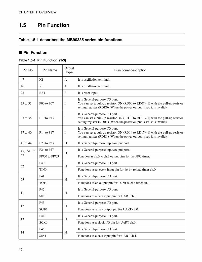
Table 1.5-1 describes the MB90335 series pin functions.
Pin Function
Table 1.5-1 Pin Function (1/3)
Pin No. Pin NameCircuit Type
Functional description
47 X1 A It is oscillation terminal.
46 X0 A It is oscillation terminal.
23 RST F It is reset input.
25 to 32 P00 to P07 I It is General-purpose I/O port.You can set a pull-up resistor ON (RD00 to RD07= 1) with the pull-up resistorsetting register (RDR0) (When the power output is set, it is invalid).
33 to 36 P10 to P13 I It is General-purpose I/O port.You can set a pull-up resistor ON (RD10 to RD13= 1) with the pull-up resistorsetting register (RDR1) (When the power output is set, it is invalid).
37 to 40 P14 to P17 IIt is General-purpose I/O port.You can set a pull-up resistor ON (RD14 to RD17= 1) with the pull-up resistorsetting register (RDR1) (When the power output is set, it is invalid).
41 to 44 P20 to P23 D It is General-purpose input/output port.
45, 51 to53
P24 to P27 D
It is General-purpose input/output port.
PPG0 to PPG3 Function as ch.0 to ch.3 output pins for the PPG timer.
62P40
HIt is General-purpose I/O port.
TIN0 Functions as an event input pin for 16-bit reload timer ch.0.
63P41
HIt is General-purpose I/O port.
TOT0 Functions as an output pin for 16-bit reload timer ch.0.
11 P42
HIt is General-purpose I/O port.
SIN0 Functions as a data input pin for UART ch.0.
12 P43
HIt is General-purpose I/O port.
SOT0 Functions as a data output pin for UART ch.0.
13P44
HIt is General-purpose I/O port.
SCK0 Functions as a clock I/O pin for UART ch.0.
14P45
HIt is General-purpose I/O port.
SIN1 Functions as a data input pin for UART ch.1.
10

CHAPTER 1 OVERVIEW
15P46
HIt is General-purpose I/O port.
SOT1 Functions as a data output pin for UART ch.1.
16P47
HIt is General-purpose I/O port.
SCK1 Functions as a clock I/O pin for UART ch.1.
50 P50 K It is General-purpose I/O port.
64 P51 K It is General-purpose I/O port.
17 P52 K It is General-purpose I/O port.
18 P53 K It is General-purpose I/O port.
24 P54 K It is General-purpose I/O port.
54, 55 P60, P61
C It is General-purpose I/O port (Withstand voltage of 5 V).
INT0, INT1 Function as input pins for external interrupt ch.0 to ch.1.
56
P62
C
It is General-purpose I/O port (Withstand voltage of 5 V).
INT2 Function as input pins for external interrupt ch.2.
SIN It is simple serial I/O data output terminal.
57
P63
C
It is General-purpose I/O port (Withstand voltage of 5 V).
INT3 Function as input pins for external interrupt ch.3.
SOT It is simple serial I/O data output terminal.
58
P64
C
It is General-purpose I/O port (Withstand voltage of 5 V).
INT4 Function as input pins for external interrupt ch.4.
SCK It is simple serial I/O clock input/output terminal.
59
P65
C
It is General-purpose I/O port (Withstand voltage of 5 V).
INT5 Function as input pins for external interrupt ch.5.
PWC Functions as the PWC input pin.
60
P66
C
It is General-purpose I/O port (Withstand voltage of 5 V).
INT6 Function as input pins for external interrupt ch.6.
SCL0 Functions as the clock I/O pin for the I2C interface ch.0.
Set port output to Hi-Z during I2C interface operations.
Table 1.5-1 Pin Function (2/3)
Pin No. Pin NameCircuit Type
Functional description
11

CHAPTER 1 OVERVIEW
61
P67
C
It is General-purpose I/O port (Withstand voltage of 5 V).
INT7 Function as input pins for external interrupt ch.7.
SDA0 Functions as the data I/O pin for the I2C interface ch.0.
Set port output to Hi-Z during I2C interface operations.
1 UTEST C It is USB test terminal.Requires a pull-down connection in normal use.
3 DVM J It is USB Function D- terminal.
4 DVP J It is USB Function D + terminal.
7 HVM J It is USB Mini-HOST D- terminal.
8 HVP J It is USB Mini-HOST D + terminal.
10 HCON J It is external pull-up resistor pin.
21, 22 MD1, MD0 B It is Operation mode select input pin.
20 MD2 G
5 Vcc - It is power supply pin.
9 Vcc - It is power supply pin.
49 Vcc - It is power supply pin.
2 Vss - It is power supply pin (GND).
6 Vss - It is power supply pin (GND).
19 Vss - It is power supply pin (GND).
49 Vss - It is power supply pin (GND).
Table 1.5-1 Pin Function (3/3)
Pin No. Pin NameCircuit Type
Functional description
12

CHAPTER 1 OVERVIEW
1.6 I/O Circuit Types
Table 1.6-1 shows I/O circuit types for pins of a MB90335 series.
I/O Circuit Types
Table 1.6-1 I/O Circuit Types (1/3)
Classification Circuit Remarks
A • Oscillation return resistance: X1, X0 about 1 MΩ
• With standby control
B CMOS hysteresis input
C • CMOS hysteresis input
• N-ch open drain output
D • CMOS output
• CMOS hysteresis input
• With standby control
E CMOS output
X1
X0
N-ch
Standby control signal
Clock inputP-ch
CMOS hysteresis input
CMOS hysteresis input
Standby control signal
N-ch open drain output N-ch
CMOS hysteresis input
P-ch
N-ch
Standby control signal
P-ch
N-ch
Pout
Nout
13

CHAPTER 1 OVERVIEW
F • CMOS hysteresis input with pull-up
• Resistance: About 50 kΩ
G • CMOS hysteresis input with pull-down
• Resistance: About 50 kΩ• Flash product does not have pull-down resistance.
H • CMOS output
• CMOS hysteresis input
• With open drain control
• With standby control
I • CMOS output
• CMOS input
• With input pull-up resistor control
• Resistance: About 50 kΩ• With standby control
Table 1.6-1 I/O Circuit Types (2/3)
Classification Circuit Remarks
CMOS hysteresis input
R
CMOS hysteresis input
R
CMOS hysteresis input
P-ch
N-ch
Open drain control signal
Standby control signal
CMOS input
P-ch
N-ch
Standby control signal
Control signal
14

CHAPTER 1 OVERVIEW
J USB I/O pins
K • CMOS output
• CMOS input (With input interception function at standby)
Table 1.6-1 I/O Circuit Types (3/3)
Classification Circuit Remarks
Full D+ Output
D+ Input
D- Input
Differential inputD+
D-
Full D- Output
Low D- Output
Low D+ Output
direction
speed
CMOS input
Nout
PoutP-ch
N-ch
Standby control signal
15

CHAPTER 1 OVERVIEW
1.7 Handling of Device
This section describes the precautions when handling devices.
Precautions when Handling Devices
Preventing Latch-up, Turning on Power Supply
Latch-up may occur on CMOS IC under the following conditions:
• If a voltage higher than VCC or lower than VSS is applied to input and output pins,
• If a voltage higher than the rated voltage is applied between VCC pin to VSS pin,
• If the AVCC power supply is turned on before the VCC voltage.
Ensure that you apply a voltage to the analog power supply at the same time as VCC or after you turn on the
digital power supply (when you perform power-off, turn off the analog power supply first or at the same
time as VCC and the digital power supply).
When latch-up occurs, power supply current increases rapidly and might thermally damage elements. When
using CMOS IC, take great care to prevent the occurrence of latch-up.
Handling of power supply terminal (VCC/VSS)
To prevent malfunctions of strobe signals due to the rise in the ground level, lower unnecessary
electromagnetic emission level, and prevent latch-up in designing devices if multiple VCC or VSS pins
exist, ensure that you must connect all power supply pins to an external power or a ground line in order to
conform with the total output current rating. And, pay attention to connecting the power sources through as
low impedance as possible to VCC/VSS of a device. In addition, it is recommended to provide a bypass
capacitor of around 0.1µF between VCC/VSS pins near the device.
Crystal oscillation circuit
Noise around X0/X1 pins may cause the malfunctions of a device. Ensure that you should provide bypass
capacitors via shortest distances from X0/X1 and crystal oscillator (or ceramic oscillator) to ground lines,
and try best to prevent lines of crystal oscillation circuits from crossing the lines of other circuits. It is
highly recommended that you should use a printed circuit board artwork because you can expect stable
operations from it.
Please ask the crystal maker to evaluate the oscillational characteristics of the crystal and this device.
16

CHAPTER 1 OVERVIEW
Note on using external clock
If you are using the external clock, you must connect external pins as shown in the Figure 1.7-1.
Figure 1.7-1 illustrates an external clock usage. (under f=7 MHz)
Figure 1.7-1 Method for Using External Clock
Stabilization of supply power supply
A sudden change in the power supply may cause the device to malfunction even within the VCC power
supply voltage operating range. As stabilization guidelines, it is recommended to voltage fluctuations so
control that VCC ripple fluctuations (P-P value) do not exceed 10% of the standard VCC value at the
commercial frequency (50 or 60 MHz) and the transient fluctuation rate does not exceed 0.1 V/ms at power-
on/off etc.
Crystal oscillator circuit of low voltage use
If you are using the device with voltages of 2.0 V or less, the external crystal oscillator may not oscillate at
power-on. Therefore, It will recommend the use of the external clock.
Writing to flash memory
For serial writing to flash memory, always make sure that the operating voltage VCC is between 3.13 V and
3.6 V.
For normal writing to flash memory, always make sure that the operating voltage VCC is between 3.0 V and
3.6 V.
Ensure that you must write to Flash at the operation voltage VCC of 3.0 V to 3.60 V.
Note on PLL clock mode operation
On this microcontroller, if in case the crystal oscillator breaks off or an external reference clock input stops
while the PLL clock mode is selected, a self-oscillator circuit contained in the PLL may continue its
operation at its self-running frequency. However, Fujitsu will not guarantee results of operations if such
failure occurs.
OPEN
X0
X1
17

CHAPTER 1 OVERVIEW
18

CHAPTER 2CPU
This chapter describes specifications, memories and register functions to know the MB90335 series.
2.1 Outline Specification of CPU
2.2 Memory Space
2.3 Register of CPU
2.4 Prefix Code
19

CHAPTER 2 CPU
2.1 Outline Specification of CPU
This chapter explains the outline specification of CPU.
Outline Specification of CPU
The F2MC-16LX CPU core is the 16-bit CPU designed for applications requiring the high-speed real-time
process for house hold device, etc. The F2MC-16LX instruction set is designed for controller applications
enabling the high-speed and high-efficiency control process.
The F2MC-16LX CPU core allows processing not only the 16-bit data but also the 32-bit data by
containing internal 32-bit accumulator (some instructions enabling the 32-bit data process). Maximum 16
Mbytes (extensible) memory space can be accessed by the linear pointer or the bank method. In addition,
the instruction system based on the F2MC-8L family AT architecture is enhanced by the added instruction
compatible to the "H" level language, the extended addressing mode, the enhanced multiplication and
division instructions, and the enriched bit process. Next, the feature of F2MC-16LX CPU is shown.
Minimum instruction execution time
• 41.7 ns/6 MHz original oscillation four-time multiplication (at 24 MHz/3.3 V ± 0.3 V internal operation)
• PLL clock multiplication method
Maximum memory space: 16 Mbytes accessed by the linear/bank method
Instruction system optimized to control usage
• Data type which can be handled: Bit/byte/word/longword
• Standard addressing mode: High-precision operation enhanced by the employed 23 types/32-bit
accumulator
• Signed multiplication and division, and enhanced RETI instructions
Strong interrupt function: Eight propriety levels (programmable)
Automatic forwarding function which is independent from the CPU
• Extended intelligent I/O service function from maximum 16 channels
• µDMAC from maximum 16 channels
Instruction system that supports "H" level language (C language) multitasking
• Adoption of system stack point/Instruction set symmetry/barrel shift instruction
Higher execution speed: 4-byte cue
20

CHAPTER 2 CPU
2.2 Memory Space
The F2MC-16LX CPU has the 16 Mbytes memory space in which all inputs and outputs
of data program that are administered by the F2MC-16LX CPU are placed in this 16 Mbytes memory space. The CPU indicates these addresses with the 24-bit address bus and accesses each resource.
Memory Map
Figure 2.2-1 shows the relation between the F2MC-16LX system and the memory map.
Figure 2.2-1 Example of Relation between F2MC-16LX System and Memory Map
Note:
For memory map of each product, refer to "APPENDIX A Memory Map".
ProgramROM area
RAM area
I/O area
I/O area
Peripheral circuits
Peripheral circuits
Data
EI2OS
Interrupt
Inte
rnal
Bus
General-purposeports
*1 : The size of the internal ROM differs for each model.*2 : The size of the internal RAM differs for each model.
Program area
External area
ROM Mirror area(FF bank image)
Peripheral FunctionControl Register Area
Peripheral FunctionControl Register Area
Interrupt ControlRegister Aria
Peripheral FunctionControl Register Area
I/O Port ControlRegister Aria
Data AreaGeneral-Purpose RegisterEI2OSDescriptor area
Vector table areaFFFFFFHF2MC-16LX deviceFFFC00H
F90000H*1
000020H
000000H
0000C0H
0000FBH
000100H
0000B0H
007900H
001100H*2
000380H000180H
010000H
008000H
Peripheral circuits
F2MC-16LXCPU
21

CHAPTER 2 CPU
Address Generation Type
In F2MC-16LX CPU, there is two address generation method. One is the linear addressing to specify the
entire 24-bit address by the instruction and the other is the bank addressing to specify the upper 8-bit
address and the lower 16-bit address by an appropriate bank register and the instruction, respectively.
There are two types of linear addressing, the method to directly specify the 24-bit address by the operand
and the method to quote the lower 24 bits as the address out of 32-bit general-purpose register content.
Linear addressing (24 bit operand designation)
Figure 2.2-2 shows the example of the linear addressing specified by the 24-bit operand.
Figure 2.2-2 Linear addressing (24-bit Operand Designation)
Linear addressing (indirectly specified by the 32-bit register)
Figure 2.2-3 shows the example of the linear addressing indirectly specified by the 32-bit register.
Figure 2.2-3 Linear addressing (Indirectly Specified by the 32-bit Register)
Old program counter
New program counter
Next instruction
JMPP 123456H
JMPP 123456H
123456H
17452DH
12 3456
17 452D
Old AL
New AL
(Upper 8-bit are ignored)
003A
240906F9
3A090700H
+7
XXXX
MOV A, @RL1+7
RL1
22

CHAPTER 2 CPU
Addressing Types by BankThe bank addressing specifies the bank for each space by five bank registers as shown below by dividing
the 16 Mbytes space into 256 of 64 Kbytes banks:
Program bank register (PCB)
Data bank register (DTB)
User stack bank register (USB)
System stack bank register (SSB)
Additional data bank register (ADB)
The 64 Kbytes bank specified by the PCB is called as the program (PC) space. This PC space contains
instruction codes, vector tables, and immediate value data, for example.
The bank of 64 Kbytes specified by DTB is called data (DT) space. This DT space contains write-enabled
data, internal and external resource control/data registers, etc.
The 64 Kbytes bank specified by USB or SSB is called as the stack (SP) space. This space is accessed
when a stack access occurs at executing the push or pop instruction or saving the interrupt register, etc. The
stack space to be accessed depends on the S flag value in the condition code register.
The 64 Kbytes bank specified by the ADB is called as the additional (AD) space. This AD space contains
the data overflowed from the DT space, etc.
As shown in Table 2.2-1, the default space used in each addressing mode is predefined to improve the
instruction code efficiency. To use a space other than default in an addressing mode, specify the prefix code
corresponding to the bank before specifying the instruction code. This allows you to access an arbitrary
bank space corresponding to the prefix code.
After the reset, the DTB, USB, SSB, and ADB are initialized to 00H and the PCB is initialized to the value
specified by the reset vector. After the reset, each of the DT, SP, and AD spaces is allocated to the bank
00H (000000H to 00FFFFH) and the PC space is allocated to the bank specified by the reset vector.
Figure 2.2-4 shows the example of the memory spaces of the divided register bank.
Table 2.2-1 Default Spaces
Default Spaces Addressing mode
Program space Indirect PC and program access and branch instruction
Data space Addressing mode using @RW0, @RW1, @RW4, and @RW5; @A, addr16, and dir
Stack space Addressing mode using PUSHW, POPW, @RW3, and @RW7
Additional space Addressing mode using @RW2, and @RW6
23
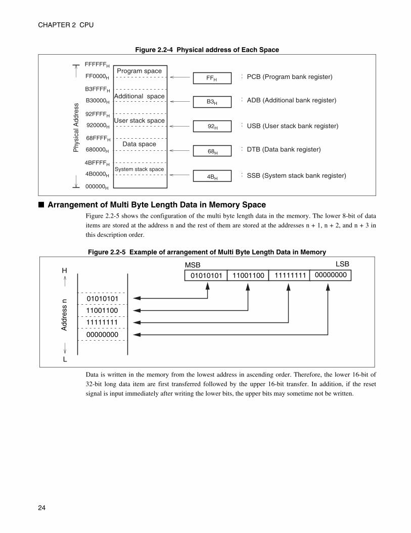
CHAPTER 2 CPU
Figure 2.2-4 Physical address of Each Space
Arrangement of Multi Byte Length Data in Memory SpaceFigure 2.2-5 shows the configuration of the multi byte length data in the memory. The lower 8-bit of data
items are stored at the address n and the rest of them are stored at the addresses n + 1, n + 2, and n + 3 in
this description order.
Figure 2.2-5 Example of arrangement of Multi Byte Length Data in Memory
Data is written in the memory from the lowest address in ascending order. Therefore, the lower 16-bit of
32-bit long data item are first transferred followed by the upper 16-bit transfer. In addition, if the reset
signal is input immediately after writing the lower bits, the upper bits may sometime not be written.
PCB (Program bank register)
ADB (Additional bank register)
USB (User stack bank register)
DTB (Data bank register)
SSB (System stack bank register)
Program space
Additional space
User stack space
Data space
System stack space
Phy
sica
l Add
ress
FFH
B3H
92H
68H
4BH
FFFFFFH
FF0000H
B3FFFFH
B30000H
92FFFFH
920000H
68FFFFH
680000H
4BFFFFH
4B0000H
000000H
Add
ress
n
11001100
01010101
H
L
00000000
11111111
1100110001010101 0000000011111111
LSBMSB
24

CHAPTER 2 CPU
Multi Byte Length Data AccessFundamentally, accesses are made within a bank. For an instruction accessing a multi-byte data item,
address FFFFH is followed by address 0000H of the same bank. Figure 2.2-6 is an example of an instruction
accessing multi-byte data.
This is an example of executing MOVW A, 080FFFFH.
Figure 2.2-6 Example of Multi Byte Length Data access
···
AL before the execution
MOVW A, 080FFFFH
AL after the execution
L
H
800000H
80FFFFH
23H
01H
23H 01H
?? ??
25
CHAPTER 2 CPU
2.3 Register of CPU
The F2MC-16LX registers can be roughly grouped into two types, the special registers in the CPU and the general-purpose registers in memory. Special registers are a dedicated hardware for the CPU inside, and their use is limited by the CPU architecture. General-purpose registers share the CPU address space with the RAM. General-purpose registers are same as special registers so that they can be accessed without specifying the address. However, the user can specify their use same as the normal memory space.
Dedicated Registers
The dedicated registers of F2MC-16LX consist of the following 11 types:
• Accumulator (A = AH: AL): Two 16-bit accumulators (also usable as a single 32-bit accumulator)
• User stack pointer (USP): 16-bit pointer indicating the user stack area
• System stack pointer (SSP): 16-bit pointer indicating the system stack area
• Processor status (PS): 16-bit register indicating the system status
• Program counter: 16-bit register holding the program address
• Program bank register: 8-bit register indicating the PC space
• Data bank register: 8-bit register indicating the DT space
• User stack bank register (USB): 8-bit register indicating the user stack space
• System stack bank register (SSB): 8-bit register indicating the system stack space
• Additional data bank register (ADB): 8-bit register indicating the AD space
• Direct page register (DPR): 8-bit register indicating the direct page
Figure 2.3-1 shows the configuration of the dedicated register.
26

CHAPTER 2 CPU
General-purpose Register
Figure 2.3-1 Configuration of Dedicated Registers
The F2MC-16LX general-purpose registers are present at addresses 000180H to 00037FH (maximum
configuration) of main memory. The register bank pointer (RP) indicates the part in use as current register
bank out of the above mentioned address. In each bank, three kinds of registers shown next exist. They are
dependent each other as shown in Figure 2.3-2.
• R0 to R7: General-purpose register of 8-bit
• RW0 to RW7: General-purpose register of 16-bit
• RL0 to RL3: General-purpose register of 32-bit
Figure 2.3-2 shows the configuration of the general-purpose register.
Figure 2.3-2 Configuration of General-purpose Register
The relationship between the upper and lower bytes of byte register and word register can be expressed by
the equation, RW(i + 4) = RW(i x 2 + 1) x 256 + R(i x 2) [i = 0 to 3] while the relation between the upper
and lower bytes of Rli can be expressed by the equation, RW(i) = RW(i x 2 + 1) x 65536 + RW(i x 2) [i = 0
to 3].
Accumulator
User stack pointer
System stack pointer
Processor status
Program counter
Direct page register
Program bank register
Data bank register
User stack bank register
System stack bank register
Additional data bank register
32-bit16-bit
8-bit
AH AL
USP
PC
SSP
DPR
PS
PCB
DTB
USB
SSB
ADB
16 bit
Upper
Lower RW0
LSB
RW1
RW2
RW3
RL3
RL2
RL1
RL0
RW7
RW6
RW5
RW4
R4
R2
R0
R6R7
R5
R3
R1
MSB
000180H+RPx10H
27

CHAPTER 2 CPU
2.3.1 Accumulator (A)
Here, the function of accumulator (A) is explained.
Accumulator (A)The accumulator (A) consists of two 16-bit length arithmetic operation registers (AH/AL) to be used for the
temporary storage of operation result and data transfer, etc. The AH and the AL are concatenated to be used
for the 32 bit data process. Only the AL is used for the word process in the 16-bit data process mode or for
the byte process in the 8-bit data process mode. Data stored in the accumulator (A) can be used for
operations with data in the memory and registers (Ri, RWi, and Rli). In the same manner as the F2MC-8L,
when a data item shorter than the word length is transferred to the AL, the data item in the AL before the
transfer is automatically transferred to the AH (data hold function). Improvement of the process efficiency
is supported by the data hold function and the operation between AL and AH.
When data shorter than the byte length is transferred to the AL, the data is sign-extended or zero-extended
to 16-bit length data items and stored in the AL. Data in the AL can be handled as those in word or byte
length.
When the arithmetic operation instruction of byte process is executed in the AL, the upper eight-bit of the
AL before operation are ignored and all the upper eight bits of the operation result become 0. The
accumulator (A) value is not initialized by the reset and is undefined value immediately after the reset.
Figure 2.3-3 shows the 32-bit data transfer process, and Figure 2.3-4 shows the AL-AH transfer process.
Figure 2.3-3 32-bit Data Transfer
Figure 2.3-4 AL-AH Transfer
A before the execution
A after the execution
LSB
DTB
38H
MSB
15H
52H
74H
A6H2BH
8FH
8F74H
A6153EH
XXXXH
2B52H RW1
A61540HXXXXH
+6
MOVW A,@RW1+6
A before the execution
A after the execution
LSB
DTB
38H
MSB
15H
52H
74H
A6H2BH
8FH
1234H
A6153EH
1234H
2B52H RW1
A61540HXXXXH
+6
MOVW A,@RW1+6
28
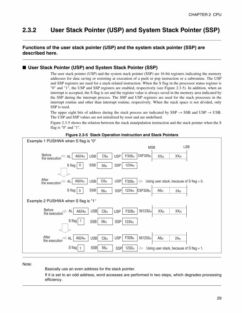
CHAPTER 2 CPU
2.3.2 User Stack Pointer (USP) and System Stack Pointer (SSP)
Functions of the user stack pointer (USP) and the system stack pointer (SSP) are described here.
User Stack Pointer (USP) and System Stack Pointer (SSP)The user stack pointer (USP) and the system stack pointer (SSP) are 16-bit registers indicating the memoryaddresses for data saving or restoring at execution of a push or pop instruction or a subroutine. The USPand SSP registers are used for a stack-related instruction. When the S flag in the processor status register is"0" and "1", the USP and SSP registers are enabled, respectively (see Figure 2.3-5). In addition, when aninterrupt is accepted, the S flag is set and the register value is always saved in the memory area indicated bythe SSP during the interrupt process. The SSP and USP registers are used for the stack processes in theinterrupt routine and other than interrupt routine, respectively. When the stack space is not divided, onlySSP is used.
The upper eight bits of address during the stack process are indicated by SSP → SSB and USP → USB.The USP and SSP values are not initialized by reset and are undefined.
Figure 2.3-5 shows the relation between the stack manipulation instruction and the stack pointer when the Sflag is "0" and "1".
Figure 2.3-5 Stack Operation Instruction and Stack Pointers
Note: Basically use an even address for the stack pointer.
If it is set to an odd address, word accesses are performed in two steps, which degrades processingefficiency.
Example 1 PUSHWA when S flag is "0"
Example 2 PUSHWA when S flag is "1"
Before the execution
After the execution
S flag
S flag
Using user stack, because of S flag = 0.
F328H
56H
C6HA624H
0
AL
SSB
USB
SSP
USP
SSB
USB
SSP
USPA624HAL
0
1234H
C6F326H
F328H
56H
C6H
1234H C6F326H A6H 24H
MSB LSB
XXH XXH
S flag
S flag
Before the execution
After the execution
Using user stack, because of S flag = 1.
F328H
56H
C6HA624H
1
AL
SSB
USB
SSP
USP
SSB
USB
SSP
USPA624HAL
1234H
561232H
F328H
56H
C6H
1232H
A6H 24H
XXH XXH
561232H
1
29

CHAPTER 2 CPU
2.3.3 Processor Status (PS)
Here, the function of processor status (PS) is explained.
Processor Status (PS)The processor status (PS) consists of bits to perform the CPU operation and to indicate the CPU status. As
shown in Figure 2.2-6, the upper byte of PS register consists of the register bank pointer (RP) and the
interrupt level mask register (ILM). The RP indicates the start address of register bank while the lower byte
of PS register is the condition code register (CCR) containing the flag which is set or reset by the execution
result or an interrupt occurrence.
Figure 2.3-6 shows the configuration of the processor status (PS).
Figure 2.3-6 Configuration of Processor Status (PS)
Condition Code Register (CCR)Figure 2.3-7 shows the configuration of the condition code register.
Figure 2.3-7 Configuration of the Condition Code Register (CCR)
Interrupt enable flag (I)
Interrupts other than software interrupt are enabled and masked when the I flag is "1" and "0", respectively.
The I flag is cleared by the reset.
Stack flag (S)
When the S flag is "0" and "1", the USP and the SSP are valid as a stack manipulation pointer, respectively.
The S flag is set by an interrupt or a reset.
Sticky-bit flag (T)
"1" is set to the T flag when the data contain one or more "1" that has been shifted out from a carry after the
execution of logical right or arithmetic right shift instruction. "0" is set otherwise. When the amount of the
shift is "0", "0" is set in T flag.
Negative flag (N)
The N flag is set and cleared when the MSB of operation result is "1" and any other, respectively.
15 0781213
PS ILM RP CCR
Initial value : Undefined value
TS
7 6 5 4 3 2 1 0
I VZN C
10 X X X X X X
30

CHAPTER 2 CPU
Zero flag (Z)
If the operation result is all "0", Z flag is set, and, besides, cleared.
Overflow flag (V)
The V flag is set and cleared when a signed numeric value overflow occurs and does not occur,
respectively, as a result of operation execution.
Carry flag (C)
The C flag is set and cleared when the MSB is carried up or down and is not occurred, respectively, as a
result of operation execution.
Register Bank Pointer (RP)
The register bank pointer (RP) indicates the relation between the F2MC-16LX general-purpose register and
the internal RAM address. The RP indicates the current start memory address of register bank in use by the
conversion expression, (00180H + RP x 10H).
The RP consisting of 5-bit can take values from 00H to 1FH.
The register bank can be allocated to the memory of 000180H to 00037FH. However, it cannot be used as a
general-purpose register even within this range if the register bank is not the internal RAM. The 8-bit
immediate value can be transferred to the RP on the instruction although only the lower 5 bits of those data
are actually used.
Figure 2.3-8 Configuration of Register Bank Pointer (RP)
Interrupt Level Mask Register (ILM) The interrupt level mask register (ILM) consisting of 3-bit indicates the interrupt mask level of CPU. An
interrupt request is accepted only when its level is higher than the level indicated by these 3 bits. Level "0"
is the highest priority interrupt and level "7" is the lowest priority interrupt (see Table 2.3-1). Therefore, an
acceptable interrupt level value must be smaller than the current ILM value. When an interrupt is accepted,
the interrupt level value is set in the ILM and thereafter no interrupt is accepted when its priority is same or
lower than it. ILM is initialized to "0" by reset. The 8-bit immediate value can be transferred to the ILM
register on the instruction although only the lower 3-bit of those data are actually used.
Figure 2.3-9 shows the configuration of the interrupt level mask register while Table 2.3-1 shows the level
indicated by the interrupt level mask register (ILM).
Figure 2.3-9 Configuration of Interrupt Level Mask Register (ILM)
Initial value 0
B4 B0B1B2B3
0000
Initial value
ILM0
000
ILM2 ILM1
31

CHAPTER 2 CPU
Table 2.3-1 Level Indicated by Interrupt Level Mask Register (ILM)
ILM2 ILM1 ILM0 Level value Acceptable interrupt level
0 0 0 0 Disables the interrupt.
0 0 1 1 Only 0
0 1 0 2 Small level value smaller than 1
0 1 1 3 Small level value smaller than 2
1 0 0 4 Small level value smaller than 3
1 0 1 5 Small level value smaller than 4
1 1 0 6 Small level value smaller than 5
1 1 1 7 Small level value smaller than 6
32

CHAPTER 2 CPU
2.3.4 Program Counter (PC)
Here, the function of program counter (PC) is explained.
Program Counter (PC)The PC is a 16-bit counter to indicate the lower 16 bits of memory address of the instruction code to be
executed by the CPU. The upper 8-bit address is indicated by the program count bank register (PCB). The
PC content is updated by the conditional branch instruction, the subroutine call instruction, the interrupt,
the reset, etc. In addition, it can be used as the base pointer at the operand access.
Figure 2.3-10 shows the function of the program counter (PC).
Figure 2.3-10 Function of Program Counter (PC)
Note:
Neither PC nor PCB can be directly rewritten by program (e.g. by a MOV PC, #FF instruction).
Next execution instructionPCB FEH PC
FEABCDH
ABCDH
33

CHAPTER 2 CPU
2.3.5 Program Count Bank Register (PCB)
Here, the function of program count bank register (PCB) is explained.
Program Count Bank Register (PCB) <Initial Value: Value in Reset Vector > Program count bank register (PCB) consists of the following registers:
• Data bank register (DTB) <Initial value:00H>
• User stack bank register (USB) <Initial value:00H>
• System stack bank register (SSB) <Initial value:00H>
• Additional data bank register (ADB) <Initial value:00H>
Each of bank registers indicates the memory bank where the PC, DT, SP (user), SP (system), and AD
spaces are allocated.
Every bank register is 1 byte length. The PCB is initialized to 00H by the reset. The bank registers other
than PCB can be read. PCB cannot be written though can read.
The PCB is updated by the execution of the JMPP, CALLP, RETP, RETI, and RETF instructions that are
branched to 16 Mbytes all spaces or an interrupt occurrence. For the operation of each register, see "2.2
Memory Space".
34

CHAPTER 2 CPU
2.3.6 Direct Page Register (DPR)
Here, the function of direct page register (DPR) is explained.
Direct Page Register (DPR) <Initial Value:01H>
The direct page register (DPR) specifies the addresses 8 to addresses 15 of instruction operand in the direct
addressing mode as shown in Figure 2.3-11. The DPR having the 8-bit length is initialized to 01H by the
reset. In addition, it can be read and written by the instruction.
Figure 2.3-11 shows the generation of the physical address in the direct addressing mode.
Figure 2.3-11 Physical address Generation in the Direct addressing Mode
DTB register DPR registerDirect addressing
during instruct
24-bit physical address
MSB LSB
ααααααααββββββββγγγγγγγγ
ββββββββ γγγγγγγγαααααααα
35

CHAPTER 2 CPU
2.3.7 General-purpose Registers (Register Bank)
Functions of general-purpose registers (register bank) are described here.
General-purpose Registers (Register Bank) The register bank consisting of 8 words can be used as the general-purpose register for arithmetic
operations of the byte register (R0 to R7), the word register (RW0 to RW7), and the long word register
(RL0 to RL3). In addition, the register bank can be used as the instruction pointer. Table 2.3-2 shows the
functions of each register and Figure 2.3-12 shows the relations with each register.
The register bank value is not initialized by the reset as same as the normal RAM area and the status before
the reset is maintained.
However, power becomes irregular when it is on.
Figure 2.3-12 Relations with Each Register
Table 2.3-2 Functions of Each Register
R0 to R7 Used as operands for various instructionsNote: The R0 is also used as the barrel shift counter or the normalization instruction counter.
RW0 to RW7 Used as pointers and operands for various instructionsNote: RW0 can also be used as the string instruction counter.
RL0 to RL3 Used as long pointers and operands for various instructions
R0
R1
R5
R6
R4
R3R2
R7
RW1RL0
RW7
RW6
RW3RW2
RW0
RL2
RL1RL3
RW4
RW5
36

CHAPTER 2 CPU
2.4 Prefix Code
A part of instruction operation can be changed by placing the prefix code before the instruction. Three types of prefix codes can be used: • The bank select prefix• The common register bank prefix• The flag change suppression prefix.
Bank Select PrefixMemory spaces used to access data are defined for each addressing mode.
Placing the bank select prefix before the instruction allows the instruction to select the memory space used
for the data access regardless of addressing mode.
Table 2.4-1 shows the relation between the bank select prefix and the space to be selected.
Be careful when using the following instructions:
String instruction (MOVS,MOVSW,SCEQ,SCWEQ,FILS,FILSW)
The bank register specified by the operand is used regardless of the prefix.
Stack operation instruction (PUSHW,POPW)
The SSB or the USB is used according to the S flag regardless of the prefix.
I/O Access instruction
MOVA A,io/MOV io,A/MOVX A,io/MOVW A,io/MOVW io,A
MOV io,#imm8/MOVW io,#imm8/MOBV A,io:bp/MOVB io:bp,A
SETB io:bp/CLRB io:bp/BBC io:bp,rel/BBS io:bp,rel WBTC
WBTS
The bank I/O space is used regardless of the prefix presence or absence.
Flag change instruction (AND CCR,#imm8,OR CCR,#imm8)
The instruction operation is normal although the prefix continuously affects the next instruction.
Table 2.4-1 Bank Select Prefix
Bank Select Prefix Selected Space
PCC PC space
DTB Data space
ADB AD space
SPB The SSP or USP space is used according to the stack flag value.
37

CHAPTER 2 CPU
POPW PS
The SSB or the USB is used according to the S flag regardless of the prefix. The effect of the prefix reaches
the following instruction.
MOV ILM,#imm8
The instruction operation is normal although the prefix continuously affects the next instruction.
RETI
SSB is used regardless of the prefix.
Common Register Bank Prefix (CMR)To facilitate data exchange between multiple tasks, the same register bank access must be relatively easy
regardless of the register bank pointer (RP) value. When the CMR precedes the instruction to access the
register bank, the instruction accesses the common bank (register bank selected when RP = 0) at the
address of 000180H to 00018FH regardless of the current RP value.
Be careful, however, when using following instructions:
String instruction (MOVS,MOVSW,SCEQ,SCWEQ,FILS,FILSW)
When an interrupt request occurs during the execution of string instruction added with prefix code and the
string instruction returns after the interrupt process, the prefix code is disabled. Therefore, the string
instruction malfunctions after the interrupt process. Please do not add the CMR prefix to the above string
instruction.
Flag change instruction (AND CCR,#imm8,OR CCR,#imm8)
The instruction operation is normal although the prefix continuously affects the next instruction.
MOV ILM,#imm8
The instruction operation is normal although the prefix continuously affects the next instruction.
Flag Change Suppression Prefix (NCC)To suppress the flag change, the flag change suppression prefix code (NCC) is used. Placing the NCC
before the instruction can suppress the flag change accompanying the instruction. Be careful, however,
when using following instructions:
String instruction (MOVS,MOVSW,SCEQ,SCWEQ,FILS,FILSW)
When an interrupt request occurs during the execution of string instruction added with prefix code and the
string instruction returns after the interrupt process, the prefix code is disabled. Therefore, the string
instruction malfunctions after the interrupt process. Please do not add the CMR prefix to the above string
instruction.
Flag change instruction (AND CCR,#imm8,OR CCR,#imm8)
The instruction operation is normal although the prefix continuously affects the next instruction.
38

CHAPTER 2 CPU
Interrupt instruction (INT #vct8,INT9,INT addr16,INTO addr24,POPW PS)
The CCR is changed as specified by the instruction regardless of the prefix.
JCTX@A
The CCR is changed as specified by the instruction regardless of the prefix.
MOV ILM,#imm8
The instruction operation is normal although the prefix continuously affects the next instruction.
Interrupt Suppression InstructionThe interrupt request is not sampled for the following 10 types of instructions:
MOV ILM,#imm8/PCB/SPB/OR CCR,#imm8/NCC
AND CCR,#imm8/ADB/CMR/POPW PS/DTB
When a valid interrupt request occurs during the execution of one of the above instructions, the interrupt
can be processed only if an instruction other than the above is executed. For the details, see Figure 2.4-1.
Figure 2.4-1 Interrupt Suppression Instruction
Constraints on Interrupt Suppression Instructions and Prefix InstructionsWhen a prefix code precedes the interrupt suppression instruction, the prefix code affects up to the first
instruction after codes other than interrupt suppression instructions as shown in Figure 2.4-2.
Figure 2.4-2 Interrupt Suppression Instruction and Prefix Code
Interrupt request Interrupt acceptance
(a) Normal request
Interrupt suppression instruction
(a)
Interrupt suppression instruction
CCR is not changed by NCC.
MOV A, FFH NCC MOV LIM, #imm8 ADD A, 01H
CCR : XXX10XXB
39

CHAPTER 2 CPU
Array of Prefix CodeIf conflicting prefix codes continue, the last one is valid as shown in Figure 2.4-3.
The conflicting prefix code means the PCB, ADB, DTB, and SPB as shown in Figure 2.4-3.
Figure 2.4-3 Array of Prefix Codes
Prefix code
PCB is enabled as prefix code.
DTBADB PCB ADD A, 01H
40

CHAPTER 3INTERRUPT
This chapter describes the interruption, extended intelligent I/O service (EI2OS), and direct memory access controller (µDMAC) of MB90335 Series.
3.1 Outline of Interrupt
3.2 Interrupt Cause and Interrupt Vector
3.3 Interrupt Control Register and Peripheral Function
3.4 Hardware Interrupt
3.5 Software Interrupt
3.6 Interrupts by Extended Intelligent I/O Service (EI2OS)
3.7 Exception Processing Interrupt
3.8 Interruption by µDMAC
3.9 Exceptions
3.10 Stack Operation of Interrupt Processing
3.11 Program Example of Interrupt Processing
3.12 Delayed Interrupt Generation Module
41

CHAPTER 3 INTERRUPT
3.1 Outline of Interrupt
F2MC-16LX has the following five interrupt functions, which suspend the current process when an event occurs and transfer control to a separately defined program.• Hardware Interrupt• Software interrupt
• Interrupts by extended intelligent I/O service (EI2OS)• Interruption by µDMAC• Exception processing
Type and Function of Interrupt
Hardware Interrupt
Transfers control to the user-defined interrupt handling program in response to an interrupt request from a
peripheral function.
Figure 3.1-1 Overview of Hardware Interrupts
IR Check Comparator
InterruptcontrollerLe
vel c
ompa
rato
r
Inte
rrup
t lev
el IL
PS I ILMPSIILMIR
: Processor status: Interrupt enable flag: Interrupt level mask register: Instruction register
AND
F2MC-16LX CPU
Microcode
Register file
Peripheral
Enable FF
Cause FF
F2 M
C-1
6 bu
s
42

CHAPTER 3 INTERRUPT
Software interrupt
Transfers control to the user-defined interrupt handing program by executing the instruction dedicated to
software interrupt (for example, INT instruction).
Figure 3.1-2 Overview of Software Interrupts
Interrupts by extended intelligent I/O service (EI2OS)
EI2OS is involved in automatic data transfer between peripheral functions and memory. EI2OS is capable
of performing data transfer like DMA (direct memory access) although it was previously performed by the
interrupt handling program. Once the data transfer process has been performed the specified number of
times, EI2OS automatically executes the interrupt handling program.
Interruption by EI2OS is a type of hardware interrupt.
Figure 3.1-3 Overview of the Extended Intelligent I/O Service (EI2OS)
RAM
Save
Register file
MicrocodeQueue Fetch
Instruction bus
IR
PS I ILM
F2MC-16LX CPU
F2 M
C-1
6 bu
s
PSIILMIRB unit
: Processor status: Interrupt enable flag: Interrupt level mask register: Instruction register: Bus interface unit
B unit
CPU
by IOA
by BAP
ISD
I/O register I/O registerPeripheral
Interrupt request
Interrupt control register
Interrupt controller
Memory space
Buffer
by ICS
by DCT
I/O requests transferThe interrupt controller selects the descriptor.The transfer source and destinationare read from the descriptor.Data is transferred between I/O and memory.
43
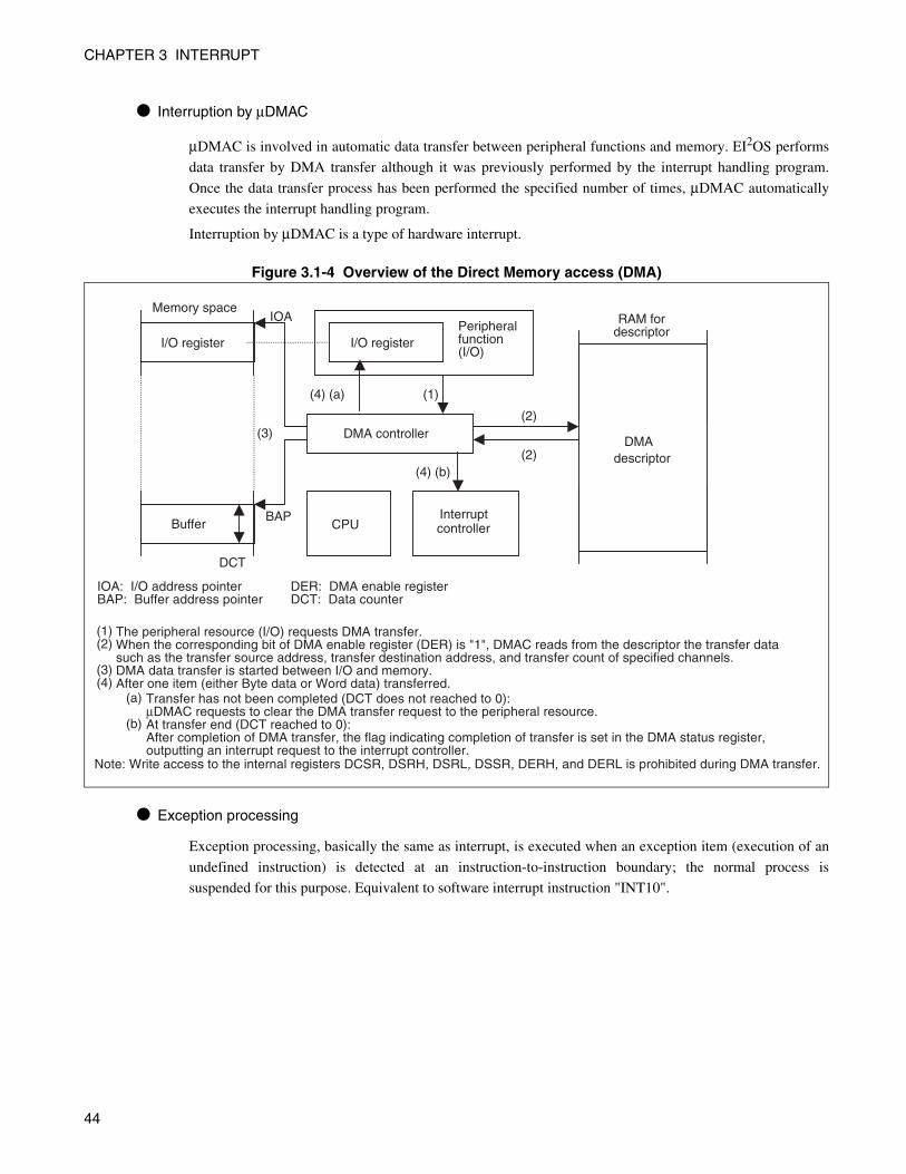
CHAPTER 3 INTERRUPT
Interruption by µDMAC
µDMAC is involved in automatic data transfer between peripheral functions and memory. EI2OS performs
data transfer by DMA transfer although it was previously performed by the interrupt handling program.
Once the data transfer process has been performed the specified number of times, µDMAC automatically
executes the interrupt handling program.
Interruption by µDMAC is a type of hardware interrupt.
Figure 3.1-4 Overview of the Direct Memory access (DMA)
Exception processing
Exception processing, basically the same as interrupt, is executed when an exception item (execution of an
undefined instruction) is detected at an instruction-to-instruction boundary; the normal process is
suspended for this purpose. Equivalent to software interrupt instruction "INT10".
I/O register
Buffer
IOA
BAP
DCT
(2)
(3) DMA controller
I/O register Peripheralfunction(I/O)
InterruptcontrollerCPU
IOA: I/O address pointerBAP: Buffer address pointer
The peripheral resource (I/O) requests DMA transfer.When the corresponding bit of DMA enable register (DER) is "1", DMAC reads from the descriptor the transfer datasuch as the transfer source address, transfer destination address, and transfer count of specified channels.DMA data transfer is started between I/O and memory.After one item (either Byte data or Word data) transferred.
(1)(2)
(3)(4)
(a)
(b)
Note: Write access to the internal registers DCSR, DSRH, DSRL, DSSR, DERH, and DERL is prohibited during DMA transfer.
Transfer has not been completed (DCT does not reached to 0):µDMAC requests to clear the DMA transfer request to the peripheral resource.At transfer end (DCT reached to 0):After completion of DMA transfer, the flag indicating completion of transfer is set in the DMA status register,outputting an interrupt request to the interrupt controller.
DER: DMA enable registerDCT: Data counter
(1)
(2)
(4) (a)
(4) (b)
Memory space
DMAdescriptor
RAM fordescriptor
44

CHAPTER 3 INTERRUPT
3.2 Interrupt Cause and Interrupt Vector
F2MC-16LX has functions that are associated with 256 types of interrupt causes, and 256 interrupt vector tables are assigned to the most significant address area of memory. This interruption vector is shared by all the interruptions.All of interrupt INT0 to INT255 are available for software interrupt, although some interrupt vectors are shared with hardware interrupt or exception processing interrupt. Furthermore, for hardware interrupt, the fixed interrupt vectors and interrupt control registers (ICR) are used for each of the peripheral functions.
Interrupt VectorThe interrupt vector table referenced during interrupt processing is assigned to the most significant of
memory address area ("FFFC00H" to "FFFFFFH"). Furthermore, the interrupt vectors share the same area
with EI2OS, µDMAC, hardware interrupt, software interrupts, and exception processing. Table 3.2-1 shows
the allocation of the interrupt numbers and interrupt vectors.
Reference:
It is recommended that the unused interrupt vectors are set in the exception processing addresses,etc.
Table 3.2-1 Interrupt Vector List
Software interrupt instruction
Vector address L
Vector address M
Vector address H
Mode dataInterrupt number
Hardware interrupt
INT0 FFFFFCH FFFFFDH FFFFFEH Unused #0 None
: : : : : : :
INT7 FFFFE0H FFFFE1H FFFFE2H Unused #7 None
INT8 FFFFDCH FFFFDDH FFFFDEH FFFFDFH #8 (RESET vector)
INT9 FFFFD8H FFFFD9H FFFFDAH Unused #9 None
INT10 FFFFD4H FFFFD5H FFFFD6H Unused #10 <Exception processing>
INT11 FFFFD0H FFFFD1H FFFFD2H Unused #11 Hardware Interrupt #0
INT12 FFFFCCH FFFFCDH FFFFCEH Unused #12 Hardware Interrupt #1
INT13 FFFFC8H FFFFC9H FFFFCAH Unused #13 Hardware Interrupt #2
INT14 FFFFC4H FFFFC5H FFFFC6H Unused #14 Hardware Interrupt #3
: : : : : : :
INT254 FFFC04H FFFC05H FFFC06H Unused #254 None
INT255 FFFC00H FFFC01H FFFC02H Unused #255 None
45

CHAPTER 3 INTERRUPT
Interrupt Factors, Interrupt Vectors, and Interrupt Control Registers
Table 3.2-2 shows the relationship between the causes of interrupts except software interrupt, and the
interrupt vectors and control registers.
Table 3.2-2 Interrupt Factors, Interrupt Vectors, and Interrupt Control Registers
Interrupt source EI2OS support
µDMACInterrupt vector Interrupt control
register Priority *2
Number Address ICR Address
Reset × × #08 08H FFFFDCH ⎯ ⎯ High
INT 9 instruction × × #09 09H FFFFD8H ⎯ ⎯
Exceptional treatment × × #10 0AH FFFFD4H ⎯ ⎯
USB Function1 × 0, 1 #11 0BH FFFFD0HICR00 0000B0H
*1
USB Function2 × 2 to 6*3 #12 0CH FFFFCCH
USB Function3 × × #13 0DH FFFFC8HICR01 0000B1H
*1
USB Function4 × × #14 0EH FFFFC4H
USB Mini-HOST1 × × #15 0FH FFFFC0HICR02 0000B2H
*1
USB Mini-HOST2 × × #16 10H FFFFBCH
I2C ch.0 × × #17 11H FFFFB8HICR03 0000B3H
*1
DTP/External interrupt ch.0/1 × #18 12H FFFFB4H
No ⎯ ⎯ #19 13H FFFFB0HICR04 0000B4H
*1
DTP/External interrupt ch.2/3 × #20 14H FFFFACH
No ⎯ ⎯ #21 15H FFFFA8HICR05 0000B5H
*1
DTP/External interrupt ch.4/5 × #22 16H FFFFA4H
PWC/Reload timer ch.0 14 #23 17H FFFFA0HICR06 0000B6H
*1
DTP/External interrupt ch.6/7 × #24 18H FFFF9CH
No ⎯ ⎯ #25 19H FFFF98HICR07 0000B7H
*1
No ⎯ ⎯ #26 1AH FFFF94H
No ⎯ ⎯ #27 1BH FFFF90HICR08 0000B8H
*1
No ⎯ ⎯ #28 1CH FFFF8CH
No ⎯ ⎯ #29 1DH FFFF88HICR09 0000B9H
*1
PPG ch.0/1 × × #30 1EH FFFF84H
No ⎯ ⎯ #31 1FH FFFF80HICR10 0000BAH
*1
PPG ch.2/3 × × #32 20H FFFF7CH
No ⎯ ⎯ #33 21H FFFF78HICR11 0000BBH
*1
No ⎯ ⎯ #34 22H FFFF74H
No ⎯ ⎯ #35 23H FFFF70HICR12 0000BCH
*1
No ⎯ ⎯ #36 24H FFFF6CH
UART (Send completed) ch.0/1 13 #37 25H FFFF68HICR13 0000BDH
*1
Extended serial I/O × 9 #38 26H FFFF64H
UART (Reception completed) ch.0/1 12 #39 27H FFFF60HICR14 0000BEH
*1
Time-base timer × × #40 28H FFFF5CH
Flash memory status × × #41 29H FFFF58HICR15 0000BFH
*1
Delay interrupt output module × × #42 2AH FFFF54H Low
46

CHAPTER 3 INTERRUPT
: Available. With EI2OS stop function. (The interrupt request flag is cleared by the interrupt clear signal. With a stop request.)
: Available. (The interrupt request flag is cleared by the interrupt clear signal.)
∆: Available when not using the interrupt factor shared with ICR
: Not available
*1: The interrupt levels for the peripheral functions sharing the ICRs are identical.
*2: The priority is given when interrupts with the same level are generated simultaneously.
*3: ch.2 and ch.3 can use even when Mini-HOST is operated.
Notes:
• If use of EI2OS is permitted when a same interrupt control register (ICR) has two interrupt causes,
EI2OS is activated when either of interrupt causes is detected. Any interrupt which is due to a
non-activation cause is masked during activation of EI2OS. It is therefore recommended that
either of the interrupt requests be masked while EI2OS is in use.
• In a resource for which two interrupt causes exist in a same interrupt control register (ICR), the
interrupt flag is cleared by the EI2OS interrupt clear signal.
• If two interrupt causes were found at a single interrupt number, both the interrupt request flags inthe resource are cleared by the µDMAC interrupt clear signal. Thus, if the µDMAC function isused for one of the two causes, the other interrupt function will not be available. Set the interruptrequest permission bit to "0" in the appropriate resource, and take measures by software pollingprocessing.
Type and Function of USB Interrupt
USB interrupt factor Details
USB function 1 End point0-IN End Point0-OUT
USB function 2 End Point1-5 *
USB function 3 SUSP SOF BRST WKUP CONF
USB function 4 SPK
USB Mini-HOST 1 DIRQ CNNIRQ URIRQ RWKIRQ
USB Mini-HOST 2 SOFIRQ CMPIRQ
*: End Point1 and End Point 2 can use even when Mini-HOST is operated.
47

CHAPTER 3 INTERRUPT
3.3 Interrupt Control Register and Peripheral Function
Interrupt control registers (ICR00 to ICR15) located in the interrupt controller, are associated with all the peripheral functions which have the interrupt function. This register controls the interrupt and the extended intelligent I/O service (EI2OS).
Interrupt Control Register ListTable 3.3-1 shows the list of the peripheral functions associated with the interrupt control registers.
Table 3.3-1 Interrupt Control Register List
Address Registers Abbreviation Corresponding peripheral function
0000B0H Interrupt control registers 00 ICR00 USB function 1 and USB function 2
0000B1H Interrupt control registers 01 ICR01 USB function 3 and USB function 4
0000B2H Interrupt control registers 02 ICR02 USB Mini-HOST 1 and USB Mini-HOST 2
0000B3H Interrupt control registers 03 ICR03 I2C ch.0, DTP External interruption ch.0/ch.1
0000B4H Interrupt control registers 04 ICR04 DTP External interruption ch.2/ch.3
0000B5H Interrupt control registers 05 ICR05 DTP External interruption ch.4/ch.5
0000B6H Interrupt control registers 06 ICR06 PWC, reload timer ch.0, DTP external interruption ch.6/ch.7
0000B7H Interrupt control registers 07 ICR07 -
0000B8H Interrupt control registers 08 ICR08 -
0000B9H Interrupt control registers 09 ICR09 PPG ch.0/ch.1
0000BAH Interrupt control registers 10 ICR10 PPG ch.2/ch.3
0000BBH Interrupt control registers 11 ICR11 -
0000BCH Interrupt control registers 12 ICR12 -
0000BDH Interrupt control registers 13 ICR13 UART transmission ch.0/ch.1 and extended serial I/O
0000BEH Interrupt control registers 14 ICR14 UART reception ch.0/ch.1, timer base timer
0000BFH Interrupt control registers 15 ICR15 Flash writing and delay interruption generation module
48

CHAPTER 3 INTERRUPT
Interrupt Control Register FunctionsEach of the interrupt control register (ICR) has the following four functions.
• Setting of interrupt level for peripheral function
• Selection of whether to perform normal interrupt or external intelligent for corresponding peripheral
function (EI2OS)
• Select the channel of Extended Intelligent I/O service (EI2OS)
• Display of extended intelligent I/O service (EI2OS) status
For the interrupt control registers (ICRs), some functions are different between write and read. Details are
shown in Figure 3.1-1 and Figure 3.1-2 in section "3.3.1 Interrupt Control Registers (ICR00 to ICR15)".
Note:
Do not use any read modify write instruction to access the interrupt control register (ICR). An attemptof this may cause a malfunction.
49

CHAPTER 3 INTERRUPT
3.3.1 Interrupt Control Registers (ICR00 to ICR15)
Interrupt control registers (ICR00 to ICR15) associated with all the peripheral functions provided with the interrupt function, controls the handling which takes place when an interrupt request is generated. Some functions of the registers are different between write and read.
Interrupt Control Registers (ICR00 to ICR15)
Figure 3.3-1 Interrupt Control Register (ICR00 to ICR15) at Writing
ICS0
At write
ISE IL1 IL0IL2
ISE
0
1
EI2OS enable bit
ICS3 ICS2 ICS1
Initial value
00000111B
IL00
1
0
1
0
1
0
1
IL10
0
1
1
0
0
1
1
IL20
0
0
0
1
1
1
1
Interrupt level 0 (Highest)
Interrupt level 7 (No interrupt)
Interrupt level set bit
000100H
000108H
000110H
000118H
000120H
000128H
000130H
000138H
000140H
000148H
000150H
000158H
000160H
000168H
000170H
000178H
0
1
2
3
4
5
6
7
8
9
10
11
12
13
14
15
00
0
0
0
0
0
0
1
1
1
1
1
1
1
1
00
0
0
1
1
1
1
0
0
0
0
1
1
1
1
00
1
1
0
0
1
1
0
0
1
1
0
0
1
1
01
0
1
0
1
0
1
0
1
0
1
0
1
0
1
ICS3 ICS2 ICS1ICS0Channel Descriptor address
EI2OS channel select bit
Address0000B0H
0000BFH
: Initial value
MSB LSB
MSB LSB
: The most significant bit: The least significant bit
Activate EI2OS during generation of an interrupt.
Activate interrupt sequence during generation of an interrupt.
to
50

CHAPTER 3 INTERRUPT
Figure 3.3-2 Interrupt Control Register (ICR00 to ICR15) at Read
S0
At read
ISE IL1 IL0IL2S1
S1
0
0
1
1
EI2OS operation in progress or EI2OS not activated
Stop status by count end
Reserved
Stop status by request from peripheral function
S0
0
1
0
1
EI2OS status
Initial value
- - 000111 B
: Undefined: Initial value
0000B0 H
0000BFH
ISE
0
1
Activate interrupt sequence during generation of an interrupt.
Activate EI2OS during generation of an interrupt.
EI2OS enable bit
IL0
0
1
0
1
0
1
0
1
IL1
0
0
1
1
0
0
1
1
IL2
0
0
0
0
1
1
1
1
Interrupt level 0 (Highest)
Interrupt level 7 (No interrupt)
Interrupt level set bit
MSB: The most significant bitLSB : The least significant bit
MSB LSBAddress
to
51

CHAPTER 3 INTERRUPT
3.3.2 Interrupt Control Register Functions
Each of the interrupt control register (ICR00 to ICR15) consists of the following bits, which have four functions.• Interrupt level set bit (IL2 to IL0)
• EI2OS enable bit (ISE)
• EI2OS channel select bits (ICS3 to ICS0)
• EI2OS status bit (S1, S0)
Configuration of Interrupt Control Register (ICR)Figure 3.3-3 shows the bit configuration of the interrupt control register (ICR).
Figure 3.3-3 Configuration of Interrupt Control Register (ICR)
References:
• ICS3 to ICS0 bit are enabled only when starting the extended intelligent I/O service (EI2OS). If
EI2OS is to be activated, set the ISE bit to "1". Otherwise, set it to "0". When you do not start
EI2OS, you can not set ICS3 to ICS0.
• ICS1 and ICS0 are enabled only for write. S1 and S0 are enabled only for read.
Note:
Reading the upper rank two-bit is an irregular value.
Writing to Interrupt control register (ICR)
ICS3 ICS2 ICS1 ICS0 ISE IL2 IL1 IL0
Initial value
Reading to Interrupt control register (ICR)
S0 ISE IL2 IL1 IL0S1
00000111B
Initial value
--000111B
Address0000B0H
0000BFH
Address0000B0H
0000BFH
: Undefiend
MSBLSB
MSB LSB
MSB LSB
: The most significant bit: The least significant bit
to
to
52

CHAPTER 3 INTERRUPT
Interrupt Control Register Functions
Interrupt level set bit (IL2 to IL0)
Specifies the interrupt level for the associated peripheral function. Initialized to level 7 (no interrupts) by
reset. Table 3.3-2 shows the relationship between the interrupt level set bits and each interrupt level.
EI2OS enable bit (ISE)
If the ISE bit is "1" during generation of an interrupt request, EI2OS is activated; if it is "0", the interrupt
sequence will be activated. Furthermore, when the end condition of EI2OS is satisfied, (both the S1 and S0
bits are other than "00B"), the ISE bit is cleared. If the associated peripheral function does not have the
EI2OS function, the ISE bit must have been set to "0" by software. The ISE bit is initialized to "0" by reset
by "0000B".
EI2OS channel select bits (ICS3 to ICS0)
Specifies the channel of EI2OS with a write only bit. The address of the EI2OS descriptor is determined by
the value set here. The ICS bit is initialized to "0000B" by reset by. Table 3.3-3 shows the correspondence
between the EI2OS channel select bits and descriptor addresses.
Table 3.3-2 Correspondence between Interrupt Level Set Bits and Interrupt Levels
IL2 IL1 IL0 Interrupt level
0 0 0 0 (highest interrupt)
0 0 1
0 1 0
0 1 1
1 0 0
1 0 1
1 1 0 6 (lowest interrupt)
1 1 1 7 (No interrupt)
53

CHAPTER 3 INTERRUPT
EI2OS status bits (S1 and S0)
It is a bit only for reading. By examining the value at the end of EI2OS operation, the operating state and/or
termination status can be determined. The bit is initialized to "00B" at a reset. Table 3.3-4 shows the
relationships between the S0/S1 bit and the EI2OS status.
Table 3.3-3 Correspondence between EI2OS Channel Select Bits and Descriptor Addresses
ICS3 ICS2 ICS1 ICS0 Channel to be selected Descriptor address
0 0 0 0 0 000100H
0 0 0 1 1 000108H
0 0 1 0 2 000110H
0 0 1 1 3 000118H
0 1 0 0 4 000120H
0 1 0 1 5 000128H
0 1 1 0 6 000130H
0 1 1 1 7 000138H
1 0 0 0 8 000140H
1 0 0 1 9 000148H
1 0 1 0 10 000150H
1 0 1 1 11 000158H
1 1 0 0 12 000160H
1 1 0 1 13 000168H
1 1 1 0 14 000170H
1 1 1 1 15 000178H
Table 3.3-4 Relation between EI2OS Status Bits and EI2OS Status
S1 S0 EI2OS status
0 0 When EI2OS in operation or not started.
0 1 Stop state by end of counting
1 0 Reserved
1 1 Stop state by request from peripheral function
54

CHAPTER 3 INTERRUPT
3.4 Hardware Interrupt
Hardware interrupt suspends the active program execution by the CPU in response to an interrupt request signal generated by a peripheral function, resulting in transfer of control to the user-defined interrupt handling program. Extended intelligent I/O service
(EI2OS), µDMAC, external interrupts, and other similar processes are also executed as a type of hardware interrupt.
Function of Hardware Interrupt
Function of hardware interrupt
Hardware interrupt makes comparison between the interrupt level of the interrupt request signal which a
peripheral function outputs and the interrupt level mask register (ILM) in the CPU's processor status (PS).
This interrupt also refers the contents of the I flag in PS, by hardware, to determine whether the interrupt is
acceptable.
Once the hardware interrupt is accepted, the contents of the registers and their related data in the CPU are
automatically saved in the system stack. The level of the currently requested interrupt is stored in the ILM.
Then, control branches to the associated interrupt vector.
Multiple interrupts
Multiple hardware interrupts can be activated.
EI2OS
At the completion of transfer, a hardware interrupt is activated although EI2OS is an automatic transfer
function between EI2OS/memory and I/O. Further, EI2OS cannot be activated in a multiple manner. While
an EI2OS process is in progress, all the other interrupt requests and µDMAC requests remain pending.
µDMAC
At the completion of transfer, a hardware interrupt is activated although µDMAC is an automatic transfer
function between memory and I/O. Further, µDMAC cannot be activated in a multiple manner. While an
µDMAC process is in progress, all the other interrupt requests and EI2OS requests remain pending.
External interrupt
The external interrupt (including a wake-up interrupt) is accepted as a hardware interrupt through the
peripheral function (its interrupt request detector circuit).
Interrupt vector
The interrupt vector table, referred during execution of the interrupt process, is assigned to the "FFFC00H"
to "FFFFFFH" memory for shared with software interrupt. For allocations of interrupt numbers and
interrupt vectors, see Section "3.2 Interrupt Cause and Interrupt Vector"
55

CHAPTER 3 INTERRUPT
Construction of Hardware InterruptAs shown in Table 3.4-1, there are four features related to hardware interrupt. These four must be
programmed when hardware interrupt is used.
Hardware Interrupt SuppressionFor hardware interrupt, acceptance of the interrupt request is suppressed in the following conditions:
Suppressing a hardware interrupt which is generated during write to a peripheral function control
register area
While data is being written to a peripheral function control register area, no hardware interrupt request is
accepted. The purpose of this is to prevent the CPU from causing a malfunction due to some interrupt-
related problem in response to an interrupt request which is generated while the interrupt control register
relation for each resource is being rewritten. The peripheral function control register area is the area
assigned to the control and data registers of the peripheral function control registers. Note that they are not
the "000000H" to "0000FFH" I/O addressing area.
Figure 3.4-1 shows the hardware interrupt operation which takes place during write to the peripheral
function control register area.
Figure 3.4-1 Hardware Interrupt Request during Write to the Peripheral Function Control Register Area
Table 3.4-1 Mechanism Related to Hardware Interrupt
Mechanism related to hardware interrupt
Functions
Peripheral functionInterrupt enable bits, interrupt request bits
Controls interrupt request from peripheral function
Interrupt controller Interrupt control registers (ICR) Setting interrupt levels
CPU
Interrupt enable flag (I) Identification of interrupt enable state
Interrupt level mask register (ILM)Compares request interrupt level and current interrupt level
Microcode Execution of interruption handling routine
"FFFC00H" to "FFFFFFH" in memory
Interrupt vector tableStores the branch destination address at interrupt processing
Instruction of writing to peripheral function control register area
Interruptprocessing
branch to interrupt
not branch to interrupt
generating interrupt request here
MOV A.#08 MOV io,A MOV A,2000H
56

CHAPTER 3 INTERRUPT
Hardware interrupt suppression of interrupt suppression instruction
Table 3.4-2 shows the hardware interrupt suppression instruction. If a hardware interrupt request is
generated during execution of the hardware interrupt suppression instruction, an interrupt is processed after
execution of the hardware interrupt suppression instruction and then other instruction.
Suppressing a hardware interrupt during execution of a software interrupt
When a software interrupt is activated, no other interrupt requests are acceptable to clear the I flag to "0".
Table 3.4-2 Hardware Interrupt Suppression Instruction
Prefix codeInterruption/holding control instruction
(The command that delays the effect of prefix code)
The instructions which do not accept
the interrupt and hold requests.
PCB DTB ADB SPB CMR NCC
MOV ILM,#imm8 OR CCR,#imm8
AND CCR,#imm8 POPW PS
57

CHAPTER 3 INTERRUPT
3.4.1 Operation of Hardware Interrupt
The following describes the operation sequence from generation of a hardware interrupt request to completion of interrupt handling.
Start of Hardware Interrupt
Operation of peripheral function (generation of interrupt request)
Any peripheral function provided with the hardware interrupt request function has "interrupt request flag"
and "interrupt enable flag". The interrupt request flag indicates whether an interrupt request has been
generated or not. The interrupt enable flag indicates whether an interrupt request is enabled or disabled.
The interrupt request flag is set by occurrence of an specific event to the peripheral function. It causes an
interrupt request to the interrupt controller when the interrupt enable flag indicates "enable".
Operation of Interrupt controller (Control of interrupt request)
The interrupt controller makes a comparison between interrupt levels (ILs) of the simultaneously received
interrupt requests. It adopts the highest-level request, (the request with the smallest IL value), and notifies it
to the CPU. If two or more requests at the same level are found, the highest priority is given to the request
with the smallest interrupt number.
CPU operation (Interrupt request acceptance and interrupt processing)
The CPU compares the received interrupt level (IL2 to IL0 of ICR) with the contents of the interrupt level
mask (ILM) register. If IL < ILM and the interrupt has been enabled (PC CCR I = 1), the currently active
instruction terminates, the interrupt handling microcode is then activated to execute the interrupt handling.
First, the interrupt handling saves the contents of the dedicated registers (12 bytes of A, DPR, ADB, DTB,
PCB, PC, and PS) in the system stack (system stack space indicated by SSB and SSP). Next, the interrupt
handling loads to the program counters (PCB and PC) of the interrupt vector, and updates the ILM. It also
sets the stack flag (S) (setting CCR S to "1" to enable the system stack).
Return from Hardware InterruptWhen the interrupt request flag of the peripheral function causing the interrupt is cleared, and the RETI
instruction is executed in the interrupt handling program, the 12-byte data saved in the system stack returns
to the dedicated registers. Control then returns to the process which was being executed before the interrupt
branch. By clearing the interrupt request flag, the interrupt request which the peripheral function has output
to the interrupt controller is canceled automatically.
58

CHAPTER 3 INTERRUPT
Operation of Hardware InterruptFigure 3.4-2 shows the operation sequence from generation of a hardware interrupt to completion of
interrupt handling.
Figure 3.4-2 Operation of Hardware Interrupt
(1)An interrupt cause occurs in a peripheral function.
(2)The peripheral function interrupt enable bit is referred. If it indicates "enable", an interrupt request is
output from the periphery to the interrupt controller.
(3)After receiving the interrupt request, the interrupt controller determines the priorities of the
simultaneously received interrupt requests. Then, the controller sends the ILs associated with the
interrupt requests to the CPU.
(4)The CPU compares the interrupt level requested from the interrupt controller with the interrupt level
mask register (ILM).
(5)If the comparison reveals that the priority is higher than the current interrupt handling level, the contents
of the I flag of the condition code register (CCR) will be checked.
(6) If the check in Item 5) reveals that the I flag indicates "enable", that is, I = 1, control waits for
completion of the currently active instruction. The requested IL is set in the ILM on completion.
(7)The contents of the register are saved before control branches to the interrupt handling routine.
(8)The software in the interrupt handling routine clears the interrupt cause generated at 1 and executes the
RETI instruction to complete the interrupt handling.
Internal bus
Microcode
Check Comparator
Other peripheral function
Levelcomparator
Interrupt level IL
Interrupt controller
Enable FF
Factor FF
IL : Interrupt level set bit of Interrupt control register (ICR)PS : Processor statusI : Interrupt enable flagILM: Interrupt level mask registerIR : Instruction registerFF : flip - flop
Peripheral function generated Interrupt request
(7)
(2)
(3)
(6)
(4)(5)
(1)
AND
PS, PC
IR
PS I ILM
F2MC-16LX CPU
(8)
RAM
59

CHAPTER 3 INTERRUPT
3.4.2 Operation Flow of Hardware Interrupt
When the peripheral function generates an interrupt request, the interrupt controller notifies the CPU of the interrupt level. If the CPU is ready to accept the interrupt, it suspends the currently active instruction; the CPU then executes the interrupt handling routine or activates Extended Intelligent I/O service (EI2OS) µDMAC. Furthermore, if a software interrupt is generated by the INT instruction, the interrupt handling routine is executed independently of the CPU state. At this time, the hardware interrupt is prohibited.
Operation Flow of Hardware InterruptFigure 3.4-3 shows the handling flow which takes place during interrupt operation.
Figure 3.4-3 Handling Flow in the Interrupt Operation
YES
START
ENx = 1
ISE = 1
YES
YES
YES
YES
NO
NO
NO
NO
NO
NO
I & IF & IE = 1AND
ILM > IL
YES
Fetch and decode next instruction
INTinstruction
Execute normal instruction
Update PC Fetch interrupt vector
Expanded intelligent I/O service processing(EI2OS processing)
I : Interrupt enable flag of Condition code register (CCR)
IF : Interrupt request flag of peripheral function
IE : Interrupt enable flag of peripheral function
ILM : CPU register level
ISE : EI2OS enable flag of Interrupt control register (ICR)
IL : Interrupt level set bit of Interrupt control register (ICR)
S : Stack flag of Condition code register (CCR)
ENx : DMA activation request flag of DMA enable register
Completionof string instruction
repetition
Saving PS, PC, PCB, DTB, DPR and A into the stack of SSP, and setting ILM=IL
Saving PS, PC, PCB, DTB, DPR and A into the stack of SSP, and setting ILM=IL
Has thespecified number
of times been completed?Or did a peripheral function
issue a completerequest?
S 1
60

CHAPTER 3 INTERRUPT
3.4.3 Procedure for Using a Hardware Interrupt
Use of hardware interrupt requires the system stack area, peripheral functions, and interrupt control registers (ICR) to be set up.
Procedure for Using a Hardware InterruptFigure 3.4-4 shows an example of the procedure for using a hardware interrupt.
Figure 3.4-4 Example of Procedure for Using a Hardware Interrupt
(1)The system stack area is set.
(2) Initialize the setting of a peripheral function which can generate an interrupt request.
(3)Set the interrupt control register (ICR) in the interrupt controller.
(4)Make the peripheral function ready to start, and set the interrupt enable bit to "enable".
(5)Sets the interrupt level mask register (ILM) and interrupt enable flag (I) to accept interrupts.
(6)Generation of an interrupt in the peripheral function generates a hardware interrupt request.
(7)The contents of the registers are saved by the interrupt handling hardware, and control branches to theinterrupt handling program.
(8)The interrupt handling program handles to the peripheral function in response to generation of theinterrupt.
(9)Clear the interrupt request from the peripheral function.
(10)Execute the interrupt return instruction to return control to the program before branching.
START
Setting System stack area
Initialize peripheral function
Setting ICR in interrupt controller
Setting ILM, I in PS
Main program
Main program
Interrupt request generation
Interrupt processing program
Branch to Stack processing interrupt vector
Clearing interrupt factor
Interrupt return instruction (RET1)
Processing by Hardware
Execution for peripheral interrupt
(execute interrupt routine)
Set the interrupt enable bit of operation
starting setting for peripheral function = enable.
(1)
(2)
(3)
(4)
(5)
(7)
(8)
(9)
(10)
(6)
61

CHAPTER 3 INTERRUPT
3.4.4 Multiple Interrupts
Multiple hardware interrupts can be implemented. To do so, set different interrupt levels for interrupt level set bits (IL0 to IL2) of the ICR in response to two or more interrupt
requests from a peripheral function. However, multiple EI2OS and multiple µDMAC cannot be started.
Multiple InterruptsIf an interrupt request with a higher interrupt level is generated during execution of the interrupt handling
routine, this higher interrupt level request is accepted with the current interrupt handling suspended. After
completion of the higher interrupt level, control returns to the handling of the suspended interrupt. The
interrupt level can be set to "0" to "7". If it is set to "7", the CPU will accept no interrupt request.
If a new interrupt at the same or a lower level is generated during execution of the current interrupt
handling, the new one remains pending until the current one is completed, unless the I flag changes the
ILM. Activation of the multiple interrupt function during the interrupt is temporarily disabled by setting the
I flag in the condition code register (CCR) to "disable" (CCR I = 0), or setting the interrupt level mask
register (ILM) to "disable" (ILM = 000B) in the interrupt handling routine.
Note:
However, multiple EI2OS and multiple µDMAC cannot be started. If an extended intelligent I/O
service (EI2OS) or µDMAC process is in progress, all the other interrupt requests and all the EI2OSand µDMAC requests remain pending.
62

CHAPTER 3 INTERRUPT
Example of Multiple InterruptsAa an example of multiple interrupt processing, set the 8/16-bit PPG timer interrupt level to 2 and the timer
interrupt level to "1", considering a case when timer interrupts are to be given higher priority than 8/16-bit
PPG timer interrupts. At this time, the handling is executed as shown in Figure 3.4-5 if a time interrupt is
generated during the 8/16-bit PPG timer handling.
Figure 3.4-5 Example of Multiple Interrupts
PPG timer Interruption generation
At the start of the PPG timer interrupt handling, the ILM is automatically set to the same value as the PPG
timer interrupt level (IL2 to IL0 in ICR). If a Level 1 or 0 interrupt request is generated, the interrupt
handling makes it a higher priority in execution.
End of interrupt processing
When the interrupt processing has completed and the return instruction (RETI) is executed, the values of
the dedicated registers (A, DPR, ADB, DTB, PCB, PC, PS) saved in the stack are returned and the interrupt
level mask register (ILM) has the values before the interrupt.
Main program PPG timer interrupt processing Timer interrupt processing
Initializeperipheral
PPG timer interruptgeneration
Main processingrestart
PPG timer interrupt processing
PPG timer interrupt return
Timer interruptgeneration
Timer interrupt processing
Timer interrupt return
Interrupt level 1(ILM=001B)
Interrupt level 2(ILM=010B)
Suspend
Restart
(1)
(7)
(8) (6) (5)
(4)
(3)
(2)
63

CHAPTER 3 INTERRUPT
3.4.5 Hardware Interrupt Processing Time
Before the interrupt handling routine can be executed after a hardware interrupt request is generated, the time to complete of the currently active instruction and the interrupt handling time are required.
Hardware Interrupt Processing TimeBefore the interrupt handling routine can be executed after an interrupt request is generated and the
interrupt is accepted, the waiting time for the interrupt request sample and the interrupt handling time
(required for preparation for interrupt handling) are required. Figure 3.4-6 shows the interrupt handling
time.
Figure 3.4-6 Interrupt Processing Time
Interrupt request sampling wait time
The wait time for an interrupt request sample refers to the time from generation of an interrupt request to
the completion of the currently active instruction. Whether or not an interrupt request is present is
determined by interrupt request sampling in the final cycle of each instruction. Because the CPU cannot
recognize the interrupt request for the above reason, the wait time is produced.
The wait time for an interrupt request sample reaches the maximum if an interrupt request is generated
immediately after the start of the PCPW, PW0,..., RW7 instructions with the longest cycle of execution (45
machine cycle).
Interrupt handling time (θ machine cycle)
The CPU must save the dedicated registers in the system stack, fetch the interrupt vectors, and execute
other processes by acceptance of the interrupt request. To do so, it requires the interrupt handling time with
the θ machine cycles. The interrupt handling time can be calculated by the expression shown below.
• When an interrupt is activated: θ = 24 + 6 x Z machine cycles
• When an interrupt is returned: θ = 11 + 6 x Z machine cycles (RETI instructions)
Normal instruction execute Interrupt handlingInterrupt processing routine
Interrupt handling time(φ machine cycle)*
Interrupt request sampling wait time
Interrupt request generation
Interrupt wait time
Operation of CPU
: The last cycle, Sampling interrupt request here: 1 machine cycle is appropriate 1 clock cycle of machine clock (φ).*
64

CHAPTER 3 INTERRUPT
The interrupt handling time depends on the address to which the stack pointer points. Table 3.4-3 shows the
compensation values (Z) of the interrupt handling time.
One machine cycle is equal to one clock cycle of the machine clock (φ).
Table 3.4-3 Compensation Value of Interrupt Handling Time (Z)
Address which stack pointer indicates Compensation value (Z)
For internal even address 0
For internal odd address +2
65

CHAPTER 3 INTERRUPT
3.5 Software Interrupt
The software interrupt function transfers control from the currently active program by the CPU to the user-defined interrupt handling program in response to execution of the software interrupt instruction (INT instruction).The hardware interrupt stops during execution of a software interrupt.
Start of Software Interrupt
Start of software interrupt
A software interrupt is started by using the INT instruction. The software interrupt request has neither the
interrupt request flag nor enable flag, execution of the INT instruction always generates a software interrupt
request.
Hardware interrupt inhibition
Because the INT instruction has no interrupt level, the interrupt level mask register (ILM) is not updated.
During the execution of an INT instruction, "0" is set in the I flag of the condition code register (CCR) to
mask hardware interrupts. To enable hardware interrupts also during software interrupt handling, set the I
flag to "1" in the software interrupt handling routine.
Operation of software interrupt
Once the CPU fetches and executes the INT instruction, the software interrupt handling microcode is
activated. With this microcode, the registers and their related data in the CPU are automatically saved in the
system stack. After hardware interrupts are masked (CCR I = 0), control branches to the associated
interrupt vector.
For allocations of interrupt numbers and interrupt vectors, see Section "3.2 Interrupt Cause and Interrupt
Vector".
Return from Software InterruptWhen the return interrupt (RETI instruction) instruction is executed in the interrupt handling program, the
12-byte data saved in the system stack returns to the dedicated registers. Control then returns to the process
which was being executed before the interrupt branch.
66

CHAPTER 3 INTERRUPT
Operation of Software InterruptFigure 3.5-1 shows the operation sequence from generation of a software interrupt to completion of
interrupt handling.
Figure 3.5-1 Operation of Software Interrupt
(1)Software interrupt instruction is executed.
(2)The required processes are performed; for example, the contents of the dedicated registers are saved
according to the microcode associated with the software interrupt instruction. The branching process is
then executed.
(3)The RETI instruction in the user-defined interrupt handling routine terminates the interrupt handling.
Precautions on Software InterruptIf the program bank register (PCB) is "FFH", the vector area for the CALLV instruction overlaps with the
table for the INT#vct8 instruction. When creating the software, pay attention to overlap of the CALLV
instruction and INT#vct8 instruction addresses.
Internal bus
(2) Microcode
Queue Fetch
PS : Processor statusI : Interrupt enable flagS : Stack flagIR : Instruction register
RAM
(1)PS, PC
IR
PS I S
67

CHAPTER 3 INTERRUPT
3.6 Interrupts by Extended Intelligent I/O Service (EI2OS)
The extended intelligent I/O service (EI2OS) executes automatic data transfer between the peripheral function (I/O) and memory. A hardware interrupt is generated at the end of the data transfer.
Extended Intelligent I/O Service (EI2OS) The extended intelligent I/O service is a kind of hardware interrupts. EI2OS executes automatic datatransfer between the peripheral function (I/O) and memory. EI2OS executes data exchange with theperipheral function (I/O), previously executed by the interrupt handling program, like direct memory access(DMA), at the end of transfer, and sets the end condition before control automatically branches to theinterrupt handling routine. The user has to write the program only about the start and end of EI2OS withouthaving to code the data transfer program between them.
Advantages of extended intelligent I/O service (EI2OS)
Compared with data transfer by the interrupt handling routine, EI2OS provides the user with the followingadvantages:
• Because no data transfer program needs to be coded, the program size can shrink.
• Because the transfer can be stopped depending the state of the peripheral function (I/O), no unnecessarydata needs to be transferred.
• Enables the user to select whether the buffer address is incremented or not updated.
• Enables the user to select whether the I/O register address is incremented or not updated.
Interrupt by extended intelligent I/O service (EI2OS) termination
After completion of data transfer by EI2OS, this sets the end condition in the S1 and S0 bits of the interruptcontrol register (ICR) before automatic branch to the interrupt handling routine.
The cause for a stop of EI2OS can be determined by checking the EI2OS status (S1 and S0 of ICR) with theinterrupt handling program.
The interrupt numbers, interrupt vectors, etc. are fixed for individual peripheral functions. For details, seeSection "3.2 Interrupt Cause and Interrupt Vector "
Interrupt control registers (ICR)
Located in the interrupt controller. Activates EI2OS, specifies the channel, and displays the at end state ofEI2OS.
Extended intelligent I/O service (EI2OS) descriptor (ISD)
Located in the 000100H to 00017FH area in RAM. Contains a set of 8-byte data used to store the transfermode, I/O address and transfer count, and buffer address. Repeated for 16 channels. Specifies the channelwith the interrupt control register (ICR).
Note:
The CPU program execution stops while the extended intelligent I/O service (EI2OS).
68

CHAPTER 3 INTERRUPT
Operation of Extended Intelligent I/O Service (EI2OS)
Figure 3.6-1 shows the operation of the EI2OS.
Figure 3.6-1 Operation of Extended Intelligent I/O Service (EI2OS)
(1) I/O demands forwarding.
(2) The interrupt controller selects the descriptor.
(3) Reads the transfer-source or transfer-destination from the descriptor.
(4) Forwarding between I/O and the memory is executed.
(5) The interruption factor is automatically clear.
CPU
I/O register
ISD
Buffer
I/O register
Interrupt control register (ICR)
Interrupt controller
Interrupt request
Peripheral function (I/O)
by IOA
by BAP
by DCT
by ICS
Memory space
(3)
(3)
(4)
(5)
(1)
ISDIOABAPICSDCT
: EI2OS descriptor: I/O address pointer: Buffer address pointer: EI2OS channel select bit for Interrupt control register (ICR): Data counter
(2)
69

CHAPTER 3 INTERRUPT
3.6.1 Extended Intelligent I/O Service (EI2OS) Descriptor (ISD)
Extended intelligent I/O service (EI2OS) descriptor (ISD) is existed to the addresses "000100H" to "00017FH" in the internal RAM and consists of 8 bytes x 16 channels.
Configuration of Extended Intelligent I/O Service (EI2OS) Descriptor (ISD)Configuration of ISD consists of 8 bytes x 16 channels, and each ISD has the configuration shown in
Figure 3.6-2. The correspondence between the channel numbers and ISD addresses is as listed in Table 3.6-1.
Figure 3.6-2 Configuration of EI2OS Descriptor (ISD)
Data counter upper 8bit (DCTH)
Data counter lower 8bit (DCTL)
I/O Register address pointer upper 8bit (IOAH)
EI2OS status register (ISCS)
I/O Register address pointer lower 8bit (IOAL)
Buffer address pointer upper 8bit (BAPH)
Buffer address pointer middle 8bit (BAPM)
Buffer address pointer lower 8bit (BAPL) ISD start address(000100H + 8 x ICS)
MSB LSB
H
L
70

CHAPTER 3 INTERRUPT
Table 3.6-1 Correspondence between Channel Numbers and Descriptor Addresses
Channel Descriptor address
0 000100H
1 000108H
2 000110H
3 000118H
4 000120H
5 000128H
6 000130H
7 000138H
8 000140H
9 000148H
10 000150H
11 000158H
12 000160H
13 000168H
14 000170H
15 000178H
71

CHAPTER 3 INTERRUPT
3.6.2 Each Register of Extended Intelligent I/O Service (EI2OS) Descriptor (ISD)
The extended intelligent I/O service (EI2OS) descriptor (ISD) consists of the following registers.• Data counter (DCT)• I/O register address pointer (IOA)
• EI2OS status register (ISCS)• Buffer address pointer (BAP)Note that resetting each register causes its initial value to be undefined.
Data Counter (DCT)Data counter (DCT), a 16-bit length register, indicates the corresponding to the transfer data count. After
each of data has been transferred, the counter is decremented by 1 (reduced value). EI2OS ends when this
counter reaches "0". Figure 3.6-3 shows the DCT configuration.
Figure 3.6-3 Configuration of Data Counter (DCT)
I/O Register Address Pointer (IOA) I/O register address pointer (IOA), a 16-bit length register, contains those low address (A15 to A0) of the
I/O register which are used for data transfer to or from the buffer. The upper address (A23 to A16)
containing all "0" data, can specify any I/O from 000000H to 00FFFFH. Figure 3.6-4 shows the IOA
configuration.
Figure 3.6-4 Configuration of I/O Register address Pointer (IOA)
B15 B14 B13 B12 B11 B10 B09 B08 B07 B06 B05 B04 B03 B02 B01 B00
Initial value
XXXXXXXXXXXXXXXXBDCT
bit12 bit11 bit9 bit8bit10bit15 bit14 bit13 bit4 bit3 bit1 bit0bit2bit7 bit6 bit5
R/WR/WR/WR/WR/WR/WR/WR/WR/WR/WR/WR/WR/WR/WR/WR/W
DCTH DCTL
R/W
X: Readable/Writable: Indeterminate
A15 A14 A13 A12 A11 A10 A09 A08 A07 A06 A05 A04 A03 A02 A01 A00
Initial value
XXXXXXXXXXXXXXXXBIOA
bit12 bit11 bit9 bit8bit10bit15 bit14 bit13 bit4 bit3 bit1 bit0bit2bit7 bit6 bit5
R/WR/WR/WR/WR/WR/WR/WR/WR/WR/WR/WR/WR/WR/WR/WR/W
IOAH IOAL
R/W
X: Readable/Writable: Indeterminate
72

CHAPTER 3 INTERRUPT
Extended Intelligent I/O Service (EI2OS) Status Register (ISCS)The extended intelligent I/O service status register (ISCS) updates or fixes the buffer address and I/O
register address pointers by the 8-bit length register. It also indicates the transfer data format (byte or word)
and the direction of transfer. Figure 3.6-5 shows the configuration of the ISCS.
Figure 3.6-5 Configuration of EI2OS Status Register (ISCS)
BW
0
1
SE
0
1It is completed by request from peripheral function.
IF BW DIR SEBF
Byte
Word
Transfer data length specification bit
Reserved
Reserved Reserved Reserved
Always set this bit to "0".
Reserved bit.
EI2OS end control bit
DIR0
1I/O register address pointer Buffer address pointer
Buffer address pointer I/O register address pointer
Data transfer direction specification bit
BF
0
1
F
0
1 Buffer address pointer is updated after transfer data. *2
I/O register pointer is not updated after transfer data.
Buffer address pointer is updated after transfer data. *1
Buffer address pointer is not updated after transfer data.
BAP update/fix selection bit
R/W : Readable/WritableX : Indeterminate
IOA update/fix selection bit
R/WR/W R/WR/W R/W R/WR/WR/W
bit7 bit6 bit5 bit4 bit3 bit2 bit1 bit0 Initial value
XXXXXXXXB
It is not completed by request from peripheral function.
*1 : Buffer address pointer is changed only lower 16-bit and enabled only increment.*2 : Address pointer is enabled only increment.
73

CHAPTER 3 INTERRUPT
Buffer Address Pointer (BAP)The buffer address pointer (BAP), a 24-bit register, contains the address used for the next attempt of
transfer by EI2OS. The BAP is provided independently for the EI2OS channels to enable the EI2OS
channels to transfer data between any address of 16 Mbytes and I/O. If the BF bit (BAP update/fix selection
bit of EI2OS status register) of the EI2OS status register (ISCS) is set to "updated", only the low order 16-
bit (BAPM, BAPL) will change in the BAP. The higher 8-bit (BAPH) will be unchanged in this case.
Figure 3.6-6 shows the BAP configuration.
Figure 3.6-6 Configuration of Buffer address Pointer (BAP)
Note:
In the I/O address pointer (IOA), the 000000H to 00FFFFH area is available for specification.
In the buffer address pointer (BAP), the 000000H to FFFFFFH area is available for specification.
The maximum transfer count which may be specified in the data counter (DCT) is 65,536 (64Kbytes).
BAPH BAPM BAPL
Initial value
XXXXXXXXXXXXXXXXXXXXXXXXBBAP
bit23 to bit16
(R/W) (R/W) (R/W) R/W : Readable/Writable
X : Indeterminate
bit15 to bit8 bit7 to bit0
74
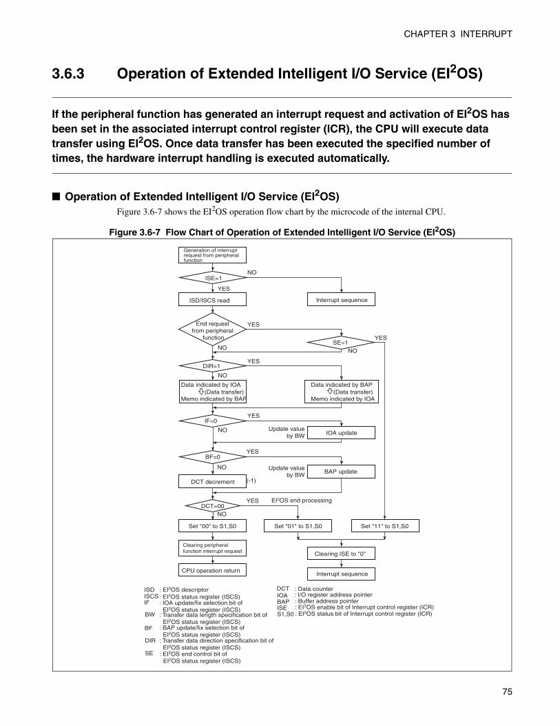
CHAPTER 3 INTERRUPT
3.6.3 Operation of Extended Intelligent I/O Service (EI2OS)
If the peripheral function has generated an interrupt request and activation of EI2OS has been set in the associated interrupt control register (ICR), the CPU will execute data transfer using EI2OS. Once data transfer has been executed the specified number of times, the hardware interrupt handling is executed automatically.
Operation of Extended Intelligent I/O Service (EI2OS)Figure 3.6-7 shows the EI2OS operation flow chart by the microcode of the internal CPU.
Figure 3.6-7 Flow Chart of Operation of Extended Intelligent I/O Service (EI2OS)
NO
NO NO
NO
NO
NO
NO
YES
YES
YES
YES
YES
YES
YES EI2OS end processing
Generation of interrupt request from peripheral function
End request from peripheral
function
ISE=1
ISD/ISCS read
Clearing peripheral function interrupt request
CPU operation return
DCT decrement
DIR=1
IF=0
BF=0
DCT=00
Interrupt sequence
Clearing ISE to "0"
Interrupt sequence
BAP update
IOA update
Set "01" to S1,S0Set "00" to S1,S0 Set "11" to S1,S0
SE=1
: EI2OS descriptorISCS : EI2OS status register (ISCS)
BW : Transfer data length specification bit of EI2OS status register (ISCS)
BF : BAP update/fix selection bit of EI2OS status register (ISCS)
DIR : Transfer data direction specification bit of EI2OS status register (ISCS)
SE : EI2OS end control bit of EI2OS status register (ISCS)
DCT : Data counterIOA
: I/O register address pointerBAP : Buffer address pointerISE : EI2OS enable bit of Interrupt control register (ICR)S1,S0 : EI2OS status bit of Interrupt control register (ICR)
(-1)
Data indicated by BAP
Memo indicated by IOA(Data transfer)
Data indicated by IOA
Memo indicated by BAP(Data transfer)
ISD
IF : IOA update/fix selection bit of EI2OS status register (ISCS)
Update valueby BW
Update valueby BW
75

CHAPTER 3 INTERRUPT
3.6.4 Procedure for Use of Extended Intelligent I/O Service (EI2OS)
To use extended intelligent I/O service (EI2OS), the system stack area, EI2OS descriptor, peripheral function, interrupt control register (ICR), and other requirements must be set up.
Procedure for Use of Extended Intelligent I/O Service (EI2OS)
Figure 3.6-8 shows the EI2OS software and the process by hardware.
Figure 3.6-8 Procedure for Use of Extended Intelligent I/O Service (EI2OS)
Setting System stack area
Setting EI2OS descriptor
Initializing Peripheral function
Setting Operation start set interrupt enable bit of internal resource
Setting ILM, I in PS
User program execution
Resetting expanded intelligent I/O service(Changing channel etc.)
Data processing during buffer
RETI
Data transfer
NO
YES
(Interrupt request)and (ISE=1)
(Branch to Interrupt vector)
ISE : EI2OS enable bit of Interrupt control register (ICR): EI2OS status of Interrupt control register (ICR)S1,S0
S1,S0="01"orS1,S0="11"
S1,S0="00"
Processing by Hardware
Initi
aliz
atio
n
Processing by Software
START
Setting Interrupt control register (ICR)
Decide whether to end counting or to branch to an interrupt by termination request from resource
76

CHAPTER 3 INTERRUPT
3.6.5 Extended Intelligent I/O Service (EI2OS) Processing Time
The time required for extended intelligent I/O service (EI2OS) processing depends on the following factors:
• Setting of EI2OS status register (ISCS)• Address (area) indicating I/O register address pointer (IOA)• Address (area) indicating buffer address pointer (BAP)• Width of external data bus when external is accessed• Data length of transfer data
Because a hardware interrupt is activated at the end of data transfer by EI2OS, the interrupt handling time will be added.
Extended Intelligent I/O Service (EI2OS) Processing Time (Time for One Transfer)
For continued data transfer
For continued data transfer, the EI2OS processing time varies with the setting in the EI2OS status register
(ISCS), as listed in Table 3.6-2.
Table 3.6-2 Extended Intelligent I/O Service Execution Time
Setting of the EI2OS termination control bit (SE)Terminated by an endrequest from periphery
Termination request from the surrounding is disregarded.
Setting of the IOA updating/fixing select bit (IF) Fixed Update Fixed Update
BAP address update/fixationSetting of selection bits (BF)
Fixed 32 34 33 35
Update 34 36 35 37
Unit: One machine cycle is equal to one clock cycle of the machine clock (φ).
77

CHAPTER 3 INTERRUPT
Further, correction may be required, depending on the condition for executing EI2OS, as shown in Table
3.6-3.
At completion of counting by data counter (DCT) (for final data transfer)
Because a hardware interrupt is activated at the end of data transfer by EI2OS, the interrupt handling time is
added. The EI2OS processing time at the end of counting is calculated by the following expression.
EI2OS processing time when count ends =
EI2OS processing time in data transfer + (21 + 6 × Z) machine cycles
↑
Interrupt handling time
The interrupt handling time depends on the address to which the stack pointer points. Table 3.6-4 shows the
compensation values (Z) of the interrupt handling time.
Table 3.6-3 Compensation Value for Data Transfer at EI2OS Processing Time
I/O register address pointerInternal Access External access
B/Even Odd B/Even 8/Odd
Buffer Address pointer
Internal AccessB/Even 0 + 2 + 1 + 4
Odd + 2 + 4 + 3 + 6
External accessB/Even + 1 + 3 + 2 + 5
8/Odd + 4 + 6 + 5 + 8
B: Byte data transfer8: External bus width 8-bit/word transferEven: Word transfer at even addressOdd: Word transfer at odd address
Table 3.6-4 Compensation Value of Interrupt Handling Time (Z)
Address which stack pointer indicates Compensation Value (Z)
At the internal even number address 0
At the internal odd number address + 2
78

CHAPTER 3 INTERRUPT
At the end caused by an end request from the peripheral function (I/O)
If data transfer by EI2OS is aborted due to an end request from the peripheral function (I/O) (ICR S1, ICR
S0 = 11), the hardware interrupt is activated without performing data transfer. The EI2OS processing time
is calculated using the expression below. Z in the expression represents the interrupt handling time
compensation value (see Table 3.6-4).
EI2OS processing time for aborted = 36 + 6 × Z machine cycles
Reference:
One machine cycle is equal to one clock cycle of the machine clock (φ).
79

CHAPTER 3 INTERRUPT
3.7 Exception Processing Interrupt
F2MC-16LX executes exception handling by executing undefined instructions. Exception handling, basically the same as interrupt, is executed when an exception item is detected during a period between instructions, the normal process is suspended for this purpose.In general, exception handling takes place as a result of unpredicted operation; it is recommended that it be used only for debugging or for activating the recovery software in the event of an emergency.
Exception Processing Interrupt
Operation of exception processing
F2MC-16LX regards as an undefined instruction any code not defined in the instruction map. When
executing an undefined instruction, F2MC-16LX performs a process equivalent to software interrupt
instruction "INT#10".
Before control branches to the interrupt routine, the exception handling performs the following processes:
1) Saving the registers of A, DPR, ADB, DTB, PCB, PC, and PS in the system stack.
2) Clearing the I flag of the condition code register (CCR) to "0" to mask the hardware interrupt.
3) Setting the S flag of the condition code register (CCR) to "1" to enable the system stack.
The program counter (PC) value saved in the system stack indicates the address storing the undefined
instruction. For any instruction code of 2 or more bytes, the PC value indicates the address which stores the
code by which the instruction has been identified as an undefined one. The PC value is useful to determine
the type of the exception cause in the exception handling routine.
Return from exception processing
After returning from the exception handling according to the RETI instruction, control starts the exception
handling again because the PC points to an undefined instruction. Some measurement such as performing a
software reset should be taken.
80

CHAPTER 3 INTERRUPT
3.8 Interruption by µDMAC
µDMAC is a simplified DMA with the same function as EI2OS.
3.8.1 µDMAC Function
3.8.2 Register of µDMAC
3.8.2.1 DMA Descriptor Channel Specification Register (DCSR)
3.8.2.2 DMA Status Register (DSRH/DSRL)
3.8.2.3 DMA Stop Status Register (DSSR)
3.8.2.4 DMA Permission Register (DERH/DERL)
3.8.3 DMA Descriptor Window Register (DDWR)
3.8.3.1 DMA Data Counter (DDCTH/DDCTL)
3.8.3.2 DMA I/O Register Address Pointer (DIOAH/DIOAL)
3.8.3.3 DMA Control Register (DMACS)
3.8.3.4 DMA Buffer Address Pointer (DBAPH/DBAPM/DBAPL)
3.8.4 Explanation of Operation of µDMAC
81

CHAPTER 3 INTERRUPT
3.8.1 µDMAC Function
µDMAC is simple DMA with the function equal with EI2OS.
µDMAC FunctionµDMAC has the following functions.
• Performs automatic data transfer between the peripheral resource (I/O) and memory.
• The program execution of CPU stops in the DMA startup.
• The DMA transfer channel is 16 channels (The smaller the channel number, the higher the priority of
DMA transfer).
• Can select either "incremented" or "not incremented" for the source or destination address.
• DMA transfer may be activated, depending on the interrupt cause by a peripheral resource (I/O).
• DMA transfer can be controlled with (a) DMA enable register (DERH/DERL), (b) DMA stop status
register (DSSR), (c) DMA status register (DSRH/DSRL), (d) DMA descriptor channel specification
register (DCSR), and descriptor (DMACS).
• A STOP request is available for stopping DMA transfer from the resource.
• After completion of DMA transfer, the flag is set in the appropriate bit of the DMA status register
(DSRH/DSRL), resulting in output of an interrupt to the interrupt controller.
82

CHAPTER 3 INTERRUPT
3.8.2 Register of µDMAC
µDMAC has four registers: DCSR, DSR, DSSR, and DER. The DMA descriptor used to set up DMA transfer is described in "3.8.3 DMA Descriptor Window Register (DDWR)".
µDMAC Register List
Figure 3.8-1 µDMA Register List
DMA descriptor channel specification register (DCSR)
DCSR
DSRH
DERH
DERL
DSRL
DMA status register (DSRH/DSRL)
DMA stop status register (DSSR)
DSSR
DSSR
DMA enable register (DERH/DERL)
00009BH STP Reserved Reserved Reserved DCSR3 DCSR2 DCSR1DCSR0
R/W R/W R/W R/W R/W R/W R/W R/W 00000000B
00009DH DTE15 DTE14 DTE13 DTE12 DTE11 DTE10 DTE9 DTE8
00009CH DTE7 DTE6 DTE5 DTE4
DTE3 DTE2 DTE1 DTE0
15 14 13 12 11 10 9 8
15 14 13 12 11 10 9 8
15 14 13 12 11 10 9 8
0000A4H
0000A4H
STP15 STP14 STP13 STP12 STP11 STP10 STP9 STP8
Initial value
R/W R/W R/W R/W R/W R/W R/W R/W Initial value
R/W R/W R/W R/W R/W R/W R/W R/W Initial value
R/W R/W R/W R/W R/W R/W R/W R/W Initial value
R/W R/W R/W R/W R/W R/W R/W R/W Initial value
R/W R/W R/W R/W R/W R/W R/W R/W Initial value
R/W R/W R/W R/W R/W R/W R/W R/W Initial value
0000ACH
0000ADH
STP7 STP6 STP5 STP4 STP3 STP2 STP1 STP0
EN15
EN14 EN13 EN12 EN11 EN10 EN9 EN8
EN7 EN6 EN5 EN4 EN3 EN2 EN1 EN0
7 6 5 4 3 2 1 0
7 6 5 4 3 2 1 0
7 6 5 4 3 2 1 0
(When STP bit of DCSR is "0" and "1", DSSR uses 8 to 15 bits and 0 to 7 bits respectively.)
00000000B
00000000B
00000000B
00000000B
00000000B
00000000B
7 6 5 4 3 2 1 0
R/W: Readable/Writable
83

CHAPTER 3 INTERRUPT
3.8.2.1 DMA Descriptor Channel Specification Register (DCSR)
DMA descriptor channel specification register (DCSR) switches the descriptor of each channel.The descriptor is set after the channel is specified by this register.
DMA Descriptor Channel Specification Register (DCSR)
Figure 3.8-2 DMA Descriptor Channel Specification Register
[bit11 to bit8] DCSRx: Specifies the DMA descriptor channel.
One descriptor channel of the 16 channels is selected by setting the DCSR. For details, see "3.8.3 DMA
Descriptor Window Register (DDWR) "
*: This function can use even when Mini-HOST is operated.
DCSR00009BH STP Reserved Reserved Reserved DCSR3 DCSR2 DCSR1 DCSR0
R/W R/W R/W R/W R/W R/W R/W R/W 00000000B
15 14 13 12 11 10 9 8
Initial value
R/W: Readable/Writable
Table 3.8-1 Relation between DCSR and Selector Channel
DCSR3 to DCSR0 Selection channel Resource interrupt request
0000B 0 USB function 1 (End Point 0-IN)
0001B 1 USB function 1 (End Point 0-OUT)
0010B 2 USB function 2 (End Point 1) *
0011B 3 USB function 2 (End Point 2) *
0100B 4 USB function 2 (End Point 3)
0101B 5 USB function 2 (End Point 4)
0110B 6 USB function 2 (End Point 5)
0111B 7 Reserved
1000B 8 Reserved
1001B 9 I/O extended serial
1010B 10 Reserved
1011B 11 Reserved
1100B 12 UART0/1, Reception
1101B 13 UART0/1, Transmission
1110B 14 PWC, reload timer 0
1111B 15 Reserved
84

CHAPTER 3 INTERRUPT
[bit15] STP:STP control bit
[bit14 to bit12] Reserved: (reserved bit)
This bit is a reserved bit.
This bit is always "0" at the beginning of reading.
Please write "0".
Note:
Do not use any read modify write (RMW) instruction to access the DCSR register.
STP bit Function
0 [Initial value] STP8 to STP15 is selected as DSSR.
1 STP0 to STP7 is selected as DSSR.
85

CHAPTER 3 INTERRUPT
3.8.2.2 DMA Status Register (DSRH/DSRL)
DMA status register (DSRH/DSRL) indicates that the DMA transfer ended. When "1" is set to this register, the interrupt is generated at the same time.
Bit Configuration of DMA Status Register (DSRH/DSRL)
Figure 3.8-3 Bit Configuration of DMA Status Register (DSRH/DSRL)
[bit15 to bit0] DTEx: DMA Status
Note:
To write data to the DSRH/DSRL, use a read-modify-write (RMW) instruction.
DSRH
DSRL
00009DH DTE15 DTE14 DTE13 DTE12
DTE11 DTE10 DTE9 DTE8
00009CH DTE7 DTE6 DTE5
DTE4
DTE3
DTE2
DTE1 DTE0
15 14 13 12 11 10 9 8
R/W R/W R/W R/W R/W R/W R/W R/W 00000000BInitial value
R/W R/W R/W R/W R/W R/W R/W R/W 00000000BInitial value7 6 5 4 3 2 1 0
R/W: Readable/Writable
DTEx bit Function
0 [Initial value]The DMA transfer has not ended.Please write "0" when DTEx is "0".
1Indicates that DMA transfer was completed and an interrupt request is being executing.The DMA transfer due to the STOP request except last transfer does not set 1 to this bit.When DTEx is "1", writing "0" clears it to "0" and writing "1" holds the previous data.
86

CHAPTER 3 INTERRUPT
3.8.2.3 DMA Stop Status Register (DSSR)
DMA stop status register (DSSR) indicates that the DMA transfer stopped due to the STOP request. The meaning of the bit in this register is different depending on the STP bit of the DMA descriptor channel specification register (DCSR).
DMA Stop Status Register (DSSR)
Figure 3.8-4 Bit Configuration of DMA Stop Status Register (DSSR)
[bit15 to bit0] STPx: DMA stop status
The following one channel corresponds to the STOP demand.
Bits other than STP12 does not have the meaning.
DSSR
DSSR
0000A4H
0000A4H
STP15 STP14 STP13 STP12 STP11 STP10 STP9 STP8
R/W R/W R/W R/W R/W R/W R/W R/W 00000000BInitial value
R/W R/W R/W R/W R/W R/W R/W R/W 00000000BInitial value
STP7 STP6
STP5 STP4 STP3 STP2 STP1 STP0
7 6 5 4 3 2 1 0
DCSR STP bit = 0
DCSR STP bit = 1
7 6 5 4 3 2 1 0
R/W: Readable/Writable
STPx bit Function
0 [Initial value]During DMA transfer, no STOP request is accepted from the resource.Please write "0" at STPx=0.
1
During DMA transfer, indicates that DMA transfer stopped in response to a STOP request from theresource. However, "1" is not set to STOPx bit even though the STOP request is accepted at last transfer.If the SE bit of DMA control register is "1" and a STOP request is received by the associated channel,the corresponding bit of the DMA permission register is cleared to "0". When STPx = 1, writing "0" clears it to "0" and writing "1" holds the previous data.
Channel Corresponding STPx bit Resource
ch.12 STP12 UART0/1, Reception
87

CHAPTER 3 INTERRUPT
Notes:
• DSSR is controlled by most significant bit (STP) of DCSR. If STP is "0", bit8 to bit15 will beselected as being used for the DSSR. If it is "1", bit0 to bit7 will be used for the DSSR. Becausethe initial value of STP is "0", bit8 to bit15 is initially selected.
• To write data to the DSSR, use a read modify write (RMW) instruction.
88

CHAPTER 3 INTERRUPT
3.8.2.4 DMA Permission Register (DERH/DERL)
DMA enable register (DERH/DERL) enables the DMA transfer. When "1" is set to this register, the interrupt request, which is the DMA transfer request, generates to the corresponding channel, and starts the DMA transfer.
DMA Enable Register (DERH/DERL)
Figure 3.8-5 Bit Configuration of DMA Enable Register (DERH/DERL)
[bit15 to bit0] ENx: DMA permission
Notes:
• To write data to the DERH/DERL, use a read modify write (RMW) instruction.
• Before changing the mode to the standby mode (sleep mode, stop mode, watch mode, andtimebase timer mode) or the CPU intermittent operation mode (main clock intermittent operationmode, PLL clock intermittent mode, and sub-clock intermittent mode), the DMA enable registermust be set to "0".
DERH
DERL
15 14 13 12 11 10 9 8
R/W R/W R/W R/W R/W R/W R/W R/W 00000000BInitial value
R/W R/W R/W R/W R/W R/W R/W R/W 00000000BInitial value
0000ACH
0000ADH EN15 EN14 EN13 EN12 EN11 EN10 EN9 EN8
EN7 EN6 EN5 EN4 EN3 EN2 EN1 EN0
7 6 5 4 3 2 1 0
R/W: Readable/Writable
ENx bit Function
0 [Initial value] This bit does not execute the DMA transfer.
1
The interrupt request from the resource is handled as a DMA activation request, and the interruptrequest is output to the interrupt controller at the end of DMA transfer.When the number of DMA transfer bytes reaches 0, or a STOP request from the resource stops DMAtransfer, this is cleared to "0".
89

CHAPTER 3 INTERRUPT
3.8.3 DMA Descriptor Window Register (DDWR)
The DMA descriptor, consisting of 8 bytes × 16 channels, is used to set up DMA transfer. One of the 16 channels is specified, and mapped to the DMA descriptor window register (DDWR) for being accessible. The address of DDWR is 007920H to
007927H.
Configuration of DMA Descriptor Window Register (DDWR)The DMA descriptor consists of 8 bytes × 16 channels. The configuration of each channel is shown in
Figure 3.8-6. The descriptor of the channel selected by the DMA descriptor channel specification register
(DCSR) or interrupt request channel number is mapped to the DMA descriptor window register (DDWR).
See Table 3.8-1 for the relationship between the DMA descriptor channel specification register (DCSR)
and the selected channel.
Figure 3.8-6 Configuration of DMA Descriptor Window Register (DDWR)
Each Register of DMA DescriptorEach register configuring the DMA descriptor is described in the following pages. The initial value of each
register is made undefined when a reset is generated. Thus, make sure that the initialization has finished
before ENx is set to "1".
Note:
If the DCSR is used to switch the channel descriptor, access to DDWR is inhibited during the 2subsequent machine cycles.
Address
DMA Data counter upper 8-bit (DDCTH)
DMA Buffer address pointer upper 8-bit (DBAPH)
DMA Buffer address pointer middle 8-bit (DBAPM)
DMA Buffer address pointer lower 8-bit (DBAPL)
DMA Data counter lower 8-bit (DDCTL)
DMA I/O register address pointer upper 8-bit (DIOAH)
DMA I/O register address pointer lower 8-bit (DIOAL)
DMA Control register (DMACS)
007927H
007926H
007925H
007924H
007923H
007922H
007921H
007920H
90

CHAPTER 3 INTERRUPT
3.8.3.1 DMA Data Counter (DDCTH/DDCTL)
DMA data counter (DDCTH/DDCTL) sets the data transfer. When DDCTH/DDCTL is 0, the DMA transfer ends.
DMA Data Counter (DDCTH/DDCTL) DMA data counter (DDCTH/DDCTL), a 16-bit length register, indicates the counter associated with
transferred number. After each data has been transferred, the counter is always decremented by 1 regardless
of transferred data (word or byte). The DMA transfer ends when this counter reaches 0. Figure 3.8-7 shows
the DDCT configuration.
If the DDCT is set to "0", the maximum data transfer count (65536) is set.
Figure 3.8-7 Bit Configuration of DMA Data Counter (DDCTH/DDCTL)
About the Set Value of DMA Data Counter (DDCTH/DDCTL)Table 3.8-2 shows the relationship between the number of transferred bytes and the DDCTH/DDCTL.
Initial value
R/W: Readable/WritableX: Indeterminate
R/W R/W R/W R/W R/W R/W R/W R/W R/W R/W R/W R/W R/W R/W R/W R/W
bit15 bit10 bit7 bit0bit1bit2bit3bit5 bit4bit6bit8bit12bit13bit14 bit9bit11DDCTH/DDCTL B15 B01B02B03B04B05B07 B06B08B09B10B13B14 B00B11B12 XXXXXXXXXXXXXXXXB
007927H/007926H DDCTH DDCTL
Table 3.8-2 Set Value of DMA Data Counter (DDCTH/DDCTL)
DMACS DDCT
BW bit BYTEL bit
0 - N
1 0 N/2
1 1 (N+1)/2
N: Number of transfer bytes
91

CHAPTER 3 INTERRUPT
3.8.3.2 DMA I/O Register Address Pointer (DIOAH/DIOAL)
DMA I/O register address pointer (DIOAH/DIOAL) sets the I/O address pointer. The upper address (A23 to A16) is fixed at "00H".
DMA I/O Register Address Pointer (DIOAH/DIOAL)The DMA I/O register address pointer (DIOAH/DIOAL), a 16-bit length register, indicates the 16 low
order bits (A15 to A00) of the DMA I/O register address. The upper-level address (A23 to A16), containing
all "0" data, can specify any I/O address space from 000000H to 00FFFFH. If the IF bit (DIOA update/fix
selection bit) of the DMA control register (DMACS) is set to "updated", the DIOAH/DIOAL will be
incremented by 1 during byte transfer or by 2 during word transfer. If this bit is set to "not updated", the
DIOAH/DIOAL will be fixed. Figure 3.8-8 shows the DIOA configuration.
Figure 3.8-8 Bit Configuration of DMA I/O address Register Pointer (DIOAH/DIOAL)
Initial valueInitial value
R/W: Readable/WritableX: Indeterminate
R/W R/W R/W R/W R/W R/W R/W R/W R/W R/W R/W R/W R/W R/W R/W R/W
bit15 bit10 bit7 bit0bit1bit2bit3bit5 bit4bit6bit8bit12bit13bit14 bit9bit11DIOAH/DIOAL
A15 A01A02A03A04A05A07 A06A08A09A10A13A14 A00A11A12 XXXXXXXXXXXXXXXXB
007925H/007924H DIOAH DIOAL
92

CHAPTER 3 INTERRUPT
3.8.3.3 DMA Control Register (DMACS)
DMA control register (DMACS) controls the DMA transfer.The following can be controlled by the DMACS.
• Direction control (IOA → BAP and BAP→ IOA)• Transfer bit length (Byte and word)• Address update (provided or not provided)• Transfer interval• Odd-numbered byte control at word transfer
DMA Control Register (DMACS) The DMA control register (DMACS), an 8 bit length specifies update/fix, the transfer data format (byte or
word), the direction of transfer, and byte transfer, and issues a wait instruction of DMA buffer address
pointer and DMA I/O register address pointer. Figure 3.8-9 shows the DMACS configuration.
Figure 3.8-9 Bit Configuration of DMA Control Register (DMACS)
It is completed by request from peripheral function.
Byte
Word
Transfer data length specification bit
DMA I/O register address pointer DMA Buffer address pointer
DMA Buffer address pointer DMA I/O register address pointer
Data transfer direction specification bit
After data transfer, the I/O register address pointer is updated.
After data transfer, the I/O register address pointer is not updated.
After data transfer, the buffer address pointer is updated.
After data transfer, the buffer address pointer is not updated.
BAP update/fix selection bit
R/W: Readable/WritableX : Indeterminate
IOA update/fix selection bit
Initial valueAddress
It is not completed by request from peripheral function.
DMA transfer end control bit
Wait instruction bits (see Figure 8-10)(RDY2, RDY1)
(0, 0)
(0, 1)
(1, 0)
(1, 1)
No wait is inserted between transfers.
A 1-cycle wait is inserted between transfers.
Byte transfer specification bit (only enabled for word transfer)
Odd number of Bytes
Even number of Bytes
A 2-cycle wait is inserted between transfers.
A 3-cycle wait is inserted between transfers.
BYTEL
0
1
0
1
0
1
BW
IF
0
1
DIR
0
1
BF
0
1
SE
XXXXXXXXB
R/W R/W R/W R/WR/WR/WR/W R/W
007923H
bit7 bit6 bit1bit2bit3bit5 bit4 bit0
RDY2 RDY1 BYTEL SEDIRBFBWIF
93

CHAPTER 3 INTERRUPT
Figure 3.8-10 Wait Specification Bit Explanation
Note:
If writing transmission data to UART by using µDMAC, not setting RDY2 and RDY1 bit of DMACSregister in (0, 0).
source destination wait source destination
Length of wait part in transfer such as above
figure is defined by RDY2 and RDY1.
94

CHAPTER 3 INTERRUPT
3.8.3.4 DMA Buffer Address Pointer (DBAPH/DBAPM/DBAPL)
DMA buffer address pointer (DBAPH/DBAPM/DBAPL) sets the buffer address pointer.The DBAPH/DBAPM/DBAPL can be set A23 to A00.
DMA Buffer Address Pointer (DBAPH/DBAPM/DBAPL)The DMA buffer address pointer (DBAPH/DBAPM/DBAPL), a 24-bit register, contains the address used
for DMA transfer. DBAP are provided independently for the DMA channels to enable the DMA channels
to transfer data between any address of 16 Mbytes and I/O. If the BF bit (DBAP update/fix selection bit) of
the DMA control register (DMACS) is set to "updated", the 16 lower order bits (DBAPM, DBAPL) of the
DBAP will be incremented by 1 during byte transfer or by 2 during word transfer. The 8 high order bits
(DBAPH) will be unchanged in this case Figure 3.8-11 shows the DBAP configuration.
Figure 3.8-11 Bit Configuration of DMA Buffer address Pointer (DBAPH/DBAPM/DBAPL)
Notes:
• In the DMA I/O register address pointer (DIOAH/DIOAL), the 000000H to 00FFFFH area isavailable for specification.
• In the DMA buffer address pointer (DBAPH/DBAPM/DBAPL), the 000000H to FFFFFFH area isavailable for specification.
• µDMAC internal register DCSR, DSRH, DSRL, DSSR, DERH, or DERL, or an address of DMAdescriptor window register (DDWR) may not be specified in the DIOA or DBAP.
: Readable/Writable: Indeterminate
Initial value
XXXXXXXXXXXXXXXXXXXXXXXXB
007922H, 007921H, 007920H
bit23 bit16 bit15 bit8 bit7 bit0DBAPH/DBAPM/DBAPL
DBAPH DBAPM DBAPL
R/W R/W R/W
R/WX
95
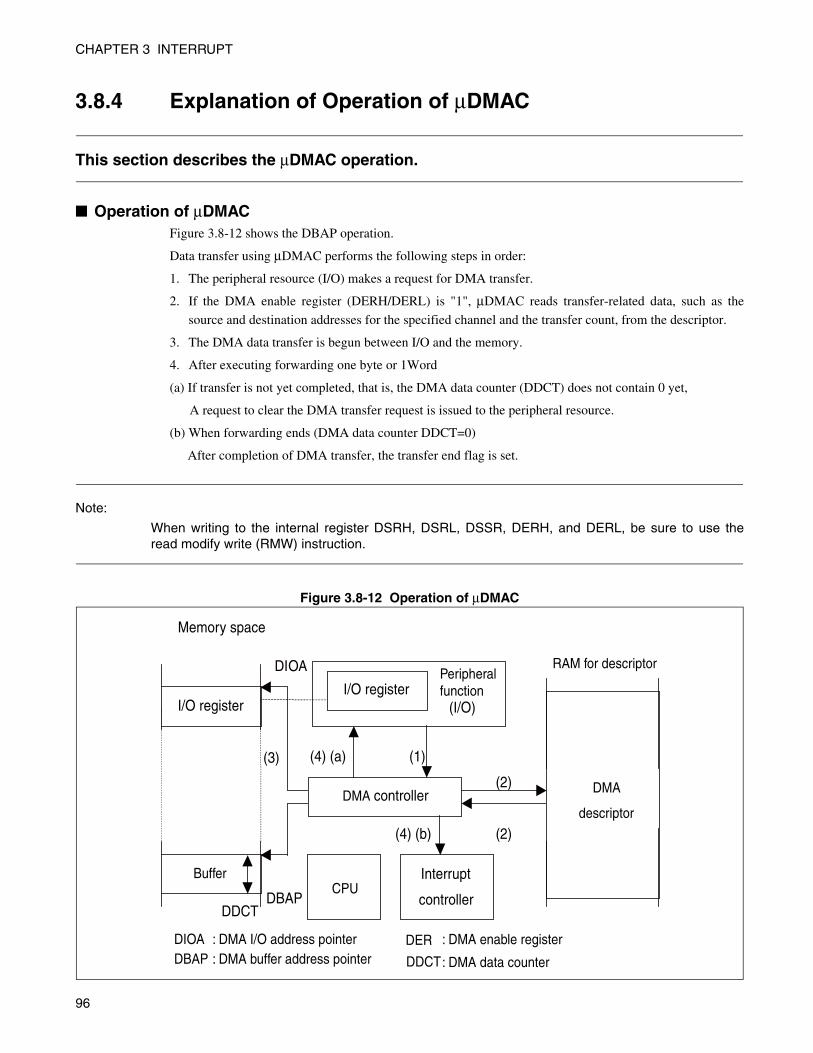
CHAPTER 3 INTERRUPT
3.8.4 Explanation of Operation of µDMAC
This section describes the µDMAC operation.
Operation of µDMACFigure 3.8-12 shows the DBAP operation.
Data transfer using µDMAC performs the following steps in order:
1. The peripheral resource (I/O) makes a request for DMA transfer.
2. If the DMA enable register (DERH/DERL) is "1", µDMAC reads transfer-related data, such as the
source and destination addresses for the specified channel and the transfer count, from the descriptor.
3. The DMA data transfer is begun between I/O and the memory.
4. After executing forwarding one byte or 1Word
(a) If transfer is not yet completed, that is, the DMA data counter (DDCT) does not contain 0 yet,
A request to clear the DMA transfer request is issued to the peripheral resource.
(b) When forwarding ends (DMA data counter DDCT=0)
After completion of DMA transfer, the transfer end flag is set.
Note:
When writing to the internal register DSRH, DSRL, DSSR, DERH, and DERL, be sure to use theread modify write (RMW) instruction.
Figure 3.8-12 Operation of µDMAC
DER
DDCT
I/O register
Buffer
DIOA
DBAP DDCT
(2)
(3)
DMA controller
Peripheralfunction
(I/O) I/O register
Interrupt
controllerCPU
(1)
(2)
(4) (a)
(4) (b)
DIOA : DMA I/O address pointer
DBAP : DMA buffer address pointer
Memory space
DMA
descriptor
RAM for descriptor
: DMA enable register
: DMA data counter
96
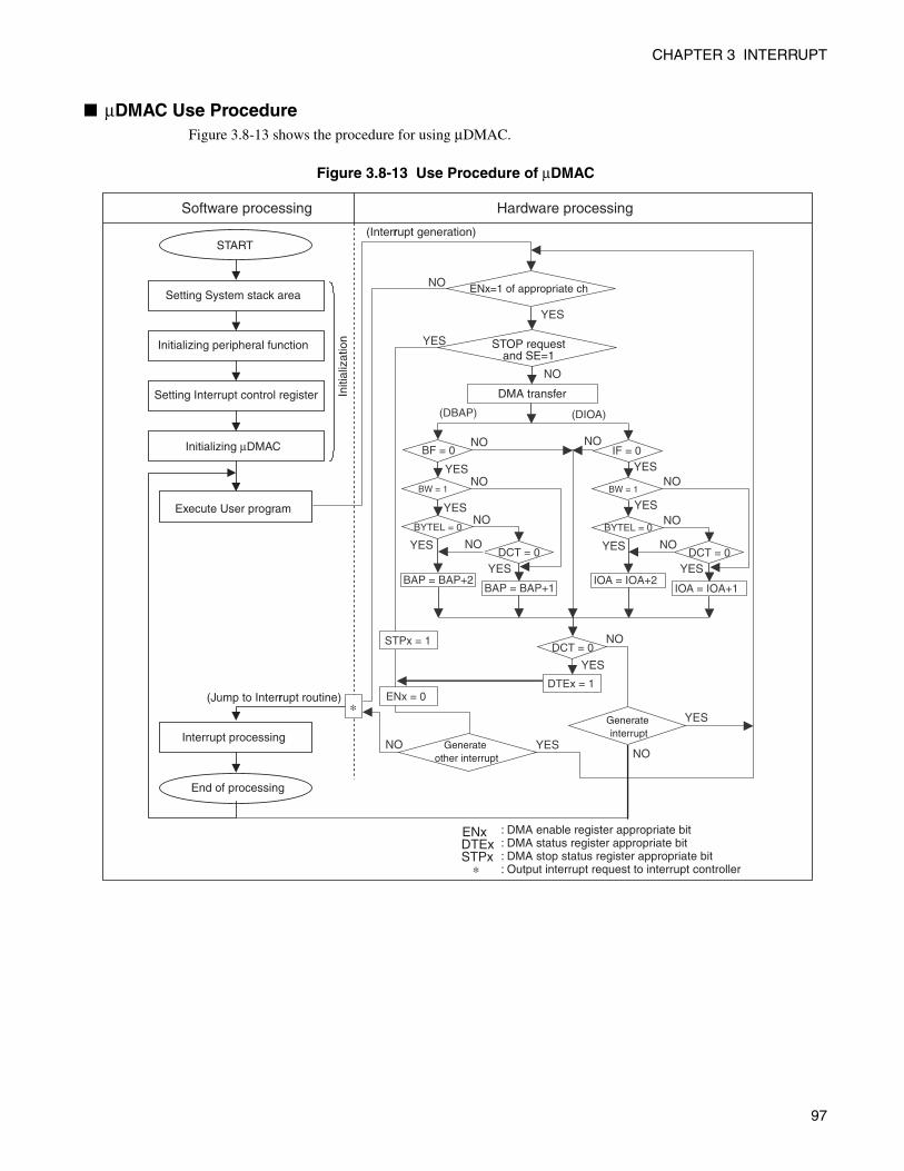
CHAPTER 3 INTERRUPT
µDMAC Use ProcedureFigure 3.8-13 shows the procedure for using µDMAC.
Figure 3.8-13 Use Procedure of µDMAC
NO
BF = 0
DCT = 0
STPx = 1
ENx = 0
BAP = BAP+2
BW = 1
BYTEL = 0
BAP = BAP+1
IF = 0
DCT = 0
IOA = IOA+2
BW = 1
BYTEL = 0
IOA = IOA+1
DCT = 0
(DBAP) (DIOA)
DTEx = 1
Software processing Hardware processing
(Interruptr generation)START
Setting System stack area
Initializing peripheral functionIn
itial
izat
ion
Setting Interrupt control register
Execute User program
DMA transfer
STOP requestand SE=1
(Jump to Interruptr routine)
Interrupt processing
End of processing
: DMA enable register appropriate bit: DMA status register appropriate bit: DMA stop status register appropriate bit: Output interrupt request to interrupt controller
ENx=1 of appropriate ch
ENxDTExSTPx
Generate other interrupt
Generate interrupt
YES
YES
NO
NO
NO
NO
NO YES
YES
YESNO
NO
YES
YES
YES
YES
NO
NO
NO
NO
NO
YES
YES
YES
YES
97

CHAPTER 3 INTERRUPT
3.9 Exceptions
The F2MC-16LX performs exception processing when the following event occurs.
Execution of an Undefined InstructionException processing is fundamentally the same as interrupt processing. When an exception is detected
between instructions, exception processing is performed separately from ordinary processing. In general,
exception processing is performed as a result of an unexpected operation. Fujitsu recommends using
exception processing only for debugging or for activating emergency recovery software.
Exception due to Execution of an Undefined Instruction
The F2MC-16LX handles all codes that are not defined in the instruction map as undefined instructions.
When an undefined instruction is executed, processing equivalent to the INT 10 software interrupt
instruction is performed. Specifically, the AL, AH, DPR, DTB, ADB, PCB, PC, and PS values are saved
into the system stack, and processing branches to the routine indicated by the interrupt number 10 vector. In
the undefined instruction is stored. Processing can be restored by the RETI instruction, but is of no use,
however, because the same exception occurs again.
98

CHAPTER 3 INTERRUPT
3.10 Stack Operation of Interrupt Processing
Once an interrupt is accepted, the contents of the dedicated registers are automatically saved in the system stack before control branches to the interrupt handling. Return from the stack at the end of the interrupt handling also takes place automatically.
Stack Operation at the Start of Interrupt ProcessingOnce the interrupt is accepted, the CPU automatically saves the contents of the current dedicated registers
and their related data in the system stack in the order below:
1. Accumulator (A)
2. Direct page register (DPR)
3. Additional data bank register (ADB)
4. Data bank register (DTB)
5. Program bank register (PCB)
6. Program counter (PC)
7. Processor status (PS)
Figure 3.10-1 shows the stack operation at the start of interrupt handling.
Figure 3.10-1 Stack Operation at Start of Interrupt Processing
Stack Operation when Interrupt Processing ReturnsWhen the interrupt return instruction (RETI) is executed at the end of interrupt process, the values of PS,
PC, PCB, DTB, ADB, DPR, and A return from the stack in the reverse order for the start of interrupt
handling. The dedicated registers are restored to the initial state preceding the start of interrupt.
SSB
SSP
A
DPR
DTB
PC
PS
ADB
PCB
AH AL
SPH
L
SSB
SSP
A
DPR
DTB
PC
PS
ADB
PCB
AH AL
SP
AH
AL
DPRADBDTBPCB
PC
PS
08FFH
08FEH
08F2H
08FFH
0000H
803FH
20E0H
08FEH
08FEH
00H
00H
00H
FFH
01H
0000H
803FH
20E0H
08FEH
08F2H
00H
00H
00H
FFH
01H
XXH
XXH
XXH
XXH
XXH
XXH
XXH
XXH
XXH
XXH
XXH
XXH
00H
00H
08H
FEH
01H
00H
00H
FFH
80H
3FH
20H
E0H
08FEH
08F2H
Byte Byte
SP after updated
MemoryAddressMemoryAddressPreviously interrupt Immediately interrupt
99

CHAPTER 3 INTERRUPT
Stack Area
Securing stack area
The stack area is used to save or return the program counter (PC) used to execute the subroutine call
(CALL) or vector call (CALLV) instruction as well as execute the interrupt handling. This area is also
used, by the PUSHW or POPW instruction, to save or return the contents of temporary registers and their
related data. The stack area is located in RAM together with the data area.
Figure 3.10-2 shows the stack area.
Figure 3.10-2 Stack Area
Notes:
• As a general rule, even addresses should be set in the stack pointers (SSP and USP).
• The system stack area, user stack area, and data area should not overlap.
System stack area and user stack area
The system stack area is used for interrupt processing. Even if the user stack area is being used, generation
of an interrupt causes forcible switching to the system stack. For this reason, the system stack area must
have been set up properly even in a system where the user stack area is primarily used. In particular, only
the system stack area should be used unless it is necessary to divide the stack space.
Vector table(Reset, Interrupt vector call instruction)
ROM area
Internal I/O area
Internal RAM area
General-purpose register
bank area
Stack area
*2: Built-in RAM capacity is difference depending on products.*1: Built-in ROM capacity is difference depending on products.
000000H
FFFFFFH
FFFC00H
FC0000H*1
0040FFH*2
000380H
000180H
000100H
0000FBH
100

CHAPTER 3 INTERRUPT
3.11 Program Example of Interrupt Processing
An example of interrupt processing program is shown below.
Program Example of Interrupt Processing
Processing specification
An example interruption program that uses external interruption 0 (INT0)
Coding example
DDR6 EQU 000016H ; Port 6 direction register
ENIR EQU 00003CH ; Interruption/DTP permission register
EIRR EQU 00003DH ; Interruption/DTP factor register (EIRR)
ELVR EQU 00003EH ; A register to specify the required level
ICR03 EQU 0000B3H ; Interrupt control register 03
STACK SSEG ; Stack
RW 100
STACK_T RW 1
STACK ENDS
;----------Main Program------------------------------------------------------------
CODE CSEG ;
START:
MOV RP, #0 ; Header bank used for general-purpose registers
MOV ILM, #07H ; Sets ILM in PS to level 7
MOV A, #!STACK_T ; Sets system stack
MOV SSB, A
MOVW A, #STACK_T ; Setting of stack pointer, in this case,
MOVW SP, A ; S flag = 1, so set to SSP
MOV DDR6,#00000000B ; Sets the P60/INT0 pin for input
OR CCR, #40H ; Sets I flag of CCR in PS to enable interrupts.
MOV I:ICR03, #00H ; It is assumed interrupt levels 0(Max)
MOV I:ELVR, #00000001B ; Make INT0 "H" level request
MOV I:EIRR, #00H ; Clears interrupt cause for INT0.
MOV I:ENIR, #01H ; INT0 input permitted
:
LOOP: NOP ; Dummy loop
NOP
NOP
101
CHAPTER 3 INTERRUPT
NOP
BRA LOOP ; Unconditional jump
;----------Interrupt Program------------------------------------------------------------
ED_INT1:
MOV I:EIRR, #00H ; New acceptance of INT0 prohibited
NOP
NOP
NOP
NOP
NOP
NOP
RETI ; Returns from interrupt.
CODE ENDS
;----------Vector Settings------------------------------------------------------------------
VECT CSEG ABS=0FFH
ORG 0FFB4H ; The vector is set in interruption #18(12H)
DSL ED_INT1
ORG 0FFDCH ; Reset vector setting
DSL START
DB 00H ; Single-chip mode setting
VECT ENDS
END START
Processing specification for program example of extended intelligent I/O service (EI2OS)
1. The extended intelligent I/O service (EI2OS) is started upon detection of the "H" level signal which
inputs to the INT0 pin.
2. When "H" level is input to INT0 pin, EI2OS is started, which transfers data at port 0 to memory address
"3000H".
3. The number of transfer data bytes is 100. After the 100 bytes have been transferred, an interrupt is
generated because of completion of EI2OS data transfer.
102

CHAPTER 3 INTERRUPT
Coding example
DDR6 EQU 000016H ; Port 6 direction register
ENIR EQU 00003CH ; Interruption/DTP permission register
EIRR EQU 00003DH ; Interruption/DTP factor register
ELVR EQU 00003EH ; A register to specify the required level
ICR03 EQU 0000B3H ; Interrupt control registers 03
BAPL EQU 000100H ; Buffer address pointer lower
BAPM EQU 000101H ; Buffer address pointer middle
BAPH EQU 000102H ; Buffer address pointer upper
ISCS EQU 000103H ; EI2OS Status
IOAL EQU 000104H ; Lower I/O address pointer
IOAH EQU 000105H ; Higher I/O address pointer
DCTL EQU 000106H ; Data counter lower
DCTH EQU 000107H ; Data counter upper
ER0 EQU EIRR:0 ; Defines external interrupt request flag bit.
STACK SSEG ; Stack
RW 100
STACK_T RW 1
STACK ENDS
;----------Main Program------------------------------------------------------------
CODE CSEG
START:
AND CCR,#0BFH ; Clears the I flag of CCR in PS to disable interrupts.
MOV RP,#00 ; Sets register bank pointer.
MOV A,#!STACK_T ; Sets system stack
MOV SSB,A
MOVW A,#STACK_T ; Setting of stack pointer, in this case,
MOVW SP,A ; S flag = 1, so set to SSP
MOV I:DDR6,#00000000B ; Sets the P60/INT0 pin for input.
MOV BAPL,#00H ; Sets buffer address (003000H)
MOV BAPM,#30H
MOV BAPH,#00H
MOV ISCS,#00010001B ; No I/O address update, byte transfer
Buffer address updated
; The peripheral function terminates I/O to buffer
transfer.
Yes
MOV IOAL,#00H ; Sets transfer source address (port 0: 000000H)
MOV IOAH,#00H
103

CHAPTER 3 INTERRUPT
MOV DCTL,#64H ; Sets transfer byte count (100 bytes)
MOV DCTH,#00H
MOV I:ICR00,#00001000B ; EI2OS ch.0, EI2OS enable, interrupt level 0 (highest)
MOV I:ELVR,#00000001B ; Make INT0 "H" level request
MOV I:EIRR,#00H ; Clears interrupt cause for INT0.
MOV I:ENIR,#01H ; Enables INT0 interrupt.
MOV ILM,#07H ; Sets ILM in PS to level 7
OR CCR,#40H ; Sets I flag of CCR in PS to enable interrupts.
:
LOOP: BRA LOOP ; Infinite loop
;----------Interrupt Program------------------------------------------------------------
WARI CLRB ER0 ; Interrupt/DTP request flag clear
:
user processing ; confirmation of the cause of the EI2OS completion
: ; Processes data in buffer, resetting EI2OS etc.
RETI
CODE ENDS
----------Vector Settings-------------------------------------------------------------------
VECT CSEG ABS=0FFH
ORG 0FFB4H ; The vector is set in interruption #18(12H).
DSL WARI
ORG 0FFDCH ; Reset vector setting
DSL START
DB 00H ; Single-chip mode setting
VECT ENDS
END START
104

CHAPTER 3 INTERRUPT
3.12 Delayed Interrupt Generation Module
The delayed interrupt generation module is used to generate a task switching interrupt.
Use of this module enables F2MC-16LX CPU to generate or cancel an interrupt request.
Block Diagram of Delayed Interrupt Generation ModuleFigure 3.12-1 shows the block diagram of the delayed interrupt generation module.
Figure 3.12-1 Block Diagram of Delayed Interrupt Generation Module
List of Register of Delay Interruption Generation ModuleThe register configuration of the delayed interrupt generation module delayed interrupt cause generation/
clear register (delayed interrupt request register (DIRR)) is shown in the following figure.
Figure 3.12-2 Delayed Interrupt Cause Generation/clear Register (DIRR)
Delay interruption factor generation/release register (DIRR) controls the delay factor generation and
release. Writing "1" to this register generates a delayed interrupt request. Writing "0" to it resets the
request. A reset causes the state cause to remain cleared. Either "0" or "1" may be written to the reserved bit
area. However, it is recommended that the set or clear bit instruction for accessing this register be used,
taking the future extension into account.
delayed interrupt request generation/clear decoder
Factor latch
F2MC-16LX bus
Initial valuebit
: Readable/Writable
15 14 13 12 11 10 9 8
R0
R/W
-------0B
R/W
00009FH
105
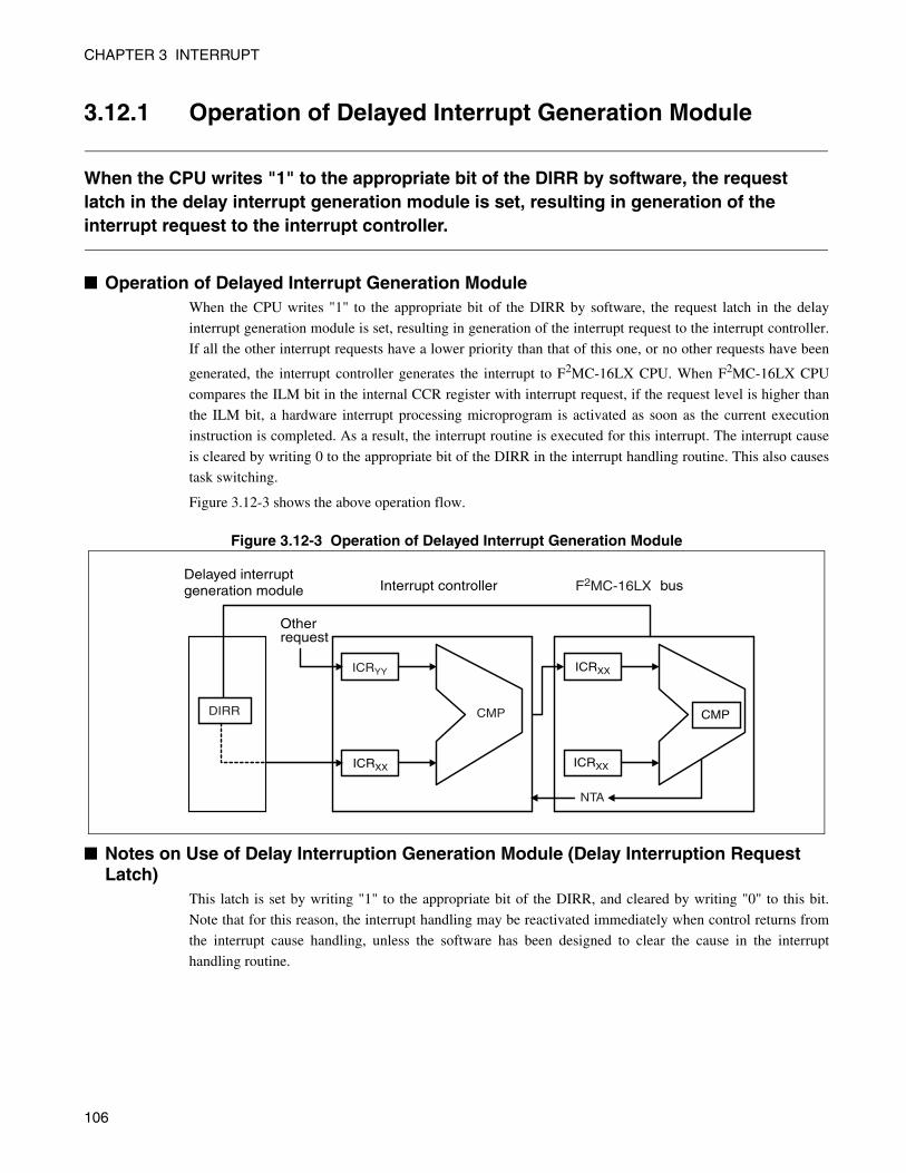
CHAPTER 3 INTERRUPT
3.12.1 Operation of Delayed Interrupt Generation Module
When the CPU writes "1" to the appropriate bit of the DIRR by software, the request latch in the delay interrupt generation module is set, resulting in generation of the interrupt request to the interrupt controller.
Operation of Delayed Interrupt Generation ModuleWhen the CPU writes "1" to the appropriate bit of the DIRR by software, the request latch in the delay
interrupt generation module is set, resulting in generation of the interrupt request to the interrupt controller.
If all the other interrupt requests have a lower priority than that of this one, or no other requests have been
generated, the interrupt controller generates the interrupt to F2MC-16LX CPU. When F2MC-16LX CPU
compares the ILM bit in the internal CCR register with interrupt request, if the request level is higher than
the ILM bit, a hardware interrupt processing microprogram is activated as soon as the current execution
instruction is completed. As a result, the interrupt routine is executed for this interrupt. The interrupt cause
is cleared by writing 0 to the appropriate bit of the DIRR in the interrupt handling routine. This also causes
task switching.
Figure 3.12-3 shows the above operation flow.
Figure 3.12-3 Operation of Delayed Interrupt Generation Module
Notes on Use of Delay Interruption Generation Module (Delay Interruption Request Latch)
This latch is set by writing "1" to the appropriate bit of the DIRR, and cleared by writing "0" to this bit.
Note that for this reason, the interrupt handling may be reactivated immediately when control returns from
the interrupt cause handling, unless the software has been designed to clear the cause in the interrupt
handling routine.
busInterrupt controller
Other request
Delayed interrupt generation module F2MC-16LX
DIRR CMP CMP
ICRYY
ICRXX
ICRXX
ICRXX
NTA
106

CHAPTER 4RESET
This chapter explains reset of the MB90335 series.
4.1 Outline of Reset
4.2 Reset Factors and Oscillation Stabilization Wait Times
4.3 External Reset Pin
4.4 Reset Operation
4.5 Reset Factor Bit
4.6 State of Each Pin at Reset
107

CHAPTER 4 RESET
4.1 Outline of Reset
When the reset cause is generated, the CPU suspends the currently executed process immediately before entering the wait state for release of the reset. After the reset is cleared, processing starts from the address indicated in the reset vector.There are the following four kinds of factors of resets.• Generation power on reset• Watchdog timer overflow• Generation of external reset request from RST terminal• Generation of software reset request
Reset FactorTable 4.1-1 shows the causes of reset.
Power on reset
Power on reset is reset generated at power on. For an evaluation or flash product, the oscillation
stabilization wait time is 218/HCLK (approx. 43.70 ms at an oscillation clock of 6 MHz). For a MASK
product, this wait time is 217/HCLK (approx. 21.85 ms at an oscillation clock of 6 MHz). Reset operation
starts after elapsing the oscillation stabilization wait time.
Watchdog reset
Watchdog reset generates a reset in response to an overflow of the watchdog timer after start of the
watchdog timer. This overflow occurs when a "0" is not written in the watchdog control bit (WTE) of the
watchdog timer control register (WDTC) within the predetermined time. The oscillation stabilization wait
time can be selected using the clock select register (CKSCR).
Table 4.1-1 Reset Factor
Reset Generation factor Machine clock Watchdog timersOscillation
stability waiting
Power on At power onMain clock (MCLK)
Stops Yes
Watchdog timer Watchdog timer overflowMain clock (MCLK)
Stops None
External pin Input "L" level to RST pinMain clock (MCLK)
Stops None
Software
A "0" is written to the RST bit of low-power consumption mode control register (LPMCR)
Main clock (MCLK)
Stops None
Main clock: Oscillation clock frequency divided by 2
108

CHAPTER 4 RESET
External reset
An external reset is generated by inputting the "L" level signal to external reset pin (RST). The input time
of the "L" level signal to the (RST) pin must be continued for 16 machine cycles (16/φ) or more.
The external reset, that is, the RST pin input reset does not produce the oscillation stabilization wait time.
Reference:
Only when a reset request via the RST pin is generated, a reset cause generated in write operation(An example of such write operation is the MOV instruction which is issued during execution of atransfer instruction.) causes a wait state for release of the reset after completion of the instruction.Thus, the write process terminates normally even if a reset signal is input during write operation.
However, if a string instruction such as MOVS is used, transfer of all the data will not be guaranteed.This is because the instruction accepts a reset before the transfer data for the specified countervalue is completed. A reset is accepted also if extension of the bus cycle via the RDY pin continuesfor 16 machine cycles or more during access to the external bus.
Software reset
Software reset causes an internal reset by writing "0" to the internal reset signal generation bit (RST) of the
low-power consumption mode control register (LPMCR). Software reset does not cause the oscillation
stabilization wait time.
Reference:
Clock definition
HCLK: Oscillation clock, which is provided via the high speed oscillation pin.
MCLK: Main clock (HCLK frequency divided by 4)
φ: Machine clock (CPU operation clock)
1/φ: machine cycle (CPU operating clock cycle)
Refer to the "5.1 Outline of Clock" section for details of the machine clocks.
Note:
A reset generated in stop mode produces an 217/HCLK oscillation stabilization wait time (approximately 21.85 ms at the oscillation clock is 6 MHz).
Refer to the "5.4 Clock Mode" section for details of the clock mode.
109

CHAPTER 4 RESET
4.2 Reset Factors and Oscillation Stabilization Wait Times
There are four kinds of reset factors of MB90335 series. The oscillation stabilization wait time varies with the reset cause.
Reset Factors and Oscillation Stabilization Wait TimesTable 4.2-1 shows the relationship between the reset causes and the oscillation stabilization wait time.
Figure 4.2-1 shows the oscillation stabilization wait times for the evaluation/flash and MASK products
during power on reset time.
Table 4.2-1 Reset Factors and Oscillation Stabilization Wait Times
Reset factorOscillation stabilization wait timeEach value in parentheses ( ) represents the period for the oscillation clock at 6 MHz.
Power on resetEvaluation products/flash products: 218/HCLK (about 43.70 ms).
MASK product: 217/HCLK (about 21.85 ms).
Watchdog timer None: However, WS1 and WS0 bit are initialized by "11B".
External reset from RST terminal None: However, WS1 and WS0 bit are initialized by "11B".
Software reset None: However, WS1 and WS0 bit are initialized by "11B".
HCLK: Oscillation clockWS1, WS0: Bits used to select the oscillation stabilization wait time of the clock selection register (CKSCR).
110

CHAPTER 4 RESET
Figure 4.2-1 Oscillation Stabilization Wait Times for the Evaluation/flash and MASK Products during Power on Reset Time
Note:
For ceramic or quartz oscillators, typically the oscillation stabilization wait time of several to sometens of milliseconds is required until the oscillation is stabilized at the natural oscillation. after itbegins. For this reason, set the wait time value meeting the oscillator used.
For details, see "5.5 Oscillation Stabilization Wait Time"
Oscillation Stabilization Waiting Reset StateThe reset operation in response to a reset which occurs during power on reset or in stop mode begins after
passing the oscillation stabilization wait time produced by the timebase timer expires. The reset operation is
performed after the external reset is released.
Evaluation/Flash Products
MASK Products
CPUoperation
CPUoperation
Oscillation Stabilizing Wait Time
Oscillation Stabilizing Wait Time
Oscillation clock
Down-conversionStabilizing Wait Time
217/HCLK217/HCLK
217/HCLK
VCC
VCC
CLK
CLK
HCLK :
111

CHAPTER 4 RESET
4.3 External Reset Pin
The external reset pin (RST pin), dedicated to reset input pin, generates an internal reset in response to input of the "L" level signal. MB90335 series are reset in sync with the CPU operating clock, except for external pin in asynchronous (generated through ports and so on), which change to the reset state.
Block Diagram of External Reset PinFigure 4.3-1 shows the block diagram of the generation of the internal reset.
Figure 4.3-1 Block Diagram of Internal Reset Generation
Note:
To protect the memory from destruction by a reset during write operation, the RST pin input isaccepted with a cycle which does not cause the memory to be destroyed.
Also, the clock is required to initialize the internal circuits. In particular, when using an external clock,the clock must be input during input of the reset.
CPU operation clock(PLL frequency multiplication circuit, divided-by-two of HCLK)
Synchronous circuit
Peripheralfunction
I/O portetc.
Input buffer
Pin
HCLK : Oscillation clock
RST P-ch
N-ch
CPU
112

CHAPTER 4 RESET
4.4 Reset Operation
Once the reset is released, the object from which to read the mode data and reset vector is selected by setting the mode pin, before the mode fetch is performed. This fetch determines the CPU operation mode and the execution activation address succeeding the reset operation. At power on or when recovering from stop mode via a reset, the mode fetch is performed after the oscillation stabilization delay time elapses.
Overview of Reset OperationFigure 4.4-1 shows the reset operation flow.
Figure 4.4-1 Reset Operation Flow
Mode PinThe mode pins (MD2 to MD0) specify the way to fetch the reset vector and mode data. This fetch is
performed according to the reset sequence. See Section "7.2 Mode Pins (MD2 to MD0)" for details of the
mode pins.
Power on resetStop mode
External resetSoftware resetWatchdog timer reset
Oscillation stabilizing waitreset state
Fetch Mode data
Fetch Reset vector
Mode fetch(Reset operation)
During reset
Normal operation(RUN state)
Pin state and function changeof external bus mode relation
Capture the instruction codefrom the address specified by reset vector and execute the instruction
113

CHAPTER 4 RESET
Mode FetchOnce the reset is released, the CPU transfers the reset vector and mode data into the appropriate register in
the CPU core. The reset vector and mode data are assigned to the four bytes of FFFFDCH to FFFFDFH.
When the reset is released, the CPU immediately outputs these addresses to the bus before fetching the
reset vector and mode data. The CPU starts the mode fetch process at the address pointed to by the reset
vector.
Figure 4.4-2 shows how the reset vector and mode data are transferred.
Figure 4.4-2 Reset Vector and Mode Data Transfers
Reference:
The object from which to read the reset vector and mode data (either internal ROM or externalmemory) can be specified using the mode pins. It is recommended that the internal vector mode bespecified using the mode pins in single chip mode or internal ROM external bus mode. This isbecause specifying the external vector mode with the mode pins causes an attempt to read the resetvector and mode data from the external memory, instead of the internal memory.
Mode data (address: FFFFDFH)
The contents of the mode register can be modified only by reset operation. The mode register settings will
take effect after reset operation. Refer to the "7.3 Mode Data" section for details of the mode data.
Reset vector (address "FFFFDCH to FFFFDEH")
Write the execution start address after the completion of the reset operation. Execution begins from the
address of this content.
Memory space
Mode data
Reset vector bit 23 to 16
Reset vector bit 15 to 8
Reset vector bit 7 to 0
Moderegister
Reset sequence
Micro ROM
PCB
PC
FFFFDFH
FFFFDEH
FFFFDDH
FFFFDCH
F2MC-16LX CPU core
114
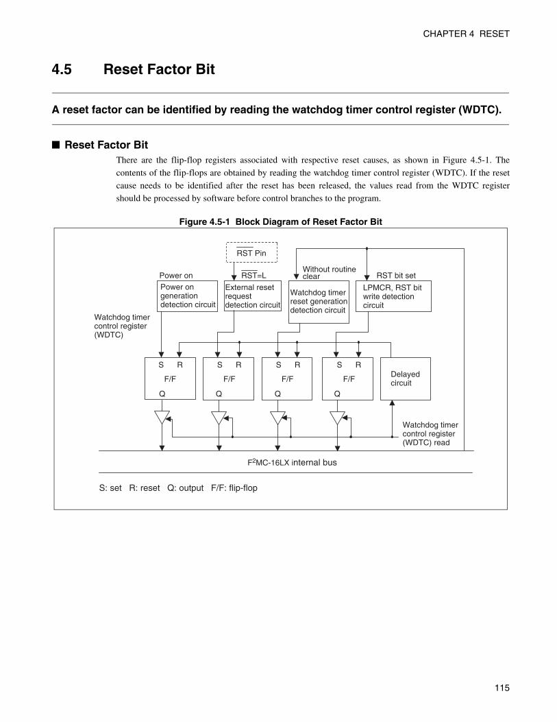
CHAPTER 4 RESET
4.5 Reset Factor Bit
A reset factor can be identified by reading the watchdog timer control register (WDTC).
Reset Factor BitThere are the flip-flop registers associated with respective reset causes, as shown in Figure 4.5-1. The
contents of the flip-flops are obtained by reading the watchdog timer control register (WDTC). If the reset
cause needs to be identified after the reset has been released, the values read from the WDTC register
should be processed by software before control branches to the program.
Figure 4.5-1 Block Diagram of Reset Factor Bit
RST Pin
Power on
Power on generationdetection circuit
External resetrequest detection circuit
RST bit set
LPMCR, RST bit write detection circuit
Watchdog timercontrol register (WDTC)
Watchdog timercontrol register (WDTC) read
Watchdog timerreset generationdetection circuit
Delayedcircuit
F2MC-16LX internal bus
S: set R: reset Q: output F/F: flip-flop
Without routine clear
S R S R S R S R
F/F F/F F/F F/F
Q QQQ
RST=L
115

CHAPTER 4 RESET
Correspondence of Reset Factor Bit and Reset FactorFigure 4.5-2 shows the configuration of the reset cause bits of the watchdog timer control register (WDTC).
Contents of reset cause bits and associated reset causes are shown in the Table 4.5-1.
For details, see the "10.2 Watchdog Timer Control Register (WDTC)" section.
Figure 4.5-2 Configuration of Reset Factor Bits (Watchdog Timer Control Register)
Notes on Reset Factor Bit
At two or more reset factors
If more than one reset cause is generated, the corresponding each reset cause bits of the WDTC register will
be set to "1". For example, if an external reset request via the RST pin and an overflow are generated
simultaneously, ERST and WRST of reset cause bits are set to "1".
At power on reset
When a power on reset is generated, the PONR of reset cause bit is set to "1" and all the other reset cause
bits are made undefined. For this reason, the software must be designed so that all the reset cause bits other
than PONR will be ignored if PONR is "1".
Clearing of reset factor bit
Each of the reset cause bits is cleared only when the values are read from the WDTC register. Once a reset
cause is generated, the bit corresponding to it is not cleared even when the reset is generated (a setting of
"1" is retained).
Note:
If power is turned on when a power on reset has not been generated, the WDTC register values maybe unprotected.
Table 4.5-1 Correspondence of Reset Factor Bit and Reset Factor
Reset Factor PONR WRST ERST SRST
Generating power-on reset 1 X X X
Generating watchdog timer overflow * 1 * *
Generating External reset request from RST terminal * * 1 *
Generation of software reset request * * * 1
* : Preserving the previous stateX : Indeterminate
Initial value
Bit
R: Read only W: Write only X: Indeterminate
15 - 8
0000A8H
7 6 5 4 3 2 1 0
(TBTC) PONR Reserved WRST ERST SRST WTE WT1 WT0
X X X X X 1 1 1R - R R R W W W R/W
Watchdog Timer Control Register (WDTC)
116
CHAPTER 4 RESET
4.6 State of Each Pin at Reset
This section explains the state of each pin at reset.
Pin Status during ResetThe state of each pin during reset is determined by the settings of the mode pins (MD2 to MD0).
When internal vector mode has been set: (MD2 to MD0="011B")
All I/O, or resource, pins are placed at high impedance. The internal ROM is defined as the object form
which to read the mode data.
See the "6.7 State of the Pin during Standby Mode, and Reset" section for details of the state of each pin
during reset."
State of Pins after Mode Data ReadThe pin state succeeding read of the mode data is determined by the mode data (M1, M0).
When single chip is selected a mode (M1,M0="00B")
All I/O, or resource, pins are placed at high impedance. The internal ROM is defined as the object form
which to read the mode data.
Note:
For any pin to which place at high impedance when a reset cause is generated, give considerationso that the equipment connected to the pin will not malfunction.
117

CHAPTER 4 RESET
118

CHAPTER 5CLOCK
This chapter explains the clock of the MB90335 series.
5.1 Outline of Clock
5.2 Block Diagram of Clock Generation Section
5.3 Clock Select Register (CKSCR)
5.4 Clock Mode
5.5 Oscillation Stabilization Wait Time
5.6 Connection of Oscillator and External Clock
119

CHAPTER 5 CLOCK
5.1 Outline of Clock
The clock generation section controls operation of the internal clock which is the operation clock for the CPU and peripheral functions. The following are four kinds of the clock.• Machine clock: Internal clock.• Machine cycle: 1 cycle of machine clock.• Oscillation clock: Clock provided via a high-speed oscillation pin.• PLL clock: Clock generated by internal PLL oscillation.
Overview of ClockThe clock generation section, containing an oscillator circuit, can generate the oscillation clock by being
connected with an external oscillator. Clock generated externally can be input and used as the oscillation
clock. The generator, also containing a PLL clock frequency multiplication circuit, can generate three
frequency multiplication clocks of the oscillation clock. The clock generation section controls the
oscillation stabilization wait time, controls the PLL clock multiplication and controls the internal clock
operation by clock switching with the clock selector.
Oscillation clock (HCLK)
This clock is generated by connecting an oscillator or inputting an external clock to the high-speed
oscillation pins.
Main clock (MCLK)
It is an oscillation clock frequency divided by 2 and an input clock to the timebase timer and clock selector.
PLL clock (PCLK)
An oscillation clock which is obtained by frequency multiplication through the internal PLL clock
frequency multiplication circuit (PLL oscillator circuit). Three kinds of clocks can be selected.
Machine clock (φ)
Operation clock for CPU and peripheral functions. One cycle of this clock is used as machine cycle (1/φ).
A desired clock can be selected from among the main clock, that is, an oscillation clock frequency divided
by 2 and the three frequency multiplication clocks.
Notes:
• As for the oscillation clock, 1 MHz to 7 MHz can oscillate. The maximum operating frequency is24 MHz for the CPU and peripheral functions. When multiplier exceeding the maximum operatingfrequency is specified, the device does not operate correctly. If the source oscillation at afrequency of 6 MHz, only 4-time frequency multiplication can be specified.
• To use the USB Mini-HOST or USB function, the PLL clock mode must have been set.
120

CHAPTER 5 CLOCK
Clock Supply MapMachine clocks generated by the clock generation section are supplied as operating clocks of the CPU and
peripheral function. For this reason, operation of the peripheral functions is influenced by switching clock
mode between the main and PLL clock or switching the PLL clock frequency multiplication rate. The
frequency divided output from the timebase timer is provided to some peripheral functions, thereby
enabling each periphery to select its operating clock. Figure 5.1-1 contains the map showing how the clocks
are provided.
Figure 5.1-1 Clock Supply Map
Clock generation unit
Systemclock
generationcircuit
Pin
Pin
Pin
Pin
Pin
Pin
Pin
Pin
Pin
Pin
Pin
Pin
Pin
Pin
Pin
Pin
Pin
Pin
Pin
Pin
Pin
Timebase timer
Clock selector
PLL frequency multiplication circuit
2 division
: Oscillation clock: Main clock: PLL clock: Machine clock
Peripheral function
Watchdog timer
16-bit PPG timer0/1/2/3/4/5
16-bit reload timer 0
16-bit PWC timer
8-bit expanded serial I/O
External interrupt
USB function
Oscillation stabilization wait time
PPG0 to PPG3
PWC
SCK
SIN
SCK0, SCK1
SOT
SIN0, SIN1UART0/1/2/3
SOT0, SOT1
TIN0
TOT0
INT0 to INT7
DVP
DVM
HCON
UTEST
HVP
HVM
SCL0
SDA0
USB Mini-HOST
I2C interface
3
4
X0
X1
1 2 4
φ
CPUµ DMAC
HCLK MCLK
PCLK
HCLKMCLKPCLKφ
121

CHAPTER 5 CLOCK
5.2 Block Diagram of Clock Generation Section
The clock generation section consists of the following five blocks:• System clock generation circuit• PLL multiplying circuit• Clock selector• Clock select register (CKSCR) • Oscillation stabilization wait time selector
Block Diagram of Clock Generation SectionFigure 5.2-1 shows the block diagram of the clock generation section.
Figure 5.2-1 contains the standby control and timebase timer circuits.
Figure 5.2-1 Block Diagram of Clock Generation Section
Low power consumption mode control register (LPMCR)
CPU intermittent operation sector
Standby control circuit
Reset (Cancellation)
Interrupt (Cancellation)
Clock generation unit
Machineclock
Pin high impedance
control circuit
Internal resetgeneration
circuit
CPU clockcontrol circuit
Peripheral clock
control circuit
Stop signal
Main clock oscillation stabilization wait cancellation
Stop, Sleep signal
CPU clock
Internal reset
Pin highimpedancecontrol
Intermittent cycle selection
Oscillation stable wait cancellation
Oscillation stable wait time selector
Operation clock selector
PLL frequency multiplication circuit
System clockgeneration circuit
Clock selection register (CKSCR)
2-division
512-division
2-division
2-division
2-division
Timebase timerto Watchdog timer
Oscillation clock(HCLK)
X0
2
X1
PinRST
Pin
Pin
STP RSTSLP CG1 CG0 ReservedSPL TMD
RESERVED WS0MCM MCS CS1 CS0WS1
2
2
Mainclock
4-division
2-division
2-division
4-division
RESERVED
122

CHAPTER 5 CLOCK
System clock generation circuit
Generates an oscillation clock (HCLK) using the oscillator connected to the high-speed oscillation pin. It is
also possible to input an external clock.
PLL multiplying circuit
The oscillation clock is multiplied by PLL oscillation and supplied to the CPU clock selector.
Clock selector
From the main clock, and the three PLL clocks, this selects the clock to be supplied to the CPU and
periphery clock control circuits.
Clock select register (CKSCR)
Switches between the oscillation and PLL clocks, selects the oscillation stabilization wait time, and selects
the PLL clock multiplier.
Oscillation stabilization wait time selector
A circuit which selects the oscillation stabilization wait time for the oscillation clock succeeding release of
the stop mode or a watchdog reset. Four timebase timer outputs are selected.
123
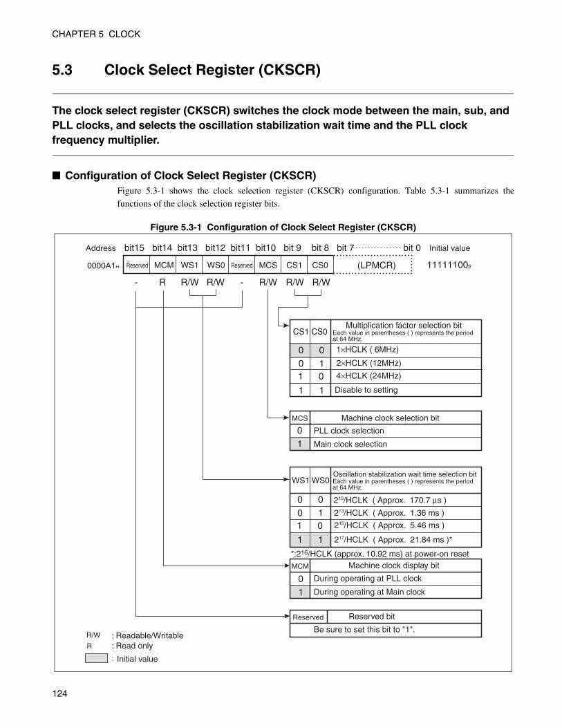
CHAPTER 5 CLOCK
5.3 Clock Select Register (CKSCR)
The clock select register (CKSCR) switches the clock mode between the main, sub, and PLL clocks, and selects the oscillation stabilization wait time and the PLL clock frequency multiplier.
Configuration of Clock Select Register (CKSCR)Figure 5.3-1 shows the clock selection register (CKSCR) configuration. Table 5.3-1 summarizes the
functions of the clock selection register bits.
Figure 5.3-1 Configuration of Clock Select Register (CKSCR)
Initial valueAddress
Multiplication factor selection bitEach value in parentheses ( ) represents the period at 64 MHz.
Oscillation stabilization wait time selection bitEach value in parentheses ( ) represents the period at 64 MHz.
Disable to setting
Machine clock selection bit
PLL clock selection
Main clock selection
Machine clock display bit
During operating at PLL clock
During operating at Main clock
: Readable/Writable: Read only
Initial value
*:216/HCLK (approx. 10.92 ms) at power-on reset
0000A1H Reserved MCM WS1 WS0 Reserved MCS CS1 CS0
bit15 bit14 bit13 bit12 bit11 bit10 bit 9 bit 8 bit 7 bit 0
11111100B(LPMCR)
- R R/W R/W - R/W R/W R/W
CS1 CS0
1 0
1 1
0 10 0 1×HCLK ( 6MHz)
2×HCLK (12MHz)
4×HCLK (24MHz)
MCS
01
WS1 WS0
1 0
1 1
0 10 0
213/HCLK ( Approx. 1.36 ms )
215/HCLK ( Approx. 5.46 ms )
217/HCLK ( Approx. 21.84 ms )*
MCM
01
R/W
R
Reserved bit
Be sure to set this bit to "1".
Reserved
124

CHAPTER 5 CLOCK
Note:
The machine clock selection bit (MCS) is initialized by reset to main clock selection.
Table 5.3-1 Functions of Clock Select Register (CKSCR) Bits
Bit name Functions
bit15Reserved: Reserved bit
The bit always returns "1" when read.
bit14MCM: PLL Clock display bit
• Bit indicating the main or PLL clock, whichever selected as the machine clock.• A "0" in this bit indicates that the PLL clock has been selected. A "1" in the bit indicates that the
main or sub clock has been selected.• If the PLL clock selection bit (MCS) = 0 and MCM = 1, now is the PLL clock oscillation
stabilization wait time.• Writing this bit has no effect on operation.
bit13bit12
WS1, WS0: Oscillation stabilization wait time selection bits
• These bits are used to select an oscillation stabilization wait time required for the oscillationclock when the stop mode is canceled.
• Initialized to "11B" by every reset cause.Note:The oscillation stabilization wait time must be set to a suitable value for the oscillator to use. See"4.2 Reset Factors and Oscillation Stabilization Wait Times". Please set the setting of "00B" onlyat the main clock mode.Reference:
The oscillation stabilization wait time for PLL clock is fixed to 214/HCLK.
bit11Reserved: Reserved bit
Be sure to set this bit to "1".
bit10MCS: PLL clock selection bit
• Bit for selecting main or PLL clock as the machine clock.• A "0" in this bit selects the PLL clock. A "1" in the bit selects the main clock.• If "0" is written to this bit when it is "1", the PLL clock oscillation stabilization wait time is
produced, thereby clearing the timebase timer automatically. Also, the interrupt request flag bit(TBOF) of the timebase timer control register (TBTC) is cleared.
• The PLL clock oscillation stabilization wait time is fixed to 214/HCLK. (If the oscillation clockis 6 MHz, the oscillation stabilization wait time will be approximately 2.73 ms.)
• If the main clock is selected, the operating clock frequency will be the oscillation clockfrequency-divided by 2. (If the oscillation clock is 6 MHz, the operating clock will be 3 MHz.)
• Initialized to "1" by every reset cause.Note:To write "0" if when MCS bit is "1", make sure that the timebase timer interrupt have beenmasked using the TBTC register interrupt request enable bit (TBIE) or interrupt level maskregister (ILM).
bit9bit8
CS1, CS0: Multiplier selection bits
• Bit for selecting the multiply factor for PLL clock.• The multiplier can be selected from among three options.• Initialized to "00B" by every reset cause.Note: When the MCS or MCM is "0", writing to these bits is not allowed. Rewrite the CS1 and CS0 bitsafter setting the MCS bit to "1" once. "11B" is a set interdiction.
HCLK: Oscillation clock
125

CHAPTER 5 CLOCK
5.4 Clock Mode
The clock modes are the main clock mode and PLL clock mode.
Main Clock Mode, PLL Clock Mode
Main clock mode
The main clock mode stops the PLL clock by using an oscillation clock frequency divided by 2 as theoperating clock of the CPU and peripheral resources.
PLL clock mode
The PLL clock mode uses the PLL clock as operation clock for the CPU and peripheral functions. The PLLclock frequency multiplier factor can be selected using the clock selection register (CKSCR).
Note:
To use the USB Mini-HOST or USB function, the PLL clock mode must have been set.
Transition of Clock ModeWriting the PLL clock selection bit (MCS) of the CKSCR changes the clock mode to main or PLL.
Transition from main clock mode to PLL clock mode
If the CKSCR of MCS bit is rewritten from "1" to "0" while in the main clock mode, the mode will change
from main to PLL after the PLL clock oscillation stabilization wait time (214/HCLK).
Transition from PLL clock mode to main clock mode
If the CKSCR of MCS bit is rewritten from "0" to "1" while in the PLL clock mode, the mode will changefrom PLL to main when the PLL and main clock edges will match (after 1 to 8 PLL clocks).
Note:
Even if the PLL clock selection (MCS) bit of the CKSCR is rewritten, the machine clock is notswitched immediately. If a resource which depends on the machine clock needs to be operated, referthe PLL clock indicator bit (MCM) of the CKSCR to check that the machine clock has been switched,before beginning the operation.
If the clock mode is switched, the mode must not be switched to another clock mode or the low-power consumption mode until completion of the switching. Completion of the switching can bechecked by referring the MCM bit of the CKSCR.
Selection of PLL Clock Multiplication RateOne of the three PLL clock frequency multiplier from 1 to 4 times can be selected by writing "00B" to
"10B" to the CS1 and CS0 bits of the CKSCR. "11B" is a set interdiction.
126

CHAPTER 5 CLOCK
Machine ClockThe PLL clock and main clock output from the PLL multiplying circuit are used as machine clocks. These
machine are clocks supplied to the CPU or peripheral function. One of the main and PLL modes can be
selected by writing the CKSCR of MCS bit.
Figure 5.4-1 shows the transition chart of the machine clock selection.
Figure 5.4-1 State Transition Diagram of Machine Clock Selection
Note:
The initial value for machine clock is the main clock (MCS = 1).
MainMCS = 1MCM = 1
CS1,CSO = xx
Main → PLLxMCS = 0MCM = 1
CS1,CSO = xx
PLL1 → MainMCS = 1MCM = 0
CS1,CSO = 00
PLL2 → MainMCS = 1MCM = 0
CS1,CSO = 01
PLL4 → MainMCS = 1MCM = 0
CS1,CSO = 10
PLL1 multiplication
MCS = 0MCM = 0
CS1,CSO = 00
PLL2 multiplication
MCS = 0MCM = 0
CS1,CSO = 01
PLL4 multiplication
MCS = 0MCM = 0
CS1,CSO = 10
(1)
(6)(2)
(3)(4)
(6)
(6)
(6)
(6)(5)
(5)
(5)
MCS bit "0" writePLL clock oscillation stabilization wait end & CS1, CS0=00PLL clock oscillation stabilization wait end & CS1, CS0=01PLL clock oscillation stabilization wait end & CS1, CS0=10MCS bit "1" write (within Watchdog reset)Synchronous timing of PLL clock and Main clock
MCSMCMCS1, CS0
: PLL clock selection bit of Clock selection register (CKSCR): PLL clock display bit of Clock selection register (CKSCR): Multiplication factor selection bit of Clock selection register (CKSCR)
(1)(2)(3)(4)(5)(6)
127

CHAPTER 5 CLOCK
5.5 Oscillation Stabilization Wait Time
When power is turned on, the stop mode is quit, the oscillation stabilization wait time is required after the oscillation begins. This is because the oscillation of the oscillation clock remains in stopped state. Also when the clock mode changes from main to PLL, the oscillation stabilization wait time is required after the PLL oscillation begins.
Oscillation Stabilization Wait TimeIn general, ceramic and crystal oscillators require several milliseconds to some tens of milliseconds until
the they provide stable oscillation at their natural frequency (oscillation frequency). Accordingly, CPU
operation is disabled immediately after the oscillation starts and the clock supply to the CPU is enabled
until the oscillation stabilization wait time has elapsed. This gives the oscillation time to stabilize. It is
necessary to select a oscillation stabilization wait time appropriate to an oscillator to be used because the
oscillation stabilization time depends on the type of oscillator (crystal, ceramic, etc.). The oscillation
stabilization wait time can be selected by setting in the clock selection register (CKSCR).
When changing the clock mode from main to PLL, the CPU operates with the main clock during the PLL
oscillation stabilizing wait time before the mode actually changes to PLL.
Figure 5.5-1 shows the operation immediately after starting the oscillation.
Figure 5.5-1 Operation Immediately after the Start of Oscillation
Oscillation stabilization
Oscillation stabilization wait time
Oscillation time of oscillator
Oscillation start
Starting normal operation or switching to PLL clock
X1
128

CHAPTER 5 CLOCK
5.6 Connection of Oscillator and External Clock
MB90335 series, containing a system clock generator circuit, generates the clock with the oscillator connected externally. It is also possible to input an externally generated clock.
Connection of Oscillator and External Clock
Example of connection of crystal oscillator or ceramic oscillator
Connect the crystal or ceramic oscillator as shown in Figure 5.6-1.
Figure 5.6-1 Example of Connection of Crystal Oscillator or Ceramic Oscillator
Example of connection of external clock
As shown in Figure 5.6-2, connect the external clock to the X0 pin and open the X1 pin.
Figure 5.6-2 Example of Connection of External Clock
MB90335 series
X0 X1
Open
MB90335 series
X0 X1
129

CHAPTER 5 CLOCK
130

CHAPTER 6LOW-POWER
CONSUMPTION MODE
This chapter describes the low-power consumption mode of the MB90335 series.
6.1 Outline of Low-Power Consumption Mode
6.2 Block Diagram of Low-power Consumption Control Circuit
6.3 Low-power Consumption Mode Control Register (LPMCR)
6.4 CPU Intermittent Operation Mode
6.5 Standby Mode
6.6 State Transition Diagram
6.7 State of the Pin during Standby Mode, and Reset
6.8 Precautions when Using Low-power Consumption Mode
131

CHAPTER 6 LOW-POWER CONSUMPTION MODE
6.1 Outline of Low-Power Consumption Mode
The MB90335 series have the following CPU operation modes by selecting the operation clock and operating the control of the clock.• Clock mode
(PLL clock mode and main clock mode)• CPU Intermittent operation mode
(PLL clock intermittent operation mode and main clock intermittent operation mode) • Standby mode
(sleep mode, timebase timer mode, and stop mode)
CPU Operation Modes and Current ConsumptionFigure 6.1-1 shows the relationships between the CPU operation modes and current consumption.
Figure 6.1-1 CPU Operation Modes and Current Consumption
Current consumption
Several mA
Several dozen mA
Several µA
CPU Operation mode
PLL clock mode Clock multiplied by four
Clock multiplied by two
Clock multiplied by one
PLL clock intermittent operation mode
Clock multiplied by four
Clock multiplied by two
Clock multiplied by one
Main clock mode (1/2 HCLK)
Main clock intermittent operation mode
Standby mode Sleep mode
Timebase timer mode
Stop mode
Low-power consumption mode
Note: This diagram shows an image of each mode, so its values may differ from actual current consumption.
132
CHAPTER 6 LOW-POWER CONSUMPTION MODE
Clock Mode
PLL clock mode
In PLL clock mode, the CPU and peripheral function operate on a PLL multiplying clock of oscillation
clock (HCLK).
Note:
When using USB Mini-HOST and the USB function, you need to set to the PLL clock mode.
Main clock mode
In main clock mode, the CPU and peripheral function operate on a clock with 2-frequency division of
oscillation clock (HCLK). In this mode, the PLL multiplying circuit stops.
Reference:
For the clock mode, see section "5.4 Clock Mode".
CPU Intermittent Operation ModeThe CPU intermittent mode operates the CPU intermittently and lowers the power consumption while
supplying the high-speed clock to the peripheral functions. The CPU intermittent operation mode is a mode
for supplying intermittent clock only to the CPU when it makes access to the registers, internal memory,
peripheral functions, or external devices.
Standby ModeStandby mode reduces the power consumption by the low-power consumption control circuit which stops
clock supply to the CPU (sleep mode), stops clock supply to the CPU and peripheral functions (timebase
timer mode), or stops the oscillation clock (stop mode).
PLL sleep mode
The PLL sleep mode terminates the CPU operation clock in the PLL clock mode and operates components
except for CPU under the PLL clock.
Main sleep mode
The main sleep mode terminates the CPU operation clock in the main clock mode and operates components
except for the CPU under the main clock.
Timebase timer mode
The timebase timer mode terminates all the operations other than the oscillation clock, the timebase timer,
and the clock timer, terminating all the functions other than the timebase timer and the watch timer.
133

CHAPTER 6 LOW-POWER CONSUMPTION MODE
Stop mode
Stop mode is mode for stopping original oscillation and all functions are stopped.
Note:
In the stop mode, data is kept at the lowest power consumption since the oscillation clock isterminated.
When you change the clock mode, be sure not to shift to other clock modes or the low-powerconsumption mode until you complete the clock mode change. Completion of the switching can bechecked by referring the MCM bit of the CKSCR.
The transition to the standby mode is a prohibited at USB transferring.
134

CHAPTER 6 LOW-POWER CONSUMPTION MODE
6.2 Block Diagram of Low-power Consumption Control Circuit
The low-power consumption control circuit is composed of the following seven blocks.• CPU intermittent operation selector• Standby controller circuit• CPU clock controller circuit• Peripheral clock controller circuit• Pin high-impedance controller circuit• Internal reset generator circuit• Low-power consumption mode control register (LPMCR)
Block Diagram of Low-power Consumption Control CircuitFigure 6.2-1 shows the block diagram of the low-power consumption control circuit.
Figure 6.2-1 Block Diagram of Low-power Consumption Control CircuitLow power consumption mode control register (LPMCR)
CPU intermittent operation sector
Standby control circuit
Reset (Cancellation)
Interrupt (Cancellation)
Clock generation unit
Machineclock
Pin high impedance
control circuit
Internal resetgeneration
circuit
CPU clockcontrol circuit
Peripheral clock
control circuit
Stop signal
Main clock oscillation stabilization wait cancellation
Stop, Sleep signal
CPU clock
Internal reset
Pin highimpedancecontrol
Intermittent cycle selection
Oscillation stable wait cancellation
Oscillation stable wait time selector
Operation clock selector
PLL frequency multiplication circuit
System clockgeneration circuit
Clock selection register (CKSCR)
2-division
512-division
2-division
2-division
2-division
Timebase timerto Watchdog timer
Oscillation clock(HCLK)
X0
2
X1
PinRST
Pin
Pin
STP RSTSLP CG1 CG0 ReservedSPL TMD
RESERVED WS0MCM MCS CS1 CS0WS1
2
2
Mainclock
4-division
2-division
2-division
4-division
RESERVED
135

CHAPTER 6 LOW-POWER CONSUMPTION MODE
CPU intermittent operation selector
The CPU intermittent operation sector selects the number of the suspended clocks in the CPU intermittent
operation mode.
Standby controller circuit
The standby controller circuit controls the CPU clock control circuit and the peripheral clock control
circuit, and then performs the transition to the low-power consumption mode or cancellation.
CPU clock controller circuit
The CPU clock controller circuit controls the clock supplied to CPU.
Peripheral clock controller circuit
The peripheral clock controller circuit controls the clock supplied to the peripheral functions.
Pin high-impedance controller circuit
The pin high-impedance controller circuit makes the external pin to the high-impedance while the mode is
in the timebase timer mode and the stop mode. For the pin to which pull-up option is selected, you need to
cut the pull-up resistance during the stop mode.
Internal reset generator circuit
This circuit generates internal reset signals.
Low-power consumption mode control register (LPMCR)
The low-power consumption mode control register (LPMCR) shifts to/cancels the standby mode or sets the
CPU intermittent operation function.
136

CHAPTER 6 LOW-POWER CONSUMPTION MODE
6.3 Low-power Consumption Mode Control Register (LPMCR)
The low-power consumption mode control register (LPMCR) performs transition to/cancellation of the low-power consumption mode or sets the number of the CPU clock suspend cycles in the CPU intermittent operation mode.
Low-power Consumption Mode Control Register (LPMCR)Figure 6.3-1 shows the configuration of the low-power consumption mode control register (LPMCR).
Figure 6.3-1 Configuration of Low-power Consumption Mode Control Register (LPMCR)
Initial valueAddress
RESV
RESV Reserved
Count bit for CPU clock temporary halt cycle
Timebase timer mode bit
Switches to the timebase timer mode
No change, no effect on operation
Internal reset signal generation bit
Watch and pin state setting bit(for timebase timer mode and stop mode)
Sleep mode bit
: Read/write: Write-only: Initial value
Generates an internal reset signal of three machine cycles
No change, no effect on operation
Previous pin state retained
High impedance
No change, no effect on operation
Switches to sleep mode
Stop mode bit
No change, no effect on operation
Switches to stop mode
0 cycles (CPU clock = Resource clock)
8 cycles (CPU clock: Resource clock = 1:3 to 4 approx.)
16 cycles (CPU clock: Resource clock = 1:5 to 6 approx.)
32 cycles (CPU clock: Resource clock = 1:9 to 10 approx.)
Always write "0" to this bit
bit15 bit7 bit6 bit5 bit4 bit3 bit2 bit1 bit0
STP SLP SPL RST TMD CG1 CG0
W W R/W W W R/W R/W R/W
(CKSCR)0000A0H 00011000B
R/WW
0
0 0
1 1
0 11 0
0
1
0
1
0
1
0
1
0
1
CG1 CG0
TMD
RST
STP
SLP
SPL
137

CHAPTER 6 LOW-POWER CONSUMPTION MODE
Table 6.3-1 Function Description of Each Bit of Low-power Consumption Mode Control Register (LPMCR)
Bit name Functions
bit7 STP: Stop mode bit
• This bit indicates the transition to the stop mode.• Writing "1" to this bit changes the stop mode.• Writing "0" to this bit has no influence on operation.• Cleared to "0" by generation of a reset or interrupt request.• The bit always returns "0" when read.
bit6 SLP: Sleep mode bit
• This bit indicates the transition to the sleep mode.• Writing "1" to this bit changes the sleep mode.
Writing "0" to this bit has no influence on operation.• Cleared to "0" by generation of a reset or interrupt request.• The bit always returns "0" when read.
bit5
SPL: Pin state specification bit(At the stop mode of the timebase timer)
• Valid only while in the timebase timer, or stop mode.• A "0" in this bit causes the clock to remain at the level of the external pin.• An external terminal is made high impedance in case of "1".• The bit is initialized to "0" at a reset.
bit4 RST: Internal reset signal generation bit
• Writing "0" to this generator generates the internal reset signal three machine cycle.• Writing "1" to this bit has no influence on operation.• The bit always returns "1" when read.
bit3 TMD: Timebase timer mode bit
• This bit indicates the transition to the timebase timer mode.• Writing "0" to this bit while in main or PLL clock mode changes the timebase timer
mode.• Initialized to "1" by generation of a reset or interrupt request.• The bit always returns "1" when read.
bit2bit1
CG1,CG0: Temporary CPU clock stop cycle count selection bits
• Bit used for setting the number of suspension cycles of the CPU clock for CPU intermittent operation function.
• Stops the CPU clock supply for the specified number of cycles each time the instruction is executed once.
• Selectable from four types of clocks counts.• The bit is initialized to "00B" at a reset.
bit0Reserved:Reserved bit
• Be sure to set this bit to "0".
138

CHAPTER 6 LOW-POWER CONSUMPTION MODE
Access to Low-power Consumption Mode Control RegisterTransition to the low-power consumption modes (stop mode, sleep mode, and timebase timer mode) by
writing to the low-power consumption mode control register is made, in this case, be sure to use the
instructions in Table 6.3-2.
The low-power consumption mode transition instruction in Table 6.3-2 must always be followed by an arrayof instructions highlighted by a line below.
MOV LPMCR, #H'XX ; the low-power consumption mode transition instruction in Table 6.3-2
MOV A,#H'10 ; any instruction
The devices does not guarantee its operation after returning from the low-power consumption mode if youplace an array of instructions other than the one enclosed in the dotted line. To access the low-powerconsumption mode control register (LPMCR) with C language, refer to "Notes on Accessing the Low-Power Consumption Mode Control Register (LPMCR) to Enter the Standby Mode" in the section "6.8Precautions when Using Low-power Consumption Mode".
To write word length data into the low-power consumption mode control register (LPMCR), use even
addresses. Transition to the low-power consumption mode is made by writing at odd addresses may cause
an erroneous operations.
When you control other functions than the functions listed in Figure 6.3-1, you may use any instruction.
Priority Level of STP, SLP, and TMD BitWhen the stop mode, sleep mode, and timebase timer mode requests are performed at the same time,
requests are processed according to the following order.
Stop mode request > timebase timer mode request > sleep mode request
NOP
NOP
JMP $+3 ; jump to next instruction
Table 6.3-2 List of Instructions Used for Transition to Low-power Consumption Mode
MOV io,#imm8 MOV dir,#imm8 MOV eam,#imm8 MOV eam,Ri MOV io,A MOV dir,A MOV addr16,A MOV eam,A MOV @RLi+disp8,AMOVW io,#imm16 MOVW dir,#imm16 MOVW eam,#imm16 MOVW eam,RWi MOVW io,A MOVW dir,A MOVW addr16,A MOVW eam,A MOVW @RLi+disp8,ASETB io:bp SETB dir:bp SETB addr16:bpCLRB io:bp CLRB dir:bp CLRB addr16:bp
139

CHAPTER 6 LOW-POWER CONSUMPTION MODE
6.4 CPU Intermittent Operation Mode
The CPU intermittent operation mode is a mode for reducing the power consumption by intermittently operating the CPU while operating the external bus and peripheral functions at high speed.
CPU Intermittent Operation ModeThe CPU intermittent operation mode is a mode for stopping the clock supplied to the CPU for a
predetermined period of time for each instruction execution to delay the internal bus cycle start when
accessing the registers, internal memory (ROM, RAM), I/O, peripheral functions, or external bus. If the
CPU operation speed is decreased while supplying a high-speed peripheral clock to the peripheral
functions, processing at low-power consumption becomes available.
• Selection of the number of the suspend cycles of the clock supplied to CPU is made in the CPU clock
suspend cycle number selection bit (CG1 and CG0) of the low-power consumption mode control
register (LPMCR).
• The external bus operation itself uses the same clock as the peripheral functions.
• The instruction execution time in CPU intermittent operation mode can be calculated by adding to the
ordinary execution time the compensation value obtained by multiplying the instruction execution count
for accessing the registers, internal memory, internal peripheral function, and external bus by the
number of suspension cycles. Figure 6.4-1 shows the operation clock for CPU intermittent operation
mode.
Figure 6.4-1 Clock for the CPU Intermittent Operation Mode
Peripheral clock
CPU clock
Suspended cycle
Internal bus activation
1 instruction execution cycle
140
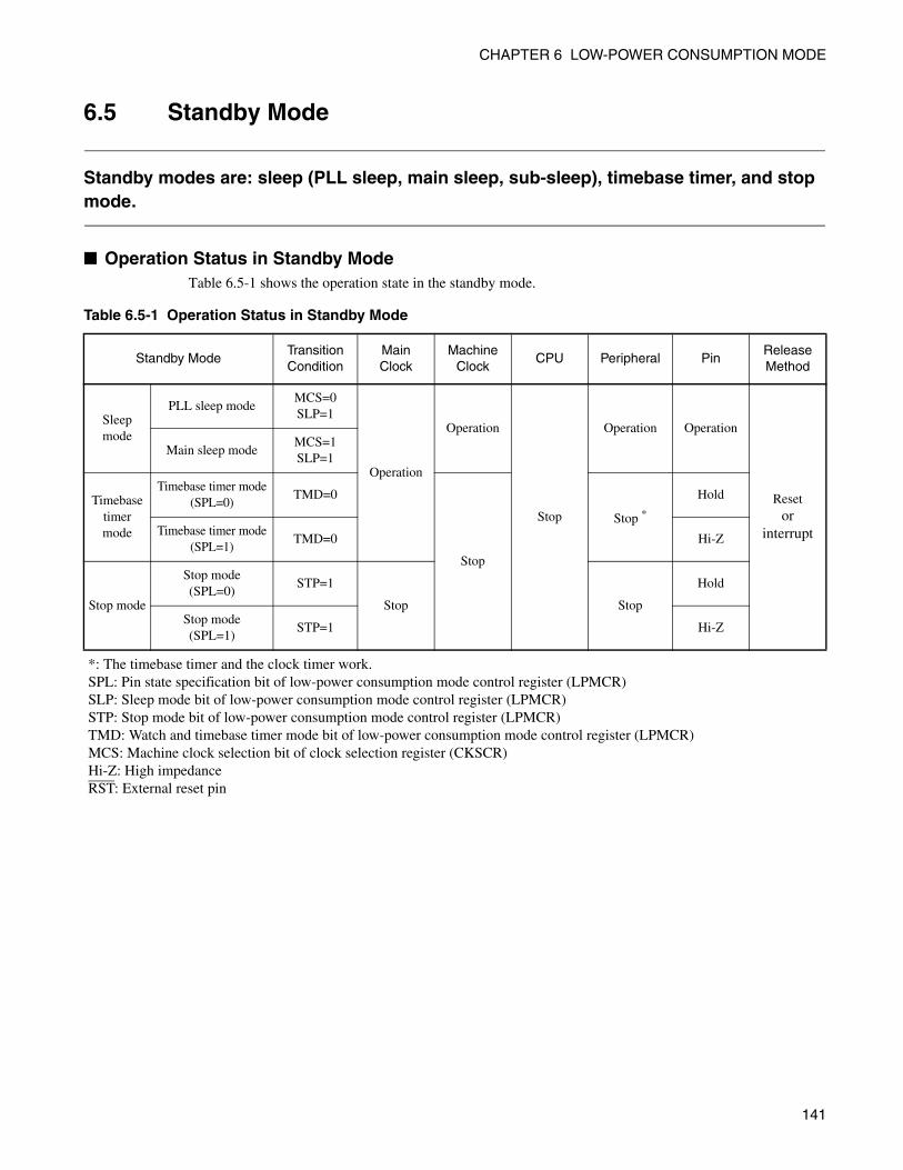
CHAPTER 6 LOW-POWER CONSUMPTION MODE
6.5 Standby Mode
Standby modes are: sleep (PLL sleep, main sleep, sub-sleep), timebase timer, and stop mode.
Operation Status in Standby ModeTable 6.5-1 shows the operation state in the standby mode.
Table 6.5-1 Operation Status in Standby Mode
Standby ModeTransitionCondition
MainClock
MachineClock
CPU Peripheral PinReleaseMethod
Sleep mode
PLL sleep modeMCS=0 SLP=1
Operation
Operation
Stop
Operation Operation
Resetor
interrupt
Main sleep modeMCS=1 SLP=1
Timebase timer mode
Timebase timer mode(SPL=0)
TMD=0
Stop
Stop *
Hold
Timebase timer mode(SPL=1)
TMD=0 Hi-Z
Stop mode
Stop mode(SPL=0)
STP=1
Stop Stop
Hold
Stop mode(SPL=1)
STP=1 Hi-Z
*: The timebase timer and the clock timer work.SPL: Pin state specification bit of low-power consumption mode control register (LPMCR)SLP: Sleep mode bit of low-power consumption mode control register (LPMCR)STP: Stop mode bit of low-power consumption mode control register (LPMCR)TMD: Watch and timebase timer mode bit of low-power consumption mode control register (LPMCR)MCS: Machine clock selection bit of clock selection register (CKSCR)Hi-Z: High impedanceRST: External reset pin
141

CHAPTER 6 LOW-POWER CONSUMPTION MODE
6.5.1 Sleep Mode
Sleep mode is mode for stopping the CPU operation clock and the operation other than CPU continues. When you instruct the transition to the sleep mode with the low-power consumption mode control register (LPMCR), the transition to the PLL sleep mode is made if the PLL clock mode is set, the transition to the main sleep mode is made if the main clock mode is set.
Transition to Sleep ModeIf you write "1" to the sleep mode bit (SLP), "1" to the timebase timer mode bit (TMD), and "0" to the stop
mode bit (STP) of the low-power consumption mode control register (LPMCR), the transition to the sleep
mode is made. In this case, the transition to the PLL sleep mode is made if the clock selection register
(CKSCR) is in the state of PLL clock selection bit (MCS)=0, transition to the main sleep mode is made if
MCS=1.
Note:
If you write "1" to the SLP bit and the STP bit of the LPMCR register at the same time, the STP bit isprioritized and the transition to the stop mode is made.
If you write "1" to the SLP bit and "0" to the TMD bit in the low-power consumption mode controlregister, the TMD bit is prioritized and the transition to the timebase timer mode is made.
Data retention function
In the sleep mode, the contents of the dedicated registers such as accumulators and the internal RAM are
held unchanged.
Operation during an interrupt request
Writing "1" to the SLP bit in the LPMCR register does not make the transition to the sleep mode if there is
an interrupt request. Therefore, the CPU executes the next instruction when it is in a state accepting no
interrupts and branches immediately to the interrupt processing routine when it is in a state accepting
interrupts.
Pin state
In the sleep mode, the preceding state is retained except for the pins used as the bus input/output or the bus
control.
142

CHAPTER 6 LOW-POWER CONSUMPTION MODE
Cancellation of Sleep ModesThe low-power consumption control circuit clears sleep mode by reset input or interrupt generation.
Return by reset
Initialization to the main clock mode is made by reset.
Return by interrupt
If there is an interrupt request higher than level 7 from the peripheral circuit and others in the sleep mode,
the sleep mode is canceled. After clearing sleep mode, the action is the same as for ordinary interrupt
processing. When an interrupt is acceptable by settings in the I flag of the condition code register (CCR),
the interrupt level mask register (ILM), and the interrupt control register (ICR), the CPU performs interrupt
processing. When an interrupt is not acceptable, processing from the instruction succeeding the one which
has specified sleep mode continues.
Figure 6.5-1 shows clearing sleep mode by interrupt generation.
Figure 6.5-1 Cancellation of Sleep Mode of Interrupt Generation
Note:
When handling an interrupt, the CPU usually services the interrupt after executing the instruction thatfollows the one specifying the sleep mode.
Sleep cancellation
No Sleep cancellationNo Sleep cancellation
Next instruction execution
Next instruction execution
Interrupt execution
Interrupt enable flag setting of Peripheral function
INT generationNO
YES
YES
YES(IL<7)
NO
NO
I=0
ILM<IL
143

CHAPTER 6 LOW-POWER CONSUMPTION MODE
6.5.2 Timebase Timer Mode
The timebase timer mode terminates the original oscillation and all the operations other than the timebase timer and the watch timer, resulting in termination of all the functions other than the timebase timer and the watch timer.
Transition to Timebase Timer ModeIn the PLL clock mode or the main clock mode, writing "0" to the watch/timebase timer mode bit (TMD) ofthe low-power consumption mode control register (LPMCR) makes the transition to the timebase timermode.
Data retention function
In the timebase timer mode, the contents of dedicated registers such as accumulators and the internal RAMare held unchanged.
Operation during an interrupt request
Writing "0" to the TMD bit of the low-power consumption mode control register (LPMCR) does not makethe transition to the timebase timer mode if there is an interrupt request.
Pin state
You can set whether the external pin in the timebase timer mode should be retained in the preceding stateor becomes to the high impedance state by controlling the pin state specification bit (SPL) in the LPMCRregister.
Cancellation of Timebase Timer ModesThe low-power consumption circuit cancels the timebase timer mode by generating a reset input or aninterrupt request.
Return by external reset
The external reset initializes the mode to the main clock mode.
Return by interrupt
If there is an interrupt request higher than level 7 from peripheral circuit and others in the timebase timermode (except for IL2, IL1, IL0 of the interrupt control register (ICR) = "111B"), the low-powerconsumption control circuit cancels the timebase timer mode. After cancellation of timebase timer modes,the action is the same as for ordinary interrupt processing. When an interrupt is acceptable according to thesetting of the I flag of the condition code register (CCR), the interrupt level mask register (ILM), and theinterrupt control register (ICR), interrupt processing is performed. When an interrupt is not acceptable,processing from the instruction succeeding the one before entering timebase timer mode continues.
Note:
When handling an interrupt, the CPU usually services the interrupt after executing the instruction thatfollows the one specifying the timebase timer mode.
144

CHAPTER 6 LOW-POWER CONSUMPTION MODE
6.5.3 Stop Mode
Stop mode is mode for stopping original oscillation and all functions are stopped. That means, data can be held with the lowest power consumption.
Transition to Stop ModeIf you write "1" into the stop mode bit (STP) of the low-power consumption mode control register
(LPMCR), the transition to the stop mode is made.
Data retention function
In the stop mode, the contents of the dedicated registers such as accumulators and the internal RAM are
held unchanged.
Operation during an interrupt request
When you write "1" into the SLP bit of the LPMCR register, the transition to the stop mode is not made if
there is an interrupt request.
Pin state setting
You may determine by the pin state specification bit (SPL) of the LPMCR register whether the external pin
in the stop mode should be retained in the preceding state or be shifted into the high impedance state.
Cancellation of Stop ModesThe low-power consumption control circuit clears stop mode when reset input or interrupt occurs. As
oscillation of the operation clock is stopped when returning from stop mode, the low-power consumption
control circuit first transits to the oscillation stabilization wait state and then clears stop mode.
Return by Reset
When clearing stop mode by a reset cause, transition occurs to oscillation stabilization wait reset state after
clearing stop mode. The reset sequence is executed after the oscillation stabilization wait time.
Return by interrupt
If there is an interrupt request higher than level 7 from the peripheral circuit and others in the stop mode(except for IL2, IL1, IL0 of the interrupt control register (ICR) = "111B"), the low-power consumptioncontrol circuit cancels the stop mode. After canceling the stop mode, a normal interrupt procedure isexecuted when elapsing the main clock oscillation stable wait time specified by the oscillation stable waittime selection bit (WS1, WS0) of the clock selection register (CKSCR). When an interrupt is acceptable bysettings in the I flag of the condition code register (CCR), the interrupt level mask register (ILM), and theinterrupt control register (ICR), interrupt processing is carried out. When an interrupt is not acceptable,processing from the instruction succeeding the one caused to enter stop mode continues.
145

CHAPTER 6 LOW-POWER CONSUMPTION MODE
Notes:
• When handling an interrupt, the CPU usually services the interrupt after executing the instructionthat follows the one specifying the stop mode.
• In PLL stop mode, the main clock and PLL multiplier circuit remain stopped. When the CPUreturns from PLL stop mode, therefore, it is necessary to allow for the main clock oscillationstabilization wait time and PLL clock oscillation stabilization wait time. In this case, the oscillationstabilization wait time concurrently counts the main clock oscillation stabilization wait time and thePLL clock oscillation stabilization wait time, according to the value specified in the oscillationstabilization wait time selection bit (CKSCR; WS1, WS0) of the clock selection register, thus theCKSCR; WS1, WS0 bit must be set in accordance with the longer oscillation stabilization wait
time. However, as the PLL clock stabilization wait time requires at least 214/HCLK, be sure to setthe CKSCR; WS1, WS0 bit to "10B" or "11B".
Figure 6.5-2 shows the cancellation operation of the stop mode.
Figure 6.5-2 Cancellation of Stop Mode (External Reset)
RST Pin
Stop mode
Main clock
PLL clock
CPU clock
CPU operation
Oscillation stabilizing wait oscillation
Main clock
Processingsuspension
Reset sequence
Reset cancellation
Stop mode cancellation
146

CHAPTER 6 LOW-POWER CONSUMPTION MODE
6.6 State Transition Diagram
The transition of the operation state and the transition conditions of MB90335 series are shown.
State Transition DiagramFigure 6.6-1 shows the transition of the operation state and the transition conditions of MB90335 series.
Figure 6.6-1 State Transition and Transition Conditions
External reset, Watchdog timer reset, Software resetPower on
Power on resetReset
Main clock mode PLL clock mode
Main sleep mode PLL sleep mode
Main stop mode PLL stop mode
Main timebase timer mode
PLL timebase timer mode
Interruption
InterruptionInterruption
Interruption
Interruption Interruption
Oscillation stabilization wait end
Oscillation stabilization wait end
Oscillation stabilization wait end
Main clock oscillation stabilization wait
PLL clock oscillation stabilization wait
: Interrupt from USB bus at interrupt + USB function
SLP=1SLP=1
MCS=0
MCS=1
TMD=0TMD=0
TMD=0
STP=1STP=1
147

CHAPTER 6 LOW-POWER CONSUMPTION MODE
Operation Status in Low-power Consumption ModeTable 6.6-1 lists the operation states in low-power consumption mode.
Table 6.6-1 Operation States in Low-power Consumption Mode
Operating StateMainClock
PLL Clock
CPU Peripheral ClockTimebase
Timers Clock
Source
PLL
Operation Operation
Operation Operation
Operation Operation
PLL Clock
PLL sleep
Stop
PLL timebase timer
StopPLL Stop Stop Stop Stop Stop
PLL Oscillation Stabilization Waiting
Operation Operation Operation Operation
Main
Operation
Stop
OperationOperation
Operation Operation
MainClock
Main sleep
Stop
Main timebase timer
StopMain stop Stop Stop Stop
Main Oscillation Stabilization Waiting
Operation Operation Operation
Power on resetOperation
StopStop Stop Operation Operation
MainClockReset Operation
148
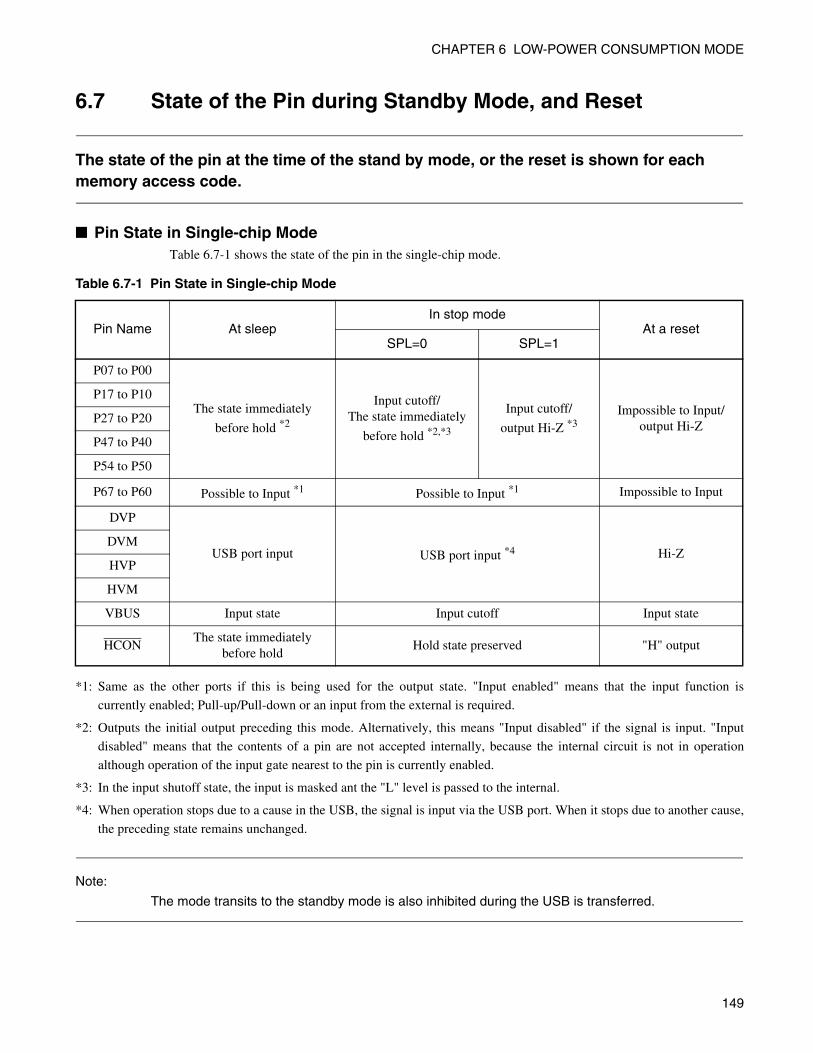
CHAPTER 6 LOW-POWER CONSUMPTION MODE
6.7 State of the Pin during Standby Mode, and Reset
The state of the pin at the time of the stand by mode, or the reset is shown for each memory access code.
Pin State in Single-chip ModeTable 6.7-1 shows the state of the pin in the single-chip mode.
*1: Same as the other ports if this is being used for the output state. "Input enabled" means that the input function is
currently enabled; Pull-up/Pull-down or an input from the external is required.
*2: Outputs the initial output preceding this mode. Alternatively, this means "Input disabled" if the signal is input. "Input
disabled" means that the contents of a pin are not accepted internally, because the internal circuit is not in operation
although operation of the input gate nearest to the pin is currently enabled.
*3: In the input shutoff state, the input is masked ant the "L" level is passed to the internal.
*4: When operation stops due to a cause in the USB, the signal is input via the USB port. When it stops due to another cause,
the preceding state remains unchanged.
Note:
The mode transits to the standby mode is also inhibited during the USB is transferred.
Table 6.7-1 Pin State in Single-chip Mode
Pin Name At sleepIn stop mode
At a resetSPL=0 SPL=1
P07 to P00
The state immediately
before hold *2
Input cutoff/The state immediately
before hold *2,*3
Input cutoff/
output Hi-Z *3Impossible to Input/
output Hi-Z
P17 to P10
P27 to P20
P47 to P40
P54 to P50
P67 to P60 Possible to Input *1 Possible to Input *1 Impossible to Input
DVP
USB port input USB port input *4 Hi-Z DVM
HVP
HVM
VBUS Input state Input cutoff Input state
HCONThe state immediately
before holdHold state preserved "H" output
149

CHAPTER 6 LOW-POWER CONSUMPTION MODE
6.8 Precautions when Using Low-power Consumption Mode
Special attention for the following is needed when using the low-power consumption mode.• Transition to standby mode and interrupt• Cancellation of standby mode by interrupt• Oscillation stabilization wait time• Switching clock mode• Notes on Accessing the Low-Power Consumption Mode Control Register (LPMCR) to
Enter the Standby Mode
Transition to Standby Mode and InterruptWhen there is the generation of an interrupt request to the CPU from the peripheral functions, the transition
to each standby mode is not made (the transition to the standby mode is not made even after the interrupt
processing) because even if you set "1" to the stop mode bit (STP) and the sleep mode bit (SLP) of the low-
power consumption mode control register (LPMCR), or "0" to the watch/timebase timer mode bit (TMD),
it is ignored. In this case, if the interrupt level is higher than 7, whether or not the interrupt request is
accepted by the CPU is not related to this operation.
Even when the CPU is currently performing interrupt processing, the device can go to the standby mode if
no other interrupt request is present with the interrupt request flag bit cleared.
Cancellation of Standby Mode by InterruptWhen an interrupt request with an interrupt level higher than 7 has been generated from a peripheral circuit,
etc. in sleep, timebase timer, or stop mode, standby mode is cleared. Whether or not the interrupt request is
accepted by the CPU is not related to this operation.
After the standby mode is canceled by the interruption, the operation is branched off to the interrupt
processing routine, if the priority of the interruption level set bit (IL2, IL1, IL0 bits of ICR register) to the
interrupt request is over the interrupt level mask register (ILM), and the interrupt is permitted by the I flag
of the condition cord register (CCR) (I=1). When an interrupt is not acceptable, processing from the
instruction succeeding the one which has specified standby mode continues.
When performing interrupt processing, interrupt processing normally transits after executing the instruction
succeeding the one specifying standby mode.
Depending on the conditions for transiting to standby mode, interrupt processing may starts before
executing the next instruction.
Note:
To prohibit a branch to the interrupt processing routine immediately after return, interrupts must beprohibited before standby mode is set.
150

CHAPTER 6 LOW-POWER CONSUMPTION MODE
Oscillation Stabilization Wait Time
Oscillation Stabilization Wait Time of oscillation clock
Because the oscillator for original oscillation is stopped in stop mode, the oscillation stabilization wait time
must be required. For the oscillation stabilization wait time, you take the time selected in the oscillation
stabilization wait time selection bit (WA1, WA0) of the clock selection register (CKSCR).
Note:
Be sure to set "00B" for the oscillation stabilization wait time selection bit (WS1, WS0) of the CKSCRregister ONLY at the time of the main clock.
Oscillation stabilization wait time of PLL clock
When the transition is made from a state where the CPU is operated by the main clock and the PLL clock
halts, to a mode where CPU and the peripherals are operated by the PLL clock, transition to the PLL clock
oscillation stabilization wait state is made and it is operated by the main clock during the oscillation
stabilization wait state.
The PLL clock oscillation stabilization wait time is fixed to 214/HCLK (HCLK: oscillation clock).
In PLL stop mode, the main clock and PLL multiplication circuit stop. During recovery from PLL stop
mode, it is necessary to allot the main clock oscillation stabilization wait time and PLL clock oscillation
stabilization wait time. The oscillation stabilization wait times for main clock and PLL clock are counted
simultaneously according to the value specified in the oscillation stabilization wait time selection bits
(CKSCR: WS1, WS0) in the clock selection register. The oscillation stabilization wait time selection bits
(CKSCR: WS1, WS0) in the clock selection register must be selected accordingly to account for the longer
of the main clock and PLL clock oscillation stabilization wait time. The PLL clock oscillation stabilization
wait time, however, requires 214/HCLK or more. Set the oscillation stabilization wait time selection bits
(CKSCR: WS1, WS0) in the clock selection register to "10B" or "11B".
Switching Clock ModeWhen switching of the clock mode is made, be sure not to change to other clock modes or the low-power
consumption mode until the completion of the switching. Completion of the switching can be checked by
referencing the MCM bit of the CKSCR. If the mode is switched to another clock mode or low-power-
consumption mode before completion of switching, the mode may not be switched.
151

CHAPTER 6 LOW-POWER CONSUMPTION MODE
Notes on Accessing the Low-Power Consumption Mode Control Register (LPMCR) to Enter the Standby Mode
To access the low-power consumption mode control register (LPMCR) with assembler language
• To set the low-power consumption mode control register (LPMCR) to enter the standby mode, use theinstruction listed in Table 6.3-2 "List of instructions used for transition to low-power consumption mode".
• The low-power consumption mode transition instruction in Table 6.3-2 "List of instructions used for transitionto low-power consumption mode" must always be followed by an array of instructions highlighted by a linebelow.
MOV LPMCR,#H'XX ; the low-power consumption mode transition instruction in Table 6.3-2
MOV A,#H'10 ; any instruction
The devices does not guarantee its operation after returning from the low-power consumption mode if youplace an array of instructions other than the one enclosed in the line.
To access the low-power consumption mode (LPMCR) with C language
To enter the standby mode using the low-power consumption mode control register (LPMCR), use one ofthe following methods (1) to (3) to access the register:
(1) Specify the standby mode transition instruction as a function and insert two _wait_nop() built-infunctions after that instruction. If any interrupt other than the interrupt to return from the standby modecan occur within the function, optimize the function during compilation to suppress the LINK andUNLINK instructions from occurring.
Example: Watch mode or timebase timer mode transition functionVoid enter_watch()
IO_LPMCR_byte = 0x10 /* Set LPMCR TMD bit to 0 */_wait_nop();_wait_nop();
(2) Define the standby mode transition instruction using _asm statements and insert two NOP and JMPinstructions after that instruction.
Example: Transition to sleep mode_asm(" MOV I: _IO_LPMCR,#H'58"); /* Set LPMCR SLP bit to 1 */_asm(" NOP");_asm(" NOP");_asm(" JMP $+3"); /* Jump to next instruction */
(3) Define the standby mode transition instruction between #pragma asm and #pragma endasm and inserttwo NOP and JMP instructions after that instruction.
Example: Transition to stop mode#pragma asm
MOV I: _IO_LPMCR,#H'98 /* Set LPMCR STP bit to 1 */NOPNOPJMP $+3 /* Jump to next instruction */
#pragma endasm
NOP
NOP
JMP $+3 ; jump to next instruction
152

CHAPTER 7MODE SETTING
This chapter describes the mode setting and the external memory access.
7.1 Mode Setting
7.2 Mode Pins (MD2 to MD0)
7.3 Mode Data
153

CHAPTER 7 MODE SETTING
7.1 Mode Setting
F2MC-16LX has respective modes in the access method, access area, and test. Respective mode is set according to the mode pin at the time of reset and the mode-fetched mode data.
Mode Setting
F2MC-16LX has respective modes in the access method, the access area, and the test, and Figure 7.1-1
shows the classification.
Figure 7.1-1 Classification of Mode
Operating ModeThe operation mode controls the operation state of the device and is specified by the mode setting pin
(MDx) and the contents of the Mx bit in the mode data. Selecting the operation mode, you may perform the
normal operation/the start of the internal test program/the start of the special test function.
Bus ModesThe bus mode controls the internal ROM operation and the external access function operation, and is
specified by the mode setting pin (MDx) and the contents of the Mx bit in the mode data. The mode setting
pin (MDx) specifies the bus mode to read the reset vector and the mode data. The Mx bit in the mode data
specifies the bus mode at the normal operation.
Operation mode Bus mode
RUN operation Single chip mode
FLASH write modeVarious test function mode
154

CHAPTER 7 MODE SETTING
7.2 Mode Pins (MD2 to MD0)
The mode pin is the three external pins (MD2 to MD0) and specifies the load methods for the reset vector and the mode data.
Setting of Mode Pins (MD2 to MD0)With the mode pin (MD2 to MD0), you may select either the external data bus or the internal data bus for
the reset vector read and select the bus width while selecting the external data bus. For the internal Flash
ROM products, the mode pin also specifies the Flash ROM write mode to write the internal ROM program
and so forth.
Table 7.2-1 shows the content of the mode pin setting.
Table 7.2-1 Content of Setting of Mode Pins
P61 P60 MD2 MD1 MD0 Mode NameReset vectors access area
External DataBus width
Remark
- - 0 0 0
Setting disabled- - 0 0 1
- - 0 1 0
- - 0 1 1 External vector mode Internal Mode DataOperation after reset
sequence is controlled with mode data
- - 1 0 0Setting disabled
- - 1 0 1
1 0 1 1 0 Flash serial writing
- - 1 1 1 Flash writer write mode - - -
Note:
MB90335 series can be used on the single chip mode only. Therefore, please set MD2:0=VSS andMD1, MD0:1=VCC.
155

CHAPTER 7 MODE SETTING
7.3 Mode Data
The mode data is located on the memory of the "FFFFDFH" address and specifies the
operation after the reset sequence. The mode data is automatically taken into the CPU by a mode fetch.
Mode DataWhile executing the reset sequence, the mode data in the "FFFFDFH" address is captured into the mode
register in the CPU core. CPU sets the memory access mode by this mode data. The values of the mode
register can be changed only in the reset sequence. The setting of the mode data is enabled after the reset
sequence.
Figure 7.3-1 shows the configuration of the mode data.
Figure 7.3-1 Bit Configuration of Mode Data
Set Bit of Bus Mode (M1, M0)The M1 and M0 bits specify the operation mode after the reset sequence.
Table 7.3-1 shows the content of the M1, M0 bit setting.
Note:
MB90335 series can be used on the single chip mode only. Please set M1, M0 = "00B".
Mode data
Bus setting bit Function extended bit(Reserved area)
7 6 5 4 3 2 1 0
M1 M0 0 0 0 0 0 0
Table 7.3-1 Content of M1 and M0 Bit Setting
M1 M0 Function
0 0 Single-chip mode
0 1 Internal ROM external bus modes
1 0 External ROM external bus modes
1 1 (Setting prohibited)
156

CHAPTER 7 MODE SETTING
Relation between Access Area and Physical AddressFigure 7.3-2 shows the relation between the access area and the physical address.
Figure 7.3-2 Relation between access Area and Physical address
Relation between Mode Pin and Mode Data (Recommended Example) Table 7.3-2 shows the relation between the mode pin and the mode data.
Note:
MB90335 series can be used on the single chip mode only.
FFFFFFH
00FFFFH
007FFFH
007900H
007100H
008000H
FF0000H
000100H
0000FBH
000000H
FFFFFFH
00FFFFH
007FFFH
007900H
001100H
008000H
FF0000H
000100H
0000FBH
000000H
FFFFFFH
00FFFFH
007FFFH
007900H
001100H
008000H
FF0000H
000100H
0000FBH
000000H
MB90V330A MB90F337 MB90337
Single chip mode (with ROM mirror function)
Peripheral area
ROM (FF bank)
ROM area(image of FF bank)
Register
RAM area (28 KB)
Peripheral area
Peripheral area
ROM (FF bank)
ROM area(image of FF bank)
Register
RAM area (4 KB)
Peripheral area
Peripheral area
ROM (FF bank)
ROM area(image of FF bank)
Register
RAM area (4 KB)
Peripheral area
Table 7.3-2 Relation between Mode Pin and Mode Data
Mode MD2 MD1 MD0 M1 M0
Single Chip 0 1 1 0 0
157

CHAPTER 7 MODE SETTING
158

CHAPTER 8I/O PORT
This chapter describes the configuration and functions of the register used in the I/O port.
8.1 Functions of I/O Ports
8.2 I/O Port Register
159

CHAPTER 8 I/O PORT
8.1 Functions of I/O Ports
The overview of the I/O ports is shown.
Functions of I/O PortsThe I/O port outputs data from the CPU to the I/O pin and loads the signal input in the I/O pin in the CPU
by using the port data register (PDR). In addition, the port can randomly set the direction of the input/
output of the I/O pin in bit unit by the port direction register (DDR).
The MB90335 Series has 37 input/output pins and 8 open drain output pins.
P07 to P00, P17 to P10, P27 to P20,P47 to P40, and P54 to P50 are I/O ports. P67 to P60 are open drain
pins.
160

CHAPTER 8 I/O PORT
8.2 I/O Port Register
The configuration and functions of the register used in the I/O port are described.
I/O Port RegistersThere are the following registers in I/O port.
• Port data register (PDR0 to PDR2, PDR4 to PDR6)
• Port direction register (DDR0 to DDR2, DDR4 to DDR6)
• Input resistance register (RDR0,RDR1)
• Output terminal register (ODR4)
161

CHAPTER 8 I/O PORT
8.2.1 Port Data Register (PDR0 to PDR2, PDR4 to PDR6)
The configuration and functions of the port data register (PDR0 to PDRB) are described.
Port Data Register (PDR0 to PDR2, PDR4 to PDR6) Figure 8.2-1 shows the list of the port data register (PDR0 to PDR2, PDR4 to PDR6).
Figure 8.2-1 List of Port Data Register (PDR0 to PDR2, PDR4 to PDR6)
Please note that the following operations are done.
• Input mode
- When reading: Read the level of the corresponding pin.
- When writing: Write into the latch for the input/output.
• Output mode
- When reading: Read the value of the data register latch.
- When writing: Output into the corresponding pin.
Initial value
15 14 13 12 11 10 9 8
7 6 5 4 3 2 1 0P07 P06 P05 P04 P03 P02 P01 P00 R/W *
PDR0XXXXXXXXB
AccessAddress : 000000H
P17 P16 P15 P14 P13 P12 P11 P10 R/W *PDR1
XXXXXXXXBAddress : 000001H7 6 5 4 3 2 1 0
P27 P26 P25 P24 P23 P22 P21 P20 R/W *PDR2
XXXXXXXXBAddress : 000002H
15 14 13 12 11 10 9 8
7 6 5 4 3 2 1 0P47 P46 P45 P44 P43 P42 P41 P40 R/W *
PDR4XXXXXXXXBAddress : 000004H
- - - P54 P53 P52 P51 P50 R/W *PDR5
---XXXXXBAddress : 000005H7 6 5 4 3 2 1 0
P67 P66 P65 P64 P63 P62 P61 P60 R/W *PDR6
XXXXXXXXBAddress : 000006H
*: The R/W access to the input/output port operates slightly different from the R/W access to the memory.
162

CHAPTER 8 I/O PORT
8.2.2 Port Direction Register (DDR0 to DDR2, DDR4 to DDR6)
The configuration and functions of the port direction register are described.
Port Direction Register (DDR0 to DDR2, DDR4 to DDR6) Figure 8.2-2 shows the list of the port direction register (DDR0 to DDR2, DDR4 to DDR6).
Figure 8.2-2 List of Port Direction Register (DDR0 to DDR2, DDR4 to DDR6)
When each terminal functions as a port
When each terminal functions as a port, controls the corresponding each terminal as follows.
• 0: Input mode.
• 1: Output mode reset sets to "0".
Note:
When accessing the DDR0 to DDR2, DDR4 to DDR6 registers by using the instruction of the readmodify write system (instructions such as bit set) is made, the bit targeted by an instruction becomesthe defined value, while the content of the output register set with the other bit changes to the inputvalue to the pin. Therefore, be sure to write an expected value into PDR firstly, and then set DDR,and finally change to the output when changing the input pin to the output pin is made.
Initial value
15 14 13 12 11 10 9 8
7 6 5 4 3 2 1 0D07 D06 D05 D04 D03 D02 D01 D00 R/W
DDR000000000B
AccessAddress : 000010H
D17 D16 D15 D14 D13 D12 D11 D10 R/WDDR1Address : 000011H
7 6 5 4 3 2 1 0D27 D26 D25 D24 D23 D22 D21 D20 R/W
DDR2Address : 000012H
15 14 13 12 11 10 9 8
7 6 5 4 3 2 1 0D47 D46 D45 D44 D43 D42 D41 D40 R/W
DDR4Address : 000014H
- - - D54 D53 D52 D51 D50 R/WDDR5Address : 000015H
7 6 5 4 3 2 1 0D67 D66 D65 D64 D63 D62 D61 D60 R/W
DDR6Address : 000016H
00000000B
00000000B
00000000B
---00000B
00000000B
163
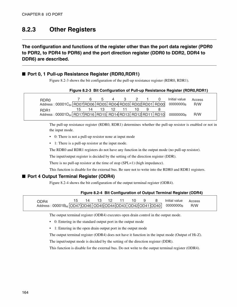
CHAPTER 8 I/O PORT
8.2.3 Other Registers
The configuration and functions of the register other than the port data register (PDR0 to PDR2, to PDR4 to PDR6) and the port direction register (DDR0 to DDR2, DDR4 to DDR6) are described.
Port 0, 1 Pull-up Resistance Register (RDR0,RDR1)Figure 8.2-3 shows the bit configuration of the pull-up resistance register (RDR0, RDR1).
Figure 8.2-3 Bit Configuration of Pull-up Resistance Register (RDR0,RDR1)
The pull-up resistance register (RDR0, RDR1) determines whether the pull-up resistor is enabled or not in
the input mode.
• 0: There is not a pull-up resistor none at input mode
• 1: There is a pull-up resistor at the input mode.
The RDR0 and RDR1 registers do not have any function in the output mode (no pull-up resistor).
The input/output register is decided by the setting of the direction register (DDR).
There is no pull-up resistor at the time of stop (SPL=1) (high impedance).
This function is disable for the external bus. Be sure not to write into the RDR0 and RDR1 registers.
Port 4 Output Terminal Register (ODR4)Figure 8.2-4 shows the bit configuration of the output terminal register (ODR4).
Figure 8.2-4 Bit Configuration of Output Terminal Register (ODR4)
The output terminal register (ODR4) executes open drain control in the output mode.
• 0: Entering in the standard output port in the output mode
• 1: Entering in the open drain output port in the output mode
The output terminal register (ODR4) does not have it function in the input mode (Output of Hi-Z).
The input/output mode is decided by the setting of the direction register (DDR).
This function is disable for the external bus. Do not write to the output terminal register (ODR4).
Initial value
15 14 13 12 11 10 9 8
7 6 5 4 3 2 1 0RD07 RD06 RD05 RD04 RD03 RD02 RD01 RD00 R/W
RDR000000000B
AccessAddress : 00001CH
R/WRDR1Address : 00001DH 00000000BRD17 RD16 RD15 RD14 RD13 RD12 RD11 RD10
Initial value15 14 13 12 11 10 9 8OD47 OD46 OD45 OD44 OD43 OD42 OD41 OD40 R/W
ODR400000000B
AccessAddress : 00001BH
164

CHAPTER 9TIMEBASE TIMER
This chapter describes the function and operation of the timebase timer.
9.1 Overview of Timebase Timer
9.2 Configuration of Timebase Timer
9.3 Timebase Timer Control Register (TBTC)
9.4 Interrupt of Timebase Timer
9.5 Operations of Timebase Timer
9.6 Precautions when Using Timebase Timer
9.7 Program Example of Timebase Timer
165

CHAPTER 9 TIMEBASE TIMER
9.1 Overview of Timebase Timer
The timebase timer has a interval timer function that enables a selection of four interval times using 18-bit free-run counter (timebase counter) count-up with synchronizing to the internal count clock (2 division of original oscillation). Furthermore, the function of timer output of oscillation stabilization wait time or function supplying operation clocks for watchdog timer are provided.
Interval Timer FunctionThe interval timer function generates interrupt requests at regular intervals.
• An overflow of the bit for the interval timer in the timebase counter generates an interrupt request.
• You can select one of four bits (interval time) for the interval timer.
Table 9.1-1 shows the interval time of the timebase timer.
Table 9.1-1 Interval Time of Timebase Timer
Internal count clock cycle Time of interval
2/HCLK (0.33 µs)
212/HCLK (Approx. 0.68 ms)
214/HCLK (Approx. 2.7 ms)
216/HCLK (Approx. 10.9 ms)
219/HCLK (Approx. 87.4 ms)
HCLK: Oscillation clockThe value in parentheses is applicable when the oscillation clock operates at 6 MHz.
166

CHAPTER 9 TIMEBASE TIMER
Function of Clock SupplyThe clock supply function supplies the operating clock to the timer for oscillation stabilization wait time
and some peripheral functions. Table 9.1-2 shows the clock cycle supplied from the timebase timer to each
peripheral.
Reference:
Because oscillation cycles is changeable after oscillation starts, the oscillation stabilization wait timeis listed for reference.
Table 9.1-2 Clock Cycles Supplied from Timebase Timer
Where to Supply Clock Clock Cycle Remark
Oscillation StabilizationWait Time
213/HCLK (Approx. 1.4 ms) Oscillation Stabilization Wait Time for ceramic oscillator
215/HCLK (Approx. 5.5 ms) Oscillation Stabilization Wait Time for crystal oscillator
217/HCLK (Approx. 21.8 ms)
Watchdog timer
212/HCLK (Approx. 0.68 ms)
Watchdog timer count up clock214/HCLK (Approx. 2.7 ms)
216/HCLK (Approx. 10.9 ms)
219/HCLK (Approx. 87.4 ms)
HCLK: Oscillation clockThe value in parentheses is applicable when the oscillation clock operates at 6 MHz.
167

CHAPTER 9 TIMEBASE TIMER
9.2 Configuration of Timebase Timer
The timebase timer consists of the following four blocks.• Timebase timer counter• Counter clear circuit• Interval timer selector• Timebase timer control register (TBTC)
Block Diagram of Timebase TimerFigure 9.2-1 shows the block diagram of the timebase timer.
Figure 9.2-1 Block Diagram of Timebase Timer
2 divisionof HCLK
Timebase timer counter
to PPG timer to Watchdog timer
Power-on resetStop mode start
to Oscillationstabilization wait time selectorin Clock controlunit
TBOF set
TBOF clear
Timebase timer control register(TBTC)
Timebase timer interrupt signal
UndefinedOverflowOscillation clockSwitch Machine clock to PLL clock from Main clock or Sub clock
Counter clear circuit
Interval timer selector
Reserved
OF OFOF OF
× 28× 21 × 22 × 23 × 29 × 210 × 211 × 212 × 213 × 214 × 215 × 216 × 217 × 218
TBIE TBOF TBR TBC1 TBC0
OFHCLK*
CKSCR : MCS = 1 0 *
168

CHAPTER 9 TIMEBASE TIMER
Timebase timer counter
This is an 18-bit up-counter whose count clock is two-division clock of oscillation clock (HCLK).
Counter clear circuit
This circuit clears the counter by writing "0" to timebase timer initialization bit (TBR) of timebase timer
control register (TBTC), power-on reset, transition to the stop mode, switching to PLL clock mode from the
main clock mode.
Interval timer selector
This selects the output of the timebase timer counter from one of four types. The overflow of selected bit
will be the interrupt cause.
Timebase timer control register (TBTC)
Interval time selection, counter clearance, and interrupt request control and status check are executed.
169

CHAPTER 9 TIMEBASE TIMER
9.3 Timebase Timer Control Register (TBTC)
The timebase timer control register (TBTC) executes interval time selection, timebase timer counter clearance, and interrupt control and status check.
Timebase Timer Control Register (TBTC)
Figure 9.3-1 Timebase Timer Control Register (TBTC)
Address
Reserved
Initial value
Interval time selection bit
Timebase timer initialization bit
Interrupt request flag bit
Interrupt request enable bit
Interrupt request output enables.
Interrupt request output disabled.
Read Write
Read Write
No change,no others are affected
No change,no others are affected
Clear Timebase timercounter, TBOF bit.
Always "1" is read.
Clear this bit.No overflow of specification bit
Overflow of specification bit
Always write this bit to "1".
Reserved bitReseved
The value in parentheses is applicable when the oscillation clock operates at 6 MHz.
: Readable/Writable: Write only: Undefined: Oscillation clock: Initial value
(Approx. 0.68 ms)
(Approx. 2.7 ms)
(Approx. 10.9 ms)
(Approx. 87.4 ms)
R/W WR/W R/W R/W
0000A9H
R/W
bit15 bit14 bit13 bit12 bit11 bit10 bit9 bit8 bit0
1--00100B (WDTC)
bit7
TBIE TBOF TBR TBC1 TBC0
TBC1 TBC0
212/HCLK
214/HCLK
216/HCLK
219/HCLK
0 0
0 0
0 0
1 1
TBR
0
1
TBOF
0
1
0
1
TBIE
R/WW
HCLK
170

CHAPTER 9 TIMEBASE TIMER
Table 9.3-1 Timebase Timer Control Register (TBTC)
Bit name Functions
bit15 Reserved: Reserved bit
Note:Be sure to write "1".
bit14 bit13
Unused bits • The value at the time of reading is irregular.• No effect on writing.
bit12 TBIE: Interrupt request enable bit
• This bit permits or prohibits an interrupt request output to the CPU.• If the TBIE bit and interrupt request flag bit (TBOF) is set to "1", an interrupt request is
output.
bit11 TBOF: Interrupt request flag bit
• An overflow of timebase timer counter specification bit sets the status to "1".• If the TBOF bit and interrupt request permission bit (TBIE) is set to "1", an interrupt request
is output.Setting to "0" executes clearance during writing and no changes are made at "1", making no influences on others.
Notes:• When clearing the TBOF bit, set to the condition that prohibits timebase timer interrupt with
the interrupt request permission bit (TBIE) or by specifying interrupt level mask register (ILM) in processor status (PS).
• The status is cleared to "0" by "0" writing, transition to the stop mode, transition from the main clock mode to the PLL clock mode, "0" writing to timebase timer initialization bit (TBR), or resetting.
bit10 TBR: Timebase timer initialization bit
• This bit clears the timebase timer counter.• Writing "0" clears the counter, immediately after that, clears the TBOF bit. No changes are
made at "1", making no influences on others.Reference:
Always read value is "1".
bit9 bit8
TBC1, TBC0: Interval time select bits
• These bits specify a cycle for the interval timer.• The bit for the interval timer of timebase timer counter is specified.• One of four interval time can be selected.
171

CHAPTER 9 TIMEBASE TIMER
9.4 Interrupt of Timebase Timer
The timebase timer can generate an interrupt request by the overflow of the specified bit of the timebase timer counter (interval timer function).
Interrupt of Timebase TimerAfter the timebase counter undergoes count-up with the internal count clock and the bit for the selected
interval timer overflows, the interrupt request flag bit (TBOF) of timebase timer control register (TBTC) is
set to "1". In this case, an interrupt request to CPU is generated if interrupt request is permitted by setting
the interrupt request permission bit (TBIE) is set to "1". Clear the interrupt request by writing "0" to the
TBOF bit in the interrupt processing routine. The TBOF bit is set when the specified bit overflows
regardless of the value of interrupt request permission bit (TBIE).
Note:
When clearing the interrupt request flag bit (TBOF) in the timebase timer control register (TBTC),perform while the timebase timer interrupt is prohibited by the setting of the interrupt level maskregister (IML) of the interrupt request permission bit (TBIE) or the processor status (PS).
References:
• When the TBOF bit is "1", an interrupt request is immediately generated upon the transition of theTBIE bit from prohibition to permission ("0" to "1").
• EI2OS and µDMAC cannot be used.
Interrupt of Timebase Timer and EI2OS, µDMAC
Table 9.4-1 shows the timebase timer interrupt and EI2OS, µDMAC.
Note:
ICR14 can be used for three interrupts, timebase timer interrupt, watch timer interrupt, and UARTreception end ch.0/1 interrupt, but the interrupt level is the same.
Table 9.4-1 Interrupt of Timebase Timer and EI2OS, µDMAC
Interrupt number
Interrupt level setting register Address in Vector TableEI2OS µDMAC
Register Name Address Low High Bank
#40 ICR14 0000BEH FFFF5CH FFFF5DH FFFF5EH
: Not available
172
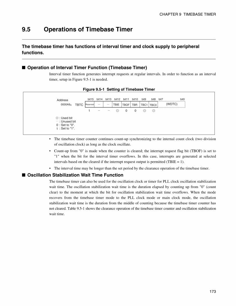
CHAPTER 9 TIMEBASE TIMER
9.5 Operations of Timebase Timer
The timebase timer has functions of interval timer and clock supply to peripheral functions.
Operation of Interval Timer Function (Timebase Timer)Interval timer function generates interrupt requests at regular intervals. In order to function as an interval
timer, setup in Figure 9.5-1 is needed.
Figure 9.5-1 Setting of Timebase Timer
• The timebase timer counter continues count-up synchronizing to the internal count clock (two division
of oscillation clock) as long as the clock oscillate.
• Count-up from "0" is made when the counter is cleared; the interrupt request flag bit (TBOF) is set to
"1" when the bit for the interval timer overflows. In this case, interrupts are generated at selected
intervals based on the cleared if the interrupt request output is permitted (TBIE = 1).
• The interval time may be longer than the set period by the clearance operation of the timebase timer.
Oscillation Stabilization Wait Time FunctionThe timebase timer can also be used for the oscillation clock or timer for PLL clock oscillation stabilization
wait time. The oscillation stabilization wait time is the duration elapsed by counting up from "0" (count
clear) to the moment at which the bit for oscillation stabilization wait time overflows. When the mode
recovers from the timebase timer mode to the PLL clock mode or main clock mode, the oscillation
stabilization wait time is the duration from the middle of counting because the timebase timer counter has
not cleared. Table 9.5-1 shows the clearance operation of the timebase timer counter and oscillation stabilization
wait time.
AddressReserved
: Used bit: Unused bit: Set to "0".: Set to "1".
bit15 bit14 bit13 bit12 bit11 bit10 bit9 bit8 bit7 bit0
0000A9H TBTC
1
1
(WDTC)
0
0 0
TBIE TBOF TBR TBC1 TBC0
173
CHAPTER 9 TIMEBASE TIMER
Function of Clock SupplyThe timebase timer supplies clock to the watchdog timer. The clearance of timebase counter effects the
operation of watchdog timer.
Table 9.5-1 Timebase Timer Counter Clearance Operation and Oscillation Stabilization Wait Time
OperationCounter
ClearTBOF Oscillation Stabilization Wait Time
Writing "0" to timebase timerinitialization bit (TBR) of timebase timercontrol register (TBTC)
None
Power-on reset
Main clock oscillation stabilization wait timeWatchdog reset ×
Release of main stop mode
Release of PLL stop mode
Transition from main clock mode to PLLclock mode (MCS=1 → 0)
PLL clock oscillation stabilization wait time
Release of timebase timer mode × × None
Release of sleep mode × × None
: Yes
× : None
174

CHAPTER 9 TIMEBASE TIMER
9.6 Precautions when Using Timebase Timer
Cautions about influences on peripheral functions due to interrupt request and timebase timer clearances.
Precautions when Using Timebase Timer
Clearing Interrupt request
When clearing the interrupt request flag bit (TBOF) in the timebase timer control register (TBTC), perform
while the timebase timer interrupt is masked by the setting of the interrupt level mask register (IML) of the
interrupt request permission bit (TBIE) or the processor status (PS).
Effect from timebase timer clear
By clearing the timebase timer counter, the following operations are affected.
• When using the interval timer function (interval interrupt) in the timebase timer
• When using the watchdog timer
Using timebase timer as oscillation stabilization wait time
After power on, since the oscillation clock halts in the main stop mode, oscillation stabilization wait time of
the oscillation clock will be needed using the operation clock supplied from the timebase timer after the
oscillator starts operating. Selection of suitable oscillation stabilization wait time is necessary depending on
the types of resonators connected to the high-speed oscillation pin. For details, see section "5.5 Oscillation
Stabilization Wait Time".
Notes on peripheral functions the timebase timer supplies to the clock
The mode that stops the main clock clears the counter, and then the timebase timer stops operation. The
clock supplied from the timebase timer may shorten the "H" level or lengthen the "L" level for up to 1/2
cycle because the clock is supplied from the initial state when the counter of the timebase timer is cleared.
The clock for the watchdog timer is also supplied from the initial status, however, the watchdog timer
operates in the normal cycles because the counter of the watchdog timer is cleared at the same time.
175

CHAPTER 9 TIMEBASE TIMER
Operations of Timebase TimerOperations in the following situations are shown in Figure 9.6-1.
• At a power-on reset occurs.
• At a transition to sleep mode during the operation of interval timer function
• At a transition to stop mode.
• At a counter clear request occurs.
The transition to the stop mode clears the timebase timer, terminating operations. Upon the recovery from
the stop mode, oscillation stabilization wait time is counted with the timebase timer.
Figure 9.6-1 Operations of Timebase Timer
Counter value
Oscillation stabilization wait overflow
Clear by transition to the stop mode
Power-on reset(Option)
Counter clearCPU operationstart
TBOF bit
TBIE bit
SLP bit(LPMCR register)
STP bit(LPMCR register)
Interval cycle
Sleep
StopInterval interrupt sleep cancellation
Stop cancellation by External interrupt
: Oscillation stabilization wait time: Oscillation clock
When setting "11B" to interval time selection bit (TBTC: TBC1, TBC0) of timebase timer control register (219/HCLK)
3FFFFH
00000H
(TBTC : TBC1, TBC0=11B) (TBTC : TBR=0)
HCLK
Clear by interrupt routine
176

CHAPTER 9 TIMEBASE TIMER
9.7 Program Example of Timebase Timer
Programming examples for the timebase timer are shown below.
Program Example of Timebase Timer
Processing specification
Interval interruptions of 212/HCLK (oscillation clock) are repeatedly generated. In this case, the interval
time is about 0.68 ms (at 6-MHz operation).
Coding example
ICR14 EQU 0000BEH ; Interrupt control register for timebase timer
TBTC EQU 0000A9H ; Timebase timer control register
TBOF EQU TBTC:3 ; Interrupt request flag bit
;----------Main Program----------------------------------------------------
CODE CSEG
START:
; : ; Initialize such as a stack pointer (SP)
AND CCR, #0BFH ; Disables the interrupt
MOV I:ICR14, #00H ; Interrupt level 0 (highest)
MOV I:TBTC, #10010000B ; Upper 3 bits fixed
; Interrupt enabled, TBOF Clear
; Counter Clear
; Interval Time Selection 212/HCLK selection
MOV ILM, #07H ; Sets ILM in PS to level 7
OR CCR, #40H ; Interruption permission
LOOP: MOV A,#00H ; infinite loop
MOV A,#01H
BRA LOOP
;----------Interrupt Program----------------------------------------------------
WARI:
CLR bit BOF ; The interrupt request flag is clear
; :
; User processing
; :
RETI ; Returns from interrupt
CODE ENDS
;----------Vector Settings----------------------------------------------------------
VECT CSEG ABS=0FFH
177

CHAPTER 9 TIMEBASE TIMER
ORG 0FF6CH ; The interruption vector is set
DSL WARI
ORG 0FFDCH ; Reset vector setting
DSL START
DB 00H ; Single-chip mode
VECT ENDS
END START
178

CHAPTER 10WATCHDOG TIMER
This chapter describes the function and operation of the watchdog timer.
10.1 Overview of Watchdog Timer
10.2 Watchdog Timer Control Register (WDTC)
10.3 Configuration of Watchdog Timer
10.4 Operations of Watchdog Timer
10.5 Precautions when Using Watchdog Timer
10.6 Program Examples of Watchdog Timer
179

CHAPTER 10 WATCHDOG TIMER
10.1 Overview of Watchdog Timer
The watchdog timer is a 2-bit counter operating with an output of the timebase timer or clock timer as the count clock and resets the CPU when the counter is not cleared for a preset period of time.
Functions of Watchdog TimerThe watchdog timer is a counter for preventing programs from hanging up. The timer must be cleared at
specified intervals after being activated. If the watchdog timer is not cleared within a certain time due to an
infinite loop of the program, etc., a watchdog reset is generated to the CPU. The interval time of the
watchdog timer can be set by the watchdog timer control register (WDTC), as shown in Table 10.1-1.
When the watchdog timer is not cleared, a watchdog reset occurs following the time between the minimum
time interval and the maximum time interval. The counter must be cleared within the time of the minimum
time interval.
Note:
The watchdog counter is a 2-bit counter that counts carry-up signals from the timebase timer.Therefore, when the timebase timer is cleared, the time period until the occurrence of a watchdogtimer reset may be longer than the preset period of time.
Reference:
When the watchdog timer is activated, it is initialized and set to the stopped state by a reset uponpower-on or by a reset by the watchdog. Also, the watchdog counter is cleared by writing to the resetby the external pin, the software reset, and the watchdog control bit (WTE) of the watchdog timercontrol register and by changing to sleep and stop mode, but the watchdog timer is still activated.
Table 10.1-1 Interval Time of Watchdog Timer
WT1 WT0 Interval Time
Clock cycle numberMin. * Max. *
0 0 Approx. 2.39 ms Approx. 3.07 ms 214 ± 211/HCLK
0 1 Approx. 9.56 ms Approx. 12.29 ms 216 ± 213/HCLK
1 0 Approx. 38.23 ms Approx. 49.15 ms 218 ± 215/HCLK
1 1 Approx. 305.83 ms Approx. 393.22 ms 221 ± 218/HCLK
*: Value for when operating at oscillator clock (HCLK) of 6 MHz. The maximum and minimum watchdog timer interval time and the number of oscillation clock cycles are determined by the timing of clear operation. The interval time will be 3.5 to 4.5 times of the count clock (supplied clock of timebase timer) cycle. For the watchdog timer interval time, see "10.4 Operations of Watchdog Timer".
180
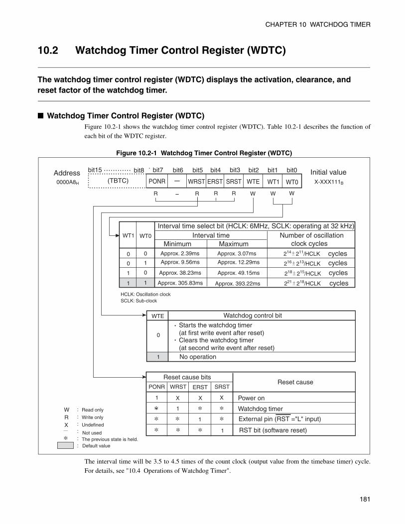
CHAPTER 10 WATCHDOG TIMER
10.2 Watchdog Timer Control Register (WDTC)
The watchdog timer control register (WDTC) displays the activation, clearance, and reset factor of the watchdog timer.
Watchdog Timer Control Register (WDTC)Figure 10.2-1 shows the watchdog timer control register (WDTC). Table 10.2-1 describes the function of
each bit of the WDTC register.
Figure 10.2-1 Watchdog Timer Control Register (WDTC)
The interval time will be 3.5 to 4.5 times of the count clock (output value from the timebase timer) cycle.
For details, see "10.4 Operations of Watchdog Timer".
Address Initial value
Interval time select bit (HCLK: 6MHz, SCLK: operating at 32 kHz)Number of oscillation clock cycles
Interval timeMinimum Maximum
cyclescyclescycles
cycles
Approx. 2.39ms Approx. 3.07ms
Approx. 9.56ms Approx. 12.29ms
Approx. 38.23ms Approx. 49.15ms
Approx. 305.83ms Approx. 393.22ms
HCLK: Oscillation clockSCLK: Sub-clock
Watchdog control bit
Starts the watchdog timer(at first write event after reset)Clears the watchdog timer(at second write event after reset)No operation
Reset cause bitsReset cause
Power on
Watchdog timer
External pin (RST ="L" input)
RST bit (software reset)
Read only
Write only
Undefined
Not usedThe previous state is held.Default value
0000A8H
bit15
X-XXX111B (TBTC)
bit7 bit6 bit5 bit4 bit3 bit2 bit1 bit0bit8
WR R R R W W
PONR WRST ERST SRST WTE WT1 WT0
214 211/HCLK
216 213/HCLK
218 215/HCLK
221 218/HCLK
0
1
0
1
0
0
1
1
WT1 WT0
WTE
0
1
PONR ERSTWRST SRST
1
1
1
1
X X X
XRW
181

CHAPTER 10 WATCHDOG TIMER
Table 10.2-1 Function of Each Bit of Watchdog Timer Control Register (WDTC)
Bit name Functions
bit7 bit5 bit4 bit3
PONR WRST ERST SRST
Reset factor bit
• Read-only bits that indicate reset factors. When a reset factor occurs, therelevant bit is set to "1".
• The PONR, WRST, ERST and SRST bits are all cleared to "0" after theWDTC register is read.
• The contents of the bits other than the PONR bit are not assured at power-on.Therefore, when the PONR bit is "1", ignore the contents of the bits otherthan the PONR bit.
bit6 Reserved Reserved bit• The reading value is irregular.• Writing does not have the influence in the operation.
bit2 WTE Watchdog control bit
• Writing "0", activates the watchdog timer (at the first write after reset) orclears the 2-bit counter (at the second write after reset).
• There is no influence in the operation in writing "1".
bit1bit0
WT1 WT0
Interval time select bit
• This is a bit to select the interval time of the watchdog timer.• The data at the activation of the watchdog timer is valid. Data written after
the activation of the watchdog timer is ignored.• The WT1 and WT0 bit are only for writing.
182

CHAPTER 10 WATCHDOG TIMER
10.3 Configuration of Watchdog Timer
The watchdog timer consists of following five blocks.• Count clock selector• Watchdog counter (two bits counter)• Watchdog reset generator circuit• Counter clear control circuit• Watchdog timer control register (WDTC)
Block Diagram of Watchdog TimerFigure 10.3-1 shows a watchdog timer block diagram.
Figure 10.3-1 Block Diagram of Watchdog Timer
Count clock selector
Circuit that selects the count clock of the watchdog timer from four types of timebase timer output and four
types of watch timer output. This determines the watchdog reset generation time.
Watchdog counter (two bits counter)
2-bit up-counter that uses timebase timer output as the count clock.
Watchdog reset generator circuit
Generates a reset signal by an overflow of the watchdog counter.
Counter clear control circuit
Clears the watchdog counter and controls operation/stop of the counter.
Watchdog timer control register (WDTC)
Activates/clears the watchdog timer and holds the reset occurrence factor.
Watchdog timer control register (WDTC)
Timebase timer mode startSleep mode start
Stop mode start
Watchdog timer
Counterclear control
circuit
Counterclock
selector
Watchdog resetgeneration
circuit
Watchdogcounter
Over-flow
CLR and Activation
to Internal resetgeneration circuit
Clear
(Timebase timer counter)
2 divided of HCLK
HCLK: Oscillation clock
2
CLR
WRST ERST SRST WTE WT1 WT0PONR
CLR
4
4
21 22 28 21829 210 211 212 213 214 215 216 217
183

CHAPTER 10 WATCHDOG TIMER
10.4 Operations of Watchdog Timer
The watchdog timer generates a watchdog reset upon an overflow of the watchdog counter.
Operations of Watchdog TimerFigure 10.4-1 shows the setting required to operate the watchdog timer.
Figure 10.4-1 Setting of Watchdog Timer
Activating watchdog timer
• The watchdog timer is activated at the first write of "0" to the watchdog control bit (WTE) of the
watchdog timer control register (WDTC) after reset. In this case, specify the interval time at the same
time by the interval time selection bits (WT1, WT) of the WDTC register.
• Once the watchdog time is activated, it cannot stop until power-on or a watchdog reset occurs.
Clearing watchdog timer
• The 2-bit counter of the watchdog timer is cleared by the second write of "0" to the WTE bit. If the
counter is not cleared within the interval time, the counter overflows and the watchdog is reset.
• The watchdog counter is cleared when a reset operation occurs or when a change to sleep mode, stop
mode or timebase timer mode is made.
• When a change to timebase timer mode is made, the watchdog counter is once cleared. However, be
careful that the watchdog counter does not stop after being cleared.
Interval Time of Watchdog Timer
Figure 10.4-2 shows the relationship between watchdog timer clear timing and interval time. The interval
time varies depending on the timing of clearing the watchdog timer and takes 3.5 to 4.5 times of the count
clock cycle.
Checking reset factors
By checking the reset factor bit (PONR, WRST, ERST, SRST) of the WDTC register after reset, the factor
of the reset can be identified.
Used bitUnused bitSet to "0".
Address bit15 bit7 bit6 bit5 bit4 bit3 bit2 bit1 bit0
PONR(TBTC)0000A8H WDTC
bit8
WRST ERST SRST WTE WT1
0
0
WT0
184

CHAPTER 10 WATCHDOG TIMER
Figure 10.4-2 Relationship between Clear Timing and Interval Time of Watchdog Timer
[Block diagram of Watchdog timer]
[Minimum interval time]
[Maximum interval time]
2-bit counter
2 dividedcircuitClock selector 2 divided
circuit Reset circuit Reset signal
Count enable and clearCount enableoutput circuitWTE bit
Count startCounter clear
Count startCounter clear
Count clock a
2 divided value b
2 divided value c
Count enable
Reset signal d
Count clock a
2 divided value b
2 divided value c
Count enable
Reset signal d
WTE bit clear
WTE bit clear
Watchdog reset generation
Watchdog reset generation
(Count clock cycle/2)
(Count clock cycle/2)
When clear WTE bit immediately before rising of count clock
When clear WTE bit immediately after rising of count clock
a b c
7
7
d
185

CHAPTER 10 WATCHDOG TIMER
10.5 Precautions when Using Watchdog Timer
This section explains precautions when using watchdog timer.
Precautions when Using Watchdog Timer
Stopping watchdog timer
Once the watchdog time is activated, it cannot stop until power-on or a watchdog-external reset occurs.
Interval Time
Because the interval time uses carry-up signals from the timebase timer, as the count clock, clearing the
timebase timer may make the interval time of the watch dog timer longer than the preset period of time.
Selecting Interval Time
The interval time can be set when activating the watchdog timer. Data written after the activation of the
watchdog timer is ignored.
Precautions when creating program
When creating a program that clears the watchdog timer repeatedly in the main loop, the main loop
processing time including the interrupt processing must not exceed the minimum interval time of the
watchdog timer.
186

CHAPTER 10 WATCHDOG TIMER
10.6 Program Examples of Watchdog Timer
Program example of watchdog timer is given below.
Program Examples of Watchdog Timer
Processing specification
• The watchdog timer is cleared each time in loop of the main program.
• The processing of the main loop must go round within the minimum interval time.
Coding example
WDTC EQU 0000A8H ; Watchdog timer control register
WTE EQU WDTC:2 ; Watchdog timer control bit
;----------Main program---------------------------------------------------
CODE CSEG
START:
; : ; Initialize such as a stack pointer (SP).
WDG_START:
MOV WDTC, #00000011B ; Activating watchdog timer
; 221 ± 218 cycles in time of the interval are selected.
;----------Main loop-------------------------------------------------------
MAIN: CLRB I:WTE ; Clearing watchdog timer
; : It is regularly clearness of two bits.
; User processing
; :
JMP MAIN ; Interval Time of Watchdog Timer
; Loop in the shortest possible time
CODE ENDS
;----------Vector Settings---------------------------------------------------------
VECT CSEG ABS=0FFH
ORG 0FFDCH ; Reset vector setting
DSL START
DB 00H ; Single-chip mode setting
VECT ENDS
END START
187

CHAPTER 10 WATCHDOG TIMER
188

CHAPTER 11USB FUNCTION
This chapter describes the functions and overview of the USB Function.
11.1 Overview of USB Function
11.2 Block Diagram of USB Function
11.3 Register of USB Function
11.4 Operation Explanation of USB Function
189
CHAPTER 11 USB FUNCTION
11.1 Overview of USB Function
The USB Function is an interface that supports the USB (Universal Serial Bus) communication protocol. It operates supporting the transfer speed of FULL (12 Mbps) and has the following characteristics.
Features of USB Function• FULL speed (12 Mbps) is supported. (conform to USB2.0 Full Speed.)
• The device status is auto-answer.
• Bit string, bit stuffing, and automatic generation and check of CRC5 and CRC16
• Toggle check by data synchronization bit
• Automatic response to all standard commands except Get/SetDescriptor and SynchFrame commands
(these three commands can be processed the same way as the class vendor commands.)
• The class vendor commands can be received as data and responded via firmware.
• Support up to six EndPoints (EndPoint0 is fixed to control transfer.)
• 2 built-in transfer data buffers for each EndPoint (each of two built-in buffers dedicated to IN and OUT,
respectively, for EndPoint0)
• Support automatic transfer mode for transfer data via DMA (except buffers for EndPoint0)
190

CHAPTER 11 USB FUNCTION
11.2 Block Diagram of USB Function
Figure 11.2-1 shows the USB Function block diagram.
Block Diagram of USB Function
Figure 11.2-1 Block Diagram of USB Function
DVP
DVM
UDC
Pin
US
B D
RV
#11,12
SPT
SUSP
Internal data bus
Interrupt
UDOinterfaceCLK(48MHz)
Interrupt #13
Interrupt #14
CPU interface
UDCC registerUDCS register
Timestamp
EndPoint0In buffer
EndPoint0Out buffer
EndPoint1buffer
EndPoint2buffer
EndPoint3buffer
EndPoint4buffer
EndPoint5buffer
191

CHAPTER 11 USB FUNCTION
11.3 Register of USB Function
The configuration and functions of registers used in the USB Function are described.
Register List of USB Function
Figure 11.3-1 Register List of USB Function
15 8 7 0
UDCC (R/W)
EP0C (R/W)
EP1C (R/W)
EP2C (R/W)
EP3C (R/W)
EP4C (R/W)
EP5C (R/W)
TMSP (R)
UDCIE UDCS (R/W)
EP0IS (R/W)
EP0OS (R/W)
EP1S (R/W)
EP2S (R/W)
EP3S (R/W)
EP4S (R/W)
EP5S (R/W)
EP0DT (R/W)
EP1DT (R/W)
EP2DT (R/W)
EP3DT (R/W)
EP4DT (R/W)
EP5DT (R/W)
8 bits 8 bits
192

CHAPTER 11 USB FUNCTION
Figure 11.3-2 Register of USB Function
bit 7 6 5 4 3 2 1 0
Address:0000D0H RST RESUM HCON USTP Reserved Reserved RFBK PWC UDC control register (UDCC)
bit 15 14 13 12 11 10 9 8 Address:0000D1H Reserved Reserved Reserved Reserved Reserved Reserved Reserved Reserved
bit 7 6 5 4 3 2 1 0 Address:0000D2H Reserved PKS0 EP0 control register (EP0C)
bit 15 14 13 12 11 10 9 8 Address:0000D3H - - - - Reserved Reserved STAL Reserved
bit 7 6 5 4 3 2 1 0 Address:0000D4H PKS EP1 control register (EP1C)
bit 15 14 13 12 11 10 9 8 Address:0000D5H EPEN TYPE DIR DMAE NULE STAL PKS1
bit 7 6 5 4 3 2 1 0 Address:0000D6H Reserved PKS EP2 control register (EP2C)
bit 15 14 13 12 11 10 9 8 Address:0000D7H EPEN TYPE DIR DMAE NULE STAL Reserved
bit 7 6 5 4 3 2 1 0 Address:0000D8H Reserved PKS EP3 control register (EP3C)
bit 15 14 13 12 11 10 9 8 Address:0000D9H EPEN TYPE DIR DMAE NULE STAL Reserved
bit 7 6 5 4 3 2 1 0 Address:0000DA
HReserved PKS EP4 control register (EP4C)
bit 15 14 13 12 11 10 9 8 Address:0000DB
HEPEN TYPE DIR DMAE NULE STAL Reserved
bit 7 6 5 4 3 2 1 0 Address:0000DC
HReserved PKS EP5 control register (EP5C)
bit 15 14 13 12 11 10 9 8 Address:0000DD
HEPEN TYPE DIR DMAE NULE STAL Reserved
bit 7 6 5 4 3 2 1 0 Address:0000DE
HTMSP Time stamp register (TMSP)
bit 15 14 13 12 11 10 9 8 Address:0000DFH - - - - - TMSP
bit 7 6 5 4 3 2 1 0 Address:0000E0H - - SUSP SOF BRST WKUP SETP CONF UDC status register (UDCS)
bit 15 14 13 12 11 10 9 8
Address:0000E1H Reserved Reserved SUSPIE SOFIE BRSTIE WKUPIE CONFN CONFIE UDC interruption permission register (UDCIE)
bit 7 6 5 4 3 2 1 0 Address:0000E2H - - - - - - - - EP0I status register (EP0IS)
bit 15 14 13 12 11 10 9 8 Address:0000E3H BFINI DRQIIE - - - DRQI - -
bit 7 6 5 4 3 2 1 0
Address:0000E4H Reserved SIZE EP0O status register (EP0OS)
bit 15 14 13 12 11 10 9 8 Address:0000E5H BFINI DRQOIE SPKIE - - DRQO SPK Reserved
Continued
193

CHAPTER 11 USB FUNCTION
Continued
7 6 5 4 3 2 1 0
Address:0000E6H SIZE EP1 status register (EP1S)
bit 15 14 13 12 11 10 9 8
Address:0000E7H BFINI DRQIE SPKIE Reserved BUSY DRQ SPK SIZE
bit 7 6 5 4 3 2 1 0
Address:0000E8H Reserved SIZE EP2 status register (EP2S)
bit 15 14 13 12 11 10 9 8
Address:0000E9H BFINI DRQIE SPKIE Reserved BUSY DRQ SPK Reserved
bit 7 6 5 4 3 2 1 0
Address:0000EAH Reserved SIZE EP3 status register (EP3S)
bit 15 14 13 12 11 10 9 8
Address:0000EBH BFINI DRQIE SPKIE Reserved BUSY DRQ SPK Reserved
bit 7 6 5 4 3 2 1 0
Address:0000ECH Reserved SIZE EP4 status register (EP4S)
bit 15 14 13 12 11 10 9 8
Address:0000EDH BFINI DRQIE SPKIE Reserved BUSY DRQ SPK Reserved
bit 7 6 5 4 3 2 1 0
Address:0000EEH Reserved SIZE EP5 status register (EP5S)
bit 15 14 13 12 11 10 9 8
Address:0000EFH BFINI DRQIE SPKIE Reserved BUSY DRQ SPK Reserved
bit 7 6 5 4 3 2 1 0
Address:0000F0H BFDT EP0 data register (EP0DT)
bit 15 14 13 12 11 10 9 8
Address:0000F1H BFDT
bit 7 6 5 4 3 2 1 0
Address:0000F2H BFDT EP 1 data register (EP1DT)
bit 15 14 13 12 11 10 9 8
Address:0000F3H BFDT
bit 7 6 5 4 3 2 1 0
Address:0000F4H BFDT EP 2 data register (EP2DT)
bit 15 14 13 12 11 10 9 8
Address:0000F5H BFDT
bit 7 6 5 4 3 2 1 0
Address:0000F6H BFDT EP 3 data register (EP3DT)
bit 15 14 13 12 11 10 9 8
Address:0000F7H BFDT
bit 7 6 5 4 3 2 1 0
Address:0000F8H BFDT EP 4 data register (EP4DT)
bit 15 14 13 12 11 10 9 8
Address:0000F9H BFDT
bit 7 6 5 4 3 2 1 0
Address:0000FAH BFDT EP 5 data register (EP5DT)
bit 15 14 13 12 11 10 9 8
Address:0000FBH BFDT
194

CHAPTER 11 USB FUNCTION
11.3.1 UDC Control Register (UDCC)
UDC control register (UDCC) controls the UDC core circuit.
UDC Control Register (UDCC) Figure 11.3-3 shows the bit configuration of the UDC control register (UDCC).
Note:
You must set the UDC control register (UDCC) when RST of bit7 is 1 except bit6 or RESUM of bit6and USTP of bit4, and never rewrite it while USB is operating. Set and reset RESUM of bit6 onlywhen USB is in suspend status and gets in remote Wake-up enabled status with the followingcommand:
Set USTP of bit4 to "1" before entering the stop mode state.
To deselect the stop mode, set the order of SUSP and USTP in the UDCC to "0".
The following describes the function of each bit in the UDC control register (UDCC).
[bit15 to bit8] Reserved bit
These bit are reserved bit. Please wright "0". The bit always reads "0".
[bit7] RST: Function reset bit
Apply an individual reset that is equivalent to the system reset to the chip to the USB Function. Apply a
reset to the USB Function with the RST bit when connecting a cable to the HOST PC. Since the RST
bit has the initial value of "1" and the USB Function is in reset status, release the Function by writing
"0" to the bit.
Figure 11.3-3 UDC Control Register (UDCC)
Address bit 7 6 5 4 3 2 1 0
0000D0H RST RESUM HCON USTP Reserved Reserved RFBK PWC UDC control register
1 0 1 0 0 0 0 0 ← Initial value
R/W R/W R/W R/W - - R/W R/W ← Access
Address bit 15 14 13 12 11 10 9 8
0000D1H Reserved Reserved Reserved Reserved Reserved Reserved Reserved Reserved
0 0 0 0 0 0 0 0 ← Initial value
- - - - - - - - ← Access
RST Operating mode
0 Reset of USB Function release
1 Reset USB Function
195
CHAPTER 11 USB FUNCTION
Note:
The RST bit initializes the corresponding bits of the timestamp register, UDC status register, andinterrupt enable register at once. In addition, since it sets EP0I, EP0O, and BFINIs of EP1 to EP5status registers at the same time after initialization, clear the RST bit (which does not clear the BFINIbits), and clear the BFINI of an endpoint to be used in this sequence.
[bit6] RESUM: Resume setting bit
When it is in remote Wake-up enabled status (or DEVICE_REMOTE_WAKEUP bit is set with the
SET_FEATURE command by the host) and in suspend status, the resume operation is started by writing
1 to the RESUM bit. Clear the resume direction by writing "0" to the RESUM bit that was set to "1".
[bit5] HCON: Host connection bit
Control a switch between an external pull-up resistor and the USB data line and allows the USB
Function to recognize connections to HOST PC or HUB.
Note:
Even if the external pull-up resistor is HOST at the state of ON or the connection is recognized fromthe HUB, the bus reset and the command of the USB bus ignores when the HCON bit is set to "1".
[bit4] USTP:USB operation clock stop bit
Stop the clock of the USB operation part by setting the USTP bit. Setting the USTP bit can reduce
power consumption when keeping the USB out of service.
RESUM Operating mode
0 USB resume start dictating bit release
1 USB resume start dictate
HCON Operating mode
0 HOST PC or HUB and connection
1 HOST PC or HUB and state of cutting
USTP Operating mode
0 Normal mode
1 Clock stop of USB operation part
196

CHAPTER 11 USB FUNCTION
Note:
If the USTP bit is not used in the stop mode, wait for 3 cycles or 43 cycles to elapse in FULL speedor in LOW speed (that is supported only in Mini-HOST mode) so that you can ensure that the resetoperation will function when you have set RST=1. You may clear the USTP bit and the RST bit atonce.
[bit3, bit2] Reserved bit
It is reserved bit. Please write "0". The bit always reads "0".
[bit1] RFBK: Data toggle mode selection bit (rate feedback mode)
It is a bit that selects data toggle mode for USB Interrupt transfer.
The data toggle mode selection can be used for rate feedback information in ISO transfer.
[bit0] PWC: Power supply control bit
It specifies the operating power supply mode (self power or bus power) for the USB Function.
(The setting of the PWC bit is reflected in the standard command GetStatus.)
RFBK Operating mode
0 Selection of alternation data toggle modeIt toggles a data PID when a transfer has been successfully completed.
1Selection of data toggle modeIt is a toggle the data PID in unconditional.
PWC Operating mode
0 Bus power
1 Self power
197

CHAPTER 11 USB FUNCTION
11.3.2 EP0 Control Register (EP0C)
EP0 control register (EP0C) controls concerning end point 0.
EP0 Control Register (EP0C) Figure 11.3-4 shows the bit configuration of the EP0 control register (EP0C).
Note:
Ensure that you must set the EP0 control register (EP0C), except bit9 STAL, when both bit7 RST ofthe UDC control register (UDCC) and bit7 BFINI of the EP0I/EP0O status register (EP0IS/EP0OS)are 1 and must not rewrite it while the USB is operating.
The following describes the function of each bit in the EP0 control register (EP0C).
[bit15 to bit12] Undefined bit
Writing has no effect on the operation. Reading is indeterminate.
[bit11, bit10] Reserved bit
It is reserved bit. Please write "0".
The bit always reads "0" when read.
[bit9] STAL:STALL EndPoint0 set bit
Setting the STAL bit can put EndPoint0 in STALL status (STALL response).
Note:
The STALL response is continued to the host while the STAL bit is set. The USB Function returnsfrom STALL status when it receives a normal SETUP packet after the STAL bit is deselected.
Figure 11.3-4 EP0 Control Register (EP0C)
Address bit 7 6 5 4 3 2 1 0
0000D2H Reserved PKS0 EP0 control register
0 1000000 ← Initial value
- R/W ←Access
Address bit 15 14 13 12 11 10 9 8
0000D3H - - - - Reserved Reserved STAL Reserved
X X X X 0 0 0 0 ←Initial value
- - - - - - R/W - ←Access
STAL Operating mode
0 Release of state of STALL
1 Set of state of STALL (STALL response)
198

CHAPTER 11 USB FUNCTION
[bit8, bit7] Reserved bit
It is reserved bit. Please write "0".
The bit always reads "0" when read.
[bit6 to bit0] PKS0:Packet size end point 0 set bit
It specifies the maximum number of transfer bytes per packet. The maximum number of transfer bytes
per packet that EndPoint0 can specify is 64 bytes, which is a setting common to IN and OUT.
<Example> "08H"→8 Byte, "40H"→64 Byte (maximum specified value)
Note:
Setting a value not less than the maximum number of transfer bytes (40H) and "00H" is forbidden.
199

CHAPTER 11 USB FUNCTION
11.3.3 EP1 to EP5 Control Register (EP1C to EP5C)
EP1 to EP5 control register (EP1C to EP5C) controls concerning end point 1 to 5.
EP1 to EP5 Control Register (EP1C to EP5C) Figure 11.3-5 shows the bit configuration of the EP1C to EP5C control register (EP1C to EP5C).
Note:
Ensure that you must set the EP1 to EP5 control registers (EP1C to EP5C), except DMAE, NULE,and STAL, when both bit7 RST of the UDC control register (UDCC) and bit15 BFINI of the EP0 toEP5 status registers (EP1S to EP5S) are 1 and must not rewrite them while the USB is operating.
The following describes the function of each bit in the EP1 to EP5 control register (EP1C to EP5C).
Figure 11.3-5 EP1 to EP5 Control Register (EP1C to EP5C)
Address bit 7 6 5 4 3 2 1 0
EP1C 0000D4H PKS1
0 0 0 0 0 0 0 0 ← Initial value
R/W R/W R/W R/W R/W R/W R/W R/W ← Access
Address bit 7 6 5 4 3 2 1 0
EP2C 0000D6H EP3C 0000D8H
EP4C 0000DAH EP5C 0000DCH
Reserved PKS5 to PKS2
0 1 0 0 0 0 0 0 ← Initial value
- R/W R/W R/W R/W R/W R/W R/W ← Access
Address bit 15 14 13 12 11 10 9 8
EP1C 0000D5H EPEN TYPE DIR DMAE NULE STAL PKS1
0 1 1 0 0 0 0 1 ← Initial value
R/W R/W R/W R/W R/W R/W R/W R/W ← Access
Address bit 15 14 13 12 11 10 9 8
EP2C 0000D7H EP3C 0000D9H EP4C 0000DBH EP5C 0000DDH
EPEN TYPE DIR DMAE NULE STAL Reserved
0 1 1 0 0 0 0 0 ← Initial value
R/W R/W R/W R/W R/W R/W R/W - ← Access
200
CHAPTER 11 USB FUNCTION
[bit15] EPEN: End Point 1 to 5 permission bit
The end point is made effective. Setting the EPEN bit allows it to be configures by the host as an endpoint for use in the USB Function. TYPE, DIR, and PKS of the EP1 to EP5 control registers becomevalid for configuration information.
[bit14, bit13] TYPE: End point forwarding type selection bit
The forwarding type supported by the end point is specified.
[bit12] DIR: End point forwarding direction selection bit
It specifies a transfer direction that the end point supports.
[bit11] DMAE: DMA automatic transfer enable bit
It is a mode setting that uses DMA for read and write operations to transmit and receive buffers fortransfer data and automatically transfers transmit and receive data in sync with IN and OUT datarequests from the HOST until data whose pieces are as many as the number of transfer data set in DMAis transferred.
Note: Access to transmit and receive buffers by CPU is forbidden while the DMAE bit is set. Set thenumber of DMA transfer data to a multiple of the value of the PKS set in direction the EP1 to EP5control registers (EP1C to EP5C) when transferring data to OUT.
EPEN Operating mode
0 End Point 3 to End Point 1 are invalid.
1 End Point is assumed to be effective.
TYPE Operating mode
00 Specification prohibited
01 Isochronous transfer
10 Bulk transfer
11 Interrupt transfer
DIR Function operating modeHOST operating mode (for EP1 and EP2 only)
0 OUT end point IN end point
1 IN end point OUT end point
DMAE Operating mode
0 Release of the automatic buffer TRANSFER mode
1 Set of the automatic buffer TRANSFER mode
201

CHAPTER 11 USB FUNCTION
[bit10] NULE: NULL automatic transfer enable bit
This bit sets up a mode where the last packet transfer will be detected and 0-byte data transfer will be
automatically sent when IN- direction data transfer request arrives if the automatic buffer transfer mode
is set (DMAE=1).
Note:
Setting the NULE bit has no effect on communications when transferring data to OUT direction or theautomatic buffer transfer mode is not set.
[bit9] STAL:STALL set bit
Setting the STAL bit can put EndPoint in STALL status (STALL response).
Note:
STALL keeps responding for HOST while setting the STAL bit. The USB Function can return fromSTALL status with the ClearFutcher command from the host after the STAL bit was deselected.
[EP2 to EP5: bit8, bit7] EP2 to EP5 Reserved bit
These bit are reserved bit. Please write "0". The bit always reads "0".
[EP1: bit8, bit7, bit6 to bit0] PKS: Packet size set bit
The number of maximum forwarding by one packet is specified. The following lists a maximum
number of transfer packets that can be specified in each of EndPoint1 to EndPoint5.
Note:
Setting any number not less than a maximum number of transfer (100H or 40H) and "00H" areprohibited. Please write "00" in bit8, bit7 about EndPoint2 to EndPoint5. In addition, when using theautomatic buffer transfer mode (DMAE=1), setting bit0 to bit2 in the corresponding EndPoint isforbidden.
NULE Operating mode
0 Release of the NULL automatic TRANSFER mode
1 Set of the NULL automatic TRANSFER mode
STAL Operating mode
0 Release of state of STALL
1 Set of state of STALL (STALL response)
EndPoint Max. number of transfer Range which can be set
1 256 bytes (The odd can be set). 001H to 100H
2 to 5 64 bytes (The odd can be set). 01H to 40H
202

CHAPTER 11 USB FUNCTION
11.3.4 Time Stamp Register (TMSP)
The time stamp register (TMSP) displays a frame number when an SOF packet is received.
Time Stamp Register (TMSP)Figure 11.3-6 shows the bit configuration of the timestamp register (TMSP).
The functions of each bit of the time stamp register (TMSP) are described below.
[bit15 to bit11] Undefined bit
Writing has no effect on the operation. Reading is indeterminate.
[bit10 to bit0] TMSP: Time stamp bit
Frame number by the reception of the SOF packet is shown. When the SOF packet is received, frame
number is updated.
Figure 11.3-6 Time Stamp Register (TMSP)
Address bit 7 6 5 4 3 2 1 0
0000DEH TMSP Time stamp register
00000000 ← Initial value
00000000 ← RST Reset
R ← Access
Address bit 15 14 13 12 11 10 9 8
0000DFH - - - - - TMSP
X X X X X 000 ← Initial value
X X X X X 000 ← RST Reset
- - - - - R ← Access
203

CHAPTER 11 USB FUNCTION
11.3.5 UDC Status Register (UDCS)
The UDC status register (UDCS) is a register that indicates the status of a bus on USB communications and a particular command received. Each bit in the register except SETP indicates an interrupt factor and raises an interrupt to CPU if its corresponding interrupt enable bit is specified and valid.
UDC Status Register (UDCS) Figure 11.3-7 shows the bit configurations of the UDC status register (UDCS).
The function of each bit in the UDC status register (UDCS) is described in the following.
[bit7, bit6] Undefined bit
Writing has no effect on the operation. Reading is indeterminate.
[bit5] SUSP: Suspend detection bit
It displays the fact that the USB Function shifts to suspend status. The SUSP bit is an interrupt factor
and writing "1" is ignored. Please clear by writing "0". "1" is read at the read modification write.
[bit4] SOF:SOF reception detection bit
It indicates that an SOF packet has been received, and the value of the time stamp register is updated.
The SOF bit is an interrupt factor and writing "1" is ignored. Please clear by writing "0". "1" is read at
the read modification write.
Figure 11.3-7 UDC Status Register (UDCS)
Address bit 7 6 5 4 3 2 1 0
0000E0H - - SUSP SOF BRST WKUP SETP CONF UDC status register
X X 0 0 0 0 0 0 ← Initial value
X X 0 0 0 0 0 0 ← RST Reset
- - R/W R/W R/W R/W R/W R/W ← Access
SUSP Operating mode
0 Suspend undetection and interruption clear factor
1 Suspend detection
SOF Operating mode
0 SOF unreception and interruption clear factor
1 The SOF packet is received.
204

CHAPTER 11 USB FUNCTION
[bit3] BRST: Bus reset detection bit
The detection of USB bus reset is displayed. The BRST bit is an interrupt factor and writing "1" is
ignored. Please clear by writing "0". "1" is read at the read modification write.
Note:
Set registers again by initializing the USB Function with RST in the UDCC register when the BRSTbit is detected.
[bit2] WKUP: Wake-Up detection bit
It displays the fact that the USB Function has returned from suspend status. What causes the USB
Function to return from suspend status are a remote wake-up by setting the RESUM bit and a wake-up
from the host request, and the WKUP bit is automatically set only by a return request from the host. The
WKUP bit is an interrupt factor and writing "1" is ignored. Please clear by writing "0". "1" is read at the
read modification write.
Note:
Even if a wake up is caused by a host request, the WKUP bit is not set when the RESUM bit in theUDCC register is set.
[bit1] SETP:SETUP stage detection bit
It indicates that received data belongs to the Setup stage of USB control transfer. "1" Writing is
disregarded. Please clear by writing "0". "1" is read at the read modification write.
Note:
It is not set when automatically responding to any standard command. The SETP bit is not aninterruption factor.
BRST Operating mode
0 USB bus reset undetected and interrupt factors clear
1 USB bus reset is detected.
WKUP Operating mode
0 HOST factor RESUME undetected and interrupt factors clear
1 HOST factor RESUME is detected.
SETP Operating mode
0 SETUP unreception and clear factor
1 Control forwarding SETUP stage is received.
205

CHAPTER 11 USB FUNCTION
[bit0] CONF: Configuration detection bit
It displays the fact that the USB Function has been configured. The CONF bit is set when a SetConfig,
a USB command, has been successfully received. The CONF bit is an interrupt factor and writing "1" is
ignored. Please clear by writing "0". "1" is read at the read modification write.
CONF Operating mode
0 SetConfig undetection and interruption clear factor
1 SetConfig is detected.
206

CHAPTER 11 USB FUNCTION
11.3.6 UDC Interruption Enable Register (UDCIE)
The UDC interrupt enable register (UDCIE) is a register that allows each interrupt factor in the UDC status register to be raised as an interrupt bit wisely except CONFN.
UDC Interruption Permission Register (UDCIE) Figure 11.3-8 shows the bit configuration of the UDC interrupt enable register (UDCIE).
The function of each bit in the UDC interrupt register (UDCIE) is described in the following.
[bit15, bit14] Reserved bit
It is reserved bit. Please wright "0". The bit always reads "0".
[bit13] SUSPIE: Suspend interrupt enable bit
It allows an interrupt due to the interrupt factor for the UDC status register "SUSP" to be generated.
[bit12] SOFIE: SOF reception interruption permission bit
It allows an interrupt due to the interrupt factor for the UDC status register "SOF" to be generated.
[bit11] BRSTIE: Bus reset interruption permission bit
It allows an interrupt due to the interrupt factor for the UDC status register "BRST" to be generated.
Figure 11.3-8 UDC Interrupt Enable Register (UDCIE)
Address bit 15 14 13 12 11 10 9 8
0000E1H Reserved Reserved SUSPIE SOFIE BRSTIE WKUPIE CONFN CONFIE UDC interruption permission register
0 0 0 0 0 0 0 0 ← Initial value
0 0 0 0 0 0 0 0 ← RST Reset
- - R/W R/W R/W R/W R R/W ← Access
SUSPIE Operating mode
0 Interrupt disabled by SUSP factor
1 Interruption permission by SUSP factor
SOFIE Operating mode
0 Interrupt disabled by SOF factor
1 Interruption permission by SOF factor
BRSTIE Operating mode
0 Interrupt disabled by BRST factor
1 Interruption permission by BRST factor
207

CHAPTER 11 USB FUNCTION
[bit10] WKUPIE: Wake-Up interruption permission bit
It allows an interrupt due to the interrupt factor for the UDC status register "WKUP" to be generated.
[bit9] CONFN: Configuration number display bit
It displays a configuration number. It is updated when setting the interrupt cause for the UDC status
register "CONF".
[bit8] CONFIE: Configuration interrupt enable bit
It allows an interrupt due to the interrupt factor for the UDC status register "CONF" to be generated.
WKUPIE Operating mode
0 Interrupt disabled by WKUP factor
1 Interruption permission by WKUP factor
CONFN Operating mode
0 CONFIG Number 0
1 CONFIG Number 1
CONFIE Operating mode
0 Interrupt disabled by CONF factor
1 Interruption permission by CONF factor
208

CHAPTER 11 USB FUNCTION
11.3.7 EP0I Status Register (EP0IS)
The EP0I status register (EP0IS) displays status related to transfer toward In for EndPoint0.
EP0I Status Register (EP0IS) Figure 11.3-9 shows the bit configuration of the EP0IS register (EP0IS).
The function of each bit in the EP0I status register (EP0IS) is described in the following.
[bit15] BFINI: Transmission buffer initialization bit
The forwarding data transmission buffer is initialized. The BFINI bit is automatically set by setting the
RST bit in the UDC control register (UDCC). Consequently, when the reset operation has been
performed with the RST bit, clear the RST bit before clearing the BFINI bit.
Note:
The initialization of the BFINI bit initializes a buffer and the DRQI bit. You must initialize the bufferwhen you have set the STAL bit if necessary after you ensure that the DRQI or DRQO bit is set andthere is no access from the HOST.
Figure 11.3-9 EP0I Status Register (EP0IS)
Address bit 7 6 5 4 3 2 1 0
0000E2H - - - - - - - - EP0I status register
X X X X X X X X ← Initial value
X X X X X X X X ← BFINI Reset
- - - - - - - - ← Access
Address bit 15 14 13 12 11 10 9 8
0000E3H BFINI DRQIIE - - - DRQI - -
1 0 X X X 1 X X ← Initial value
1 Irrelevance X X X 1 X X ← BFINI Reset
R/W R/W - - - R/W - - ← Access
BFINI Operating mode
0 Cancelling Initialization
1 Initialization of transmission buffer
209

CHAPTER 11 USB FUNCTION
[bit14] DRQIIE: Transmit data interrupt enable bit
It allows an interrupt due to the interrupt factor for the EP0I status register "DRQI" to be generated.
[bit13 to bit11] Undefined bit
Writing has no effect on the operation. Reading is indeterminate.
[bit10] DRQI: Transmission data interrupt request bit
It indicates that IN packet has been successfully transferred from the EP0 host, data has been read from
the transmission buffer, and the next transmit data can be written into the buffer. The DRQI bit is a
interrupt factor and writing "1" is ignored. Please clear by writing "0". "1" is read at the read
modification write.
Note:
After the data write of the transmission buffer is processed, the DRQI must be cleared. Also, whenthe DRQI is not set, writing "0" is prohibited. When the DRQI is set to "1", writing data to thetransmission buffer is enabled. Furthermore, it indicates the data is set to the transmission buffer atthe time of clearing. Therefore, when IN packet request is performed with DRQI set "1", the NAK isresponded to the HOST automatically.
[bit9 to bit0] Undefined bit
Writing has no effect on the operation. Reading is indeterminate.
DRQIIE Operating mode
0 Interrupt disabled by DRQI factor
1 Interruption permission by DRQI factor
DRQI Operating mode
0 Clearing interrupt cause
1 Writing transmit data enable state
210

CHAPTER 11 USB FUNCTION
11.3.8 EP0O Status Register (EP0OS)
The EP0O status register (EP0OS) displays status related to transfer toward out for EndPoint0.
EP0O Status Register (EP0OS) Figure 11.3-10 shows the bit configuration of the EP0OS register (EP0OS).
The function of each bit in the EP0O status register (EP0OS) is described in the following.
[bit15] BFINI: Reception buffer initialization bit
The forwarding data reception buffer is initialized. The BFINI bit is automatically set by setting the
RST bit in the UDC control register (UDCC). Consequently, when the reset operation has been
performed with the RST bit, clear the RST bit before clearing the BFINI bit.
Note:
The initialization of the BFINI bit initializes a DRQO and the SPK bit. You must initialize the bufferwhen you have set the STAL bit if necessary after you ensure that the DRQI or DRQO bit is set andthere is no access from the HOST.
Figure 11.3-10 EP0O Status Register (EP0OS)
Address bit 7 6 5 4 3 2 1 0
0000E4H Reserved SIZE EP0O status register
0 X X X X X X X ← Initial value
0 X X X X X X X ← BFINI Reset
- R R R R R R R ← Access
Address bit 15 14 13 12 11 10 9 8
0000E5H BFINI DRQOIE SPKIE - - DRQO SPK Reserved
1 0 0 X X 0 0 0 ← Initial value
1 Irrelevance Irrelevance X X 0 0 0 ← BFINI Reset
R/W R/W R/W - - R/W R/W - ← Access
BFINI Operating mode
0 Cancelling Initialization
1 Initialization of reception buffer
211

CHAPTER 11 USB FUNCTION
[bit14] DRQOIE: Received data interruption permission bit
It allows an interrupt due to the interrupt factor for the EP0O status register "DRQO" to be generated.
[bit13] SPKIE: Short packet interruption permission bit
It allows an interrupt due to the interrupt factor for the EP0O status register "SPK" to be generated.
[bit12, bit11] Undefined bit
This bit is undefined at read. No effect on writing.
[bit10] DRQO: Received data interrupt request bit
It indicates that OUT packet has been successfully transferred from the EP0 host, data has been written
into the receive buffer, and the receive data can be read from the buffer. The DRQO bit is an interrupt
factor and writing "1" is ignored. Please clear by writing "0". "1" is read at the read modification write.
Note:
After the data read of reception buffer is processed, the DRQO must be cleared. Also, writing "0"when the DRQO is not set is disabled. When the DRQO is set to "1", the reception buffer is notupdated. The buffer is enabled to update when it is cleared. When the OUT packet request isexecuted with DRQO set "1", the NAK is responded to the HOST automatically.
[bit9] SPK: Short packet interrupt request bit
It indicates that the number of pieces of transfer data that has been successfully received from the host
is less than a maximum number of packets set in PKS in the EP0 control register (EP0C) (including 0
byte). The SPK bit is a interrupt factor and writing "1" is ignored. Please clear by writing "0". "1" is
read at the read modification write.
DRQOIE Operating mode
0 Interrupt disabled by DRQO factor
1 Interruption permission by DRQO factor
SPKIE Operating mode
0 Interrupt disabled by SPK factor
1 Interruption permission by SPK factor
DRQO Operating mode
0 Clearing interrupt cause
1 Reading receive data enable state
SPK Operating mode
0 Maximum number of transfer packets received
1 Data less than the maximum number of transfer packets received
212

CHAPTER 11 USB FUNCTION
[bit8, bit7] Reserved bit
These bits are reserved bits. Writing has no effect on the operation. Reading is indeterminate.
[bit6 to bit0] SIZE: Packet size display bit
When OUT packets have been transferred from EP0, the number of data bytes that has been written into
the receive buffer is displayed. The SIZE bit is updated to a valid value when the interrupt factor for
DRQO in the EP0O status register (EP0OS) has been set.
<Example> 8 bytes→"08H", 64 bytes→"40H" (maximum value)
213

CHAPTER 11 USB FUNCTION
11.3.9 EP1 to EP5 Status Register (EP1S to EP5S)
The EP1 to EP5 status registers (EP1S to EP5S) displays status related to EndPoint1 to EndPoint5.
EP1 to EP5 Status Register (EP1S to EP5S) Figure 11.3-11 shows the bit configurations of the EP1 to EP5 status registers (EP1S to EP5S).
The function of each bit in the EP1 to EP5 status register (EP1S to EP5S) is described in the following.
Figure 11.3-11 EP1 to EP5 Status Register (EP1S to EP5S)
Address bit 7 6 5 4 3 2 1 0
EP1S 0000E6H SIZE
X X X X X X X X ← Initial value
X X X X X X X X ← BFINI Reset
R R R R R R R R ← Access
Address bit 7 6 5 4 3 2 1 0
EP2S 0000E8H
EP3S 0000EAH EP4S 0000ECH EP5S 0000EEH
Reserved SIZE
0 X X X X X X X ← Initial value
0 X X X X X X X ← BFINI Reset
- R R R R R R R ← Access
Address bit 15 14 13 12 11 10 9 8
EP1S 0000E7H BFINI DRQIE SPKIE Reserved BUSY DRQ SPK SIZE
1 0 0 - 0 0 0 X ← Initial value
1 Irrelevance Irrelevance - Irrelevance 0 0 X ← BFINI Reset
R/W R/W R/W - R R/W R/W R ← Access
Address bit 15 14 13 12 11 10 9 8
EP2S 0000E9H EP3S 0000EBH EP4S 0000EDH
EP5S 0000EFH
BFINI DRQIE SPKIE Reserved BUSY DRQ SPK Reserved
1 0 0 - 0 0 0 0 ← Initial value
1 Irrelevance Irrelevance - Irrelevance 0 0 0 ← BFINI Reset
R/W R/W R/W - R R/W R/W - ← Access
214

CHAPTER 11 USB FUNCTION
[bit15] BFINI: Transmission/receive buffer initialization bit
The transmission and reception buffer of the forwarding data is initialized. The BFINI bit is
automatically set by setting the RST bit in the UDC control register (UDCC). Consequently, when the
reset operation has been performed with the RST bit, clear the RST bit before clearing the BFINI bit.
Note:
The transmission/receive buffer for EP1 to EP5 has a configuration of double buffers andinitialization by the BFINI bit initializes the double buffers at once and also initializes the DRQ andSPK bits. You must initialize the buffers when you have set the STAL bit after you ensure that theDRQ bit is set and the BUSY bit shows no access from the HOST.
[bit14] DRQIE: Packet forwarding interruption permission bit
It allows an interrupt due to the interrupt factor for the EP1 to EP5 status register "DRQ" to be
generated.
Note:
If you use the automatic buffer transfer mode (DMAE=1), you must enable the settings of DMA andtransfer before enabling the DRQIE bit.
[bit13] SPKIE: Short packet interruption permission bit
It allows an interrupt due to the interrupt factor for the EP1 to EP5 status register "SPK" to be
generated.
[bit12] Reserved bit
This bit is reserved bit. Writing has no effect on the operation. Reading is indeterminate.
BFINI Operating mode
0 Cancelling Initialization
1 Initialization of transmitting and receiving buffer
DRQIE Operating mode
0 Interrupt disabled by DRQ factor
1 Interruption permission by DRQ factor
SPKIE Operating mode
0 Interrupt disabled by SPK factor
1 Interruption permission by SPK factor
215

CHAPTER 11 USB FUNCTION
[bit11] BUSY: Busy flag bit
It indicates that writing into the transmission/receive buffer or accessing it for read from the HOST is
under way. The BUSY bit is set by the automatic operation, and reset.
Note:
It indicates that the HOST is accessing a buffer that is different from either of the double bufferaccessed from CPU or DMA when the DRQ bit is set and the BUSY bit is set. Normally, you do notneed to control via the BUSY bit, but if you initialize the buffer with BFINI set, you must initialize thebuffer by setting the STAL bit after you ensure that the DRQ bit is set and the BUSY bit shows noaccess from the HOST.
[bit10] DRQ: Packet forwarding interrupt request bit
It indicates that the packet transfer for EP1 to EP5 has been successfully completed and data processing
is needed. The DRQ bit is a interrupt factor and writing "1" is ignored. Please clear by writing "0". "1"
is read at the read modification write.
Note:
When the automatic buffer transfer mode (DMAE=1) is not used after the data read or write oftransmission and reception buffers is processed, "0" must be write to DRQ bit. When the DRQ bit iscleared, access buffer is switched. When the transfer direction is set to IN direction if the DRQ bit is"1" and the buffer is cleared without writing data, 0-byte data is set to it. In the initial setting, when theDIR of the EP1 to EP5 control register (EP1C to EP5C) is set to "1", the DRQ bit of thecorresponding end point is set at the same time. Furthermore, writing 0 is prohibited when the DRQbit is not set.
BUSY Operating mode
0 There is no access by HOST.
1 During writing/reading from HOST
DRQ Operating mode
0 Clearing Interrupt cause
1 The packet forwarding ends normally.
216

CHAPTER 11 USB FUNCTION
[bit9] SPK: Short packet interrupt request bit
It indicates that the number of pieces of transfer data that has been successfully received from the host
is less than a maximum number of packets set the PKS in the EP1 to EP5 control register (EP1C to
EP5C) (including 0 packet). The SPK bit is a interrupt factor and writing "1" is ignored. Please clear by
writing "0". "1" is read at the read modification write.
Note:
The SPK bit is not set when data toward IN is transferred.
[EP2 to EP5: bit8, bit7] Reserved bit
In EP2 to EP5, these bits are reserved bits.
"0" is read out from the bit. No effect on writing.
[(EP1:bit8, bit7) bit6 to bit0] SIZE: Packet size display bit
It displays the number of data bytes that have been written into the receive buffer when OUT packet
transfer for EP1 to EP5 has been completed. The SIZE bit is updated to a valid value when the interrupt
factor for DRQ in the EP1 to EP5 status register (EP1S to EP5S) has been set.
The following lists each maximum number of transfer data for EndPoint1 to 5.
Note:
Since the SIZE bit is set to the number of pieces of data that are written into the buffer from theHOST for the OUT direction transfer, any value read from the SIZE bit when IN direction is underway has no meaning.
SPK Operating mode
0 Max. number of transfer packets received
1 Data less than the Max. number of transfer packets received
EndPoint Max. number of transfer Range of display
1 256 Bytes 000H to 100H
2 to 5 64 Bytes 00H to 40H
217

CHAPTER 11 USB FUNCTION
11.3.10 EP0 to EP5 Data Register (EP0DT to EP5DT)
The EP0 to EP5 data registers (EP0DT to EP5DT) are access registers used to read or write into the transmission/receive buffer for transfer data related to EndPoint0 to EndPoint5.
EP0 to EP5 Data Register (EP0DT to EP5DT) Figure 11.3-12 shows the bit configurations of the EP0 to EP5 data registers (EP0DT to EP5DT).
The following describes the function of each bit in the EP0 to EP5 data registers (EP0DT to EP5DT).
[bit15 to bit0] BFDT: EndPoint transmission/receive buffer data bit
It is a data read and data write register for the transmission/receive buffer for each EndPoint. Access to
the BFDT register via DMA transfer is supported on a word access only. If you transfer the odd number
of pieces of data through DMA transfer, you can do so by setting a byte transfer for the last data
transfer. If you perform word transfer via CPU access, the last transfer must be byte transfer the same
way as in DMA transfer.
Note:
CPU access to the EP0DT to EP5DT registers are possible both on a per-byte basis and on a per-word basis, and if you byte access any of the registers, first, access bit7 to bit0, then access bit15 tobit8, and subsequently access the high-order and low-order alternately. Accessing the EP0DT toEP5DT registers via bit instruction is prohibited.
Figure 11.3-12 EP0 to EP5 Data Register (EP0DT to EP5DT)
Address bit 7 6 5 4 3 2 1 0
EP0DT 0000F0H EP1DT 0000F2H EP2DT 0000F4H EP3DT 0000F6H EP4DT 0000F8H EP5DT 0000FAH
BFDT
XXXXXXXX ← Initial value
R/W ← Access
Address bit 15 14 13 12 11 10 9 8
EP0DT 0000F1H
EP1DT 0000F3H EP2DT 0000F5H EP3DT 0000F7H EP4DT 0000F9H EP5DT 0000FBH
BFDT
XXXXXXXX ← Initial value
R/W ← Access
218

CHAPTER 11 USB FUNCTION
11.4 Operation Explanation of USB Function
The USB Function conforms to the USB (Universal Serial Bus) communication protocol and supports basic protocol operations (handshake) by hardware. Consequently, only processing communication data can provide the USB communication.
Operation of USB FunctionThe USB Function performs two-way packet transfer with a host controller that supports the USB protocol.
A host PC and its devices are connected and configured through enumeration. Then, communications based
on various types of transfers using device drivers are performed.
This section describes the operation of the USB communications between a host PC and its devices by
using enumeration as an example.
It illustrates the operations of registers and USB packets to understand the overview of USB
communication processing.
Enumeration process
It is the first process that establishes the connection between a host PC and its device before the USB can
operate. The host PC examines which devices are connected to the USB bus by using USB control transfer
(USB transfer type). This uses EP0 (EndPoint0) out of six endpoints (as defined in the USB specifications)
(USB Specification).
When EP1 to EP5 are used, the following must be received on the USB bus.
1. USB bus reset
2. Address set by SET_Address
3. Configuration set by SET_Config
219

CHAPTER 11 USB FUNCTION
Figure 11.4-1 Connection Example of USB Cable Terminal
Detecting a connection
The device notifies the host PC.
The host monitors the two signals (D+ and D-) on the USB bus and detects a device connection if either
signal goes to the "H" level.
For the detailed procedure in the case of a self-powered device, see "11.4.1 Detecting Connection and
Disconnection". In the case of a bus-powered device, perform the operation described in "ExampleRegister Initialization and Operation Startup Procedure".
Example Register Initialization and Operation Startup Procedure
The following is an example of how to initialize the registers and start operation.
1. Set EP0 in the EP0C register (packet size, etc.)
2. Set the EPEN, DIR, and TYPE settings for each EP in the EP1C-EP5C registers.
3. Clear the RST bit in the UDCC register
4. Clear BFINI in the EP0IS, EP0OS, and EP1S to EP5S registers
5. Clear the HCON bit in the UDCC register
USB bus reset
A bus reset is applied from the host PC to the device and the USB device core is initialized.
A device must perform processing in the following steps. (The first bus reset after USB has been connected
does not need any processing.)
1. Initializes the USB Function with RST in the UDCC register.
2. Set transmission/receive buffers and related control registers again it will use.
3. Return firmware control to the state prior to enumeration.
USB bus connection detection
Host Device
Host Device
Host Device
Host Device
Host Device
Host Device
Direction Overview of operation
Acquiring descriptor information
Acquiring descriptor information (device)
Acquiring descriptor information(configuration)
Setting configuration
Setting device address
Operation is not started until the host detects pull-up on the USB bus.
Data of descriptor is returned to the host.
Any address is divided from the host.
Data of descriptor is returned to the host.
Data of descriptor is returned to the host.
Configuration number is divided from the host.
220

CHAPTER 11 USB FUNCTION
Getting descriptor
The device receives a request from the host PC and sends data to the host.
In more detail, communications are performed in the following three stages:
Figure 11.4-2 Communication Stage
The setup stage ensures that the device receives normal packets from the host PC and identify the command
by decoding it. In addition, the next data stage prepares information on a descriptor to be sent back in a
transmission buffer. The data stage simply confirms that normal data is sent from the host PC. The status
stage performs end processing when the host PC sends a packet without data.
Setup stage → data stage → status stage
221

CHAPTER 11 USB FUNCTION
11.4.1 Detecting Connection and Disconnection
This section describes how to detect connection to and disconnection from the USB host.
Example USB System ConnectionConnection to and disconnection from the USB host can be detected by connecting an external interrupt pin
to the VBUS pin on the USB connector and connecting a pull-down resistor. Figure 11.4-3 shows an
example connection for the D+, D-, and VBUS pins on the USB connector.
Figure 11.4-3 Example USB System Connection
Detecting connection
Figure 11.4-4 Operation When Detecting a Connection
The device uses the following sequence to detect a connection with the host PC.
1. Set the external interrupt connected to the VBUS to detect "H" level inputs and enable the interrupt.
2. Detection of an "H" level on the external interrupt pin indicates a connection to a USB host. When thisoccurs, wait for the VBUS to stabilize.
USB host
B connector
(3.3V)
D+
D-
HCONX
External interrupt
US
B
I/O
US
B
I/O
VBUS
D+
D-
VBUS(5V)
USB deviceMB90335 series
1.5kΩ
27Ω
27Ω
Connection to HOST
VBUS
ENx
ERx
LBx,LAx
HCONX
0,1 0,0
Time for VBUS to stabilize
Enable external interrupts
Change in interrupt level
Enable connection
222

CHAPTER 11 USB FUNCTION
3. Temporarily disable the external interrupt. Change the interrupt setting to detect "L" level inputs to theexternal interrupt pin, and then clear and re-enable the external interrupt.
4. Perform initialization (complete initialization including the USB Function Register). See "ExampleRegister Initialization and Operation Startup Procedure"
5. Clear the HCONX bit in the UDCC register and connect the D+ pull-up resistor. (Clear the HCONX biteven if not performing control of the pull-up resistor.)
Note:
You do not need to allow for the above VBUS stabilization time in your program if using an externalnoise filter on the external interrupt pin.
Detecting disconnection
Figure 11.4-5 Operation When Detecting Disconnection
The device uses the following sequence to detect a disconnection from the host PC.
1. Detection of an "L" level on the external interrupt pin connected to VBUS indicates disconnection fromthe USB host.
2. On recovery from stop mode:
After waiting for the oscillation stabilization time, clear SUSP in the UDCS register followed byUSTP in the UDCC register.
When not recovering from stop mode:
Wait for the VBUS stabilization time.
3. Temporarily disable the external interrupt. Change the interrupt setting to detect "H" level inputs to theexternal interrupt pin, and then clear and re-enable the external interrupt.
4. Set the HCONX bit in the UDCC register and disconnect the D+ pull-up resistor. (Set the HCONX biteven if not performing control of the pull-up resistor.)
Note:
You do not need to allow for the above VBUS stabilization time in your program if using an externalnoise filter on the external interrupt pin.
HCONX
USTP
SUSP
On recovery from stop mode
LBx,LAx 0,0 0,1
VBUS stabilization time or oscillation stabilization time
ERx
ENx
VBUS Disconnect from host
Change in source level
Set disconnection
223

CHAPTER 11 USB FUNCTION
11.4.2 Each Register Operation when Command Responds
This section describes basic operations and control of registers and then how to process USB packets (architecture). Firmware tasks triggered via CPU interrupt are processed for each handshake operation. This is equivalent to processing each packet on a per-stage basis.
Each Register Operation when Read Command RespondsFor GetDescripter, SynchFrame, and the class vender command
Figure 11.4-6 Each Register Operation when Read Command Responds
Set-up processing
When the setup stage is received, DRQO is set. If the DRQO is set, CPU interrupt is raised and the SETP
flag is confirmed. It reads as many commands as necessary in the receive buffer if the DRQO is set (which
does not mean all eight bytes need to be read), decode the commands, performs setting tasks, and returns to
a point where a process was interrupted after it clears the SETP flag and DRQO interrupt cause.
Data stage processing
If the data stage indicates IN direction as a result of a decoded command, it enables the DRQIIE (as the
interrupt cause DRQI has the initial value of "1", it only sets an interrupt to be enabled), and transfers
transmission data to the transmission buffer triggered by an CPU interrupt. When transfer has been
completed, it clears the interrupt cause DRQI before returning to the interrupted point.
The DRQI is set when the data packet toward IN has been completed. The CPU interrupt is entered when
the DRQI is set, the transfer data is transferred to the transmission buffer to prepare for the next data
packet. When transfer has been completed. it clears the interrupt cause DRQI before returning to the
interrupted point.
Setupprocessing
Command completedprocessing
SETP
DRQI
DRQO
DRQIIE
DRQOIE
Host PC Device
Device Host PC
Setup stage Data stage Status stage
Soft clear Soft clear
SETUP
ACK
IN DATA
0
DATA0
DATA1
ACK OUT
ACK
DATA1read
IN
DATA1
ACK
DATA0write
DATA1write
Next processing fordata stage
Commandread
224

CHAPTER 11 USB FUNCTION
Command completion processing
The DRQI is set when the status stage toward OUT has been completed. It enters a CPU interrupt process
when the DRQO is set, confirms that the number of received data is 0, and clears the interrupt cause DRQO
and returns to the interrupted point to prepare for the next setup stage.
Each Register Operation when Write Command RespondsFor GetDescripter and the class vender command
Figure 11.4-7 Each Register Operation when Write Command Responds
Set-up processing
When the setup stage is received, DRQO is set. If the DRQO is set, CPU interrupt is raised and the SETP
flag is confirmed. It reads as many commands as necessary in the receive buffer if the DRQO is set (which
does not mean all eight bytes need to be read), decode the commands, performs setting tasks. It clears the
DRQI (the interrupt cause DRQI due to the initial value of "1") without writing data to the transmission
buffer to prepare for a 0-byte response in the status stage, and sets the DRQIIE to confirm the successful
completion of the status stage. It also clears the SETP flag and the DRQO interrupt cause before returning
from the interrupt to the interrupted point.
Data stage processing
The DRQO is set when the data stage toward OUT has been completed. It enters a CPU interrupt process
when the DRQO is set, and first, confirms SIZE of the EP0 status register, and then activates DMA as
many times as required for the received number of pieces of data or reads data from the receive buffer via
CPU read. Then, it clears the DRQO interrupt cause before returning from the interrupt to the interrupted
point.
Command completion processing
The DRQI is set when the status stage toward IN has been completed. It enters a CPU interrupt process
when the DRQI is set, and can confirm that the status stage has been successfully completed. Then, it clears
the DRQIIE interrupt enable before returning to the interrupted point.
SETP
DRQI
DRQO
DRQIIE
DRQOIE
Setup processing Next processing fordata stage
Command completedprocessing
Host PC Device
Device Host PC
Setup stage Data stage Status stage
Soft clear
Soft clear Soft clear
SETUP
ACK
IN
DATA0DATA0
ACK
OUT ACK
DATA0read
DATA1read
OUT DATA1
ACK DATA1
Commandread
225

CHAPTER 11 USB FUNCTION
11.4.3 Suspend Function
A USB device must have a configuration of bus power supply where power consumption is 500µA or less in suspend status. The section covers a USB device from its transmitting to suspend status to its entering STOP mode.
Suspend ProcessingWhen the USB device core detects suspend status, SUSP of the UDCS register is set to be enabled.
The following shows an example of suspend operation:
Figure 11.4-8 Suspend Operation
Suspend processing
The USB Function determines that it detects suspend status when there is no operation for not less than 3
ms on the USB bus, and the SUSP interrupt cause in the UDCS register is set. If a USB device supports
remote wake-up, the USB Function waits another 2 ms (which blocks remote wake-up during this time
period), and set the device to stop mode.
SOF
1ms 1ms
SUSP flag
Host PCDevice
Suspend state
2ms
Soft clear
3ms
SUSP
STP
SOF SOF Remote wake-up support
226

CHAPTER 11 USB FUNCTION
11.4.4 Wake-up Function
To shift a USB device from suspend status to wake-up status, the USB protocol provides the following two ways:• Remote wake-up from device• Wake-up from host PCThe above is explained.
Remote Wake-up
Figure 11.4-9 Remote Wake-up Operation
A device must perform processing in the following steps:
1. Recover the device from stop mode through external interrupt.
2. RESUM of the UDCC register is set.
3. RESUM of the UDCC register is cleared.
Wake-up from Host
Figure 11.4-10 Wake-up Operation from Host
For the devices, the following processing is required:
1. Set oscillation stabilizing time to be not more than 10 ms.
2. Enter an interrupt due to the WKUP factor and clear WKUP of UDCS that is the interrupt cause and
return from the interrupt.
RESUME
STP
SOF SOF
INT pin
RESUM
RESUME
External interruptRESUM
1ms 1msHost PC Device
Device Host PC
Suspend state
10msOscillation stabilization time
Soft set, clear
20ms
STP
SOF SOF
WKUP
RESUME
Soft clear
1ms 1ms
WKUP flag
Host PC Device
Suspend state not less than 20ms
Oscillation stabilization time
227

CHAPTER 11 USB FUNCTION
11.4.5 DMA Transfer Function
It is possible to transfer data between transmission/receive buffer and internal RAM that the USB Function communicates. You can select the following two modes in DMA transfer: one is packet transfer mode where data is transferred based on the number of pieces of transfer set on a per-packet basis and another is data number automatic transfer mode where all data is transferred based on the number of pieces of data specified once. Each DMA transfer mode is explained.
Packet Transfer Mode• The packet transfer mode performs transfer by setting the number of pieces of transfer per packet in
DMA and clearing the interrupt cause when transfer has been completed. The transfer mode can access
any buffer in each endpoint.
• Timing by which the buffer is accessed in OUT direction and IN direction is shown as follows.
• OUT direction (host PC → device) forwarding
Figure 11.4-11 OUT Packet Forwarding
In OUT- direction transfer, a USB device must perform processes in the follows steps:
1. It confirms the number of pieces of transfer data when the DRQ flag is set and the interrupt process is
entered.
2. It sets the number of pieces of transfer data in the data counter register DDCT of DMA, enables DMA
with the DER register, and start transfer.
3. Once transfer has been completed, it clears the corresponding DRQ flag in the EP1S to EP5S registers
and the corresponding interrupt factor flag in the DSR register of µDMAC and returns from the interrupt
process.
*: EP1 to EP5 consists of the double buffers, it can be cleared only when one buffer that is not being
accessed is empty and data is read from another buffer being accessed and cannot be cleared even
though "0" is written to it if one buffer that is not being accessed has data left to be read (Dotted line
status). It continuously enters the DRQ interrupt process.
SIZE
DRQ
DRQ flag*CPU clear
DER(ENx)
Host PC Device
Device
Host PC
DATA0
ACK
OUT
ACK
DRQIE
OUT DATA1
DMAE
DRQ flag*CPU clear
OUT packet OUT packet
DMA receive buffer read(DATA0)
DMA receive buffer read(DATA1)
228

CHAPTER 11 USB FUNCTION
IN direction (host PC → device) forwarding
Figure 11.4-12 IN Packet Forwarding
In IN- direction transfer, a USB device must perform processes in the follows steps:
1. When the DRQ flag is set and enters the interrupt process, it sets the number of pieces of data to be
transferred in an IN packet in the data counter register DDCT of DMA, enables DMA with the DER
register, and start transfer.
2. Once DMA transfer has been completed, it clears the corresponding DRQ flag in the EP1S to EP5S
registers and the corresponding interrupt factor flag in the DSR register of µDMAC and returns from the
interrupt process.
*: EP1 to EP5 consists of the double buffers, it can be cleared only when one buffer that is not being
accessed has already data written into it and data is written into another buffer that is being accessed
and cannot be cleared even though "0" is written to it when one buffer that is not being accessed is
empty (Dotted line status). It continuously enters the DRQ interrupt process.
DRQ
DRQ flag*
CPU clear
DER(Enx)
DeviceHost PC
DMAE
DRQIE
Device
DATA0
ACK IN ACK IN
DATA1 DRQ flag*
CPU clear
IN packet IN packet
DMA sending buffer write(DATA0)
DMA sending buffer write(DATA1)
Host PC
229

CHAPTER 11 USB FUNCTION
Data Number Automatic Transfer ModeIt sets the total number of pieces of data to be transferred in DMA and sets the transfer enable bit in
advance. When DMAE is enabled and the DRQ is set after transfer from the HOST has been completed,
the interrupt cause is automatically cleared when data whose number of pieces is equal to the PKS in the
EP1 to EP5 control registers (EPxC) has been transferred (Whether the DRQ flag is actually cleared
depends on the fact that both buffers in a double buffer are empty or full). Subsequently, when transfer
from the HOST has been completed, repeat the similar process until data equivalent to the number of pieces
of transfer data predefined in DMA. has been transferred. Meanwhile, any intervention from CPU is not
required, and transfer will be completed with only one setting, which is the automatic transfer mode. If the
device performs the next transfer, it sets µDMAC again and enables DMA when a CPU interrupt is raised
when the last data has been transferred, and returns from the CPU interrupt. Since the data number
automatic transfer mode is used for DMAE=1, only buffer access to endpoint 1 to endpoint5 is enabled.
Timing by which the buffer is accessed in OUT direction and IN direction is shown as follows.
Figure 11.4-13 OUT Direction (Host PC → Device) Forwarding
In both OUT- direction and IN- direction transfer, a USB device must perform processes in the following
steps:
1. It sets the total number of pieces of data to be transferred in the data counter register DDCT in DMA
and enables DMA with the DER register.
2. DMAE and DRQIE, are permitting set.
3. Once transfer has been completed, it sets µDMAC again with an interrupt due to the corresponding
interrupt factor in the DSR register of µDMAC and clear the flag if necessary, and returns from the
interrupt process.
*: It consists the double buffers of EP1 to EP5. It should be cleared only (auto-reset) when one buffer that
is not being accessed is empty and data is read from another buffer being accessed (Automatic clear)
and cannot be cleared if one buffer that is not being accessed has data left to be read. It continuously
enters the DRQ interrupt process.
SIZEDRQ
DRQ flag*
DER(Enx)
ACK
OUT DATA1DRQ flag*Device
DeviceHost PC
DATA0
ACK
OUT
DRQIE
DMAE
OUT packet Last OUT packet
DATA0 DATA1
Host PC
Automaticclear
Automaticclear
Read PKS part ofDMA receive buffer
Read the rest ofDMA receive buffer
230
CHAPTER 11 USB FUNCTION
Figure 11.4-14 IN Direction (Device → Host PC) Forwarding
In both OUT- direction and IN- direction transfer, a USB device must perform processes in the following
steps:
1. It sets the total number of pieces of data to be transferred in the data counter register DDCT in DMA
and enables DMA with the DER register.
2. DMAE and DRQIE, are permitting set.
3. Once transfer has been completed, it sets µDMAC again with an interrupt due to the corresponding
interrupt factor in the DSR register of µDMAC and clear the flag if necessary, and returns from the
interrupt process.
*: EP1 to EP5 consists of the double buffers, it can be cleared only when one buffer that is not being
accessed has already data written into it and data is written into another buffer that is being accessed
and cannot be cleared when one buffer that is not being accessed is empty. It continuously enters the
DRQ interrupt process.
Data
DRQ flag*
DER(Enx)
ACK IN
DATA1DRQ flag*
Device Device
Host PCDATA0
ACK
Last data
IN
DRQIE
DMAE
DRQ
Write PKS part ofDMA sending buffer
DATA0 DATA1
Host PC
Automaticclear
Automaticclear
Write the rest ofDMA sending buffer
231
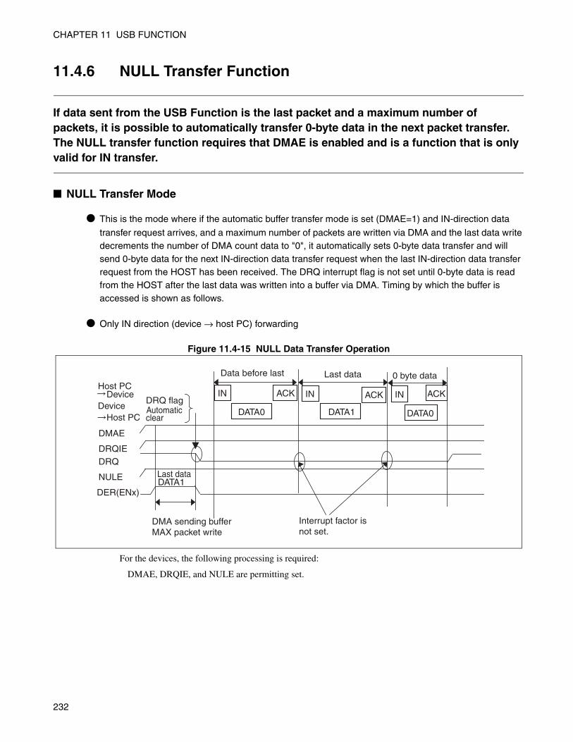
CHAPTER 11 USB FUNCTION
11.4.6 NULL Transfer Function
If data sent from the USB Function is the last packet and a maximum number of packets, it is possible to automatically transfer 0-byte data in the next packet transfer. The NULL transfer function requires that DMAE is enabled and is a function that is only valid for IN transfer.
NULL Transfer Mode
This is the mode where if the automatic buffer transfer mode is set (DMAE=1) and IN-direction data
transfer request arrives, and a maximum number of packets are written via DMA and the last data write decrements the number of DMA count data to "0", it automatically sets 0-byte data transfer and will send 0-byte data for the next IN-direction data transfer request when the last IN-direction data transfer request from the HOST has been received. The DRQ interrupt flag is not set until 0-byte data is read from the HOST after the last data was written into a buffer via DMA. Timing by which the buffer is accessed is shown as follows.
Only IN direction (device → host PC) forwarding
Figure 11.4-15 NULL Data Transfer Operation
For the devices, the following processing is required:
DMAE, DRQIE, and NULE are permitting set.
DRQ
0 byte data
NULE
DeviceHost PC
DMAE
DRQIE
ACK Device
DATA0
ACK
Last data
IN IN
DER(ENx)
DRQ flag
DMA sending bufferMAX packet write
DATA0
IN
DATA1
ACK
Data before last
DATA1Last data
Host PC
Automaticclear
Interrupt factor isnot set.
232
CHAPTER 12USB Mini-HOST
This chapter describes the functions and operation of USB Mini-HOST.
12.1 Feature of USB Mini-HOST
12.2 Diversity with USB HOST
12.3 Block Diagram of USB Mini-HOST
12.4 Register of USB Mini-HOST
12.5 Operation of USB Mini-HOST
12.6 Each Token Flow Chart of USB Mini-HOST
233

CHAPTER 12 USB Mini-HOST
12.1 Feature of USB Mini-HOST
USB Mini-HOST provides minimum host operations required and is a function that enables data to be transferred to and from Device without PC intervention.
Feature of USB Mini-HOSTUSB Mini-HOST has the following features.
• Automatic detection of Low Speed/Full Speed forwarding
• Low Speed/Full Speed forwarding support
• Automatic detection of connection and cutting device
• Reset sending function support to USB bus
• Support of IN/OUT/SETUP/SOF token
• Automatic transmission of handshake packet for IN token (excluding STALL)
• Handshake packet automatic detection at OUT token
• Supports a maximum packet length of 256 bytes.
• Various error (CRC error/toggle error/time-out) supports
• Wake Up function support
234

CHAPTER 12 USB Mini-HOST
12.2 Diversity with USB HOST
It indicates differences between the USB host and USB Mini-HOST.
Diversity with USB Host
Table 12.2-1 Diversity with USB Host
HOST Mini-HOST
Support Hub
Transfer Bulk transfer
Control transfer
Interrupt transfer
Isochronous transfer
Transfer speed Low Speed
Full Speed
PRE packet support
SOF packet support
Error CRC error
Toggle error
Time-out
Max. packet < Receive Data
Detection of connection and cutting of device
Transfer speed detection
: Supported: Not supported
235

CHAPTER 12 USB Mini-HOST
12.3 Block Diagram of USB Mini-HOST
Figure 12.3-1 shows the block diagram of USB Mini-HOST.
UART Block Diagram of USB Mini-HOST
Figure 12.3-1 Block Diagram of USB Mini-HOST
Explanation of blockCPUI/F BufferCPUI/FUSB bus reset control part RX control part TX control part:
Host TX control part:
TXRXTXENL HTX HRX HTXENL
: Explanation of block: Interface circuit block with CPU: Buffer and buffer control circuit block: Interface circuit block with CPU: USB bus reset and connection control block: Receive data serial to parallel conversion circuit and RX control circuit block: Transmission data parallel to serial conversion circuit and TX control circuit block for the USB Function: Transmission data parallel to serial conversion circuit and TX control circuit block for MiniHOST: Transmission data signal of function : Received data signal of function: Function transmission and receive direction signal: Mini-HOST transmit data signal: Mini-HOST receive data signal: Mini-HOST transmission and receive direction signal
RX
HRXSelector
TX
TXENL
HTX
HTXENL
CPU I/F
UDC I/F
BufferReceive
control unit
Transmitcontrol unit
Host receivecontrol unit
USB bus resetcontrol unit
236

CHAPTER 12 USB Mini-HOST
12.4 Register of USB Mini-HOST
In USB Mini-HOST, there are the following ten types of registers:• Host control register 0, 1(HCNT0/1) • Host interruption register (HIRQ) • Host error status register (HERR) • Host state status register (HSTATE) • SOF interruption FRAME comparison register (HFCOMP) • Retry timer setting register (HRTIMER) • HOST address register (HADR) • EOF setting register (HEOF) • FRAME setting register (HFRAME) • Host token end point register (HTOKEN)
Register of USB Mini-HOST
Continued
• Host control register 0
• Host control register 1
• Host interruption register
• Host error status register
7 6 5 4 3 2 1 0 ← bit number
Address: 0000C0H RWKIRE URIRE CMPIRE CNNIRE DIRE SOFIRE URST HOST HCNT0
Read/Write → (R/W) (R/W) (R/W) (R/W) (R/W) (R/W) (R/W) (R/W)
Initial value → (0) (0) (0) (0) (0) (0) (0) (0)
15 14 13 12 11 10 9 8 ← bit number
Address: 0000C1H Reserved Reserved Reserved Reserved Reserved SOFSTEP CANCEL RETRY HCNT1
Read/Write → (R/W) (R/W) (R/W) (R/W) (R/W) (R/W) (R/W) (R/W)
Initial value → (0) (0) (0) (0) (0) (0) (0) (1)
7 6 5 4 3 2 1 0 ← bit number
Address: 0000C2H TCAN Reserved RWKIRQ URIRQ CMPIRQ CNNIRQ DIRQ SOFIRQ HIRQ
Read/Write → (R/W) (R/W) (R/W) (R/W) (R/W) (R/W) (R/W) (R/W)
Initial value → (0) (0) (0) (0) (0) (0) (0) (0)
15 14 13 12 11 10 9 8 ← bit number
Address: 0000C3H LSTSOF RERR TOUT CRC TGERR STUFF HS HERR
Read/Write → (R/W) (R/W) (R/W) (R/W) (R/W) (R/W) (R/W)
Initial value → (0) (0) (0) (0) (0) (0) (11)
237

CHAPTER 12 USB Mini-HOST
Continued
Continued
• Host state status register
• SOF interruption FRAME comparison register
• Retry timer setting register
• Host address register
7 6 5 4 3 2 1 0 ← bit number
Address: 0000C4H Reserved ALIVE CLKSEL SOFBUSY SUSP TMODE CSTAT HSTATE
Read/Write → (-) (R/W) (R/W) (R/W) (R/W) (R) (R)
Initial value → (x) (0) (1) (0) (0) (1) (0)
15 14 13 12 11 10 9 8 ← bit number
Address: 0000C5H FRAMECOMP HFCOMP
Read/Write → (R/W)
Initial value → (00000000B)
7 6 5 4 3 2 1 0 ← bit number
Address: 0000C6H RTIMER0 HRTIMER
Read/Write → (R/W)
Initial value → (00000000B)
15 14 13 12 11 10 9 8 ← bit number
Address: 0000C7H RTIMER1 HRTIMER
Read/Write → (R/W)
Initial value → (00000000B)
7(23) 6(22) 5(21) 4(20) 3(19) 2(18) 1(17) 0(16) ← bit number
Address: 0000C8H Reserved RTIMER2 HRTIMER
Read/Write → (-) (R/W)
Initial value → (x) (00)
15 14 13 12 11 10 9 8 ← bit number
Address: 0000C9H Reserved Address HADR
Read/Write → (-) (R/W)
Initial value → (x) (0000000B)
238
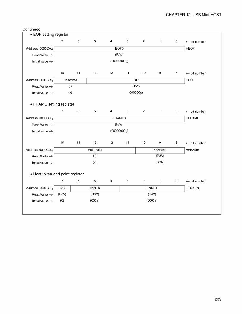
CHAPTER 12 USB Mini-HOST
Continued• EOF setting register
• FRAME setting register
• Host token end point register
7 6 5 4 3 2 1 0 ← bit number
Address: 0000CAH EOF0 HEOF
Read/Write → (R/W)
Initial value → (00000000B)
15 14 13 12 11 10 9 8 ← bit number
Address: 0000CBH Reserved EOF1 HEOF
Read/Write → (-) (R/W)
Initial value → (x) (000000B)
7 6 5 4 3 2 1 0 ← bit number
Address: 0000CCH FRAME0 HFRAME
Read/Write → (R/W)
Initial value → (00000000B)
15 14 13 12 11 10 9 8 ← bit number
Address: 0000CDH Reserved FRAME1 HFRAME
Read/Write → (-) (R/W)
Initial value → (x) (000B)
7 6 5 4 3 2 1 0 ← bit number
Address: 0000CEH TGGL TKNEN ENDPT HTOKEN
Read/Write → (R/W) (R/W) (R/W)
Initial value → (0) (000B) (0000B)
239

CHAPTER 12 USB Mini-HOST
12.4.1 Host Control Register 0, 1(HCNT0/HCNT1)
Host control registers 0, 1(HCNT0/HCNT1) specify the USB operation mode and the settings of an interrupt.
Host Control Register 0, 1(HCNT0/HCNT1)
Figure 12.4-1 Bit Configuration of Host Control Register 0, 1 (HCNT0/HCNT1)
[bit15 to bit11] Reserved
It is reserved bit.
Be sure to set this bit to "0".
[bit10] SOFSTEP: SOF interrupt condition selection
It sets whether an interrupt due to SOF is generated every time SOF is executed. The interrupt is
enabled when the SOFIRE bit in host control register 0 (HCNT0) is "1".
When it is "0", the interrupt is generated via the setting of the SOF interrupt FRAME comparison
register (HFCOMP), and when it is "1", the interrupt is unconditionally generated every time SOF is
executed. However, the interruption is not generated at the first SOF token. It is not initialized with the
RST bit in the UDC control register (UDCC).
Host control register 0
7 6 5 4 3 2 1 0 ← bit number
Address: 0000C0H RWKIRE URIRE CMPIRE CNNIRE DIRE SOFIRE URST HOST HCNT0
Read/Write → (R/W) (R/W) (R/W) (R/W) (R/W) (R/W) (R/W) (R/W)
Initial value → (0) (0) (0) (0) (0) (0) (0) (0)
Reset On/Off at UDCC RST bit→ ( ) ( ) ( ) ( ) ( ) ( ) () ( )
Host control register 1
15 14 13 12 11 10 9 8 ← bit number
Address: 0000C1H Reserved Reserved Reserved Reserved Reserved SOFSTEP CANCEL RETRY HCNT1
Read/Write → (R/W) (R/W) (R/W) (R/W) (R/W) (R/W) (R/W) (R/W)
Initial value → (0) (0) (0) (0) (0) (0) (0) (1)
Reset On/Off at UDCC RST bit → ( ) ( ) ( ) ( ) ( ) ( ) ( ) ( )
SOFSTEP Operation mode
0 Interrupt is generated due to the setting of HFCOMP.
1 Interruption generation
240

CHAPTER 12 USB Mini-HOST
[bit9] CANCEL: Token cancellation permission
This bit sets whether a token is to be cancelled when the token (which is issued in an EOF area) has
never been executed and is in waiting status if the SOFIRQ bit in the host interrupt register (HIRQ) is
"1". It is not initialized with the RST bit in the UDC control register (UDCC).
[bit8] RETRY: Retry permission
This bit sets whether a retry is attempted when a NAK and CRC errors happen. It is not initialized with
the RST bit in the UDC control register (UDCC).
[bit7] RWKIRE: Reactivation interrupt request permission
It is a bit to set whether an interrupt is to be generated when the Mini HOST function can be operational
after resume operation has been completed. In host mode, to enter suspend status, write "1" to the SUSP
bit in the host state status register. Only the host mode is effective. It is not initialized with the RST bit
in the UDC control register (UDCC).
[bit6] URIRE: USB bus reset interrupt request enable
This bit sets whether an interrupt is to be generated when reset operation to the USB bus has been
completed. Only the host mode is effective. It is not initialized with the RST bit in the UDC control
register (UDCC).
CANCEL Operation mode
0 Token continuance
1 Token discontinuance
RETRY Operation mode
0 No retry
1 Retry
RWKIRE Operation mode
0 Reactivation interrupt disable
1 Reactivation interrupt enable
URIRE Operation mode
0 Interrupt disabled after USB bus is reset
1 Interruption enable after USB bus is reset
241

CHAPTER 12 USB Mini-HOST
[bit5] CMPIRE: Completion interrupt request enable
It sets whether an interrupt is generated when a token has been completed. Only the host mode is
effective. It is not initialized with the RST bit in the UDC control register (UDCC).
[bit4] CNNIRE: Connection interrupt request enable
It is a bit used to set whether an interrupt is generated when a connection is made to a device. Only the
host mode is effective. It is not initialized with the RST bit in the UDC control register (UDCC).
[bit3] DIRE: Disconnection interrupt request enable
It is a bit used to set whether an interrupt is generated when a disconnection is made to a device. Only
the host mode is effective. It is not initialized with the RST bit in the UDC control register (UDCC).
[bit2] SOFIRE:SOF interrupt request enable
It is a bit used to set whether an interrupt is generated when sending an SOF. Only the host mode is
effective. It is not initialized with the RST bit in the UDC control register (UDCC).
CMPIRE Operation mode
0 Completion interrupt disabled
1 Completion interrupt enabled
CNNIRE Operation mode
0 Interrupt disabled when device is connected
1 Interruption enable when device is connected
DIRE Operation mode
0 Interrupt disabled when device is cut
1 Interruption enable when device is cut
SOFIRE Operation mode
0 Interrupt disabled when SOF is transmitted
1 Interrupt enabled when SOF is transmitted
242
CHAPTER 12 USB Mini-HOST
[bit1] URST: USB bus reset
It is set to USB bus whether reset is generated. It indicates "1" while the USB bus is being reset and
turns "0" when it has been completed. It is forbidden to set it to "1" when the SUSP bit in the host state
status register (HSTATE) is "1" or while a token is being executed. It is also forbidden to update the
host control registers (HCNT0, HCNT1) while it is set to "1". Only the host mode is effective. To
update them, you must set the RST bit in the UDC control register (UDCC) to "0".
[bit0] HOST: Host mode
The LSI is set whether it is a function or Mini-HOST. Since it is not initialized due to the RST bit in the
UDC control register (UDCC), change it when the RST bit is "1".
And, if you change the mode from function mode to host mode, make a disconnection to the HOST PC
or HUB by setting the HCON bit in the UDC control register (UDCC) to "1". If you change the mode
from host mode to function mode, ensure that the SOFBUSY bit in the host status register (HSTATE) is
set to "0" and the TKNEN bit in the host token endpoint register (HTOKEN) is "000B".
URST Operation mode
0 USB bus state maintenance
1 USB bus reset
HOST Operation mode
0 Function mode
1 Host mode
243

CHAPTER 12 USB Mini-HOST
12.4.2 Host Interruption Register (HIRQ)
The host interrupt register (HIRQ) indicates for the interrupt request flag for USB Mini- HOST. It can allow an interrupt to be generated by setting the interrupt enable bit in the host control registers (HCNT0/1) except the TCAN bit.
Host Interruption Register (HIRQ)
Figure 12.4-2 Bit Configuration of Host Interruption Register (HIRQ)
[bit7] TCAN: Token cancellation flag
When the SOFIRQ bit in the host interrupt register (HIRQ) becomes "1", it indicates that a token is
cancelled without being executed once. Any interrupt is not raised because the register is combined with
interrupt due to SOF. To set it to "0", write "0" to it.
To update them, you must set the RST bit in the UDC control register (UDCC) to "0".
[bit6] Reserved
It is reserved bit.
Be sure to set this bit to "0".
[bit5] RWKIRQ: Reactivation interrupt request
It indicates that resume operation has been completed. When it becomes "1", it gets back to "0" by
writing "0" to it. When you write "1" to it, the current state will be preserved. If the RWKIRE bit in the
host control register 0 (HCNT0) is "1", an interrupt is generated when it is "1". The interrupt signal is
cleared when it is cleared with "0".
To update them, you must set the RST bit in the UDC control register (UDCC) to "0".
Host interruption register
7 6 5 4 3 2 1 0 ← bit number
Address: 0000C2H TCAN Reserved RWKIRQ URIRQ CMPIRQ CNNIRQ DIRQ SOFIRQ HIRQ
Read/Write → (R/W) (R/W) (R/W) (R/W) (R/W) (R/W) (R/W) (R/W)
Initial value → (0) (0) (0) (0) (0) (0) (0) (0)
Reset On/Off at UDCC RST bit → () () () () () ( ) ( ) ()
TCAN Operation mode
0 There is no token discontinuance.
1 There is token discontinuance.
RWKIRQ Operation mode
0 There is no interrupt request by reactivation.
1 There is an interrupt request by reactivation.
244

CHAPTER 12 USB Mini-HOST
[bit4] URIRQ: USB bus interrupt request
It is shown that reset in USB bus ended. When it becomes "1", it gets back to "0" by writing "0" to it.
When you write "1" to it, the current state will be preserved. If the URIRE bit in the host control
register 0 (HCNT0) is "1", an interrupt is generated when it is "1". The interrupt signal is cleared when
it is cleared with "0".
To update them, you must set the RST bit in the UDC control register (UDCC) to "0".
[bit3] CMPIRQ: Completion interrupt request
It is shown to have completed the token. It is not set to "1" when the TCAN bit in the host interrupt
register (HIRQ) is "1". When it becomes "1", it gets back to "0" by writing "0" to it. When you write
"1" to it, the current state will be preserved. If the CMPIRE bit in the host control register 0 (HCNT0) is
"1", an interrupt is generated when it is "1". The interrupt signal is cleared when it is cleared with "0".
To update them, you must set the RST bit in the UDC control register (UDCC) to "0".
[bit2] CNNIRQ: Connected interrupt request
It is shown to have detected the connection of the device. When it becomes "1", it gets back to "0" by
writing "0" to it. When you write "1" to it, the current state will be preserved. If the CNNIRE bit in the
host control register 0 (HCNT0) is "1", an interrupt is generated when it is "1". The interrupt signal is
cleared when it is cleared with "0".
It is not initialized with the RST bit in the UDC control register (UDCC).
URIRQ Operation mode
0 There is no interrupt request by USB bus reset.
1 There is an interrupt request by USB bus reset.
CMPIRQ Operation mode
0 There is no interrupt request by token completion.
1 There is an interrupt request by the token completion.
CNNIRQ Operation mode
0 Indicates interrupt request due to device connection detected.
1 Interrupt request none by device connection detection.
245

CHAPTER 12 USB Mini-HOST
[bit1] DIRQ: Cutting interrupt request
It is shown to have detected cutting the device. When it becomes "1", it gets back to "0" by writing "0"
to it. When you write "1" to it, the current state will be preserved. If the DIRE bit in the host control
register 0 (HCNT0) is "1", an interrupt is generated when it is "1". The interrupt signal is cleared when
it is cleared with "0".
It is not initialized with the RST bit in the UDC control register (UDCC).
[bit0] SOFIRQ: SOF interruption requests
Whether the SOF token was begun is shown. When it becomes "1", it gets back to "0" by writing "0" to
it. When you write "1" to it, the current state will be preserved. If the SOFIRE bit in the host control
register 0 (HCNT0) is "1", an interrupt is generated when it is "1". The interrupt signal is cleared when
it is cleared with "0".
To update them, you must set the RST bit in the UDC control register (UDCC) to "0".
DIRQ Operation mode
0 There is interrupt request by device cutting detection.
1 There is no interrupt request by device cutting detection.
SOFIRQ Operation mode
0 There is no interrupt request by SOF token beginning.
1 There is an interrupt request by the SOF token beginning.
246

CHAPTER 12 USB Mini-HOST
12.4.3 Host Error Status Register (HERR)
The host error status register (HERR) is a register that indicates whether an error occurs or not when sending or receiving data in host mode.
Host Error Status Register (HERR)
Figure 12.4-3 Bit Configuration of Host Error Status Register (HERR)
[bit15] LSTSOF:SOF execution error
It indicates that an SOF token could not be executed because another token was running when you tried
to execute it in host mode. Please do "0" in the writing to clear "1". To update them, you must set the
RST bit in the UDC control register (UDCC) to "0".
[bit14] RERR: Receive error
It indicates whether data more than a maximum number of packets set was received in host mode.
When the reception error occurs, TOUT is set in "1".
Please do "0" in the writing to clear "1". To update them, you must set the RST bit in the UDC control
register (UDCC) to "0".
Host error status register
15 14 13 12 11 10 9 8 ← bit number
Address: 0000C3H LSTSOF RERR TOUT CRC TGERR STUFF HS HERR
Read/Write → (R/W) (R/W) (R/W) (R/W) (R/W) (R/W) (R/W)
Initial value → (0) (0) (0) (0) (0) (0) (11)
Reset On/Off at UDCC RST bit → () () () () () () ()
LSTSOF Operation mode
0 SOF execution
1 SOF execution error
RERR Operation mode
0 No receive error
1 The maximum packet reception error
247

CHAPTER 12 USB Mini-HOST
[bit13] TOUT: Time-out
It indicates whether time-out was generated. If "1" is cleared, write "0" to this bit. The bit is updated
after the RST bit of the UDC control register (UDCC) is set to "0".
[bit12] CRC:CRC error
It is shown whether the CRC error occurred at the host mode. When the CRC error occurs, TOUT is set
in "1".
Please do "0" in the writing to clear "1".
To update them, you must set the RST bit in the UDC control register (UDCC) to "0".
[bit11] TGERR: Toggle error
In indicates whether an toggle error occurs in host mode. Please do "0" in the writing to clear "1". To
update them, you must set the RST bit in the UDC control register (UDCC) to "0".
[bit10] STUFF: Stuffing error
It indicates whether a stuffing error happens in host mode. TOUT is also set to "1" when a stuffing error
occurs.
Please do "0" in the writing to clear "1". To update it, you must set the RST bit in the UDC control
register (UDCC) to "0".
TOUT Operation mode
0 There is no time-out.
1 There is a time-out.
CRC Operation mode
0 There is no CRC error.
1 There is a CRC error.
TGERR Operation mode
0 There is no toggle error.
1 There is a toggle error.
248

CHAPTER 12 USB Mini-HOST
[bit9, bit8] HS: Handshake status
It indicates the status of handshake operations between transmission and reception in host mode. It
indicates NULL when handshake operation is not performed due to any reasons such as an error and the
SOF token is completed. It is updated when transmission or reception has been completed. To update
them, you must set the RST bit in the UDC control register (UDCC) to "0".
Table 12.4-1 Handshake
bit9 bit8 Handshake
0 0 ACK
0 1 NAK
1 0 STALL
1 1 NULL
249

CHAPTER 12 USB Mini-HOST
12.4.4 Host State Status Register (HSTATE)
The host state status register (HSTATE) is a register that indicates the status of the USB circuit such as connections to devices and transfer mode. Note that the CLKSEL bit is also enabled in the function mode.
Host State Status Register (HSTATE)
Figure 12.4-4 Bit Configuration of Host State Status Register (HSTATE)
[bit7, bit6] Reserved
It is reserved bits. The reading is irregular. The writing does not influence the operation.
[bit5] ALIVE: Keep-Alive function setting
It is a bit that sets the Keep-Alive function in Low Speed. If you set it to "1" when the CLKSEL bit in
the host state status register (HSTATE) is "0", SE0 is will be output instead of an SOF. If it is enabled
when the CLKSEL bit in the host state status register (HSTATE) is "0", and the CLKSEL becomes "1",
an SOF will be output regardless of the setting of the ALIVE bit.
[bit4] CLKSEL: Clock selection
The operation clock of USB is selected. You must set it to "1" for Full Speed, and to "0" for Low
Speed.
You must switch clock when the RST bit in the UDC control register (UDCC) is "1" and both the
function mode and host mode are enabled. "0" setting at the function mode is a interdiction.
Host state status register
7 6 5 4 3 2 1 0 ← bit number
Address: 0000C4H Reserved Reserved ALIVE CLKSEL SOFBUSY SUSP TMODE CSTAT HSTATE
Read/Write → (-) (-) (R/W) (R/W) (R/W) (R/W) (R) (R)
Initial value → (x) (x) (0) (1) (0) (0) (1) (0)
Reset On/Off at UDCC RST bit → (-) (-) ( ) ( ) () () ( ) ( )
ALIVE Operation mode
0 SOF
1 SE0 output (Keep-Alive)
CLKSEL Operation mode
0 Clock for Low Speed
1 Clock for Full Speed
250

CHAPTER 12 USB Mini-HOST
[bit3] SOFBUSY:SOF timer operation
It indicates whether the SOF timer is operating in host mode. Sending SOF stops when "0" is done in
the writing. To update them, you must set the RST bit in the UDC control register (UDCC) to "0".
[bit2] SUSP: Suspend
It is a bit used to set suspend status in host mode. Writing "1" to the bit enables suspend status. When
you write "0" to the bit that holds "1" or the USB bus changes to k-state status, the suspend status is
deselected, the RWKIRQ bit in the host interrupt register (HIRQ) is "1". When connection or
disconnection is detected if the SUSP bit is "1", you must write "0" to the bit. Then, when disconnection
or connection is detected and the SUSP bit is cleared, the RWKIRQ bit in the host interrupt register
(HIRQ) is set to "1" twice, and overwrite the RWKIRQ bit with "1" when it is set to "1". It is forbidden
to set the bit to "1" while the USB is operating (such as resetting the USB bus or sending/receiving
data).
In host mode, it is forbidden to stop the USB clock even in suspend status. To update it, you must set
the RST bit in the UDC control register (UDCC) to "0" and are prohibited to set it to "1" in function
mode. In addition, if it is "1" when you change the mode from host mode to function mode, you must
get out of suspend status by writing "0" into it before changing the mode.
[bit1] TMODE: Transfer mode
The transfer mode at the host mode is shown. Write "1" for the write operation. It is not initialized with
the RST bit in the UDC control register (UDCC). Please use the CPU clock at 24 MHz.
SOFBUSY Operation mode
0 SOF timer is stop.
1 SOF timer is working.
Table 12.4-2 Suspend Setting
SUSP Operation
"1" Write Suspend
They are "0" writing at "1" state. Resume
The others State maintenance
TMODE Operation mode
0 Low Speed
1 Full Speed
251

CHAPTER 12 USB Mini-HOST
[bit0] CSTAT: Connected state
It is whether the device is connected is shown. The terminal for Mini HOST becomes an object. It is not
initialized with the RST bit in the UDC control register (UDCC).
CSTAT Operation mode
0 Device cut off
1 Device connect
252

CHAPTER 12 USB Mini-HOST
12.4.5 SOF Interruption FRAME Comparison Register (HFCOMP)
The SOF interrupt FRAME comparison register (HFCOMP) is a register used to set data that is compared with the lower 8 bits of FRAME Number for SOF token. If the lower 8 bits of FRAME Number is compared with the HFCOMP register and a match is detected with the SOFIRE bit in host control register 0 (HCNT0) set to "1", an interrupt will be generated by setting the SOFIRQ bit in the host interrupt register (HIRQ) to "1" when starting SOF transmission.
SOF Interruption FRAME Comparison Register (HFCOMP)
Figure 12.4-5 Bit Configuration of SOF Interruption FRAME Comparison Register (HFCOMP)
[bit15 to bit8] FRAMECOMP
It sets data that is to be compared with the lower 8 bits of Frame Number. It is not initialized with the
RST bit in the UDC control register (UDCC). To update them, you must set the RST bit in the UDC
control register (UDCC) to "0".
SOF interruption FRAME comparison register
15 14 13 12 11 10 9 8 ← bit number
Address: 0000C5H FRAMECOMP HFCOMP
Read/Write → (R/W)
Initial value → (00000000B)
Reset On/Off at UDCC RST bit → ( )
253

CHAPTER 12 USB Mini-HOST
12.4.6 Retry Timer Setting Register (HRTIMER)
The retry timer setting register (HRTIMER) is a register used to set a retry time period for a token.
Retry Timer Setting Register (HRTIMER)
Figure 12.4-6 Bit Configuration of Retry Timer Setting Register (HRTIMER)
[bit23 to bit18] Reserved
There are reserved bits.
The reading is irregular. The writing does not influence the operation.
[bit17 to bit0] RTIMER0, RTIMER1, RTIMER2
These bits set a time to retry a token. When the RETRY bit of the host control register (HCNT1) is "1",
a retry timer is activated after the token is started, and the timer is decremented by "1" due to 1-bit
transfer clock (12 MHz at Full Speed). When the retry timer becomes "0", token retry dose not execute.
When the token retry occurs in an EOF area, the retry timer stops until the SOF is completed. The timer
value that was stopped is decremented by 1 after the SOF is executed. It is not initialized with the RST
bit in the UDC control register (UDCC). To update them, you must set the RST bit in the UDC control
register (UDCC) to "0".
Retry timer setting register
7 6 5 4 3 2 1 0 ← bit number
Address: 0000C6H RTIMER0 HRTIMER
Read/Write → (R/W)
Initial value → (00000000B)
Reset On/Off at UDCC RST bit → ( )
15 14 13 12 11 10 9 8 ← bit number
Address: 0000C7H RTIMER1 HRTIMER
Read/Write → (R/W)
Initial value → (00000000B)
Reset On/Off at UDCC RST bit → ( )
7(23) 6(22) 5(21) 4(20) 3(19) 2(18) 1(17) 0(16) ← bit number
Address: 0000C8H Reserved RTIMER2 HRTIMER
Read/Write → (-) (R/W)
Initial value → (x) (00)
Reset On/Off at UDCC RST bit → (-) ( )
254

CHAPTER 12 USB Mini-HOST
12.4.7 Host Address Register (HADR)
The host address register (HADR) is a register used for an address field when a token is sent.
Host Address Register (HADR)
Figure 12.4-7 Bit Configuration of Host Address Register (HADR)
[bit15] Reserved
It is reserved bit. The reading is irregular. The writing does not influence the operation.
[bit14 to bit8] Address: Address
The address of the token is set. It is not initialized with the RST bit in the UDC control register
(UDCC). To update them, you must set the RST bit in the UDC control register (UDCC) to "0".
Host address register
15 14 13 12 11 10 9 8 ← bit number
Address: 0000C9H Reserved Address HADR
Read/Write → (-) (R/W)
Initial value → (x) (0000000B)
Reset On/Off at UDCC RST bit → (-) ( )
255

CHAPTER 12 USB Mini-HOST
12.4.8 EOF Setting Register (HEOF)
The EOF setting register (HEOF) is a register that sets a time period for which a token is inhibited before the execution of the SOF token. If the data of the SOF timer turns out to be lower than data in the HEOF register as a result of comparing both, and any of an IN token, OUT token, and SETUP token execution requests is made, it will be run after the SOF token is executed. This prevents an SOF token generated by hardware and other tokens from being simultaneously executed. The unit of time for the HEOF register is one-bit transfer time.
EOF Setting Register (HEOF)
Figure 12.4-8 Bit Configuration of EOF Setting Register (HEOF)
[bit15, bit14] Reserved
There are reserved bits. The reading is irregular. The writing does not influence the operation.
[bit13 to bit0] EOF1,EOF0:EOF
Set a time period during which the execution of a token is inhibited before the execution of SOF. Set a
margin that is longer than one packet length. The unit is one bit forwarding time. It is not initialized
with the RST bit in the UDC control register (UDCC). To update them, you must set the RST bit in the
UDC control register (UDCC) to "0".
For the MAXPKT=64 byte and Full Speed of set example
(Token_length + packet_length + header + CRC)×7/6 + Turn_around_time
=(34 bit + 546 bit)×7/6 + 36 bit = 712.7 bits
As the above is true, specify (2C9)H.
EOF setting register
7 6 5 4 3 2 1 0 ← bit number
Address: 0000CAH EOF0 HEOF
Read/Write → (R/W)
Initial value → (00000000B)
Reset On/Off at UDCC RST bit → ( )
15 14 13 12 11 10 9 8 ← bit number
Address: 0000CBH Reserved EOF1 HEOF
Read/Write → (-) (R/W)
Initial value → (x) (000000B)
Reset On/Off at UDCC RST bit → (-) ( )
256
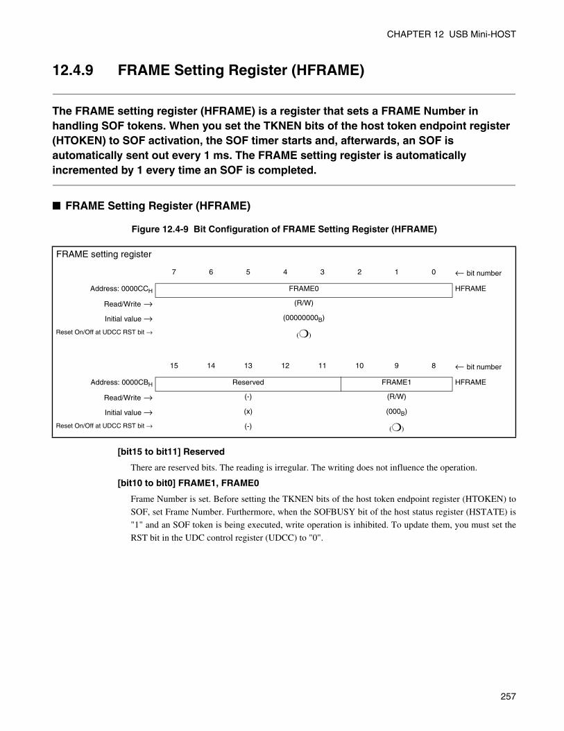
CHAPTER 12 USB Mini-HOST
12.4.9 FRAME Setting Register (HFRAME)
The FRAME setting register (HFRAME) is a register that sets a FRAME Number in handling SOF tokens. When you set the TKNEN bits of the host token endpoint register (HTOKEN) to SOF activation, the SOF timer starts and, afterwards, an SOF is automatically sent out every 1 ms. The FRAME setting register is automatically incremented by 1 every time an SOF is completed.
FRAME Setting Register (HFRAME)
Figure 12.4-9 Bit Configuration of FRAME Setting Register (HFRAME)
[bit15 to bit11] Reserved
There are reserved bits. The reading is irregular. The writing does not influence the operation.
[bit10 to bit0] FRAME1, FRAME0
Frame Number is set. Before setting the TKNEN bits of the host token endpoint register (HTOKEN) to
SOF, set Frame Number. Furthermore, when the SOFBUSY bit of the host status register (HSTATE) is
"1" and an SOF token is being executed, write operation is inhibited. To update them, you must set the
RST bit in the UDC control register (UDCC) to "0".
FRAME setting register
7 6 5 4 3 2 1 0 ← bit number
Address: 0000CCH FRAME0 HFRAME
Read/Write → (R/W)
Initial value → (00000000B)
Reset On/Off at UDCC RST bit → ()
15 14 13 12 11 10 9 8 ← bit number
Address: 0000CBH Reserved FRAME1 HFRAME
Read/Write → (-) (R/W)
Initial value → (x) (000B)
Reset On/Off at UDCC RST bit → (-) ()
257

CHAPTER 12 USB Mini-HOST
12.4.10 Host Token Endpoint Register (HTOKEN)
The host token endpoint register (HTOKEN) is a register that sets a toggle, endpoint, and token.
Host Token Endpoint Register (HTOKEN)
Figure 12.4-10 Bit Configuration of Host Token Endpoint Register (HTOKEN)
[bit7] TGGL: Toggle
This bit sets toggle data. At transmission, the toggle data is sent according to the bit. At reception, the
received toggle data is compared to the toggle data which the bit shows and use at the error detection.
The bit is updated after the RST bit of the UDC control register (UDCC) is set to "0" and the TKNEN
bit to (0, 0, 0).
[bit6 to bit4] TKNEN: Token permission
These bits send a token corresponding to the setting. After the operation is completed (bit6, bit5, bit4) =
(0, 0, 0), the CMPIRQ bit of the host interrupt register (HIRQ) is set to "1". At that time, if the CMPIRE
bit of the host control register 0 (HCNT0) is "1", an interrupt generates.
The TGGL and ENDPT bits are ignored during the SOF token. To write to the TKNEN bits, you must
set the RST bit in the UDC control register (UDCC) to "0" and turn the mode to host mode. In addition,
if you issue a token again because an interrupt due to a token is generated, you must wait three cycles or
longer in terms of USB transfer clock (12 MHz for Full Speed and 1.5 MHz for Low Speed) before
writing to the TKNEN bits. Note that writing to the TKNEN bits will not run a token in disconnection
status (HSTATE CSTAT= 0).
Host token end point register
7 6 5 4 3 2 1 0 ← bit number
Address: 0000CEH TGGL TKNEN ENDPT HTOKEN
Read/Write → (R/W) (R/W) (R/W)
Initial value → (0) (000B) (0000B)
Reset On/Off at UDCC RST bit → () () ()
TGGL Operation Mode
0 Data 0
1 Data 1
258

CHAPTER 12 USB Mini-HOST
Note:
The PRE packet is not supported.
When the SOFBUSY bit in the host state status register (HSTATE) is "1", setting bit6, bit5, and bit4to "1", "0", and "0", respectively, is forbidden.
[bit3 to bit0] ENDPT: end point
The transmitted and received endpoint to the device is set. To update them, you must set the RST bit in
the UDC control register (UDCC) to "0".
Table 12.4-3 Token Setting
bit6 bit5 bit4 Operation
0 0 0 No send out
0 0 1 SETUP is sent
0 1 0 IN is sent.
0 1 1 OUT is sent.
1 0 0 SOF is sent.
259

CHAPTER 12 USB Mini-HOST
12.5 Operation of USB Mini-HOST
The operation of USB Mini-HOST is explained.
Connection of device
The software detects that the external USB device was connected.
Reset of USB bus
USB bus is reset.
Token packet
Three kinds of tokens can be selected at the host mode.
Data packet
The data packet is transmitted and received.
Handshake packet
It informs send/receive partners of status via handshake packet.
Retry function
When an error etc. occur at the packet termination, the retry operation is continued.
SOF INTERRUPT
The interruption is generated.
Error status
Various errors are displayed.
Packet end
When the packet ends, the interruption is generated.
Suspend-resume
It puts the USB circuit in suspend-resume status.
Cutting of device
The detection of the status of Mini-HOST pins determines the disconnection.
260

CHAPTER 12 USB Mini-HOST
12.5.1 Connection of Device
The method for detecting the connection of the external USB device by software is described.
Setting of Mini-HOST FunctionTo make it operate as a host of the USB device, set the HOST bit of the host control register 0 (HCNT0) to
"1".
Disconnection Status, Connection Status of the External USB DeviceWhen the external USB device is disconnected, both Mini-HOST pins, D + and D-, are "L" by the pull-
down resistor. Then, the CSTAT bit in the host state status register (HSTATE) is "0", and the TMODE bit
is indefinite. The CSTAT bit of the host state status register (HSTATE) becomes "1" when the external
USB device is connected.
Connected Detection of External USB DeviceTo detect the connection of the external USB device, set the CNNIRE bit of the host control register 0
(HCNT0) to "1". The CNNIRQ bit of the host interrupt register (HIRQ) becomes "1", and a device
connection interrupt is generated. To clear this interrupt, write "0" to the CNNIRQ bit of the host interrupt
register (HIRQ). To detect the connection of the external USB device not through interrupt but through
polling, create a program so that it ensures that the CNNIRE bit of the host control register 0 (HCNT0) is
set to "0" and the CNNIRQ bit of the host interrupt register (HIRQ) is "1".
Acquiring Transfer Speed of Destination USB Device and Selecting ClockTo acquire the transfer speed of a destination USB after detecting the connection, make reference to the
value of the TMODE of the host state status register (HSTATE). The relation between the transfer speed
and the TMODE bit of the host state status register (HSTATE) is as follows:
• When a destination device is a Full Speed-enabled device → TMODE= 1
• When a destination device is a Low Speed-enabled device → TMODE= 0
After the transfer speed of the external USB device is acquired, when the RST bit of the UDC control
register (UDCC) is "1", update the CLKSEL bit of the host state status register (HSTATE) based on the
acquired transfer speed. The relation between the TMODE and CLKSEL bits of the host status register
(HSTATE) is as follows:
• TMODE = 1 → "1" is set to CLKSEL bit.
• TMODE = 0 → "0" is set to CLKSEL bit.
261

CHAPTER 12 USB Mini-HOST
Figure 12.5-1 Connecting Detection Timing Example of Speed Device (HCNT0 Bit0 = 0)
Note:
The CSTAT bit of the host state status register (HSTATE) becomes "1" in 2.5µs after the connectionof the external USB device.
The TMODE and CSTAT bits of the host state status register (HSTATE) are updated regardless ofthe setting of the HOST bit in the host control register 0 (HCNT0).
LIN device connection
Indeterminate
"0"
Terminal D+ for Mini-HOST
Terminal D- for Mini-HOST
CSTAT bit of HSTATE
TMODE bit of HSTATE
CNNIRQ of HIRQ bit
HOST bit of HCNT
2.5ms
262

CHAPTER 12 USB Mini-HOST
12.5.2 Reset of USB Bus
When you set the URST bit of the host control register 0 (HCNT0) to "1" in the host mode, it sends out SE0 for not less than 10 ms and resets the USB bus. When the USB bus has been reset, it sets back the URST bit of the host control register to "0" and generates an interrupt and the URIRQ bit of the host interrupt register (HIRQ) is set to "1" when the URIRE bit of the host control register 0 (HCNT0) is "1." If you clear the interrupt, write "0" to the URIRQ bit of the host interrupt register (HIRQ).
Notes before and after Reset of USB BusPlease note the following points about reset of USB bus.
1. Before the USB bus is reset, confirm that the device is connected to and the CSTAT bit of the host state
status register (HSTATE) is set to "1".
2. When you reset the USB bus, the CSTAT bit of the host state status register (HSTATE) turns to "0" and
the USB device is put into disconnection status. Then, the DIRQ bit of the host interrupt control register
(HIRQ) does not become "1".
3. After the USB bus is reset, you must update the CLKSEL bit of the host state status register (HSTATE)
to match the TMODE bit of the same register if you compare them and they do not match. Before you
update the CLKSEL bit, ensure that the RST bit of the UDC control register (UDCC) is "1".
Figure 12.5-2 Reset Timing Example to Device
Terminal D+ for Mini-HOST
Terminal D- for Mini-HOST
URST bit of HCNT
CSTAT bit of HSTATE
URIRQ bit of HIRQ(HCNT URIRE=1)
10µs
2.5µsWrite "1" to HCNT URST bit
263

CHAPTER 12 USB Mini-HOST
12.5.3 Token Packet
If you execute any of an IN token, OUT token, and SETUP token in the host mode, a token packet is started when you set necessary data in the host token register (HTOKEN) after you set the PKS bit of the EP1 control register (EP1C) or EP2 control register (EP2C) based on the host address register (HADR) and the DIR bit in EP1C. In handling an SOF token, you must set necessary data in the host token register (HTOKEN) after configuring the FRAME setting register (HFRAME) and EOF setting register (HEOF). If registers (HADR, EP1C, EP2C, HFRAME, and HEOF) have not been changed, setting them is not required.
Setting of Token PacketFor the IN token, OUT token, and SETUP token, set the destination address to the host address register
(HADR), and set the maximum bytes of one packet to the PKS bit of the EP1 control register (EP1C) or the
EP2 control register based on the token to be executed and the DIR bit of the EP1 control register.
If the DIR bit of the EP1 control register (EP1C) is "1", the buffer for endpoint 1 is used as an OUT-
direction buffer and the one for endpoint 2 is used as an IN- direction buffer. Then, set the DIR bit of the
EP2 control register (EP2C) to "0".
If the DIR bit of the EP1 control register (EP1C) is "0", the buffer for endpoint 1 is used as an IN- direction
buffer and the one for endpoint 2 is used as an OUT- direction buffer. Then, set the DIR bit of the EP2
control register (EP2C) to "1".
If you want to use the buffer for endpoint 1, you must ensure that the DRQ bit of EP1 status register (EP1S)
is set to "1" and if you want to use the buffer for endpoint 2, you must ensure that the DRQ bit of EP2
status register (EP2S) is set to "1," before setting the target endpoint, token, and toggle data in the host
token endpoint register (HTOKEN). The USB circuit sends out a token packet in the order of a Sync, token,
address, endpoint, CRC5, and EOP based on the specified token (a Sync, CRC5, and EOP are automatically
sent). After one packet is ended, the CMPIRQ bit of the host interrupt register (HIRQ) becomes "1", and
the TKNEN bit of the host token endpoint register (HTOKEN) is set to (000B) (See "12.5.7 SOF
Interrupt"). At that time, if the CMPIRE bit of the host control register 0 (HCNT0) is "1", an interrupt
occurs. To clear the interrupt, write "0" to the CMPIRQ bit of the host interrupt register (HIRQ).
Figure 12.5-3 Example of Register Setting until Execution of IN/OUT/SETUP Token
Write to EP1C or EP2C
Write to HTOKEN
Write to HADR(when a change is required)(when a change is required)
Register write signal
Confirm the status of the buffer for endpoint 1/endpoint 2
264

CHAPTER 12 USB Mini-HOST
In the case of an SOF token, when you set an EOF time and FRAME number in the EOF setting register
(HEOF) and FRAME setting register (HFRAME), and write the code of the SOF token to the TKNEN bits
of the host token endpoint register (HTOKEN), a Sync, SOF token, FRAME number, CRC5, and EOP will
be sent out and the SOFBUSY bit of the host state status register (HSTATE) is set to "1" and HFRAME is
incremented by 1. In this case, the CMPIRQ of the host interrupt register (HIRQ) is also set to "1", and the
TKNEN bit of the host token endpoint register (HTOKEN) is cleared to (000)B. When the CMPIRE bit of
host control register 0 (HCNT0) is "1", an interrupt occurs. Then, when the SOF that generates
automatically is used, the interrupt by the CMPIRQ does not occur. To clear the interrupt of the token
completion, write "0" to the CMPIRQ of the HIRQ.
SOF is automatically sent out every 1 ms while the SOFBUSY bit of the host state status register
(HSTATE) is "1". The conditions (SOF stop conditions) that make the SOFBUSY bit of the host state
status register (HSTATE) "0" are as follows:
• "0" write to SOFBUSY bit of host state register (HSTATE)
• Reset ("1" write to URST bit of HCNT) in USB bus
• "1" write to SUSP bit of host state status register (HSTATE)
• Cutting of the device (For "0" the CSTAT bit of HSTATE).
To switch from host mode to function mode, first, ensure that the SOFBUSY bit of the host state status
register (HSTATE) is "0" after writing "0" to it.
If you want to set back the SOFBUSY bit of the host state status register (HSTATE) to "1" again, you need
to run an SOF token once again.
To prevent the simultaneous executions of an SOF token and other tokens, the EOF setting register is used
to run a token you have set after making it wait for the end of SOF execution if you write to the TKNEN
bits of the host token endpoint register (HTOKEN) in a time period from the EOF setting time to SOF start
time. The unit of time for the EOF setting register is one-bit time. For example, when setting (10H) to the
EOF setting register, the following time is required: 16×1/22 MHz = 13333.3 ns in Full speed mode and
16×1/1.5 MHz = 10666.6 ns in Low speed mode. If the EOF set time is shorter than one packet time, the
SOF execution max overlap other token execution. In this case, the LSTOF bit of host error status register
(HERR) is set to "1", the SOF is not executed. When the LSTOF bit of the host error status register
(HERR) is set to "1", you must increase data of the EOF setting register. (See "12.4.8 EOF Setting Register
(HEOF)")
Figure 12.5-4 SOF Timing
EOF set time
SOF start
EOF set time
EOF >1 packet time
SOF start
1ms
265

CHAPTER 12 USB Mini-HOST
12.5.4 Data Packet
If a data packet is transmitted after a token packet has been sent, toggle data will be transmitted based on the TGGL bit of the host token endpoint register (HTOKEN), and the buffer data for endpoint 1 or endpoint 2 according to the DIR bit of the EP1 control register (EP1C), CRC16 data, and EOP is sent. In the case of receiving a data packet, the TGGL bit of the host token endpoint register (HTOKEN) and received toggle data are compared, and, if they match, the received data is written to the buffer for endpoint 1 or endpoint 2 based on the DIR bit of the EP1 control register (EP1C) and the CRC16 is checked for an error.
Data PacketAfter sending a token packet, the data packet is executed in the following procedure:
At Transmission
• Automatic sending of Sync
• DATA0 is transmitted when the TGGL bit of the host token endpoint register (HTOKEN) is "0" andDATA1 is transmitted when the TGGL bit is "1".
• The buffer for endpoint 1 is selected when the DIR bit of the EP1 control register (EP1C) is "1" andotherwise the one for endpoint 2 is selected when the DIR bit is "0" and all transmit data is sent.
• The CRC16-bit is sent.
• The EOP 2-bit is sent.
• The J State 1-bit is sent.
At Reception
• Reception of Sync
• The toggle data is received, and is compared with the TGGL bit of the host token endpoint register(HTOKEN).
• If they match as a result of the comparison, the buffer for endpoint 2 is selected when the DIR bit of theEP1 control register (EP1C) is "1" and the one for endpoint 0 is selected when the DIR bit is "0" and thereceived data is written into it.
• When the EOF is received, the CRC16 bit is inspected.
You must set inversion data, respectively, in the DIR bits of the EP1 control register (EP1C) and EP2 control
register (EP2C) when the HOST bit of the host control register 0 (HCNT0) is "1". For example, when the DIR bit of
the EP1 control register (EP1C) is "0", the DIR bit of the EP2 control register (EP2C) is set to "1".
266

CHAPTER 12 USB Mini-HOST
12.5.5 Handshake Packet
Transmission/reception partner must be informed of your own status via handshake packet.
Handshake PacketThe reception side transmits one of ACK, NAK, and STALL when it determines through handshake packet
whether it can receive data properly or the endpoint supports it. Then, when the USB circuit receives a
handshake packet, the received handshake packet is set to the HS bit of the host error status register
(HERR). When the handshake packet is transmitted, the transmitted handshake packet is set to the HS bit of
the host error status register (HERR).
267

CHAPTER 12 USB Mini-HOST
12.5.6 Retry Function
At the termination of the packet, when NAK or an error such as CRC error occurs, and the RETRY bit of the host control register 1 (HCNT1) is "1", it continues to retry during a time period set in the retry timer register (HRTIMER).
Retry FunctionIf an error except STALL and disconnected device happens, it retries to process the token when the
RETRY bit of the host control register 1 (HCNT1). The end condition of retry
"0" setting of RETRY bit of host control register 1(HCNT1)
• Detecting 0 in the retry timer
• Occurrence of an interrupt due to SOF (SOFIRE= 1 of HCNT0 and SOFIRQ= 1 of HIRQ)
• Detection of ACK
• Detection of cutting device
The retry timer is activated when the process of a token is started, counts down with one-bit transfer clock,
and stops counting when a retry happens in an EOF area. The retry timer restarts at the value when the
timer stopped if the SOFIRQ bit of HIRQ was "0". The SOF token was completed, and when the timer
counts down to "0" and a packet ends, any retry request it receives is cancelled and the packet will be
terminated.
Figure 12.5-5 Retry Timer Operation (SOFIRQ of HIRQ = 0)
When the retry operation is completed, end information on the completed packet is set in related registers.
Token beginning
EOF SOF retry
Token execution
Timer countdown Timer stop Timer restart
Retry generation
268
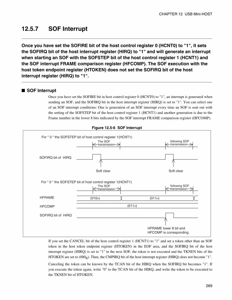
CHAPTER 12 USB Mini-HOST
12.5.7 SOF Interrupt
Once you have set the SOFIRE bit of the host control register 0 (HCNT0) to "1", it sets the SOFIRQ bit of the host interrupt register (HIRQ) to "1" and will generate an interrupt when starting an SOF with the SOFSTEP bit of the host control register 1 (HCNT1) and the SOF interrupt FRAME comparison register (HFCOMP). The SOF execution with the host token endpoint register (HTOKEN) does not set the SOFIRQ bit of the host interrupt register (HIRQ) to "1".
SOF InterruptOnce you have set the SOFIRE bit in host control register 0 (HCNT0) to "1", an interrupt is generated when
sending an SOF, and the SOFIRQ bit in the host interrupt register (HIRQ) is set to "1". You can select one
of an SOF interrupt conditions: One is generation of an SOF interrupt every time an SOF is sent out with
the setting of the SOFSTEP bit of the host control register 1 (HCNT1) and another generation is due to the
Frame number in the lower 8 bits indicated by the SOF interrupt FRAME comparison register (HFCOMP).
Figure 12.5-6 SOF Interrupt
If you set the CANCEL bit of the host control register 1 (HCNT1) to "1" and set a token other than an SOF
token in the host token endpoint register (HTOKEN) in the EOF area, and the SOFIRQ bit of the host
interrupt register (HIRQ) is set to "1" in the next SOF, the token is not executed and the TKNEN bits of the
HTOKEN are set to (000B). Then, the CMPIRQ bit of the host interrupt register (HIRQ) does not become "1".
Canceling the token can be known by the TCAN bit of the HIRQ when the SOFIRQ bit becomes "1". If
you execute the token again, write "0" to the TCAN bit of the HIRQ, and write the token to be executed to
the TKNEN bit of HTOKEN.
SOFIRQ bit of HIRQ
Soft clear Soft clear
HFRAME
HFCOMP
SOFIRQ bit of HIRQ
For " 0 " the SOFSTEP bit of host control register 1(HCNT1)
For " 0 " the SOFSTEP bit of host control register 1(HCNT1)
The SOF transmission
following SOF transmission
The SOF transmission
following SOF transmission
(010H) (011H)
(011H)
HFRAME lower 8 bit andHFCOMP is corresponding.
269

CHAPTER 12 USB Mini-HOST
If you set the CANCEL bit of host control register 1 (HCNT1) to "0", the token set in the host token
endpoint register (HTOKEN) is executed after the SOF is sent.
Figure 12.5-7 Example of Token Cancel Operation when CANCEL Bit of HCNT1 is "1".
Figure 12.5-8 Example of Token Cancel Operation when CANCEL Bit of HCNT1 is "0".
EOF areaSOFexecution
SOFIRQ bit of HIRQ
TKNEN bit of HTOKEN (000B) (010B) (000B)
CMPIRQ bit of HIRQ "0"
IN TOKEN write
EOF areaSOFexecution
IN TOKENexecution
SOFIRQ bit of HIRQ
TKNEN bit of HTOKEN (000B) (010B) (000B)
CMPIRQ bit of HIRQ
IN TOKEN write
270

CHAPTER 12 USB Mini-HOST
12.5.8 Error Status
USB Mini-HOST supports various error information.
Error Status
Stuffing error
If continuous 6 bits happen to be "1", one bit of "0" should be inserted in somewhere in the sequence, but
the STUFF bit of the host error status register (HERR) is set to "1" as a stuffing error if continuous 7 bits of
"1" are detected. Please do "0" to the STUFF bit in the writing to clear this. If the next token is executed
without clearing the STUFF bit, it is updated at the termination of the next token.
Toggle error
When receiving an IN token, the TGERR bit in the host error register (HERR) is set to "1" if the toggle data
for the data packet and the TGGL bit of the host token endpoint register (HTOKEN) are compared and a
match is not detected. To clear the TGERR bit, write "0" to it of the host error register (HERR). If the next
token is executed without clearing the TGERR bit, it is updated at the termination of the next token.
CRC error
When receiving an IN token, data in the received data packet and CRC are calculated with the CRC
polynomial G(X)=X16+X15+X2+1, and if the remainder is not (800DH), then a CRC error is assumed to
happen and the CRC bit of the host error register (HERR) is set to "1". To clear the CRC bit, write "0" to it
of the host error register (HERR). If the next token is executed without clearing the CRC bit, it is updated
at the termination of the next token.
Time-out error
The TOUT bit of the host error status register (HERR) is set to "1" if a data packet or handshake is not
received in a given time, SE0 is detected in received data, or a stuffing error is detected. To clear the TOUT
bit, write "0" to it of the host error register (HERR). If the next token is executed without clearing the
TOUT bit, it is updated at the termination of the next token.
Receive error
If EP1 or EP2 is used as the reception buffer, the PKS bit of the EP1 control register (EP1C) or EP2 control
register (EP2C), respectively. If the received data is greater than that of the received packet size, the RERR
bit of the host error status register (HERR) is set to "1". To clear the RERR bit, write "0" to it of the host
error register (HERR). If the next token is executed without clearing the RERR bit, it is updated at the
termination of the next token.
271

CHAPTER 12 USB Mini-HOST
12.5.9 Packet End
When one packet terminates in USB Mini-HOST, if the CMPIRE bit of the host control register 0 (HCNT0) is "1", an interrupt is generated to set the CMPIRQ bit of the host interrupt register (HIRQ) to "1".
Packet End TimingWhen one packet terminates, an interrupt is generated in the following timing:
When the TKKEN bits of the host token end point register (HTOKEN) are (001B), (010B) or (011B)
(SETUP token, IN token, and OUT token)
Figure 12.5-9 CMPIRQ Bit Set Timing Example 1 of HOST Interrupt Register (HIRQ)
When the TKKEN bit of the host token end point register (HTOKEN) is (100B) (SOF token)
Figure 12.5-10 CMPIRQ Bit Set Timing Example 2 of HOST Interrupt Register (HIRQ) (SOF TOKEN)
To the TKNEN bit of HTOKENWrite
Token packet data packet handshake packet
J-ST TKN ADR ENDPT TGGL
: J State : Token : Address : Endpoint : Toggle
CMPIRQ bit(HIRQ)
J-ST Sync TKN ADR ENDPT CRC5 EOP J-ST Sync TGGL DATA CRC16 EOP J-ST Sync ACK EOP J-ST
Write
CMPIRQ bit(HIRQ)
J-ST TKN FRAME
:J State :Token :Frame Number
To the TKNEN bit of HTOKEN
J-ST Sync TKN FRAME CRC5 EOP J-ST
272

CHAPTER 12 USB Mini-HOST
12.5.10 Suspend Resume
USB Mini-HOST supports suspend and resume operations.
Suspend OperationWhen writing "1" to the SUSP bit of the host state status register (HSTATE),
• USB bus high impedance state
• Stop of circuit block where clock is not necessary
USB Mini-HOST follows the steps above, and puts the USB circuit in suspend status. When the USB
circuit is put in suspend status, it sets the SUSP bit of the host state status register (HSTATE) to "1".
It is inhibited for USB Mini-HOST to set the USB circuit to suspend status or stop clock supplied to the
circuit when the USB bus is being reset or the SOFBUSY of HSTATE is "1" or data is being sent or
received.
Resume OperationBefore it can start resume operation in suspend status, one of the following conditions must be true:
(1) Write "0" to the SUSP bit of the host state status register (HSTATE).
(2) The pins D+ and D- for Mini-Host are detected to be k-state.
(3) The device is detected being cut.
(4) The device is detected being connected.
After the RWKIRQ bit of the host interrupt register (HIRQ) is set to "1", an issuance of the token is
allowed. The following show the operation timing for each condition.
273
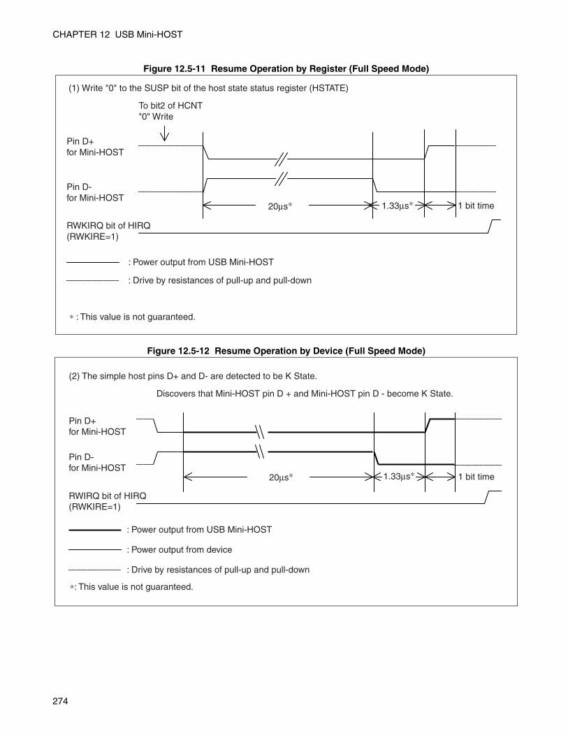
CHAPTER 12 USB Mini-HOST
Figure 12.5-11 Resume Operation by Register (Full Speed Mode)
Figure 12.5-12 Resume Operation by Device (Full Speed Mode)
To bit2 of HCNT"0" Write
RWKIRQ bit of HIRQ(RWKIRE=1)
Pin D+ for Mini-HOST
Pin D- for Mini-HOST
: Power output from USB Mini-HOST
: Drive by resistances of pull-up and pull-down
∗ : This value is not guaranteed.
1.33µs∗20µs∗ 1 bit time
(1) Write "0" to the SUSP bit of the host state status register (HSTATE)
Discovers that Mini-HOST pin D + and Mini-HOST pin D - become K State.
Pin D+ for Mini-HOST
Pin D- for Mini-HOST
RWIRQ bit of HIRQ(RWKIRE=1)
: Power output from USB Mini-HOST
: Power output from device
: Drive by resistances of pull-up and pull-down
∗: This value is not guaranteed.
1.33µs∗20µs∗ 1 bit time
(2) The simple host pins D+ and D- are detected to be K State.
274

CHAPTER 12 USB Mini-HOST
Figure 12.5-13 Resume Operation by Device Cutoff
Figure 12.5-14 Resume Operation by Device Connection
The device is detected being cut.
Cutting
Pin D+ for Mini-HOST
Pin D- for Mini-HOST
RWKIRQ bit of HIRQ(RWKIRE=1)
HIRQ bit0(DIRE=1)
CSTAT bit of HSTATE
Interruptoccurs
2.5µs or more
: Drive by resistances of pull-up and pull-down
(3) The device is detected being cut.
Pin D+ for Mini-HOST
Pin D- for Mini-HOST
RWKIRQ bit of HIRQ(RWKIRE=1)
HIRQ bit2(DIRE=1)
CSTAT bit of HSTATE
Interrupt occurs
2.5µs or more
: Drive by resistances of pull-up and pull-down
Connect
(4) The device is detected being connected.
275

CHAPTER 12 USB Mini-HOST
12.5.11 Cutting of Device
Once both Mini-HOST pins D + and D- become "L", the disconnection timer starts, and sets the CSTAT bit of the host state status register (HSTATE) to "0" when both pins detect "L" for 2.5µs or longer.
Cutting of DeviceRegardless of Mini-Host mode and function mode, when both Mini-Host pins D+ and D- detect "L" for
2.5µs or longer, it determines that the device is cut. Therefore, the CSTAT bit of the host state status
register (HSTATE) becomes "0", and the DIRQ bit of the host interrupt register (HIRQ) is set to "1". If the
DIRE bit of the host control register 0(HCNT0) is "1", an interrupt generates. To clear the interrupt, write
"0" to the DIRQ bit of the HIRQ.
When a reset is performed on the USB bus, it determines that the device is disconnected and sets the
CSTAT bit of the host state status register 0 (HSTATE) to "0", but the DIRQ bit of the host interrupt
register (HIRQ) does not become "1".
276

CHAPTER 12 USB Mini-HOST
12.6 Each Token Flow Chart of USB Mini-HOST
The flow chart of each token of USB Mini-HOST is as follows.
IN, OUT, SETUP Token
Figure 12.6-1 Flow Chart at IN, OUT, SETUP Token
IN TOKEN
END
NO
NO
NO
NO
YES
YES
YES
YES
YES
YES
NO
NO
YESYES
NO
NO
YES
NO
IN,OUT,SETUP TOKEN
HADR change?
HADR change
EP1 PKSchange?
EP2C PKS change?
PKS change
Buffer direction change
Buffer directionOK?
Set toggle and Endpoint,Execute TOKEN
Set Buffer usable
Buffer usable?
CMPIRQ of HIRQ=1?
EP1 DIR=1? EP1 DIR=1?
277

CHAPTER 12 USB Mini-HOST
SOF Token
Figure 12.6-2 Flow Chart at SOF Token
TOKEN execution
END
YES
YES
YES
NO
NO
NO
SOF TOKEN
HFRAMEchange?
HFRAME change
HEOF change
HEOF change?
CMPIRQ of HIRQ=1?
(Setting TGGL and ENDPT is disregarded.)
278

CHAPTER 13PWC TIMER
This chapter describes an overview of PWC timer, the configuration and function of register, and the PWC timer operation and precaution.
13.1 Overview of PWC Timer
13.2 Register of PWC Timer
13.3 Movement of PWC Timer
13.4 Precautions when Using PWC Timer
279

CHAPTER 13 PWC TIMER
13.1 Overview of PWC Timer
The PWC timer is the multi-functional 16-bit up count timer that has the function to measure the pulse width of input signal.PWC: Pulse Width Count (pulse width measurement)
Function of PWC TimerFollowing functions are implemented by hardware of a single channel including a 16-bit up count timer, a
register to control input pulse divider and division ratio, a measurement input terminal, and a 16-bit control
register:
Timer Functions
• The set interval interrupt request can be generated.
• Standard internal clock can be selected from three types.
Pulse width measurement function
• The time interval between arbiter events of external pulse input is measured.
• Standard internal clock can be selected from three types.
• Each kind of measurement mode
- "H" pulse width(↑ - ↓)/"L" pulse width(↑ - ↓)
- Rising cycle(↑ - ↑)/falling cycle(↓ - ↓)
- Measurement between edges(↑ or ↓ to ↓ or ↑)
• The 8-bit input divider enables the division measurement by dividing the input pulses with a
denominator of 22n (n = 1, 2, 3, or 4).
• You can make an interrupt occur at the end of measurement.
• You can select either a single measurement or continuous measurements.
280

CHAPTER 13 PWC TIMER
Block Diagram of PWC TimerFigure 13.1-1 shows the PWC timer block diagram.
Figure 13.1-1 Block Diagram of PWC Timer
Errordetection
Internal clock (Machine clock/4)
Reload
Data transmit
Overflow Clock16-bit Up count timer
Clock divider
8-bitdivider
Timer clear
Count enabled Divider clear
Inputwaveformcomparator
Ratio selection
Division ON/OFF
Control circuit
Edgedetection
Fla
g se
t etc
.
Con
trol
bit
outp
ut
Measurement end interrupt request
Measurement end edge
Start edge selection
End edge selection
Overflow interrupt request
Measurement start edge
PWCR readERR
PWCR
15PWCSR
PIS0/PIS1
ERR CKS0/CKS1
DIVR2
F2M
C-16 B
us
16
16
CKS1/CKS0
22
23
PWC
281

CHAPTER 13 PWC TIMER
13.2 Register of PWC Timer
Configuration and function of the register used for PWC timer are described.
Register List of PWC TimerFigure 13.2-1 shows the PWC timer register list.
Figure 13.2-1 Register List of PWC Timer
15 8 7 0
PWCSR
PWCR
DIVR
(R/W)
(R/W)
(R/W)
15 14 13 12 11 10 9 8
7 6 5 4 3 2 1 0
STRT STOP EDIR EDIE OVIR OVIE ERR Reserved
(R/W) (R/W) (R) (R/W) (R/W) (R/W) (R) (R/W)
(R/W) (R/W) (R/W) (R/W) (R/W) (R/W) (R/W) (R/W)CKS1 CKS0 PIS1 PIS0 S/C MOD2 MOD1 MOD0
15 14 13 12 11 10 9 8
7 6 5 4 3 2 1 0
(R/W) (R/W) (R/W) (R/W) (R/W) (R/W) (R/W) (R/W)
(R/W) (R/W) (R/W) (R/W) (R/W) (R/W) (R/W) (R/W)
D15 D14 D13 D12 D11 D10 D9 D8
D7 D6 D5 D2D3D4 D0D1
7 6 5 4 3 2 1 0
( − ) ( − ) ( − ) ( − ) ( − ) ( − ) (R/W) (R/W)
− − − − − − DIV0DIV1
00005DH
00005CH
00005FH
00005EH
000060H
R/WR
−
: Readable/Writable: Read only
: Undefined
PWCSRPWC control status registerInitial value 0000000XB
PWCSRPWC control status registerInitial value 00000000B
PWCRPWC data buffer registerInitial value 00000000B
PWCRPWC data buffer registerInitial value 00000000B
DIVRPWC ratio of dividing frequency control registerInitial value ------00B
282

CHAPTER 13 PWC TIMER
13.2.1 PWC Control Status Register (PWCSR)
Configuration and function of PWC control status register (PWCSR) are described.
PWC Control Status Register (PWCSR)Figure 13.2-2 shows the bit configuration of PWC control status register (PWCSR).
Figure 13.2-2 Bit Configuration of PWC Control Status Register (PWCSR)
The function of each bit in the PWC control status register (PWCSR) is described in the following.
[bit15, bit14] STRT, STOP (Timer Start Bit, Timer Stop Bit)
This bit controls to start, restart, and stop the 16-bit up count timer. Timer operation status is displayed
when reading.
The table below shows the function of STRT and STOP bit.
15 14 13 12 11 10 9 8
7 6 5 4 3 2 1 0
STRT STOP EDIR EDIE OVIR OVIE ERR Reserved
(R/W) (R/W) (R) (R/W) (R/W) (R/W) (R) (R/W)
(R/W) (R/W) (R/W) (R/W) (R/W) (R/W) (R/W) (R/W)CKS1 CKS0 PIS1 PIS0 S/C MOD2 MOD1 MOD0
00005DH
00005CH
PWCSRPWC control status registerInitial value 0000000XB
PWCSRPWC control status registerInitial value 00000000B
R/WR
−
: Readable/Writable: Read only
: Undefined
Table 13.2-1 Functions for Write Operation (Controlling the 16-bit Up Count Timer Operation)
STRT STOP Operation control functions
0 0 The influence is not in the function none/the operation.
0 1 Timer start/restart (count enabled).*
1 0 Timer operation forced stop (count disabled). *
1 1 The influence is not in the function none/the operation.
*: Enable use for clear bit instruction.
283

CHAPTER 13 PWC TIMER
• Initialized to "0" at reset.
• Read and write are enabled. However, meanings are different between when writing and reading as
shown in Table 13.2-1 and Table 13.2-2.
• The value read by read-modify-write instructions is always "11B" regardless of the bit value.
• Note that no bit instruction can be used for reading in the operating status (reading always produces the
operating status) although the bit instruction (bit clear) can be used for either STRT or STOP bit to start
or stop the timer.
[bit13] EDIR (measurement end interrupt request flag)
This flag indicates the measurement termination in the pulse width measurement. When the
measurement termination interrupt factor is permitted (bit12: EDIE = 1) and this bit is set, the
measurement termination interrupt request occurs.
• Initialized to "0" at reset.
• Only reading is allowed.
• Bit values cannot be changed by writing.
[bit12] EDIE (measurement end interruption permission)
Measurement termination interrupt request during the pulse width measurement is controlled as shown
in the table below:
• Initialized to "0" at reset.
• Reading or writing is allowed.
Table 13.2-2 Functions for Read Operation (Displaying the 16-bit Up-count Timer Operation Status)
STRT STOP Operation control functions
0 0 Timer under suspension (unstarted or measurement completed). [initial value]
1 1 During timer count operating (during measurement).
EDIR Operation mode
Set factor Set when the pulse width measurement terminates (measured results are stored in PWCR).
Clear factor Because PWCR (measurement result) is read, it is clear.
EDIE Operation mode
0 Measurement end interrupt request output disabled (interrupt is not generated even if EDIR is set).[Initial value]
1 Measurement end interrupt request output enabled (interrupt is generated if EDIR is set).
284

CHAPTER 13 PWC TIMER
[bit11] OVIR (timer overflow interrupt request flag)
This flag indicates the 16-bit up count timer overflowed from FFFFH to 0000H. When the timer
overflow interrupt factor is permitted (bit10: OVIE = 1) and this bit is set, the timer overflow interrupt
request occurs.
• Initialized to "0" at reset.
• Reading and writing are allowed; however, only writing "0" is effective, while writing "1" causes no
changes in the bit value.
• The read value is "1" in the read-modify write instructions regardless of the bit value.
[bit10] OVIE (timer overflow interrupt request permission)
Measurement termination interrupt request during the pulse width measurement is controlled as shown
in the table below:
• Initialized to "0" at reset.
• Reading and writing are allowed.
[bit9] ERR (error flag)
This flag indicates the next measurement termination before reading the measured result in the PWCR
in the pulse width measurement in the continuous measurement mode. In this case, the PWCR value is
updated with the new measurement result and the previous measurement result is lost. The
measurement is continued regardless of the bit value.
• Initialized to "0" at reset.
• Only reading is allowed. Write operations have no effect.
[bit8] Reserved bit
It is Reserved bit. Be sure to write "0".
OVIR Operation mode
Set factor Set when the overflow generates (FFFFH to 0000H).
Clear factor It is clear because of "0" writing or µDMAC.
OVIE Operation mode
0 Overflow interrupt request output disabled (interrupt is not generated even if OVIR is set). [Initial value]
1 Overflow interrupt request output enabled (interrupt is generated when OVIR is set).
ERR Operation mode
Set factor Set when measurement results that are not read yet are erased due to the next result.
Clear factor Because PWCR (measurement result) is read, it is clear.
285

CHAPTER 13 PWC TIMER
[bit7, bit6] CKS1 and CKS0 (clock selection)
Internal count clock can be selected from three types shown in Table 13.2-3.
• Initialized to 00B at reset.
• Read and write are enabled. However, setting "11B" is a interdiction.
Note:
Rewriting after the startup is an interdiction. Always perform the write operation before start or afterstop.
[bit5, bit4] PIS1, PIS0 (pulse width measurement input terminal selection)
The pulse width measurement input terminal is selected.
• Initialized to 00B at reset.
• Read and write are enabled. However, do not set "01B", "10B", and "11B".
Note:
Rewriting after the startup is an interdiction. Always perform the write operation before start or afterstop.
Table 13.2-3 Count Clock of 16 Bit Up Count Timer
CKS1 CKS0 Operation mode
0 0 Clock of machine clock divided by 4 (0.17µs for 24 MHz machine clock) [Initial value]
0 1 Clock of machine clock divided by 16 (0.67µs for 24 MHz machine clock)
1 0 Clock of machine clock divided by 32 (1.337µs for 24 MHz machine clock)
1 1 Setting disabled (Undefined)
Table 13.2-4 Selection of Pulse Width Measurement Input Terminal
PIS1 PIS0 Operation mode
0 0 (The terminal PWC is selected.) [Initial value]
0 1 Setting disabled
1 0 Setting disabled
1 1 Setting disabled (Undefined)
286

CHAPTER 13 PWC TIMER
[bit3] S/C (Measurement mode (single/continuous) selection)
The measurement mode is selected.
• Initialized to "0" at reset.
• Reading and writing are allowed.
Note:
Rewriting after the startup is an interdiction. Always perform the write operation before start or afterstop.
[bit2 to bit0] MOD2, MOD1, MOD0 (operation mode/measurement edge selection)
Operation mode and width measurement edge are selected.
• Initialized to "00B" at reset.
• Reading and writing are allowed.
Note:
Rewriting after the startup is an interdiction. Always perform the write operation before start or afterstop.
Table 13.2-5 Selection of Measurement Mode of 16-bit Up-count Timer
S/C Measurement mode selection At timer mode Pulse width
0 Single measurement mode [Initial value]
Reload none (single shot) Stop after one measurement
1 Continuous measurement mode There is reload (reload timer).Continuous measurement: buffer register enabled
Table 13.2-6 Selection of Operating Mode/measurement Edge of 16-bit Up-count Timer
MOD2 MOD1 MOD0 Operation mode/measurement edge selection
0 0 0 Timer mode [Initial value]
0 0 1 Timer mode (only Reload mode)
0 1 0 Pulse width measurement mode between all edges (↑ or ↓ - ↓ or ↑)
0 1 1 Divided cycle measurement mode (input divisor enabled)
1 0 0 Cycle between rising edges measurement mode (↑ - ↑)
1 0 1 "H" pulse width measurement mode (↑ - ↓)
1 1 0 "L" pulse width measurement mode (↓ - ↑)
1 1 1 Cycle between falling edges measurement mode (↓ - ↓)
287

CHAPTER 13 PWC TIMER
13.2.2 PWC Data Buffer Register (PWCR)
Configuration and function of PWC data buffer register (PWCR) are described.
PWC Data Buffer Register (PWCR)Figure 13.2-3 shows the bit configuration of PWC data buffer register (PWCR).
Figure 13.2-3 Bit Configuration of PWC Data Buffer Register (PWCR)
The function of PWC data buffer register (PWCR) varies in between the timer mode and the pulse width
setting mode that are set by the PWCSR register bit2 to "0" (MOD2 to MOD0).
In the timer mode (read/write enabled)
Becomes the reload register that holds the reload data when the reload timer operates (PWCSR bit3: S/C =
1). It is reading/writing in this case, it is possible in both writing.
Becomes a direct access to the up count timer in the one-shot timer operation mode (PWCSR bit3: S/C =
0). Perform the write operation when the timer stops although either read or write is possible also in this
case. Reading is always enabled to read the timer value in the count operation.
In the pulse width measurement mode (read only enabled)
Becomes the buffer register that holds the previous measurement result in the continuous measurement
mode (PWCSR bit3: S/C = 1).
In this case, the read only is enabled and no register value will be changed even when writing.
Becomes a direct access to the up count timer in the single mode (PWCSR bit3: S/C = 0).
Also in this case, the read only is enabled and no register value will be changed even when writing.
Reading is anytime enabled to obtain the timer value during the count operation. When the measurement is
finished, the measured value is held.
Note:
Please access the PWCR register by word move operation. Be initialized to "00B" when resetting.
15 14 13 12 11 10 9 8
7 6 5 4 3 2 1 0
(R/W) (R/W) (R/W) (R/W) (R/W) (R/W) (R/W) (R/W)
(R/W) (R/W) (R/W) (R/W) (R/W) (R/W) (R/W) (R/W)
D15 D14 D13 D12 D11 D10 D9 D8
D7 D6 D5 D2D3D4 D0D1
00005FH
00005EH
PWCRPWC data buffer registerInitial value 00000000B
PWCRPWC data buffer registerInitial value 00000000B
R/W : Readable/Writable
288

CHAPTER 13 PWC TIMER
13.2.3 PWC Ratio of Dividing Frequency Control Register (DIVR)
Configuration and function of PWC Ratio of dividing frequency control register (DIVR) are described.
PWC Ratio of Dividing Frequency Control Register (DIVR)Figure 13.2-4 shows the bit configuration of a PWC ratio of dividing frequency control register (DIVR).
Figure 13.2-4 Bit Configuration of PWC Ratio of Dividing Frequency Control Register (DIVR)
[bit7 to bit2] Undefinition bit
The reading value is irregular. No effect on writing.
[bit1, bit0] DIV1, DIV0 (division ratio selection)
This register is used in the division cycle measurement mode (PWCSR bit2, bit1, bit0: MOD2, MOD1,
MOD0 = 001B) and has no meaning in the other mode else.
In the division cycle measurement mode, pulses input to the measurement terminal are divided by the
division ratio set in the DIVR register and a single cycle width is measured after dividing.
• Initialized to "00B" at reset.
• Reading and writing are allowed.
Note:
Rewriting after the startup is an interdiction. Always perform the write operation before start or afterstop.
R/W : Readable/Writable
− : Undefined
7 6 5 4 3 2 1 0
( − ) ( − ) ( − ) ( − ) ( − ) ( − ) (R/W) (R/W)
− − − − − − DIV0DIV1000060HDIVRPWC ratio of dividing frequency control registerInitial value ------00B
Table 13.2-7 Division Ratio Selection
DIV1 DIV0 Count clock selection
0 0 4-dividing frequency [Initial value]
0 1 16-frequency division
1 0 64-frequency division
1 1 256-frequency division
289

CHAPTER 13 PWC TIMER
13.3 Movement of PWC Timer
The movement of the PPG timer is explained.
Outline of PWC Timer OperationThe PWC timer, a multi-functional timer based on the 16-bit up count timer has built-in measurement input
terminal, 8-bit input division, etc. PWC timer has the following two main functions:
• Timer Functions
• Pulse width count function
Either function can select three kinds of count clocks. Basic performance and operation of each function are
described as follows:
290

CHAPTER 13 PWC TIMER
13.3.1 Operation of PWM Timer Functions
The up count timer enables the reload and one-shot operations.
Operation of PWM Timer FunctionsPerforms the count up at every count clock after starting the timer. An interrupt request may occur when an
overflow occurs in the range between 0000H and FFFFH.
The following operation is executed due to the mode when an overflow occurs:
• One-shot mode: Stops Counting
• Reload mode: The contents of reload register is reloaded to the timer and the counting restarts.
Figure 13.3-1 shows the timer function operation in the one-shot and reload modes.
Figure 13.3-1 Operation of Timer Functions
[One-shot mode]
[Reload mode]
Overflow
Overflow Overflow Overflow Overflow Overflow
Overflow
Time
Time
Timer count value
Timer count value
ReloadReload Reload Reload
Reload
RestartPWCR write Timer start
Timer start Timer start
Timer stop
PWCR write value
OVIR flag set
OVIR flag set/Timer stop OVIR flag set/Timer stop
(Restart disabled)
Write to PWCR
(A solid line shows the timer count value.)
Reload
Reload
FFFFH
0000H
FFFFH
0000H
291

CHAPTER 13 PWC TIMER
13.3.2 Operation of Pulse Width Measurement Function
Time cycle between arbiter events of input pulse can be measured by the time.
Operation of Pulse Width Measurement FunctionThe pulse width measurement function does not start the count until the set measurement start edge is input
after it is started. Starts the count up after clearing the timer to be 0000H when detecting the start edge and
stops the count when detecting the stop edge. The value counted in this period is registered as the pulse
width. When the measurement ends, the interruption is detected.
Operates as follows depending on the measurement mode after the measurement.
• Single measurement mode: Suspends the operation.
• Continuous measurement mode:The timer value is transferred to the buffer register and the
measurement is suspended until the next start edge is input.
Figure 13.3-2 and Figure 13.3-3 show the single measurement mode operation and the continuous measurement
mode operation, respectively.
Figure 13.3-2 Pulse Width Measurement Operation (Single Measurement Mode/ "H" Width Measurement)
Figure 13.3-3 Pulse Width Measurement Operation (Continuous Measurement Mode/ "H" Width Measurement)
Timer count value
EDIR flag set (Measurement end)Time
Timer clear
Measurementstart
Timerstart
Timerstop
(A sold line shows the timer count value.)
PWC input measured pulse
FFFFH
0000H
Timer count value
Time
EDIR flag setEDIR flag set (Measurement end)
Timer clearTimer clear
Measurementstart
Timerstart
Timerstart
Timerstop
Overflow
(A solid line shows the timer count value.)
PWC input measured pulse
Transfer data to PWCRFFFFH
0000H
292

CHAPTER 13 PWC TIMER
13.3.3 Count Clock Selection and Operation Mode Selection
Count clock selection and operation mode selection are described.
Count Clock SelectionTimer count clock can be selected from three types of internal clock sources by setting the RWCSR bit7
(CKS1) and bit6 (CKS0).
Table 13.3-1 shows the count clock selection contents.
• 4-division clock of machine clock is selected for the initial value after the reset.
Note:
Select the count clock always before starting the timer.
Table 13.3-1 Count Clock Selection Contents
PWCSR/bit7,bit6:CKS1,CKS0
Selected internal count clock
00B4-division of Machine clock(0.17µs in case of machine clock of 24 MHz) [Initial value]
01B16-division of Machine clock(0.67µs in case of machine clock of 24 MHz)
10B32-division of Machine clock(1.33µs in case of machine clock of 24 MHz)
293
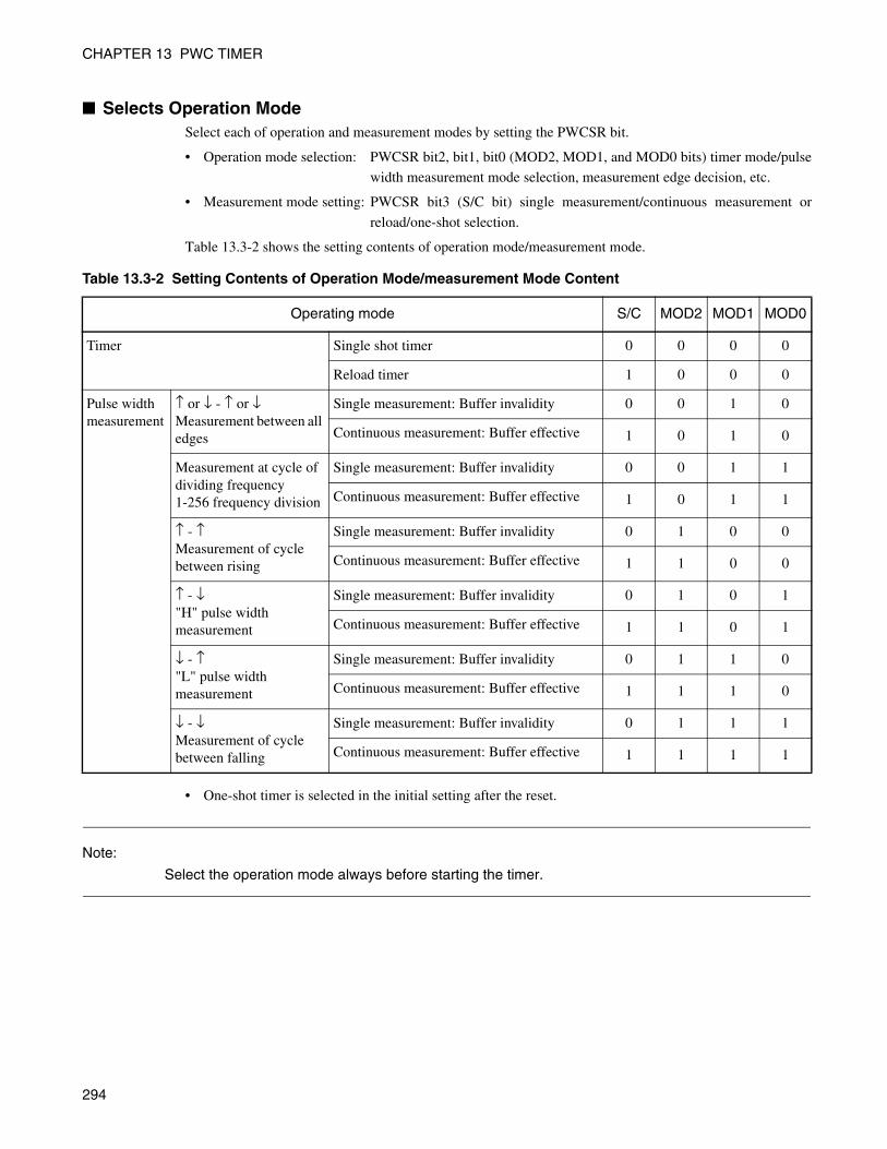
CHAPTER 13 PWC TIMER
Selects Operation ModeSelect each of operation and measurement modes by setting the PWCSR bit.
• Operation mode selection: PWCSR bit2, bit1, bit0 (MOD2, MOD1, and MOD0 bits) timer mode/pulse
width measurement mode selection, measurement edge decision, etc.
• Measurement mode setting: PWCSR bit3 (S/C bit) single measurement/continuous measurement or
reload/one-shot selection.
Table 13.3-2 shows the setting contents of operation mode/measurement mode.
• One-shot timer is selected in the initial setting after the reset.
Note:
Select the operation mode always before starting the timer.
Table 13.3-2 Setting Contents of Operation Mode/measurement Mode Content
Operating mode S/C MOD2 MOD1 MOD0
Timer Single shot timer 0 0 0 0
Reload timer 1 0 0 0
Pulse width measurement
↑ or ↓ - ↑ or ↓ Measurement between all edges
Single measurement: Buffer invalidity 0 0 1 0
Continuous measurement: Buffer effective 1 0 1 0
Measurement at cycle of dividing frequency1-256 frequency division
Single measurement: Buffer invalidity 0 0 1 1
Continuous measurement: Buffer effective 1 0 1 1
↑ - ↑ Measurement of cycle between rising
Single measurement: Buffer invalidity 0 1 0 0
Continuous measurement: Buffer effective 1 1 0 0
↑ - ↓ "H" pulse width measurement
Single measurement: Buffer invalidity 0 1 0 1
Continuous measurement: Buffer effective 1 1 0 1
↓ - ↑ "L" pulse width measurement
Single measurement: Buffer invalidity 0 1 1 0
Continuous measurement: Buffer effective 1 1 1 0
↓ - ↓ Measurement of cycle between falling
Single measurement: Buffer invalidity 0 1 1 1
Continuous measurement: Buffer effective 1 1 1 1
294
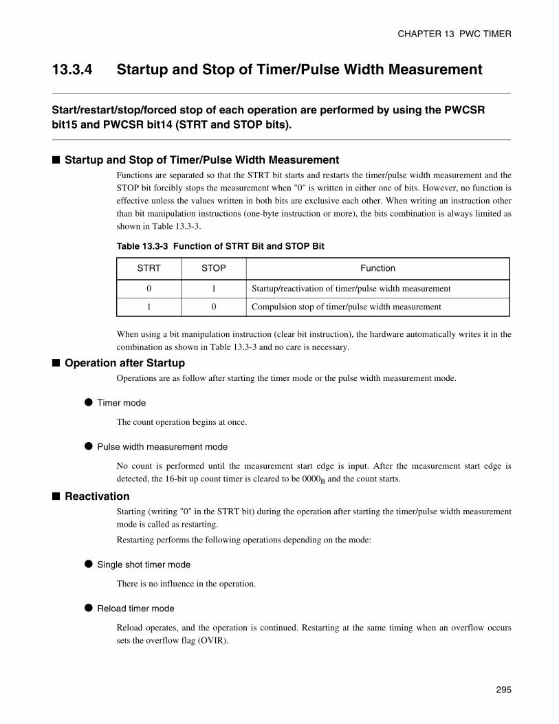
CHAPTER 13 PWC TIMER
13.3.4 Startup and Stop of Timer/Pulse Width Measurement
Start/restart/stop/forced stop of each operation are performed by using the PWCSR bit15 and PWCSR bit14 (STRT and STOP bits).
Startup and Stop of Timer/Pulse Width MeasurementFunctions are separated so that the STRT bit starts and restarts the timer/pulse width measurement and the
STOP bit forcibly stops the measurement when "0" is written in either one of bits. However, no function is
effective unless the values written in both bits are exclusive each other. When writing an instruction other
than bit manipulation instructions (one-byte instruction or more), the bits combination is always limited as
shown in Table 13.3-3.
When using a bit manipulation instruction (clear bit instruction), the hardware automatically writes it in the
combination as shown in Table 13.3-3 and no care is necessary.
Operation after StartupOperations are as follow after starting the timer mode or the pulse width measurement mode.
Timer mode
The count operation begins at once.
Pulse width measurement mode
No count is performed until the measurement start edge is input. After the measurement start edge is
detected, the 16-bit up count timer is cleared to be 0000B and the count starts.
ReactivationStarting (writing "0" in the STRT bit) during the operation after starting the timer/pulse width measurement
mode is called as restarting.
Restarting performs the following operations depending on the mode:
Single shot timer mode
There is no influence in the operation.
Reload timer mode
Reload operates, and the operation is continued. Restarting at the same timing when an overflow occurs
sets the overflow flag (OVIR).
Table 13.3-3 Function of STRT Bit and STOP Bit
STRT STOP Function
0 1 Startup/reactivation of timer/pulse width measurement
1 0 Compulsion stop of timer/pulse width measurement
295

CHAPTER 13 PWC TIMER
Pulse width measurement mode
In the state of measurement starting edge waiting there is no influence in the operation. During the
measurement, the count is stopped and the measurement start edge is again waited. In this case, if the
measurement termination edge detection and the restart occur at the same time, the measurement
termination flag (EDIR) is set and the result is transferred to PWCR in the continuous measurement mode.
StopsIn the one-shot timer mode and the single measurement mode, the timer overflow or the measurement
termination automatically stops the count and no intentional stop is necessary. In the other modes, however,
the timer must be forcibly stopped. Similarly, if you want to stop the timer before the automatic stop, you
must forcibly stop it.
Check Operating StateWhen the above-mentioned STRT and STOP bits are read, they are functional as the operating state
indication bits.
Table 13.3-4 shows the function of operating state indication bit.
Note:
Reading either the STRT or STOP bit provides a same value. Do not use, however, the read-modify-write instructions (bit process instructions, etc.) to read the STRT and STOP bits because "11B"always results.
Table 13.3-4 Function of Operating State Indication Bit
STRT STOP Operating State
0 0 Timer stop (excluding status of waiting for measurement start edge):It is not active or shows that the measurement ended.
1 1 During timer counting or waiting for measurement start edge
296

CHAPTER 13 PWC TIMER
13.3.5 Operation of Timer Mode
The operation of the timer mode is explained.
Clearing TimerThe 16-bit up count timer is cleared to be 0000H in the following case:
• At a reset
• In the pulse width measurement mode, when the measurement start edge is detected and the count is
started.
One-shot Operation ModesIn the one-shot operation mode, the count up is performed at every count clock after the timer started and
an overflow occurrence at counting from FFFFH to 0000H automatically stops the count. When a value is
set in the PWCR before starting the timer, the count is started from the value. In this case, the set value is
not held and the PWCR value indicates the current count value.
Reload Operation ModeIn the reload operation mode, the count up is performed at every count clock after the reload value in the
PWCR is set in the timer after starting the timer. Overflow occurrence at counting from FFFFH to 0000H
again sets the reload value in the PWCR in the timer (reload operation) to repeat the count operation. The
timer does not stop until it is forcibly stopped by writing into the PWCSR STOP bit or it is reset. The value
set in the PWCR before starting the timer is held as the reload value during the count operation and always
set in the timer at starting/restarting and an overflow occurrence. Use a newly changed reload value to
change the set value during the count operation at the next overflow occurrence or the timer restarting.
Timer Value and Reload ValueThe PWCR in the one-shot operation mode has a direct access to the up count timer. The value written in
the PWCR is written in the timer as it is so that you can acquire the timer value in the count operation by
reading the PWCR value during the timer operation. If you write an arbiter value in the PWCR before
starting the timer, the count operation is started from this specified value. In the reload operation mode,
accessing the up count timer is impossible. The PWCR functions as the reload register to hold the reload
value. When the timer start, restart, or overflow occurs, the value written in the PWCR always set to the
timer. When PWCR is read, the stored reload value is read.
The PWCR value and the timer value are undefined when the timer is set to the one-shot operation mode
after forcibly suspending the reload operation mode. Therefore, always write the value before using the
timer.
Interrupt Generation RequestIn timer mode operation, interrupt request by the timer overflow can be generated. An interrupt request is
generated when the overflow flag is set at an overflow occurrence caused by the count up and the overflow
interrupt request is permitted.
297

CHAPTER 13 PWC TIMER
Timer CycleIf 0000H is set to the PWCR in the one-shot operation mode and the timer is started, an overflow occurs
after 65536 times counted up to stop the count. The time period from the start to the stop is calculated by
the following expression:
T1=(65536-n1) • t
T1: Time from startup to stop (µs)
n1: Timer value written in the PWCR at the start
t: Count Clock cycle (µs)
If 0000H is set to the PWCR in the reload operation mode and the timer is started, an overflow occurs at
every 65536-time counted up. Reload cycle time is calculated by the following expression:
TR=(65536-nR) • t
TR: Reload cycle (overflow cycle) (µs)
nR: Reload value held in the PWCR
t: Count Clock cycle (µs)
Count Clock and Maximum CycleMaximum cycle is provided when 0000H is set for the PWCR value in the timer mode.
The count clock cycle and the maximum cycle of the timer are shown in Table 13.3-5 when the machine
clock frequency (called F hereafter) is 24 MHz.
Table 13.3-5 Count Clock and Cycle
Count clock selection in CSK1,CSK0=00:(φ/4) in CSK1,CSK0=00:(φ/16) in CSK1,CSK0=00:(φ/32)
Count Clock Cycle 0.17 µs 0.67 µs 1.33 µs
Timer maximum cycle 10.92 ms 43.7 ms 87.4 ms
298

CHAPTER 13 PWC TIMER
Operation Flow of TimerFigure 13.3-4 shows the timer operation flow.
Figure 13.3-4 Operation Flow of Timer
Count stopOperation stop
Count up
Count start
Count up
Count start
Overflow generationOVIR flag set
Overflow generationOVIR flag set
Read PWCR value to Timer
Restart
One-shot operation modeReload operation mode
Set value to PWCR
Start by STRT bit
Each settings
Count clock selectionOperation/Measurement mode selectionInterrupt flag clearInterrupt enabled
299

CHAPTER 13 PWC TIMER
13.3.6 Operation of Pulse Width Measurement Mode
Operation of pulse width measurement mode is described.
Single Measurement and Continuous MeasurementPulse width measurement modes include a mode to perform only one-time measurement and a mode to
perform continuous measurements. Each mode is selected by the PWCSR S/C bits (see "13.3.3 Count
Clock Selection and Operation Mode Selection").
One-time measurement mode
When the first measurement termination edge is input, the timer counter stops and the measurement
termination flag (EDIR) in the PWCSR is set not to perform measurement anymore (however, when the
restart occurs at the same time, the measurement start is waited).
Continuous measurement mode
When the measurement termination edge is input, the timer counter stops and the measurement termination
flag (EDIR) in the PWCSR is set to stop the count until the measurement start edge is again input. When
the measurement start edge is again input, the measurement is started after the timer is cleared to 0000H. At
the measurement termination, the measured result in the timer is transferred to the PWCR.
Note:
Always change the measurement mode selection when the timer stops.
Data of Measurement ResultMeasured results, the timer value handling, and the PWCR function are different between the single
measurement mode and the continuous measurement mode. The measurement result in both modes is as
follows:
One-time measurement mode
• When the PWCR is read during the operation, the timer value in the measurement is acquired.
• When the PWCR is read after the measurement termination, the measured result data is acquired.
Continuous measurement mode
• At the measurement termination, the measured result in the timer is transferred to the PWCR.
• When the PWCR is read, the last measurement result is acquired and the previous measurement result is
held even in the measurement operation. The timer value under the measurement cannot be read.
When the next measurement is terminated before reading the measured result in the continuous
measurement mode, the previous measurement result is erased by a new measurement result. In this case,
the gill in PWCSR-Flag (ERR) is set. Error flag (ERR) is automatically cleared when reading the PWCR.
300

CHAPTER 13 PWC TIMER
Measurement Mode and Counter OperationThe measurement mode can be selected from six types depending on the place where the input pulse is
measured. The cycle measurement mode is also prepared to arbitrarily divide the input pulse for high-
precision measurement of higher frequency pulse width. Table 13.3-6 shows the measurement mode list.
Table 13.3-6 The Measurement Mode List (1/2)
Measurement mode
MOD2 MOD1 MOD0Measurement mode measured target
(W: width of a measured pulse)
"H" pulse width measurement
1 0 1
The width at "H" period is measured.Count (measurement) start: when detecting a rising edgeCount (measurement) end: when detecting a falling edge
"L" pulse width measurement
1 1 0
The width at "L" period is measured.Count (measurement) start: when detecting a falling edgeCount (measurement) end: when detecting a rising edge
RisingBetween edgesMeasurement at cycle
1 0 0
A cycle between rising edges is measured.Count (measurement) start: when detecting a rising edgeCount (measurement) end: when detecting a rising edge
FallingBetween edgesMeasurement at cycle
1 1 1
A cycle between falling edges is measured.Count (measurement) start: when detecting a falling edgeCount (measurement) end: when detecting a falling edge
Between all edges pulse width measurement
0 1 0
The width between the edges continuously input is measured.Count (measurement) beginning: When edge is detectedCount (measurement) end: When edge is detected
Count start Count stop Start Stop
W W
Count start Count stop Start Stop
W W
Count startCount stop
StartStart
StopStop
W W W
Count startCount stop
StartStart
StopStop
WWW
Count startCount stop
StartStart
StopStop
W W W
301

CHAPTER 13 PWC TIMER
No timer count is performed from start of the count to input of the count start edge in any modes. The timer
is cleared to 0000H after inputting the count start edge and the timer count is performed at every count
clock until the count termination edge is input. When the count termination edge is input, the next operation
is executed.
1. Measurement ending flag (EDIR) in PWCSR is set.
2. The timer count operation stops (excluding when it is at the same time of restarting).
3. Continuous measurement mode:The timer value (measured result) is transferred to the PWCR and the
count is suspended until the next measurement start edge is input.
4. Single measurement mode: The measurement is terminated (excluding when it is at the same time of
restarting).
When the pulse width measurement between all edges or the division measurement is performed in the
continuous measurement mode, the termination edge is the next measurement edge.
Minimum Input Pulse WidthThere are following limitations for pulses that can be input to width measurement input terminals (PWC).
Pulse width must be 4-machine cycle (0.17µs for the 24-MHz machine clock) or more.
Calculation Method of Pulse Width/cyclePulse width/cycle to be measured can be calculated by the following expression:
TW=n • t/DIV (µs)
TW: pulse width to be measured/cycle (µs)
n: Measurement result data in PWCR
t: Count Clock cycle (µs)
DIV: Division ratio selected by the division ratio register DIVR
(Frequency of dividing frequency measurement mode)
Measurement at cycle of dividing frequency
0 1 1
For only dividing ratio selected by division setting register DIVRThe input pulse is divided and the cycle is measured.Count (measurement) start: when detecting a rising edge immediately after
counting startsCount (measurement) end: when one cycle ends after it is divided
Table 13.3-6 The Measurement Mode List (2/2)
Measurement mode
MOD2 MOD1 MOD0Measurement mode measured target
(W: width of a measured pulse)
Count startCount stopStart Stop(Example of 4 division)
W W W
302

CHAPTER 13 PWC TIMER
Range of Count at Pulse Width/cycleMeasurable ranges of pulse width/cycle vary depending on the selected combination of division ratios of
count clock and input divider.
Table 13.3-7 shows the measurement range list of machine clock when the clock frequency (called Φhereafter) is 24 MHz.
Interrupt Request GenerationTwo following interrupt requests can be generated in the pulse width measurement mode:
Interrupt request by overflow of timer
When an overflow is generated by the count up during the measurement, the overflow flag is set. When the
overflow interrupt request is permitted, an interrupt request occurs.
Interrupt request by measurement termination
When the measurement termination edge is detected, the measurement termination flag (EDIR) in the
PWCSR is set. If the measurement termination interrupt request is permitted, the interrupt request occurs.
The measurement termination flag (EDIR) is automatically cleared as soon as the measured result PWCR is
read.
Table 13.3-7 Pulse Width Measurement Range List
Divide ratio DIV1 DIV0 in CKS1,CKS0=
00(φ/4)in CKS1,CKS0=
01(φ/16)in CKS1,CKS0=
10(φ/32)
None - -0.17 µs to 10.92 ms
(0.25 µs) 0.17 µs to 43.7 ms
(1.6 µs) 0.17 µs to 87.4 ms
(3.2 µs)
4-frequency division 0 0 0.17 µs to 2.73 ms
(6.25 µs)0.17 µs to 10.92 ms
(0.4 µs)0.17 µs to 21.85 ms
(0.8 µs)
16-frequency division 0 1 0.17 µs to 683 µs
(15.6 ns)0.17 µs to 2.73 ms
(1.6 µs) 0.17 µs to 5.46 ms
(0.2 µs)
64-frequency division 1 0 0.17 µs to 170 µs
(3.91 µs)0.17 µs to 683 µs
(25 µs)0.17 µs to 1.36 ms
(50 ns)
256-frequency division 1 1 0.17 µs to 43 µs
(0.98 µs) 0.17 µs to 171 µs
(6.25 µs) 0.17 µs to 341 µs
(12.5 ns)
Note: These values enclosed in brackets ( ) indicate the granularity per bit
303

CHAPTER 13 PWC TIMER
Operation Flow of Pulse Width MeasurementFigure 13.3-5 shows the pulse width measurement operation flow.
Figure 13.3-5 Operation Flow of Pulse Width Measurement
Count up
Count start
Clear timer
Count up
Count start
Clear timer
Measurement edge detection
EDIR flag set
Operation stop
Count stop
Measurement edge detection
EDIR flag set
Count stop
Overflow generationOVIR flag set
Overflow generationOVIR flag set
Read Timer value to PWCR
Restart Start by STRT bit
Each settings
Count clock selectionOperation/Measurement mode selectionInterrupt flag clearInterrupt enabled
Measurement start edge detection
Measurement start edge detection
Continuous measurement mode
Singlemeasurement mode
304

CHAPTER 13 PWC TIMER
13.4 Precautions when Using PWC Timer
Precautions when using the PWC timer are described.
Precautions when Using PWC Timer
Notes concerning rewriting register
Following bits among PWCSRs are inhibited to be updated during the operation. Always update the bits
before starting or after stopping the operation.
• (bit7, bit6) CKS1,CKS0 (clock selection)
• (bit5, bit4) PIS1, PIS0 (input signal selection)
• (bit3) S/C (Measurement mode (single/continuous) selection)
• (bit2, bit1, bit0) MOD2, MOD1, MOD0 (operation mode/measurement edge selection)
It is inhibited to update the DIVR during the operation. Always update the bits before starting or after
stopping the operation.
Handling of measurement ending flag of timer mode
Measurement termination interrupt request flag (EDIR) value in the PWCSR has no meaning in the timer
mode. Therefore, always set "0" to the measurement termination interrupt request bit (EDIE) in the
PWCSR, when using in the timer mode.
Treatment of STRT and STOP bit in PWCSR
Note that both bits have different meaning between when writing and reading (see "13.2.1 PWC Control
Status Register (PWCSR)"). In addition, the read value is "11B" when using a read-modify-write instruction
regardless of the bit value. Therefore, note that no bit process instruction can be used to read the operating
status (reading always produces the operating status). When writing to the STRT and STOP bits to start/
stop the timer, bit process instruction (bit clear instruction, etc.) can be used for the respective bits.
Clearing Timer
Since the timer is cleared by the measurement start edge in the pulse width measurement mode, the data
present in the timer before starting become invalid.
Value of PWCR and timer when mode is changed
• Always write the value before using the timer because the held value in the PWCR and the timer value
become undefined when they are used in the reload timer mode before forcibly stopping the timer to
switch to the one-shot timer mode.
• Always write the value before the use because the PWCR value becomes undefined if it is used in the
one-shot timer mode.
• Always reset the value to the PWCR before starting the operation when switching the pulse width
measurement mode to the timer mode.
305

CHAPTER 13 PWC TIMER
Minimum pulse width
There are following limitations for pulses that can be input to width measurement input terminals:
• Minimum pulse width: 2 divisions of machine clock (0.25µs or more for 16-MHz machine clock)
• Minimum input frequency: 4 divisions of machine clock (4 MHz or less for 16-MHz machine clock)
When the input pulse width is smaller or the input pulse frequency is higher than the above description, the
operation cannot be guaranteed. If there is a possibility of such noise in the input signal, use, for example, a
filter outside of the chip to eliminate the noise before the signal is input.
Frequency of dividing frequency measurement mode
Note that the pulse width obtained from the measured result calculation is the average value because the
input pulses are divided in the division cycle measurement mode among the pulse width measurement
modes.
Handling of clock select bit
Do not set "11B" to (bit7, bit6) CKS1, CKS0 (clock selection) in the PWCSR.
Reactivation under operation
When restarting after starting the count operation, following cases may occur depending on the timing:
• When restarting at the same time of an overflow occurrence in the reload timer mode, the overflow flag
(OVIR) is set.
• When restarting at the same time of measurement termination edge input in the pulse width single
measurement mode, the measurement start edge is waited and the measurement termination edge
(EDIR) is set.
• When restarting at the same time of measurement termination edge input in the pulse width single
measurement mode, the measurement start edge is waited and the measurement termination edge
(EDIR) is set and the current measured result is transferred to the PWCR.
When the PWC timer is used in "the "H" pulse-width or "L" pulse-width measurement mode in the
continuous measurement mode":
The pulse width measurement is completed, the next pulse width measurement start is waited, the timer
operation is unexpectedly continued, and the overflow flag (OVIR) of timer may be sometime set before
starting the next pulse width measurement. In this case, even when no overflow occurs at the next pulse
width measurement termination, the overflow flag has been set. Therefore, do not use the overflow flag
when using the PWC timer in the "H" pulse width or "L" pulse width measurement mode in the continuous
measurement mode.
306

CHAPTER 1416-BIT RELOAD TIMER
This chapter describes an overview of 16-bit reload timer, the configuration and functions of register and the 16-bit reload timer operation.
14.1 Overview of 16-bit Reload Timer
14.2 Registers of 16-bit Reload Timer
14.3 Movement of 16-bit Reload Timer
307

CHAPTER 14 16-BIT RELOAD TIMER
14.1 Overview of 16-bit Reload Timer
The 16-bit reload timer provides two functions either one of which can be selected, the internal clock that performs the count down by synchronizing with 3-type internal clocks and the event count mode that performs the count down by detecting the arbiter edge of pulses input to the external terminal.
Overview of 16-bit Reload TimerUnderflow of the 16-bit reload timer is defined as a case when the count value becomes from 0000H to
FFFFH. Therefore, when the equation (reload register setting value + 1) holds, an underflow occurs. Either
mode can be selected for the count operation from the reload mode which repeats the count by reloading
the count setting value at the underflow occurrence or the one-shot mode which stops the count at the
underflow occurrence. The interrupt can be generated at the counter underflow occurrence so as to
correspond to the DTC.
308

CHAPTER 14 16-BIT RELOAD TIMER
14.1.1 Function of 16-bit Reload Timer
This section describes overview and Function of 16-bit reload timer.
Operation Modes of 16-bit Reload Timer
Internal Clock ModeOne type can be selected for the count clock from 3 types of internal clocks.
Software trigger operation
When 1 is written to TGR bit of timer control status register (TMCSR0), counter operation is started.
Trigger input using the TRG bit is valid for the external trigger input and the external gate input.
External trigger operation
When the selected edges (rising edge, falling edge, or both edges) are input to the TIN0 terminal, the count
operation is started.
External gate input operation
While the selected signal ("L" or "H") is being input to TIN0, the count operation is continued.
Event Count Mode (External Clock Mode) This function count downs at the edge when the selected edges (rising edge, falling edge, or both edges) are
input to the TIN0 terminal.
External clock of a constant cycle can be also used for the interval timer.
Clock Mode Counter operation 16-bit reload timer operation
Internal clockReload mode Software trigger operation
External trigger operationExternal gate input operationOne-shot mode
Event count mode(External clock Mode)
Reload modeSoftware trigger operation
One-shot mode
309

CHAPTER 14 16-BIT RELOAD TIMER
Counter Operation Mode
Reload mode
When an underflow (0000H → FFFFH) occurs during the count down, the count setting value is reloaded to
continue the count operation. Interrupt request that can be generated at the underflow occurrence can be
also used as an interval timer. The toggle waveform which reverses at every underflow occurrence can be
also output from the TOT0 terminal.
One-shot mode
When an underflow (0000H → FFFFH) occurs during the count down, the count operation is stopped.
The interruption can be generated by the underflow. Short waveform which indicates the count operation
can be also output from the TOT0 pin during the count operation.
Count Clock Count Clock Cycle Time of interval
Internal clock
21/ φ (0.083 µs) 0.083 µs to 5.461 ms
23/ φ (0.33 µs) 0.33 µs to 21.845 ms
25/ φ (1.33 µs) 1.33 µs to 87.38 ms
External clock 23/ φ (0.5 µs) 0.5 µs or more
φ: Machine clock values in parentheses ( ) are when machine clock is in 24 MHz operating.
310

CHAPTER 14 16-BIT RELOAD TIMER
14.1.2 Block Diagram of 16-bit Reload Timer
Block Diagram of 16-bit Reload Timer is shown.
Block Diagram of 16-bit Reload Timer
Figure 14.1-1 Block Diagram of 16-bit Reload Timer
Internal data bus
16-bit reload register
Prescaler
Pin Pin
TIN0 TOT0
Reload signal
OUTE
RELD
EN
Timer control status register (TMCSR0)
Wait signal
Count clock generation circuit
Machineclockfrequency φ
Functionselection
Selectionsignal
Reloadcontrol circuit
Clock selectorInput
control circuit
16-bit timer register (down-counter) UF
Circuit to determinewhich clock is valid
Output signalgeneration circuit
Output signalgeneration circuit
External clock
Gateinput
Reserved
TMRLR0
TMR0
CLK
CLKClear
Operationcontrol circuit
3
3 2
311

CHAPTER 14 16-BIT RELOAD TIMER
14.2 Registers of 16-bit Reload Timer
Configuration and functions of register used for the 16-bit reload timer are described.
Register List of 16-bit Reload TimerFigure 14.2-1 is shown the list of the register of 16-bit reload timer.
Figure 14.2-1 List of Register of 16-bit Reload Timer
TMCSR0
Timer control status register (Upper)
Read/Write
Initial value
TMCSR0
Timer control status register (Lower)
Read/Write
Initial value
TMR0/TMRLR0
TMR0/TMRLR0
16-bit timer register/16-bit reload register (Upper)∗
16-bit timer register/16-bit reload register (Lower)∗
Read (TMR0)Write (TMRLR0)Initial value
Read (TMR0)Write (TMRLR0)Initial value
∗ : This functions as 16-bit timer register (TMR) at reading, This functions as 16-bit timer register (TMRLR) at writing.
15 14 13 12 11 10 9 8
7 6 5 4 3 2 1 0
(R/W)( − ) ( − ) ( − ) ( − ) (R/W) (R/W) (R/W)
(0) (0) (0) (0)
− − − − CSL1 CSL0 MOD2 MOD1
(R/W) (R/W) (R/W) (R/W) (R/W) (R/W) (R/W) (R/W)(0) (0) (0) (0) (0) (0) (0) (0)
MOD0 OUTE OUTL RELD INTE UF CNTE TRG
15 14 13 12 11 10 9 8
7 6 5 4 3 2 1 0
(R) (R) (R) (R) (R) (R) (R) (R)(W) (W) (W) (W) (W) (W) (W) (W)(X) (X) (X) (X) (X) (X) (X) (X)
(R) (R) (R) (R) (R) (R) (R) (R)(W) (W) (W) (W) (W) (W) (W) (W)(X) (X) (X) (X) (X) (X) (X) (X)
D15 D14 D13 D12 D11 D10 D09 D08
D07 D06 D05 D04 D03 D02 D01 D00
ch.0 : 000063H
ch.0 : 000062H
ch.0 : 000065H
ch.0 : 000064H
(X) (X) (X) (X)
312

CHAPTER 14 16-BIT RELOAD TIMER
14.2.1 Timer Control Status Register 0 (TMCSR0)
Configuration and functions of timer control status registers 0 (TMCSR0) are described.
Timer Control Status Register 0 (TMCSR0) The timer control status registers 0 (TMCSR0) control the operation mode and interrupt of 16-bit reload
timer. Bits other than UF/CNTE/TRG are modified at CNTE=0.
Figure 14.2-2 shows the bit configuration of timer control status registers 0 (TMCSR0).
Figure 14.2-2 Bit Configuration of Timer Control Status Registers 0 (TMCSR0)
The functions of each bit of timer control status registers 0 (TMCSR0) are described in the following:
[bit15 to bit12] Undefinition bit
The reading value is irregular. No effect on writing.
[bit11, bit10] CSL1, CSL0 (clock selection)
Clock source is selected by count clock selection.
Readable/WritableUndefined valueUndefined
X
TMCSR0 (upper)
TMCSR0 (lower)
Initial valueXXXX0000B
Initial value00000000B
15 14 13 12 11 10 9 8
CSL1 CSL0 MOD2 MOD1(R/W) (R/W) (R/W) (R/W)
(R/W) (R/W) (R/W) (R/W) (R/W) (R/W) (R/W) (R/W)MOD0 OUTE OUTL RELD INTE UF CNTE TRG
R/W
Address:
Address:
ch.0 : 000063H
ch.0 : 000062H
7 6 5 4 3 2 1 0
XXXX
CSL1 CSL0 Clock source (machine clock f=24 MHz time)
0 0 φ/21(0.083 µs) [Initial value]
0 1 φ/23(0.33 µs)
1 0 φ/25(1.33 µs)
1 1 Event count mode
313

CHAPTER 14 16-BIT RELOAD TIMER
[bit9 to bit7] MOD2, MOD1, MOD0
This bit is used to set the operation mode and the I/O terminal functions. The input terminal functions as
a trigger at MOD2=0. When the active edge is input to the input terminal and the count operation
proceeds, the content of the reload register is loaded to the counter. When the MOD2 value is "1", the
timer operates in the gate counter mode and the input terminal functions as the gate input. In this mode,
the counter operates only while the active level is being input to the input terminal.
The internal clock mode and the event counter mode are selected from the modes shown in Table 14.2-1
and Table 14.2-2 by combining the bits from MOD2 to MOD0.
[bit6] OUTE (power output permission)
The power output permission is controlled.
The TOT pin functions as the general-purpose port and the timer output terminal when "0" and "1" are
provided, respectively. The output waveform becomes a toggle waveform in the reload mode. In the
one-shot mode, the TOT pin outputs a short-shape wave which indicates the proceeding count
operation.
Table 14.2-1 Internal Clock Mode (CSL1, CSL0 = "00", "01" or "10")
MOD2 MOD1 MOD0 Input Pin function Active edge or level
0 0 0 Trigger invalidity - [Initial value]
0 0 1
Trigger input
Rising edge
0 1 0 Falling edge
0 1 1 Both edges
1 X 0 Gate Input
"L" level
1 X 1 "H" level
Table 14.2-2 Event Counter Mode (CSL1, CSL0 = "11")
MOD2 MOD1 MOD0 Input Pin function Active edge or level
X 0 0 Trigger invalidity - [Initial value]
X 0 1
Trigger input
Rising edge
X 1 0 Falling edge
X 1 1 Both edges
OUTE Function
0 General-purpose port [Initial value]
1 Timer output
314

CHAPTER 14 16-BIT RELOAD TIMER
[bit5] OUTL (setting of output level)
This bit is used to set the TOT pin output level. OUTL and the output pin level reverses in 0/1.
[bit4] RELD (reload operation permission)
It is a bit by which the reload operation is permitted. When the RELD is "1", the timer operates in the
reload mode operation. In this mode, the timer loads the reload register content to the counter and
continues the count operation even when an underflow occurs (when the counter value changes from
0000H to FFFFH). The timer works in the single shot mode when RELD is "0". In this mode, the
counter operation stops when the counter value changes from 0000H to FFFFH and the underflow
occurs.
[bit3] INTE (timer interruption demand permission)
This bit permits the timer interrupt request. If the INTE value is 0, no interrupt request is generated even
when the UF value becomes "1".
[bit2] UF (timer interruption demand flag)
It is Interrupt request flag. When the underflow is generated, UF is set in "1". Cleared by writing "0" or
by µDMAC. The read value is "1" when using a read-modify-write instruction.
OUTL At One-shot mode (RELD=0) At Reload mode (RELD=1)
0 Short-shape wave during counting "H" 0 [Initial value]
1 Short-shape wave during counting "L" 1
X 1 0
X 1 1
RELD Function
0 One-shot mode [Initial value]
1 Reload mode
INTE Function
0 Interrupt request power output interdiction [Initial value]
1 Interrupt request output enabled
UF At write At programming
0 Underflow none of counter [Initial value]
Clearness of this bit [Initial value]
1 There is an underflow of the counter.There is no change (There is no influence on another).
315

CHAPTER 14 16-BIT RELOAD TIMER
[bit1] CNTE (timer counter permission)
It is a bit by which the timer counter is permitted.
[bit0] TRG (Software trigger)
It is Software trigger bit. When 1 is written on the TRG, the software trigger is applied so that the reload
register contents of timer is loaded to the counter to start the count operation. Writing "0" has no
meaning. Reading is always "0". Always enabled only when the CNTE value is 1 regardless of the
operation mode.
CNTE Function
0 Counter stop [Initial value]
1 Counter permission (startup trigger waiting)
TRG Function
0 There is no change (There is no influence on another).
1 Count operation start
316

CHAPTER 14 16-BIT RELOAD TIMER
14.2.2 16-bit Timer Register 0 (TMR0)/16-bit Reload Register 0 (TMRLR0)
Configuration and functions of 16-bit timer registers 0 (TMR0)/16-bit reload registers 0 (TMRLR0) are described.
16-bit Timer Register 0 (TMR0)/16-bit Reload Register 0 (TMRLR0)Figure 14.2-3 shows the bit configuration of 16-bit timer registers 0 (TMR0)/16-bit reload registers
(TMRLR0).
Figure 14.2-3 Bit Configuration of 16-bit Timer Registers 0 (TMR0)/16-bit Reload Registers 0 (TMRLR0)
16-bit Timer Register 0 (TMR0) This register can read the counter value of 16-bit down counter. When the counter operation is permitted
(CNTE = 1 for TMCSR0) and the count operation is started, the value written in the 16-bit reload register is
loaded to the registers TMR0 and the count down is started. In the count stop status (CNTE = 0 for
TMCSR0), the TMR register value is held.
Note:
Always use the word transfer instruction (MOVW A 003AH, etc.) when reading the TMR0 registerthat is enabled during the counter operation.
The 16-bit timer register (TMR0) has a read-only function despite its location at the same address asthe write-only 16-bit reload register (TMRLR0). Therefore, the write process does not affect the TMRvalue but the TMRLR0 is written.
TMR0/TMRLR0
TMR0/TMRLR0
16-bit timer register/16-bit reload register (Upper)∗
16-bit timer register/16-bit reload register (Lower)∗
Read (TMR0)Write (TMRLR0)Initial value
Read (TMR0)Write (TMRLR0)Initial value
∗ : This functions as 16-bit timer register (TMR) at reading, This functions as 16-bit timer register (TMRLR) at writing.
15 14 13 12 11 10 9 8
7 6 5 4 3 2 1 0
(R) (R) (R) (R) (R) (R) (R) (R)(W) (W) (W) (W) (W) (W) (W) (W)(X) (X) (X) (X) (X) (X) (X) (X)
(R) (R) (R) (R) (R) (R) (R) (R)(W) (W) (W) (W) (W) (W) (W) (W)(X) (X) (X) (X) (X) (X) (X) (X)
D15 D14 D13 D12 D11 D10 D09 D08
D07 D06 D05 D04 D03 D02 D01 D00
ch.0 : 000065H
ch.0 : 000064H
317

CHAPTER 14 16-BIT RELOAD TIMER
16-bit Reload Register 0 (TMRLR0) Set the initial counter value to the register TMRLR0 in the status the counter operation is inhibited (CNTE
= 0 for TMCSR0) regardless of the 16-bit reload timer operation. When the counter operation is permitted
(CNTE = 1 for TMCSR0) and the counter is started, the count down is started from the value written in the
registers TMRLR0. Values set in the register TMRLR0 are reloaded to the counter to continue the count
down at the underflow occurrence in the reload mode. In the one-shot mode, the counter stops at FFFFH
when an underflow occurs.
Note:
Write the TMRLR0 register in the status the counter stops (CNTE = 0 for TMCSR0).
In addition, always use the word transfer instruction (MOVW A 003AH, etc.) when writing.
The 16-bit timer register (TMRLR0) has a write-only function despite its location at the same addressas the read-only 16-bit reload register (TMR0). Therefore, since the read value is the TMR0 value,instructions such as INC, DEC, etc. cannot be used to perform the read-modify-write (RMW)operations.
318

CHAPTER 14 16-BIT RELOAD TIMER
14.3 Movement of 16-bit Reload Timer
The 16-bit reload timer setting and the counter operation status transition are described.
Setting of 16-bit Reload Timer
Setting of internal clock mode
To operate it as an interval timer, the setting shown in Figure 14.3-1 is necessary.
Figure 14.3-1 Setting of Internal Clock Mode
Setting of Event Count Mode
To operate it in the event counter mode, the setting shown in Figure 14.3-2 is necessary.
Figure 14.3-2 Setting of Event Count Mode
Used bitSet "1".
Setting initial value (Reload value) of CounterOther than "11"
15 1214 13 7891011 123456 0− − − − CSL1 CSL0 MOD2 MOD1MOD0 OUTE OUTL RELD INTE UF CNTE TRG
1TMCSR0
TMRLR0
1
Used bitSet "1".
Setting initial value (Reload value) of Counter
Other than "11"
Set the bit corresponding to using pin to "0".
15 1214 13 7891011 123456 0− − − − CSL1 CSL0 MOD2 MOD1MOD0 OUTE OUTL RELD INTE UF CNTE TRG
1TMCSR0
TMRLR0
1
DDR4 D47 D46 D45 D44 D43 D42 D41 D40
319

CHAPTER 14 16-BIT RELOAD TIMER
14.3.1 State Transition of Counter Operation
The state transition of the counter operation is shown.
State Transition of Counter Operation
Figure 14.3-3 State Transition of Counter Operation
Reset STOP state
TIN pin: input disabled
TOT pin: general-purpose I/O port
16-bit timer register:
16-bit timer register:
WAIT state
TIN pin: only trigger input
TOT pin: output value of 16-bit reload register
RUN state
TIN pin: function as input pinof 16-bit reload timer
function as output pinof 16-bit reload timer
16-bit timer register:
TOT pin:
Counter operation
Load endExternal trigger of TIN Load setting value of 16-bit reload
register to 16-bit timer register
Status transition by Hardware
Status transition by Register access
WAIT signal (internal signal)
Software trigger bit (TMCSR)
Timer counter enable bit (TMCSR)
Timer interrupt request flag bit (TMCSR)
Reload operation enable bit (TMCSR)
Retained the value at stop The value which is immediately after reset is undefined.
Retained the value at stopthe value is undefined until loading immediately after reset.
CNTE = 0, WAIT = 1
CNTE = 0
CNTE = 1, WAIT = 1 CNTE = 1, WAIT = 0
CNTE = 0CNTE = 1/TRG = 0 CNTE = 1/TRG = 1
UF = 1 & RELD = 0 (One-shot mode)
UF = 1 & RELD = 1 (Reload mode) TRG = 1
(Software trigger)TRG = 1 (Software trigger)
LOAD CNTE = 1, WAIT = 0
WAIT
TRG
CNTE
UF
RELD
320

CHAPTER 14 16-BIT RELOAD TIMER
14.3.2 Operation of Internal Clock Mode (Reload Mode)
It is synchronized with the internal count clock, the 16-bit counter performs the count down, and the counter underflow generates the CPU interrupt request. Also can output toggle waveforms from the timer output pin.
Operation of Internal Clock Mode (Reload Mode)When the count operation is permitted (CNTE = 1 for TMCSR) and the timer is started by the software
trigger bit (TRG of TMCSR) or an external trigger, the reload register (TMRLR) value is loaded to the
counter and the counter operation is started.
When the counter permission bit and the software trigger bit are simultaneously set to "1", the count
operation starts at the same time of the counter permission. When the counter value underflows ("0000H"→"FFFFH"), the 16-bit reload register (TMRLR) value is loaded to the counter and the count operation is
continued. At this moment, if the underflow interrupt request flag bit (UF) is set to "1" and the interrupt
request permission bit (INTE) is set to "1", the interrupt request occurs. In addition, the toggle waveform
which reverses at every underflow can be output from the TOT terminal.
Operation of Software trigger
When "1" is written to TRG bit of timer control status register (TMCSR), the counter is started.
Figure 14.3-4 shows the software trigger operation at reloading.
Figure 14.3-4 Count Operation (Software Trigger Operation) in the Reload Mode
Count clock
CounterData load signal
UF bit
CNTE bit
TRG bit
T: Machine cycle
TOT pin
Reloaddata
Reloaddata
Reloaddata
Reloaddata
*: It takes 1T time from trigger input to loading of reload data.
T*
−1 0000H −1 0000H −1 0000H −1
321

CHAPTER 14 16-BIT RELOAD TIMER
Operation of External trigger
When a valid edge (rising edge, falling edge, or both edges can be selected) is input to the TIN terminal, the
counter is started.
Figure 14.3-5 shows the external trigger operation in the reload mode.
Figure 14.3-5 Count Operation in the Reload Mode (External Trigger Operation)
Note:
Input a trigger pulse of which width is 2/φ or more to the TIN pin.
Count clock
CounterData load signalUF bit
CNTE bit
TIN pin
T: Machine cycle
TOT pin
Reloaddata
Reloaddata
Reloaddata
Reloaddata
*: It takes 1T time from trigger input to loading of reload data.
2T to 2.5T*
−1 0000H −1 0000H −1 0000H −1
322

CHAPTER 14 16-BIT RELOAD TIMER
Operation of gate input
When "1" is set to the count permission bit (CNTE) of timer control status register (TMCSR) and "1" is set
to the software trigger bit (TRG), the count operation is started.
While a valid level ("L" or "H" can be set) of gate input, which is, set in the operation mode-setting bit
(MOD2, MOD1, and MOD0) is being input to the TIN pin, the count operation is performed.
Figure 14.3-6 Count Operation in the Reload Mode (Soft Trigger Operation)
Note:
Input a trigger pulse of which width is 2/φ or more to the TIN pin.
Count clock
Counter
UF bit
CNTE bit
TRG bit
T: Machine cycle
TOT pin
TIN pin
ReloaddataReload data
Data load signal
*: It takes 1T time from trigger input to loading of reload data.
−1 0000H
T*
−1 −1 −1 −1
323

CHAPTER 14 16-BIT RELOAD TIMER
14.3.3 Operation of Internal Clock Mode (Single Shot Mode)
It is synchronized with the internal count clock, the 16-bit counter performs the count down, and the counter underflow generates the CPU interrupt request. Also the TOT pin can output rectangular waveforms indicating that counting is going on.
Internal Clock Mode (Single Shot Mode) When the count operation is permitted (CNTE = 1 for TMCSR) and the timer is stared by the software
trigger bit (TRG of TMCSR) or an external trigger, the count operation is started. When the count
permission bit and the software trigger bit are simultaneously set to "1", the count is started at the same
time of the count permission. When the counter value underflows ("0000H" → "FFFFH"), the counter stops
in the state of "FFFFH". At this moment, if the underflow interrupt request flag bit (UF) is set to "1" and the
interrupt request permission bit (INTE) is set to "1", the interrupt request occurs.
In addition, the rectangular waveform indicating the count operation can be output from the TOT terminal.
Operation of Software trigger
When "1" is written to TRG bit of timer control status register (TMCSR), the counter is started.
Figure 14.3-7 shows the software trigger operation in the one-shot mode.
Figure 14.3-7 Count Operation in One-shot Mode (Software Trigger Operation)
Count clock
Counter
UF bit
CNTE bit
TRG bit
T: Machine cycle
TOT pin
Reloaddata
Reloaddata
Data load signal
Start trigger input wait
*: It takes 1T time from trigger input to loading of reload data.
0000H−1
T*
FFFFH −1 FFFFH0000H
324

CHAPTER 14 16-BIT RELOAD TIMER
Operation of External trigger
When a valid edge (rising edge, falling edge, or both edges can be selected) is input to the TIN pin, the
counter is started.
Figure 14.3-8 shows the external trigger operation in the one-shot mode.
Figure 14.3-8 Count Operation in One-shot Mode (external Trigger Operation)
Note:
Input a trigger pulse of which width is 2/φ or more to the TIN pin.
Count clock
Counter
UF bit
CNTE bit
TIN pin
T: Machine cycle
TOT pin
Reloaddata
Reloaddata
Data load signal
Start trigger input wait
*: It takes 2T to 2.5T time from trigger input to loading of reload data.
2T to 2.5T*
0000H−1 FFFFH 0000H−1 FFFFH
325

CHAPTER 14 16-BIT RELOAD TIMER
Operation of gate input
While the valid level ("H" level or "L" level can be selected) is being input to the TIN pin, the count
operation is performed. Figure 14.3-9 shows the gate input operation in the one-shot mode.
Figure 14.3-9 Count Operation in One-shot Mode (Soft Trigger Gate Input Operation)
Note:
Input a gate input of which pulse width is 2/φ or more to the TIN pin.
Count clock
Counter
UF bit
CNTE bit
TRG bit
T: Machine cycle
TOT pin
Reloaddata
Reloaddata
Data load signal
Start trigger input wait
*: It takes 1T time from trigger input to loading of reload data.
0000H−1 FFFFH
T*
0000H−1 FFFFH
326

CHAPTER 14 16-BIT RELOAD TIMER
14.3.4 Event Count Mode
When the input edge from the TIN pin is counted, the 16-bit counter is counted down and the counter underflow occurs, the CPU interrupt request is generated. In addition, the toggle waveform or the rectangular waveform can be output from the TOT pin.
Event Count ModeWhen the count operation is permitted (CNTE = 1 for TMCSR) and the counter is started (TRG = 1 for
TMCSR), the 16-bit reload register (TMRLR) value is loaded to the counter. Every time when the valid
edge (rising edge, falling edge, or both edge can be selected) of pulses (external count clock) input to the
TIN pin is detected, the count down is performed. When the count permission bit and the software trigger
bit are simultaneously set to "1", the count is started at the same time of the count permission.
Operation of Reload mode
When the counter value underflows ("0000H" → "FFFFH"), the 16-bit reload register (TMRLR) value is
loaded to the counter and the count operation is continued. At this moment, if the underflow interrupt
request flag bit (UF) is set to "1" and the interrupt request permission bit (INTE of TMCSR) is "1", the
interrupt request is generated. In addition, the toggle waveform which reverses at every underflow can be
output from the TOT pin.
Figure 14.3-10 shows Count operation (event count mode) at reload mode.
Figure 14.3-10 Count Operation (Event Count Mode) at Reload Mode
Note:
Use the 4/φ or more "H" width and "L" width of the clock to be input to the TIN pin.
Count clock
Counter
UF bit
CNTE bit
TRG bit
T: Machine cycle
TOT pin
Reloaddata
Reloaddata
Reloaddata
Reloaddata
Data load signal
*: It takes 1T time from trigger input to loading of reload data.
0000H−1
T*
0000H−1 0000H−1 −1
327

CHAPTER 14 16-BIT RELOAD TIMER
Operation of One-shot mode
When the counter value underflows ("0000H" → "FFFFH"), the counter stops in the state of "FFFFH". At
this moment, if the underflow request flag bit (UF) is set to "1" and the interrupt request output permission
bit (INTE) is "1", the interrupt request is generated. In addition, the rectangular waveform indicating the
count operation can be output from the TOT pin.
Figure 14.3-11 shows Counter operation (event count mode) at single shot mode.
Figure 14.3-11 Counter Operation (Event Count Mode) at Single Shot Mode
Note:
Use the 4/φ or more "H" width and "L" width of the clock to be input to the TIN pin.
Count clock
Counter
UF bit
CNTE bit
TRG bit
T: Machine cycle
TOT pin
Reloaddata
Reloaddata
Data load signal
Start trigger input wait
*: It takes 1T time from trigger input to loading of reload data.
T*
0000H−1 FFFFH −1 FFFFH0000H
328

CHAPTER 158/16-BIT PPG TIMER
This chapter describes an overview of 8/16-bit PPG timer, the configuration and functions of register, and the 8/16-bit PPG timer operation.
15.1 Overview of 8/16-bit PPG Timer
15.2 Registers of 8/16-bit PPG Timer
15.3 Operation of 8/16-bit PPG Timer
329

CHAPTER 15 8/16-BIT PPG TIMER
15.1 Overview of 8/16-bit PPG Timer
The 8/16-bit PPG timer provides the PPG output via the pulse output according to the timer operation with the 8-bit reload timer module.It has the following as a hardware.• Four 8-bit down counters• Eight 8-bit reload timers• Two 16-bit control registers• Four external pulse output terminals• Four interrupt outputs. Further, the MB90335 series provides 4 channels as the 8-bit PPG that also operate as the 16-bit PPG (2 channels) in the combination of PPG0 + PPG1/PPG2 + PPG3.
Overview of 8/16-bit Timer PPG Timer Overview of 8/16-bit PPG timer function is shown below.
8-PPG power output four channel independent operation mode
Independent 4-channel PPG output operation is enabled.
16-bit PPG output operation mode
The 2-channel and 16-bit PPG output operation is enabled.
Combination of PPG0 + PPG1 and PPG2 + PPG3 are used.
8 + 8-bit PPG output operation mode
When the PPG0 (PPG2) output is clock-input of PPG1 (PPG3), the 8-bit PPG output in an arbiter cycle is
enabled.
PPG output operation
Pulse waves in an arbiter cycle and of duty ratio are output.
330

CHAPTER 15 8/16-BIT PPG TIMER
15.1.1 Block Diagram of 8/16-bit PPG Timer
Block diagram of ch.0/ch.2 and ch.1/ch.3 of 8/16-bit PPG timer is shown.
Block Diagram of 8/16-bit PPG TimerFigure 15.1-1 shows the block diagram of ch.0/ch.2. Figure 15.1-2 shows the block diagram of ch.1/ch.3.
Figure 15.1-1 Block Diagram of 8/16-bit PPG Timer (ch.0/ch.2)
Peripheral clockPeripheral clockPeripheral clock
Peripheral clock
Peripheral clock
16 division8 division
4 division
2 division
Output enabledPPG0/PPG2
PPG0/PPG2
PPGC0/PPGC2
PPG0/PPG2
ch.1/ch.3 bollow
Output latch
PCNT (Down counter)
L/H selector
(Operation mode control)
"L"data bus
"H"data bus
L/H selection
Count clockselection
Timebase counter output:divided by 512 of Main clock
PEN0
IRQ
S
R Q
PUF0 PIE0
PRLL PRLBH
PRLL
331

CHAPTER 15 8/16-BIT PPG TIMER
Figure 15.1-2 Block Diagram of 8/16-bit PPG Timer (ch.1/ch.3)
Peripheral clockPeripheral clockPeripheral clock
Peripheral clock
Peripheral clock
16 division8 division
4 division
2 division
Output enabled
Output latch
PCNT (Down counter)
(Operation mode control)
"L" data bus
"H" data bus
L/H selection
Count clockselection
Timebase counter output:divided by 512 of Main clock
PPG1/PPG3
PPG1/PPG3
PPG1/PPG3
PPGC1/PPGC3
PEN1
SR Q IRQ
L/H
PUF1 PIE1
PRLL
PRLL
PRLBH
332

CHAPTER 15 8/16-BIT PPG TIMER
15.2 Registers of 8/16-bit PPG Timer
Configuration and functions of register used for the 8/16-bit PPG timer are described.
Register List of 8/16-bit PPG TimerFigure 15.2-1 shows the register list of 8/16-bit PPG timer.
Figure 15.2-1 Register List of 8/16-bit PPG Timer
Reserved PPG Operation mode control register
PPGC0/PPGC2
PPGC1/PPGC3
PPG01/PPG23-
PRLL0 to PRLL3
PRLH0 to PRLH3
Read/WriteInitial value
PPG Operation mode control register
Read/WriteInitial value
PPG Output control register
Read/WriteInitial value
PPG Reload register lower
Read/WriteInitial value
PPG Reload register upper
Read/WriteInitial value
7 6 5 4 3 2 1 0
15 14 13 12 11 10 9 8
(R/W) ( − ) ( − )( − )(R/W) (R/W) (R/W) (R/W)(0) (X) (0) (0) (0) (X) (X) (1)
PEN0 PE00 PIE0 PUF0− − −
(R/W) ( − ) (R/W)(R/W)(R/W) (R/W) (R/W) (R/W)(0) (X) (0) (0) (0) (0) (0) (1)
7 6 5 4 3 2 1 0
(R/W) (R/W) (R/W)(R/W)(R/W) (R/W) (R/W) (R/W)(0) (0) (0) (0) (0) (0) (X) (X)
(R/W) (R/W) (R/W)(R/W)(R/W) (R/W) (R/W) (R/W)(X) (X) (X) (X) (X) (X) (X) (X)
(R/W) (R/W) (R/W)(R/W)(R/W) (R/W) (R/W) (R/W)(X) (X) (X) (X) (X) (X) (X) (X)
PEN1 PE10 PIE1 PUF1− MD1 MD0 Reserved
PCS2 PCS1 PCS0 PCM2 PCM1 PCM0 Reserved Reserved
D07 D06 D05 D04 D03 D02 D01 D00
D08D09D10D11D15 D14 D13 D12
7 6 5 4 3 2 1 0
15 14 13 12 11 10 9 8
ch.0 : 000046H
ch.2 : 000048H
ch.1 : 000047H
ch.3 : 000049H
ch.0, 1 : 00004CH
ch.2, 3 : 00004EH
ch.0 : 007900H
ch.1 : 007902H
ch.2 : 007904H
ch.3 : 007906H
ch.0 : 007901H
ch.1 : 007903H
ch.2 : 007905H
ch.3 : 007907H
333

CHAPTER 15 8/16-BIT PPG TIMER
15.2.1 PPG0/PPG2 Operation Mode Control Register (PPGC0/PPGC2)
Configuration and functions of PPG0/PPG2 operation mode control register (PPGC0/PPGC2) are described.
PPG0/2 Operation Mode Control Register (PPGC0/PPGC2) The PPG0/PPG2 operation mode control register (PPGC0/PPGC2) selects the operation mode of ch.0/ch.2,
controls the pin output, selects the count clock, and controls the trigger.
Figure 15.2-2 shows the bit configuration of PPG0/PPG2 operation mode control registers (PPGC0/
PPGC2).
Figure 15.2-2 Bit Configuration of PPG0/PPG2 Operation Mode Control Registers (PPGC0/PPGC2)
The following describes functions of each bit of PPG0/PPG2 operation mode control registers (PPGC0/
PPGC2):
[bit7] PEN0: ppg Enable (operation permission)
The operation start and operation mode of PPG0/PPG2 are selected.
• With this bit is set to "1", the PPG starts counting.
• This bit is initialized to "0" at reset.
• Reading and writing are allowed.
[bit6] Undefinition bit
The read value is irregular. Nothing is affected when it is written.
[bit5] PE00: ppg output Enable 00 (PPG0/PPG2 output pin enabled)
Inhibition and permission of pulse output to the external pulse output pin PPG0/2 are controlled.
• This bit is initialized to "0" at reset.
• Reading and writing are allowed.
Reserved PPG Operation mode control register
PPGC0/PPGC2
Read/WriteInitial value
7 6 5 4 3 2 1 0
(R/W) ( − ) ( − )( − )(R/W) (R/W) (R/W) (R/W)(0) (X) (0) (0) (0) (X) (X) (1)
PEN0 PE00 PIE0 PUF0− − −ch.0 : 000046H
ch.2 : 000048H
PEN0 Operating State
0 Operation stop ("L" level output maintenance)
1 PPG Enabling Operations
PE00 Operating State
0 General-purpose port pin (pulse output interdiction).
1 PPG0/PPG2 pulse output (pulse output permission).
334

CHAPTER 15 8/16-BIT PPG TIMER
[bit4] PIE0: ppg Interrupt Enable (interrupt to PPG0/PPG2 enabled)
PPG0/PPG2 interrupt inhibition and permission are controlled.
• If PUF0 is changed to "1" while this bit is "1", an interrupt request is generated. If this bit is "0", no
interrupts are generated.
• This bit is initialized to "0" at reset.
• Reading and writing are allowed.
[bit3] PUF0: ppg Underflow Flag (PPG0/PPG2 counter underflow)
Detected result of counter underflow of the PPG0/PPG2 is shown.
In the 8-bit PPG4 channel mode (PPG0, PPG1/PPG2, PPG3) and the 8-bit prescaler + 8-bit PPG mode, the
counter values of ch.0, ch.2 are set to "1" when they underflow from 00H to FFH. In the 16-bit PPG3
channel mode (PPG0, PPG1/PPG2, PPG3), the counter values of ch.1, ch.3/ch.0, ch.2 are set to "1" when
they underflow from 0000H to FFFFH. Becomes "0" by written "0". "1" writing in the PUF0 bit is not
significant. "1" is read with a read-modify-write instruction.
• This bit is initialized to "0" at reset.
• Reading and writing are allowed.
[bit2, bit1] Undefinition bit
The read value is irregular. Nothing is affected when it is written.
[bit0] Reserved bit
It is Reserved bit. Always set this bit to "1".
PIE0 Operating State
0 Disables the interrupt
1 Interruption permission
PUF0 Operating State
0 The PPG counter underflow is not detected.
1 The PPG counter underflow was detected.
335

CHAPTER 15 8/16-BIT PPG TIMER
15.2.2 PPG1/PPG3 Operation Mode Control Register (PPGC1/PPGC3)
Configuration and functions of PPG1/PPG3 operation mode control register (PPGC1/PPGC3) are described.
PPG1/PPG3 Operation Mode Control Register (PPGC1/PPGC3)The PPG1/PPG3 operation mode control register (PPGC1/PPGC3) selects the operation mode of ch.1/ch.3/
ch.5, controls the terminal output, selects the count clock, and controls the trigger.
Figure 15.2-3 shows the bit configuration of PPG1/PPG3 operation mode control registers (PPGC1/
PPGC3).
Figure 15.2-3 Bit Configuration of PPG1/PPG3 Operation Mode Control Registers (PPGC1/PPGC3)
The following describes functions of each bit of PPG1/PPG3 operation mode control registers (PPGC1/
PPGC3):
[bit15] PEN1: ppg Enable (operation permission)
The operation start and operation mode of PPG1/PPG3 are selected.
• When this bit is set to "1", PPG count starts.
• This bit is initialized to "0" at reset.
• Reading and writing are allowed.
[bit14] Undefinition bit
The lead value is irregular. Nothing is affected when it is written.
PPGC1/PPGC3
PPG Operation mode control register
Read/WriteInitial value
15 14 13 12 11 10 9 8
(R/W) ( − ) (R/W)(R/W)(R/W) (R/W) (R/W) (R/W)(0) (X) (0) (0) (0) (0) (0) (1)
PEN1 PE10 PIE1 PUF1− MD1 MD0 Reservedch.1 : 000047H
ch.3 : 000049H
PEN1 Operating State
0 Operation stop ("L" level power output maintenance)
1 PPG Enabling Operations
336

CHAPTER 15 8/16-BIT PPG TIMER
[bit13] PE10: ppg output Enable10 (PPG1/PPG3 output pin enabled)
Inhibition and permission of pulse output to the external pulse output pin PPG1/PPG3 are controlled.
• This bit is initialized to "0" at reset.
• Reading and writing are allowed.
[bit12] PIE1: ppg Interrupt Enable (interrupt to PPG1/PPG3 enabled)
PPG1/PPG3 interrupt inhibition and permission are controlled.
• If PUF1 is set to "1" when this bit is "1", an interrupt request is generated. When this bit is "0", no
interrupts are generated.
• This bit is initialized to "0" at reset.
• Reading and writing are allowed.
[bit11] PUF1: Ppg Underflow Flag (PPG1/PPG3 counter underflow)
Detected result of counter underflow of the PPG1/PPG3 is shown.
In the 8-bit PPG4 channel mode (PPG0, PPG1/PPG2, PPG3) and the 8-bit prescaler + 8-bit PPG mode, the
counter values of ch.1, ch.3 are set to "1" when they underflow from 00H to FFH. In the 16-bit PPG3
channel mode (PPG0, PPG1/PPG2, PPG3), the counter values of ch.1, ch.3/ch.0, ch.2 are set to "1" when
they underflow from 0000H to FFFFH. Becomes "0" by written "0". "1" writing in the PUF0 bit is not
significant. "1" is read with a read-modify-write instruction.
• This bit is initialized to "0" at reset.
• Reading and writing are allowed.
PE10 Operating State
0 General-purpose port pin (pulse output interdiction)
1 PPG1/PPG3 pulse output (pulse output permission)
PIE1 Operating State
0 Disables the interrupt.
1 Interruption permission.
PUF1 Operating State
0 The PPG counter underflow has not been detected.
1 The PPG counter underflow was detected.
337

CHAPTER 15 8/16-BIT PPG TIMER
[bit10, bit9] MD1, MD0: ppg count Mode (operation mode selection)
The operation mode of the PPG timer is selected.
• This bit is initialized to "0" at reset.
• Reading and writing are allowed.
Notes:
• Please set neither MD1 nor 0 bits in "10B".
• Do not set the PPGC0 PEN0 bit and the PPGC1 PEN1 bit to "01B" when setting the MD1 andMD0 bits to "01B". In addition, the PEN0 and PEN1 bits are recommended to simultaneously setto "11B" or "00".
• Set the PEN0/PEN1 to "11B" or "00B" simultaneously, when setting the MD1 and MD0 bits to"11B" by updating the PPGC0/PPGC1 via the word transfer.
[bit8] Reserved bit
It is Reserved bit. Always set this bit to "1".
MD1 MD0 Operating mode
0 0 Byte PPG2 channel independent mode (The case multiplied by 2 isenabled).
0 1 8-bit prescaler + 8-bit PPG 1 channel.
1 0 Reserved (Setting prohibited).
1 1 16-bit PPG1 channel mode (The case multiplied by 2 is enabled).
338

CHAPTER 15 8/16-BIT PPG TIMER
15.2.3 PPG0 to PPG3 Output Control Register (PPG01/PPG23)
Configuration and functions of PPG0 to PPG3 output control register (PPG01/PPG23) are described.
PPG0 to PPG3 Output Control Register (PPG01/PPG23)Figure 15.2-4 shows the bit configuration of the PPG0 to PPG3 output control registers (PPG01/PPG23).
Figure 15.2-4 PPG0 to PPG3 Output Control Register (PPG01/PPG23)
PPG0 to PPG3 output control register (PPG01/PPG23)
[bit7 to bit5] PCS2 to PCS0: ppg Count Select (count clock selection)
Selects the operation clock of the ch.1 and ch.3 down counters.
• These bits are initialized to "000" at reset.
• Reading and writing are allowed.
Note:
Since the PPG of ch.1 and ch.3 operates by receiving the count clock from the ch.0 and ch.2 in the8-bit prescaler + 8-bit PPG mode and the 16-bit PPG mode, the specified PCS2 to PCS0 bitsbecome invalid.
Reserved Reserved PPG Output control register
Read/WriteInitial value
PPG01/PPG237 6 5 4 3 2 1 0
PCS2 PCS1 PCS0 PCM1PCM2 PCM0(R/W) (R/W) (R/W) (R/W) (R/W) (R/W) (R/W) (R/W)
(0) (0) (0) (0) (0) (0) (X) (X)
ch.0, 1 : 00004CHch.2, 3 : 00004EH
PCS2 PCS1 PCS0 Operating mode
0 0 0 Peripheral Clock (41.6 ns machine clock 24 MHz time) in surrounding
0 0 1 Peripheral Clock /2 (83.3 ns machine clock 24 MHz time) in surrounding
0 1 0 Peripheral Clock /4 (167 ns machine clock 24 MHz time) in surrounding
0 1 1 Peripheral Clock /8 (333 ns machine clock 24 MHz time) in surrounding
1 0 0 Peripheral Clock /16 (667 ns machine clock 24 MHz time) in surrounding
1 1 1 Input clock from time base counter
(29 × 167 ns=85 µs field oscillation 6 MHz time)
339

CHAPTER 15 8/16-BIT PPG TIMER
[bit4 to bit2] PCM2 to PCM0:ppg Count Mode (count clock selection)
These bits select the down counter operation clock of ch.0 and ch.2.
• These bits are initialized to "000B" at reset.
• Reading and writing are allowed.
[bit1, bit0] Reserved bit
It is Reserved bit. Always set this bit to "00B".
PCM2 PCM1 PCM0 Operating mode
0 0 0 Peripheral Clock (41.6 ns machine clock 24 MHz time) in surrounding
0 0 1 Peripheral Clock /2 (83.3 ns machine clock 24 MHz time) in surrounding
0 1 0 Peripheral Clock /4 (167 ns machine clock 24 MHz time) in surrounding
0 1 1 Peripheral Clock /8 (333 ns machine clock 24 MHz time) in surrounding
1 0 0 Peripheral Clock /16 (667 ns machine clock 24 MHz time) in surrounding
1 1 1 Input clock from time base counter
(29 × 167 ns=85 ms field oscillation 6 MHz time)
340

CHAPTER 15 8/16-BIT PPG TIMER
15.2.4 PPG Reload Registers (PRLL0 to PRLL3, PRLH0 to PRLH3)
Configuration and functions of PPG reload registers (PRLL0 to PRLL3, PRLH0 to PRLH3) are described.
PPG Reload Registers (PRLL0 to PRLL3, PRLH0 to PRLH3) Figure 15.2-5 shows the bit configuration of PPG reload registers (PRLL0 to PRLL3, PRLH0 to PRLH3).
Figure 15.2-5 PPG Reload Registers (PRLL0 to PRLL3, PRLH0 to PRLH3)
The PPG reload registers (PRLL0 to PRLL3, PRLH0 to PRLH3) are the 8-bit registers that hold the reload
values for the down counter (PCNT). Each of them has roles as shown in the following table:
• Both registers can be read and written.
Note:
When different values are set for the PRLL and PRLH of the ch.0 and ch.2 using the 8-bit prescaler+ 8-bit PPG mode, the PPG waveforms of ch.1 and ch.3 may be different each other according tothe cycle. Therefore, the same value is recommended to set for the PRLL and PRLH of the ch.0 andch.2.
PRLL0 to PRLL3
PRLH0 to PRLH3
PPG Reload register lower
Read/WriteInitial value
PPG Reload register upper
Read/WriteInitial value
(R/W) (R/W) (R/W)(R/W)(R/W) (R/W) (R/W) (R/W)(X) (X) (X) (X) (X) (X) (X) (X)
(R/W) (R/W) (R/W)(R/W)(R/W) (R/W) (R/W) (R/W)(X) (X) (X) (X) (X) (X) (X) (X)
D07 D06 D05 D04 D03 D02 D01 D00
D08D09D10D11D15 D14 D13 D12
7 6 5 4 3 2 1 0
15 14 13 12 11 10 9 8
ch.0 : 007900H
ch.1 : 007902H
ch.2 : 007904H
ch.3 : 007906H
ch.0 : 007901H
ch.1 : 007903H
ch.2 : 007905H
ch.3 : 007907H
Register Name Function
PRLL Hold the reload value of L side.
PRLH Hold the reload value of H side.
341

CHAPTER 15 8/16-BIT PPG TIMER
15.3 Operation of 8/16-bit PPG Timer
The 8/16-bit PPG timer has the 4 channels (PPG0, PPG1/PPG2, PPG3) of 8-bit length PPG unit. Each of them can operate 3-type operations in total, the 8-bit prescaler + 8-bit PPG modes and the 16-bit PPG mode by performing the direct-coupled (PPG0 + PPG1/PPG2 + PPG3) operations in addition to the independent mode.
Outline of Operation of 8/16-bit PPG TimerEach of 8-bit length PPG units has two 8-bit-length reload registers for the "L" and "H" sides (PRLL,
PRLH).
Values written in the PRLL and PRLH registers are reloaded to the 8-bit down counter (PCNT) for the "L"
and "H" sides alternately and down-counted at every count clock so that the output pin value is reversed
when the registers are reloaded at the count borrow occurrence. This operation causes the pin output to be
the "L"-width/"H"-width pulse output corresponding to the reload register value.
Operation is started/restarted by the written register bit.
The relation between the reload operation and the pulse output is shown in the following table.
In addition, when the bit4 (PIE0) in PPGC0/PPGC2 is "1" and the bit2 (PIE1) in PPGC1/PPGC3 is "1", the
interrupt request is output at a borrow occurrence from 00H to FFH (borrow from 0000H to FFFFH in the
16-bit PPG mode) for respective counter.
Operating ModeThe 8/16-bit PPG timer has 3-type operation modes in total, the 2-channel independent mode, the 8-bit
prescaler + 8-bit PPG mode, and the 16-bit PPG mode (MB90335 series have 2 channels for each mode).
The 2-channel independent mode is a mode to allow an independent 2-channel operation as the 8-bit PPG.
The PPG outputs of ch.0 and ch.1 are connected to the PPG0 and PPG1 pins, respectively (PPG2 to PPG3
correspond to ch.2 to ch.3).
The 8-bit prescaler + 8-bit PPG mode is the operation mode to operate the ch.0 (ch.2) as the 8-bit prescaler
and to enable the 8-bit PPG waveform output in an arbiter cycle, by counting the ch.1 (ch.3) at a ch.0 (ch.2)
borrow output. The PPG0 (PPG2) pin is connected to the bit prescaler output of ch.0 (ch.2) and the PPG1
pin is connected to the PPG output of ch.1 (ch.3).
The 16-bit PPG channel mode (MB90335 series provide 2 channels) is the operation mode to allow the
direct-coupling of ch.0 and ch.1 (direct-coupled ch.2, ch.3) to be operated as the 16-bit PPG. Both PPG0
and PPG1 16-bit PPG power outputs are both connected.
Reload operation Terminal output change
PRLH → PCNT PPG0/PPG1 (0 → 1) rising
342

CHAPTER 15 8/16-BIT PPG TIMER
PPG Output OperationThe 8/16-bit PPG timer is started to begin the count when both the bit7 (PEN0) of PPGC0 register for ch.0
(ch.2) PPG and the bit15 (PEN1) of PPGC1 register for ch.1 (ch.3) PPG are set to "1". After the operation
started, when "0" is written to the bit7 (PEN0) of PPGC0 or the bit15 (PEN1) of PPGC1, the count
operation is stopped and the pulse output is held at the "L" level thereafter.
Do not set the ch.1 (ch.3) to the operating status in the 8-bit prescaler + 8-bit PPG mode when the ch.0
(ch.2) is in the stop state.
Control the bit7 (PEN0) in the PPGC0 register and the bit15 (PEN1) in the PPGC1 register to
simultaneously start and stop in the 16-bit PPG mode.
PPG output operation is explained as follows.
When the PPG operates, the pulse wave is continuously output in an arbiter cycle and arbiter duty ratio
(ratio of "H" level period and "L" level period of pulse wave). The PPG starts the pulse wave output and
does not stop until the operation stop is set.
Figure 15.3-1 shows the output waveform in the PPG output operation.
Figure 15.3-1 Output Waveform in the PPG Output Operation
Relation between Reload Value and Pulse WidthThe written value in the reload register added to "1" and multiplied by the count clock cycle produces the
output pulse width. Note, therefore, that the pulse width is one count clock cycle when the reload register
value is 00H during the 8-bit PPG operation or when the reload register value is 0000H during the 16-bit
PPG operation. Note also that the pulse width is the 256 count clock cycles when the reload register value
is FFH during the 8-bit PPG operation and the pulse width is the 65536 divisions of count clock when the
reload register value is FFFFH during the 16-bit PPG operation. The equations for calculating the pulse
width are shown below:
PL=T • (L+1)
PH=T • (H+1)
PL: Width of "L" pulse
PH: Width of "H" pulse
T: Clock Cycle
L: PRLL value
H: PRLH value
Output pin PPG
(START)
Operation start by PEN (from "L" side)
L : PRLL value
H : PRLH value
T : Peripheral clock (by Clock select of PPGC)
PEN
T × (L + 1) T × (H + 1)
343

CHAPTER 15 8/16-BIT PPG TIMER
Count Clock SelectionThe count clock used for 8/16-bit PPG timer operation uses the peripheral clock and the time base counter
input to allow 6 types of count clock input selection.
The bit4 to bit2 (PCM2 to PCM0) of PPG01/PPG23 register selects the ch.0 (ch.2) clock and the bit7 to
bit5 (PCS2 to PCS0) of PPG01/PPG23 register selects the ch.1 (ch.3) clock.
For the clock selection, 1/16 to 1 times of machine clock and the time base counter input are selected.
Notes:
• The bit14 (PCS1) value of PPGC1 register is invalid in the 8-bit prescaler + 8-bit PPG mode and16-bit PPG mode.
• When the time base timer input is used, the trigger or the first count cycle after stopping maydeviate. In addition, if the time base counter is initialized in the 8/16-bit PPG timer operation, thecycle may deviate.
• When the ch.0/ch.2/ch.4 is in the operating status, the ch.1/ch.3/ch.5 is in the stopped status, andthe ch.1 (ch.3/ch.5) is started in the 8-bit prescaler + 8-bit PPG mode, the first count cycle maydeviate.
Pin Output Control of PulseThe pulse generated by the 8/16-bit PPG timer can be output from the external pins (PPG0 to PPG3). To
output pulses from the external pin, "1" is written in the bit corresponding to each terminal. The PPGC0
bit5 (PE0) and the PPGC1 bit3 (PE1) are used for the PPG0/PPG2 and PPG1/PPG3 pins, respectively.
When "0" is written in this terminal (initial value), no pulse is output from the external pin that then
functions as a general-purpose port.
Since the same waveform is output from the PPG0 to PPG3 in the 16-bit PPG mode, either of external pins
can be enabled to obtain the same output.
The 8-bit prescaler toggle waveform and the 8-bit PPG waveform are output from the PPG0/PPG2 and the
PPG1/PPG3, respectively, in the 8-bit prescaler + 8-bit PPG mode.
The output waveform in this mode is shown in Figure 15.3-2.
Figure 15.3-2 8 + 8PPG Output Operation Waveform
PPG0
PPG1
PH0 PL0
PH1 PL1
344

CHAPTER 15 8/16-BIT PPG TIMER
The pulse width shown in Figure 15.3-2 can be calculated by the following expression.
PL0=T (L0+1)
PH0=T (L0+1)
PL1=T (L0+1) (L1+1)
PH1=T (L0+1) (H1+1)
L0: Value of PRLL of ch.0 and value of PRLH of ch.1
L1: Value of PRLL of ch.1
H1: Value of PRLH of ch.1
T: Input clock cycle
PH0: Width of "H" pulse of PPG0
PL0: Width of "L" pulse of PPG0
PH1: Width of "H" pulse of PPG1
PL1: Width of "L" pulse of PPG1
Note:
PRLL of ch.0 and PRLH of ch.1 set the same value.
Interrupts of 8/16-bit PPG TimerThe 8/16-bit PPG timer interrupt becomes active when the reload value is counted out and a borrow occurs.
In the 8-bit PPG2 channel mode or the 8-bit prescaler + 9 bit PPG mode (each of MB90335 series has 2
channels), each interrupt request is generated by each borrow. In the 16-bit PPG mode, however, the PUF0
and the PUF1 are simultaneously set by the 16-bit counter borrow. Permit, therefore, either only one of
PIE0 or PIE1 to unify interrupt factors. Also clear interrupt factors for the PUF0 and the PUF1 at the same
time.
Initial Value of Hardware ComponentThe 8/16-bit PPG timer hardware component is initialized to the following value at the reset:
<REGISTERS > PPG0 → 0X000001B
PPG1 → 00000001B
PPG01 → XXXXXX00B
<pulse output > PPG0 → "L"
PPG1 → "L"
PE0 → PPG0 power output interdiction
PE1 → PPG1 power output interdiction
<interruption requests > IRQ0 → "L"
IRQ1 → "L"
Hardware components not listed above are not initialized.
345

CHAPTER 15 8/16-BIT PPG TIMER
Writing Timing to Reload RegisterIn any modes other than the 16-bit PPG mode, the word transfer instruction is recommended to write data
into the reload registers PRLL and PRLH. When the data item is written in the register by using the byte
transfer instructions for two times, an unexpected pulse width output may be generated depending on the
timing.
Figure 15.3-3 shows the timing for writing in reload register.
Figure 15.3-3 Timing Chart for Writing in Reload Register
In Figure 15.3-3, when the PRLL is updated from A to C before the [1] timing and the PRLH value is
updated from B to D after the [1] timing, the PRL values at the [1] timing are represented as PRLL = C and
PRLH = B to generate pulses of the count number C for the L side and the count number B for H side only
once. Similarly, in order to write data in the PRL of ch.0/ch.2 and ch.1/ch.3 in the 16-bit PPG mode, the
long-word transfer instruction is used or the word transfer instruction is sequentially used for the PRL of
the ch.0 → ch.1 (ch.2 → ch.3). In this mode, the data are temporally written from the ch.0/ch.2 to the PRL.
Then, when they are written in the PRL of ch.1/ch.3, they actually written in the PRL of ch.0.
In modes other than the 16-bit PPG mode, data can be written independently to the ch.0/ch.2 and ch.1/ch.3.
Figure 15.3-4 shows the block diagram of writing to PRL register.
Figure 15.3-4 Block Diagram of Writing to PRL Register
PPG0
A B C DA B B C C D
[1]
Writing data of PRL of ch.0 Writing data of PRL of ch.1
Temporary latch
PRL of ch.0 PRL of ch.1
Written data of ch.1
Writing to ch.0 other than 16-bit PPG mode
Synchronize with writing to ch.1 at 16-bit PPG modeand transfer
346

CHAPTER 16DTP/EXTERNAL INTERRUPT
This chapter describes an overview of DTP/external interrupt, the configuration and functions of register, and the DTP/external interrupt operation.
16.1 Overview of DTP/External Interrupt
16.2 Register of DTP/External Interrupt
16.3 Operation of DTP/External Interrupt
16.4 Precaution of Using DTP/External Interrupt
347
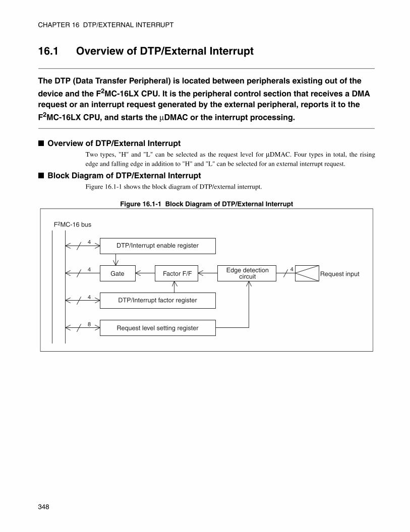
CHAPTER 16 DTP/EXTERNAL INTERRUPT
16.1 Overview of DTP/External Interrupt
The DTP (Data Transfer Peripheral) is located between peripherals existing out of the
device and the F2MC-16LX CPU. It is the peripheral control section that receives a DMA request or an interrupt request generated by the external peripheral, reports it to the
F2MC-16LX CPU, and starts the µDMAC or the interrupt processing.
Overview of DTP/External InterruptTwo types, "H" and "L" can be selected as the request level for µDMAC. Four types in total, the rising
edge and falling edge in addition to "H" and "L" can be selected for an external interrupt request.
Block Diagram of DTP/External InterruptFigure 16.1-1 shows the block diagram of DTP/external interrupt.
Figure 16.1-1 Block Diagram of DTP/External Interrupt
Request inputEdge detection
circuitFactor F/FGate
DTP/Interrupt enable register
DTP/Interrupt factor register
Request level setting register
F2MC-16 bus
4
4
4
8
4
348

CHAPTER 16 DTP/EXTERNAL INTERRUPT
16.2 Register of DTP/External Interrupt
This section describes the configuration and functions of registers used for the DTP and external interrupts.
Register List of DTP/External InterruptFigure 16.2-1 shows the register list of the DTP/external interrupts.
Figure 16.2-1 Register List of DTP/external Interrupt
DTP/Interruption Permission Register (ENIR: Enable Interrupt Request Register)Figure 16.2-2 shows the bit configuration of the DTP and enable interrupt register (ENIR).
Figure 16.2-2 Bit Configuration of the DTP and the Enable Interrupt Request Register (ENIR)
The DTP and the enable interrupt register (ENIR) determine to issue the request to the interrupt controller
by using the device terminal as the external interrupt and the DTP request input. The terminal
corresponding to the bits set to "1" in the ENIR register is used to input an external interrupt or DTP
request to issue the requests to the interrupt controller. The terminal corresponding to the bits set to "0"
holds the external interrupt or DTP request input factor but issues no request to the interrupt controller.
Address : 00003FH
Address : 00003EH
Address : 00003DH
Address : 00003CH
bit
bit
bit
bitDTP/Interrupt register (ENIR)
DTP/Interrupt register (EIRR)
Request level setting register (ELVR)
Request level setting register (ELVR)
7 6 5 4 3 2 1 0
15 14 13 12 11 10 9 8
7 6 5 4 3 2 1 0
15 14 13 12 11 10 9 8
EN7 EN6 EN5 EN4 EN3 EN2 EN1 EN0
ER7 ER6 ER5 ER4 ER3 ER2 ER1 ER0
LB3 LA3 LB2 LA2 LB1 LA1 LB0 LA0
LB7 LA7 LB6 LA6 LB5 LA5 LB4 LA4
Initial value
Address : 00003CH
7 6 5 4 3 2 1 0EN7 EN6 EN5 EN4 EN3 EN2 EN1 EN0
ENIR
00000000B
R/W R/W R/W R/W R/W R/WR/WR/W
349

CHAPTER 16 DTP/EXTERNAL INTERRUPT
DTP/Interruption Factor Register (EIRR: External Interrupt Request Register)Figure 16.2-3 shows the bit configuration of DTP/interruption factor register (EIRR).
Figure 16.2-3 Bit Configuration of DTP/interruption Factor Register (EIRR)
The DTP/interrupt factor register (EIRR) indicates the presence of corresponding external DTP/interrupt
request when reading and clears the flip-flop contents that indicates this request when writing. When "1" is
read from the EIRR register it indicates the external DTP/interrupt request presence in a terminal
corresponding to the ERx bit. In addition, when "0" is written in the EIRR register, the request flip-flop of
the corresponding bit is cleared. Writing "1" causes no operation. "1" is read with a read-modify-write
instruction.
Notes:
• The initial value is "00H" while the value is changed after the reset depending on the status ofterminal in the common-use with the external interrupt.
• Clear only the bits that the CPU accepted the interrupt (those bits that ER7 to ER0 are set to "1")to "0" when plural external interrupt request outputs are enabled (ENIR: EN7 to EN0 = 1). Noother bits must be cleared unconditionally.
• The value of the DTP/external interrupt factor bit (EIRR:ER) is available only when the corresponding DTP/external internal enable bit (ENIR:EN) is set to "1".When the DTP/external interrupt is not enabled (ENIR:EN = 0), the DTP/external interrupt may beset regardless of whether the DTP/external interrupt factor exists or not.
• Clear the corresponding DTP/external internal factor bit (ENIR:ER) just before enabling the DTP/external interrupts (ENIR:EN = 1).
Request Level Setting Register (ELVR: External Level Register) Figure 16.2-4 shows the bit configuration of the request level setting register (ELVR).
Figure 16.2-4 Request Level Setting Register (ELVR)
The request level setting register (ELVR) selects the request detection level. Two bits are allocated per
terminal as shown in Table 16.2-1. When the request input is in the level mode and the input is active, it is
again set even if it is cleared.
Initial value
(However, the object is different between both of them.)
Address : 00003DH
15 14 13 12 11 10 9 8ER7 ER6 ER5 ER4 ER3 ER2 ER1 ER0
EIRR00000000B
R/W R/W R/W R/W R/W R/WR/WR/W
Address : 00003FH
Address : 00003EH
7 6 5 4 3 2 1 0
15 14 13 12 11 10 9 8
LB3 LA3 LB2 LA2 LB1 LA1 LB0 LA0
LB7 LA7 LB6 LA6 LB5 LA5 LB4 LA4
ELVRInitial value00000000B
Initial value00000000B
R/W R/W R/W R/W R/W R/W R/W R/W
R/W R/W R/W R/W R/W R/W R/W R/W
350

CHAPTER 16 DTP/EXTERNAL INTERRUPT
Table 16.2-1 ELVR allocation (LA0-LA7,LB0-LB7)
LBx LAx Operation
0 0 There is a demand at "L" level.
0 1 There is a demand at "H" level.
1 0 Request present at the rising edge
1 1 Request present at the falling edge
351

CHAPTER 16 DTP/EXTERNAL INTERRUPT
16.3 Operation of DTP/External Interrupt
This section describes the Operation of DTP/External Interrupt.
External Interrupt OperationIf a request set by the ELVR register at the corresponding terminal is input after setting an external
interrupt request, this resource issues an interrupt request signal for the interrupt controller. When the
interrupt from this resource had the highest priority as a result of the priority identification of the interrupts
simultaneously occurred in the interrupt controller, the interrupt controller issues an interrupt request to the
F2MC-16LX CPU. The F2MC-16LX CPU compares the interrupt level mask register (ILM) in the
processor status (PS) with the interrupt request. When the request level is higher than the ILM bit, the
hardware interrupt process microprogram is started as soon as the current instruction execution is
terminated.
Figure 16.3-1 shows the external interrupt operation flow.
Figure 16.3-1 External Interrupt Operation
The interrupt process microprogram reads the interrupt vector area, issues the interrupt acknowledge to the
interrupt controller, transfers the macro instruction jump address generated by the vector to the program
counter, and executes the user interrupt process program.
Operation of DTPAs an initialization in the user program before starting the µDMAC, the register addresses allocated in from
000000H to 0000FFH are set to the I/O address pointer in the µDMAC descriptor and the memory buffer
start address is set to the buffer address pointer.
The DTP operation sequence is almost same with those of external interrupt and are quite identical until the
CPU starts the hardware interrupt process microprogram. When the µDMAC is started, the read or write
signal is sent to the addressed external peripheral device for the transfer operation with this chip. The
external peripheral device must cancel the interrupt request to this chip within three machine cycles after
the transfer operation. When the transfer is terminated, the descriptor, etc. are updated and the interrupt
controller generates the signal to clear the transfer factor. When this resource receives the signal to clear the
transfer factor, it clears the flip-flop that holds the factor and prepares for the next terminal request.
Figure 16.3-2 shows the timing to cancel the external interrupt request at the DTP operation termination.
In addition, Figure 16.3-3 shows the example of interfaces with external peripheral devices.
Interrupt controllerExternal interrupt/DTPOther requests
Factor
ELVR
EIRR
ENIR
ICRyy
ICRxx
CMP
IL
ILM
CMP
INTA
F2MC-16LXCPU
352

CHAPTER 16 DTP/EXTERNAL INTERRUPT
Figure 16.3-2 Timing to Cancel the External Interrupt Request at the DTP Operation Termination
Figure 16.3-3 Example of an External Peripheral Interface
Interrupt factor
Internal operation
Address bus pin
Data bus pin
Read signal
Write signal
Descriptorselect/read
Edge request or H level request
I/O register At memory transfer
Read address Write address
Read data Write data
Withdraw within 3-machine cycle.
Note : µDMAC
Internal busData, Address, Bus
Reg
iste
r
When transfer is terminated, withdraw within 3-machine cycle
IRQ DTP CORE MEMORY
MB90335
INT
Ext
erna
lpe
riphe
ral d
evic
e
353

CHAPTER 16 DTP/EXTERNAL INTERRUPT
16.4 Precaution of Using DTP/External Interrupt
Notes DTP/an external interruption is used are explained.
Condition of Peripheral Equipment Connected OutsideThe external peripheral device that the DTP can support must automatically clear the request at the transfer
execution. In addition, if the transfer request is not canceled within three-machine-cycle (an interim value)
after the transfer operation started, this resource handles it as if the next transfer request occurs.
Operation Process of DTP/External InterruptSet the registers within the DTP/external interrupt by using the following procedures:
1. The general-purpose I/O port that shared with the pin used as an external interruption input is set to the
Input port.
2. Disable the bits for the enable register.
3. The target bit for request level set register is set.
4. The target bit for the factor register is cleared.
5. Enable the bits for the enable register.
Simultaneous writing is possible for (4) and (5) with the word specification.
Before setting registers in this resource, the enable register must be disabled. In addition, before enabling
the enable register, the factor register must be cleared. These actions prevent erroneous interrupt factor
occurrence at register setting or in the interrupt enable state.
External Interrupt Request Level• Minimum 3 machine cycles are necessary for the pulse width to detect the edge presence when the
request level is set to the edge request.
• When the request input level is set to the level setting, the request to the interrupt controller remains
active while the interrupt request is enable (ENIR: EN = 1) even if an external request is input and
canceled afterward. To cancel the request for the interrupt controller, the interrupt request flag bit
(EIRR: ER) must be cleared.
Figure 16.4-1 Clearing the Interrupt Request Flag Bit (EIRR: ER) Upon Level Set
Interrupt factor Level detection The interrupt request flag bit (EIRR : ER) Enable gate
toInterrupt controller
Continue to retain the factor as long as it is not cleared.
354

CHAPTER 16 DTP/EXTERNAL INTERRUPT
Figure 16.4-2 Interrupt Factor when Enabling the Interrupt and the Interrupt Request for the Interrupt Controller
Interrupt factor(At detecting "H" level)
Interrupt request to interrupt controller
Inactive by clearing interrupt request flag bit (EIRR : ER)
Cancel the interrupt request
355

CHAPTER 16 DTP/EXTERNAL INTERRUPT
356

CHAPTER 17EXTENDED I/O SERIAL
INTERFACE
This chapter describes an overview of the extended I/O serial interface, the configuration and function of registers, and operations of extended I/O serial interface.
17.1 Outline of Extended I/O Serial Interface
17.2 Register in Extended I/O Serial Interface
17.3 Operation of Extended I/O Serial Interface
357

CHAPTER 17 EXTENDED I/O SERIAL INTERFACE
17.1 Outline of Extended I/O Serial Interface
The extended I/O serial interface is a serial I/O interface that can transfer data through the adoption of 8-bit x 1 channel configured clock synchronization scheme. LSB first/MSB first can be selected in data transfer.
Outline of Extended I/O Serial Interface The following two operation modes are available for the extended I/O serial interface.
• Internal shift clock mode: Transfers data in sync with the internal clock.
• External shift clock mode: Transfers data in sync with the clock input through an external pin (SCK).
In this mode, transfer operation performed by the CPU instruction is also
available by operating the general-use port sharing an external pin (SCK).
Block Diagram in Extended I/O Serial InterfaceFigure 17.1-1 shows the block diagram of extended I/O serial interface.
Figure 17.1-1 Block Diagram of Extended I/O Serial Interface
Internal data bus
Internal data bus
Initial value
ReadWrite
Transfer direction selection
SDR (Serial data register)
Shift clock counterControl circuit
Internal clock
Interruptrequest#38
(MSB first) D0 to D7
SIN
SOT
SCK
D7 to D0 (LSB first)
2 1 0
SMD2 SMD1 SMD0 SIE SIR BUSY STOP STRT MODE BDS SOE SCOE
SMCS
358

CHAPTER 17 EXTENDED I/O SERIAL INTERFACE
17.2 Register in Extended I/O Serial Interface
The configuration and functions of registers used in the extended I/O serial interface are described.
List of Register in Extended I/O Serial InterfaceFigure 17.2-1 shows the list of register in extended I/O serial interface.
Figure 17.2-1 List of Register in Extended I/O Serial Interface
Address
Address
Address
Address
R/W : Readable/Writable : Undefined
X : Indeterminate
Serial mode controlstatus register (SMCS) Initial value
Serial mode controlstatus register (SMCS)
Serial data register (SDR)
Initial value
Initial value
Initial value
Communication prescalercontrol register (SDCR)
SMCS: 000059H
SMCS: 000058H
SDR: 00005AH
SDCR: 00005BH
15 14 13 12 11 10 9 8
7 6 5 4 3 2 1 0
7 6 5 4 3 2 1 0
15 14 13 12 11 10 9 8
(R/W) (R/W) (R/W) (R/W) (R/W) (R) (R/W) (R/W)
(R/W) (R/W) (R/W) (R/W)
(R/W) (R/W) (R/W) (R/W) (R/W) (R/W) (R/W) (R/W)
(R/W) (R/W) (R/W) (R/W)(R/W)
SMD2 SMD1 SMD0 SIE SIR BUSY STRTSTOP
MODE BDS SOE SCOE
D7 D6 D5 D4 D3 D2 D1 D0
DIV3 DIV2 DIV1 DIV0MD
00000010B
XXXX0000B
XXXXXXXXB
0XXX0000B
359

CHAPTER 17 EXTENDED I/O SERIAL INTERFACE
17.2.1 Serial Mode Control Status Register (SMCS)
The configuration and functions of Serial mode control status register (SMCS) is described.
Serial Mode Control Status Register (SMCS)Serial mode control status register (SMCS) is a register which controls the transfer operating mode of serial
I/O.
Figure 17.2-2 shows the bit configuration of serial mode control status register (SMCS).
Figure 17.2-2 Bit Configuration of Serial Mode Control Status Register (SMCS)
Function of each bit of serial mode control status register (SMCS) is described as follows:
[bit15 to bit13] SMD2,SMD1,SMD0:Serial Shift Clock Mode (shift clock selection)
The serial shift clock mode is selected.
Table 17.2-1 and Table 17.2-2 show the settings of the serial shift clock mode.
Serial mode controlstatus registerInitial value
Serial mode controlstatus registerInitial value
Address
Address
SMCS: 000059H
SMCS: 000058H
R/W : Readable/Writable : Undefined
00000010B
XXXX0000B
SMD2 SMD1 SMD0 SIE SIR BUSY STRTSTOP15 14 13 12 11 10 9 8
(R/W) (R/W) (R/W) (R/W) (R/W) (R) (R/W) (R/W)
(R/W) (R/W) (R/W) (R/W)
7 6 5 4 3 2 1 0MODE BDS SOE SCOE
X : Indeterminate
Table 17.2-1 Serial Shift Clock Mode Selection
SMD2 SMD1 SMD0 φ=24 MHz
div=8 φ=12 MHz
div=4 φ=6 MHz
div=6 Value of dividing
frequency
0 0 0 1.5 MHz 1.5 MHz 500 kHz 2
0 0 1 750 kHz 750 kHz 250 kHz 4
0 1 0 188 kHz 188 kHz 62.5 kHz 16
0 1 1 93.4 kHz 93.4 kHz 31.2 kHz 32
1 0 0 46.9 kHz 46.9 kHz 15.6 kHz 64
1 0 1 External shift clock mode
1 1 0 Setting disabled
1 1 1 Setting disabled
360

CHAPTER 17 EXTENDED I/O SERIAL INTERFACE
Initialized to "000B" by reset. Rewriting under forwarding is a interdiction.
Shift clock includes five alternatives of internal shift clock and one alternative of external shift clock. The
external shifts. Please set neither "110B" nor "111B" to SMD2, SMD1, and SMD0.
Providing shift operation for each instruction is also possible by defining SCOE=0 on clock selection and
operating the port sharing SCK pin.
[bit12] SIE: Serial I/0 Interrupt Enable (enabling serial I/O interrupt)
Serial I/O interrupt request is controlled as shown in the table below.
• This bit is initialized to "0" at reset.
• This bit can be read and written.
[bit11] SIR: Serial I/0 Interrupt Request (serial I/O interrupt request)
On completion of the serial data transfer, this bit is set to "1". And when this bit turns to "1" on interrupt
enabled (SIE= 1), an interrupt request to the CPU occurs. A clear condition is different according to the
MODE bit.
• When MODE bit is "0", it is cleared by writing "0" to SIR bit.
• When MODE bit is "1", it is cleared by writing to or reading SDR bit.
• Regardless of values of MODE bit, it is cleared by resetting or writing "1" to STOP bit.
• It is not significant to write "1".
• On reading read/modify/write instructions, "1" is read in all cases.
[bit10] BUSY (forwarding status display)
This bit indicates whether serial transfer is running or not.
• This bit is initialized to "0" at reset.
• This bit can only be read.
Table 17.2-2 Example of Settings of the Communication Prescaler (SDCR)
Div (Machine clock) Machine cycle
(Recommended Setting)MD DIV3 DIV2 DIV1 DIV0
1 1 0 0 0 0 3 MHz
2 1 0 0 0 1 6 MHz
4 1 0 0 1 1 12 MHz
8 1 0 1 1 1 24 MHz
SIE Operation
0 Interrupt disabled [Initial value]
1 Serial I/O interrupt enabled
BUSY Operation
0 Stop or serial data register R/W standby [Initial value]
1 State of serial transfer
361

CHAPTER 17 EXTENDED I/O SERIAL INTERFACE
[bit9] STOP (stop bit)
This bit forcibly suspends serial transfer. When this bit is "1", the state changes into HALT based on
STOP=1.
• This bit is initialized to "0" at reset.
• This bit can be read and written.
[bit8] STRT: Start (start bit)
It is a bit by which the serial transfer is started. Forwarding is begun by writing "1" in the stopped state.
Lines specified as "1" are ignored, where serial transfer operation is on-going and the state is in serial
shift register R/W WAIT.
• Writing "0" is not significant.
• The bit always returns "0" when read.
[bit7 to bit4] Undefined bit
The read value is irregular. Nothing is affected when it is written.
[bit3] MODE (serial mode selection)
The startup condition from the stopped state is selected. However, rewriting under the operation is a
interdiction.
• This bit is initialized to "0" at reset.
• This bit can be read and written.
• This bit set to "1" at µDMAC start.
STOP Operation
0 Normal Operation
1 Forwarding stop [Initial value] by STOP=1
MODE Operation
0 Started when STRT = 1. [Initial value]
1 Started by reading or writing the serial data register.
362

CHAPTER 17 EXTENDED I/O SERIAL INTERFACE
[bit2] BDS: Bit Direction Selection (transfer direction selection)
On input and output of the serial data, Select either of the following alternatives: transfer in ascending
order from the least significant bit (LSB first); transfer in descending order from the most significant bit
(MSB first).
• This bit is initialized to "0" at reset.
• This bit can be read and written.
Note:
Select transfer direction before writing data to SDR.
[bit1] SOE: Serial Out Enable (serial output permission)
Controls the external pin (SOT) for serial I/O.
• This bit is initialized to "0" at reset.
• This bit can be read and written.
[bit0] SCOE: SCk1 Output Enable (shift clock output enable)
Controls output of the input/output external pins (SCK1,SCK2) for shift clock.
Set this bit to "0", when you transfer data in external shift clock mode for each individual instruction.
• Initialized to "0" at reset.
• This bit can be read and written.
BDS Operation
0 LSB first [Initial value]
1 MSB first
SOE Operation
0 General-purpose port [Initial value]
1 Serial data output
SCOE Operation
0 At the transfer by general-purpose port terminal and instruction [Initial value]
1 Shift clock output pin
363

CHAPTER 17 EXTENDED I/O SERIAL INTERFACE
17.2.2 Serial Data Register (SDR)
The configuration and functions of Serial data register (SDR) are described.
Serial Data Register (SDR)Figure 17.2-3 shows the bit configuration of the serial data register (SDR).
Figure 17.2-3 Bit Configuration of Serial Data Register (SDR)
The serial data register (SDR) is a serial data register to hold transfer data of the serial I/O.
Both writing and reading to and from SDR during transfer are disabled.
Serial data register
Initial value
7 6 5 4 3 2 1 0
(R/W) (R/W) (R/W) (R/W) (R/W) (R/W) (R/W) (R/W)
D7 D6 D5 D4 D3 D2 D1 D0AddressSDR
: 00005AH
R/W : Readable/Writable X : Indeterminate
XXXXXXXXB
364

CHAPTER 17 EXTENDED I/O SERIAL INTERFACE
17.2.3 Communication Prescaler Control Register (SDCR)
The configuration and functions of communication prescaler control register (SDCR) are described.
Communication Prescaler Control Register (SDCR) Figure 17.2-4 shows the bit configuration of communication prescaler control register (SDCR).
Figure 17.2-4 Communication Prescaler Control Register (SDCR)
The functions of each bit of the communication prescaler control register (SDCR) are described below.
[bit15] MD: Machine clock divide moDe select
Bit to enable the operation of the communication prescaler
[bit11 to bit8] DIV3,DIV2,DIV1,DIV0:DIVide3 to DIVide0
These bits determine the machine clock division ratio.
Initial value
Communication prescalercontrol registerAddress
SDCR: 00005BH
R/W : Readable/Writable : Undefined
15 14 13 12 11 10 9 8
(R/W) (R/W) (R/W) (R/W)(R/W)
DIV3 DIV2 DIV1 DIV0MD
0XXX0000B
X : Indeterminate
MD Operation
0 Communication Prescaler stops.
1 Communication Prescaler is operating.
DIV3 to DIV0 Rate of division
0000B 1-frequency division
0001B 2-frequency division
0010B 3-frequency division
0011B 4-frequency division
0100B 5-frequency division
0101B 6-frequency division
0110B 7-frequency division
0111B 8-frequency division
365

CHAPTER 17 EXTENDED I/O SERIAL INTERFACE
Note:
In the case of making changes to the rate of division, allow for two divisions of intervals as theduration of stabilization of the clock before communication.
366

CHAPTER 17 EXTENDED I/O SERIAL INTERFACE
17.3 Operation of Extended I/O Serial Interface
Extended I/O interface consists of a serial mode control status register (SMCS) and a serial data register (SDR) and is used to input and output 8-bit serial data.Operation of extended I/O serial interface is described.
Outline of Operation of Extended I/O Serial InterfaceWhen serial data is input or output, each of input and output operations is performed as described below.
Input of Serial data
The content of the serial data register is output in a bit serial fashion to the serial output pin (SOT pin) in
synchronization with the falling edge of the serial shift clock (external clock, internal clock).
Output of Serial data
Input from the serial input pin (SIN pin) into SDR (serial data register) in a bit serial fashion in
synchronization with the rising edge of the serial shift clock (external clock, internal clock).
The direction of shift (transfer from MSB or LSB) can be specified by the bit of direction specification
(BDS) of SMCS (serial mode control status register).
Once the transfer completes, the state goes into STOP or into data register R/W wait (or SDR R/W WAIT)
by MODE bit of the serial mode control status register (SMCS). To change state into TRANSFER from
each of the states, you should do each of the following steps.
• To return from HALT, write "0" in STOP bit, and "1" in STRT bit (STOP and STRT can be set
concurrently).
• To return from serial data register R/W wait (SDR R/W WAIT), read or write the data register.
367

CHAPTER 17 EXTENDED I/O SERIAL INTERFACE
17.3.1 Shift Clock Mode
Shift clock includes two types of modes; one is Internal Shift Clock Mode, the other is External Shift Clock Mode, both of which are specified by settings of SMCS. Please switch the mode with serial I/O stopped. Reading BUSY bit allows the checking of the state of HALT.
Internal Shift Clock ModeOperation is driven by the internal clock, and the shift clock whose duty ratio is 50% is output from SCK
pin as an output of the timing of synchronization.
Data is forwarded by one bit per a clock.
Transfer rate can be calculated using the following formula.
A indicates the rate of division represented by SMD bit of SMCS.
(φ/div)/2, (φ/div)/22, (φ/div)/24, (φ/div)/25, (φ/div)/26
External Shift Clock ModeIn synchronization with the external shift clock input through SCK pin, 1 bit of data is transferred for each
individual clock.
Allowed transfer rate varies from DC to 1/(8 machine cycles). When 1 machine cycle = 62.5 ns for
example, a maximum of 2 MHz is allowable.
Transfer by instruction by instruction can be accomplished by setting as described below.
• Select the external shift clock mode, and set SCOE bit of SMCS to "0".
• Write "1" in the direction register of which the port shares SCK pin, and place the port in the output
mode.
Once the settings complete as indicated above, write "1" or "0" in the data register (PDR) of the port, then
the value to be delivered to SCK pin is captured as the external clock and transfer operation is
accomplished. Have the shift clock start at "H".
Note:
Writing to SMCS.SDR during serial I/O operation is disabled.
transfer rate (s)Internal clock machine cycle (A)
A=
368

CHAPTER 17 EXTENDED I/O SERIAL INTERFACE
17.3.2 Operation State of Serial I/O
The states of serial I/O operation includes the following 4 types of states; STOP, HALT, R/W WAIT of SDR, and TRANSFER.
Operation State of Serial I/O
STOP State
On RESET or in the state of writing "1" in STOP bit of SMCS, the shift counter is initialized, resulting in
SIR=0.
Returning from the stop state is performed by setting STOP = 0 and STRT = 1 (both can be set at the same
time). Even though STRT=1 is provided when STOP=1, transfer operation is not executed, since STOP bit
is upper than STRT bit.
HALT State
When MODE bit is "0", termination of transfer provides SMCS with BUSY=0 and SIR=1, resulting in the
initialization of the counter to go into HALT state. To return from the HALT state, set STRT to "1", then
transfer operation restarts.
Serial data register R/W standby
When MODE bit of SMCS is "1", termination of serial transfer provides SMCS with BUSY=0 and SIR=1,
resulting in the serial data register to go into R/W WAIT state. If the interrupt enable register is enabled,
this block issues interrupt signals.
To return from the R/W WAIT state, when the serial data register is read or written, then BUSY is set to
"1", which allows to transfer operation to restart.
369

CHAPTER 17 EXTENDED I/O SERIAL INTERFACE
Transfer State
It is a state to do the serial transfer by BUSY = 1. MODE bit triggers the transition to the state of HALT
and R/W WAIT respectively.
Figure 17.3-1 shows the transition diagram of each state, and Figure 17.3-2 shows the conceptual diagram
of read/write of the serial data register.
Figure 17.3-1 Transition Diagram of Operation in Extended I/O Serial Interface
Figure 17.3-2 Conceptual Diagram of Reading/writing Serial Data Register
(1)When MODE=1, transfer is terminated by the shift clock counter. This allows SIR=1 to go into read/
write state. If the SIE bit is "1", the interruption signal is generated. However, when SIE is inactive, or
when writing "1" in STOP causes the suspend of transfer, interrupt signals are not generated.
(2)Once the serial data register is read or written, interrupt requests are cleared, and serial transfer starts.
Reset
Stop state (Transfer complete)
Transfer operation Serial data register R/wait
STRT=0, BUSY=0MODE=0 STRT=0, BUSY=0
STOP
MODE=0&
STOP=0&
END
STOP=0&
STRT=1
STOP=0 & STRT=0
STOP=1
STOP=1STOP=0
STRT=1& STOP=1
MODE=1 & END & STOP=1
SDR R/W & MODE=1STRT=1, BUSY=1 STRT=1, BUSY=0
MODE=1
Data bus
Data busInterrupt input Interrupt
controller
ReadWrite
Data bus
Interrupt output
ReadWriteS
eria
l dat
a
Extended I/O serial interface
CPU
SOT
SIN
(1)
(2)
370

CHAPTER 17 EXTENDED I/O SERIAL INTERFACE
17.3.3 Start/Stop Timing of Shift Operation and Timing of I/O
Start/stop timing of shift operation and timing of I/O is described.
Start/stop Timing of Shift Operation and Timing of I/O• Start
STOP bit of Start SMCS is set to "0", while STRT bit to "1".
• Stop
One halt is triggered from the termination of transfer; the other from STOP=1.
- Halt from STOP=1: Halts staying with SIR=0, regardless of MODE bit.
- Halt from transfer termination: Halts with SIR=1, regardless of MODE bit.
Regardless of MODE bit when BUSY bit is in the state of serial transfer, it is set to "1", and when in HALT
or R/W WAIT state, it is set to "0". Please read this bit to confirm forwarding.
The following chart shows the operation for each mode and the timing of halt operation. D07 to D00 in
figure shows output data.
Internal shift clock mode (LSB first)
Figure 17.3-3 Start/stop Timing of Shift Operation (Internal Clock)
External shift clock mode (LSB first)
Figure 17.3-4 Start/stop Timing of Shift Operation (External Clock)
(Transfer complete)(Transfer start)
(Data hold)
SCK
STRT
BUSY
SOT
MODE=0
D00 D07
"1" Output
(Transfer complete)(Transfer start)
(Data hold)
SCK
STRT
BUSY
SOT
MODE=0
D00 D07
371

CHAPTER 17 EXTENDED I/O SERIAL INTERFACE
For instruction shift in external shift clock mode (LSB first)
In instruction shift, when "1" is written to the bit corresponding to SCK of PDR, "H" is output, and when
"0" is written, "L" is output (where external shift clock mode is selected, and SCOE=0).
Figure 17.3-5 When Instruction Shift is Performed in the External Shift Clock Mode.
Stop by STOP=1 (LSB first, At internal clock)
Figure 17.3-6 Stop Timing when STOP Bit is Assumed to be "1"
Operation during Transfer Serial DataDuring transferring serial data, data from the serial output terminal (SOT) is output on the falling edge of
the shift clock, data of the serial input terminal (SIN) is input on the rising edge.
LSB first (when BDS bit is set to "0")
Figure 17.3-7 Shift Timing of I/O (LSB First)
MSB first (when BDS bit is set to "1")
Figure 17.3-8 Shift Timing of I/O (LSB First)
SCK bit "0" of PDR SCK bit "0" of PDR
When Mode = 0
SCK bit "1" of PDR (Transfer end)
(Data hold)
SCK
STRT
BUSY
SOT D06 D07
(Transfer complete)(Transfer start)
(Data hold)
"1" OutputSCK
STRT
BUSY
SOT
STOP
D03 D04
MODE=0
D05
SIN Input
SOT Output
SCK
SIN
SOT
DI0 DI1 DI2 DI3 DI4 DI5 DI6 DI7
DO0 DO1 DO2 DO3 DO4 DO5 DO6 DO7
SIN Input
SOT Output
SCK
SIN
SOT
DI7 DI6 DI5 DI4 DI3 DI2 DI1 DI0
DO7 DO6 DO5 DO4 DO3 DO2 DO1 DO0
372

CHAPTER 17 EXTENDED I/O SERIAL INTERFACE
17.3.4 Interrupt Function
Extended I/O serial interface can generate the interrupt request to the CPU.
Interruption Function of Extended I/O Serial InterfaceUpon completion of data transfer, SIR bit indicating an interrupt flag is set, and when SIE bit of the SMCS
enabling interrupts is "1", the interrupt request is output to the CPU.
Figure 17.3-9 shows the output timing of interrupt signal.
Figure 17.3-9 Output Timing of Interruption Signal
(Transfer complete)
(Data hold)
RD/WR of SDR
SCK
BUSY
SIR
SOT
SIE=1
MODE=1
DO6 DO7
373

CHAPTER 17 EXTENDED I/O SERIAL INTERFACE
374

CHAPTER 18UART
This chapter explains the function and operation of the UART.
18.1 Overview of UART
18.2 UART Block Diagram
18.3 UART Pins
18.4 Register of UART
18.5 UART Interrupt
18.6 UART Baud Rate
18.7 Explanation of Operation of UART
18.8 Notes on Using UART
18.9 Example of UART Programming
375

CHAPTER 18 UART
18.1 Overview of UART
UART is a general purpose serial data communication interface for synchronous or asynchronous (start-stop synchronization) communications with external devices. Not only the typical function of bidirectional communication (normal mode), but also the function of master/slave communication (multiprocessor mode: only supported master side) are supported.
UART Function
UART function
UART, or a general serial data communication interface that sends and receives serial data to and from
other CPU and peripherals, has the functions listed in Table 18.1-1.
Note:
At clock synchronous transfer, data is transferred alone with neither start nor stop bit added.
Table 18.1-1 UART Function
Functions
Data buffer Full-duplicate double-buffer
Transfer mode• Clock synchronous (No start/stop bit)• Clock asynchronous (start-stop synchronization to clock)
Baud rate• Dedicate baud-rate generator• External clock input enabled.
Data length• 8 bits or 7 bits (in the asynchronous normal mode only)• 1 to 8 bit (s) (synchronous mode only)
Signal type NRZ (Non Return to Zero) type
Detection of receive error• Framing error• Overrun error• Parity error (Not supported in operation mode 1)
Interrupt request
• Receive interrupt (receive, detection of receive error)• Transmission interrupt (transmission complete)• Support extended intelligent I/O service (EI2OS) and µDMAC transfer for both
transmission and receive
Master/slave type communication function (multi processor mode)
Capable of 1 (master) to n (slaves) communication(available just as master)
376

CHAPTER 18 UART
Table 18.1-2 UART Operation Modes
Operating mode
Data lengthSynchronous
typeLength of Stop BitWithout
ParityWith Parity
0 Normal mode 7 bits or 8 bits Asynchronous 1 bitor
2 bits *21 Multiprocessor mode 8 bit + 1 *1 - Asynchronous
2 Normal mode 1 to 8 bits - Synchronous None
-: Unavailable*1: "+1" indicates the address/data select bit (A/D) used for communication control.*2: During reception, only one bit is detected as the stop bit.
377

CHAPTER 18 UART
18.2 UART Block Diagram
UART is composed of the following block.
UART Block Diagram
Figure 18.2-1 UART Block Diagram
Control bus
Pin
Pin
Pin
Start bitdetection circuit
Transmit startcircuit
Dedicated baudrate generator
Clo
ck s
elec
tor
Mac
hine
clo
ck Transfer clock
Receive interrupt signal
Receivecontrolcircuit
Transmitcontrolcircuit
Transmitinterrupt signal
Receive clock
SCK0, SCK1External clock
SIN0, SIN1
SOT0, SOT1
SODR0, SODR1SIDR0, SIDR1
UART prescalercontrol register(UTCR0, UTCR1)
UART prescalerreload register
Receive bitcounter
Transmit bitcounter
Receive paritycounter
Transmit paritycounter
Receiving shift register
Receive statejudge circuit
Transmit shift register
Receiving end Transmission
end
SMR0,SMR1register
SCR0,SCR1register
SSR0,SSR1register
(UTRLR0, UTRLR1)
PEOREFRERDRFTDREBDSRIETIE
PENPSBLCLA/DRECRXETXE
MD1MD0SCKLM2L2M2L1M2L0SCKESOE
F2MC - 16LX Bus
378
CHAPTER 18 UART
Clock selector
Dedicated baud rate generator, selecting the send and receive clock from external input clocks.
Reception Control Circuit
The reception control circuit is configured with the reception bit counter, start bit detecting circuit, and
reception parity counter. The receive bit counter counts receiving data. Once this counter completes
receiving a piece of data based on the specified data length, then a receiving interrupt request is generated.
The start bit detection circuit is a circuit that detects the start bit from serial input signals. When detecting
the start bit, this circuit writes the data in the serial input data registers 0, 1 (SIDR0, SIDR1) with shifting
based on specified transfer rates. The receive parity counter calculates parity in received data.
Transmission Control Circuit
The transmission control circuit is configured with the transmission bit counter, transmission start circuit,
and transmission parity counter. The send bit counter counts sending data. Once this counter completes
sending a piece of data based on the specified data length, then a sending interrupt request is generated. The
sending start circuit starts sending operation by writing to the serial output data registers 0, 1 (SODR0,
SODR1). The transmit parity counter generates a parity bit for data to be transmitted if the data is parity-
checked.
Receive shift register
This circuit captures the receiving data, shifting bit by bit, that is input from SIN0 to SIN3 pins. On
completion of reception, this circuit transfers the receiving data to the serial input data registers 0, 1
(SIDR0, SIDR1).
Transmit shift register
The data that is written to the serial output data registers 0, 1 (SODR0, SODR1) is transferred to the
sending shift register, which outputs it to the SOT pin with shifting bit by bit.
Serial mode register 0, 1 (SMR0, SMR1)
Specifies selecting operation modes, enabling/disabling output of serial data to the pin, setting to enable/
disable output of the clock to the pin, setting the arbitrary number of 1 bit to 8 bits to be transferred in the
synchronous communication mode, and setting levels of serial clock output (fixed on "L", fixed on "H")
when not operating.
Serial control register 0, 1 (SCR0, SCR1)
Specifies setting the presence or the absence of parity, selection of parity, setting stop bit length, setting
data length, selecting frame data format in the mode 1, clearance of flags, and enabling/disabling of sending
and receiving.
Serial Status Register 0, 1 (SSR0, SSR1)
Checking sending and receiving, or the states of errors, and specifies enabling/disabling sending and
receiving interrupt requests.
379

CHAPTER 18 UART
Serial input data register 0, 1 (SIDR0, SIDR1)
The register retains the receive data. The serial input is converted and then stored in this register.
Serial output data register 0, 1 (SODR0, SODR1)
The register sets the transmit data. Data written to this register is serially converted to be output.
UART prescaler control register 0, 1 (UTCR0, UTCR1)
Specifies start-up/halt of the communication prescaler, forced reset of UART, selecting of clock sources,
and the rate of division of the machine clock.
UART prescaler reload register 0, 1 (UTRLR0, UTCR1)
Specifies the division rate of the machine clock.
380
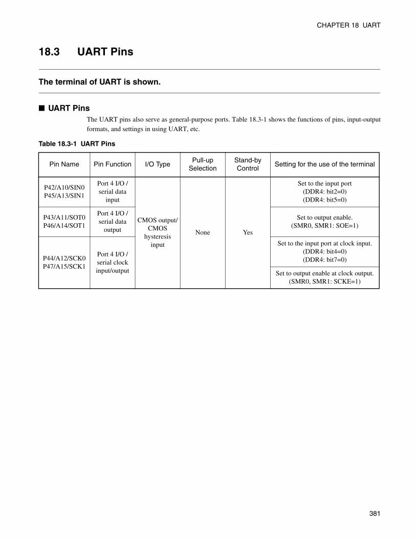
CHAPTER 18 UART
18.3 UART Pins
The terminal of UART is shown.
UART PinsThe UART pins also serve as general-purpose ports. Table 18.3-1 shows the functions of pins, input-output
formats, and settings in using UART, etc.
Table 18.3-1 UART Pins
Pin Name Pin Function I/O TypePull-up
SelectionStand-by Control
Setting for the use of the terminal
P42/A10/SIN0 P45/A13/SIN1
Port 4 I/O /serial data
input
CMOS output/CMOS
hysteresis input
None Yes
Set to the input port(DDR4: bit2=0) (DDR4: bit5=0)
P43/A11/SOT0 P46/A14/SOT1
Port 4 I/O /serial data
output
Set to output enable.(SMR0, SMR1: SOE=1)
P44/A12/SCK0 P47/A15/SCK1
Port 4 I/O /serial clockinput/output
Set to the input port at clock input.(DDR4: bit4=0) (DDR4: bit7=0)
Set to output enable at clock output.(SMR0, SMR1: SCKE=1)
381

CHAPTER 18 UART
18.4 Register of UART
The list of the register of UART is shown.
List of UART Register
Figure 18.4-1 List of UART Register
Note:
When you set the communication mode, do this while operation is halted. Any data sent or receivedwhile setting modes is not guaranteed.
Address
ch.0 : 000021H, 20H
ch.1 : 000027H, 26H
ch.0 : 000023H, 22H
ch.1 : 000029H, 28H
ch.0 : 000025H, 24H
ch.1 : 00002BH, 2AH
(Serial control register 0, 1)SCR0, SCR1
(Serial status register 0, 1)SSR0, SSR1
(UART prescaler control register 0, 1)UTCR0, UTCR1
(Serial mode register 0, 1)SMR0, SMR1
(Serial input · Output data register 0, 1)SIDR0, SIDR1 · SODR0, SODR1
(UART prescaler reload register 0, 1)UTRLR0, UTRLR1
bit8 bit7 bit0bit15
382

CHAPTER 18 UART
18.4.1 Serial Control Register 0, 1 (SCR0, SCR1)
Serial control registers 0, 1 (SCR0, SCR1) are responsible for setting parity, selecting the stop bit length and data length, selecting the frame data format in mode 1, clearing receiving error flags, and enabling/disabling send and receive operations.
Serial Control Register 0, 1 (SCR0, SCR1)
Figure 18.4-2 Serial Control Register 0, 1 (SCR0, SCR1)
Initial value
Bit indicating that sending operation
Bit indicating that receiving operation
Receiving error clear bit
Address/Data selection bit
Data length selection bit
Stop bit length selection bit
Parity selection bit
Parity enable bit
Sending operation disabled
Sending operation enabled
Receiving operation disabled
Receiving operation enabled
Clear FRE, ORE, PE flag.
Data frame
Address frame
7 bit
8 bit
1 bit length
2 bit length
Even parity
With Parity
No Parity
Odd parity
The conversion is not changed and no others are affected
R/W : Readable/Writable W: Write only
: Initial value
Only enable when parity is existent (PN = 1)
Addressch.0 : 000021H
ch.1 : 000027H
R/W R/W R/W R/W R/W W R/W R/W
bit15 bit14 bit13 bit12 bit11 bit10 bit9 bit8 bit7 bit0
00000100B(SMR0, SMR1)TXERXERECADCLSBLPEN P
TXE
0
1
0
1
RXE
REC
0
1
A/D
0
1
CL
0
1
SBL
0
1
P
0
1
PEN
0
1
383

CHAPTER 18 UART
Table 18.4-1 Functional Description of Each Bit in Serial Control Register 0, 1 (SCR0, SCR1)
Bit name Functions
bit15 PEN: Parity enable bits
• Specify whether to add (at sending) or detect (at receiving) a parity bit.Note: In operation mode1 and operation mode 2, parity bit cannot be appended. Always set
this bit to "0".
bit14 P: Parity selection bits
• Select either odd or even parity when the use of the parity bit has been selected (SCR0, SCR1: PEN = 1).
bit13 SBL:Stop bit length selection bits
• Set the length of the stop bits (transmit data’s frame end mark) in operation mode 0 and operation mode 1 (asynchronous).
Note: During receiving data, only the first bit of the stop bit is detected in all cases.
bit12 CL: Data length selection bits
• Specify the data length of data to be transmitted and received.It is only operation mode 0 to be able to select seven bits. In operation mode 1 and operation mode 2, be sure to set a data length of 8 bits.
bit11 AD: Address/data selection bits
• In operation mode 1, set the data format of frames to be transmitted/received.• When the bit is set to "0": The frame format is set to data frame.• When the bit is set to "1": The frame format is set to address data frame.
bit10 REC: Receive error flag clear bits
• Clear the reception error flags (SSR0, SSR1: FRE, ORE, PE) in the serial status register to "0".
• When the bit is set to "0": The FRE, ORE, and PE flags are cleared.• When the bit is set to "1": No effect.• When read: "1" is always read.Note: When the receiving interrupt is set to be enabled (SSR0, SSR1:RIE=1), REC bit
may be set to "0" as long as each of FRE, ORE, PE flag is set to "1".
bit9
RXE: Reception operation enable bits
• The bit enables or disables the UART for reception.• When the bit is set to "0": Reception is disabled.• When the bit is set to "1": Reception is enabled.Note: During receiving data, if the receiving operation is set to be disabled, the receiving
operation is halted after in-coming data is stored in the serial input data register.
bit8
TXE: Transmission operation enable bits
• The bit enables or disables the UART for transmission.• When the bit is set to "0": Transmission is disabled.• When the bit is set to "1": Transmission is enabled.Note: If transfer operation is set to be disabled during data transfer, the transfer operation is
stopped on completion of data transfer of the serial output data register.
384

CHAPTER 18 UART
18.4.2 Serial Mode Register 0, 1 (SMR0, SMR1)
The serial mode registers 0, 1 (SMR0, SMR1) are responsible for selecting operation modes, setting pins related to serial data and cock to be enabled or disabled, and setting how many bit to transfer ranging from 1 to 8 bits, setting the serial clock output level in the inactive operation (fixed to "L" and "H").
Serial Mode Register 0, 1 (SMR0, SMR1)
Figure 18.4-3 Serial Mode Register 0, 1 (SMR0, SMR1)
Initial value
Serial data output enable bit
Serial clock output enable bit
As general-purpose port
As Serial data output pin of UART
As Clock output pin of UART
Synchronous mode transfer number setting bit
Transfer number: 8 bit
Transfer number: 1 bit
Transfer number: 2 bit
Transfer number: 3 bit
Transfer number: 4 bit
Transfer number: 5 bit
Transfer number: 6 bit
Transfer number: 7 bit
As general-purpose port or Clock input pin of UART0/1
Serial clock output level setting bit
Operation mode selection bit
Operation mode
Asynchronous mode (Normal mode)
Synchronous mode (Normal mode)
Setting disabled
Asynchronous mode (multiprocessor mode)
Serial clock output "L" level when not operating
Serial clock output "H" level when not operating
: Readable/Writable: Initial value
Addressch.0 : 000020H
ch.1 : 000026H
bit7 bit6 bit5 bit4 bit3 bit2 bit1 bit0bit15 bit8
MD1 MD0 SCKL M2L2 M2L1 M2L0 SCKE SOE
R/W R/W R/W R/WR/W R/W R/W R/W
00100000B(SCR0, SCR1)
SOE
0
1
0
1
SCKE
M2L2 to M2L0
"000B"
"001B"
"010B"
"011B"
"100B"
"101B"
"110B"
"111B"
SCKL
0
1
MD1 MD0
0
0
0
0
1
1
11R/W
0
2
1
385

CHAPTER 18 UART
Table 18.4-2 Functional Description of Each Bit in Serial Mode Register 0, 1 (SMR0, SMR1)
Bit name Functions
bit7 bit6
MD1, MD0: Operating mode selection bits
• Set Operating modeNotes:- In operation mode 1, the device can be used only as the master for master/slave
communication. In operation mode 1, the address/data bit as bit9 cannot be received, so the device cannot be used as the slave.
- In operation mode 1, set the parity addition enable bit to no parity (SCR0, SCR1: PEN = 0) as the parity check function cannot be used.
bit5 SCKL: Serial clock output level set bit
• When communication is operated in the clock synchronous mode, serial clock output level is set to the non-operating level.
• When set to "0": Output of serial clock is "L" level.• When set to "1": Output of serial clock is "H" level.
bit4 bit3 bit2
M2L2, M2L1, M2L0: Synchronous mode transfer numerical set bits
• Specify the number of bits transferred in the synchronous communication mode.• It is invalid at the asynchronous communication mode.• When set to "000B": Specify as 8-bit transmission.• When set to "001B": Specify as 1-bit transmission.• When set to "010B": Specify as 2-bit transmission.• When set to "011B": Specify as 3-bit transmission.• When set to "100B": Specify as 4-bit transmission.• When set to "101B": Specify as 5-bit transmission.• When set to "110B": Specify as 6-bit transmission.• When set to "111B": Specify as 7-bit transmission.
bit1
SCKE: Serial Clock Input/Output enable bits
• Switch between input and output of the serial clock.• When the bit is set to "0":The pin is set as a general-purpose I/O port or serial clock input
pin.• When the bit is set to "1":The pin is set as a serial clock output pin.Notes:- When using the SCK0, SCK1 pin as the serial clock input (SCK=0), set the pin to the input
port using the port direction register (DDR). Also, use the clock input source select bit to select the external clock (UTCR0, UTCR1: CKS=1B).
- When using this as serial clock output, set the clock input source selection bit to the dedicated baud rate generator (UTCR0, UTCR1: CKS=0 B).
- When SCK pins (0, 1) are set to serial clock output, they function as serial clock output pins, regardless of the settings of the generic input-output port.
bit0 SOE: Serial data output enable bits
• Enable or disable output of serial data.• When the bit is set to "0": The pin is set as a general-purpose I/O port.• When the bit is set to "1": The pin is set as a serial data output pin.• When SOT pins (0, 1) are set to serial data output, they function as serial clock output pins,
regardless of the settings of the generic input-output port.
386

CHAPTER 18 UART
18.4.3 Serial Status Register 0, 1 (SSR0, SSR1)
The serial status registers 0, 1 (SSR0, SSR1) are responsible for checking sending and receiving and the states of errors, and setting interrupts to be enabled or disabled.
Serial Status Register 0, 1 (SSR0, SSR1)
Figure 18.4-4 Serial Status Register 0, 1 (SSR0, SSR1)
Initial value
Transfer interrupt request enable bit
Transfer interrupt request output enabled
Transfer interrupt request output disabled
Receive interrupt request enable bit
Transfer direction selection bit
Transfer data empty flag bit
Receive data full flag bit
No Receive data
With Receive data
With Transfer data (Transfer data writing disabled)
No Transfer data (Transfer data writing enabled)
Receive interrupt request output enabled
Receive interrupt request output disabled
MSB first (Transfer form Most significant bit)
LSB first (Transfer form Least significant bit)
Framing error flag bit
Over run error flag bit
Parity error flag bit
No Framing error
With Framing error
No Over run error
With Over run error
No Parity error
With Parity errorR/W : Readable/Writable
Addressch.0 : 000023H
ch.1 : 000029H
bit15 bit14 bit13 bit12 bit11 bit10 bit9 bit8 bit7 bit0
00001000BPE ORE FRE RDRF TDRE BDS RIE TIE (SIDR0, SIDR1, SODR0, SODR1)
TIE
0
1
RIE
0
1
BDS
0
1
TDRE
0
1
RDRF
0
1
FRE
0
1
ORE
0
1
PE
0
1R : Read only
: Initial value
R R/W R/W R/WR R R R
387

CHAPTER 18 UART
Table 18.4-3 Description of Each Bit of the Serial Status Registers 0, 1 (SSR0, SSR1) (1/2)
NO. Bit name Functions
bit15 PE: Parity error flag bit
• Detect a parity error of receiving data.• This bit is set to "1" when a parity error occurs.• This is cleared by writing "0" in the receiving error clear bit (SCR0, SCR1: REC).• When receiving interrupts are enabled (SCR0, SCR1: RIE=1), a receiving interrupt
request is generated if a parity error occurs• When the parity error flag bit is set (SSR0, SSR1: PE = 1), data in serial input data
register is invalid.
bit14 ORE: Overrun error flag bit
• Detect an overrun error in receiving.• This bit is set to "1" when an overrun error occurs.• This is cleared by writing "0" in the receiving error flag clear bit (SCR0, SCR1: REC).• When receiving interrupts are enabled (SSR0, SSR1: RIE=1), a receiving interrupt
request is generated if a overrun error occurs.• When the overrun error flag bit is set (SSR0, SSR1: ORE = 1), data in serial input data
register is invalid.
bit13 FRE: Framing error flag bit
• Detect a framing error of receive data.• This bit is set to "1" when a framing error occurs.• This is cleared by writing "0" in the receiving error clear bit (SCR0, SCR1: REC).• When receiving interrupts are enabled (SSR0, SSR1: RIE=1), a receiving interrupt
request is generated if a framing error occurs.• When the framing error flag bit is set (SSR: FRE = 1), data in serial input data register is
invalid.
bit12 RDRF: Receive Data full flag bit
• Show the status of the serial input data register.• When received data is loaded to serial input data register 0, 1 (SIDR0, SIDR1), "1" is set.• This bit is cleared to "0" when data is read from the serial input data register 0, 1 (SIDR0,
SIDR1).• When receiving interrupts are enabled (SSR0, SSR1: RIE=1), a receiving interrupt
request are generated if receiving data is loaded to the serial input data registers (SIDR0, SIDR1).
bit11 TDRE: Transmission data empty flag bit
• Show the status of the serial output data register 0, 1 (SODR0, SODR1).• The bit is cleared to "0" by writing sending data to the serial output data registers 0, 1
(SODR0, SODR1).• This bit is set to "1" when data is loaded to the send shift register and transmission starts.• When sending interrupts are enabled (SSR0, SSR1: TIE=1) and if the data that has
written to the serial output data registers 0, 1 (SODR0, SODR1) is transferred to the sending shift register, then a sending interrupt request is generated.
bit10 BDS: Transfer direction selection bit
• This bit sets the direction of serial data transfer.• When set to "0": Serial data is transferred from the LSB bit first (LSB first).• When set to "1": Serial data is transferred from the MSB bit first (MSB first).Note:
If BDS bit is rewritten after the completion of the access to the register, the rewritten data will be invalid, since in reading to the serial input data register and in writing to the serial output data register, the LSB data and the MSB data are turned upside down.
388

CHAPTER 18 UART
bit9
RIE: Reception interrupt request enable bits
• Enable or disable receive data.• When set to "1": If receiving data is loaded to the serial input data registers 0, 1 (SSR0
to SSR3: RDRF=1). Or if an receiving error occurs (SSR0, SSR1: PE=1, or ORE=1, or FRE=1), then a receiving interrupt request is
generated.
bit8
TIE: Transmission interrupt request enable bits
• Enable or disable send interrupt.• When set to "1": If the data written to the serial output data registers 0, 1 is sent to the
sending shift register (SSR0, SSR1: TDRE=1), then a sendinginterrupt request is generated.
Table 18.4-3 Description of Each Bit of the Serial Status Registers 0, 1 (SSR0, SSR1) (2/2)
NO. Bit name Functions
389

CHAPTER 18 UART
18.4.4 Serial Input Data Register 0, 1(SIDR0, SIDR1) and Serial Output Data Register0, 1(SODR0, SODR1)
Serial input data and serial output data registers are located in the same address. They function as a serial input data register in reading, while in writing as a serial output data register.
Serial Input Data Register 0, 1 (SIDR0, SIDR1) Figure 18.4-5 shows the bit configuration of the serial input data register.
Figure 18.4-5 Serial Input Data Register 0, 1 (SIDR0, SIDR1)
Serial input data register 0, 1 (SIDR0, SIDR1) is a data buffer register for receiving serial data.
• The serial data signals sent to the serial input pins (SIDR0, SIDR1) are converted in the shift register,and stored in the serial input data registers 0, 1 (SIDR0, SIDR1).
• When the data length is 7 bits, the upper one bit (SIDR0, SIDR1:D7) becomes invalid.
• When the receiving data is stored in the serial input data registers 0, 1 (SIDR0, SIDR1), the receivingdata full flag bit (SSR0, SSR1: RDRF) is set to "1". When receiving interrupts are enabled (SSR0,SSR1: RIE=1), receiving interrupt requests are generated.
• Read the serial input data registers 0, 1 (SIDR0, SIDR1) in the state that the receiving data full flag bit(SSR0, SSR1: RDRF) is set to "1". When the receiving data full flag bit (SSR0, SSR1: RDRF) reads theserial input data registers 0, 1 (SIDR0, SIDR1), it is automatically cleared to "0".
• If any receiving error occurs (SSR0, SSR1: PE, ORE, or FRE is "1"), the data of the serial input dataregisters 0, 1 (SIDR0, SIDR1) is invalid.
Initial value
R : Read onlyX : Indeterminate
bit7 bit6 bit5 bit4 bit3 bit2 bit1 bit0Addressch.0 : 000022H
ch.1 : 000028H
R R R R R R R R
XXXXXXXXBD7 D6 D5 D4 D3 D2 D1 D0
390

CHAPTER 18 UART
Serial Output Data Register 0, 1 (SODR0, SODR1) Figure 18.4-6 shows the bit configuration of serial output data register.
Figure 18.4-6 Serial Output Data Register 0, 1 (SODR0, SODR1)
The serial output data register 0, 1 (SODR0, SODR1) is a data buffer register for transmitting serial data.
• When sending operation is allowed (SCR0, SCR1: TXE=1), and if the sending data is written to theserial output data registers 0, 1 (SODR0, SODR1), the sending data is transferred to the sending shiftregister to be converted into the serial data and is sent out from the serial data output pins (SOT0 toSOT1 pins).
• When the data length is seven bits, the data in upper one bit (SODR0, SODR1:D7) is invalid.
• The sending data empty flag (SSR0, SSR1: TDRE) is cleared to "0" as soon as sending data is writteninto the serial output data registers 0, 1 (SODR0, SODR1).
• The sending data empty flag (SSR0, SSR1: TDRE) is set to "1" as soon as transmission to the sendingshift register completes.
• If the sending data empty flag (SSR0, SSR1: TDRE) is set to "1", the next sending data can be writtenin. When sending interrupts are enabled, a sending interrupt is generated. Write the subsequent sendingdata in the state that the sending data empty flag (SSR0, SSR1: TDRE) is "1".
Note:
Serial output data registers are write-only, while serial input data registers are read-only. Both of theregisters are located in the same address, so the writing values and reading values are different.Instructions, such as the INC/DEC instruction, which provide the read modify write (RMW) operation,cannot be used.
Initial value
W : Write only
Addressch.0 : 000022H
ch.1 : 000028H
bit7 bit6 bit5 bit4 bit3 bit2 bit1 bit0
W W W W W W W W
D7 D6 D5 D4 D3 D2 D1 D0 XXXXXXXXB
X : Indeterminate
391

CHAPTER 18 UART
18.4.5 UART Prescaler Control Register 0, 1 (UTCR0, UTCR1) and UART Prescaler Reload Register 0, 1 (UTRLR0, UTRLR1)
UART prescaler control registers 0, 1 (UTCR0, UTCR1) are responsible of setting start-up/halt of the prescaler, forced reset, and selecting clock sources. The UART prescaler control registers 0, 1 (UTCR0, UTCR1) are also responsible of setting the division rate of the machine clock by combining their lower 3 bits with UART prescaler reload registers 0, 1 (UTCR0, UTCR1).
UART Prescaler Control Register 0, 1 (UTCR0, UTCR1) and UART Prescaler Reload Register 0, 1 (UTRLR0, UTRLR1)
The UART operation clock is obtained by dividing the machine clock. Is designed to obtain a certain level
of baud rate for a wide variety of machine cycles using this prescaler. Figure 18.4-7 shows the configuration
of UTCR0, UTCR1.
Figure 18.4-7 UART Prescaler Control Register 0, 1 (UTCR0, UTCR1) and UART Prescaler Reload Register 0, 1 (UTRLR0, UTRLR1)
[bit15] MD: Prescaler permission bit
It is an operation permission bit of the prescaler.
0: Prescaler is stop.
1: Prescaler is in operation.
[bit14] SRST: UART compulsion reset bit
It is an internal reset bit for UART. Forcibly resets UART to initialize. Once initialized, turns to "0"
automatically.
0:State maintenance
1: Forced reset
Initial value
Initial value
R/W : Readable/Writable
Reserved
bit15 bit14 bit13 bit12 bit11 bit10 bit9 bit8
bit7 bit6 bit5 bit4 bit3 bit2 bit1 bit0
D7 D6 D5 D4 D3 D2 D1 D0
R/W R/W R/W R/W R/W R/W R/W R/W
R/W R/W R/W R/W R/W R/W R/W
Addressch.0 : 000025H
ch.1 : 00002BH
Addressch.0 : 000024H
ch.1 : 00002AH
: Undefined
UART prescaler control register 0, 1 (UTCR0, UTCR1)
UART prescaler reload register 0, 1 (UTRLR0, UTRLR1)
MD SRST CKS D10 D9 D8
00000000B
0000-000B
392

CHAPTER 18 UART
[bit13] CKS: clock source selection bit
The clock source is selected.
0: Dedicated baud rate generator
1: External clock
[bit12] Reserved: reserved bit
It is Reserved bit.
Be sure to set this bit to "0".
[bit11] Undefined bit
This bit is undefined when it is read. Nothing is affected when it is written.
[bit10 to bit0] D10 to D0:Fundamental period set bit
< Asynchronous mode >
Two cycles of the serial clock worth of a cycle is decided.
UART is responsible for dividing the serial clock into 8 pieces, and baud rate is as follows.
BAUD RATES= φ/4n (bps)
φ: Machine clock, n: D10 to D0 (fundamental period set bit)
However, please set neither n=1 or 2 nor 3.
< Clock synchronous mode >
BAUD RATES = 2φ/n (bps)
φ: Machine clock, n: D10 to D0 (fundamental period set bit)
However, please set n to "00B" in case of n≥16 (D1, D0).
Notes:
• Setting "01B", "10B" and "11B" to D1 and D0 (bit1 and bit0 of UTRLR0, UTRLR1) of the basiccycle set bit generates the serial clock whose duty ratio is different. So set D1 and D0 (bit1 andbit0 of UTRLR0, UTRLR1) to "00B" when in the clock synchronization mode.
• Please access UTCR0, UTCR1 and UTRLR0, UTRLR1 by word move operation.
• Halt the operation of the prescaler (MD=0 and CKS=0) before you switch the clock source.
• When the external selection mode is selected and if you need to modify the reload value, halt theoperation of the prescaler (MD=0 and CKS=0) before you change to your reload value.
• Please set neither reload value n=1, 2 nor 3.
393

CHAPTER 18 UART
18.5 UART Interrupt
The UART support reception and transmission interrupts, capable of generating an interrupt request in the following conditions:• Where the receiving data is set to the serial input data registers 0, 1 (SIDR0, SIDR1),
or an receiving error has occurred.• When data to transmit is transferred from serial output data register 0, 1 (SODR0,
SODR1) to the transmission shift register.
Also, support for each extended intelligent I/O service (EI2OS), µDMAC.
UART InterruptTable 18.5-1 shows the interrupt control bit and interrupt factor of UART.
Reception Interrupt
When receiving interrupts are enabled (SSR0, SSR1: RIE=1) and if either completion of data reception
(SSR0, SSR1: RDRF=1), an overrun error (SSR0, SSR1: ORE=1), a framing error (SSR0, SSR1: FRE=1),
or a parity error (SSR0, SSR1: PE=1) occurs, then an receiving interrupt request is generated.
When the receiving data full flag (SSR0, SSR1: RDRF) reads the serial input data registers 0 to "3"
(SIDR0, SIDR1: RDRF), it is automatically cleared to "0". Each reception error flag (SSR: PE, ORE, FRE)
is cleared to "0" when "0" is written to the reception error flag clear bit (SCR0, SCR1: REC).
In the case that any receiving error (a parity error, an overrun error, a framing error) occurs, handle such
error where necessary, and then write "0" in the receiving error flag clear bit (SCR0, SCR1: REC) to clear
each of the receiving error flags.
Table 18.5-1 Interrupt Control Bit of UART and Interruption Factor
Transmission/
Reception
Serial Status Register 0, 1 (SSR0, SSR1)
Interrupt flag bit
Operating modeInterrupt cause
Interruption permission
bitClear Interrupt flag
0 1 2
Reception
RDRF Load Receive Data to the buffer (SIDR0, SIDR1)
RIE
• Reading receive data• Reset
ORE Generating Overrun error
• Writing "0" to the reception error flag clear bit (SSR0, SSR1: REC)
• Reset
FRE Generating Framing error
PE Generating parity error
Transmission TDRE Transmission buffer (SODR0, SODR1) is empty.
TIE • Writing transmit data• Reset
: Using bit : Unused bit
394

CHAPTER 18 UART
Transmission Interrupt
When sending data is sent from the serial output data registers 0, 1 (SODR0, SODR1) to the sending shift
register, then the sending data empty flag bit (SSR0, SSR1: TDRE) is set to "1". When sending interrupts
are enabled (SSR0, SSR1: TIE=1), a sending interrupt request is generated.
Interruption of UART, EI2OS, and µDMAC
UART EI2OS Function
UART has the circuit of the EI2OS correspondence. This allows EI2OS to start up separately on the
occasion of each of the send interrupt and the receive interrupt.
At Transmission/Reception
At transmission / reception, EI2OS is available regardless of the states of any other peripherals.
Table 18.5-2 Interruption of UART, EI2OS, and µDMAC
Interrupt causeInterrupt number
Interrupt control register Vector table address
EI2OS µDMAC Channel numberRegister
NameAddress Low High Bank
UART1 Reception Interrupt
#39(27H) ICR14 0000BEH FFFF60H FFFF61H FFFF62H 12
UART1 Transmission Interrupt
#37(25H) ICR13 0000BDH FFFF68H FFFF69H FFFF6AH 13
UART0 Reception Interrupt
#39(27H) ICR14 0000BEH FFFF60H FFFF61H FFFF62H 12
UART0 Transmission Interrupt
#37(25H) ICR13 0000BDH FFFF68H FFFF69H FFFF6AH 13
: Available; with a function that stops EI2OS by detecting a UART receive error
: Available
395

CHAPTER 18 UART
18.5.1 Receive Interrupt Generation and Flag Set Timing
Interrupts during reception are one generated upon completion of reception (SSR0, SSR1: RDRF) and one generated upon occurrence of a reception error (SSR0, SSR1: PE, ORE, FRE).
Receive Interrupt Generation and Flag Set TimingWhen data is received, it is stored in serial input data register 0, 1 (SIDR0, SIDR1) upon detection of the
stop bit (in operation mode 0 or 1) or of the data’s last bit (SIDR0, SIDR1: D7) (in operation mode 2).
When a receiving error occurs, an error flag (SSR0, SSR1: PE, ORE, FRE) is set, a receiving data full flag
(SSR0, SSR1: RDRF) is set. If any of the flags is set to the each operation mode, the serial input data
registers 0, 1 (SIDR0, SIDR1) that have received are invalid.
Operation mode 0 (Asynchronous normal mode)
The receiving data full flag (SSR0, SSR1: RDRF) is set on detection of the stop bit. When a reception
occurs, the error flag (SSR0, SSR1: PE, ORE, FRE) is set.
Operating mode 1 (asynchronous multiprocessor mode)
The receiving data full flag bit (SSR0, SSR1: RDRF) is set when the stop bit is detected. When a reception
error occurs, the error flag (SSR0, SSR1: ORE, FRE) is set. But parity errors (SSR0, SSR1:PE) cannot be
detected.
Operation mode 2 (clock synchronizer normal mode)
When the last bit (SIDR0, SIDR1: D7) of the receiving data is detected, the receiving data full flag bit
(SSR0, SSR1: RDRF) is set. When a reception error occurs, the error flag (SSR0, SSR1:ORE) is set.
Neither a parity error (SSR0, SSR1:PE) nor a framing error (SSR0, SSR1:FRE) can be detected.
Figure 18.5-1 shows the timing of receiving operation and the set of flags.
396

CHAPTER 18 UART
Figure 18.5-1 Timing of Receiving Operation and Set of Flags
Timing of receiving interrupt generation
When receiving interrupts are enabled (SSR0, SSR1: RIE=1), any of a receiving data full flag (SSR0,
SSR1: RDRF), a parity error flag (SSR0, SSR1: PE), an overrun error flag (SSR0, SSR1:ORE), and a
framing error flag (SSR0, SSR1: FRE) is set to "1", then a receiving interrupt request is generated.
Receive data(Operation mode 0)
Receive data(Operation mode 1)
Receive data(Operation mode 2)
Receive Interrupt generation
* : PE flag cannot be use in mode 1.
ST : Start bitSP : Stop bit
A/D : Address of mode 1 (multiprocessor mode)/Data selection bit
ST D0 D1
ST D0 D1
D0 D1
D5 D6 D7/P SP
D6 D7 A/D SP
D6 D7D4 D5
PE, ORE, FRE*
RDEF
PE, FRE flag cannot be used in mode 2.
397

CHAPTER 18 UART
18.5.2 Transmit Interrupt Generation and Flag Set Timing
An interrupt during transmission is generated when serial output data register 0, 1 (SODR0, SODR1) becomes empty, or ready to accommodate the next data to transmit.
Transmit Interrupt Generation and Flag Set TimingThe sending data empty flag bit (SSR0, SSR1: TDRE) is set to "1" in the state that the sending data that is
written to the serial output data registers 0, 1 (SODR0, SODR1) is transferred to the sending shift register,
the subsequent data goes into the readable state. When the subsequent data is written to the serial output
data registers 0, 1 (SODR0, SODR1), the sending data empty flag bit (SODR0, SODR1: TDRE) is cleared
to "0".
Figure 18.5-2 shows the timing of sending operation and the set of flags.
Figure 18.5-2 Timing of Sending Operation and the Set of Flags
[Operation mode 0, 1]
[Operation mode 2]
Transfer interrupt generation
Transfer interrupt generation Transfer interrupt generation
Transfer interrupt generation
ST : Start bitD0 to D7 : Data bitSP : Stop bitA/D : Address/Data selection bit
ST D0 D1 D2 D3 D4 D5 D6 D7 D0 D1 D2 D3SPA/D
SP ST
SODR0, SODR1 write
SOT0, SOT1 output
TDRE
SODR0, SODR1 write
SOT0, SOT1 output
TDRE
D0 D1 D2 D3 D4 D5 D6 D7 D0 D1 D2 D3 D4 D5 D6 D7
398

CHAPTER 18 UART
Timing transmission interrupt request generation
When sending interrupts are enabled (SSR0, SSR1: TIE=1) and if the sending data empty flag bit (SSR0,
SSR1: TDRE) is set to "1", a sending interrupt request is generated.
Note:
If the sending operation is set to be disabled (SCR0, SCR1: TXE=0, in the operation mode 1, alsoincluding receiving operation disabled RXE) in the middle of sending operation, the sending dataempty flag bit is set (SSR0, SSR1: TDRE=1), the shift operation of the sending shift register is haltedand then UART communication operation is disabled. The send data written to the serial output dataregister 1 before the transmission stops 0, 1 (SODR0, SODR1) is sent.
By default TDRE bit is "1". So, as soon as sending interrupts are enabled (TIE=1), the interruptindicating completion of transmission is generated. TDRE bit is a read-only bit and has no other wayto clear than by writing new data in the serial output data registers 0, 1 (SODR0, SODR1) to clear.So be careful when to enable a sending interrupt.
399

CHAPTER 18 UART
18.6 UART Baud Rate
The sending and receiving clocks of UART has the following alternatives.• Internal clock (reload counter)• External clock (reload counter)• External clock (clock input to SCK pin)
UART Baud Rate SelectionYou can select one of the following three different baud rates:
Baud rate resulting from a dedicated baud rate generator of the internal clock.
The baud rate can be selected by setting the 11-bit reload value on settings of the UART prescaler control
registers 0, 1 (UTCR0, UTCR1), and the UART prescaler reload registers 0, 1 (UTRLR0, UTRLR1). The
reload counter divides the machine clock by the specified value. It is used in the synchronous and
asynchronous modes.
Baud rate resulting from a dedicated baud rate generator of the external clock.
The external clock is used as the clock source for the reload counter. The baud rate can be selected by
setting the 11-bit reload value on settings of the UART prescaler control registers 0, 1 (UTCR0, UTCR1),
and the UART prescaler reload registers 0, 1 (UTRLR0, UTRLR1). The reload counter divides the external
clock frequency by the set value. It is used in the asynchronous modes.
Baud rate of the external clock (one-to-one mode)
The clock that is entered from the UART clock input pins (SCK0, SCK1) is used as the baud rate as it is. It
is used in the synchronous mode.
400
CHAPTER 18 UART
18.6.1 Baud Rate of the UART Internal Clock Using the Dedicated Baud Rate Generator
Indicates baud rates possible to set when selecting a dedicated baud rate generator, as an UART transfer clock.
Baud Rate of the Internal Clock Using the Dedicated Baud Rate GeneratorDivides the machine clock by setting the 11-bit reload value at the UART prescaler control registers 0, 1
(UTCR0, UTCR1), and the UART prescaler reload registers 0, 1 (UTRLR0, UTRLR1).
<Asynchronous mode >
BAUD RATES= φ/4n (bps)
φ: Frequency of the machine clock, n: Values of D10 to D0 (UTCR0, UTCR1, UTRLR0, UTRLR1)
However, please set neither n=1, 2 nor 3.
<Synchronous mode>
BAUD RATES = 2φ/n (bps)
φ: Frequency of the machine clock, n: values of D10 to D0 (UTCR0, UTCR1, UTRLR0, UTRLR1)
However, please set "00B" when n=16 or more (D1, D0).
Note:
Setting "01B", "10B" and "11B" to D1 and D0 (bit1 and bit0 of UTRLR0, UTRLR1) of the basic cycleset bit generates the serial clock whose duty ratio is different. So set D1 and D0 (bit1 and bit0 ofUTRLR0, UTRLR1) to "00B" when in the clock synchronization mode.
401

CHAPTER 18 UART
18.6.2 Baud Rate of the External Clock Using the Dedicated Baud Rate Generator
Indicates baud rates possible to set when a dedicated baud rate generator of an external clock is selected, as UART transfer clock. It is used in the asynchronous modes.
Baud Rate of the External Clock Using the Dedicated Baud Rate GeneratorDivides the clock by setting the 11-bit reload value at the UART prescaler control registers 0, 1 (UTCR0,
UTCR1), and the UART prescaler reload registers 0, 1 (UTRLR0, UTRLR1).
Provided f for the frequency of the external clock, baud rates are described as follows:
• UTCR: If MD is set to "1".
b= f/4n (bps), f≤φ•n/4
f: Frequency of the external clock, n: Values of D10 to D0 (UTCR0, UTCR1, UTRLR0, UTRLR1),
b: Baud rate
However, please set neither n=1, 2 nor 3.
Maximum frequency of f is 24 MHz.
Note:
Errors is occurred to the calculation value of baud rate because baud rate generated by the externalclock is synchronized with the machine clock.
402

CHAPTER 18 UART
18.6.3 Baud Rate of the External Clock (One-to-one Mode)
Indicates the formula for the settings and the baud rates for selecting the external clock, as UART transfer clock. It is used in the clock synchronous modes.
Baud Rate of the External Clock (One-to-one Mode)Selecting the baud rate of external clock (one-to-one mode) requires the following three settings.
Write "0" in MD bit of UART prescaler control registers 0, 1 (UTCR0, UTCR1), and "1" to CKS bit, and
select the baud rate resulting from the external clock (one-to-one mode).
Set SCK pins 0, 1 to Enter (DDR4: bit4=0, bit7=0, DDR9: bit2=0, bit5=0).
Write "0" in SCKE bit of the serial mode registers 0, 1 (SMR0, SMR1) to define the pin as external clock
input pin.
It is used in the synchronous modes.
Calculation expression for baud rate
When the baud rate resulting from the external clock (one-to-one mode) is selected (UTCR0, UTCR1:
MD=0, CKS=1), resulted baud rate is as follows (f for the frequency of the external clock).
Synchronous = f' (bps)
f': External clock frequency
However, the maximum of f' is up to 1/8 of the machine clocks.
403

CHAPTER 18 UART
18.7 Explanation of Operation of UART
UART supports the master/slave connection based communication function (operation mode 1) as well as the typical bidirectional serial communication function (operation mode 0, operation mode 2).
Operation of UART
Operating mode
UART has 3 types of operation modes (i.e. mode 0, 1), which can be selected based on the appropriate
connection system or data transfer system between CPUs as shown in Table 18.7-1.
Note:
The UART operation mode 1 is used only for the master connection on the master/slave connection.
Inter-CPU connection method
Two alternatives are provided; one-to-one connection and master/slave connection. In both cases, the data
length, parity, synchronous mode, must be the same for all CPUs. The operation modes are selected as
follows.
One-to-one connection: 2 CPUs should adopt the same method either in the mode 0 or in the mode 2.
Select the mode 0 in the asynchronous method and the mode 2 in the synchronous
method.
Master/slave connection: Set the operation mode 1. When selecting the operation mode 1, use this as
master. For this connection, select no parity and a data length of 8 bits.
Table 18.7-1 UART Operation Modes
Operating mode
Data lengthSynchronous
typeLength of Stop Bit
WithoutParity
WithParity
0 Normal mode 7 bits or 8 bits Asynchronous 1 bitor
2 bits*21 Multiprocessor mode 8+1 *1 bit - Asynchronous
2 Normal mode 8 bits - Synchronous None
-: Unavailable*1: "+1" indicates the address/data select bit (A/D) used for communication control.*2: Only one bit can be detected as a stop bit at reception.
404

CHAPTER 18 UART
Synchronous type
Either asynchronous method or (start-stop synchronization) clock synchronous method can be selected.
Signal type
Data in NRZ (Non Return to Zero) format is only supported.
Start of transmission/reception
When the bit indicating that sending operation is enabled (SCR0, SCR1: TXE) is set to "1", sending
operation starts.
Receiving operation starts when the reception enable bit of the serial control register (SCR0, SCR1:RXE) is
set to "1".
Stop of transmission/reception
Transmission stops when the transmission enable bit (SCR0, SCR1:TXE) in the serial control register is set
to "0".
Reception stops when the reception enable bit (SCR0, SCR1:RXE) in the serial control register is set to
"0".
Stop during transmission/reception
When receiving operation (SCR0, SCR1: RXE=0) is disabled in the middle of reception (while data is
being input to the receiving shift register), the receiving operation is halted after the frame that is being
received has completely received and the received data has been stored into the serial input data registers 0,
1 (SIDR0, SIDR1).
When sending operation (SCR0, SCR1: TXE=0) is disabled in the middle of transmission (while data is
being output from the sending shift register), the sending operation is halted after one frame has been
completely sent.
405

CHAPTER 18 UART
18.7.1 Operation in Asynchronous Mode (Operation Mode 0 or Operation Mode1)
The UART uses asynchronous transfer when used in operation mode 0 (normal mode) or operation mode 1 (multiprocessor mode).
Operation in Asynchronous Mode
Format of transmit/receive data
Sending and receiving always start with the start bit ("L" Level), specified data bit length is sent andreceived, and end with the stop bit ("H" Level).
For use in operation mode 0, select a data length of seven or eight bits. You can select whether to use theparity bit.
In operation mode 1, the data length is fixed at 8 bits. There is no parity bit. The address/data bit (SMR0,SMR1:A/D) is added as bit9.
Figure 18.7-1 shows the data formats for sending and receiving in the asynchronous mode.
Figure 18.7-1 Data Format for Sending and Receiving (Operation Mode 0 and 1)
[Operation mode 0]
[Operation mode 1]
Data 8 bit
Data 8 bit
Data 7 bit
with P
with P
No P
No P
: Start bit: Stop bit: Parity bit: Address/Data bit
ST D0 D1 D2 D3 D4 D5 D6 D7 SP SP
ST D0 D1 D2 D3 D4 D5 D6 D7 SP
ST D0 D1 D2 D3 D4 D5 D6 D7 P SP SP
ST D0 D1 D2 D3 D4 D5 D6 D7 P SP
ST D0 D1 D2 D3 D4 D5 D6 SP
ST D0 D1 D2 D3 D4 D5 D6 SP SP
ST D0 D1 D2 D3 D4 D5 D6 P SP SP
ST D0 D1 D2 D3 D4 D5 D6 P SP
ST D0 D1 D2 D3 D4 D5 D6 D7 A/D SP SP
ST D0 D1 D2 D3 D4 D5 D6 D7 A/D SP SP
STSPP
A/D
406

CHAPTER 18 UART
Transmission Operation
• Sending data is written in the serial output data registers 0, 1 (SODR0, SODR1) in the state of "1" being
set to the sending data empty flag bit (SSR0, SSR1: TDRE).
• When the sending data is written, and the bit of the serial control register indicating that sending
operation is enabled (SCR0, SCR1: TXE) is set to "1", then sending starts.
• When the sending data is written to the serial output data register, the sending data empty flag bit (SSR0,
SSR1: TDRE) is once cleared to "0".
• When the sending data is transferred from the serial output data registers 0, 1 (SODR0, SODR1) to the
sending shift register, the sending data empty flag bit (SSR0, SSR1: TDRE) is set to "1" again.
• When the sending data is transferred from the serial output data registers 0, 1 (SODR0, SODR1) to the
sending shift register, the sending data empty flag bit (SSR0, SSR1: TDRE) is set to "1" again.
• When the bit indicating that the sending interrupts (SSR0, SSR1: TIE) is enabled has already been set to
"1", a sending interrupt request is generated if the sending data empty flag bit (SSR0, SSR1: TDRE) is
set to "1".In interrupt processing, the following data can be written to the serial output data registers 0, 1
(SODR0, SODR1).
Reception Operation
• Receiving operation are always performed when the receiving operations are set to be enabled (SCR0,
SCR1: RXE=1).
• When the start bit of the receiving data is detected, one frame of data is received in the serial input data
registers 0, 1 (SIDR0, SIDR1) based on the data format that is set in the serial input control register 0, 1
(SCR0, SCR1).
• One frame of data reception is completed, the receiving data full flag bit (SSR0, SSR1: RDRF) is set to "1".
• When reading receiving data, check the state of error flags of the serial status registers 0, 1 (SSR0, SSR1).
If receiving is successful, then read the receiving data from the serial input data register. When a
reception error occurs, perform error handling.
• When the receiving data has been read, the receiving data full flag bit (SSR0, SSR1: RDRF) is cleared to
"0".
Stop Bit
One bit or two bits length can be selected. However, the receive side always detects only the first bit.
Error detection
In mode 0, parity, overrun, and framing error can be detected.
In the operation mode 1, overrun and framing errors can be detected. But parity errors cannot be detected.
Parity bit
The addition of a parity bit can be set only in operation mode 0. The parity addition enable bit (SCR0,
SCR1: PEN) and parity select bit (SCR0, SCR1:P) can be used to select whether to use parity and to set the
even or odd parity, respectively.
In the operation mode 1 and 2, parity cannot be appended.
Figure 18.7-2 shows the sending and receiving data when parity bits are valid.
407

CHAPTER 18 UART
Figure 18.7-2 Sending and Receiving Data when Parity Bits are Valid
When receiving by even parityParity error generation
Transfer even parity
Transfer odd parity
Data parity
: Start bit: Stop bit
NOTE : Parity cannot be used in operation mode 1, 2.
SIN0, SIN1
SOT0, SOT1
SOT0, SOT1
STSP
ST
ST
ST SP
SP
SP
1 0 1 1 0 0 0
1 0 1 1 0 0 1
1 0 1 1 0 0 0
(SCR0, SCR1 : P=0)
(SCR0, SCR1 : P=0)
(SCR0, SCR1 : P=1)
408

CHAPTER 18 UART
18.7.2 Operation in Synchronous Mode (Operation Mode 2)
The UART uses clock-synchronous transfer when used in operation mode 2 (normal mode).
Operation in Synchronous Mode (Operation Mode 2)
Format of transmit/receive data
In the synchronous mode, 1 to 8 bits of data is transferred and the stop bit is not appended. Figure 18.7-3
shows the formats of send and receive data in the clock synchronization mode.
Figure 18.7-3 Format of Transmit/Receive Data (Operation Mode 2)
Clock Supply
In the clock synchronous mode, count of clocks equal to the transmit and receive bits count must be
supplied.
When the internal clock (a dedicated baud rate generator) has been selected, the synchronous clock for
receiving data is automatically generated by sending data.
When the external clock has been selected, exactly one byte of clock should be provided externally after
making sure that the serial output data registers 0, 1 (SODR0, SODR1) contains sending data (SSR0, SSR1:
TDRE=0). Also, both before and after sending, ensure that the level is marked with "H".
Mark level
Mark level
When transfer by output serial clock
When transfer by input serial clock
Transfer data write
Receive data write
SCK0, SCK1 output
SOT0, SOT1
SCK0, SCK1 output
SIT0, SIT1
Receive data
Transfer data
(LSB)
(LSB)
(MSB)
(MSB)
TXE
RXE
1 0 1 1 0 0 1
1 0 1 1 0 0 1
409

CHAPTER 18 UART
Specification of serial clock output level at inoperative
Serial clock output level (SMR: SCL) at the clock synchronous mode and inoperative can be set.
Figure 18.7-4 Setting of Serial Clock Output Level at Inoperative
Error detection
Only overrun errors can be detected. Parity and framing errors cannot be detected.
Initialization
The setting value of each control register is described when using the synchronous mode.
[Serial mode register 0, 1 (SMR0, SMR1)]
MD1, MD0 :"10B"
SCKL :If the level of the serial clock output in the inactive operating state is "L", set to "1"
:If the level of the serial clock output in the inactive operating state is "L", set to "0".
M2L2 to M2L0 :If 8-bit transmission is specified, set to "001B".
:If 7-bit transmission is specified, set to "111B".
:If 6-bit transmission is specified, set to "110B".
:If 5-bit transmission is specified, set to "101B".
:If 4-bit transmission is specified, set to "100B".
:If 3-bit transmission is specified, set to "011B".
:If 2-bit transmission is specified, set to "010B".
:If 1-bit transmission is specified, set to "001B".
SCKE : "1" for the dedicated baud rate generator, "0" for the clock output and the external
clock (clock input).
SOE : "1" for transmitting, "0" only in case of reception
Transfer data write
Transfer/receiveclock
Transfer/receiveclock
Transfer data
Mark level(SCKL=1)
(SCKL=0)
RXE, TXE
1 0 1 1 0 0 1 0
410

CHAPTER 18 UART
[Serial control register 0, 1 (SCR0, SCR1)]
PEN : "0"
P, SBL, and A/D : These bits do not have the meaning.
CL : "1"(8-bit data)
REC : "0" (for initialization, error flags cleared).
RXE and TXE : At least, it is "1" as for either
[Serial Status Register 0, 1 (SSR0, SSR1)]
RIE : "1" to use interrupts, "0" not to use interrupts.
TIE : "1" to use interrupts, "0" not to use interrupts.
Starting communications
When the sending data is written in the serial output data registers 0, 1 (SODR0, SODR1), communication
starts. To start communication, temporal sending data must be written to the serial output data registers 0, 1
(SODR0, SODR1) even when only receiving operation is necessary.
Terminating communications
As soon as one frame of data is sent and received, the receiving data full flag bit (SSR0, SSR1: RDRF) is
set to "1". Having received the data, check the overrun error flag bit (SSR0, SSR1: ORE) to ensure that the
communication was successfully done.
411

CHAPTER 18 UART
18.7.3 Bidirectional Communication Function (Normal Mode)
In the mode 0 and 2, typical serial bidirectional communication on the one-to-one connection is available. The communication clock mode becomes asynchronous for the operation mode 0, synchronous for the operation mode 2.
Bidirectional Communication FunctionTo operate UART in the normal mode (operation mode 0, operation mode 2), the settings described in
Figure 18.7-5 must be executed.
Figure 18.7-5 Setting of Operation Mode 0 in UART
Inter-CPU connection
As shown in Figure 18.7-6, connect 2 CPUs each other.
Figure 18.7-6 Example of Bidirectional Communication Connect for UART
Mode 0Mode 2
Setting transfer data (at writing)/Holding receive data (at reading)
: Used bit: Unused bit: Set to "1": Set to "0": Set to "0" when using input of pin
SCR1, SCR0,SMR1, SMR0
SSR1, SSR0,SIDR1, SIDR0/SODR1, SODR0
Mode 0Mode 2
DDR4
bit15 bit14 bit13 bit12 bit11 bit10 bit9 bit8 bit7 bit6 bit5 bit4 bit3 bit2 bit1 bit0
PEN P SBL CL AD REC RXE TXE MD1 MD0 SCKL M2L2 M2L1 M2L0 SCKE SOE
PE ORE FRE RDRF TDRE BDS RIE TIE
00 0 0
0 0
01
1 1
D47 D46 D45 D44 D43 D42 D41 D40
Output InputSIN
SOT
SCK
CPU-1 CPU-2
SIN
SOT
SCK
412
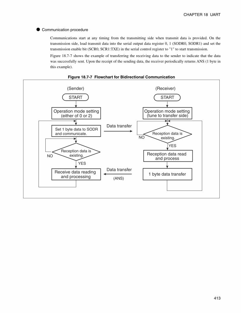
CHAPTER 18 UART
Communication procedure
Communications start at any timing from the transmitting side when transmit data is provided. On the
transmission side, load transmit data into the serial output data register 0, 1 (SODR0, SODR1) and set the
transmission enable bit (SCR0, SCR1:TXE) in the serial control register to "1" to start transmission.
Figure 18.7-7 shows the example of transferring the receiving data to the sender to indicate that the data
was successfully sent. Upon the receipt of the sending data, the receiver periodically returns ANS (1 byte in
this example).
Figure 18.7-7 Flowchart for Bidirectional Communication
(Sender) (Receiver)
START START
Data transfer
Data transfer
Operation mode setting Operation mode setting
1 byte data transferReceive data reading and processing
(either of 0 or 2)
Set 1 byte data to SODRand communicate.
Reception data is existing.
Reception data is existing.
(tune to transfer side)
Reception data read and process
NO
NO
YES
YES
(ANS)
413

CHAPTER 18 UART
18.7.4 Master/Slave Mode Communication Function (Multi-processor mode)
Operation mode 1 allows communication between multiple CPUs connected in a master/slave configuration. However, this is available only as master.
Master/Slave Mode Communication FunctionTo operate UART in the multi-processor mode (operation mode 1), the settings described in Figure 18.7-8
must be executed.
Figure 18.7-8 UART Operation Mode 1 Setting
Inter-CPU connection
One master CPU and two or more slave CPUs are connected to a pair of common communication lines to
make up the master/slave communication system as shown in Figure 18.7-9. The UART1 can be used only
as the master CPU.
Figure 18.7-9 Connection Example for UART Master-slave Communications
: Used bit: Unused bit: Set to "1": Set to "0": Set to "0" when using input of pin
SCR0, SCR1,SMR0, SMR1
SSR0, SSR1,SIDR0, SIDR1/SODR0, SODR1
Setting transfer data (at writing)/Holding receive data (at reading)
bit15 bit14 bit13 bit12 bit11 bit10 bit9 bit8 bit7 bit6 bit5 bit4 bit3 bit2 bit1 bit0
PEN P SBL CL AD REC RXE TXE MD1 MD0 SCKL M2L2 M2L1 M2L0 SCKE SOE
PE ORE FRE RDRF TDRE BDS RIE TIE
0 0
01
1 10
DDR4 D47 D46 D45 D44 D43 D42 D41 D40
Master CPU
SOT0,SOT1
SIN0,SIN1
SOT SIN SOT SIN
Slave CPU #0 Slave CPU #1
414

CHAPTER 18 UART
Function Selection
When it comes to master/slave communication, select the operation mode and data transfer direction, as
shown in Table 18.7-2. Since the parity check function cannot be used in operation mode 1, set the parity
enable bit (SCR0, SCR1:PEN) to "0".
Communication procedure
The communication starts when the master CPU transmits the address data. The address data, having an A/
D bit as 1, locates the slave CPU as the destination. Each slave CPU identifies the address data based on the
program, and if there is a match with the address that is already assigned, the slave CPU communicates
(typical data) with the master CPU.
Figure 18.7-10 shows the flowchart of the master/slave communication (multiprocessor mode).
Table 18.7-2 Select of Master/Slave Communication Function
Operating mode
Data ParitySynchronous
typeStop bit
Master CPU
Slave CPU
AddressTrans-mission/
Reception
Mode 1 -
AD= 1 +
8 bitsAddress
Not provided Asynchronous 1 bitor
2 bitsDataTrans-mission/
Reception
AD= 0 +
8 bitsData
415

CHAPTER 18 UART
Figure 18.7-10 Flowchart for Master/Slave Communications
(Master CPU)
START
Set SIN pin to Serial data input
Set AD to "0"
Receive operation enabled
Receive operation disabled
END
Slave CPU andcommunication
Communication end?
Other slave CPU and communication
Setting operating mode to "1"
Set 1 byte data (address data) selecting the slave CPU to D0 to D7and transfer(AD=1)
NO
NO
YES
YES
416

CHAPTER 18 UART
18.8 Notes on Using UART
Use of the UART requires the following cautions.
Notes on Using UART
Enabling sending and receiving
• The bits indicating that sending operation is enabled (SCR0, SCR1: TXE) and that receiving operation is
enabled (SCR0, SCR1: RXE) is provided for sending and receiving respectively.
• In the initial state after a reset, transmission and reception are both disabled (SCR0, SCR1:TXE=0,
RXE=0). Transmission and reception must therefore be enabled in advance.
• The device can stop transmission and reception by disabling them (SCR0, SCR1:TXE=0,RXE=0).
Setting operation mode
Set the operation mode after disabling transmission and reception (SCR0, SCR1:TXE=0,RXE=0). When
the operation mode is changed during transmission or reception, the transmitted/received data is not
guaranteed.
About clock synchronous mode
Operation mode 2 is set as a clock synchronizer method. Transmit/receive data is associated with no start
and stop bits.
Transmission interrupt enable timing
The sending data empty flag bit (SSR0, SSR1: TDRE) is set to "1" (no sending data, enabled to write
sending data) by default after resetting. So, as soon as a sending interrupt is enabled (SSR0, SSR1: TIE=1),
the sending interrupt request is generated. Be sure to prepare data to transmit before enabling transmission
(SSR0, SSR1:TIE=1).
Receiving Multiprocessor mode
In the multiprocessor mode, receiving operation based on 9-bit receipt is not allowed.
417

CHAPTER 18 UART
18.9 Example of UART Programming
This section provides program example for UART.
Example of UART Programming
Processing specification
Perform serial transmission/reception using the bidirectional communication function (normal mode) of the
UART.
Defined as: Operation mode 0, asynchronous, 8 bits of data length, 2 bits of stop bit length, without parity.
Use the P42/A10/SIN0, P43/A11/SOT0 pins for communication.
The baud rate is set to about 9600 bps using the dedicated baud rate generator.
Send character "13H" from the SOT0 pin to receive using an interrupt.
Set the machine clock (φ) to 16 MHz.
Coding example
ICR14 EQU 0000BEH ; UART send/receive interrupt control register.
DDR4 EQU 000014H ; Port 4 direction register 0
SMR0 EQU 000020H ; Serial mode register 0
SCR0 EQU 000021H ; Serial control register 0
SIDR0 EQU 000022H ; Serial input data register 0
SODR0 EQU 000022H ; Serial output data register 0
SSR0 EQU 000023H ; Serial Status Register 0
UTCR0 EQU 000025H ; UART prescaler control register 0
UTRLR0 EQU 000024H ; UART prescaler reload register 0
REC EQU SCR:2 ; Receive error flag clear bit
;----------Main Program------------------------------------------------------------
CODE CSEG ABS = 0FFH
START:
; : ; Initialize such as a stack pointer (SP).
; Defined as done.
AND CCR,#0BFH ; Disables the interrupt.
MOV I:ICR14, #00H ; Interrupt levels 0 (strength)
MOV I:DDR4, #00000000B ; Sets the SIN0 pin for input.
MOV I:SMR0, #00000001B ; operation mode 0 (asynchronous)
; Disables the clock output and enables the data
; output.
MOV I:UTRL0#81A0H ; uses Dedicated baud rate generator
; (9615bps Selection)
418

CHAPTER 18 UART
MOV I:SCR0, #00110011B ; Parity none and stop bit 2 bits
; Data length 8 bits and reception clear error flag
; Enables the transmission/reception operation
MOV I:SSR0, #00000010B ; sending interrupt disabled, receiving interrupt
; enabled
MOV I:SODR0, #13H ; Transmission data writing
MOV ILM, #07H ; Sets ILM in PS to level 7
OR CCR, #40H ; Interruption permission
LOOP: MOV A,#00H ; infinite loop
MOV A,#01H
BRA LOOP
;----------Interrupt Program------------------------------------------------------------
WARI:
MOV A, SIDR0 ; Reading receive data
CLRB I:REC ; The reception interrupt request flag is clear.
; :
; User processing
; :
RETI ; Returns from interrupt.
CODE ENDS
;----------Vector Settings------------------------------------------------------------------
VECT CSEG ABS=0FFH
ORG 0FF60H ; The vector is set in interruption #39(27H).
DSL WARI
ORG 0FFDCH ; Reset vector setting
DSL START
DB 00H ; Set to Single-chip mode
VECT ENDS
419

CHAPTER 18 UART
420

CHAPTER 19
I2C INTERFACE
This chapter gives an overview of I2C interface, the configuration and functions of registers, and operations
of I2C interface.
19.1 I2C Interface Outline
19.2 I2C Interface Register
19.3 I2C Interface Operation
421

CHAPTER 19 I2C Interface
19.1 I2C Interface Outline
I2C interface is Serial I/O by which Inter IC BUS is supported. Operates as the master/
slave devices on I2C bus.
I2C Interface Function
The I2C interface has the following functions:
• Master/slave sending and receiving
• Arbitration function
• Clock synchronous function
• Slave address/General call address detection function
• Forwarding direction detection function
• Repetitive generation and detection function of the start condition
• Bus error detection function
422

CHAPTER 19 I2C Interface
Block Diagram of I2C Interface
Figure 19.1-1 shows the block diagram of I2C interface.
Figure 19.1-1 Block Diagram of I2C Interface
SCL0
SDA0IRQ #17
Peripheral clock
Shift clock generation
Clock selection 1
Clock selection 2
Clock divider 1
Clock divider 2
Shift clockedge changetiming
Bus busy
Repeat start
Start
Master
Slave
ACK enable
GC-ACK enable
Error
F2 M
C-1
6LX
bus
Interrupt request
End
Start
Condition detection
Stop
Start
Condition generation
Stop
Slave addresscompareGlobal call
Arbitration lost detection
Send/receive
I2C enableICCR
ICCR
EN
CS4
CS3
CS2
CS1
CS0
IBSR
BB
RSC
LRB
TRX
FBT
AL
IBCR
BER
BEIE
INTE
INT
IBCR
SCC
MSS
ACK
GCAA
IBSR
AAS
GCA
IDAR
IADR
First Byte
Last Bit
2 4 8 16 32 64 128 256
5 6 7 8
Sync
423

CHAPTER 19 I2C Interface
19.2 I2C Interface Register
The configuration and functions of registers used in the I2C interface are described.
Register List of I2C Interface
Figure 19.2-1 Register List of I2C Interface
I2C Bus status registerch.0:000070H
IBSR0
00000000B
IBCR0ch.0:000071H
00000000B
I2C Bus status register
ICCR0
ch.0:000072HI2C Clock control register
--0XXXXXB
IADR0
ch.0:000073HI2C Bus address register
I2C Bus data register
-XXXXXXXB
IDAR0
ch.0:000074HXXXXXXXXB
Initial value
Initial value
Read/Write
Read/Write
Initial valueRead/Write
Initial valueRead/Write
Initial valueRead/Write
7 6 5 4 3 2 1 0
7 6 5 4 3 2 1 0
7 6 5 4 3 2 1 0
15 14 13 12 11 10 9 8
R/W R/W R/W R/W R/W R/W R/W R/W
R/W R/W R/W R/W R/W R/W R/W
R/W R/W R/W R/W R/W R/W
R/W R/W R/W R/W R/W R/W R/W R/W
R R R R R R R R
BB RSC AL LRB TRX AAS GCA FBT
BER BEIE SCC MSS ACK GCAA INTE INT
EN CS4 CS3 CS2 CS1 CS0
A6 A5 A4 A3 A2 A1 A0
D7 D6 D5 D4 D3 D2 D1 D0
15 14 13 12 11 10 9 8
424

CHAPTER 19 I2C Interface
19.2.1 I2C Bus Status Register 0 (IBSR0)
The configuration and functions of I2C bus status register 0 (IBSR0) are described.
I2C Bus Status Register 0 (IBSR0)
Figure 19.2-2 shows the bit configuration of I2C bus status registers 0 (IBSR0).
Figure 19.2-2 Bit Configuration of I2C Bus Status Register 0(IBSR0)
The function of each bit of the I2C bus status registers 0 (IBSR0) is described as follows.
[bit7] BB: Bus Busy
It is a bit shown the state of the I2C bus.
[bit6] RSC: Repeated Start Condition
It is a start condition detection repeatedly bit.
Is cleared either by writing "0" in INT bit, with no addressing on the slave connection, or by detecting the
start condition during the halted bus, or by detecting the stop condition.
[bit5] AL: Arbitration Lost
It is an arbitration lost detection bit.
It is cleared by writing "0" in INT bit.
ch.0:000070HI2C Bus status registerIBSR0
00000000BInitial value
7 6 5 4 3 2 1 0
R R R R R R R R
BB RSC AL LRB TRX AAS GCA FBT
0 Stop condition is detected.
1 Start condition is detected. (The bus is used.)
0 The start condition is not repeatedly detected.
1 The start condition was detected in the bus Occupied again.
0 The arbitration lost is not detected.
1 When arbitration lost has occurred on master transmission, or when other systems areusing the bus, "1" was written in MSS bit.
425

CHAPTER 19 I2C Interface
[bit4] LRB: Last Received bit
It is the acknowledgement storage bit. Stores the acknowledge from the receiver.
It is cleared by detecting the start condition or the stop condition.
[bit3] TRX: Transfer/Receive
It is the bit indicating sending and receiving of data transfer.
[bit2] AAS: Addressed As Slave
It is Addressing detection bit.
It is cleared by detecting of the start condition or stop condition.
[bit1] GCA: General Call Address
It is General call address (00H) detection bit.
It is cleared by detecting of the start condition or stop condition.
[bit0] FBT: First Byte Transfer
It is a first byte detection bit.
It is cleared either if "0" is written in INT bit or if no addressing is provided on the slave connection, even
though detection of the start condition has set "1".
0 Reception is acknowledged
1 Reception is not acknowledged
0 Receiving State
1 Transmission state
0 Addressing is not done at the slave.
1 Addressing was done at the slave.
0 The General call address is not received at the slave.
1 The General call address was received at the slave.
0 Received data is things except the first byte.
1 Received data is a first byte (address data).
426

CHAPTER 19 I2C Interface
19.2.2 I2C Bus Control Register 0 (IBCR0)
The configuration and functions of I2C bus control register 0 (IBCR0) are described.
I2C Bus Control Register 0 (IBCR0)Figure 19.2-3 shows the bit configuration of bus control register 0(IBCR0).
Figure 19.2-3 Bit Configuration of I2C Bus Control Register 0 (IBCR0)
The function of each bit of the bus control registers 0 (IBCR0) is described as follows:
[bit15] BER: Bus ERror
It is Bus error Interrupt request flag. Functions in writing phase differ from those as follows.
(at writing)
(at reading)
If BER bit is set, EN bit of ICCR register is cleared, the I2C interface goes into a halted state, and data
transfer is terminated.
[bit14] BEIE: Bus Error Interrupt Enable
It is bus error Interrupt enable bit.
The interruption is generated if the BER bit is "1" when this bit is "1".
ch.0:000071H
IBCR0
00000000B
I2C Bus status registerInitial valueRead/WriteR/W R/W R/W R/W R/W R/W R/W R/W
BER BEIE SCC MSS ACK GCAA INTE INT
15 14 13 12 11 10 9 8
0 Clear bus error interrupt request flag.
1 No effect on operation
0 The bus error is not detected.
1 Illegal start and stop condition was detected during data transfer.
0 Bus error interrupt disabled
1 Bus error interrupt enabled
427

CHAPTER 19 I2C Interface
[bit13] SCC: Start Condition Continue
It is a start condition generation bit.
(at writing)
This bit is always "0" at the beginning of reading.
[bit12] MSS: Master Slave Select
It is Master/slave selection bit.
If the arbitration lost has occurred during the master sending, it will be cleared and will switch to the slave
mode.
Note:
Because it is not possible to receive it as a slave on the following condition, the transmission of thegeneral call address is prohibited.
• When (1) other LSI with the master mode function without this LSI exists on the bus, (2) this LSItransmits the general call address as master, and (3) the arbitration lost is generated since thesecond byte.
[bit11] ACK: ACKnowledge
It is the acknowledge generation enable bit when the data is received.
Is invalid during receiving address data in the slave.
[bit10] GCAA: General Call Address Acknowledge
It is an acknowledge generating enable bit, when you receive the General call address.
[bit9] INTE: INTerrupt Enable
It is Interrupt enable bits.
The interruption is generated if the INT bit is "1" when this bit is "1".
0 No effect on operation
1 A start condition is regenerated on master transmission.
0 Generates the stop condition, and goes into the slave mode after the completion of transmission.
1 Goes into the master mode, generates the start condition, and starts transferring.
0 Acknowledgement is disabled to be generated.
1 Acknowledgement is enabled to be generated.
0 Acknowledgement is disabled to be generated
1 Acknowledgement is enabled to be generated.
0 Disables the interrupt.
1 Enables the interrupt.
428

CHAPTER 19 I2C Interface
[bit8] INT: INTerrupt
It is transfer stop interrupt request flag bit.
(at writing)
(at reading)
The SCL line is kept at "L" level at "1". Is cleared by writing "0", releases SCL line, and sends the
subsequent bite. And is reset to "0" by occurrence of the start condition or the stop condition on the master
connection.
Notes:
When an instruction which generates a start condition is executed (the MSS bit is set to "1") at the timingshown in Figure 19.2-4 and Figure 19.2-5, arbitration lost detection (AL bit=1) prevents an interrupt (INTbit=1) from being generated.
• Condition 1 in which an interrupt (INT bit=1) upon detection of "AL bit=1" does not occur.
When an instruction which generates a start condition is executed (setting the MSS bit in the IBCR registerto "1") with no start condition detected (BB bit=0) and with the SDA or SCL pin at the "L" level.
Figure 19.2-4 Diagram of Timing at which an Interrupt upon Detection of "AL bit=1" does not Occur
0 Clear Transfer stop interrupt request flag.
1 No effect on operation
0 Transfer has not been finished yet.
1
This is set when 1 byte of data including the ACK bit has already been transferred and ifthe following condition is applied.• It is a bus master.• It is a slave that the address is done.• The General call address was received.• The arbitration lost happened.• Other systems tried to generate a start condition while the bus was in use.
"L"
"L"
SCL pin
SCL or SDA pin at "L" level
SDA pin
I2C operation enable state (EN bit=1)
Master mode setting (MSS bit=1)
Arbitration lost detection (AL bit=1)
Bus busy (BB bit)
Interrupt (INT bit)
1
0
0
429

CHAPTER 19 I2C Interface
• Condition 2 in which an interrupt (INT bit=1) upon detection of "AL bit=1" does not occur
When an instruction which generates a start condition by enabling I2C operation (EN bit=1) is executed
(setting the MSS bit in the IBCR register to "1") with the I2C bus occupied by another master.
This is because, as shown in Figure 19.2-5, when the other master on the I2C bus starts communication
with I2C disabled (EN bit=0), the I2C bus enters the occupied state with no start condition detected (BBbit =0).
Figure 19.2-5 Diagram of Timing at which an Interrupt upon Detection of "AL bit=1" does not Occur
If a symptom as described above can occur, follow the procedure below for software processing.
1. Execute the instruction that generates a start condition (set the MMS bit to "1").
2. Use, for example, the timer function to wait for the time* for three-bit data transmission at the I2C transferfrequency set in the ICCR register.
Example: Time for three-bit data transmission at an I2C transfer frequency of 100 kHz 1/(100x103)x3=30 ms
3. Check the AL and BB bits in the IBSR register and, if the AL and BB bits are "1" and "0", respectively, set
the EN bit in the ICCR register to "0" to initialize I2C. When the AL and BB bits are not so, perform normalprocessing.
0
0
DATASLAVE ADDRESS
Stop ConditionStart Condition
The INT bit interrupt does not occur in the ninth clock cycle.
SCL pin
SDA pin
EN bit
MSS bit
AL bit
BB bit
INT bit
ACKACK
430

CHAPTER 19 I2C Interface
A sample flow is given below.
*: When "arbitration lost" is detected, the MSS bit is set to "1" and then the AL bit is set to "1" without failure
after the time for three-bit data transmission at the I2C transfer frequency.
• Example of occurrence of an interrupt (INT bit=1) upon detection of "AL bit=1"
When an instruction which generates a start condition is executed (setting the MSS bit to "1") with "busbusy" detected (BB bit=1) and arbitration is lost, the INT bit interrupt occurs upon detection of "ALbit=1".
Figure 19.2-6 Diagram of Timing at which an Interrupt upon Detection of "AL bit=1" Occurs
BB bit=0 and AL bit=1?NO
YES
Set the EN bit to 0 to initialize I2Cto normal process
Master mode settingSet the MSS bit in the bus control register (IBCR) to 1.
Wait* for the time for three-bit data transmission at the I2Ctransfer frequency set in the clock control register (ICCR).
DATASLAVE ADDRESS
Start Condition Interrupt in the ninth clock cycle
SCL pin
EN pin
MSS pin
Clearing the AL bit by software
Releasing the SCL by clearing the INT bit by software
AL pin
BB pin
INT pin
SDA pin ACK
431

CHAPTER 19 I2C Interface
Notes on Use of I2C Bus Control Register 0 (IBCR0)The following care should be taken to conflicts among SCC bit, MSS bit, and INT bit.
Writing to SCC bit, MSS bit, INT bit simultaneously causes conflicts of transferring the next bite, occurrence
of the start condition, and occurrence of the stop condition. The priority in this case is as follows.
The following byte forwarding and stop condition generation
If "0" is written in INT bit and "0" in MSS bit, writing "0" in MSS bit is preferred and the stop condition
occurs.
The following byte forwarding and start condition generation
If "0" is written in INT bit and "1" in SCC bit, writing "1" in SCC bit is preferred and the start condition
occurs.
Start condition generation and stop condition generation
Simultaneous writing is disabled that not only "1" is written in SCC bit but also "0" is written in MSS bit.
432

CHAPTER 19 I2C Interface
19.2.3 I2C Bus Clock Control Register 0 (ICCR0)
The configuration and functions of I2C bus clock control register 0 (ICCR0) are described.
I2C Bus Clock Control Register 0 (ICCR0)
Figure 19.2-7 shows the bit configuration of I2C bus clock control registers 0 (ICCR0).
Figure 19.2-7 Bit Configuration of I2C Bus Clock Control Register 0 (ICCR0)
The functions of I2C bus clock control registers 0 (ICCR0) are described below.
[bit7, bit6] Undefinition bit
The read value is irregular. Nothing is affected when it is written.
[bit5] EN: ENable
It is an operation permission bit in the I2C interface.
• When "0", each bit of IBSR register and IBCR register (except BER and BEIE bits) is cleared.
• Is cleared when BER bit is set.
[bit4 to bit0] CS4 to CS0:Clock Period Select 4-0
It is the bit which sets the serial clock frequency. The frequency fsck in the shift clock is set as shown in
the next formula.
Note:
The cycle + 4 is minimum overhead for checking that the output level of SCL pin has changed. Ifdelay is longer on the rising edge of SCL pin, or a slave device delays a clock, it exceeds this value.Note that the frequency of the serial clock must be set to 100 kHz or less.
m and n for CS4 to CS0 is as shown in Table 19.2-1.
ch.0:000072H ICCR0
I2C bus clock control registerXX0XXXXXBInitial value
7 6 5 4 3 2 1 0
R/W R/W R/W R/W R/W R/W
EN CS4 CS3 CS2 CS1 CS0
0 Operation disabled
1 Operation enabled
4nmfsck : Machine clock
φ φ
433

CHAPTER 19 I2C Interface
Table 19.2-1 Setting of Serial Clock Frequency
m CS4 CS3 n CS2 CS1 CS0
5 0 0 4 0 0 0
6 0 1 8 0 0 1
7 1 0 16 0 1 0
8 1 1 32 0 1 1
64 1 0 0
128 1 0 1
256 1 1 0
512 1 1 1
434

CHAPTER 19 I2C Interface
19.2.4 I2C Bus Address Register 0 (IADR0)
The configuration and functions of I2C bus address register 0 (IADR0) are described.
I2C Bus Address Register 0 (IADR0)
Figure 19.2-8 shows the bit configuration of the I2C bus address registers 0 (IADR0).
Figure 19.2-8 I2C Bus Address Register 0 (IADR0)
[bit14 to bit8] A6 to A0
It is a slave address bit. It is a register which specifies the slave address. In the slave, the address data is
compared to the IDAR register upon reception of the address, and if they match, then it will send the
acknowledge to the master.
ch.0:000073HIADR0I2C bus address register
XXXXXXXXBInitial value
15 14 13 12 11 10 9 8
R/W R/W R/W R/W R/W R/W R/W
A6 A5 A4 A3 A2 A1 A0
435

CHAPTER 19 I2C Interface
19.2.5 I2C Bus Data Register 0 (IDAR0)
The configuration and functions of I2C bus data register 0 (IDAR0) are described.
I2C Bus Data Register 0 (IDAR0)
Figure 19.2-9 shows the bit configuration of the I2C bus data registers 0 (IDAR0).
Figure 19.2-9 Bit Configuration of I2C Bus Data Register 0 (IDAR0)
[bit7 to bit0] D7 to D0
It is a data bit.
It is the data register used for the serial transfer, and transferred from MSB. During the data receiving
(TRX= 0), the data output value becomes "1".
The writing side of IDAR register is double buffering. If the bus is in use (BB=1), the data to be written
to is loaded to the register for serial transferring when each byte is transferred. In reading the register
for serial transferring is directly read, so the receiving data is valid only when INT bit is set.
ch.0:000074H
I2C Bus data registerIDAR0
XXXXXXXXBInitial value
7 6 5 4 3 2 1 0
R/W R/W R/W R/W R/W R/W R/W R/W
D7 D6 D5 D4 D3 D2 D1 D0
436

CHAPTER 19 I2C Interface
19.3 I2C Interface Operation
For I2C bus, 1 serial data line (SDA), 1 serial clock line (SCL), and 2 bidirectional bus
lines are responsible for communication. I2C interface, which has 2 open drain input-output pins (SDA and SCL) to them, allows wired logic.
Start Condition
If "1" is written to MSS bit in the state of the bus being released (BB=0 and MSS=0), I2C interface
generates the start condition as soon as it changes to the master mode. In the master mode the start
condition can be regenerated by writing "1" to SCC bit even though the bus is in use (BB=1). To generate
start conditions, 2 methods are provided as follows.
• Writing "1" to MSS bit in the state that the bus is not in use (MSS=0 * BB=0 * INT=0 * AL=0).
• Writing "1" to SEC bit in the state of interrupting in bus master (MSS=1 * BB=1 * INT=1 * AL=0).
When the bus (in the idle state) is used by other systems and if "1" is written to MSS bit, then AL bit is set
to "1". Writing to MSS bit and SCC bit in any other state than being mentioned above is ignored.
Stop ConditionWhen "0" is written to MSS bit in the state of the master mode (MSS=1), the stop condition is generated,
resulting in the slave mode. The condition to generate the stop condition is as follows.
Writing "0" to MSS bit in the state of interrupting in bus master (MSS=1 * BB=1 * INT=1 * AL=0).
Writing "0" excluding this in the MSS bit is disregarded.
AddressingIn the master mode, BB= 1 and TRX= 1 will be set after the start condition generation, and it outputs the
IDAR register contents from the MSB. After sending the address data, receives the acknowledgement from
the slave, reverses bit0 (bit0 of IDAR register that is already sent) of the sending data, and then stores it
into TRX bit.
In the slave mode, BB is set to "1" and TRX is set to "0" after the start condition is generated, and the
sending data from the master is received in IDAR register. After the address data is received, IDAR register
is compared with IADR register. If they matches, AAS is set to "1" and the acknowledgement is sent to the
master. Then, bit0 of the receiving data (bit0 of IDAR register that is already received) is stored in TRX bit.
ArbitrationIf other master are sending the data simultaneously in the master sending mode, the arbitration will occur.
When the sending data of its own is "1", and the data on SDA line is "L" level, it is considered that its
arbitration is lost and AL is set to "1". When an attempt is made that the start condition is generated in the
state the bus is in use as mentioned above, Al is also set to "1".When AL is set to "1", MSS is "0" and TRX
is "0", resulting in the slave receiving mode.
437

CHAPTER 19 I2C Interface
AcknowledgeThe receiver send the acknowledge to the sender. During data reception, ACK bit can specify acknowledgement
is necessary or not. During the data sending, the acknowledge from the receiver is stored in the LRB bit.
If the sender as slave does not receive any acknowledgement from the receiver as master, TRX becomes
"0", resulting in the slave receiving mode. This allows the master to generate the stop condition when the
slave releases the SCL line.
Bus Error
If the following conditions exist, it will be considered as bus error, and the I2C interface will be in the
stopped state.
• Detecting of violation of the basic rules on I2C bus during data transfer (including Ack bit)
• Stop condition detection at master
• Detecting of violation of the basic rules on I2C bus in bus idle
The Others
Processing after arbitration lost is detected
After arbitration lost occurs, must decide if it is addressed or not by software.
Once arbitration lost occurs, it becomes slave from the viewpoint of hardware. After one byte of data
transfer both CLK line and DATA line are pulled to "L". For this reason, if addressing is done, CLK line
and DATA line should be released after slave transmission or slave reception is ready. if no addressing is
done, then CLK line and DATA line should be immediately released. (Software is responsible for this all.)
Interruption factor when arbitration lost is detected
When arbitration lost is detected, causes of interrupts are not issued immediately but after one byte of data
has been transferred.
When arbitration lost is detected, it becomes slave from the viewpoint of hardware. Even if so, it outputs 9
clocks in all in order to issue causes of interrupts. For this reason, causes and interrupts are not immediately
issued, so no processing is allowed after arbitration lost.
Interrupt condition
It is specified that I2C bus has one interrupt and causes of interrupts are issued once one byte of transfercompletes or if the conditions of interrupts are satisfied.
Each flag should be checked within the interrupt routine, since multiple conditions of interrupts isidentified based on one interrupt. Multiple conditions of interrupts on completion of one byte transfer is asfollows.
• When it is a bus master
• When it is a slave that the address is done
• When you receive the General call address
• When arbitration lost has occurred.
Transfer rate
Note that I2C bus can support up to 100 kHz of the serial clock frequency of transmission.
438

CHAPTER 19 I2C Interface
19.3.1 Transfer Flow of I2C Interface
Figure 19.3-1 shows the 1-byte transfer flow from master to slave, and Figure 19.3-2 shows the 1-byte transfer flow from slave to master.
Transfer Flow of I2C Interface
Figure 19.3-1 1-byte Transfer Flow from the Master to Slave
Master SlaveStart
IDAR: WritingMSS: Writing "1"
Start conditionBB set, TRX set BB set, TRX set
Address data transferAAS set
AcknowledgementLRB reset
INT set,TRX set INT set,TRX setIDAR: Writing Interrupt
Interrupt
ACK: Writing "1"INT : Writing "0" INT: Writing "0"
Data transfer
AcknowledgementLRB reset
INT set INT setIDAR: ReadINT: Writing "0"
MSS: Writing "0"INT resetBB reset,TRX reset Stop condition BB reset,TRX reset
AAS reset
End
439

CHAPTER 19 I2C Interface
Figure 19.3-2 1-byte Transfer Flow from Slave to Master
IDAR: WritingMSS: Writing "1"
BB set,TRX set BB set,TRX set
AAS reset
LRB reset
INT set,TRX reset INT set,TRX setIDAR: Writing
INT: Writing "0" INT: Writing "0"
LRB set,TRX set
INT set INT setIDAR: Read
INT: Writing "0"MSS: Writing "0"INT resetBB reset,TRX reset BB reset,TRX reset
AAS reset
Master SlaveStart
Start condition
Address data transfer
Acknowledgement
Interrupt
Interrupt
Data transfer
Negative acknowledgement
Stop condition
End
440

CHAPTER 19 I2C Interface
19.3.2 Mode Flow of I2C Interface
Figure 19.3-3 shows the flow of mode transitions for the I2C interface.
Flow of I2C Interface Mode Transitions
Figure 19.3-3 I2C Mode Flow
Slave receive mode
SCCNO
YES
TRX,AAS,LRB:resetFBT:set
YESSCC&BB=1 RSC:set
NO
BB:set
8 bits received
Address comparison RSC,FBT:reset
Match
AAS: set Acknowledgement output
INT:set SCL line retained at "L"
NOTRX=1 Slave receive mode
YES YESSCC AAS,LRB,BB,RSC
Slave send mode :resetNO
INT: 0 write
FBT:resetSCL line freed
Send/receive
YESAcknowledgement
received?NO
TRX:reset
441

CHAPTER 19 I2C Interface
19.3.3 Operation Flow of I2C Interface
Figure 19.3-4 shows the operation flow of a master send/receive program (with
interrupts) for the I2C interface. Figure 19.3-5 shows the operation flow of the slave
program (with interrupts) for the I2C interface.
Operation Flow of I2C Interface
Figure 19.3-4 Operation Flow of the Master Send/Receive Program (with Interrupts) for the I2C Interface
Main routine
Start
Set the slave address
I2C operating enabled
Master receive operation?
NOMaster sendSet the number of bytes to be sent
for each time that data is written
Send the slave address set(Data direction bit=0)
BBbit=1?
NO
YES
Generate the start conditionwhile sending the slave address
Wait for a certainamount of time
NO
YESBB bit=0 andAL bit=1?
LOOP
Master receiveSet the number of bytes
to be sent for each time that data is written
BBbit=1?
NO
YES
NO
YES
LOOP
I2C operation disabled
Interrupt routine
Start
Bus erroroccurred?
NO
YES
AL occurred?
NO
Master?
YES
NO
Was ACKreturned?
YES
NO
Is the data direction bit (TRX)=1?
YES
NO
Is the number of remaining bytes to
be sent 0?
YES
NODecrement the number of bytes to be sent
Set the send data
Clear the end interrupt factor
RETI
Is the number of remaining bytes to
be received 0?
YES
NO
Is the number of remaining bytes to
be received 1?
YES
NO
Acknowledge occurrence enabled
Is the first bytebeing received?
YES
NODecrement the number of bytes to be received
Store the receive data to the RAM
Clear the end interrupt factor
RETI
STOP condition generated
RETI
Clear the bus error interrupt factor
I2C operation enabled
I2C initial setting
RETI
BB bit=0 andAL bit=1?
I2C operation disabled
Acknowledge occurrence enabled
Receive the slave address set(Data direction bit=1)
Generate the start conditionwhile sending the slave address
Acknowledge occurrence enabled
To the slave programinterrupt routine
1
3
1
2
2
3
3
1
1Wait for a certainamount of time
442

CHAPTER 19 I2C Interface
Figure 19.3-5 Operation Flow of the Slave Program (with Interrupts) for the I2C Interface
NO
YES
YES
NO
NO
YES
NO
RETI
RETI
Set slave mode
LOOP
Clear the transfer endinterrupt source
RETI
Set the send data
Is the receive data an
address?
NO
YES
RETI
YES
Main routine
Start
Set the slave address
I2C operation enabled
Interrupt routine
Start
Bus erroroccurred?
Is addressingcompleted?
Is ACKreturned?
Is the data direction bit (TRX)=1?
Clear the transfer end interrupt source
Store the datain RAM
Clear the transfer endinterrupt source
Clear the bus error interrupt factor
I2C operation enabled
I2C initial setting
1
1
1
2
2
443

CHAPTER 19 I2C Interface
444

CHAPTER 20ROM MIRROR FUNCTION
SELECTION MODULE
This chapter describes the ROM mirror function selection module.
20.1 Overview of ROM Mirror Function Select Module
20.2 ROM Mirror Function Select Register (ROMM)
445

CHAPTER 20 ROM MIRROR FUNCTION SELECTION MODULE
20.1 Overview of ROM Mirror Function Select Module
The ROM mirror function selection module is used to select via register settings an FF bank in ROM, whose contents can be viewed via bank 00.
Block Diagram of ROM Mirror Function Select ModuleFigure 20.1-1 shows the block diagram of ROM mirror function selection module.
Figure 20.1-1 Block Diagram of ROM Mirror Function Select Module
Register of ROM Mirror Function Selection ModuleFigure 20.1-2 shows the configuration of ROM mirror function select module.
Figure 20.1-2 ROM Mirror Function Selection Module Configuration
ROM mirror function selection
Address area
FF bank 00 bank
F2MC-16LX Bus
ROM
R/W
ROMM Address : 00006FH
bit initial valueReserved
W
MI
15 14 13 12 11 10 9 8
11B
446

CHAPTER 20 ROM MIRROR FUNCTION SELECTION MODULE
20.2 ROM Mirror Function Select Register (ROMM)
The configuration and functions of ROM Mirror Function Select Register (ROMM) are described.
ROM Mirror Function Select Register (ROMM)Figure 20.2-1 shows the bit configuration of ROM mirror function select register (ROMM).
Figure 20.2-1 Bit Configuration of ROM Mirror Function Select Register (ROMM)
[bit9] Reserved bit
It is Reserved bit. Please write "1".
[bit8] MI
• When "1" is written, ROM data in FF bank can be also read in 00 bank.
• When "0" is written, this function is not available to 00 bank.
• Only writing is enabled.
Notes:
• Do not access to ROMM register in the middle of the operation of the address 008000H to00FFFFH.
• When ROM mirror function is activated, the addresses from FF8000H to FFFFFFH are mirrored tothe addresses from 008000H to 00FFFFH of 00 bank. So ROM addresses under the addressFF7FFFH are not mirrored even though ROM mirror function is set.
R/W
ROMM Address : 00006FH
bit initial valueReserved
W
MI
15 14 13 12 11 10 9 8
11B
447

CHAPTER 20 ROM MIRROR FUNCTION SELECTION MODULE
448

CHAPTER 21ADDRESS MATCH
DETECTION FUNCTION
This chapter explains the address match detection function and its operation.
21.1 Overview of Address Match Detection Function
21.2 Block Diagram of Address Match Detection Function
21.3 Configuration of Address Match Detection Function
21.4 Explanation of Operation of Address Match Detection Function
21.5 Program Example of Address Match Detection Function
449

CHAPTER 21 ADDRESS MATCH DETECTION FUNCTION
21.1 Overview of Address Match Detection Function
If the address of the instruction to be processed next to the instruction currently processed by the program matches the address set in the detect address setting registers, the address match detection function forcibly replaces the next instruction to be processed by the program with the INT9 instruction to branch to the interrupt processing program. Since the address match detection function can use the INT9 interrupt for instruction processing, the program can be corrected by patch processing.
Overview of Address Match Detection Function• The address of the instruction to be processed next to the instruction currently processed by the program
is always held in the address latch through the internal bus. The address match detection function always
compares the value of the address held in the address latch with that of the address set in the detect
address setting registers. When these compared values match, the next instruction to be processed by the
CPU is forcibly replaced by the INT9 instruction, and the interrupt processing program is executed.
• There are two detect address setting registers (PADR0 and PADR1), each of which has an interrupt
enable bit. The generation of an interrupt due to a match between the address held in the address latch
and the address set in the detect address setting registers can be enabled and disabled for each register.
450

CHAPTER 21 ADDRESS MATCH DETECTION FUNCTION
21.2 Block Diagram of Address Match Detection Function
The address match detection module consists of the following blocks:• Address latch• Address detection control register (PACSR)• Detect address setting registers (PADR0/PADR1)
Block Diagram of Address Match Detection FunctionFigure 21.2-1 shows the block diagram of the address match detection function.
Figure 21.2-1 Block Diagram of the Address Match Detection Function
Address latch
The address latch stores the value of the address output to the internal data bus.
Address detection control register (PACSR)
The address detection control register enables or disables output of an interrupt at an address match.
Detect address setting registers (PADR0, PADR1)
The detect address setting registers set the address that is compared with the value of the address latch.
Note:
The addresses of the detect address setting register are 1FF0H to 1FF5H and are included in theRAM area. Therefore, the access to the RAM area should not be performed during the use of thisfunction (only MB90V330A).
PADR0 (24bit)
Reserved Reserved Reserved AD1E Reserved AD0E
PACSR
Detect address setting register 0
Address detection control register (PACSR)
Detect address setting register 1
Address latch
PADR1 (24bit)
INT9 instruction (INT9 interrupt
generation)
Reserved Reserved
Inte
rnal
dat
a bu
s
Reserved: Always set to "0"
Com
para
tor
451

CHAPTER 21 ADDRESS MATCH DETECTION FUNCTION
21.3 Configuration of Address Match Detection Function
This section details the registers used by the address match detection function.
List of Registers and Reset Values of Address Match Detection Function
Figure 21.3-1 List of Registers and Reset Values of Address Match Detection Function
Detect address setting register 1 (PADR1): Middle
15 14bit 13 12 11 10 9 8
Detect address setting register 1 (PADR1): Low
7 6bit 5 4 3 2 1 0
7 6 5 4 3 2 1 0
7 6 5 4 3 2 1 0
Detect address setting register 0 (PADR0): Low
bit
15 14 13 12 11 10 9 8
Detect address setting register 1 (PADR1): High
bit
Detect address setting register 0 (PADR0): High
bit
Detect address setting register 0 (PADR0): Middle
bit
Address detection control register (PACSR)
7 6 5 4 3 2 1 0
× ×××× ×××
× ×××× ×××
× ×××× ×××
× ×××× ×××
× ×××× ×××
× ×××× ×××
bit
7 6 5 4 3 2 1 0
0 0000 000
× : Undefined
Address : 009EH
Address : 1FF2H
Address : 1FF1H
Address : 1FF0H
Address : 1FF5H
Address : 1FF4H
Address : 1FF3H
452

CHAPTER 21 ADDRESS MATCH DETECTION FUNCTION
21.3.1 Address Detection Control Register (PACSR)
The address detection control register (PACSR) enables or disables output of an interrupt at an address match. When an address match is detected when output of an interrupt at an address match is enabled, the INT9 interrupt is generated.
Address Detection Control Register (PACSR)
Figure 21.3-2 Address Detection Control Register (PACSR)
Reset value
00000000B
45 3 2 1 07 6
R/WR/WR/WR/WR/WR/W R/WR/W
AD0E
0
1
Address match detection enable bit 0
Disables address match detection in PADR0
Enables address match detection in PADR0
bit 1
AD1E
0
1
Address match detection enable bit 1
Disables address match detection in PADR1
Enables address match detection in PADR1
bit 3
Reserved
0
Reserved bit
Always set to "0"
bit 4
Reserved
0
Reserved bit
Always set to "0"
bit 0
Reserved
0
Reserved bit
Always set to "0"
bit 2
Reserved
0
Reserved bit
Always set to "0"
bit 5
Reserved
0
Reserved bit
Always set to "0"
bit 6
Reserved
0
Reserved Reserved Reserved Reserved Reserved Reserved
Reserved bit
Always set to "0"
bit 7
R/W : Read/Write : Reset value
Address
009EHAD0EAD1E
453

4
CHAPTER 21 ADDRESS MATCH DETECTION FUNCTION
54
Table 21.3-1 Functions of Address Detection Control Register (PACSR)
Bit Name Function
bit7 to bit4
Reserved: reserved bit Always set to "0".
bit3AD1E: Address match detection enable bit1
The address match detection operation with the detect address setting register 1 (PADR1) is enabled or disabled.When set to "0": Disables the address match detection operation.When set to "1": Enables the address match detection operation.• When the value of detect address setting registers 1 (PADR1) matches
with the value of address latch at enabling the address match detection operation (ADE0 = 1), the INT9 instruction is immediately executed.
bit2 Reserved: reserved bit Always set to "0".
bit1AD0E:Address match detection enable bit0
The address match detection operation with the detect address setting register 0 (PADR0) is enabled or disabled.When set to "0": Disables the address match detection operation. When set to "1": Enables the address match detection operation.• When the value of detect address setting register 0 (PADR0) matches
with the value of address latch at enabling the address match detect operation (ADE0 = 1), the INT9 instruction is immediately executed.
bit0 Reserved: reserved bit Always set to "0".

CHAPTER 21 ADDRESS MATCH DETECTION FUNCTION
21.3.2 Detect Address Setting Registers (PADR0, PADR1)
The value of an address to be detected is set in the detect address setting registers. When the address of the instruction processed by the program matches the address set in the detect address setting registers, the next instruction is forcibly replaced by the INT9 instruction, and the interrupt processing program is executed.
Detect Address Setting Registers (PADR0, PADR1)
Figure 21.3-3 Detect Address Setting Registers (PADR0H, PADR0M, PADR0L, PADR1H, PADR1M, PADR1L)
R/W R/WR/WR/WR/W R/WR/WR/W
D11 D8D9D10D15 D12D13D14
bit 15 bit 14 bit 13 bit 12 bit 11 bit 10 bit 9 bit 8 Reset value
XXXXXXXXB
R/W R/WR/WR/WR/W R/WR/WR/W
D19 D16D17D18D23 D20D21D22
bit 7 bit 6 bit 5 bit 4 bit 3 bit 2 bit 1 bit 0 Reset value
XXXXXXXXB
R/W R/WR/WR/WR/W R/WR/WR/W
D3 D0D1D2D7 D4D5D6
bit 7 bit 6 bi t 5 bi t 4 bi t 3 bi t 2 bit 1 bit 0
PADR0, PADR1: High
PADR0, PADR1: Middle
Reset value
XXXXXXXXB
R/W : Read/WriteX : Undefined
PADR0, PADR1: Low
Address 1FF2H, 1FF5H
Address 1FF1H, 1FF4H
Address 1FF0H, 1FF3H
455

CHAPTER 21 ADDRESS MATCH DETECTION FUNCTION
Functions of Detect Address Setting Registers
• There are two detect address setting registers (PADR0, PADR1) that consist of a high byte (bank),
middle byte, and low byte, totaling 24 bits.
• In the detect address setting registers (PADR0, PADR1), starting address (first byte) of instruction to be
replaced by INT9 instruction should be set.
Figure 21.3-4 Setting of Starting Address of Instruction Code to be Replaced by INT9
Notes:
• When an address of other than the first byte is set to the detect address setting register (PADR0,PADR1), the instruction code is not replaced by INT9 instruction and a program of an interruptprocessing is not be performed. When the address is set to the second byte or subsequent, theaddress set by the instruction code is replaced by "01" (INT9 instruction code) and, which maycause malfunction.
• The detect address setting registers (PADR0, PADR1) should be set after disabling the addressmatch detection (PACSR: AD0E = 0 or AD1E = 0) of corresponding address match controlregisters. If the detect address setting registers are changed without disabling the address matchdetection, the address match detection function will work immediately after an address matchoccurs during writing address, which may cause malfunction.
• The address match detection function can be used only for addresses of the internal ROM area. Ifaddresses of the external memory area are set, the address match detection function will not workand the INT9 instruction will not be executed.
Table 21.3-2 Address Setting of Detect Address Setting Registers
Register Name Interrupt Output Enable Address Setting
Detect address setting register 0 (PADR0)
PACSR: AD0E
High Set the upper 8 bits of detect address 0 (bank).
Middle Set the middle 8 bits of detect address 0.
Low Set the lower 8 bits of detect address 0.
Detect address setting register 1 (PADR1)
PACSR: AD1E
High Set the upper 8 bits of detect address 1 (bank).
Middle Set the middle 8 bits of detect address 1.
Low Set the lower 8 bits of detect address 1.
Address
FF001C :FF001F :FF0022 :
Instruction code Mnemonic
Set to detect address (High : FFH, Middle : 00H, Low : 1FH)
MOVWMOVWMOVW
RW0, #0000A, #0000A,#0880
A8 00 004A 00 004A 80 08
456

CHAPTER 21 ADDRESS MATCH DETECTION FUNCTION
21.4 Explanation of Operation of Address Match Detection Function
If the addresses of the instructions executed in the program match those set in the detection address setting registers (PADR0, PADR1), the address match detection function will replace the first instruction with the INT9 instruction (01H) to branch to the
interrupt processing program.
Operation of Address Match Detection FunctionFigure 21.4-1 shows the operation of the address match detection function when the detect addresses are set
and an address match is detected.
Figure 21.4-1 Operation of Address Match Detection Function
Setting Detect Address1. Disable the detection address setting register 0 (PADR0) where the detect address is set for address
match detection (PACSR: AD0E = 0).
2. Set the detect address in the detection address setting register 0 (PADR0). Set "FFH" at the higher bits of
the detection address setting register 0 (PADR0), "00H" at the middle bits, and "1FH" at the lower bits.
3. Enable the detect address setting register 0 (PADR0) where the detect address is set for address match
detection (PACSR: AD0E = 1).
Program Execution1. If the address of the instruction to be executed in the program matches the set detect address, the first
instruction code at the matched address is replaced by the INT9 instruction code (01H).
2. INT9 instruction is executed. INT9 interrupt is generated and then interrupt processing program is
executed.
Address
FF001C :FF001F :FF0022 :
Replaced by INT9 instruction (01H)
Instruction code
A8 00 004A 00 004A 80 08
Mnemonic
MOVWMOVWMOVW
RW0, #0000A, #0000A, #0880
The instruction address to be executed by program matches detect address setting register 0
Program execution
457

CHAPTER 21 ADDRESS MATCH DETECTION FUNCTION
21.4.1 Example of Using Address Match Detection Function
This section gives an example of patch processing for program correction using the address match detection function.
System Configuration and E2PROM Memory Map
System configuration
Figure 21.4-2 gives an example of the system configuration using the address match detection function.
Figure 21.4-2 Example of System Configuration Using Address Match Detection Function
E2PROMMCU
MB90335
Storing patch program
SIN0
Serial E2PROMInterface
series
458

CHAPTER 21 ADDRESS MATCH DETECTION FUNCTION
E2PROM Memory Map
Figure 21.4-3 shows the allocation of the patch program and data at storing the patch program in E2PROM.
Figure 21.4-3 Allocation of E2PROM Patch Program and Data
Patch program byte count
The total byte count of the patch program (main body) is stored. If the byte count is "00H", it indicates that
no patch program is provided.
Detect address (24 bits)
The address where the instruction code is replaced by the INT9 instruction code due to program error is
stored. This address is set in the detection address setting registers (PADR0, PADR1).
Patch program (main body)
The program executed by the INT9 interrupt processing when the program address matches the detect
address is stored. Patch program 0 is allocated from any predetermined address. Patch program 1 is
allocated from the address indicating <starting address of patch program 0 + total byte count of patch
program 0>.
0 0 0 0 H
0 0 0 1 H
0 0 0 2 H
0 0 0 3 H
0 0 0 4 H
0 0 0 5 H
0 0 0 6 H
0 0 0 7 H
0 0 1 0 H
0 0 2 0 H
For patch program 0PADR0
AddressE2PROM
Patch program 1(main body)
Patch program 0(main body)
Patch program byte count
Detect address 0 (Low)
Detect address 0 (Middle)
Detect address 0 (High)
Patch program byte count
Detect address 1 (Low)
Detect address 1 (Middle)
Detect address 1 (High)
PADR1For patch program 1
459
CHAPTER 21 ADDRESS MATCH DETECTION FUNCTION
Setting and Operating State
Initialization
• E2PROM data are all cleared to "00H".
Occurrence of program error
• By using the connector (UART), information about the patch program is transmitted to the MCU
(MB90335 series) from the outside according to the allocation of the E2PROM patch program and data.
• The MCU (MB90335 series) stores the information received from outside in the E2PROM.
Reset sequence
• After reset, the MCU (MB90335 series) reads the byte count of the E2PROM patch program to check
the presence or absence of the correction program.
• If the byte count of the patch program is not "00H", the higher, middle and lower bits at detect addresses
0 and 1 are read and set in the detection address setting registers 0 and 1 (PADR0, PADR1). The patch
program (main body) is read according to the byte count of the patch program and written to RAM in
the MCU (MB90335 series).
• The patch program (main body) is allocated to the address where the patch program is executed in the
INT9 interrupt processing by the address match detection function.
• Address match detection is enabled (PACSR: ADE0 = 1, ADE1 = 1)
INT9 Interrupt processing
• Interrupt processing is performed by the INT9 instruction. The MB90335 series has no interrupt request
flag by address match detection. Therefore, if the stack information in the program counter is discarded,
the detect address cannot be checked. When checking the detect address, check the value of program
counter stacked in the interrupt processing routine.
• The patch program is executed, branching to the normal program.
460

461
CHAPTER 21 ADDRESS MATCH DETECTION FUNCTION
Operation of Address Match Detection Function at Storing Patch Program in E2PROM
Figure 21.4-4 shows the operation of the address match detection function at storing the patch
program in E2PROM.
Figure 21.4-4 Operation of Address Match Detection Function at Storing Patch Program in E2PROM
000000H
FFFFFFH
Program error
Detection address setting register
Patch program
Detection address setting(reset sequence) Serial E2PROM
interface
. Patch program byte count
. Address for address detection
. Patch program
E2PROM
(4)
(2)
(1)
(3)
ROM
RAM
(1) Execution of detection address setting of reset sequence and normal program(2) Branch to patch program which expanded in RAM with INT9 interrupt processing by address match detection(3) Patch program execution by branching of INT9 processing(4) Execution of normal program which branches from patch program

CHAPTER 21 ADDRESS MATCH DETECTION FUNCTION
Flow of Patch Processing
Figure 21.4-5 shows the flow of patch processing using the address match detection function.
Figure 21.4-5 Flow of Patch Processing
Reset
Read the 00H of E2PROM
Execution of patch program000400H to 000480H
Branch to patch programJMP 000400H
End of patch programJMP FF8050H
Enable address match detection(PACSR : AD0E = 1)
E2PROM : 0000H
= 0
Program addressPC= PADR0
Read detect address E2PROM : 0001H to 0003H
↓MCU : Set to PADR0
Read patch programE2PROM : 0010H to 008FH
↓MCU : 000400H to 00047FH
Execution of normal program
INT9
INT9
NO
YES
NO
YES
ROM
MB90335 series
Program error
Detection address setting register
Stack area
RAM area
Patch program
I/O area
Register/RAM area
RAM
FFFFFFH
FF8050H
FF8000H
FF0000H
000900H
000480H
000400H
000100H
000000H
E2PROM
Patch program
Detect address (High) : FFH
Detect address (Middle) : 80H
Detect address (Low) : 00H
Patch program byte count : 80H
0090H
0010H
0003H
0002H
0001H
0000H
FFFFH
462

CHAPTER 21 ADDRESS MATCH DETECTION FUNCTION
21.5 Program Example of Address Match Detection Function
This section gives a program example for the address match detection function.
Program Example for Address Match Detection Function
Processing specifications
If the address of the instruction to be executed by the program matches the address set in the detection
address setting register (PADR0), the INT9 instruction is executed.
Coding example
PACSR EQU 00009EH ; Address detection control register
PADRL EQU 001FF0H ; Detection address setting register 0 (Low)
PADRM EQU 001FF1H ; Detection address setting register 0 (Middle)
PADRH EQU 001FF2H ; Detection address setting register 0 (High)
;
;-----Main program---------------------------------------------------------------
CODE CSEG
START:
; Stack pointer (SP), etc.,
; already reset
MOV PADRL,#00H ; Set address detection register 0 (Low)
MOV PADRM,#00H ; Set address detection register 0 (Middle)
MOV PADRH,#00H ; Set address detection register 0 (High)
;
MOV I:PACSR,#00000010B ; Enable address match
:
processing by user
:
LOOP:
:
processing by user
:
BAR LOOP
;-----Interrupt program----------------------------------------------------------
WARI:
:
processing by user
:
463

CHAPTER 21 ADDRESS MATCH DETECTION FUNCTION
BETI ; Return from interrupt processing
CODE ENDS
;-----Vector setting-------------------------------------------------------------
VECT CSEG ABS=0FFH
ORG 00FFDCH
DSL WARI
ORG 00FFDCH ; Set reset vector
DSL START
DB 00H ; Set to single-chip mode
VECT ENDS
END START
464

CHAPTER 22512 KBIT FLASH MEMORY
This chapter describes the function and operation of the 512 Kbit flash memory.
22.1 Overview of 512 Kbit Flash Memory
22.2 Registers and Sector/Bank Configuration of Flash Memory
22.3 Flash Memory Control Status Register (FMCS)
22.4 Flash Memory Write Control Register (FWR0/FWR1)
22.5 How to Start Automatic Algorithm of Flash Memory
22.6 Reset Vector Addresses in Flash Memory
22.7 Check the Execution State of Automatic Algorithm
22.8 Details of Programming/Erasing Flash Memory
465

CHAPTER 22 512 KBIT FLASH MEMORY
22.1 Overview of 512 Kbit Flash Memory
There are three ways of programming and erasing flash memory as follows:1. Programming and erasing using parallel writer2. Programming and erasing using serial writer3. Programming and erasing by executing programThis chapter describes the above "3. Programming and Erasing by Executing Program".
Overview of 512 Kbit Flash Memory512 Kbit flash memory is placed in the FFHbanks on the CPU memory map. The function of the flash
memory I/F circuit is to provide read access and program access from the CPU to flash memory.
Programming and erasing flash memory are enabled by an instruction from the CPU via the flash memory
I/F circuit. This allows efficient reprogramming and programming data in the mounted state under CPU
control.
Data can be reprogrammed not only by program execution in RAM but also by program execution in flash
memory because of dual operation. In addition, an erase/write and reading of the different banks (the upper
and lower banks) can be executed concurrently.
Features of 512 Kbit Flash Memory• 64 Kword x 8 bits/32 Kword x 16 bits (4 K x 4 + 16 K + 8 K x 2 + 4 K x 4) sector configuration
• An erase/program and a read can be executed concurrently in two banks configuration
• Uses automatic program algorithm (Embedded AlgorithmTM)
• Erase pause/restart function
• Detects completion of writing/erasing using data polling or toggle bit functions
• Detects completion of writing/erasing by CPU interrupts
• Erase function by sector (any combination of sectors)
• Programming/erase available 10,000 (Min.)
• Flash read cycle time (Min.): 2 machine cycles
Embedded Algorithm is a registered trademark of Advanced Micro Devices, Inc.
Note:
The function of the manufacture code and device code to be read is not provided.
These codes cannot be accessed by any command.
Programming and Erasing Flash Memory• Programming and erasing flash memory in the same bank cannot be performed at the same time.
• Data can be programmed into and erased from flash memory by executing either the program residing inthe flash memory or the one copied to RAM from the flash memory.
466

CHAPTER 22 512 KBIT FLASH MEMORY
22.2 Registers and Sector/Bank Configuration of Flash Memory
This section explains the registers and the sector/bank configuration of flash memory.
List of Registers and Reset Values of Flash Memory
Figure 22.2-1 List of Registers and Reset Values of Flash Memory
Sector and Bank Configuration of 512 Kbit Flash MemoryFigure 22.2-2 shows the sector configuration of 512 Kbit flash memory. The upper and lower addresses of
each sector are given in the figure.
Sector configuration
For access from the CPU, the FF bank register has SA0 to SA9.
Bank configuration
The flash memory consists of two banks: upper one ranging from SA4 to SA9 and lower one from SA0 to
SA3.
0 0000 ×00
7 6bit 5 4 3 2 1 0
Flash memory control statusregister (FMCS)
×: Undefined
0 0000 00
7 6bit 5 4 3 2 1 0
Flash memory write controlregister (FWR0)
0
Flash memory write controlregister (FWR1)
0 0000 00
7 6bit 5 4 3 2 1 0
0
467

CHAPTER 22 512 KBIT FLASH MEMORY
Figure 22.2-2 Sector Configuration of 512 Kbit Flash Memory
FF0000H
FF0FFFH
FF1000H
FF1FFFH
FF2000H
FF2FFFH
FF3000H
FF3FFFH
CPU address
70000H
70FFFH
71000H
71FFFH
72000H
72FFFH
73000H
73FFFH
Writer address*
SA3 (4 Kbytes)
Flash memory
SA0 (4 Kbytes)
SA1 (4 Kbytes)
SA2 (4 Kbytes)
*: The writer address is equivalent to the CPU address when data is programmed to flash memory by a parallel writer. This address is where programming and erasing are performed by a general-purpose writer.
FF4000H
FF7FFFH
FF8000H
FF8FFFH
FFC000H
FFCFFFH
FFD000H
FFDFFFH
74000H
77FFFH
78000H
78FFFH
7C000H
7CFFFH
7D000H
7DFFFH
SA7 (4 Kbytes)
SA4 (16 Kbytes)
SA5 (16 Kbytes)
SA6 (4 Kbytes)
SA8 (4 Kbytes)
FFEFFFH 7EFFFH
FFFFFFH 7FFFFH
SA9 (4 Kbytes)
FFE000H 7E000H
FFF000H 7F000H
Low
er B
ank
Upp
er B
ank
468

CHAPTER 22 512 KBIT FLASH MEMORY
22.3 Flash Memory Control Status Register (FMCS)
The flash memory control status register (FMCS) functions are shown in Figure 22.3-1 "Functions of Flash Memory Control Status Register (FMCS)".
Flash Memory Control Status Register (FMCS)
Figure 22.3-1 Flash Memory Control Status Register (FMCS)
Initial value
000X0000B
45 3 2 1 07 6
WWWRR/WR/W WR/W
bit 2Reserved
0
Reserved bit
Always set to "0"
Reserved
0
Reserved bit
Always set to "0"
bit 3
RDY
0
1
Flash memory programming/erasing status bit
Programming/erasing (next data programming/erasing disabled)
Programming/erasing terminated (next data programming/erasing enabled)
bit 4
WE
0
1
Flash memory programming/erasing enable bit
Programming/erasing flash memory area disabled
Programming/erasing flash memory area enabled
bit 5
0
1
Flash memory operation flag bit
Programming/erasing
Programming/erasing terminated
bit 6
INTE
0
1
Flash memory programming/erasing interrupt enable bit
Interrupt disabled at end of programming/erasing
Interrupt enabled at end of programming/erasing
bit 7
RDYINT
This RDYIN bit cleared
No effect
R/W : Read/WriteR : Read onlyW : Write onlyX : Undefined
: Reset value
Read Write
0000AEH
bit 1Reserved
0
Reserved bit
Always set to "0"
bit 0Reserved
0
Reserved bit
Always set to "0"
469

CHAPTER 22 512 KBIT FLASH MEMORY
Table 22.3-1 Functions of Flash Memory Control Status Register (FMCS)
Bit Name Function
bit7
INTE: Flash memory programming/erasing interrupt enable bit
This bit enables or disables an interrupt as programming/erasing flash memory is terminated.When set to "1": If the flash memory operation flag bit is set to "1" (FMCS:
RDYINT = 1), an interrupt is requested.
bit6RDYINT: Flash memory operation flag bit
This bit shows the operating state of flash memory.If programming/erasing flash memory is terminated, the RDYINT bit is set to "1" in timing of termination of the automatic flash memory algorithm.• When interrupt for flash memory program/erase termination is enabled
(FMCS: INTE = 1), If RDYINT bit is set to "1" an interrupt request is generated.
• If the RDYINT bit is "0", programming/erasing flash memory is disabled.When set to "0": Cleared.When set to "1": Unaffected.If the read-modify-write (RMW) instructions are used, "1" is always read.
bit5
WE: Flash memory programming/erasing enable bit
This bit enables or disables the programming/erasing of flash memory.The WE bit should be set before starting the command to program/erase flash memory.When set to "0": No program/erase signal is generated even if the command to
program/erase the FF bank is input.When set to "1": Programming/erasing flash memory is enabled after inputting
program/erase command to the FF bank.• When not performing programming/erasing, the WE bit should be set to "0"
so as not to accidentally program or erase flash memory.• To program data into the flash memory, after setting FMCS:WE to "1" to
write-enable the flash memory and set the flash memory write control register (FWR0/1). When FMCS:WE contains "0" for write protection, programming into the flash memory is not performed even with the flash memory write control register (FWR0/1) write-enabling the flash memory.
bit4
RDY:Flash memory programming/erasing status bit
This bit shows the programming/erasing status of flash memory.• If the RDY bit is "0", programming/erasing flash memory is disabled.• The commands, such as the read/reset command and sector erasing pause, can
be accepted even if the RDY bit is "0". The RDY bit is set to "1" when programming/erasing is completed.
bit3 to bit0Reserved: Reserved bits
Always set these bits to "0".
470

CHAPTER 22 512 KBIT FLASH MEMORY
Note:
The flash memory operation flag bit (RDYINT) and flash memory programming/erasing status bit(RDY) do not change simultaneously. A program should be created so as to identify the terminationof programming/erasing using either the RDYINT bit or RDY bit.
Automatic algorithm end timing
RDY bit
RDYINT bit
1 Machine cycle
471

CHAPTER 22 512 KBIT FLASH MEMORY
22.4 Flash Memory Write Control Register (FWR0/FWR1)
The flash memory write control register (FWR0/FWR1) is a register in the flash memory interface, used to set the accidental write preventive function for the flash memory.
Flash Memory Write Control Register (FWR0/FWR1)The flash memory write control register (FWR0/FWR1) contains the write-enable/protect bits for
individual sectors (SA0 to SA9). The initial value of the bits is "0" to disable writing to the sectors. Writing
"1" to one of the bits enabled to write the corresponding sector. Writing "0" to it prevents an accidental
write from being executed to the sector. Once you have written "0" to the bit, therefore, you cannot write to
the sector even though you write "1" to the bit. When you write to the sector again, you have to reset the
bit.
Figure 22.4-1 Flash Memory Write Control Register (FWR0/FWR1)
bit 7
R/W
SA7E SA6E SA5E SA4E SA3E SA2E SA1E SA0E
6
R/W
5
R/W
4
R/W
3
R/W
2
R/W
1
R/W
0
R/W
bit 15
- - - - - - SA9E SA8E
14 13 12 11 10 9 8
(0) (0) (0) (0) (0) (0) (0) (0)
R/W R/W R/W R/W R/W R/W R/W R/W(0) (0) (0) (0) (0) (0) (0) (0)
1 : Write enabled 0 : Write protected [Initial value] R/W : Read/write enabled
FWR0
[00790CH]
FWR1
[00790DH]
472

CHAPTER 22 512 KBIT FLASH MEMORY
Figure 22.4-2 Flash Memory Write-Protect, Write-Enable, Accidental-Write-Preventive Status Example in the Flash Memory Write Control Register (FWR0/FWR1)
Write-protected: 0 status. "0" has not been written to the flash memory write control register
(FWR0/FWR1), where you can write "1" to the register bit for each sector
to write-enable the sector. (after reset state)
Write-enabled: 1 status. Data can be written to the corresponding sector.
Accidental write preventive: 0 status. "0" has been written to the flash memory write control register
(FWR0/FWR1), where the corresponding sector cannot be write-enabled
("1") even though "1" is written to the register bit.
Writeprotected
Writeenabled
accidental-write-prevent
RST
SA0E
SA1E
SA2E
SA3E
Initialize InitializeRegister write
Register write
Writeprotected
Writeprotected
Writeprotected
Writeprotected
Writeprotected
Writeprotected
Writeprotected
Write enabled
accidental-write-prevent
accidental-write-prevent
473

CHAPTER 22 512 KBIT FLASH MEMORY
Table 22.4-1 Functions of Flash Memory Write Control Register (FWR0/FWR1)
Bit Name Function
bit15 to bit10
Reserved: Reserved bits Always set these bits to "0".
bit9 to bit0
SA9E to SA0E: Accidental write preventive function setting bits
These bits are used to set the accidental write preventive function for the individual sectors of the flash memory. Writing "1" to each of the bits write-enables the corresponding sector. Writing "0" to the bit activates the accidental write preventive function for the sector.Resetting the bit initializes it to "0" (write-protecting the sector).Accidental write preventive function setting bits and flash memory sectors
Write-protected: 0 status. "0" has not been written to the flash memory write control register (FWR0/FWR1), where you can write "1" to the register bit for each sector to write-enable the sector. (after reset state)
Write-enabled: 1 status. Data can be written to the corresponding sector.Accidental write preventive:
0 status. "0" has been written to the flash memory write control register (FWR0/FWR1), where the corresponding sector cannot be write-enabled ("1") even though "1" is written to the register bit.
Bit9876543210
Bit nameSA9ESA8ESA7ESA6ESA5ESA4ESA3ESA2ESA1ESA0E
Flash memory sectorSA9SA8SA7SA6SA5SA4SA3SA2SA1SA0
474

CHAPTER 22 512 KBIT FLASH MEMORY
Flash Memory Write Control Register (FWR0/FWR1) Setting FlowSet the FMCS:WE bit, then set the bits for sectors to write to and the bits for sectors to be prevented from
an accidental write in the flash memory write control register (FWR0/FWR1) to "1" and "0", respectively.
Note that writes must be performed in words and bit manipulation instructions must not be used for setting.
Figure 22.4-3 Sample Procedure for Flash Memory Write-Enable/Protect Setting and Writing
Start
Internal address read
Program command sequence(1)FFUAAA XXAA(2)FFU554 XX55(3)FFUAAA XXA0(4)Program address Program data
Next address
FMCS: WE (bit5)Programming enabled
FFWR0/1Accidental write preventive function setting(Accidental write preventive sector: 0, writing sector :1 )
Data polling(DQ7)
Data
Data
Timing limit(DQ5)
1
0
Last address
YES
NO
FMCS: WE (bit5)Programming enabled
Data
Data
Internal address read
Data polling(DQ7)
Programming error
Completed
475

CHAPTER 22 512 KBIT FLASH MEMORY
Setting of FMCS:WEWhen writing the flash memory, after setting the FMCS:WE bit to "1" in order to be write-enabled, then set
the flash memory write control register (FWR0/FWR1). In case of FMCS:WE is "0", writing is disabled
even if the flash memory write control register (FWR0/FWR1) is write-enabled.
476

CHAPTER 22 512 KBIT FLASH MEMORY
22.5 How to Start Automatic Algorithm of Flash Memory
There are four commands for starting the automatic algorithm of flash memory: read/reset, write, chip erase and sector erase. The sector erase command controls suspension and resumption.
Command Sequence TableTable 22.5-1 lists the commands to be used to program or erase the flash memory. You can write to the
command register both in bytes and in words. The upper byte written by word access is ignored.
Notes:
• Addresses in the table are the values in the CPU memory map. All addresses and data are hexadecimalvalues, where "x" is any value.
• The address representations "U" in the table are not arbitrary; the four address bits (bit15 to bit12) must havethe same value as RA, PA, and SA.Example: When RA = FFC48EH → U = CWhen SA = FF3000H → U = 3When PA = FF1024H → U = 1
• The chip erase command is accepted only when all sectors have been write-enabled. The chip erasecommand is ignored when any of the sector write-enable/protect bits in the flash memory write controlregister (FWR0/1) contains "0" (write-protected or accidental write prevented status).
Table 22.5-1 Command Sequence Table
RA: Read addressPA: Write addressSA: Sector address (Specify an arbitrary address in sector)RD: Read dataPD: Write dataU: The upper 4 bit same as RA, PA, SA*: Both 2 types of read/reset command can reset flash memory to read mode.
Write Cycle of First Bus
Write Cycle of Second Bus
Write Cycle of Third Bus
Write Cycle of Fourth Bus
Write Cycle of Fifth Bus
Write Cycle of Sixth Bus
Address Data Data Data Data Data DataAddress Address Address Address Address
CommandSequence
Read/Reset*Read/Reset*Write
programChiperase
Sector erase suspend
Sector erase resume
Input address"FFXXXXH" Data (xxB0H) suspends sector erasing.
Input address"FFXXXXH" Data (xx30H) suspends and resume sector erasing.
Bus Write
Access
1
4
4
6
6
FFXXXXH
FFUAAAH
FFUAAAH
FFXAAAH
FFUAAAH
XXF0H
XXAAH
XXAAH
XXAAH
XXAAH
-
XX55H
XX55H
XX55H
XX55H
-
XXF0H
XXA0H
XX80H
XX80H
-
RD
PD
XXAAH
XXAAH
-
-
-
XX55H
XX55H
-
-
-
XX10H
XX30H
-
FFU554H
FFU554H
FFX554H
FFU554H
-
FFUAAAH
FFUAAAH
FFXAAAH
FFUAAAH
-
RA
PA
FFXAAAH
FFUAAAH
-
-
-
FFX554H
FFU554H
-
-
-
FFXAAAH
SASectorerase
477

CHAPTER 22 512 KBIT FLASH MEMORY
Notes on Command IssuancePay attention to the following points when issuing commands in the command sequence table:
• Write-enable each required sector before issuing the first command.
• The upper address "U" bits (bit15 to bit12) used when commands are issued must have the same valueas RA, PA, and SA, from the first command on.
If these instructions are not followed, commands are not recognized normally, requiring that the command
sequencer in the flash memory be initialized by a reset.
478

CHAPTER 22 512 KBIT FLASH MEMORY
22.6 Reset Vector Addresses in Flash Memory
The MB90F337 uses hardwired reset vectors.In CPU mode, any read access to addresses FFFFDCH to FFFFDFH returns a hardware-fixed value. In flash memory mode, by contrast, these addresses are accessible.Writing to these addresses is therefore meaningless. When programming the flash memory by CPU access, in particular, do not read these addresses by software polling. In that case, fixed reset vector values are read in place of flash memory status flag values.
Hardwired Reset Vector AddressesTable 22.6-1 lists reset vectors and mode data fixed values.
Note:
Reset vectors and mode data have values indicated as above, so values of them in the programwritten to flash memory have no effect on operation. However, when using the same program inmask ROM, it is possible to operate differently, therefore, be sure to write the same data to flashmemory.
Table 22.6-1 Reset Vectors and Mode Data Fixed Values
Address Data (Fixed Value)
Reset Vector
FFFFDCH 00H
FFFFDDH E0H
FFFFDEH FFH
Mode Data FFFFDFH 00H
479
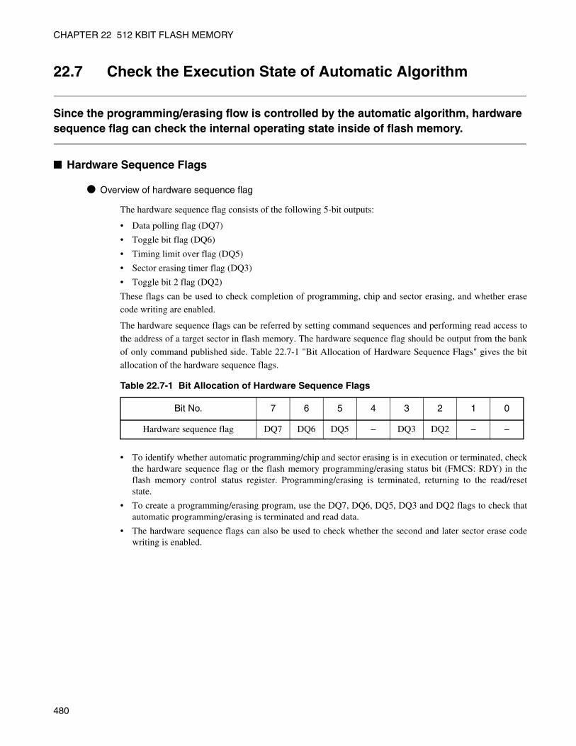
CHAPTER 22 512 KBIT FLASH MEMORY
22.7 Check the Execution State of Automatic Algorithm
Since the programming/erasing flow is controlled by the automatic algorithm, hardware sequence flag can check the internal operating state inside of flash memory.
Hardware Sequence Flags
Overview of hardware sequence flag
The hardware sequence flag consists of the following 5-bit outputs:
• Data polling flag (DQ7)
• Toggle bit flag (DQ6)
• Timing limit over flag (DQ5)
• Sector erasing timer flag (DQ3)
• Toggle bit 2 flag (DQ2)
These flags can be used to check completion of programming, chip and sector erasing, and whether erase
code writing are enabled.
The hardware sequence flags can be referred by setting command sequences and performing read access to
the address of a target sector in flash memory. The hardware sequence flag should be output from the bank
of only command published side. Table 22.7-1 "Bit Allocation of Hardware Sequence Flags" gives the bit
allocation of the hardware sequence flags.
• To identify whether automatic programming/chip and sector erasing is in execution or terminated, checkthe hardware sequence flag or the flash memory programming/erasing status bit (FMCS: RDY) in theflash memory control status register. Programming/erasing is terminated, returning to the read/resetstate.
• To create a programming/erasing program, use the DQ7, DQ6, DQ5, DQ3 and DQ2 flags to check thatautomatic programming/erasing is terminated and read data.
• The hardware sequence flags can also be used to check whether the second and later sector erase codewriting is enabled.
Table 22.7-1 Bit Allocation of Hardware Sequence Flags
Bit No. 7 6 5 4 3 2 1 0
Hardware sequence flag DQ7 DQ6 DQ5 − DQ3 DQ2 − −
480

CHAPTER 22 512 KBIT FLASH MEMORY
Explanation of hardware sequence flag
Table 22.7-2"List of Hardware Sequence Flag Functions" lists the functions of the hardware sequence flag.
Table 22.7-2 List of Hardware Sequence Flag Functions
State DQ7 DQ6 DQ5 DQ3 DQ2
State change in normal
operation
Programming → Completed(when program address specified)
DQ7 → DADATA:7
Toggle →DATA:6
0 → DATA:5
0 → DATA:3
1 → DATA:2
Chip and sector erasing → Completed
0 → 1 Toggle → Stop
0 → 1 1 Toggle → Stop
Sector erasing wait → Started
0 Toggle 0 0 → 1 Toggle
Erasing → Sector erasing suspended(Sector being erased)
0 → 1 Toggle → 1 0 1 → 0 Toggle
Sector erasing suspended → Resumed(Sector being erased)
1 → 0 1 → Toggle 0 0 → 1 Toggle
Sector erasing being suspended(Sector not being erased)
DATA:7 DATA:6 DATA:5 DATA:3 DATA:2
Abnormal operation
Programming DQ7 Toggle 1 0 1
Chip and sector erasing 0 Toggle 1 1 *
*:If the DQ5 flag is 1 (timing limit over), the DQ2 flag performs the toggle operation for continuous reading from the programming/erasing sector but does not perform the toggle operation for reading from other sectors.
481

CHAPTER 22 512 KBIT FLASH MEMORY
22.7.1 Data Polling Flag (DQ7)
The data polling flag (DQ7) is a hardware sequence flag which mainly used to notify that the automatic algorithm is executing or has been completed using the data polling function.
Data Polling Flag (DQ7)Table 22.7-3 and Table 22.7-4 give the state transition of the data polling flag.
At programming
• Read access during execution of the auto-programming algorithm causes flash memory to output thereversed data of bit7 last written.
• Read access at the end of the auto-programming algorithm causes flash memory to output the read valueof bit7 at the address to which read access was performed.
At chip/sector erasing
• During executing chip and sector erasing algorithms, when read access is made to the currently beingerasing sector, bit7 of flash memory outputs 0. When chip erasing/sector erasing is terminated, bit7 offlash memory outputs 1.
Table 22.7-3 State Transition of Data Polling Flag (State Change at Normal Operation)
Operating StateProgramming → Completed
Chip and Sector Erasing → Completed
Wait for Sector Erasing →
Started
Sector Erasing → Erasing Suspended
(Sector being Erased)
Sector Erasing Suspended →
Resume (Sector being
Erased)
Sector Erasing being
Suspended (Sector not
being Erased)
DQ7 DQ7 → DATA:7 0 → 1 0 0 → 1 1 → 0 DATA:7
Table 22.7-4 State Transition of Data Polling (State Change at Abnormal Operation)
Operating State Programming Chip and Sector Erasing
DQ7 DQ7 0
482

CHAPTER 22 512 KBIT FLASH MEMORY
At sector erasing suspension
• Read access during sector erasing suspension causes flash memory to output 1 if the address specifiedby the address signal belongs to the sector being erased. Flash memory outputs bit7 (DATA: 7) of theread value at the address specified by the signal address if the address specified by the address signaldoes not belong to the sector being erased.
• Referring this flag together with the toggle bit flag (DQ6) permits a decision on whether flash memoryis in the erase suspended state and which sector is being erased.
Note:
Read access to the specified address while the automatic algorithm starts is ignored. Data readingcan be enabled after "1" is set to data polling flag (DQ7). Data reading after the end of the automaticalgorithm should be performed following read access after completion of data polling has beenchecked.
483
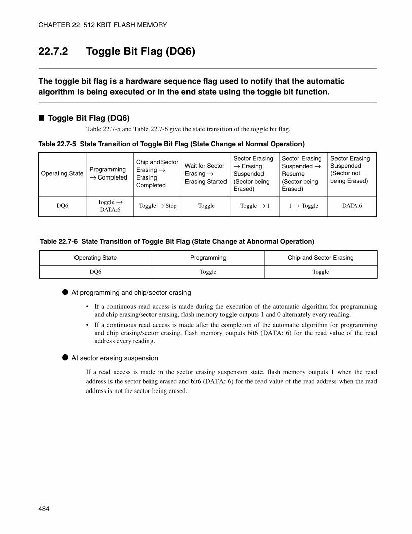
CHAPTER 22 512 KBIT FLASH MEMORY
22.7.2 Toggle Bit Flag (DQ6)
The toggle bit flag is a hardware sequence flag used to notify that the automatic algorithm is being executed or in the end state using the toggle bit function.
Toggle Bit Flag (DQ6)Table 22.7-5 and Table 22.7-6 give the state transition of the toggle bit flag.
At programming and chip/sector erasing
• If a continuous read access is made during the execution of the automatic algorithm for programmingand chip erasing/sector erasing, flash memory toggle-outputs 1 and 0 alternately every reading.
• If a continuous read access is made after the completion of the automatic algorithm for programmingand chip erasing/sector erasing, flash memory outputs bit6 (DATA: 6) for the read value of the readaddress every reading.
At sector erasing suspension
If a read access is made in the sector erasing suspension state, flash memory outputs 1 when the read
address is the sector being erased and bit6 (DATA: 6) for the read value of the read address when the read
address is not the sector being erased.
Table 22.7-5 State Transition of Toggle Bit Flag (State Change at Normal Operation)
Operating StateProgramming → Completed
Chip and Sector Erasing → Erasing Completed
Wait for Sector Erasing → Erasing Started
Sector Erasing → ErasingSuspended (Sector being Erased)
Sector Erasing Suspended → Resume (Sector being Erased)
Sector Erasing Suspended (Sector not being Erased)
DQ6Toggle → DATA:6 Toggle → Stop Toggle Toggle → 1 1 → Toggle DATA:6
Table 22.7-6 State Transition of Toggle Bit Flag (State Change at Abnormal Operation)
Operating State Programming Chip and Sector Erasing
DQ6 Toggle Toggle
484

CHAPTER 22 512 KBIT FLASH MEMORY
22.7.3 Timing Limit Over Flag (DQ5)
The timing limit over flag (DQ5) is a hardware sequence flag that notifies flash memory that the execution of the automatic algorithm has exceeded a prescribed time (the time required for programming/erasing).
Timing Limit Over Flag (DQ5)Table 22.7-7 and Table 22.7-8 give the state transition of the timing limit over flag.
At programming and chip/sector erasing
• If a read access is made after starting the automatic algorithm for programming or chip /sector erasingand it is within a prescribed time (the time required for programming/erasing), the timing limit over flag(DQ5) outputs 0. If it exceeds the prescribed time, the timing limit over flag (DQ5) outputs 1.
• The timing limit over flag (DQ5) can be used to identify the success or failure of programming/erasing,regardless of whether the automatic algorithm is in progress or terminated. If the automatic algorithm bythe data polling or the toggle bit function is in execution when the timing limit over flag (DQ5) outputs1, programming can be identified as a failure.
• For example, when "1" is set to the flash memory address with "1" set the flash memory, programmingfails. In this case, the flash memory will be locked and the automatic algorithm will not complete.Therefore, no valid data is output from the data polling flag (DQ7). Also, the toggle bit flag (DQ6) doesnot stop the toggle operation and exceeds the time limit, causing the timing limit over flag (DQ5) tooutput 1. This state means that the flash memory is not being used correctly; it does not mean that theflash memory is faulty. When this state occurs, execute the reset command.
Table 22.7-7 State Transition of Timing Limit Over Flag (State Change at Normal Operation)
Operating StateProgramming → Completed
Chip and Sector Erasing → Completed
Wait for Sector Erasing → Started
Sector Erasing → Erasing Suspended (Sector being Erased)
Sector Erasing Suspended → Resume (Sector being Erased)
Sector Erasing being Suspended (Sector not being Erased)
DQ5 0 → DATA:5 0 → 1 0 0 0 DATA:5
Table 22.7-8 State Transition of Timing Limit Over Flag (State Change at Abnormal Operation
Operating State Programming Chip and Sector Erasing
DQ5 1 1
485

CHAPTER 22 512 KBIT FLASH MEMORY
22.7.4 Sector Erase Timer Flag (DQ3)
The sector erase timer flag is used to notify during the period of waiting for sector erasing after the sector erase command has started.
Sector Erase Timer Flag (DQ3)Table 22.7-9 and Table 22.7-10 give the state transition of the sector erase timer flag.
At sector erasing
• If a read access is made after starting the sector erase command and it is within a sector erasing waitperiod, the sector erasing timer flag (DQ3) outputs 0. If it exceeds the period, the sector erasing timerflag (DQ3) outputs 1.
• If the sector erasing timer flag (DQ3) is 1, indicating that the automatic algorithm for sector erasing bythe data polling or toggle bit function is in progress (DQ7 = 0; DQ6 produces a toggle output), sectorerasing is performed. If any command other than the sector erasing suspension is set, it is ignored untilsector erasing is terminated.
• If the sector erasing timer flag (DQ3) is 0, flash memory can accept the sector erase command. Toprogram the sector erase command, check that the sector erasing timer flag (DQ3) is 0. If the flag is 1,flash memory may not accept the sector erase command of suspending.
At sector erasing suspension
• Read access during sector erasing suspension causes flash memory to output 1, if the read address is inthe sector being erased. Flash memory outputs bit3 (DATA: 3) for the read value of the read addresswhen the read address is not the sector being erased.
Table 22.7-9 State Transition of Sector Erase Timer Flag (State Change at Normal Operation)
Operating StateProgramming → Completed
Chip and Sector Erasing → Completed
Wait for Sector Erasing → Started
Sector Erasing → Erasing Suspended (Sector being Erased)
Sector Erasing Suspended → Resume (Sector being Erased)
Sector Erasing being Suspended (Sector not being Erased)
DQ3 0 → DATA3 1 0 → 1 1 → 0 0 → 1 DATA:3
Table 22.7-10 State Transition of Sector Erase Timer Flag (State Change at Abnormal Operation)
Operating State Programming Chip and Sector Erasing
DQ3 0 1
486

CHAPTER 22 512 KBIT FLASH MEMORY
22.7.5 Toggle Bit 2 Flag (DQ2)
The toggle bit 2 flag (DQ2) is a hardware sequence flag that notifies flash memory that sector erasing is being suspended using the toggle bit function.
Toggle Bit Flag (DQ2)Table 22.7-11 and Table 22.7-12 give the state transition of the toggle bit flag.
At sector erasing
• If a continuous read access is made during the execution of the automatic algorithm for chip /sectorerasing, flash memory toggle-outputs 1 and 0 alternately every reading.
• If a continuous read access is made after the completion of the algorithm for chip/sector erasing, flashmemory outputs bit2 (DATA: 2) of the read address every reading.
Table 22.7-11 State Transition of Toggle Bit Flag (State Change at Normal Operation)
Operating StateProgramming → Completed
Chip and Sector Erasing → Completed
Wait for Sector → Started
Sector Erasing → Erasing Suspended (Sector being Erased)
Sector Erasing Suspended → Resume Sector being Erased)
Sector Erasing being Suspended (Sector not being Erased)
DQ2 1 → DATA:2 Toggle → Stop Toggle Toggle Toggle DATA:2
Table 22.7-12 State Transition of Toggle Bit Flag (State Change at Abnormal Operation)
Operating State Programming Chip and Sector Erasing
DQ2 1 *
*:If the DQ5 flag is 1 (timing limit over), the DQ2 flag performs the toggle operation for continuous reading from the programming/erasing sector but does not perform the toggle operation for reading from other sectors.
487

CHAPTER 22 512 KBIT FLASH MEMORY
At sector erasing suspension
• If a continuous read access is made in the state of the sector erasing suspension, flash memory outputs 1and 0 alternately when the read address is the sector being erased and bit2 (DATA: 2) for the read valueof the read address when the read address is not the sector being erased.
• If programming is performed in the state of the sector erasing suspension, flash memory outputs 1 whena continuous read access is started with the sector that is not in the state of the sector erasing suspension.
• The toggle bit 2 flag (DQ2) is used together with the toggle bit flag (DQ6) to detect that sector erasing issuspended (the DQ2 flag performs the toggle operation but the DQ6 flag does not).
• If a read access to the sector being erased is made, the toggle bit 2 flag (DQ2) performs the toggleoperation, so it can also be used to detect the sector being erased.
488

CHAPTER 22 512 KBIT FLASH MEMORY
22.8 Details of Programming/Erasing Flash Memory
This section explains the procedure for inputting commands starting the automatic algorithm, and for read/reset of flash memory, programming, chip erasing, sector erasing, sector erasing suspension and sector erasing resumption.
Detailed Explanation of Programming and Erasing Flash MemoryThe automatic algorithm can be started by programming the command sequence of read/reset,
programming, chip erasing, sector erasing, sector erasing suspension and erasing resumption from CPU to
flash memory. Programming flash memory from the CPU should always be performed continuously. The
termination of the automatic algorithm can be checked by the data polling function. After normal
termination, it returns to the read/reset state.
Each operation is explained in the following order.
• Read/reset state
• Data programming
• All data erasing (chip all erase)
• Any data erasing (sector erase)
• Sector erasing suspension
• Sector erasing resumption
489

CHAPTER 22 512 KBIT FLASH MEMORY
22.8.1 Read/Reset State in Flash Memory
This section explains the procedure for inputting the read/reset command to place flash memory in the read/reset state.
Read/Reset State in Flash Memory• Flash memory can be placed in the read/reset state by transmitting the read/reset command in the
command sequence table from CPU to flash memory.
• There are two kinds of read/reset commands: one is executed at one time bus operation, and the other isexecuted at three times bus operation; the command sequence of both is essentially the same.
• Since the read/reset state is the initial state for flash memory, flash memory always enters this state afterpower-on and at the normal termination of command. The read/reset state is also described as the waitstate for command input.
• In the read/reset state, a read access to flash memory enables data to be read. As is the case with maskROM, a program access from the CPU can be made.
• A read access to flash memory does not require the read/reset command. If the command is notterminated normally, use the read/reset command to initialize the automatic algorithm.
490

CHAPTER 22 512 KBIT FLASH MEMORY
22.8.2 Data Programming to Flash Memory
This section explains the procedure for inputting the program command to program data to flash memory.
Data Programming to Flash Memory• In order to start the data programming automatic algorithm, continuously transmit the program
command in the command sequence table from CPU to flash memory.
• At completion of data programming to a target address in the fourth cycle, the automatic algorithm startsautomatic programming.
How to specify address
• Only even addresses can be specified for the programming address specified by programming datacycle. Specifying odd addresses prevents correct writing. Writing to even addresses must be performedin word data units.
• Programming is possible in any address order or even beyond sector boundaries. However, execution ofone programming command permits programming of data for only one word.
Notes on data programming
• The bit data 0 cannot be returned to the bit data 1 by programming. When the bit data 0 is programmedto data 1, the data polling algorithm (DQ7) or toggling (DQ6) is not terminated and the flash memory isconsidered faulty; the timing limit over flag (DQ5) is determined as an error.
• When data is read in the read/reset state, the bit data remains 0. To return the bit data to 1 from 0, eraseflash memory data.
• All commands are ignored during automatic programming.
• If a hardware reset occurs during programming, data being programmed to addresses is not assured.Please re-try from chip delete or sector erase.
Data Programming Procedure• Figure 22.8-1 gives an example of the procedure for programming data into flash memory. The
hardware sequence flags can be used to check the operating state of the automatic algorithm in flashmemory. The data polling flag (DQ7) is used for checking the completion of programming to flashmemory in this example.
• Flag check data should be read from the address where data was last written.
• Because the data polling flag (DQ7) and the timing limit over flag (DQ5) change at the same time, thedata polling flag (DQ7) must be checked even when the timing limit over flag (DQ5) is 1.
• Similarly, since the toggle bit flag (DQ6) stops toggling at the same time the timing limit over flag(DQ5) changes to 1, the toggle bit flag (DQ6) must be checked.
491

CHAPTER 22 512 KBIT FLASH MEMORY
Figure 22.8-1 Example of Data Programming Procedure
Start
Internal address read
Program command sequence(1)FFUAAA XXAA(2)FFU554 XX55(3)FFUAAA XXA0(4)Program address Program data
Next address
FMCS: WE (bit5)Programming enabled
FFWR0/1Accidental write preventive function setting(Accidental write preventive sector: 0, writing sector :1 )
Data polling(DQ7)
Data
Data
Timing limit(DQ5)
1
0
Last address
YES
NO
FMCS: WE (bit5)Programming enabled
Data
Data
Internal address read
Data polling(DQ7)
Programming error
Completed
492

CHAPTER 22 512 KBIT FLASH MEMORY
22.8.3 Data Erase from Flash Memory (Chip Erase)
This section explains the procedure for inputting the chip erase command to erase all data from flash memory.
All Data Erase from Flash Memory (Chip Erase)• All data can be erased from flash memory by continuously transmitting the chip erase command in the
command sequence table from CPU to flash memory.
• The chip erase command is executed in six bus operations. Chip erasing is started at completion of thesixth programming cycle.
• Before chip erasing, the user need not perform programming to flash memory. During execution of theautomatic erasing algorithm, flash memory automatically programs 0 before erasing all cells.
Notes on Chip Erasure• The chip erase command is accepted only when all sectors have been write-enabled. The chip erase
command is ignored when any of the sector write-enable/protect bits in the flash memory write controlregister (FWR0/1) contains "0" (write-protected or accidental write prevented status).
• If the hardware reset is generated during erase operation, the data of flash memory is not guaranteed.
493
CHAPTER 22 512 KBIT FLASH MEMORY
22.8.4 Erasing Any Data in Flash Memory (Sector Erasing)
This section explains the procedure for inputting the sector erase command to erase any data in flash memory. Sector-by-sector erasing is enabled and multiple sectors can be specified at the same time.
Erasing Any Data in Flash Memory (Sector Erasing)Any sector in flash memory can be erased by continuously transmitting the sector erase command in the
command sequence table from CPU to flash memory.
How to specify sector
• The sector erase command is executed in six bus operations. By setting the address on the sixth cycle onthe even address in the target sector and programming the sector erase code (30H) to data, a 50 µs sectorerasing wait is started
• When erasing more than one sector, the sector erase code (30H) is programmed to the sector address tobe erased, following the above.
Notes on specifying multiple sectors
• Sector erasing is started after a 50 µs period waiting for sector erasing is completed after the last sectorerase code has been programmed.
• That is, when erasing more than one sector simultaneously, the address of erase sector address and thesector code must be input within 50 µs. If the sector erase code is input 50 µs or later, it cannot beaccepted.
• Whether continuous programming of the sector erase code is enabled can be checked by the sector erasetimer flag (DQ3).
• In this case, the address from which the sector erase timer flag (DQ3) is read should correspond to thesector to be erased.
Erasing Procedure for Flash Memory Sectors• The state of the automatic algorithm in the flash memory can be determined using the hardware
sequence flag. Figure 22.8-2 gives an example of the flash memory sector erase procedure. In thisexample, the toggle bit flag (DQ6) is used to check that erase ends.
• DQ6 terminates toggling concurrently with the change of the timing limit over flag (DQ5) to "1", so theDQ6 must be checked even when DQ5 is "1".
• Similarly, the data polling flag (DQ7) changes concurrently with the transition of the DQ5, so DQ7must be checked.
Note on Sector Erasing• If the hardware reset is generated during erase operation, the data of flash memory is not guaranteed.
Please re-try sector erase.
494

CHAPTER 22 512 KBIT FLASH MEMORY
Figure 22.8-2 Example of Sector Erasing Procedure
Start
(6) Code input to erase sector (30H)
Erase command sequence(1) FFAAAA XXAA(2) FF5554 XX55(3) FFAAAA XX80(4) FFAAAA XXAA(5) FF5554 XX55
Next sector
Internal address read
Internal address read
Is any other erase sector?
Timing limit(DQ5)
1
Completed
0
Last sector
FMCS : WE (bit 5)Programming enabled
Erasing error
Internal address read
Sector erase timer(DQ3)
1
0
Internal address read 2
Internal address read 1
Toggle bit (DQ6)Data 1 = Data 2
Toggle bit (DQ6)Data 1 = Data 2
NO
NO
NO
NO
YES
YES
YES
YES
FFWR0/1Accidental write preventive function setting(Accidental write preventive sector: 0, writing sector :1 )
FMCS: WE (bit5)Programming enabled
495

CHAPTER 22 512 KBIT FLASH MEMORY
22.8.5 Sector Erase Suspension
This section explains the procedure for inputting the sector erase suspend command to suspend sector erasing. Data can be read from the sector not being erased.
Sector Erase Suspension• To cause flash memory sector erasing to suspend, transmit the sector erasing suspend command in the
command sequence table from CPU to flash memory.
• The sector erasing suspend command suspends the sector erase currently being performed, enabling dataread from a sector that is currently not being erased.
• This command is only enabled during the sector erasing period including the erasing wait time; it isignored during the chip erasing period or during programming.
• The sector erasing suspend command is executed when the sector erasing suspend code (B0H) isprogrammed. Arbitrary address in flash memory should be set for address. If the sector erasing suspendcommand is executed during sector erasing pause, the successive command input is ignored.
• When the sector erasing suspend command is input during the sector erasing wait period, the sectorerase wait state ends immediately, the erasing is interrupted, and the erase stop state occurs.
• When the erase suspend command is input during the sector erasing after the sector erase wait period,the erase suspend state occurs after a maximum of 20 µs.
NoteTo issue the suspension command, please issue the command after the following; 20 µs after the sector
erase command issue, or 20 µs after the sector erasing resumption command issue. However, please make
the issue number of times within several-time.
496

CHAPTER 22 512 KBIT FLASH MEMORY
22.8.6 Sector Erase Resumption
This section explains the procedure for inputting the sector erase resume command to resume erasing of the suspended flash memory sector.
Erase Resumption• Suspended sector erasing can be resumed by transmitting the sector erase resume command in the
command sequence table from CPU to flash memory.
• The sector erase resume command resumes sector erasing suspended by the sector erase suspendcommand. This command is executed by writing the erase resume code (30H). In this case, even addressin the specified sector for erase area is specified.
• Inputting the sector erase resume command during sector erasing is ignored.
497

CHAPTER 22 512 KBIT FLASH MEMORY
498

CHAPTER 23DUAL OPERATION FLASH
This chapter describes the functions and operation of Dual Operation Flash.
23.1 Overview of Dual Operation Flash
23.2 Register for Dual Operation Flash
23.3 Operation of Dual Operation Flash
499

CHAPTER 23 DUAL OPERATION FLASH
23.1 Overview of Dual Operation Flash
Dual Operation Flash consists of the upper bank (16 K bytes 2 + 4 K bytes 4) and lower bank (4 K bytes 4), allowing concurrent execution of an erase/program and a read in the two banks, which is not allowed in conventional flash products. This feature enables program execution in the flash memory and programming control using interrupts. It also eliminates the need for a conventional process to download a program to RAM for execution to program data into the flash memory, resulting in reduced download time and no need to consider power shutdown for RAM data maintenance.Also, the minimum sectors are as compact as four kilobytes that can be handled easily as program/data areas.
Features of Dual Operation Flash• Tow-bank configuration, enabling simultaneous execution of an erase/program and reading
• Minimum sectors in four kilobytes to be handled easily as program/data areas
In the Dual Operation Flash, the following combination is possible.
Upper bank Lower bank
Read
Read Write/Sector eras
Write/Sector erase Read
Chip erase
Note: When one bank is in state of write/sector erase, the other bank cannot use it.
500

CHAPTER 23 DUAL OPERATION FLASH
23.2 Register for Dual Operation Flash
The following register is used for operation of Dual Operation Flash: • Sector switching register (SSR0)
Sector Switching Register (SSR0)Figure 23.2-1 shows the configuration of the sector switching register (SSR0).
Please use byte access for write/read to the sector switching register.
Figure 23.2-1 The Configuration of the Sector Switching Register (SSR0)
Table 23.2-1 The Function of the Sector Switching Register (SSR0)
Bit name Function
bit7, bit6 Reserved: Reserved bit Be sure to set to "0".
bit5 to bit1 Undefined bitAt a read: The value is undefined.At a write: The operation is not affected.
bit0 SEN0:
The SEN0 bit switches access from the CPU for reprogramming the upper bank from SA9 containing the interrupt vector to SA3 in the lower bank.
bit 7
R/W
- - - - - SEN0
6
R/W
5 4 3 2 1 0
R/W(0) (0) (X) (X) (X) (X) (X) (0)
R/W : Read/Write enabled
SSR0
[00790EH] Reserved Reserved
SEN001
FunctionInterrupt vector to SA9 (Initial value)
Interrupt vector to SA3
501

CHAPTER 23 DUAL OPERATION FLASH
SEN0 Bit access Sector MapFigure 23.2-2 shows the access sector map based on the SEN0 setting.
Figure 23.2-2 The access Sector Map Based on the SEN0 Setting
FF0000H
FF0FFFHFF1000H
FF1FFFHFF2000H
FF2FFFHFF3000H
FF3FFFHFF4000H
FF7FFFHFF8000H
FFBFFFHFFC000H
FFCFFFHFFD000H
FFDFFFHFFE000H
FFEFFFHFFF000H
FFFFFFH
SA0:4K
SA1:4K
SA2:4K
SA3:4K
SA4:16K
SA5:16K
SA6:4K
SA7:4K
SA8:4K
SA9:4K
SA0:4K
SA1:4K
SA2:4K
SA9:4K
SA4:16K
SA5:16K
SA6:4K
SA7:4K
SA8:4K
SA3:4K
Hard Wired Reset Vector(FFE000H)
Interrupt Vector
CPU address
SEN0=0 SEN0=1
Interrupt Vector
Upp
er B
ank
Low
er B
ank
502

CHAPTER 23 DUAL OPERATION FLASH
23.3 Operation of Dual Operation Flash
Described below is the operation of Dual Operation Flash.Pay particular attention to the following points when using Dual Operation Flash: • Interrupt occurring when the upper bank is reprogrammed• Sector switching register (SSR0) setting procedure
Interrupt Occurring when the Upper Bank is ReprogrammedDual Operation Flash consists of two banks and, like conventional flash memory products, it cannot
execute an erase/program and a read simultaneously in the same bank.
Since SA9 contains an interrupt vector, the interrupt vector from the CPU cannot be read normally when an
interrupt occurs at write access to the upper bank. To reprogram the upper bank, SSR0:SEN0 must be set to
"1". When an interrupt occurs, therefore, SA3 is accessed to read the interrupt vector data. The same data as
SA3 and SA9 must be before setting the sector switching register (SSR0).
Sector Switching Register (SSR0) Setting ProcedureFigure23.3-1 illustrates the procedure of setting the sector switching register (SSR0).
The SEN0 bit must be set to "1" before reprogramming of data in the upper bank. Note also that it is not
allowed to make any change to the setting of the sector switching register (SSR0) during write access to the
flash memory. Be sure to set the sector switching register (SSR0) before or after reprogramming the flash
memory.
During setting this register, the interrupt enable is set prohibit. After setting SEN0 bit, the interrupt will be
set enable.
Figure23.3-1 The Procedure of Setting the Sector Switching Register (SSR0)
Start of FLASH data reprogramming
Copy SA9 data to SA3
SSR0: SEN0 setting ("1")
Start of FLASH data writing
End of FLASH data reprogramming
End of FLASH data reprogramming
Start of FLASH data writing
SSR0: SEN0 setting ("0")
503

CHAPTER 23 DUAL OPERATION FLASH
Operation during Write/Erase• If the interrupt is generated during write/erase to flash memory, the write/erase operation to flash
memory is prohibited in interrupt routine.
If there are two or more write/erase routines, the next write/erase routine should be execution after the
an write/erase routine step-by-step.
• During write/erase operation to flash memory, the state transferring from write/erase mode (main clock
mode, PLL clock mode, sub clock mode) is prohibited.
The state transfers after write/erase operation.
504

CHAPTER 24EXAMPLE of CONNECTING
SERIAL WRITING
This chapter describes examples of serial write connection when using AF220/AF210/AF120/AF110 flash microcontroller programmer made by Yokogawa Digital Computer Corporation.
24.1 Basic Configuration
24.2 Oscillation Clock Frequency and Serial Clock Input Frequency
24.3 Flash Microcomputer Programmer System Configuration
24.4 Example of Connecting Serial Writing
505

CHAPTER 24 EXAMPLE of CONNECTING SERIAL WRITING
24.1 Basic Configuration
The MB90F337 supports the serial on-board programming of flash ROM (Fujitsu standard). The specification for serial on-board programming are explained below.
The Serial on Board Writing Basic ComponentThe flash microcontroller programmer made by Yokogawa Digital Computer Corporation is used for
Fujitsu standard serial on-board programming.
Figure 24.1-1 shows the basic configuration of serial write connection examples.
Figure 24.1-1 Basic Configuration of Example for Serial Write Connection
Note:
Contact Yokogawa Digital Computer Corporation for details of the functions, operations, general-purpose common connecting cable (AZ210) and applicable connectors of the flash microcontrollerprogrammer AF220/AF210/AF120/AF110.
MB90F337
Host interface cable (AZ201) General-purpose common connecting cable (AZ201)
User system
Flash microcontrollerprogrammer
Memory card
CLKsynchronous serial
Stand-alone operation enabled
RS232C
506

CHAPTER 24 EXAMPLE of CONNECTING SERIAL WRITING
Pins Used for Fujitsu Standard Serial On-board ProgrammingTable 24.1-1 shows the function of pins used for Fujitsu standard serial on-board programming.
Figure 24.1-2 Pin Control Circuit
Notes:
• When the P60, P61, SIN0, SOT0, or SCK0 pin is used also in a user system, the control circuitshown in Figure 24.1-2 is required.
• During serial write, the user circuit can be disconnected using the /TICS signal from the flashmicrocontroller programmer. Please refer to "24.4 Example of Connecting Serial Writing".
Table 24.1-1 Function of Used Pins
Pin Function Supplementary Information
MD2,MD1,MD0 Mode PinSetting MD2=1, MD1=1, and MD0=0 allows the mode to be in the serial write mode.
X0,X1 Oscillation pins
Because the internal CPU operation clock is set to be the 1 multiplication PLL clock in the serial write mode, the internal operation clock frequency is the same as the oscillation clock frequency. When you perform the serial write, the frequency you can input into the high-speed oscillation input terminal is fixed to 6 MHz.
P60,P61 Writing program activating pins
Input a Low level to P60 and a "H" level to P61.
RST Reset -
SIN0 Serial data input
UART0 is used as CLK synchronous mode.SOT0 Serial data output
SCK0 Serial clock input
VCC Supply voltage Supply the write voltage (VCC=3.3 V ± 0.3 V)
VSS GND GND pin is common to the ground of the flash microcontroller programmer.
MB90F337Write control pin Write control pin
/TICS pin
User
10 kΩ
AF220/AF210/AF120/AF110
AF220/AF210/AF120/AF110
507

CHAPTER 24 EXAMPLE of CONNECTING SERIAL WRITING
24.2 Oscillation Clock Frequency and Serial Clock Input Frequency
The MB90F337 serial clock frequency that can be input is determined by the following expression:Thus, set up the flash microcontroller programmer to change the serial clock input frequency corresponding to the using oscillation clock frequency.
Oscillation Clock Frequency and Serial Clock Input FrequencySerial clock frequencies that can be input are determined using the expression below.
Inputable serial clock frequency = 0.125 x oscillation clock frequency.
Table 24.2-1 shows the serial clock frequencies that can be input.
Table 24.2-1 Serial Clock Frequency that can be Input
Oscillation clock frequency
Maximum serial clock frequency that can be input to the microcomputer
Maximum serial clock frequency that can be set with AF220, AF210, AF120, or AF110
Maximum serial clock frequency that can be set with AF200
in 6 MHz 750 kHz 500 kHz 500 kHz
508
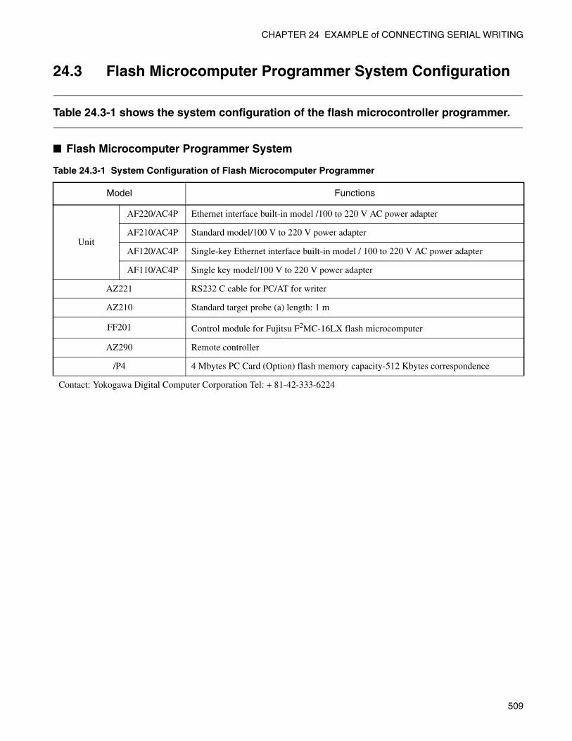
CHAPTER 24 EXAMPLE of CONNECTING SERIAL WRITING
24.3 Flash Microcomputer Programmer System Configuration
Table 24.3-1 shows the system configuration of the flash microcontroller programmer.
Flash Microcomputer Programmer System
Table 24.3-1 System Configuration of Flash Microcomputer Programmer
Model Functions
Unit
AF220/AC4P Ethernet interface built-in model /100 to 220 V AC power adapter
AF210/AC4P Standard model/100 V to 220 V power adapter
AF120/AC4P Single-key Ethernet interface built-in model / 100 to 220 V AC power adapter
AF110/AC4P Single key model/100 V to 220 V power adapter
AZ221 RS232 C cable for PC/AT for writer
AZ210 Standard target probe (a) length: 1 m
FF201 Control module for Fujitsu F2MC-16LX flash microcomputer
AZ290 Remote controller
/P4 4 Mbytes PC Card (Option) flash memory capacity-512 Kbytes correspondence
Contact: Yokogawa Digital Computer Corporation Tel: + 81-42-333-6224
509

CHAPTER 24 EXAMPLE of CONNECTING SERIAL WRITING
24.4 Example of Connecting Serial Writing
The examples of serial write connection is shown below.
Example of Connecting Serial WritingExample of connecting serial writing has following two types.
• Connection example in Single-chip mode (when using user power)
• Example of minimum connection to flash microcomputer programmer (when using user power)
510
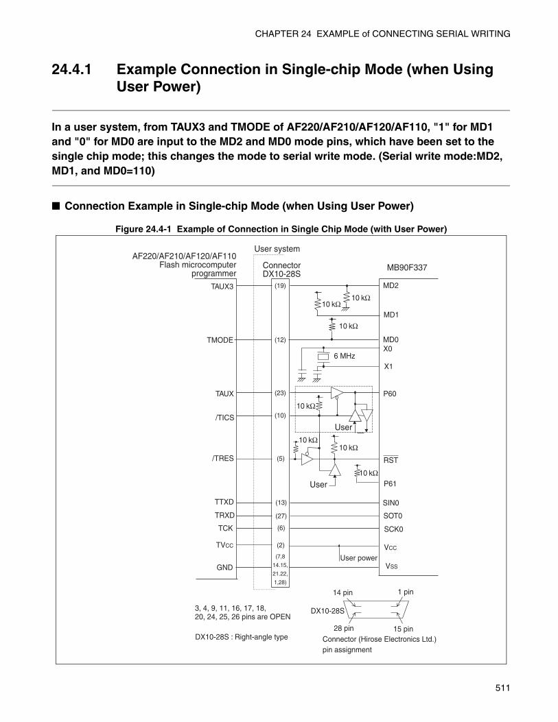
CHAPTER 24 EXAMPLE of CONNECTING SERIAL WRITING
24.4.1 Example Connection in Single-chip Mode (when Using User Power)
In a user system, from TAUX3 and TMODE of AF220/AF210/AF120/AF110, "1" for MD1 and "0" for MD0 are input to the MD2 and MD0 mode pins, which have been set to the single chip mode; this changes the mode to serial write mode. (Serial write mode:MD2, MD1, and MD0=110)
Connection Example in Single-chip Mode (when Using User Power)
Figure 24.4-1 Example of Connection in Single Chip Mode (with User Power)
MB90F337
User systemAF220/AF210/AF120/AF110
Flash microcomputerprogrammer
ConnectorDX10-28S
User
User
User power
14 pin 1 pin
15 pin28 pin
3, 4, 9, 11, 16, 17, 18,20, 24, 25, 26 pins are OPEN
DX10-28S : Right-angle type Connector (Hirose Electronics Ltd.)pin assignment
TAUX3
(23)
(12)
(19)
(10)
(5)
(13)
(27)
(6)
(2)
(7,8
14.15,
21.22,
1,28)
10 kΩ10 kΩ
10 kΩ
10 kΩ
10 kΩ10 kΩ
10 kΩ
TMODE
TAUX
/TICS
/TRES
TTXD
TRXD
TCK
TVCC
GND
6 MHz
MD2
MD1
MD0X0
X1
P60
RST
P61
SIN0
SOT0
SCK0
VCC
VSS
DX10-28S
511

CHAPTER 24 EXAMPLE of CONNECTING SERIAL WRITING
Notes:
• When the SIN0, SOT0, or SCK0 pin is used also in a user system, the control circuit shownin Figure 24.1-2 is required like P60. (During serial write, the user circuit can be disconnectedusing the /TICS signal from the flash microcomputer programmer.)
• Connect the AF220/AF210/AF120/AF110 while the user power is off.
512

CHAPTER 24 EXAMPLE of CONNECTING SERIAL WRITING
24.4.2 Example of Minimum Connection to Flash Microcomputer Programmer (when Using User Power)
During serial write, when MD2, MD0, and P60 pins are set as shown in Figure 24.4-2, it is unnecessary to connect these pins with the flash microcomputer programmer.
Example of Minimum Connection to Flash Microcomputer Programmer (when Using User Power)
Figure 24.4-2 Example of Minimum Connection to Flash Microcomputer Programmer (when Using User Power)
MB90F337
User systemFlash microcomputer
programmer
Connector
User circuit
User circuit
User power
14 pin 1 pin
15 pin28 pinpins are OPEN
At rewriting serial 1
At rewritingserial 1
At rewriting serial 1
At rewriting serial 0
At rewriting serial 0
Pin assignment by connector (Hirose Electronics Ltd.)
AF220/AF210/AF120/AF110
MD2
MD1
MD0
X0
X1
P60
P61
RSTSIN0SOT0
SCK0
Vcc
Vss
DX10-28S
DX10-28S : Right-angle type
3, 4,9, 10, 11, 12, 16, 17,18, 19, 20, 23, 24, 25, 16
DX10-28S
(5)(13)
(27)(6)(2)
(7, 8,14, 15,21, 22,1, 28)
/TRESTTXDTRXD
TCKTVcc
GND
10 kΩ
10 kΩ
10 kΩ
10 kΩ
10 kΩ 10 kΩ
10 kΩ
10 kΩ
6 MHz
10 kΩ
513

CHAPTER 24 EXAMPLE of CONNECTING SERIAL WRITING
Notes:
• When the SIN0, SOT0, or SCK0 pin is used also in a user system, the control circuit shownin Figure 24.1-2 is required. (During serial write, the user circuit can be disconnected using the /TICS signal from the flash microcomputer programmer.)
• Connect the AF220/AF210/AF120/AF110 while the user power is off.
514

APPENDIX
The appendix describes the memory map and the
instructions used in the F2MC-16LX.
APPENDIX A Memory Map
APPENDIX B Instructions
515

APPENDIX
APPENDIX A Memory Map
The memory space divides into three modes.
Memory Map
Figure A-1 Memory Map of MB90335 Series
FFFFFFH
00FFFFH
007FFFH
007900H
007100H
008000H
FF0000H
000100H
0000FBH
000000H
FFFFFFH
00FFFFH
007FFFH
007900H
001100H
008000H
FF0000H
000100H
0000FBH
000000H
FFFFFFH
00FFFFH
007FFFH
007900H
001100H
008000H
FF0000H
000100H
0000FBH
000000H
MB90V330A MB90F337 MB90337
Single chip mode (with ROM mirror function)
Peripheral area
ROM (FF bank)
ROM area(image of FF bank)
Register
RAM area (28 KB)
Peripheral area
Peripheral area
ROM (FF bank)
ROM area(image of FF bank)
Register
RAM area (4 KB)
Peripheral area
Peripheral area
ROM (FF bank)
ROM area(image of FF bank)
Register
RAM area (4 KB)
Peripheral area
516

APPENDIX A Memory Map
Notes:
• When the ROM mirror function register has been set, the mirror image data at higher addresses(“FF8000H to FFFFFFH”) of bank FF is visible from the higher addresses (“008000H to 00FFFFH”)of bank 00.
• For setting the ROM mirror function, see "20. ROM mirror function selection module" in " PERIPHERAL RESOURCES".
References:
• The ROM mirror function is for using the C compiler small model.
• The lower 16-bit addresses of bank FF are equivalent to those of bank 00. Since the ROM area inbank FF exceeds 48 Kbytes, however, the mirror image of all the data in the ROM area cannot bereproduced in bank 00.
• When the C compiler small model is used, the data table mirror image can be shown at "008000Hto 00FFFFH" by storing the data table at "FF8000H to FFFFFFH". Therefore, data tables in theROM area can be referred without declaring the far addressing with the pointer.
517

APPENDIX
I/O MapTable A-1 lists addresses assigned to registers of each peripheral function.
Table A-1 I/O Map (1/8)
Address Registers Abbreviation Access Release Initial value
000000H Port 0 data register PDR0 R/W Port 0 XXXXXXXXB
000001H Port 1 data register PDR1 R/W Port 1 XXXXXXXXB
000002H Port 2 data register PDR2 R/W Port 2 XXXXXXXXB
000003H Use prohibited
000004H Port 4 data register PDR4 R/W Port 4 XXXXXXXXB
000005H Port 5 data register PDR5 R/W Port 5 ---XXXXXB
000006H Port 6 data register PDR6 R/W Port 6 XXXXXXXXB
000007H to
00000FH
Use prohibited
000010H Port 0 data direction register DDR0 R/W Port 0 00000000B
000011H Port 1 direction register DDR1 R/W Port 1 00000000B
000012H Port 2 direction register DDR2 R/W Port 2 00000000B
000013H Use prohibited
000014H Port 4 direction register DDR4 R/W Port 4 00000000B
000015H Port 5 direction register DDR5 R/W Port 5 ---00000B
000016H Port 6 direction register DDR6 R/W Port 6 00000000B
000017H to
00001AH
Use prohibited
00001BH Port 4 output terminal register ODR4 R/W Port 4 (OD
control) 00000000B
00001CH Port 0 Pull-up resistance register RDR0 R/W Port 0(PULLUP) 00000000B
00001DH Port 1 Pull-up resistance register RDR1 R/W Port 1(PULLUP) 00000000B
00001EH, 00001FH
Use prohibited
000020H Serial mode register 1 SMR0 R/W
UART0
00100000B
000021H Serial control register 0 SCR0 R/W,W 00000100B
000022HSerial input data register 0/serial output data register 0
SIDR0/ SODR0 R/W XXXXXXXXB
000023H Serial Status Register 0 SSR0 R/W,R 00001000B
000024H UART prescaler reload register 0 UTRLR0 R/W Communication Prescaler (UART0)
00000000B
000025H UART prescaler control register 0 UTCR0 R/W 0000-000B
518

APPENDIX A Memory Map
000026H Serial mode register 1 SMR1 R/W
UART1
00100000B
000027H Serial control register 1 SCR1 R/W,W 00000100B
000028HSerial input data register 1/serial output data register 1
SIDR1/ SODR1 R/W XXXXXXXXB
000029H Serial status register 1 SSR1 R/W,R 00001000B
00002AH UART prescaler reload register 1 UTRLR1 R/W Communication Prescaler (UART1)
00000000B
00002BH UART prescaler control register 1 UTCR1 R/W 0000-000B
00002CH to
00003BH
Use prohibited
00003CH DTP/interruption permission register ENIR R/W
DTP/external interrupt
00000000B
00003DH DTP/interruption factor register EIRR R/W 00000000B
00003EHRequest level set register subordinate position ELVR
R/W 00000000B
00003FH High rank of request level set register R/W 00000000B
000040H to
000045H
Use prohibited
000046H PPG0 operation mode control register PPGC0 R/W PPG ch.0 0X000XX1B
000047H PPG1 operation mode control register PPGC1 R/W PPG ch.1 0X000001B
000048H PPG2 operation mode control register PPGC2 R/W PPG ch.2 0X000XX1B
000049H PPG3 operation mode control register PPGC3 R/W PPG ch.3 0X000001B
00004AHUse prohibited
00004BH
00004CH PPG0,1 output control register PPG01 R/W PPG ch.0/1 000000XXB
00004DH Use prohibited
00004EH PPG2,3 output control register PPG23 R/W PPG ch.2/3 000000XXB
00004FH to
000057H
Use prohibited
000058HSerial mode control status register SMCS R/W
I/O Extended serial
XXXX0000B
000059H 00000010B
00005AH Serial data register SDR R/W XXXXXXXXB
00005BH Communication Prescaler Control Register SDCR R/W Communication
Prescaler0XXX0000B
Table A-1 I/O Map (2/8)
Address Registers Abbreviation Access Release Initial value
519

APPENDIX
00005CHPWC Control Status Registers PWCSR R/W,R
16-bit PWC timer
00000000B
00005DH 0000000XB
00005EHPWC data buffer register PWCR R/W
00000000B
00005FH 00000000B
000060H PWC ratio of dividing frequency control register DIVR R/W ------00B
000061H Use prohibited
000062HTimer control status register 0 TMCSR0 R/W
16bit reload timer ch.0
00000000B
000063H XXXX0000B
000064HLow order of 16-bit timer register 0 TMR0 R XXXXXXXXB
Low order of 16-bit reloading 0 TMRLR0 W XXXXXXXXB
000065HHigh order of 16-bit timer register 0 TMR0 R XXXXXXXXB
High order of 16-bit reloading 0 TMRLR0 W XXXXXXXXB
000066H to
00006EH
Use prohibited
00006FH ROM Mirroring Function Select Register ROMM R/W, WROM mirror
function------11B
000070H I2C bus status register 0 IBSR0 R
I2C interface ch.0
00000000B
000071H I2C bus control register 0 IBCR0 R/W 00000000B
000072H I2C bus clock control register 0 ICCR0 R/W XX0XXXXXB
000073H I2C bus address register 0 IADR0 R/W XXXXXXXXB
000074H I2C bus data register 0 IDAR0 R/W XXXXXXXXB
000075H to
00009AH
Use prohibited
00009BHDMA descriptor channel specification register
DCSR R/W
µDMAC
00000000B
00009CH Low order of DMA status register DSRL R/W 00000000B
00009DH Low order of DMA status register DSRH R/W 00000000B
00009EHProgram address detection control status register
PACSR R/W Address compare
detection00000000B
00009FHDelay interruption factor generation/release register
DIRR R/W Delayed interrupt -------0B
0000A0HLow-power consumption mode control register
LPMCR R/W, WLow power
consumption00011000B
0000A1H Clock select register CKSCR R/W, R Clock 11111100B
0000A2H to
0000A3H
Use prohibited
0000A4H DMA stop status register DSSR R/W µDMAC 00000000B
Table A-1 I/O Map (3/8)
Address Registers Abbreviation Access Release Initial value
520

APPENDIX A Memory Map
0000A5H to
0000A7H
Use prohibited
0000A8H Watchdog timer control register WDTC R, W Watchdog
TimersX-XXX111B
0000A9H Timebase timer control register TBTC R/W, WTimebase
Timers1--00100B
0000AAH,
0000ABHUse prohibited
0000ACH Low order of DMA permission register DERL R/W µDMAC
00000000B
0000ADH High order of DMA permission register DERH R/W 00000000B
0000AEH Flash memory control status register FMCS R/W,R,W Flash memory I/F 000X0000B
0000AFH Use prohibited
0000B0H Interrupt control registers 00 ICR00 R/W
Interrupt controller
00000111B
0000B1H Interrupt control registers 01 ICR01 R/W 00000111B
0000B2H Interrupt control registers 02 ICR02 R/W 00000111B
0000B3H Interrupt control registers 03 ICR03 R/W 00000111B
0000B4H Interrupt control registers 04 ICR04 R/W 00000111B
0000B5H Interrupt control registers 05 ICR05 R/W 00000111B
0000B6H Interrupt control registers 06 ICR06 R/W 00000111B
0000B7H Interrupt control registers 07 ICR07 R/W 00000111B
0000B8H Interrupt control registers 08 ICR08 R/W 00000111B
0000B9H Interrupt control registers 09 ICR09 R/W 00000111B
0000BAH Interrupt control registers 10 ICR10 R/W 00000111B
0000BBH Interrupt control registers 11 ICR11 R/W 00000111B
0000BCH Interrupt control registers 12 ICR12 R/W 00000111B
0000BDH Interrupt control registers 13 ICR13 R/W 00000111B
0000BEH Interrupt control registers 14 ICR14 R/W 00000111B
0000BFH Interrupt control registers 15 ICR15 R/W 00000111B
Table A-1 I/O Map (4/8)
Address Registers Abbreviation Access Release Initial value
521

APPENDIX
0000C0H Host control register 0 HCNT0 R/W
USB Mini-HOST
00000000B
0000C1H Host control register 1 HCNT1 R/W 00000001B
0000C2H Host interruption register HIRQ R/W 00000000B
0000C3H Host error status register HERR R/W 00000011B
0000C4H Host state status register HSTATE R/W,R XX010010B
0000C5HSOF interruption FRAME comparison register
HFCOMP R/W 00000000B
0000C6H
Setting register of retry timer HRTIMER R/W
00000000B
0000C7H 00000000B
0000C8H XXXXXX00B
0000C9H Host address register HADR R/W X0000000B
0000CAHEOF setting register HEOF R/W
00000000B
0000CBH XX000000B
0000CCHFRAME setting register HFRAME R/W
00000000B
0000CDH XXXXX000B
0000CEH Host token end point register HTOKEN R/W 00000000B
0000CFH Use prohibited
0000D0HUDC control register UDCC R/W USB function
10100000B
0000D1H 00000000B
Table A-1 I/O Map (5/8)
Address Registers Abbreviation Access Release Initial value
522

APPENDIX A Memory Map
0000D2HEP0 control register EP0C
R/W
USB function
01000000B
0000D3H R/W XXXX0000B
0000D4HEP1 control register EP1C
R/W 00000000B
0000D5H R/W 01100001B
0000D6HEP2 control register EP2C
R/W 01000000B
0000D7H R/W 01100000B
0000D8HEP3 control register EP3C
R/W 01000000B
0000D9H R/W 01100000B
0000DAHEP4 control register EP4C
R/W 01000000B
0000DBH R/W 01100000B
0000DCHEP5 control register EP5C
R/W 01000000B
0000DDH R/W 01100000B
0000DEHTime stamp register TMSP
R 00000000B
0000DFH R XXXXX000B
0000E0H UDC status register UDCS R/W XX000000B
0000E1H UDC interruption permission register UDCIE R/W, R 00000000B
0000E2HEP0I status register EP0IS
R/W XXXXXXXXB
0000E3H R/W 10XXX1XXB
0000E4HEP0O status register EP0OS
R/W, R 0XXXXXXXB
0000E5H R/W 100XX000B
0000E6HEP1 status register EP1S
R XXXXXXXXB
0000E7H R/W, R 1000000XB
0000E8HEP2 status register EP2S
R 0XXXXXXXB
0000E9H R/W, R 10000000B
0000EAHEP3 status register EP3S
R 0XXXXXXXB
0000EBH R/W, R 10000000B
0000ECHEP4 status register EP4S
R 0XXXXXXXB
0000EDH R/W, R 10000000B
0000EEHEP5 status register EP5S
R 0XXXXXXXB
0000EFH R/W, R 10000000B
0000F0HEP0 data register EP0DT
R/W XXXXXXXXB
0000F1H R/W XXXXXXXXB
0000F2HEP1 data register EP1DT
R/W XXXXXXXXB
0000F3H R/W XXXXXXXXB
Table A-1 I/O Map (6/8)
Address Registers Abbreviation Access Release Initial value
523

APPENDIX
0000F4HEP2 data register EP2DT
R/W
USB function
XXXXXXXXB
0000F5H R/W XXXXXXXXB
0000F6HEP3 data register EP3DT
R/W XXXXXXXXB
0000F7H R/W XXXXXXXXB
0000F8HEP4 data register EP4DT
R/W XXXXXXXXB
0000F9H R/W XXXXXXXXB
0000FAHEP5 data register EP5DT
R/W XXXXXXXXB
0000FBH R/W XXXXXXXXB
0000FCH to
0000FFH
Use prohibited
000100H to #H
RAM Area
001FF0HLow order of program address detection register ch.0
PADR0
R/W
Address compare detection
XXXXXXXXB
001FF1HMiddle order of program address detection register ch.0
R/W XXXXXXXXB
001FF2HHigh order of program address detection register ch.0
R/W XXXXXXXXB
001FF3HLow order of program address detection register ch.1
PADR1
R/W XXXXXXXXB
001FF4HMiddle order of program address detection register ch.1
R/W XXXXXXXXB
001FF5HHigh order of program address detection register ch.1
R/W XXXXXXXXB
#H to 0078FFH
Unused area
007900H Lower ch.0 of PPG reload register PRLL0 R/W PPG ch.0
XXXXXXXXB
007901H Higher ch.0 of PPG reload register PRLH0 R/W XXXXXXXXB
007902H Lower ch.1 of PPG reload register PRLL1 R/W PPG ch.1
XXXXXXXXB
007903H Higher ch.1 of PPG reload register PRLH1 R/W XXXXXXXXB
007904H Lower ch.2 of PPG reload register PRLL2 R/W PPG ch.2
XXXXXXXXB
007905H Higher ch.2 of PPG reload register PRLH2 R/W XXXXXXXXB
007906H Lower ch.3 of PPG reload register PRLL3 R/W PPG ch.3
XXXXXXXXB
007907H Higher ch.3 of PPG reload register PRLH3 R/W XXXXXXXXB
007908H to
00790BH
Use prohibited
00790CH Flash memory write control register 0 FWR0 R/W
Flash memory
00000000B
00790DH Flash memory write control register 1 FWR1 R/W 00000000B
00790EH Sector Convert Setting Register SSR0 R/W 00XXXXX0B
Table A-1 I/O Map (7/8)
Address Registers Abbreviation Access Release Initial value
524

APPENDIX A Memory Map
• Explanation of reading/writing
R/W: Readable and Writable
R: Read only
W: Write only
• Explanation of initial value
0: The initial value is "0".
1: The initial value is "1".
X: The initial value is irregular.
-: It is Undefined bit. The initial value is indefinite.
*: The initial value is "1" or "0".
Note:
You cannot use any I/O-related command to registers that are placed from 7900H to 7FFFH.
00790FH to
00791FH
Use prohibited
007920H DMA Buffer address pointer lower 8 bit DBAPL R/W
µDMAC
XXXXXXXXB
007921H DMA Buffer address pointer middle 8 bit DBAPM R/W XXXXXXXXB
007922H DMA Buffer address pointer upper 8 bit DBAPH R/W XXXXXXXXB
007923H DMA control register DMACS R/W XXXXXXXXB
007924HDMA I/O Register Address Pointer lower 8 bit
DIOAL R/W XXXXXXXXB
007925HDMA I/O Register Address Pointer upper 8 bit
DIOAH R/W XXXXXXXXB
007926H Lower 8 bits of DMA data counter DDCTL R/W XXXXXXXXB
007927H Higher 8 bits of DMA data counter DDCTH R/W XXXXXXXXB
007928H to
007FFFH
Use prohibited
Table A-1 I/O Map (8/8)
Address Registers Abbreviation Access Release Initial value
525

APPENDIX
Interrupt Factors, Interrupt Vectors, and Interrupt Control RegistersTable A-2 lists the correspondence between interrupt factors, and interrupt vectors and interrupt control
registers.
Table A-2 Correspondence between Interrupt Factors, and Interrupt Vectors and Interrupt Control Registers
Interrupt cause EI2OS Clear
µDMAC Channel
Interrupt vectorInterrupt control
register
Number Address ICR Address
Reset #08 FFFFDCH - -
INT9 instruction #09 FFFFD8H - -
Exception #10 FFFFD4H - -
USB function 1 0 to 1 #11 FFFFD0HICR00 0000B0H
USB function 2 2 to 6 * #12 FFFFCCH
USB function 3 #13 FFFFC8HICR01 0000B1H
USB function 4 #14 FFFFC4H
USB Mini-HOST 1 #15 FFFFC0HICR02 0000B2H
USB Mini-HOST 2 #16 FFFFBCH
I2C ch.0 #17 FFFFB8HICR03 0000B3H
DTP/External interrupt ch.0/ch.1 #18 FFFFB4H
- - - #19 FFFFB0H ICR04 0000B4H
DTP/External interrupt ch.2/ch.3 #20 FFFFACH
- - - #21 FFFFA8HICR05 0000B5H
DTP/External interrupt ch.4/ch.5 #22 FFFFA4H
PWC/reload timer ch.0 ∆ 14 #23 FFFFA0HICR06 0000B6H
DTP/External interrupt ch.6/ch.7 ∆ #24 FFFF9CH
- - - #25 FFFF98HICR07 0000B7H
- - - #26 FFFF94H
- - - #27 FFFF90HICR08 0000B8H
- - - #28 FFFF8CH
- - - #29 FFFF88HICR09 0000B9H
PPG ch.0/ch.1 #30 FFFF84H
- - - #31 FFFF80HICR10 0000BAH
PPG ch.2/ch.3 #32 FFFF7CH
- - - #33 FFFF78HICR11 0000BBH
- - - #34 FFFF74H
- - - #35 FFFF70HICR12 0000BCH
- - - #36 FFFF6CH
UART transmit end ch.0/ch.1 13 #37 FFFF68HICR13 0000BDH
Extended serial I/O 9 #38 FFFF64H
UART receive end ch.0/ch.1 12 #39 FFFF60HICR14 0000BEH
Timebase timer #40 FFFF5CH
Flash writing/deletion #41 FFFF58HICR15 0000BFH
Delay interrupt generation module #42 FFFF54H
526

APPENDIX A Memory Map
: Available. With the EI2OS stop function (the interrupt request flag is cleared with the interrupt clear signal. With a stop request.)
: Available (the interrupt request flag is cleared with the interrupt clear signal.)∆: Usable at non-using interrupt source of sharing
: Use disabled
*: Ch.2 and ch.3 can use even when Mini-HOST is operated.
Notes:
• If the same interrupt control register (ICR) has two interrupt factors and the use of the EI2OS is
permitted, the EI2OS is activated when either of the factors is detected. As any interrupt other
than the activation factor is masked while the EI2OS is running, it is recommended that you
should mask either of the interrupt requests when using the EI2OS.
• The interrupt flag is cleared by the EI2OS interrupt clear signal for the resource that has twointerrupt factors in the same interrupt control register (ICR).
• When the same interrupt number has two interrupt factors, both interrupt request flags for aresource are cleared with the µDMAC interrupt clear signal. Therefore, when you use either of twointerrupt factors for the DMAC function, another interrupt function is disabled. Set the interruptrequest permission bit to "0" in the appropriate resource, and take measures by software polling.
Type and Function of USB Interrupt
Table A-3 Type and Function of USB Interrupt
USB interrupt factor Details
USB function1 End Point0-IN End Point0-OUT
USB function 2 End Point1 to 5 *
USB function 3 SUSP SOF BRST WKUP CONF
USB function 4 SPK
USB Mini-HOST 1 DIRQ CNNIRQ URIRQ RWKIRQ
USB Mini-HOST 2 SOFIRQ CMPIRQ
*: End Point 1 and End Point 2 can use even when Mini-HOST is operated.
527

APPENDIX
APPENDIX B Instructions
APPENDIX B describes the instructions used by the F2MC-16LX.
B.1 Instruction Types
B.2 Addressing
B.3 Direct Addressing
B.4 Indirect Addressing
B.5 Execution Cycle Count
B.6 Effective address field
B.7 How to Read the Instruction List
B.8 F2MC-16LX Instruction List
B.9 Instruction Map
528

APPENDIX B Instructions
B.1 Instruction Types
The F2MC-16LX supports 351 types of instructions. Addressing is enabled by using an effective address field of each instruction or using the instruction code itself.
Instruction Types
The F2MC-16LX supports the following 351 types of instructions:
• 41 transfer instructions (byte)
• 38 transfer instructions (word or long word)
• 42 addition/subtraction instructions (byte, word, or long word)
• 12 increment/decrement instructions (byte, word, or long word)
• 11 comparison instructions (byte, word, or long word)
• 11 unsigned multiplication/division instructions (word or long word)
• 11 signed multiplication/division instructions (word or long word)
• 39 logic instructions (byte or word)
• 6 logic instructions (long word)
• 6 sign inversion instructions (byte or word)
• 1 normalization instruction (long word)
• 18 shift instructions (byte, word, or long word)
• 50 branch instructions
• 6 accumulator operation instructions (byte or word)
• 28 other control instructions (byte, word, or long word)
• 21 bit operation instructions
• 10 string instructions
529

APPENDIX
B.2 Addressing
With the F2MC-16LX, the address format is determined by the instruction effective address field or the instruction code itself (implied). When the address format is determined by the instruction code itself, specify an address in accordance with the instruction code used. Some instructions permit the user to select several types of addressing.
Addressing
The F2MC-16LX supports the following 23 types of addressing:
• Immediate (#imm)
• Register direct
• Direct branch address (addr16)
• Physical direct branch address (addr24)
• I/O direct (io)
• Abbreviated direct address (dir)
• Direct address (addr16)
• I/O direct bit address (io:bp)
• Abbreviated direct bit address (dir:bp)
• Direct bit address (addr16:bp)
• Vector address (#vct)
• Register indirect (@RWj j = 0 to 3)
• Register indirect with post increment (@RWj+ j = 0 to 3)
• Register indirect with displacement (@RWi + disp8 i = 0 to 7, @RWj + disp16 j = 0 to 3)
• Long register indirect with displacement (@RLi + disp8 i = 0 to 3)
• Program counter indirect with displacement (@PC + disp16)
• Register indirect with base index (@RW0 + RW7, @RW1 + RW7)
• Program counter relative branch address (rel)
• Register list (rlst)
• Accumulator indirect (@A)
• Accumulator indirect branch address (@A)
• Indirectly-specified branch address (@ear)
• Indirectly-specified branch address (@eam)
530

APPENDIX B Instructions
Effective Address FieldTable B.2-1 lists the address formats specified by the effective address field.
Table B.2-1 Effective Address Field
Code Representation Address format Default bank
00 R0 RW0 RL0
Register direct: Individual parts correspond to the byte, word, and long word types in order from the left.
None
01 R1 RW1 (RL0)
02 R2 RW2 RL1
03 R3 RW3 (RL1)
04 R4 RW4 RL2
05 R5 RW5 (RL2)
06 R6 RW6 RL3
07 R7 RW7 (RL3)
08 @RW0
Register indirect
DTB
09 @RW1 DTB
0A @RW2 ADB
0B @RW3 SPB
0C @RW0+
Register indirect with post increment
DTB
0D @RW1+ DTB
0E @RW2+ ADB
0F @RW3+ SPB
10 @RW0+disp8
Register indirect with 8-bit displacement
DTB
11 @RW1+disp8 DTB
12 @RW2+disp8 ADB
13 @RW3+disp8 SPB
14 @RW4+disp8
Register indirect with 8-bit displacement
DTB
15 @RW5+disp8 DTB
16 @RW6+disp8 ADB
17 @RW7+disp8 SPB
18 @RW0+disp16
Register indirect with 16-bit displacement
DTB
19 @RW1+disp16 DTB
1A @RW2+disp16 ADB
1B @RW3+disp16 SPB
1C @RW0+RW7 Register indirect with index DTB
1D @RW1+RW7 Register indirect with index DTB
1E @PC+disp16 PC indirect with 16-bit displacement PCB
1F addr16 Direct address DTB
531

APPENDIX
B.3 Direct Addressing
An operand value, register, or address is specified explicitly in direct addressing mode.
Direct Addressing
Immediate addressing (#imm)
Specify an operand value explicitly (#imm4/ #imm8/ #imm16/ #imm32).
Figure B.3-1 Example of Immediate Addressing (#imm)
Register direct addressing
Specify a register explicitly as an operand. Table B.3-1 lists the registers that can be specified. Figure B.3-2
shows an example of register direct addressing.
MOVW A, #01212H (This instruction stores the operand value in A.)
Before execution A 2 2 3 3 4 4 5 5
After execution A 4 4 5 5 1 2 1 2 (Some instructions transfer AL to AH.)
Table B.3-1 Direct Addressing Registers
General-purpose register
Byte R0, R1, R2, R3, R4, R5, R6, R7
Word RW0, RW1, RW2, RW3, RW4, R5W, RW6, RW7
Long word RL0, RL1, RL2, RL3
Special-purpose register
Accumulator A, AL
Pointer SP *
Bank PCB, DTB, USB, SSB, ADB
Page DPR
Control PS, CCR, RP, ILM
*: One of the user stack pointer (USP) and system stack pointer (SSP) is selected and used depending on the value of the S flag bit in the condition code register (CCR). For branch instructions, the program counter (PC) is not specified in an instruction operand but is specified implicitly.
532

APPENDIX B Instructions
Figure B.3-2 Example of Register Direct Addressing
Direct branch addressing (addr16)
Specify an offset explicitly for the branch destination address. The size of the offset is 16 bits, which
indicates the branch destination in the logical address space. Direct branch addressing is used for an
unconditional branch, subroutine call, or software interrupt instruction. Bit23 to bit16 of the address are
specified by the program bank register (PCB).
Figure B.3-3 Example of Direct Branch Addressing (addr16)
MOV R0, A (This instruction transfers the eight low-order bits of A to the general-purpose register R0.)
Before execution A 0 7 1 6 2 5 3 4 Memory space
R0 ? ?
After execution A 0 7 1 6 2 5 6 4 Memory space
R0 3 4
JMP 3B20H (This instruction causes an unconditional branch by direct branch
addressing in a bank.)
Before execution PC 3 C 2 0 PCB 4 F Memory space
4F3B20H Next instruction
4F3C20H 6 2 JMP 3B20H
After execution PC 3 B 2 0 PCB 4 F 4F3C21H 2 0
4F3C22H 3 B
533

APPENDIX
Physical direct branch addressing (addr24)
Specify an offset explicitly for the branch destination address. The size of the offset is 24 bits. Physical
direct branch addressing is used for unconditional branch, subroutine call, or software interrupt instruction.
Figure B.3-4 Example of Direct Branch Addressing (addr24)
I/O direct addressing (io)
Specify an 8-bit offset explicitly for the memory address in an operand. The I/O address space in the
physical address space from 000000H to 0000FFH is accessed regardless of the data bank register (DTB)
and direct page register (DPR). A bank select prefix for bank addressing is invalid if specified before an
instruction using I/O direct addressing.
Figure B.3-5 Example of I/O Direct Addressing (io)
JMPP 333B20H (This instruction causes an unconditional branch by direct branch 24-bit
addressing.)
Before execution PC 3 C 2 0 PCB 4 F Memory space
333B20H Next instruction
4F3C20H 6 3 JMPP 333B20H
After execution PC 3 B 2 0 PCB 3 3 4F3C21H 2 0
4F3C22H 3 B
4F3C23H 3 3
MOVW A, i : 0C0H (This instruction reads data by I/O direct addressing and stores it
in A.)
Before execution A 0 7 1 6 2 5 3 4 Memory space
0000C0H E E
0000C1H F F
After execution A 2 5 3 4 F F E E
534

APPENDIX B Instructions
Abbreviated direct addressing (dir)
Specify the eight low-order bits of a memory address explicitly in an operand. Address bits 8 to 15 are
specified by the direct page register (DPR). Address bits 16 to 23 are specified by the data bank register
(DTB).
Figure B.3-6 Example of Abbreviated Direct Addressing (dir)
Direct addressing (addr16)
Specify the 16 low-order bits of a memory address explicitly in an operand. Address bits 16 to 23 are
specified by the data bank register (DTB). A prefix instruction for access space addressing is invalid for
this mode of addressing.
Figure B.3-7 Example of Direct Addressing (addr16)
MOV S : 20H, A (This instruction writes the contents of the eight low-order bits of A in
abbreviated direct addressing mode.)
Before execution A 4 4 5 5 1 2 1 2 Memory space
DPR 6 6 DTB 7 7 776620H ? ?
After execution A 4 4 5 5 1 2 1 2 Memory space
DPR 6 6 DTB 7 7 776620H 1 2
MOVW A, 3B20H (This instruction reads data by direct addressing and stores it in A.)
Before execution A 2 0 2 0 A A B B DTB 5 5 Memory space
553B21H 0 1
553B20H 2 3
After execution A A A B B 0 1 2 3 DTB 5 5
535

APPENDIX
I/O direct bit addressing (io:bp)
Specify bits in physical addresses 000000H to 0000FFH explicitly. Bit positions are indicated by ":bp",
where the larger number indicates the most significant bit (MSB) and the lower number indicates the least
significant bit (LSB).
Figure B.3-8 Example of I/O Direct Bit Addressing (io:bp)
Abbreviated direct bit addressing (dir:bp)
Specify the eight low-order bits of a memory address explicitly in an operand. Address bits 8 to 15 are
specified by the direct page register (DPR). Address bits 16 to 23 are specified by the data bank register
(DTB). Bit positions are indicated by ":bp", where the larger number indicates the most significant bit
(MSB) and the lower number indicates the least significant bit (LSB).
Figure B.3-9 Example of Abbreviated Direct Bit Addressing (dir:bp)
Direct bit addressing (addr16:bp)
Specify arbitrary bits in 64 kilobytes explicitly. Address bits 16 to 23 are specified by the data bank register
(DTB). Bit positions are indicated by ":bp", where the larger number indicates the most significant bit
(MSB) and the lower number indicates the least significant bit (LSB).
Figure B.3-10 Example of Direct Bit Addressing (addr16:bp)
SETB i : 0C1H : 0 (This instruction sets bits by I/O direct bit addressing.)
Memory space
Before execution 0000C1H 0 0
Memory space
After execution 0000C1H 0 1
SETB S : 10H : 0 (This instruction sets bits by abbreviated direct bit addressing.)
Memory space
Before execution DTB 5 5 DPR 6 6 556610H 0 0
Memory space
After execution DTB 5 5 DPR 6 6 556610H 0 1
SETB 2222H : 0 (This instruction sets bits by direct bit addressing.)
Memory space
Before execution DTB 5 5 552222H 0 0
Memory space
After execution DTB 5 5 552222H 0 1
536

APPENDIX B Instructions
Vector Addressing (#vct)
Specify vector data in an operand to indicate the branch destination address. There are two sizes for vectornumbers: 4 bits and 8 bits. Vector addressing is used for a subroutine call or software interrupt instruction.
Figure B.3-11 Example of Vector Addressing (#vct)
Note:
When the program bank register (PCB) is FFH, the vector area overlaps the vector area of INT #vct8(#0 to #7). Use vector addressing carefully (see Table B.3-2).
CALLV #15 (This instruction causes a branch to the address indicated by the interrupt vector specified in an operand.)
Before execution PC 0 0 0 0 Memory space
PCB F F FFC000H E F CALLV #15
After execution PC D 0 0 0FFFFE0H 0 0
PCB F F FFFFE1H D 0
Table B.3-2 CALLV Vector List
Instruction Vector address L Vector address H
CALLV #0 XXFFFEH XXFFFFH
CALLV #1 XXFFFCH XXFFFDH
CALLV #2 XXFFFAH XXFFFBH
CALLV #3 XXFFF8H XXFFF9H
CALLV #4 XXFFF6H XXFFF7H
CALLV #5 XXFFF4H XXFFF5H
CALLV #6 XXFFF2H XXFFF3H
CALLV #7 XXFFF0H XXFFF1H
CALLV #8 XXFFEEH XXFFEFH
CALLV #9 XXFFECH XXFFEDH
CALLV #10 XXFFEAH XXFFEBH
CALLV #11 XXFFE8H XXFFE9H
CALLV #12 XXFFE6H XXFFE7H
CALLV #13 XXFFE4H XXFFE5H
CALLV #14 XXFFE2H XXFFE3H
CALLV #15 XXFFE0H XXFFE1H
Note: A PCB register value is set in XX.
537

APPENDIX
B.4 Indirect Addressing
In indirect addressing mode, an address is specified indirectly by the address data of an operand.
Indirect Addressing
Register indirect addressing (@RWj j = 0 to 3)
Memory is accessed using the contents of general-purpose register RWj as an address. Address bits 16 to
23 are indicated by the data bank register (DTB) when RW0 or RW1 is used, system stack bank register
(SSB) or user stack bank register (USB) when RW3 is used, or additional data bank register (ADB) when
RW2 is used.
Figure B.4-1 Example of Register Indirect Addressing (@RWj j = 0 to 3)
Register indirect addressing with post increment (@RWj+ j = 0 to 3)
Memory is accessed using the contents of general-purpose register RWj as an address. After operand
operation, RWj is incremented by the operand size (1 for a byte, 2 for a word, or 4 for a long word).
Address bits 16 to 23 are indicated by the data bank register (DTB) when RW0 or RW1 is used, system
stack bank register (SSB) or user stack bank register (USB) when RW3 is used, or additional data bank
register (ADB) when RW2 is used.
If the post increment results in the address of the register that specifies the increment, the incremented
value is referenced after that. In this case, if the next instruction is a write instruction, priority is given to
writing by an instruction and, therefore, the register that would be incremented becomes write data.
MOVW A, @RW1 (This instruction reads data by register indirect addressing and stores it in A.)
Before execution A 0 7 1 6 2 5 3 4
Memory space
RW1 D 3 0 F DTB 7 8 78D30FH E E
78D310H F F
After execution A 2 5 3 4 F F E E
RW1 D 3 0 F DTB 7 8
538

APPENDIX B Instructions
Figure B.4-2 Example of Register Indirect Addressing with Post Increment (@RWj+ j = 0 to 3)
Register indirect addressing with offset (@RWi + disp8 i = 0 to 7, @RWj + disp16 j = 0 to 3)
Memory is accessed using the address obtained by adding an offset to the contents of general-purpose
register RWj. Two types of offset, byte and word offsets, are used. They are added as signed numeric
values. Address bits 16 to 23 are indicated by the data bank register (DTB) when RW0, RW1, RW4, or
RW5 is used, system stack bank register (SSB) or user stack bank register (USB) when RW3 or RW7 is
used, or additional data bank register (ADB) when RW2 or RW6 is used.
Figure B.4-3 Example of Register Indirect Addressing with Offset (@RWi + disp8 i = 0 to 7, @RWj + disp16 j = 0 to 3)
MOVW A, @RW1+ (This instruction reads data by register indirect addressing with post increment and stores it in A.)
Before execution A 0 7 1 6 2 5 3 4
Memory space
RW1 D 3 0 F DTB 7 8 78D30FH E E
78D310H F F
After execution A 2 5 3 4 F F E E
RW1 D 3 1 1 DTB 7 8
MOVW A, @RW1+10H (This instruction reads data by register indirect addressing with
an offset and stores it in A.)
Before execution A 0 7 1 6 2 5 3 4
(+10H) Memory space
RW1 D 3 0 F DTB 7 8 78D31FH E E
78D320H F F
After execution A 2 5 3 4 F F E E
RW1 D 3 0 F DTB 7 8
539

APPENDIX
Long register indirect addressing with offset (@RLi + disp8 i = 0 to 3)
Memory is accessed using the address that is the 24 low-order bits obtained by adding an offset to the
contents of general-purpose register RLi. The offset is 8-bits long and is added as a signed numeric value.
Figure B.4-4 Example of Long Register Indirect Addressing with Offset (@RLi + disp8 i = 0 to 3)
Program counter indirect addressing with offset (@PC + disp16)
Memory is accessed using the address indicated by (instruction address + 4 + disp16). The offset is one
word long. Address bits 16 to 23 are specified by the program bank register (PCB). Note that the operand
address of each of the following instructions is not deemed to be (next instruction address + disp16):
• DBNZ eam, rel
• DWBNZ eam, rel
• CBNE eam, #imm8, rel
• CWBNE eam, #imm16, rel
• MOV eam, #imm8
• MOVW eam, #imm16
Figure B.4-5 Example of Program Counter Indirect Addressing with Offset (@PC + disp16)
MOVW A, @RL2+25H (This instruction reads data by long register indirect addressing with
an offset and stores it in A.)
Before execution A 0 7 1 6 2 5 3 4
(+25H) Memory space
RL2 F 3 8 2 4 B 0 2 824B27H E E
824B28H F F
After execution A 2 5 3 4 F F E E
RL2 F 3 8 2 4 B 0 2
MOVW A, @PC+20H (This instruction reads data by program counter indirect addressing
with an offset and stores it in A.)
Before execution A 0 7 1 6 2 5 3 4 Memory space
PCB C 5 PC 4 5 5 6 C54556H 7 3
MOVWA, @PC+20H
C54557H 9 E
C54558H 2 0
C54559H 0 0
After execution A 2 5 3 4 F F E E +4 C5455AH
.
.
.PCB C 5 PC 4 5 5 A +20H
C5457AH E E
C5457BH F F
540

APPENDIX B Instructions
Register indirect addressing with base index (@RW0 + RW7, @RW1 + RW7)
Memory is accessed using the address determined by adding RW0 or RW1 to the contents of general-
purpose register RW7. Address bits 16 to 23 are indicated by the data bank register (DTB).
Figure B.4-6 Example of Register Indirect Addressing with Base Index (@RW0 + RW7, @RW1 + RW7)
MOVW A, @RW1+RW7 (This instruction reads data by register indirect addressing with a base index and stores it in A.)
Before execution A 0 7 1 6 2 5 3 4 Memory space
RW1 D 3 0 F + 78D410H E EDTB 7 8
WR7 0 1 0 1 78D411H F F
After execution A 2 5 3 4 F F E E
RW1 D 3 0 F DTB 7 8
WR7 0 1 0 1
541

APPENDIX
Program counter relative branch addressing (rel)
The address of the branch destination is a value determined by adding an 8-bit offset to the program
counter (PC) value. If the result of addition exceeds 16 bits, bank register incrementing or decrementing is
not performed and the excess part is ignored, and therefore the address is contained within a 64-kilobyte
bank. This addressing is used for both conditional and unconditional branch instructions. Address bits 16 to
23 are indicated by the program bank register (PCB).
Figure B.4-7 Example of Program Counter Relative Branch Addressing (rel)
Register list (rlst)
Specify a register to be pushed onto or popped from a stack.
Figure B.4-8 Configuration of the Register List
BRA 10H (This instruction causes an unconditional relative branch.)
Before execution PC 3 C 2 0 PCB 4 F Memory space
4F3C32H Next instruction
4F3C21H 1 0
After execution PC 3 C 3 2 PCB 4 F 4F3C20H 6 0 BRA 10H
MSB LSB
RW7 RW6 RW5 RW4 RW3 RW2 RW1 RW0
A register is selected when the corresponding bit is 1 and deselected when the bit is 0.
542

APPENDIX B Instructions
Figure B.4-9 Example of Register List (rlist)
Accumulator indirect addressing (@A)
Memory is accessed using the address indicated by the contents of the low-order bytes (16 bits) of the
accumulator (AL). Address bits 16 to 23 are specified by a mnemonic in the data bank register (DTB).
Figure B.4-10 Example of Accumulator Indirect Addressing (@A)
POPW, RW0, RW4 (This instruction transfers memory data indicated by the SP to multiple word registers indicated by the register list.)
SP 3 4 F A SP 3 4 F E
RW0 × × × × RW0 0 2 0 1
RW1 × × × × RW1 × × × ×RW2 × × × × RW2 × × × ×RW3 × × × × RW3 × × × ×RW4 × × × × RW4 0 4 0 3
RW5 × × × × RW5 × × × ×RW6 × × × × RW6 × × × ×RW7 × × × × RW7 × × × ×
Memory space Memory space
SP 0 1 34FAH 0 1 34FAH
0 2 34FBH 0 2 34FBH
0 3 34FCH 0 3 34FCH
0 4 34FDH 0 4 34FDH
34FEH SP 34FEH
Before execution After execution
MOVW A, @A (This instruction reads data by accumulator indirect addressing and stores it in A.)
Before execution A 0 7 1 6 2 5 3 4 Memory space
DTB B B BB2534H E E
BB2535H F F
After execution A 0 7 1 6 F F E E
DTB B B
543

APPENDIX
Accumulator indirect branch addressing (@A)
The address of the branch destination is the content (16 bits) of the low-order bytes (AL) of the
accumulator. It indicates the branch destination in the bank address space. Address bits 16 to 23 are
specified by the program bank register (PCB). For the Jump Context (JCTX) instruction, however, address
bits 16 to 23 are specified by the data bank register (DTB). This addressing is used for unconditional
branch instructions.
Figure B.4-11 Example of Accumulator Indirect Branch Addressing (@A)
Indirect specification branch addressing (@ear)
The address of the branch destination is the word data at the address indicated by ear.
Figure B.4-12 Example of Indirect Specification Branch Addressing (@ear)
JMP @A (This instruction causes an unconditional branch by accumulator indirect branch addressing.)
Before execution PC 3 C 2 0 PCB 4 F Memory space
A 6 6 7 7 3 B 2 0 4F3B20H Next instruction
4F3C20H 6 1 JMP @A
After execution PC 3 B 2 0 PCB 4 F
A 6 6 7 7 3 B 2 0
JMP @@RW0 (This instruction causes an unconditional branch by register indirect addressing.)
Before execution PC 3 C 2 0 PCB 4 F Memory space
RW0 7 F 4 8 DTB 2 1 217F48H 2 0
217F49H 3 B
4F3B20H Next instruction
After execution PC 3 B 2 0 PCB 4 F 4F3C20H 7 3 JMP @@RW0
4F3C21H 0 8
RW0 7 F 4 8 DTB 2 1
544

APPENDIX B Instructions
Indirect specification branch addressing (@eam)
The address of the branch destination is the word data at the address indicated by eam.
Figure B.4-13 Example of Indirect Specification Branch Addressing (@eam)JMP @RW0 (This instruction causes an unconditional branch by register indirect
addressing.)
Before execution PC 3 C 2 0 PCB 4 F Memory space
RW0 3 B 2 0 4F3B20H Next instruction
4F3C20H 7 3 JMP @RW0
After execution PC 3 B 2 0 PCB 4 F 4F3C21H 0 0
RW0 3 B 2 0
545

APPENDIX
B.5 Execution Cycle Count
The number of cycles required for instruction execution (execution cycle count) is obtained by adding the number of cycles required for each instruction, "correction value" determined by the condition, and the number of cycles for instruction fetch.
Execution Cycle CountThe number of cycles required for instruction execution (execution cycle count) is obtained by adding the
number of cycles required for each instruction, "correction value" determined by the condition, and the
number of cycles for instruction fetch. In the mode of fetching an instruction from memory such as internal
ROM connected to a 16-bit bus, the program fetches the instruction being executed in word increments.
Therefore, intervening in data access increases the execution cycle count.
Similarly, in the mode of fetching an instruction from memory connected to an 8-bit external bus, the
program fetches every byte of an instruction being executed. Therefore, intervening in data access increases
the execution cycle count. In CPU intermittent operation mode, access to a general-purpose register,
internal ROM, internal RAM, internal I/O, or external data bus causes the clock to the CPU to halt for the
cycle count specified by the CG0 and CG1 bits of the low power consumption mode control register.
Therefore, for the cycle count required for instruction execution in CPU intermittent operation mode, add
the "access count x cycle count for the halt" as a correction value to the normal execution count.
546

APPENDIX B Instructions
Calculating the Execution Cycle Count
Table B.5-1 lists execution cycle counts and Table B.5-2 and Table B.5-3 summarize correction value data.
Table B.5-1 Execution Cycle Counts in Each Addressing Mode
Code Operand(a) *
Register access count in each addressing modeExecution cycle count in
each addressing mode
00to07
RiRwiRLi
See the instruction list. See the instruction list.
08to0B
@RWj 2 1
0Cto0F
@RWj+ 4 2
10to17
@RWi+disp8 2 1
18to1B
@RWi+disp16 2 1
1C1D1E1F
@RW0+RW7@RW1+RW7@PC+disp16addr16
4421
2200
*: (a) is used for ~ (cycle count) and B (correction value) in "B.8 F2MC-16LX Instruction List".
547

APPENDIX
Note:
When an external data bus is used, the cycle counts during which an instruction is made to wait byready input or automatic ready must also be added.
Notes:
• When an external data bus is used, the cycle counts during which an instruction is made to waitby ready input or automatic ready must also be added.
• Actually, instruction execution is not delayed by every instruction fetch. Therefore, use thecorrection values to calculate the worst case.
Table B.5-2 Cycle Count Correction Values for Counting Execution Cycles
Operand(b) byte * (c) word * (d) long *
Cycle count
Access count
Cycle count
Access count
Cycle count
Access count
Internal register +0 1 +0 1 +0 2
Internal memoryEven address
+0 1 +0 1 +0 2
Internal memory Odd address
+0 1 +2 2 +4 4
External data bus16-bit even address
+1 1 +1 1 +2 2
External data bus16-bit odd address
+1 1 +4 2 +8 4
External data bus8-bits
+1 1 +4 2 +8 4
*: (b), (c), and (d) are used for ~ (cycle count) and B (correction value) in "B.8 F2MC-16LX Instruction List".
Table B.5-3 Cycle Count Correction Values for Counting Instruction Fetch Cycles
Instruction Byte boundary Word boundary
Internal memory - +2
External data bus 16-bits - +3
External data bus 8-bits +3 -
548

APPENDIX B Instructions
B.6 Effective address field
Table B.6-1 shows the effective address field.
Effective Address Field
Table B.6-1 Effective Address Field
Code Representation Address formatByte count of
extended address part *
00 R0 RW0 RL0
Register direct: Individual parts correspond to the byte, word, and long word types in order from the left.
-
01 R1 RW1 (RL0)
02 R2 RW2 RL1
03 R3 RW3 (RL1)
04 R4 RW4 RL2
05 R5 RW5 (RL2)
06 R6 RW6 RL3
07 R7 RW7 (RL3)
08 @RW0
Register indirect 009 @RW1
0A @RW2
0B @RW3
0C @RW0+
Register indirect with post increment 00D @RW1+
0E @RW2+
0F @RW3+
10 @RW0+disp8
Register indirect with 8-bit displacement 1
11 @RW1+disp8
12 @RW2+disp8
13 @RW3+disp8
14 @RW4+disp8
15 @RW5+disp8
16 @RW6+disp8
17 @RW7+disp8
18 @RW0+disp16
Register indirect with 16-bit displacement 219 @RW1+disp16
1A @RW2+disp16
1B @RW3+disp16
1C @RW0+RW7 Register indirect with index 0
1D @RW1+RW7 Register indirect with index 0
1E @PC+disp16 PC indirect with 16-bit displacement 2
1F addr16 Direct address 2
*: Each byte count of the extended address part applies to + in the # (byte count) column in "B.8 F2MC-16LX Instruction List".
549

APPENDIX
B.7 How to Read the Instruction List
Table B.7-1 describes the items used in the F2MC-16LX Instruction List, and Table B.7-2 describes the symbols used in the same list.
Description of Instruction Presentation Items and Symbols
Table B.7-1 Description of Items in the Instruction List (1/2)
Item Description
MnemonicUppercase, symbol: Represented as is in the assembler.Lowercase: Rewritten in the assembler.Number of following lowercase: Indicates bit length in the instruction.
# Indicates the number of bytes.
~Indicates the number of cycles.See Table B.2-1 for the alphabetical letters in items.
RG
Indicates the number of times a register access is performed during instruction execution.The number is used to calculate the correction value for CPU intermittent operation.
B
Indicates the correction value used to calculate the actual number of cycles during instruction execution.The actual number of cycles during instruction execution can be determined by adding the value in the ~ column to this value.
Operation Indicates the instruction operation.
LH
Indicates the special operation for bit15 to bit08 of the accumulator.Z: Transfers 0.X: Transfers after sign extension.-: No transfer
AH
Indicates the special operation for the 16 high-order bits of the accumulator.*: Transfers from AL to AH.-: No transferZ: Transfers 00 to AH.X: Transfers 00H or FFH to AH after AL sign extension.
550

APPENDIX B Instructions
I
Each indicates the state of each flag: I (interrupt enable), S (stack), T (sticky bit), N (negative), Z (zero), V (overflow), C (carry).*: Changes upon instruction execution.-: No changeZ: Set upon instruction execution.X: Reset upon instruction execution.
S
T
N
Z
V
C
RMW
Indicates whether the instruction is a Read Modify Write instruction (reading data from memory by the I instruction and writing the result to memory).*: Read Modify Write instruction-: Not Read Modify Write instructionNote:
Cannot be used for an address that has different meanings between read and write operations.
Table B.7-2 Explanation on Symbols in the Instruction List (1/2)
Symbol Explanation
A
The bit length used varies depending on the 32-bit accumulator instruction.Byte: Low-order 8 bits of byte ALWord: 16 bits of word ALLong word: 32 bits of AL and AH
AH 16 high-order bits of A
AL 16 low-order bits of A
SP Stack pointer (USP or SSP)
PC Program counter
PCB Program bank register
DTB Data bank register
ADB Additional data bank register
SSB System stack bank register
USB User stack bank register
SPB Current stack bank register (SSB or USB)
DPR Direct page register
brg1 DTB, ADB, SSB, USB, DPR, PCB, SPB
brg2 DTB, ADB, SSB, USB, DPR, SPB
Table B.7-1 Description of Items in the Instruction List (2/2)
Item Description
551

APPENDIX
Ri R0, R1, R2, R3, R4, R5, R6, R7
RWi RW0, RW1, RW2, RW3, RW4, RW5, RW6, RW7
RWj RW0, RW1, RW2, RW3
RLi RL0, RL1, RL2, RL3
dir Abbreviated direct addressing
addr16 Direct addressing
addr24 Physical direct addressing
ad24 0-15 Bit0 to bit15 of addr24
ad24 16-23 Bit16 to bit23 of addr24
io I/O area (000000H to 0000FFH)
#imm4 4-bit immediate data
#imm8 8-bit immediate data
#imm16 16-bit immediate data
#imm32 32-bit immediate data
ext (imm8) 16-bit data obtained by sign extension of 8-bit immediate data
disp8 8-bit displacement
disp16 16-bit displacement
bp Bit offset
vct4 Vector number (0 to 15)
vct8 Vector number (0 to 255)
( ) b Bit address
rel PC relative branch
ear Effective addressing (code 00 to 07)
eam Effective addressing (code 08 to 1F)
rlst Register list
Table B.7-2 Explanation on Symbols in the Instruction List (2/2)
Symbol Explanation
552

APPENDIX B Instructions
B.8 F2MC-16LX Instruction List
Table B.8-1 to Table B.8-18 list the instructions used by the F2MC-16LX.
F2MC-16LX Instruction List
Note:
See Table B.5-1 and Table B.5-2 for information on (a) to (d) in the table.
Table B.8-1 41 Transfer Instructions (Byte)
Mnemonic # ~ RG B Operation LH AH I S T N Z V C RMW
MOV A,dir 2 3 0 (b) byte (A) ← (dir) Z * - - * * - - - -MOV A,addr16 3 4 0 (b) byte (A) ← (addr16) Z * - - * * - - - -MOV A,Ri 1 2 1 0 byte (A) ← (Ri) Z * - - * * - - - -MOV A,ear 2 2 1 0 byte (A) ← (ear) Z * - - * * - - - -MOV A,eam 2+ 3 + (a) 0 (b) byte (A) ← (eam) Z * - - * * - - - -MOV A,io 2 3 0 (b) byte (A) ← (io) Z * - - * * - - - -MOV A,#imm8 2 2 0 0 byte (A) ← imm8 Z * - - * * - - - -MOV A,@A 2 3 0 (b) byte (A) ← ((A)) Z - - - * * - - - -MOV A,@RLi+disp8 3 10 2 (b) byte (A) ← ((RLi)+disp8) Z * - - * * - - - -MOVN A,#imm4 1 1 0 0 byte (A) ← imm4 Z * - - R * - - - -MOVX A,dir 2 3 0 (b) byte (A) ← (dir) X * - - - * * - - -MOVX A,addr16 3 4 0 (b) byte (A) ← (addr16) X * - - - * * - - -MOVX A,Ri 2 2 1 0 byte (A) ← (Ri) X * - - - * * - - -MOVX A,ear 2 2 1 0 byte (A) ← (ear) X * - - - * * - - -MOVX A,eam 2+ 3 + (a) 0 (b) byte (A) ← (eam) X * - - - * * - - -MOVX A,io 2 3 0 (b) byte (A) ← (io) X * - - - * * - - -MOVX A,#imm8 2 2 0 0 byte (A) ← imm8 X * - - - * * - - -MOVX A,@A 2 3 0 (b) byte (A) ← ((A)) X - - - - * * - - -MOVX A,@RWi+disp8 2 5 1 (b) byte (A) ← ((RWi)+disp8) X * - - - * * - - -MOVX A,@RLi+disp8 3 10 2 (b) byte (A) ← ((RLi)+disp8 X * - - - * * - - -MOV dir,A 2 3 0 (b) byte (dir) ← (A) - - - - - * * - - -MOV addr16,A 3 4 0 (b) byte (addr16) ← (A) - - - - - * * - - -MOV Ri,A 1 2 1 0 byte (Ri) ← (A) - - - - - * * - - -MOV ear,A 2 2 1 0 byte (ear) ← (A) - - - - - * * - - -MOV eam,A 2+ 3 + (a) 0 (b) byte (eam) ← (A) - - - - - * * - - -MOV io,A 2 3 0 (b) byte (io) ← (A) - - - - - * * - - -MOV @RLi+disp8,A 3 10 2 (b) byte ((RLi)+disp8) ← (A) - - - - - * * - - -MOV Ri,ear 2 3 2 0 byte (Ri) ← (ear) - - - - - * * - - -MOV Ri,eam 2+ 4 + (a) 1 (b) byte (Ri) ← (eam) - - - - - * * - - -MOV ear,Ri 2 4 2 0 byte (ear) ← (Ri) - - - - - * * - - -MOV eam,Ri 2+ 5 + (a) 1 (b) byte (eam) ← (Ri) - - - - - * * - - -MOV Ri,#imm8 2 2 1 0 byte (Ri) ← imm8 - - - - - * * - - -MOV io,#imm8 3 5 0 (b) byte (io) ← imm8 - - - - - - - - - -MOV dir,#imm8 3 5 0 (b) byte (dir) ← imm8 - - - - - - - - - -MOV ear,#imm8 3 2 1 0 byte (ear) ← imm8 - - - - - * * - - -MOV eam,#imm8 3+ 4 + (a) 0 (b) byte (eam) ← imm8 - - - - - - - - - -MOV @AL,AH / @A,T 2 3 0 (b) byte ((A)) ← (AH) - - - - - * * - - -XCH A,ear 2 4 2 0 byte (A) ↔ (ear) Z - - - - - - - - -XCH A,eam 2+ 5 + (a) 0 2 x (b) byte (A) ↔ (eam) Z - - - - - - - - -XCH Ri,ear 2 7 4 0 byte (Ri) ↔ (ear) - - - - - - - - - -XCH Ri,eam 2+ 9 + (a) 2 2 x (b) byte (Ri) ↔ (eam) - - - - - - - - - -
553

APPENDIX
Note:
See Table B.5-1 and Table B.5-2 for information on (a) to (d) in the table.
Table B.8-2 38 Transfer Instructions (Byte)
Mnemonic # ~ RG B Operation LH AH I S T N Z V C RMW
MOVW A,dir 2 3 0 (c) word (A) ← (dir) - * - - - * * - - -MOVW A,addr16 3 4 0 (c) word (A) ← (addr16) - * - - - * * - - -MOVW A,SP 3 1 0 0 word (A) ← (SP) - * - - - * * - - -MOVW A,RWi 1 2 1 0 word (A) ← (RWi) - * - - - * * - - -MOVW A,ear 2 2 1 0 word (A) ← (ear) - * - - - * * - - -MOVW A,eam 2+ 3 + (a) 0 (c) word (A) ← (eam) - * - - - * * - - -MOVW A,io 2 3 0 (c) word (A) ← (io) - * - - - * * - - -MOVW A,@A 2 3 0 (c) word (A) ← ((A)) - - - - - * * - - -MOVW A,#imm16 3 2 2 0 word (A) ← imm16 - * - - - * * - - -MOVW A,@RWi+disp8 2 5 1 (c) word (A) ← ((RWi)+disp8) - * - - - * * - - -MOVW A,@RLi+disp8 3 10 2 (c) word (A) ← ((RLi)+disp8) - * - - - * * - - -MOVW dir,A 2 3 0 (c) word (dir) ← (A) - - - - - * * - - -MOVW addr16,A 3 4 0 (c) word (addr16) ← (A) - - - - - * * - - -MOVW SP,A 1 1 0 0 word (SP) ← (A) - - - - - * * - - -MOVW RWi,A 1 2 1 0 word (RWi) ← (A) - - - - - * * - - -MOVW ear,A 2 2 1 0 word (ear) ← (A) - - - - - * * - - -MOVW eam,A 2+ 3 + (a) 0 (c) word (eam) ← (A) - - - - - * * - - -MOVW io,A 2 3 0 (c) word (io) ← (A) - - - - - * * - - -MOVW @RWi+disp8,A 2 5 1 (c) word ((RWi)+disp8) ← (A) - - - - - * * - - -MOVW @RLi+disp8,A 3 10 2 (c) word ((RLi)+disp8) ← (A) - - - - - * * - - -MOVW RWi,ear 2 3 2 0 word (RWi) ← (ear) - - - - - * * - - -MOVW 2+ 4 + (a) 1 (c) word (RWi) ← (eam) - - - - - * * - - -MOVW ear,Rwi 2 4 2 0 word (ear) ← (RWi) - - - - - * * - - -MOVW eam,Rwi 2+ 5 + (a) 1 (c) word (eam) ← (RWi) - - - - - * * - - -MOVW RWi,#imm16 3 2 1 0 word (RWi) ← imm16 - - - - - * * - - -MOVW io,#imm16 4 5 0 (c) word (io) ← imm16 - - - - - - - - - -MOVW ear,#imm16 4 2 1 0 word (ear) ← imm16 - - - - - * * - - -MOVW eam,#imm16 4+ 4 + (a) 0 (c) word (eam) ← imm16 - - - - - - - - - -MOVW @AL,AH / @A,T 2 3 0 (c) word ((A)) ← (AH) - - - - - * * - - -XCHW A,ear 2 4 2 0 word (A) ↔ (ear) - - - - - - - - - -XCHW A,eam 2+ 5 + (a) 0 2 x (c) word (A) ↔ (eam) - - - - - - - - - -XCHW RWi, ear 2 7 4 0 word (RWi) ↔ (ear) - - - - - - - - - -XCHW RWi, eam 2+ 9 + (a) 2 2 x (c) word (RWi) ↔ (eam) - - - - - - - - - -MOVL A,ear 2 4 2 0 long (A) ← (ear) - - - - - * * - - -MOVL A,eam 2+ 5 + (a) 0 (d) long (A) ← (eam) - - - - - * * - - -MOVL A,#imm32 5 3 0 0 long (A) ← imm32 - - - - - * * - - -MOVL ear,A 2 4 2 0 long (ear1) ← (A) - - - - - * * - - -MOVL eam,A 2+ 5 + (a) 0 (d) long(eam1) ← (A) - - - - - * * - - -
554

APPENDIX B Instructions
Note:
See Table B.5-1 and Table B.5-2 for information on (a) to (d) in the table.
Table B.8-3 42 Addition/Subtraction Instructions (Byte, Word, Long Word)
Mnemonic # ~ RG B Operation LH AH I S T N Z V C RMW
ADD A,#imm8 2 2 0 0 byte (A) ← (A) + imm8 Z - - - - * * * * -ADD A,dir 2 5 0 (b) byte (A) ← (A) + (dir) Z - - - - * * * * -ADD A,ear 2 3 1 0 byte (A) ← (A) + (ear) Z - - - - * * * * -ADD A,eam 2+ 4 + (a) 0 (b) byte (A) ← (A) + (eam) Z - - - - * * * * -ADD ear,A 2 3 2 0 byte (ear) ← (ear) + (A) - - - - - * * * * -ADD eam,A 2+ 5 + (a) 0 2 x (b) byte (eam) ← (eam) + (A) Z - - - - * * * * *ADDC A 1 2 0 0 byte (A) ← (AH) + (AL) + (C) Z - - - - * * * * -ADDC A,ear 2 3 1 0 byte (A) ← (A) + (ear)+ (C) Z - - - - * * * * -ADDC A,eam 2+ 4 + (a) 0 (b) byte (A) ← (A) + (eam)+ (C) Z - - - - * * * * -
ADDDC A 1 3 0 0byte (A) ← (AH) + (AL) + (C) (decimal)
Z - - - - * * * * -
SUB A,#imm8 2 2 0 0 byte (A) ← (A) - imm8 Z - - - - * * * * -SUB A,dir 2 5 0 (b) byte (A) ← (A) - (dir) Z - - - - * * * * -SUB A,ear 2 3 1 0 byte (A) ← (A) - (ear) Z - - - - * * * * -SUB A,eam 2+ 4 + (a) 0 (b) byte (A) ← (A) - (eam) Z - - - - * * * * -SUB ear,A 2 3 2 0 byte (ear) ← (ear) - (A) - - - - - * * * * -SUB eam,A 2+ 5 + (a) 0 2 x (b) byte (eam) ← (eam) - (A) - - - - - * * * * *SUBC A 1 2 0 0 byte (A) ← (AH) - (AL) - (C) Z - - - - * * * * -SUBC A,ear 2 3 1 0 byte (A) ← (A) - (ear) - (C) Z - - - - * * * * -SUBC A,eam 2+ 4 + (a) 0 (b) byte (A) ← (A) - (eam) - (C) Z - - - - * * * * -
SUBDC A 1 3 0 0byte (A) ← (AH) - (AL) - (C) (decimal)
Z - - - - * * * * -
ADDW A 1 2 0 0 word (A) ← (AH) + (AL) - - - - - * * * * -ADDW A,ear 2 3 1 0 word (A) ← (A) + (ear) - - - - - * * * * -ADDW A,eam 2+ 4+(a) 0 (c) word (A) ← (A) + (eam) - - - - - * * * * -ADDW A,#imm16 3 2 0 0 word (A) ← (A) + imm16 - - - - - * * * * -ADDW ear,A 2 3 2 0 word (ear) ← (ear) + (A) - - - - - * * * * -ADDW eam,A 2+ 5+(a) 0 2 x (c) word (eam) ← (eam) + (A) - - - - - * * * * *ADDCW A,ear 2 3 1 0 word (A) ← (A) + (ear) + (C) - - - - - * * * * -ADDCW A,eam 2+ 4+(a) 0 (c) word (A) ← (A) + (eam) + (C) - - - - - * * * * -SUBW A 1 2 0 0 word (A) ← (AH) - (AL) - - - - - * * * * -SUBW A,ear 2 3 1 0 word (A) ← (A) - (ear) - - - - - * * * * -SUBW A,eam 2+ 4+(a) 0 (c) word (A) ← (A) - (eam) - - - - - * * * * -SUBW A,#imm16 3 2 0 0 word (A) ← (A) - imm16 - - - - - * * * * -SUBW ear,A 2 3 2 0 word (ear) ← (ear) - (A) - - - - - * * * * -SUBW eam,A 2+ 5+(a) 0 2 x (c) word (eam) ← (eam) - (A) - - - - - * * * * *SUBCW A,ear 2 3 1 0 word (A) ← (A) - (ear) - (C) - - - - - * * * * -SUBCW A,eam 2+ 4+(a) 0 (c) word (A) ← (A) - (eam) - (C) - - - - - * * * * -ADDL A,ear 2 6 2 0 long (A) ← (A) + (ear) - - - - - * * * * -ADDL A,eam 2+ 7+(a) 0 (d) long (A) ← (A) + (eam) - - - - - * * * * -ADDL A,#imm32 5 4 0 0 long (A) ← (A) + imm32 - - - - - * * * * -SUBL A,ear 2 6 2 0 long (A) ← (A) - (ear) - - - - - * * * * -SUBL A,eam 2+ 7+(a) 0 (d) long (A) ← (A) - (eam) - - - - - * * * * -SUBL A,#imm32 5 4 0 0 long (A) ← (A) - imm32 - - - - - * * * * -
555

APPENDIX
Note:
See Table B.5-1 and Table B.5-2 for information on (a) to (d) in the table.
Note:
See Table B.5-1 and Table B.5-2 for information on (a) to (d) in the table.
Table B.8-4 12 Increment/decrement Instructions (Byte, Word, Long Word)
Mnemonic # ~ RG B Operation LH AH I S T N Z V C RMW
INC ear 2 3 2 0 byte (ear) ← (ear) + 1 - - - - - * * * - -
INC eam 2+ 5+(a) 0 2 x (b) byte (eam) ← (eam) + 1 - - - - - * * * - *
DEC ear 2 3 2 0 byte (ear) ← (ear) - 1 - - - - - * * * - -
DEC eam 2+ 5+(a) 0 2 x (b) byte (eam) ← (eam) - 1 - - - - - * * * - *
INCW ear 2 3 2 0 word (ear) ← (ear) + 1 - - - - - * * * - -
INCW eam 2+ 5+(a) 0 2 x (c) word (eam) ← (eam) + 1 - - - - - * * * - *
DECW ear 2 3 2 0 word (ear) ← (ear) - 1 - - - - - * * * - -
DECW eam 2+ 5+(a) 0 2 x (c) word (eam) ← (eam) - 1 - - - - - * * * - *
INCL ear 2 7 4 0 long (ear) ← (ear) + 1 - - - - - * * * - -
INCL eam 2+ 9+(a) 0 2 x (d) long (eam) ← (eam) + 1 - - - - - * * * - *
DECL ear 2 7 4 0 long (ear) ← (ear) - 1 - - - - - * * * - -
DECL eam 2+ 9+(a) 0 2 x (d) long (eam) ← (eam) - 1 - - - - - * * * - *
Table B.8-5 11 Compare Instructions (Byte, Word, Long Word)
Mnemonic # ~ RG B Operation LH AH I S T N Z V C RMW
CMP A 1 1 0 0 byte (AH) - (AL) - - - - - * * * * -
CMP A,ear 2 2 1 0 byte (A) - (ear) - - - - - * * * * -
CMP A,eam 2+ 3+(a) 0 (b) byte (A) - (eam) - - - - - * * * * -
CMP A,#imm8 2 2 0 0 byte (A) - imm8 - - - - - * * * * -
CMPW A 1 1 0 0 word (AH) - (AL) - - - - - * * * * -
CMPW A,ear 2 2 1 0 word (A) - (ear) - - - - - * * * * -
CMPW A,eam 2+ 3+(a) 0 (c) word (A) - (eam) - - - - - * * * * -
CMPW A,#imm16 3 2 0 0 word (A) - imm16 - - - - - * * * * -
CMPL A,ear 2 6 2 0 long (A) - (ear) - - - - - * * * * -
CMPL A,eam 2+ 7+(a) 0 (d) long (A) - (eam) - - - - - * * * * -
CMPL A,#imm32 5 3 0 0 long (A) - imm32 - - - - - * * * * -
556

APPENDIX B Instructions
Note:
See Table B.5-1 and Table B.5-2 for information on (a) to (d) in the table.
Table B.8-6 11 Unsigned Multiplication/Division Instructions (Word, Long Word)
Mnemonic # ~ RG B Operation LH AH I S T N Z V C RMW
DIVU A 1 *1 0 0word (AH) / byte (AL)quotient → byte (AL) remainder → byte (AH)
- - - - - - - * * -
DIVU A,ear 2 *2 1 0word (A) / byte (ear)quotient → byte (A) remainder → byte (ear)
- - - - - - - * * -
DIVU A,eam 2+ *3 0 *6word (A) / byte (eam)quotient → byte (A) remainder → byte (eam)
- - - - - - - * * -
DIVUW A,ear 2 *4 1 0long (A) / word (ear)quotient → word (A) remainder → word (ear)
- - - - - - - * * -
DIVUW A,eam 2+ *5 0 *7long (A) / word (eam)quotient → word (A) remainder → word (eam)
- - - - - - - * * -
MULL A 1 *8 0 0 byte (AH) * byte (AL) → word (A) - - - - - - - - - -
MULL A,ear 2 *9 1 0 byte (A) * byte (ear) → word (A) - - - - - - - - - -
MULL A,eam 2+ *10 0 (b) byte (A) * byte (eam) → word (A) - - - - - - - - - -
MULEY A 1 *11 0 0 word (AH) * word (AL) → Long (A) - - - - - - - - - -
MULEY A,ear 2 *12 1 0 word (A) * word (ear) → Long (A) - - - - - - - - - -
MULEY A,eam 2+ *13 0 (c) word (A) * word (eam) → Long (A) - - - - - - - - - -
*1: 3: Division by 0 7: Overflow 15: Normal*2: 4: Division by 0 8: Overflow 16: Normal*3: 6+(a): Division by 0 9+(a): Overflow 19+(a): Normal*4: 4: Division by 0 7: Overflow 22: Normal*5: 6+(a): Division by 0 8+(a): Overflow 26+(a): Normal*6: (b): Division by 0 or overflow 2 x (b): Normal*7: (c): Division by 0 or overflow 2 x (c): Normal*8: 3: Byte (AH) is 0. 7: Byte (AH) is not 0.*9: 4: Byte (ear) is 0. 8: Byte (ear) is not 0.*10: 5+(a): Byte (eam) is 0, 9+(a): Byte (eam) is not 0.*11: 3: Word (AH) is 0. 11: Word (AH) is not 0.*12: 4: Word (ear) is 0. 12: Word (ear) is not 0.*13: 5+(a): Word (eam) is 0. 13+(a): Word (eam) is not 0.
557

APPENDIX
Notes:
• The execution cycle count found when an overflow occurs in a DIV or DIVW instruction may be a pre-operation count or a post-operation count depending on the detection timing.
• When an overflow occurs with DIV or DIVW instruction, the contents of the AL are destroyed.
• See Table B.5-1 and Table B.5-2 for information on (a) to (d) in the table.
Table B.8-7 11 Signed Multiplication/Division Instructions (Word, Long Word)
Mnemonic # ~ RG B Operation LH AH I S T N Z V C RMW
DIV A 2 *1 0 0word (AH) / byte (AL)quotient → byte (AL) remainder → byte (AH)
Z - - - - - - * * -
DIV A,ear 2 *2 1 0word (A) / byte (ear)quotient → byte (A) remainder → byte (ear)
Z - - - - - - * * -
DIV A,eam 2+ *3 0 *6word (A) / byte (eam)quotient → byte (A) remainder → byte (eam)
Z - - - - - - * * -
DIVW A,ear 2 *4 1 0long (A) / word (ear)quotient → word (A) remainder → word (ear)
- - - - - - - * * -
DIVW A,eam 2+ *5 0 *7long (A) / word (eam)quotient → word (A) remainder → word (eam)
- - - - - - - * * -
MUL A 2 *8 0 0 byte (AH) * byte (AL) → word (A) - - - - - - - - - -
MUL A,ear 2 *9 1 0 byte (A) * byte (ear) → word (A) - - - - - - - - - -
MUL A,eam 2+ *10 0 (b) byte (A) * byte (eam) → word (A) - - - - - - - - - -
MULW A 2 *11 0 0 word (AH) * word (AL) → Long (A) - - - - - - - - - -
MULW A,ear 2 *12 1 0 word (A) * word (ear) → Long (A) - - - - - - - - - -
MULW A,eam 2+ *13 0 (c) word (A) * word (eam) → Long (A) - - - - - - - - - -
*1: 3: Division by 0, 8 or 18: Overflow, 18: Normal*2: 4: Division by 0, 11 or 22: Overflow, 23: Normal*3: 5+(a): Division by 0, 12+(a) or 23+(a): Overflow, 24+(a): Normal*4: When dividend is positive; 4: Division by 0, 12 or 30: Overflow, 31: Normal
When dividend is negative; 4: Division by 0, 12 or 31: Overflow, 32: Normal*5: When dividend is positive; 5+(a): Division by 0, 12+(a) or 31+(a): Overflow, 32+(a): Normal
When dividend is negative; 5+(a): Division by 0, 12+(a) or 32+(a): Overflow, 33+(a): Normal*6: (b): Division by 0 or overflow, 2 x (b): Normal*7: (c): Division by 0 or overflow, 2 x (c): Normal*8: 3: Byte (AH) is 0, 12: result is positive, 13: result is negative*9: 4: Byte (ear) is 0, 13: result is positive, 14: result is negative*10: 5+(a): Byte (eam) is 0, 14+(a): result is positive, 15+(a): result is negative*11: 3: Word (AH) is 0, 16: result is positive, 19: result is negative*12: 4: Word (ear) is 0, 17: result is positive, 20: result is negative*13: 5+(a): Word (eam) is 0, 18+(a): result is positive, 21+(a): result is negative
558

APPENDIX B Instructions
Note:
See Table B.5-1 and Table B.5-2 for information on (a) to (d) in the table.
Table B.8-8 39 Logic 1 Instructions (Byte, Word)
Mnemonic # ~ RG B Operation LH AH I S T N Z V C RMW
AND A,#imm8 2 2 0 0 byte (A) ← (A) and imm8 - - - - - * * R - -
AND A,ear 2 3 1 0 byte (A) ← (A) and (ear) - - - - - * * R - -
AND A,eam 2+ 4+(a) 0 (b) byte (A) ← (A) and (eam) - - - - - * * R - -
AND ear,A 2 3 2 0 byte (ear) ← (ear) and (A) - - - - - * * R - -
AND eam,A 2+ 5+(a) 0 2 x (b) byte (eam) ← (eam) and (A) - - - - - * * R - *
OR A,#imm8 2 2 0 0 byte (A) ← (A) or imm8 - - - - - * * R - -
OR A,ear 2 3 1 0 byte (A) ← (A) or (ear) - - - - - * * R - -
OR A,eam 2+ 4+(a) 0 (b) byte (A) ← (A) or (eam) - - - - - * * R - -
OR ear,A 2 3 2 0 byte (ear) ← (ear) or (A) - - - - - * * R - -
OR eam,A 2+ 5+(a) 0 2 x (b) byte (eam) ← (eam) or (A) - - - - - * * R - *
XOR A,#imm8 2 2 0 0 byte (A) ← (A) xor imm8 - - - - - * * R - -
XOR A,ear 2 3 1 0 byte (A) ← (A) xor (ear) - - - - - * * R - -
XOR A,eam 2+ 4+(a) 0 (b) byte (A) ← (A) xor (eam) - - - - - * * R - -
XOR ear,A 2 3 2 0 byte (ear) ← (ear) xor (A) - - - - - * * R - -
XOR eam,A 2+ 5+(a) 0 2 x (b) byte (eam) ← (eam) xor (A) - - - - - * * R - *
NOT A 1 2 0 0 byte (A) ← not (A) - - - - - * * R - -
NOT ear 2 3 2 0 byte (ear) ← not (ear) - - - - - * * R - -
NOT eam 2+ 5+(a) 0 2 x (b) byte (eam) ← not (eam) - - - - - * * R - *
ANDW A 1 2 0 0 word (A) ← (AH) and (A) - - - - - * * R - -
ANDW A,#imm16 3 2 0 0 word (A) ← (A) and imm16 - - - - - * * R - -
ANDW A,ear 2 3 1 0 word (A) ← (A) and (ear) - - - - - * * R - -
ANDW A,eam 2+ 4+(a) 0 (c) word (A) ← (A) and (eam) - - - - - * * R - -
ANDW ear,A 2 3 2 0 word (ear) ← (ear) and (A) - - - - - * * R - -
ANDW eam,A 2+ 5+(a) 0 2 x (c) word (eam) ← (eam) and (A) - - - - - * * R - *
ORW A 1 2 0 0 word (A) ← (AH) or (A) - - - - - * * R - -
ORW A,#imm16 3 2 0 0 word (A) ← (A) or imm16 - - - - - * * R - -
ORW A,ear 2 3 1 0 word (A) ← (A) or (ear) - - - - - * * R - -
ORW A,eam 2+ 4+(a) 0 (c) word (A) ← (A) or (eam) - - - - - * * R - -
ORW ear,A 2 3 2 0 word (ear) ← (ear) or (A) - - - - - * * R - -
ORW eam,A 2+ 5+(a) 0 2 x (c) word (eam) ← (eam) or (A) - - - - - * * R - *
XORW A 1 2 0 0 word (A) ← (AH) xor (A) - - - - - * * R - -
XORW A,#imm16 3 2 0 0 word (A) ← (A) xor imm16 - - - - - * * R - -
XORW A,ear 2 3 1 0 word (A) ← (A) xor (ear) - - - - - * * R - -
XORW A,eam 2+ 4+(a) 0 (c) word (A) ← (A) xor (eam) - - - - - * * R - -
XORW ear,A 2 3 2 0 word (ear) ← (ear) xor (A) - - - - - * * R - -
XORW eam,A 2+ 5+(a) 0 2 x (c) word (eam) ← (eam) xor (A) - - - - - * * R - *
NOTW A 1 2 0 0 word (A) ← not (A) - - - - - * * R - -
NOTW ear 2 3 2 0 word (ear) ← not (ear) - - - - - * * R - -
NOTW eam 2+ 5+(a) 0 2 x (c) word (eam) ← not (eam) - - - - - * * R - *
559

APPENDIX
Note:
See Table B.5-1 and Table B.5-2 for information on (a) to (d) in the table.
Note:
See Table B.5-1 and Table B.5-2 for information on (a) to (d) in the table.
Table B.8-9 6 Logic 2 Instructions (Long Word)
Mnemonic # ~ RG B Operation LH AH I S T N Z V C RMW
ANDL A,ear 2 6 2 0 long (A) ← (A) and (ear) - - - - - * * R - -
ANDL A,eam 2+ 7+(a) 0 (d) long (A) ← (A) and (eam) - - - - - * * R - -
ORL A,ear 2 6 2 0 long (A) ← (A) or (ear) - - - - - * * R - -
ORL A,eam 2+ 7+(a) 0 (d) long (A) ← (A) or (eam) - - - - - * * R - -
XORL A,ear 2 6 2 0 long (A) ← (A) xor (ear) - - - - - * * R - -
XORL A,eam 2+ 7+(a) 0 (d) long (A) ← (A) xor (eam) - - - - - * * R - -
Table B.8-10 6 Sign Inversion Instructions (Byte, Word)
Mnemonic # ~ RG B Operation LH AH I S T N Z V C RMW
NEG A 1 2 0 0 byte (A) ← 0 - (A) X - - - - * * * * -
NEG ear 2 3 2 0 byte (ear) ← 0 - (ear) - - - - - * * * * -
NEG eam 2+ 5+(a) 0 2 x (b) byte (eam) ← 0 - (eam) - - - - - * * * * *
NEGW A 1 2 0 0 word (A) ← 0 - (A) - - - - - * * * * -
NEGW ear 2 3 2 0 word (ear) ← 0 - (ear) - - - - - * * * * -
NEGW eam 2+ 5+(a) 0 2 x (c) word (eam) ← 0 - (eam) - - - - - * * * * *
Table B.8-11 1 Normalization Instruction (Long Word)
Mnemonic # ~ RG B Operation LH AH I S T N Z V C RMW
NRML A,R0 2 *1 1 0long (A) ← Shifts to the position where "1" is set for the first time.byte (RD) ← Shift count at that time
- - - - - - * - - -
*1: 4 when all accumulators have a value of 0; otherwise, 6+(R0)
560

APPENDIX B Instructions
Note:
See Table B.5-1 and Table B.5-2 for information on (a) to (d) in the table.
Table B.8-12 18 Shift Instructions (Byte, Word, Long Word)
Mnemonic # ~ RG B Operation LH AH I S T N Z V C RMW
RORC A 2 2 0 0 byte (A) ← With right rotation carry - - - - - * * - * -
ROLC A 2 2 0 0 byte (A) ← With left rotation carry - - - - - * * - * -
RORC ear 2 3 2 0 byte (ear) ← With right rotation carry - - - - - * * - * -
RORC eam 2+ 5+(a) 0 2 x (b) byte (eam) ← With right rotation carry - - - - - * * - * *
ROLC ear 2 3 2 0 byte (ear) ← With left rotation carry - - - - - * * - * -
ROLC eam 2+ 5+(a) 0 2 x (b) byte (eam) ← With left rotation carry - - - - - * * - * *
ASR A,R0 2 *1 1 0 byte (A) ← Arithmetic right shift (A, 1 bit) - - - - - * * - * -
LSR A,R0 2 *1 1 0 byte (A) ← Logical right barrel shift (A, R0) - - - - - * * - * -
LSL A,R0 2 *1 1 0 byte (A) ← Logical left barrel shift (A, R0) - - - - - * * - * -
ASRW A 1 2 0 0 word (A) ← Arithmetic right shift (A, 1 bit) - - - - * * * - * -
LSRW A/SHRW A 1 2 0 0 word (A) ← Logical right shift (A, 1 bit) - - - - * R * - * -
LSLW A/SHLW A 1 2 0 0 word (A) ← Logical left shift (A, 1 bit) - - - - - * * - * -
ASRW A,R0 2 *1 1 0 word (A) ← Arithmetic right barrel shift (A, R0) - - - - * * * - * -
LSRW A,R0 2 *1 1 0 word (A) ← Logical right barrel shift (A, R0) - - - - * * * - * -
LSLW A,R0 2 *1 1 0 word (A) ← Logical left barrel shift (A, R0) - - - - - * * - * -
ASRL A,R0 2 *2 1 0 long (A) ← Arithmetic right barrel shift (A, R0) - - - - * * * - * -
LSRL A,R0 2 *2 1 0 long (A) ← Logical right barrel shift (A, R0) - - - - * * * - * -
LSLL A,R0 2 *2 1 0 long (A) ← Logical left barrel shift (A, R0) - - - - - * * - * -
*1: 6 when R0 is 0; otherwise, 5 + (R0)*2: 6 when R0 is 0; otherwise, 6 + (R0)
561

APPENDIX
Note:
See Table B.5-1 and Table B.5-2 for information on (a) to (d) in the table.
Table B.8-13 31 Branch 1 Instructions
Mnemonic # ~ RG B Operation LH AH I S T N Z V C RMW
BZ/BEQ rel 2 *1 0 0 Branch on (Z) = 1 - - - - - - - - - -
BNZ/BNE
rel 2 *1 0 0 Branch on (Z) = 0 - - - - - - - - - -
BC/BLO rel 2 *1 0 0 Branch on (C) = 1 - - - - - - - - - -
BNC/BHS
rel 2 *1 0 0 Branch on (C) = 0 - - - - - - - - - -
BN rel 2 *1 0 0 Branch on (N) = 1 - - - - - - - - - -
BP rel 2 *1 0 0 Branch on (N) = 0 - - - - - - - - - -
BV rel 2 *1 0 0 Branch on (V) = 1 - - - - - - - - - -
BNV rel 2 *1 0 0 Branch on (V) = 0 - - - - - - - - - -
BT rel 2 *1 0 0 Branch on (T) = 1 - - - - - - - - - -
BNT rel 2 *1 0 0 Branch on (T) = 0 - - - - - - - - - -
BLT rel 2 *1 0 0 Branch on (V) nor (N) = 1 - - - - - - - - - -
BGE rel 2 *1 0 0 Branch on (V) nor (N) = 0 - - - - - - - - - -
BLE rel 2 *1 0 0 Branch on ((V) xor (N)) or (Z) = 1 - - - - - - - - - -
BGT rel 2 *1 0 0 Branch on ((V) xor (N)) or (Z) = 0 - - - - - - - - - -
BLS rel 2 *1 0 0 Branch on (C) or (Z) = 1 - - - - - - - - - -
BHI rel 2 *1 0 0 Branch on (C) or (Z) = 0 - - - - - - - - - -
BRA rel 2 *1 0 0 Unconditional branch - - - - - - - - - -
JMP @A 1 2 0 0 word (PC) ← (A) - - - - - - - - - -
JMP addr16 3 3 0 0 word (PC) ← addr16 - - - - - - - - - -
JMP @ear 2 3 1 0 word (PC) ← (ear) - - - - - - - - - -
JMP @eam 2+ 4+(a) 0 (c) word (PC) ← (eam) - - - - - - - - - -
JMPP @ear *3 2 5 2 0 word (PC) ← (ear), (PCB) ← (ear+2) - - - - - - - - - -
JMPP @eam *3 2+ 6+(a) 0 (d) word (PC) ← (eam), (PCB) ← (eam+2) - - - - - - - - - -
JMPP addr24 4 4 0 0 word (PC) ← ad24 0-15, (PCB) ← ad24 16-23 - - - - - - - - - -
CALL @ear *4 2 6 1 (c) word (PC) ← (ear) - - - - - - - - - -
CALL addr16 *5 2+ 7+(a) 0 2 x (c) word (PC) ← (eam) - - - - - - - - - -
CALL @eam *4 3 6 0 (c) word (PC) ← addr16 - - - - - - - - - -
CALLV #vct4 *5 1 7 0 2 x (c) Vector call instruction - - - - - - - - - -
CALLP @ear *6 2 10 2 2 x (c) word (PC) ← (ear)0-15, (PCB) ← (ear)16-23 - - - - - - - - - -
CALLP @eam *6 2+ 11+(a) 0 *2 word (PC) ← (eam)0-15, (PCB) ← (eam)16-23 - - - - - - - - - -
CALLP addr24 *7 4 10 0 2 x (c) word (PC) ← addr0-15, (PCB) ← addr16-23 - - - - - - - - - -
*1: 4 when a branch is made; otherwise, 3*2: 3 x (c) + (b)*3: Read (word) of branch destination address*4: W: Save to stack (word) R: Read (word) of branch destination address*5: Save to stack (word)*6: W: Save to stack (long word), R: Read (long word) of branch destination address *7: Save to stack (long word)
562

APPENDIX B Instructions
Note:
See Table B.5-1 and Table B.5-2 for information on (a) to (d) in the table.
Table B.8-14 19 Branch 2 Instructions
Mnemonic # ~ RG B Operation LH AH I S T N Z V C RMW
CBNE A,#imm8,rel 3 *1 0 0 Branch on byte (A) not equal to imm8 - - - - - * * * * -
CWBNE A,#imm16,rel 4 *1 0 0 Branch on word (A) not equal to imm16 - - - - - * * * * -
CBNE ear,#imm8,rel 4 *2 1 0 Branch on byte (ear) not equal to imm8 - - - - - * * * * -
CBNE eam,#imm8,rel *9 4+ *3 0 (b) Branch on byte (eam) not equal to imm8 - - - - - * * * * -
CWBNE ear,#imm16,rel 5 *4 1 0 Branch on word (ear) not equal to imm16 - - - - - * * * * -
CWBNE eam,#imm16,rel*9 5+ *3 0 (c) Branch on word (eam) not equal to imm16 - - - - - * * * * -
DBNZ ear,rel 3 *5 2 0 Branch on byte (ear) = (ear) - 1, (ear) not equal to 0 - - - - - * * * - -
DBNZ eam,rel 3+ *6 2 2 x (b) Branch on byte (eam) = (eam) - 1, (eam) not equal to 0 - - - - - * * * - *
DWBNZ ear,rel 3 *5 2 0 Branch on word (ear) = (ear) - 1, (ear) not equal to 0 - - - - - * * * - -
DWBNZ eam,rel 3+ *6 2 2 x (c) Branch on word (eam) = (eam) - 1, (eam) not equal to 0 - - - - - * * * - *
INT #vct8 2 20 0 8 x (c) Software interrupt - - R S - - - - - -
INT addr16 3 16 0 6 x (c) Software interrupt - - R S - - - - - -
INTP addr24 4 17 0 6 x (c) Software interrupt - - R S - - - - - -
INT9 1 20 0 8 x (c) Software interrupt - - R S - - - - - -
RETI 1 *8 0 *7 Return from interrupt - - * * * * * * * -
LINK #imm8 2 6 0 (c)Saves the old frame pointer in the stack upon entering the function, then sets the new frame pointer and reserves the local pointer area.
- - - - - - - - - -
UNLINK 1 5 0 (c)Recovers the old frame pointer from the stack upon exiting the function.
- - - - - - - - - -
RET *10 1 4 0 (c) Return from subroutine - - - - - - - - - -
RETP *11 1 6 0 (d) Return from subroutine - - - - - - - - - -
*1: 5 when a branch is made; otherwise, 4*2: 13 when a branch is made; otherwise, 12*3: 7+(a) when a branch is made; otherwise, 6+(a)*4: 8 when a branch is made; otherwise, 7*5: 7 when a branch is made; otherwise, 6*6: 8+(a) when a branch is made; otherwise, 7+(a)*7: 3 x (b) + 2 x (c) when jumping to the next interruption request; 6 x (c) when returning from the current interruption*8: 15 when jumping to the next interruption request; 17 when returning from the current interruption*9: Do not use RWj+ addressing mode with a CBNE or CWBNE instruction.*10: Return from stack (word)*11: Return from stack (long word)
563

APPENDIX
Note:
See Table B.5-1 and Table B.5-2 for information on (a) to (d) in the table.
Table B.8-15 28 Other Control Instructions (Byte, Word, Long Word)
Mnemonic # ~ RG B Operation LH AH I S T N Z V C RMW
PUSHW A 1 4 0 (c) word (SP) ← (SP) - 2, ((SP)) ← (A) - - - - - - - - - -
PUSHW AH 1 4 0 (c) word (SP) ← (SP) - 2, ((SP)) ← (AH) - - - - - - - - - -
PUSHW PS 1 4 0 (c) word (SP) ← (SP) - 2, ((SP)) ← (PS) - - - - - - - - - -
PUSHW rlst 2 *3 *5 *4 (SP) ← (SP) - 2n, ((SP)) ← (rlst) - - - - - - - - - -
POPW A 1 3 0 (c) word (A) ← ((SP)), (SP) ← (SP) + 2 - * - - - - - - - -
POPW AH 1 3 0 (c) word (AH) ← ((SP)), (SP) ← (SP) + 2 - - - - - - - - - -
POPW PS 1 4 0 (c) word (PS) ← ((SP)), (SP) ← (SP) + 2 - - * * * * * * * -
POPW rlst 2 *2 *5 *4 (rlst) ← ((SP)), (SP) ← (SP) - - - - - - - - - -
JCTX @A 1 14 0 6 x (c) Context switch instruction - - * * * * * * * -
AND CCR,#imm8 2 3 0 0 byte (CCR) ← (CCR) and imm8 - - * * * * * * * -
OR CCR,#imm8 2 3 0 0 byte (CCR) ← (CCR) or imm8 - - * * * * * * * -
MOV RP,#imm8 2 2 0 0 byte (RP) ← imm8 - - - - - - - - - -
MOV ILM,#imm8 2 2 0 0 byte (ILM) ← imm8 - - - - - - - - - -
MOVEA RWi,ear 2 3 1 0 word (RWi) ← ear - - - - - - - - - -
MOVEA RWi,eam 2+ 2+(a) 1 0 word (RWi) ← eam - - - - - - - - - -
MOVEA A,ear 2 1 0 0 word (A) ← ear - * - - - - - - - -
MOVEA A,eam 2+ 1+(a) 0 0 word (A) ← eam - * - - - - - - - -
ADDSP #imm8 2 3 0 0 word (SP) ← ext(imm8) - - - - - - - - - -
ADDSP #imm16 3 3 0 0 word (SP) ← imm16 - - - - - - - - - -
MOV A,brg1 2 *1 0 0 byte (A) ← (brg1) Z * - - - * * - - -
MOV brg2,A 2 1 0 0 byte (brg2) ← (A) - - - - - * * - - -
NOP 1 1 0 0 No operation - - - - - - - - - -
ADB 1 1 0 0 Prefix code for AD space access - - - - - - - - - -
DTB 1 1 0 0 Prefix code for DT space access - - - - - - - - - -
PCB 1 1 0 0 Prefix code for PC space access - - - - - - - - - -
SPB 1 1 0 0 Prefix code for SP space access - - - - - - - - - -
NCC 1 1 0 0 Prefix code for flag no-change - - - - - - - - - -
CMR 1 1 0 0 Prefix code for common register bank - - - - - - - - - -
*1: PCB, ADB, SSB, USB, SPB: 1, DTB, DPR: 2*2: 7 + 3 x (POP count) + 2 x (POP last register number), 7 when RLST = 0 (no transfer register)*3: 29 + 3 x (PUSH count) - 3 x (PUSH last register number), 8 when RLST = 0 (no transfer register)*4: (POP count) x (c) or (PUSH count) x (c)*5: (POP count) or (PUSH count)
564

APPENDIX B Instructions
Note:
See Table B.5-1 and Table B.5-2 for information on (a) to (d) in the table.
Table B.8-16 21 Bit Operand Instructions
Mnemonic # ~ RG B Operation LH AH I S T N Z V C RMW
MOVB A,dir:bp 3 5 0 (b) byte (A) ← (dir:bp)b Z * - - - * * - - -
MOVB A,addr16:bp 4 5 0 (b) byte (A) ← (addr16:bp)b Z * - - - * * - - -
MOVB A,io:bp 3 4 0 (b) byte (A) ← (io:bp)b Z * - - - * * - - -
MOVB dir:bp,A 3 7 0 2 x (b) bit (dir:bp)b ← (A) - - - - - * * - - *
MOVB addr16:bp,A 4 7 0 2 x (b) bit (addr16:bp)b ← (A) - - - - - * * - - *
MOVB io:bp,A 3 6 0 2 x (b) bit (io:bp)b ← (A) - - - - - * * - - *
SETB dir:bp 3 7 0 2 x (b) bit (dir:bp)b ← 1 - - - - - - - - - *
SETB addr16:bp 4 7 0 2 x (b) bit (addr16:bp)b ← 1 - - - - - - - - - *
SETB io:bp 3 7 0 2 x (b) bit (io:bp)b ← 1 - - - - - - - - - *
CLRB dir:bp 3 7 0 2 x (b) bit (dir:bp)b ← 0 - - - - - - - - - *
CLRB addr16:bp 4 7 0 2 x (b) bit (addr16:bp)b ← 0 - - - - - - - - - *
CLRB io:bp 3 7 0 2 x (b) bit (io:bp)b ← 0 - - - - - - - - - *
BBC dir:bp,rel 4 *1 0 (b) Branch on (dir:bp) b = 0 - - - - - - * - - -
BBC addr16:bp,rel 5 *1 0 (b) Branch on (addr16:bp) b = 0 - - - - - - * - - -
BBC io:bp,rel 4 *2 0 (b) Branch on (io:bp) b = 0 - - - - - - * - - -
BBS dir:bp,rel 4 *1 0 (b) Branch on (dir:bp) b = 1 - - - - - - * - - -
BBS addr16:bp,rel 5 *1 0 (b) Branch on (addr16:bp) b = 1 - - - - - - * - - -
BBS io:bp,rel 4 *1 0 (b) Branch on (io:bp) b = 1 - - - - - - * - - -
SBBS addr16:bp,rel 5 *3 0 2 x (b) Branch on (addr16:bp) b = 1, bit = 1 - - - - - - * - - *
WBTS io:bp 3 *4 0 *5 Waits until (io:bp) b = 1 - - - - - - - - - -
WBTC io:bp 3 *4 0 *5 Waits until (io:bp) b = 0 - - - - - - - - - -
*1: 8 when a branch is made; otherwise, 7*2: 7 when a branch is made; otherwise, 6*3: 10 when the condition is met; otherwise, 9*4: Undefined count*5: Until the condition is met
Table B.8-17 6 Accumulator Operation Instructions (Byte, Word)
Mnemonic # ~ RG B Operation LH AH I S T N Z V C RMW
SWAP 1 3 0 0 byte (A)0-7 ↔ (A)8-15 - - - - - - - - - -
SWAPW 1 2 0 0 word (AH) ↔ (AL) - * - - - - - - - -
EXT 1 1 0 0 Byte sign extension X - - - - * * - - -
EXTW 1 2 0 0 Word sign extension - X - - - * * - - -
ZEXT 1 1 0 0 Byte zero extension Z - - - - R * - - -
ZEXTW 1 1 0 0 Word zero extension - Z - - - R * - - -
565
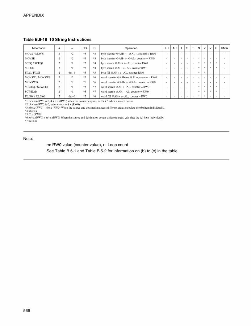
APPENDIX
Note:
m: RW0 value (counter value), n: Loop count
See Table B.5-1 and Table B.5-2 for information on (b) to (c) in the table.
Table B.8-18 10 String Instructions
Mnemonic # ~ RG B Operation LH AH I S T N Z V C RMW
MOVS / MOVSI 2 *2 *5 *3 byte transfer @AH+ ← @AL+, counter = RW0 - - - - - - - - - -
MOVSD 2 *2 *5 *3 byte transfer @AH- ← @AL-, counter = RW0 - - - - - - - - - -
SCEQ / SCEQI 2 *1 *5 *4 byte search @AH+ ← AL, counter RW0 - - - - - * * * * -
SCEQD 2 *1 *5 *4 byte search @AH- ← AL, counter RW0 - - - - - * * * * -
FILS / FILSI 2 6m+6 *5 *3 byte fill @AH+ ← AL, counter RW0 - - - - - * * - - -
MOVSW / MOVSWI 2 *2 *5 *6 word transfer @AH+ ← @AL+, counter = RW0 - - - - - - - - - -
MOVSWD 2 *2 *5 *6 word transfer @AH- ← @AL-, counter = RW0 - - - - - - - - - -
SCWEQ / SCWEQI 2 *1 *5 *7 word search @AH+ - AL, counter = RW0 - - - - - * * * * -
SCWEQD 2 *1 *5 *7 word search @AH- - AL, counter = RW0 - - - - - * * * * -
FILSW / FILSWI 2 6m+6 *5 *6 word fill @AH+ ← AL, counter = RW0 - - - - - * * - - -
*1: 5 when RW0 is 0, 4 + 7 x (RW0) when the counter expires, or 7n + 5 when a match occurs*2: 5 when RW0 is 0; otherwise, 4 + 8 x (RW0)*3: (b) x (RW0) + (b) x (RW0) When the source and destination access different areas, calculate the (b) item individually.*4: (b) x n*5: 2 x (RW0)*6: (c) x (RW0) + (c) x (RW0) When the source and destination access different areas, calculate the (c) item individually.*7: (c) x n
566

APPENDIX B Instructions
B.9 Instruction Map
Each F2MC-16LX instruction code consists of 1 or 2 bytes. Therefore, the instruction
map consists of multiple pages. Table B.9-2 to Table B.9-21 summarize the F2MC-16LX instruction map.
Structure of Instruction Map
Figure B.9-1 Structure of Instruction Map
An instruction such as the NOP instruction that ends in one byte is completed within the basic page. An
instruction such as the MOVS instruction that requires two bytes recognizes the existence of byte 2 when it
references byte 1, and can check the following one byte by referencing the map for byte 2. Figure B.9-2
shows the correspondence between an actual instruction code and instruction map.
Basic page map : Byte 1
Bit operation instructions
Character string operation
instructions
2-byte instructions
ea instructions × 9 : Byte 2
567

APPENDIX
Figure B.9-2 Correspondence between Actual Instruction Code and Instruction Map
An example of an instruction code is shown in Table B.9-1.
*: The extended page map is a generic name of maps for bit operation instructions, characterstring operation instructions, 2-byte instructions, and ea instructions. Actually, there aremultiple extended page maps for each type of instructions.
Some instructions do not contain byte 2.
Length varies depending on the instruction.
Instruction code
Byte 1 Byte 2 Operand Operand . . .
[Basic page map]
XY
+Z
[Extended page map]*
UV
+W
Table B.9-1 Example of an Instruction Code
Instruction Byte 1(from basic page map)
Byte 2(from extended page map)
NOP 00 +0=00 -
AND A, #8 30 +4=34 -
MOV A, ADB 60 +F=6F 00 +0=00
@RW2+d8, #8rel 70 +0=70 F0 +2=F2
568

APPENDIX B Instructions
Table B.9-2 Basic Page Map
0010
2030
4050
6070
8090
A0
B0
C0
D0
E0
F0
+0
NO
PC
MR
AD
DA
, dir
AD
DA
, #8
MO
VA
, dir
MO
VA
, io
BR
Are
lea
in
stru
ctio
n 1
MO
VA
, Ri
MO
VR
i, A
MO
VR
i, #8
MO
VA
, Ri
MO
VX
A,
@R
Wi+
d8M
OV
A, #
4C
ALL
#4B
Z/B
EQ
rel
+1
INT
9N
CC
SU
BA
, dir
SU
BA
, #8
MO
Vdi
r, A
MO
Vio
, AJM
P@
Aea
in
stru
ctio
n 2
BN
Z/B
NE re
l
+2
AD
DD
CA
SU
BD
CA
AD
DC
AS
UB
CA
MO
VA
, #8
MO
VA
, add
r16
JMP ad
dr16
ea
inst
ruct
ion
3B
C/B
L0re
l
+3
NE
GA
JCT
X@
AC
MP
AC
MP
A, #
8M
OV
X A, #
8M
OV
addr
16, A
JMP
P adde
24ea
in
stru
ctio
n 4
BN
C/B
HS re
l
+4
PC
BE
XT
AN
D CC
R, #
8A
ND
A, #
8M
OV di
r, #
8M
OV
io, #
8C
ALL ad
dr16
ea
inst
ruct
ion
5B
Nre
l
+5
DT
BZ
EX
TO
R CC
R, #
8O
RA
, #8
MO
VX A
, dir
MO
VX
A, i
oC
ALL
Pad
dr24
ea
inst
ruct
ion
6B
Pre
l
+6
AD
BS
WA
PD
IVU
AX
OR
A, #
8M
OV
W A, S
PM
OV
W io, #
16R
ET
Pea
in
stru
ctio
n 7
BV
rel
+7
SP
BA
DD
SP
#8M
ULU
AN
OT
AM
OV
W SP
, AM
OV
XA
, add
r16
RE
Tea
in
stru
ctio
n 8
BN
Vre
l
+8
LIN
K #im
m8
AD
DL A
, #32
AD
DW
AA
DD
W A, #
16M
OV
W A, d
irM
OV
WA
, io
INT
#vct
8ea
in
stru
ctio
n 9
MO
VW A, R
Wi
MO
VW RW
i, A
MO
VW
RW
i, #1
6M
OV
A,
@R
Wi+
d8M
OV
W @
RW
i+d8
, AB
Tre
l
+9
UN
LIN
KS
UB
L A, #
32S
UB
WA
SU
BW A
, #16
MO
VW di
r, A
MO
VW
io, A
INT
addr
16M
OV
EA
RW
i, ea
BN
Tre
l
+A
MO
V RP
, #8
MO
V ILM
, #8
CB
NE
A,
#8, r
elC
WB
NE
A,
#16,
rel
MO
VW A, #
16M
OV
WA
,add
r16
INT
P addr
24M
OV
Ri,
eaB
LTre
l
+B
NE
GW
AC
MP
L A, #
32C
MP
WA
CM
PW A, #
16M
OV
L A, #
32M
OV
Wad
dr16
, AR
ET
IM
OV
WR
Wi,
eaB
GE
rel
+C
LSLW
AE
XT
WA
ND
WA
AN
DW A
, #16
PU
SH
WA
PO
PW
AB
it op
erat
ion
inst
ruct
ion
MO
Vea
, Ri
BLE
rel
+D
ZE
XT
WO
RW
AO
RW A
, #16
PU
SH
WA
HP
OP
WA
HM
OV
Wea
, RW
iB
GT
rel
+E
AS
RW
AS
WA
PW
XO
RW
AX
OR
W A, #
16P
US
HW
PS
PO
PW
PS
Cha
ract
er
strin
g op
erat
ion
inst
ruct
ion
XC
HR
i, ea
BLS
rel
+F
LSR
WA
AD
DS
P #16
MU
LUW
AN
OT
WA
PU
SH
Wrls
tP
OP
Wrls
t2-
byte
in
stru
ctio
nX
CH
WR
Wi,
eaB
HI
rel
569

APPENDIX
Table B.9-3 Bit Operation Instruction Map (First Byte = 6CH)
0010
2030
4050
6070
8090
A0
B0
C0
D0
E0
F0
+0
MO
VB
A, i
o:bp
MO
VB
io:b
p, A
CLR
Bio
:bp
SE
TB
io:b
pB
BC io
;bp,
rel
BB
S io:b
p, r
elW
BT
S io:b
pW
BT
C io:b
p
+1
+2
+3
+4
+5
+6
+7
+8
MO
VB
A, d
ir:bp
MO
VB
A,
addr
16:b
pM
OV
Bdi
r:bp
, AM
OV
Bad
dr16
:bp,
AC
LRB di
r:bp
CLR
Bad
dr16
:bp
SE
TB di
r:bp
SE
TB
addr
16:b
pB
BC dir:
bp, r
elB
BC
addr
16:b
p,re
lB
BS dir:
bp, r
elB
BS
addr
16:b
p,re
lS
BB
Sad
dr16
:bp
+9
+A
+B
+C
+D +E +F
570

APPENDIX B Instructions
Table B.9-4 Character String Operation Instruction Map (First Byte = 6EH)
0010
2030
4050
6070
8090
A0
B0
C0
D0
E0
F0
+0
MO
VS
IP
CB
, PC
BM
OV
SD
MO
VS
WI
MO
VS
WD
SC
EQ
I PC
BS
CE
QD P
CB
SC
WE
QI
PC
BS
CW
EQ
DP
CB
FIL
SI
PC
BF
ILS
IP
CB
+1
PC
B, D
TB
DT
BD
TB
DT
BD
TB
DT
BD
TB
+2
PC
B, A
DB
AD
BA
DB
AD
BA
DB
AD
BA
DB
+3
PC
B, S
PB
SP
BS
PB
SP
BS
PB
SP
BS
PB
+4
DT
B, P
CB
+5
DT
B, D
TB
+6
DT
B, A
DB
+7
DT
B, S
PB
+8
AD
B, P
CB
+9
AD
B, D
TB
+A
AD
B, A
DB
+B
AD
B, S
PB
+C
SP
B, P
CB
+D
SP
B, D
TB
+E
SP
B, A
DB
+F
SP
B, S
PB
571

APPENDIX
Table B.9-5 2-byte Instruction Map (First Byte = 6FH)
0010
2030
4050
6070
8090
A0
B0
C0
D0
E0
F0
+0
MO
V A, D
TB
MO
V DT
B, A
MO
VX
A, @
RL0
+d8
MO
V@
RL0
+d8,
AM
OV
A, @
RL0
+d8
+1
MO
V A, A
DB
MO
V AD
B, A
+2
MO
V A, S
SB
MO
V SS
B, A
MO
VX
A, @
RL1
+d8
MO
V@
RL1
+d8,
AM
OV
A, @
RL1
+d8
+3
MO
V A, U
SB
MO
V US
B, A
+4
MO
V A, D
PR
MO
V DP
R, A
MO
VX
A, @
RL2
+d8
MO
V@
RL2
+d8,
AM
OV
A, @
RL2
+d8
+5
MO
V A, @
AM
OV
@A
L, A
H
+6
MO
V A, P
CB
MO
V A, @
AM
OV
XA,
@R
L3+d
8M
OV
@R
L3+d
8, A
MO
VA
, @R
L3+d
8
+7
RO
LCA
RO
LCA
+8
MO
VW
@R
L0+d
8, A
MO
VW
A, @
RL0
+d8
MU
LA
+9
MU
LWA
+A
MO
VW
@R
L1+d
8, A
MO
VW
A, @
RL1
+d8
DIV
UA
+B
+C
LSLW
A, R
0LS
LLA
, R0
LSL
A, R
0M
OV
W@
RL2
+d8,
AM
OV
WA
, @R
L2+d
8
+D
MO
VW A, @
AM
OV
W@
AL,
AH
NR
ML A
, R0
+E
AS
RW A
, R0
AS
RL A
, R0
AS
RA
, R0
MO
VW
@R
L3+d
8, A
MO
VW
A, @
RL3
+d8
+F
LSR
W A, R
0LS
RL A
, R0
LSR
A, R
0
572

APPENDIX B Instructions
Table B.9-6 ea Instruction 1 (First Byte = 70H)
0010
2030
4050
6070
8090
A0
B0
C0
D0
E0
F0
CW
BN
E ↓
CW
BN
E ↓
CB
NE
↓C
BN
E ↓
+0
AD
DL A, R
L0A
DD
L A
,@
RW
0+d8
SU
BL A, R
L0S
UB
L A
,@
RW
0+d8
RW
0,#1
6, r
el@
RW
0+d8
#16,
rel
CM
PL A, R
L0C
MP
L A
,@
RW
0+d8
AN
DL A, R
L0A
ND
L A
,@
RW
0+d8
OR
L A, R
L0O
RL
A,
@R
W0+
d8X
OR
L A, R
L0X
OR
L A
,@
RW
0+d8
R0,
#8, r
el@
RW
0+d8
,#8
, rel
+1
AD
DL A, R
L0A
DD
L A
,@
RW
1+d8
SU
BL A, R
L0S
UB
L A
,@
RW
1+d8
RW
1,#1
6, r
el@
RW
1+d8
#16,
rel
CM
PL A, R
L0C
MP
L A
,@
RW
1+d8
AN
DL A, R
L0A
ND
L A
,@
RW
1+d8
OR
L A, R
L0O
RL
A,
@R
W1+
d8X
OR
L A, R
L0X
OR
L A
,@
RW
1+d8
R1,
#8, r
el@
RW
1+d8
,#8
, rel
+2
AD
DL A, R
L1A
DD
L A
,@
RW
2+d8
SU
BL A, R
L1S
UB
L A
,@
RW
2+d8
RW
2,#1
6, r
el@
RW
2+d8
#16,
rel
CM
PL A, R
L1C
MP
L A
,@
RW
2+d8
AN
DL A, R
L1A
ND
L A
,@
RW
2+d8
OR
L A, R
L1O
RL
A,
@R
W2+
d8X
OR
L A, R
L1X
OR
L A
,@
RW
2+d8
R2,
#8, r
el@
RW
2+d8
,#8
, rel
+3
AD
DL A, R
L1A
DD
L A
,@
RW
3+d8
SU
BL A, R
L1S
UB
L A
,@
RW
3+d8
RW
3,#1
6, r
el@
RW
3+d8
#16,
rel
CM
PL A, R
L1C
MP
L A
,@
RW
3+d8
AN
DL A, R
L1A
ND
L A
,@
RW
3+d8
OR
L A, R
L1O
RL
A,
@R
W3+
d8X
OR
L A, R
L1X
OR
L A
,@
RW
3+d8
R3,
#8, r
el@
RW
3+d8
,#8
, rel
+4
AD
DL A, R
L2A
DD
L A
,@
RW
4+d8
SU
BL A, R
L2S
UB
L A
,@
RW
4+d8
RW
4,#1
6, r
el@
RW
4+d8
#16,
rel
CM
PL A, R
L2C
MP
L A
,@
RW
4+d8
AN
DL A, R
L2A
ND
L A
,@
RW
4+d8
OR
L A, R
L2O
RL
A,
@R
W4+
d8X
OR
L A, R
L2X
OR
L A
,@
RW
4+d8
R4,
#8, r
el@
RW
4+d8
,#8
, rel
+5
AD
DL A, R
L2A
DD
L A
,@
RW
5+d8
SU
BL A, R
L2S
UB
L A
,@
RW
5+d8
RW
5,#1
6, r
el@
RW
5+d8
#16,
rel
CM
PL A, R
L2C
MP
L A
,@
RW
5+d8
AN
DL A, R
L2A
ND
L A
,@
RW
5+d8
OR
L A, R
L2O
RL
A,
@R
W5+
d8X
OR
L A, R
L2X
OR
L A
,@
RW
5+d8
R5,
#8, r
el@
RW
5+d8
,#8
, rel
+6
AD
DL A, R
L3A
DD
L A
,@
RW
6+d8
SU
BL A, R
L3S
UB
L A
,@
RW
6+d8
RW
6,#1
6, r
el@
RW
6+d8
#16,
rel
CM
PL A, R
L3C
MP
L A
,@
RW
6+d8
AN
DL A, R
L3A
ND
L A
,@
RW
6+d8
OR
L A, R
L3O
RL
A,
@R
W6+
d8X
OR
L A, R
L3X
OR
L A
,@
RW
6+d8
R6,
#8, r
el@
RW
6+d8
,#8
, rel
+7
AD
DL A, R
L3A
DD
L A
,@
RW
7+d8
SU
BL A, R
L3S
UB
L A
,@
RW
7+d8
RW
7,#1
6, r
el@
RW
7+d8
#16,
rel
CM
PL A, R
L3C
MP
L A
,@
RW
7+d8
AN
DL A, R
L3A
ND
L A
,@
RW
7+d8
OR
L A, R
L3O
RL
A,
@R
W7+
d8X
OR
L A, R
L3X
OR
L A
,@
RW
7+d8
R7,
#8, r
el@
RW
7+d8
,#8
, rel
+8
AD
DL
A,@
RW
0A
DD
L A
,@
RW
0+d1
6S
UB
LA
,@R
W0
SU
BL
A,
@R
W0+
d16
@R
W0,
#16,
rel
@R
W0+
d16
#16,
rel
CM
PL
A,@
RW
0C
MP
L A
,@
RW
0+d1
6A
ND
LA
,@R
W0
AN
DL
A,
@R
W0+
d16
OR
LA
,@R
W0
OR
L A
,@
RW
0+d1
6X
OR
LA
,@R
W0
XO
RL
A,
@R
W0+
d16
@R
W0,
#8, r
el@
RW
0+d1
6,#
8, r
el
+9
AD
DL
A,@
RW
1A
DD
L A
,@
RW
1+d1
6S
UB
LA
,@R
W1
SU
BL
A,
@R
W1+
d16
@R
W1,
#16,
rel
@R
W1+
d16
#16,
rel
CM
PL
A,@
RW
1C
MP
L A
,@
RW
1+d1
6A
ND
LA
,@R
W1
AN
DL
A,
@R
W1+
d16
OR
LA
,@R
W1
OR
L A
,@
RW
1+d1
6X
OR
LA
,@R
W1
XO
RL
A,
@R
W1+
d16
@R
W1,
#8, r
el@
RW
1+d1
6,#
8, r
el
+A
AD
DL
A,@
RW
2A
DD
L A
,@
RW
2+d1
6S
UB
LA
,@R
W2
SU
BL
A,
@R
W2+
d16
@R
W2,
#16,
rel
@R
W2+
d16
#16,
rel
CM
PL
A,@
RW
2C
MP
L A
,@
RW
2+d1
6A
ND
LA
,@R
W2
AN
DL
A,
@R
W2+
d16
OR
LA
,@R
W2
OR
L A
,@
RW
2+d1
6X
OR
LA
,@R
W2
XO
RL
A,
@R
W2+
d16
@R
W2,
#8, r
el@
RW
2+d1
6,#
8, r
el
+B
AD
DL
A,@
RW
3A
DD
L A
,@
RW
3+d1
6S
UB
LA
,@R
W3
SU
BL
A,
@R
W3+
d16
@R
W3,
#16,
rel
@R
W3+
d16
#16,
rel
CM
PL
A,@
RW
3C
MP
L A
,@
RW
3+d1
6A
ND
LA
,@R
W3
AN
DL
A,
@R
W3+
d16
OR
LA
,@R
W3
OR
L A
,@
RW
3+d1
6X
OR
LA
,@R
W3
XO
RL
A,
@R
W3+
d16
@R
W3,
#8, r
el@
RW
3+d1
6,#
8, r
el
+C
AD
DL
A,@
RW
0+A
DD
L A
,@
RW
0+R
W7
SU
BL
A,@
RW
0+S
UB
L A
,@
RW0+
RW
7U
se
proh
ibite
d@
RW0+
RW
7#1
6, r
elC
MP
LA
,@R
W0+
CM
PL
A,
@R
W0+
RW7
AN
DL
A,@
RW
0+A
ND
L A
,@
RW
0+R
W7
OR
LA
,@R
W0+
OR
L A
,@
RW
0+RW
7X
OR
LA
,@R
W0+
XO
RL
A,
@R
W0+
RW
7U
se
proh
ibite
d@
RW0+
RW
7,#
8, r
el
+D
AD
DL
A,@
RW
1+A
DD
L A
,@
RW
1+R
W7
SU
BL
A,@
RW
1+S
UB
L A
,@
RW1+
RW
7U
se
proh
ibite
d@
RW1+
RW
7#1
6, r
elC
MP
LA
,@R
W1+
CM
PL
A,
@R
W1+
RW7
AN
DL
A,@
RW
1+A
ND
L A
,@
RW
1+R
W7
OR
LA
,@R
W1+
OR
L A
,@
RW
1+RW
7X
OR
LA
,@R
W1+
XO
RL
A,
@R
W1+
RW
7U
se
proh
ibite
d@
RW1+
RW
7,#
8, r
el
+E
AD
DL
A,@
RW
2+A
DD
L A
,@
PC
+d16
SU
BL
A,@
RW
2+S
UB
L A
,@
PC
+d16
Use
pr
ohib
ited
@P
C+d
16,
#16,
rel
CM
PL
A,@
RW
2+C
MP
L A
,@
PC
+d16
AN
DL
A,@
RW
2+A
ND
L A
,@
PC
+d16
OR
LA
,@R
W2+
OR
L A
,@
PC
+d16
XO
RL
A,@
RW
2+X
OR
L A
,@
PC
+d16
Use
pr
ohib
ited
@P
C+d
16,
,#8,
rel
+F
AD
DL
A,@
RW
3+A
DD
L A
,ad
dr16
SU
BL
A,@
RW
3+S
UB
L A
,ad
dr16
Use
pr
ohib
ited
addr
16,
#16,
rel
CM
PL
A,@
RW
3+C
MP
L A
,ad
dr16
AN
DL
A,@
RW
3+A
ND
L A
,ad
dr16
OR
LA
,@R
W3+
OR
L A
,ad
dr16
XO
RL
A,@
RW
3+X
OR
L A
,ad
dr16
Use
pr
ohib
ited
addr
16,
,#8,
rel
573

APPENDIX
Table B.9-7 ea Instruction 2 (First Byte = 71H)
0010
2030
4050
6070
8090
A0
B0
C0
D0
E0
F0
+0
JMP
P @R
L0JM
PP@
@R
W0+
d8C
ALL
P@
RL0
CAL
LP@
@R
W0+
d8IN
CL
RL0
INC
L@
RW
0+d8
DE
CL
RL0
DE
CL
@R
W0+
d8M
OV
LA
, RL0
MO
VL
A,
@R
W0+
d8M
OV
LR
L0, A
MO
VL
@R
W0+
d8,A
MO
V R0,
#8
MO
V@
RW
0+d8
,#8
MO
VE
AA
, RW
0M
OV
EA
A,
@R
W0+
d8
+1
JMP
P @R
L0JM
PP@
@R
W1+
d8C
ALL
P@
RL0
CAL
LP@
@R
W1+
d8IN
CL
RL0
INC
L@
RW
1+d8
DE
CL
RL0
DE
CL
@R
W1+
d8M
OV
LA
, RL0
MO
VL
A,
@R
W1+
d8M
OV
LR
L0, A
MO
VL
@R
W1+
d8,A
MO
V R1,
#8
MO
V@
RW
1+d8
,#8
MO
VE
AA
, RW
1M
OV
EA
A,
@R
W1+
d8
+2
JMP
P @R
L1JM
PP@
@R
W2+
d8C
ALL
P@
RL1
CAL
LP@
@R
W2+
d8IN
CL
RL1
INC
L@
RW
2+d8
DE
CL
RL1
DE
CL
@R
W2+
d8M
OV
LA
, RL1
MO
VL
A,
@R
W2+
d8M
OV
LR
L1, A
MO
VL
@R
W2+
d8,A
MO
V R2,
#8
MO
V@
RW
2+d8
,#8
MO
VE
AA
, RW
2M
OV
EA
A,
@R
W2+
d8
+3
JMP
P @R
L1JM
PP@
@R
W3+
d8C
ALL
P@
RL1
CAL
LP@
@R
W3+
d8IN
CL
RL1
INC
L@
RW
3+d8
DE
CL
RL1
DE
CL
@R
W3+
d8M
OV
LA
, RL1
MO
VL
A,
@R
W3+
d8M
OV
LR
L1, A
MO
VL
@R
W3+
d8,A
MO
V R3,
#8
MO
V@
RW
3+d8
,#8
MO
VE
AA
, RW
3M
OV
EA
A,
@R
W3+
d8
+4
JMP
P @R
L2JM
PP@
@R
W4+
d8C
ALL
P@
RL2
CAL
LP@
@R
W4+
d8IN
CL
RL2
INC
L@
RW
4+d8
DE
CL
RL2
DE
CL
@R
W4+
d8M
OV
LA
, RL2
MO
VL
A,
@R
W4+
d8M
OV
LR
L2, A
MO
VL
@R
W4+
d8,A
MO
V R4,
#8
MO
V@
RW
4+d8
,#8
MO
VE
AA
, RW
4M
OV
EA
A,
@R
W4+
d8
+5
JMP
P @R
L2JM
PP@
@R
W5+
d8C
ALL
P@
RL2
CAL
LP@
@R
W5+
d8IN
CL
RL2
INC
L@
RW
5+d8
DE
CL
RL2
DE
CL
@R
W5+
d8M
OV
LA
, RL2
MO
VL
A,
@R
W5+
d8M
OV
LR
L2, A
MO
VL
@R
W5+
d8,A
MO
V R5,
#8
MO
V@
RW
5+d8
,#8
MO
VE
AA
, RW
5M
OV
EA
A,
@R
W5+
d8
+6
JMP
P @R
L3JM
PP@
@R
W6+
d8C
ALL
P@
RL3
CAL
LP@
@R
W6+
d8IN
CL
RL3
INC
L@
RW
6+d8
DE
CL
RL3
DE
CL
@R
W6+
d8M
OV
LA
, RL3
MO
VL
A,
@R
W6+
d8M
OV
LR
L3, A
MO
VL
@R
W6+
d8,A
MO
V R6,
#8
MO
V@
RW
6+d8
,#8
MO
VE
AA
, RW
6M
OV
EA
A,
@R
W6+
d8
+7
JMP
P @R
L3JM
PP@
@R
W7+
d8C
ALL
P@
RL3
CAL
LP@
@R
W7+
d8IN
CL
RL3
INC
L@
RW
7+d8
DE
CL
RL3
DE
CL
@R
W7+
d8M
OV
LA
, RL3
MO
VL
A,
@R
W7+
d8M
OV
LR
L3, A
MO
VL
@R
W7+
d8,A
MO
V R7,
#8
MO
V@
RW
7+d8
,#8
MO
VE
AA
, RW
7M
OV
EA
A,
@R
W7+
d8
+8
JMP
P@
@R
W0
JMP
P @
@R
W0+
d16
CA
LLP
@@
RW
0C
ALL
P @
@R
W0+
d16
INC
L @R
W0
INC
L@
RW
0+d1
6D
EC
L@
RW
0D
EC
L@
RW
0+d1
6M
OV
LA
,@R
W0
MO
VL
A,
@R
W0+
d16
MO
VL
@R
W0,
AM
OVL
@R
W0+
d16,
AM
OV
@R
W0,
#8
MO
V@
RW0+
d16,
#8M
OV
EA
A,@
RW
0M
OV
EA
A,
@R
W0+
d16
+9
JMP
P@
@R
W1
JMP
P @
@R
W1+
d16
CA
LLP
@@
RW
1C
ALL
P @
@R
W1+
d16
INC
L @R
W1
INC
L@
RW
1+d1
6D
EC
L@
RW
1D
EC
L@
RW
1+d1
6M
OV
LA
,@R
W1
MO
VL
A,
@R
W1+
d16
MO
VL
@R
W1,
AM
OVL
@R
W1+
d16,
AM
OV
@R
W1,
#8
MO
V@
RW1+
d16,
#8M
OV
EA
A,@
RW
1M
OV
EA
A,
@R
W1+
d16
+A
JMP
P@
@R
W2
JMP
P @
@R
W2+
d16
CA
LLP
@@
RW
2C
ALL
P @
@R
W2+
d16
INC
L @R
W2
INC
L@
RW
2+d1
6D
EC
L@
RW
2D
EC
L@
RW
2+d1
6M
OV
LA
,@R
W2
MO
VL
A,
@R
W2+
d16
MO
VL
@R
W2,
AM
OVL
@R
W2+
d16,
AM
OV
@R
W2,
#8
MO
V@
RW2+
d16,
#8M
OV
EA
A,@
RW
2M
OV
EA
A,
@R
W2+
d16
+B
JMP
P@
@R
W3
JMP
P @
@R
W3+
d16
CA
LLP
@@
RW
3C
ALL
P @
@R
W3+
d16
INC
L @R
W3
INC
L@
RW
3+d1
6D
EC
L@
RW
3D
EC
L@
RW
3+d1
6M
OV
LA
,@R
W3
MO
VL
A,
@R
W3+
d16
MO
VL
@R
W3,
AM
OVL
@R
W3+
d16,
AM
OV
@R
W3,
#8
MO
V@
RW3+
d16,
#8M
OV
EA
A,@
RW
3M
OV
EA
A,
@R
W3+
d16
+C
JMP
P@
@R
W0+
JMPP
@@
RW
0+RW
7C
ALL
P@
@R
W0+
CAL
LP @
@R
W0+
RW7
INC
L@
RW
0+IN
CL@
RW0+
RW7
DE
CL
@R
W0+
DECL
@R
W0+
RW7
MO
VL
A,@
RW
0+M
OVL
A,
@R
W0+
RW7
MO
VL
@R
W0+
,AM
OVL
@RW
0+RW
7,A
MO
V@
RW
0+, #
8M
OV
@RW
0+RW
7,#8
MO
VE
AA
,@R
W0+
MO
VEA
A,@
RW
0+RW
7
+D
JMP
P@
@R
W1+
JMPP
@@
RW
1+RW
7C
ALL
P@
@R
W1+
CAL
LP @
@R
W1+
RW7
INC
L@
RW
1+IN
CL@
RW1+
RW7
DE
CL
@R
W1+
DECL
@R
W1+
RW7
MO
VL
A,@
RW
1+M
OVL
A,
@R
W1+
RW7
MO
VL
@R
W1+
,AM
OVL
@RW
1+RW
7,A
MO
V@
RW
1+, #
8M
OV
@RW
1+RW
7,#8
MO
VE
AA
,@R
W1+
MO
VEA
A,@
RW
1+RW
7
+E
JMP
P@
@R
W2+
JMPP
@@
PC+d
16C
ALL
P@
@R
W2+
CAL
LP@
@PC
+d16
INC
L@
RW
2+IN
CL
@P
C+
d16
DE
CL
@R
W2+
DE
CL
@P
C+
d16
MO
VL
A,@
RW
2+M
OV
L A
,@
PC
+d1
6M
OV
L@
RW
2+,A
MO
VL
@P
C+d
16, A
MO
V@
RW
2+, #
8M
OV
@P
C+d
16, #
8M
OV
EA
A,@
RW
2+M
OV
EA
A,
@P
C+
d16
+F
JMP
P@
@R
W3+
JMP
P@
addr
16C
ALL
P@
@R
W3+
CA
LLP
@ad
dr16
INC
L@
RW
3+IN
CL ad
dr16
DE
CL
@R
W3+
DE
CL ad
dr16
MO
VL
A,@
RW
3+M
OV
L A
,ad
dr16
MO
VL
@R
W3+
,AM
OV
Lad
dr16
, AM
OV
@R
W3+
, #8
MO
V addr
16, #
8M
OV
EA
A,@
RW
3+M
OV
EA
A,
addr
16
574

APPENDIX B Instructions
Table B.9-8 ea Instruction 3 (First Byte = 72H)
0010
2030
4050
6070
8090
A0
B0
C0
D0
E0
F0
+0
RO
LCR
0R
OLC
@R
W0+
d8R
OR
CR
0R
OR
C@
RW
0+d8
INC
R0
INC
@R
W0+
d8D
EC
R0
DE
C@
RW
0+d8
MO
VA
, R0
MO
V
A
,@
RW
0+d8
MO
VR
0, A
MO
V@
RW
0+d8
,AM
OV
X A, R
0M
OV
X
A,
@R
W0+
d8X
CH
A, R
0X
CH
A,
@R
W0+
d8
+1
RO
LCR
1R
OLC
@R
W1+
d8R
OR
CR
1R
OR
C@
RW
1+d8
INC
R1
INC
@R
W1+
d8D
EC
R1
DE
C@
RW
1+d8
MO
VA
, R1
MO
V
A
,@
RW
1+d8
MO
VR
1, A
MO
V@
RW
1+d8
,AM
OV
X A, R
1M
OV
X
A,
@R
W1+
d8X
CH
A, R
1X
CH
A,
@R
W1+
d8
+2
RO
LCR
2R
OLC
@R
W2+
d8R
OR
CR
2R
OR
C@
RW
2+d8
INC
R2
INC
@R
W2+
d8D
EC
R2
DE
C@
RW
2+d8
MO
VA
, R2
MO
V
A
,@
RW
2+d8
MO
VR
2, A
MO
V@
RW
2+d8
,AM
OV
X A, R
2M
OV
X
A,
@R
W2+
d8X
CH
A, R
2X
CH
A,
@R
W2+
d8
+3
RO
LCR
3R
OLC
@R
W3+
d8R
OR
CR
3R
OR
C@
RW
3+d8
INC
R3
INC
@R
W3+
d8D
EC
R3
DE
C@
RW
3+d8
MO
VA
, R3
MO
V
A
,@
RW
3+d8
MO
VR
3, A
MO
V@
RW
3+d8
,AM
OV
X A, R
3M
OV
X
A,
@R
W3+
d8X
CH
A, R
3X
CH
A,
@R
W3+
d8
+4
RO
LCR
4R
OLC
@R
W4+
d8R
OR
CR
4R
OR
C@
RW
4+d8
INC
R4
INC
@R
W4+
d8D
EC
R4
DE
C@
RW
4+d8
MO
VA
, R4
MO
V
A
,@
RW
4+d8
MO
VR
4, A
MO
V@
RW
4+d8
,AM
OV
X A, R
4M
OV
X
A,
@R
W4+
d8X
CH
A, R
4X
CH
A,
@R
W4+
d8
+5
RO
LCR
5R
OLC
@R
W5+
d8R
OR
CR
5R
OR
C@
RW
5+d8
INC
R5
INC
@R
W5+
d8D
EC
R5
DE
C@
RW
5+d8
MO
VA
, R5
MO
V
A
,@
RW
5+d8
MO
VR
5, A
MO
V@
RW
5+d8
,AM
OV
X A, R
5M
OV
X
A,
@R
W5+
d8X
CH
A, R
5X
CH
A,
@R
W5+
d8
+6
RO
LCR
6R
OLC
@R
W6+
d8R
OR
CR
6R
OR
C@
RW
6+d8
INC
R6
INC
@R
W6+
d8D
EC
R6
DE
C@
RW
6+d8
MO
VA
, R6
MO
V
A
,@
RW
6+d8
MO
VR
6, A
MO
V@
RW
6+d8
,AM
OV
X A, R
6M
OV
X
A,
@R
W6+
d8X
CH
A, R
6X
CH
A,
@R
W6+
d8
+7
RO
LCR
7R
OLC
@R
W7+
d8R
OR
CR
7R
OR
C@
RW
7+d8
INC
R7
INC
@R
W7+
d8D
EC
R7
DE
C@
RW
7+d8
MO
VA
, R7
MO
V
A
,@
RW
7+d8
MO
VR
7, A
MO
V@
RW
7+d8
,AM
OV
X A, R
7M
OV
X
A,
@R
W7+
d8X
CH
A, R
7X
CH
A,
@R
W7+
d8
+8
RO
LC @R
W0
RO
LC@
RW
0+d1
6R
OR
C@
RW
0R
OR
C@
RW
0+d1
6IN
C @R
W0
INC
@R
W0+
d16
DE
C @R
W0
DE
C@
RW
0+d1
6M
OV
A,@
RW
0M
OV
A,
@R
W0+
d16
MO
V@
RW
0, A
MO
V@
RW
0+d1
6,A
MO
VX
A,@
RW
0M
OV
X
A,
@R
W0+
d16
XC
HA
,@R
W0
XC
H
A
,@
RW
0+d1
6
+9
RO
LC @R
W1
RO
LC@
RW
1+d1
6R
OR
C@
RW
1R
OR
C@
RW
1+d1
6IN
C @R
W1
INC
@R
W1+
d16
DE
C @R
W1
DE
C@
RW
1+d1
6M
OV
A,@
RW
1M
OV
A,
@R
W1+
d16
MO
V@
RW
1, A
MO
V@
RW
1+d1
6,A
MO
VX
A,@
RW
1M
OV
X
A,
@R
W1+
d16
XC
HA
,@R
W1
XC
H
A
,@
RW
1+d1
6
+A
RO
LC @R
W2
RO
LC@
RW
2+d1
6R
OR
C@
RW
2R
OR
C@
RW
2+d1
6IN
C @R
W2
INC
@R
W2+
d16
DE
C @R
W2
DE
C@
RW
2+d1
6M
OV
A,@
RW
2M
OV
A,
@R
W2+
d16
MO
V@
RW
2, A
MO
V@
RW
2+d1
6,A
MO
VX
A,@
RW
2M
OV
X
A,
@R
W2+
d16
XC
HA
,@R
W2
XC
H
A
,@
RW
2+d1
6
+B
RO
LC @R
W3
RO
LC@
RW
3+d1
6R
OR
C@
RW
3R
OR
C@
RW
3+d1
6IN
C @R
W3
INC
@R
W3+
d16
DE
C @R
W3
DE
C@
RW
3+d1
6M
OV
A,@
RW
3M
OV
A,
@R
W3+
d16
MO
V@
RW
3, A
MO
V@
RW
3+d1
6,A
MO
VX
A,@
RW
3M
OV
X
A,
@R
W3+
d16
XC
HA
,@R
W3
XC
H
A
,@
RW
3+d1
6
+C
RO
LC@
RW
0+R
OLC
@R
W0+
RW7
RO
RC
@R
W0+
RORC
@R
W0+
RW7
INC @
RW
0+IN
C@
RW
0+RW
7D
EC @R
W0+
DEC
@R
W0+
RW7
MO
VA
,@R
W0+
MO
V
A,
@R
W0+
RW7
MO
V@
RW
0+, A
MOV
@RW
0+RW
7,A
MO
VX
A,@
RW
0+M
OVX
A,
@RW
0+RW
7X
CH
A,@
RW
0+XC
H
A,
@RW
0+RW
7
+D
RO
LC@
RW
1+R
OLC
@R
W1+
RW7
RO
RC
@R
W1+
RORC
@R
W1+
RW7
INC @
RW
1+IN
C@
RW
1+RW
7D
EC @R
W1+
DEC
@R
W1+
RW7
MO
VA
,@R
W1+
MO
V
A,
@R
W1+
RW7
MO
V@
RW
1+, A
MOV
@RW
1+RW
7,A
MO
VX
A,@
RW
1+M
OVX
A,
@RW
1+RW
7X
CH
A,@
RW
1+XC
H
A,
@RW
1+RW
7
+E
RO
LC@
RW
2+R
OLC
@P
C+
d16
RO
RC
@R
W2+
RO
RC
@P
C+
d16
INC @
RW
2+IN
C@
PC
+d1
6D
EC @R
W2+
DE
C@
PC
+d1
6M
OV
A,@
RW
2+M
OV
A,
@P
C+
d16
MO
V@
RW
2+, A
MO
V@
PC
+d16
, AM
OV
XA
,@R
W2+
MO
VX
A
,@
PC
+d1
6X
CH
A,@
RW
2+X
CH
A,
@P
C+
d16
+F
RO
LC@
RW
3+R
OLC ad
dr16
RO
RC
@R
W3+
RO
RC ad
dr16
INC @
RW
3+IN
Cad
dr16
DE
C @R
W3+
DE
C addr
16M
OV
A,@
RW
3+M
OV
A,
addr
16M
OV
@R
W3+
, AM
OV addr
16, A
MO
VX
A,@
RW
3+M
OV
X
A,
addr
16X
CH
A,@
RW
3+X
CH
A,
addr
16
575
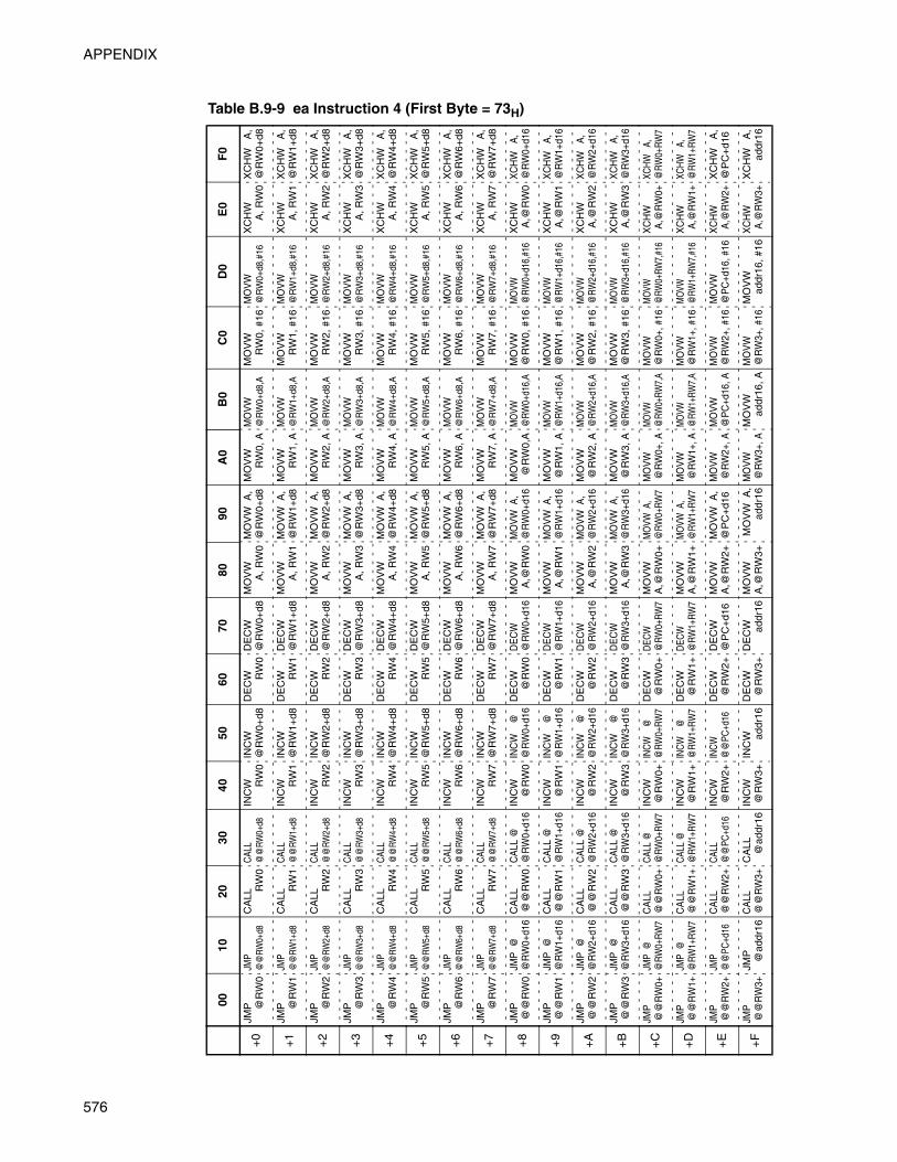
APPENDIX
Table B.9-9 ea Instruction 4 (First Byte = 73H)
0010
2030
4050
6070
8090
A0
B0
C0
D0
E0
F0
+0
JMP @
RW
0JM
P@
@RW
0+d8
CA
LLR
W0
CAL
L@
@RW
0+d8
INC
W RW
0IN
CW
@R
W0+
d8D
EC
W RW
0D
EC
W@
RW
0+d8
MO
VW
A, R
W0
MO
VW
A,
@R
W0+
d8M
OV
WR
W0,
AM
OV
W@
RW
0+d8
,AM
OV
WR
W0,
#16
MO
VW
@R
W0+
d8,#
16X
CH
WA
, RW
0X
CH
W
A,
@R
W0+
d8
+1
JMP @
RW
1JM
P@
@RW
1+d8
CA
LLR
W1
CAL
L@
@RW
1+d8
INC
W RW
1IN
CW
@R
W1+
d8D
EC
W RW
1D
EC
W@
RW
1+d8
MO
VW
A, R
W1
MO
VW
A,
@R
W1+
d8M
OV
WR
W1,
AM
OV
W@
RW
1+d8
,AM
OV
WR
W1,
#16
MO
VW
@R
W1+
d8,#
16X
CH
WA
, RW
1X
CH
W
A,
@R
W1+
d8
+2
JMP @
RW
2JM
P@
@RW
2+d8
CA
LLR
W2
CAL
L@
@RW
2+d8
INC
W RW
2IN
CW
@R
W2+
d8D
EC
W RW
2D
EC
W@
RW
2+d8
MO
VW
A, R
W2
MO
VW
A,
@R
W2+
d8M
OV
WR
W2,
AM
OV
W@
RW
2+d8
,AM
OV
WR
W2,
#16
MO
VW
@R
W2+
d8,#
16X
CH
WA
, RW
2X
CH
W
A,
@R
W2+
d8
+3
JMP @
RW
3JM
P@
@RW
3+d8
CA
LLR
W3
CAL
L@
@RW
3+d8
INC
W RW
3IN
CW
@R
W3+
d8D
EC
W RW
3D
EC
W@
RW
3+d8
MO
VW
A, R
W3
MO
VW
A,
@R
W3+
d8M
OV
WR
W3,
AM
OV
W@
RW
3+d8
,AM
OV
WR
W3,
#16
MO
VW
@R
W3+
d8,#
16X
CH
WA
, RW
3X
CH
W
A,
@R
W3+
d8
+4
JMP @
RW
4JM
P@
@RW
4+d8
CA
LLR
W4
CAL
L@
@RW
4+d8
INC
W RW
4IN
CW
@R
W4+
d8D
EC
W RW
4D
EC
W@
RW
4+d8
MO
VW
A, R
W4
MO
VW
A,
@R
W4+
d8M
OV
WR
W4,
AM
OV
W@
RW
4+d8
,AM
OV
WR
W4,
#16
MO
VW
@R
W4+
d8,#
16X
CH
WA
, RW
4X
CH
W
A,
@R
W4+
d8
+5
JMP @
RW
5JM
P@
@RW
5+d8
CA
LLR
W5
CAL
L@
@RW
5+d8
INC
W RW
5IN
CW
@R
W5+
d8D
EC
W RW
5D
EC
W@
RW
5+d8
MO
VW
A, R
W5
MO
VW
A,
@R
W5+
d8M
OV
WR
W5,
AM
OV
W@
RW
5+d8
,AM
OV
WR
W5,
#16
MO
VW
@R
W5+
d8,#
16X
CH
WA
, RW
5X
CH
W
A,
@R
W5+
d8
+6
JMP @
RW
6JM
P@
@RW
6+d8
CA
LLR
W6
CAL
L@
@RW
6+d8
INC
W RW
6IN
CW
@R
W6+
d8D
EC
W RW
6D
EC
W@
RW
6+d8
MO
VW
A, R
W6
MO
VW
A,
@R
W6+
d8M
OV
WR
W6,
AM
OV
W@
RW
6+d8
,AM
OV
WR
W6,
#16
MO
VW
@R
W6+
d8,#
16X
CH
WA
, RW
6X
CH
W
A,
@R
W6+
d8
+7
JMP @
RW
7JM
P@
@RW
7+d8
CA
LLR
W7
CAL
L@
@RW
7+d8
INC
W RW
7IN
CW
@R
W7+
d8D
EC
W RW
7D
EC
W@
RW
7+d8
MO
VW
A, R
W7
MO
VW
A,
@R
W7+
d8M
OV
WR
W7,
AM
OV
W@
RW
7+d8
,AM
OV
WR
W7,
#16
MO
VW
@R
W7+
d8,#
16X
CH
WA
, RW
7X
CH
W
A,
@R
W7+
d8
+8
JMP
@@
RW
0JM
P @
@R
W0+
d16
CA
LL@
@R
W0
CA
LL @
@R
W0+
d16
INC
W@
RW
0IN
CW
@
@R
W0+
d16
DE
CW
@R
W0
DE
CW
@R
W0+
d16
MO
VW
A,@
RW
0M
OV
W A
,@
RW
0+d1
6M
OV
W@
RW
0,A
MO
VW@
RW0+
d16,
AM
OV
W@
RW
0, #
16M
OVW
@R
W0+
d16,
#16
XC
HW
A,@
RW
0X
CH
W
A,
@R
W0+
d16
+9
JMP
@@
RW
1JM
P @
@R
W1+
d16
CA
LL@
@R
W1
CA
LL @
@R
W1+
d16
INC
W@
RW
1IN
CW
@
@R
W1+
d16
DE
CW
@R
W1
DE
CW
@R
W1+
d16
MO
VW
A,@
RW
1M
OV
W A
,@
RW
1+d1
6M
OV
W@
RW
1, A
MO
VW@
RW1+
d16,
AM
OV
W@
RW
1, #
16M
OVW
@R
W1+
d16,
#16
XC
HW
A,@
RW
1X
CH
W
A,
@R
W1+
d16
+A
JMP
@@
RW
2JM
P @
@R
W2+
d16
CA
LL@
@R
W2
CA
LL @
@R
W2+
d16
INC
W@
RW
2IN
CW
@
@R
W2+
d16
DE
CW
@R
W2
DE
CW
@R
W2+
d16
MO
VW
A,@
RW
2M
OV
W A
,@
RW
2+d1
6M
OV
W@
RW
2, A
MO
VW@
RW2+
d16,
AM
OV
W@
RW
2, #
16M
OVW
@R
W2+
d16,
#16
XC
HW
A,@
RW
2X
CH
W
A,
@R
W2+
d16
+B
JMP
@@
RW
3JM
P @
@R
W3+
d16
CA
LL@
@R
W3
CA
LL @
@R
W3+
d16
INC
W@
RW
3IN
CW
@
@R
W3+
d16
DE
CW
@R
W3
DE
CW
@R
W3+
d16
MO
VW
A,@
RW
3M
OV
W A
,@
RW
3+d1
6M
OV
W@
RW
3, A
MO
VW@
RW3+
d16,
AM
OV
W@
RW
3, #
16M
OVW
@R
W3+
d16,
#16
XC
HW
A,@
RW
3X
CH
W
A,
@R
W3+
d16
+C
JMP
@@
RW
0+JM
P @
@RW
0+R
W7
CA
LL@
@R
W0+
CAL
L @
@RW
0+R
W7
INC
W@
RW
0+IN
CW
@
@RW
0+R
W7
DE
CW
@R
W0+
DECW
@R
W0+
RW7
MO
VW
A,@
RW
0+M
OVW
A,
@RW
0+RW
7M
OV
W@
RW
0+, A
MO
VW@
RW0+
RW7,
AM
OV
W@
RW
0+, #
16M
OVW
@RW
0+RW
7,#1
6X
CH
WA
,@R
W0+
XCH
W
A,@
RW
0+RW
7
+D
JMP
@@
RW
1+JM
P @
@RW
1+R
W7
CA
LL@
@R
W1+
CAL
L @
@RW
1+R
W7
INC
W@
RW
1+IN
CW
@
@RW
1+R
W7
DE
CW
@R
W1+
DECW
@R
W1+
RW7
MO
VW
A,@
RW
1+M
OVW
A,
@RW
1+RW
7M
OV
W@
RW
1+, A
MO
VW@
RW1+
RW7,
AM
OV
W@
RW
1+, #
16M
OVW
@RW
1+RW
7,#1
6X
CH
WA
,@R
W1+
XCH
W
A,@
RW
1+RW
7
+E
JMP
@@
RW
2+JM
P@
@PC
+d16
CA
LL@
@R
W2+
CAL
L@
@PC
+d16
INC
W@
RW
2+IN
CW
@@
PC+d
16D
EC
W@
RW
2+D
EC
W@
PC
+d1
6M
OV
WA
,@R
W2+
MO
VW
A,
@P
C+
d16
MO
VW
@R
W2+
, AM
OV
W@
PC
+d16
, AM
OV
W@
RW
2+, #
16M
OV
W@
PC
+d16
, #16
XC
HW
A,@
RW
2+X
CH
W
A,
@P
C+
d16
+F
JMP
@@
RW
3+JM
P @ad
dr16
CA
LL@
@R
W3+
CA
LL @ad
dr16
INC
W@
RW
3+IN
CW ad
dr16
DE
CW
@R
W3+
DE
CW ad
dr16
MO
VW
A,@
RW
3+M
OV
W A
,ad
dr16
MO
VW
@R
W3+
, AM
OV
Wad
dr16
, AM
OV
W@
RW
3+, #
16M
OV
Wad
dr16
, #16
XC
HW
A,@
RW
3+X
CH
W
A,
addr
16
576

APPENDIX B Instructions
Table B.9-10 ea Instruction 5 (First Byte = 74H)
0010
2030
4050
6070
8090
A0
B0
C0
D0
E0
F0
+0
AD
DA
, R0
AD
D
A
,@
RW
0+d8
SU
BA
, R0
SU
B
A
,@
RW
0+d8
AD
DC A
, R0
AD
DC
A
,@
RW
0+d8
CM
PA
, R0
CM
P
A
,@
RW
0+d8
AN
DA
, R0
AN
D
A
,@
RW
0+d8
OR
A, R
0O
R
A,
@R
W0+
d8X
OR
A, R
0X
OR
A,
@R
W0+
d8D
BN
Z R0,
rD
BN
Z
@R
W0+
d8, r
+1
AD
DA
, R1
AD
D
A
,@
RW
1+d8
SU
BA
, R1
SU
B
A
,@
RW
1+d8
AD
DC A
, R1
AD
DC
A
,@
RW
1+d8
CM
PA
, R1
CM
P
A
,@
RW
1+d8
AN
DA
, R1
AN
D
A
,@
RW
1+d8
OR
A, R
1O
R
A,
@R
W1+
d8X
OR
A, R
1X
OR
A,
@R
W1+
d8D
BN
Z R1,
rD
BN
Z
@R
W1+
d8, r
+2
AD
DA
, R2
AD
D
A
,@
RW
2+d8
SU
BA
, R2
SU
B
A
,@
RW
2+d8
AD
DC A
, R2
AD
DC
A
,@
RW
2+d8
CM
PA
, R2
CM
P
A
,@
RW
2+d8
AN
DA
, R2
AN
D
A
,@
RW
2+d8
OR
A, R
2O
R
A,
@R
W2+
d8X
OR
A, R
2X
OR
A,
@R
W2+
d8D
BN
Z R2,
rD
BN
Z
@R
W2+
d8, r
+3
AD
DA
, R3
AD
D
A
,@
RW
3+d8
SU
BA
, R3
SU
B
A
,@
RW
3+d8
AD
DC A
, R3
AD
DC
A
,@
RW
3+d8
CM
PA
, R3
CM
P
A
,@
RW
3+d8
AN
DA
, R3
AN
D
A
,@
RW
3+d8
OR
A, R
3O
R
A,
@R
W3+
d8X
OR
A, R
3X
OR
A,
@R
W3+
d8D
BN
Z R3,
rD
BN
Z
@R
W3+
d8, r
+4
AD
DA
, R4
AD
D
A
,@
RW
4+d8
SU
BA
, R4
SU
B
A
,@
RW
4+d8
AD
DC A
, R4
AD
DC
A
,@
RW
4+d8
CM
PA
, R4
CM
P
A
,@
RW
4+d8
AN
DA
, R4
AN
D
A
,@
RW
4+d8
OR
A, R
4O
R
A,
@R
W4+
d8X
OR
A, R
4X
OR
A,
@R
W4+
d8D
BN
Z R4,
rD
BN
Z
@R
W4+
d8, r
+5
AD
DA
, R5
AD
D
A
,@
RW
5+d8
SU
BA
, R5
SU
B
A
,@
RW
5+d8
AD
DC A
, R5
AD
DC
A
,@
RW
5+d8
CM
PA
, R5
CM
P
A
,@
RW
5+d8
AN
DA
, R5
AN
D
A
,@
RW
5+d8
OR
A, R
5O
R
A,
@R
W5+
d8X
OR
A, R
5X
OR
A,
@R
W5+
d8D
BN
Z R5,
rD
BN
Z
@R
W5+
d8, r
+6
AD
DA
, R6
AD
D
A
,@
RW
6+d8
SU
BA
, R6
SU
B
A
,@
RW
6+d8
AD
DC A
, R6
AD
DC
A
,@
RW
6+d8
CM
PA
, R6
CM
P
A
,@
RW
6+d8
AN
DA
, R6
AN
D
A
,@
RW
6+d8
OR
A, R
6O
R
A,
@R
W6+
d8X
OR
A, R
6X
OR
A,
@R
W6+
d8D
BN
Z R6,
rD
BN
Z
@R
W6+
d8, r
+7
AD
DA
, R7
AD
D
A
,@
RW
7+d8
SU
BA
, R7
SU
B
A
,@
RW
7+d8
AD
DC A
, R7
AD
DC
A
,@
RW
7+d8
CM
PA
, R7
CM
P
A
,@
RW
7+d8
AN
DA
, R7
AN
D
A
,@
RW
7+d8
OR
A, R
7O
R
A,
@R
W7+
d8X
OR
A, R
7X
OR
A,
@R
W7+
d8D
BN
Z R7,
rD
BN
Z
@R
W7+
d8, r
+8
AD
DA
,@R
W0
AD
D
A
,@
RW
0+d1
6S
UB
A,@
RW
0S
UB
A,
@R
W0+
d16
AD
DC
A,@
RW
0A
DD
C
A,
@R
W0+
d16
CM
PA
,@R
W0
CM
P
A
,@
RW
0+d1
6A
ND
A,@
RW
0A
ND
A,
@R
W0+
d16
OR A,@
RW
0O
R
A,
@R
W0+
d16
XO
RA
,@R
W0
XO
R
A
,@
RW
0+d1
6D
BN
Z@
RW
0, r
DB
NZ
@R
W0+
d16,
r
+9
AD
DA
,@R
W1
AD
D
A
,@
RW
1+d1
6S
UB
A,@
RW
1S
UB
A,
@R
W1+
d16
AD
DC
A,@
RW
1A
DD
C
A,
@R
W1+
d16
CM
PA
,@R
W1
CM
P
A
,@
RW
1+d1
6A
ND
A,@
RW
1A
ND
A,
@R
W1+
d16
OR A,@
RW
1O
R
A,
@R
W1+
d16
XO
RA
,@R
W1
XO
R
A
,@
RW
1+d1
6D
BN
Z@
RW
1, r
DB
NZ
@R
W1+
d16,
r
+A
AD
DA
,@R
W2
AD
D
A
,@
RW
2+d1
6S
UB
A,@
RW
2S
UB
A,
@R
W2+
d16
AD
DC
A,@
RW
2A
DD
C
A,
@R
W2+
d16
CM
PA
,@R
W2
CM
P
A
,@
RW
2+d1
6A
ND
A,@
RW
2A
ND
A,
@R
W2+
d16
OR A,@
RW
2O
R
A,
@R
W2+
d16
XO
RA
,@R
W2
XO
R
A
,@
RW
2+d1
6D
BN
Z@
RW
2, r
DB
NZ
@R
W2+
d16,
r
+B
AD
DA
,@R
W3
AD
D
A
,@
RW
3+d1
6S
UB
A,@
RW
3S
UB
A,
@R
W3+
d16
AD
DC
A,@
RW
3A
DD
C
A,
@R
W3+
d16
CM
PA
,@R
W3
CM
P
A
,@
RW
3+d1
6A
ND
A,@
RW
3A
ND
A,
@R
W3+
d16
OR A,@
RW
3O
R
A,
@R
W3+
d16
XO
RA
,@R
W3
XO
R
A
,@
RW
3+d1
6D
BN
Z@
RW
3, r
DB
NZ
@R
W3+
d16,
r
+C
AD
DA
,@R
W0+
ADD
A,@
RW
0+RW
7S
UB
A,@
RW
0+SU
B
A,
@RW
0+R
W7
AD
DC
A,@
RW
0+AD
DC
A
,@
RW
0+RW
7C
MP
A,@
RW
0+C
MP
A
,@
RW
0+RW
7A
ND
A,@
RW
0+AN
D
A
,@
RW
0+R
W7
OR A,@
RW
0+O
R
A,@
RW0+
RW7
XO
RA
,@R
W0+
XOR
A,@
RW
0+RW
7D
BN
Z@
RW
0+, r
DB
NZ
@R
W0+
RW
7, r
+D
AD
DA
,@R
W1+
ADD
A,@
RW
1+RW
7S
UB
A,@
RW
1+SU
B
A,
@RW
1+R
W7
AD
DC
A,@
RW
1+AD
DC
A
,@
RW
1+RW
7C
MP
A,@
RW
1+C
MP
A
,@
RW
1+RW
7A
ND
A,@
RW
1+AN
D
A
,@
RW
1+R
W7
OR A,@
RW
1+O
R
A,@
RW1+
RW7
XO
RA
,@R
W1+
XOR
A,@
RW
1+RW
7D
BN
Z@
RW
1+, r
DB
NZ
@R
W1+
RW
7, r
+E
AD
DA
,@R
W2+
AD
D
A
,@
PC
+d1
6S
UB
A,@
RW
2+S
UB
A,
@P
C+
d16
AD
DC
A,@
RW
2+A
DD
C
A,
@P
C+
d16
CM
PA
,@R
W2+
CM
P
A
,@
PC
+d1
6A
ND
A,@
RW
2+A
ND
A,
@P
C+
d16
OR A,@
RW
2+O
R
A,
@P
C+
d16,
XO
RA
,@R
W2+
XO
R
A
,@
PC
+d1
6D
BN
Z@
RW
2+, r
DB
NZ
@
PC
+d1
6, r
+F
AD
DA
,@R
W3+
AD
DA
, add
r16
SU
BA
,@R
W3+
SU
B
A, a
ddr1
6A
DD
CA
,@R
W3+
AD
DC
A, a
ddr1
6C
MP
A,@
RW
3+C
MP
A, a
ddr1
6A
ND
A,@
RW
3+A
ND
A, a
ddr1
6O
R A,@
RW
3+O
R A, a
ddr1
6X
OR
A,@
RW
3+X
OR
A, a
ddr1
6D
BN
Z@
RW
3+, r
DB
NZ
addr
16, r
577
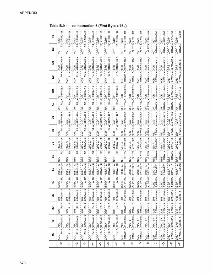
APPENDIX
Table B.9-11 ea Instruction 6 (First Byte = 75H)
0010
2030
4050
6070
8090
A0
B0
C0
D0
E0
F0
+0
AD
DR
0, A
ADD
@R
W0+
d8, A
SU
BR
0, A
SUB
@RW
0+d8
, AS
UB
C A, R
0S
UB
C
A,
@R
W0+
d8N
EG
R0
NE
G A
,@
RW
0+d8
AN
DR
0, A
AND
@R
W0+
d8, A
OR
R0,
AO
R@
RW0+
d8, A
XO
RR
0, A
XO
R@
RW
0+d8
, AN
OT
R0
NO
T@
RW
0+d8
+1
AD
DR
1, A
ADD
@R
W1+
d8, A
SU
BR
1, A
SUB
@RW
1+d8
, AS
UB
C A, R
1S
UB
C
A,
@R
W1+
d8N
EG
R1
NE
G A
,@
RW
1+d8
AN
DR
1, A
AND
@R
W1+
d8, A
OR
R1,
AO
R@
RW1+
d8, A
XO
RR
1, A
XO
R@
RW
1+d8
, AN
OT
R1
NO
T@
RW
1+d8
+2
AD
DR
2, A
ADD
@R
W2+
d8,A
SU
BR
2, A
SUB
@RW
2+d8
,AS
UB
C A, R
2S
UB
C
A,
@R
W2+
d8N
EG
R2
NE
G A
,@
RW
2+d8
AN
DR
2, A
AND
@R
W2+
d8,A
OR
R2,
AO
R@
RW2+
d8,A
XO
RR
2, A
XO
R@
RW
2+d8
,AN
OT
R2
NO
T@
RW
2+d8
+3
AD
DR
3, A
ADD
@R
W3+
d8, A
SU
BR
3, A
SUB
@RW
3+d8
, AS
UB
C A, R
3S
UB
C
A,
@R
W3+
d8N
EG
R3
NE
G A
,@
RW
3+d8
AN
DR
3, A
AND
@R
W3+
d8, A
OR
R3,
AO
R@
RW3+
d8, A
XO
RR
3, A
XO
R@
RW
3+d8
, AN
OT
R3
NO
T@
RW
3+d8
+4
AD
DR
4, A
ADD
@R
W4+
d8, A
SU
BR
4, A
SUB
@RW
4+d8
, AS
UB
C A, R
4S
UB
C
A,
@R
W4+
d8N
EG
R4
NE
G A
,@
RW
4+d8
AN
DR
4, A
AND
@R
W4+
d8, A
OR
R4,
AO
R@
RW4+
d8, A
XO
RR
4, A
XO
R@
RW
4+d8
, AN
OT
R4
NO
T@
RW
4+d8
+5
AD
DR
5, A
ADD
@R
W5+
d8, A
SU
BR
5, A
SUB
@RW
5+d8
, AS
UB
C A, R
5S
UB
C
A,
@R
W5+
d8N
EG
R5
NE
G A
,@
RW
5+d8
AN
DR
5, A
AND
@R
W5+
d8, A
OR
R5,
AO
R@
RW5+
d8, A
XO
RR
5, A
XO
R@
RW
5+d8
, AN
OT
R5
NO
T@
RW
5+d8
+6
AD
DR
6, A
ADD
@R
W6+
d8, A
SU
BR
6, A
SUB
@RW
6+d8
, AS
UB
C A, R
6S
UB
C
A,
@R
W6+
d8N
EG
R6
NE
G A
,@
RW
6+d8
AN
DR
6, A
AND
@R
W6+
d8, A
OR
R6,
AO
R@
RW6+
d8, A
XO
RR
6, A
XO
R@
RW
6+d8
, AN
OT
R6
NO
T@
RW
6+d8
+7
AD
DR
7, A
ADD
@R
W7+
d8, A
SU
BR
7, A
SUB
@RW
7+d8
, AS
UB
C A, R
7S
UB
C
A,
@R
W7+
d8N
EG
R7
NE
G A
,@
RW
7+d8
AN
DR
7, A
AND
@R
W7+
d8, A
OR
R7,
AO
R@
RW7+
d8, A
XO
RR
7, A
XO
R@
RW
7+d8
, AN
OT
R7
NO
T@
RW
7+d8
+8
AD
D@
RW
0, A
ADD
@R
W0+
d16,
AS
UB
@R
W0,
ASU
B@
RW
0+d1
6,A
SU
BC
A, @
RW
0S
UB
C
A,
@R
W0+
d16
NE
G @R
W0
NE
G A
,@
RW
0+d1
6A
ND
@R
W0,
AAN
D@
RW0+
d16,
AO
R@
RW
0, A
OR
@R
W0+
d16,
AX
OR
@R
W0,
AX
OR
@R
W0+
d16,
AN
OT @R
W0
NO
T@
RW
0+d1
6
+9
AD
D@
RW
1, A
ADD
@R
@R
W1+
d16,
AS
UB
@R
W1,
ASU
B@
RW
1+d1
6,A
SU
BC
A, @
RW
1S
UB
C
A,
@R
W1+
d16
NE
G @R
W1
NE
G A
,@
RW
1+d1
6A
ND
@R
W1,
AAN
D@
RW1+
d16,
AO
R@
RW
1, A
OR
@R
W1+
d16,
AX
OR
@R
W1,
AX
OR
@R
W1+
d16,
AN
OT @R
W1
NO
T@
RW
1+d1
6
+A
AD
D@
RW
2, A
ADD
@R
@R
W2+
d16,
AS
UB
@R
W2,
ASU
B@
RW
2+d1
6,A
SU
BC
A, @
RW
2S
UB
C
A,
@R
W2+
d16
NE
G @R
W2
NE
G A
,@
RW
2+d1
6A
ND
@R
W2,
AAN
D@
RW2+
d16,
AO
R@
RW
2, A
OR
@R
W2+
d16,
AX
OR
@R
W2,
AX
OR
@R
W2+
d16,
AN
OT @R
W2
NO
T@
RW
2+d1
6
+B
AD
D@
RW
3, A
ADD
@R
@R
W3+
d16,
AS
UB
@R
W3,
ASU
B@
RW
3+d1
6,A
SU
BC
A, @
RW
3S
UB
C
A,
@R
W3+
d16
NE
G @R
W3
NE
G A
,@
RW
3+d1
6A
ND
@R
W3,
AAN
D@
RW3+
d16,
AO
R@
RW
3, A
OR
@R
W3+
d16,
AX
OR
@R
W3,
AX
OR
@R
W3+
d16,
AN
OT @R
W3
NO
T@
RW
3+d1
6
+C
AD
D@
RW
0+, A
ADD
@R
@R
W0+
RW
7,A
SU
B@
RW
0+, A
SUB
@R
W0+
RW
7,A
SU
BC
A,@
RW
0+SU
BC
A,
@R
W0+
RW7
NE
G@
RW
0+N
EG A
,@
RW0+
RW
7AN
D@
RW
0+, A
AND
@R
W0+
RW
7,A
OR
@R
W0+
, AO
R@
RW
0+R
W7,
AX
OR
@R
W0+
, AX
OR
@R
W0+
RW
7,A
NO
T@
RW
0+NO
T@
RW
0+RW
7
+D
AD
D@
RW
1+, A
ADD
@R
@R
W1+
RW
7,A
SU
B@
RW
1+, A
SUB
@R
W1+
RW
7,A
SU
BC
A,@
RW
1+SU
BC
A,
@R
W1+
RW7
NE
G@
RW
1+N
EG A
,@
RW1+
RW
7AN
D@
RW
1+, A
AND
@R
W1+
RW
7,A
OR
@R
W1+
, AO
R@
RW
1+R
W7,
AX
OR
@R
W1+
, AX
OR
@R
W1+
RW
7,A
NO
T@
RW
1+NO
T@
RW
1+RW
7
+E
AD
D@
RW
2+, A
ADD
@PC
+d16
,AS
UB
@R
W2+
, ASU
B@
PC+d
16,A
SU
BC
A,@
RW
2+S
UB
C
A,
@P
C+
d16
NE
G@
RW
2+N
EG
A,
@P
C+
d16
AND
@R
W2+
, AA
ND
@P
C+d
16,A
OR
@R
W2+
, AO
R@
PC
+d16
,AX
OR
@R
W2+
, AX
OR
@P
C+
d16,
AN
OT
@R
W2+
NO
T@
PC
+d1
6
+F
AD
D@
RW
3+, A
AD
Dad
dr16
, AS
UB
@R
W3+
, AS
UB
addr
16, A
SU
BC
A,@
RW
3+S
UB
C
A,
addr
16N
EG
@R
W3+
NE
G A
,ad
dr16
AND
@R
W3+
, AA
ND
addr
16, A
OR
@R
W3+
, AO
Rad
dr16
, AX
OR
@R
W3+
, AX
OR
addr
16, A
NO
T@
RW
3+N
OT ad
dr16
578

APPENDIX B Instructions
Table B.9-12 ea Instruction 7 (First Byte = 76H)
0010
2030
4050
6070
8090
A0
B0
C0
D0
E0
F0
+0
AD
DW
A, R
W0
AD
DW
A
,@
RW
0+d8
SU
BW
A, R
W0
SU
BW
A
,@
RW
0+d8
AD
DC
WA
, RW
0A
DD
CW
A,
@R
W0+
d8C
MP
WA
, RW
0C
MP
W A
,@
RW
0+d8
AN
DW
A, R
W0
AN
DW
A
,@
RW
0+d8
OR
W A, R
W0
OR
W
A
,@
RW
0+d8
XO
RW
A, R
W0
XO
RW
A
,@
RW
0+d8
DW
BN
ZR
W0,
rD
WB
NZ
@R
W0+
d8,r
+1
AD
DW
A, R
W1
AD
DW
A
,@
RW
1+d8
SU
BW
A, R
W1
SU
BW
A
,@
RW
1+d8
AD
DC
WA
, RW
1A
DD
CW
A,
@R
W1+
d8C
MP
WA
, RW
1C
MP
W A
,@
RW
1+d8
AN
DW
A, R
W1
AN
DW
A
,@
RW
1+d8
OR
W A, R
W1
OR
W
A
,@
RW
1+d8
XO
RW
A, R
W1
XO
RW
A
,@
RW
1+d8
DW
BN
ZR
W1,
rD
WB
NZ
@R
W1+
d8,r
+2
AD
DW
A, R
W2
AD
DW
A
,@
RW
2+d8
SU
BW
A, R
W2
SU
BW
A
,@
RW
2+d8
AD
DC
WA
, RW
2A
DD
CW
A,
@R
W2+
d8C
MP
WA
, RW
2C
MP
W A
,@
RW
2+d8
AN
DW
A, R
W2
AN
DW
A
,@
RW
2+d8
OR
W A, R
W2
OR
W
A
,@
RW
2+d8
XO
RW
A, R
W2
XO
RW
A
,@
RW
2+d8
DW
BN
ZR
W2,
rD
WB
NZ
@R
W2+
d8,r
+3
AD
DW
A, R
W3
AD
DW
A
,@
RW
3+d8
SU
BW
A, R
W3
SU
BW
A
,@
RW
3+d8
AD
DC
WA
, RW
3A
DD
CW
A,
@R
W3+
d8C
MP
WA
, RW
3C
MP
W A
,@
RW
3+d8
AN
DW
A, R
W3
AN
DW
A
,@
RW
3+d8
OR
W A, R
W3
OR
W
A
,@
RW
3+d8
XO
RW
A, R
W3
XO
RW
A
,@
RW
3+d8
DW
BN
ZR
W3,
rD
WB
NZ
@R
W3+
d8,r
+4
AD
DW
A, R
W4
AD
DW
A
,@
RW
4+d8
SU
BW
A, R
W4
SU
BW
A
,@
RW
4+d8
AD
DC
WA
, RW
4A
DD
CW
A,
@R
W4+
d8C
MP
WA
, RW
4C
MP
W A
,@
RW
4+d8
AN
DW
A, R
W4
AN
DW
A
,@
RW
4+d8
OR
W A, R
W4
OR
W
A
,@
RW
4+d8
XO
RW
A, R
W4
XO
RW
A
,@
RW
4+d8
DW
BN
ZR
W4,
rD
WB
NZ
@R
W4+
d8,r
+5
AD
DW
A, R
W5
AD
DW
A
,@
RW
5+d8
SU
BW
A, R
W5
SU
BW
A
,@
RW
5+d8
AD
DC
WA
, RW
5A
DD
CW
A,
@R
W5+
d8C
MP
WA
, RW
5C
MP
W A
,@
RW
5+d8
AN
DW
A, R
W5
AN
DW
A
,@
RW
5+d8
OR
W A, R
W5
OR
W
A
,@
RW
5+d8
XO
RW
A, R
W5
XO
RW
A
,@
RW
5+d8
DW
BN
ZR
W5,
rD
WB
NZ
@R
W5+
d8,r
+6
AD
DW
A, R
W6
AD
DW
A
,@
RW
6+d8
SU
BW
A, R
W6
SU
BW
A
,@
RW
6+d8
AD
DC
WA
, RW
6A
DD
CW
A,
@R
W6+
d8C
MP
WA
, RW
6C
MP
W A
,@
RW
6+d8
AN
DW
A, R
W6
AN
DW
A
,@
RW
6+d8
OR
W A, R
W6
OR
W
A
,@
RW
6+d8
XO
RW
A, R
W6
XO
RW
A
,@
RW
6+d8
DW
BN
ZR
W6,
rD
WB
NZ
@R
W6+
d8,r
+7
AD
DW
A, R
W7
AD
DW
A
,@
RW
7+d8
SU
BW
A, R
W7
SU
BW
A
,@
RW
7+d8
AD
DC
WA
, RW
7A
DD
CW
A,
@R
W7+
d8C
MP
WA
, RW
7C
MP
W A
,@
RW
7+d8
AN
DW
A, R
W7
AN
DW
A
,@
RW
7+d8
OR
W A, R
W7
OR
W
A
,@
RW
7+d8
XO
RW
A, R
W7
XO
RW
A
,@
RW
7+d8
DW
BN
ZR
W7,
rD
WB
NZ
@R
W7+
d8,r
+8
AD
DW
A,@
RW
0A
DD
W
A,
@R
W0+
d16
SU
BW
A,@
RW
0S
UB
W
A,
@R
W0+
d16
AD
DC
WA
,@R
W0
AD
DC
W A
,@
RW
0+d1
6C
MP
WA
,@R
W0
CM
PW
A,
@R
W0+
d16
AN
DW
A,@
RW
0A
ND
W
A,
@R
W0+
d16
OR
WA
,@R
W0
OR
W
A
,@
RW
0+d1
6X
OR
WA
,@R
W0
XO
RW
A
,@
RW
0+d1
6D
WB
NZ
@R
W0,
rD
WBN
Z@
RW0+
d16,
r
+9
AD
DW
A,@
RW
1A
DD
W
A,
@R
W1+
d16
SU
BW
A,@
RW
1S
UB
W
A,
@R
W1+
d16
AD
DC
WA
,@R
W1
AD
DC
W A
,@
RW
1+d1
6C
MP
WA
,@R
W1
CM
PW
A,
@R
W1+
d16
AN
DW
A,@
RW
1A
ND
W
A,
@R
W1+
d16
OR
WA
,@R
W1
OR
W
A
,@
RW
1+d1
6X
OR
WA
,@R
W1
XO
RW
A
,@
RW
1+d1
6D
WB
NZ
@R
W1,
rD
WBN
Z@
RW1+
d16,
r
+A
AD
DW
A,@
RW
2A
DD
W
A,
@R
W2+
d16
SU
BW
A,@
RW
2S
UB
W
A,
@R
W2+
d16
AD
DC
WA
,@R
W2
AD
DC
W A
,@
RW
2+d1
6C
MP
WA
,@R
W2
CM
PW
A,
@R
W2+
d16
AN
DW
A,@
RW
2A
ND
W
A,
@R
W2+
d16
OR
WA
,@R
W2
OR
W
A
,@
RW
2+d1
6X
OR
WA
,@R
W2
XO
RW
A
,@
RW
2+d1
6D
WB
NZ
@R
W2,
rD
WBN
Z@
RW2+
d16,
r
+B
AD
DW
A,@
RW
3A
DD
W
A,
@R
W3+
d16
SU
BW
A,@
RW
3S
UB
W
A,
@R
W3+
d16
AD
DC
WA
,@R
W3
AD
DC
W A
,@
RW
3+d1
6C
MP
WA
,@R
W3
CM
PW
A,
@R
W3+
d16
AN
DW
A,@
RW
3A
ND
W
A,
@R
W3+
d16
OR
WA
,@R
W3
OR
W
A
,@
RW
3+d1
6X
OR
WA
,@R
W3
XO
RW
A
,@
RW
3+d1
6D
WB
NZ
@R
W3,
rD
WBN
Z@
RW3+
d16,
r
+C
AD
DW
A,@
RW
0+AD
DW
A,
@R
W0+
RW7
SU
BW
A,@
RW
0+SU
BW
A,@
RW
0+RW
7A
DD
CW
A,@
RW
0+AD
DC
W A
,@
RW0+
RW
7C
MP
WA
,@R
W0+
CM
PW A
,@
RW
0+RW
7A
ND
WA
,@R
W0+
AND
W
A,@
RW
0+RW
7O
RW
A,@
RW
0+O
RW
A
,@
RW0+
RW
7X
OR
WA
,@R
W0+
XOR
W
A,@
RW0+
RW7
DW
BN
Z@
RW
0+, r
DW
BNZ
@RW
0+R
W7,
r
+D
AD
DW
A,@
RW
1+AD
DW
A,
@R
W1+
RW7
SU
BW
A,@
RW
1+SU
BW
A,@
RW
1+RW
7A
DD
CW
A,@
RW
1+AD
DC
W A
,@
RW1+
RW
7C
MP
WA
,@R
W1+
CM
PW A
,@
RW
1+RW
7A
ND
WA
,@R
W1+
AND
W
A,@
RW
1+RW
7O
RW
A,@
RW
1+O
RW
A
,@
RW1+
RW
7X
OR
WA
,@R
W1+
XOR
W
A,@
RW1+
RW7
DW
BN
Z@
RW
1+, r
DW
BNZ
@RW
1+R
W7,
r
+E
AD
DW
A,@
RW
2+A
DD
W
A,
@P
C+
d16
SU
BW
A,@
RW
2+S
UB
W
A,
@P
C+
d16
AD
DC
WA
,@R
W2+
AD
DC
W A
,@
PC
+d1
6C
MP
WA
,@R
W2+
CM
PW
A,
@P
C+
d16
AN
DW
A,@
RW
2+A
ND
W
A,
@P
C+
d16
OR
WA
,@R
W2+
OR
W
A
,@
PC
+d1
6,X
OR
WA
,@R
W2+
XO
RW
A
,@
PC
+d1
6D
WB
NZ
@R
W2+
, rD
WB
NZ
@P
C+
d16,
r
+F
AD
DW
A,@
RW
3+A
DD
W
A,
addr
16
SU
BW
A,@
RW
3+S
UB
W
A,
addr
16
AD
DC
WA
,@R
W3+
AD
DC
W A
,ad
dr 1
6C
MP
WA
,@R
W3+
CM
PW
A,
addr
16
AN
DW
A,@
RW
3+A
ND
W
A,
addr
16
OR
WA
,@R
W3+
OR
W
A
,ad
dr r
16X
OR
WA
,@R
W3+
XO
RW
A
,ad
dr 1
6D
WB
NZ
@R
W3+
, rD
WB
NZ
addr
r16
, r
579

APPENDIX
Table B.9-13 ea Instruction 8 (First Byte = 77H)
0010
2030
4050
6070
8090
A0
B0
C0
D0
E0
F0
+0
AD
DW
RW
0, A
ADD
W@
RW0+
d8, A
SU
BW
RW
0, A
SUBW
@RW
0+d8
, AS
UB
CW
A, R
W0
SU
BC
W A
,@
RW
0+d8
NE
GW R
W0
NE
GW
@R
W0+
d8A
ND
WR
W0,
AAN
DW@
RW
0+d8
, AO
RW RW
0, A
ORW
@RW
0+d8
, AX
OR
WR
W0,
AXO
RW@
RW0+
d8, A
NO
TW R
W0
NO
TW
@R
W0+
d8
+1
AD
DW
RW
1, A
ADD
W@
RW1+
d8, A
SU
BW
RW
1, A
SUBW
@RW
1+d8
, AS
UB
CW
A, R
W1
SU
BC
W A
,@
RW
1+d8
NE
GW R
W1
NE
GW
@R
W1+
d8A
ND
WR
W1,
AAN
DW@
RW
1+d8
, AO
RW RW
1, A
ORW
@RW
1+d8
, AX
OR
WR
W1,
AXO
RW@
RW1+
d8, A
NO
TW R
W1
NO
TW
@R
W1+
d8
+2
AD
DW
RW
2, A
ADD
W@
RW2+
d8,A
SU
BW
RW
2, A
SUBW
@RW
2+d8
,AS
UB
CW
A, R
W2
SU
BC
W A
,@
RW
2+d8
NE
GW R
W2
NE
GW
@R
W2+
d8A
ND
WR
W2,
AAN
DW@
RW
2+d8
,AO
RW RW
2, A
OR
W@
RW
2+d8
,AX
OR
WR
W2,
AXO
RW@
RW2+
d8,A
NO
TW R
W2
NO
TW
@R
W2+
d8
+3
AD
DW
RW
3, A
ADD
W@
RW3+
d8, A
SU
BW
RW
3, A
SUBW
@RW
3+d8
, AS
UB
CW
A, R
W3
SU
BC
W A
,@
RW
3+d8
NE
GW R
W3
NE
GW
@R
W3+
d8A
ND
WR
W3,
AAN
DW@
RW
3+d8
, AO
RW RW
3, A
ORW
@RW
3+d8
, AX
OR
WR
W3,
AXO
RW@
RW3+
d8, A
NO
TW R
W3
NO
TW
@R
W3+
d8
+4
AD
DW
RW
4, A
ADD
W@
RW4+
d8, A
SU
BW
RW
4, A
SUBW
@RW
4+d8
, AS
UB
CW
A, R
W4
SU
BC
W A
,@
RW
4+d8
NE
GW R
W4
NE
GW
@R
W4+
d8A
ND
WR
W4,
AAN
DW@
RW
4+d8
, AO
RW RW
4, A
ORW
@RW
4+d8
, AX
OR
WR
W4,
AXO
RW@
RW4+
d8, A
NO
TW R
W4
NO
TW
@R
W4+
d8
+5
AD
DW
RW
5, A
ADD
W@
RW5+
d8, A
SU
BW
RW
5, A
SUBW
@RW
5+d8
, AS
UB
CW
A, R
W5
SU
BC
W A
,@
RW
5+d8
NE
GW R
W5
NE
GW
@R
W5+
d8A
ND
WR
W5,
AAN
DW@
RW
5+d8
, AO
RW RW
5, A
ORW
@RW
5+d8
, AX
OR
WR
W5,
AXO
RW@
RW5+
d8, A
NO
TW R
W5
NO
TW
@R
W5+
d8
+6
AD
DW
RW
6, A
ADD
W@
RW6+
d8, A
SU
BW
RW
6, A
SUBW
@RW
6+d8
, AS
UB
CW
A, R
W6
SU
BC
W A
,@
RW
6+d8
NE
GW R
W6
NE
GW
@R
W6+
d8A
ND
WR
W6,
AAN
DW@
RW
6+d8
, AO
RW RW
6, A
ORW
@RW
6+d8
, AX
OR
WR
W6,
AXO
RW@
RW6+
d8, A
NO
TW R
W6
NO
TW
@R
W6+
d8
+7
AD
DW
RW
7, A
ADD
W@
RW7+
d8, A
SU
BW
RW
7, A
SUBW
@RW
7+d8
, AS
UB
CW
A, R
W7
SU
BC
W A
,@
RW
7+d8
NE
GW R
W7
NE
GW
@R
W7+
d8A
ND
WR
W7,
AAN
DW@
RW
7+d8
, AO
RW RW
7, A
ORW
@RW
7+d8
, AX
OR
WR
W7,
AXO
RW@
RW7+
d8, A
NO
TW R
W7
NO
TW
@R
W7+
d8
+8
AD
DW
@R
W0,
AAD
DW
@RW
0+d1
6,A
SU
BW
@R
W0,
ASU
BW@
RW0+
d16,
AS
UB
CW
A, @
RW
0S
UB
CW
A,
@R
W0+
d16
NE
GW
@R
W0
NE
GW
@R
W0+
d16
AN
DW
@R
W0,
AAN
DW@
RW0+
d16,
AO
RW
@R
W0,
AO
RW
@R
W0+
d16,
AX
OR
W@
RW
0, A
XORW
@RW
0+d1
6,A
NO
TW
@R
W0
NO
TW@
RW
0+d1
6
+9
AD
DW
@R
W1,
AAD
DW
@RW
1+d1
6,A
SU
BW
@R
W1,
ASU
BW@
RW1+
d16,
AS
UB
CW
A, @
RW
1S
UB
CW
A,
@R
W1+
d16
NE
GW
@R
W1
NE
GW
@R
W1+
d16
AN
DW
@R
W1,
AAN
DW@
RW1+
d16,
AO
RW
@R
W1,
AO
RW
@R
W1+
d16,
AX
OR
W@
RW
1, A
XORW
@RW
1+d1
6,A
NO
TW
@R
W1
NO
TW@
RW
1+d1
6
+A
AD
DW
@R
W2,
AAD
DW
@RW
2+d1
6,A
SU
BW
@R
W2,
ASU
BW@
RW2+
d16,
AS
UB
CW
A, @
RW
2S
UB
CW
A,
@R
W2+
d16
NE
GW
@R
W2
NE
GW
@R
W2+
d16
AN
DW
@R
W2,
AAN
DW@
RW2+
d16,
AO
RW
@R
W2,
AO
RW@
RW2+
d16,
AX
OR
W@
RW
2, A
XORW
@RW
2+d1
6,A
NO
TW
@R
W2
NO
TW@
RW
2+d1
6
+B
AD
DW
@R
W3,
AAD
DW
@RW
3+d1
6,A
SU
BW
@R
W3,
ASU
BW@
RW3+
d16,
AS
UB
CW
A, @
RW
3S
UB
CW
A,
@R
W3+
d16
NE
GW
@R
W3
NE
GW
@R
W3+
d16
AN
DW
@R
W3,
AAN
DW@
RW3+
d16,
AO
RW
@R
W3,
AO
RW@
RW3+
d16,
AX
OR
W@
RW
3, A
XORW
@RW
3+d1
6,A
NO
TW
@R
W3
NO
TW@
RW
3+d1
6
+C
ADDW
@RW
0+, A
ADD
W@
RW
0+R
W7,
AS
UB
W@
RW
0+, A
SUBW
@R
W0+
RW
7,A
SU
BC
WA
,@R
W0+
SUBC
W A
,@
RW0+
RW
7N
EG
W@
RW
0+N
EGW
@R
W0+
RW7
AN
DW
@R
W0+
, AAN
DW@
RW0+
RW7,
AO
RW
@R
W0+
, AO
RW
@R
W0+
RW
7,A
XO
RW
@R
W0+
, AX
OR
W@
RW
0+R
W7,
AN
OT
W@
RW
0+N
OTW
@R
W0+
RW7
+D
ADDW
@RW
1+, A
ADD
W@
RW
1+R
W7,
AS
UB
W@
RW
1+, A
SUBW
@R
W1+
RW
7,A
SU
BC
WA
,@R
W1+
SUBC
W A
,@
RW1+
RW
7N
EG
W@
RW
1+N
EGW
@R
W1+
RW7
AN
DW
@R
W1+
, AAN
DW@
RW1+
RW7,
AO
RW
@R
W1+
, AO
RW
@R
W1+
RW
7,A
XO
RW
@R
W1+
, AX
OR
W@
RW
1+R
W7,
AN
OT
W@
RW
1+N
OTW
@R
W1+
RW7
+E
ADDW
@RW
2+, A
ADD
W@
PC+d
16,A
SU
BW
@R
W2+
, ASU
BW@
PC+d
16,A
SU
BC
WA
,@R
W2+
SU
BC
W A
,@
PC
+d1
6N
EG
W@
RW
2+N
EG
W@
PC
+d1
6A
ND
W@
RW
2+, A
AN
DW
@P
C+d
16,A
OR
W@
RW
2+, A
OR
W@
PC
+d16
,AX
OR
W@
RW
2+, A
XO
RW
@P
C+d
16,A
NO
TW
@R
W2+
NO
TW
@P
C+
d16
+F
ADDW
@RW
3+, A
AD
DW
addr
16, A
SU
BW
@R
W3+
, AS
UB
Wad
dr16
, AS
UB
CW
A,@
RW
3+S
UB
CW
A,
addr
16N
EG
W@
RW
3+N
EG
W addr
16A
ND
W@
RW
3+, A
AN
DW
addr
16, A
OR
W@
RW
3+, A
OR
Wad
dr16
, AX
OR
W@
RW
3+, A
XO
RW
addr
16, A
NO
TW
@R
W3+
NO
TW ad
dr16
580
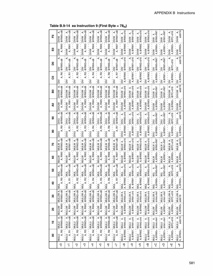
APPENDIX B Instructions
Table B.9-14 ea Instruction 9 (First Byte = 78H)
0010
2030
4050
6070
8090
A0
B0
C0
D0
E0
F0
+0
MU
LU A, R
0M
ULU
A
,@
RW
0+d8
MU
LUW
A, R
W0
MU
LUW
A,
@R
W0+
d8M
UL A
, R0
MU
L
A,
@R
W0+
d8M
ULW A, R
W0
MU
LW A
,@
RW
0+d8
DIV
U A, R
0D
IVU
A,
@R
W0+
d8D
IVU
WA
, RW
0D
IVU
W
A,
@R
W0+
d8D
IVA
, R0
DIV
A
,@
RW
0+d8
DIV
W A, R
W0
DIV
W
A,
@R
W0+
d8
+1
MU
LU A, R
1M
ULU
A
,@
RW
1+d8
MU
LUW
A, R
W1
MU
LUW
A,
@R
W1+
d8M
UL A
, R1
MU
L
A,
@R
W1+
d8M
ULW A, R
W1
MU
LW A
,@
RW
1+d8
DIV
U A, R
1D
IVU
A,
@R
W1+
d8D
IVU
WA
, RW
1D
IVU
W
A,
@R
W1+
d8D
IVA
, R1
DIV
A
,@
RW
1+d8
DIV
W A, R
W1
DIV
W
A,
@R
W1+
d8
+2
MU
LU A, R
2M
ULU
A
,@
RW
2+d8
MU
LUW
A, R
W2
MU
LUW
A,
@R
W2+
d8M
UL A
, R2
MU
L
A,
@R
W2+
d8M
ULW A, R
W2
MU
LW A
,@
RW
2+d8
DIV
U A, R
2D
IVU
A,
@R
W2+
d8D
IVU
WA
, RW
2D
IVU
W
A,
@R
W2+
d8D
IVA
, R2
DIV
A
,@
RW
2+d8
DIV
W A, R
W2
DIV
W
A,
@R
W2+
d8
+3
MU
LU A, R
3M
ULU
A
,@
RW
3+d8
MU
LUW
A, R
W3
MU
LUW
A,
@R
W3+
d8M
UL A
, R3
MU
L
A,
@R
W3+
d8M
ULW A, R
W3
MU
LW A
,@
RW
3+d8
DIV
U A, R
3D
IVU
A,
@R
W3+
d8D
IVU
WA
, RW
3D
IVU
W
A,
@R
W3+
d8D
IVA
, R3
DIV
A
,@
RW
3+d8
DIV
W A, R
W3
DIV
W
A,
@R
W3+
d8
+4
MU
LU A, R
4M
ULU
A
,@
RW
4+d8
MU
LUW
A, R
W4
MU
LUW
A,
@R
W4+
d8M
UL A
, R4
MU
L
A,
@R
W4+
d8M
ULW A, R
W4
MU
LW A
,@
RW
4+d8
DIV
U A, R
4D
IVU
A,
@R
W4+
d8D
IVU
WA
, RW
4D
IVU
W
A,
@R
W4+
d8D
IVA
, R4
DIV
A
,@
RW
4+d8
DIV
W A, R
W4
DIV
W
A,
@R
W4+
d8
+5
MU
LU A, R
5M
ULU
A
,@
RW
5+d8
MU
LUW
A, R
W5
MU
LUW
A,
@R
W5+
d8M
UL A
, R5
MU
L
A,
@R
W5+
d8M
ULW A, R
W5
MU
LW A
,@
RW
5+d8
DIV
U A, R
5D
IVU
A,
@R
W5+
d8D
IVU
WA
, RW
5D
IVU
W
A,
@R
W5+
d8D
IVA
, R5
DIV
A
,@
RW
5+d8
DIV
W A, R
W5
DIV
W
A,
@R
W5+
d8
+6
MU
LU A, R
6M
ULU
A
,@
RW
6+d8
MU
LUW
A, R
W6
MU
LUW
A,
@R
W6+
d8M
UL A
, R6
MU
L
A,
@R
W6+
d8M
ULW A, R
W6
MU
LW A
,@
RW
6+d8
DIV
U A, R
6D
IVU
A,
@R
W6+
d8D
IVU
WA
, RW
6D
IVU
W
A,
@R
W6+
d8D
IVA
, R6
DIV
A
,@
RW
6+d8
DIV
W A, R
W6
DIV
W
A,
@R
W6+
d8
+7
MU
LU A, R
7M
ULU
A
,@
RW
7+d8
MU
LUW
A, R
W7
MU
LUW
A,
@R
W7+
d8M
UL A
, R7
MU
L
A,
@R
W7+
d8M
ULW A, R
W7
MU
LW A
,@
RW
7+d8
DIV
U A, R
7D
IVU
A,
@R
W7+
d8D
IVU
WA
, RW
7D
IVU
W
A,
@R
W7+
d8D
IVA
, R7
DIV
A
,@
RW
7+d8
DIV
W A, R
W7
DIV
W
A,
@R
W7+
d8
+8
MU
LUA
,@R
W0
MU
LU
A,
@R
W0+
d16
MU
LUW
A,@
RW
0M
ULU
W A
,@
RW
0+d1
6M
UL
A, @
RW
0M
UL
A
,@
RW
0+d1
6M
ULW
A,@
RW
0M
ULW
A,
@R
W0+
d16
DIV
UA
,@R
W0
DIV
U
A
,@
RW
0+d1
6D
IVU
WA
,@R
W0
DIV
UW
A
,@
RW
0+d1
6D
IV A,@
RW
0D
IV
A,
@R
W0+
d16
DIV
WA
,@R
W0
DIV
W
A,
@R
W0+
d16
+9
MU
LUA
,@R
W1
MU
LU
A,
@R
W1+
d16
MU
LUW
A,@
RW
1M
ULU
W A
,@
RW
1+d1
6M
UL
A, @
RW
1M
UL
A
,@
RW
1+d1
6M
ULW
A,@
RW
1M
ULW
A,
@R
W1+
d16
DIV
UA
,@R
W1
DIV
U
A
,@
RW
1+d1
6D
IVU
WA
,@R
W1
DIV
UW
A
,@
RW
1+d1
6D
IV A,@
RW
1D
IV
A,
@R
W1+
d16
DIV
WA
,@R
W1
DIV
W
A,
@R
W1+
d16
+A
MU
LUA
,@R
W2
MU
LU
A,
@R
W2+
d16
MU
LUW
A,@
RW
2M
ULU
W A
,@
RW
2+d1
6M
UL
A, @
RW
2M
UL
A
,@
RW
2+d1
6M
ULW
A,@
RW
2M
ULW
A,
@R
W2+
d16
DIV
UA
,@R
W2
DIV
U
A
,@
RW
2+d1
6D
IVU
WA
,@R
W2
DIV
UW
A
,@
RW
2+d1
6D
IV A,@
RW
2D
IV
A,
@R
W2+
d16
DIV
WA
,@R
W2
DIV
W
A,
@R
W2+
d16
+B
MU
LUA
,@R
W3
MU
LU
A,
@R
W3+
d16
MU
LUW
A,@
RW
3M
ULU
W A
,@
RW
3+d1
6M
UL
A, @
RW
3M
UL
A
,@
RW
3+d1
6M
ULW
A,@
RW
3M
ULW
A,
@R
W3+
d16
DIV
UA
,@R
W3
DIV
U
A
,@
RW
3+d1
6D
IVU
WA
,@R
W3
DIV
UW
A
,@
RW
3+d1
6D
IV A,@
RW
3D
IV
A,
@R
W3+
d16
DIV
WA
,@R
W3
DIV
W
A,
@R
W3+
d16
+C
MU
LUA
,@R
W0+
MU
LU
A,
@R
W0+
RW
7M
ULU
WA
,@R
W0+
MU
LUW
A,
@R
W0+
RW
7M
UL
A,@
RW
0+M
UL
A
,@
RW
0+RW
7M
ULW
A,@
RW
0+M
ULW
A,
@RW
0+R
W7
DIV
UA
,@R
W0+
DIV
U
A,
@R
W0+
RW7
DIV
UW
A,@
RW
0+D
IVUW
A,
@R
W0+
RW7
DIV A,@
RW
0+D
IV
A,
@R
W0+
RW
7D
IVW
A,@
RW
0+D
IVW
A
,@
RW
0+RW
7
+D
MU
LUA
,@R
W1+
MU
LU
A,
@R
W1+
RW
7M
ULU
WA
,@R
W1+
MU
LUW
A,
@R
W1+
RW
7M
UL
A,@
RW
1+M
UL
A
,@
RW
1+RW
7M
ULW
A,@
RW
1+M
ULW
A,
@RW
1+R
W7
DIV
UA
,@R
W1+
DIV
U
A,
@R
W1+
RW7
DIV
UW
A,@
RW
1+D
IVUW
A,
@R
W1+
RW7
DIV A,@
RW
1+D
IV
A,
@R
W1+
RW
7D
IVW
A,@
RW
1+D
IVW
A
,@
RW
1+RW
7
+E
MU
LUA
,@R
W2+
MU
LU
A,
@P
C+
d16
MU
LUW
A,@
RW
2+M
ULU
W A
,@
PC
+d1
6M
UL
A,@
RW
2+M
UL
A
,@
PC
+d1
6M
ULW
A,@
RW
2+M
ULW
A,
@P
C+
d16
DIV
UA
,@R
W2+
DIV
U
A
,@
PC
+d1
6D
IVU
WA
,@R
W2+
DIV
UW
A
,@
PC
+d1
6D
IV A,@
RW
2+D
IV
A,
@P
C+
d16
DIV
WA
,@R
W2+
DIV
W
A,
@P
C+
d16
+F
MU
LUA
, @R
W3+
MU
LU
A,
addr
16M
ULU
WA
,@R
W3+
MU
LUW
A,
addr
16M
UL
A,@
RW
3+M
UL
A
,ad
dr16
MU
LWA
,@R
W3+
MU
LW A
,ad
dr16
DIV
UA
,@R
W3+
DIV
U
A
,ad
dr16
DIV
UW
A,@
RW
3+D
IVU
W
A,
addr
16D
IV A,@
RW
3+D
IV
A,
addr
16D
IVW
A,@
RW
3+D
IVW
A
,ad
dr16
581

APPENDIX
Table B.9-15 MOVEA RWi, ea Instruction (First Byte = 79H)
0010
2030
4050
6070
8090
A0
B0
C0
D0
E0
F0
+0
MO
VE
AR
W0,
RW
0M
OVE
A RW
0,@
RW0+
d8M
OV
EA
RW
1,R
W0
MO
VEA
RW1
,@R
W0+
d8M
OV
EA
RW
2,R
W0
MO
VEA
RW2
,@RW
0+d8
MO
VE
AR
W3,
RW
0M
OVE
A RW
3,@
RW0+
d8M
OV
EA
RW
4,R
W0
MO
VEA
RW4
,@RW
0+d8
MO
VE
AR
W5,
RW
0M
OV
EA
RW
5,@
RW
0+d8
MO
VE
AR
W6,
RW
0M
OVE
A RW
6,@
RW
0+d8
MO
VE
AR
W7,
RW
0M
OVE
A RW
7,@
RW0+
d8
+1
MO
VE
AR
W0,
RW
1M
OVE
A RW
0,@
RW1+
d8M
OV
EA
RW
1,R
W1
MO
VEA
RW1
,@R
W1+
d8M
OV
EA
RW
2,R
W1
MO
VEA
RW2
,@RW
1+d8
MO
VE
AR
W3,
RW
1M
OVE
A RW
3,@
RW1+
d8M
OV
EA
RW
4,R
W1
MO
VEA
RW4
,@RW
1+d8
MO
VE
AR
W5,
RW
1M
OV
EA
RW
5,@
RW
1+d8
MO
VE
AR
W6,
RW
1M
OVE
A RW
6,@
RW
1+d8
MO
VE
AR
W7,
RW
1M
OVE
A RW
7,@
RW1+
d8
+2
MO
VE
AR
W0,
RW
2M
OVE
A RW
0,@
RW2+
d8M
OV
EA
RW
1,R
W2
MO
VEA
RW1
,@R
W2+
d8M
OV
EA
RW
2,R
W2
MO
VEA
RW2
,@RW
2+d8
MO
VE
AR
W3,
RW
2M
OVE
A RW
3,@
RW2+
d8M
OV
EA
RW
4,R
W2
MO
VEA
RW4
,@RW
2+d8
MO
VE
AR
W5,
RW
2M
OV
EA
RW
5,@
RW
2+d8
MO
VE
AR
W6,
RW
2M
OVE
A RW
6,@
RW
2+d8
MO
VE
AR
W7,
RW
2M
OVE
A RW
7,@
RW2+
d8
+3
MO
VE
AR
W0,
RW
3M
OVE
A RW
0,@
RW3+
d8M
OV
EA
RW
1,R
W3
MO
VEA
RW1
,@R
W3+
d8M
OV
EA
RW
2,R
W3
MO
VEA
RW2
,@RW
3+d8
MO
VE
AR
W3,
RW
3M
OVE
A RW
3,@
RW3+
d8M
OV
EA
RW
4,R
W3
MO
VEA
RW4
,@RW
3+d8
MO
VE
AR
W5,
RW
3M
OV
EA
RW
5,@
RW
3+d8
MO
VE
AR
W6,
RW
3M
OVE
A RW
6,@
RW
3+d8
MO
VE
AR
W7,
RW
3M
OVE
A RW
7,@
RW3+
d8
+4
MO
VE
AR
W0,
RW
4M
OVE
A RW
0,@
RW4+
d8M
OV
EA
RW
1,R
W4
MO
VEA
RW1
,@R
W4+
d8M
OV
EA
RW
2,R
W4
MO
VEA
RW2
,@RW
4+d8
MO
VE
AR
W3,
RW
4M
OVE
A RW
3,@
RW4+
d8M
OV
EA
RW
4,R
W4
MO
VEA
RW4
,@RW
4+d8
MO
VE
AR
W5,
RW
4M
OV
EA
RW
5,@
RW
4+d8
MO
VE
AR
W6,
RW
4M
OVE
A RW
6,@
RW
4+d8
MO
VE
AR
W7,
RW
4M
OVE
A RW
7,@
RW4+
d8
+5
MO
VE
AR
W0,
RW
5M
OVE
A RW
0,@
RW5+
d8M
OV
EA
RW
1,R
W5
MO
VEA
RW1
,@R
W5+
d8M
OV
EA
RW
2,R
W5
MO
VEA
RW2
,@RW
5+d8
MO
VE
AR
W3,
RW
5M
OVE
A RW
3,@
RW5+
d8M
OV
EA
RW
4,R
W5
MO
VEA
RW4
,@RW
5+d8
MO
VE
AR
W5,
RW
5M
OV
EA
RW
5,@
RW
5+d8
MO
VE
AR
W6,
RW
5M
OVE
A RW
6,@
RW
5+d8
MO
VE
AR
W7,
RW
5M
OVE
A RW
7,@
RW5+
d8
+6
MO
VE
AR
W0,
RW
6M
OVE
A RW
0,@
RW6+
d8M
OV
EA
RW
1,R
W6
MO
VEA
RW1
,@R
W6+
d8M
OV
EA
RW
2,R
W6
MO
VEA
RW2
,@RW
6+d8
MO
VE
AR
W3,
RW
6M
OVE
A RW
3,@
RW6+
d8M
OV
EA
RW
4,R
W6
MO
VEA
RW4
,@RW
6+d8
MO
VE
AR
W5,
RW
6M
OV
EA
RW
5,@
RW
6+d8
MO
VE
AR
W6,
RW
6M
OVE
A RW
6,@
RW
6+d8
MO
VE
AR
W7,
RW
6M
OVE
A RW
7,@
RW6+
d8
+7
MO
VE
AR
W0,
RW
7M
OVE
A RW
0,@
RW7+
d8M
OV
EA
RW
1,R
W7
MO
VEA
RW1
,@R
W7+
d8M
OV
EA
RW
2,R
W7
MO
VEA
RW2
,@RW
7+d8
MO
VE
AR
W3,
RW
7M
OVE
A RW
3,@
RW7+
d8M
OV
EA
RW
4,R
W7
MO
VEA
RW4
,@RW
7+d8
MO
VE
AR
W5,
RW
7M
OV
EA
RW
5,@
RW
7+d8
MO
VE
AR
W6,
RW
7M
OVE
A RW
6,@
RW
7+d8
MO
VE
AR
W7,
RW
7M
OVE
A RW
7,@
RW7+
d8
+8
MO
VE
AR
W0,
@R
W0
MO
VEA
RW0
,@RW
0+d1
6M
OV
EA
RW
1,@
RW
0M
OVE
A RW
1,@
RW
0+d1
6M
OV
EA
RW
2,@
RW
0M
OVE
A RW
2,@
RW0+
d16
MO
VE
AR
W3,
@R
W0
MO
VEA
RW3
,@RW
0+d1
6M
OV
EA
RW
4,@
RW
0M
OVE
A RW
4,@
RW0+
d16
MO
VE
AR
W5,
@R
W0
MO
VE
A R
W5
,@R
W0+
d16
MO
VE
AR
W6,
@R
W0
MO
VEA
RW6
,@R
W0+
d16
MO
VE
AR
W7,
@R
W0
MO
VEA
RW7
,@RW
0+d1
6
+9
MO
VE
AR
W0,
@R
W1
MO
VEA
RW0
,@RW
1+d1
6M
OV
EA
RW
1,@
RW
1M
OVE
A RW
1,@
RW
1+d1
6M
OV
EA
RW
2,@
RW
1M
OVE
A RW
2,@
RW1+
d16
MO
VE
AR
W3,
@R
W1
MO
VEA
RW3
,@RW
1+d1
6M
OV
EA
RW
4,@
RW
1M
OVE
A RW
4,@
RW1+
d16
MO
VE
AR
W5,
@R
W1
MO
VE
A R
W5
,@R
W1+
d16
MO
VE
AR
W6,
@R
W1
MO
VEA
RW6
,@R
W1+
d16
MO
VE
AR
W7,
@R
W1
MO
VEA
RW7
,@RW
1+d1
6
+A
MO
VE
AR
W0,
@R
W2
MO
VEA
RW0
,@RW
2+d1
6M
OV
EA
RW
1,@
RW
2M
OVE
A RW
1,@
RW
2+d1
6M
OV
EA
RW
2,@
RW
2M
OVE
A RW
2,@
RW2+
d16
MO
VE
AR
W3,
@R
W2
MO
VEA
RW3
,@RW
2+d1
6M
OV
EA
RW
4,@
RW
2M
OVE
A RW
4,@
RW2+
d16
MO
VE
AR
W5,
@R
W2
MO
VE
A R
W5
,@R
W2+
d16
MO
VE
AR
W6,
@R
W2
MO
VEA
RW6
,@R
W2+
d16
MO
VE
AR
W7,
@R
W2
MO
VEA
RW7
,@RW
2+d1
6
+B
MO
VE
AR
W0,
@R
W3
MO
VEA
RW0
,@RW
3+d1
6M
OV
EA
RW
1,@
RW
3M
OVE
A RW
1,@
RW
3+d1
6M
OV
EA
RW
2,@
RW
3M
OVE
A RW
2,@
RW3+
d16
MO
VE
AR
W3,
@R
W3
MO
VEA
RW3
,@RW
3+d1
6M
OV
EA
RW
4,@
RW
3M
OVE
A RW
4,@
RW3+
d16
MO
VE
AR
W5,
@R
W3
MO
VE
A R
W5
,@R
W3+
d16
MO
VE
AR
W6,
@R
W3
MO
VEA
RW6
,@R
W3+
d16
MO
VE
AR
W7,
@R
W3
MO
VEA
RW7
,@RW
3+d1
6
+C
MO
VEA
RW0,
@RW
0+M
OVE
A RW
0,@
RW0+
RW7
MO
VEA
RW1,
@RW
0+M
OVE
A RW
1,@
RW
0+RW
7M
OVE
ARW
2,@
RW0+
MO
VEA
RW2
,@RW
0+RW
7M
OVE
ARW
3,@
RW0+
MO
VEA
RW3
,@RW
0+RW
7M
OVE
ARW
4,@
RW0+
MO
VEA
RW4
,@RW
0+RW
7M
OVE
AR
W5,
@RW
0+M
OV
EA
RW
5,@
RW
0+R
W7
MO
VEA
RW6,
@R
W0+
MO
VEA
RW6
,@R
W0+
RW
7M
OVE
ARW
7,@
RW0+
MO
VEA
RW7
,@RW
0+RW
7
+D
MO
VEA
RW0,
@RW
1+M
OVE
A RW
0,@
RW1+
RW7
MO
VEA
RW1,
@RW
1+M
OVE
A RW
1,@
RW
1+RW
7M
OVE
ARW
2,@
RW1+
MO
VEA
RW2
,@RW
1+RW
7M
OVE
ARW
3,@
RW1+
MO
VEA
RW3
,@RW
1+RW
7M
OVE
ARW
4,@
RW1+
MO
VEA
RW4
,@RW
1+RW
7M
OVE
AR
W5,
@RW
1+M
OV
EA
RW
5,@
RW
1+R
W7
MO
VEA
RW6,
@R
W1+
MO
VEA
RW6
,@R
W1+
RW
7M
OVE
ARW
7,@
RW1+
MO
VEA
RW7
,@RW
1+RW
7
+E
MO
VEA
RW0,
@RW
2+M
OVE
A RW
0,@
PC+d
16M
OVE
ARW
1,@
RW2+
MO
VEA
RW1
,@PC
+d16
MO
VEA
RW2,
@RW
2+M
OVE
A RW
2,@
PC+d
16M
OVE
ARW
3,@
RW2+
MO
VEA
RW3
,@PC
+d16
MO
VEA
RW4,
@RW
2+M
OVE
A RW
4,@
PC+d
16M
OVE
AR
W5,
@RW
2+M
OV
EA
RW
5,@
PC
+d16
MO
VEA
RW6,
@R
W2+
MO
VEA
RW6
,@PC
+d16
MO
VEA
RW7,
@RW
2+M
OVE
A RW
7,@
PC+d
16
+F
MO
VEA
RW0,
@RW
3+M
OV
EA
R
W0,
add
r16
MO
VEA
RW1,
@RW
3+M
OV
EA
R
W1,
add
r16
MO
VEA
RW2,
@RW
3+M
OV
EA
R
W2,
add
r16
MO
VEA
RW3,
@RW
3+M
OV
EA
R
W3,
add
r16
MO
VEA
RW4,
@RW
3+M
OV
EA
R
W4,
add
r16
MO
VEA
RW
5,@
RW3+
MO
VE
A
RW
5, a
ddr1
6M
OVE
ARW
6,@
RW
3+M
OV
EA
R
W6,
add
r16
MO
VEA
RW7@
RW3+
MO
VE
A
RW
7, a
ddr1
6
582

APPENDIX B Instructions
Table B.9-16 MOV Ri, ea Instruction (First Byte = 7AH)
0010
2030
4050
6070
8090
A0
B0
C0
D0
E0
F0
+0
MO
V R0,
R0
MO
V
R0,
@R
W0+
d8M
OV R
1, R
0M
OV
R
1,@
RW
0+d8
MO
V R2,
R0
MO
V
R2,
@R
W0+
d8M
OV R
3, R
0M
OV
R
3,@
RW
0+d8
MO
V R4,
R0
MO
V
R4,
@R
W0+
d8M
OV R
5, R
0M
OV
R
5,@
RW
0+d8
MO
V R6,
R0
MO
V
R6,
@R
W0+
d8M
OV R
7, R
0M
OV
R
7,@
RW
0+d8
+1
MO
V R0,
R1
MO
V
R0,
@R
W1+
d8M
OV R
1, R
1M
OV
R
1,@
RW
1+d8
MO
V R2,
R1
MO
V
R2,
@R
W1+
d8M
OV R
3, R
1M
OV
R
3,@
RW
1+d8
MO
V R4,
R1
MO
V
R4,
@R
W1+
d8M
OV R
5, R
1M
OV
R
5,@
RW
1+d8
MO
V R6,
R1
MO
V
R6,
@R
W1+
d8M
OV R
7, R
1M
OV
R
7,@
RW
1+d8
+2
MO
V R0,
R2
MO
V
R0,
@R
W2+
d8M
OV R
1, R
2M
OV
R
1,@
RW
2+d8
MO
V R2,
R2
MO
V
R2,
@R
W2+
d8M
OV R
3, R
2M
OV
R
3,@
RW
2+d8
MO
V R4,
R2
MO
V
R4,
@R
W2+
d8M
OV R
5, R
2M
OV
R
5,@
RW
2+d8
MO
V R6,
R2
MO
V
R6,
@R
W2+
d8M
OV R
7, R
2M
OV
R
7,@
RW
2+d8
+3
MO
V R0,
R3
MO
V
R0,
@R
W3+
d8M
OV R
1, R
3M
OV
R
1,@
RW
3+d8
MO
V R2,
R3
MO
V
R2,
@R
W3+
d8M
OV R
3, R
3M
OV
R
3,@
RW
3+d8
MO
V R4,
R3
MO
V
R4,
@R
W3+
d8M
OV R
5, R
3M
OV
R
5,@
RW
3+d8
MO
V R6,
R3
MO
V
R6,
@R
W3+
d8M
OV R
7, R
3M
OV
R
7,@
RW
3+d8
+4
MO
V R0,
R4
MO
V
R0,
@R
W4+
d8M
OV R
1, R
4M
OV
R
1,@
RW
4+d8
MO
V R2,
R4
MO
V
R2,
@R
W4+
d8M
OV R
3, R
4M
OV
R
3,@
RW
4+d8
MO
V R4,
R4
MO
V
R4,
@R
W4+
d8M
OV R
5, R
4M
OV
R
5,@
RW
4+d8
MO
V R6,
R4
MO
V
R6,
@R
W4+
d8M
OV R
7, R
4M
OV
R
7,@
RW
4+d8
+5
MO
V R0,
R5
MO
V
R0,
@R
W5+
d8M
OV R
1, R
5M
OV
R
1,@
RW
5+d8
MO
V R2,
R5
MO
V
R2,
@R
W5+
d8M
OV R
3, R
5M
OV
R
3,@
RW
5+d8
MO
V R4,
R5
MO
V
R4,
@R
W5+
d8M
OV R
5, R
5M
OV
R
5,@
RW
5+d8
MO
V R6,
R5
MO
V
R6,
@R
W5+
d8M
OV R
7, R
5M
OV
R
7,@
RW
5+d8
+6
MO
V R0,
R6
MO
V
R0,
@R
W6+
d8M
OV R
1, R
6M
OV
R
1,@
RW
6+d8
MO
V R2,
R6
MO
V
R2,
@R
W6+
d8M
OV R
3, R
6M
OV
R
3,@
RW
6+d8
MO
V R4,
R6
MO
V
R4,
@R
W6+
d8M
OV R
5, R
6M
OV
R
5,@
RW
6+d8
MO
V R6,
R6
MO
V
R6,
@R
W6+
d8M
OV R
7, R
6M
OV
R
7,@
RW
6+d8
+7
MO
V R0,
R7
MO
V
R0,
@R
W7+
d8M
OV R
1, R
7M
OV
R
1,@
RW
7+d8
MO
V R2,
R7
MO
V
R2,
@R
W7+
d8M
OV R
3, R
7M
OV
R
3,@
RW
7+d8
MO
V R4,
R7
MO
V
R4,
@R
W7+
d8M
OV R
5, R
7M
OV
R
5,@
RW
7+d8
MO
V R6,
R7
MO
V
R6,
@R
W7+
d8M
OV R
7, R
7M
OV
R
7,@
RW
7+d8
+8
MO
VR
0,@
RW
0M
OV
R
0,@
RW
0+d1
6M
OV
R1,
@R
W0
MO
V
R1,
@R
W0+
d16
MO
VR
2,@
RW
0M
OV
R
2,@
RW
0+d1
6M
OV
R3,
@R
W0
MO
V
R3,
@R
W0+
d16
MO
VR
4,@
RW
0M
OV
R
4,@
RW
0+d1
6M
OV
R5,
@R
W0
MO
V
R5,
@R
W0+
d16
MO
VR
6,@
RW
0M
OV
R
6,@
RW
0+d1
6M
OV
R7,
@R
W0
MO
V
R7,
@R
W0+
d16
+9
MO
VR
0,@
RW
1M
OV
R
0,@
RW
1+d1
6M
OV
R1,
@R
W1
MO
V
R1,
@R
W1+
d16
MO
VR
2,@
RW
1M
OV
R
2,@
RW
1+d1
6M
OV
R3,
@R
W1
MO
V
R3,
@R
W1+
d16
MO
VR
4,@
RW
1M
OV
R
4,@
RW
1+d1
6M
OV
R5,
@R
W1
MO
V
R5,
@R
W1+
d16
MO
VR
6,@
RW
1M
OV
R
6,@
RW
1+d1
6M
OV
R7,
@R
W1
MO
V
R7,
@R
W1+
d16
+A
MO
VR
0,@
RW
2M
OV
R
0,@
RW
2+d1
6M
OV
R1,
@R
W2
MO
V
R1,
@R
W2+
d16
MO
VR
2,@
RW
2M
OV
R
2,@
RW
2+d1
6M
OV
R3,
@R
W2
MO
V
R3,
@R
W2+
d16
MO
VR
4,@
RW
2M
OV
R
4,@
RW
2+d1
6M
OV
R5,
@R
W2
MO
V
R5,
@R
W2+
d16
MO
VR
6,@
RW
2M
OV
R
6,@
RW
2+d1
6M
OV
R7,
@R
W2
MO
V
R7,
@R
W2+
d16
+B
MO
VR
0,@
RW
3M
OV
R
0,@
RW
3+d1
6M
OV
R1,
@R
W3
MO
V
R1,
@R
W3+
d16
MO
VR
2,@
RW
3M
OV
R
2,@
RW
3+d1
6M
OV
R3,
@R
W3
MO
V
R3,
@R
W3+
d16
MO
VR
4,@
RW
3M
OV
R
4,@
RW
3+d1
6M
OV
R5,
@R
W3
MO
V
R5,
@R
W3+
d16
MO
VR
6,@
RW
3M
OV
R
6,@
RW
3+d1
6M
OV
R7,
@R
W3
MO
V
R7,
@R
W3+
d16
+C
MO
V
R0,
@R
W0+
MO
V R
0,@
RW
0+RW
7M
OV
R
1,@
RW
0+M
OV
R1,
@RW
0+R
W7
MO
V
R2,
@R
W0+
MO
V R
2,@
RW0+
RW7
MO
V
R3,
@R
W0+
MO
V R
3,@
RW
0+RW
7M
OV
R
4,@
RW
0+M
OV
R4,
@R
W0+
RW7
MO
V
R5,
@R
W0+
MO
V R
5,@
RW
0+RW
7M
OV
R
6,@
RW
0+M
OV
R6,
@RW
0+R
W7
MO
V
R7,
@R
W0+
MO
V R
7,@
RW
0+RW
7
+D
MO
V
R0,
@R
W1+
MO
V R
0,@
RW
1+RW
7M
OV
R
1,@
RW
1+M
OV
R1,
@RW
1+R
W7
MO
V
R2,
@R
W1+
MO
V R
2,@
RW1+
RW7
MO
V
R3,
@R
W1+
MO
V R
3,@
RW
1+RW
7M
OV
R
4,@
RW
1+M
OV
R4,
@R
W1+
RW7
MO
V
R5,
@R
W1+
MO
V R
5,@
RW
1+RW
7M
OV
R
6,@
RW
1+M
OV
R6,
@RW
1+R
W7
MO
V
R7,
@R
W1+
MO
V R
7,@
RW
1+RW
7
+E
MO
V
R0,
@R
W2+
MO
V
R0,
@P
C+
d16
MO
V
R1,
@R
W2+
MO
V
R1,
@P
C+
d16
MO
V
R2,
@R
W2+
MO
V
R2,
@P
C+
d16
MO
V
R3,
@R
W2+
MO
V
R3,
@P
C+
d16
MO
V
R4,
@R
W2+
MO
V
R4,
@P
C+
d16
MO
V
R5,
@R
W2+
MO
V
R5,
@P
C+
d16
MO
V
R6,
@R
W2+
MO
V
R6,
@P
C+
d16
MO
V
R7,
@R
W2+
MO
V
R7,
@P
C+
d16
+F
MO
V
R0,
@R
W3+
MO
V
R0,
addr
16M
OV
R
1,@
RW
3+M
OV
R
1,ad
dr16
MO
V
R2,
@R
W3+
MO
V
R2,
addr
16M
OV
R
3,@
RW
3+M
OV
R
3,ad
dr16
MO
V
R4,
@R
W3+
MO
V
R4,
addr
16M
OV
R
5,@
RW
3+M
OV
R
5,ad
dr16
MO
V
R6,
@R
W3+
MO
V
R6,
addr
16M
OV
R
7,@
RW
3+M
OV
R
7,ad
dr16
583

APPENDIX
Table B.9-17 MOVW RWi, ea Instruction (First Byte = 7BH)
0010
2030
4050
6070
8090
A0
B0
C0
D0
E0
F0
+0
MO
VW
RW
0, R
W0
MO
VW
@R
W0+
d8M
OV
WR
W1,
RW
0M
OV
W R
W1,
@R
W0+
d8M
OV
WR
W2,
RW
0M
OV
W R
W2,
@R
W0+
d8M
OV
WR
W3,
RW
0M
OV
W R
W3,
@R
W0+
d8M
OV
WR
W4,
RW
0M
OV
W R
W4,
@R
W0+
d8M
OV
WR
W5,
RW
0M
OV
W R
W5,
@R
W0+
d8M
OV
WR
W6,
RW
0M
OV
W R
W6,
@R
W0+
d8M
OV
WR
W7,
RW
0M
OV
W R
W7,
@R
W0+
d8
+1
MO
VW
RW
0, R
W1
MO
VW
@R
W1+
d8M
OV
WR
W1,
RW
1M
OV
W R
W1,
@R
W1+
d8M
OV
WR
W2,
RW
1M
OV
W R
W2,
@R
W1+
d8M
OV
WR
W3,
RW
1M
OV
W R
W3,
@R
W1+
d8M
OV
WR
W4,
RW
1M
OV
W R
W4,
@R
W1+
d8M
OV
WR
W5,
RW
1M
OV
W R
W5,
@R
W1+
d8M
OV
WR
W6,
RW
1M
OV
W R
W6,
@R
W1+
d8M
OV
WR
W7,
RW
1M
OV
W R
W7,
@R
W1+
d8
+2
MO
VW
RW
0, R
W2
MO
VW
@R
W2+
d8M
OV
WR
W1,
RW
2M
OV
W R
W1,
@R
W2+
d8M
OV
WR
W2,
RW
2M
OV
W R
W2,
@R
W2+
d8M
OV
WR
W3,
RW
2M
OV
W R
W3,
@R
W2+
d8M
OV
WR
W4,
RW
2M
OV
W R
W4,
@R
W2+
d8M
OV
WR
W5,
RW
2M
OV
W R
W5,
@R
W2+
d8M
OV
WR
W6,
RW
2M
OV
W R
W6,
@R
W2+
d8M
OV
WR
W7,
RW
2M
OV
W R
W7,
@R
W2+
d8
+3
MO
VW
RW
0, R
W3
MO
VW
@R
W3+
d8M
OV
WR
W1,
RW
3M
OV
W R
W1,
@R
W3+
d8M
OV
WR
W2,
RW
3M
OV
W R
W2,
@R
W3+
d8M
OV
WR
W3,
RW
3M
OV
W R
W3,
@R
W3+
d8M
OV
WR
W4,
RW
3M
OV
W R
W4,
@R
W3+
d8M
OV
WR
W5,
RW
3M
OV
W R
W5,
@R
W3+
d8M
OV
WR
W6,
RW
3M
OV
W R
W6,
@R
W3+
d8M
OV
WR
W7,
RW
3M
OV
W R
W7,
@R
W3+
d8
+4
MO
VW
RW
0, R
W4
MO
VW
@R
W4+
d8M
OV
WR
W1,
RW
4M
OV
W R
W1,
@R
W4+
d8M
OV
WR
W2,
RW
4M
OV
W R
W2,
@R
W4+
d8M
OV
WR
W3,
RW
4M
OV
W R
W3,
@R
W4+
d8M
OV
WR
W4,
RW
4M
OV
W R
W4,
@R
W4+
d8M
OV
WR
W5,
RW
4M
OV
W R
W5,
@R
W4+
d8M
OV
WR
W6,
RW
4M
OV
W R
W6,
@R
W4+
d8M
OV
WR
W7,
RW
4M
OV
W R
W7,
@R
W4+
d8
+5
MO
VW
RW
0, R
W5
MO
VW
@R
W5+
d8M
OV
WR
W1,
RW
5M
OV
W R
W1,
@R
W5+
d8M
OV
WR
W2,
RW
5M
OV
W R
W2,
@R
W5+
d8M
OV
WR
W3,
RW
5M
OV
W R
W3,
@R
W5+
d8M
OV
WR
W4,
RW
5M
OV
W R
W4,
@R
W5+
d8M
OV
WR
W5,
RW
5M
OV
W R
W5,
@R
W5+
d8M
OV
WR
W6,
RW
5M
OV
W R
W6,
@R
W5+
d8M
OV
WR
W7,
RW
5M
OV
W R
W7,
@R
W5+
d8
+6
MO
VW
RW
0, R
W6
MO
VW
@R
W6+
d8M
OV
WR
W1,
RW
6M
OV
W R
W1,
@R
W6+
d8M
OV
WR
W2,
RW
6M
OV
W R
W2,
@R
W6+
d8M
OV
WR
W3,
RW
6M
OV
W R
W3,
@R
W6+
d8M
OV
WR
W4,
RW
6M
OV
W R
W4,
@R
W6+
d8M
OV
WR
W5,
RW
6M
OV
W R
W5,
@R
W6+
d8M
OV
WR
W6,
RW
6M
OV
W R
W6,
@R
W6+
d8M
OV
WR
W7,
RW
6M
OV
W R
W7,
@R
W6+
d8
+7
MO
VW
RW
0, R
W7
MO
VW
@R
W7+
d8M
OV
WR
W1,
RW
7M
OV
W R
W1,
@R
W7+
d8M
OV
WR
W2,
RW
7M
OV
W R
W2,
@R
W7+
d8M
OV
WR
W3,
RW
7M
OV
W R
W3,
@R
W7+
d8M
OV
WR
W4,
RW
7M
OV
W R
W4,
@R
W7+
d8M
OV
WR
W5,
RW
7M
OV
W R
W5,
@R
W7+
d8M
OV
WR
W6,
RW
7M
OV
W R
W6,
@R
W7+
d8M
OV
WR
W7,
RW
7M
OV
W R
W7,
@R
W7+
d8
+8
MO
VW
RW
0,@
RW
0M
OV
W@
RW
0+d1
6M
OV
WR
W1,
@R
W0
MO
VW
RW
1,@
RW
0+d1
6M
OV
WR
W2,
@R
W0
MO
VW
RW
2,@
RW
0+d1
6M
OV
WR
W3,
@R
W0
MO
VW
RW
3,@
RW
0+d1
6M
OV
WR
W4,
@R
W0
MO
VW
RW
4,@
RW
0+d1
6M
OV
WR
W5,
@R
W0
MO
VW
RW
5,@
RW
0+d1
6M
OV
WR
W6,
@R
W0
MO
VW
RW
6,@
RW
0+d1
6M
OV
WR
W7,
@R
W0
MO
VW
RW
7,@
RW
0+d1
6
+9
MO
VW
RW
0,@
RW
1M
OV
W@
RW
1+d1
6M
OV
WR
W1,
@R
W1
MO
VW
RW
1,@
RW
1+d1
6M
OV
WR
W2,
@R
W1
MO
VW
RW
2,@
RW
1+d1
6M
OV
WR
W3,
@R
W1
MO
VW
RW
3,@
RW
1+d1
6M
OV
WR
W4,
@R
W1
MO
VW
RW
4,@
RW
1+d1
6M
OV
WR
W5,
@R
W1
MO
VW
RW
5,@
RW
1+d1
6M
OV
WR
W6,
@R
W1
MO
VW
RW
6,@
RW
1+d1
6M
OV
WR
W7,
@R
W1
MO
VW
RW
7,@
RW
1+d1
6
+A
MO
VW
RW
0,@
RW
2M
OV
W@
RW
2+d1
6M
OV
WR
W1,
@R
W2
MO
VW
RW
1,@
RW
2+d1
6M
OV
WR
W2,
@R
W2
MO
VW
RW
2,@
RW
2+d1
6M
OV
WR
W3,
@R
W2
MO
VW
RW
3,@
RW
2+d1
6M
OV
WR
W4,
@R
W2
MO
VW
RW
4,@
RW
2+d1
6M
OV
WR
W5,
@R
W2
MO
VW
RW
5,@
RW
2+d1
6M
OV
WR
W6,
@R
W2
MO
VW
RW
6,@
RW
2+d1
6M
OV
WR
W7,
@R
W2
MO
VW
RW
7,@
RW
2+d1
6
+B
MO
VW
RW
0,@
RW
3M
OV
W@
RW
3+d1
6M
OV
WR
W1,
@R
W3
MO
VW
RW
1,@
RW
3+d1
6M
OV
WR
W2,
@R
W3
MO
VW
RW
2,@
RW
3+d1
6M
OV
WR
W3,
@R
W3
MO
VW
RW
3,@
RW
3+d1
6M
OV
WR
W4,
@R
W3
MO
VW
RW
4,@
RW
3+d1
6M
OV
WR
W5,
@R
W3
MO
VW
RW
5,@
RW
3+d1
6M
OV
WR
W6,
@R
W3
MO
VW
RW
6,@
RW
3+d1
6M
OV
WR
W7,
@R
W3
MO
VW
RW
7,@
RW
3+d1
6
+C
MO
VW
RW
0,@
RW
0+M
OV
W@
RW
0+R
W7
MO
VW
RW
1,@
RW
0+M
OV
W R
W1,
@R
W0+
RW
7M
OV
WR
W2,
@R
W0+
MO
VW
RW
2,@
RW
0+R
W7
MO
VW
RW
3,@
RW
0+M
OV
W R
W3,
@R
W0+
RW
7M
OV
WR
W4,
@R
W0+
MO
VW
RW
4,@
RW
0+R
W7
MO
VW
RW
5,@
RW
0+M
OV
W R
W5,
@R
W0+
RW
7M
OV
WR
W6,
@R
W0+
MO
VW
RW
6,@
RW
0+R
W7
MO
VW
RW
7,@
RW
0+M
OV
W R
W7,
@R
W0+
RW
7
+D
MO
VWR
W0,
@R
W1+
MO
VW
@R
W1+
RW
7M
OVW
RW
1, @
RW
1+M
OV
W R
W1,
@R
W1+
RW
7M
OVW
RW2,
@RW
1+M
OV
W R
W2,
@R
W1+
RW
7M
OVW
RW
3, @
RW
1+M
OV
W R
W3,
@R
W1+
RW
7M
OVW
RW
4, @
RW
1+M
OV
W R
W4,
@R
W1+
RW
7M
OVW
RW5,
@RW
1+M
OV
W@
RW
1+R
W7
MO
VWR
W6,
@R
W1+
MO
VW
RW
6,@
RW
1+R
W7
MO
VWR
W7,
@R
W1+
MO
VW
RW
7,@
RW
1+R
W7
+E
MO
VWR
W0,
@R
W2+
MO
VW
@P
C+
d16
MO
VWRW
1, @
RW2+
MO
VW
RW
1,@
PC
+d16
MO
VWR
W2,
@R
W2+
MO
VW
RW
2,@
PC
+d16
MO
VWR
W3,
@R
W2+
MO
VW
RW
3,@
PC
+d16
MO
VWRW
4, @
RW2+
MO
VW
RW
4,@
PC
+d16
MO
VWR
W5,
@R
W2+
MO
VW
@P
C+
d16
MO
VWR
W6,
@R
W2+
MO
VW
RW
6,@
PC
+d16
MO
VWRW
7, @
RW2+
MO
VW
RW
7,@
PC
+d16
+F
MO
VWR
W0,
@R
W3+
MO
VW
RW
0, a
ddr1
6M
OVW
RW1,
@RW
3+M
OV
WR
W1,
add
r16
MO
VWR
W2,
@R
W3+
MO
VW
RW
2, a
ddr1
6M
OVW
RW
3, @
RW
3+M
OV
WR
W3,
add
r16
MO
VWRW
4, @
RW3+
MO
VW
RW
4, a
ddr1
6M
OVW
RW
5, @
RW
3+M
OV
WR
W5,
add
r16
MO
VWR
W6,
@R
W3+
MO
VW
RW
6, a
ddr1
6M
OVW
RW7,
@RW
3+M
OV
WR
W7,
add
r16
584

APPENDIX B Instructions
Table B.9-18 MOV ea, Ri Instruction (First Byte = 7CH)
0010
2030
4050
6070
8090
A0
B0
C0
D0
E0
F0
+0
MO
V R0,
R0
MO
V@
RW
0+d8
, R0
MO
V R0,
R1
MO
V@
RW
0+d8
, R1
MO
V R0,
R2
MO
V@
RW
0+d8
, R2
MO
V R0,
R3
MO
V@
RW
0+d8
, R3
MO
V R0,
R4
MO
V@
RW
0+d8
, R4
MO
V R0,
R5
MO
V@
RW
0+d8
, R5
MO
V R0,
R6
MO
V@
RW
0+d8
, R6
MO
V R0,
R7
MO
V@
RW
0+d8
, R7
+1
MO
V R1,
R0
MO
V@
RW
1+d8
, R0
MO
V R1,
R1
MO
V@
RW
1+d8
, R1
MO
V R1,
R2
MO
V@
RW
1+d8
, R2
MO
V R1,
R3
MO
V@
RW
1+d8
, R3
MO
V R1,
R4
MO
V@
RW
1+d8
, R4
MO
V R1,
R5
MO
V@
RW
1+d8
, R5
MO
V R1,
R6
MO
V@
RW
1+d8
, R6
MO
V R1,
R7
MO
V@
RW
1+d8
, R7
+2
MO
V R2,
R0
MO
V@
RW
2+d8
, R0
MO
V R2,
R1
MO
V@
RW
2+d8
, R1
MO
V R2,
R2
MO
V@
RW
2+d8
, R2
MO
V R2,
R3
MO
V@
RW
2+d8
, R3
MO
V R2,
R4
MO
V@
RW
2+d8
, R4
MO
V R2,
R5
MO
V@
RW
2+d8
, R5
MO
V R2,
R6
MO
V@
RW
2+d8
, R6
MO
V R2,
R7
MO
V@
RW
2+d8
, R7
+3
MO
V R3,
R0
MO
V@
RW
3+d8
, R0
MO
V R3,
R1
MO
V@
RW
3+d8
, R1
MO
V R3,
R2
MO
V@
RW
3+d8
, R2
MO
V R3,
R3
MO
V@
RW
3+d8
, R3
MO
V R3,
R4
MO
V@
RW
3+d8
, R4
MO
V R3,
R5
MO
V@
RW
3+d8
, R5
MO
V R3,
R6
MO
V@
RW
3+d8
, R6
MO
V R3,
R7
MO
V@
RW
3+d8
, R7
+4
MO
V R4,
R0
MO
V@
RW
4+d8
, R0
MO
V R4,
R1
MO
V@
RW
4+d8
, R1
MO
V R4,
R2
MO
V@
RW
4+d8
, R2
MO
V R4,
R3
MO
V@
RW
4+d8
, R3
MO
V R4,
R4
MO
V@
RW
4+d8
, R4
MO
V R4,
R5
MO
V@
RW
4+d8
, R5
MO
V R4,
R6
MO
V@
RW
4+d8
, R6
MO
V R4,
R7
MO
V@
RW
4+d8
, R7
+5
MO
V R5,
R0
MO
V@
RW
5+d8
, R0
MO
V R5,
R1
MO
V@
RW
5+d8
, R1
MO
V R5,
R2
MO
V@
RW
5+d8
, R2
MO
V R5,
R3
MO
V@
RW
5+d8
, R3
MO
V R5,
R4
MO
V@
RW
5+d8
, R4
MO
V R5,
R5
MO
V@
RW
5+d8
, R5
MO
V R5,
R6
MO
V@
RW
5+d8
, R6
MO
V R5,
R7
MO
V@
RW
5+d8
, R7
+6
MO
V R6,
R0
MO
V@
RW
6+d8
, R0
MO
V R6,
R1
MO
V@
RW
6+d8
, R1
MO
V R6,
R2
MO
V@
RW
6+d8
, R2
MO
V R6,
R3
MO
V@
RW
6+d8
, R3
MO
V R6,
R4
MO
V@
RW
6+d8
, R4
MO
V R6,
R5
MO
V@
RW
6+d8
, R5
MO
V R6,
R6
MO
V@
RW
6+d8
, R6
MO
V R6,
R7
MO
V@
RW
6+d8
, R7
+7
MO
V R7,
R0
MO
V@
RW
7+d8
, R0
MO
V R7,
R1
MO
V@
RW
7+d8
, R1
MO
V R7,
R2
MO
V@
RW
7+d8
, R2
MO
V R7,
R3
MO
V@
RW
7+d8
, R3
MO
V R7,
R4
MO
V@
RW
7+d8
, R4
MO
V R7,
R5
MO
V@
RW
7+d8
, R5
MO
V R7,
R6
MO
V@
RW
7+d8
, R6
MO
V R7,
R7
MO
V@
RW
7+d8
, R7
+8
MO
V@
RW
0, R
0M
OV
@RW
0+d1
6, R
0M
OV
@R
W0,
R1
MO
V@
RW0+
d16,
R1
MO
V@
RW
0, R
2M
OV
@RW
0+d1
6, R
2M
OV
@R
W0,
R3
MO
V@
RW
0+d1
6, R
3M
OV
@R
W0,
R4
MO
V@
RW
0+d1
6, R
4M
OV
@R
W0,
R5
MO
V@
RW
0+d1
6, R
5M
OV
@R
W0,
R6
MO
V@
RW
0+d1
6,
R6
MO
V@
RW
0, R
7M
OV
@R
W0+
d16,
R7
+9
MO
V@
RW
1, R
0M
OV
@RW
1+d1
6, R
0M
OV
@R
W1,
R1
MO
V@
RW1+
d16,
R1
MO
V@
RW
1, R
2M
OV
@RW
1+d1
6, R
2M
OV
@R
W1,
R3
MO
V@
RW
1+d1
6, R
3M
OV
@R
W1,
R4
MO
V@
RW
1+d1
6, R
4M
OV
@R
W1,
R5
MO
V@
RW
1+d1
6, R
5M
OV
@R
W1,
R6
MO
V@
RW
1+d1
6, R
6M
OV
@R
W1,
R7
MO
V@
RW
1+d1
6, R
7
+A
MO
V@
RW
2, R
0M
OV
@RW
2+d1
6, R
0M
OV
@R
W2,
R1
MO
V@
RW2+
d16,
R1
MO
V@
RW
2, R
2M
OV
@RW
2+d1
6, R
2M
OV
@R
W2,
R3
MO
V@
RW
2+d1
6, R
3M
OV
@R
W2,
R4
MO
V@
RW
2+d1
6, R
4M
OV
@R
W2,
R5
MO
V@
RW
2+d1
6, R
5M
OV
@R
W2,
R6
MO
V@
RW
2+d1
6, R
6M
OV
@R
W2,
R7
MO
V@
RW
2+d1
6, R
7
+B
MO
V@
RW
3, R
0M
OV
@RW
3+d1
6, R
0M
OV
@R
W3,
R1
MO
V@
RW3+
d16,
R1
MO
V@
RW
3, R
2M
OV
@RW
3+d1
6, R
2M
OV
@R
W3,
R3
MO
V@
RW
3+d1
6, R
3M
OV
@R
W3,
R4
MO
V@
RW
3+d1
6, R
4M
OV
@R
W3,
R5
MO
V@
RW
3+d1
6, R
5M
OV
@R
W3,
R6
MO
V@
RW
3+d1
6, R
6M
OV
@R
W3,
R7
MO
V@
RW
3+d1
6, R
7
+C
MO
V@
RW
0+, R
0M
OV
@RW
0+RW
7, R
0M
OV
@R
W0+
, R1
MO
V@
RW0+
RW7,
R1
MO
V@
RW
0+, R
2M
OV
@RW
0+R
W7,
R2
MO
V@
RW
0+, R
3M
OV
@R
W0+
RW
7, R
3M
OV
@R
W0+
, R4
MO
V@
RW
0+R
W7,
R4
MO
V@
RW
0+, R
5M
OV
@R
W0+
RW
7, R
5M
OV
@R
W0+
, R6
MO
V@
RW
0+R
W7,
R6
MO
V@
RW
0+, R
7M
OV
@R
W0+
RW
7, R
7
+D
MO
V@
RW
1+, R
0M
OV
@RW
1+RW
7, R
0M
OV
@R
W1+
, R1
MO
V@
RW1+
RW7,
R1
MO
V@
RW
1+, R
2M
OV
@RW
1+R
W7,
R2
MO
V@
RW
1+, R
3M
OV
@R
W1+
RW
7, R
3M
OV
@R
W1+
, R4
MO
V@
RW
1+R
W7,
R4
MO
V@
RW
1+, R
5M
OV
@R
W1+
RW
7, R
5M
OV
@R
W1+
, R6
MO
V@
RW
1+R
W7,
R6
MO
V@
RW
1+, R
7M
OV
@R
W1+
RW
7, R
7
+E
MO
V@
RW
2+, R
0M
OV
@P
C+d
16, R
0M
OV
@R
W2+
, R1
MO
V@
PC
+d16
, R1
MO
V@
RW
2+, R
2M
OV
@P
C+d
16, R
2M
OV
@R
W2+
, R3
MO
V@
PC
+d16
, R3
MO
V@
RW
2+, R
4M
OV
@P
C+d
16, R
4M
OV
@R
W2+
, R5
MO
V@
PC
+d16
, R5
MO
V@
RW
2+, R
6M
OV
@P
C+d
16, R
6M
OV
@R
W2+
, R7
MO
V@
PC
+d16
, R7
+F
MO
V@
RW
3+, R
0M
OV
addr
16, R
0M
OV
@R
W3+
, R1
MO
Vad
dr16
, R1
MO
V@
RW
3+, R
2M
OV
addr
16, R
2M
OV
@R
W3+
, R3
MO
Vad
dr16
, R3
MO
V@
RW
3+, R
4M
OV
addr
16, R
4M
OV
@R
W3+
, R5
MO
Vad
dr16
, R5
MO
V@
RW
3+, R
6M
OV
addr
16, R
6M
OV
@R
W3+
, R7
MO
Vad
dr16
, R7
585

APPENDIX
Table B.9-19 MOVW ea, Rwi Instruction (First Byte = 7DH)
0010
2030
4050
6070
8090
A0
B0
C0
D0
E0
F0
+0
MO
VW
RW
0, R
W0
MO
VW@
RW
0+d8
, RW
0M
OV
WR
W0,
RW
1M
OVW
@RW
0+d8
, RW
1M
OV
WR
W0,
RW
2M
OVW
@R
W0+
d8, R
W2
MO
VW
RW
0, R
W3
MO
VW@
RW
0+d8
, RW
3M
OV
WR
W0,
RW
4M
OVW
@RW
0+d8
, RW
4M
OV
WR
W0,
RW
5M
OVW
@RW
0+d8
, RW
5M
OV
WR
W0,
RW
6M
OVW
@R
W0+
d8, R
W6
MO
VW
RW
0, R
W7
MO
VW@
RW
0+d8
, RW
7
+1
MO
VW
RW
1, R
W0
MO
VW@
RW
1+d8
, RW
0M
OV
WR
W1,
RW
1M
OVW
@RW
1+d8
, RW
1M
OV
WR
W1,
RW
2M
OVW
@R
W1+
d8, R
W2
MO
VW
RW
1, R
W3
MO
VW@
RW
1+d8
, RW
3M
OV
WR
W1,
RW
4M
OVW
@RW
1+d8
, RW
4M
OV
WR
W1,
RW
5M
OVW
@RW
1+d8
, RW
5M
OV
WR
W1,
RW
6M
OVW
@R
W1+
d8, R
W6
MO
VW
RW
1, R
W7
MO
VW@
RW
1+d8
, RW
7
+2
MO
VW
RW
2, R
W0
MO
VW@
RW
2+d8
, RW
0M
OV
WR
W2,
RW
1M
OVW
@RW
2+d8
, RW
1M
OV
WR
W2,
RW
2M
OVW
@R
W2+
d8, R
W2
MO
VW
RW
2, R
W3
MO
VW@
RW
2+d8
, RW
3M
OV
WR
W2,
RW
4M
OVW
@RW
2+d8
, RW
4M
OV
WR
W2,
RW
5M
OVW
@RW
2+d8
, RW
5M
OV
WR
W2,
RW
6M
OVW
@R
W2+
d8, R
W6
MO
VW
RW
2, R
W7
MO
VW@
RW
2+d8
, RW
7
+3
MO
VW
RW
3, R
W0
MO
VW@
RW
3+d8
, RW
0M
OV
WR
W3,
RW
1M
OVW
@RW
3+d8
, RW
1M
OV
WR
W3,
RW
2M
OVW
@R
W3+
d8, R
W2
MO
VW
RW
3, R
W3
MO
VW@
RW
3+d8
, RW
3M
OV
WR
W3,
RW
4M
OVW
@RW
3+d8
, RW
4M
OV
WR
W3,
RW
5M
OVW
@RW
3+d8
, RW
5M
OV
WR
W3,
RW
6M
OVW
@R
W3+
d8, R
W6
MO
VW
RW
3, R
W7
MO
VW@
RW
3+d8
, RW
7
+4
MO
VW
RW
4, R
W0
MO
VW@
RW
4+d8
, RW
0M
OV
WR
W4,
RW
1M
OVW
@RW
4+d8
, RW
1M
OV
WR
W4,
RW
2M
OVW
@R
W4+
d8, R
W2
MO
VW
RW
4, R
W3
MO
VW@
RW
4+d8
, RW
3M
OV
WR
W4,
RW
4M
OVW
@RW
4+d8
, RW
4M
OV
WR
W4,
RW
5M
OVW
@RW
4+d8
, RW
5M
OV
WR
W4,
RW
6M
OVW
@R
W4+
d8, R
W6
MO
VW
RW
4, R
W7
MO
VW@
RW
4+d8
, RW
7
+5
MO
VW
RW
5, R
W0
MO
VW@
RW
5+d8
, RW
0M
OV
WR
W5,
RW
1M
OVW
@RW
5+d8
, RW
1M
OV
WR
W5,
RW
2M
OVW
@R
W5+
d8, R
W2
MO
VW
RW
5, R
W3
MO
VW@
RW
5+d8
, RW
3M
OV
WR
W5,
RW
4M
OVW
@RW
5+d8
, RW
4M
OV
WR
W5,
RW
5M
OVW
@RW
5+d8
, RW
5M
OV
WR
W5,
RW
6M
OVW
@R
W5+
d8, R
W6
MO
VW
RW
5, R
W7
MO
VW@
RW
5+d8
, RW
7
+6
MO
VW
RW
6, R
W0
MO
VW@
RW
6+d8
, RW
0M
OV
WR
W6,
RW
1M
OVW
@RW
6+d8
, RW
1M
OV
WR
W6,
RW
2M
OVW
@R
W6+
d8, R
W2
MO
VW
RW
6, R
W3
MO
VW@
RW
6+d8
, RW
3M
OV
WR
W6,
RW
4M
OVW
@RW
6+d8
, RW
4M
OV
WR
W6,
RW
5M
OVW
@RW
6+d8
, RW
5M
OV
WR
W6,
RW
6M
OVW
@R
W6+
d8, R
W6
MO
VW
RW
6, R
W7
MO
VW@
RW
6+d8
, RW
7
+7
MO
VW
RW
7, R
W0
MO
VW@
RW
7+d8
, RW
0M
OV
WR
W7,
RW
1M
OVW
@RW
7+d8
, RW
1M
OV
WR
W7,
RW
2M
OVW
@R
W7+
d8, R
W2
MO
VW
RW
7, R
W3
MO
VW@
RW
7+d8
, RW
3M
OV
WR
W7,
RW
4M
OVW
@RW
7+d8
, RW
4M
OV
WR
W7,
RW
5M
OVW
@RW
7+d8
, RW
5M
OV
WR
W7,
RW
6M
OVW
@R
W7+
d8, R
W6
MO
VW
RW
7, R
W7
MO
VW@
RW
7+d8
, RW
7
+8
MO
VW
@R
W0,
RW
0M
OV
W@
RW
0+d
16, R
W0
MO
VW
@R
W0,
RW
1M
OV
W@
RW
0+d
16, R
W1
MO
VW
@R
W0,
RW
2M
OV
W@
RW
0+d
16, R
W2
MO
VW
@R
W0,
RW
3M
OV
W@
RW
0+d
16, R
W3
MO
VW
@R
W0,
RW
4M
OV
W@
RW
0+d
16, R
W4
MO
VW
@R
W0,
RW
5M
OV
W@
RW
0+d
16, R
W5
MO
VW
@R
W0,
RW
6M
OV
W@
RW
0+d
16, R
W6
MO
VW
@R
W0,
RW
7M
OV
W@
RW
0+d
16, R
W7
+9
MO
VW
@R
W1,
RW
0M
OV
W@
RW
1+d
16, R
W0
MO
VW
@R
W1,
RW
1M
OV
W@
RW
1+d
16, R
W1
MO
VW
@R
W1,
RW
2M
OV
W@
RW
1+d
16, R
W2
MO
VW
@R
W1,
RW
3M
OV
W@
RW
1+d
16, R
W3
MO
VW
@R
W1,
RW
4M
OV
W@
RW
1+d
16, R
W4
MO
VW
@R
W1,
RW
5M
OV
W@
RW
1+d
16, R
W5
MO
VW
@R
W1,
RW
6M
OV
W@
RW
1+d
16, R
W6
MO
VW
@R
W1,
RW
7M
OV
W@
RW
1+d
16, R
W7
+A
MO
VW
@R
W2,
RW
0M
OV
W@
RW
2+d
16, R
W0
MO
VW
@R
W2,
RW
1M
OV
W@
RW
2+d
16, R
W1
MO
VW
@R
W2,
RW
2M
OV
W@
RW
2+d
16, R
W2
MO
VW
@R
W2,
RW
3M
OV
W@
RW
2+d
16, R
W3
MO
VW
@R
W2,
RW
4M
OV
W@
RW
2+d
16, R
W4
MO
VW
@R
W2,
RW
5M
OV
W@
RW
2+d
16, R
W5
MO
VW
@R
W2,
RW
6M
OV
W@
RW
2+d
16, R
W6
MO
VW
@R
W2,
RW
7M
OV
W@
RW
2+d
16, R
W7
+B
MO
VW
@R
W3,
RW
0M
OV
W@
RW
3+d
16, R
W0
MO
VW
@R
W3,
RW
1M
OV
W@
RW
3+d
16, R
W1
MO
VW
@R
W3,
RW
2M
OV
W@
RW
3+d
16, R
W2
MO
VW
@R
W3,
RW
3M
OV
W@
RW
3+d
16, R
W3
MO
VW
@R
W3,
RW
4M
OV
W@
RW
3+d
16, R
W4
MO
VW
@R
W3,
RW
5M
OV
W@
RW
3+d
16, R
W5
MO
VW
@R
W3,
RW
6M
OV
W@
RW
3+d
16, R
W6
MO
VW
@R
W3,
RW
7M
OV
W@
RW
3+d
16, R
W7
+C
MO
VW@
RW
0+,R
W0
MO
VW
@R
W0
+RW
7,R
W0
MO
VW@
RW0+
, RW
1M
OV
W@
RW
0+R
W7,
RW
1M
OVW
@R
W0+
,RW
2M
OV
W@
RW
0+R
W7,
RW
2M
OVW
@R
W0+
,RW
3M
OV
W@
RW
0+R
W7,
RW
3M
OVW
@R
W0+
,RW
4M
OV
W@
RW
0+R
W7,
RW
4M
OVW
@RW
0+,R
W5
MO
VW
@R
W0
+RW
7,R
W5
MO
VW@
RW0+
,RW
6M
OV
W@
RW
0+R
W7,
RW
6M
OVW
@R
W0+
,RW
7M
OV
W@
RW
0+R
W7,
RW
7
+D
MO
VW@
RW
1+,R
W0
MO
VW
@R
W1
+RW
7,R
W0
MO
VW
@R
W1+
,RW
1M
OV
W@
RW
1+R
W7,
RW
1M
OVW
@R
W1+
,RW
2M
OV
W@
RW
1+R
W7,
RW
2M
OVW
@R
W1+
,RW
3M
OV
W@
RW
1-+
RW
7,R
W3
MO
VW@
RW
1+,R
W4
MO
VW
@R
W1
+RW
7,R
W4
MO
VW@
RW1+
,RW
5M
OV
W@
RW
1+R
W7,
RW
5M
OVW
@RW
1+,R
W6
MO
VW
@R
W1
+RW
7,R
W6
MO
VW@
RW
1+,R
W7
MO
VW
@R
W1
+RW
7,R
W7
+E
MO
VW@
RW
2+,R
W0
MO
VW
@P
C+
d16,
RW
0M
OV
W@
RW
2+,R
W1
MO
VW
@P
C+
d16,
RW
1M
OVW
@R
W2+
,RW
2M
OV
W@
PC
+d1
6, R
W2
MO
VW@
RW
2+,R
W3
MO
VW
@P
C+
d16,
RW
3M
OVW
@R
W2+
,RW
4M
OV
W@
PC
+d1
6, R
W4
MO
VW@
RW2+
,RW
5M
OV
W@
PC
+d1
6, R
W5
MO
VW@
RW2+
,RW
6M
OV
W @
PC
+d1
6, R
W6
MO
VW@
RW
2+,R
W7
MO
VW
@P
C+
d16,
RW
7
+F
MO
VW@
RW
3+,R
W0
MO
VW
addr
16, R
W0
MO
VW
@R
W3+
,RW
1M
OV
Wad
dr16
, RW
1M
OVW
@R
W3+
,RW
2M
OV
Wad
dr16
, RW
2M
OVW
@R
W3+
,RW
3M
OV
Wad
dr16
, RW
3M
OVW
@R
W3+
,RW
4M
OV
Wad
dr16
, RW
4M
OVW
@RW
3+,R
W5
MO
VW
addr
16, R
W5
MO
VW@
RW3+
,RW
6M
OV
Wad
dr16
, RW
6M
OVW
@R
W3+
,RW
7M
OV
Wad
dr16
, RW
7
586

APPENDIX B Instructions
Table B.9-20 XCH Ri, ea Instruction (First Byte = 7EH)
0010
2030
4050
6070
8090
AB
0C
0D
0E
0F
0
+0
XC
H R0,
R0
XC
H
R0,
@R
W0+
d8X
CH R
1, R
0X
CH
R
1,@
RW
0+d8
XC
H R2,
R0
XC
H
R2,
@R
W0+
d8X
CH R
3, R
0X
CH
R
3,@
RW
0+d8
XC
H R4,
R0
XC
H
R4,
@R
W0+
d8X
CH R
5, R
0X
CH
R
5,@
RW
0+d8
XC
H R6,
R0
XC
H
R6,
@R
W0+
d8X
CH R
7, R
0X
CH
R
7,@
RW
0+d8
+1
XC
H R0,
R1
XC
H
R0,
@R
W1+
d8X
CH R
1, R
1X
CH
R
1,@
RW
1+d8
XC
H R2,
R1
XC
H
R2,
@R
W1+
d8X
CH R
3, R
1X
CH
R
3,@
RW
1+d8
XC
H R4,
R1
XC
H
R4,
@R
W1+
d8X
CH R
5, R
1X
CH
R
5,@
RW
1+d8
XC
H R6,
R1
XC
H
R6,
@R
W1+
d8X
CH R
7, R
1X
CH
R
7,@
RW
1+d8
+2
XC
H R0,
R2
XC
H
R0,
@R
W2+
d8X
CH R
1, R
2X
CH
R
1,@
RW
2+d8
XC
H R2,
R2
XC
H
R2,
@R
W2+
d8X
CH R
3, R
2X
CH
R
3,@
RW
2+d8
XC
H R4,
R2
XC
H
R4,
@R
W2+
d8X
CH R
5, R
2X
CH
R
5,@
RW
2+d8
XC
H R6,
R2
XC
H
R6,
@R
W2+
d8X
CH R
7, R
2X
CH
R
7,@
RW
2+d8
+3
XC
H R0,
R3
XC
H
R0,
@R
W3+
d8X
CH R
1, R
3X
CH
R
1,@
RW
3+d8
XC
H R2,
R3
XC
H
R2,
@R
W3+
d8X
CH R
3, R
3X
CH
R
3,@
RW
3+d8
XC
H R4,
R3
XC
H
R4,
@R
W3+
d8X
CH R
5, R
3X
CH
R
5,@
RW
3+d8
XC
H R6,
R3
XC
H
R6,
@R
W3+
d8X
CH R
7, R
3X
CH
R
7,@
RW
3+d8
+4
XC
H R0,
R4
XC
H
R0,
@R
W4+
d8X
CH R
1, R
4X
CH
R
1,@
RW
4+d8
XC
H R2,
R4
XC
H
R2,
@R
W4+
d8X
CH R
3, R
4X
CH
R
3,@
RW
4+d8
XC
H R4,
R4
XC
H
R4,
@R
W4+
d8X
CH R
5, R
4X
CH
R
5,@
RW
4+d8
XC
H R6,
R4
XC
H
R6,
@R
W4+
d8X
CH R
7, R
4X
CH
R
7,@
RW
4+d8
+5
XC
H R0,
R5
XC
H
R0,
@R
W5+
d8X
CH R
1, R
5X
CH
R
1,@
RW
5+d8
XC
H R2,
R5
XC
H
R2,
@R
W5+
d8X
CH R
3, R
5X
CH
R
3,@
RW
5+d8
XC
H R4,
R5
XC
H
R4,
@R
W5+
d8X
CH R
5, R
5X
CH
R
5,@
RW
5+d8
XC
H R6,
R5
XC
H
R6,
@R
W5+
d8X
CH R
7, R
5X
CH
R
7,@
RW
5+d8
+6
XC
H R0,
R6
XC
H
R0,
@R
W6+
d8X
CH R
1, R
6X
CH
R
1,@
RW
6+d8
XC
H R2,
R6
XC
H
R2,
@R
W6+
d8X
CH R
3, R
6X
CH
R
3,@
RW
6+d8
XC
H R4,
R6
XC
H
R4,
@R
W6+
d8X
CH R
5, R
6X
CH
R
5,@
RW
6+d8
XC
H R6,
R6
XC
H
R6,
@R
W6+
d8X
CH R
7, R
6X
CH
R
7,@
RW
6+d8
+7
XC
H R0,
R7
XC
H
R0,
@R
W7+
d8X
CH R
1, R
7X
CH
R
1,@
RW
7+d8
XC
H R2,
R7
XC
H
R2,
@R
W7+
d8X
CH R
3, R
7X
CH
R
3,@
RW
7+d8
XC
H R4,
R7
XC
H
R4,
@R
W7+
d8X
CH R
5, R
7X
CH
R
5,@
RW
7+d8
XC
H R6,
R7
XC
H
R6,
@R
W7+
d8X
CH R
7, R
7X
CH
R
7,@
RW
7+d8
+8
XC
HR
0,@
RW
0X
CH
R
0,@
RW
0+d1
6X
CH
R1,
@R
W0
XC
H
R1,
@R
W0+
d16
XC
HR
2,@
RW
0X
CH
R
2,@
RW
0+d1
6X
CH
R3,
@R
W0
XC
H
R3,
@R
W0+
d16
XC
HR
4,@
RW
0X
CH
R
4,@
RW
0+d1
6X
CH
R5,
@R
W0
XC
H
R5,
@R
W0+
d16
XC
HR
6,@
RW
0X
CH
R
6,@
RW
0+d1
6X
CH
R7,
@R
W0
XC
H
R7,
@R
W0+
d16
+9
XC
HR
0,@
RW
1X
CH
R
0,@
RW
1+d1
6X
CH
R1,
@R
W1
XC
H
R1,
@R
W1+
d16
XC
HR
2,@
RW
1X
CH
R
2,@
RW
1+d1
6X
CH
R3,
@R
W1
XC
H
R3,
@R
W1+
d16
XC
HR
4,@
RW
1X
CH
R
4,@
RW
1+d1
6X
CH
R5,
@R
W1
XC
H
R5,
@R
W1+
d16
XC
HR
6,@
RW
1X
CH
R
6,@
RW
1+d1
6X
CH
R7,
@R
W1
XC
H
R7,
@R
W1+
d16
+A
XC
HR
0,@
RW
2X
CH
R
0,W
2+d1
6, A
XC
HR
1,@
RW
2X
CH
R
1,W
2+d1
6, A
XC
HR
2,@
RW
2X
CH
R
2,W
2+d1
6, A
XC
HR
3,@
RW
2X
CH
R
3,W
2+d1
6, A
XC
HR
4,@
RW
2X
CH
R
4,W
2+d1
6, A
XC
HR
5,@
RW
2X
CH
R
5,W
2+d1
6, A
XC
HR
6,@
RW
2X
CH
R
6,W
2+d1
6, A
XC
HR
7,@
RW
2X
CH
R
7,W
2+d1
6, A
+B
XC
HR
0,@
RW
3X
CH
R
0,@
RW
3+d1
6X
CH
R1,
@R
W3
XC
H
R1,
@R
W3+
d16
XC
HR
2,@
RW
3X
CH
R
2,@
RW
3+d1
6X
CH
R3,
@R
W3
XC
H
R3,
@R
W3+
d16
XC
HR
4,@
RW
3X
CH
R
4,@
RW
3+d1
6X
CH
R5,
@R
W3
XC
H
R5,
@R
W3+
d16
XC
HR
6,@
RW
3X
CH
R
6,@
RW
3+d1
6X
CH
R7,
@R
W3
XC
H
R7,
@R
W3+
d16
+C
XC
HR
0,@
RW
0+XC
H
R0,
@R
W0+
RW
7X
CH
R1,
@R
W0+
XCH
R
1,@
RW
0+R
W7
XC
HR
2,@
RW
0+XC
H
R2,
@R
W0+
RW
7X
CH
R3,
@R
W0+
XCH
R
3,@
RW
0+RW
7X
CH
R4,
@R
W0+
XCH
R
4,@
RW
0+R
W7
XC
HR
5,@
RW
0+XC
H
R5,
@R
W0+
RW
7X
CH
R6,
@R
W0+
XCH
R
6,@
RW
0+R
W7
XC
HR
7,@
RW
0+XC
H
R7,
@R
W0+
RW
7
+D
XC
HR
0,@
RW
1+XC
H
R0,
@R
W1+
RW
7X
CH
R1,
@R
W1+
XCH
R
1,@
RW
1+R
W7
XC
HR
2,@
RW
1+XC
H
R2,
@R
W1+
RW
7X
CH
R3,
@R
W1+
XCH
R
3,@
RW
1+RW
7X
CH
R4,
@R
W1+
XCH
R
4,@
RW
1+R
W7
XC
HR
5,@
RW
1+XC
H
R5,
@R
W1+
RW
7X
CH
R6,
@R
W1+
XCH
R
6,@
RW
1+R
W7
XC
HR
7,@
RW
1+XC
H
R7,
@R
W1+
RW
7
+E
XC
HR
0,@
RW
2+X
CH
R
0,@
PC
+d1
6X
CH
R1,
@R
W2+
XC
H
R1,
@P
C+
d16
XC
HR
2,@
RW
2+X
CH
R
2,@
PC
+d1
6X
CH
R3,
@R
W2+
XC
H
R3,
@P
C+
d16
XC
HR
4,@
RW
2+X
CH
R
4,@
PC
+d1
6X
CH
R5,
@R
W2+
XC
H
R5,
@P
C+
d16
XC
HR
6,@
RW
2+X
CH
R
6,@
PC
+d1
6X
CH
R7,
@R
W2+
XC
H
R7,
@P
C+
d16
+F
XC
HR
0,@
RW
3+X
CH
R0,
add
r16
XC
HR
1,@
RW
3+X
CH
R1,
add
r16
XC
HR
2,@
RW
3+X
CH
R2,
add
r16
XC
HR
3,@
RW
3+X
CH
R3,
add
r16
XC
HR
4,@
RW
3+X
CH
R4,
add
r16
XC
HR
5,@
RW
3+X
CH
R5,
add
r16
XC
HR
6,@
RW
3+X
CH
R6,
add
r16
XC
HR
7,@
RW
3+X
CH
R7,
add
r16
587

APPENDIX
Table B.9-21 XCHW RWi, ea Instruction (First Byte = 7FH)
0010
2030
4050
6070
8090
A0
B0
C0
D0
E0
F0
+0
XC
HW
RW
0, R
W0
XC
HW
RW
0,@
RW
0+d8
XC
HW
RW
1, R
W0
XC
HW
RW
1,@
RW
0+d8
XC
HW
RW
2, R
W0
XC
HW
RW
2,@
RW
0+d8
XC
HW
RW
3, R
W0
XC
HW
RW
3,@
RW
0+d8
XC
HW
RW
4, R
W0
XC
HW
RW
4,@
RW
0+d8
XC
HW
RW
5, R
W0
XC
HW
RW
5,@
RW
0+d8
XC
HW
RW
6, R
W0
XC
HW
RW
6,@
RW
0+d8
XC
HW
RW
7, R
W0
XC
HW
RW
7,@
RW
0+d8
+1
XC
HW
RW
0, R
W1
XC
HW
RW
0,@
RW
1+d8
XC
HW
RW
1, R
W1
XC
HW
RW
1,@
RW
1+d8
XC
HW
RW
2, R
W1
XC
HW
RW
2,@
RW
1+d8
XC
HW
RW
3, R
W1
XC
HW
RW
3,@
RW
1+d8
XC
HW
RW
4, R
W1
XC
HW
RW
4,@
RW
1+d8
XC
HW
RW
5, R
W1
XC
HW
RW
5,@
RW
1+d8
XC
HW
RW
6, R
W1
XC
HW
RW
6,@
RW
1+d8
XC
HW
RW
7, R
W1
XC
HW
RW
7,@
RW
1+d8
+2
XC
HW
RW
0, R
W2
XC
HW
RW
0,@
RW
2+d8
XC
HW
RW
1, R
W2
XC
HW
RW
1,@
RW
2+d8
XC
HW
RW
2, R
W2
XC
HW
RW
2,@
RW
2+d8
XC
HW
RW
3, R
W2
XC
HW
RW
3,@
RW
2+d8
XC
HW
RW
4, R
W2
XC
HW
RW
4,@
RW
2+d8
XC
HW
RW
5, R
W2
XC
HW
RW
5,@
RW
2+d8
XC
HW
RW
6, R
W2
XC
HW
RW
6,@
RW
2+d8
XC
HW
RW
7, R
W2
XC
HW
RW
7,@
RW
2+d8
+3
XC
HW
RW
0, R
W3
XC
HW
RW
0,@
RW
3+d8
XC
HW
RW
1, R
W3
XC
HW
RW
1,@
RW
3+d8
XC
HW
RW
2, R
W3
XC
HW
RW
2,@
RW
3+d8
XC
HW
RW
3, R
W3
XC
HW
RW
3,@
RW
3+d8
XC
HW
RW
4, R
W3
XC
HW
RW
4,@
RW
3+d8
XC
HW
RW
5, R
W3
XC
HW
RW
5,@
RW
3+d8
XC
HW
RW
6, R
W3
XC
HW
RW
6,@
RW
3+d8
XC
HW
RW
7, R
W3
XC
HW
RW
7,@
RW
3+d8
+4
XC
HW
RW
0, R
W4
XC
HW
RW
0,@
RW
4+d8
XC
HW
RW
1, R
W4
XC
HW
RW
1,@
RW
4+d8
XC
HW
RW
2, R
W4
XC
HW
RW
2,@
RW
4+d8
XC
HW
RW
3, R
W4
XC
HW
RW
3,@
RW
4+d8
XC
HW
RW
4, R
W4
XC
HW
RW
4,@
RW
4+d8
XC
HW
RW
5, R
W4
XC
HW
RW
5,@
RW
4+d8
XC
HW
RW
6, R
W4
XC
HW
RW
6,@
RW
4+d8
XC
HW
RW
7, R
W4
XC
HW
RW
7,@
RW
4+d8
+5
XC
HW
RW
0, R
W5
XC
HW
RW
0,@
RW
5+d8
XC
HW
RW
1, R
W5
XC
HW
RW
1,@
RW
5+d8
XC
HW
RW
2, R
W5
XC
HW
RW
2,@
RW
5+d8
XC
HW
RW
3, R
W5
XC
HW
RW
3,@
RW
5+d8
XC
HW
RW
4, R
W5
XC
HW
RW
4,@
RW
5+d8
XC
HW
RW
5, R
W5
XC
HW
RW
5,@
RW
5+d8
XC
HW
RW
6, R
W5
XC
HW
RW
6,@
RW
5+d8
XC
HW
RW
7, R
W5
XC
HW
RW
7,@
RW
5+d8
+6
XC
HW
RW
0, R
W6
XC
HW
RW
0,@
RW
6+d8
XC
HW
RW
1, R
W6
XC
HW
RW
1,@
RW
6+d8
XC
HW
RW
2, R
W6
XC
HW
RW
2,@
RW
6+d8
XC
HW
RW
3, R
W6
XC
HW
RW
3,@
RW
6+d8
XC
HW
RW
4, R
W6
XC
HW
RW
4,@
RW
6+d8
XC
HW
RW
5, R
W6
XC
HW
RW
5,@
RW
6+d8
XC
HW
RW
6, R
W6
XC
HW
RW
6,@
RW
6+d8
XC
HW
RW
7, R
W6
XC
HW
RW
7,@
RW
6+d8
+7
XC
HW
RW
0, R
W7
XC
HW
RW
0,@
RW
7+d8
XC
HW
RW
1, R
W7
XC
HW
RW
1,@
RW
7+d8
XC
HW
RW
2, R
W7
XC
HW
RW
2,@
RW
7+d8
XC
HW
RW
3, R
W7
XC
HW
RW
3,@
RW
7+d8
XC
HW
RW
4, R
W7
XC
HW
RW
4,@
RW
7+d8
XC
HW
RW
5, R
W7
XC
HW
RW
5,@
RW
7+d8
XC
HW
RW
6, R
W7
XC
HW
RW
6,@
RW
7+d8
XC
HW
RW
7, R
W7
XC
HW
RW
7,@
RW
7+d8
+8
XC
HW
RW
0,@
RW
0X
CH
W R
W0,
@R
W0+
d16
XC
HW
RW
1,@
RW
0X
CH
W R
W1,
@R
W0+
d16
XC
HW
RW
2,@
RW
0X
CH
W R
W2,
@R
W0+
d16
XC
HW
RW
3,@
RW
0X
CH
W R
W3,
@R
W0+
d16
XC
HW
RW
4,@
RW
0X
CH
W R
W4,
@R
W0+
d16
XC
HW
RW
5,@
RW
0X
CH
W R
W5,
@R
W0+
d16
XC
HW
RW
6,@
RW
0X
CH
W R
W6,
@R
W0+
d16
XC
HW
RW
7,@
RW
0X
CH
W R
W7,
@R
W0+
d16
+9
XC
HW
RW
0,@
RW
1X
CH
W R
W0,
@R
W1+
d16
XC
HW
RW
1,@
RW
1X
CH
W R
W1,
@R
W1+
d16
XC
HW
RW
2,@
RW
1X
CH
W R
W2,
@R
W1+
d16
XC
HW
RW
3,@
RW
1X
CH
W R
W3,
@R
W1+
d16
XC
HW
RW
4,@
RW
1X
CH
W R
W4,
@R
W1+
d16
XC
HW
RW
5,@
RW
1X
CH
W R
W5,
@R
W1+
d16
XC
HW
RW
6,@
RW
1X
CH
W R
W6,
@R
W1+
d16
XC
HW
RW
7,@
RW
1X
CH
W R
W7,
@R
W1+
d16
+A
XC
HW
RW
0,@
RW
2X
CH
W R
W0,
@R
W2+
d16
XC
HW
RW
1,@
RW
2X
CH
W R
W1,
@R
W2+
d16
XC
HW
RW
2,@
RW
2X
CH
W R
W2,
@R
W2+
d16
XC
HW
RW
3,@
RW
2X
CH
W R
W3,
@R
W2+
d16
XC
HW
RW
4,@
RW
2X
CH
W R
W4,
@R
W2+
d16
XC
HW
RW
5,@
RW
2X
CH
W R
W5,
@R
W2+
d16
XC
HW
RW
6,@
RW
2X
CH
W R
W6,
@R
W2+
d16
XC
HW
RW
7,@
RW
2X
CH
W R
W7,
@R
W2+
d16
+B
XC
HW
RW
0,@
RW
3X
CH
W R
W0,
@R
W3+
d16
XC
HW
RW
1,@
RW
3X
CH
W R
W1,
@R
W3+
d16
XC
HW
RW
2,@
RW
3X
CH
W R
W2,
@R
W3+
d16
XC
HW
RW
3,@
RW
3X
CH
W R
W3,
@R
W3+
d16
XC
HW
RW
4,@
RW
3X
CH
W R
W4,
@R
W3+
d16
XC
HW
RW
5,@
RW
3X
CH
W R
W5,
@R
W3+
d16
XC
HW
RW
6,@
RW
3X
CH
W R
W6,
@R
W3+
d16
XC
HW
RW
7,@
RW
3X
CH
W R
W7,
@R
W3+
d16
+C
XC
HW
RW
0,@
RW
0+X
CH
W R
W0,
@R
W0+
RW
7X
CH
WR
W1,
@R
W0+
XC
HW
RW
1,@
RW
0+R
W7
XC
HW
RW
2,@
RW
0+X
CH
W R
W2,
@R
W0+
RW
7X
CH
WR
W3,
@R
W0+
XC
HW
RW
3,@
RW
0+R
W7
XC
HW
RW
4,@
RW
0+X
CH
W R
W4,
@R
W0+
RW
7X
CH
WR
W5,
@R
W0+
XC
HW
RW
5,@
RW
0+R
W7
XC
HW
RW
6,@
RW
0+X
CH
W R
W6,
@R
W0+
RW
7X
CH
WR
W7,
@R
W0+
XC
HW
RW
7,@
RW
0+R
W7
+D
XC
HW
RW
0,@
RW
1+X
CH
W R
W0,
@R
W1+
RW
7X
CH
WR
W1,
@R
W1+
XC
HW
RW
1,@
RW
1+R
W7
XC
HW
RW
2,@
RW
1+X
CH
W R
W2,
@R
W1+
RW
7X
CH
WR
W3,
@R
W1+
XC
HW
RW
3,@
RW
1+R
W7
XC
HW
RW
4,@
RW
1+X
CH
W R
W4,
@R
W1+
RW
7X
CH
WR
W5,
@R
W1+
XC
HW
RW
5,@
RW
1+R
W7
XC
HW
RW
6,@
RW
1+X
CH
W R
W6,
@R
W1+
RW
7X
CH
WR
W7,
@R
W1+
XC
HW
RW
7,@
RW
1+R
W7
+E
XC
HW
RW
0,@
RW
2+X
CH
W R
W0,
@P
C+d
16X
CH
WR
W1,
@R
W2+
XC
HW
RW
1,@
PC
+d16
XC
HW
RW
2,@
RW
2+X
CH
W R
W2,
@P
C+d
16X
CH
WR
W3,
@R
W2+
XC
HW
RW
3,@
PC
+d16
XC
HW
RW
4,@
RW
2+X
CH
W R
W4,
@P
C+d
16X
CH
WR
W5,
@R
W2+
XC
HW
RW
5,@
PC
+d16
XC
HW
RW
6,@
RW
2+X
CH
W R
W6,
@P
C+d
16X
CH
WR
W7,
@R
W2+
XC
HW
RW
7,@
PC
+d16
+F
XC
HW
RW
0,@
RW
3+X
CH
WR
W0,
add
r16
XC
HW
RW
1,@
RW
3+X
CH
WR
W1,
add
r16
XC
HW
RW
2,@
RW
3+X
CH
WR
W2,
add
r16
XC
HW
RW
3,@
RW
3+X
CH
WR
W3,
add
r16
XC
HW
RW
4,@
RW
3+X
CH
WR
W4,
add
r16
XC
HW
RW
5,@
RW
3+X
CH
WR
W5,
add
r16
XC
HW
RW
6,@
RW
3+X
CH
WR
W6,
add
r16
XC
HW
RW
7,@
RW
3+X
CH
WR
W7,
add
r16
588

INDEX
The index follows on the next page.This is listed in alphabetic order.
589

Index
Numerics
16-bit Reload Register16-bit Reload Register 0 (TMRLR0) .......................31816-bit Timer Register 0 (TMR0)/16-bit Reload Register 0
(TMRLR0) ...........................................31716-bit Reload Timer
Block Diagram of 16-bit Reload Timer ....................311Operation Modes of 16-bit Reload Timer..................309Overview of 16-bit Reload Timer ...........................308Register List of 16-bit Reload Timer .......................312Setting of 16-bit Reload Timer ...............................319
16-bit Timer Register16-bit Timer Register 0 (TMR0).............................31716-bit Timer Register 0 (TMR0)/16-bit Reload Register 0
(TMRLR0) ...........................................317512 Kbit Flash Memory
Features of 512 Kbit Flash Memory ........................466Overview of 512 Kbit Flash Memory.......................466Sector and Bank Configuration of 512 Kbit Flash Memory
..........................................................4678/16-bit PPG Timer
Block Diagram of 8/16-bit PPG Timer .....................331Interrupts of 8/16-bit PPG Timer ............................345Outline of Operation of 8/16-bit PPG Timer ..............342Register List of 8/16-bit PPG Timer ........................333
8/16-bit Timer PPG TimerOverview of 8/16-bit Timer PPG Timer ...................330
A
AAccumulator (A) .................................................. 28
Access AreaRelation between Access Area and Physical Address
......................................................... 157access Sector
SEN0 Bit access Sector Map ................................. 502Accumulator
Accumulator (A) .................................................. 28Acknowledge
Acknowledge .................................................... 438Address Detection Control Register
Address Detection Control Register (PACSR) ........... 453Address Generation
Address Generation Type ....................................... 22Address Match Detection Function
Block Diagram of Address Match Detection Function......................................................... 451
List of Registers and Reset Values of Address Match Detection Function................................. 452
Operation of Address Match Detection Function ........ 457Operation of Address Match Detection Function at Storing
Patch Program in E2PROM...................... 461Overview of Address Match Detection Function ........ 450Program Example for Address Match Detection Function
......................................................... 463Addressing
Addressing................................................ 437, 530Addressing Types by Bank ..................................... 23Direct Addressing ............................................... 532Indirect Addressing ............................................. 538
All Data EraseAll Data Erase from Flash Memory (Chip Erase) ....... 493
ArbitrationArbitration ........................................................ 437
Asynchronous ModeOperation in Asynchronous Mode .......................... 406
B
BankAddressing Types by Bank ..................................... 23Interrupt Occurring when the Upper Bank is Reprogrammed
......................................................... 503Bank Configuration
Sector and Bank Configuration of 512 Kbit Flash Memory......................................................... 467
Bank Select PrefixBank Select Prefix ................................................ 37
BAPBuffer Address Pointer (BAP) ................................. 74
590

INDEX
Basic ComponentThe Serial On-Board Writing Basic Component......... 506
Baud RateBaud Rate of the External Clock (One-to-one Mode)
.......................................................... 403Baud Rate of the External Clock Using the Dedicated Baud
Rate Generator ...................................... 402Baud Rate of the Internal Clock Using the Dedicated Baud
Rate Generator ...................................... 401UART Baud Rate Selection .................................. 400
Bidirectional CommunicationBidirectional Communication Function.................... 412
Block DiagramBlock Diagram in Extended I/O Serial Interface......... 358Block Diagram of 16-bit Reload Timer .................... 311Block Diagram of 8/16-bit PPG Timer..................... 331Block Diagram of Address Match Detection Function
.......................................................... 451Block Diagram of Clock Generation Section ............. 122Block Diagram of Delayed Interrupt Generation Module
.......................................................... 105Block Diagram of DTP/External Interrupt ................ 348Block Diagram of External Reset Pin ...................... 112Block Diagram of I2C Interface.............................. 423Block Diagram of Low-power Consumption Control Circuit
.......................................................... 135Block Diagram of PWC Timer............................... 281Block Diagram of ROM Mirror Function Select Module
.......................................................... 446Block Diagram of the MB90335 Series........................ 7Block Diagram of Timebase Timer ......................... 168Block Diagram of USB Function............................ 191Block Diagram of Watchdog Timer ........................ 183UART Block Diagram ......................................... 378UART Block Diagram of USB Mini-HOST .............. 236
Buffer Address PointerBuffer Address Pointer (BAP) ................................. 74
Bus ErrorBus Error .......................................................... 438
Bus ModeBus Modes ........................................................ 154Set Bit of Bus Mode (M1, M0) .............................. 156
C
CalculatingCalculating the Execution Cycle Count .................... 547
CalculationCalculation Method of Pulse Width/cycle................. 302
CCRCondition Code Register (CCR) ............................... 30
Chip EraseAll Data Erase from Flash Memory (Chip Erase) ....... 493
Chip ErasureNotes on Chip Erasure ......................................... 493
CKSCRConfiguration of Clock Select Register (CKSCR) ...... 124
ClockAcquiring Transfer Speed of Destination USB Device and
Selecting Clock......................................261Block Diagram of Clock Generation Section..............122Clock Supply Map...............................................121Connection of Oscillator and External Clock .............129Count Clock and Maximum Cycle...........................298Count Clock Selection ..................................293, 344Function of Clock Supply..............................167, 174Machine Clock ...................................................127Oscillation Clock Frequency and Serial Clock Input
Frequency.............................................508Overview of Clock ..............................................120Selection of PLL Clock Multiplication Rate ..............126
Clock Generation SectionBlock Diagram of Clock Generation Section..............122
Clock ModeClock Mode .......................................................133Event Count Mode (External Clock Mode)................309External Shift Clock Mode ....................................368Internal Clock Mode ............................................309Internal Clock Mode (Single Shot Mode) ..................324Internal Shift Clock Mode .....................................368Operation of Internal Clock Mode (Reload Mode) ......321Switching Clock Mode .........................................151Transition of Clock Mode .....................................126
Clock Select RegisterConfiguration of Clock Select Register (CKSCR) .......124
Clock Supply MapClock Supply Map...............................................121
CMRCommon Register Bank Prefix (CMR) .......................38
Command IssuanceNotes on Command Issuance .................................478
Command SequenceCommand Sequence Table ....................................477
Common Register Bank PrefixCommon Register Bank Prefix (CMR) .......................38
CommunicationBidirectional Communication Function ....................412Master/Slave Mode Communication Function............414
Communication Prescaler Control RegisterCommunication Prescaler Control Register (SDCR)
..........................................................365Condition Code Register
Condition Code Register (CCR)................................30Connected Detection
Connected Detection of External USB Device............261Connection Example
Connection Example in Single-chip Mode (when Using User Power) .................................................511
Connection StatusDisconnection Status, Connection Status of the External
USB Device ..........................................261Continuous Measurement
Single Measurement and Continuous Measurement..........................................................300
591

INDEX
Control CircuitBlock Diagram of Low-power Consumption Control Circuit
..........................................................135Count Clock
Count Clock Selection..................................293, 344Counter
Counter Operation Mode ......................................310Measurement Mode and Counter Operation ..............301
Counter OperationState Transition of Counter Operation......................320
CPUCPU Operation Modes and Current Consumption
..........................................................132Outline Specification of CPU...................................20
CPU Intermittent Operation ModeCPU Intermittent Operation Mode ..................133, 140
Current ConsumptionCPU Operation Modes and Current Consumption
..........................................................132
D
Data CounterData Counter (DCT) ..............................................72
Data Number Automatic TransferData Number Automatic Transfer Mode...................230
Data PacketData Packet .......................................................266
Data PollingData Polling Flag (DQ7).......................................482
Data ProgrammingData Programming Procedure ................................491Data Programming to Flash Memory .......................491
DBAPHDMA Buffer Address Pointer (DBAPH/DBAPM/DBAPL)
............................................................95DBAPL
DMA Buffer Address Pointer (DBAPH/DBAPM/DBAPL)............................................................95
DBAPMDMA Buffer Address Pointer (DBAPH/DBAPM/DBAPL)
............................................................95DCSR
DMA Descriptor Channel Specification Register (DCSR)............................................................84
DCTData Counter (DCT) ..............................................72
DDCTHAbout the Set Value of DMA Data Counter
(DDCTH/DDCTL) ...................................91DMA Data Counter (DDCTH/DDCTL) .....................91
DDCTLAbout the Set Value of DMA Data Counter
(DDCTH/DDCTL) ...................................91DMA Data Counter (DDCTH/DDCTL) .....................91
DDRPort Direction Register (DDR0 to DDR2,DDR4 to DDR6)
......................................................... 163DDWR
Configuration of DMA Descriptor Window Register (DDWR) ............................................... 90
Dedicated Baud RateBaud Rate of the External Clock Using the Dedicated Baud
Rate Generator ...................................... 402Baud Rate of the Internal Clock Using the Dedicated Baud
Rate Generator ...................................... 401Dedicated Registers
Dedicated Registers .............................................. 26Delay Interruption
Notes on Use of Delay Interruption Generation Module (Delay Interruption Request Latch) ............ 106
Delay Interruption Generation ModuleList of Register of Delay Interruption Generation Module
......................................................... 105Notes on Use of Delay Interruption Generation Module
(Delay Interruption Request Latch) ............ 106Delayed Interrupt Generation Module
Block Diagram of Delayed Interrupt Generation Module......................................................... 105
Operation of Delayed Interrupt Generation Module......................................................... 106
DERHDMA Enable Register (DERH/DERL) ...................... 89
DERLDMA Enable Register (DERH/DERL) ...................... 89
DescriptionDescription of Instruction Presentation Items and Symbols
......................................................... 550Descriptor
Configuration of Extended Intelligent I/O Service (EI2OS) Descriptor (ISD)...................................... 70
Detect AddressSetting Detect Address......................................... 457
Detect Address Setting RegistersDetect Address Setting Registers (PADR0, PADR1)
......................................................... 455Device
Cutting of Device ............................................... 276Precautions when Handling Devices ......................... 16
DIOAHDMA I/O Register Address Pointer (DIOAH/DIOAL)
........................................................... 92DIOAL
DMA I/O Register Address Pointer (DIOAH/DIOAL)........................................................... 92
Direct AddressingDirect Addressing ............................................... 532
Direct Page RegisterDirect Page Register (DPR) .............................................. 35
Disconnection StatusDisconnection Status, Connection Status of the External
USB Device ......................................... 261
592

INDEX
DIVRPWC Ratio of Dividing Frequency Control Register (DIVR)
.......................................................... 289DMA Buffer Address Pointer
DMA Buffer Address Pointer (DBAPH/DBAPM/DBAPL)............................................................ 95
DMA Control RegisterDMA Control Register (DMACS) ............................ 93
DMA Data CounterAbout the Set Value of DMA Data Counter
(DDCTH/DDCTL)................................... 91DMA Data Counter (DDCTH/DDCTL) ..................... 91
DMA DescriptorEach Register of DMA Descriptor ............................ 90
DMA Descriptor Channel Specification RegisterDMA Descriptor Channel Specification Register (DCSR)
............................................................ 84DMA Descriptor Window Register
Configuration of DMA Descriptor Window Register (DDWR)................................................ 90
DMA Enable RegisterDMA Enable Register (DERH/DERL) ...................... 89
DMA I/O Register Address PointerDMA I/O Register Address Pointer (DIOAH/DIOAL)
............................................................ 92DMA Status Register
Bit Configuration of DMA Status Register (DSRH/DSRL)............................................................ 86
DMA Stop Status RegisterDMA Stop Status Register (DSSR) ........................... 87
DMACSDMA Control Register (DMACS) ............................ 93
DPRDirect Page Register (DPR) ............................................. 35
DQ2Toggle Bit Flag (DQ2)......................................... 487
DQ3Sector Erase Timer Flag (DQ3).............................. 486
DQ5Timing Limit Over Flag (DQ5) .............................. 485
DQ6Toggle Bit Flag (DQ6)......................................... 484
DQ7Data Polling Flag (DQ7) ...................................... 482
DSRHBit Configuration of DMA Status Register (DSRH/DSRL)
............................................................ 86DSRL
Bit Configuration of DMA Status Register (DSRH/DSRL)............................................................ 86
DSSRDMA Stop Status Register (DSSR) ........................... 87
DTPOperation of DTP ............................................... 352
DTP/External InterruptBlock Diagram of DTP/External Interrupt ................ 348
Operation Process of DTP/External Interrupt .............354Overview of DTP/External Interrupt ........................348Register List of DTP/External Interrupt ....................349
DTP/Interruption Factor registerDTP/Interruption Factor Register (EIRR: External Interrupt
Request Register) ...................................350DTP/Interruption Permission Register
DTP/Interruption Permission Register (ENIR: Enable Interrupt Request Register) .......................349
Dual OperationFeatures of Dual Operation Flash ............................500
E
E2PROME2PROM Memory Map ........................................459Operation of Address Match Detection Function at Storing
Patch Program in E2PROM ......................461System Configuration and E2PROM Memory Map
..........................................................458Each Register Operation
Each Register Operation when Read Command Responds..........................................................224
Each Register Operation when Write Command Responds..........................................................225
Effective Address FieldEffective Address Field ................................531, 549
EI2OSConfiguration of Extended Intelligent I/O Service (EI2OS)
Descriptor (ISD) ......................................70Extended Intelligent I/O Service (EI2OS)....................68Extended Intelligent I/O Service (EI2OS) Processing Time
(Time for One Transfer).............................77Extended Intelligent I/O Service (EI2OS) Status Register
(ISCS) ...................................................73Interrupt of Timebase Timer and EI2OS, µDMAC
..........................................................172Interruption of UART, EI2OS, and µDMAC ..............395Operation of Extended Intelligent I/O Service (EI2OS)
......................................................69, 75Procedure for Use of Extended Intelligent I/O Service
(EI2OS)..................................................76UART EI2OS Function.........................................395
EIRRDTP/Interruption Factor Register (EIRR: External Interrupt
Request Register) ...................................350ELVR
Request Level Setting Register (ELVR: External Level Register) ..............................................350
End TimingPacket End Timing ..............................................272
ENIRDTP/Interruption Permission Register (ENIR: Enable
Interrupt Request Register) .......................349EOF Setting Register
EOF Setting Register (HEOF) ................................256EP0 Control Register
EP0 Control Register (EP0C) .................................198
593

INDEX
EP0 to EP5 Data RegisterEP0 to EP5 Data Register (EP0DT to EP5DT) ...........218
EP0CEP0 Control Register (EP0C).................................198
EP0DT to EP5DTEP0 to EP5 Data Register (EP0DT to EP5DT) ...........218
EP0I Status RegisterEP0I Status Register (EP0IS) .................................209
EP0ISEP0I Status Register (EP0IS) .................................209
EP0O Status RegisterEP0O Status Register (EP0OS) ..............................211
EP0OSEP0O Status Register (EP0OS) ..............................211
EP1 to EP5 Control RegisterEP1 to EP5 Control Register (EP1C to EP5C) ...........200
EP1 to EP5 Status RegisterEP1 to EP5 Status Register (EP1S to EP5S) ..............214
EP1C to EP5CEP1 to EP5 Control Register (EP1C to EP5C) ...........200
EP1S to EP5SEP1 to EP5 Status Register (EP1S to EP5S) ..............214
EraseAll Data Erase from Flash Memory (Chip Erase)........493Erase Resumption ...............................................497Operation during Write/Erase ................................504
Erase SuspensionSector Erase Suspension .......................................496
ErasingNote on Sector Erasing.........................................494
Erasing Any DataErasing Any Data in Flash Memory (Sector Erasing)
..........................................................494Erasing Procedure
Erasing Procedure for Flash Memory Sectors ............494Error Status
Error Status .......................................................271Event Count
Event Count Mode ..............................................327Event Count Mode (External Clock Mode) ...............309
ExampleExample USB System Connection ..........................222
Exception ProcessingException Processing Interrupt.................................80
Execution Cycle CountCalculating the Execution Cycle Count ....................547Execution Cycle Count.........................................546
Extended I/O Serial InterfaceBlock Diagram in Extended I/O Serial Interface .........358Interruption Function of Extended I/O Serial Interface
..........................................................373List of Register in Extended I/O Serial Interface.........359Outline of Extended I/O Serial Interface ...................358Outline of Operation of Extended I/O Serial Interface
..........................................................367
Extended Intelligent I/O ServiceConfiguration of Extended Intelligent I/O Service (EI2OS)
Descriptor (ISD)...................................... 70Extended Intelligent I/O Service (EI2OS) ................... 68Extended Intelligent I/O Service (EI2OS) Processing Time
(Time for One Transfer) ............................ 77Extended Intelligent I/O Service (EI2OS) Status Register
(ISCS) .................................................. 73Operation of Extended Intelligent I/O Service (EI2OS)
........................................................... 75Procedure for Use of Extended Intelligent I/O Service
(EI2OS) ................................................. 76Operation of Extended Intelligent I/O Service (EI2OS)
........................................................... 69External Clock
Baud Rate of the External Clock Using the Dedicated Baud Rate Generator ...................................... 402
Connection of Oscillator and External Clock............. 129Event Count Mode (External Clock Mode) ............... 309Baud Rate of the External Clock (One-to-one mode)
......................................................... 403External Interrupt
Block Diagram of DTP/External Interrupt ................ 348External Interrupt Operation.................................. 352External Interrupt Request Level ............................ 354Operation Process of DTP/External Interrupt ............ 354Overview of DTP/External Interrupt ....................... 348Register List of DTP/External Interrupt ................... 349
External Reset PinBlock Diagram of External Reset Pin ...................... 112
External Shift ClockExternal Shift Clock Mode ................................... 368
External USB DeviceConnected Detection of External USB Device ........... 261Disconnection Status, Connection Status of the External
USB Device ......................................... 261
F
F2MC-16LX Instruction ListF2MC-16LX Instruction List................................. 553
FactorsInterrupt Factors, Interrupt Vectors, and Interrupt Control
Registers ............................................... 46Features
Features of USB Function..................................... 190Flag
Data Polling Flag (DQ7) ...................................... 482Hardware Sequence Flags..................................... 480Sector Erase Timer Flag (DQ3).............................. 486Timing Limit Over Flag (DQ5) .............................. 485Toggle Bit Flag (DQ6)......................................... 484
Flag Change Suppression PrefixFlag Change Suppression Prefix (NCC) ..................... 38
Flag SetReceive Interrupt Generation and Flag Set Timing ..... 396Transmit Interrupt Generation and Flag Set Timing
......................................................... 398
594

INDEX
FlashFeatures of Dual Operation Flash ........................... 500
Flash MemoryAll Data Erase from Flash Memory (Chip Erase) ....... 493Data Programming to Flash Memory....................... 491Detailed Explanation of Programming and Erasing Flash
Memory .............................................. 489Erasing Any Data in Flash Memory (Sector Erasing)
.......................................................... 494Erasing Procedure for Flash Memory Sectors ............ 494Features of 512 Kbit Flash Memory ........................ 466List of Registers and Reset Values of Flash Memory
.......................................................... 467Overview of 512 Kbit Flash Memory ...................... 466Programming and Erasing Flash Memory................. 466Read/Reset State in Flash Memory ......................... 490Sector and Bank Configuration of 512 Kbit Flash Memory
.......................................................... 467Flash Memory Control Status Register
Flash Memory Control Status Register (FMCS) ......... 469Flash Memory Write Control Register
Flash Memory Write Control Register (FWR0/FWR1).......................................................... 472
Flash Memory Write Control Register (FWR0/FWR1) Setting Flow ......................................... 475
Flash Microcomputer ProgrammerExample of Minimum Connection to Flash Microcomputer
Programmer (when Using User Power).......................................................... 513
Flash Microcomputer Programmer SystemFlash Microcomputer Programmer System ............... 509
FlowFlow of Patch Processing...................................... 462
FMCSFlash Memory Control Status Register (FMCS) ......... 469Setting of FMCS:WE .......................................... 476
FPT-64P-M09Pin Assignment (FPT-64P-M09) ................................ 9
FRAME Setting RegisterFRAME Setting Register (HFRAME) ..................... 257
Fujitsu StandardPins Used for Fujitsu Standard Serial On-board
Programming........................................ 507Function
Type and Function of USB Interrupt ......................... 47FWR
Flash Memory Write Control Register (FWR0/FWR1).......................................................... 472
Flash Memory Write Control Register (FWR0/FWR1) Setting Flow ......................................... 475
G
General-purpose RegisterGeneral-purpose Register ....................................... 27General-purpose Registers (Register Bank)................. 36
H
HADRHost Address Register (HADR) ..............................255
Handshake PacketHandshake Packet ...............................................267
HardwareConstruction of Hardware Interrupt ...........................56Function of Hardware Interrupt ................................55Hardware Interrupt Suppression................................56Initial Value of Hardware Component ......................345Operation Flow of Hardware Interrupt........................60Operation of Hardware Interrupt ...............................59Procedure for Using a Hardware Interrupt ...................61Return from Hardware Interrupt................................58Start of Hardware Interrupt ......................................58
Hardware InterruptHardware Interrupt Processing Time ..........................64
Hardware SequenceHardware Sequence Flags .....................................480
HardwiredHardwired Reset Vector Addresses..........................479
HCNTHost Control Register 0, 1(HCNT0/HCNT1) .............240
HEOFEOF Setting Register (HEOF) ................................256
HERRHost Error Status Register (HERR)..........................247
HFCOMPSOF Interruption FRAME Comparison Register (HFCOMP)
..........................................................253HFRAME
FRAME Setting Register (HFRAME) ......................257HIRQ
Host Interruption Register (HIRQ) ..........................244Host
Diversity with USB Host.......................................235Wake-up from Host .............................................227
Host Address RegisterHost Address Register (HADR) ..............................255
Host Control RegisterHost Control Register 0, 1(HCNT0/HCNT1) .............240
Host Error Status RegisterHost Error Status Register (HERR)..........................247
Host Interruption RegisterHost Interruption Register (HIRQ) ..........................244
Host State Status RegisterHost State Status Register (HSTATE) ......................250
Host Token Endpoint RegisterHost Token Endpoint Register (HTOKEN) ...............258
HRTIMERRetry Timer Setting Register (HRTIMER) ................254
HSTATEHost State Status Register (HSTATE) ......................250
HTOKENHost Token Endpoint Register (HTOKEN) ...............258
595
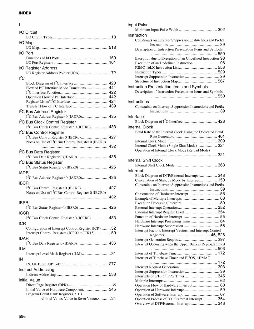
INDEX
I
I/O CircuitI/O Circuit Types ..................................................13
I/O MapI/O Map............................................................518
I/O PortFunctions of I/O Ports ..........................................160I/O Port Registers ...............................................161
I/O Register AddressI/O Register Address Pointer (IOA)...........................72
I2CBlock Diagram of I2C Interface ..............................423Flow of I2C Interface Mode Transitions ...................441I2C Interface Function..........................................422Operation Flow of I2C Interface .............................442Register List of I2C Interface .................................424Transfer Flow of I2C Interface ...............................439
I2C Bus Address RegisterI2C Bus Address Register 0 (IADR0).......................435
I2C Bus Clock Control RegisterI2C Bus Clock Control Register 0 (ICCR0) ...............433
I2C Bus Control RegisterI2C Bus Control Register 0 (IBCR0)........................427Notes on Use of I2C Bus Control Register 0 (IBCR0)
..........................................................432I2C Bus Data Register
I2C Bus Data Register 0 (IDAR0) ...........................436I2C Bus Status Register
I2C Bus Status Register 0 (IBSR0) ..........................425IADR
I2C Bus Address Register 0 (IADR0).......................435IBCR
I2C Bus Control Register 0 (IBCR0)........................427Notes on Use of I2C Bus Control Register 0 (IBCR0)
..........................................................432IBSR
I2C Bus Status Register 0 (IBSR0) ..........................425ICCR
I2C Bus Clock Control Register 0 (ICCR0) ...............433ICR
Configuration of Interrupt Control Register (ICR) ........52Interrupt Control Registers (ICR00 to ICR15)..............50
IDARI2C Bus Data Register 0 (IDAR0) ...........................436
ILMInterrupt Level Mask Register (ILM) .........................31
ININ, OUT, SETUP Token.......................................277
Indirect AddressingIndirect Addressing .............................................538
Initial ValueDirect Page Register (DPR)...............................................35Initial Value of Hardware Component......................345Program Count Bank Register (PCB)
<Initial Value: Value in Reset Vector>..........34
Input PulseMinimum Input Pulse Width ................................. 302
InstructionConstraints on Interrupt Suppression Instructions and Prefix
Instructions ............................................ 39Description of Instruction Presentation Items and Symbols
......................................................... 550Exception due to Execution of an Undefined Instruction 98Execution of an Undefined Instruction....................... 98F2MC-16LX Instruction List................................. 553Instruction Types................................................ 529Interrupt Suppression Instruction.............................. 39Structure of Instruction Map.................................. 567
Instruction Presentation Items and SymbolsDescription of Instruction Presentation Items and Symbols
......................................................... 550Instructions
Constraints on Interrupt Suppression Instructions and Prefix Instructions ............................................ 39
InterfaceBlock Diagram of I2C Interface ............................. 423
Internal ClockBaud Rate of the Internal Clock Using the Dedicated Baud
Rate Generator ...................................... 401Internal Clock Mode ........................................... 309Internal Clock Mode (Single Shot Mode) ................. 324Operation of Internal Clock Mode (Reload Mode)
......................................................... 321Internal Shift Clock
Internal Shift Clock Mode .................................... 368Interrupt
Block Diagram of DTP/External Interrupt ................ 348Cancellation of Standby Mode by Interrupt............... 150Constraints on Interrupt Suppression Instructions and Prefix
Instructions ............................................ 39Construction of Hardware Interrupt........................... 56Example of Multiple Interrupts ................................ 63Exception Processing Interrupt ................................ 80External Interrupt Operation.................................. 352External Interrupt Request Level ............................ 354Function of Hardware Interrupt................................ 55Hardware Interrupt Processing Time ......................... 64Hardware Interrupt Suppression ............................... 56Interrupt Factors, Interrupt Vectors, and Interrupt Control
Registers ....................................... 46, 526Interrupt Generation Request................................. 297Interrupt Occurring when the Upper Bank is Reprogrammed
......................................................... 503Interrupt of Timebase Timer.................................. 172Interrupt of Timebase Timer and EI2OS, µDMAC
......................................................... 172Interrupt Request Generation................................. 303Interrupt Suppression Instruction.............................. 39Interrupts of 8/16-bit PPG Timer ............................ 345Multiple Interrupts ................................................ 62Operation Flow of Hardware Interrupt ....................... 60Operation of Hardware Interrupt .............................. 59Operation of Software Interrupt ............................... 67Operation Process of DTP/External Interrupt ............ 354Overview of DTP/External Interrupt ....................... 348
596

INDEX
Precautions on Software Interrupt............................. 67Procedure for Using a Hardware Interrupt .................. 61Program Example of Interrupt Processing................. 101Receive Interrupt Generation and Flag Set Timing ..... 396Register List of DTP/External Interrupt ................... 349Return from Hardware Interrupt ............................... 58Return from Software Interrupt ................................ 66SOF Interrupt .................................................... 269Stack Operation at the Start of Interrupt Processing ...... 99Stack Operation when Interrupt Processing Returns
............................................................ 99Start of Hardware Interrupt ..................................... 58Start of Software Interrupt ...................................... 66Transition to Standby Mode and Interrupt................. 150Transmit Interrupt Generation and Flag Set Timing
.......................................................... 398Type and Function of Interrupt ................................ 42Type and Function of USB Interrupt ................. 47, 527UART Interrupt.................................................. 394
Interrupt Control RegisterConfiguration of Interrupt Control Register (ICR) ........ 52Interrupt Control Register Functions ................... 49, 53Interrupt Control Register List ................................. 48Interrupt Control Registers (ICR00 to ICR15) ............. 50Interrupt Factors, Interrupt Vectors, and Interrupt Control
Registers........................................ 46, 526Interrupt Factors
Interrupt Factors, Interrupt Vectors, and Interrupt Control Registers.............................................. 526
Interrupt Level Mask RegisterInterrupt Level Mask Register (ILM)......................... 31
Interrupt Suppression InstructionInterrupt Suppression Instruction.............................. 39Constraints on Interrupt Suppression Instructions and Prefix
Instructions ............................................ 39Interrupt Vector
Interrupt Factors, Interrupt Vectors, and Interrupt Control Registers.............................................. 526
Interrupt Vector.................................................... 45Interruption
Interruption Function of Extended I/O Serial Interface.......................................................... 373
Interruption of UART, EI2OS, and µDMAC ............. 395Notes on Use of Delay Interruption Generation Module
(Delay Interruption Request Latch) ............ 106Interval Timer
Interval Timer Function ....................................... 166Operation of Interval Timer Function (Timebase Timer)
.......................................................... 173IOA
I/O Register Address Pointer (IOA) .......................... 72ISCS
Extended Intelligent I/O Service (EI2OS) Status Register (ISCS)................................................... 73
ISDConfiguration of Extended Intelligent I/O Service (EI2OS)
Descriptor (ISD)...................................... 70
L
LatchNotes on Use of Delay Interruption Generation Module
(Delay Interruption Request Latch).............106Low-power Consumption
Block Diagram of Low-power Consumption Control Circuit..........................................................135
Low-power Consumption ModeOperation Status in Low-power Consumption Mode
..........................................................148Low-power Consumption Mode Control Register
Access to Low-power Consumption Mode Control Register..........................................................139
Low-power Consumption Mode Control Register (LPMCR)..........................................................137
LPMCRLow-power Consumption Mode Control Register (LPMCR)
..........................................................137LQFP-64
Package Dimension (LQFP-64) ..................................8
M
M1, M0Set Bit of Bus Mode (M1, M0) ...............................156
Machine ClockMachine Clock ...................................................127
Main Clock ModeMain Clock Mode, PLL Clock Mode .......................126
Master/Slave ModeMaster/Slave Mode Communication Function............414
Maximum CycleCount Clock and Maximum Cycle...........................298
MB90335 SeriesBlock Diagram of the MB90335 Series ........................7Feature of MB90335 Series .......................................2
MDSetting of Mode Pins (MD2 to MD0) .......................155
µDMACInterrupt of Timebase Timer and EI2OS, µDMAC
..........................................................172µDMAC Function .................................................82µDMAC Register List ............................................83µDMAC Use Procedure ..........................................97
MeasurementData of Measurement Result ..................................300Measurement Mode and Counter Operation...............301Operation Flow of Pulse Width Measurement ............304
Memory MapE2PROM Memory Map ........................................459Memory Map ...............................................21, 516System Configuration and E2PROM Memory Map
..........................................................458Memory Space
Arrangement of Multi Byte Length Data in Memory Space............................................................24
597

INDEX
Mini-HOSTFeature of USB Mini-HOST ..................................234Register of USB Mini-HOST.................................237Setting of Mini-HOST Function .............................261UART Block Diagram of USB Mini-HOST ..............236
MinimumMinimum Input Pulse Width..................................302
Minimum ConnectionExample of Minimum Connection to Flash Microcomputer
Programmer (when Using User Power)..........................................................513
Mode DataMode Data ........................................................156Relation between Mode Pin and Mode Data
(Recommended Example) ........................157Mode Data Read
State of Pins after Mode Data Read .........................117Mode Fetch
Mode Fetch .......................................................114Mode Pin
Mode Pin ..........................................................113Relation between Mode Pin and Mode Data
(Recommended Example) ........................157Setting of Mode Pins (MD2 to MD0).......................155
Mode SettingMode Setting .....................................................154
Mode TransitionsFlow of I2C Interface Mode Transitions ...................441
Multi Byte Length DataArrangement of Multi Byte Length Data in Memory Space
............................................................24Multi Byte Length Data Access ................................25
Multiple InterruptsMultiple Interrupts ................................................62Example of Multiple Interrupts ................................63
Multiplication RateSelection of PLL Clock Multiplication Rate ..............126
N
NCCFlag Change Suppression Prefix (NCC) .....................38
NoteNote.................................................................496Notes on Accessing the Low-Power Consumption Mode
Control Register (LPMCR) to Enter the Standby Mode ..................................................152
NULL TransferNULL Transfer Mode ..........................................232
O
ODRPort 4 Output Terminal Register (ODR4)..................164
One-shotOne-shot Operation Modes....................................297
One-to-one ModeBaud Rate of the External Clock (One-to-one Mode)
......................................................... 403Operating Mode
Operating Mode ......................................... 154, 342Operating State
Check Operating State ......................................... 296Setting and Operating State................................... 460
OperationEach Register Operation when Write Command Responds
......................................................... 225Operation of USB Function................................... 219
Operation ModeCounter Operation Mode ...................................... 310CPU Intermittent Operation Mode .......................... 133One-shot Operation Modes ................................... 297Operation in Synchronous Mode (Operation Mode 2)
......................................................... 409Reload Operation Mode ....................................... 297Selects Operation Mode ....................................... 294CPU Operation Modes and Current Consumption
......................................................... 132Oscillation Clock Frequency
Oscillation Clock Frequency and Serial Clock Input Frequency............................................ 508
Oscillation Stabilization Wait TimeOscillation Stabilization Wait Time ................ 128, 151Oscillation Stabilization Wait Time Function ............ 173Reset Factors and Oscillation Stabilization Wait Times
......................................................... 110Oscillation Stabilization Waiting
Oscillation Stabilization Waiting Reset State............. 111Oscillator
Connection of Oscillator and External Clock............. 129Others
The Others ........................................................ 438OUT
IN, OUT, SETUP Token ...................................... 277
P
Package DimensionPackage Dimension (LQFP-64) ................................. 8
PacketData Packet ....................................................... 266Handshake Packet............................................... 267Packet End Timing ............................................. 272Setting of Token Packet ....................................... 264
Packet TransferPacket Transfer Mode.......................................... 228
PACSRAddress Detection Control Register (PACSR) ........... 453
PADRDetect Address Setting Registers (PADR0, PADR1)
......................................................... 455Patch Processing
Flow of Patch Processing ..................................... 462
598

INDEX
Patch ProgramOperation of Address Match Detection Function at Storing
Patch Program in E2PROM ...................... 461PC
Program Counter (PC) ........................................... 33PCB
Program Count Bank Register (PCB) ............................... 34
PDRPort Data Register (PDR0 to PDR2, PDR4 to PDR6)
.......................................................... 162Peripheral Equipment
Condition of Peripheral Equipment Connected Outside.......................................................... 354
Physical AddressRelation between Access Area and Physical Address
.......................................................... 157Pin Assignment
Pin Assignment (FPT-64P-M09) ................................ 9Pin Function
Pin Function ........................................................ 10Pin Output
Pin Output Control of Pulse .................................. 344PLL Clock
Selection of PLL Clock Multiplication Rate .............. 126PLL Clock Mode
Main Clock Mode, PLL Clock Mode....................... 126Pointer
Buffer Address Pointer (BAP) ................................. 74DMA Buffer Address Pointer (DBAPH/DBAPM/DBAPL)
............................................................ 95DMA I/O Register Address Pointer (DIOAH/DIOAL)
............................................................ 92Port 4 Output Terminal Register
Port 4 Output Terminal Register (ODR4) ................. 164Port Data Register
Port Data Register (PDR0 to PDR2, PDR4 to PDR6).......................................................... 162
Port Direction RegisterPort Direction Register (DDR0 to DDR2, DDR4 to DDR6)
.......................................................... 163Port0, 1 Pull-up Resistance Register
Port0, 1 Pull-up Resistance Register (RDR0,RDR1).......................................................... 164
PowerConnection Example in Single-chip Mode
(when Using User Power) ........................ 511Example of Minimum Connection to Flash Microcomputer
Programmer (when Using User Power).......................................................... 513
PPGPPG Output Operation ......................................... 343PPG0 to PPG3 Output Control Register (PPG01/PPG23)
.......................................................... 339PPG Reload Registers
PPG Reload Registers (PRLL0 to PRLL3, PRLH0 to PRLH3)............................................... 341
PPG TimerBlock Diagram of 8/16-bit PPG Timer .....................331Interrupts of 8/16-bit PPG Timer.............................345Outline of Operation of 8/16-bit PPG Timer ..............342Overview of 8/16-bit Timer PPG Timer....................330Register List of 8/16-bit PPG Timer.........................333
PPG0 to PPG3 Output Control RegisterPPG0 to PPG3 Output Control Register (PPG01/PPG23)
..........................................................339PPG0/2 Operation Mode Control Register
PPG0/2 Operation Mode Control Register (PPGC0/PPGC2)..........................................................334
PPG1/PPG3 Operation Mode Control RegisterPPG1/PPG3 Operation Mode Control Register
(PPGC1/PPGC3)....................................336PPGC
PPG0/2 Operation Mode Control Register (PPGC0/PPGC2)..........................................................334
PPG1/PPG3 Operation Mode Control Register (PPGC1/PPGC3)....................................336
PrefixBank Select Prefix .................................................37Common Register Bank Prefix (CMR) .......................38Flag Change Suppression Prefix (NCC)......................38
Prefix CodeArray of Prefix Code..............................................40
Prefix InstructionsConstraints on Interrupt Suppression Instructions and Prefix
Instructions .............................................39Priority
Priority Level of STP, SLP, and TMD Bit .................139PRLL
PPG Reload Registers (PRLL0 to PRLL3, PRLH0 to PRLH3) ...............................................341
Processing TimeExtended Intelligent I/O Service (EI2OS) Processing Time
(Time for One Transfer).............................77Hardware Interrupt Processing Time ..........................64
Processor StatusProcessor Status (PS) .............................................30
ProductProduct Lineup .......................................................5
ProgramOperation of Address Match Detection Function at Storing
Patch Program in E2PROM ......................461Program Execution ..............................................457
Program Count Bank RegisterProgram Count Bank Register (PCB)................................34
Program CounterProgram Counter (PC) ............................................33
Program ExampleProgram Example for Address Match Detection Function
..........................................................463Program Example of Interrupt Processing .................101Program Example of Timebase Timer ......................177Program Examples of Watchdog Timer ....................187
599
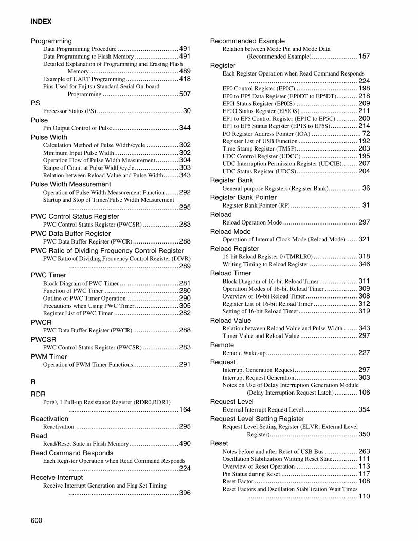
INDEX
ProgrammingData Programming Procedure ................................491Data Programming to Flash Memory .......................491Detailed Explanation of Programming and Erasing Flash
Memory...............................................489Example of UART Programming............................418Pins Used for Fujitsu Standard Serial On-board
Programming ........................................507PS
Processor Status (PS) .............................................30Pulse
Pin Output Control of Pulse...................................344Pulse Width
Calculation Method of Pulse Width/cycle .................302Minimum Input Pulse Width..................................302Operation Flow of Pulse Width Measurement............304Range of Count at Pulse Width/cycle.......................303Relation between Reload Value and Pulse Width........343
Pulse Width MeasurementOperation of Pulse Width Measurement Function .......292Startup and Stop of Timer/Pulse Width Measurement
..........................................................295PWC Control Status Register
PWC Control Status Register (PWCSR) ...................283PWC Data Buffer Register
PWC Data Buffer Register (PWCR) ........................288PWC Ratio of Dividing Frequency Control Register
PWC Ratio of Dividing Frequency Control Register (DIVR)..........................................................289
PWC TimerBlock Diagram of PWC Timer ...............................281Function of PWC Timer .......................................280Outline of PWC Timer Operation ...........................290Precautions when Using PWC Timer .......................305Register List of PWC Timer ..................................282
PWCRPWC Data Buffer Register (PWCR) ........................288
PWCSRPWC Control Status Register (PWCSR) ...................283
PWM TimerOperation of PWM Timer Functions........................291
R
RDRPort0, 1 Pull-up Resistance Register (RDR0,RDR1)
..........................................................164Reactivation
Reactivation ......................................................295Read
Read/Reset State in Flash Memory..........................490Read Command Responds
Each Register Operation when Read Command Responds..........................................................224
Receive InterruptReceive Interrupt Generation and Flag Set Timing
..........................................................396
Recommended ExampleRelation between Mode Pin and Mode Data
(Recommended Example)........................ 157Register
Each Register Operation when Read Command Responds......................................................... 224
EP0 Control Register (EP0C) ................................ 198EP0 to EP5 Data Register (EP0DT to EP5DT)........... 218EP0I Status Register (EP0IS) ................................ 209EP0O Status Register (EP0OS) .............................. 211EP1 to EP5 Control Register (EP1C to EP5C) ........... 200EP1 to EP5 Status Register (EP1S to EP5S).............. 214I/O Register Address Pointer (IOA) .......................... 72Register List of USB Function ............................... 192Time Stamp Register (TMSP)................................ 203UDC Control Register (UDCC) ............................. 195UDC Interruption Permission Register (UDCIE)........ 207UDC Status Register (UDCS)................................ 204
Register BankGeneral-purpose Registers (Register Bank)................. 36
Register Bank PointerRegister Bank Pointer (RP) ..................................... 31
ReloadReload Operation Mode ....................................... 297
Reload ModeOperation of Internal Clock Mode (Reload Mode)...... 321
Reload Register16-bit Reload Register 0 (TMRLR0) ....................... 318Writing Timing to Reload Register ......................... 346
Reload TimerBlock Diagram of 16-bit Reload Timer .................... 311Operation Modes of 16-bit Reload Timer ................. 309Overview of 16-bit Reload Timer ........................... 308Register List of 16-bit Reload Timer ....................... 312Setting of 16-bit Reload Timer............................... 319
Reload ValueRelation between Reload Value and Pulse Width ....... 343Timer Value and Reload Value .............................. 297
RemoteRemote Wake-up................................................ 227
RequestInterrupt Generation Request................................. 297Interrupt Request Generation................................. 303Notes on Use of Delay Interruption Generation Module
(Delay Interruption Request Latch) ............ 106Request Level
External Interrupt Request Level ............................ 354Request Level Setting Register
Request Level Setting Register (ELVR: External Level Register).............................................. 350
ResetNotes before and after Reset of USB Bus ................. 263Oscillation Stabilization Waiting Reset State............. 111Overview of Reset Operation ................................ 113Pin Status during Reset ........................................ 117Reset Factor ...................................................... 108Reset Factors and Oscillation Stabilization Wait Times
......................................................... 110
600

INDEX
Reset FactorCorrespondence of Reset Factor Bit and Reset Factor
.......................................................... 116Notes on Reset Factor Bit ..................................... 116Reset Factor Bit ................................................. 115
Reset StateRead/Reset State in Flash Memory ......................... 490
Reset ValuesList of Registers and Reset Values of Address Match
Detection Function................................. 452List of Registers and Reset Values of Flash Memory
.......................................................... 467Reset Vector
Hardwired Reset Vector Addresses ......................... 479Program Count Bank Register (PCB)
<Initial Value: Value in Reset Vector> ......... 34Resume
Resume Operation .............................................. 273Retry
Retry Function ................................................... 268Retry Timer Setting Register
Retry Timer Setting Register (HRTIMER)................ 254Return
Return from Hardware Interrupt ............................... 58ROM Mirror Function Select Module
Block Diagram of ROM Mirror Function Select Module.......................................................... 446
ROM Mirror Function Select RegisterROM Mirror Function Select Register (ROMM) ........ 447
ROM Mirror Function Selection ModuleRegister of ROM Mirror Function Selection Module
.......................................................... 446ROMM
ROM Mirror Function Select Register (ROMM) ........ 447RP
Register Bank Pointer (RP) ..................................... 31
S
SCRSerial Control Register 0,1 (SCR0,SCR1)................. 383
SDCRCommunication Prescaler Control Register (SDCR)
.......................................................... 365SDR
Serial Data Register (SDR) ................................... 364Sector
Erasing Procedure for Flash Memory Sectors ............ 494Note on Sector Erasing ........................................ 494Sector and Bank Configuration of 512 Kbit Flash Memory
.......................................................... 467Sector Erase Suspension....................................... 496
Sector Erase TimerSector Erase Timer Flag (DQ3).............................. 486
Sector ErasingErasing Any Data in Flash Memory (Sector Erasing)
.......................................................... 494
Sector Switching RegisterSector Switching Register (SSR0) ...........................501Sector Switching Register (SSR0) Setting Procedure
..........................................................503SEN
SEN0 Bit access Sector Map..................................502Serial
List of Register in Extended I/O Serial Interface .........359Operation during Transfer Serial Data ......................372
Serial ClockOscillation Clock Frequency and Serial Clock Input
Frequency.............................................508Serial Control Register
Serial Control Register 0,1 (SCR0,SCR1) .................383Serial Data Register
Serial Data Register (SDR) ....................................364Serial I/O
Operation State of Serial I/O ..................................369Serial Input Data Register
Serial Input Data Register 0,1 (SIDR0,SIDR1) ...........390Serial Interface
Block Diagram in Extended I/O Serial Interface .........358Interruption Function of Extended I/O Serial Interface
..........................................................373Outline of Extended I/O Serial Interface ...................358Outline of Operation of Extended I/O Serial Interface
..........................................................367Serial Mode Control Status Register
Serial Mode Control Status Register (SMCS).............360Serial Mode Register
Serial Mode Register 0,1 (SMR0,SMR1) ..................385Serial On-Board
The Serial On-Board Writing Basic Component .........506Serial On-board
Pins Used for Fujitsu Standard Serial On-board Programming ........................................507
Serial Output Data RegisterSerial Output Data Register 0,1 (SODR0,SODR1)
..........................................................391Serial Status Register
Serial Status Register 0,1 (SSR0,SSR1) ....................387Serial Writing
Example of Connecting Serial Writing .....................510Setting
Setting and Operating State ...................................460SETUP
IN, OUT, SETUP Token .......................................277Shift Operation
Start/stop Timing of Shift Operation and Timing of I/O..........................................................371
SIDRSerial Input Data Register 0,1 (SIDR0,SIDR1) ...........390
Single MeasurementSingle Measurement and Continuous Measurement
..........................................................300
601

INDEX
Single Shot ModeInternal Clock Mode (Single Shot Mode)..................324
Single-chip ModeConnection Example in Single-chip Mode
(when Using User Power) ........................511Pin State in Single-chip Mode ................................149
Sleep ModeCancellation of Sleep Modes .................................143Transition to Sleep Mode ......................................142
SLPPriority Level of STP, SLP, and TMD Bit.................139
SMCSSerial Mode Control Status Register (SMCS) ............360
SMRSerial Mode Register 0,1 (SMR0,SMR1)..................385
SODRSerial Output Data Register 0,1 (SODR0,SODR1)
..........................................................391SOF
SOF Interrupt.....................................................269SOF Token ........................................................278
SOF Interruption FRAME Comparison RegisterSOF Interruption FRAME Comparison Register (HFCOMP)
..........................................................253Software Interrupt
Operation of Software Interrupt................................67Precautions on Software interrupt .............................67Return from Software Interrupt ................................66Start of Software Interrupt.......................................66
SSPUser Stack Pointer (USP) and System Stack Pointer (SSP)
............................................................29SSR
Sector Switching Register (SSR0)...........................501Sector Switching Register (SSR0) Setting Procedure
..........................................................503Serial Status Register 0,1 (SSR0,SSR1)....................387
Stack AreaStack Area.........................................................100
Stack OperationStack Operation at the Start of Interrupt Processing.......99Stack Operation when Interrupt Processing Returns
............................................................99Standby Mode
Cancellation of Standby Mode by Interrupt ...............150Operation Status in Standby Mode ..........................141Standby Mode ....................................................133Transition to Standby Mode and Interrupt .................150
StartStart/stop Timing of Shift Operation and Timing of I/O
..........................................................371Start Condition
Start Condition ...................................................437Startup
Operation after Startup .........................................295State
Read/Reset State in Flash Memory..........................490
State TransitionState Transition Diagram...................................... 147State Transition of Counter Operation ..................... 320
Status RegisterExtended Intelligent I/O Service (EI2OS) Status Register
(ISCS) .................................................. 73Stop Condition
Stop Condition................................................... 437Stop Mode
Transition to Stop Mode....................................... 145Cancellation of Stop Modes .................................. 145
Stop TimingStart/stop Timing of Shift Operation and Timing of I/O
......................................................... 371Stops
Stops ............................................................... 296STP
Priority Level of STP, SLP, and TMD Bit ................ 139Structure
Structure of Instruction Map.................................. 567Suspend
Suspend Operation.............................................. 273Suspend Processing............................................. 226
Synchronous ModeOperation in Synchronous Mode (Operation Mode 2)
......................................................... 409System Configuration
System Configuration and E2PROM Memory Map......................................................... 458
System Stack PointerUser Stack Pointer (USP) and System Stack Pointer (SSP)
........................................................... 29
T
TBTCTimebase Timer Control Register (TBTC)................ 170
Time Stamp RegisterTime Stamp Register (TMSP)................................ 203
Timebase TimerBlock Diagram of Timebase Timer ......................... 168Interrupt of Timebase Timer.................................. 172Interrupt of Timebase Timer and EI2OS, µDMAC
......................................................... 172Operation of Interval Timer Function (Timebase Timer)
......................................................... 173Operations of Timebase Timer............................... 176Precautions when Using Timebase Timer ................. 175Program Example of Timebase Timer ..................... 177
Timebase Timer Control RegisterTimebase Timer Control Register (TBTC)................ 170
Timebase Timer ModeTransition to Timebase Timer Mode ....................... 144Cancellation of Timebase Timer Modes ................... 144
TimerClearing Timer................................................... 297Operation Flow of Timer ...................................... 299
602

INDEX
Startup and Stop of Timer/Pulse Width Measurement.......................................................... 295
Timer Control Status RegisterTimer Control Status Register 0 (TMCSR0).............. 313
Timer CycleTimer Cycle ...................................................... 298
Timer Register16-bit Timer Register 0 (TMR0) ............................ 317
Timer ValueTimer Value and Reload Value .............................. 297
TimingStart/stop Timing of Shift Operation and Timing of I/O
.......................................................... 371Timing Limit Over
Timing Limit Over Flag (DQ5) .............................. 485TMCSR
Timer Control Status Register 0 (TMCSR0).............. 313TMD
Priority Level of STP, SLP, and TMD Bit ................ 139TMR
16-bit Timer Register 0 (TMR0) ............................ 31716-bit Timer Register 0 (TMR0)/16-bit Reload Register 0
(TMRLR0)........................................... 317TMRLR
16-bit Reload Register 0 (TMRLR0) ....................... 31816-bit Timer Register 0 (TMR0)/16-bit Reload Register 0
(TMRLR0)........................................... 317TMSP
Time Stamp Register (TMSP)................................ 203Toggle Bit Flag
Toggle Bit Flag (DQ6)......................................... 484Toggle Bit Flag (DQ2)......................................... 487
TokenIN, OUT, SETUP Token ...................................... 277SOF Token........................................................ 278
Token PacketSetting of Token Packet ....................................... 264
TransferData Number Automatic Transfer Mode .................. 230Extended Intelligent I/O Service (EI2OS) Processing Time
(Time for One Transfer) ............................ 77NULL Transfer Mode .......................................... 232Packet Transfer Mode.......................................... 228
Transfer FlowTransfer Flow of I2C Interface ............................... 439
Transfer Serial DataOperation during Transfer Serial Data ..................... 372
Transfer SpeedAcquiring Transfer Speed of Destination USB Device and
Selecting Clock ..................................... 261Transmit Interrupt
Transmit Interrupt Generation and Flag Set Timing .... 398Type
Type and Function of USB Interrupt ......................... 47
U
UARTExample of UART Programming ............................418Interruption of UART, EI2OS, and µDMAC ..............395List of UART Register .........................................382Notes on Using UART .........................................417Operation of UART .............................................404UART Baud Rate Selection ...................................400UART Block Diagram..........................................378UART Block Diagram of USB Mini-HOST ..............236UART EI2OS Function.........................................395UART Function ..................................................376UART Interrupt ..................................................394UART Pins ........................................................381UART Prescaler Control Register 0, 1 (UTCR0, UTCR1)
and UART Prescaler Reload Register 0, 1 (UTRLR0, UTRLR1) ..............................392
UART Prescaler Control RegisterUART Prescaler Control Register 0, 1 (UTCR0, UTCR1)
and UART Prescaler Reload Register 0, 1 (UTRLR0, UTRLR1) ..............................392
UART Prescaler Reload RegisterUART Prescaler Control Register 0, 1 (UTCR0, UTCR1)
and UART Prescaler Reload Register 0, 1 (UTRLR0, UTRLR1) ..............................392
UDC Control RegisterUDC Control Register (UDCC) ..............................195
UDC Interruption Permission RegisterUDC Interruption Permission Register (UDCIE) ........207
UDC Status RegisterUDC Status Register (UDCS) ................................204
UDCCUDC Control Register (UDCC) ..............................195
UDCIEUDC Interruption Permission Register (UDCIE) ........207
UDCSUDC Status Register (UDCS) ................................204
Undefined InstructionException due to Execution of an Undefined Instruction
............................................................98Execution of an Undefined Instruction .......................98
Upper BankInterrupt Occurring when the Upper Bank is Reprogrammed
..........................................................503USB
Block Diagram of USB Function ............................191Connected Detection of External USB Device............261Disconnection Status, Connection Status of the External
USB Device ..........................................261Features of USB Function .....................................190Notes before and after Reset of USB Bus ..................263Operation of USB Function ...................................219Register List of USB Function................................192Type and Function of USB Interrupt ..........................47
USB BusNotes before and after Reset of USB Bus ..................263
603

INDEX
USB DeviceAcquiring Transfer Speed of Destination USB Device and
Selecting Clock .....................................261USB Host
Diversity with USB Host ......................................235USB Interrupt
Type and Function of USB Interrupt........................527USB Mini-HOST
Feature of USB Mini-HOST ..................................234Register of USB Mini-HOST.................................237UART Block Diagram of USB Mini-HOST ..............236
USB System ConnectionExample USB System Connection ..........................222
User PowerConnection Example in Single-chip Mode
(when Using User Power) ........................511Example of Minimum Connection to Flash Microcomputer
Programmer (when Using User Power)..........................................................513
User Stack PointerUser Stack Pointer (USP) and System Stack Pointer (SSP)
............................................................29USP
User Stack Pointer (USP) and System Stack Pointer (SSP)............................................................29
UTCRUART Prescaler Control Register 0, 1 (UTCR0, UTCR1)
and UART Prescaler Reload Register 0, 1 (UTRLR0, UTRLR1)..............................392
UTRLRUART Prescaler Control Register 0, 1 (UTCR0, UTCR1)
and UART Prescaler Reload Register 0, 1 (UTRLR0, UTRLR1) ............................. 392
V
VectorsInterrupt Factors, Interrupt Vectors, and Interrupt Control
Registers ............................................... 46
W
Wake-upRemote Wake-up................................................ 227Wake-up from Host............................................. 227
Watchdog TimerBlock Diagram of Watchdog Timer ........................ 183Functions of Watchdog Timer ............................... 180Operations of Watchdog Timer .............................. 184Precautions when Using Watchdog Timer ................ 186Program Examples of Watchdog Timer ................... 187
Watchdog Timer Control RegisterWatchdog Timer Control Register (WDTC).............. 181
WDTCWatchdog Timer Control Register (WDTC).............. 181
WriteOperation during Write/Erase ................................ 504
Write Command RespondsEach Register Operation when Write Command Responds
......................................................... 225
604

CM44-10137-3E
FUJITSU SEMICONDUCTOR • CONTROLLER MANUAL
F2MC-16LX
16-BIT MICROCONTROLLER
MB90335 Series
HARDWARE MANUAL
August 2006 the third edition
Published FUJITSU LIMITED Electronic Devices
Edited Business Promotion Dept.
