1633 nanorobotics 46. nanorobotics
TRANSCRIPT

1633
Nanorobotics46. Nanorobotics
Bradley J. Nelson, Lixin Dong
Nanorobotics is the study of robotics at thenanometer scale, and includes robots that arenanoscale in size and large robots capable of ma-nipulating objects that have dimensions in thenanoscale range with nanometer resolution. Withthe ability to position and orient nanometer-scaleobjects, nanorobotic manipulation is a promis-ing way to enable the assembly of nanosystemsincluding nanorobots.
This chapter overviews the state of the artof nanorobotics, outlines nanoactuation, andfocuses on nanorobotic manipulation systems andtheir application in nanoassembly, biotechnologyand the construction and characterization ofnanoelectromechanical systems (NEMS) througha hybrid approach.
Because of their exceptional properties andunique structures, carbon nanotubes (CNTs) andSiGe/Si nanocoils are used to show basic processesof nanorobotic manipulation, structuring andassembly, and for the fabrication of NEMS includingnano tools, sensors and actuators.
A series of processes of nanorobotic ma-nipulation, structuring and assembly has beendemonstrated experimentally. Manipulation of in-dividual CNTs in 3-D free space has been shownby grasping using dielectrophoresis and plac-ing with both position and orientation controlfor mechanical and electrical property charac-terization and assembly of nanostructures anddevices. A variety of material property investi-gations can be performed, including bending,buckling, and pulling to investigate elasticity aswell as strength and tribological characterization.Structuring of CNTs can be performed includ-ing shape modification, the exposure of nestedcores, and connecting CNTs by van der Waalsforces, electron-beam-induced deposition andmechanochemical bonding.
46.1 Overview of Nanorobotics ...................... 1634
46.2 Actuation at Nanoscales ........................ 163546.2.1 Electrostatics ............................. 163646.2.2 Electromagnetics ........................ 163646.2.3 Piezoelectrics ............................. 163646.2.4 Other Techniques ....................... 1637
46.3 Nanorobotic Manipulation Systems ........ 163746.3.1 Overview ................................... 163746.3.2 Nanorobotic Manipulation
Systems .................................... 1641
46.4 Nanorobotic Assembly ........................... 164246.4.1 Overview ................................... 164246.4.2 Carbon Nanotubes ...................... 164446.4.3 Nanocoils .................................. 1648
46.5 Applications ......................................... 165146.5.1 Robotic Biomanipulation ............ 165146.5.2 Nanorobotic Devices ................... 1652
References .................................................. 1654
Nanorobotics provides novel techniques forexploring the biodomain by manipulation andcharacterization of nanoscale objects such as cel-lular membranes, DNA and other biomolecules.Nano tools, sensors and actuators can providemeasurements and/or movements that are cal-culated in nanometers, gigahertz, piconewtons,femtograms, etc., and are promising for molecularmachines and bio- and nanorobotics applications.Efforts are focused on developing enabling tech-nologies for nanotubes and other nanomaterialsand structures for NEMS and nanorobotics. By com-bining bottom-up nanorobotic manipulation andtop-down nanofabrication processes, a hybrid ap-proach is demonstrated for creating complex 3-Dnanodevices. Nanomaterial science, bionanotech-nology, and nanoelectronics will benefit fromadvances in nanorobotics.
PartG
46

1634 Part G Industrial Applications
46.1 Overview of Nanorobotics
Progress in robotics over the past years has dramati-cally extended our ability to explore the world fromperception, cognition and manipulation perspectives ata variety of scales extending from the edges of the solarsystem down to individual atoms (Fig. 46.1). At the bot-tom of this scale, technology has been moving towardgreater control of the structure of matter, suggestingthe feasibility of achieving thorough control of the mo-lecular structure of matter atom by atom as RichardFeynman first proposed in 1959 in his prophetic articleon miniaturization [46.1]:
What I want to talk about is the problem of manip-ulating and controlling things on a small scale. . . Iam not afraid to consider the final question as towhether, ultimately – in the great future – we canarrange the atoms the way we want: the very atoms,all the way down!
He asserted that:
At the atomic level, we have new kinds of forcesand new kinds of possibilities, new kinds of effects.The problems of manufacture and reproduction ofmaterials will be quite different. The principles of
Neareststars
Edge of thesolar system
Eathto mars
1015
1012
109
106
103
10–910–6
10–3
Ånm
µm
mm
m
km
Assembler
1
Fig. 46.1 Robotic exploration
physics, as far as I can see, do not speak against thepossibility of maneuvering things atom by atom.
This technology is now labeled nanotechnology.The great future of Feynman began to be realized in
the 1980s. Some of the capabilities he dreamed of havebeen demonstrated, while others are being developed.Nanorobotics represents the next stage in miniaturiza-tion for maneuvering nanoscale objects. Nanoroboticsis the study of robotics at the nanometer scale, and in-cludes robots that are nanoscale in size, i. e., nanorobots,and large robots capable of manipulating objects thathave dimensions in the nanoscale range with nanome-ter resolution, i. e., nanorobotic manipulators. Thefield of nanorobotics brings together several disci-plines, including nanofabrication processes used forproducing nanoscale robots, nanoactuators, nanosen-sors, and physical modeling at nanoscales. Nanoroboticmanipulation technologies, including the assembly ofnanometer-sized parts, the manipulation of biologicalcells or molecules, and the types of robots used to per-form these types of tasks also form a component ofnanorobotics.
As the 21st century unfolds, the impact of nanotech-nology on the health, wealth, and security of humankind
PartG
46.1

Nanorobotics 46.2 Actuation at Nanoscales 1635
is expected to be at least as significant as the combinedinfluences in the 20th century of antibiotics, the inte-grated circuit, and human-made polymers. For example,Lane stated in 1998 [46.2]:
If I were asked for an area of science and engineer-ing that will most likely produce the breakthroughsof tomorrow, I would point to nanoscale science andengineering.
The great scientific and technological opportunitiesnanotechnology presents have stimulated extensive ex-ploration of the nanoworld and initiated an excitingworldwide competition, which has been accelerated bythe publication of the National Nanotechnology Initia-tive by the US government in 2000 [46.3]. Nanoroboticswill play a significant role as an enabling nano-technology and could ultimately be a core part ofnanotechnology if Drexler’s machine-phase nanosys-tems based on self-replicative molecular assemblers viamechanosynthesis can be realized [46.4].
By the early 1980s, scanning tunneling microscopes(STMs) [46.5] radically changed the ways in whichwe interacted with and even regarded single atoms andmolecules. The very nature of proximal probe methodsencourages exploration of the nanoworld beyond con-ventional microscopic imaging. Scanned probes nowallow us to perform engineering operations on singlemolecules, atoms, and bonds, thereby providing a toolthat operates at the ultimate limits of fabrication. Theyhave also enabled exploration of molecular propertieson an individual nonstatistical basis.
STMs and other nanomanipulators are nonmolec-ular machines but use bottom-up strategies. Althoughperforming only one molecular reaction at a time isobviously impractical for making large amounts ofa product, it is a promising way to provide the nextgeneration of nanomanipulators. Most importantly, it ispossible to realize the directed assembly of molecules orsupermolecules to build larger nanostructures throughnanomanipulation. The products produced by nanoma-
nipulation could be the first step of a bottom-up strategyin which these assembled products are used to self-assemble into nanomachines.
One of the most important applications of nano-robotic manipulation will be nanorobotic assembly.However, it appears that until assemblers capable ofreplication can be built, the parallelism of chemicalsynthesis and self-assembly are necessary when start-ing from atoms; groups of molecules can self-assemblequickly due to their thermal motion, enabling them toexplore their environments and find (and bind to) com-plementary molecules. Given their key role in naturalmolecular machines, proteins are obvious candidatesfor early work in self-assembling artificial molecularsystems. Degrado [46.6] demonstrated the feasibil-ity of designing protein chains that predictably foldinto solid molecular objects. Progress is also beingmade in artificial enzymes and other relatively smallmolecules that perform functions like those of natu-ral proteins; the 1987 Nobel prize for chemistry wentto Cram and Lehn for such work on supramolecularchemistry [46.7]. Several bottom-up strategies usingself-assembly appear feasible [46.8]. Fujita et al.’s pi-oneering work has shown that self-assembly can bedirected by adroitly exploiting the chemical and elec-trical bonds that hold natural molecules together, andhence get molecules to form desired nanometer-scalestructures [46.9]. Chemical synthesis, self assembly,and supramolecular chemistry make it possible to pro-vide building blocks at relatively large sizes beginningfrom the nanometer scale. Nanorobotic manipulationserves as the base for a hybrid approach to constructnanodevices by structuring these materials to obtainbuilding blocks and assembling them into more com-plex systems.
This chapter focuses on nanorobotics including ac-tuation, manipulation and assembly at the nanoscale.The main goal of nanorobotics is to provide an effec-tive technology for the experimental exploration of thenanoworld, and to push the boundaries of this explo-ration from a robotics research perspective.
46.2 Actuation at Nanoscales
The positioning of nanorobots and nanorobotic ma-nipulators depends largely on nanoactuators. Whilenanosized actuators for nanorobots are still underexploration and relatively far from implementation, mi-croelectromechanical system (MEMS)-based efforts are
focused on shrinking their sizes [46.10]. Nanometer-resolution motion has been extensively investigatedand can be generated using various actuation prin-ciples. Electrostatics, electromagnetics, and piezo-electrics are the most common ways to realize actuation
PartG
46.2

1636 Part G Industrial Applications
Table 46.1 Actuation with MEMS
Actuation Type of Volume Speed Force Stroke Resolution Power density Ref.
principle motion (mm3) (s−1) (N) (m) (m) (W/m3)
Electrostatic Linear 400 5000 1 × 10⁻⁷ 6 × 10⁻⁶ n/a 200 [46.12]
Magnetic Linear 0.4 × 0.4 × 0.5 1000 2.6 × 10⁻⁶ 1 × 10⁻⁴ n/a 3000 [46.13]
Piezoelectric Linear 25.4 × 12.7 × 1.6 4000 350 1 × 10⁻³ 7 × 10⁻⁸ n/a [46.14]
Actuation Type of Volume Speed Torque Stroke Resolution Power density Ref.
principle motion (mm3) (rad/s) (N m) (rad) (rad) (W/m3)
Electrostatic Rotational π/4 × 0.52 × 3 40 2 × 10⁻⁷ 2π n/a 900 [46.15]
Magnetic Rotational 2 × 3.7 × 0.5 150 1 × 10⁻⁶ 2π 5/36π 3000 [46.16]
Piezoelectric Rotational π/4 × 1.52 × 0.5 30 2 × 10⁻¹¹ 0.7 n/a n/a [46.17]
at nanoscales. For nanorobotic manipulation, besidesnanoresolution and compact sizes, actuators generatinglarge strokes and high forces are best suited for such ap-plications. The speed criteria are of less importance aslong as the actuation speed is in the range of a coupleof hertz and above. Table 46.1 provides a small selec-tion of early works on actuators [46.11–16] suitablein actuation principle actuators suitable for nanoroboticapplications (partially adapted from [46.10]).
Several extensive reviews on various actuation prin-ciples have been published [46.17–21]. During thedesign of an actuator, the tradeoffs among rangeof motion, force, speed (actuation frequency), powerconsumption, control accuracy, system reliability, ro-bustness, load capacity, etc. must be taken into consider-ation. This section reviews basic actuation technologiesand potential applications at nanometer scales.
46.2.1 Electrostatics
Electrostatic charge arises from a build up or deficit offree electrons in a material, which can exert an attrac-tive force on oppositely charged objects, or a repulsiveforce on similarly charged objects. Since electrostaticfields arise and disappear rapidly, such devices will like-wise demonstrate very fast operation speeds and be littleaffected by ambient temperatures.
Recent investigations have produced many exam-ples of miniature devices using electrostatic force foractuation including silicon micro motors [46.22, 23],microvalves [46.24], and microtweezers [46.25]. Thistype of actuation is important for achieving nanosizedactuation.
Electrostatic fields can exert great forces, but gener-ally across very short distances. When the electric fieldmust act over larger distances, a higher voltage willbe required to maintain a given force. The extremely
low-current consumption associated with electrostaticdevices makes for highly efficient actuation.
46.2.2 Electromagnetics
Electromagnetism arises from electric current movingthrough a conducting material. Attractive or repulsiveforces are generated adjacent to the conductor and pro-portional to the current flow. Structures can be builtwhich gather and focus electromagnetic forces, and har-ness these forces to create motion.
Electromagnetic fields arise and disappear rapidly,thus permitting devices with very fast operation speeds.Since electromagnetic fields can exist over a wide rangeof temperatures, performance is primarily limited bythe properties of the materials used in constructing theactuator.
One example of a microfabricated electromagneticactuator is a microvalve which uses a small electro-magnetic coil wrapped around a silicon micromachinedvalve structure [46.26]. However, the downward scala-bility of electromagnetic actuators into the micro- andnanorealm may be limited by the difficulty of fabri-cating small electromagnetic coils. Furthermore, mostelectromagnetic devices require perpendicularity be-tween the current conductor and the moving element,presenting a difficulty for planar fabrication techniquescommonly used to make silicon devices.
An important advantage of electromagnetic devicesis their high efficiency in converting electrical energyinto mechanical work. This translates into less currentconsumption from the power source.
46.2.3 Piezoelectrics
Piezoelectric motion arises from the dimensionalchanges generated in certain crystalline materials when
PartG
46.2
Nanorobotics 46.3 Nanorobotic Manipulation Systems 1637
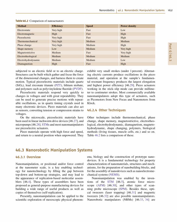
Table 46.2 Comparison of nanoactuators
Method Efficiency Speed Power density
Electrostatic Very high Fast Low
Electromagnetic High Fast High
Piezoelectric Very high Fast High
Thermomechanical Very high Medium Medium
Phase change Very high Medium High
Shape memory Low Medium Very high
Magnetostrictive Medium Fast Very high
Electrorheological Medium Medium Medium
Electrohydrodynamic Medium Medium Low
Diamagnetism High Fast High
subjected to an electric field or to an electric charge.Structures can be built which gather and focus the forceof the dimensional changes, and harness them to createmotion. Typical piezoelectric materials include quartz(SiO2), lead zirconate titanate (PZT), lithium niobate,and polymers such as polyvinyledene fluoride (PVDF).
Piezoelectric materials respond very quickly tochanges in voltages and with great repeatability. Theycan be used to generate precise motions with repeat-able oscillations, as in quartz timing crystals used inmany electronic devices. Piezo materials can also actas sensors, converting tension or compression strains tovoltages.
On the microscale, piezoelectric materials havebeen used in linear inchworm drive devices [46.27], andmicropumps [46.28]. STMs and most nanomanipulatorsuse piezoelectric actuators.
Piezo materials operate with high force and speed,and return to a neutral position when unpowered. They
exhibit very small strokes (under 1 percent). Alternat-ing electric currents produce oscillations in the piezomaterial, and operation at the sample’s fundamen-tal resonant frequency produces the largest elongationand highest power efficiency [46.29]. Piezo actuatorsworking in the stick–slip mode can provide millime-ter to centimeter strokes. Most commercially availablenanomanipulators adopt this type of actuators, suchas Picomotors from New Focus and Nanomotors fromKlock.
46.2.4 Other Techniques
Other techniques include thermomechanical, phasechange, shape memory, magnetostrictive, electrorheo-logical, electrohydrodynamic, diamagnetism, magneto-hydrodynamic, shape changing, polymers, biologicalmethods (living tissues, muscle cells, etc.) and so on.Table 46.2 lists a comparison of these.
46.3 Nanorobotic Manipulation Systems
46.3.1 Overview
Nanomanipulation, or positional and/or force controlat the nanometer scale, is a key enabling technol-ogy for nanotechnology by filling the gap betweentop-down and bottom-up strategies, and may lead tothe appearance of replication-based molecular assem-blers [46.4]. These types of assemblers have beenproposed as general-purpose manufacturing devices forbuilding a wide range of useful products as well ascopies of themselves (self-replication).
Presently, nanomanipulation can be applied to thescientific exploration of mesoscopic physical phenom-
ena, biology and the construction of prototype nano-devices. It is a fundamental technology for propertycharacterization of nanomaterials, structures and mech-anisms, for the preparation of nanobuilding blocks, andfor the assembly of nanodevices such as nanoelectrome-chanical systems (NEMS).
Nanomanipulation was enabled by the inven-tions of the STM [46.5], atomic force micro-scope (AFM) [46.30], and other types of scan-ning probe microscope (SPM). Besides these, opti-cal tweezers (laser trapping) [46.31] and magnetictweezers [46.32] are also possible nanomanipulators.Nanorobotic manipulators (NRMs) [46.33, 34] are
PartG
46.3

1638 Part G Industrial Applications
characterized by the capability of 3-D positioning,orientation control, independently actuated multipleend-effectors, and independent real-time observationsystems, and can be integrated with scanning probemicroscopes. NRMs largely extend the complexity ofnanomanipulation.
A concise comparison of STM, AFM, and NRMtechnology is shown in Fig. 46.2. With its incomparableimaging resolution, an STM can be applied to particlesas small as atoms with atomic resolution. However, lim-ited by its 2-D positioning and available strategies formanipulations, standard STMs are ill-suited for com-plex manipulation and cannot be used in 3-D space.An AFM is another important type of nanomanipula-tor. There are three imaging modes for AFMs, i. e.,contact mode, tapping mode (periodic contact mode),and non-contact mode. The latter two are also calleddynamic modes and can attain higher imaging res-olution than the contact mode. Atomic resolution isobtainable with non-contact mode. Manipulation withan AFM can be done in either contact or dynamicmode. Generally, manipulation with an AFM involvesmoving an object by touching it with a tip. A typ-ical manipulation is like this: image a particle firstin non-contact mode, then remove the tip oscillationvoltage and sweep the tip across the particle in con-tact with the surface and with the feedback disabled.Mechanical pushing can exert larger forces on ob-jects and, hence, can be applied for the manipulationof relatively larger objects. 1-D to 3-D objects canbe manipulated on a 2-D substrate. However, the ma-nipulation of individual atoms with an AFM remains
Complexity ofmanipulation
Scale of objects (nm)
High
Medium
Low
0
100
10
1
0.1
0.1 1 10 100
NRM
AFM
STM
Resolution ofmanipulation (mm)
Fig. 46.2 Comparison of nanomanipulators
a challenge. By separating the imaging and manip-ulation functions, nanorobotic manipulators can havemany more degrees of freedom including rotation fororientation control, and, hence, can be used for themanipulation of 0-D (symmetric spheres) to 3-D ob-jects in 3-D free space. Limited by the relative lowerresolution of electron microscopes, NRMs are difficultto use for the manipulation of atoms. However, theirgeneral robotic capabilities including 3-D positioning,orientation control, independently actuated multipleend-effectors, separate real-time observation system,and integrations with SPMs inside makes NRMs quitepromising for complex nanomanipulation.
The first nanomanipulation experiment was per-formed by Eigler and Schweizer in 1990 [46.35]. Theyused an STM and materials at low temperatures (4 K)to position individual xenon atoms on a single-crystalnickel surface with atomic precision. The manipula-tion enabled them to fabricate rudimentary structures oftheir own design, atom by atom. The result is the fa-mous set of images showing how 35 atoms were movedto form the three-letter logo IBM, demonstrating thatmatter could indeed be maneuvered atom by atom asFeynman suggested [46.1].
A nanomanipulation system generally includesnanomanipulators as the positioning device, micro-scopes as eyes, various end-effectors including probesand tweezers among others as its fingers, and typesof sensors (force, displacement, tactile, strain, etc.)to facilitate the manipulation and/or to determine theproperties of the objects. Key technologies for nanoma-nipulation include observation, actuation, measurement,system design and fabrication, calibration and control,communication, and human–machine interface.
Strategies for nanomanipulation are basically de-termined by the environment – air, liquid or vacuum– which is further decided by the properties and sizeof the objects and observation methods. Figure 46.3depicts the microscopes, environments and strategiesof nanomanipulation. In order to observe manipulatedobjects, STMs can provide subangstrom imaging res-olution, whereas AFMs can provide atomic resolution.Both can obtain 3-D surface topology. Because AFMscan be used in an ambient environment, they providea powerful tool for biomanipulation that may requirea liquid environment. The resolution of scanning elec-tron microscopes (SEM) is limited to about 1 nm,whereas field-emission SEMs (FESEM) can achievehigher resolutions. SEMs/FESEMs can be used for2-D real-time observation for both the objects andend-effectors of manipulators, and large ultrahigh-
PartG
46.3

Nanorobotics 46.3 Nanorobotic Manipulation Systems 1639
Vacuum
STM (3-D observation)
AFM (3-D observation)
SNOM(2-D observation)
OM(2-D observation)
SEM/TEM (2-D real-time observation)
Air
Liquid
2-Dmani-
pulation
3-Dmani-
pulation
0.1 nm 1 nm 10 nm 100 nm 1 µm 0.1 µmScale
Contact manipulation
Non-contact manipulation
Non-contactmani-pula-tion
Fig. 46.3 Microscopes, environments and strategies ofnanomanipulation
vacuum (UHV) sample chambers provide enough spaceto contain an NRM with many degrees of freedom(DOFs) for 3-D nanomanipulation. However, the 2-Dnature of the observation makes positioning along theelectron-beam direction difficult. High-resolution trans-mission electron microscopes (HRTEM) can provideatomic resolution. However, the narrow UHV speci-men chamber makes it difficult to incorporate largemanipulators. In principle, optical microscopes (OMs)cannot be used for nanometer-scale (smaller than thewavelength of visible lights) observation because ofdiffraction limits. Scanning near-field OMs (SNOMs)break this limitation and are promising as a real-timeobservation device for nanomanipulation, especiallyfor ambient environments. SNOMs can be combinedwith AFMs, and potentially with NRMs for nanoscalebiomanipulation.
Nanomanipulation processes can be broadly classi-fied into three types: (1) lateral non-contact, (2) lateralcontact, and (3) vertical manipulation. Generally, lat-eral non-contact nanomanipulation is mainly applied foratoms and molecules in UHV with an STM or bio-object in liquid using optical or magnetic tweezers.Contact nanomanipulation can be used in almost anyenvironment, generally with an AFM, but is difficult foratomic manipulation. Vertical manipulation can be per-
Tip
Substrate Substrate Substrate Substrate
Substrate Substrate Substrate Substrate
Substrate Substrate Substrate Substrate
Tip Tip
Tip
Tip
Tip TipTip Tip
Tip
A
B
A
B
A
B B D'
C D
E5
F
E
B
B
C C
D
D
1
1
1
23
Tip Tip C C3
1'
2
1'
3,3'
4,4'
2,2'
1'
A'
A'
A' E' E'
B' B'
C'
A'
A' B' B'
B' B'
a)
b)
c)
Fig. 46.4a–c Basic strategies of nanomanipulation. Inthe figure, A, B, C, . . . represent the positions of end-effector (e.g., a tip), A′, B′, C′, . . . the positions of objects,1, 2, 3, . . . the motions of end-effector, and 1′, 2′, 3′, . . .the motions of objects. Tweezers can be used in pick-and-place to facilitate the picking-up, but are generallynot necessarily helpful for placing. (a) Lateral non-contactnanomanipulation (sliding), (b) lateral contact nanoma-nipulation (pushing/pulling), (c) vertical nanomanipulation(picking and placing)
formed by NRMs. Figure 46.4 shows the processes ofthe three basic strategies.
Motion of the lateral noncontact manipulationprocesses are shown in Fig. 46.4a. Applicable ef-fects [46.36] able to cause the motion include long-range van der Waals (vdW) forces (attractive) generatedby the proximity of the tip to the sample [46.37],electric-field-induced fields caused by the voltage biasbetween the tip and the sample [46.38, 39], tunnelingcurrent local heating or inelastic tunneling vibration[46.40, 41]. With these methods, some nanodevicesand molecules have been assembled [46.42, 43]. Lasertrapping (optical tweezers) and magnetic tweezers are
PartG
46.3

1640 Part G Industrial Applications
possible for non-contact manipulation of nanoorderbiosamples, e.g. DNA [46.44, 45].
Non-contact manipulation combined with STMshas revealed many possible strategies for manipulatingatoms and molecules. However, for the manipulation ofCNTs no examples have been demonstrated.
Pushing or pulling nanometer objects on a sur-face with an AFM is a typical manipulation using thismethod as shown in Fig. 46.4b. Early work showed theeffectiveness of this method for the manipulation ofnanoparticles [46.46–49]. This method has also beenshown in nanoconstruction [46.50] and biomanipula-tion [46.51]. A virtual-reality interface facilitates suchmanipulation [46.52,53] and may create an opportunityfor other types of manipulation. This technique has beenused in the manipulation of nanotubes on a surface, andsome examples will be introduced later in this chapter.
The pick-and-place task as shown in Fig. 46.4c isespecially significant for 3-D nanomanipulation sinceits main purpose is to assemble prefabricated buildingblocks into devices. The main difficulty is in achiev-ing sufficient control of the interaction between the tooland object and between the object and the substrate.Two strategies have been presented for micromanipu-lation [46.54] and have also proven to be effective fornanomanipulation [46.34, 55]. One strategy is to applya dielectrophoretic force between a tool and an object
a) MM3A
c) Kinematic model
b) Installation
Z
B
C
A
C
1cmX
Z
Z
q1
q1
q2
q2
p3
p3
X
Y
Y
Fig. 46.5a–c Nanomanipulator (MM3A from Kleindiek)inside an SEM
Table 46.3 Specifications of MM3A
Item Specification
Operating range q1 and q2 240◦
Operating range Z 12 mm
Resolution A (horizontal) 10−7 rad (5 nm)
Resolution B (vertical) 10−7 rad (3.5 nm)
Resolution C (linear) 0.25 nm
Fine (scan) range A 20 μm
Fine (scan) range B 15 μm
Fine (scan) range C 1 μm
Speed A, B 10 mm/s
Speed C 2 mm/s
Unit 2
Unit 4
Unit 1
Unit 3
Z
Y
X
a)
b)
1 cm
Nanofabrication systemNanoinstrumentation systemNanorobotic manipulation system
Fig. 46.6a,b Nanorobotic system. (a) Nanorobotic manip-ulators, (b) system setup
as a controllable additional external force by applyinga bias between the tool and the substrate on which theobject is placed. Another strategy is to modify the vander Waals and other intermolecular and surface forcesbetween the object and the substrate. For the former,
PartG
46.3

Nanorobotics 46.3 Nanorobotic Manipulation Systems 1641
Table 46.4 Specifications of a nanorobotic manipulation system
Item Specification
Nanorobotic manipulation system
DOFs Total: 16 DOFs
Unit 1: 3 DOFs (x, y and β; coarse)
Unit 2: 1 DOF (z; coarse), 3-DOF (x, y and z; fine)
Unit 3: 6 DOFs (x, y, z, α, β, γ ; ultrafine)
Unit 4: 3 DOFs (z, α, β; fine)
Actuators 4 Picomotors (Units 1 & 2)
9 PZTs (Units 2 & 3)
7 Nanomotors (Units 2 & 4)
End-effectors 3 AFM cantilevers + 1 substrate or
4 AFM cantilevers
Working space 18 mm × 18 mm × 12 mm × 360◦ (coarse, fine),
26 μm × 22 μm × 35 μm (ultrafine)
Positioning resolution 30 nm (coarse), 2 mrad (coarse), 2 nm (fine), sub-nm
(ultrafine)
Sensing system FESEM (imaging resolution: nm) and AFM
cantilevers
Nanoinstrumentation system
FESEM Imaging resolution: 1.5 nm
AFM cantilever Stiffness constant: 0.03 nN/nm
Nanofabrication system
EBID FESEM emitter: T-FE
CNT emitter
an AFM cantilever is ideal as one electrode to generatea nonuniform electrical field between the cantilever andthe substrate.
46.3.2 Nanorobotic Manipulation Systems
Nanorobotic manipulators are the core components ofnanorobotic manipulation systems. The basic require-ments for a nanorobotic manipulation system for 3-Dmanipulation include nanoscale positioning resolution,a relative large working space, enough DOFs includ-ing rotational ones for 3-D positioning and orientationcontrol of the end-effectors, and usually multiple end-effectors for complex operations.
A commercially available nanomanipulator (MM3Afrom Kleindiek) installed inside a SEM (Carl ZeissDSM962) is shown in Fig. 46.5. The manipulator
has three degrees of freedom, and nanometer tosubnanometer-scale resolution (Table 46.3). Calcu-lations show that, when moving/scanning in A/B-direction by joint q1/q2, the additional linear motionin C is very small. For example, when the arm lengthis 50 mm, the additional motion in the C-direction isonly 0.25–1 nm when moving in the A-direction for5–10 μm; these errors can be ignored or compensatedwith an additional motion of the prismatic joint p3,which has a 0.25 nm resolution.
Figure 46.6a shows a nanorobotic manipulation sys-tem that has 16 DOFs in total and can be equippedwith three to four AFM cantilevers as end-effectorsfor both manipulation and measurement. Table 46.4lists the specifications of the system. Table 46.5 showsthe functions of the nanorobotic manipulation systemfor nanomanipulation, nanoinstrumentation, nanofabri-
PartG
46.3

1642 Part G Industrial Applications
Table 46.5 Functions of a nanorobotic manipulation system
Functions Manipulations involved
Nanomanipulation Picking up nanotubes by controllingintermolecular and surface forces,and positioning them together in 3-D space
Nanoinstrumentation Mechanical properties: buckling or stretchingElectrical properties: placing betweentwo probes (electrodes)
Nanofabrication EBID with a CNT emitter and parallel EBIDDestructive fabrication: breakingShape modification: deforming by bending andbuckling, and fixing with EBID
Nanoassembly Connecting with van der WaalsSoldering with EBIDBonding through mechanochemical synthesis
cation and nanoassembly. The positioning resolution issubnanometer order and strokes are centimeter scale.The manipulation system is not only for nanomanipu-lation, but also for nanoassembly, nanoinstrumentationand nanofabrication. Four-probe semiconductor mea-surements are perhaps the most complex manipulationthis system can perform, because it is necessary to ac-tuate four probes independently by four manipulators.Theoretically, 24 DOFs are needed for four manipu-lators for general-purpose manipulations, i. e., 6 DOFsfor each manipulator for complete control of three lin-ear DOFs and three rotation DOFs. However, 16 DOFsare sufficient for this specific purpose. In general, twomanipulators are sufficient for most tasks. More probesprovide for more potential applications. For example,three manipulators can be used to assemble a nanotubetransistor, a third probe can be applied to cut a tubesupported on the other two probes, four probes can beused for four-terminal measurements to characterize theelectric properties of a nanotube or a nanotube cross-junction. There are many potential applications for themanipulators if all four probes are used together. Withthe advancement of nanotechnology, one could shrinkthe size of nanomanipulators and insert more DOFs
inside the limited vacuum chamber of a microscope,and, perhaps, the molecular version of manipulatorssuch as that dreamed of by Drexler could be real-ized [46.4].
For the construction of multiwalled carbon nano-tubes (MWNT)-based nanostructures, manipulators po-sition and orient nanotubes for the fabrication of nano-tube probes and emitters, for performing nanosolderingwith electron-beam-induced deposition (EBID) [46.56],for the property characterization of single nanotubes forselection purposes and for characterizing junctions totest connection strength.
A nanolaboratory is shown in Fig. 46.6b, and itsspecifications are listed in Table 46.4. The nanolab-oratory integrates a nanorobotic manipulation systemwith a nano analytical system and a nanofabricationsystem, and can be applied for manipulating nano-materials, fabricating nanobuilding blocks, assemblingnanodevices, and for in situ analysis of the proper-ties of such materials, building blocks and devices.Nanorobotic manipulation within the nanolaboratoryhas opened a new path for constructing nanosystems in3-D space, and will create opportunities for new nanoin-strumentation and nanofabrication processes.
46.4 Nanorobotic Assembly
46.4.1 Overview
Nanomanipulation is a promising strategy for nano-assembly. Key techniques for nanoassembly include
the structuring and characterization of nanobuildingblocks, the positioning and orientation control of thebuilding blocks with nanometer-scale resolution, andeffective connection techniques. Nanorobotic manipu-
PartG
46.4

Nanorobotics 46.4 Nanorobotic Assembly 1643
Table 46.6 Properties of carbon nanotubes
Property Item Data
Geometrical Layers Single/multiple
Aspect ratio 10–1000
Diameter ≈ 0.4 nm to >3 nm (SWNTs)
≈ 1.1 to > 100 nm (MWNTs)
Length Several μm (rope up to cm)
Mechanical Young’s modulus ≈ 1 TPa (steel: 0.2 TPa)
Tensile strength 45 GPa (steel: 2 GPa)
Density 1.33–1.4 g/cm3 (Al: 2.7 g/cm3)
Electronic Conductivity Metallic/semiconductivity
Current carrying
Capacity ≈ 1 TA/cm3 (Cu: 1 GA/cm3)
Field emission Activate phosphorus at 1−3 V
Thermal Heat transmission > 3 kW/(m K) (diamond: 2 kW/(m K))
lation, which is characterized by multiple DOFs withboth position and orientation controls, independentlyactuated multi-probes, and a real-time observation sys-tem, have been shown to be effective for assemblingnanotube-based devices in 3-D space.
The well-defined geometries, exceptional mechani-cal properties, and extraordinary electric characteristics,among other outstanding physical properties (as listedin Table 46.6), of CNTs [46.57] qualify them formany potential applications (as concisely listed in Ta-ble 46.7), especially in nanoelectronics [46.58–60],NEMS, and other nanodevices [46.61]. For NEMS,some of the most important characteristics of nano-tubes include their nanometer diameter [46.62], large
Table 46.7 Applications of carbon nanotubes
State Device Main properties applied
Bulk/array Composite High strength, conductivity, etc.
Field emission devices: flat display,lamp, gas discharge tube, X-ray source,microwave generator, etc.
Field emission: stable emission, longlifetimes, and low emission thresholdpotentials, high current densities
Electrochemical devices: supercapacitor,battery cathode, electromechanicalactuator, etc.
Large surface area conductivity, highstrength, high reversible componentof storage capacity
Fuel cell, hydrogen storage, etc. Large surface area
Individual Nanoelectronics: wire, diode, transistor,switch memory, etc.
Small sizes, semiconducting/metallic
NEMS: probe, tweezers, scissors, sensor,actuator, bearing, gear, etc.
Well-defined geometrics, exceptionalmechanical and electronic properties
aspect ratio (10–1000) [46.63, 64], TPa-scale Young’smodulus [46.65–71], excellent elasticity [46.33, 72],ultrasmall interlayer friction, excellent capability forfield emission, various electric conductivities [46.73–75], high thermal conductivity [46.76], high current-carrying capability with essentially no heating [46.77,78], sensitivity of conductance to various physicalor chemical changes, and charge-induced bond-lengthchange.
Helical 3-D nanostructures, or nanocoils, havebeen synthesized from various materials, includinghelical carbon nanotubes [46.79] and zinc oxidenanobelts [46.80]. A new method of creating structureswith nanometer-scale dimensions has recently been
PartG
46.4

1644 Part G Industrial Applications
presented [46.81] and can be fabricated in a control-lable way [46.82]. The structures are created througha top-down fabrication process in which a strainednanometer-thick heteroepitaxial bilayer curls up to form3-D structures with nanoscale features. Helical ge-ometries and tubes with diameters between 10 nm and10 μm have been achieved. Because of their inter-esting morphology, mechanical, electrical, and elec-tromagnetic properties, potential applications of thesenanostructures in NEMS include nanosprings [46.83],electromechanical sensors [46.84], magnetic-field de-tectors, chemical or biological sensors, generatorsof magnetic beams, inductors, actuators, and high-performance electromagnetic-wave absorbers.
NEMS based on individual single- or multi-walled carbon nanotubes (SWNTs [46.85, 86] orMWNTs [46.57]) and nanocoils are of increasing inter-est, indicating that capabilities for incorporating theseindividual building blocks at specific locations on a de-vice must be developed. Random spreading [46.87],direct growth [46.88], self-assembly [46.89], di-electrophoretic assembly [46.90] and nanomanipula-tion [46.91] have been demonstrated for positioningas-grown nanotubes on electrodes for the constructionof these devices. However, for nanotube-based struc-
Probe
Probe
Probe
Probe
Substrate
Substrate
Substrate
SubstrateSubstrate
SubstrateSubstrate
a) b)
c) d)
e) f)
Fig. 46.7a–f 2-D manipulation of CNTs. Starting from the originalstate shown in (a), pushing the tube at a different site with a differentforce may cause the tube to deform as in (b) and (c), to break as in(d), or to move as in (e) and (f). (a) Original state, (b) bending,(c) kinking, (d) breaking, (e) rolling, (f) sliding
tures, nanorobotic assembly is still the only techniquecapable of in situ structuring, characterization and as-sembly. Because the as-fabricated nanocoils are notfree-standing from their substrate, nanorobotic assem-bly is virtually the only way to incorporate them intodevices at present.
46.4.2 Carbon Nanotubes
Nanotube manipulation in two dimensions on a surfacewas first performed with an AFM by contact pushing ona substrate. Figure 46.7 shows the typical methods for 2-D pushing. Although similar to that shown in Fig. 46.4b,the same manipulation caused various results becausenanotubes cannot be regarded as 0-D points. The firstdemonstration was given by Lieber and coworkersfor measuring the mechanical properties of a nano-tube [46.66]. They used the method shown in Fig. 46.7b,i. e., bending a nanotube by pushing on one end of itand fixing the other end. The same strategy was usedfor the investigation of the behaviors of nanotubes un-der large strain [46.92]. Dekker and coworkers appliedthe strategies shown in Fig. 46.7c,d to get a kinked junc-tion and crossed nanotubes [46.93, 94]. Avouris andcoworkers combined this technique with an inverse pro-cess, namely straightening by pushing along a bent tube,and realized the translation of the tube to another loca-tion [46.95] and between two electrodes to measure theconductivity [46.96], and to form a field-effect transis-tor (FET) [46.97]. This technique was also used to placea tube on another tube to form a single electron tran-sistor (SET) with cross-junction of nanotubes [46.98].Pushing-induced breaking (Fig. 46.7d) has also beendemonstrated for an adsorbed nanotube [46.95] anda freely suspended SWNT rope [46.72]. The simple as-sembly of two bent tubes and a straight one formed theGreek letter θ. To investigate the dynamics of rollingat the atomic level, rolling and sliding of a nanotube(as shown in Fig. 46.7e,f) are performed on graphitesurfaces using an AFM [46.99, 100].
Manipulation of CNTs in 3-D space is important forassembling CNTs into structures and devices. The basictechniques for the nanorobotic manipulation of carbonnanotubes are shown in Fig. 46.8 [46.101]. These serveas the basis for handling, structuring, characterizing andassembling NEMS.
The basic procedure is to pick up a single tube fromnanotube soot, Fig. 46.8a. This has been shown firstby using dielectrophoresis [46.34] through nanoroboticmanipulation (Fig. 46.8b). By applying a bias betweena sharp tip and a plane substrate, a nonuniform electric
PartG
46.4

Nanorobotics 46.4 Nanorobotic Assembly 1645
Probe Probe ProbeProbe
Probe
Probe Probe
1 µm1 µm
1 µm
100 nm10 nm
100 nm1 µm 100 nm
Probe
Substrate Substrate Substrate Substrate
Substrate Substrate Substrate Substrate
CNTsoot
CNTs
a) Original state b) Picking up by dielectron- phoresis
c) Picking up by vdW forces
d) Picking up by EBID
e) Bending f) Buckling g) Stretching/breaking h) Connecting/bonding
Fig. 46.8a–h Nanorobotic manipulation of CNTs. The basic technique is to pick up an individual tube from CNT soot(a) or from an oriented array; (b) shows a free-standing nanotube picked up by dielectrophoresis generated by a nonuni-form electric field between the probe and substrate, (c) (after [46.102]) and (d) show the same manipulation by contactinga tube with the probe surface or fixing (e.g. with EBID) a tube to the tip (inset shows the EBID deposit). Vertical manipu-lation of nanotubes includes bending (e), buckling (f), stretching/breaking (g), and connecting/bonding (h). All exampleswith the exception of (c) are from the authors’ work
field can be generated between the tip and the substratewith the strongest field near the tip. This field can causea tube to orient along the field or further jump to thetip by electrophoresis or dielectrophoresis (determinedby the conductivity of the objective tubes). Removingthe bias, the tube can be placed at other locations atwill. This method can be used for free-standing tubeson nanotube soot or on a rough surface on which sur-face van der Waals forces are generally weak. A tubestrongly rooted in CNT soot or lying on a flat surface
cannot be picked up in this way. The interaction be-tween a tube and the atomically flat surface of the AFMcantilever tip has been shown to be strong enough topick up a tube with the tip [46.102] (Fig. 46.8c). By us-ing EBID, it is possible to pick up and fix a nanotubeonto a probe [46.103] (Fig. 46.8d). For handling a tube,a weak connection between the tube and the probe isdesired.
Bending and buckling a CNT as shown inFig. 46.8e,f are important for in situ property char-
PartG
46.4

1646 Part G Industrial Applications
Release 1Release 2Release 3
Compress 1Compress 2Compress 3
a)
b) Deformation d (nm)
F
d
AFMcantilever
Substrate
dp2 = 178 nm
dp3 = 329 nm
dp1 = 395 nm
Stable Instable
Force F (nN)
Elastic
0 3 6 9 12 15 18
Plastic2500
2000
1500
1000
500
0
MWNT∅ 133 nm ×6.055 µm
Fig. 46.9a,b In-situ mechanical property characterizationof a nanotube by buckling it (scale bars: 1 μm). (a) Processof buckling, (b) elastic and plastic properties of an MWNT
acterization of a nanotube [46.104, 105], which isa simple way to get the Young’s modulus of a nano-tube without damaging the tube (if performed withinits elastic range) and, hence, can be used for the se-lection of a tube with desired properties. The processis shown in Fig. 46.9a. The left figure shows an indi-vidual MWNT, whereas the right four show a bundleof MWNTs being buckled. Figure 46.9b depicts theproperty curve of the elastic and plastic deformations
a) b)
1 µm
3.055 µm
3.000 µm 164°138.42°
EBID deposit
d
d
θ
θ
Fx
Fy
100 nm
1 µm
Fig. 46.10a,b Shape modification. (a) Kinked structure of a MWNTthrough plastic deformation, (b) shape modifications of a MWNTby elastic bending and buckling deformation and shape fixingthrough EBID
of the MWNT (∅133 nm × 6.055 μm), where d and Fare the axial deformation and buckling force, as shownin Fig. 46.9a (left). By using the model and analysismethod presented in [46.55], the flexural rigidity of theMWNT bundle shown in Fig. 46.9a (right) is found tobe EI = 2.086 × 10⁻¹⁹ [N m2]. This result suggests thatthe diameter of the nanotube is 46.4 nm if the theo-retical value of the Young’s modulus of the nanotubeE = 1.26 TPa is used. The SEM image shows that thebundle of nanotubes includes at least three single oneswith diameters of 31, 34, and 41 nm. Hence, it can bedetermined that there must be damaged parts in the bun-dle because the stiffness is too low, and it is necessaryto select another one without defects. By buckling anMWNT over its elastic limit, a kinked structure canbe obtained. After three loading/releasing rounds, asshown in Fig. 46.9b, a kinked structure is obtained, asshown in Fig. 46.10a [46.106]. To obtain any desired an-gle for a kinked junction it is possible to fix the shapeof a buckled nanotube within its elastic limit by usingEBID (Fig. 46.10b) [46.107]. For a CNT, the maximumangular displacement will appear at the fixed left endunder pure bending or at the middle point under purebuckling. A combination of these two kinds of loadswill achieve a controllable position of the kink point anda desired kink angle θ. If the deformation is within theelastic limit of the nanotube, it will recover as the loadis released. To avoid this, EBID can be applied at thekink point to fix the shape.
Stretching a nanotube between two probes ora probe and a substrate has generated several in-teresting results (Fig. 46.8g). The first demonstrationof 3-D nanomanipulation of nanotubes took this asan example to show the breaking mechanism of anMWNT [46.33], and to measure the tensile strength ofCNTs [46.71]. By breaking an MWNT in a controlledmanner, interesting nanodevices have been fabricated.This technique – destructive fabrication – has beenpresented to get sharpened and layered structures ofnanotubes and to improve control of the length of nano-tubes [46.108]. Typically, a layered and a sharpenedstructure can be obtained from this process, similarto that achieved from electric pulses [46.109]. Bear-ing motion has also been observed in an incompletelybroken MWNT (Fig. 46.11). As shown in Fig. 46.11a,an MWNT is supported between a substrate (left end)and an AFM cantilever (right end). Figure 46.11bshows a zoomed image of the centrally blocked part ofFig. 46.11a, and the inset shows its structure schemat-ically. It can be found that the nanotube has a thinnerneck (part B in Fig. 46.11b) that was formed by de-
PartG
46.4

Nanorobotics 46.4 Nanorobotic Assembly 1647
structive fabrication, i. e., by moving the cantileverto the right. To move it further in the same direc-tion, a motion like a linear bearing is observed, asshown in Fig. 46.11c and schematically by the inset.By comparing Fig. 46.11b,c, we find that part B re-mained unchanged in its length and diameter, whileits two ends brought out two new parts I and II fromparts A and B, respectively. Part II has uniform diam-eter (∅22 nm), while part I is a tapered structure witha smallest diameter of ∅25 nm. The interlayer frictionhas been predicted to be very small [46.110], but di-rect measurement of the friction remains a challengingproblem.
The reverse process, namely the connection of bro-ken tubes (Fig. 46.8h), has been demonstrated recently,and the mechanism is revealed as rebonding of uncloseddangling bonds at the ends of broken tubes [46.111].Based on this interesting phenomenon, mechanochemi-cal nanorobotic assembly has been performed [46.112].
Assembly of nanotubes is a fundamental technologyfor enabling nanodevices. The most important tasks in-clude the connection of nanotubes and placing of nano-tubes onto electrodes. Pure nanotube circuits [46.113–115] created by interconnecting nanotubes of differ-ent diameters and chirality could lead to further sizereductions in devices. Nanotube intermolecular andintramolecular junctions are basic elements for suchsystems. An intramolecular kink junction behaving likea rectifying diode has been reported [46.116]. Room-temperature (RT) SETs [46.117] have been shown witha short (≈ 20 nm) nanotube section that is created byinducing local barriers into the tube with an AFM, andCoulomb charging has been observed. With a cross-junction of two SWNTs (semiconducting/metallic),three- and four-terminal electronic devices have beenmade [46.118]. A suspended cross-junction can func-tion as electromechanical nonvolatile memory [46.119].
Although some kinds of junctions have been synthe-sized with chemical methods, there is no evidence yetshowing that a self-assembly-based approach can pro-vide more complex structures. SPMs were also used tofabricate junctions, but they are limited to a 2-D plane.We have presented 3-D nanorobotic manipulation-basednanoassembly, which is a promising strategy, bothfor the fabrication of nanotube junctions and for theconstruction of more complex nanodevices with suchjunctions as well.
Nanotube junctions can be classified into differ-ent types by: the kind of components – SWNTs orMWNTs; geometric configuration – V (kink), I, X-(cross), T-, Y- (branch), and 3-D junctions; conductivity
a)
b)
c)
100 nm
100 nm
A
1 µm
Cantilever
Substrate
494 nm
B ∅20 nm
B∅20 nm
AII∅22 nm
II>∅22 nm
C∅32 nm
C∅25nm
320 nm
494 nm564 nm 555 nm
Fig. 46.11a–c Destructive fabrication of a MWNT and its bearing-like motion
– metallic or semiconducting; and connection methods– intermolecular (connected with van der Waals force,EBID, etc.) or intramolecular (connected with chem-ical bonds) junctions. Here we show the fabrication ofseveral kinds of MWNT junctions by emphasizing theconnection methods. These methods will also be ef-fective for SWNT junctions. Figure 46.12 shows CNTjunctions constructed by connecting with van der Waalsforces (a), joining by electron-beam-induced deposition(b), and bonding through mechanochemistry (c).
MWNT junctions connected with van der Waalsforces are the basic forms of junctions. To fabricate suchjunctions, the main process is to position two or morenanotubes together with nanometer resolution; they willthen be connected naturally by intermolecular van derWaals forces. Such junctions are mainly for structureswhere contact rather than strength is emphasized. Plac-ing them onto a surface can make them more stable. Insome cases, when lateral movement along the surfaceof nanotubes is desired while keeping them in contact,van der Waals-type connections are the only ones thatare suitable.
Figure 46.12a shows a T-junction connected withvan der Waals forces, which is fabricated by position-
PartG
46.4

1648 Part G Industrial Applications
a)
c)
b)
100 nm
× 27 000 1 µm
Push
×70 000 100 nm
EBIDdeposit
R1 = 14 nm
R2 = 21 nm
L3 = 2343 nm
Bundle ofMWNTs
100 nm
MWNT (∅20 nm)
MWNT (∅30 nm)
Fig. 46.12a–c MWNT junctions. (a) MWNTs connected with vander Waals force. (b) MWNTs joined with EBID. (c) MWNTsbonded with a mechanochemical reaction
ing the tip of an MWNT onto another MWNT until theyform a bond. The contact is checked by measuring theshear connection force.
EBID provides a soldering method to obtainstronger nanotube junctions than those connectedthrough van der Waals forces. Hence, if the strengthof nanostructures is emphasized, EBID can be applied.Figure 46.12b shows an MWNT junction connectedthrough EBID, in which the upper MWNT is a sin-gle one with a diameter of 20 nm and the lower oneis a bundle of MWNTs with an extruded single CNTwith ∅30 nm. The development of conventional EBIDhas been limited by the expensive electron filamentused and low productivity. We have presented a paral-lel EBID system by using CNTs as emitters because oftheir excellent field-emission properties [46.120, 121].The feasibility of parallel EBID is presented. It isa promising strategy for large-scale fabrications ofnanotube junctions. Similar to its macro counterpart,welding, EBID works by adding material to obtainstronger connections, but in some cases, added materialmight influence normal functions for nanosystems. So,EBID is mainly applied to nanostructures rather thannanomechanisms.
To construct stronger junctions without addingadditional material, mechanochemical nanorobotic as-sembly is an important strategy. Mechanochemicalnanorobotic assembly is based on solid-phase chem-ical reactions, or mechanosynthesis, which is definedas chemical synthesis controlled by mechanical sys-
tems operating with atomic-scale precision, enablingdirect positional selection of reaction sites [46.4]. Bypicking up atoms with dangling bonds rather than nat-ural atoms only, it is easier to form primary bonds,which provides a simple but strong connection. De-structive fabrication provides a way to form danglingbonds at the ends of broken tubes. Some of the dan-gling bonds may close with neighboring atoms, butgenerally a few bonds will remain dangling. A nano-tube with dangling bonds at its end will bind moreeasily to another to form intramolecular junctions. Fig-ure 46.12c shows such a junction. An MWNT (lengthL1 = 1329 nm, diameter D1 = 42 nm) is placed be-tween a substrate and an AFM cantilever with a CNTtip, and the two ends are fixed. By pulling the two endsof the MWNT, it is broken into two parts. By pushingthe two nanotubes head to head close enough, a newone is formed. To test the strength of this nanotube, itwas broken again. The fact that the nanotube breaksat a different site suggests that the tensile strength ofthe connected nanotubes is not weaker than that of theoriginal nanotube itself. We have determined that notype of connection based on van der Waals interactionscan provide such a strong connection strength [46.112].Also, we have shown that, from the measured ten-sile strength (1.3 TPa), chemical bonds must have beenformed when the junction formed, and that these aremost likely to be covalent bonds (sp2-hybrid type, asin a nanotube).
3-D nanorobotic manipulation has opened a newroute for structuring and assembly nanotubes into nano-devices. However, at present nanomanipulation is stillperformed in a serial manner with master–slave control,which is not a large-scale production-oriented tech-nique. Nevertheless, with advances in the explorationof mesoscopic physics, better control of the synthesis ofnanotubes, more accurate actuators, and effective toolsfor manipulation, high-speed and automatic nanoassem-bly will be possible. Another approach might be parallelassembly by positioning building blocks with an arrayof probes [46.122] and joining them together simulta-neously, e.g., with the parallel EBID [46.103] approachwe presented. Further steps might progress towards ex-ponential assembly [46.123], and in the far future toself-replicating assembly [46.4].
46.4.3 Nanocoils
The construction of nanocoil-based NEMS involves theassembly of as-grown or as-fabricated nanocoils, whichis a significant challenge from a fabrication stand-
PartG
46.4

Nanorobotics 46.4 Nanorobotic Assembly 1649
Fig. 46.13a,b As-fabricated nanocoils with a thickness oft = 20 nm (without Cr layer) or 41 nm (with Cr layer).Diameter: D = 3.4 μm �
point. Focusing on the unique aspects of manipulatingnanocoils due to their helical geometry, high elasticity,single end fixation, and strong adhesion to the substratefrom wet etching, a series of new processes is presentedusing a manipulator (MM3A, Kleindiek) installed inan SEM (Zeiss DSM962). As-fabricated SiGe/Si bi-layer nanocoils are shown in Fig. 46.13. Special toolshave been fabricated including a nanohook preparedby controlled tip-crashing of a commercially availabletungsten sharp probe (Picoprobe T-4-10-1 mm and T-4-10) onto a substrate, and a sticky probe prepared by tipdipping into a double-sided SEM silver conductive tape(Ted Pella, Inc.). As shown in Fig. 46.14, experimentsdemonstrate that nanocoils can be released from a chipby lateral pushing, picked up with a nanohook or a stickyprobe, and placed between the probe/hook and anotherprobe or an AFM cantilever (Nanoprobe, NP-S). Ax-
a) b) c) d)
e) f) g) h)
F
F
F
FF
F
F
Fig. 46.14a–h Nanorobotic manipulation of nanocoils: (a) original state, (b) compressing/releasing, (c) hooking, (d) lat-eral pushing/breaking, (e) picking, (f) placing/inserting, (g) bending, and (h) pushing and pulling
a) Nanocoils
b) Modelt = 20 nm
200 µm 50 µm
D = 3.4 µm
ial pulling/pushing, radial compressing/releasing, andbending/buckling have also been demonstrated. Theseprocesses have shown the effectiveness of manipulation
PartG
46.4

1650 Part G Industrial Applications
b) Bridged (fixed)a) Cantilevered
Force (µN) Current (mA)d) Stiffness characterization of nanocoils e) I–V curve of a 11turn nanocoil
c) Bridged (moveable)ElectrodesElectrodeElectrode
Deformation (µm) Voltage (V)
0.18
0.16
0.14
0.12
0.1
0.08
0.06
0.04
0.02
0
0.16
0.14
0.12
0.1
0.08
0.06
0.04
0.02
00 0 2 4 6 8 101 2 3 4 5 6
F = 0.0233 d
F = 0.018 e0.3886d
Linear deformationNonlinear deformationLinear curve fitExponential curve fit
Fig. 46.15a–e Nanocoil-based devices. Cantilevered nanocoils (a) can serve as nanosprings. Nanoelectromagnets, chem-ical sensors, and nanoinductors involve nanocoils bridged between two electrodes (b). Electromechanical sensors can usea similar configuration but with one end connected to a moveable electrode (c). Mechanical stiffness (d) and electricconductivity (e) are basic properties of interest for these devices
for the characterization of coil-shaped nanostructuresand their assembly for NEMS, which have been other-wise unavailable.
Configurations of nanodevices based on individ-ual nanocoils are shown in Fig. 46.15. Cantileverednanocoils as shown in Fig. 46.15a can serve asnanosprings. Nanoelectromagnets, chemical sensorsand nanoinductors involve nanocoils bridged betweentwo electrodes, as shown in Fig. 46.15b. Electrome-chanical sensors can use a similar configuration but withone end connected to a moveable electrode, as shown inFig. 46.15c. Mechanical stiffness and electric conduc-tivity are fundamental properties for these devices thatmust be further investigated.
As shown in Fig. 46.14h, axial pulling is used tomeasure the stiffness of a nanocoil. A series of SEMimages are analyzed to extract the AFM tip displace-ment and the nanospring deformation, i. e. the relativedisplacement of the probe from the AFM tip. From thisdisplacement data and the known stiffness of the AFMcantilever, the tensile force acting on the nanospringversus the nanospring deformation was plotted. The de-formation of the nanospring was measured relative tothe first measurement point. This was necessary be-
cause proper attachment of the nanospring to the AFMcantilever must be verified. Afterwards, it was not pos-sible to return to the point of zero deformation. Instead,the experimental data, as presented in Fig. 46.15d, hasbeen shifted such that, with the calculated linear elas-tic spring stiffness, the line begins at zero force andzero deformation. From Fig. 46.15d, the stiffness of thespring was estimated to be 0.0233 N/m. The linear elas-tic region of the nanospring extends to a deformationof 4.5 μm. An exponential approximation was fitted tothe nonlinear region. When the applied force reached0.176 μN, the attachment between the nanospring andthe AFM cantilever broke. Finite element simulation(ANSYS 9.0) was used to validate the experimen-tal data [46.84]. Since the exact region of attachmentcannot be identified according to the SEM images, sim-ulations were conducted for 4, 4.5, and 5 turns to getan estimate of the possible range, given that the ap-parent number of turns of the nanospring is between 4and 5. The nanosprings in the simulations were fixedon one end and had an axial load of 0.106 μN appliedto the other end. The simulation results for the springwith 4 turns yield a stiffness of 0.0302 N/m; for thenanospring with 5 turns it is 0.0191 N/m. The meas-
PartG
46.4

Nanorobotics 46.5 Applications 1651
ured stiffness falls into this range at 22.0% above theminimum value and 22.8% below the maximum value,and very close to the stiffness of a 4.5 turn nanospring,which has a stiffness of 0.0230 N/m according to thesimulation.
Figure 46.15e shows the results from electrical char-acterization experiments on a nanospring with 11 turnsusing the configuration as shown in Fig. 46.14g. TheI–V curve is nonlinear, which may be caused by theresistance change of the semiconductive bilayer dueto ohmic heating. Another possible reason is the de-crease in contact resistance caused by thermal stress.The maximum current was found to be 0.159 mA un-der an 8.8 V bias. Higher voltage causes the nanospringto blow off. From the fast scanning screen of the SEM,the extension of the nanospring on the probes was ob-served around the peak current so that the current doesnot drop abruptly. At 9.4 V, the extended nanospring
is broken down, causing an abrupt drop in the I–Vcurve.
From fabrication and characterization results, thehelical nanostructures appear to be suitable to functionas inductors. They would allow further miniaturizationcompared to state-of-the-art microinductors. For thispurpose, higher doping of the bilayer and an additionalmetal layer would result in the required conductance.Conductance, inductance, and quality factor can befurther improved if, after curling up, additional metalis electroplated onto the helical structures. Moreover,a semiconductive helical structure, when functional-ized with binding molecules, can be used for chemicalsensing using the same principle as demonstrated withother types of nanostructures [46.124]. With bilayers inthe range of a few monolayers, the resulting structureswould exhibit a very high surface-to-volume ratio withthe whole surface exposed to an incoming analyst.
46.5 Applications
Material science, biotechnology, electronics, and me-chanical sensing and actuation will benefit fromadvances in nanorobotics. Research topics in bio-nanorobotics include the autonomous manipulationof single cells or molecules, the characterization ofbiomembrane mechanical properties using nanoroboticsystems with integrated vision and force-sensing mod-ules, and more. The objective is to obtain a fundamentalunderstanding of single-cell biological systems andprovide characterized mechanical models of biomem-branes for deformable cell tracking during biomanipu-lation and cell injury studies. Robotic manipulation atnanometer scales is a promising technology for struc-turing, characterizing and assembling nanobuildingblocks into NEMS. Combined with recently developednanofabrication processes, a hybrid approach is real-ized to build NEMS and other nanorobotic devices fromindividual carbon nanotubes and SiGe/Si nanocoils.
46.5.1 Robotic Biomanipulation
Biomanipulation –Autonomous Robotic Pronuclei DNA Injection
To improve the low success rate of manual operation,and to eliminate contamination, an autonomous roboticsystem (shown in Fig. 46.16) has been developed todeposit DNA into one of the two nuclei of a mouseembryo without inducing cell lysis [46.125, 126]. Thelaboratory’s experimental results show that the success
rate for the autonomous embryo pronuclei DNA injec-tion is dramatically improved over manual conventionalinjection methods. The autonomous robotic system fea-tures a hybrid controller that combines visual servoingand precision position control, pattern recognition fordetecting nuclei, and a precise autofocusing scheme.Figure 46.17 illustrates the injection process.
To realize large-scale injection operations, a MEMScell holder was fabricated using anodic wafer-bonding
Inverted microscopeCell holding unit
35°
Readout circuit board with a wire bonded force sensor
3-DOF-microrobot
Fig. 46.16 Robotic biomanipulation system with visionand force feedback
PartG
46.5

1652 Part G Industrial Applications
a) b)
20 µm 20 µm
Fig. 46.17a,b Cell injection process. (a,b) Cell injection of a mouseoocyte
techniques. Arrays of holes are aligned on the cellholder, which are used to contain and fix individual cellsfor injection. When well-calibrated, the system with thecell holder makes it possible to inject large numbers ofcells using position control. The cell-injection operationcan be conducted in a move–inject–move manner.
Successful injection is determined greatly by in-jection speed and trajectory, and the forces applied tocells (Figure 46.17). To further improve the roboticsystem’s performance, a multi-axial MEMS-based ca-pacitive cellular force sensor is being designed andfabricated to provide real-time force feedback to therobotic system. The MEMS cellular force sensor alsoaids our research in biomembrane mechanical propertycharacterization.
MEMS-Based Multi-AxisCapacitive Cellular Force Sensor
The MEMS-based two-axis cellular force sensor[46.127] shown in Fig. 46.18 is capable of resolvingnormal forces applied to a cell as well as tangentialforces generated by improperly aligned cell probes.A high-yield microfabrication process was developed toform the 3-D high-aspect-ratio structure using deep re-active ion etching (DRIE) on silicon-on-insulator (SOI)wafers. The constrained outer frame and the inner mov-able structure are connected by four curved springs.A load applied to the probe causes the inner struc-
800 µm 35 ×
Curved spring
Movable structure
y x
5 µm
20 µm 1000 × 20 µm 1000 ×
Fig. 46.18 A cellular force sensor with orthogonal comb drives de-tailed
ture to move, changing the gap between each pair ofinterdigitated comb capacitors. Consequently, the totalcapacitance change resolves the applied force. The in-terdigitated capacitors are orthogonally configured tomake the force sensor capable of resolving forces inboth the x- and y-directions. The cellular force sensorsused in the experiments are capable of resolving forcesup to 25 μN with a resolution of 0.01 μN.
Tip geometry affects the quantitative force meas-urement results. A standard injection pipette (CookK-MPIP-1000-5) tip section with a tip diameter of 5 μmis attached to the probe of the cellular force sensors.
The robotic system and high-sensitivity cellularforce sensor are also applied to biomembrane mechan-ical property studies [46.128]. The goal is to obtaina general parameterized model describing cell mem-brane deformation behavior when an external load isapplied. This parameterized model serves two chiefpurposes. First, in robotic biomanipulation, it allowsonline parameter recognition so that cell membranedeformation behavior can be predicted. Second, fora thermodynamic model of membrane damage in cellinjury and recovery studies, it is important to appreciatethe mechanical behavior of the membranes. This allowsthe interpretation of such reported phenomena as me-chanical resistance to cellular volume reduction duringdehydration, and its relationship to injury. The estab-lishment of such a biomembrane model will greatlyfacilitate cell injury studies.
Experiments demonstrate that robotics and MEMStechnology can play important roles in biological stud-ies such as automating biomanipulation tasks. Aidedby robotics, the integration of vision and force-sensingmodules, and MEMS design and fabrication techniques,investigations are being conducted in biomembrane me-chanical property modeling, deformable cell tracking,and single-cell and biomolecule manipulation.
46.5.2 Nanorobotic Devices
Nanorobotic devices involve tools, sensors, and actua-tors at the nanometer scale. Shrinking device size makesit possible to manipulate nanosized objects with nano-sized tools, measure mass in femtogram ranges, senseforce at piconewton scales, and induce GHz motion,among other amazing advancements.
Top-down and bottom-up strategies for manu-facturing such nanodevices have been independentlyinvestigated by a variety of researchers. Top-downstrategies are based on nanofabrication and includetechnologies such as nanolithography, nanoimprint-
PartG
46.5
Nanorobotics 46.5 Applications 1653
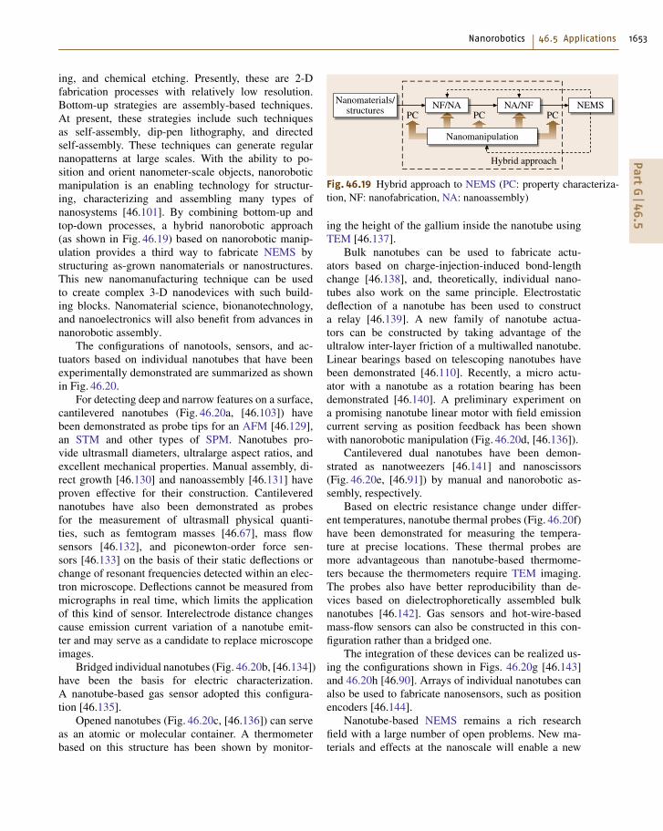
ing, and chemical etching. Presently, these are 2-Dfabrication processes with relatively low resolution.Bottom-up strategies are assembly-based techniques.At present, these strategies include such techniquesas self-assembly, dip-pen lithography, and directedself-assembly. These techniques can generate regularnanopatterns at large scales. With the ability to po-sition and orient nanometer-scale objects, nanoroboticmanipulation is an enabling technology for structur-ing, characterizing and assembling many types ofnanosystems [46.101]. By combining bottom-up andtop-down processes, a hybrid nanorobotic approach(as shown in Fig. 46.19) based on nanorobotic manip-ulation provides a third way to fabricate NEMS bystructuring as-grown nanomaterials or nanostructures.This new nanomanufacturing technique can be usedto create complex 3-D nanodevices with such build-ing blocks. Nanomaterial science, bionanotechnology,and nanoelectronics will also benefit from advances innanorobotic assembly.
The configurations of nanotools, sensors, and ac-tuators based on individual nanotubes that have beenexperimentally demonstrated are summarized as shownin Fig. 46.20.
For detecting deep and narrow features on a surface,cantilevered nanotubes (Fig. 46.20a, [46.103]) havebeen demonstrated as probe tips for an AFM [46.129],an STM and other types of SPM. Nanotubes pro-vide ultrasmall diameters, ultralarge aspect ratios, andexcellent mechanical properties. Manual assembly, di-rect growth [46.130] and nanoassembly [46.131] haveproven effective for their construction. Cantileverednanotubes have also been demonstrated as probesfor the measurement of ultrasmall physical quanti-ties, such as femtogram masses [46.67], mass flowsensors [46.132], and piconewton-order force sen-sors [46.133] on the basis of their static deflections orchange of resonant frequencies detected within an elec-tron microscope. Deflections cannot be measured frommicrographs in real time, which limits the applicationof this kind of sensor. Interelectrode distance changescause emission current variation of a nanotube emit-ter and may serve as a candidate to replace microscopeimages.
Bridged individual nanotubes (Fig. 46.20b, [46.134])have been the basis for electric characterization.A nanotube-based gas sensor adopted this configura-tion [46.135].
Opened nanotubes (Fig. 46.20c, [46.136]) can serveas an atomic or molecular container. A thermometerbased on this structure has been shown by monitor-
NEMSNA/NFNF/NAPC PCPC
Nanomaterials/structures
Nanomanipulation
Hybrid approach
Fig. 46.19 Hybrid approach to NEMS (PC: property characteriza-tion, NF: nanofabrication, NA: nanoassembly)
ing the height of the gallium inside the nanotube usingTEM [46.137].
Bulk nanotubes can be used to fabricate actu-ators based on charge-injection-induced bond-lengthchange [46.138], and, theoretically, individual nano-tubes also work on the same principle. Electrostaticdeflection of a nanotube has been used to constructa relay [46.139]. A new family of nanotube actua-tors can be constructed by taking advantage of theultralow inter-layer friction of a multiwalled nanotube.Linear bearings based on telescoping nanotubes havebeen demonstrated [46.110]. Recently, a micro actu-ator with a nanotube as a rotation bearing has beendemonstrated [46.140]. A preliminary experiment ona promising nanotube linear motor with field emissioncurrent serving as position feedback has been shownwith nanorobotic manipulation (Fig. 46.20d, [46.136]).
Cantilevered dual nanotubes have been demon-strated as nanotweezers [46.141] and nanoscissors(Fig. 46.20e, [46.91]) by manual and nanorobotic as-sembly, respectively.
Based on electric resistance change under differ-ent temperatures, nanotube thermal probes (Fig. 46.20f)have been demonstrated for measuring the tempera-ture at precise locations. These thermal probes aremore advantageous than nanotube-based thermome-ters because the thermometers require TEM imaging.The probes also have better reproducibility than de-vices based on dielectrophoretically assembled bulknanotubes [46.142]. Gas sensors and hot-wire-basedmass-flow sensors can also be constructed in this con-figuration rather than a bridged one.
The integration of these devices can be realized us-ing the configurations shown in Figs. 46.20g [46.143]and 46.20h [46.90]. Arrays of individual nanotubes canalso be used to fabricate nanosensors, such as positionencoders [46.144].
Nanotube-based NEMS remains a rich researchfield with a large number of open problems. New ma-terials and effects at the nanoscale will enable a new
PartG
46.5

1654 Part G Industrial Applications
a) Cantileverd b) Bridged c) Opened d) Telescoping
e) Parallel f) Crossed g) Vertical array h) Lateral array
Electrodes
Electrode(s)
CNTs
CNTs
Electrode(s)
Electrode(s)
Electrode
CNT
CNT
Electrode
Electrode
Electrode
Support/cathode Support/cathodeSupport/Cathode
CNTCNT
CNT
CNT
100 nm 1 µm 200 nm
1 µm1 µm 20 µm
100 nm
300 nm
1 µm
CNT MWNT
Fig. 46.20a–h Configurations of individual nanotube-based NEMS. Scale bars: (a) 1 μm (inset: 100 nm), (b) 200 nm,(c) 1 μm, (d) 100 nm, (e) and (f)1 μm, (g) 20 μm, and (h) 300 nm. All examples are from the authors’ work
family of sensors and actuators for the detection andactuation of ultrasmall quantities or objects with ul-trahigh precision and frequencies. Through randomspreading, direct growth, and nanorobotic manipula-tion, prototypes have been demonstrated. However, for
integration into NEMS, self-assembly processes willbecome increasingly important. Among them, we be-lieve that dielectrophoretic nanoassembly will playa significant role for large-scale production of 2-D reg-ular structures.
References
46.1 R.P. Feynman: There’s plenty of room at the bot-tom, Caltech Eng. Sci. 23, 22–36 (1960)
46.2 M.C. Roco, R.S. Williams, P. Alivisatos: Nanotech-nology research directions, Interag. Work. GroupNanosci. Eng. Technol. (IWGN) Workshop Rep.(Kluwer, Dordrecht 2000)
46.3 Committee on Technology,M.L. Downey,D.T. Moore,G.R. Bachula, D.M. Etter, E.F. Carey, L.A. Per-ine: National Nanotechnology Initiative: Lead-ing to the Next Industrial Revolution, A Re-port by the Interagency Working Group on
Nanoscience, Engineering and Technology (Na-tional Science and Technology Council, Washington2000)
46.4 K. Drexler: Nanosystems: Molecular Machinery,Manufacturing and Computation (Wiley Inter-science, New York 1992)
46.5 G. Binnig, H. Rohrer, C. Gerber, E. Weibel: Surfacestudies by scanning tunneling microscopy, Phys.Rev. Lett. 49, 57–61 (1982)
46.6 W.F. Degrado: Design of peptides and proteins,Adv. Protein Chem. 39, 51–124 (1998)
PartG
46

Nanorobotics References 1655
46.7 J.-M. Lehn: Supramolecular Chemistry: Conceptsand Perspectives (VCH, Weinheim 1995)
46.8 G.M. Whitesides, B. Grzybowski: Self-assembly atall scales, Science 295, 2418–2421 (2002)
46.9 M. Fujita, N. Fujita, K. Ogura, K. Yamaguchi: Spon-taneous assembling of ten small components intoa three-dimensionally interlocked compound con-sisting of the same two cage frameworks, Nature400, 52–55 (1999)
46.10 T. Ebefors, G. Stemme: Microrobotics. In: The MEMSHandbook, ed. by M. Gad-el-Hak (CRC, Boca Raton2002)
46.11 C.-J. Kim, A.P. Pisano, R.S. Muller: Silicon-processed overhanging microgripper, IEEE/ASMEJ. MEMS 1, 31–36 (1992)
46.12 C. Liu, T. Tsao, Y.-C. Tai, C.-M. Ho: Surface micro-machined magnetic actuators, Proc. 7th IEEE Int.Conf. Micro Electro Mech. Syst., Oiso (IEEE, Piscat-away 1994) pp. 57–62
46.13 J. Judy, D.L. Polla, W.P. Robbins: A linear piezoelec-tric stepper motor with submicron displacementand centimeter travel, IEEE Trans. Ultrason. Ferro-electr. Freq. Control 37, 428–437 (1990)
46.14 K. Nakamura, H. Ogura, S. Maeda, U. Sangawa,S. Aoki, T. Sato: Evaluation of the micro wobblermotor fabricated by concentric buildup process,Proc. 8th IEEE Int. Conf. Micro Electro Mech. Syst.,Amsterdam (IEEE, Piscataway 1995) pp. 374–379
46.15 A. Teshigahara, M. Watanabe, N. Kawahara,I. Ohtsuka, T. Hattori: Performance of a 7-mmmicrofabricated car, IEEE/ASME J. MEMS 4, 76–80(1995)
46.16 K.R. Udayakumar, S.F. Bart, A.M. Flynn, J. Chen,L.S. Tavrow, L.E. Cross, R.A. Brooks, D.J. Ehrlich:Ferroelectric thin-film ultrasonic micromotors,Proc. 4th IEEE Int. Conf. Micro Electro Mech. Syst.,Nara (IEEE, Piscataway 1991) pp. 109–113
46.17 W. Trimmer, R. Jebens: Actuators for micro robots,Proc. 1989 IEEE Int. Conf. Robot. Autom., Scottsdale(IEEE, Piscataway 1989) pp. 1547–1552
46.18 P. Dario, R. Valleggi, M.C. Carrozza, M.C. Montesi,M. Cocco: Review – Microactuators for microrobots:A critical survey, J. Micromech. Microeng. 2, 141–157(1992)
46.19 I. Shimoyama: Scaling in microrobots, Proc.IEEE/RSJ Intell. Robot. Syst., Pittsburgh (IEEE, Pis-cataway 1995) pp. 208–211
46.20 R.S. Fearing: Powering 3-dimensional microrobots:power density limitations. In: Tutorial on MicroMechatronics and Micro Robotics, Proc. IEEE Int.Conf. Robot. Autom, Leuven, ed. by G. Girait,P. Dario (IEEE, Piscataway 1998)
46.21 R.G. Gilbertson, J.D. Busch: A survey of micro-actuator technologies for future spacecraft mis-sions, J. Br. Interplanet. Soc. 49, 129–138 (1996)
46.22 M. Mehregany, P. Nagarkar, S.D. Senturia,J.H. Lang: Operation of microfabricated harmonicand ordinary side-drive motors, Proc. 3th IEEE Int.
Conf. Micro Electro Mech. Syst., Napa Valley (IEEE,Piscataway 1990) pp. 1–8
46.23 Y.C. Tai, L.S. Fan, R.S. Muller: IC-processed micro-motors: design, technology, and testing, Proc. 2ndIEEE Int. Conf. Micro Electro Mech. Syst., Salt LakeCity (IEEE, Piscataway 1989) pp. 1–6
46.24 T. Ohnstein, T. Fukiura, J. Ridley, U. Bonne: Mi-cromachined silicon microvalve, Proc. 3rd IEEE Int.Conf. Micro Electro Mech. Syst., Napa Valley (IEEE,Piscataway 1990) pp. 95–99
46.25 L.Y. Chen, S.L. Zhang, J.J. Yao, D.C. Thomas,N.C. MacDonald: Selective chemical vapor deposi-tion of tungsten for microdynamic structures, Proc.2nd IEEE Int. Conf. Micro Electro Mech. Syst., SaltLake City (IEEE, Piscataway 1989) pp. 82–87
46.26 K. Yanagisawa, H. Kuwano, A. Tago: An electro-magnetically driven microvalve, Proc. 7th Int. Conf.Solid-State Sens. Actuators, Yokohama (IEEE, Pis-cataway 1993) pp. 102–105
46.27 S. Brand: New applications of piezo-electric ac-tuators, Proc. 3rd Int. Conf. New Actuators (MesseBremen GmbH, Bremen 1992) p. 59
46.28 M. Esashi, S. Shoji, A. Nakano: Normally close mi-crovalve and micropump fabricated on a siliconwafer, Proc. 4th IEEE Int. Conf. Micro Electro Mech.Syst., Salt Lake City (IEEE, Piscataway 1989) pp. 29–34
46.29 R. Petrucci, K. Simmons: An introduction to piezo-electric crystals, Sens. Mag. May, 26–31 (1994)
46.30 G. Binnig, C.F. Quate, C. Gerber: Atomic force mi-croscope, Phys. Rev. Lett. 56, 93–96 (1986)
46.31 A. Ashkin, J.M. Dziedzic: Optical trapping and ma-nipulation of viruses and bacteria, Science 235,1517–1520 (1987)
46.32 F.H.C. Crick, A.F.W. Hughes: The physical propertiesof cytoplasm: A study by means of the magneticparticle method, Part I: Experimental, Exp. Cell Res.1, 37–80 (1950)
46.33 M.F. Yu, M.J. Dyer, G.D. Skidmore, H.W. Rohrs,X.K. Lu, K.D. Ausman, J.R. Von Ehr, R.S. Ruoff:Three-dimensional manipulation of carbon nano-tubes under a scanning electron microscope,Nanotechnology 10, 244–252 (1999)
46.34 L.X. Dong, F. Arai, T. Fukuda: 3-D nanoroboticmanipulation of nano-order objects inside SEM,Proc. 2000 Int. Symp. Micromechatron. Hum. Sci.,Nagoya (IEEE, Piscataway 2000) pp. 151–156
46.35 D.M. Eigler, E.K. Schweizer: Positioning singleatoms with a scanning tunneling microscope, Na-ture 344, 524–526 (1990)
46.36 P. Avouris: Manipulation of matter at the atomicand molecular levels, Acc. Chem. Res. 28, 95–102(1995)
46.37 M.F. Crommie, C.P. Lutz, D.M. Eigler: Confinementof electrons to quantum corrals on a metal surface,Science 262, 218–220 (1993)
46.38 L.J. Whitman, J.A. Stroscio, R.A. Dragoset, R.J. Cel-lota: Manipulation of adsorbed atoms and creation
PartG
46

1656 Part G Industrial Applications
of new structures on room-temperature surfaceswith a scanning tunneling microscope, Science 251,1206–1210 (1991)
46.39 I.-W. Lyo, P. Avouris: Field-induced nanometer-scale to atomic-scale manipulation of siliconsurfaces with the STM, Science 253, 173–176 (1991)
46.40 G. Dujardin, R.E. Walkup, P. Avouris: Dissociationof individual molecules with electrons from the tipof a scanning tunneling microscope, Science 255,1232–1235 (1992)
46.41 T.-C. Shen, C. Wang, G.C. Abeln, J.R. Tucker,J.W. Lyding, P. Avouris, R.E. Walkup: Atomic-scaledesorption through electronic and vibrational-excitation mechanisms, Science 268, 1590–1592(1995)
46.42 M.T. Cuberes, R.R. Schittler, J.K. Gimzewski:Room-temperature repositioning of individual C60
molecules at Cu steps: Operation of a molecularcounting device, Appl. Phys. Lett. 69, 3016–3018(1996)
46.43 H.J. Lee, W. Ho: Single-bond formation and char-acterization with a scanning tunneling microscope,Science 286, 1719–1722 (1999)
46.44 T. Yamamoto, O. Kurosawa, H. Kabata, N. Shi-mamoto, M. Washizu: Molecular surgery of DNAbased on electrostatic micromanipulation, IEEETrans. IA 36, 1010–1017 (2000)
46.45 C. Haber, D. Wirtz: Magnetic tweezers for DNA mi-cromanipulation, Rev. Sci. Instrum. 71, 4561–4570(2000)
46.46 D.M. Schäfer, R. Reifenberger, A. Patil, R.P. An-dres: Fabrication of two-dimensional arrays ofnanometer-size clusters with the atomic force mi-croscope, Appl. Phys. Lett. 66, 1012–1014 (1995)
46.47 T. Junno, K. Deppert, L. Montelius, L. Samuel-son: Controlled manipulation of nanoparticles withan atomic force microscope, Appl. Phys. Lett. 66,3627–3629 (1995)
46.48 P.E. Sheehan, C.M. Lieber: Nanomachining, ma-nipulation and fabrication by force microscopy,Nanotechnology 7, 236–240 (1996)
46.49 C. Baur, B.C. Gazen, B. Koel, T.R. Ramachandran,A.A.G. Requicha, L. Zini: Robotic nanomanip-ulation with a scanning probe microscope ina networked computing environment, J. Vac. Sci.Technol. B 15, 1577–1580 (1997)
46.50 R. Resch, C. Baur, A. Bugacov, B.E. Koel, A. Mad-hukar, A.A.G. Requicha, P. Will: Building andmanipulating 3-D and linked 2-D structures ofnanoparticles using scanning force microscopy,Langmuir 14, 6613–6616 (1998)
46.51 J. Hu, Z.-H. Zhang, Z.-Q. Ouyang, S.-F. Chen,M.-Q. Li, F.-J. Yang: Stretch and align virus innanometer scale on an atomically flat surface,J. Vac. Sci. Technol. B 16, 2841–2843 (1998)
46.52 M. Sitti, S. Horiguchi, H. Hashimoto: Controlledpushing of nanoparticles: Modeling and exper-
iments, IEEE/ASME Trans. Mechatron. 5, 199–211(2000)
46.53 M. Guthold, M.R. Falvo, W.G. Matthews, S. Paulson,S. Washburn, D.A. Erie, R. Superfine, F.P. Brooks Jr.,R.M. Taylor II: Controlled manipulation of molecu-lar samples with the nanoManipulator, IEEE/ASMETrans. Mechatron. 5, 189–198 (2000)
46.54 F. Arai, D. Andou, T. Fukuda: Micro manipulationbased on micro physics – strategy based on attrac-tive force reduction and stress measurement, Proc.IEEE/RSJ Int. Conf. Intell. Robot. Syst., Pittsburgh(IEEE, Piscataway 1995) pp. 236–241
46.55 L.X. Dong, F. Arai, T. Fukuda: 3-D nanorobotic ma-nipulations of nanometer scale objects, J. Robot.Mechatron. 13, 146–153 (2001)
46.56 H.W.P. Koops, J. Kretz, M. Rudolph, M. Weber,G. Dahm, K.L. Lee: Characterization and applicationof materials grown by electron-beam-induced de-position, Jpn. J. Appl. Phys. 33, 7099–7107 (1994)
46.57 S. Iijima: Helical microtubules of graphitic carbon,Nature 354, 56–58 (1991)
46.58 S.J. Tans, A.R.M. Verchueren, C. Dekker: Room-temperature transistor based on a single carbonnanotube, Nature 393, 49–52 (1998)
46.59 Y. Huang, X.F. Duan, Y. Cui, L.J. Lauhon, K.-H. Kim,C.M. Lieber: Logic gates and computation from as-sembled nanowire building blocks, Science 294,1313–1317 (2001)
46.60 A. Bachtold, P. Hadley, T. Nakanishi, C. Dekker:Logic circuits with carbon nanotube transistors,Science 294, 1317–1320 (2001)
46.61 R.H. Baughman, A.A. Zakhidov, W.A. de Heer: Car-bon nanotubes – the route toward applications,Science 297, 787–792 (2002)
46.62 N. Wang, Z.K. Tang, G.D. Li, J.S. Chen: Single-walled4 Å carbon nanotube arrays, Nature 408, 50–51(2000)
46.63 Z.W. Pan, S.S. Xie, B.H. Chang, C.Y. Wang, L. Lu,W. Liu, W.Y. Zhou, W.Z. Li, L.X. Qian: Very longcarbon nanotubes, Nature 394, 631–632 (1998)
46.64 H.W. Zhu, C.L. Xu, D.H. Wu, B.Q. Wei, R. Vajtai,P.M. Ajayan: Direct synthesis of long single-walledcarbon nanotube strands, Science 296, 884–886(2002)
46.65 M.J. Treacy, T.W. Ebbesen, J.M. Gibson: Exception-ally high Young’s modulus observed for individualcarbon nanotubes, Nature 381, 678–680 (1996)
46.66 E.W. Wong, P.E. Sheehan, C.M. Lieber: Nanobeammechanics: Elasticity, strength, and toughness ofnanorods and nanotubes, Science 277, 1971–1975(1997)
46.67 P. Poncharal, Z.L. Wang, D. Ugarte, W.A. deHeer: Electrostatic deflections and electromechan-ical resonances of carbon nanotubes, Science 283,1513–1516 (1999)
46.68 M.F. Yu, O. Lourie, M.J. Dyer, K. Moloni, T.F. Kelley,R.S. Ruoff: Strength and breaking mechanism of
PartG
46

Nanorobotics References 1657
multiwalled carbon nanotubes under tensile load,Science 287, 637–640 (2000)
46.69 A. Krishnan, E. Dujardin, T.W. Ebbesen, P.N. Yian-ilos, M.M.J. Treacy: Young’s modulus of single-walled nanotubes, Phys. Rev. B 58, 14–013–14–019(1998)
46.70 J.P. Salvetat, G.A.D. Briggs, J.-M. Bonard,R.R. Bacsa, A.J. Kulik, T. Stockli, N.A. Burnham,L. Forro: Elastic and shear moduli of single-walledcarbon nanotube ropes, Phys. Rev. Lett. 82, 944–947 (1999)
46.71 M.F. Yu, B.S. Files, S. Arepalli, R.S. Ruoff: Tensileloading of ropes of single wall carbon nanotubesand their mechanical properties, Phys. Rev. Lett.84, 5552–5555 (2000)
46.72 D.A. Walters, L.M. Ericson, M.J. Casavant, J. Liu,D.T. Colbert, K.A. Smith, R.E. Smalley: Elastic strainof freely suspended single-wall carbon nanotuberopes, Appl. Phys. Lett. 74, 3803–3805 (1999)
46.73 R. Saito, M. Fujita, G. Dresselhaus, M.S. Dres-selhaus: Electronic structure of graphene tubulesbased on C60, Phys. Rev. B 46, 1804–1811 (1992)
46.74 T.W. Ebbesen, H.J. Lezec, H. Hiura, J.W. Bennett,H.F. Ghaemi, T. Thio: Electrical conductivity of indi-vidual carbon nanotubes, Nature 382, 54–56 (1996)
46.75 H.J. Dai, E.W. Wong, C.M. Lieber: Probing elec-trical transport in nanomaterials: conductivity ofindividual carbon nanotubes, Science 272, 523–526(1996)
46.76 P. Kim, L. Shi, A. Majumdar, P.L. McEuen: Thermaltransport measurements of individual multiwallednanotubes, Phys. Rev. Lett. 87, 215502 (2001)
46.77 W.J. Liang, M. Bockrath, D. Bozovic, J.H. Hafner,M. Tinkham, H. Park: Fabry–Perot interference ina nanotube electron waveguide, Nature 411, 665–669 (2001)
46.78 S. Frank, P. Poncharal, Z.L. Wang, W.A. de Heer:Carbon nanotube quantum resistors, Science 280,1744–1746 (1998)
46.79 X.B. Zhang, D. Bernaerts, G. Van Tendeloo,S. Amelincks, J. Van Landuyt, V. Ivanov, J.B. Nagy,P. Lambin, A.A. Lucas: The texture of catalyticallygrown coil-shaped carbon nanotubules, Europhys.Lett. 27, 141–146 (1994)
46.80 X.Y. Kong, Z.L. Wang: Spontaneous polarization-induced nanohelixes, nanosprings, and nanoringsof piezoelectric nanobelts, Nano Lett. 3, 1625–1631(2003)
46.81 S.V. Golod, V.Y. Prinz, V.I. Mashanov, A.K. Gu-takovsky: Fabrication of conducting GeSi/Si micro-and nanotubes and helical microcoils, Semicond.Sci. Technol. 16, 181–185 (2001)
46.82 L. Zhang, E. Deckhardt, A. Weber, C. Schönen-berger, D. Grützmacher: Controllable fabrication ofSiGe/Si and SiGe/Si/Cr helical nanobelts, Nanotech-nology 16, 655–663 (2005)
46.83 D.J. Bell, L.X. Dong, Y. Sun, L. Zhang, B.J. Nel-son, D. Grützmacher: Manipulation of nanocoils
for nanoelectromagnets, Proc. 5th IEEE Conf.Nanotechnol., Nagoya (IEEE, Piscataway 2005)pp. 149–152
46.84 D.J. Bell, Y. Sun, L. Zhang, L.X. Dong, B.J. Nelson,D. Grützmacher: Three-dimensional nanospringsfor electromechanical sensors, Proc. 13th Int. Conf.Solid-State Sens. Actuators Microsyst., Seoul (IEEE,Piscataway 2005) pp. 15–18
46.85 S. Iijima, T. Ichihashi: Single-shell carbon nano-tubes of 1-nm diameter, Nature 363, 603–605(1993)
46.86 D.S. Bethune, C.H. Kiang, M.S. de Vries, G. Gorman,R. Savoy, J. Vazquez, R. Beyers: Cobalt-catalysedgrowth of carbon nanotubes with single-atomic-layer walls, Nature 363, 605–607 (1993)
46.87 R. Martel, T. Schmidt, H.R. Shea, T. Hertel,P. Avouris: Single- and multi-wall carbon nano-tube field-effect transistors, Appl. Phys. Lett. 73,2447–2449 (1998)
46.88 N.R. Franklin, Y.M. Li, R.J. Chen, A. Javey, H.J. Dai:Patterned growth of single-walled carbon nano-tubes on full 4-inch wafers, Appl. Phys. Lett. 79,4571–4573 (2001)
46.89 T. Rueckes, K. Kim, E. Joselevich, G.Y. Tseng, C.-L. Cheung, C.M. Lieber: Carbon nanotube-basednon-volatile random access memory for molecularcomputing, Science 289, 94–97 (2000)
46.90 A. Subramanian, B. Vikramaditya, L.X. Dong,D. Bell, B.J. Nelson: Micro and nanorobotic assem-bly using dielectrophoresis. In: Robotics: Scienceand Systems I, ed. by S. Thrun, G.S. Sukhatme,S. Schaal, O. Brock (MIT Press, Cambridge 2005)pp. 327–334
46.91 T. Fukuda, F. Arai, L.X. Dong: Assembly of nanode-vices with carbon nanotubes through nanoroboticmanipulations, Proc. IEEE 91, 1803–1818 (2003)
46.92 M.R. Falvo, G.J. Clary, R.M. Taylor, V. Chi,F.P. Brooks, S. Washburn, R. Superfine: Bendingand buckling of carbon nanotubes under largestrain, Nature 389, 582–584 (1997)
46.93 H.W.C. Postma, A. Sellmeijer, C. Dekker: Manip-ulation and imaging of individual single-walledcarbon nanotubes with an atomic force micro-scope, Adv. Mater. 12, 1299–1302 (2000)
46.94 H.W.C. Postma, M. de Jonge, Z. Yao, C. Dekker: Elec-trical transport through carbon nanotube junctionscreated by mechanical manipulation, Phys. Rev. B62, R10653–R10656 (2000)
46.95 T. Hertel, R. Martel, P. Avouris: Manipulation ofindividual carbon nanotubes and their interactionwith surfaces, J. Phys. Chem. B 102, 910–915 (1998)
46.96 P. Avouris, T. Hertel, R. Martel, T. Schmidt,H.R. Shea, R.E. Walkup: Carbon nanotubes:nanomechanics, manipulation, and electronic de-vices, Appl. Surf. Sci. 141, 201–209 (1999)
46.97 L. Roschier, J. Penttila, M. Martin, P. Hakonen,M. Paalanen, U. Tapper, E.I. Kauppinen, C. Jour-net, P. Bernier: Single-electron transistor made
PartG
46

1658 Part G Industrial Applications
of multiwalled carbon nanotube using scanningprobe manipulation, Appl. Phys. Lett. 75, 728–730(1999)
46.98 M. Ahlskog, R. Tarkiainen, L. Roschier, P. Hakonen:Single-electron transistor made of two crossingmultiwalled carbon nanotubes and its noise prop-erties, Appl. Phys. Lett. 77, 4037–4039 (2000)
46.99 M.R. Falvo, R.M. Taylor II, A. Helser, V. Chi,F.P. Brooks Jr, S. Washburn, R. Superfine:Nanometre-scale rolling and sliding of carbonnanotubes, Nature 397, 236–238 (1999)
46.100 M.R. Falvo, J. Steele, R.M. Taylor II, R. Superfine:Gearlike rolling motion mediated by commensu-rate contact: Carbon nanotubes on HOPG, Phys.Rev. B 62, R10665–R10667 (2000)
46.101 L.X. Dong: Nanorobotic manipulations of car-bon nanotubes. Ph.D. Thesis (Nagoya University,Nagoya 2003)
46.102 J.H. Hafner, C.-L. Cheung, T.H. Oosterkamp,C.M. Lieber: High-yield assembly of individualsingle-walled carbon nanotube tips for scanningprobe microscopies, J. Phys. Chem. B 105, 743–746(2001)
46.103 L.X. Dong, F. Arai, T. Fukuda: Electron-beam-induced deposition with carbon nanotube emit-ters, Appl. Phys. Lett. 81, 1919–1921 (2002)
46.104 L.X. Dong, F. Arai, T. Fukuda: 3-D nanoroboticmanipulations of multi-walled carbon nanotubes,Proc. 2001 IEEE Int. Conf. Robot. Autom. (ICRA2001),Seoul (IEEE, Piscataway 2001) pp. 632–637
46.105 L.X. Dong, F. Arai, T. Fukuda: Three-dimensionalnanorobotic manipulations of carbon nanotubes,J. Robot. Mechatron. JSME 14, 245–252 (2002)
46.106 L.X. Dong, F. Arai, T. Fukuda: Inter-process meas-urement of MWNT rigidity and fabrication ofMWNT junctions through nanorobotic manipu-lations, Conf. Proc. Nanonetw. Mater. Fuller.Nanotub. Relat. Mater., Vol. 590 (AIP, Melville 2001)pp. 71–74
46.107 L.X. Dong, F. Arai, T. Fukuda: Shape modification ofcarbon nanotubes and its applications in nanotubescissors, Proc. IEEE Int. Conf. Nanotechnol. (IEEE-NANO2002), Washington (IEEE, Piscataway 2002)pp. 443–446
46.108 L.X. Dong, F. Arai, T. Fukuda: Destructive construc-tions of nanostructures with carbon nanotubesthrough nanorobotic manipulations, IEEE/ASMETrans. Mechatron. 9, 350–357 (2004)
46.109 J. Cumings, P.G. Collins, A. Zettl: Peeling andsharpening multiwall nanotubes, Nature 406, 58(2000)
46.110 J. Cumings, A. Zettl: Low-friction nanoscale linearbearing realized from multiwall carbon nanotubes,Science 289, 602–604 (2000)
46.111 L.X. Dong, F. Arai, T. Fukuda: 3-D nanoassem-bly of carbon nanotubes through nanoroboticmanipulations, Proc. 2002 IEEE Int. Conf. Robot.
Autom. (ICRA2002), Washington (IEEE, Piscataway2002) pp. 1477–1482
46.112 L.X. Dong, F. Arai, T. Fukuda: Mechanochemicalnanorobotic manipulations of carbon nanotubes,Jpn. J. Appl. Phys. 42, 295–298 (2003)
46.113 R. Saito, G. Dresselhaus, M.S. Dresselhaus: Tunnel-ing conductance of connected carbon nanotubes,Phys. Rev. B 53, 2044–2050 (1996)
46.114 L. Chico, V.H. Crespi, L.X. Benedict, S.G. Louie,M.L. Cohen: Pure carbon nanoscale devices: nano-tube heterojunctions, Phys. Rev. Lett. 76, 971–974(1996)
46.115 M. Menon, D. Srivastava: Carbon nanotube‘T junctions’: nanoscale metal–semiconductor–metal contact devices, Phys. Rev. Lett. 79,4453–4456 (1997)
46.116 Z. Yao, H.W.C. Postma, L. Balents, C. Dekker: Carbonnanotube intramolecular junctions, Nature 402,273–276 (1999)
46.117 H.W.C. Postma, T. Teepen, Z. Yao, M. Grifoni,C. Dekker: Carbon nanotube single-electron tran-sistors at room temperature, Science 293, 76–79(2001)
46.118 M.S. Fuhrer, L. Shih, M. Forero, Y.-G. Yoon,M.S.C. Mazzoni, H.J. Choi, J. Ihm, S.G. Louie,A. Zettl, P.L. McEuen: Crossed nanotube junctions,Science 288, 494–497 (2000)
46.119 T. Rueckes, K. Kim, E. Joselevich, G.Y. Treng,C.L. Cheung, C.M. Lieber: Carbon nanotube-basednonvolatile random access memory for molecularcomputing science, Science 289, 94–97 (2000)
46.120 A.G. Rinzler, J.H. Hafner, P. Nikolaev, L. Lou,S.G. Kim, D. Tománek, P. Nordlander, D.T. Colbert,R.E. Smalley: Unraveling nanotubes: field emissionfrom an atomic wire, Science 269, 1550–1553 (1995)
46.121 Y. Saito, K. Hamaguchi, K. Hata, K. Uchida,Y. Tasaka, F. Ikazaki, M. Yumura, A. Kasaya,Y. Nishina: Conical beams from open nanotubes,Nature 389, 554 (1997)
46.122 S.C. Minne, G. Yaralioglu, S.R. Manalis, J.D. Adams,J. Zesch, A. Atalar, C.F. Quate: Automated parallelhigh-speed atomic force microscopy, Appl. Phys.Lett. 72, 2340–2342 (1998)
46.123 G.D. Skidmore, E. Parker, M. Ellis, N. Sarkar,R. Merkle: Exponential assembly, Nanotechnology11, 316–321 (2001)
46.124 Y. Cui, Q.Q. Wei, H.K. Park, C.M. Lieber: Nanowirenanosensors for highly sensitive and selective de-tection of biological and chemical species, Science293, 1289–1292 (2001)
46.125 Y. Sun, B.J. Nelson: Microrobotic cell injection,Proc. 2001 IEEE Int. Conf. Robot. Autom. (ICRA2001),Seoul (IEEE, Piscataway 2001) pp. 620–625
46.126 Y. Sun, B.J. Nelson: Autonomous injection of bio-logical cells using visual servoing, Int. Symp. Exp.Robot. (ISER) (Lecture Notes Control Inform. Sci.,Hawaii 2000) pp. 175–184
PartG
46

Nanorobotics References 1659
46.127 Y. Sun, B.J. Nelson, D.P. Potasek, E. Enikov: A bulkmicrofabricated multi-axis capacitive cellular forcesensor using transverse comb drives, J. Micromech.Microeng. 12, 832–840 (2002)
46.128 Y. Sun, K. Wan, K.P. Roberts, J.C. Bischof,B.J. Nelson: Mechanical property characterizationof mouse zona pellucida, IEEE Trans. Nanobiosci. 2,279–286 (2003)
46.129 H.J. Dai, J.H. Hafner, A.G. Rinzler, D.T. Colbert,R.E. Smalley: Nanotubes as nanoprobes in scan-ning probe microscopy, Nature 384, 147–150 (1996)
46.130 J.H. Hafner, C.L. Cheung, C.M. Lieber: Growth ofnanotubes for probe microscopy tips, Nature 398,761–762 (1999)
46.131 H. Nishijima, S. Kamo, S. Akita, Y. Nakayama,K.I. Hohmura, S.H. Yoshimura, K. Takeyasu:Carbon-nanotube tips for scanning probe mi-croscopy: preparation by a controlled process andobservation of deoxyribonucleic acid, Appl. Phys.Lett. 74, 4061–4063 (1999)
46.132 L.X. Dong, F. Arai, M. Nakajima, P. Liu, T. Fukuda:Nanotube devices fabricated in a nano laboratory,Proc. 2003 IEEE Int. Conf. Robot. Autom. (ICRA2003),Taipei (IEEE, Piscataway 2003) pp. 3624–3629
46.133 M. Nakajima, F. Arai, L.X. Dong, T. Fukuda:Pico-Newton order force measurement using a cal-ibrated carbon nanotube probe inside a scanningelectron microscope, J. Robot. Mechatron. JSME16(2), 155–162 (2004)
46.134 A. Subramanian, B.J. Nelson, L.X. Dong, D. Bell: Di-electrophoretic nanoassembly of nanotube-basedNEMS with nanoelectrodes, 6th IEEE Int. Symp. As-sem. Task Plan., Montréal (IEEE, Piscataway 2005)pp. 200–205
46.135 J. Kong, N.R. Franklin, C.W. Zhou, M.G. Chapline,S. Peng, K.J. Cho, H.J. Dai: Nanotube molecular
wires as chemical sensors, Science 287, 622–625(2000)
46.136 L.X. Dong, B.J. Nelson, T. Fukuda, F. Arai: Towardslinear nano servomotors with integrated positionsensing, Proc. 2005 IEEE Int. Conf. Robot. Autom.,Barcelona (IEEE, Piscataway 2005) pp. 867–872
46.137 Y.H. Gao, Y. Bando: Carbon nanothermometer con-taining gallium, Nature 415, 599 (2002)
46.138 R.H. Baughman, C.X. Cui, A.A. Zakhidov, Z. Iqbal,J.N. Barisci, G.M. Spinks, G.G. Wallace, A. Mazzoldi,D. De Rossi, A.G. Rinzler, O. Jaschinski, S. Roth,M. Kertesz: Carbon nanotube actuators, Science284, 1340–1344 (1999)
46.139 S.W. Lee, D.S. Lee, R.E. Morjan, S.H. Jhang,M. Sveningsson, O.A. Nerushev, Y.W. Park,E.E.B. Campbell: A three-terminal carbon nano-relay, Nano Lett. 4, 2027–2030 (2004)
46.140 A.M. Fennimore, T.D. Yuzvinsky, W.-Q. Han,M.S. Fuhrer, J. Cumings, A. Zettl: Rotational ac-tuators based on carbon nanotubes, Nature 424,408–410 (2003)
46.141 P. Kim, C.M. Lieber: Nanotube nanotweezers, Sci-ence 286, 2148–2150 (1999)
46.142 C.K.M. Fung, V.T.S. Wong, R.H.M. Chan, W.J. Li:Dielectrophoretic batch fabrication of bundledcarbon nanotube thermal sensors, IEEE Trans. Nan-otech. 3, 395–403 (2004)
46.143 A. Subramanian, L.X. Dong, B.J. Nelson: Selectiveeradication of individual nanotubes from verti-cally aligned arrays, Proc. 2005 IEEE/ASME Int. Conf.Adv. Intell. Mechatron., Monterey (IEEE, Piscataway2005) pp. 105–110
46.144 L.X. Dong, A. Subramanian, B.J. Nelson: Nano en-coders based on arrays of single nanotube emitter,Proc. 5th IEEE Conf. Nanotechnol., Nagoya (IEEE,Piscataway 2005) pp. 211–214
PartG
46