1.8-v-5.5-vinput, 3.3-voutput, high efficiency dc/dc · pdf fileslva334b– october...
TRANSCRIPT
Application ReportSLVA334B–October 2009–Revised June 2010
1.8-V - 5.5-V Input, 3.3-V Output, High Efficiency DC/DCConverter
................................................................................................... PMP - DC/DC Low-Power Converters
ABSTRACT
This reference design is presented to help application designers and others who are trying to use theMSP430 in a system with an input voltage in the range of 1.8 V to 5.5 V, and who must increase theapplication run time by making use of the complete battery voltage range while still maintaining highefficiency over the entire battery life.
Contents1 Introduction .................................................................................................................. 22 Requirements ................................................................................................................ 33 Description of Power Solution ............................................................................................. 54 Power Supply Option 1: TPS63031 ...................................................................................... 55 Power Supply Option 2: TPS63001 ...................................................................................... 86 Inductor Selection ......................................................................................................... 137 Capacitor Selection ........................................................................................................ 138 General Layout Considerations .......................................................................................... 149 References ................................................................................................................. 15
List of Figures
1 TPS63030EVM-417 Schematic ........................................................................................... 6
2 Turn ON into Load, VIN = 2.2 V............................................................................................ 7
3 Output Ripple, VIN = 2.2 V ................................................................................................. 7
4 PMP4778 Reference Design Schematic................................................................................. 8
5 Startup........................................................................................................................ 9
6 Startup ....................................................................................................................... 9
7 Startup........................................................................................................................ 9
8 Startup ....................................................................................................................... 9
9 Startup........................................................................................................................ 9
10 Startup........................................................................................................................ 9
11 Output Ripple Voltage .................................................................................................... 10
12 Output Ripple Voltage .................................................................................................... 10
13 Output Ripple Voltage .................................................................................................... 10
14 Load Transient ............................................................................................................. 10
15 Load Transient ............................................................................................................. 11
16 Load Transient ............................................................................................................. 11
17 Switching Node Waveform ............................................................................................... 11
18 Switching Node Waveform ............................................................................................... 11
19 Switching Node Waveform ............................................................................................... 12
20 Efficiency vs Output Current ............................................................................................. 12
List of Tables
All trademarks are the property of their respective owners.
1SLVA334B–October 2009–Revised June 2010 1.8-V - 5.5-V Input, 3.3-V Output, High Efficiency DC/DC Converter
Copyright © 2009–2010, Texas Instruments Incorporated
Introduction www.ti.com
1 CC43 Family Power Requirements....................................................................................... 3
2 MSP430x1xx Family Power Requirements ............................................................................. 3
3 MSP430x2xx Family Power Requirements ............................................................................. 3
4 MSP430x4xx Family Power Requirements ............................................................................. 4
5 MSP430x5xx Family Power Requirements ............................................................................. 5
6 List of Materials TPS63030EVM-417 .................................................................................... 7
7 List of Materials PMP4778................................................................................................. 8
8 TPS6303x List of Inductors .............................................................................................. 13
9 TPS6300x List of Inductors .............................................................................................. 13
10 Related Documents ....................................................................................................... 15
1 Introduction
This reference design is for the MSP430 family of microcontroller devices and Stellaris devices, andaccounts for the voltage and current requirements as described herein. The MSP430 devices require onlya single voltage supply; no sequencing is required. The operating input voltage for this reference design isbetween 1.8 V to 5.5 V, allowing applications operating from a battery supply to benefit from the completebattery capacity. This design is optimized for a wide input voltage range, a small solution size, and lowcomponent count.
For more information and other reference designs, see the Reference section at the end of this documentor visit www.ti.com/processorpower.
1.1 Features• 1.8-V to 5.5-V input voltage range• Fixed 3.3-V output eliminates need for external voltage-setting resistors• Capable of driving up to 800 mA when operating in boost mode (TPS63001)• Capable of driving up to 500 mA when operating in boost mode (TPS63031)• High efficiency (up to 94%)• Low quiescent current (less than 50 µA)• Small QFN packages: 2.5 mm × 2.5 mm (TPS63031) or 3 mm x 3 mm (TPS63001)
2 1.8-V - 5.5-V Input, 3.3-V Output, High Efficiency DC/DC Converter SLVA334B–October 2009–Revised June 2010
Copyright © 2009–2010, Texas Instruments Incorporated
www.ti.com Requirements
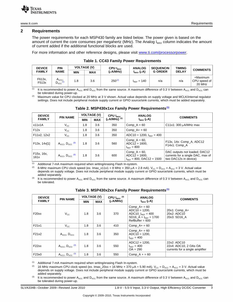
2 Requirements
The power requirements for each MSP430 family are listed below. The power given is based on theamount of current the core consumes per megahertz (MHz). The Analog IMAX column indicates the amountof current added if the additional functional blocks are used.
For more information and other reference designs, please visit www.ti.com/processorpower.
Table 1. CC43 Family Power Requirements
VOLTAGE (V)DEVICE PIN CPU IMAX ANALOG SEQUENCIN TIMING COMMENTSFAMILY NAME (mA/MHz) IMAX (mA) G ORDER DELAYMIN MAX
+MaximumF613x, AVCC, 1.8 3.6 250 (2) IREF = 140 n/a n/a CPU speed ofF513x DVCC(1)
20 MHz(1) It is recommended to power AVCC and DVCC from the same source. A maximum difference of 0.3 V between AVCC and DVCC can
be tolerated during power-up.(2) Maximum value for CPU clocked at 20 MHz at 3 V shown. Actual value depends on supply voltage and MCLK/internal regulator
settings. Does not include peripheral module supply current or GPIO source/sink currents, which must be added separately.
Table 2. MSP430x1xx Family Power Requirements (1)
VOLTAGE (V)DEVICE CPU IMAX ANALOGPIN NAME COMMENTSFAMILY (mA/MHz) (2) IMAX (mA)MIN MAX
x11x1A VCC 1.8 3.6 350 Comp_A = 60 C11x1: 300 mA/MHz max
F12x VCC 1.8 3.6 350 Comp_A+ = 60
F11x2, 12x2 VCC 1.8 3.6 350 ADC10 = 1200, IREF = 400
Comp_A = 60, F13x, 14x: Comp_A, ADC12F13x, 14x[1] AVCC, DVCC(3) 1.8 3.6 560 ADC12 = 1600, F14x1: Comp_AIREF = 800
Comp_A = 60, DAC outputs not loaded; DAC12F15x, 16x, AVCC, DVCC(3) 1.8 3.6 600 ADC12 = 1600, currents for a single DAC, max of161x IREF = 800, DAC12 = 1500 two DAC12s in device)
(1) Additional 7-mA maximum required when writing/erasing Flash In-system.(2) 8-MHz maximum CPU clock speed (ex. Imax_x11x1 = 8 MHz × 350 mA = 2.8 mA). VCC = DVCC = AVCC = 3 V. Actual value
depends on supply voltage. Does not include peripheral module supply current or GPIO source/sink currents, which must beadded separately.
(3) It is recommended to power AVCC and DVCC from the same source. A maximum difference of 0.3 V between AVCC and DVCC canbe tolerated.
Table 3. MSP430x2xx Family Power Requirements (1)
VOLTAGE (V)DEVICE CPU IMAX(2) ANALOGPIN NAME COMMENTSFAMILY (mA/MHz) IMAX (mA)MIN MAX
Comp_A+ = 60ADC10 = 1200, 20x1: Comp_A+
F20xx VCC 1.8 3.6 370 ADC10_IREF = 400 20x2: ADC10SD16_A + IREF = 1700 20x3: SD16_ARefBuffer = 600
F21x1 VCC 1.8 3.6 410 Comp_A+ = 60
Comp_A+ = 60F21x2 AVCC, DVCC 1.8 3.6 350 ADC10 = 1200,
IREF = 400
ADC12 = 1200, 22x2: ADC10F22xx AVCC, DVCC
(3) 1.8 3.6 550 IREF = 400 22x4: ADC10, 2 OAs OAOA = 290 currents for a single amplifier
F23x0 AVCC, DVCC(3) 1.8 3.6 550 Comp_A + = 60
(1) Additional 7-mA maximum required when writing/erasing Flash In-system.(2) 16 MHz maximum CPU clock speed (ex. Imax_20xx = 16 MHz × 370 mA = 5.90 mA). VCC = DVCC = AVCC = 3 V. Actual value
depends on supply voltage. Does not include peripheral module supply current or GPIO source/sink currents, which must beadded separately.
(3) It is recommended to power AVCC and DVCC from the same source. A maximum difference of 0.3 V between AVCC and DVCC canbe tolerated during power-up.
3SLVA334B–October 2009–Revised June 2010 1.8-V - 5.5-V Input, 3.3-V Output, High Efficiency DC/DC Converter
Copyright © 2009–2010, Texas Instruments Incorporated
Requirements www.ti.com
Table 3. MSP430x2xx Family Power Requirements (1) (continued)
VOLTAGE (V)DEVICE CPU IMAX(2) ANALOGPIN NAME COMMENTSFAMILY (mA/MHz) IMAX (mA)MIN MAX
Comp_A + = 60, 224x1: Comp_A+F23x, 24x[1], AVCC, DVCC(3) 1.8 3.6 445 ADC12 = 1000, 23x, 24x, 2410: Comp_A+,2410 IREF = 700 ADC12
241x: Comp_A+, ADC12Comp_A + = 60, 261x: Comp_A+, ADC12, twoADC12 = 1000,F241x, 261x AVCC, DVCC(3) 1.8 3.6 560 DAC12s DAC12 outputs notIREF = 700 loaded; DAC12 currents for aDAC12 = 1500 single DAC
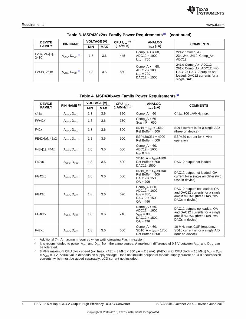
Table 4. MSP430x4xx Family Power Requirements (1)
VOLTAGE (V)DEVICE CPU IMAX ANALOGPIN NAME (2) COMMENTSFAMILY (mA/MHz) (3) IMAX (mA)MIN MAX
x41x AVCC, DVCC 1.8 3.6 350 Comp_A = 60 C41x: 300 mA/MHz max
Comp_A = 60FW42x AVCC, DVCC 1.8 3.6 350 Scan IF = 650
SD16 + IREF = 1550 SD16 current is for a single A/DF42x AVCC, DVCC 1.8 3.6 500 Ref Buffer = 600 (three on device)
ESP430CE1 = 4900 ESP430 current for 4-MHzFE42x[a], 42x2 AVCC, DVCC 1.8 3.6 500 Ref Buffer = 600 operation
Comp_A = 60,F43x[1], F44x AVCC, DVCC 1.8 3.6 560 ADC12 = 1600,
IREF = 800
SD16_A + IREF=1800F42x0 AVCC, DVCC 1.8 3.6 520 Ref Buffer = 600 DAC12 output not loaded
DAC12=1500
SD16_A + IREF=1800 DAC12 output not loaded; OARef Buffer = 600FG42x0 AVCC, DVCC 1.8 3.6 560 current for a single amplifier (twoDAC12 = 1500, OAs in device)OA = 290
Comp_A = 60, DAC12 outputs not loaded; OAADC12 = 1600, and DAC12 currents for a singleFG43x AVCC, DVCC 1.8 3.6 570 IREF = 800, amplifier/DAC (three OAs, twoDAC12 = 1500, DACs in device)OA = 490
Comp_A = 60, DAC12 outputs no loaded; OAADC12 = 1600, and DAC12 currents for a singleFG46xx AVCC, DVCC 1.8 3.6 740 VREF = 800, amplifier/DAC (three OAs, twoDAC12 = 1500, DACs in device)OA = 490
Comp_A = 60, 16 MHz max CUP frequency;F47xx AVCC, DVCC 1.8 3.6 560 SD16_A + IREF = 1700 SD16 current is for a single A/D
Ref Buffer = 600 (four on device)(1) Additional 7-mA maximum required when writing/erasing Flash In-system.(2) It is recommended to power AVCC and DVCC from the same source. A maximum difference of 0.3 V between AVCC and DVCC can
be tolerated.(3) 8 MHz maximum CPU clock speed (ex. Imax_x41x = 8 MHz × 350 mA = 2.8 mA). (F47xx max CPU clock = 16 MHz) VCC = DVCC
= AVCC = 3 V. Actual value depends on supply voltage. Does not include peripheral module supply current or GPIO source/sinkcurrents, which must be added separately. LCD current not included.
4 1.8-V - 5.5-V Input, 3.3-V Output, High Efficiency DC/DC Converter SLVA334B–October 2009–Revised June 2010
Copyright © 2009–2010, Texas Instruments Incorporated

www.ti.com Description of Power Solution
Table 5. MSP430x5xx Family Power Requirements (1)
VOLTAGE (V)DEVICE CPU IMAX ANALOGPIN NAME COMMENTSFAMILY (mA/MHz) (2) IMAX (mA)MIN MAX
ADC12_A = 220, 18 MHz maximum CPU clockF54xx AVCC, DVCC(3) 2.2 3.6 348 IREF = 190 speed
(1) Additional 5-mA maximum required when writing/erasing Flash In-system.(2) 16 MHz maximum at 3-V CPU clock speed. Actual value depends on supply voltage and MCLK/internal regulator settings. Does
not include peripheral module supply current or GPIO source/sink currents, which must be added separately.(3) It is recommended to power AVCC and DVCC from the same source. A maximum difference of 0.3 V between AVCC and DVCC can
be tolerated during power-up.
3 Description of Power Solution
Using a buck-boost topology for battery-driven applications enables users to benefit fully from theavailable charge given from the chemistry.
The TPS630xx devices belong to a fully-integrated family of converters that automatically regulate thepreset output voltage over the entire input voltage range of 1.8 V to 5.5 V.
In the case of a fixed 3.3-V output, the converter operates in step-down mode for periods when the inputvoltage is greater than 3.3 V. Once the input voltage drops below the required 3.3 V, the converterautomatically transitions into boost mode without the need of any external control signals or circuitry.
The buck-boost converter architecture is based on a fixed-frequency pulse-width-modulation (PWM)controller using synchronous rectification to obtain maximum efficiency. At low load currents, the converterenters a Power Save mode to maintain high efficiency over a wide load current range. Power Save modecan be disabled using the PS/SYNC pin, forcing the converter to operate at a fixed switching frequency.
During shutdown, the load is disconnected from the battery.
In cases where budgeting the power of the TPS63001 is required but the overall solution size is critical,the TPS63011 in an available WCSP is recommended.
In applications where overall power consumption is a critical parameter, the MSP430 should operate at alower input voltage such as 2.2 V; this lower input level allow all blocks to run optimally. In this case, seethe adjustable versions of the TPS63000 and TPS63030 buck-boost converter device families.
4 Power Supply Option 1: TPS63031
The TPS63031 supports 500 mA when operating in boost mode (VIN > 2.4V) and greater than 800 mAwhen working in step-down mode (VIN = 3.6 V to 5.5 V). The overall solution size and the entire deviceefficiency, as well as the provided power budget, make this converter an ideal fit for portable,battery-driven applications. For a more detailed description of the device characteristics as well asfunctionality, refer to the device data sheet.
The device can be evaluated by itself using the TPS63030EVM-417 evaluation module. By default, theEVM contains the adjustable device TPS63030. In order to evaluate the 3.3-V version, simply replacedevice U1 on the EVM board with the TPS63031 device. Furthermore, R1 must be replaced with a 0-Ωresistor; the R2 position remains open.
The following description as well as the results are taken from the TPS63030EVM-417 User Guide.
5SLVA334B–October 2009–Revised June 2010 1.8-V - 5.5-V Input, 3.3-V Output, High Efficiency DC/DC Converter
Copyright © 2009–2010, Texas Instruments Incorporated
Power Supply Option 1: TPS63031 www.ti.com
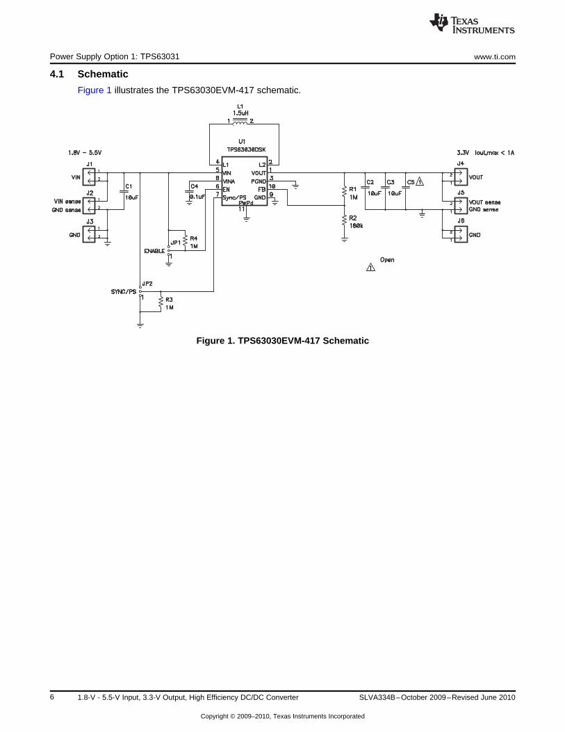
4.1 Schematic
Figure 1 illustrates the TPS63030EVM-417 schematic.
Figure 1. TPS63030EVM-417 Schematic
6 1.8-V - 5.5-V Input, 3.3-V Output, High Efficiency DC/DC Converter SLVA334B–October 2009–Revised June 2010
Copyright © 2009–2010, Texas Instruments Incorporated
Enable 5 V/div
Output Voltage 2 V/div
Voltage at L2 2 V/div
Inductor Current500 mA/div
Vin 2.4 V, Rload = 12 W
t - Time - 400 s/divm
Output Ripple 10 mV/div
Voltage at L2 2 V/div
TPS63030 - Output RippleVIN = 2.2 V,VOUT = 3.3 V,150 mA Load
Voltage at L2 2 V/div
t - Time - 200 ns/div
www.ti.com Power Supply Option 1: TPS63031
4.2 List of Materials TPS63030EVM-417
Table 6 shows the bill of materials (BOM) for this design.
Table 6. List of Materials TPS63030EVM-417
QTY REF DES VALUE DESCRIPTION SIZE PART NUMBER MFR
3 C1, C2, C3 10 mF Capacitor, ceramic, 6.3-V, X7R, 10% 0603 GRM188R60J106ME84D Murata
1 C4 0.1 mF Capacitor, ceramic, 6.3-V, X7R, 10% 0603 GRM188R70J104KA01B Murata
0 C5 Open Capacitor, ceramic, 6.3-V, X7R, 10% 0603 GRM188R60J106ME84D Murata
1 L1 1.5 mH Inductor, SMT, 1.3-A, 110-mΩ 0.118 × 0.118 LPS3015-152MLB Coilcraft
3 R1, R3, R4 1 MΩ Resistor, chip, 1/16-W, 1% 0603 Std Std
1 R2 180 kΩ Resistor, chip, 1/16-W, 1% 0603 Std Std
1 U1 IC, dc/dc converter DSK TPS63030DSK TI
4.3 Test Results TPS63031
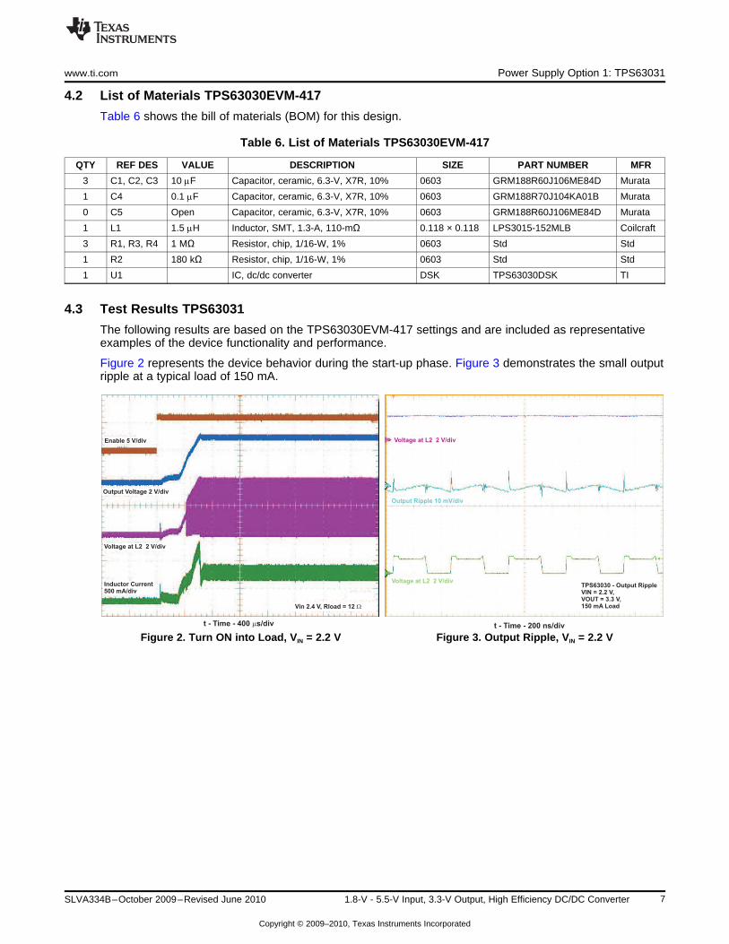
The following results are based on the TPS63030EVM-417 settings and are included as representativeexamples of the device functionality and performance.
Figure 2 represents the device behavior during the start-up phase. Figure 3 demonstrates the small outputripple at a typical load of 150 mA.
Figure 2. Turn ON into Load, VIN = 2.2 V Figure 3. Output Ripple, VIN = 2.2 V
7SLVA334B–October 2009–Revised June 2010 1.8-V - 5.5-V Input, 3.3-V Output, High Efficiency DC/DC Converter
Copyright © 2009–2010, Texas Instruments Incorporated
4
5
8
L1
VIN
VINA
U1
TPS63001DRC
C3
10 mF
UDG-09083
7
6
SYNC/PS
EN
2
1
L2
VOUT
10
9
FB
GND
C2
10 mF
R1
0 W
L1
2.2 mH
J31
2
J41
2GND
3.3 VOUT
1.2 A (max)
3PGND
C1
10 mF
J11
2
J21
2GND
VIN
1.8 V
to
5.5 V
Power Supply Option 2: TPS63001 www.ti.com
5 Power Supply Option 2: TPS63001
The TPS63001 supports 800 mA when operating in boost mode (VIN > 2.4 V) and greater than 1200 mAwhen working in step-down mode (VIN = 3.6 V to 5.5 V). The overall solution size and the entire deviceefficiency, as well as the provided power budget, make the converter an ideal fit for portable,battery-driven applications. For a more detailed description of the device characteristics as well asfunctionality, refer to the device data sheet.
The device can be evaluated by itself using the TPS63000EVM-148 evaluation module. By default, theEVM contains the TPS63000 adjustable device. In order to evaluate the 3.3-V version, simply replacedevice U1 on the EVM board with the TPS63001. Furthermore, R1 must be replaced with a 0-Ω resistor;the R2 position remains open.
The following description as well as the results are taken from the TPS63000EVM-148 Users Guide.
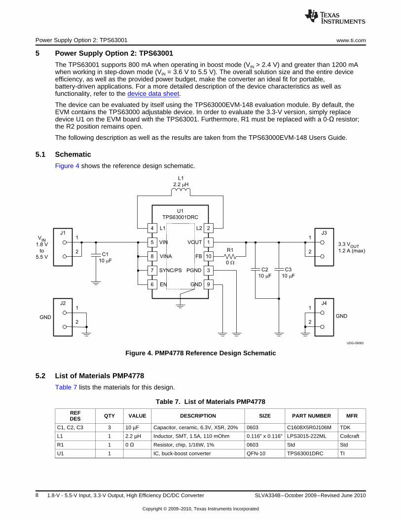
5.1 Schematic
Figure 4 shows the reference design schematic.
Figure 4. PMP4778 Reference Design Schematic
5.2 List of Materials PMP4778
Table 7 lists the materials for this design.
Table 7. List of Materials PMP4778
REF QTY VALUE DESCRIPTION SIZE PART NUMBER MFRDES
C1, C2, C3 3 10 µF Capacitor, ceramic, 6.3V, X5R, 20% 0603 C1608X5R0J106M TDK
L1 1 2.2 µH Inductor, SMT, 1.5A, 110 mOhm 0.116" x 0.116" LPS3015-222ML Coilcraft
R1 1 0 Ω Resistor, chip, 1/16W, 1% 0603 Std Std
U1 1 IC, buck-boost converter QFN-10 TPS63001DRC TI
8 1.8-V - 5.5-V Input, 3.3-V Output, High Efficiency DC/DC Converter SLVA334B–October 2009–Revised June 2010
Copyright © 2009–2010, Texas Instruments Incorporated
www.ti.com Power Supply Option 2: TPS63001
5.3 Test Results TPS63001
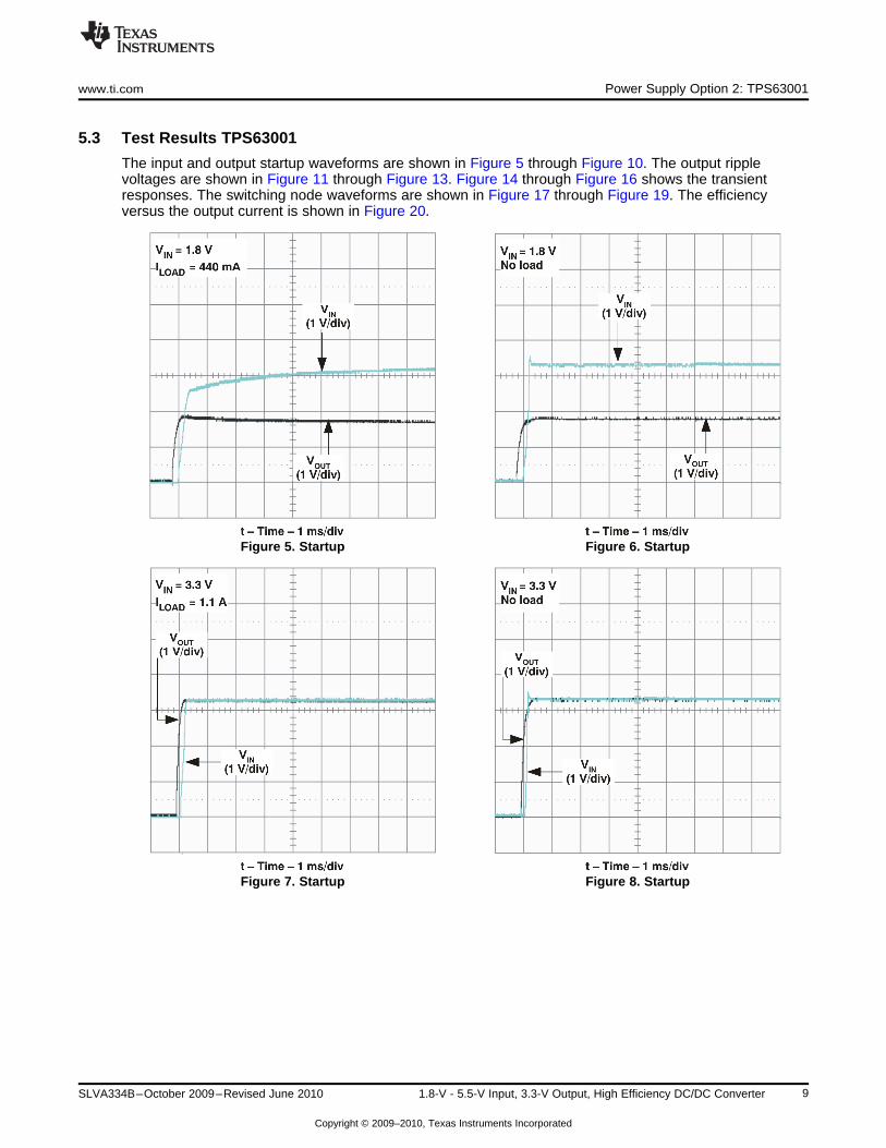
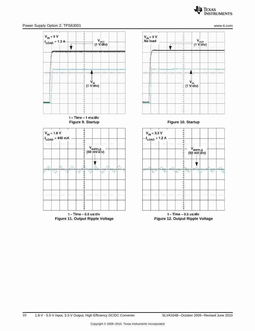
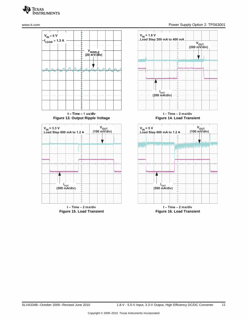
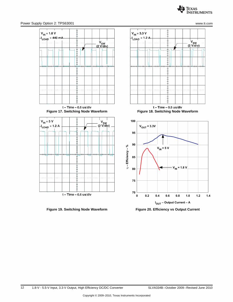
The input and output startup waveforms are shown in Figure 5 through Figure 10. The output ripplevoltages are shown in Figure 11 through Figure 13. Figure 14 through Figure 16 shows the transientresponses. The switching node waveforms are shown in Figure 17 through Figure 19. The efficiencyversus the output current is shown in Figure 20.
Figure 5. Startup Figure 6. Startup
Figure 7. Startup Figure 8. Startup
9SLVA334B–October 2009–Revised June 2010 1.8-V - 5.5-V Input, 3.3-V Output, High Efficiency DC/DC Converter
Copyright © 2009–2010, Texas Instruments Incorporated
Power Supply Option 2: TPS63001 www.ti.com
Figure 9. Startup Figure 10. Startup
Figure 11. Output Ripple Voltage Figure 12. Output Ripple Voltage
10 1.8-V - 5.5-V Input, 3.3-V Output, High Efficiency DC/DC Converter SLVA334B–October 2009–Revised June 2010
Copyright © 2009–2010, Texas Instruments Incorporated
VIN
= 1.8 V
Load Step 200 mA to 400 mA
IOUT
(200 mA/div)
VOUT
(200 mV/div)
t – Time – 2 ms/div
VIN
= 3.3 V
Load Step 600 mA to 1.2 A
IOUT
(500 mA/div)
VOUT
(100 mV/div)
t – Time – 2 ms/div t – Time – 2 ms/div
IOUT
(500 mA/div)
VIN
= 5 V
Load Step 600 mA to 1.2 A
VOUT
(100 mV/div)
www.ti.com Power Supply Option 2: TPS63001
Figure 13. Output Ripple Voltage Figure 14. Load Transient
Figure 15. Load Transient Figure 16. Load Transient
11SLVA334B–October 2009–Revised June 2010 1.8-V - 5.5-V Input, 3.3-V Output, High Efficiency DC/DC Converter
Copyright © 2009–2010, Texas Instruments Incorporated
0
80
700.2
85
75
95
100
90
0.4 0.6 0.8 1.0 1.2 1.4
IOUT
– Output Current – A
h–
Eff
icie
ncy
–%
VIN
= 5 V
VIN
= 1.8 V
VOUT
= 3.3V
Power Supply Option 2: TPS63001 www.ti.com
Figure 17. Switching Node Waveform Figure 18. Switching Node Waveform
Figure 19. Switching Node Waveform Figure 20. Efficiency vs Output Current
12 1.8-V - 5.5-V Input, 3.3-V Output, High Efficiency DC/DC Converter SLVA334B–October 2009–Revised June 2010
Copyright © 2009–2010, Texas Instruments Incorporated
www.ti.com Inductor Selection
6 Inductor Selection
Table 8 lists several inductor series from different suppliers that have been used with TPS6303xconverters. Table 9 lists several inductor series from different suppliers that have been used withTPS6300x converters.
Table 8. TPS6303x List of Inductors
VENDOR INDUCTOR SERIES
LP3015Coilcraft
EPL3010
Murata LQH3NP
Taiyo Yuden NR3015
Table 9. TPS6300x List of Inductors
VENDOR INDUCTOR SERIES
LP3015Coilcraft
LP4012
Murata LQH3NP
Taiyo Yuden NR3015
VLF3215TDK
VLF4012
For a more detailed description of how to configure the inductor based on the individual needs, refer to therelated device data sheets.
7 Capacitor Selection
7.1 Input Capacitor
A minimum effective value of 4.7 mF for the input capacitor is recommended to improve transient behaviorof the regulator and electromagnetic interference (EMI) behavior of the total power-supply circuit. Aceramic capacitor placed as close as possible to the VIN and PGND pins of the device is recommended.
7.2 Bypass Capacitor (TPS6303x only)
To make sure that the internal control circuits are supplied with a stable, low-noise supply voltage, acapacitor can be connected between VINA and GND. Using a ceramic capacitor with a value of 0.1 mF isrecommended. The value of this capacitor should not be higher than 0.22 mF.
13SLVA334B–October 2009–Revised June 2010 1.8-V - 5.5-V Input, 3.3-V Output, High Efficiency DC/DC Converter
Copyright © 2009–2010, Texas Instruments Incorporated
OUT
FC 5 L
H
m= ´ ´
m
General Layout Considerations www.ti.com
7.3 Output Capacitor
For the output capacitor, it is recommended to use small ceramic capacitors placed as close as possibleto the VOUT and PGND pins of the device. If for any reason the application requires the use of largecapacitors that cannot be placed close to the device, using a smaller ceramic capacitor in parallel to thelarger one is recommended. This smaller capacitor should be placed as close as possible to the VOUTand PGND pins of the device.
To get an estimate of the recommended minimum output capacitance, use Equation 1.
(1)
A capacitor with a value in the range of the calculated minimum should be used. This capacitor is requiredto maintain control loop stability. There are no additional requirements regarding minimum equivalentseries resistance (ESR). There is also no upper limit for the output capacitance value. Larger capacitorswill cause lower output voltage ripple as well as lower output voltage drop during load transients.
8 General Layout Considerations
NOTE: The following guidelines are applicable to general power designs as such, and are notspecific to the power solution outlined in this document.
As for all switching power supplies, the layout is an important step in the design. A proper function of thedevice demands careful attention to printed circuit board (PCB) layout. It is essential to take good care ofthe board layout to achieve specified performance. In case the layout is not well done, the regulator couldshow poor line and/or load regulation and stability issues, as well as EMI problems. It is critical to providea low-inductance, low-impedance ground path. Therefore, use wide and short traces for the primarycurrent paths. The input capacitor, inductor, and output capacitor should be placed physically as close aspossible to the device terminals. The most important reason (apart from keeping the noise at a low level)is the fail-safe operation of the solution. Any distance added between the components will increase thevalue of the parasitics, which could result in greater voltage levels within the device than the chip actuallywould be able to withstand. In other words, keeping the external components connected closely willprevent the device from failures through parasitics.
Connect the GND terminal of the device to the thermal pad land of the PCB and use this pad as a starpoint. Use a common power GND node and a different node for the signal GND to minimize the effects ofground noise. Connect these ground nodes together to the thermal pad land (star point) underneath thedevice. Keep the common path to the GND terminal, which returns the small signal components and thehigh current of the output capacitors, as short as possible to avoid ground noise.
14 1.8-V - 5.5-V Input, 3.3-V Output, High Efficiency DC/DC Converter SLVA334B–October 2009–Revised June 2010
Copyright © 2009–2010, Texas Instruments Incorporated

www.ti.com References
9 References
Table 10 lists several related documents.
Table 10. Related Documents
DEVICE TI LITERATURE DESCRIPTIONNUMBER NUMBER
PRODUCT DATA SHEETS
TPS63001 SLVS520 High Efficiency Single Inductor Buck-Boost Converter with 1.8-A Switch
TPS63031 SLVS696 High Efficiency Single Inductor Buck-Boost Converter with 1-A Switch
EVM USER GUIDES
TPS63000EVM-148 SLVU156 Using the TPS63000EVM
TPS63030EVM-417 SLVU275 Using the TPS63030EVM
space to prevent extra page
15SLVA334B–October 2009–Revised June 2010 1.8-V - 5.5-V Input, 3.3-V Output, High Efficiency DC/DC Converter
Copyright © 2009–2010, Texas Instruments Incorporated
16 SLVA334B–October 2009–Revised June 2010
Copyright © 2009–2010, Texas Instruments Incorporated
IMPORTANT NOTICE
Texas Instruments Incorporated and its subsidiaries (TI) reserve the right to make corrections, modifications, enhancements, improvements,and other changes to its products and services at any time and to discontinue any product or service without notice. Customers shouldobtain the latest relevant information before placing orders and should verify that such information is current and complete. All products aresold subject to TI’s terms and conditions of sale supplied at the time of order acknowledgment.
TI warrants performance of its hardware products to the specifications applicable at the time of sale in accordance with TI’s standardwarranty. Testing and other quality control techniques are used to the extent TI deems necessary to support this warranty. Except wheremandated by government requirements, testing of all parameters of each product is not necessarily performed.
TI assumes no liability for applications assistance or customer product design. Customers are responsible for their products andapplications using TI components. To minimize the risks associated with customer products and applications, customers should provideadequate design and operating safeguards.
TI does not warrant or represent that any license, either express or implied, is granted under any TI patent right, copyright, mask work right,or other TI intellectual property right relating to any combination, machine, or process in which TI products or services are used. Informationpublished by TI regarding third-party products or services does not constitute a license from TI to use such products or services or awarranty or endorsement thereof. Use of such information may require a license from a third party under the patents or other intellectualproperty of the third party, or a license from TI under the patents or other intellectual property of TI.
Reproduction of TI information in TI data books or data sheets is permissible only if reproduction is without alteration and is accompaniedby all associated warranties, conditions, limitations, and notices. Reproduction of this information with alteration is an unfair and deceptivebusiness practice. TI is not responsible or liable for such altered documentation. Information of third parties may be subject to additionalrestrictions.
Resale of TI products or services with statements different from or beyond the parameters stated by TI for that product or service voids allexpress and any implied warranties for the associated TI product or service and is an unfair and deceptive business practice. TI is notresponsible or liable for any such statements.
TI products are not authorized for use in safety-critical applications (such as life support) where a failure of the TI product would reasonablybe expected to cause severe personal injury or death, unless officers of the parties have executed an agreement specifically governingsuch use. Buyers represent that they have all necessary expertise in the safety and regulatory ramifications of their applications, andacknowledge and agree that they are solely responsible for all legal, regulatory and safety-related requirements concerning their productsand any use of TI products in such safety-critical applications, notwithstanding any applications-related information or support that may beprovided by TI. Further, Buyers must fully indemnify TI and its representatives against any damages arising out of the use of TI products insuch safety-critical applications.
TI products are neither designed nor intended for use in military/aerospace applications or environments unless the TI products arespecifically designated by TI as military-grade or "enhanced plastic." Only products designated by TI as military-grade meet militaryspecifications. Buyers acknowledge and agree that any such use of TI products which TI has not designated as military-grade is solely atthe Buyer's risk, and that they are solely responsible for compliance with all legal and regulatory requirements in connection with such use.
TI products are neither designed nor intended for use in automotive applications or environments unless the specific TI products aredesignated by TI as compliant with ISO/TS 16949 requirements. Buyers acknowledge and agree that, if they use any non-designatedproducts in automotive applications, TI will not be responsible for any failure to meet such requirements.
Following are URLs where you can obtain information on other Texas Instruments products and application solutions:
Products Applications
Amplifiers amplifier.ti.com Audio www.ti.com/audio
Data Converters dataconverter.ti.com Automotive www.ti.com/automotive
DLP® Products www.dlp.com Communications and www.ti.com/communicationsTelecom
DSP dsp.ti.com Computers and www.ti.com/computersPeripherals
Clocks and Timers www.ti.com/clocks Consumer Electronics www.ti.com/consumer-apps
Interface interface.ti.com Energy www.ti.com/energy
Logic logic.ti.com Industrial www.ti.com/industrial
Power Mgmt power.ti.com Medical www.ti.com/medical
Microcontrollers microcontroller.ti.com Security www.ti.com/security
RFID www.ti-rfid.com Space, Avionics & www.ti.com/space-avionics-defenseDefense
RF/IF and ZigBee® Solutions www.ti.com/lprf Video and Imaging www.ti.com/video
Wireless www.ti.com/wireless-apps
Mailing Address: Texas Instruments, Post Office Box 655303, Dallas, Texas 75265Copyright © 2010, Texas Instruments Incorporated