18v low current consumption 300ma cmos voltage … low current consumption 300ma cmos voltage...
TRANSCRIPT
V0.5 1
18V Low Current Consumption 300mA CMOS Voltage Regulator CE6301Series
CE6301①②③④
INTRODUCTION
The CE6301 series are a group of positive voltage regulators manufactured by CMOS technologies with low power consumption and low dropout voltage, which provide large output currents even when the difference of the input-output voltage is small. The CE6301 series can deliver 300mA output current and allow an input voltage as high as 18V. The series are very suitable for the battery-powered equipments, such as RF applications and other systems requiring a quiet voltage source.
FEATURES
Low Quiescent Current: 2μA Operating Voltage Range: 2.5V~18V Output Current: 300mA Low Dropout Voltage:
160mV@100mA(VOUT=3.3V) Output Voltage: 1.2~ 5.0V High Accuracy: ±2%(Typ.) High Power Supply Rejection Ratio:
70dB@1kHz Low Output Noise:
27xVOUT μVRMS (10Hz~100kHz) Excellent Line and Load Transient
Response Built-in Current Limiter, Short-Circuit
Protection Over-Temperature Protection Stable with Ceramic or Tantalum
Capacitor
APPLICATIONS Cordless Phones
Radio control systems
Laptop, Palmtops and PDAs
Single-lens reflex DSC
PC peripherals with memory
Wireless Communication Equipments
Portable Audio Video Equipments
Car Navigation Systems
LAN Cards
Ultra Low Power Microcontrollers
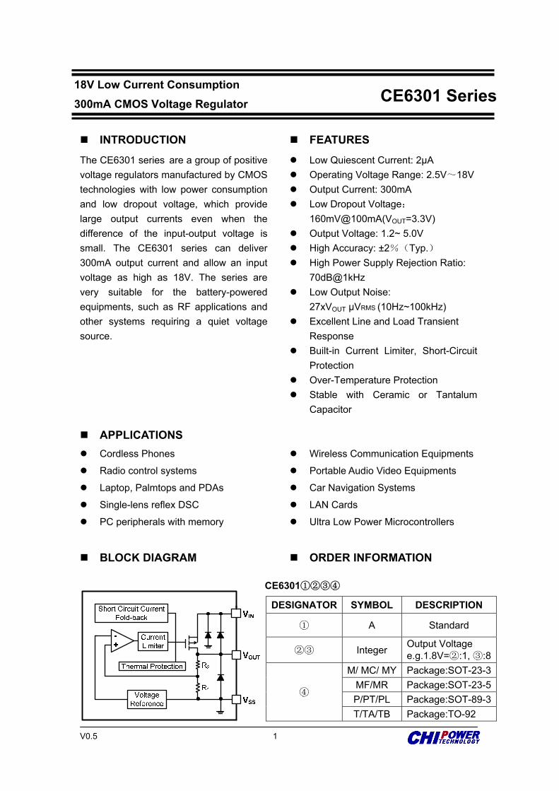
BLOCK DIAGRAM ORDER INFORMATION
DESIGNATOR SYMBOL DESCRIPTION
① A Standard
②③ Integer Output Voltage e.g.1.8V=②:1, ③:8
④
M/ MC/ MY Package:SOT-23-3MF/MR Package:SOT-23-5P/PT/PL Package:SOT-89-3T/TA/TB Package:TO-92
18V Low Current Consumption 300mA CMOS Voltage Regulator
CE6301 Series
V0.5 2
18V Low Current Consumption 300mA CMOS Voltage Regulator CE6301Series
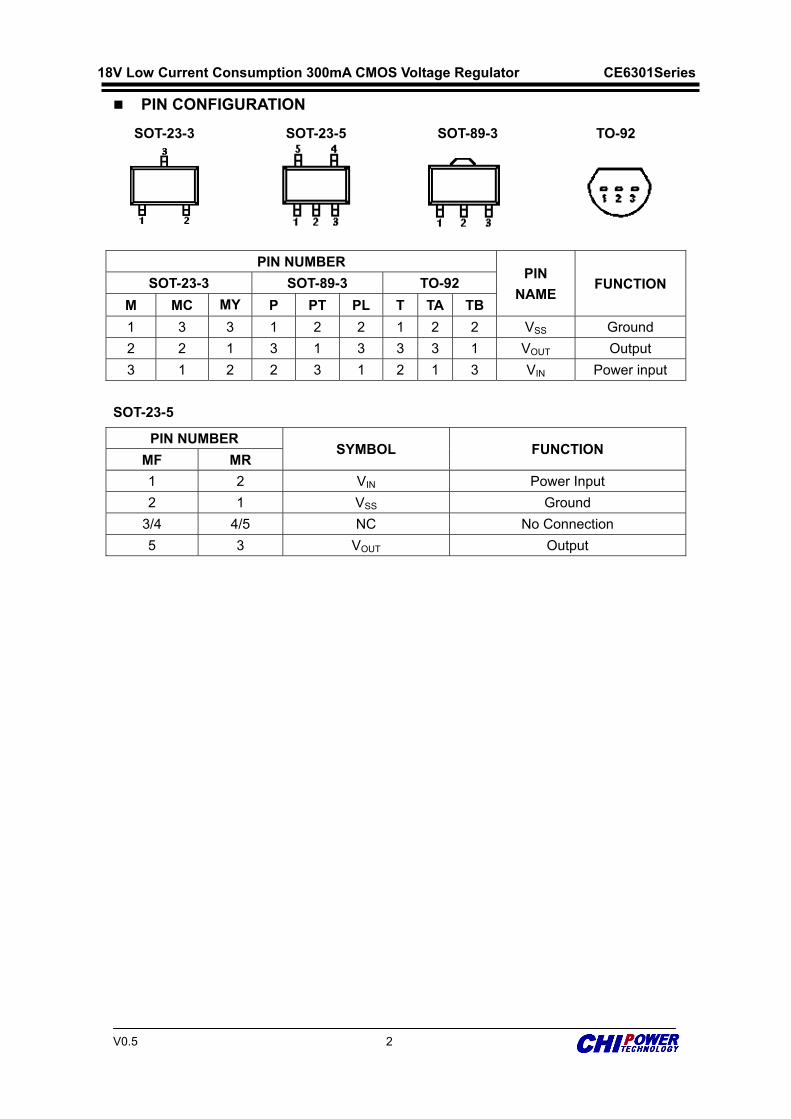
PIN CONFIGURATION
SOT-23-3 SOT-23-5 SOT-89-3 TO-92
PIN NUMBER PIN
NAME FUNCTION SOT-23-3 SOT-89-3 TO-92
M MC MY P PT PL T TA TB 1 3 3 1 2 2 1 2 2 VSS Ground 2 2 1 3 1 3 3 3 1 VOUT Output 3 1 2 2 3 1 2 1 3 VIN Power input
SOT-23-5
PIN NUMBER SYMBOL FUNCTION
MF MR 1 2 VIN Power Input 2 1 VSS Ground
3/4 4/5 NC No Connection 5 3 VOUT Output
V0.5 3
18V Low Current Consumption 300mA CMOS Voltage Regulator CE6301Series
ABSOLUTE MAXIMUM RATINGS(1) (Unless otherwise specified, TA=25°C)
PARAMETER SYMBOL RATINGS UNITSInput Voltage(2) VIN -0.3~24 V Output Voltage(2) VOUT -0.3~10 V Output Current IOUT 600 mA
Power Dissipation SOT-23
PD 0.4 W
SOT-89 0.6 W TO-92 0.6 W
Operating free air temperature range TA -40~85 °C Operating Junction Temperature Range(3) Tj -40~125 °C Storage Temperature Tstg -40~125 °C Lead Temperature(Soldering, 10 sec) Tsolder 260 °C
ESD rating(4) Human Body Model -(HBM) 8 kV
Machine Model- (MM) 400 V (1) Stresses beyond those listed under absolute maximum ratings may cause permanent damage to the
device. These are stress ratings only, and functional operation of the device at these or any other conditions
beyond those indicated under recommended operating conditions is not implied. Exposure to
absolute-maximum-rated conditions for extended periods my affect device reliability.
(2) All voltages are with respect to network ground terminal.
(3) This IC includes over temperature protection that is intended to protect the device during momentary
overload. Junction temperature will exceed 125°C when over temperature protection is active. Continuous
operation above the specified maximum operating junction temperature may impair device reliability.
(4) ESD testing is performed according to the respective JESD22 JEDEC standard.
The human body model is a 100 pF capacitor discharged through a 1.5kΩ resistor into each pin. The
machine model is a 200pF capacitor discharged directly into each pin.
RECOMMENDED OPERATING CONDITIONS
PARAMETER MIN. NOM. MAX. UNITS
Supply voltage at VIN 2.5 18 V Operating junction temperature range, Tj 0 125 °C Operating free air temperature range, TA 0 85 °C
V0.5 4
18V Low Current Consumption 300mA CMOS Voltage Regulator CE6301Series
ELECTRICAL CHARACTERISTICS CE6301 Series (VIN=VOUT+1V, CIN=COUT=1μF,TA=25 ,unless otherwise specified)
PARAMETER SYMBOL CONDITIONS MIN. TYP.(6) MAX. UNITSInput Voltage VIN 2.5 - 18 V
Output Voltage Range VOUT 1.2 - 5 V DC Output Accuracy IOUT=1mA -2 - 2 %
Dropout Voltage Vdif(7) IOUT =100mA,VOUT=3.3V - 160 - mV
Supply Current ISS IOUT=0A - 2 5 μA
Line Regulation ∆VOUT
VOUT ∆VIN
IOUT =10mA VOUT +1V≤VIN≤18V
- 0.01 0.3 %/V
Load Regulation ∆VOUT VIN= VOUT +1V,
1mA≤IOUT≤100mA - 10 - mV
Temperature Coefficient
∆VOUTVOUT ∆TA
IOUT=10mA,
-40°C<TA<125°C 50 ppm
Output Current Limit ILIM VOUT= 0.5 x VOUT(Normal) , VIN = 5V
350 450 550 mA
Short Current ISHORT VOUT =VSS - 40 - mA
Power Supply Rejection Ratio
PSRR IOUT=50mA
100Hz 80
dB 1kHz - 70 - 10kHz - 60 -
100kHz - 40 -
Output Noise Voltage VON BW=10Hz to 100kHz - 27 x VOUT - μVRMS
Thermal Shutdown Temperature TSD —— - 150 - °C
Thermal Shutdown Hysteresis TSD —— - 20 - °C
(6) Typical numbers are at 25°C and represent the most likely norm.
(7) Vdif:The Difference Of Output Voltage And Input Voltage When Input Voltage Is Decreased Gradually
Till Output Voltage Equals To 98% Of VOUT (E).
TYPICAL APPLICATION CIRCUIT
V0.5 5
18V Low Current Consumption 300mA CMOS Voltage Regulator CE6301Series
APPLICATION INFORMATION Selection of Input/ Output Capacitors
In general, all the capacitors need to be low leakage. Any leakage the capacitors have will
reduce efficiency, increase the quiescent current. A recent trend in the design of portable devices has been to use ceramic capacitors to filter
DC/DC converter inputs. Ceramic capacitors are often chosen because of their small size,
low equivalent series resistance (ESR) and high RMS current capability. Also, recently,
designers have been looking to ceramic capacitors due to shortages of tantalum capacitors. Unfortunately, using ceramic capacitors for input filtering can cause problems. Applying a
voltage step to a ceramic capacitor causes a large current surge that stores energy in the
inductances of the power leads. A large voltage spike is created when the stored energy is
transferred from these inductances into the ceramic capacitor. These voltage spikes can
easily be twice the amplitude of the input voltage step. (See “Ceramic Input Capacitors Can
Cause Overvoltage Transients”——Linear Technology application note 88, March 2001) Many types of capacitors can be used for input bypassing, however, caution must be
exercised when using multilayer ceramic capacitors (MLCC). Because of the self-resonant
and high Q characteristics of some types of ceramic capacitors, high voltage transients can
be generated under some start-up conditions, such as connecting the LDO input to a live
power source. Adding a 3Ω resistor in series with an X5R ceramic capacitor will minimize
start-up voltage transients. The LDO also requires an output capacitor for loop stability. Connect a 1μF tantalum
capacitor from OUT to GND close to the pins. For improved transient response, this output
capacitor may be ceramic.
V0.5 6
18V Low Current Consumption 300mA CMOS Voltage Regulator CE6301Series
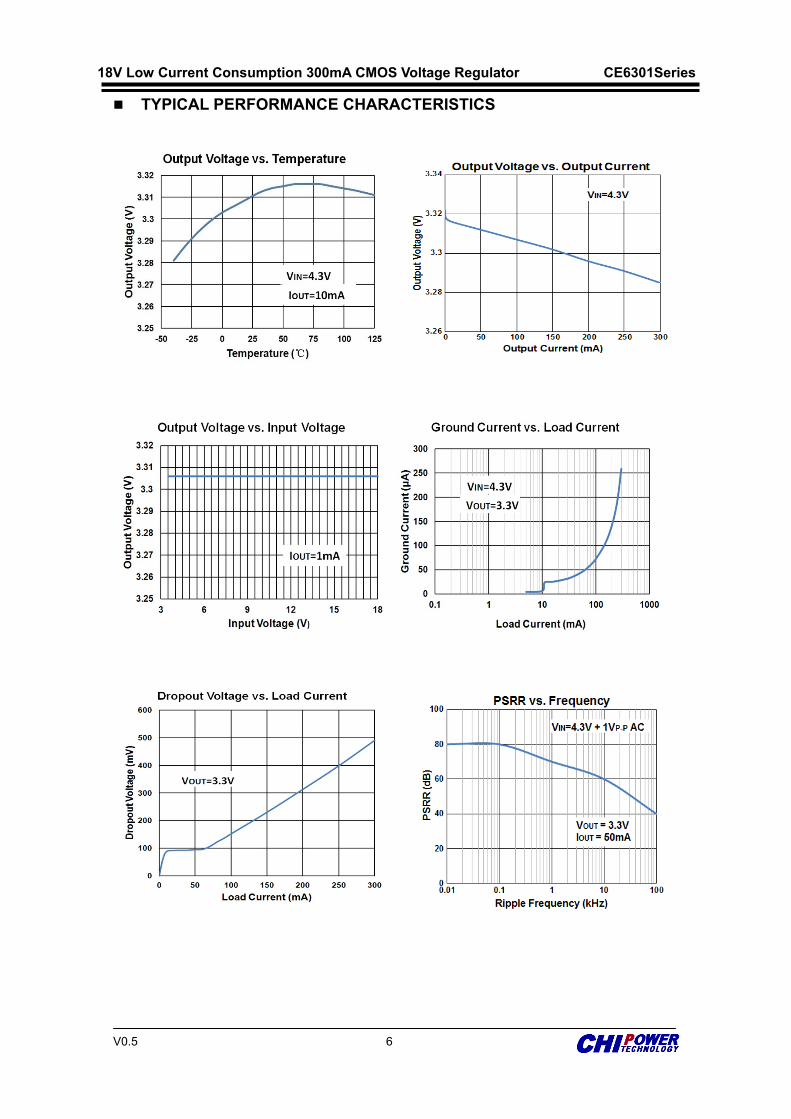
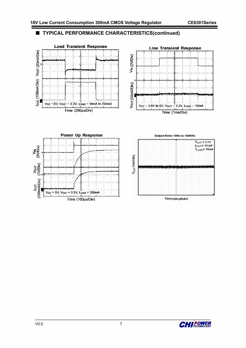
TYPICAL PERFORMANCE CHARACTERISTICS
V0.5
18V Lo
T
w Current C
TYPICAL P
Consumptio
PERFORM
on 300mA C
MANCE CH
7
CMOS Volta
HARACTE
age Regula
RISTICS(c
tor
continued
CE630
d)
01Series
V0.5 8
18V Low Current Consumption 300mA CMOS Voltage Regulator CE6301Series
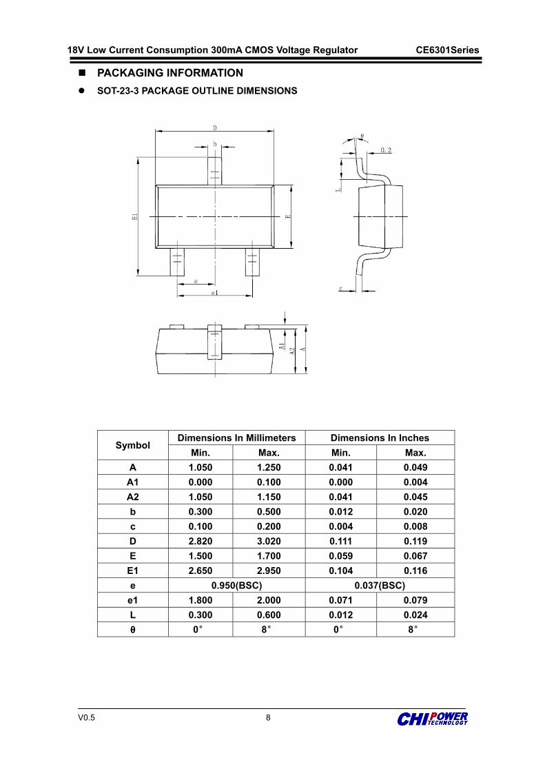
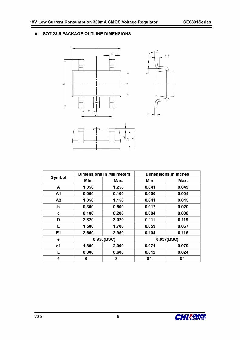
PACKAGING INFORMATION SOT-23-3 PACKAGE OUTLINE DIMENSIONS
Symbol Dimensions In Millimeters Dimensions In Inches
Min. Max. Min. Max. A 1.050 1.250 0.041 0.049
A1 0.000 0.100 0.000 0.004 A2 1.050 1.150 0.041 0.045 b 0.300 0.500 0.012 0.020 c 0.100 0.200 0.004 0.008 D 2.820 3.020 0.111 0.119 E 1.500 1.700 0.059 0.067
E1 2.650 2.950 0.104 0.116 e 0.950(BSC) 0.037(BSC)
e1 1.800 2.000 0.071 0.079 L 0.300 0.600 0.012 0.024 θ 0° 8° 0° 8°
V0.5 9
18V Low Current Consumption 300mA CMOS Voltage Regulator CE6301Series
SOT-23-5 PACKAGE OUTLINE DIMENSIONS
Symbol Dimensions In Millimeters Dimensions In Inches
Min. Max. Min. Max. A 1.050 1.250 0.041 0.049
A1 0.000 0.100 0.000 0.004 A2 1.050 1.150 0.041 0.045 b 0.300 0.500 0.012 0.020 c 0.100 0.200 0.004 0.008 D 2.820 3.020 0.111 0.119 E 1.500 1.700 0.059 0.067
E1 2.650 2.950 0.104 0.116 e 0.950(BSC) 0.037(BSC)
e1 1.800 2.000 0.071 0.079 L 0.300 0.600 0.012 0.024 θ 0° 8° 0° 8°
V0.5
18V Lo
S
w Current C
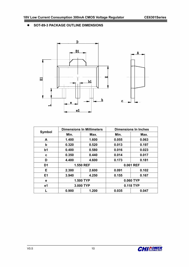
SOT-89-3 PA
Symbo
A b
b1 c D
D1 E
E1 e
e1 L
Consumptio
ACKAGE O
l Dime
M1.40.30.40.34.4
2.33.9
0.9
on 300mA C
OUTLINE DI
ensions In Min.
400 320 400 350 400
1.550 R300 940
1.500 T3.000 T
900
10
CMOS Volta
MENSIONS
MillimetersMax. 1.600 0.520 0.580 0.440 4.600
REF 2.600 4.250
TYP TYP
1.200
age Regula
S
s DimMin0.050.010.010.010.17
0.090.15
0.03
tor
mensions Inn. 55 13 16 14 73
0.061 RE91 55
0.060 TY0.118 TY
35
CE630
n Inches Max. 0.063 0.197 0.023 0.017 0.181
EF 0.102 0.167
YP YP
0.047
01Series
V0.5
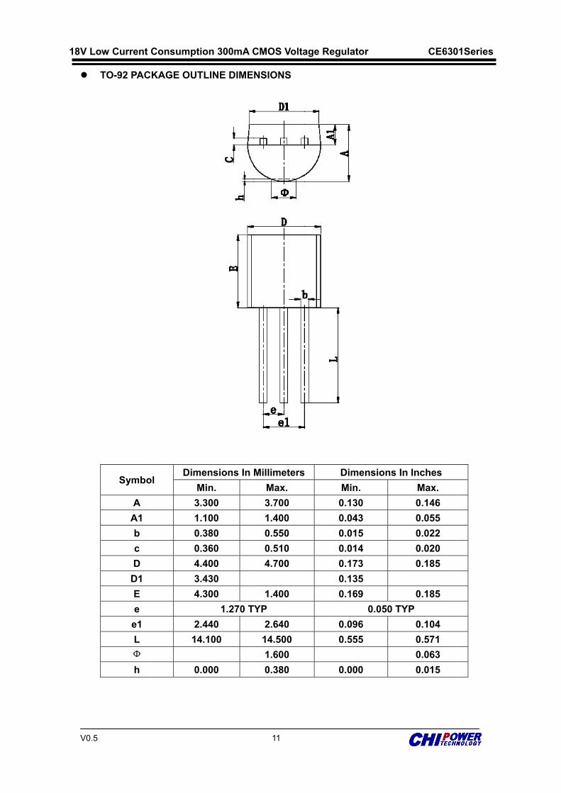
18V Lo
T
w Current C
TO-92 PACK
Symbo
A A1 b c D
D1 E e
e1 L Ф h
Consumptio
KAGE OUT
l Dime
M3.31.0.30.34.43.44.3
2.414
0.0
on 300mA C
TLINE DIME
ensions In Min.
300 100 380 360 400 430 300
1.270 T440 .100
000
11
CMOS Volta
NSIONS
MillimetersMax. 3.700 1.400 0.550 0.510 4.700
1.400
TYP 2.640
14.500 1.600 0.380
age Regula
s DimMin0.130.040.010.010.170.130.16
0.090.55
0.00
tor
mensions Inn. 30 43 15 14 73 35 69
0.050 TY96 55
00
CE630
n Inches Max. 0.146 0.055 0.022 0.020 0.185
0.185
YP 0.104 0.571 0.063 0.015
01Series
V0.5 12
18V Low Current Consumption 300mA CMOS Voltage Regulator CE6301Series
© Nanjing Chipower Electronics Inc. Chipower cannot assume responsibility for use of any circuitry other than circuitry entirely embodied in a Chipower product. No circuit patent license, copyrights or other intellectual property rights are implied. Chipower reserves the right to make changes to their products or specifications without notice. Customers are advised to obtain the latest version of relevant information to verify, before placing orders, that information being relied on is current and complete.