(19) tzz zz¥ t - epo
TRANSCRIPT

Note: Within nine months of the publication of the mention of the grant of the European patent in the European PatentBulletin, any person may give notice to the European Patent Office of opposition to that patent, in accordance with theImplementing Regulations. Notice of opposition shall not be deemed to have been filed until the opposition fee has beenpaid. (Art. 99(1) European Patent Convention).
Printed by Jouve, 75001 PARIS (FR)
(19)E
P1
652
003
B1
TEPZZ_65 ZZ¥B_T(11) EP 1 652 003 B1
(12) EUROPEAN PATENT SPECIFICATION
(45) Date of publication and mention of the grant of the patent: 07.01.2015 Bulletin 2015/02
(21) Application number: 04754129.7
(22) Date of filing: 02.06.2004
(51) Int Cl.:G03F 7/20 (2006.01)
(86) International application number: PCT/US2004/017452
(87) International publication number: WO 2005/010611 (03.02.2005 Gazette 2005/05)
(54) WAFER TABLE FOR IMMERSION LITHOGRAPHY
WAFER-TISCH FÜR DIE IMMERSIONS-LITHOGRAPHIE
TABLE PORTE-PLAQUETTES POUR LITHOGRAPHIE PAR IMMERSION
(84) Designated Contracting States: AT BE BG CH CY CZ DE DK EE ES FI FR GB GR HU IE IT LI LU MC NL PL PT RO SE SI SK TR
(30) Priority: 08.07.2003 US 485868 P
(43) Date of publication of application: 03.05.2006 Bulletin 2006/18
(60) Divisional application: 12159430.3 / 2 466 38212159431.1 / 2 466 38314189351.114189363.6
(73) Proprietor: NIKON CORPORATIONChiyoda-kuTokyo 100-8331 (JP)
(72) Inventors: • HAZELTON, Andrew, J.
Chiyoda-ku, 100-8331 Tokyo (JP)
• TAKAIWA, HiroakiChiyoda-ku, 100-8331 Tokyo (JP)
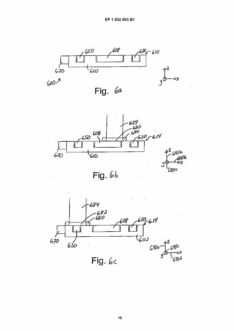
(74) Representative: Hoffmann EitlePatent- und Rechtsanwälte PartmbB Arabellastraße 3081925 München (DE)
(56) References cited: EP-A- 1 429 188 EP-A- 1 486 828WO-A-2004/090577 US-A- 5 825 043US-A- 6 078 380
• OWA S ET AL: "Immersion lithography" PROCEEDINGS OF THE SPIE, SPIE, BELLINGHAM, VA, US, vol. 5040, no. 1, 28 February 2003 (2003-02-28), pages 724-733, XP002294500 ISSN: 0277-786X
EP 1 652 003 B1
2
5
10
15
20
25
30
35
40
45
50
55
Description
REFERENCE TO RELATED APPLICATION
[0001] This application claims priority to U.S. Provi-sional Patent Application No. 60/485,868, filed July 8,2003.
BACKGROUND OF THE INVENTION
1. Field of Invention
[0002] The present invention relates generally to sem-iconductor processing equipment. More particularly, thepresent invention relates to a method and an apparatusfor enabling liquid in an immersion lithography system toeffectively be contained between a surface of a lens anda plane that is moved relative to the lens.
2. Description of the Related Art
[0003] For precision instruments such as photolithog-raphy machines which are used in semiconductorprocessing, factors which affect the performance, e.g.,accuracy, of the precision instrument generally must bedealt with and, insofar as possible, eliminated. When theperformance of a precision instrument such as an immer-sion lithograph exposure system is adversely affected,products formed using the precision instrument may beimproperly formed and, hence, function improperly.[0004] In an immersion lithography system, a liquid isprovided between a lens and the surface of a wafer inorder to improve the imaging performance of the lens.The use of liquid allows a numerical aperture associatedwith the lens, i.e., an effective numerical aperture of thelens, to essentially be increased substantially without al-tering characteristics of the lens, since a liquid such aswater generally has a refractive index that is greater thanone. In general, a higher numerical aperture enables asharper image to be formed on the wafer. As will be ap-preciated by those skilled in the art, a high refractive indexliquid allows for a high numerical aperture of the lenssince an effective numerical aperture of a lens system ofan immersion lithography system is generally defined tobe approximately equal to the sine of an angle of diffrac-tion of light which passes through a lens and reflects offa surface multiplied by the refractive index of the liquid.Since the refractive index of the liquid is greater than one,the use of liquid allows the effective numerical apertureof the lens to be increased, thereby enabling the resolu-tion associated with the lens to essentially be improved.[0005] Within most conventional lithography systems,air is present between a lens and a surface which passesunder the lens, e.g., the surface of a wafer. In such sys-tems, the numerical aperture associated with the lens isoften in the range of approximately 0.8 to 0.9. Increasingthe numerical aperture of a lens to achieve an improvedresolution is generally impractical, as the diameter of a
lens generally must be increased, which adds significantdifficulty to a lens manufacturing process. In addition, thenumerical aperture of a lens in air is theoretically limitedto one, and, in practice, is limited to being somewhat lessthan one. Hence, immersion lithography systems enablethe effective numerical aperture of a lens to be increasedsubstantially beyond what is possible with a lens in air.[0006] Fig. 1 is a diagrammatic cross-sectional repre-sentation of a portion of an immersion lithography appa-ratus. An immersion lithography apparatus 100 includesa lens assembly 104 which is positioned over a wafertable 112 which supports a wafer 108. Wafer table 112is arranged to be scanned or otherwise moved underlens assembly 104. A liquid 116, which may be water ina typical application which uses approximately 193 na-nometers (nm) of radiation, is present in a gap betweenlens assembly 104 and wafer 108. In order to effectivelyprevent liquid 116 from leaking out from under lens as-sembly 104, i.e., to effectively laterally contain liquid 116between lens assembly 104 and wafer 108, a retainingring 120 may be positioned such that retaining ring 120enables liquid 116 to remain between lens assembly 104and wafer 108, and within an area defined by retainingring 120.[0007] While retaining ring 120 is generally effective incontaining liquid 116 when lens assembly 104 is posi-tioned such that a small gap between retaining ring 120and a surface of wafer 108 is maintained, for a situationin which at least a part of retaining ring 120 is above wafer108, liquid 116 may leak out from between lens assembly104 and wafer 108. By way of example, when an edgeof wafer 108 is to be patterned, lens assembly 104 maybe substantially centered over the edge such that a por-tion of retaining ring 120 fails to maintain the small gapunder the bottom surface of retaining ring 120, and liquid116 is allowed to leak out from between lens assembly104 and wafer 108. As shown in Fig. 2, when lens as-sembly 104 is positioned such that at least part of a bot-tom surface of retaining ring 120 is not in contact withwafer 108, liquid 116 may not be contained in an areadefined by retaining ring 120 between lens assembly 104and wafer 108.[0008] In an immersion lithography apparatus, a wafertable may support sensors and other components, e.g.,a reference flat that is used to calibrate automatic focus-ing operations. Such sensors and other components gen-erally may be positioned beneath a lens at some point.That is, sensors and other components associated witha wafer table may be occasionally positioned beneath alens during the course of operating the lens and the wafertable. While the use of a retaining ring may prevent liquidfrom leaking out of a gap between a lens assembly andthe top surface of the wafer, liquid may leak out frombetween the lens assembly and top surfaces of sensorsand other components when the lens assembly is posi-tioned over the sensors or other components.[0009] Fig. 3 is a block diagram representation of awafer table which supports a sensor and a wafer holder
1 2
EP 1 652 003 B1
3
5
10
15
20
25
30
35
40
45
50
55
that holds a wafer. A wafer table 312 supports a waferholder 310 which is arranged to hold a wafer (not shown),a sensor 350, and an interferometer mirror 352. Sensor350 may be used through a lens (not shown) with liquid(not shown) between the lens and sensor 350. However,liquid will often flow out of the gap between a lens (notshown) and sensor 350 particularly when an edge of sen-sor 350 is positioned substantially beneath a center ofthe lens. The effectiveness of sensor 350 may be com-promised when sensor 350 is designed and calibratedto operate in a liquid, and there is insufficient liquidpresent between a lens (not shown) and sensor 350. Fur-ther, when liquid (not shown) flows out of the gap betweena lens (not shown) and sensor 350, the liquid whichflowed out of the gap is effectively lost such that whenthe lens is subsequently positioned over a wafer (notshown) supported by wafer holder 310, the amount ofliquid between the lens and the wafer may not be suffi-cient to enable the effective numerical aperture of thelens to be as high as desired. Hence, when liquid is notsuccessfully contained between a lens (not shown) andsensor 350 while sensor 350 is at least partially posi-tioned under the lens, an overall lithography processwhich involves the lens and sensor 350 may be compro-mised.[0010] Therefore, what is needed is a method and anapparatus for allowing liquid to be maintained in a rela-tively small gap defined between a surface of a lens anda surface of substantially any sensors or componentswhich are supported by a wafer table. That is, what isdesired is a system which is suitable for preventing liquidwhich is positioned between a lens and substantially anysurface on a wafer table which is moved under the lensfrom leaking out from between the lens and the surface.[0011] US 5,825,043 A discloses a lithography appa-ratus having a wafer holder and an auxiliary plate, inwhich, if the difference between the height of the surfaceof the wafer placed on the wafer holder and the heightof the surface of the auxiliary plate in the Z-direction islarger than an allowable difference, a Z-drive unit is usedto correct the height of the surface of the auxiliary plateso that the difference is reduced to a value smaller thanthe allowable value.[0012] EP 1 429 188 A2 and WO 2004/090577 A2 eachrelate to immersion lithographic apparatus. These latterdocuments, being published before the earliest claimedpriority date for the present disclosure, are not relevantfor the determination of obviousness of the claimed sub-ject-matter.
SUMMARY OF THE INVENTION
[0013] The present invention relates an immersion li-thography exposure apparatus. According to one aspectof the present invention, there is provided an immersionlithography exposure apparatus as recited in claim 1 be-low. Dependent claims therefrom are directed to partic-ular embodiments thereof.
[0014] According to another aspect of the present in-vention, there is provided an immersion lithography ex-posure method as recited in claim 12 below. Dependentclaims therefrom are directed to particular embodimentsthereof.[0015] In one embodiment, the sensor may be at leastone of an aerial image sensor, a dose sensor, and a doseuniformity sensor. In another embodiment, the wafer ta-ble assembly is arranged to support a wafer holder thatholds the wafer such that the top surface of the wafer isat substantially the same height as the top surface of thewafer table assembly.[0016] A wafer table arrangement which is configuredto enable surfaces which are to viewed through a lens toform a relatively planar overall surface of substantiallythe same height facilitates an immersion lithographyprocess. When substantially all elements carried on awafer table have top surfaces that are substantially levelwith the top surface of the wafer table, and any gapsbetween the sides of the components and the sides ofopenings in the wafer table are relatively small, the overalltop surface of a wafer table arrangement may traverseunder a lens while a layer or a film of liquid is effectivelymaintained between a surface of the lens and the overalltop surface. Hence, an immersion lithography processmay be performed substantially without the integrity ofthe layer of liquid between the surface of the lens andthe overall top surface of the wafer table arrangementbeing compromised by the loss of liquid from the layerof liquid between the surface of the lens and the overalltop surface of the wafer table arrangement.[0017] In some embodiments of the present invention,the apparatus includes a lens which has a first surfaceand an associated effective numerical aperture. The ap-paratus also includes a liquid that is suitable for enhanc-ing the effective numerical aperture of the lens, and atable arrangement. The table arrangement has a sub-stantially flat top surface that opposes the first surface,and the liquid is arranged substantially between the sub-stantially flat top surface and the first surface. The sub-stantially flat top surface includes a top surface of anobject to be scanned and a top surface of at least onesensor.[0018] These and other advantages of the present in-vention will become apparent upon reading the followingdetailed descriptions and studying the various figures ofthe drawings.
BRIEF DESCRIPTION OF THE DRAWINGS
[0019] The invention may best be understood by ref-erence to the following description taken in conjunctionwith the accompanying drawings in which:
Fig. 1 is a diagrammatic cross-sectional representa-tion of a portion of an immersion lithography appa-ratus in a first orientation.Fig. 2 is a diagrammatic representation cross-sec-
3 4
EP 1 652 003 B1
4
5
10
15
20
25
30
35
40
45
50
55
tional representation of a portion of an immersionlithography apparatus, i.e., apparatus 100 of Fig. 1,in a second orientation.Fig. 3 is a block diagram representation of a wafertable which supports a sensor and a wafer holderthat holds a wafer.Fig. 4 is a block diagram representation of a top viewof a wafer table assembly in accordance with an em-bodiment of the present invention.Fig. 5 is a block diagram representation of a top viewof components which are supported by a wafer tableassembly with a substantially uniform, planar overalltop surface in accordance with an embodiment ofthe present invention.Fig. 6a is a diagrammatic cross-sectional represen-tation of a wafer table assembly which has a sub-stantially uniform, planar overall top surface in ac-cordance with an embodiment of the present inven-tion.Fig. 6b is a diagrammatic representation of a wafertable assembly, e.g., wafer table assembly 600 ofFig. 6a, with a lens assembly positioned over a waferholder in accordance with an embodiment of thepresent invention.Fig. 6c is a diagrammatic representation of a wafertable assembly, e.g., wafer table assembly 600 ofFig. 6a, with a lens assembly positioned over a com-ponent in accordance with an embodiment of thepresent invention.Fig. 7 is a diagrammatic representation of a photo-lithography apparatus in accordance with an embod-iment of the present invention.Fig. 8 is a process flow diagram which illustrates thesteps associated with fabricating a semiconductordevice in accordance with an embodiment of thepresent invention.Fig. 9 is a process flow diagram which illustrates thesteps associated with processing a wafer, i.e., step1304 of Fig. 4, in accordance with an embodimentof the present invention.Fig. 10a is a diagrammatic representation of a wafertable surface plate and a wafer table in accordancewith an embodiment of the present invention.Fig. 10b is a diagrammatic cross-sectional represen-tation of wafer table assembly which includes a wafertable and a wafer table surface plate in accordancewith an embodiment of the present invention.Fig. 11 a is a diagrammatic cross-sectional repre-sentation of a wafer table and a wafer table surfaceplate with windows in accordance with an embodi-ment of the present invention.Fig. 11b is a diagrammatic cross-sectional represen-tation of wafer table assembly which includes a wafertable and a wafer table surface plate with windows,i.e., wafer table 904 and wafer table surface plate908 of Fig. 11a, in accordance with an embodimentof the present invention.
DETAILED DESCRIPTION OF THE EMBODIMENTS
[0020] In immersion lithography systems, a wafer sur-face must generally be viewed through a lens with a layerof liquid such as a relatively thin film of liquid betweenthe lens and the wafer surface. Some components suchas sensors and/or reference members may often beviewed through the lens with a layer of liquid betweenthe lens and the surfaces of the components. Maintainingthe layer of liquid in a gap between the lens and the sur-face of the wafer, even when the lens is arranged to viewedge portions of the wafer, allows the immersion lithog-raphy system to operate substantially as desired. Simi-larly, maintaining the layer of liquid in a gap between thelens and the surface of components such as sensorsand/or reference members also facilitates the efficientoperation of the immersion lithography system.[0021] By utilizing a wafer table arrangement which isconfigured to enable surfaces which are to viewedthrough a lens and a top surface of the wafer table ar-rangement to form a relatively planar, substantially uni-form overall surface. When substantially all componentsassociated with the wafer table arrangement have a sur-face which is substantially level with the top surface of awafer and the top surface of a wafer table, and any gapsbetween the sides of the components and the sides ofopenings in the wafer table are relatively small, the overalltop surface of the wafer table arrangement may traverseunder a lens while a layer or a film of liquid is effectivelymaintained between a surface of the lens and the overalltop surface. As a result, an immersion lithography proc-ess may be performed substantially without having theintegrity of the layer of liquid, i.e., the layer of liquid be-tween the surface of the lens and the overall top surfaceof the wafer table arrangement, compromised.[0022] A wafer table which has a substantially raised,flat top surface of a uniform height allows a wafer andother components, e.g., sensors, to be installed such thata flat surface of the wafer and flat surfaces of the com-ponents are at substantially the same level or height asthe raised, flat top surface of the wafer table. In one em-bodiment, an overall wafer table assembly includesopenings within which a wafer, or a wafer holder on whichthe wafer is supported, and sensors may be positioned.Fig. 4 is a block diagram representation of a top view ofa wafer table assembly in accordance with an embodi-ment of the present invention. A wafer table assembly402 includes openings 409, 452 which are sized to ef-fectively house a wafer 408 and components 450, re-spectively, such that top surfaces of wafer 408 and com-ponents 450 are at substantially the same level as a topsurface 414 of wafer table assembly 402. Typically, open-ings 409,452 are sized to accommodate wafer 408 andcomponents 450, respectively, such that a spacing be-tween the outer edges or wafer 408 or components 450and their respective openings 409, 452 is relatively small,e.g., between approximately ten and approximately 500micrometers.
5 6

EP 1 652 003 B1
5
5
10
15
20
25
30
35
40
45
50
55
[0023] In general, the spacing between wafer 408, orin some cases, a wafer holder (not shown) and opening409, as well as the spacing between components 450and their corresponding openings 452 does not signifi-cantly affect the overall planar quality of an overall topsurface of wafer table assembly 402. That is, an overalltop surface of wafer table assembly 402 which includestop surface 414, the top surface of wafer 408, and thetop surfaces of components 450 is substantially planar,with the planarity of the overall top surface being sub-stantially unaffected by the presence of the small gapsbetween the sides of wafer 408 and opening 409, andthe sides of components 450 and openings 452.[0024] Components 450 may include, but are not lim-ited to, various sensors and reference marks. With ref-erence to Fig. 5, components which are supported by awafer table assembly with a substantially uniform, planaroverall top surface will be described in accordance withan embodiment of the present invention. A wafer tableassembly 502 includes a raised, substantially uniformtop surface 514 in which openings 509, 552 are defined.Opening 509 is arranged to hold a wafer 508 which maybe supported by a wafer holder (not shown). Openings552 are arranged to support any number of components.In the described embodiment, openings 552 are ar-ranged to support a dose sensor or a dose uniformitysensor 556, an aerial image sensor 558, a reference flat560, and a fiducial mark 562, which each have top sur-faces that are arranged to be of substantially the sameheight as top surface 514 such that an overall, substan-tially uniform, planar top surface is formed. Examples ofa suitable dose sensor or dose uniformity sensor 556 aredescribed in U.S. Patent No. 4,465,368, U.S. Patent No.6,078,380, and U.S. Patent Publication No.2002/0061469A1, which are each hereby referred to. Anexample of an aerial image sensor 558 is described inU.S. Patent Publication No. 2002/0041377A1, which ishereby referred to. An example of a reference flat 560 isdescribed in U.S. Patent No. 5,985,495, which is herebyreferred to, while an example of a fiducial mark 562 isdescribed in U.S. Patent No. 5,243,195, which is herebyreferred to.[0025] It should be appreciated that openings 552 aresized to accommodate components such that gaps be-tween the sides of components, as for example dosesensor or dose uniformity sensor 556, aerial image sen-sor 558, reference flat 560, and fiducial mark 562, andedges of openings 552 are not large enough to signifi-cantly affect the uniformity and planarity of the overalltop surface. In other words, components are relativelytightly fit within openings 552.[0026] Dose sensor or a dose uniformity sensor 556,one or both of which may be included in openings 552,is arranged to be used to determine a strength of a lightsource associated with a lens assembly (not shown) bystudying light energy at the level of the top surface ofwafer 508. In one embodiment, only a dose uniformitysensor is typically included. A dose sensor generally
measures absolute illumination intensity, while a doseuniformity sensor typically measures variations over anarea. As such, dose sensor or does uniformity sensor556 is positioned in the same plane as the top surfaceof wafer 508. Aerial image sensor 558 is arranged toeffectively measure an aerial image that is to be projectedonto the surface of wafer 508 and, hence, exposed onphotoresist. In order for aerial image sensor to accuratelymeasure an aerial image, aerial image sensor 558 is es-sentially positioned at the same level or plane as the topsurface of wafer 508.[0027] Reference flat 560 is generally used to calibratethe automatic focus functionality of a lens assembly (notshown), while fiducial mark 562 is a pattern that is usedto enable wafer 508 to be aligned with respect to the lensassembly and reticle, as will be understood by thoseskilled in the art. Both reference flat 560 and fiducial mark562 are positioned in the same plane as wafer 508.[0028] Fig. 6a is a diagrammatic cross-sectional rep-resentation of a wafer table assembly which has a sub-stantially uniform, planar overall top surface in accord-ance with an embodiment of the present invention. Anoverall wafer table assembly 600 includes a wafer table602 which is arranged to support a wafer holder 608 thatholds a wafer (not shown) such that a top surface of thewafer is substantially flush with an overall top surface614 of wafer table assembly 600. Wafer table 602 alsosupports components 650, 8 which may include sensorsand reference marks, such that top surfaces of compo-nents 650 are also substantially flush with overall topsurface 614, as discussed above. In other words, topsurfaces of components 650, wafer holder 608 when sup-porting a wafer (not shown), and wafer table 602 effec-tively form a substantially flat overall top surface 614 ofrelatively uniform height Wafer holder 608 and compo-nents 650 are arranged to be relatively tightly fit into open-ings defined within wafer table 602 such that a gap be-tween the side of wafer holder 608 and the sides of anassociated opening within wafer table 602, as well asgaps between components 650 and the sides of associ-ated openings within wafer table 602, are each relativelysmall, and do not have a significant effect on the uniform-ity of overall top surface 614.[0029] Wafer table 602 may supports additional com-ponents or elements in addition to wafer holder 608, awafer (not shown), and components 650. By way of ex-ample, wafer table 602 may support an interferometermirror 670. It should be appreciated that a top surface ofinterferometer mirror 602 may also be substantially levelwith overall top surface 614. Hence, in one embodiment,overall top surface 614 may include interferometer mirror670.[0030] Overall top surface 614 enables liquid to bemaintained in a gap between a lens assembly and overalltop surface 614 when a component 650 or wafer holder608 traverses beneath the lens. Fig. 6b is a diagrammaticrepresentation of a wafer table assembly, e.g., wafer ta-ble assembly 600 of Fig. 6a, which is arranged to scan
7 8

EP 1 652 003 B1
6
5
10
15
20
25
30
35
40
45
50
55
beneath a lens assembly in accordance with an embod-iment of the present invention. A lens assembly 684,which is arranged to be positioned over overall top sur-face 614 is effectively separated from overall top surface614 along a z-axis 690a by a layer of liquid 682. The sizeof the immersion area covered by liquid 682 is relativelysmall, e.g., the size of the immersion area may be smallerthan that of the wafer (not shown). Local fill methodswhich are used to provide the liquid of the immersionarea are described in co-pending PCT International Pat-ent Application No. PCT/US04/10055 (filed March 29,2004), co-pending PCT International Patent ApplicationNo. PCT/US04/09994 (filed April 1, 2004), and co-pend-ing PCT International Patent Application No.PCT/US04/10071 (filed April 1, 2004), which are eachhereby referred to. Layer of liquid 682 is effectively heldbetween overall top surface 614 and lens assembly 684with respect to an x-axis 690b and a γ-axis 690c by aretaining ring 680, although substantially any suitable ar-rangement may be used to effectively hold layer of liquid682 in place relative to x-axis 690b and γ-axis 690c. Re-taining ring 680 is arranged as a ring-like structure withrespect to x-axis 690b and γ-axis 690c which containsliquid 682 in an area defined by the edges of retainingring 680. That is, retaining ring 680 forms a ring-likeshape about z-axis 690a.[0031] In another embodiment, retaining ring 680 maynot be necessary. If the gap between lens assembly 684and overall top surface 614 (or wafer surface) is relativelysmall, e.g., between approximately 0.5 mm and approx-imately 5 mm, layer of liquid 682 may be effectively heldbetween the gap with surface tension of liquid 682.[0032] In general, liquid 682 may be substantially anysuitable liquid which fills a gap or a space between asurface of lens assembly 684 and overall top surface 614within an area defined by retaining ring 680 that allowsan effective numerical aperture of a lens included in lensassembly 684 to be increased for the same wavelengthof light and the same physical size of the lens. Liquidsincluding various oils, e.g., Fomblin™ oil, may be suitablefor use as liquid 682. In one embodiment, as for examplewithin an overall system which uses approximately193nanometers (nm) of radiation, liquid 682 is water. How-ever, for shorter wavelengths, liquid 682 may be an oil.[0033] Since overall top surface 614 is substantiallyflat and uniform, when lens assembly 684 is positionedover wafer holder 608, liquid 682 does not leak out frombetween overall top surface 614 and lens assembly 684,since retaining ring 680 remains in contact or in closeproximity with overall top surface 614, even when lensassembly 684 is positioned over an edge of wafer holder608. The uniformity and planarity of overall top surface614 also allows liquid 682 to remain between lens as-sembly 684 and overall top surface 614 when lens as-sembly 684 is oriented over a component 650, as shownin Fig. 6c.[0034] While a wafer table arrangement may includea wafer table in which openings have been defined to
house a wafer or a wafer holder and any number of com-ponents, a wafer table arrangement may instead includea wafer table which has no openings to house a wafer ora wafer holder and any number of components and struc-tures which may cooperate with the wafer table to effec-tively form openings in which a wafer or a wafer holderand any number of components may be placed. In otherwords, a substantially planar wafer table arrangementmay either include openings formed within a wafer tableas discussed above, or openings defined by a structureor structures positioned atop a wafer table.[0035] When a wafer table arrangement includes astructure that defines openings which may effectivelyhouse a wafer and components and provides a substan-tially planar top surface for the wafer table arrangement,the structure may generally be a plate-like structure with-in which openings are formed. With reference to Fig. 10a,a wafer table arrangement which includes a wafer tableand a wafer table surface plate will be described in ac-cordance with an embodiment of the present invention.A wafer table arrangement 700 includes a wafer table704 and a wafer table surface plate 708, Wafer table 704supports a wafer 712 and one or more components 716which may include various sensors, a fiducial mark, or areference flat. Wafer table surface plate 708, which maybe formed from any suitable material, e.g., Teflon, in-cludes an opening 720 within which wafer 712, may bepositioned when wafer table surface plate 708 is posi-tioned atop wafer table 704. Openings 724, which arealso defined in wafer table surface plate 708, are ar-ranged to fit around components 716 when wafer tablesurface plate 708 is positioned atop wafer table 704.[0036] Wafer table surface plate 708 includes a topsurface which, when wafer table surface plate 708 is po-sitioned atop wafer table 704 such that wafer 712 is po-sitioned within opening 720 and components 716 are po-sitioned within openings 724, cooperates with a top sur-face of wafer 712 and top surfaces of components 716to create a substantially uniform, planar overall top sur-face. As shown in Fig. 10b, when a wafer table surfaceplate 808 is positioned over a wafer table 804, a top sur-face of components 816, e.g., sensors, and a top surfaceof a wafer 812 are at substantially the same height as atop surface of wafer table surface plate 708. In the em-bodiment as shown, an interferometer mirror 814 alsohas a top surface that is at substantially the same heightas the top surface of wafer table surface plate 808.Hence, an overall wafer table arrangement which in-cludes wafer table 804 and wafer table surface plate 808has an overall top surface that is relatively uniform andplanar.[0037] While a wafer table arrangement may includea wafer table in which openings have been defined tohouse a wafer or a wafer holder and any number of com-ponents, a wafer table arrangement may instead includea wafer table which has no openings to house a wafer ora wafer holder and any number of components and struc-tures which may cooperate with the wafer table to effec-
9 10

EP 1 652 003 B1
7
5
10
15
20
25
30
35
40
45
50
55
tively form openings in which a wafer or a wafer holderand any number of components may be placed. In otherwords, a substantially planar wafer table arrangementmay either include openings formed within a wafer tableas discussed above, or openings defined by a structureor structures positioned atop a wafer table.[0038] A plate-like structure which enables a substan-tially planar overall surface of a wafer table arrangementto be achieved may vary widely. In one embodiment, sen-sors or components may be integral to the plate-likestructure. By way of example, a reference flat or a fiducialmark may be etched or otherwise formed directly ontothe plate-like structure. In another embodiment, the plate-like structure may include an opening within which a wa-fer supported by a wafer holder may be held, and open-ings topped by windows which may protect sensors whileallowing sensors to function. With reference to Figs. 11aand 11b, a wafer table arrangement which includes awafer table and a wafer table surface plate with windowswill be described in accordance with an embodiment ofthe present invention. A wafer table arrangement 900includes a wafer table 904 and a wafer table surface plate908 which includes window 916 which are arranged tobe positioned over one or more components 916 suchas sensors, as shown in Fig. 11b. Wafer table 904 sup-ports a wafer 912, which is arranged to fit into an openingin plate 908.[0039] Plate 908 may be formed from any suitable ma-terial, e.g., Teflon, with windows 960 being formed froma clear material. Alternatively, plate 908 may be a clearcover plate with windows 960 being relatively thin por-tions of plate 908 positioned over. openings 924 whichare arranged to fit around components 916 when wafertable surface plate 908 is positioned atop wafer table904. A top surface of plate 908 cooperates with a topsurface of wafer 912 to form a substantially planar topsurface for arrangement 900.[0040] With reference to Fig. 7, a photolithography ap-paratus which may be part of an immersion lithographyexposure system that includes a wafer table assemblywith a flat surface of substantially uniform height will bedescribed in accordance with an embodiment of thepresent invention. A photolithography apparatus (expo-sure apparatus) 40 includes a wafer positioning stage 52that may be driven by a planar motor (not shown), as wellas a wafer table 51 that is magnetically coupled to waferpositioning stage 52 by utilizing an EI-core actuator, e.g.,an EI-core actuator with a top coil and a bottom coil whichare substantially independently controlled. The planarmotor which drives wafer positioning stage 52 generallyuses an electromagnetic force generated by magnetsand corresponding armature coils arranged in two dimen-sions. A wafer 64 is held in place on a wafer holder orchuck 74 which is coupled to wafer table 51. Wafer po-sitioning stage 52 is arranged to move in multiple degreesof freedom, e.g., between three to six degrees of free-dom, under the control of a control unit 60 and a systemcontroller 62. In one embodiment, wafer positioning stage
52 may include a plurality of actuators which are coupledto a common magnet track. The movement of wafer po-sitioning stage 52 allows wafer 64 to be positioned at adesired position and orientation relative to a projectionoptical system 46.[0041] Wafer table 51 may be levitated in a z-direction10b by any number of voice coil motors (not shown), e.g.,three voice coil motors. In the described embodiment, atleast three magnetic bearings (not shown) couple andmove wafer table 51 along a γ-axis 10a. The motor arrayof wafer positioning stage 52 is typically supported by abase 70. Base 70 is supported to a ground via isolators54. Reaction forces generated by motion of wafer stage52 may be mechanically released to a ground surfacethrough a frame 66. One suitable frame 66 is describedin JP Hei 8-166475 and U.S. Patent No. 5,528,118, whichare each hereby referred to.[0042] An illumination system 42 is supported by aframe 72. Frame 72 is supported to the ground via iso-lators 54. Illumination system 42 includes an illuminationsource, and is arranged to project a radiant energy, e.g.,light, through a mask pattern on a reticle 68 that is sup-ported by and scanned using a reticle stage which in-cludes a coarse stage and a fine stage. The radiant en-ergy is focused through projection optical system 46,which is supported on a projection optics frame 50 andmay be supported the ground through isolators 54. Suit-able isolators 54 include those described in JP Hei8-330224 and U.S. Patent No. 5,874,820, which are eachhereby referred to.[0043] A first interferometer 56 is supported on projec-tion optics frame 50, and functions to detect the positionof wafer table 51. Interferometer 56 outputs informationon the position of wafer table 51 to system controller 62.In one embodiment, wafer table 51 has a force damperwhich reduces vibrations associated with wafer table 51such that interferometer 56 may accurately detect theposition of wafer table 51. A second interferometer 58 issupported on projection optical system 46, and detectsthe position of reticle stage 44 which supports a reticle68. Interferometer 58 also outputs position informationto system controller 62.[0044] It should be appreciated that there are a numberof different types of photolithographic apparatuses or de-vices. For example, photolithography apparatus 40, oran exposure apparatus, may be used as a scanning typephotolithography system which exposes the pattern fromreticle 68 onto wafer 64 with reticle 68 and wafer 64 mov-ing substantially synchronously. In a scanning type lith-ographic device, reticle 68 is moved perpendicularly withrespect to an optical axis of a lens assembly (projectionoptical system 46) or illumination system 42 by reticlestage 44. Wafer 64 is moved perpendicularly to the op-tical axis of projection optical system 46 by a wafer stage52. Scanning of reticle 68 and wafer 64 generally occurswhile reticle 68 and wafer 64 are moving substantiallysynchronously.[0045] Alternatively, photolithography apparatus or ex-
11 12

EP 1 652 003 B1
8
5
10
15
20
25
30
35
40
45
50
55
posure apparatus 40 may be a step-and-repeat type pho-tolithography system that exposes reticle 68 while reticle68 and wafer 64 are stationary, i.e., at a substantiallyconstant velocity of approximately zero meters per sec-ond. In one step and repeat process, wafer 64 is in asubstantially constant position relative to reticle 68 andprojection optical system 46 during the exposure of anindividual field. Subsequently, between consecutive ex-posure steps, wafer 64 is consecutively moved by waferpositioning stage 52 perpendicularly to the optical axisof projection optical system 46 and reticle 68 for expo-sure. Following this process, the images on reticle 68may be sequentially exposed onto the fields of wafer 64so that the next field of semiconductor wafer 64 is broughtinto position relative to illumination system 42, reticle 68,and projection optical system 46.[0046] It should be understood that the use of photoli-thography apparatus or exposure apparatus 40, as de-scribed above, is not limited to being used in a photoli-thography system for semiconductor manufacturing. Forexample, photolithography apparatus 40 may be usedas a part of a liquid crystal display (LCD) photolithographysystem that exposes an LCD device pattern onto a rec-tangular glass plate or a photolithography system formanufacturing a thin film magnetic head. The illuminationsource of illumination system 42 may be g-line (436 na-nometers (nm)), i-line (365 nm), a KrF excimer laser (248nm), an ArF excimer laser (193 nm), and an F2-type laser(157 nm).[0047] With respect to projection optical system 46,when far ultra-violet rays such as an excimer laser isused, glass materials such as quartz and fluorite thattransmit far ultra-violet rays is preferably used. When ei-ther an F2-type laser or an x-ray is used, projection opticalsystem 46 may be either catadioptric or refractive (a ret-icle may be of a corresponding reflective type), and whenan electron beam is used, electron optics may compriseelectron lenses and deflectors. As will be appreciated bythose skilled in the art, the optical path for the electronbeams is generally in a vacuum.[0048] In addition, with an exposure device that em-ploys vacuum ultra-violet (VUV) radiation of a wavelengththat is approximately 200 nm or lower, use of a catadi-optric type optical system may be considered. Examplesof a catadioptric type of optical system include, but arenot limited to, those described in Japan Patent Applica-tion Disclosure No. 8-171054 published in the Officialgazette for Laid-Open Patent Applications and its coun-terpart U.S. Patent No. 5,668,672, as well as in JapanPatent Application Disclosure No. 10-20195 and its coun-terpart U.S. Patent No. 5,835,275, which are each herebyreferred to. In these examples, the reflecting optical de-vice may be a catadioptric optical system incorporatinga beam splitter and a concave mirror. Japan Patent Ap-plication Disclosure (Hei) No. 8-334695 published in theOfficial gazette for Laid-Open Patent Applications and itscounterpart U.S. Patent No. 5,689,377, as well as JapanPatent Application Disclosure No. 10-3039 and its coun-
terpart U.S. Patent No. 5,892,117, which are each herebyreferred to. These examples describe a reflecting-refract-ing type of optical system that incorporates a concavemirror, but without a beam splitter, and may also be suit-able for use with the present invention.[0049] Further, in photolithography systems, when lin-ear motors (see U.S. Patent Nos. 5,623,853 or5,528,118, which are each hereby referred to) are usedin a wafer stage or a reticle stage, the linear motors maybe either an air levitation type that employs air bearingsor a magnetic levitation type that uses Lorentz forces orreactance forces. Additionally, the stage may also movealong a guide, or may be a guideless type stage whichuses no guide.[0050] Alternatively, a wafer stage or a reticle stagemay be driven by a planar motor which drives a stagethrough the use of electromagnetic forces generated bya magnet unit that has magnets arranged in two dimen-sions and an armature coil unit that has coil in facingpositions in two dimensions. With this type of drive sys-tem, one of the magnet unit or the armature coil unit isconnected to the stage, while the other is mounted onthe moving plane side of the stage.[0051] Movement of the stages as described abovegenerates reaction forces which may affect performanceof an overall photolithography system. Reaction forcesgenerated by the wafer (substrate) stage motion may bemechanically released to the floor or ground by use of aframe member as described above, as well as in U.S.Patent No. 5,528,118 and published Japanese PatentApplication Disclosure No. 8-166475. Additionally, reac-tion forces generated by the reticle (mask) stage motionmay be mechanically released to the floor (ground) byuse of a frame member as described in U.S. Patent No.5,874,820 and published Japanese Patent ApplicationDisclosure No. 8-330224, which are each hereby referredto.[0052] Isolaters such as isolators 54 may generally beassociated with an active vibration isolation system(AVIS). An AVIS generally controls vibrations associatedwith forces 112, i.e., vibrational forces, which are expe-rienced by a stage assembly or, more generally, by aphotolithography machine such as photolithography ap-paratus 40 which includes a stage assembly.[0053] A photolithography system according to theabove-described embodiments, e.g., a photolithographyapparatus which may include one or more dual force ac-tuators, may be built by assembling various subsystemsin such a manner that prescribed mechanical accuracy,electrical accuracy, and optical accuracy are maintained.In order to maintain the various accuracies, prior to andfollowing assembly, substantially every optical systemmay be adjusted to achieve its optical accuracy. Similarly,substantially every mechanical system and substantiallyevery electrical system may be adjusted to achieve theirrespective desired mechanical and electrical accuracies.The process of assembling each subsystem into a pho-tolithography system includes, but is not limited to, de-
13 14

EP 1 652 003 B1
9
5
10
15
20
25
30
35
40
45
50
55
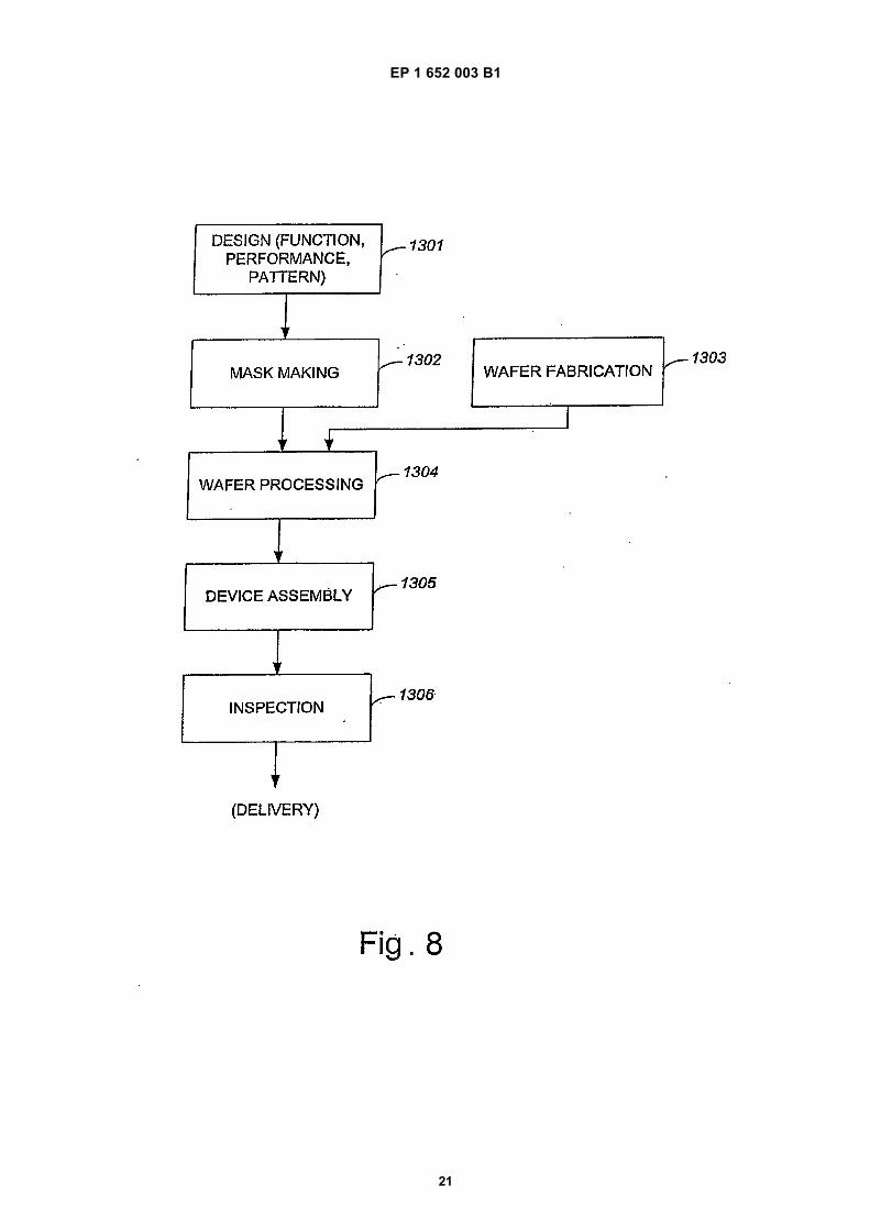
veloping mechanical interfaces, electrical circuit wiringconnections, and air pressure plumbing connections be-tween each subsystem. There is also a process whereeach subsystem is assembled prior to assembling a pho-tolithography system from the various subsystems. Oncea photolithography system is assembled using the vari-ous subsystems, an overall adjustment is generally per-formed to ensure that substantially every desired accu-racy is maintained within the overall photolithographysystem. Additionally, it may be desirable to manufacturean exposure system in a clean room where the temper-ature and humidity are controlled.[0054] Further, semiconductor devices may be fabri-cated using systems described above, as will be dis-cussed with reference to Fig. 8. The process begins atstep 1301 in which the function and performance char-acteristics of a semiconductor device are designed orotherwise determined. Next, in step 1302, a reticle(mask) in which has a pattern is designed based uponthe design of the semiconductor device. It should be ap-preciated that in a parallel step 1303, a wafer is madefrom a silicon material. The mask pattern designed instep 1302 is exposed onto the wafer fabricated in step1303 in step 1304 by a photolithography system. Oneprocess of exposing a mask pattern onto a wafer will bedescribed below with respect to Fig. 9. In step 1305, thesemiconductor device is assembled. The assembly ofthe semiconductor device generally includes, but is notlimited to, wafer dicing processes, bonding processes,and packaging processes. Finally, the completed deviceis inspected in step 1306.[0055] Fig. 9 is a process flow diagram which illustratesthe steps associated with wafer processing in the caseof fabricating semiconductor devices in accordance withan embodiment of the present invention. In step 1311,the surface of a wafer is oxidized. Then, in step 1312which is a chemical vapor deposition (CVD) step, an in-sulation film may be formed on the wafer surface. Oncethe insulation film is formed, in step 1313, electrodes areformed on the wafer by vapor deposition. Then, ions maybe implanted in the wafer using substantially any suitablemethod in step 1314. As will be appreciated by thoseskilled in the art, steps 1311-1314 are generally consid-ered to be preprocessing steps for wafers during waferprocessing. Further, it should be understood that selec-tions made in each step, e.g., the concentration of variouschemicals to use in forming an insulation film in step1312, may be made based upon processing require-ments.[0056] At each stage of wafer processing, when pre-processing steps have been completed, post-processingsteps may be implemented. During post-processing, in-itially, in step 1315, photoresist is applied to a wafer.Then, in step 1316, an exposure device may be used totransfer the circuit pattern of a reticle to a wafer. Trans-ferring the circuit pattern of the reticle of the wafer gen-erally includes scanning a reticle scanning stage whichmay, in one embodiment, include a force damper to
dampen vibrations.[0057] After the circuit pattern on a reticle is transferredto a wafer, the exposed wafer is developed in step 1317.Once the exposed wafer is developed, parts other thanresidual photoresist, e.g., the exposed material surface,may be removed by etching. Finally, in step 1319, anyunnecessary photoresist that remains after etching maybe removed. As will be appreciated by those skilled inthe art, multiple circuit patterns may be formed throughthe repetition of the preprocessing and post-processingsteps.[0058] Although only a few embodiments of the presentinvention have been described, it should be understoodthat the present invention may be embodied in many oth-er specific forms without departing from the spirit or thescope of the present invention. By way of example, al-though the use wafer table arrangement with a substan-tially flat overall planar surface of a uniform height hasbeen described as being suitable for use in an immersionlithography system to enable a small liquid-filled or fluid-filled gap to be maintained between a projection lens andthe surface of the wafer table, such a wafer table is notlimited to use as a part of an immersion lithography sys-tem.[0059] A table which supports an object to be scannedand has a relatively planar, substantially uniform top sur-face has generally been described as being a wafer table.Such a table is not limited to being a wafer table. Forinstance, a reticle table may also have a relatively planar,substantially uniform top surface. Alternatively, a sub-strate table supporting, for example, a glass plate for LCDmanufacturing, a microscope specimen, or the like mayalso have a substantially flat planar surface.[0060] Components which are supported within a wa-fer table arrangement such that top surfaces of the com-ponents are at substantially the same height as a topsurface of a wafer table have been described as includingdose sensors, dose uniformity sensors, aerial image sen-sors, reference flats, and fiducial marks. It should be ap-preciated, however, that any suitable additional compo-nents may be supported within the wafer table arrange-ment such that the top surfaces of the additional compo-nents are substantially flush with the top surface of thewafer table. Further, while a wafer table arrangementmay include a dose sensor or a dose uniformity sensor,an aerial image sensor, a reference flat, and a fiducialmark, a wafer table arrangement may not necessarilyinclude a dose sensor or a dose uniformity sensor, anaerial image sensor, a reference flat, and a fiducial mark.That is, a wafer table arrangement may include as littleas one component that has a top surface which is sub-stantially flush with the overall top surface of the wafertable arrangement.[0061] It should be appreciated that for substantiallyall components supported on a wafer table to have topsurfaces that are substantially flush with the overall topsurface of the a wafer table arrangement, the wafer tablearrangement may need to support a bottom surface of
15 16

EP 1 652 003 B1
10
5
10
15
20
25
30
35
40
45
50
55
each component at different heights. That is, the bottomsurfaces of the components may need to be supportedat different heights in order to enable the top surfaces ofthe components to be oriented such that the top surfacesare all substantially flush with the overall top surface ofthe wafer table arrangement.[0062] The materials used to form a wafer table ar-rangement, e.g., a wafer table and a plate which is posi-tioned atop the wafer table, may be widely varied. Al-though a plate has been described as being formed fromTeflon, it should be appreciated that the plate may beformed from substantially any suitable material. There-fore, the present examples are to be considered as illus-trative and not restrictive, and the invention is not to belimited to the details given herein, but may be modifiedwithin the scope of the appended claims.
Claims
1. An immersion lithography exposure apparatus com-prising:
a lens (684);a table assembly (602), the table assembly hav-ing a surface (614), the table assembly beingarranged to support at least a substrate, the sur-face of the table assembly having an opening toaccommodate the substrate, a surface of thesupported substrate being at substantially asame height as the surface of the table assem-bly; anda sensor (650) having a surface, the surface ofthe sensor being at substantially a same heightas the surface of the table assembly,wherein the apparatus is arranged to maintainlocally a liquid between the lens and the surfaceof the table assembly, between the lens and thesurface of the substrate, and/or between thelens and the surface of the sensor.
2. The immersion lithography exposure apparatus ofclaim 1, wherein the apparatus is arranged to permitthe sensor to be viewed through the lens with theliquid between the lens and the sensor.
3. The immersion lithography exposure apparatus ofclaim 1 or 2, further comprising:
a fiducial mark (650) having a surface, the sur-face of the fiducial mark being at substantially asame height as the surface of the table assem-bly, the apparatus being arranged to maintain aliquid between the lens and the surface of thetable assembly, between the lens and the sur-face of the substrate, between the lens and thesurface of the sensor, and/or between the lensand the surface of the fiducial mark.
4. The immersion lithography exposure apparatus ofany one of claims 1 to 3, wherein the table assemblyis a wafer table assembly and the substrate is a wa-fer.
5. The immersion lithography exposure apparatus ofclaim 4, wherein an overall top surface of the wafertable assembly which includes the surface of the wa-fer, the surface of the wafer table assembly, and thesurface of the sensor is substantially planar.
6. The immersion lithography exposure apparatus ofclaim 4 wherein the wafer table assembly defines aplurality of openings, and a first opening of the plu-rality of openings is arranged to substantially supportthe wafer and a second opening of the plurality ofopenings is arranged to substantially support thesensor.
7. The immersion lithography exposure apparatus ofany one of claims 1 to 6, wherein the sensor is atleast one of an aerial image sensor, a dose sensor,and a dose uniformity sensor.
8. The immersion lithography exposure apparatus ofany one of claims 1 to 7, wherein the table assemblyis arranged to support a substrate holder, the sub-strate holder being arranged to hold the substratesuch that the top substrate surface is at substantiallythe same height as the surface of the table assembly.
9. The immersion lithography exposure apparatus ofany one of claims 1 to 8, further including:
a retaining ring, the retaining ring being arrangedto enable a liquid to be substantially held be-tween a first surface of the lens and an overalltop surface of the table assembly, wherein theoverall top surface of the table assembly in-cludes the top surface of the substrate, the topsurface of the table assembly, and the top sur-face of the at least one sensor.
10. The immersion lithography exposure apparatus ofany one of claims 1 to 9, whereina part of the surface of the table assembly is arrangedbetween the surface of the sensor and the surfaceof the supported substrate.
11. The immersion lithography exposure apparatus ofany one of claims 1 to 10, whereineach of the surface of the table assembly, the surfaceof the sensor, and the surface of the supported sub-strate is capable of contacting with the liquid locallymaintained below the lens by moving the table as-sembly.
12. An immersion lithography exposure method com-
17 18

EP 1 652 003 B1
11
5
10
15
20
25
30
35
40
45
50
55
prising:
providing a lens (684), a table assembly (604)and a sensor (650), a surface of the sensor beingat substantially a same height as a surface ofthe table assembly;supporting a substrate by use of the table as-sembly, the surface of the table assembly havingan opening to accommodate the substrate, asurface of the supported substrate being at sub-stantially a same height as the surface of thetable assembly; andexposing the substrate via a liquid, the liquid be-ing maintained locally between the lens and thesurface of the table assembly, between the lensand the surface of the substrate, and/or betweenthe lens and the surface of the sensor.
13. The immersion lithography exposure method ofclaim 12, wherein the lens and sensor are so provid-ed as to permit the sensor to be viewed through thelens with the liquid between the lens and the sensor.
14. The immersion lithography exposure method ofclaim 12 or 13, wherein the method further comprisesthe step of providing a fiducial mark (650) having asurface, the surface of the fiducial mark being at sub-stantially a same height as the surface of the tableassembly; and a step of maintaining a liquid betweenthe lens and the surface of the table assembly, be-tween the lens and the surface of the substrate, be-tween the lens and the surface of the sensor, and/orbetween the lens and the surface of the fiducial mark.
15. The immersion lithography exposure method of anyone of claims 12 to 14, wherein the table assemblyis a wafer table assembly and the substrate is a wa-fer.
16. The immersion lithography exposure method ofclaim 15, wherein an overall top surface of the wafertable assembly which includes the surface of the wa-fer, the surface of the wafer table assembly, and thesurface of the sensor is substantially planar.
17. The immersion lithography exposure method ofclaim 16, wherein the wafer table assembly definesa plurality of openings, and a first opening of the plu-rality of openings substantially supports the waferand a second opening of the plurality of openingssubstantially supports the sensor.
18. The immersion lithography exposure method of anyone of claims 12 to 17, wherein the sensor is at leastone of an aerial image sensor, a dose sensor, anda dose uniformity sensor.
19. The immersion lithography exposure method of any
one of claims 12 to 18, wherein the table assemblysupports a substrate holder; and the substrate holderholds the substrate such that the top substrate sur-face is at substantially the same height as the surfaceof the table assembly.
20. The immersion lithography exposure method of anyone of claims 12 to 19, further including a step ofproviding a retaining ring, and in which method theretaining ring enables a liquid to be substantially heldbetween a first surface of the lens and an overall topsurface of the table assembly, wherein the overalltop surface of the table assembly includes the topsurface of the substrate, the top surface of the tableassembly, and the top surface of the at least onesensor.
21. The immersion lithography exposure method of anyone of claims 12 to 20, whereina part of the surface of the table assembly is arrangedbetween the surface of the sensor and the surfaceof the supported substrate.
22. The immersion lithography exposure method of anyone of claims 12 to 21, whereineach of the surface of the table assembly, the surfaceof the sensor, and the surface of the supported sub-strate is capable of contacting the liquid locally main-tained below the lens by moving the table assembly.
Patentansprüche
1. Immersionslithographiebelichtungsvorrichtung mit:
einer Linse (684);einem Tischaufbau (602), wobei der Tischauf-bau eine Fläche (614) aufweist, der Tischaufbauangeordnet ist, um mindestens ein Substrat zuunterstützen, die Fläche des Tischaufbaus eineÖffnung aufweist, um das Substrat aufzuneh-men, und eine Fläche des unterstützten Subst-rats im Wesentlichen auf einer gleichen Höhewie die Fläche des Tischaufbaus ist; undeinem Sensor (650), der eine Fläche aufweist,wobei die Fläche des Sensors im Wesentlicheneine gleiche Höhe wie die Fläche des Tischauf-baus aufweist,wobei die Vorrichtung angeordnet ist, um eineFlüssigkeit lokal zwischen der Linse und der Flä-che des Tischaufbaus, zwischen der Linse undder Fläche des Substrats und/oder zwischen derLinse und der Fläche des Sensors zu halten.
2. Immersionslithographiebelichtungsvorrichtungnach Anspruch 1, bei der die Vorrichtung angeordnetist, um zuzulassen, dass der Sensor mit der Flüssig-keit zwischen der Linse und dem Sensor durch die
19 20

EP 1 652 003 B1
12
5
10
15
20
25
30
35
40
45
50
55
Linse sichtbar ist.
3. Immersionslithographiebelichtungsvorrichtungnach Anspruch 1 oder 2, ferner mit:
einer Referenzmarkierung (650), die eine Flä-che aufweist, wobei die Fläche der Referenz-markierung im Wesentlichen eine gleiche Höhewie die Fläche des Tischaufbaus aufweist, dieVorrichtung angeordnet ist, um eine Flüssigkeitzwischen der Linse und der Fläche des Tisch-aufbaus, zwischen der Linse und der Fläche desSubstrats, zwischen der Linse und der Flächedes Sensors und/oder zwischen der Linse undder Fläche der Referenzmarkierung zu halten.
4. Immersionslithographiebelichtungsvorrichtungnach einem der Ansprüche 1 bis 3, bei welcher derTischaufbau ein Wafertischaufbau ist und das Sub-strat ein Wafer ist.
5. Immersionslithographiebelichtungsvorrichtungnach Anspruch 4, bei der eine obere Gesamtflächedes Wafertischaufbaus, der die Fläche des Wafersaufweist, die Fläche des Wafertischaufbaus und dieFläche des Sensors im Wesentlichen eben sind.
6. Immersionslithographiebelichtungsvorrichtungnach Anspruch 4, bei welcher der Wafertischaufbaueine Vielzahl von Öffnungen definiert und eine ersteÖffnung der Vielzahl von Öffnungen angeordnet ist,um den Wafer im Wesentlichen zu unterstützen, undeine zweite Öffnung der Vielzahl von Öffnungen an-geordnet ist, um im Wesentlichen den Sensor zu un-terstützen.
7. Immersionslithographiebelichtungsvorrichtungnach einem der Ansprüche 1 bis 6, bei welcher derSensor ein Luftbildsensor, ein Dosissensor und/oderein Dosiseinheitlichkeitssensor ist.
8. Immersionslithographiebelichtungsvorrichtungnach einem der Ansprüche 1 bis 7, bei welcher derTischaufbau angeordnet ist, um einen Substrathalterzu unterstützen, wobei der Substrathalter angeord-net ist, das Substrat so zu halten, dass die obereSubstratfläche im Wesentlichen auf der gleichen Hö-he ist wie die Fläche des Tischaufbaus.
9. Immersionslithographiebelichtungsvorrichtungnach einem der Ansprüche 1 bis 8, ferner mit:
einem Haltering, wobei der Haltering angeord-net ist, einer Flüssigkeit zu ermöglichen, im We-sentlichen zwischen einer ersten Fläche der Lin-se und einer oberen Gesamtfläche des Tisch-aufbaus gehalten zu werden, wobei die obereGesamtfläche des Tischaufbaus die obere Flä-
che des Substrats, die obere Fläche des Tisch-aufbaus und die obere Fläche des mindestenseinen Sensors aufweist.
10. Immersionslithographiebelichtungsvorrichtungnach einem der Ansprüche 1 bis 9, bei derein Teil der Fläche des Tischaufbaus zwischen derFläche des Sensors und der Fläche des unterstütz-ten Substrats angeordnet ist.
11. Immersionslithographiebelichtungsvorrichtungnach einem der Ansprüche 1 bis 10, bei derdie Fläche des Tischaufbaus, die Fläche des Sen-sors und die Fläche des unterstützten Substrats je-weils imstande sind, durch Bewegen des Tischauf-baus mit der Flüssigkeit in Kontakt zu kommen, dielokal unter der Linse gehalten wird.
12. Immersionslithographiebelichtungsverfahren mit:
Bereitstellen einer Linse (684), eines Tischauf-baus (604) und eines Sensors (650), wobei eineFläche des Sensors im Wesentlichen auf einergleichen Höhe ist wie eine Fläche des Tischauf-baus;Unterstützen eines Substrats durch Verwen-dung des Tischaufbaus, wobei die Fläche desTischaufbaus eine Öffnung aufweist, um dasSubstrat aufzunehmen, wobei eine Fläche desunterstützten Substrats im Wesentlichen auf ei-ner gleichen Höhe ist wie die Fläche des Tisch-aufbaus; undBelichten des Substrats über eine Flüssigkeit,wobei die Flüssigkeit lokal zwischen der Linseund der Fläche des Tischaufbaus, zwischen derLinse und der Fläche des Substrats und/oderzwischen der Linse und der Fläche des Sensorsgehalten wird.
13. Immersionslithographiebelichtungsverfahren nachAnspruch 12, bei dem die Linse und der Sensor sobereitgestellt sind, um zu ermöglichen, dass derSensor durch die Linse mit der Flüssigkeit zwischender Linse und dem Sensor zu sehen ist.
14. Immersionslithographiebelichtungsverfahren nachAnspruch 12 oder 13, wobei das Verfahren fernerden Schritt des Bereitstellens einer Referenzmarkie-rung (650) mit einer Fläche umfasst, wobei die Flä-che der Referenzmarkierung im Wesentlichen aufeiner gleichen Höhe wie die Fläche des Tischauf-baus ist; und einen Schritt des Haltens einer Flüs-sigkeit zwischen der Linse und der Fläche des Ti-schaufbaus, zwischen der Linse und der Fläche desSubstrats, zwischen der Linse und der Fläche desSensors und/oder zwischen der Linse und der Flä-che der Referenzmarkierung.
21 22

EP 1 652 003 B1
13
5
10
15
20
25
30
35
40
45
50
55
15. Immersionslithographiebelichtungsverfahren nacheinem der Ansprüche 12 bis 14, bei dem der Tisch-aufbau ein Wafertischaufbau ist und das Substratein Wafer ist.
16. Immersionslithographiebelichtungsverfahren nachAnspruch 15, bei dem eine obere Gesamtfläche desWafertischaufbaus, welche die Fläche des Wafers,die Fläche des Wafertischaufbaus und die Flächedes Sensors aufweist, im Wesentlichen eben ist.
17. Immersionslithographiebelichtungsverfahren nachAnspruch 16, bei dem der Wafertischaufbau eineVielzahl von Öffnungen definiert und eine erste Öff-nung der Vielzahl von Öffnungen im Wesentlichenden Wafer unterstützt und eine zweite Öffnung derVielzahl von Öffnungen im Wesentlichen den Sensorunterstützt.
18. Immersionslithographiebelichtungsverfahren nacheinem der Ansprüche 12 bis 17, bei dem der Sensorein Luftbildsensor, ein Dosissensor und/oder ein Do-siseinheitlichkeitssensor ist.
19. Immersionslithographiebelichtungsverfahren nacheinem der Ansprüche 12 bis 18, bei dem der Tisch-aufbau einen Substrathalter unterstützt und der Sub-strathalter das Substrat so hält, dass die obere Sub-stratfläche im Wesentlichen auf der gleichen Höheist wie die Fläche des Tischaufbaus.
20. Immersionslithographiebelichtungsverfahren nacheinem der Ansprüche 12 bis 19, ferner mit einemSchritt des Bereitstellens eines Halterings, wobei derHaltering in dem Verfahren einer Flüssigkeit ermög-licht, im Wesentlichen zwischen einer ersten Flächeder Linse und einer oberen Gesamtfläche des Tisch-aufbaus gehalten zu werden und die obere Gesamt-fläche des Tischaufbaus die obere Fläche des Sub-strats, die obere Fläche des Tischaufbaus und dieobere Fläche des mindestens einen Sensors auf-weist.
21. Immersionslithographiebelichtungsverfahren nacheinem der Ansprüche 12 bis 20, bei demein Teil der Fläche des Tischaufbaus zwischen derFläche des Sensors und der Fläche des unterstütz-ten Substrats angeordnet ist.
22. Immersionslithographiebelichtungsverfahren nacheinem der Ansprüche 12 bis 21, bei demdie Fläche des Tischaufbaus, die Fläche des Sen-sors und die Fläche des unterstützten Substrats je-weils imstande sind, durch Bewegen des Tischauf-baus mit der Flüssigkeit in Kontakt zu kommen, dielokal unter der Linse gehalten wird.
Revendications
1. Appareil d’exposition de lithographie par immersioncomprenant :
une lentille (684) ;un ensemble de plateau (602), l’ensemble deplateau ayant une surface (614), l’ensemble deplateau étant agencé pour supporter au moinsun substrat, la surface de l’ensemble de plateauayant une ouverture pour recevoir le substrat,une surface du substrat supporté étant substan-tiellement à une même hauteur que la surfacede l’ensemble de plateau ; etun capteur (650) ayant une surface, la surfacedu capteur étant substantiellement à une mêmehauteur que la surface de l’ensemble de plateau,dans lequel l’appareil est agencé pour maintenirlocalement un liquide entre la lentille et la sur-face de l’ensemble de plateau, entre la lentilleet la surface du substrat, et/ou entre la lentilleet la surface du capteur.
2. Appareil d’exposition de lithographie par immersionde la revendication 1, dans lequel l’appareil est agen-cé pour permettre au capteur d’être vu à travers lalentille avec le liquide entre la lentille et le capteur.
3. Appareil d’exposition de lithographie par immersionde la revendication 1 ou 2, comprenant en outre :
un repère de centrage (650) ayant une surface,la surface du repère de centrage étant substan-tiellement à une même hauteur que la surfacede l’ensemble de plateau, l’appareil étant agen-cé pour maintenir un liquide entre la lentille et lasurface de l’ensemble de plateau, entre la len-tille et la surface du substrat, entre la lentille etla surface du capteur, et/ou entre la lentille et lasurface du repère de centrage.
4. Appareil d’exposition de lithographie par immersionde l’une quelconque des revendications 1 à 3, danslequel l’ensemble de plateau est un ensemble deplateau de plaquette et le substrat est une plaquette.
5. Appareil d’exposition de lithographie par immersionde la revendication 4, dans lequel une surface su-périeure globale de l’ensemble de plateau de pla-quette qui comporte la surface de la plaquette, lasurface de l’ensemble de plateau de plaquette, et lasurface du capteur est substantiellement planaire.
6. Appareil d’exposition de lithographie par immersionde la revendication 4, dans lequel l’ensemble de pla-teau de plaquette définit une pluralité d’ouvertures,et une première ouverture de la pluralité d’ouverturesest agencée pour supporter substantiellement la pla-
23 24

EP 1 652 003 B1
14
5
10
15
20
25
30
35
40
45
50
55
quette et une deuxième ouverture de la pluralitéd’ouvertures est agencée pour supporter substan-tiellement le capteur.
7. Appareil d’exposition de lithographie par immersionde l’une quelconque des revendications 1 à 6, danslequel le capteur est au moins l’un d’un capteurd’image aérienne, d’un capteur de dose, et d’un cap-teur d’uniformité de dose.
8. Appareil d’exposition de lithographie par immersionde l’une quelconque des revendications 1 à 7, danslequel l’ensemble de plateau est agencé pour sup-porter un support de substrat, le support de substratétant agencé pour maintenir le substrat de sorte quela surface supérieure de substrat soit substantielle-ment à la même hauteur que la surface de l’ensem-ble de plateau.
9. Appareil d’exposition de lithographie par immersionde l’une quelconque des revendications 1 à 8, com-portant en outre :
une bague de retenue, la bague de retenue étantagencée pour permettre à un liquide d’être subs-tantiellement maintenu entre une première sur-face de la lentille et une surface supérieure glo-bale de l’ensemble de plateau, dans lequel lasurface supérieure globale de l’ensemble deplateau comporte la surface supérieure dusubstrat , la surface supérieure de l’ensemblede plateau, et la surface supérieure de l’aumoins un capteur.
10. Appareil d’exposition de lithographie par immersionde l’une quelconque des revendications 1 à 9, danslequelune partie de la surface de l’ensemble de plateauest agencée entre la surface du capteur et la surfacedu substrat supporté.
11. Appareil d’exposition de lithographie par immersionde l’une quelconque des revendications 1 à 10, danslequelchacune de la surface de l’ensemble de plateau, dela surface du capteur, et de la surface du substratsupporté est capable de venir en contact avec leliquide localement maintenu en dessous de la lentilleen déplaçant l’ensemble de plateau.
12. Procédé d’exposition de lithographie par immersioncomprenant le fait :
de fournir une lentille (684), un ensemble de pla-teau (604) et un capteur (650), une surface ducapteur étant substantiellement à une mêmehauteur qu’une surface de l’ensemble deplateau ;
de supporter un substrat par utilisation de l’en-semble de plateau, la surface de l’ensemble deplateau ayant une ouverture pour recevoir lesubstrat, une surface du substrat supporté étantsubstantiellement à une même hauteur que lasurface de l’ensemble de plateau ; etd’exposer le substrat via un liquide, le liquideétant maintenu localement entre la lentille et lasurface de l’ensemble de plateau, entre la len-tille et la surface du substrat, et/ou entre la len-tille et la surface du capteur.
13. Procédé d’exposition de lithographie par immersionde la revendication 12, dans lequel la lentille et lecapteur sont prévus de manière à permettre au cap-teur d’être vu à travers la lentille avec le liquide entrela lentille et le capteur.
14. Procédé d’exposition de lithographie par immersionde la revendication 12 ou 13, dans lequel le procédécomprend en outre l’étape qui consiste à fournir unrepère de centrage (650) ayant une surface, la sur-face du repère de centrage étant substantiellementà une même hauteur que la surface de l’ensemblede plateau ; et une étape qui consiste à maintenir unliquide entre la lentille et la surface de l’ensemble deplateau, entre la lentille et la surface du substrat,entre la lentille et la surface du capteur, et/ou entrela lentille et la surface du repère de centrage.
15. Procédé d’exposition de lithographie par immersionde l’une quelconque des revendications 12 à 14,dans lequel l’ensemble de plateau est un ensemblede plateau de plaquette et le substrat est une pla-quette.
16. Procédé d’exposition de lithographie par immersionde la revendication 15, dans lequel une surface su-périeure globale de l’ensemble de plateau de pla-quette qui comporte la surface de la plaquette, lasurface de l’ensemble de plateau de plaquette, et lasurface du capteur est substantiellement planaire.
17. Procédé d’exposition de lithographie par immersionde la revendication 16, dans lequel l’ensemble deplateau de plaquette définit une pluralité d’ouvertu-res, et une première ouverture de la pluralité d’ouver-tures supporte substantiellement la plaquette et unedeuxième ouverture de la pluralité d’ouvertures sup-porte substantiellement le capteur.
18. Procédé d’exposition de lithographie par immersionde l’une quelconque des revendications 12 à 17,dans lequel le capteur est au moins l’un d’un capteurd’image aérienne, d’un capteur de dose, et d’un cap-teur d’uniformité de dose.
19. Procédé d’exposition de lithographie par immersion
25 26

EP 1 652 003 B1
15
5
10
15
20
25
30
35
40
45
50
55
de l’une quelconque des revendications 12 à 18,dans lequel l’ensemble de plateau supporte un sup-port de substrat ; et le support de substrat maintientle substrat de sorte que la surface supérieure desubstrat soit substantiellement à la même hauteurque la surface de l’ensemble de plateau.
20. Procédé d’exposition de lithographie par immersionde l’une quelconque des revendications 12 à 19,comportant en outre une étape qui consiste à fournirune bague de retenue, et dans ce procédé la baguede retenue permet à un liquide d’être substantielle-ment maintenu entre une première surface de la len-tille et une surface supérieure globale de l’ensemblede plateau, dans lequel la surface supérieure globalede l’ensemble de plateau comporte la surface supé-rieure du substrat, la surface supérieure de l’ensem-ble de plateau, et la surface supérieure de l’au moinsun capteur.
21. Procédé d’exposition de lithographie par immersionde l’une quelconque des revendications 12 à 20,dans lequelune partie de la surface de l’ensemble de plateauest agencée entre la surface du capteur et la surfacedu substrat supporté.
22. Procédé d’exposition de lithographie par immersionde l’une quelconque des revendications 12 à 21,dans lequelchacune de la surface de l’ensemble de plateau, dela surface du capteur, et de la surface du substratsupporté est capable de venir en contact avec leliquide localement maintenu en dessous de la lentilleen déplaçant l’ensemble de plateau.
27 28

EP 1 652 003 B1
16

EP 1 652 003 B1
17

EP 1 652 003 B1
18
EP 1 652 003 B1
19

EP 1 652 003 B1
20
EP 1 652 003 B1
21

EP 1 652 003 B1
22

EP 1 652 003 B1
23

EP 1 652 003 B1
24

EP 1 652 003 B1
25
REFERENCES CITED IN THE DESCRIPTION
This list of references cited by the applicant is for the reader’s convenience only. It does not form part of the Europeanpatent document. Even though great care has been taken in compiling the references, errors or omissions cannot beexcluded and the EPO disclaims all liability in this regard.
Patent documents cited in the description
• US 5825043 A [0011]• EP 1429188 A2 [0012]• WO 2004090577 A2 [0012]• US 4465368 A [0024]• US 6078380 A [0024]• US 20020061469 A1 [0024]• US 20020041377 A1 [0024]• US 5985495 A [0024]• US 5243195 A [0024]• US 0410055 W [0030]• US 0409994 W [0030]• US 0410071 W [0030]• JP 8166475 A [0041] [0051]
• US 5528118 A [0041] [0049] [0051]• JP 8330224 A [0042] [0051]• US 5874820 A [0042] [0051]• JP 8171054 A [0048]• US 5668672 A [0048]• JP 10020195 A [0048]• US 5835275 A [0048]• JP 8334695 A [0048]• US 5689377 A [0048]• JP 10003039 A [0048]• US 5892117 A [0048]• US 5623853 A [0049]