(19) united states (12) patent application publication … · light absorbing films technological...
TRANSCRIPT
(19) United States (12) Patent Application Publication (10) Pub. No.: US 2017/0066932 A1
MAGDASS et al.
US 2017 OO66932A1
(43) Pub. Date: Mar. 9, 2017
(54) LIGHT ABSORBING FILMS
(71)
(72)
(73)
(21)
(22)
(86)
Applicants:
Inventors:
Assignees:
Appl. No.:
PCT Fed:
PCT No.:
S 371 (c)(1), (2) Date:
Yissum Research Development Company of the Hebrew University of Jerusalem Ltd, Jerusalem (IL); Nanyang Technological University, Singapore (SG)
Shlomo MAGDASSI, Jerusalem (IL); Camille ZWICKER, Jerusalem (IL); Subodh Gautam MHAISALKAR, Singapore (SG); Daniel MANDLER, Jerusalem (IL); Lihi LEVI, Rishon LeZion (IL); Suzanna AZOUBEL, Jerusalem (IL)
Yissum Research Development Company of the Hebrew University of Jerusalem Ltd, Jerusalem (IL); Nanyang Technological University, Singapore (SG)
15/122,846
Mar. 10, 2015
PCT/IL2015/05O251
Aug. 31, 2016
Related U.S. Application Data (60) Provisional application No. 61/950,279, filed on Mar.
10, 2014.
Publication Classification
(51) Int. Cl. C09D 5/32 (2006.01) CO3C 17/32 (2006.01) GO2B I/It (2006.01) C09D 7/12 (2006.01) GO2B 5/00 (2006.01)
(52) U.S. Cl. CPC ............... C09D 5/32 (2013.01); C09D 7/1216
(2013.01); G02B5/003 (2013.01); G02B I/10 (2013.01); C03C 17/32 (2013.01); YIOS
977/742 (2013.01); B82Y 20/00 (2013.01)
(57) ABSTRACT
Provided is a spectrally selective solar thermal coating, formed as a continuous uniform layer, combining a light absorbing coating and an infrared (IR) reflecting layer positioned on top of the absorber coating. The coating is adapted for use in a plurality of applications, including amongst many control of Stray light and absorptivity in thermosolar devices.

Patent Application Publication Mar. 9, 2017 Sheet 1 of 23 US 2017/0066932 A1
Patent Application Publication Mar. 9, 2017 Sheet 2 of 23 US 2017/0066932 A1
Waveleights in
Fig. 2(b)
Patent Application Publication Mar. 9, 2017 Sheet 3 of 23 US 2017/0066932 A1
OO
8
SS
94
92 S 1. 150 2. 25
wavelength (nm)
Patent Application Publication Mar. 9, 2017 Sheet 4 of 23 US 2017/0066932 A1
2 G S& S.
3. 3, 8S S. SS S.S 5. 8 : Wavelength (sir

Patent Application Publication Mar. 9, 2017 Sheet 5 of 23 US 2017/0066932 A1
1.
SS
SS
SS^x SXXXXXXXXXXX
SS
XXXXXXXXXXXXXXXXXXXXXXXXXXXXXXX
500 O 15 O s
wavelength (nm)
Fig. 5(a)
8
:
S
S :S

Patent Application Publication Mar. 9, 2017 Sheet 6 of 23 US 2017/0066932 A1
saweetists is:
Fig. 6

Patent Application Publication Mar. 9, 2017 Sheet 7 of 23 US 2017/0066932 A1
i. 40 SCO S. 8. 3S O
wavelength (nm)
Fig. 7

Patent Application Publication Mar. 9, 2017 Sheet 8 of 23 US 2017/0066932 A1
2,5 3 3,5 A. 4.5 S. SS 6 8,5 7
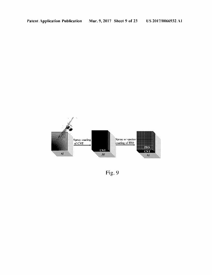
Patent Application Publication Mar. 9, 2017. Sheet 9 of 23 US 2017/0066932 A1

Patent Application Publication Mar. 9, 2017. Sheet 10 of 23 US 2017/0066932 A1
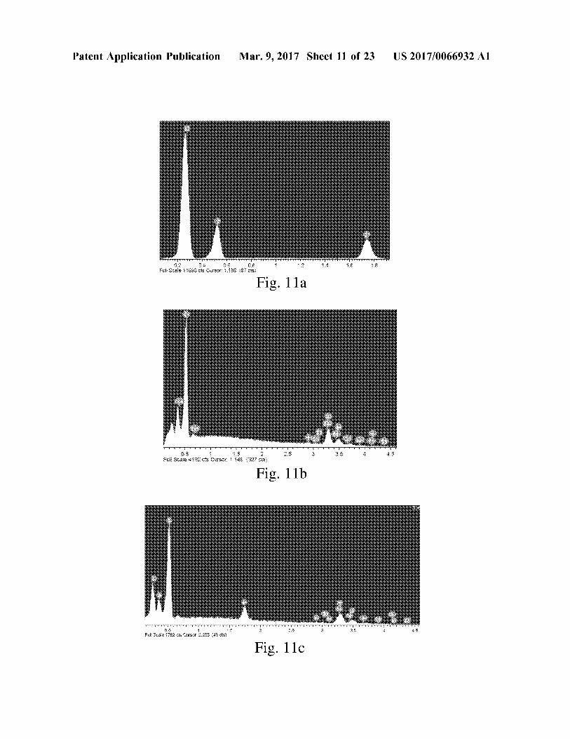
Patent Application Publication Mar. 9, 2017. Sheet 11 of 23 US 2017/0066932 A1
3.3 E. . F: Sass SSS is ser: SS 8 is
r-r-r-t-t-t-t-t-t-r-r-r------r-r 3. 3.S. &S
--r-r------ ls S : :S
83 Sigaea:E is Rsssf. R.E.
------ t-r-r---------------r-r--
Fig. 1 lb
as Scai is: cts Casor 3.255 (35:
Patent Application Publication Mar. 9, 2017. Sheet 12 of 23 US 2017/0066932 A1
Y-Y-Y-Y-Y-Y-Y-Y-Y-Y-Y- CN
Sprayed ITO - Sputtered ITO
10 20 30 40 50 60 70 20 (degree)
Fig. 12
Patent Application Publication Mar. 9, 2017. Sheet 13 of 23 US 2017/0066932 A1
O
5 O
400 800 1200 1600 2000 Wavelength (nm)
500 1000 1500 2000 Wavelength (nm)
Fig. 13
Patent Application Publication Mar. 9, 2017. Sheet 14 of 23 US 2017/0066932 A1
35
30 -CNT/ITOP" 25 w CNT/ITOP"
20
400 800 1200 1600 2000 Wavelength (nm)
Fig. 14
Patent Application Publication Mar. 9, 2017. Sheet 15 of 23 US 2017/0066932 A1
S s Š s s s
- S y s S XS sax
s s s s Absorptance s s sys &
O Š Emittance w w s S s
C S es sax S
Š Yas S NS s
ya Yasa s W: X
s s
s s S \, is
300 600 900 1200 Thickness (nm)
Fig. 15(a)
- CNT/ITO, M. CNT/ITO
CNT/ITO ------- CNT/ITO
CNT/ITO or CNT/ITO.
CNT/ITO N CNT/ITO or CNT/ITO
400 800 1200 1600 2000 Wavelength (nm)
Fig. 15(b)

Patent Application Publication Mar. 9, 2017. Sheet 16 of 23 US 2017/0066932 A1
11 36925 OOOOO g
O O 300 600 900 1200
Thickness (nm)
Fig. 16

Patent Application Publication Mar. 9, 2017. Sheet 17 of 23 US 2017/0066932 A1
Fig. 17(a)-(c)
S SS SS
Absorptance Absorptance
Emittance S Emittance SS, S S.S. O 6
& O. 4. S. S.
sess-starS' 50 100 150 200 250 300 O 12 24, 36 48 60 72 84 96
Temperature ("C) Time (hr)
S xx. s 0. 2 SS, s
Fig. 18a Fig. 18b


Patent Application Publication Mar. 9, 2017. Sheet 19 of 23 US 2017/0066932 A1
F: 33:83. 3s 83
v- S
swww.
S 3SS S.
ESSESs 8:8;
S
S. S&
Fig.20(b)
US 2017/0066932 A1 Mar. 9, 2017. Sheet 20 of 23 Patent Application Publication
s S. 8
T''{& 8tsiysis Siasier
^MS-Q)
^ MS E2c
Temperature (C)
Fig. 21
Patent Application Publication Mar. 9, 2017. Sheet 21 of 23 US 2017/0066932 A1
XX XX XX RS 8. xxxxxx x x SSS
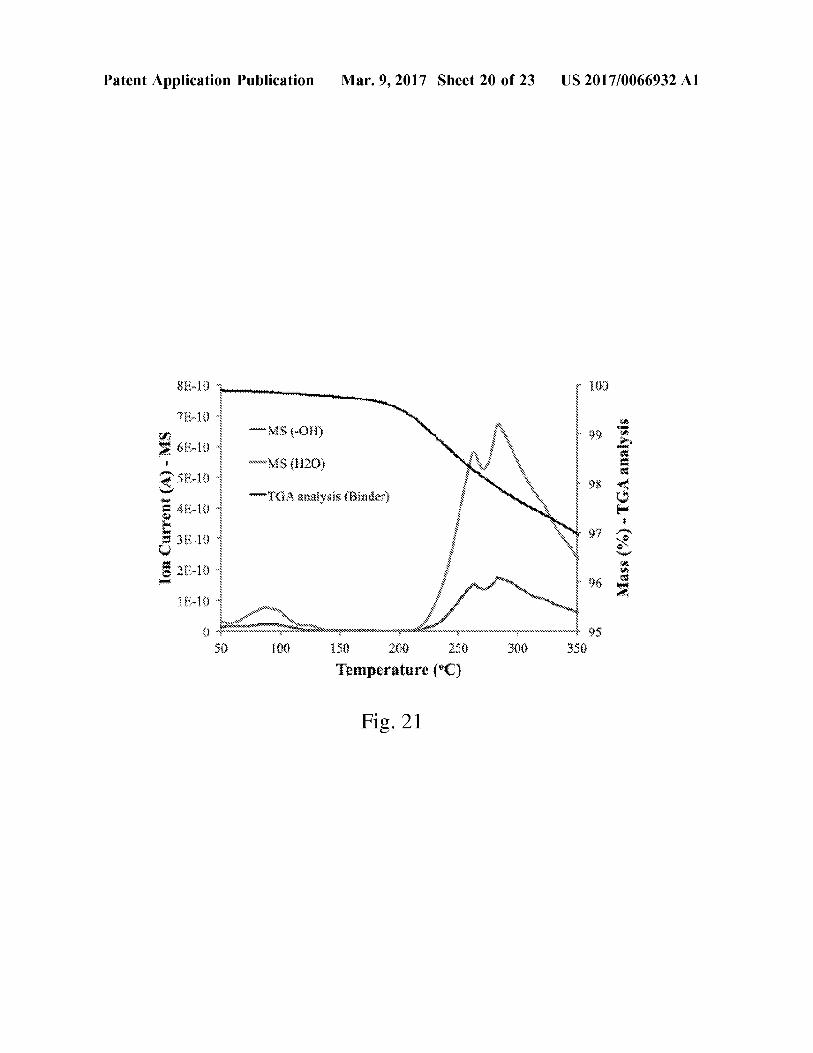
& Ysssssssssssss S&S
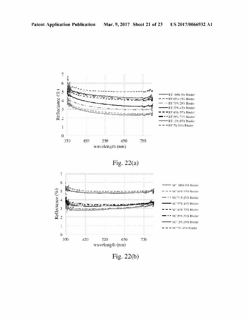
www
s & W. & NS:
X was was ;
& 3 * x sa
's as: s sa reser
S.K. as ... s:&SSassSS S. 3 ŠSSSSSSSSSS& re ;
a.
Fig. 22(b)

Patent Application Publication Mar. 9, 2017. Sheet 22 of 23 US 2017/0066932 A1
NC 85&S86, Binder NC 5798:436 Birder NC Sy:859, Birdier ASTM class 2B ASTM class; 3B ASM class; SB
Fig. 23

Patent Application Publication Mar. 9, 2017. Sheet 23 of 23 US 2017/0066932 A1
US 2017/0066932 A1
LIGHT ABSORBING FILMS
TECHNOLOGICAL FIELD
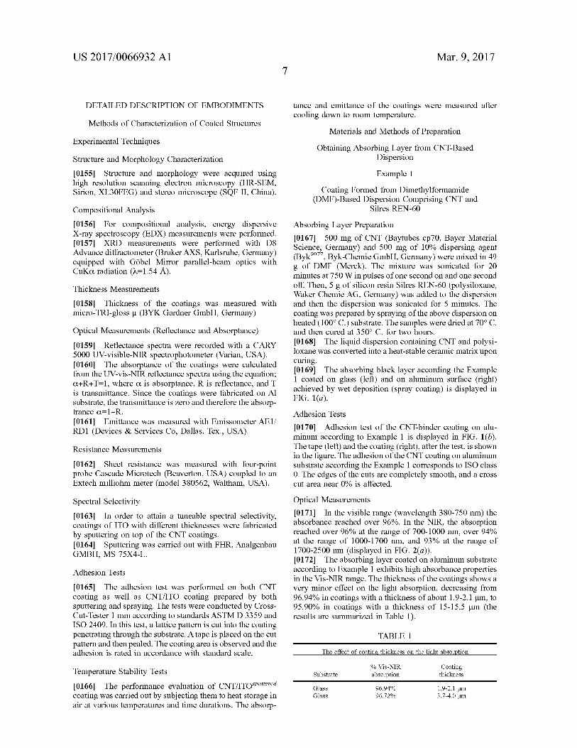
0001. The present disclosure generally relates to absorb ing formulations and uses thereof for coating structures.
BACKGROUND OF THE INVENTION
0002 The performance of optical devices, regardless of their complexity, is affected by stray light. The effect of stray light in optical systems may vary from low performance (reduced contrast on the image plane, obscure faint signals or false ones, false artifacts across the image plane, and magnitude errors in radiometric measurements) to physical damage (damaging fragile optical components and burning out detectors) 1. 0003 Stray light can be reduced to a tolerable level by proper design of the mechanical system or by using func tional black optical coatings in elements of the optical system. 0004. A functional optical absorbing coating can be made of an ideal black material which is capable of absorbing light, at all angles and over all wavelengths. Common methods for producing Such coatings are metal anodizing with an inorganic black coloring process 2-5 and electro less deposition of nickel oxide coating 6-9. Both methods require several process steps, including Substrate surface pre-treatment. 0005 Carbon nanotubes (CNTs) have unique electrical and mechanical properties, excellent light absorbing prop erties, and are therefore, ideal candidates for super black coating, especially when grown as vertically aligned forests. 0006 A CNT forest (aligned dense nanotubes placed perpendicularly to the Surface) has been used as optical coating 10. Although this type of coating shows good light absorption and some anti-reflective performance, its produc tion requires unique equipment and specific conditions, since the CNT forest, which is usually grown by chemical vapor deposition (CVD) under high temperature and pres Sure. This process has several drawbacks, such as the coating Substrate type and area, and poor adhesion to the Substrate. 0007 Strongly absorbing materials are also needed for forming functional, high-absorbing coatings for Solar energy conversion. Solar thermal energy/power is one of the leading approaches for Solar energy conversion, which is mainly used in concentrated solar power (CSP) systems. The com mon basis for all CSP technologies is the solar absorber 11 which collects the Solar spectrum and converts it into heat. This absorber may be subjected to extreme temperatures, depending on its final application. The key component in solar absorber is the spectrally solar selective absorbing coating. 0008 Candidates for such solar absorber layers, such as black Ni, black Cu, PbS, black chrome, spinels and metal oxides black paints 12, can be applied onto a variety of structural absorber plate materials, such as carbon Steel, galvanized steel, stainless Steel, copper and aluminum 12. However, most of the coating technologies involve vacuum (physical and chemical) deposition 13 and sputtering 14. 0009 Multi-walled carbon nanotubes (MWCNT) are exceptionally good absorbers, with a potential of reaching 99% absorption in the UV-visible range 15). CNT-contain ing films have a large Surface area and high thermal con ductivity 16, which enables rapid heat transfer from CNT
Mar. 9, 2017
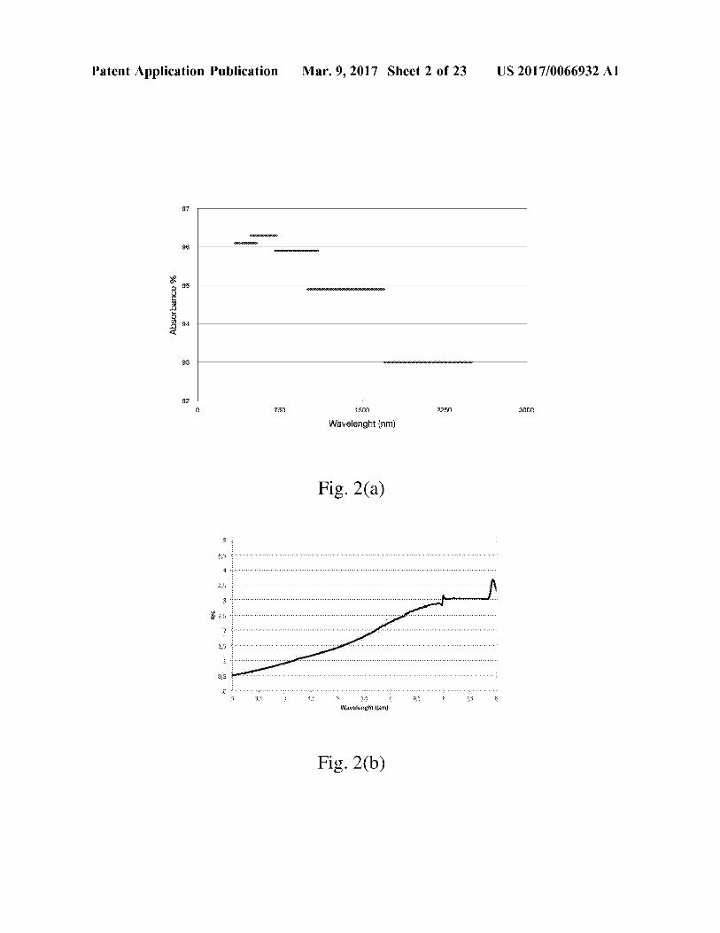
to the underlying metal. However, the studies 17-23 whereby CNT were used as solar absorber for solar thermal conversion did not achieve suitable results. (0010. In patent application US 2009/0314284 (35), solar coating was prepared by electrophoretic deposition of CNT together with alumina nanoparticles and PVP The highest absorptance of the resulting coatings was only 0.7, which is far below that required for thermal solar applications. In reality, an efficient solar selective absorber should have an absorptance of >0.9 and an emittance of <0.2. Most of these CNT based coatings showed poor spectral selectivity of absorption. Therefore, it is highly desired to develop spec trally Solar selective coating which has high absorptance, low emittance, good adhesion to the underlying metal Sub strate and high thermal stability for prolonged time. 0011 Beigbeder et al. 25 describe a cold control ther mal coating comprising polysiloxane (PDMS) resin filled with different conducting nanoparticles: indium tin oxide (ITO), Zinc oxide (ZnO) and multi-walled CNT with anti static properties and a high electrical conductivity. The CNT/PDMS composites exhibited electrical charges dissi pation under sirene irradiation but thermo-optical properties were too degraded. The thermal emissivity obtained was around 0.8.
REFERENCES
0012 (1 Frank Trager, Springer Handbook of Lasers and Optics, Springer, New York, 2007.
0013 2. Y. Goueffon, L. Arurault, C. Mabru, C. Tonon, P. Guigue, J. Mater. Process. Technol. 209 (2009) 5145 5151.
0014 3 A. K. Sharma, H. Bhojiraj, V. K. Kaila, H. Narayanamurthy, Met. Finish. 95 (1997) 14-20.
(0015 4 A. K. Sharma, R. U. Rani, H. Bhojaraj, H. Narayanamurthy, J. Appl. Electrochem. 23 (1993) 500 507.
(0016 (5 R. J. Fenolia, M. E. Marousek, D.C. Nagle, D. F. Shepard, High-temperature, high-emissivity, optically black boron surface, U.S. Pat. No. 5,035,949 (1991).
0017 6. V. Saxena, R. U. Rani, A. K. Sharma, Surf. Coat. Technol. 201 (2006) 855-862.
(0018 7 S. N. Kumar, L. K. Malhotra, K. L. Chopra, Sol. Energy Mater. 3 (1980) 519-532.
0019 8 R.J. C. Brown, P. J. Brewer, M. J. T. Milton, J. Mater. Chem. 12 (2002) 2749-2754.
0020 (9 R. U. Rani, A. K. Sharma, C. Minu, G. Poornima, S. Tejaswi, J. Appl. Electrochem. 40 (2010) 333-339.
0021 (10 K. Mizuno, J. Ishii, H. Kishida, Y. Hayamizu, S. Yasuda, D. N. Futaba, M. Yumura, K. Hata, PNAS 106 (2009) 6044-6047.
0022 11 IEA, Technology Roadmap Concentrating Solar Power, in, 2010.
0023 12 C. E. Kennedy, NREL/TP-520-31267, July 2002.
0024 13 N. Selvakumar, H. C. Barshilia, Sol. Energy Mater. Sol. Cells 2012, 98 1-23.
0025 14 Q.-C. Zhang, Sol. Energy Mater. Sol. Cells 2000, 62, 63-74.
0026 (15 J. G. Hagopian, S. A. Getty, M. Quijada, J. Tveekrem, R. Shiri, P. Roman, J. Butler, G. Georgiev. J. Livas, C. Hunt, A. Maldonado, Proc. of SPIE 2010, 7761, 7761 OF.

US 2017/0066932 A1
0027 (16 D. J. Yang, Q. Zhang, G. Chen, S. F. Yoon, J. Ahn, S. G. Wang, Q. Zhou, Q. Wang, and J. Q. Li, Phys. Rev. B 2002, 66, 165440.
0028. 17 A. Cao, X. Zhang, C. Xu, B. Wei, D. Wu, Sol. Energy Mater. Sol. Cells 2002, 70,481-486.
0029, 18 M. E. Rincon, J. D. Molina, M. Sanchez, C. Arancibia, E. Garcia, Sol. Energy Mater. Sol. Cells 2007, 91, 1421-1425.
0030) 19 K. Roro, N. Tile, B. Mwakikunga, B. Yalisi, A. Forbes, Mater. Sci. Eng. B 2012, 177, 581-587.
0031 (20 M. Kurzbock, G. M. Wallner, R. W. Lang, Energy Procedia 2012, 30, 438-445.
0032. 21 A. B. Kaul, J. B. Coles, M. Eastwood, R. O. Green, P. R. Bandaru, Small 2013, 9, 1058-1065.
0033 22 N. Selvakumar, S. B. Krupanidhi, H. C. Barshilia, Adv. Mater. 2014, 26, 2552-2557.
0034 (23 N. T. Panagiotopoulos, E. K. Diamanti, L. E. Koutsokeras, M. Baikousi, E. Kordatos, T. E. Matikas, D. Gournis, P. Patsalas, ACS Nano 2012, 6, 10475-10485.
0035 24 US 2009/0314284. 0036 (25 J. Beigbeder, P. Demont, S. Remaury, P. Nabarra and C. Lacabanne, “Incorporation of nanopar ticles in a flexible solar reflector for geostationary appli cations' (2009) in: http://esmatesa.int/materials news/ isme09/pdf/PROGRAMME ISMSE-2009.pdf.
SUMMARY OF THE INVENTION
0037. The objective of the present invention is to provide a non-reflective, high light-absorbing coating. This coating is performed by conventional air spraying process, is Suit able for rapid coverage of large areas of various Substrates. The resulting coatings are Suitable for stray light absorption in optical devices, can be easily performed for complex 3D structures, and due to their excellent adhesion are suitable for use in space or terrestrial applications. 0038. The invention disclosed herein provides a light absorbing black coating with light absorbance of at least 90%. To ensure a good adhesion of the black coating to a substrate, the absorbing material was combined with a heat resistant binder, at various weight ratios, to provide, after heating, a ceramic coating about 2-20 um thick. 0039. The invention further provides a spectrally selec tive Solar thermal coating, formed as a continuous and uniform layer which combines the light-absorbing coating and an infrared (IR) reflecting layer positioned on top of the absorber coating. The coating of the invention exhibits excellent spectral selectivity with high absorptance of 0.927 and low emittance of 0.2. The deposition of the reflecting layer, e.g. ITO on an absorber coating, e.g., made of CNT, decreased the emissivity by at least 20% as compared to a coating without a reflecting layer. 0040. The coatings of the invention may be used in a plurality of applications, including amongst many as means to control stray light and as means to improve absorptivity in thermosolar devices. 0041 As known in the art, “stray light' is unwanted light in an optical system, which may be a minor annoyance, in Some applications, but in others, such as in space-based technologies, such as a space-based telescope, it may result in the loss of important data. The negative effect stray light may have on a variety of optical systems makes it necessary to design optical systems which are capable of minimizing or at least capable of controlling it.
Mar. 9, 2017
0042. Thus, the invention generally provides means to control Stray light, e.g., in an optical device, the means being in a form of a Substrate coated with at least one light absorbing material, having a light absorbance of at least 90% (absorptivity above 0.90). 0043. In a first aspect, there is provided an element coated on at least a region of its surface with (a film or layer or coat of) at least one light-absorbing material, the light-absorbing material being associated with said at least a region via a binder material, such that the light absorbance of the film, layer or coat is at least 90%. The element of the invention is Suited for Stray-light Suppression. 0044 As used herein, the term “light suppression” refers to the ability of an element of the invention to absorb stray light, in some embodiments, at least 90% (or 91%, 92%, 93%, 94%, 95%, 96%, 97%, 98% or 99% of the light) of stray light directed at or in the vicinity of the element. As the element of the invention has an extremely high light absorbing characteristic, it may be regarded as Suppressing light or as black. 0045. The element may additionally be used to serve to remove heat from instruments and devices in which it is utilized and radiate it away. This ability of an element of the invention cools the instrument or device to lower tempera tures, in combination with its high light-absorbing capabili ties, render the instrument or device more sensitive to, e.g., faint signals. 0046. In some embodiments, the element of the invention comprises a substrate coated on at least a region thereof with a coat or film comprising at least one binder material which comprises or contains or embeds the at least one light absorbing material, and optionally at least one additive, the light-absorbance of the coat or film being at least 90%. 0047. In some embodiments, the light absorbance is of 90%, 91%, 92%, 93%, 94%, 95%, 96%, 97%, 98% or 99%. In other embodiments, light absorbance is of between 90% and 99%, between 90% and 98%, between 90% and 97%, between 90% and 96%, between 90% and 95%, between 90% and 94%, between 90% and 93%, between 90% and 92% or between 90% and 91%. 0048. The amount of the binder material and the at least one light-absorbing material is adapted to permit, at one hand, maximal light absorption, and at the other hand, effective binding of the light-absorbing material to a surface region of the substrate. In some embodiments, the film comprises at least 1% of the light-absorbing material. In other embodiments, the film comprises at most 10% of the light-absorbing material. In further embodiments, the film comprises between 1% and 10% of the light-absorbing material. 0049. In further embodiments, the film comprises 1, 2, 3, 4, 5, 6, 7, 8, 9, or 10% (w/w) of the light absorbing material. 0050. In some embodiments, the film comprises between 1 and 5%, between 2 and 6%, between 3 and 7%, between 4 and 8%, between 5 and 9% or between 6 and 10% of the light absorbing material. 0051. Thus, in some embodiments, the invention pro vides an element comprising a Substrate coated on at least a region thereof with a coat or film of at least one binder material which comprises or contains or embeds at least one light-absorbing material in an amount between 1 and 10% (w/w), relative to the amount of the binder, and optionally at least one additive, the light-absorbance of the coat or film being at least 90%.

US 2017/0066932 A1
0.052. In a film of the invention, the binder material adds up the composition to 100%. Thus, in some embodiments, the film comprises between 99% and 90% binder material. For example, where the film comprises 1% of the light absorbing material, the binder material constitutes 99% of the film. Similarly, where the film comprises 7% of the light absorbing material, the binder material constitutes 93%. 0053. In some embodiments, the invention provides a Substrate coated with a film of at least one binder, e.g., a ceramic material, and at least one light-absorbing material, e.g., carbon nanotube (CNT), wherein the at least one light-absorbing material constitutes at least 1% (w/w) of the film. In some embodiments, the film has an absorbance of 90%, 91%, 92%, 93%, 94%, 95%, 96%, 97%, 98% or 99%. In other embodiments, light absorbance is of between 90% and 99%, between 90% and 98%, between 90% and 97%, between 90% and 96%, between 90% and 95%, between 90% and 94%, between 90% and 93%, between 90% and 92% or between 90% and 91%. 0054 The at least one “light-absorbing material' is a material capable of absorbing Solar radiation, thus forming a “black coat on a surface region of the substrate. In some embodiments, the material absorbs light in the ultraviolet and visible spectrum as well as in the longer or far-infrared bands. The light absorbing material is selected to afford at least 90% absorbance (absorptivity above 0.90). In some embodiments, the light absorbing material is selected to provide an absorbance of 90%, 91%, 92%, 93%, 94%, 95%, 96%, 97%, 98% or 99%. In other embodiments, the light absorbing material is selected to provide absorbance of between 90% and 99%, between 90% and 98%, between 90% and 97%, between 90% and 96%, between 90% and 95%, between 90% and 94%, between 90% and 93%, between 90% and 92% or between 90% and 91%. 0055. In some embodiments, in the visible range (380 750 nm), light absorbance is at least 96%. In some embodi ments, in the NIR range (700-1,000 nm), light absorption is at least 96%. In some embodiments, at a wavelength of between 1,000-1,700 nm, light absorbance is at least 94%, and is at least 93% at a wavelength range of 1,700-2,500 nm. 0056. In some embodiments, the light absorbing material
is a carbon allotrope. In further embodiments, the light absorbing material is selected from carbon nanotubes (CNTs), graphene and fullerenes. In some embodiments, the light-absorbing material is CNT. 0057. As used herein, the term “carbon nanotubes (CNTs) refers to multi-walled CNTs as well as to single walled CNTs and double-walled CNTs and to mixtures thereof. The CNTs utilized in accordance with the present invention may vary in length, ranging from between about 1 micron to about 500 microns. The CNTs may also be selected amongst Such being less than about 1 micron in length, or greater than 500 microns. 0.058. In some embodiments, the CNTs are selected to have a length from about 1 micron to about 10 microns, from about 5 to 70 microns, from about 10 to about 100 microns or from about 100 to about 500 microns.
0059. In some embodiments, the CNTs utilized in ele ments of the invention vary in size (length and/or diameter) and composition. 0060. In some embodiments, an element of the invention comprises a Substrate coated on at least a region thereof with a coat or film of at least one binder material which comprises or contains or embeds CNT in an amount between 1 and
Mar. 9, 2017
10% (w/w), relative to the amount of the binder, and optionally at least one additive, the light-absorbance of the coat or film being at least 90%. 0061. To address the need for utilizing CNTs as light absorbing materials in elements of the invention, the ques tion of nanotube growth from gas phase on the element Surfaces was considered. In the course of research it was determined that best results were obtained when CNTs were utilized in an amount of between 1% and 10% w/w in the coating, embedded in a solid binder material, which at one hand could maximize adhesion of the CNTs to the surface and at the same time did not substantially affect Stray light Suppression or light absorption. 0062 CNT grown on the surface without a solid binder exhibited poor adhesion, irrespective of the orientation of the CNTs on the surface. When CNTs were utilized as part of a sticking layer, e.g., in the form of a thin film of a binder material, in which the CNTs were embedded, as a random distribution of CNTs, which may or may not be co-aligned with the surface, the method was found straightforward and free of deteriorating effects impacting CNT constitution, adhesion and stray light Suppression. In a coat or film of the binder material and CNTs are presented as a blend of the two materials, the CNTs not being typically oriented vertically (perpendicularly) to the Surface. 0063. The “binder material' is typically a material capable of associating, binding or permitting association between the surface of the substrate and the at least one light absorbing material. The binder material is typically selected amongst inorganic materials configured to receive a disper sion of the at least one light-absorbing material. In some embodiments, the binder material is a heat resistant ceramic material.
0064. In accordance with the present invention, the binder material is selected amongst ceramic materials char acterized by high thermal stability (service temperatures above, e.g., 300° C.), low shrinkage, high stability of shape and high dimensional accuracy. The ceramic materials are typically selected amongst inorganic-organic polymers or monomers, such as polysiloxanes, polyborosiloxane, poly silaZane, methyl trimethoxysilane and alumina precursors. The formation of ceramic material is based on thermal curing of the functionalized resins at temperatures above 300° C.
0065. The binder material may contain at least one addi tive. Such as dispersing, rheological and wetting agents. 0066. In some embodiments, the binder is thermally formed into a ceramic matrix which comprises the at least one light-absorbing material. Thus, a composite useful in the manufacture of films of the invention comprises at least one binder material in a non-polymerized form, at least one light-absorbing material and optionally at least one addi tional additive, the composite being transformable into the ceramic matrix by thermal treatment at a temperature above 300° C. The non-polymerized binder material is selected amongst silicon-based material Such as polyborosiloxane, polysilaZane, methyl trimethoxysilane polycarbosilane, sila Zane and polysiloxanes. 0067. In some embodiments, the silicon-based material is selected from polyorganosiloxane-based compound, a poly carbosilane-based compound, a polysilane-based com pound, a polysilaZane-based compound, and the like.

US 2017/0066932 A1
0068. In some embodiments, the silicon-based material is a polysiloxane-based compound. In some embodiments, the material is PDMS.
0069. In some embodiments, the silicon-based material is selected from precursor components comprising one or more reactive silicone containing polymers (and/or oligomers or formulations comprising same). Non-limiting examples of silicone containing polymers include linear or branched polysiloxanes with multiple reactive groups such as Si-H (silicon hydride), hydroxy, alkoxy, amine, chlorine, epoxide, isocyanate, isothiocyanate, nitrile, vinyl, or thiol functional groups.
0070. In some embodiments, the silicon-based material is selected from trimethoxymethylsilane, methyltrimethoxysi lane and polysiloxane. 0071. In some embodiments, the silicon-based material is selected from polysilane-based compounds, including homopolymers such as a polydialkylsilane (Such as poly dimethylsilane, poly(methylpropylsilane), poly(methylbu tylsilane), poly(methylpentylsilane), poly(dibutylsilane), and poly(dihexylsilane)), a polydiarylsilane (such as poly (diphenylsilane)), a poly(alkylarylsilane) (such as poly(m- ethylphenylsilane)); copolymers such as a copolymer of a dialkylsilane and another dialkylsilane (such as dimethylsi lane-methylhexylsilane copolymer), an arylsilane-alkylaryl silane copolymer (Such as phenylsilane-methylphenylsilane copolymer), and a dialkylsilane-alkylarylsilane copolymer (such as dimethylsilane-methylphenylsilane copolymer, dimethylsilane-phenylhexylsilane copolymer, dimethylsi lane-methylnaphthylsilane copolymer, and methylpropylsi lane-methylphenylsilane copolymer); and the like. 0072. In some embodiments, the polymerized ceramic coating or film comprising the at least one light-absorbing material, e.g., CNT, is at least 1 um thick. In some embodi ments, the coating is at most 20 um thick. In some embodi ments, the coating is between 1 and 20 um thick. In some embodiments, the coating is 1, 2, 3, 4, 5, 6, 7, 8, 9, 10, 11, 12, 13, 14, 15, 16, 17, 18, 19 or 20 um thick. 0073. In some embodiments, the coating is between 1 and 2 um thick. In some embodiments, the coating is between 1 and 5, between 1 and 4, between 1 and 3 um thick. 0074. In some embodiments, the coating is between 1.5 and 2.1 um thick. In some embodiments, the coating is between 1.9 and 2.1 um thick. In some embodiments, the coating is between 3.7 and 4 um thick. 0075. In some embodiments, the coating on the substrate
is of a ceramic material embedding, e.g., CNT, the material ratio between the ceramic material and the CNT being between 1:1 and 3:1.
0076. In some embodiments, the invention provides a Substrate coated with a film of at least one binder, e.g., a ceramic material, and at least one light-absorbing material, e.g., carbon nanotube (CNT), the coat being between 2 and 5um thick, wherein the at least one light-absorbing material constitutes at least 1% (w/w) of the film and wherein the coat having an absorbance of at least 90%. 0077. From the examples provided herein, it is clear that CNT absorbs solar light strongly and reflects weakly, thereby providing a Superior candidate as Solar light absorber. However, in Solar energy conversion applications, a coating of CNT may suffer from radiative emissivity in the IR region, which results in overheating of the layer of material serving as an absorbing Surface, and thus, in an
Mar. 9, 2017
increase of heat loss by convection, heat transfer and re emission of additional heat by the surface. 0078 Thus, for solar energy conversion applications, in order to inhibit the radiative emission of CNT coatings in the IR region and make the coating selective for Solar-thermal conversion, two approaches have been utilized: (1) modify ing the type of the binder, the ratio between the binder and CNT, thus forming a concentration gradient of the CNT throughout the deposited layer, and (2) adding an additional coating layer on top of the CNT absorbing layer. The layers may be different coating formulations for each layer, or by combining several functional additives within one or more coating layers. (0079. Without being bound by theory, the emissivity of the CNT coating depends on the type of the binder used in the formulation process. Al-O, trimethoxymethyl silane, and Ren 100 (resulting in silica and silicon containing polymers) were tested as binders and Baytube and Nanoyl tube were tested as absorbing materials. 0080. In some embodiments, inhibition of the radiative emission of the CNT in the IR region was achieved by coating the CNT layer with a material transparent to solar region but which reflects light in the IR region. 0081. Thus, in such embodiments, the binder/CNT coat ing is further provided with an infrared (IR) reflecting layer; thus providing on the Substrate a bilayer comprising:
0082 a first layer of a composite comprising at least one binder material, e.g., a ceramic material and at least one light-absorbing material; and
0.083 a second layer comprising an infrared (IR) reflecting material; the second layer being most exposed top layer.
I0084. The bilayer exhibits the inverse tandem ability to absorb substantially all stray light, as defined herein, and the ability to internalize evolved IR (thermal) radiation, thereby reducing the radiative emission in the IR region. Thus, a film of the invention may be regarded as an inverse tandem absorbing material, being transparent in the Solar region but reflecting light in the IR region. I0085 Thus, the “infrared (IR) reflecting material” is a material transparent to solar radiation but capable of reflect ing IR radiation. The material is selected from SnO2. In O, In doped SnO, (ITO), Sb doped SnO, (ATO), CdSnO, SiC. GaN, AlN, BN, HfC and LaB. I0086. In some embodiments, the IR reflecting material is or comprises ITO. I0087. The layer of the IR reflecting material is typically of a thickness between 400 and 3,000 nm, 500 and 3,000 nm, 600 and 3,000 nm, 700 and 3,000 nm, 800 and 3,000 nm, 900 and 3,000 nm, 1,000 and 3,000 nm, 1,100 and 3,000 nm, 1,200 and 3,000 nm, 1,300 and 3,000 nm, 1,400 and 3,000 nm, 1,500 and 3,000 nm, 1,600 and 3,000 nm, 1,700 and 3,000 nm, 1,800 and 3,000 nm, 1,900 and 3,000 nm, 2,000 and 3,000 nm or 2,500 and 3,000 nm. 0088. In some embodiments, the thickness of the IR reflecting layer is at least 400 nm, 500, 600, 700, 800, 900, 1,000, 1,100, 1,200, 1,300, 1,400, 1,500, 1,600, 1,700, 1,800, 1900, 2,000 or 2,500 nm. I0089. In some embodiments, the bilayer comprising a first layer of a composite comprising at least one binder material, e.g., a ceramic material and at least one light absorbing material, e.g., CNTs; and a second layer compris ing an infrared (IR) reflecting material has emissivity below 0.8 at the NIR range. In some embodiments, the emissivity
US 2017/0066932 A1
is below 0.7, below 0.6, below 0.5, below 0.4, below 0.3, below 0.2, below 0.1, below 0.05, below 0.01 or below 0.005 at the NIR range. 0090. In some embodiments, the emissivity is between 0.1 and 0.5. In some embodiments, the emissivity is between 0.1 and 0.4. In some embodiments, the emissivity is between 0.1 and 0.3. 0091. In some embodiments, the coated surface may further comprise an anti-reflective layer comprising an anti reflective material selected from silane, siloxane, silica, alumina, silicon carbide, hafnium carbide, gallium nitrate, aluminum nitrate, boron nitrate, SnO, CdSnO, InO and LaB. 0092. Thus, the invention further provides a bilayer, as defined herein, on a surface region of a Substrate, wherein each of the layers may be independently and optionally defined as herein. 0093. The bilayer may be further provided with at least one further coating or layer. 0094. The substrate onto which the ceramic coating or the bilayer is formed is selected of a material Such as a metal, glass, an inorganic semiconductor material, a polymeric material and a ceramic material. The Substrate may be a two-dimensional Substrate or a three-dimensional Substrate. The coating with the ceramic coating or with the bilayer may be on any region of the Substrate Surface, which may be planar or three-dimensional. 0.095. In some embodiments, the substrate or a surface of the substrate is of a material selected from a metal, glass, an inorganic or organic semiconductor material, a polymeric material and a ceramic material. In some embodiments, the Substrate or a Surface of the Substrate is made of or contains at least one metal. In some embodiments, the metal is selected from aluminum, stainless steel, gold, silver and copper. 0096. In some embodiments, the substrate or a surface of the Substrate is aluminum. 0097. The coating formed on a surface of the substrate may be a continuous pattern of a predetermined size and shape, which may or may not cover the full surface of the substrate. In some embodiments, the substrate is fully cov ered with a coat of the invention. In other embodiments, multiple patterns are formed on the Surface, in spaced-apart regions thereof. 0098. The coated surface is characterized by at least one or more of the following: 0099 (a) emissivity below 0.8 in the NIR range; 0100 (b) absorptivity above 0.90; 0101 (c) adhesion above 90% or having adhesion clas sification according to ASTM D3359 in the range of OB-3B or according to ISO 2409 Class 5-2: 0102 (d) reflectivity below 7% in the NIR range (850 2,400 nm); and/or (0103 (e) thermal stability at a temperature above 300° C. 0104. In some embodiments, the coated surface is char acterized by emissivity below 0.8, 0.6,0.5,0.4, 0.3 or 0.25 in the NIR range. In some embodiments, the coated surface has reflectivity below 7% in the NIR range. 0105. In some embodiments, the element of the invention for use in the Suppression of stray light comprises a ceramic material embedding a plurality of CNTs, the element being characterized by emissivity below 0.8 in the NIR range; absorptivity above 0.90; adhesion above 90%; and reflec tivity below 7% in the NIR range.
Mar. 9, 2017
0106. In some embodiments, the element of the invention for use in the Suppression of stray light comprises a ceramic material embedding a plurality of CNTs, the element being characterized by emissivity below 0.8 in the NIR range and absorptivity above 0.90. 0107. In some embodiments, the element of the invention for use in the reflection of IR radiation comprises a ceramic material embedding a plurality of CNTs and a coat of at least one IR reflecting material, such as ITO, the element being characterized by emissivity below 0.8 in the NIR range; adhesion above 90%; and reflectivity below 7% in the NIR range. 0108. In some embodiments, the element of the invention for use in the reflection of IR radiation comprises a ceramic material embedding a plurality of CNTs and a coat of ITO, the element being characterized by emissivity between 0.1 and 0.5 in the NIR range and absorptivity above 0.90. 0.109 The substrate coated in accordance with the inven tion may be a Substrate of a surface of a device or an instrument selected in general terms from optical, electronic and optoelectronic devices. Each of the elements of the invention may be utilized as components utilized in the construction of an optical, electronic or optoelectronic device. The device may be selected from an electronic device, optical device, an optoelectronic device, a photo thermal device, an energy conversion device, a Solar cell device and a satellite. In some embodiments, the device is selected from a photothermal device, an energy conversion device such as thermosolar device, and an optical device. The thermosolar device can be used for generating electric ity through generators, or for heating liquids such as water. 0110. In some embodiments, the thermosolar device is selected from Solar panels (e.g., water panels and building panels) and photovoltaic devices. 0111. In some embodiments, the device is or comprises a solar radiation absorber. 0112 Thus, the invention further provides a device com prising a substrate coated with at least one light-absorbing layer, the absorbing layer comprising a ceramic material and at least one light-absorbing material, wherein said at least one light-absorbing layer is optionally coated with a film of at least one Solar radiation transparent and IR radiation reflecting layer. 0113. The invention provides a thermosolar device com prising an element according to the invention. In some embodiments, the device is or comprises a solar panel. In Some embodiments, the Solar panel is selected amongst thermosolar water panels and thermosolar building panels. In some embodiments, the device is utilized for generating electricity or for heating a liquid. 0114. Similarly, elements of the invention may be used in satellite optics, satellite star-tracking, space telescopes, mis sile seeker devices, IR optical systems, cameras, micro Scopes, digital cinema cameras and thermal Solar collectors. 0115 The invention further provides a method of fabri cating an absorbent coating on a Surface region of a Sub strate, the method comprising:
0116 (a) forming on a Surface region at least one absorbing layer comprising: 0117 (i) a light-absorbing material; 0118 (ii) a polymerizable binder resin:
0119 (b) heating said at least one absorbing layer to induce polymerization and conversion into a heat resis tant material of said binder resin; and
US 2017/0066932 A1
I0120 (c) optionally forming at least one IR radiation reflecting layer on said polymerized binder.
0121. In some embodiments, the at least one IR radiation reflecting layer comprises a material selected from SnO, In O. In doped SnO (ITO), Sb doped SnO (ATO), CdSnO, SiC. GaN, AlN, BN, Hf, and LaB. 0122. In some embodiments, the method further com prises annealing said at least one IR radiation reflecting layer. 0123. In some embodiments, the forming of layer (a) is carried out by wet deposition. In some embodiments, the wet deposition is selected from spin coating, roll coating, coil coating, dip coating and spray deposition. In some embodi ments, the wet deposition is spray deposition of a dispersion comprising at least one light-absorbing material and at least one polymerizable binder. 0.124. In some embodiments, layer (c) is formed by wet deposition or by Sputtering deposition. In some embodi ments, the wet deposition is spray deposition of a mixture comprising at least one ceramic polymer precursor and optionally a binder in a solvent. 0.125. The invention further provides an ink formulation comprising at least one light-absorbing material, at least one polymerizable binder resin and at least one additive selected from a dispersant, a surfactant, a wetting agent, and a rheological agent. The formulation may further comprise at least one solvent (selected amongst organic solvents and aqueous media). 0126. In some embodiments, the formulation is adapted or suited for use in a method for fabricating a device for light Suppression. In further embodiments, the formulation is adapted or Suited for use in a method for fabricating a thermosolar device.
0127. In some embodiments, the formulation is used in a method for fabricating a ceramic film on a Surface region. In some embodiments, the at least one polymerizable binder resin is selected to thermally transform into a ceramic material, the transformation being optionally achievable by thermal treatment at a temperature above 300° C. The at least one polymerizable binder resin is selected amongst silicon-based materials such as polyborosiloxane, polysila Zane, methyl trimethoxysilane polycarbosilane, silaZane and polysiloxanes. 0128. In some embodiments, the at least one light-ab Sorbing material is selected as above, being preferably, in further embodiments, CNT.
BRIEF DESCRIPTION OF THE DRAWINGS
0129. In order to better understand the subject matter that is disclosed herein and to exemplify how it may be carried out in practice, embodiments will now be described, by way of non-limiting example only, with reference to the accom panying drawings, in which: 0130 FIG. 1(a). Black coating on glass (left) and alumi num Surface (right) achieved by wet deposition (spray coating) of the MWCNT formulation, and (b) adhesion test of CNT-binder formulation coated on aluminum substrate according to Example 1: the tape (left) and the coating (right) after the test. 0131 FIG. 2. (a) Light absorption spectrum and (b) light reflectance spectrum (NIR range) of CNT-binder coated on aluminum Substrate according to Example 1 of the present disclosure.
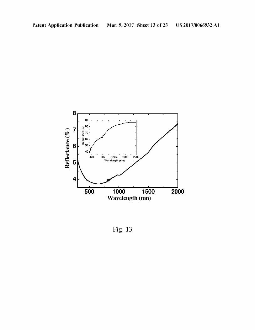
Mar. 9, 2017
I0132 FIG. 3. (a) Light absorption spectrum and (b) light reflectance spectrum (NIR range) of CNT-binder formula tion coated on aluminum Substrate according to Example 2 of the present disclosure. (0.133 FIG. 4. (a) Light reflectance spectrum (VIS-NIR range) and (b) Light reflectance spectrum (NIR range) of CNT-binder formulation coated on aluminum substrate according to Example 3 of the present disclosure. 0.134 FIG. 5(a). Light absorption spectrum of CNT binder formulation coated on aluminum Substrate according to Example 4 of the present disclosure. I0135 FIG. 5(b). Adhesion test of CNT-binder formula tion coated on aluminum Substrate according to Example 4: the tape (left) and the coating (right) after the test. (0.136 FIG. 6. Light reflectance spectrum (VIS-NIR range) of CNT-binder formulation coated on aluminum Substrate according to Example 7 of the present disclosure. I0137 FIG. 7. Light reflectance spectrum (VIS-NIR range) of CNT-binder formulation coated on aluminum Substrate according to Example 8 of the present disclosure. 0.138 FIG. 8. Light reflectance spectrum (IR range) of CNT-binder formulation coated on aluminum substrate according to Example 9 of the present disclosure. I0139 FIG.9. Scheme illustrating the fabrication of CNT/ ITO coating on Al substrate. (O140 FIG. 10. SEM images of (a) CNT, (b) CNT/ ITO'P'er, and (c) CNT/ITO'Pre coatings. 0141 FIG. 11. EDS spectra of (a) CNT, (b) CNT/ITO 'P'er, and (c) CNT/ITO'Pred coatings. 0142 FIG. 12. XRD pattern of CNT, CNT/ITOP' CNT/ITO'Pre coatings. 0143 FIG. 13. Reflectance spectra of CNT coating on Al substrate. Inset shows the reflectance spectra of Al substrate alone (no coat). 0144 FIG. 14. Reflectance spectra of CNT/ITOP' and CNT/ITOP' coatings. 0145 FIG. 15. (a) Variation of absorptance and emittance with the ITO layer thickness and (b) reflectance spectra of CNT/ITOP' coatings with varying thickness of ITO layer. 0146 FIG. 16. Sheet resistance of CNT/ITOP' coat ings with varying thickness of ITO layer. 0147 FIG. 17. Adhesion tests of: (a) CNT, (b) CNT/ ITO'P'er, and (c) CNT/ITO'Pre coatings. 0148 FIG. 18. Absorptance and emittance of CNT/ITO “"coating at: (a) different temperature at 6hr of time and
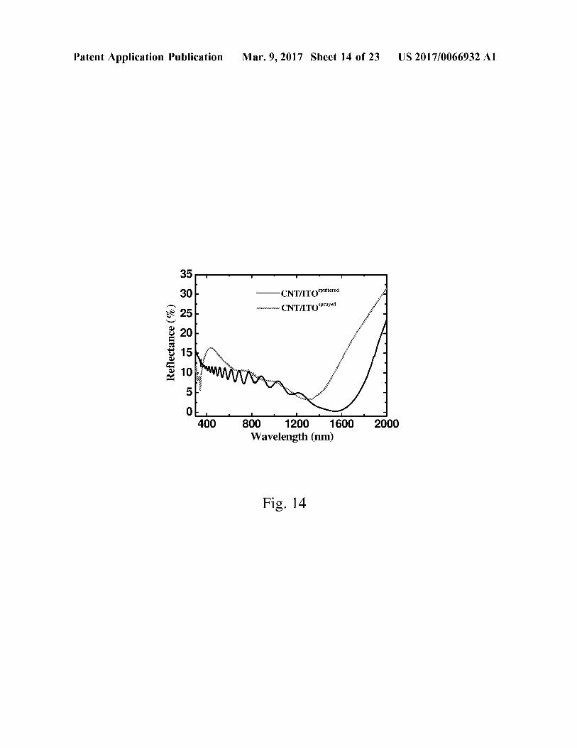
(b) different time at 250° C. 0149 FIG. 19. Scheme illustrating the fabrication of inverse tandem absorbing coating CNT/ITO in solar spec trum region. (O150 FIG. 20. SEM images of different BT/binder coat ings (a) before curing and (b) after curing. 0151 FIG. 21. TGA-MS analysis of binder under thermal treatment. Curing starts after 200° C. with the release of —OH fragments and HO molecules from the binder matrix. 0152 FIG. 22. (a) Effect of BT and binder concentrations and (b) NC and binder concentrations on coating reflectance in the VIS range. (O153 FIG. 23. MWCNT (NC type) coatings, after cross cut and tape test. 0154 FIG. 24. Optical device internal piece before and after spray coating the MWCNT ink.
US 2017/0066932 A1
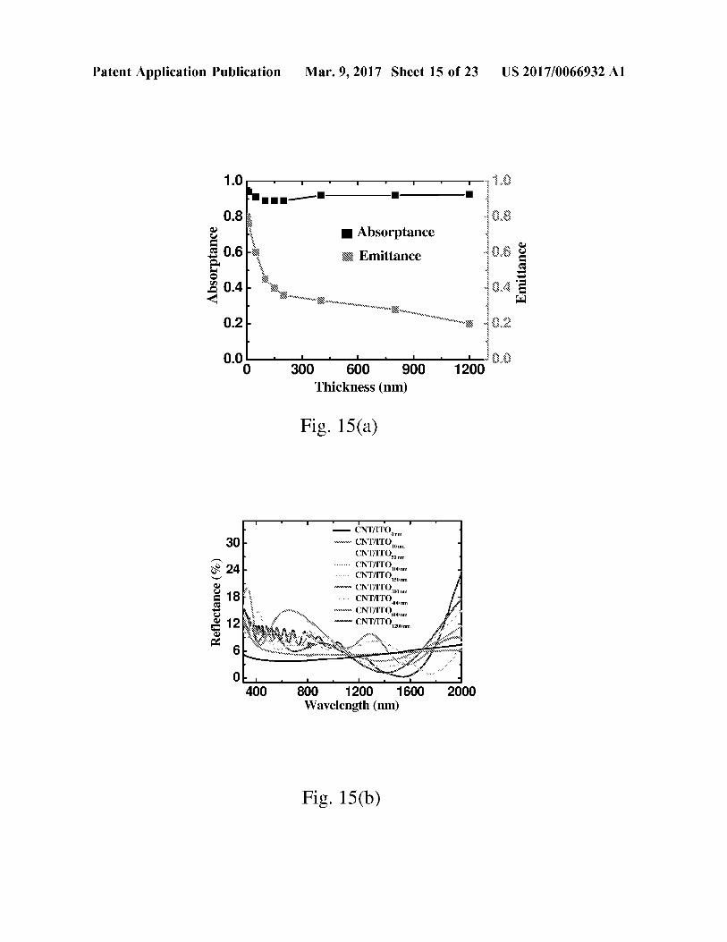
DETAILED DESCRIPTION OF EMBODIMENTS
Methods of Characterization of Coated Structures
Experimental Techniques
Structure and Morphology Characterization 0155 Structure and morphology were acquired using high resolution Scanning electron microscopy (HR-SEM, Sirion, XL30FEG) and stereo microscope (SQF II, China).
Compositional Analysis 0156 For compositional analysis, energy dispersive X-ray spectroscopy (EDX) measurements were performed. (O157 XRD measurements were performed with D8 Advance diffractometer (Bruker AXS, Karlsruhe, Germany) equipped with Göbel Mirror parallel-beam optics with CuKO. radiation (-1.54 A). Thickness Measurements
0158. Thickness of the coatings was measured with micro-TRI-gloss L (BYK Gardner GmbH, Germany)
Optical Measurements (Reflectance and Absorptance) 0159 Reflectance spectra were recorded with a CARY 5000 UV-visible-NIR spectrophotometer (Varian, USA). 0160 The absorptance of the coatings were calculated from the UV-vis-NIR reflectance spectra using the equation; C.+R+T=1, where C. is absorptance, R is reflectance, and T is transmittance. Since the coatings were fabricated on Al substrate, the transmittance is zero and therefore the absorp trance C=1-R. 0161 Emittance was measured with Emissometer AE1/ RD1 (Devices & Services Co, Dallas, Tex., USA).
Resistance Measurements
0162 Sheet resistance was measured with four-point probe Cascade Microtech (Beaverton, USA) coupled to an Extech milliohm meter (model 380562, Waltham, USA).
Spectral Selectivity
0163. In order to attain a tuneable spectral selectivity, coatings of ITO with different thicknesses were fabricated by Sputtering on top of the CNT coatings. 0164. Sputtering was carried out with FHR, Analgenbau GMBH, MS 75X4-L.
Adhesion Tests
(0165. The adhesion test was performed on both CNT coating as well as CNT/ITO coating prepared by both sputtering and spraying. The tests were conducted by Cross Cut-Tester 1 mm according to standards ASTM D 3359 and ISO 2409. In this test, a lattice pattern is cut into the coating penetrating through the Substrate. A tape is placed on the cut pattern and then pealed. The coating area is observed and the adhesion is rated in accordance with standard Scale.
Temperature Stability Tests
(0166 The performance evaluation of CNT/ITOP' coating was carried out by Subjecting them to heat storage in air at various temperatures and time durations. The absorp
Mar. 9, 2017
tance and emittance of the coatings were measured after cooling down to room temperature.
Materials and Methods of Preparation
Obtaining Absorbing Layer from CNT-Based Dispersion
Example 1
Coating Formed from Dimethylformamide (DMF)-Based Dispersion Comprising CNT and
Sires REN-60
Absorbing Layer Preparation (0167 500 mg of CNT (Baytubes cp70, Bayer Material Science, Germany) and 500 mg of 10% dispersing agent (Byk'77, Byk-Chemie GmbH, Germany) were mixed in 49 g of DMF (Merck). The mixture was sonicated for 20 minutes at 750 W in pulses of one second on and one second off. Then, 5 g of silicon resin Silres REN-60 (polysiloxane, Waker Chemie AG, Germany) was added to the dispersion and then the dispersion was sonicated for 5 minutes. The coating was prepared by spraying of the above dispersion on heated (100° C.) substrate. The samples were dried at 70° C. and then cured at 350° C. for two hours. 0.168. The liquid dispersion containing CNT and polysi loxane was converted into a heat-stable ceramic matrix upon curing. (0169. The absorbing black layer according the Example 1 coated on glass (left) and on aluminum Surface (right) achieved by wet deposition (spray coating) is displayed in FIG. 1(a). Adhesion Tests
0170 Adhesion test of the CNT-binder coating on alu minum according to Example 1 is displayed in FIG. 1(b). The tape (left) and the coating (right), after the test, is shown in the figure. The adhesion of the CNT coating on aluminum substrate according the Example 1 corresponds to ISO class 0. The edges of the cuts are completely smooth, and a cross cut area near 0% is affected.
Optical Measurements (0171 In the visible range (wavelength 380-750 nm) the absorbance reached over 96%. In the NIR, the absorption reached over 96% at the range of 700-1000 nm, over 94% at the range of 1000-1700 nm, and 93% at the range of 1700-2500 nm (displayed in FIG. 2(a)). 0172. The absorbing layer coated on aluminum substrate according to Example 1 exhibits high absorbance properties in the Vis-NIR range. The thickness of the coatings shows a very minor effect on the light absorption, decreasing from 96.94% in coatings with a thickness of about 1.9-2.1 um, to 95.90% in coatings with a thickness of 15-15.5 um (the results are summarized in Table 1).
TABLE 1.
The effect of coating thickness on the light absorption
% WS-NIR Coating Substrate absorption thickness
Glass 96.94% 1.9-2.1 lim Glass 96.72% 3.7-4.0 Im

US 2017/0066932 A1
TABLE 1-continued
The effect of coating thickness on the light absorption
% VS-NIR Coating Substrate absorption thickness
Glass 95.89% 6.5-6.7 m Glass 95.90% 15-15.5 m Aluminum 96.29% 1.9-2.1 um Aluminum 96.23% 3.7-4.0 m Aluminum 95.79% 6.5-6.7 m Aluminum 95.60% 15-15.5 m
0173 The absorbing layer coated on aluminum substrate according to Example 1 shows high performance in absorb ing NIR light in order to absorb and reduce the unwanted stray light in optical systems. The light reflected (R 96) reached less than 8% (wavelength range 3-10 um), particu larly reaching a low value of less than 2% at the wavelength range 3-5 um (displayed in FIG. 2(b)).
Example 2
Coating Formed from Dimethylformamide (DMF)-Based Dispersion Comprising CNT and
Silikophen P 80/MPA
Absorbing Layer Preparation
(0174 500 mg of carbon nanotubes (short MWCNT from Cheaptubes) and 500 mg of dispersing agent (Byk') were dispersed in 49 g dimethylformamide. The mixture was sonicated for 20 minutes at 750 W in pulses of one second on and one second off. 5g of the resin Silikophen P80/MPA was added to the dispersion and Sonicated for 5 minutes at 750 W in pulses of one second on and one second off. The coating was prepared by spray deposition on a heated aluminum substrate. The samples were dried on at 70° C. and then cured at 350° C. for two hours.
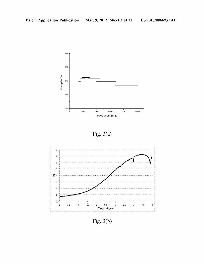
Optical Measurements (0175. In the visible range (wavelength 380-750 nm) the absorbance reached over 96%. In the NIR, the absorption was 96% at the range of 700-1700 nm and over 95% at the range of 1700-2500 nm (FIG. 3(a)). 0176 The coatings show high performance in absorbing NIR light in order to absorb and reduce the unwanted stray light in optical systems. The light reflected (R 96) reached less than 8% (wavelength range 3-8 um), particularly reach ing a low value of less than 3% at the wavelength range 3-5 um (FIG. 3(b)).
Adhesion Tests
0177. The CNT coating/aluminum adhesion corresponds to ISO class 0. The edges of the cuts are completely smooth, and a cross cut area near 0% is affected.
Temperature Stability Tests
0.178 The thermal stability was evaluated by storing the coating according to Example 2 at different temperatures (100° C., 200° C., 300° C., 400° C., 500° C) for 10 hours (displayed in Table 2). The coating showed good stability, maintaining the excellent adhesion and absorbance proper ties under all the conditions checked.
Mar. 9, 2017
TABLE 2
Thermal stability of the coating according to Example 2 at various storing temperatures (100° C., 200° C.,
300 C. 400 C., 500 C.) for 10 hours.
% Absorbance (360-740 nm)
(coating on aluminum % Absorbance (360-740 nm)
Temperature (coating on aluminum) with Surface treatment)
100° C. 95.36 O.O3 96.53 - 0.04 2OO C. 95.52 0.04 96.53 O.O3 300° C. 94.97 O.O3 96.57 O.O1 400° C. 95.39 O.O3 96.75 O.OS 500° C. 95.32 O.O2 94.69 O.39
0179 The stability was evaluated over a various storage period durations at 400° C. The coating according to Example 2 showed good stability, maintaining the excellent adhesion and absorbance properties under all the conditions checked. The absorbance properties, as a function of storage time, are shown in Table 3.
TABLE 3
Thermal stability of the coating according to Example 2 over storing temperature of 400° C. for 10, 20, 30,
40 and 50 hours.
Storage period % Absorbance (360-740 nm)
10 hours 95.39% O.O3 20 hours 95.35% O.OS 30 hours 95.39% O.O1 40 hours 95.42% 0.02 50 hours 95.51% 0.10
Example 3
Coating Formed from Dimethylformamide (DMF)-Based Dispersion Comprising CNT and
Sires REN-60
Absorbing Layer Preparation
0180 250 mg of carbon nanotubes (Nanocyl NC7000) and 500 mg of dispersing agent (Byk') were dispersed in 49 g dimethylformamide. The mixture was sonicated for 20 minutes at 750 W in pulses of one second on and one second off. 1.25 g of the silicon resin Silres REN-60 was added to the dispersion and sonicated for 5 minutes at 750W in pulses of one second on and one second off. The coating was prepared by spray deposition on aluminum Substrate. The samples were heated at 100° C. for 1 hour at a heating rate of 5°C/min, followed by heating to 300° C. for 30 minutes at a heating rate of 10° C./min, followed by heating to 350° C. for 30 minutes at a heating rate of 10° C./min.
Optical Measurements
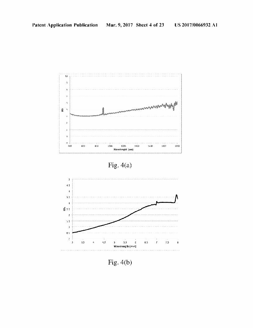
0181. The coatings show high performance in absorbing VIS and NIR light, thus enabling reduction of the unwanted stray light in optical systems. The reflected light (R 96) was about 4% in the VIS range (wavelength 380-750 nm) (FIG. 4(a)). In the NIR range (wavelength 3-8 um), the reflected light (R 96) was less than 3%, (FIG. 4(b)).

US 2017/0066932 A1
Adhesion Tests
0182 For the resulting coating the adhesion on aluminum corresponds to ISO class 0. The edges of the cuts are completely smooth, and a cross cut area near 0% is affected.
Example 4
Coating Formed from Water-Propylene Glycol Dispersion Comprising CNT and Alumina
Absorbing Layer Preparation 0183 200 mg of carbon nanotubes (Baytubes cp70) and 100 mg of a dispersing agent, Solsperse 46000, were dis persed in 15.7 g deionized water mixed with 4 g propylene glycol. The mixture was sonicated for 9 minutes at 750 W in pulses of one second on and one second off. 20 g of 10 wt % alumina solution (Disperal in water) was added to the dispersion and Sonicated for 5 minutes. The coating was prepared by spray deposition on aluminum Substrate. The samples were heated at 100° C. for 1 hour at a heating rate of 5°C/min, followed by heating to 300° C. for 30 minutes at a heating rate of 10° C./min, followed by heating to 350° C. for 30 minutes at a heating rate of 10° C./min.
Optical Measurements 0184. In the visible range (wavelength 380-750 nm) the absorbance of the CNT-binder coated on aluminum accord ing to Example 3 reached over 97%. In the NIR, the absorption could reach over 97% at a range of 700-1000 nm, over 96% at a range of 1000-1700 nm, and 95% at a range of 1700-2500 nm (displayed in FIG. 5(a)).
Adhesion Tests
0185. The CNT coating adhesion corresponded to an ISO class 3; the coating had flaked along the edges and/or at the intersection of the cuts. Across cut area between 5-15% was affected (FIG. 5(b)).
Temperature Stability Tests 0186 The thermal stability the coating according to Example 4 was evaluated by storing the coating at different temperatures (100° C., 200° C., 300° C., 400° C., 500° C.) for 10 hours (displayed in Table 4). The coating showed good stability, maintaining the adhesion and absorbance properties under all the conditions checked.
TABLE 4
Thermal stability of the coating according to Example 4 at various storing temperatures (100° C., 200° C.,
300 C., 400 C, 500 C.) for 10 hours.
% Absorbance (360-740 nm)
(coating on aluminum Temperature with surface treatment)
100° C. 97.26 O.OS 2OO C. 97.1 O.O14 300° C. 96.31 OO6 400° C. 97.88 O.OS 500° C. 97.88 O.O2
0187. The stability was evaluated for a longer period of time at 400° C. The coating showed good stability, main
Mar. 9, 2017
taining the adhesion and absorbance properties under all the conditions checked. The absorbance properties as a function of storage time are shown in Table 5.
TABLE 5
Thermal stability of the coating according to Example 4 over storing temperature of 400° C. for 10, 20, 30,
40 and 50 hours.
Storage period % Absorbance (360-740 nm)
10 hours 97.88% O.OS 20 hours 97.31% 0.16 30 hours 97.53% 0.08 40 hours 97.25% 0.13 50 hours 97.75% 0.04
Example 5
Coating Formed from Water-Propylene Glycol Dispersion Comprising CNT and Alumina Effect
of Coating Thickness on Absorptance
Absorbing Layer Preparation 0188 200 mg of carbon nanotubes (Baytubes cp70) and 100 mg of a dispersing agent, Solsperse 46000, were dis persed in 15.7 g deionized water mixed with 4 g propylene glycol. The mixture was sonicated for 9 minutes at 750 W in pulses of one second on and one second off. 2 g of 10 wit % alumina solution (Disperal in water) was added to the dispersion and Sonicated for 5 minutes. The coating was prepared by spray deposition on aluminum Substrate. The samples were cured at 100° C. for 1 hour at a heating rate of 5°C/min, at 300° C. for 30 minutes at a heating rate of 10°C/min, and at 350° C. for 30 minutes.
Temperature Stability Tests (0189 In the visible range (wavelength 380-750 nm) the coatings absorbance reached over 96%. The coatings thickness did not show any significant effect on the light absorption, remaining at around 96.31-97.19% for coatings where the thickness was about 1.7-5.6 um.
TABLE 6
Absorptance as a function of thickness of the coating according to Example 5 over storing temperature of
400° C. for 10, 20, 30, 40 and 50 hours.
Thickness (Lm) % Absorbance (360-740 nm)
1.774 - 0.104 96.31% 3.06 0.27 97.19% 5.61 - 0.35 97.08%
Example 6
Coating Formed from Water-Propylene Glycol Dispersion Comprising CNT and
Alumina-Methyltrimethoxysilane Effect of Coating Thickness on Absorptance
Absorbing Layer Preparation 0.190) 16 g methyltrimethoxysilane were mixed with 8 g of 10% alumina solution (Disperal in water). The mixture
US 2017/0066932 A1
was homogenized for 5 minutes at a speed of 13,000 rpm and kept at room temperature before use. 320 mg of carbon nanotubes Baytubes cp70 and 160 mg of dispersing agent, Solsperse 46000, were dispersed in 25.12 g deionized water mixed with 6.4 g propylene glycol. The mixture was soni cated for 9 minutes at 750 W in pulses of one second on and one second off. The alumina-methyltrimethoxysilane mix ture was added to the CNT dispersion and stirred for 2 hours. The coating was prepared by spray deposition on aluminum substrate. The samples were heated at 100° C. for 1 hour at a heating rate of 5°C/min, followed by heating to 300° C. for 30 minutes at a heating rate of 10° C./min, followed by heating to 350° C. for 30 minutes at a heating rate of 10° C./min
Optical Measurements
(0191). In the visible range (wavelength 380-750 nm), the coating absorbance reached over 96% (not shown here).
Adhesion Tests
0.192 The adhesion of CNT-binder based coating on aluminum substrate corresponds to ISO class 0. The edges of the cuts are completely smooth, and a cross cut area, near to 0%, was affected (not shown here).
Example 7
Coating Formed from DMF-Based Dispersion Comprising CNT and Silres REN-100
Absorbing Layer Preparation
(0193 250 mg of carbon nanotubes (Baytubes) and 500 mg of dispersing agent (Byk 9077) were dispersed in 49 g dimethylformamide. The mixture was sonicated for 20 min utes at 750W in pulses of one second on and one second off. 750 mg of the silicon resin Silres REN-100 was added to the dispersion and sonicated for 5 minutes at 750 W in pulses of one second on and one second off. The coating was prepared by spray deposition on a heated aluminum Substrate. The samples were dried on at 70° C. and then baked at 350° C. for two hours.
Optical Measurements
0194 The coatings show high performance in absorbing VIS and NIR light, thus enabling reduction of the unwanted stray light in optical systems. The reflected light (R 96) was >4.5% in the VIS range (wavelength 400-700 nm) (FIG. 6).
Example 8
Coating Formed from DMF-Based Dispersion Comprising CNT and Low Binder Content (Silres
REN-100) in Mixture
(0195 250 mg of carbon nanotubes (Baytubes) and 500 mg of dispersing agent (Byk 9077) were dispersed in 49 g dimethylformamide. The mixture was sonicated for 20 min utes at 750W in pulses of one second on and one second off. 250 mg of the silicon resin Silres REN-100 was added to the dispersion and sonicated for 5 minutes at 750 W in pulses of one second on and one second off. The coating was prepared
Mar. 9, 2017
by spray deposition on a heated aluminum Substrate. The samples were dried on at 70° C. and then baked at 350° C. for two hours.
Optical Measurements
0196. The coating according to Example 8 shows high performance in absorbing VIS and NIR light, thus enabling reduction of the unwanted Stray light in optical systems. The reflected light (R 96) was >4.0% in the VIS range (wave length 400-700 nm) (displayed in FIG. 7).
Example 9
Coating Formed from DMF-Based Dispersion Comprising CNT and Low Binder Content (Silres
REN-100)
(0197) 250 mg of carbon nanotubes (Baytubes) and 500 mg of dispersing agent (Byk') were dispersed in 49 g dimethylformamide. The mixture was sonicated for 20 min utes at 750 W in pulses of one second on and one second off. 3 g of the silicon resin Silres REN-100 was added to the dispersion and sonicated for 5 minutes at 750 W in pulses of one second on and one second off. The coating was prepared by spray deposition on a heated aluminum Substrate. The samples were dried on at 70° C. and then baked at 350° C. for two hours.
Optical Measurements
0198 The coating according to Example 8 shows high performance in absorbing VIS and NIR light, thus enabling reduction of the unwanted Stray light in optical systems. The reflected light (R96) was >2.5% in the IR range (wavelength 2.5-7 um) (FIG. 8). (0199 From the above examples, it is very clear that CNT absorbs solar light strongly and reflects weakly, thereby providing a Superior candidate for Solar light absorber. 0200. However, in solar energy conversion applications, the coating of CNT may suffer from radiative emissivity in the IR region which results in overheating of the layer of material serving as an absorbing Surface, and thus, in an increase of heat loss by convection, heat transfer and re emission of additional heat by the surface. 0201 A further testing of coating formulations in order to inhibit the radiative emission of CNT coating in the IR region and make this coating selective for Solar-thermal conversion is described in the following examples. This approach includes modifying the type of the binder, the ratio between the binder and CNT, forming a concentration gradient of the CNT throughout the deposited layer and adding an additional coating layer below or on top of the CNT absorbing layer. The layers may be different coating formulations for each layer, or by combining several func tional additives within one or more coating layer. 0202 Without being bound by theory, the emissivity of the CNT coating depends on the type of the binder used in the formulation process. Al-O, trimethoxymethyl silane, and Ren 100 (resulting in silica and silicon containing polymers) were tested as binders and Baytube and Nanoyl tube were tested as absorbing materials.

US 2017/0066932 A1
Example 10
Coating Formed from Water-Propylene Glycol Based Dispersion Comprising Baytube CNT, Al-O
and Trimethoxymethyl Silane 0203. In the first step, 0.06 g of solsphere 46000, 0.12g of baytube CNT, 4 g of propylene glycol, and 15.82 g of water are mixed in a 28 ml vial and Sonicated for 3.5 min at 750 W with amplitude of 85% and in pulse of one second on and one second off. (0204. In the 2" step, binder was prepared by mixing 2 g of 10%. Al-O and 1 g of trimethoxysilane and stirred for 2.5 hr at 820 rpm. (0205. In the 3" step, 0.1 g of Byk333, 1.25g of binder from the 2" step and 8.75 g of CNT dispersion from the 1 step are mixed and stirred for 5 hr at 820 rpm. The coating was prepared on an Al Substrate by spraying of the mixture obtained from the 3" step and then heated in an oven at 100° C. for 30 min with rate of 5°C/min, then at 250° C. for another 30 min with rate of 10° C./min and then finally at 350° C. for one hour with the rate of 10° C./min. 0206. The coating exhibited emissivity in the range of O.87-088.
Example 11
Coating Formed from Dispersion Comprising Nanocyl CNT and REN 168
0207 1 g Byk 9077 was mixed in 10% DMF solution, 0.1 g of nanocyl CNT and 18 g of DMF in a 28 ml vial and sonicated for 10 min at 750 W with amplitude of 85% and in pulse of two second on and one second off. After sonication, 6 g of REN 168 of 10% DMF solution was added to the mixture and sonicated in bath Sonicator for 10 min. The coating was prepared by spraying the formulation on a heated Al substrate and then heated in oven at 350° C. for 2 hr. 0208. The coatings exhibited emissivity in the range of 0.77-0.78.
Example 12
Coating Formed from Dispersion Comprising Baytube CNT and REN 168
0209 2 g of Byk 9077 was mixed with 10% DMF solution, 0.2 g of baytube CNT and 18 g of DMF in a 28 mL vial and sonicated for 10 min at 750 W with amplitude of 85% and in pulse of two second on and one second off. After sonication, 6 g of REN 168 of 10% DMF solution was added to the mixture and sonicated in bath Sonicator for 10 min. The coating was prepared by spraying the formulation on a heated Al substrate and then heated in oven at 350° C. for 2 hr. 0210. The coatings show the emissivity in the range of 0.77-0.78. 0211. As appreciated from Examples 10-12, REN 168 binder decreases the emissivity by 12% in comparison to Al-O and trimethoxymethyl silane as binder. 0212. Without being bound by theory, the decrease in emissivity in the case of REN 168 may be due to its inherent IR reflective property compared to Al-O and trimethoxym ethylsilane mixture. These results indicate that changing the type of binder may affect the emissivity of the coating.
11 Mar. 9, 2017
Example 13
Gradient Absorbent Layer Coating Formed from Dispersion Comprising CNT and Ren 100
0213. Additional approach to decreasing the emissivity according to the present disclosure is by providing a gradient coating on a substrate. The 1 layer comprises 1:3 (wt %/wt %) ratio of CNTs and REN 168. A 2' and 3 layer comprises 1:2 and 1:1 (wt %/wt %) of CNTs and REN 168 was coated on the 1 layer. 0214 Example 13 was prepared using the same proce dure as in the case of Example 12, only with the change in the amount of Ren 100. For 2" layer, 4 g of Ren 100 and for 3" layer, 2 g of REN 168 was used. 0215. The coatings show emissivity in the range of O.73-O.74. 0216. As appreciated from Example 13 (gradient layer) in comparison with Example 12 (non-gradient layer), there is a decrease in the emissivity of gradient coating of CNT compared to only one layer of coating.
Obtaining Transparent Conducting Layer on Absorbing Layer Comprising CNT-Binder Matrix
Example 14
Transparent Conducting Layer Coating on Absorbent Layer
0217. Additional approach is to use a layer which is transparent to Solar region but reflects light in the IR region on the layer on top of the CNTs coating. Such materials, which are transparent in the Solar region but reflect light in the IR region, may significantly reduce the radiative emis sion in the IR region. A material with wide band gap, may reflect light in the IR region. The wide band gap materials may include: SnO, In,O. In doped SnO, (ITO), Sb doped SnO (ATO), CdSnO, SiC. GaN, AlN, BN, Hf, LaB, etc. 0218. Among these materials, SnO, InO, ITO, and ATO as top layer coating was tested. However, this approach can be applied with various materials that have the suitable band gap and refractive index. 0219. This coating was carried out by spray coating or sputtering of formulations containing nanoparticles or pre cursor for the required material and by Sputtering process. The coating thickness can be controlled according to the applied deposition method, to yield the minimal emissivity. 0220 ITO is a candidate for top layer coating because of
its stability at high temperature, high carrier concentration, and low sensitivity to moisture. 0221) ITO Coating by Sputtering: 0222. The coating of ITO with different thickness on top of the CNT layer was performed by magnetron sputtering for various durations and the samples are termed CNT/ITO'" tera.
0223 ITO Coating by Spraying: 0224 First, 0.08 g of Sn(acac)C1, was dissolved in 8 ml of DMF. To this solution, 0.8 g of In?acac), and 0.2 ml of HCl (concentrated) was added and stirred for 2 hr. Then 0.1% of Byk'77 was added to the reaction mixture and stirred for another 20 min 1-1.5% of silicon resin Silres REN-168 was added to the mixture and stirred for another 10 minute. The reaction mixture (2 ml) was sprayed on the CNT layer, which was heated to 120° C. The sample was
US 2017/0066932 A1
annealed at 450° C. in air for 40 min and then under N for 1 hr. These coatings are termed CNT/ITOP'. 0225. In the 1 step CNT coating was prepared according to the procedure of Example 12 and then in the 2" step, coating of ITO of 10, 50, 100, 150, 200, 400, 800, and 1200 nm thickness on CNT coating was fabricated by Sputtering process.
0226 O.8-02.
The coatings show emissivity in the range of
Example 15
Transparent Conducting Layer Coating on Absorbent Layer Comprising Baytubes CNT and
REN-168 (Polysiloxane) as Binder
0227 0.2 g of CNT (Baytubes cp70) and 2.0 g of 10% dispersing agent (Byk') were mixed in 17.8g of DMF. The mixture was sonicated for 10 minutes at 750W in pulses of two second on and one second off and amplitude of 85%. Then, 6.0 g of 10% silicon resin Silres REN-168 (polysi loxane) was added to the dispersion and bath Sonicated for 5 minutes. The coating was prepared by spraying 3 ml of the above dispersion on heated (120° C.) Al substrate, with area of 5x5 cm. The samples were cured in an oven at 350° C. for two hours.
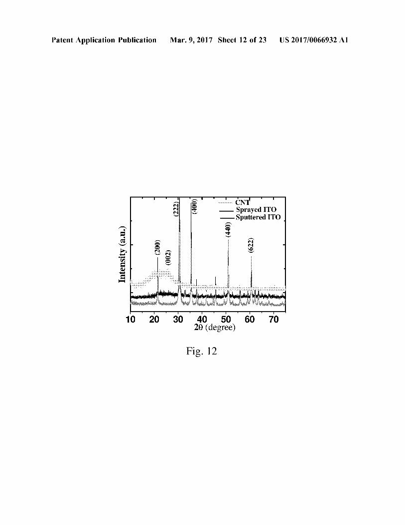
0228 FIG. 9 illustrates the fabrication of CNT/ITO coat ing on Al substrate. The first layer composed of CNT and binder involves spraying of the liquid dispersions of CNT containing polysiloxane, which is converted into a heat stable ceramic matrix upon heating. The second layer is composed of ITO, which is deposited on the CNT layer by spraying or Sputtering. 0229. The coatings were characterized by SEM, EDX, and XRD. FIG. 10 shows the SEM image of a typical CNT coating. From the image (FIG. 10(a)) it is observed that the diameter of the CNT is in the range of 23-28 nm. The EDS measurement (FIG. 11) shows the signature of C from CNT and Si and O from the polysiloxane binder. 0230. The thickness of the coatings was determined as 2-3 um using micro-TRI-gloss LL. 0231. The XRD pattern of CNT coating also shows the signature of CNT at 20 of 25 corresponds to the (002) plane (FIG. 12). FIG. 10 (b) presents SEM image of ITO coating of thickness of 1.2 Lum on CNT coating prepared by sput tering. From the image, it is observed that ITO particles are crystalline and have triangular structure with an average size of 500 nm. The EDS analysis (FIG. 11) shows the signature of only Sn, In, and O. There is no signature of C from CNT coating which implies that the coating of ITO on CNT is uniform. The XRD pattern also shows the signature of ITO which is associated with the (200), (222), (400), (440), and (622) planes (FIG. 12). 0232 FIG. 10(c) shows SEM image of CNT/ITOP' coating. From the image, it is observed that particles are crystalline and have polyhedral structure with size in the range of 200 to 500 nm. The thickness of the film measured by micro-TRI-gloss LL was estimated as 1.1 to 1.5 Lum. The EDS analysis (FIG. 11) shows the signature of Sn, In, and O from ITO and Si from polysiloxane. It should be noted that there is a signature of C in the EDS spectrum. The XRD pattern also shows the signature of ITO as in the case of sputtered ITO (FIG. 12).
Mar. 9, 2017
Absorptance and Emittance Measurement
0233. As noted above, the absorptance of the coatings were calculated from the UV-vis-NIR reflectance spectra using the equation; C+R+T-1, where C. is absorptance, R is reflectance, and T is transmittance. Since the coatings were fabricated on Al Substrate, the transmittance is Zero and therefore the absorptrance C=1-R. FIG. 13 shows the reflec tance spectra of Al substrate and CNT coating on Al Sub strate. From the inset of the figure, it is observed that Al Substrate has very high reflectance in the Solar spectrum region. The absorptance in the region of 0.3 um to 2 um was calculated as 0.267 (FIG. 13, inset). In case of CNT coating, it has one reflectance minima at 600 nm having a reflectance of 3.7% (FIG. 13). Thus, the coating has high absorptance of 0.963 at 600 nm. The absorptance in the main part of the solar spectrum region (450-700 nm)7 is 0.962 (FIG. 13) and the total absorptance of the coating in the full solar spectrum region of 0.3 um to 2 um was calculated as 0.945 (FIG. 13). 0234. From the absorptance measurement, it is appreci ated that CNTs absorb solar light strongly and reflect weakly, which make them Superior candidate for Solar light absorber. In spite of these advantages, the coating of CNT, suffers from low selectivity and radiative emission in the IR region. The CNT coating shows emittance of 0.8 (Table 7). Attempts have been made to inhibit the radiative emission of CNT coating in the IR region by coating with material, which is transparent to Solar region but reflects light in the IR region, on top of the CNT coating. Inverse tandem absorbing materials are transparent in the Solar region but reflect light in the IR region, and significantly reduce the radiative emission in the IR region. 0235. As noted above, ITO as a candidate for top layer coating because of its stability at high temperature, high carrier concentration, and low sensitivity to moisture. FIG. 14 shows the reflectance spectra of a CNT/ITO" coating having a 1.2 um of ITO top layer and CNT/ ITO' coating having a coating of sprayed ITO with an average thickness of 1.3 um. It is seen that the CNT/ ITO" coating has a reflectance minima at 1540 nm having reflectance of 0.3%. Thus, the coating has the absorp tance of 0.997 at 1540 nm. The absorptance of CNT/ ITOP' coating in the NIR region (1300-1700 nm) is 0.988. This increase in absorptance of CNT/ITO'P' coating in the region of 1300-1700 nm may be due to the antireflecting property of ITO in that region. The total absorptance of the coating in the full Solar spectrum region of 0.3 um to 2 um is 0.927. The emittance of the coating was ca. 0.2 (Table 1). Hence, adding a coating of ITO of 1.2 um thickness on top of a CNT coating significantly decreases the emittance while only slightly affects the absorptance. The reflectance spectra (FIG. 14) of CNT/ITO' coating has a reflectance minima at 1300 nm having a reflectance of 3.1% and an absorptance of 0.969. The absorptance of CNT/ITOP' coating in the NIR region (1100-1450 nm) is 0.956 and in the full solar spectrum region of 0.3 um to 2 um is 0.878 (FIG. 14). The emittance of the coating was ca. 0.3 (Table 7). 0236 Without being bound by theory, this lower absorp tance and higher emittance of CNT/ITO' coating as compared with CNT/ITO" coating may be due to the lower transmittance of ITO layer prepared by the spray method.
US 2017/0066932 A1
TABLE 7
Absorptance, emittance and adhesion properties of samples with and without CNT coating and ITO coating.
Sample Absorptance Emittance Adhesion
Al O.267 O.O6 AfCNT O.945 O.8 95% AONT/ITOSPuttered O.927 O.2 >95% AONT/ITOSProved O.878 O.3 35-65%
Spectral Selectivity and Resistivity Tests
0237. In order to attain a tuneable spectral selectivity, coatings of ITO with different thicknesses were fabricated by sputtering on top of the CNT coatings. FIG. 15(a) and FIG. 15(b) show the variation of absorptance and emittance of CNT/ITO" coating with the thickness of ITO coat ing. From FIG. 15(b), it is evident that the spectral selec tivity of the absorbing coating is highly sensitive to the thickness of ITO layer. With the increase in the thickness of ITO, both the absorptance and emittance decreased up to the thickness of 0.2 Lum. At 0.2 Lum of thickness, the absorptance was 0.89 and emittance was 0.36. For coatings with thick ness >0.2 Lum the emittance decreased continuously with increasing the thickness of ITO but the absorptance started to increases. At 1.2 Lum thickness, the emittance decreased to 0.2 whereas the absorptance increased to 0.927. With increase in the thickness of the ITO, there is a decrease in sheet resistance (displayed in FIG. 16) and hence there is an increase in the number of free electrons which is responsible for the IR reflectivity and thus decreases the emittance. 0238. Without being bound by theory, the change in the absorptance of the coating with thickness of ITO is due to the change of the refractive index of ITO with the thickness.
Adhesion Test
0239. It can be seen from Table 7 and FIG. 17(a) that the adhesion of the CNT coating is very good (95%) and the Scotch tape does not remove the coating. By this tape test, ~5% of the coating was removed. High adhesion is achieved since the CNT in the resulting coating are embedded within a matrix, which by itself has good adhesion to metallic and other Substrates. The coating had flaked along the edges and/or at the intersection of the cuts. The CNT/ITOP' coating shows excellent adhesion of >95% (FIG. 17(b)) as less than 5% of the coating was removed by the tape test. On the hand, the CNT/ITOP' coating shows moderate adhe sion of 35-65% (FIG. 17(c)) as >50% of the coating was removed by the tape test.
Stability of the Coat at High Temperature in Air
0240. The thermosolar absorbers should operate at high temperatures, and therefore, heat stability was further evalu ated. As displayed in absorptance, emittance and adhesion measurement in Table 7, CNT/ITO'" shows better performance than that of CNT/ITOP'. Thus, the perfor mance evaluation of only CNT/ITO" coating was carried out by Subjecting them to heat storage in air at various temperatures and time durations. The absorptance and emittance of the coatings were measured after cooling down to room temperature. FIG. 18(a) shows the absorp tance and emittance measurements for samples Stored at
Mar. 9, 2017
various temperatures for 6 hrs. From FIG. 18(a), it is observed that there is no noticeable change in the value of absorptance and emittance up to 200° C. At 300° C., slight increase in both absorptance and emittance occurred, lead ing towards lower spectral selectivity (0.934/0.24). The long term stability of the coating was evaluated at 250° C. and it shows very good spectral selectivity of 0.938/0.25 even after 100 hr (FIG. 18(b)). After 100 hr, there was a slow decrease in the spectral selectivity due to slow increase in emittance of the coating and after 7 day the spectral selectivity was 0.938/0.27. This decrease in spectral selectivity may be due to the oxygen adsorption on ITO layer as the heating was carried out in air. Due to the adsorption of oxygen, the free electrons which are responsible for IR reflectivity may be trapped. This was verified since the spectral selectivity was recovered by annealing the coating in N at 450° C. for 1 hr. During annealing under N2 at high temperature, the adsorbed O. was removed. As a result, trapped electrons become free and reflect IR light. After 7 day of heating at 250° C., the adhesion test was performed, resulting in very good adhesion of 95%. 0241 Fabrication of inverse tandem absorbing coating CNT/ITO with excellent spectral selectivity has been dem onstrated. As shown in FIG. 19 the CNT layer shows low reflectance in the Solar spectrum, functions as an excellent solar absorber and the ITO layers which show higher reflec tance in the IR region, function as emittance inhibitor and make the absorbing coating spectrally selective. Conclusions
0242. In summary, the examples of the present disclosure display a new approach whereby the final spectrally selec tive solar thermal coating CNT/ITO is formed as a continu ous and uniform layer which combines the absorber layer of CNT prepared by spraying and IR reflecting layer of ITO prepared by sputtering on top of the CNT coating. The coating exhibits excellent spectral selectivity with high absorptance of 0.927 and low emittance of 0.2. The depo sition of ITO on CNT coating decreases the emissivity by at least 20% compared to that of without ITO coating. 0243 Without being bound by theory, this decrease is due to the IR reflective property of ITO which reflects back the emitted heat towards the absorbing materials. The emissivity may be controlled by varying parameters such as the coating material or combination of several materials, the thickness of this layer, and matching properly the refractive index of the top coating. 0244. The coating shows superior adhesion of >95% and high thermal stability up to 250° C. with very good selec tivity even after 100 hr. The spectral selectivity can be tuned by varying the thickness of the ITO layer. The developed system shows promising results for future applications as Solar thermal energy conversion.
Absorbent Layer Coating for Reducing Stray Light Example 16
Coating Formed from Dispersion of DMF Comprising MWCNT and SILRES REN 168
Binder Evaluation of the MWCNT:Binder Ratio Effect
Materials and Methods
0245. Two multi-walled carbon nanotube (MWCNT) coating formulations were used: (1) Baytubes(R C70 P
US 2017/0066932 A1
(Bayer MaterialScience, Germany) characterized by a purity of N99%, a diameter of 13-16 nm and a length of 1-10 um and (2) NC7000 (Nanocyl, Belgium) characterized by a purity of N90%, a diameter of 9.6 mm and a length of 0.5-2 um. The starting coating formulations were composed of MWCNTs (0.5 wt.%), dispersing additive BYK9077 (1 wt. %) (Byk-Chemie GmbH, Germany) and dimethylforma mide (DMF) (98.5 wt.%) (Biolab, Israel). 0246 The formulations were prepared using a horn soni cator (model Vibra-Cell, Sonics & Materials Inc., USA) for 20 min at 640 W. The samples were cooled in an ice water bath during the Sonication process. This starting formulation was mixed at various ratios with a silicon-based binder. A binder solution was prepared by dissolving SILRES(R) REN 168 (0.5 wt.%) (Waker Chemie AG, Germany) in DMF. The final coating formulation was prepared by mixing the MWCNT dispersion and the binder solution at several ratios. The substrates and aluminum plates (1 mm 50 mm 50 mm size) were degreased by Sonication in an acetone bath for 5 min. The coatings were formed by airbrush spraying 20 g of the coating solution onto heated aluminum plates (70° C.). The coated samples were further baked at 350° C. for 120
1.
0247 The binder curing process was studied by TGA-MS analysis (40-350° C., in a heating rate of 10°C/min), using a STA TG-DSC 449 F3 Jupiter(R) instrument (NETZSCH, USA). 0248. The diffuse reflectance of the coatings was mea sured in the VIS-NIR range (350-2400 nm) using a Cary 5000 spectrophotometer instrument (Varian, USA). Coating thickness was measured using a micro-TRI-gloss LL instru ment (BYK Gardner GmbH, Germany).
Results
0249 Black coatings were formed by spraying a constant amount of the coating formulation on an aluminum plate pre-heated at 70-100° C. The performance of the resulting coatings was evaluated by measuring the light reflectance (% R) in the range of 350-2400 nm To ensure a good adhesion of the black coating to the aluminum Substrate, each formulation contains, in addition to the MWCNT as the absorbing material, a heat resistant binder, at various weight ratios. The evaluation of the effect of MWCNT: binder ratio was performed with coatings with a similar thickness, 2-3 um. The measurements were also conducted for a formula tion without a binder, and for a formulation with a binder
Mar. 9, 2017
only. After performing the spray coating, the resulting wet coatings were dried to evaporate the solvent, followed by baking at 350° C. for 2 h, to convert the binder into a ceramic matrix. The coating morphologies before and after baking are shown in FIGS. 200a) and 200b). As seen, prior to the thermal treatment there is a layer of the organic binder on top of the CNTs, while after baking this layer is partly removed, clearly showing the presence of entangled MWCNTs. 0250. The thermal process for the binder curing process was studied by TGA-MS analysis. The binder material consists of siloxane chains with silanol end groups. During heating, the siloxane chains are cross linked by the conden sation of —OH groups (releasing H2O). It was found (FIG. 21) that the curing process starts at 200° C. At this tem perature, as found by the MS, the decrease in the mass is due to the release of the –OH fragments and H2O molecules.
Optical Measurements
0251. The reflectance of the coatings obtained by spray ing was measured at the VIS-NIR range, and is presented as a function of wavelength (FIGS. 22(a) and 22(b)), and also as the calculated integral of reflectance (% Rio) at each range: % R for 350-800 nm and % R, for 850-2400 nm (Table 8). The coating experiments were conducted with two types of CNTs, 1-10 um long, Baytubes(R C70 P (BT), and 0.5-1.5 um long, Nanocyl 7000 (NC). (0252) In the VIS range (350-800 nm) aluminum plates have the integral of reflectance % R=59.87 (+3.35)%. After coating the substrate with the binder solution without CNTs, the reflectance slightly decreases up to % R=45.79(+10. 98)%. The reflectance decreases significantly while using the coating formulations with the two types of MWCNTs: Coatings composed of 7% MWCNT/binder 93% has % R=5.11 (+0.04)% (for BT type) and % R=5.05 (+0.04)% (for NC type). A further decrease of% R was found, as the concentration of the MWCNT in the coating increased, reaching a minimum value of % R=2.60(+0.01)% for BT and 2.82(+0.02)% for NC with coating composed of 100% MWCNT only (without binder). (0253) In the NIR range (850-2400 nm), all the reflectance values were in the range of %. R=4-6.5, however the dependence on MWCNT concentration was not very sig nificant. It should be noted that at this range, the longer CNT tubes (BT) were slightly better than the shorter ones (NC). about 1% difference in reflectance value.
TABLE 8
Integral of reflectance in VIS (% R1) and NIR (% R2) ranges of BT and NC coatings with various MWCNT-binder ratios.
Coating composition MWCNT:binder
100%:0% 85%:15% 71%:29% 57%:43% 43%:57% 29%.71% 15%:85%
BT NC
% R. % R2 % R. % R2 350-800 mm 850-2400 mm 350-800 nm. 850-2400 mm
2.60% (+0.01) 2.75% (+0.01) 3.18% (+0.06) 3.67% (+0.00) 4.29% (+0.01) 4.44% (+0.03) 4.56% (+0.05) 5.11% (+0.04)
4.05% (+0.06) 3.93% (+0.06) 4.22% (+0.11) 4.50% (+0.12) 5.20% (+0.10) 4.61% (+0.11) 4.93% (+0.11) 5.94% (+0.23)
2.82% (+0.02) 2.95% (+0.04) 3.04% (+0.08) 3.33% (+0.06) 3.51% (+0.04) 3.54% (+0.00) 4.86% (+0.04) 5.05% (+0.04)
5.41% (=0.32) 5.45% (+0.07) 5.45% (+0.09) 5.55% (+0.03) 5.50% (+0.13) 5.13% (+0.02) 5.59% (+0.14) 6.53% (+0.42)
US 2017/0066932 A1
TABLE 8-continued
Mar. 9, 2017
Integral of reflectance in VIS (% R1) and NIR (% R2) ranges of BT and NC coatings with various MWCNT-binder ratios.
BT
Coating composition MWCNT:binder
% R. 350-800 mm
% R2 850-2400 mm
% R. 350-800 mm
O%:100% 45.79% (+1.98) 75.89% (+1.80) A1 only 59.87% (+3.35) 80.33% (+4.58) 59.87% (+3.35)
Adhesion Tests
0254 The adhesion of the coatings to the aluminum substrates was evaluated by two standard tape test with cross-cut, in which the adhesion is rated according to the fraction of detached coating, and classified according to a standard scale. The adhesion results are presented in Table 9 according to ISO 2409 (0 grade is the best, without detached coating, grade 5 is the worst, above 65% detach ment), and according to ASTM D3359 (5B grade is the best, without detached coating, OB is the worst, above 65% detachment). 0255 Coatings with a high content of MWCNT (>85%) but with low binder concentration (<15%) presented a poor adhesion (class 3; class 2B) (typical adhesion results are presented in FIG. 23). The adhesion is improved while increasing the binder concentration: good adhesion was achieved in samples containing 29-71% MWCNTs and 71-29% binder (class 2; class 3B). Excellent adhesion was observed in samples where the binder concentration was >85% (class 0; class 5B). 0256 Two types of nanotubes (short and long) were used
to form two series of MWCNT: binder coatings. 0257. It was expected that the longer nanotubes would form a more entangled and dense net structure compared to the short tubes. This difference in morphology could provide a higher cohesion force and interaction between the tubes, resulting in a higher adhesion to the Substrate. However, on the contrary, it is interesting to note that the adhesion is affected only by the binder concentration while it is not affected by the length of the MWCNT.
TABLE 9
Adhesion classification of different CNT coatings according to ASTM and ISO standard methods.
Coatings After thermal as prepared cycling test
ASTM ASTM MWCNT:binder D3359 ISO 2409 D3359 ISO 2409
100%:0% Class 2B Class 3 Class OB Class 5 85%:15% Class 2B Class 3 Class OB Class 5 71%:29% Class 3B Class 2 Class 3B Class 2 57%:43% Class 3B Class 2 Class 3B Class 2 43%.57% Class 3B Class 2 Class 3B Class 2 29%:71% Class 3B Class 2 Class 3B Class 2 15%:85% Class SB Class 0 Class SB Class 0 7%:.93% Class SB Class 0 Class SB Class 0
Temperature Stability Tests 0258 Black coatings for stray light reduction may be used not only in conventional optical devices (operating in
45.79% (+1.98)
NC
% R2 850-2400 mm
75.89% (+1.80) 80.33% (+4.58)
the terrestrial conditions) but also in space applications (for e.g. satellites). For both applications, coatings may be exposed to high temperatures due to the proximity with high heat dissipating parts, where the temperature is likely to go around 200° C. for long periods. In space applications, black coatings in satellites are exposed to low temperatures when present in the shadowed area. 0259. Thermal cycling test is performed in order to simulate space environment. The European Space Agency standard (ESA ECSS-Q-70-04A, 2008) recommends to per form 100 cycles of cooling (-100° C.) and heating (100° C.) of samples under low pressure (10 Pa) with a dwell time of at least 5 min In this work we used a different protocol with higher and lower temperatures: The thermal test was performed for high temperature stability (by heating the coatings at 200° C. for 2 h) and for low temperature stability (by dipping the coatings in liquid N for 2 h). In this research we aimed at showing that the high absorbing black coatings are stable at very high and very low temperatures. 0260 Thermal cycling test was performed by dipping the samples in liquid N. (-196° C.) for 5 min, bringing them to room temperature for 5 min and introducing them into an oven at 200° C. for 5 min. This cycle was repeated 10 times. 0261. After thermal tests, the coatings were examined visually for morphological damage (by an optical micro scope), for optical properties (% R) and for adhesion (by cross-cut and tape test). 0262. It was found that the samples showed a good stability at high temperature, coating flaking was not observed, and the optical and adhesion properties remained similar before and after the test. The thermal test at low temperature showed different results. Although optical prop erties were retained after the tests and there was no visual indication for damage, it was found that there was a dete rioration in the adhesion of the samples rich in CNT com pared to the binder. The failure was observed for samples having 85% MWCNT and above. Adhesion of such samples decreased from ASTM class 2B/ISO class 3 to ASTM class OB/ISO class 5. The same results were observed after the thermal cycling test (Table 9), probably due to the lack of the binder at these concentrations of CNTs.
Coating Complex Structures 0263. The method proposed in the present disclosure provides a simple and low cost approach for producing non-reflective, high light-absorbing coatings by wet depo sition of CNTs. This method provides a coat on 3D struc tures in a very short time, where the black coating is required in complexes and relatively large areas. FIG. 24 shows an internal piece of an optical device before and after coating with the CNT-based formulation according to the present invention.
US 2017/0066932 A1
Conclusions
0264. Highly absorbing black coatings composed of MWCNT can be formed by a very simple and low cost formulation. CNTs are dispersed in surfactant solution of DMF and then mixed with a silicon based binder solution. The coatings are obtained by various simple wet deposition methods. Such as spray coating, dipping, painting, coil coating and bar coating, which allows coating flat and complex 3D structures. 0265. The adhesion properties are controlled by the MWCNT/binder concentration. Increasing the binder con centration the adhesion is improved. The optimal ratio MWCNT/binder for a satisfactory adhesion should be evalu ated in view of the final application requirements. 0266 The binder/CNT ratio affects significantly the opti cal properties of coatings. The reflectance in the VIS range decreases when decreasing the binder/CNT ratio. It should be noted that the research was focused mainly on black coating for visible light absorption, which consists the main optical noise (stray light) in optical instruments. It was found that such coatings also provide a low reflectance in the NIR range. 0267 All the coatings showed an excellent stability at high temperature, while maintaining their optical and adhe sion properties. At very low temperature, the samples main tained their optical properties, but the adhesion was dete riorated in coatings containing low binder concentration.
1.-74. (canceled) 75. A light-absorbing element coated on at least a region
of its surface with a film of at least one light-absorbing material, the light-absorbing material being associated with at least one binder material, the film being between 1 and 20 um thick and having light absorption of at least 90%.
76. The element according to claim 75, for stray-light Suppression.
77. The element according to claim 75, wherein the film having light absorbance of 90%, 91%, 92%, 93%, 94%, 95%, 96%, 97%, 98% or 99%.
78. The element according to claim 75, wherein the at least one light-absorbing material constitutes between 1% and 10% (w/w) of the film material.
79. The element according to claim 75, wherein the at least one light-absorbing material absorbs light in the ultra violet and visible spectrum.
80. The element according to claim 79, wherein in the visible range (380-750 nm), light absorbance is at least 96%, or wherein in the NIR range (700-1000 nm), light absorption is at least 96%, or wherein at a wavelength of between 1000-1700 nm, light absorbance is at least 94%, or wherein light absorbance is at least 93% at a wavelength range of 1700-2500 nm.
81. The element according to claim 79, wherein the light absorbing material is a carbon allotrope or a material selected from carbon nanotubes (CNTs), graphene and fullerenes.
82. The element according to claim 75, wherein the binder material is selected amongst inorganic materials configured to receive a dispersion of at least one light-absorbing mate rial.
Mar. 9, 2017
83. The element according to claim 82, wherein the binder material is a ceramic material.
84. The element according to claim 75, comprising a ceramic film and the at least one light-absorbing material embedded in the film, the film being between 1 and 20 um thick.
85. The element according to claim 75, wherein the film comprises a ceramic material embedding CNT, the material ratio between the ceramic material and the CNT being between 1:1 and 3:1.
86. The element according to claim 75, comprising a substrate coated with a film of a ceramic material and CNT, the film being between 2 and 5 um thick, wherein the CNT constitutes at least 1% (w/w) of the film material and wherein the film having an absorbance of at least 90%.
87. The element according to claim 75, comprising: a first layer of a composite comprising at least one binder
material and at least one light-absorbing material; and a second layer comprising an infrared (IR) reflecting
material. 88. The element according to claim 75, comprising a first
layer of a composite comprising a ceramic material and CNT, and a second layer comprising an infrared (IR) reflect ing material, the element having emissivity below 0.8 at the NIR range.
89. A light-absorbing element coated on at least a region of its surface with a film of at least one light-absorbing material, the light-absorbing material being associated with at least one binder material, the film being between 1 and 20 um thick and a film of an IR reflecting material, the element having light absorption of at least 90%.
90. The element according to claim 88, wherein the film of an IR reflecting material comprises a material selected from the group consisting of SnO2. In Os. In doped SnO. (ITO), Sb doped SnO, (ATO), CdSnO, SiC. GaN, AlN, BN, Hfc and LaB.
91. The element according to claim 75, wherein the element Substrate is of a material selected from a metal, glass, an inorganic material, a polymeric material and a ceramic material.
92. A device comprising an element according to claim 75.
93. The device according to claim 91, being selected from an optical electronic and optoelectronic device.
94. A thermosolar device comprising an element accord ing to claim 75.
95. A method of fabricating a light-absorbing film on a Surface region of a Substrate, comprising:
forming on a Surface region at least one absorbing layer comprising a light-absorbing material; and a polymerizable binder resin:
heating said at least one absorbing layer to induce polym erization of said binder resin; and
optionally forming at least one IR radiation reflecting layer on said polymerized binder.
k k k k k