19uacsc2 - practical i: digital lab course objectives
TRANSCRIPT

1
19UACSC2 - PRACTICAL I: DIGITAL LAB
COURSE OBJECTIVES
To impart the practical knowledge of Logic Gates, Boolean Algebra and construction of the
Combinational and Sequential circuits.
I: Study of Logic Gates
1. Verification of truth table for AND, OR, NOT, NAND, NOR and XOR gates.
2. NAND as Universal Gate.
3. NOR as Universal Gate.
II: Implementation of logic circuits
1. Verification of Associative law for AND, OR gates.
2. Verification of Demorgan’s Laws.
3. Karnaugh’s Map reduction and logic circuit implementation.
III: Adder and Subtractor
1. Implementation of Half-Adder and Half-Subtractor.
2. Implementation of Full-Adder and Full-Subtractor.
3. Implementation of Four bit binary Adder/Subtractor.
IV: Multiplexers and Encoders
1. Implementation of Multiplexer
2. Implementation of DeMultiplexer
3. Implementation of Decoder
4. Implementation of Encoder
V: Registers and Counters
1. Implementation of R-S Flip-Flop and J-K Flip-Flop
2. Implementation of Shift Register-Serial Transfer.
3. Implementation of binary Up/Down Counter.

2
Dr. Ambedkar Govt. Arts College(Autonomous), Vyasarpadi, Chennai-39
I-B.Sc. Computer Science - Digital Lab – Lab Manual
(Note: All circuits and truth tables should be drawn in left hand side of the observation/record)
1. Study of Logic Gates IC Version/Simulator.
Aim:-
To verify the truth table of AND, OR, NOT, NAND, NOR, EX-OR Gates using IC version/Simulator.
Apparatus required:-
• AND - 7408
• OR - 7432
• NOT - 7404
• NAND - 7400
• NOR - 7402
• EX-OR - 7486
• IC TRAINER KIT
(OR) Logisim Simulator
Procedure:-
Give the connections as per the circuit diagram. In the circuit A, B are the input signals with
values 1 and 0. Y is the output. In NOT gate A is the input and Y is the output.
The inputs of different combinations 00, 11, 10, 11 are listed in the truth table and the
corresponding output of the gate is observed in the LED.
In NOT gate different input conditions 0 or 1 is given as input and the corresponding output is
observed in the LED.
This procedure is done for all the gates [AND, OR, NOT, NAND, NOR, EX-OR].
Result:-
The truth table of AND, OR, NOT, NAND, NOR, EX-OR gates are verified.

3
AND GATE:
SYMBOL: PIN DIAGRAM:
OR GATE:

4
NOT GATE:
SYMBOL: PIN DIAGRAM:
X-OR GATE :
SYMBOL : PIN DIAGRAM :

5
NOR GATE:
NAND GATE:

6
X-NOR GATE :
SYMBOL : PIN DIAGRAM:
TRUTH TABLE:
A B
0 0 1
0 1 0
1 0 0
1 1 1

7
2. NAND as Universal Gate.
Aim:-
To construct logic gates AND, NOT, OR and EX-OR using NAND Gates.
Apparatus required:-
• NAND - 7400
• IC TRAINER KIT
(OR) Logisim Simulator
Procedure:-
Connections are made as per the circuit diagram. Power supply is switched on and the truth
table of AND, NOT, OR and EX-OR gates are verified using NAND gates only.
Result:-
Using NAND as universal gate, AND, NOT, OR and EX-OR gates are constructed and their truth
tables are verified.
NOT
c
AND

8
OR
EX-OR

9
3. NOR as Universal Gate.
Aim:-
To construct logic gates AND, NOT, OR and EX-OR using NOR Gates.
Apparatus required:-
• NOR - 7402
• IC TRAINER KIT
(OR) Logisim Simulator
Procedure:-
Connections are made as per the circuit diagram. Power supply is switched on and the truth
table of AND, NOT, OR and EX-OR gates are verified using NOR gates only.
Result:-
Using NOR as universal gate, AND, NOT, OR and EX-OR gates are constructed and their truth
tables are verified.
NOT
c
AND

10
OR
EX-OR

11
4. Verification of Associative Law.
Aim:-
To verify Associative Law using logic circuits.
Apparatus required:-
• OR - 7432
• AND - 7408
• IC TRAINER KIT
(OR) Logisim Simulator
Procedure:-
(i) Associative Law for OR gate:
A + ( B + C ) = ( A + B ) + C
L.H.S:-
* The left hand side is connected by using OR gates.
* The different input combinations are given into the circuit.
* Corresponding output is observed in the LED.
R.H.S:-
* The right hand side is connected by using OR gates.
* The different input combinations are given into the circuit.
* Corresponding output is observed in the LED.
(i) Associative Law for AND gate:
A . ( B . C ) = ( A . B ) . C
L.H.S:-
* The left hand side is connected by using AND gates.
* The different input combinations are given into the circuit.

12
* Corresponding output is observed in the LED.
R.H.S:-
* The right hand side is connected by using AND gates.
* The different input combinations are given into the circuit.
* Corresponding output is observed in the LED.
Result:-
The Associative first law and Associative second law are verified.
First Law:
A + ( B + C ) = ( A + B ) + C
L.H.S: TRUTH TABLE
R.H.S:
TRUTH TABLE
A B C Y = A + (B+C)
0 0 0 0
0 0 1 1
0 1 0 1
0 1 1 1
1 0 0 1
1 0 1 1
1 1 0 1
1 1 1 1
A B C Y = (A+B) + C
0 0 0 0
0 0 1 1
0 1 0 1
0 1 1 1
1 0 0 1
1 0 1 1
1 1 0 1
1 1 1 1

13
Second Law:
A . ( B . C ) = ( A . B ) . C
L.H.S: TRUTH TABLE
R.H.S:
TRUTH TABLE
A B C Y = A . ( B . C )
0 0 0 0
0 0 1 0
0 1 0 0
0 1 1 0
1 0 0 0
1 0 1 0
1 1 0 0
1 1 1 1
A B C Y = (A .B ) . C
0 0 0 0
0 0 1 0
0 1 0 0
0 1 1 0
1 0 0 0
1 0 1 0
1 1 0 0
1 1 1 1

14
5. Verification of Demorgan’s Laws.
Aim:-
To verify De-Morgan’s Laws using logic circuits.
Apparatus required:-
• AND - 7408
• OR - 7432
• NOT - 7404
• IC TRAINER KIT
(OR) Logisim Simulator
Procedure:-
Demorgan’s first theorem:-
The complement of a sum is equal to the product of the complement
(A + B)’ = A’.B’
L.H.S:-
The left hand side of the theorem is constructed by using logic gates (OR and AND gates).
The different input combinations are given to the circuit and the corresponding output is
observed in the LED.
R.H.S:-
The right hand side of the theorem is constructed by using logic gates (NOT and AND gates).
The different input combinations are given to the circuit and the corresponding output is
observed in the LED.
Demorgan’s second theorem:-
The complement of a product is equal to the sum of complements.
(A . B)’ = A’+B’
L.H.S:-
The left hand side of the theorem is constructed by using logic gates (OR and AND gates).
The different input combinations are given to the circuit and the corresponding output is
observed in the LED.

15
R.H.S:-
The right hand side of the theorem is constructed by using logic gates (NOT and AND gates).
The different input combinations are given to the circuit and the corresponding output is
observed in the LED.
Result:-
The Demorgan’s first and second laws are verified.
First Theorem: (A + B)’ = A’.B’ TRUTH TABLE:
Second Theorem: (A . B)’ = A’+B’
A B (A+B)’
0 0 1
0 1 0
1 0 0
1 1 0
A B A’.B’
0 0 1
0 1 0
1 0 0
1 1 0
A B (A.B)’
0 0 1
0 1 1
1 0 1
1 1 0
A B A’+B’
0 0 1
0 1 1
1 0 1
1 1 0

16
6. Simplification of logic circuit using K-Map.
∑ (W,X,Y,Z) = W’X’Y’Z’+ W’X’Y’Z+ W’X’YZ’+ W’XY’Z’+ W’XY’Z+ W’XYZ’+ WX’Y’Z’+ W X’Y’Z+ WXY’Z’+
WXY’Z +WXYZ’
Aim:-
To simplify the given equation using Karnaugh Map, design the circuit and verify the truth table.
Apparatus required:-
• AND - 7408
• OR - 7432
• NOT - 7404
• IC TRAINER KIT
(OR) Logisim Simulator
Procedure:-
(i) Simplify the Boolean expression using Karnaugh Map.
(ii) Draw the logic circuit for the simplified expression.
(iii) Give the connections as per the circuit diagram.
(iv) Verify the output in the LED for the input combinations available in the truth table.
Result:-
The simplified logic circuit is constructed using Karnaugh Map and the output is verified.
TRUTH TABLE:
W X Y Z Output
0 0 0 0 1 W’X’Y’Z’
0 0 0 1 1 W’X’Y’Z
0 0 1 0 1 W’X’YZ’
0 0 1 1 0 W’X’YZ
0 1 0 0 1 W’XY’Z’
0 1 0 1 1 W’XY’Z
0 1 1 0 1 W’XYZ’
0 1 1 1 0 W’XYZ
1 0 0 0 1 WX’Y’Z’
1 0 0 1 1 W X’Y’Z
1 0 1 0 0 W X’YZ’
1 0 1 1 0 W X’YZ
1 1 0 0 1 WXY’Z’
1 1 0 1 1 WXY’Z
1 1 1 0 1 WXYZ’
1 1 1 1 0 WXYZ

17
∑ (W,X,Y,Z) = Y’ + W’Z’ + XZ’
It is possible to use three input OR gate also.

18
7. Study of Half Adder and Half Subtractor.
Aim:-
To construct and verify the truth table of Half Adder and Half Subtractor.
Apparatus required:-
• EX-OR - 7486
• AND - 7408
• NOT - 7404
• IC TRAINER KIT
(OR) Logisim Simulator
Procedure:-
a) Half Adder:-
1. Connection for Half Adder is given as per the circuit diagram.
2. The ‘sum’ output and ‘carry’ output of the circuit is connected to the LEDs.
3. The different input combinations are listed in the truth table and the corresponding output is
observed in the LEDs.
b) Half Subtractor:-
1. Connection for Half Subtractor is given as per the circuit diagram.
2. The ‘difference’ output and ‘borrow’ output of the circuit is connected to the LEDs.
3. The different input combinations are listed in the truth table and the corresponding output is
observed in the LEDs.
Result:-
The truth table of Half Adder and Half Subtractor is verified.
Half Adder:
Block Diagram:
HA
A
B
Carry (C)
Sum (S)

19
Circuit Diagram: Truth Table:
Half Subtractor:
Block Diagram:
HS
A
B
Difference (D)
Borrow (B)
Circuit Diagram: Truth Table:
A B C S
0 0 0 0
0 1 0 1
1 0 0 1
1 1 1 0
A B D B
0 0 0 0
0 1 1 1
1 0 1 0
1 1 0 0

20
8. Study of Full Adder and Full Subtractor.
Aim:-
To construct and verify the truth table of Full Adder and Full Subtractor.
Apparatus required:-
• EX-OR - 7486
• AND - 7408
• OR - 7432
• NOT - 7404
• IC TRAINER KIT
(OR) Logisim Simulator
Procedure:-
a) Full Adder:-
1. Connection for Full Adder is given as per the circuit diagram.
2. The ‘sum’ output and ‘carry’ output of the circuit is connected to the LEDs.
3. The different input combinations are listed in the truth table and the corresponding output is
observed in the LEDs.
b) Full Subtractor:-
1. Connection for Full Subtractor is given as per the circuit diagram.
2. The ‘difference’ output and ‘borrow’ output of the circuit is connected to the LEDs.
3. The different input combinations are listed in the truth table and the corresponding output is
observed in the LEDs.
Result:-
The truth table of Full Adder and Full Subtractor is verified.

21
Full Adder:
Block Diagram:
Circuit Diagram: Truth Table:
Inputs Outputs
A B Ci Cout S
0 0 0 0 0
0 0 1 0 1
0 1 0 0 1
0 1 1 1 0
1 0 0 0 1
1 0 1 1 0
1 1 0 1 0
1 1 1 1 1

22
Full Subtractor:
Block Diagram:
Circuit Diagram:
c
Truth Table:
A B BORin D BORout
0 0 0 0 0
0 0 1 1 1
0 1 0 1 1
0 1 1 0 1
1 0 0 1 0
1 0 1 0 0
1 1 0 0 0
1 1 1 1 1

23
9. Study of 4-Bit Parallel Adder and Subtractor.
Aim:-
To perform 4-Bit Binary addition and subtraction using 4-Bit Binary Adder /Subtractor.
Apparatus required:-
• EX-OR - 7486
• ADDER/SUBTRACTOR - 7483
• IC TRAINER KIT
(OR) Logisim Simulator
Procedure:-
1. Connection is given as per the diagram for Parallel Adder/Subtractor.
2. The control signal is high (1) for subtraction and low (0) for addition.
3. Test data is given for Addition and Subtraction.
Chip Diagram:
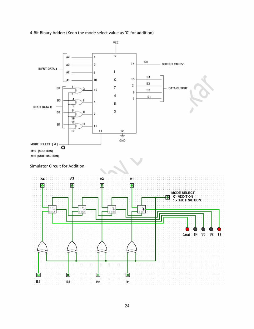
24
4-Bit Binary Adder: (Keep the mode select value as ‘0’ for addition)
Simulator Circuit for Addition:

25
4-Bit Binary Subtractor using 1’s complement:
Simulator circuit for 1’s Complement:

26
4-Bit Binary Subtractor using 2’s complement:
Simulator circuit for 2’s Complement:

27
Test Data:
INPUT DATA A INPUT DATA B ADDITION
A4 A3 A2 A1 B4 B3 B2 B1 Cout S4 S3 S2 S1
1 0 0 0 0 0 1 0 0 1 0 1 0
1 0 0 1 1 0 0 0 1 0 0 0 1
INPUT DATA A INPUT DATA B 1’S COMPLEMENT SUBTRACTION
1 0 0 0 0 0 1 0 0 0 1 1 0
1 0 0 1 1 0 0 0 0 0 0 0 1
INPUT DATA A INPUT DATA B 2’S COMPLEMENT SUBTRACTION
1 0 0 0 0 0 1 0 0 0 1 1 0
1 0 0 1 1 0 0 0 0 0 0 0 1
Result:-
The 4-Bit Binary addition and subtraction using 4-Bit Binary Adder/Subtractor is verified.

28
10. Implementation of Multiplexer.
Aim:-
To implement 4:1 Multiplexer and 8:1 Multiplexer using Logisim.
Apparatus required:-
Logisim Simulator
Procedure:-
1. Connection is given as per the diagram for 4:1 Multiplexer.
2. Vary the input select lines S0, S1 and Input Lines A to D and record the results.
3. Connection is given as per the diagram for 8:1 Multiplexer.
4. Vary the input select lines S0, S1,S2 and Input Lines A to H and record the results.
Note: Either circuit1 or circuit2 can be implemented.
Circuit:
4:1 Multiplexer:

29
Truth Table 4:1 Multiplexer:
INPUTS OUTPUT
E(Enable) S1 S0 A B C D Y
0 X X X X X X 0
1 0 0 0 X X X 0
1 0 0 1 X X X 1
1 1 0 X 0 X X 0
1 1 0 X 1 X X 1
1 0 1 X X 0 X 0
1 0 1 X X 1 X 1
1 1 1 X X X 0 0
1 1 1 X X X 1 1
8:1 Multiplexer:

30
Truth Table 8:1 Multiplexer:
INPUTS OUTPUT
E(Enable) S2 S1 S0 A B C D E F G H Y
0 X X X X X X X X X X X 0
1 0 0 0 0 X X X X X X X 0
1 0 0 0 1 X X X X X X X 1
1 0 1 0 X 0 X X X X X X 0
1 0 1 0 X 1 X X X X X X 1
1 0 0 1 X X 0 X X X X X 0
1 0 0 1 X X 1 X X X X X 1
1 0 1 1 X X X 0 X X X X 0
1 0 1 1 X X X 1 X X X X 1
1 1 0 0 0 X X X 0 X X X 0
1 1 0 0 1 X X X 1 X X X 1
1 1 1 0 X 0 X X X 0 X X 0
1 1 1 0 X 1 X X X 1 X X 1
1 1 0 1 X X 0 X X X 0 X 0
1 1 0 1 X X 1 X X X 1 X 1
1 1 1 1 X X X 0 X X X 0 0
1 1 1 1 X X X 1 X X X 1 1
Result:-
The 4:1 Multiplexer and 8:1 Multiplexer is constructed and the output is verified.

31
11. Implementation of DeMultiplexer.
Aim:-
To implement 1:4 DeMultiplexer and 1:8 DeMultiplexer using Logisim simulator.
Apparatus required:-
• Logisim simulator.
Procedure:-
1. Connection is given as per the diagram for DeMultiplexer.
2. Vary the inputs S1, S0 and D and record the results for 1:4 DeMultiplexer.
2. Vary the inputs S2,S1, S0 and D and record the results for 1:8 DeMultiplexer.
1:4 DeMultiplexer: Circuit:
Truth Table:
INPUTS OUTPUTS
E(Enable) S1 S0 D F0 F1 F2 F3
0 X X X X X X X
1 0 0 0 0 X X X
1 0 0 1 1 X X X
1 0 1 0 X 0 X X
1 0 1 1 X 1 X X
1 1 0 0 X X 0 X
1 1 0 1 X X 1 X
1 1 1 0 X X X 0
1 1 1 1 X X X 1

32
1:8 DeMultiplexer:
Circuit:
Truth Table:
INPUTS OUTPUTS
E(Enable) S2 S1 S0 D F0 F1 F2 F3 F4 F5 F6 F7
0 X X X X X X X X X X X X
1 0 0 0 0 0 X X X X X X X
1 0 0 0 1 1 X X X X X X X
1 0 0 1 0 X 0 X X X X X X
1 0 0 1 1 X 1 X X X X X X
1 0 1 0 0 X X 0 X X X X X
1 0 1 0 1 X X 1 X X X X X
1 0 1 1 0 X X X 0 X X X X
1 0 1 1 1 X X X 1 X X X X
1 1 0 0 0 X X X X 0 X X X
1 1 0 0 1 X X X X 1 X X X
1 1 0 1 0 X X X X X 0 X X
1 1 0 1 1 X X X X X 1 X X
1 1 1 0 0 X X X X X X 0 X
1 1 1 0 1 X X X X X X 1 X
1 1 1 1 0 X X X X X X X 0
1 1 1 1 1 X X X X X X X 1
Result:- The 1:4 and 1:8 DeMultiplexers are constructed and the output is verified.
33
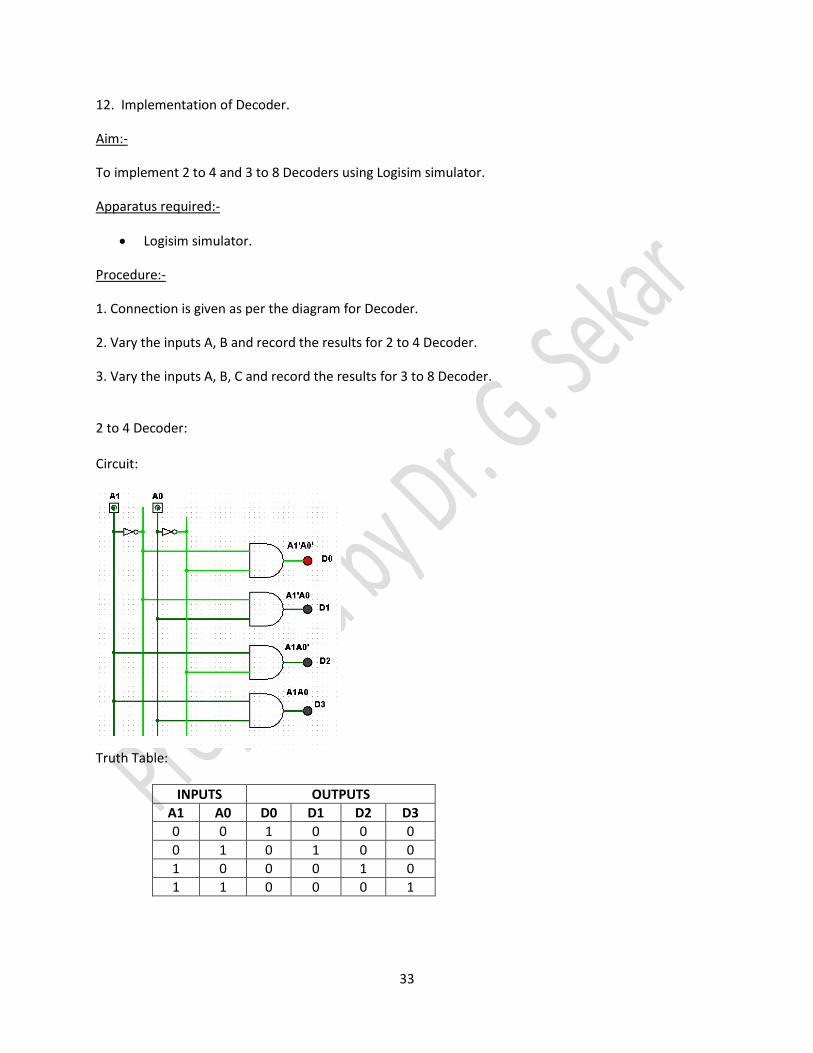
12. Implementation of Decoder.
Aim:-
To implement 2 to 4 and 3 to 8 Decoders using Logisim simulator.
Apparatus required:-
• Logisim simulator.
Procedure:-
1. Connection is given as per the diagram for Decoder.
2. Vary the inputs A, B and record the results for 2 to 4 Decoder.
3. Vary the inputs A, B, C and record the results for 3 to 8 Decoder.
2 to 4 Decoder: Circuit:
Truth Table:
INPUTS OUTPUTS
A1 A0 D0 D1 D2 D3
0 0 1 0 0 0
0 1 0 1 0 0
1 0 0 0 1 0
1 1 0 0 0 1

34
3 to 8 DECODER: Circuit:
Truth Table:
INPUT OUTPUT
A2 A1 A0 D0 D1 D2 D3 D4 D5 D6 D7
0 0 0 1 0 0 0 0 0 0 0
0 0 1 0 1 0 0 0 0 0 0
0 1 0 0 0 1 0 0 0 0 0
0 1 1 0 0 0 1 0 0 0 0
1 0 0 0 0 0 0 1 0 0 0
1 0 1 0 0 0 0 0 1 0 0
1 1 0 0 0 0 0 0 0 1 0
1 1 1 0 0 0 0 0 0 0 1
Result:-
The 2 to 4 and 3 to 8 Decoders are constructed and the output is verified.

35
13. Implementation of 4 to 2 Encoder and 8 to 3 Encoder.
Aim:-
To implement 4 to 2 Encoder and 8 to 3 Encoder using Logisim simulator.
Apparatus required:-
• Logisim simulator.
Procedure:-
1. Connection is given as per the diagram for 4 to 2 Encoder and 8 to 3 Encoder.
2. Vary the inputs D0 to D4 and record the output Q1 and Q0 for 4 to 2 Encoder.
3. Vary the inputs d0 to D7 and record the output Q2, Q1 and Q0 for 8 to 3 Encoder. 4 to 2 Encoder: Circuit:
Truth Table:
Q1 = D2 + D3 Q0 = D1 + D3
Inputs Outputs
D3 D2 D1 D0 Q1 Q0
0 0 0 1 0 0
0 0 1 0 0 1
0 1 0 0 1 0
1 0 0 0 1 1
0 0 0 0 X X

36
8 to 3 Encoder: Circuit:
Truth Table:
INPUT OUTPUT
D7 D6 D5 D4 D3 D2 D1 D0 Q2 Q1 Q0
0 0 0 0 0 0 0 1 0 0 0
0 0 0 0 0 0 1 0 0 0 1
0 0 0 0 0 1 0 0 0 1 0
0 0 0 0 1 0 0 0 0 1 1
0 0 0 1 0 0 0 0 1 0 0
0 0 1 0 0 0 0 0 1 0 1
0 1 0 0 0 0 0 0 1 1 0
1 0 0 0 0 0 0 0 1 1 1
Q2 = D4 + D5 + D6 + D7
Q1= D2 + D3 + D6 + D7
Q0= D1 + D3 + D5 + D7
Result:-
The 4 to 2 Encoder and 8 to 3 Encoder is constructed and the output is verified.

37
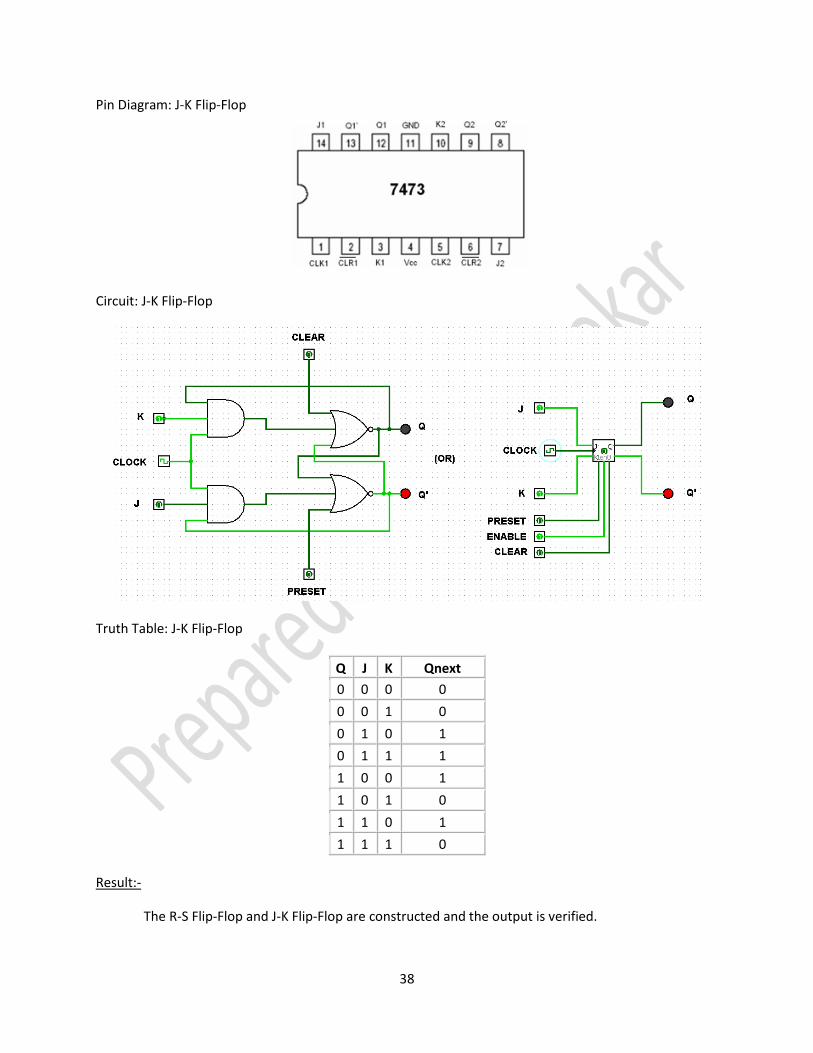
14. Implementation of R-S Flip-Flop and J-K Flip-Flop.
Aim:-
To implement R-S Flip-Flop and J-K Flip_Flop.
Apparatus required:-
• NOT - 7404
• AND - 7408
• NOR - 7402
• DUAL JK FLIP-FLOP - 7473
• IC TRAINER KIT
(or)
Logisim Simulator
Procedure:-
1. Connection is given as per the diagram for R-S Flip-Flop and J-K Flip-Flop.
2. Vary the inputs R and S for R-S Flip-Flop and J and K for J-K Flip-Flop and record the results.
Circuit: R-S Flip-Flop
Truth Table: R-S Flip-Flop
Q S R Qnext
0 0 0 0
0 0 1 0
0 1 0 1
0 1 1 Indeterminate
1 0 0 1
1 0 1 0
1 1 0 1
1 1 1 Indeterminate
38
Pin Diagram: J-K Flip-Flop
Circuit: J-K Flip-Flop
Truth Table: J-K Flip-Flop
Q J K Qnext
0 0 0 0
0 0 1 0
0 1 0 1
0 1 1 1
1 0 0 1
1 0 1 0
1 1 0 1
1 1 1 0
Result:-
The R-S Flip-Flop and J-K Flip-Flop are constructed and the output is verified.

39
15. Implementation of Shift Register-Serial Transfer.
Aim:-
To shift the given 4-Bit data using the J-K Flip-Flops.
Apparatus required:-
• J-K Flip-Flop - 7473
• IC TRAINER KIT
(or)
Logisim Simulator.
Procedure:-
To enter 4-Bit data (1010)
Initially apply clear signal as low (0) to clear the registers, so Q4Q3Q2Q1 = 0000 1. To enter bit 1:-
Hold J1 -> “1” and K1 -> “0” and give one clock pulse.
Q4Q3Q2Q1 = 0001 2. To enter bit 2:-
Hold J1 -> “0” and K1 -> “1” and give one clock pulse.
Q4Q3Q2Q1 = 0010 3. To enter bit 3:-
Hold J1 -> “1” and K1 -> “0” and give one clock pulse.
Q4Q3Q2Q1 = 0101 4. To enter bit 4:-
Hold J1 -> “0” and K1 -> “1” and give one clock pulse.
Q4Q3Q2Q1 = 1010

40
Circuit Diagram:
FF1
J1
K1
Q1
Q1
FF2
J2
K2
Q2
Q2
FF3
J3
K3
Q3
Q3
FF4
J4
K4
Q4
Q4
Q1 Q2 Q3 Q4
CLK
CLR
I
N
P
U
T
Truth Table:
INPUT CONDITION
PRESENT STATE AFTER CLOCK PULSE
Q4 Q3 Q2 Q1 Q4 Q3 Q2 Q1
J1=1 K1=0 X X X X X X X 1
J1=0 K1=1 X X X 1 X X 1 0
J1=1 K1=0 X X 1 0 X 1 0 1
J1=0 K1=1 X 1 0 1 1 0 1 0
Result:-
The given 4-Bit data is shifted and verified.

41
16. Implementation of 3bits binary Up/Down Counter.
Aim:-
To construct a 3bits binary Up/Down counter using J-K Flip-Flop.
Apparatus required:-
• J-K Flip-Flop - 7473
• IC TRAINER KIT
(or)
Logisim Simulator
Procedure:-
1. Connections are given as per the circuit diagram.
2. The CLK connections of all Flip-Flops are connected to a pulse generator.
3. The counting sequence given in the truth table is viewed in the output panel.
Circuit Diagram:

42
Truth Table:
Clock Pulse UP Q2 Q1 Q0 DOWN
0 0 0 0
1 0 0 1
2 0 1 0
3 0 1 1
4 1 0 0
5 1 0 1
6 1 1 0
7 1 1 1
Timing Diagram:
Result:-
The 3-Bit Up/Down counter has been constructed and the counting sequence is also verified.