1a, 76v, high-efficiency maxpower step-down dc … max5035 delivers up to 1a output current. ......
TRANSCRIPT

AVAILABLE
Functional Diagrams
Pin Configurations appear at end of data sheet.Functional Diagrams continued at end of data sheet.UCSP is a trademark of Maxim Integrated Products, Inc.
For pricing, delivery, and ordering information, please contact Maxim Direct at 1-888-629-4642, or visit Maxim’s website at www.maximintegrated.com.
EVALUATION KIT AVAILABLE
General DescriptionThe MAX5035 easy-to-use, high-efficiency, high-volt-age, step-down DC-DC converter operates from aninput voltage up to 76V and consumes only 270µA qui-escent current at no load. This pulse-width modulated(PWM) converter operates at a fixed 125kHz switchingfrequency at heavy loads, and automatically switchesto pulse-skipping mode to provide low quiescent cur-rent and high efficiency at light loads. The MAX5035includes internal frequency compensation simplifyingcircuit implementation. The device uses an internal low-on-resistance, high-voltage, DMOS transistor to obtainhigh efficiency and reduce overall system cost. Thisdevice includes undervoltage lockout, cycle-by-cyclecurrent limit, hiccup mode output short-circuit protec-tion, and thermal shutdown.
The MAX5035 delivers up to 1A output current. The out-put current may be limited by the maximum power dis-sipation capability of the package. External shutdown isincluded, featuring 10µA (typ) shutdown current. TheMAX5035A/B/C versions have fixed output voltages of3.3V, 5V, and 12V, respectively, while the MAX5035D/Eversions have an adjustable output voltage from 1.25Vto 13.2V.
The MAX5035 is available in space-saving 8-pin SOand 8-pin plastic DIP packages and operates over theautomotive (-40°C to +125°C) temperature range.
ApplicationsAutomotive
Consumer Electronics
Industrial
Distributed Power
Features Wide 7.5V to 76V Input Voltage Range
Fixed (3.3V, 5V, 12V) and Adjustable (1.25V to 13.2V) Versions
1A Output Current
Efficiency Up to 94%
Internal 0.4Ω High-Side DMOS FET
270µA Quiescent Current at No Load, 10µAShutdown Current
Internal Frequency Compensation
Fixed 125kHz Switching Frequency
Thermal Shutdown and Short-Circuit CurrentLimit
8-Pin SO and PDIP Packages
1A, 76V, High-Efficiency MAXPower Step-Down DC-DC Converter
Ordering Information
19-2988; Rev 5; 5/11
PART TEMP RANGEPIN-PACKAGE
OU TPU TVO LTA GE
( V)
MAX5035AUSA 0°C to +85°C 8 SO
MAX5035AUPA 0°C to +85°C 8 PDIP
MAX5035AASA -40°C to +125°C 8 SO
M AX 5035AAS A/V + -40°C to +125°C 8 SO
3.3
MAX5035BUSA 0°C to +85°C 8 SO
MAX5035BUPA 0°C to +85°C 8 PDIP
MAX5035BASA -40°C to +125°C 8 SO
M AX 5035BAS A/V + -40°C to +125°C 8 SO
5.0
1
2
3
4
BST
VD
SGND
FB
8
7
6
5
LX
TOP VIEW
VIN
GND
ON/OFF
MAX5035
SO/PDIP
Pin Configuration
MAX5035
GND
BST
LX
VIN
SGND
FB
D150SQ100
VD
100µH VOUT5V
VIN7.5V TO 76V
68µF
0.1µF
0.1µF
68µFON
OFF
R1
R2
ON/OFF
Typical Operating Circuit
/V denotes an automotive qualified part.+Denotes a lead(Pb)-free/RoHS-compliant package.Ordering Information continued at end of data sheet.
MAX5035
Ordering Information

1A, 76V, High-Efficiency MAXPower Step-Down DC-DC ConverterABSOLUTE MAXIMUM RATINGS
Stresses beyond those listed under “Absolute Maximum Ratings” may cause permanent damage to the device. These are stress ratings only, and functionaloperation of the device at these or any other conditions beyond those indicated in the operational sections of the specifications is not implied. Exposure toabsolute maximum rating conditions for extended periods may affect device reliability.
(Voltages referenced to GND, unless otherwise specified.)VIN .........................................................................-0.3V to +80VSGND ....................................................................-0.3V to +0.3VLX.................................................................-0.8V to (VIN + 0.3V)BST ...............................................................-0.3V to (VIN + 10V)BST (transient < 100ns) ................................-0.3V to (VIN + 15V)BST to LX................................................................-0.3V to +10VBST to LX (transient < 100ns) ................................-0.3V to +15VON/OFF ..................................................................-0.3V to +80VVD...........................................................................-0.3V to +12VFB
MAX5035A/MAX5035B/MAX5035C ...................-0.3V to +15VMAX5035D/E ......................................................-0.3V to +12V
VOUT Short-Circuit Duration (VIN ≤ 40V)........................Indefinite
VD Short-Circuit Duration ..............................................IndefiniteContinuous Power Dissipation (TA = +70°C)
8-Pin PDIP (derate 9.1mW/°C above +70°C)...............727mW8-Pin SO (derate 5.9mW/°C above +70°C)..................471mW
Operating Temperature RangeMAX5035_U_ _ ...................................................0°C to +85°CMAX5035_A_ _ ..............................................-40°C to +125°C
Storage Temperature Range .............................-65°C to +150°CJunction Temperature ......................................................+150°CLead Temperature (soldering, 10s) .................................+300°CSoldering Temperature (reflow)
Lead(Pb)-free...............................................................+260°CContaining lead(Pb) .....................................................+240°C
ELECTRICAL CHARACTERISTICS (MAX5035_U_ _)(VIN = +12V, VON/OFF = +12V, IOUT = 0, TA = 0°C to +85°C, unless otherwise noted. Typical values are at TA = +25°C. See theTypical Application Circuit.)
PARAMETER SYMBOL CONDITIONS MIN TYP MAX UNITS
MAX5035A 7.5 76.0
MAX5035B 7.5 76.0
MAX5035C 15 76Input Voltage Range VIN
MAX5035D/E 7.5 76.0
V
Undervoltage Lockout UVLO 5.2 V
MAX5035AVIN = 7.5V to 76V,IOUT = 20mA to 1A
3.185 3.3 3.415
MAX5035BVIN = 7.5V to 76V,IOUT = 20mA to 1A
4.85 5.0 5.15Output Voltage VOUT
MAX5035CVIN = 15V to 76V,IOUT = 20mA to 1A
11.64 12 12.36
V
VIN = 7.5V to 76V, MAX5035D/E 1.192 1.221 1.250Feedback Voltage VFB
VIN = 7.5V to 76V, MAX5035E 1.185 1.221 1.250V
VIN = 12V, ILOAD = 0.5A, MAX5035A 86
VIN = 12V, ILOAD = 0.5A, MAX5035B 90
VIN = 24V, ILOAD = 0.5A, MAX5035C 94Efficiency η
VIN = 12V, VOUT = 5V, ILOAD = 0.5A,MAX5035D/E
90
%
VFB = 3.5V, VIN = 7.5V to 76V, MAX5035A 270 440
VFB = 5.5V, VIN = 7.5V to 76V, MAX5035B 270 440
VFB = 13V, VIN = 15V to 76V, MAX5035C 270 440
VFB = 1.3V, MAX5035D 270 440
Quiescent Supply Current IQ
VFB = 1.3V, MAX5035E 340 460
µA
Shutdown Current ISHDN VON/OFF = 0V, VIN = 7.5V to 76V 10 45 µA
Peak Switch Current Limit ILIM (Note 1) 1.30 1.9 2.50 A
MAX5035
2 Maxim Integrated

1A, 76V, High-Efficiency MAXPower Step-Down DC-DC Converter
ELECTRICAL CHARACTERISTICS (continued) (MAX5035_U_ _)(VIN = +12V, VON/OFF = +12V, IOUT = 0, TA = 0°C to +85°C, unless otherwise noted. Typical values are at TA = +25°C. See theTypical Application Circuit.)
PARAMETER SYMBOL CONDITIONS MIN TYP MAX UNITS
Switch Leakage Current IOL VIN = 76V, VON/OFF = 0V, VLX = 0V 0.01 1 µA
Switch On-Resistance RDS(ON) ISWITCH = 1A 0.40 0.80 ΩPFM Threshold IPFM Minimum switch current in any cycle 55 85 130 mA
FB Input Bias Current IB MAX5035D/E -150 +0.01 +150 nA
ON/OFF CONTROL INPUT
Rising trip point for MAX5035A/B/C/D 1.53 1.69 1.85ON/OFF Input-Voltage Threshold VON/OFF
Rising trip point for MAX5035E 1.40 1.65 1.90V
ON/OFF Input-Voltage Hysteresis VHYST 100 mV
ON/OFF Input Current ION/OFF VON/OFF = 0V to VIN 10 150 nA
ON/OFF Operating VoltageRange
VON/OFF 76 V
OSCILLATOR
Oscillator Frequency fOSC 109 125 135 kHz
Maximum Duty Cycle DMAX MAX5035D/E 95 %
VOLTAGE REGULATOR
Regulator Output Voltage VD VIN = 8.5V to 76V, IL = 0 6.9 7.8 8.8 V
Dropout Voltage 7.5V ≤ VIN ≤ 8.5V, IL = 1mA 2.0 V
Load Regulation ∆VD/∆IVD 0 to 5mA 150 ΩPACKAGE THERMAL CHARACTERISTICS
SO package (JEDEC 51) 170Thermal Resistance(Junction to Ambient)
θJADIP package (JEDEC 51) 110
°C/W
THERMAL SHUTDOWN
Thermal-Shutdown JunctionTemperature
TSH +160 °C
Thermal-Shutdown Hysteresis THYST 20 °C
ELECTRICAL CHARACTERISTICS (MAX5035_A_ _)(VIN = +12V, VON/OFF = +12V, IOUT = 0, TA = TJ = -40°C to +125°C, unless otherwise noted. Typical values are at TA = +25°C. Seethe Typical Application Circuit.) (Note 2)
PARAMETER SYMBOL CONDITIONS MIN TYP MAX UNITS
MAX5035A 7.5 76.0
MAX5035B 7.5 76.0
MAX5035C 15 76Input Voltage Range VIN
MAX5035D/E 7.5 76.0
V
Undervoltage Lockout UVLO 5.2 V
MAX5035AVIN = 7.5V to 76V,IOUT = 20mA to 1A
3.185 3.3 3.415
MAX5035BVIN = 7.5V to 76V,IOUT = 20mA to 1A
4.825 5.0 5.175Output Voltage VOUT
MAX5035CVIN = 15V to 76V,IOUT = 20mA to 1A
11.58 12 12.42
V
MAX5035
Maxim Integrated 3

1A, 76V, High-Efficiency MAXPower Step-Down DC-DC ConverterELECTRICAL CHARACTERISTICS (MAX5035_A_ _) (continued)(VIN = +12V, VON/OFF = +12V, IOUT = 0, TA = TJ = -40°C to +125°C, unless otherwise noted. Typical values are at TA = +25°C. Seethe Typical Application Circuit.) (Note 2)
PARAMETER SYMBOL CONDITIONS MIN TYP MAX UNITS
VIN = 7.5V to 76V, MAX5035D 1.192 1.221 1.250Feedback Voltage VFB
VIN = 7.5V to 76V, MAX5035E 1.185 1.221 1.250V
VIN = 12V, ILOAD = 0.5A, MAX5035A 86
VIN = 12V, ILOAD = 0.5A, MAX5035B 90
VIN = 24V, ILOAD = 0.5A, MAX5035C 94Efficiency η
VIN = 12V, VOUT = 5V, ILOAD = 0.5A,MAX5035D/E
90
%
VFB = 3.5V, VIN = 7.5V to 76V, MAX5035A 270 440
VFB = 5.5V, VIN = 7.5V to 76V, MAX5035B 270 440
VFB = 13V, VIN = 15V to 76V, MAX5035C 270 440
VFB = 1.3V, MAX5035D 270 440
Quiescent Supply Current IQ
VFB = 1.3V, MAX5035E 340 460
µA
Shutdown Current ISHDN VON/OFF = 0V, VIN = 7.5V to 76V 10 45 µA
Peak Switch Current Limit ILIM (Note 1) 1.30 1.9 2.50 A
VIN = 76V, VON/OFF = 0V, VLX = 0V 1
Switch Leakage Current IOL VIN = 76V, VON/OFF = 0V, VLX = 0V,MAX5035E
5µA
Switch On-Resistance RDS(ON) ISWITCH = 1A 0.40 0.80 ΩPFM Threshold IPFM Minimum switch current in any cycle 55 85 130 mA
FB Input Bias Current IB MAX5035D/E -150 +0.01 +150 nA
ON/OFF CONTROL INPUT
Rising trip point for MAX5035A/B/C/D 1.50 1.69 1.85ON/OFF Input-Voltage Threshold VON/OFF
Rising trip point for MAX5035E 1.40 1.65 1.90V
ON/OFF Input-Voltage Hysteresis VHYST 100 mV
ON/OFF Input Current ION/OFF VON/OFF = 0V to VIN 10 150 nA
ON/OFF Operating VoltageRange
VON/OFF 76 V
OSCILLATOR
Oscillator Frequency fOSC 105 125 137 kHz
Maximum Duty Cycle DMAX MAX5035D/E 95 %
VOLTAGE REGULATOR
Regulator Output Voltage VD VIN = 8.5V to 76V, IL = 0 6.5 7.8 9.0 V
Dropout Voltage 7.5V ≤ VIN ≤ 8.5V, IL = 1mA 2.0 V
Load Regulation ∆VD/∆IVD 0 to 5mA 150 Ω
MAX5035
4 Maxim Integrated

1A, 76V, High-Efficiency MAXPower Step-Down DC-DC Converter
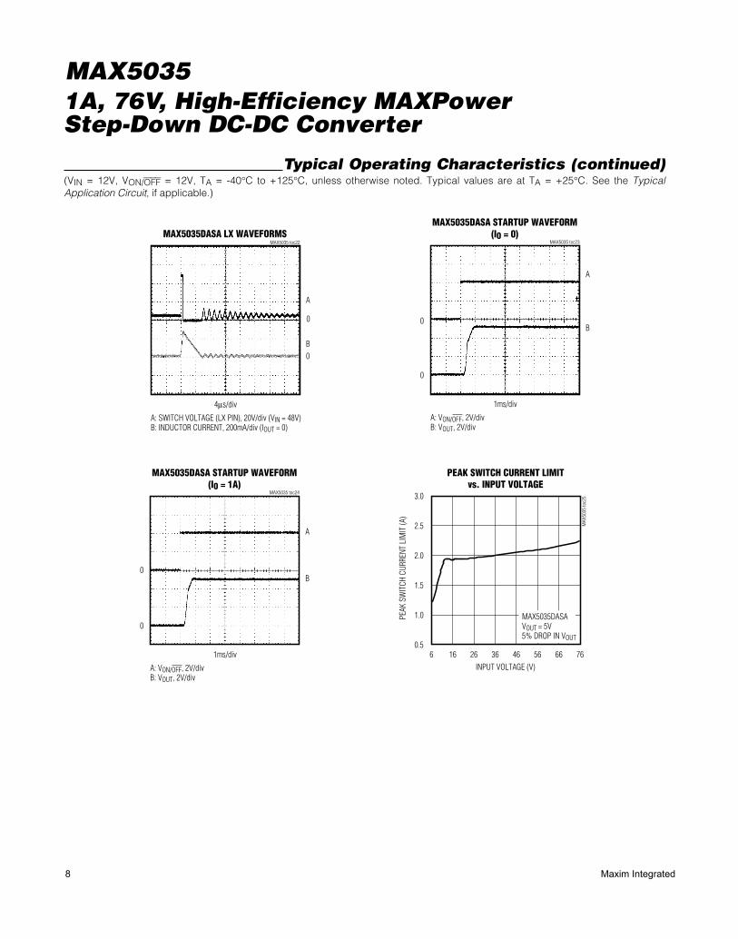
Typical Operating Characteristics(VIN = 12V, VON/OFF = 12V, TA = -40°C to +125°C, unless otherwise noted. Typical values are at TA = +25°C. See the TypicalApplication Circuit, if applicable.)
PARAMETER SYMBOL CONDITIONS MIN TYP MAX UNITS
PACKAGE THERMAL CHARACTERISTICS
SO package (JEDEC 51) 170Thermal Resistance(Junction to Ambient)
θJADIP package (JEDEC 51) 110
°C/W
THERMAL SHUTDOWN
Thermal-Shutdown JunctionTemperature
TSH +160 °C
Thermal-Shutdown Hysteresis THYST 20 °C
Note 1: Switch current at which current limit is activated.Note 2: All limits at -40°C are guaranteed by design, not production tested.
VOUT vs. TEMPERATURE(MAX5035AASA, VOUT = 3.3V)
MAX
5035
toc0
1
TEMPERATURE (°C)
V OUT
(V)
3.24
3.28
3.32
3.36
3.40
3.20
IOUT = 0.1A
IOUT = 1A
100500-50 150-25 25 75 125
VOUT vs. TEMPERATURE(MAX5035DASA, VOUT = 5V)
MAX
5035
toc0
2
TEMPERATURE (°C)
V OUT
(V)
125100-25 0 25 50 75
4.85
4.90
4.95
5.00
5.05
5.10
5.15
5.20
4.80-50 150
IOUT = 0.1A
IOUT = 1A
LINE REGULATION(MAX5035AASA, VOUT = 3.3V)
MAX
5035
toc0
3
INPUT VOLTAGE (V)
OUTP
UT V
OLTA
GE (V
)
65503520
3.24
3.28
3.32
3.36
3.40
3.205 80
IOUT = 1A
IOUT = 0.1A
LINE REGULATION(MAX5035DASA, VOUT = 5V)
MAX
5035
toc0
4
INPUT VOLTAGE (V)
OUTP
UT V
OLTA
GE (V
)
655020 35
4.85
4.90
4.95
5.00
5.05
5.10
5.15
5.20
4.805 80
IOUT = 1A
IOUT = 0.1A
LOAD REGULATION(MAX5035AASA, VOUT = 3.3V)
MAX
5035
toc0
5
ILOAD (mA)
V OUT
(V)
800600400200
3.24
3.28
3.32
3.36
3.40
3.200 1000
VIN = 7.5V, 24V
VIN = 76V
LOAD REGULATION(MAX5035DASA, VOUT = 5V)
MAX
5035
toc0
6
ILOAD (mA)
V OUT
(V)
800600400200
4.95
5.00
5.05
5.10
4.900 1000
VIN = 76V
VIN = 24V
VIN = 7.5V
ELECTRICAL CHARACTERISTICS (MAX5035_A_ _) (continued)(VIN = +12V, VON/OFF = +12V, IOUT = 0, TA = TJ = -40°C to +125°C, unless otherwise noted. Typical values are at TA = +25°C. Seethe Typical Application Circuit.) (Note 2)
MAX5035
Maxim Integrated 5

1A, 76V, High-Efficiency MAXPower Step-Down DC-DC Converter
Typical Operating Characteristics (continued)(VIN = 12V, VON/OFF = 12V, TA = -40°C to +125°C, unless otherwise noted. Typical values are at TA = +25°C. See the TypicalApplication Circuit, if applicable.)
OUTPUT CURRENT LIMIT vs. TEMPERATURE
MAX
5035
toc1
0
TEMPERATURE (°C)
OUTP
UT C
URRE
NT L
IMIT
(A)
1251007550250-25
0.5
1.0
1.5
2.0
0-50 150
MAX5035DASAVOUT = 5V5% DROP IN VOUT
OUTPUT CURRENT LIMITvs. INPUT VOLTAGE
MAX
5035
toc1
1
INPUT VOLTAGE (V)
OUTP
UT C
URRE
NT L
IMIT
(A)
65503520
0.8
1.1
1.4
1.7
2.0
0.55 80
MAX5035DASAVOUT = 5V
5% DROP IN VOUT
QUIESCENT SUPPLY CURRENTvs. TEMPERATURE
MAX
5035
toc1
2
TEMPERATURE (°C)
QUIE
SCEN
T SU
PPLY
CUR
RENT
(µA)
230
260
290
320
350
200100500-50 150-25 25 75 125
QUIESCENT SUPPLY CURRENTvs. INPUT VOLTAGE
MAX
5035
toc1
3
INPUT VOLTAGE (V)
QUIE
SCEN
T SU
PPLY
CUR
RENT
(µA)
665646362616
230
260
290
320
350
2006 76
SHUTDOWN CURRENTvs. TEMPERATURE
MAX
5035
toc1
4
TEMPERATURE (°C)
SHUT
DOW
N CU
RREN
T (µ
A)
5
10
15
20
25
0100500-50 150-25 25 75 125
SHUTDOWN CURRENT vs. INPUT VOLTAGEM
AX50
35 to
c15
INPUT VOLTAGE (V)
SHUT
DOW
N CU
RREN
T (µ
A)
665646362616
4
8
12
16
20
06 76
EFFICIENCY vs. LOAD CURRENT(MAX5035AASA, VOUT = 3.3V)
MAX
5035
toc0
7
LOAD CURRENT (mA)
EFFI
CIEN
CY (%
)
800600400200
10
20
30
40
50
60
70
80
90
100
00 1000
VIN = 76V
VIN = 48V
VIN = 24V
VIN = 12V
VIN = 7.5V
EFFICIENCY vs. LOAD CURRENT(MAX5035DASA, VOUT = 5V)
MAX
5035
toc0
8
LOAD CURRENT (mA)
EFFI
CIEN
CY (%
)
800600400200
10
20
30
40
50
60
70
80
90
100
00 1000
VIN = 76V
VIN = 48V
VIN = 24V
VIN = 12V
VIN = 7.5V
EFFICIENCY vs. LOAD CURRENT(MAX5035DASA, VOUT = 12V)
MAX
5035
toc0
9
LOAD CURRENT (mA)
EFFI
CIEN
CY (%
)
800600400200
10
20
30
40
50
60
70
80
90
100
00 1000
VIN = 76V
VIN = 48V
VIN = 24V
VIN = 15V
MAX5035
6 Maxim Integrated

1A, 76V, High-Efficiency MAXPower Step-Down DC-DC Converter
Typical Operating Characteristics (continued)(VIN = 12V, VON/OFF = 12V, TA = -40°C to +125°C, unless otherwise noted. Typical values are at TA = +25°C. See the TypicalApplication Circuit, if applicable.)
OUTPUT VOLTAGEvs. INPUT VOLTAGE
MAX
5035
toc1
6
VIN (V)
V OUT
(V)
12963
3
6
9
12
15
00 15
IOUT = 0
IOUT = 0.3A
IOUT = 1A
MAX5035DASAVOUT = 12VVON/OFF = VIN
MAX5035DASA LOAD-TRANSIENT RESPONSE
MAX5035 toc17
400µs/div
B
A
A: VOUT, 200mV/div, AC-COUPLEDB: IOUT, 500mA/div, 0.1A TO 1A
VOUT = 5V
MAX5035DASALOAD-TRANSIENT RESPONSE
MAX5035 toc18
400µs/div
B
A
A: VOUT, 200mV/div, AC-COUPLEDB: IOUT, 500mA/div, 0.5A TO 1A
VOUT = 5V
MAX5035DASALOAD-TRANSIENT RESPONSE
MAX5035 toc19
400µs/div
B
A
A: VOUT, 200mV/div, AC-COUPLEDB: IOUT, 500mA/div, 0.1A TO 0.5A
VOUT = 5V
MAX5035DASA LX WAVEFORMSMAX5035 toc20
4µs/div
B
0
A
0
A: SWITCH VOLTAGE (LX PIN), 20V/div (VIN = 48V)B: INDUCTOR CURRENT, 500mA/div (IOUT = 1A)
MAX5035DASA LX WAVEFORMSMAX5035 toc21
4µs/div
B
0
A
0
A: SWITCH VOLTAGE (LX PIN), 20V/div (VIN = 48V)B: INDUCTOR CURRENT, 200mA/div (IOUT = 100mA)
MAX5035
Maxim Integrated 7
1A, 76V, High-Efficiency MAXPower Step-Down DC-DC Converter
Typical Operating Characteristics (continued)(VIN = 12V, VON/OFF = 12V, TA = -40°C to +125°C, unless otherwise noted. Typical values are at TA = +25°C. See the TypicalApplication Circuit, if applicable.)
MAX5035DASA LX WAVEFORMSMAX5035 toc22
4µs/div
B
A
A: SWITCH VOLTAGE (LX PIN), 20V/div (VIN = 48V)B: INDUCTOR CURRENT, 200mA/div (IOUT = 0)
0
0
MAX5035DASA STARTUP WAVEFORM(IO = 0)
MAX5035 toc23
1ms/div
B
A
A: VON/OFF, 2V/divB: VOUT, 2V/div
0
0
MAX5035DASA STARTUP WAVEFORM(IO = 1A)
MAX5035 toc24
1ms/div
B
A
A: VON/OFF, 2V/divB: VOUT, 2V/div
0
0
PEAK SWITCH CURRENT LIMITvs. INPUT VOLTAGE
MAX
5035
toc2
5
INPUT VOLTAGE (V)
PEAK
SW
ITCH
CUR
RENT
LIM
IT (A
)
56 6646362616
1.0
1.5
2.0
2.5
3.0
0.56 76
MAX5035DASAVOUT = 5V5% DROP IN VOUT
MAX5035
8 Maxim Integrated

1A, 76V, High-Efficiency MAXPower Step-Down DC-DC Converter
Pin Description
PIN NAME FUNCTION
1 BST Boost Capacitor Connection. Connect a 0.1µF ceramic capacitor from BST to LX.
2 VD Internal Regulator Output. Bypass VD to GND with a 0.1µF ceramic capacitor.
3 SGND Internal Connection. SGND must be connected to GND.
4 FBOutput Sense Feedback Connection. For fixed output voltage (MAX5035A, MAX5035B, MAX5035C),connect FB to VOUT. For adjustable output voltage (MAX5035D, MAX5035E), use an external resistivevoltage-divider to set VOUT. VFB regulating set point is 1.22V.
5 ON/OFFShutdown Control Input. Pull ON/OFF low to put the device in shutdown mode. Drive ON/OFF high fornormal operation.
6 GND Ground
7 VIN Input Voltage. Bypass VIN to GND with a low ESR capacitor as close to the device as possible.
8 LX Source Connection of Internal High-Side Switch
ENABLE
LX
BST
VINON/OFF
VREFREGULATOR
(FOR DRIVER)
REGULATOR(FOR ANALOG)
OSC
RAMP
HIGH-SIDECURRENT
SENSE
IREF-PFM
IREF-LIM
CPFM1.69V
CILIM
FB
x1
VREF EAMP
CONTROL LOGIC
CPWM
VD
GND
Rh
Rl
CLK
SGND
MAX5035
TYPE 3 COMPENSATION THERMAL
SHUTDOWN
RAMP
Block Diagram
MAX5035
Maxim Integrated 9

1A, 76V, High-Efficiency MAXPower Step-Down DC-DC Converter
Detailed DescriptionThe MAX5035 step-down DC-DC converter operatesfrom a 7.5V to 76V input voltage range. A unique volt-age-mode control scheme with voltage feed-forwardand an internal switching DMOS FET provides high effi-ciency over a wide input voltage range. This pulse-width modulated converter operates at a fixed 125kHzswitching frequency. The device also features automat-ic pulse-skipping mode to provide low quiescent cur-rent and high efficiency at light loads. Under no load,the MAX5035 consumes only 270µA, and in shutdownmode, consumes only 10µA. The MAX5035 also fea-tures undervoltage lockout, hiccup mode output short-circuit protection, and thermal shutdown.
Shutdown ModeDrive ON/OFF to ground to shut down the MAX5035.Shutdown forces the internal power MOSFET off, turnsoff all internal circuitry, and reduces the VIN supply cur-rent to 10µA (typ). The ON/OFF rising threshold is1.69V (typ). Before any operation begins, the voltage atON/OFF must exceed 1.69V (typ). The ON/OFF inputhas 100mV hysteresis.
Undervoltage Lockout (UVLO)Use the ON/OFF function to program the UVLO thresh-old at the input. Connect a resistive voltage-dividerfrom VIN to GND with the center node to ON/OFF asshown in Figure 1. Calculate the threshold value byusing the following formula:
The minimum recommended VUVLO(TH) is 6.5V, 7.5V, and13V for the output voltages of 3.3V, 5V, and 12V, respec-tively. The recommended value for R2 is less than 1MΩ.
If the external UVLO threshold-setting divider is notused, an internal undervoltage-lockout feature monitorsthe supply voltage at VIN and allows operation to startwhen VIN rises above 5.2V (typ). This feature can beused only when VIN rise time is faster than 2ms. Forslower VIN rise time, use the resistive-divider atON/OFF.
Boost High-Side Gate Drive (BST)Connect a flying bootstrap capacitor between LX andBST to provide the gate-drive voltage to the high-sideN-channel DMOS switch. The capacitor is alternatelycharged from the internally regulated output voltage VDand placed across the high-side DMOS driver. Use a0.1µF, 16V ceramic capacitor located as close to thedevice as possible.
On startup, an internal low-side switch connects LX toground and charges the BST capacitor to VD. Once theBST capacitor is charged, the internal low-side switchis turned off and the BST capacitor voltage providesthe necessary enhancement voltage to turn on thehigh-side switch.
Thermal-Overload ProtectionThe MAX5035 features integrated thermal overload pro-tection. Thermal overload protection limits total powerdissipation in the device, and protects the device in theevent of a fault condition. When the die temperatureexceeds +160°C, an internal thermal sensor signals theshutdown logic, turning off the internal power MOSFETand allowing the IC to cool. The thermal sensor turns theinternal power MOSFET back on after the IC’s die tem-perature cools down to +140°C, resulting in a pulsedoutput under continuous thermal overload conditions.
Applications InformationSetting the Output Voltage
The MAX5035A/B/C have preset output voltages of 3.3V,5.0V, and 12V, respectively. Connect FB to the presetoutput voltage (see the Typical Operating Circuit).The MAX5035D/E versions offer an adjustable outputvoltage. Set the output voltage with a resistive voltage-divider connected from the circuit’s output to ground(Figure 1). Connect the center node of the divider toFB. Choose R4 less than 15kΩ, then calculate R3 asfollows:
RV
ROUT31 22
1 224=
−×
( . ).
VRR
VUVLO TH( ) .= +⎛⎝⎜
⎞⎠⎟
×112
1 85
MAX5035D
GND
BST
LXVIN
SGND
FB
D150SQ100
VD
100µHVOUT5V
VIN7.5V TO 76V
68µF
0.1µF
0.1µF
COUT68µF
R1
R2 R341.2kΩ
R413.3kΩ
ON/OFF
Figure 1. Adjustable Output Voltage
MAX5035
10 Maxim Integrated

1A, 76V, High-Efficiency MAXPower Step-Down DC-DC Converter
The MAX5035 features internal compensation for opti-mum closed-loop bandwidth and phase margin. Withthe preset compensation, it is strongly advised to sensethe output immediately after the primary LC.
Inductor SelectionThe choice of an inductor is guided by the voltage dif-ference between VIN and VOUT, the required outputcurrent, and the operating frequency of the circuit. Usean inductor with a minimum value given by:
where:
IOUTMAX is the maximum output current required, andfSW is the operating frequency of 125kHz. Use an induc-tor with a maximum saturation current rating equal to atleast the peak switch current limit (ILIM). Use inductorswith low DC resistance for higher efficiency.
Selecting a RectifierThe MAX5035 requires an external Schottky rectifier asa freewheeling diode. Connect this rectifier close to thedevice using short leads and short PC board traces.Choose a rectifier with a continuous current ratinggreater than the highest expected output current. Use arectifier with a voltage rating greater than the maximumexpected input voltage, VIN. Use a low forward-voltageSchottky rectifier for proper operation and high efficien-cy. Avoid higher than necessary reverse-voltageSchottky rectifiers that have higher forward-voltagedrops. Use a Schottky rectifier with forward-voltage
drop (VFB) less than 0.45V at +25°C and maximum loadcurrent to avoid forward biasing of the internal bodydiode (LX to ground). Internal body diode conductionmay cause excessive junction temperature rise andthermal shutdown. Use Table 1 to choose the properrectifier at different input voltages and output current.
Input Bypass CapacitorThe discontinuous input-current waveform of the buckconverter causes large ripple currents in the inputcapacitor. The switching frequency, peak inductor cur-rent, and the allowable peak-to-peak voltage ripple thatreflects back to the source dictate the capacitancerequirement. The MAX5035 high switching frequencyallows the use of smaller-value input capacitors.
The input ripple is comprised of ∆VQ (caused by thecapacitor discharge) and ∆VESR (caused by the ESR ofthe capacitor). Use low-ESR aluminum electrolyticcapacitors with high ripple-current capability at the input.Assuming that the contribution from the ESR and capaci-tor discharge is equal to 90% and 10%, respectively, cal-culate the input capacitance and the ESR required for aspecified ripple using the following equations:
IOUT is the maximum output current of the converterand fSW is the oscillator switching frequency (125kHz).For example, at VIN = 48V, VOUT = 3.3V, the ESR andinput capacitance are calculated for the input peak-to-peak ripple of 100mV or less yielding an ESR andcapacitance value of 80mΩ and 51µF, respectively.
Low-ESR, ceramic, multilayer chip capacitors are recom-mended for size-optimized application. For ceramiccapacitors, assume the contribution from ESR and capaci-tor discharge is equal to 10% and 90%, respectively.
The input capacitor must handle the RMS ripple currentwithout significant rise in temperature. The maximumcapacitor RMS current occurs at about 50% duty cycle.
ESRV
IIIN
ESR
OUT
=+
∆∆ LL
INOUTC
I2
⎛⎝⎜
⎞⎠⎟
=× DD D
V f
whereQ SW
( )
:
1−×∆
( ),∆I
V V VV f LL
IN OUT OUT
IN SW=
− ×× ×
DVVOUT
IN=
DVVOUT
IN=
LV V D
I fIN OUT
OUTMAX SW=
− ×× ×
( ).0 3
VIN (V) DIODE PART NUMBER MANUFACTURER
15MQ040N IR
B240A Diodes, Inc.
B240 Central Semiconductor7.5 to 36
MBRS240, MBRS1540 ON Semiconductor
30BQ060 IR
B360A Diodes, Inc.
CMSH3-60 Central Semiconductor7.5 to 56
MBRD360, MBR3060 ON Semiconductor
50SQ100, 50SQ80 IR7.5 to 76
MBRM5100 Diodes, Inc.
Table 1. Diode Selection
MAX5035
Maxim Integrated 11

1A, 76V, High-Efficiency MAXPower Step-Down DC-DC ConverterEnsure that the ripple specification of the input capaci-tor exceeds the worst-case capacitor RMS ripple cur-rent. Use the following equations to calculate the inputcapacitor RMS current:
IPRMS is the input switch RMS current, IAVGIN is theinput average current, and η is the converter efficiency.
The ESR of aluminum electrolytic capacitors increasessignificantly at cold temperatures. Use a 1µF or greatervalue ceramic capacitor in parallel with the aluminumelectrolytic input capacitor, especially for input voltagesbelow 8V.
Output Filter CapacitorThe worst-case peak-to-peak and RMS capacitor ripplecurrent, allowable peak-to-peak output ripple voltage,and the maximum deviation of the output voltage dur-ing load steps determine the capacitance and the ESRrequirements for the output capacitors.
The output capacitance and its ESR form a zero, whichimproves the closed-loop stability of the buck regulator.Choose the output capacitor so the ESR zero frequency(fZ) occurs between 20kHz to 40kHz. Use the followingequation to verify the value of fZ. Capacitors with 100mΩto 250mΩ ESR are recommended to ensure the closed-loop stability, while keeping the output ripple low.
The output ripple is comprised of ∆VOQ (caused by thecapacitor discharge) and ∆VOESR (caused by the ESRof the capacitor). Use low-ESR tantalum or aluminumelectrolytic capacitors at the output. Assuming that thecontributions from the ESR and capacitor dischargeequal 80% and 20% respectively, calculate the output
capacitance and the ESR required for a specified rip-ple using the following equations:
The MAX5035 has an internal soft-start time (tSS) of400µs. It is important to keep the output rise time atstartup below tSS to avoid output overshoot. The outputrise time is directly proportional to the output capacitor.Use 68µF or lower capacitance at the output to controlthe overshoot below 5%.
In a dynamic load application, the allowable deviationof the output voltage during the fast-transient load dic-tates the output capacitance value and the ESR. Theoutput capacitors supply the step load current until thecontroller responds with a greater duty cycle. Theresponse time (tRESPONSE) depends on the closed-loop bandwidth of the converter. The resistive dropacross the capacitor ESR and capacitor dischargecause a voltage droop during a step load. Use a com-bination of low-ESR tantalum and ceramic capacitorsfor better transient load and ripple/noise performance.Keep the maximum output-voltage deviation above thetolerable limits of the electronics being powered.Assuming a 50% contribution each from the outputcapacitance discharge and the ESR drop, use the fol-lowing equations to calculate the required ESR andcapacitance value:
where ISTEP is the load step and tRESPONSE is theresponse time of the controller. Controller responsetime is approximately one-third of the reciprocal of theclosed-loop unity-gain bandwidth, 20kHz typically.
PCB Layout ConsiderationsProper PCB layout is essential. Minimize ground noiseby connecting the anode of the Schottky rectifier, theinput bypass capacitor ground lead, and the output fil-ter capacitor ground lead to a single point (“star”
CI t
VOUTSTEP RESPONSE
OQ=
×∆
ESRVIOUT
OESR
STEP=
∆
CI
V fOUTL
OQ SW≈
× ×∆
∆2 2.
ESRV
IOUTOESR
L=
∆∆
fC ESRZ
OUT OUT=
× × ×1
2 π
I I I I ID
IV
PRMS PK DC PK DC
AVGIN
= + + ×( )( ) ×
=
2 23
OOUT OUT
IN
PK OUTL
DC OUTL
IV
I II
I II
××
= + = −
η∆ ∆2 2
,
andDVVOUT
IN=
I I ICRMS PRMS AVGIN= −2 22
where :
MAX5035
12 Maxim Integrated

1A, 76V, High-Efficiency MAXPower Step-Down DC-DC Converter
ground configuration). A ground plane is required.Minimize lead lengths to reduce stray capacitance,trace resistance, and radiated noise. In particular,place the Schottky rectifier diode right next to the
device. Also, place BST and VD bypass capacitorsvery close to the device. Use the PC board copperplane connecting to VIN and LX for heatsinking.
MAX5035
GND
BST
LX
VIN
SGND
FB
D1
VD
L1VOUT
VIN
CIN
0.1µF
0.1µF
COUTR1
R2
ON/OFF
Figure 2. Fixed Output Voltages
VIN (V) VOUT (V) IOUT (A) EXTERNAL COMPONENTS
7.5 to 76 3.3 0.5
7.5 to 76 3.3 1
CIN = 68µF, Panasonic, EEVFK2A680QCOUT = 68µF, Vishay Sprague, 594D686X_010C2TCBST = 0.1µF, 0805R1 = 1MΩ ±1%, 0805R2 = 384kΩ ±1%, 0805D1 = 50SQ100, IRL1 = 100µH, Coilcraft Inc., DO5022P-104
7.5 to 76 5 0.5
7.5 to 76 5 1
CIN = 68µF, Panasonic, EEVFK2A680QCOUT = 68µF, Vishay Sprague, 594D68X_010C2TCBST = 0.1µF, 0805R1 = 1MΩ ±1%, 0805R2 = 384kΩ ±1%, 0805D1 = 50SQ100, IRL1 = 100µH, Coilcraft Inc., DO5022P-104
15 to 76 12 1
CIN = 68µF, Panasonic, EEVFK2A680QCOUT = 15µF, Vishay Sprague, 594D156X0025C2TCBST = 0.1µF, 0805R1 = 1MΩ ±1%, 0805R2 = 139kΩ ±1%, 0805D1 = 50SQ100, IRL1 = 220µH, Coilcraft Inc., DO5022P-224
Table 2. Typical External Components Selection (Circuit of Figure 2)
Application Circuits
MAX5035
Maxim Integrated 13

1A, 76V, High-Efficiency MAXPower Step-Down DC-DC Converter
VIN (V) VOUT (V) IOUT (A) EXTERNAL COMPONENTS
3.3 1
CIN = 220µF, Panasonic, EEVFK1E221PCOUT = 68µF, Vishay Sprague, 594D686X_010C2TCBST = 0.1µF, 0805R1 = 1MΩ ±1%, 0805R2 = 274kΩ ±1%, 0805D1 = B220, Diodes Inc.L1 = 100µH, Coilcraft Inc., DO5022P-104
9 to 14
5 1
CIN = 220µF, Panasonic, EEVFK1E221PCOUT = 68µF, Vishay Sprague, 594D686X_010C2TCBST = 0.1µF, 0805R1 = 1MΩ ±1%, 0805R2 = 274kΩ ±1%, 0805D1 = B220, Diodes Inc.L1 = 100µH, Coilcraft Inc., DO5022P-104
3.3 1
CIN = 220µF, Panasonic, EEVFK1H221PCOUT = 68µF, Vishay Sprague, 594D686X_010C2TCBST = 0.1µF, 0805R1 = 1MΩ ±1%, 0805R2 = 130kΩ ±1%, 0805D1 = MBRS2040, ON SemiconductorL1 = 100µH, Coilcraft Inc., DO5022P-104
5 1
CIN = 220µF, Panasonic, EEVFK1H221PCOUT = 68µF, Vishay Sprague, 594D686X_010C2TCBST = 0.1µF, 0805R1 = 1MΩ ±1%, 0805R2 = 130kΩ ±1%, 0805D1 = MBRS2040, ON SemiconductorL1 = 100µH, Coilcraft Inc., DO5022P-104
18 to 36
12 1
CIN = 220µF, Panasonic, EEVFK1H221PCOUT = 15µF, Vishay Sprague, 594D156X_0025C2TCBST = 0.1µF, 0805R1 = 1MΩ ±1%, 0805R2 = 130kΩ ±1%, 0805D1 = MBRS2040, ON SemiconductorL1 = 220µH, Coilcraft Inc., DO5022P-224
Table 2. Typical External Components Selection (Circuit of Figure 2) (continued)
MAX5035
14 Maxim Integrated

1A, 76V, High-Efficiency MAXPower Step-Down DC-DC Converter
SUPPLIER PHONE FAX WEBSITE
AVX Corporation 843-946-0238 843-626-3123 www.avxcorp.com
Coilcraft, Inc. 847-639-6400 847-639-1469 www.coilcraft.com
Diodes Incorporated 805-446-4800 805-446-4850 www.diodes.com
Panasonic Corp. 800-344-2112 714-737-7323 www.panasonic.com
SANYO Electric Co., Ltd. 619-661-6835 619-661-1055 www.sanyo.com
TDK Corp. 847-803-6100 847-390-4405 www.component.tdk.com
Vishay 402-563-6866 402-563-6296 www.vishay.com
Table 3. Component Suppliers
MAX5035
CIN68µF
COUT68µF
L1100µH
FB
VOUT5V AT 1A
BST
LX
SGND
0.1µF
0.1µF
GND
VIN12V VIN
PTC*
RtCt D1B240
VD
*LOCATE PTC AS CLOSE TO HEAT-DISSIPATING COMPONENTS AS POSSIBLE.
ON/OFF
Figure 3. Load Temperature Monitoring with ON/OFF (Requires Accurate VIN)
MAX5035
Maxim Integrated 15

1A, 76V, High-Efficiency MAXPower Step-Down DC-DC Converter
MAX5035B
CIN68µF
COUT68µF
L1220µH
FB
VOUT5V
BST
LX
SGND
0.1µF
0.1µF
GND
VIN7.5V TO 36V VIN
R1
RtCt D1B240
VD
ON/OFF
MAX5035A
C'IN68µF
C'OUT68µF
L1'100µH
FB
V'OUT3.3V
BST
LX
SGND
0.1µF
0.1µF
GND
VIN
R1'
Rt'Ct' D1'B240
VD
ON/OFF
Figure 4. Dual-Sequenced DC-DC Converters (Startup Delay Determined by R1/R1’, Ct/Ct’ and Rt/Rt’)
Chip InformationPROCESS: BiCMOS
Ordering Information (continued)
PART TEMP RANGEPIN-PACKAGE
OU TPU TVO LTA GE
( V)
MAX5035CUSA 0°C to +85°C 8 SO
MAX5035CUPA 0°C to +85°C 8 PDIP
MAX5035CASA -40°C to +125°C 8 SO
M AX 5035C AS A/V + -40°C to +125°C 8 SO
12
MAX5035DUSA 0°C to +85°C 8 SO
MAX5035DUPA 0°C to +85°C 8 PDIP
MAX5035DASA -40°C to +125°C 8 SO
M AX 5035D AS A/V + -40°C to +125°C 8 SO
ADJ
MAX5035EUSA 0°C to +85°C 8 SO
MAX5035EASA -40°C to +125°C 8 SO
M AX 5035E AS A/V + -40°C to +125°C 8 SO
ADJ
/V denotes an automotive qualified part.+Denotes a lead(Pb)-free/RoHS-compliant package.
Package InformationFor the latest package outline information and land patterns(footprints), go to www.maxim-ic.com/packages. Note that a“+”, “#”, or “-” in the package code indicates RoHS status only.Package drawings may show a different suffix character, butthe drawing pertains to the package regardless of RoHS status.
PACKAGETYPE
PACKAGECODE
OUTLINE NO.LAND
PATTERN NO.
8 SO S8+2 21-0041 90-0096
8 PDIP P8+1 21-0043 —
MAX5035
16 Maxim Integrated

1A, 76V, High-Efficiency MAXPower Step-Down DC-DC Converter
REVISIONNUMBER
REVISIONDATE
DESCRIPTIONPAGES
CHANGED
0 9/03 Initial release —
1 6/04 Removed future-product asterisks and made specification changes 1, 2, 3
2 1/07 Modified Absolute Maximum Ratings section, updated Ordering Information, style edits 2, 3
3 5/09 Modified Absolute Maximum Ratings section 1, 2, 16, 18
4 4/10 Updated Electrical Characteristics table specifications 2, 3, 4, 16, 17
5 5/11 Added new variant (MAX5035E) 1–4, 9, 10, 16
Revision History
MAX5035
17Maxim Integrated 160 Rio Robles, San Jose, CA 95134 USA 1-408-601-1000
Maxim cannot assume responsibility for use of any circuitry other than circuitry entirely embodied in a Maxim product. No circuit patent licenses are implied. Maxim reserves the right to change the circuitry and specifications without notice at any time. The parametric values (min and max limits) shown in the Electrical Characteristics table are guaranteed. Other parametric values quoted in this data sheet are provided for guidance.
© 2011 Maxim Integrated The Maxim logo and Maxim Integrated are trademarks of Maxim Integrated Products, Inc.