2 db lsb, 4-bit, silicon digital attenuator, 100 mhz to 40 ghz data … · 2020-03-22 · 2 db lsb,...
TRANSCRIPT
2 dB LSB, 4-Bit, Silicon Digital Attenuator, 100 MHz to 40 GHz
Data Sheet ADRF5731
Rev. A Document Feedback Information furnished by Analog Devices is believed to be accurate and reliable. However, no responsibility is assumed by Analog Devices for its use, nor for any infringements of patents or other rights of third parties that may result from its use. Specifications subject to change without notice. No license is granted by implication or otherwise under any patent or patent rights of Analog Devices. Trademarks and registered trademarks are the property of their respective owners.
One Technology Way, P.O. Box 9106, Norwood, MA 02062-9106, U.S.A.Tel: 781.329.4700 ©2018–2020 Analog Devices, Inc. All rights reserved. Technical Support www.analog.com
FEATURES Ultrawideband frequency range: 100 MHz to 40 GHz Attenuation range: 2 dB steps to 30 dB Low insertion loss
1.7 dB to 18 GHz 2.2 dB to 26 GHz 3.5 dB to 40 GHz
Attenuation accuracy ±(0.1 + 2.0%) of attenuation state up to 18 GHz ±(0.2 + 2.5%) of attenuation state up to 26 GHz ±(0.5 + 10.0%) of attenuation state up to 40 GHz
Typical step error ±0.15 dB to 18 GHz ±0.20 dB to 26 GHz ±0.60 dB to 40 GHz
High input linearity P0.1dB insertion loss state: 30 dBm P0.1dB other attenuation states: 26 dBm IP3: 50 dBm typical
High RF input power handling: 26 dBm average, 30 dBm peak Tight distribution in relative phase No low frequency spurious signals SPI and parallel mode control, CMOS/LVTTL compatible RF amplitude settling time (0.1 dB of final RF output): 230 ns 2.5 mm × 2.5 mm, 16-terminal LGA package Pin compatible with ADRF5721, low frequency cutoff version
APPLICATIONS Industrial scanners Test and instrumentation Cellular infrastructure: 5G millimeter wave Military radios, radars, electronic counter measures (ECMs) Microwave radios and very small aperture terminals (VSATs)
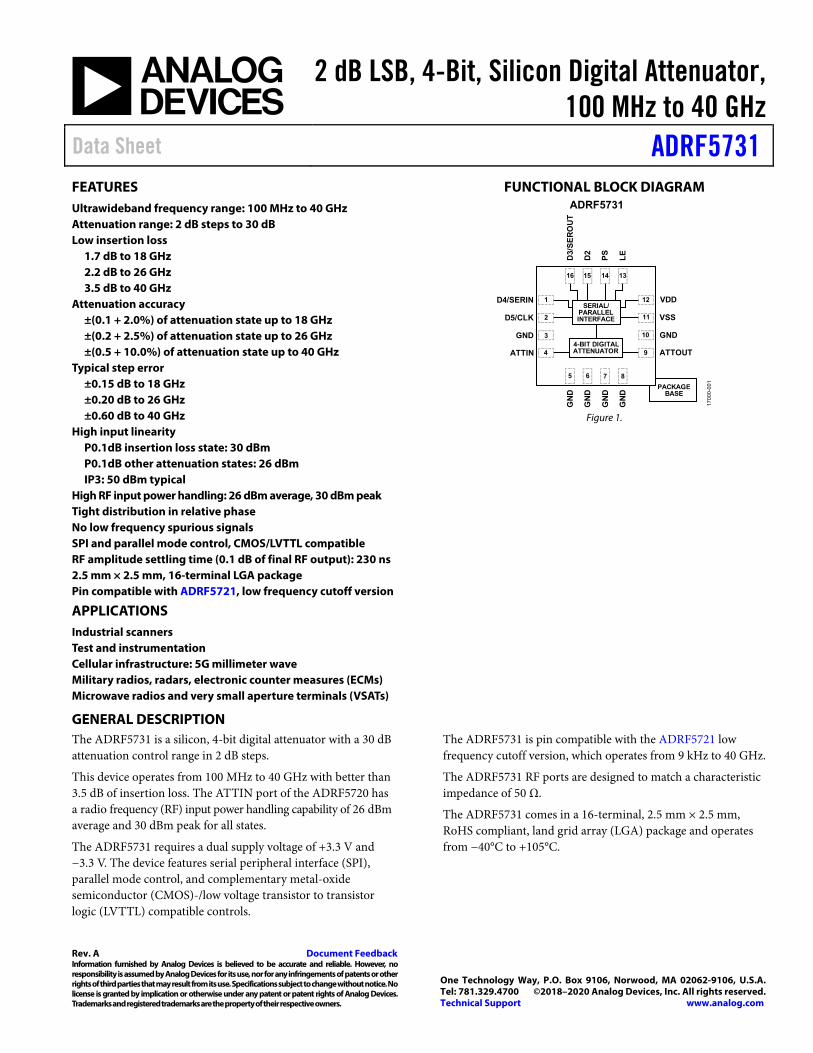
FUNCTIONAL BLOCK DIAGRAM
Figure 1.
GENERAL DESCRIPTION The ADRF5731 is a silicon, 4-bit digital attenuator with a 30 dB attenuation control range in 2 dB steps.
This device operates from 100 MHz to 40 GHz with better than 3.5 dB of insertion loss. The ATTIN port of the ADRF5720 has a radio frequency (RF) input power handling capability of 26 dBm average and 30 dBm peak for all states.
The ADRF5731 requires a dual supply voltage of +3.3 V and −3.3 V. The device features serial peripheral interface (SPI), parallel mode control, and complementary metal-oxide semiconductor (CMOS)-/low voltage transistor to transistor logic (LVTTL) compatible controls.
The ADRF5731 is pin compatible with the ADRF5721 low frequency cutoff version, which operates from 9 kHz to 40 GHz.
The ADRF5731 RF ports are designed to match a characteristic impedance of 50 Ω.
The ADRF5731 comes in a 16-terminal, 2.5 mm × 2.5 mm, RoHS compliant, land grid array (LGA) package and operates from −40°C to +105°C.
PACKAGEBASE
SERIAL/PARALLELINTERFACE
4-BIT DIGITALATTENUATOR
D2
D3/
SE
RO
UT
GN
D
GN
D
GN
D
GN
D
VDDD4/SERIN
VSS
GND
ADRF5731
ATTOUT
1
D5/CLK 2
GND 3
ATTIN 4
12
11
10
9
65 7 8
16 15
PS
LE
14 13
170
00
-001

ADRF5731 Data Sheet
Rev. A | Page 2 of 17
TABLE OF CONTENTS Features .............................................................................................. 1
Applications ....................................................................................... 1
Functional Block Diagram .............................................................. 1
General Description ......................................................................... 1
Revision History ............................................................................... 2
Specifications ..................................................................................... 3
Electrical Specifications ............................................................... 3
Timing Specifications .................................................................. 5
Absolute Maximum Ratings ....................................................... 6
Thermal Resistance ...................................................................... 6
Power Derating Curves ................................................................ 6
ESD Caution .................................................................................. 6
Pin Configuration and Function Descriptions ............................. 7
Interface Schematics..................................................................... 7
Typical Performance Characteristics ............................................. 8
Insertion Loss, Return Loss, State Error, Step Error, and Relative Phase ................................................................................8
Input Power Compression and Third-Order Intercept ......... 10
Theory of Operation ...................................................................... 11
Power Supply ............................................................................... 11
RF Input and Output ................................................................. 11
Serial or Parallel Mode Selection ............................................. 12
Serial Mode Interface ................................................................. 12
Parallel Mode Interface .............................................................. 13
Applications Information .............................................................. 14
Evaluation Board ........................................................................ 14
Probe Matrix Board ................................................................... 16
Packaging and Ordering Information ......................................... 17
Outline Dimensions ................................................................... 17
Ordering Guide .......................................................................... 17
REVISION HISTORY 3/2020—Rev. 0 to Rev. A Changes to RF Power Parameter, Table 1 ...................................... 4 Changes to Table 3 ............................................................................ 6 Changes to Power Supply Section ................................................ 11 Added Power-Up State Section ..................................................... 11 Moved Serial or Parallel Mode Selection Section and Table 7; Renumbered Sequentially ...................................................................... 12 9/2018—Revision 0: Initial Version

Data Sheet ADRF5731
Rev. A | Page 3 of 17
SPECIFICATIONS ELECTRICAL SPECIFICATIONS VDD = 3.3 V, VSS = −3.3 V, digital voltages = 0 V or VDD, case temperature (TCASE) = 25°C, and a 50 Ω system, unless otherwise noted.
Table 1. Parameter Test Conditions/Comments Min Typ Max Unit FREQUENCY RANGE 100 40,000 MHz INSERTION LOSS (IL) 100 MHz to 10 GHz 1.3 dB 10 GHz to 18 GHz 1.7 dB 18 GHz to 26 GHz 2.2 dB 26 GHz to 35 GHz 2.8 dB 35 GHz to 40 GHz 3.5 dB RETURN LOSS ATTIN and ATTOUT, all attenuation states 100 MHz to 10 GHz 22 dB 10 GHz to 18 GHz 22 dB 18 GHz to 26 GHz 16 dB 26 GHz to 35 GHz 15 dB 35 GHz to 40 GHz 14 dB ATTENUATION
Range Between minimum and maximum attenuation states
30 dB
Step Size Between any successive attenuation states 2 dB Accuracy Referenced to insertion loss
100 MHz to 10 GHz ±(0.05 + 1.0%) dB 10 GHz to 18 GHz ±(0.1 + 2.0%) dB 18 GHz to 26 GHz ±(0.2 + 2.5%) dB 26 GHz to 35 GHz ±(0.2 + 6.0%) dB 35 GHz to 40 GHz ±(0.5 + 10.0%) dB Step Error Between any successive attenuation states 100 MHz to 10 GHz ±0.05 dB 10 GHz to 18 GHz ±0.15 dB 18 GHz to 26 GHz ±0.20 dB 26 GHz to 35 GHz ±0.35 dB 35 GHz to 40 GHz ±0.60 dB
RELATIVE PHASE Referenced to insertion loss 100 MHz to 10 GHz 15 Degrees 10 GHz to 18 GHz 25 Degrees 18 GHz to 26 GHz 40 Degrees 26 GHz to 35 GHz 55 Degrees 35 GHz to 40 GHz 80 Degrees SWITCHING CHARACTERISTICS All attenuation states at input power (PIN) = 10 dBm
Rise and Fall Time (tRISE and tFALL) 10% to 90% of RF output 35 ns On and Off Time (tON and tOFF) 50% triggered control (CTL) to 90% of RF output 110 ns RF Amplitude Settling Time
0.1 dB 50% triggered CTL to 0.1 dB of final RF output 230 ns 0.05 dB 50% triggered CTL to 0.05 dB of final RF output 250 ns
Overshoot 0.5 dB Undershoot −1 dB RF Phase Settling Time f = 5 GHz
5° 50% triggered CTL to 5° of final RF output 100 ns 1° 50% triggered CTL to 1°of final RF output 125 ns

ADRF5731 Data Sheet
Rev. A | Page 4 of 17
Parameter Test Conditions/Comments Min Typ Max Unit INPUT LINEARITY1 10 MHz to 30 GHz
0.1 dB Power Compression (P0.1dB) Insertion Loss State 30 dBm Other Attenuation States 26 dBm
Third-Order Intercept (IP3) Two-tone input power = 14 dBm per tone, Δf = 1 MHz, all attenuation states
50 dBm
DIGITAL CONTROL INPUTS LE, PS, D2, D3/SEROUT,2 D4/SERIN, D5/CLK pins Voltage
Low (VINL) 0 0.8 V High (VINH) 1.2 3.3 V
Current Low (IINL) <1 μA High (IINH) D2 33 μA LE, PS, D3/SEROUT,2 D4/SERIN, D5/CLK pins <1 μA
DIGITAL CONTROL OUTPUT D3/SEROUT pin2 Voltage
Low (VOUTL) 0 ± 0.3 V High (VOUTH) VDD ± 0.3 V
Low and High Current (IOUTL, IOUTH) 0.5 mA SUPPLY CURRENT VDD and VSS pins
Positive 117 μA Negative −117 μA
RECOMMENDED OPERATING CONDITIONS Supply Voltage
Positive (VDD) 3.15 3.45 V Negative (VSS) −3.45 −3.15 V
Digital Control Voltage 0 VDD V RF Power3 f = 10 MHz to 30 GHz, TCASE = 85°C,4
all attenuation states
Input at ATTIN Steady state average 26 dBm Steady state peak 30 dBm Hot switching average 24 dBm Hot switching peak 27 dBm Input at ATTOUT Steady state average 18 dBm Steady state peak 21 dBm Hot switching average 15 dBm Hot switching peak 18 dBm
Case Temperature (TCASE) −40 +105 °C 1 Input linearity performance degrades over frequency (see Figure 20 and Figure 21). 2 The D3/SEROUT pin is an input in parallel control mode and an output in serial control mode. See Table 5 for the pin function descriptions. 3 For power derating over frequency, see Figure 2 and Figure 3. Applicable for all ATTIN and ATTOUT power specifications. 4 For 105°C operation, the power handling degrades from the TCASE = 85°C specifications by 3 dB.

Data Sheet ADRF5731
Rev. A | Page 5 of 17
TIMING SPECIFICATIONS See Figure 24, Figure 25, and Figure 26 for the timing diagrams.
Table 2. Parameter Description Min Typ Max Unit tSCK Minimum serial period, see Figure 24 70 ns tCS Control setup time, see Figure 24 15 ns tCH Control hold time, see Figure 24 20 ns tLN LE setup time, see Figure 24 15 ns tLEW Minimum LE pulse width, see Figure 24 and Figure 26 10 ns tLES Minimum LE pulse spacing, see Figure 24 630 ns tCKN Serial clock hold time from LE, see Figure 24 0 ns tPH Hold time, see Figure 26 10 ns tPS Setup time, see Figure 26 2 ns tCO Clock to output (SEROUT) time, see Figure 25 20 ns

ADRF5731 Data Sheet
Rev. A | Page 6 of 17
ABSOLUTE MAXIMUM RATINGS Table 3. Parameter Rating Positive Supply Voltage (VDD) −0.3 V to +3.6 V Negative Supply Voltage (VSS) −3.6 V to +0.3 V Digital Control Inputs
Voltage −0.3 V to VDD + 0.3 V Current 3 mA
RF Power1 (f = 10 MHz to 30 GHz, TCASE = 85°C2)
Input at ATTIN Steady State Average 27 dBm Steady State Peak 31 dBm Hot Switching Average 25 dBm Hot Switching Peak 28 dBm
Input at ATTOUT Steady State Average 19 dBm Steady State Peak 22 dBm Hot Switching Average 16 dBm Hot Switching Peak 19 dBm
RF Power Under Unbiased Condition (VDD, VSS = 0 V)
Input at ATTIN 21 dBm Input at ATTOUT 15 dBm
Temperature Junction (TJ) 135°C Storage −65°C to +150°C Reflow 260°C
Continuous Power Dissipation (PDISS) 0.5 W Electrostatic Discharge (ESD) Sensitivity
Human Body Model (HBM) ATTIN and ATTOUT Pins 500 V Digital Pins 2000 V
Charged Device Model (CDM) 1250 V
1 For power derating over frequency, see Figure 2 and Figure 3. Applicable for all ATTIN and ATTOUT power specifications.
2 For 105°C operation, the power handling derates from the TCASE = 85°C specifications by 3 dB.
Stresses at or above those listed under Absolute Maximum Ratings may cause permanent damage to the product. This is a stress rating only; functional operation of the product at these or any other conditions above those indicated in the operational section of this specification is not implied. Operation beyond the maximum operating conditions for extended periods may affect product reliability.
THERMAL RESISTANCE Thermal performance is directly linked to printed circuit board (PCB) design and operating environment. Careful attention to PCB thermal design is required.
θJC is the junction to case bottom (channel to package bottom) thermal resistance.
Table 4. Thermal Resistance Package Type θJC Unit CC-16-6 100 °C/W
POWER DERATING CURVES
Figure 2. Power Derating vs. Frequency, Low Frequency Detail, TCASE = 85°C
Figure 3. Power Derating vs. Frequency, High Frequency Detail, TCASE = 85°C
ESD CAUTION
2
–16
–14
–12
–10
–8
–6
–4
–2
0
1k 10k 100G10G100M1M 1G10M100k
PO
WE
R D
ER
AT
ING
(d
B)
FREQUENCY (Hz) 17
000
-00
2
2
–16
–14
–12
–10
–8
–6
–4
–2
0
26 50484634 4028 36 4230 38 4432
PO
WE
R D
ER
AT
ING
(d
B)
FREQUENCY (GHz) 17
000
-00
3

Data Sheet ADRF5731
Rev. A | Page 7 of 17
PIN CONFIGURATION AND FUNCTION DESCRIPTIONS
Figure 4. Pin Configuration
Table 5. Pin Function Descriptions Pin No. Mnemonic Description 1 D4/SERIN Parallel Control Input for 8 dB Attenuator Bit (D4). Serial Data Input (SERIN). See the Theory of Operation section for more information. 2 D5/CLK Parallel Control Input for 16 dB Attenuator Bit (D5). Serial Clock Input (CLK). See the Theory of Operation section for more information. 3, 5 to 8, 10 GND Ground. These pins must be connected to the RF and dc ground of the PCB. 4 ATTIN Attenuator Input. This pin is dc-coupled to 0 V and ac matched to 50 Ω. No dc blocking capacitor is needed
when the RF line potential is equal to 0 V dc. 9 ATTOUT Attenuator Output. This pin is dc-coupled to 0 V and ac matched to 50 Ω. No dc blocking capacitor is needed
when the RF line potential is equal to 0 V dc. 11 VSS Negative Supply Input. 12 VDD Positive Supply Input. 13 LE Latch Enable Input. See the Theory of Operation section for more information. 14 PS Parallel or Serial Control Interface Selection Input. See the Theory of Operation section for more information. 15 D2 Parallel Control Input for 2 dB Attenuator Bit. See the Theory of Operation section for more information. 16 D3/SEROUT Parallel Control Input for 4 dB Attenuator Bit (D3). Serial Data Output (SEROUT). See the Theory of Operation section for more information. 17 EPAD Exposed Pad. The exposed pad must be connected to the RF and dc ground of the PCB.
INTERFACE SCHEMATICS
Figure 5. Digital Input Interface Schematic for LE, PS, D3/SEROUT, D4/SERIN,
and D5/CLK
Figure 6. ATTIN and ATTOUT Interface Schematic
Figure 7. Digital Input Interface Schematic for D2
D2
D3/
SE
RO
UT
GN
D
GN
D
GN
D
GN
D
VDDD4/SERIN
VSS
GND
ATTOUT
D5/CLK
GND
ATTIN
PS
LE
ADRF5731TOP VIEW
(Not to Scale)
17
000
-00
4NOTES1. EXPOSED PAD. THE EXPOSED PAD MUST BE CONNECTED TO THE RF AND DC GROUND OF THE PCB.
1
2
3
4
12
11
10
9
65 7 8
16 15 14 13
VDDVDD
LE, PS, D3/SEROUT,D4/SERIN, D5/CLK
17
00
0-0
05
ATTIN,ATTOUT
17
00
0-0
06
VDDVDD
100kΩ
D2
17
00
0-0
07

ADRF5731 Data Sheet
Rev. A | Page 8 of 17
TYPICAL PERFORMANCE CHARACTERISTICS INSERTION LOSS, RETURN LOSS, STATE ERROR, STEP ERROR, AND RELATIVE PHASE VDD = 3.3 V, VSS = −3.3 V, digital voltages = 0 V or VDD, TCASE = 25°C, and a 50 Ω system, unless otherwise noted. Measured on probe matrix board using ground signal ground (GSG) probes close to the RF pins (ATTIN and ATTOUT). See the Applications Information section for details on evaluation and probe matrix boards.
Figure 8. Insertion Loss vs. Frequency over Temperature
Figure 9. Normalized Attenuation vs. Frequency for All States at Room Temperature
Figure 10. Input Return Loss vs. Frequency (Major States Only)
Figure 11. Output Return Loss vs. Frequency (Major States Only)
Figure 12. Step Error vs. Frequency (Major States Only)
Figure 13. Step Error vs. Attenuation State over Frequency
–10
–9
–8
–7
–6
–5
–4
–3
–2
–1
0
0 5 10 15 20 25 30 35 40 45
INS
ER
TIO
N L
OS
S (
dB
)
FREQUENCY (GHz)
+105°C
+25°C–40°C
+85°C
17
000
-00
8
0 5 10 15 20 25 30 35 40 45
NO
RM
AL
IZE
D A
TT
EN
UA
TIO
N (
dB
)
FREQUENCY (GHz)
–35
–30
–25
–20
–15
–10
–5
0
17
000
-00
9
0 5 10 15 20 25 30 35 40 45
FREQUENCY (GHz)
–50
–45
–40
–35
–30
–25
–20
–15
–10
–5
0
INP
UT
RE
TU
RN
LO
SS
(dB
)
17
000
-01
0
STATE 0dB STATE 2dBSTATE 4dB STATE 8dBSTATE 16dB STATE 30dB
0 5 10 15 20 25 30 35 40 45
FREQUENCY (GHz)
–50
–45
–40
–35
–30
–25
–20
–15
–10
–5
0
OU
TP
UT
RE
TU
RN
LO
SS
(dB
)
17
000
-011
STATE 0dB STATE 2dBSTATE 4dB STATE 8dBSTATE 16dB STATE 30dB
0 5 10 15 20 25 30 35 40 45
ST
EP
ER
RO
R (
dB
)
FREQUENCY (GHz)
–1.5
–1.0
–0.5
0
0.5
1.0
1.5
17
000
-01
2
STATE 0dB STATE 2dBSTATE 4dB STATE 8dBSTATE 16dB STATE 30dB
ST
EP
ER
RO
R (
dB
)
ATTENUATION STATE
–1.5
–1.0
–0.5
0
0.5
1.0
1.5
0 2 4 6 8 10 12 14 16 18 20 22 24 26 28 30
5GHz 10GHz 15GHz20GHz 25GHz 30GHz35GHz 40GHz 45GHz
17
000
-01
3

Data Sheet ADRF5731
Rev. A | Page 9 of 17
Figure 14. State Error vs. Frequency (Major States Only)
Figure 15. State Error vs. Attenuation State over Frequency
Figure 16. Relative Phase vs. Frequency (Major States Only)
Figure 17. Relative Phase vs. Attenuation State over Frequency
0 5 10 15 20 25 30 35 40 45
FREQUENCY (GHz)
–1
1
2
3
4
5
6
7
8
9
0
ST
AT
E E
RR
OR
(dB
)
17
000
-01
4
STATE 0dB STATE 2dBSTATE 4dB STATE 8dBSTATE 16dB STATE 30dB
ST
AT
E E
RR
OR
(d
B)
ATTENUATION STATE
0 2 4 6 8 10 12 14 16 18 20 22 24 26 28 30
5GHz 10GHz 15GHz20GHz 25GHz 30GHz35GHz 40GHz 45GHz
–1
1
2
3
4
5
6
7
8
9
0
17
000
-01
5
0 5 10 15 20 25 30 35 40 45
FREQUENCY (GHz)
0
20
30
40
50
60
70
80
90
100
10
RE
LA
TIV
E P
HA
SE
(Deg
rees
)
17
000
-01
6
STATE 0dB STATE 2dBSTATE 4dB STATE 8dBSTATE 16dB STATE 30dB
0
20
30
40
50
60
70
80
90
100
10
RE
LA
TIV
E P
HA
SE
(Deg
rees
)
ATTENUATION STATE
0 2 4 6 8 10 12 14 16 18 20 22 24 26 28 30
5GHz 10GHz 15GHz20GHz 25GHz 30GHz35GHz 40GHz 45GHz
17
000
-01
7

ADRF5731 Data Sheet
Rev. A | Page 10 of 17
INPUT POWER COMPRESSION AND THIRD-ORDER INTERCEPT
Figure 18. Input P0.1dB vs. Frequency (Major States Only)
Figure 19. Input IP3 vs. Frequency (Major States Only)
Figure 20. Input P0.1dB vs. Frequency (Major States Only), Low Frequency Detail
Figure 21. Input IP3 vs. Frequency (Major States Only), Low Frequency Detail
0
5
10
15
20
25
30
35
0 5 10 15 20 25 30 35 40
INP
UT
P0.
1dB
(d
Bm
)
FREQUENCY (GHz)
STATE 0dB STATE 2dBSTATE 4dB STATE 8dBSTATE 16dB STATE 30dB
17
000
-01
8
0
10
20
30
40
50
60
80
70
0 5 10 15 20 25 30 35 40
INP
UT
IP
3 (d
Bm
)
FREQUENCY (GHz)
STATE 0dB STATE 2dBSTATE 4dB STATE 8dBSTATE 16dB STATE 30dB
16
999
-01
9
0
5
10
15
20
25
30
35
10k 100k 1M 10M 100M 1G
INP
UT
P0.
1dB
(d
Bm
)
FREQUENCY (Hz)
STATE 0dB STATE 2dBSTATE 4dB STATE 8dBSTATE 16dB STATE 30dB
17
000
-02
0
10k 100k 1M 10M 100M 1G
FREQUENCY (Hz)
STATE 0dB STATE 2dBSTATE 4dB STATE 8dBSTATE 16dB STATE 30dB
17
000
-02
1
0
10
20
30
40
50
60
80
70
INP
UT
IP
3 (d
Bm
)

Data Sheet ADRF5731
Rev. A | Page 11 of 17
THEORY OF OPERATION The ADRF5731 incorporates a 4-bit fixed attenuator array that offers an attenuation range of 30 dB in 2 dB steps. An integrated driver provides both serial and parallel mode control of the attenuator array (see Figure 22).
Note that when referring to a single function of a multifunction pin in this section, only the portion of the pin name that is relevant is mentioned. For full pin names of the multifunction pins, refer to the Pin Configuration and Function Descriptions section.
POWER SUPPLY Bypassing capacitors are recommended on the positive supply voltage line (VDD) and negative supply line (VSS) to filter high frequency noise.
The power-up sequence is as follows:
1. Connect GND. 2. Power up the VDD and VSS voltages. Power up VSS after
VDD to avoid current transients on VDD during ramp-up. 3. Power up the digital control inputs. The order of the digital
control inputs is not important. However, powering the digital control inputs before the VDD voltage supply may inadvertently forward bias and damage the internal ESD structures. To avoid this damage, use a series 1 kΩ resistor to limit the current flowing in to the control pin. Use pull-
up or pull-down resistors if the controller output is in a high impedance state after the VDD voltage is powered up and the control pins are not driven to a valid logic state.
4. Apply an RF input signal to ATTIN or ATTOUT.
The power-down sequence is the reverse order of the power-up sequence.
Power-Up State
The ADRF5731 has internal power-on reset circuity. This circuity sets the attenuator to maximum attenuation state (30 dB) when the VDD and VSS voltages are applied and LE is set to low.
RF INPUT AND OUTPUT Both RF ports (ATTIN and ATTOUT) are dc-coupled to 0 V. DC blocking is not required at the RF ports when the RF line potential is equal to 0 V.
The RF ports are internally matched to 50 Ω. Therefore, external matching components are not required.
The ADRF5731 supports bidirectional operation at a lower power level. The power handling of the ATTIN and ATTOUT ports are different. Therefore, the bidirectional power handling is defined by the ATTOUT port. Refer to the RF input power specifications in Table 1.
Table 6. Truth Table Digital Control Input1
Attenuation State (dB) D5 D4 D3 D2 D1 D0 Low Low Low Low Don’t care Don’t care 0 (reference) Low Low Low High Don’t care Don’t care 2 Low Low High Low Don’t care Don’t care 4 Low High Low Low Don’t care Don’t care 8 High Low Low Low Don’t care Don’t care 16 High High High High Don’t care Don’t care 30
1 Any combination of the control voltage input states shown in Table 6 provides an attenuation equal to the sum of the bits selected.
Figure 22. Simplified Circuit Diagram
D Q D Q D Q D QD Q
PARALLEL OR SERIAL SELECT
6-BIT OR 8-BIT LATCH
D QDSERIN
CLK
PS
LE
D2 D3 D4 D5
QD Q
RFINPUT
RFOUTPUT
SEROUT
2dB 4dB 8dB 16dB
17
00
0-0
22
ADRF5731 Data Sheet
Rev. A | Page 12 of 17
SERIAL OR PARALLEL MODE SELECTION The ADRF5731 can be controlled in either serial or parallel mode by setting the PS pin to high or low, respectively (see Table 7).
Table 7. Mode Selection PS Control Mode Low Parallel High Serial
SERIAL MODE INTERFACE The ADRF5731 supports a 3-wire SPI: serial data input (SERIN), clock (CLK), and latch enable (LE). The serial control interface is activated when PS is set to high.
The ADRF5731 attenuation state is controlled by Bits[D5:D2]. Bit D0 and Bit D1 are don't care bits but must be input. Therefore, at least a 6-bit SERIN must be used to control the attenuation states. If using an 8-bit word to control the state of the attenuator, [D7:D6] and [D1:D0] are don’t care bits. It does not matter if these bits are held low or high. Refer to Table 6 and Figure 24 for additional information.
In serial mode, the SERIN data is clocked most significant bit (MSB) first on the rising CLK edges into the shift register. Then, LE must be toggled high to latch the new attenuation state into the device. LE must be set to low to clock new SERIN data into the shift register as CLK is masked to prevent the attenuator value from changing if LE is kept high. See Figure 24 in conjunction with Table 2 and Table 6.
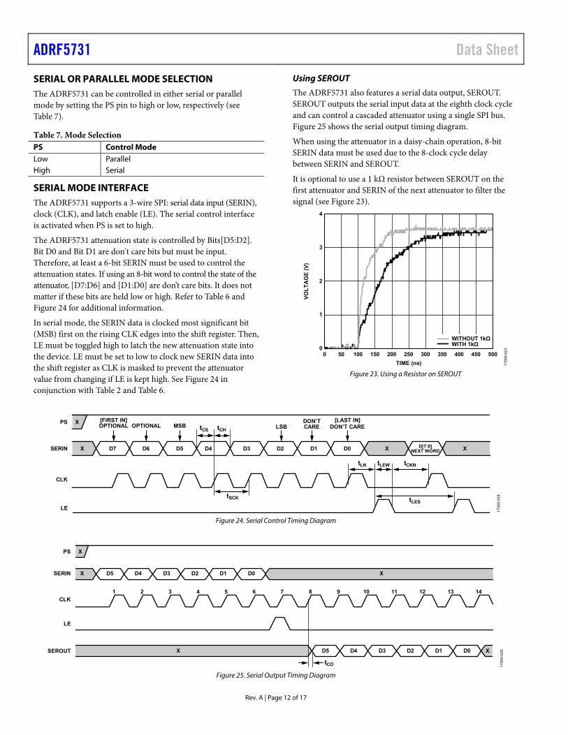
Using SEROUT
The ADRF5731 also features a serial data output, SEROUT. SEROUT outputs the serial input data at the eighth clock cycle and can control a cascaded attenuator using a single SPI bus. Figure 25 shows the serial output timing diagram.
When using the attenuator in a daisy-chain operation, 8-bit SERIN data must be used due to the 8-clock cycle delay between SERIN and SEROUT.
It is optional to use a 1 kΩ resistor between SEROUT on the first attenuator and SERIN of the next attenuator to filter the signal (see Figure 23).
Figure 23. Using a Resistor on SEROUT
Figure 24. Serial Control Timing Diagram
Figure 25. Serial Output Timing Diagram
4
3
2
1
00 200100 300 400 50015050 250 350 450
VO
LT
AG
E (
V)
TIME (ns)
WITHOUT 1kΩWITH 1kΩ
170
00
-023
X
X
SERIN
CLK
LE
PS
D7 D6 D5 D4 D3 D2 D1 D0 X XD[7:0]NEXT WORD
[FIRST IN]OPTIONAL
[LAST IN]DON’T CARE
DON’TCARELSBOPTIONAL MSB tCS tCH
tSCK
tLN tCKN
tLES
tLEW
17
00
0-0
24
X
SERIN
CLK
LE
SEROUT
PS
D5X D4 D3 D2 D1 D0
D5X D4 D3 D2 D1 D0 X
X
1 2 3 4 5 6 7 8 9 10 11 12 13 14
tCO 17
000
-02
5

Data Sheet ADRF5731
Rev. A | Page 13 of 17
PARALLEL MODE INTERFACE The ADRF5731 has four digital control inputs, D2 (LSB) to D5 (MSB), to select the desired attenuation state in parallel mode, as shown in Table 6. The parallel control interface is activated when PS is set to low.
There are two modes of parallel operation: direct parallel and latched parallel.
Direct Parallel Mode
To enable direct parallel mode, keep the LE pin high. To change the attenuation state, use the control voltage inputs (D2 to D5) directly. This mode is ideal for manual control of the attenuator.
Latched Parallel Mode
To enable latched parallel mode, keep the LE pin low when changing the control voltage inputs (D2 to D5) to set the attenuation state. When the desired state is set, toggle LE high to transfer the 4-bit data to the bypass switches of the attenuator array and then toggle LE low to latch the change into the device until the next desired attenuation change (see Figure 26 in conjunction with Table 2).
Figure 26. Latched Parallel Mode Timing Diagram
D5 TO D2
PS
LE
tPS tPH
tLEW
X X
X
17
00
0-0
26

ADRF5731 Data Sheet
Rev. A | Page 14 of 17
APPLICATIONS INFORMATION EVALUATION BOARD The ADRF5731-EVALZ is a 4-layer evaluation board. The top and bottom copper layer are 0.5 oz (0.7 mil) plated to 1.5 oz (2.2 mil) and are separated by dielectric materials. The stackup for this evaluation board is shown in Figure 27.
Figure 27. Evaluation Board Stackup, Cross Sectional View
All RF and dc traces are routed on the top copper layer, whereas the inner and bottom layers are grounded planes that provide a solid ground for the RF transmission lines. The top dielectric material is 12 mil Rogers RO4003, offering optimal high frequency performance. The middle and bottom dielectric materials provide mechanical strength. The overall board thickness is 62 mil, which allows 2.4 mm RF launchers to be connected at the board edges.
The RF transmission lines are designed using a coplanar waveguide (CPWG) model, with a trace width of 16 mil and ground clearance of 6 mil to have a characteristic impedance of 50 Ω. For optimal RF and thermal grounding, as many through vias as possible are arranged around transmission lines and under the exposed pad of the package.
Thru calibration can be used to calibrate out the board loss effects from the ADRF5731-EVALZ evaluation board measurements to determine the device performance at the pins of the IC. Figure 28 shows the typical board loss (THRU) for the ADRF5731-EVALZ evaluation board at room temperature, the embedded insertion loss, and the de-embedded insertion loss for the ADRF5731.
Figure 28. Insertion Loss vs. Frequency
Figure 29 shows the actual ADRF5731-EVALZ evaluation board with component placement.
Figure 29. Evaluation Board Layout, Top View
Two power supply ports are connected to the VDD and VSS test points, TP1 and TP2, and the ground reference is connected to the GND test point, TP4. On the supply traces, VDD and VSS, use a 100 pF bypass capacitor to filter high frequency noise. Additionally, unpopulated components positions are available for applying extra bypass capacitors.
All the digital control pins are connected through digital signal traces to the 2 × 9-pin header, P1. There are provisions for a resistor capacitor (RC) filter that helps eliminate dc-coupled noise. The ADRF5731 was evaluated without an external RC filter, the series resistors are 0 Ω, and shunt capacitors are unpopulated on the evaluation board.
The RF input and output ports (ATTIN and ATTOUT) are connected through 50 Ω transmission lines to the 2.4 mm RF launchers, J1 and J2, respectively. These high frequency RF launchers are connected by contact and are not soldered onto the board.
A thru calibration line connects the unpopulated J3 and J4 launchers. This transmission line is used to estimate the loss of the PCB over the environmental conditions being evaluated.
The schematic of the ADRF5731-EVALZ evaluation board is shown in Figure 30.
RO4003
1.5oz Cu (2.2mil)1.5oz Cu (2.2mil)
0.5oz Cu (0.7mil)
TO
TA
L T
HIC
KN
ES
S~
62m
il
0.5oz Cu (0.7mil)
1.5oz Cu (2.2mil)
1.5oz Cu (2.2mil)
W = 16milG = 6mil
T = 2.2mil
H = 12mil
170
00
-02
7
–10
–9
–8
–7
–6
–5
–4
–3
–2
–1
0
0 5 10 15 20 25 30 35 40 45
INS
ER
TIO
N L
OS
S (
dB
)
FREQUENCY (GHz)
THRU LOSSDE-EMBEDDED INSERTION LOSSEMBEDDED INSERTION LOSS
17
000
-02
8
17
00
0-0
29

Data Sheet ADRF5731
Rev. A | Page 15 of 17
Figure 30. Evaluation Board Schematic
Table 8. Evaluation Board Components Component Default Value Description C1, C2 100 pF Capacitors, C0402 package J1, J2 Not applicable 2.4 mm end launch connectors (Southwest Microwave: 1492-04A-6) P1 Not applicable 2 × 9-pin header R1 to R6 0 Ω Resistors, 0402 package TP1, TP2, TP4 Not applicable Through hole mount test points U1 ADRF5731 ADRF5731 digital attenuator, Analog Devices, Inc.
D4/SERIN
EPAD
D5/CLK
GND
ATTIN
1
2
3
4
12
11
10
9
VDD
D4_SERIN R4
0Ω
VSS
GND
ATTOUT
GN
D
GN
D
GN
D
GN
D
1315 1416
6 75 8L
E
D3/
SE
RO
UT
PS
D2
ADRF5731
17
D5_CLK
ATTIN ATTOUTJ2
THRU CAL
J3DNI
J4DNI
J1
R3
0Ω
PSR1
0Ω
LE
VDDTP1
C1100pF
VSSTP2
C2100pF
R2
0ΩD3_SEROUT
0Ω
R5
D2
0Ω
R6 26
13
48
57
1012
9PS
P1
LE
D5_CLKD4_SERIND3_SEROUT
D2
GNDTP4
111416
1315
1817
170
00
-030

ADRF5731 Data Sheet
Rev. A | Page 16 of 17
PROBE MATRIX BOARD The probe matrix board is a 4-layer board. Similar to the evaluation board, the probe matrix board also uses a 12 mil Rogers RO4003 dielectric. The top and bottom copper layers are 0.5 oz (0.7 mil) plated to 1.5 oz (2.2 mil). The RF transmission lines are designed using a CPWG model with a width of 16 mil and ground spacing of 6 mil to have a characteristic impedance of 50 Ω.
Figure 31 and Figure 32 show the cross sectional view and the top view of the board, respectively. Measurements are made using GSG probes at close proximity to the RF pins (ATTIN and ATTOUT). Unlike the evaluation board, probing reduces reflections caused by mismatch arising from connectors, cables, and board layout, resulting in a more accurate measurement of the device performance.
Figure 31. Probe Matrix Board (Cross Sectional View)
Figure 32. Probe Matrix Board Layout (Top View)
The probe matrix board includes a thru reflect line (TRL) calibration kit, allowing board loss de-embedding. The actual board duplicates the same layout in matrix form to assemble multiple devices at one time. Figure 33 is a detailed image of the trace to pin transition with corresponding dimensions. All S parameters were measured on this board.
Figure 33. Probe Board Layout Dimensions (Top View)
RO4003
1.5oz Cu (2.2mil)1.5oz Cu (2.2mil)
0.5oz Cu (0.7mil)
TO
TA
L T
HIC
KN
ES
S~
62m
il
0.5oz Cu (0.7mil)
1.5oz Cu (2.2mil)
1.5oz Cu (2.2mil)
W = 16milG = 6mil
T = 2.2mil
H = 12mil
170
00
-03
1
17
00
0-0
32
17
00
0-0
33
8mil
16m
il
16mil

Data Sheet ADRF5731
Rev. A | Page 17 of 17
PACKAGING AND ORDERING INFORMATION OUTLINE DIMENSIONS
Figure 34. 16-Terminal Land Grid Array [LGA]
2.5 mm × 2.5 mm Body and 0.75 mm Package Height (CC-16-6)
Dimensions shown in millimeters
ORDERING GUIDE Model1 Temperature Range Package Description Package Option Marking Code ADRF5731BCCZN −40°C to +105°C 16-Terminal Land Grid Array [LGA] CC-16-6 31 ADRF5731BCCZN-R7 −40°C to +105°C 16-Terminal Land Grid Array [LGA] CC-16-6 31 ADRF5731-EVALZ Evaluation Board 1 Z = RoHS Compliant Part.
0
4-1
4-2
017
-A
PK
G-0
05
30
9
2.602.50 SQ2.40
TOP VIEW
SIDE VIEW
BOTTOM VIEW
1
4
58
9
12
13 16
1.101.00 SQ0.90
0.40BSC
0.125REF
1.20 REF
0.2500.2000.150
0.3250.2750.225
0.8500.7500.650
0.2600.2200.180
FOR PROPER CONNECTION OFTHE EXPOSED PADS, REFER TOTHE PIN CONFIGURATION ANDFUNCTION DESCRIPTIONSSECTION OF THIS DATA SHEET.
EXPOSEDPAD
0.530 REF
CHAMFEREDPIN 1 (0.1 × 45°)
PIN 1CORNER AREA
©2018–2020 Analog Devices, Inc. All rights reserved. Trademarks and registered trademarks are the property of their respective owners.
D17000-3/20(A) www.analog.com/ADRF5731