2. modeling sequential logic with verilog - · pdf fileintroduction to verilog 2. modeling...
TRANSCRIPT
Introduction to Verilog
2. Modeling Sequential Logic with Verilog
This section introduces some basic models of sequential logic using Verilog. Flip-flops are the basic logic elements used in sequential logic. Registers are constructed using one or more flip-flops which share common signals such as the clock. Our discussion will focus on behavioral models.
Behavioral models are typically used to model flip-flops in Verilog. An always procedural block with event control in the form of a sensitivity list is used to determine when the state of the flip-flop changes. If-else or case statements in the procedural block are then used to determine the next state.
Latches can also be modeled in Verilog, either by a structural model based on gates or behaviorally as we do in the following with flip-flops. However, the use of latches is typically avoided when synthesizing Verilog for an FPGA as the timing is difficult to analyze.
2.1. Modeling Flip-flops
Flip-flops are memory elements that change state on the active edge of a clock signal. A behavioral model of a flip-flop in Verilog uses an always construction to model this behavior. Evaluation of the procedural block which describes the behavior of a flip-flop is controlled by the sensitivity list. Verilog keywords posedge and negedge are qualifiers which can be used to specify the active edge of a clock signal. An example of an always block which models a simple D flip-flop is shown is the following
always @(posedge Clock)begin Q=D;end
This always statement will update Q with the value of D on the rising edge of the clock signal.
A synchronous active low clear signal can be added to this flip-flop model to reset the flip-flop output to 0. This is done with an if-else statement in the always block as follows
always @(posedge Clock)begin if (~ClearN) Q=1'b0; else Q=D;end
Here ClearN is a control signal which is sampled on the rising edge of the clock. If clear is 0 the argument in the if-else is 1 corresponding to true and the output Q of the flip-flop is set to 0, otherwise the output is updated with the value of D.
1
© 2015 Cengage Learning. All Rights Reserved. May not be scanned, copied or duplicated, or posted to a publicly accessible website, in whole or in part.
Introduction to Verilog
The Verilog if-else statement can only be used in procedural block. It operates in like the if-else construction in C. In general it takes the form
if ( expression ) true_statement_blockelse false_statement_block
If expression is true the statements in true_statement_block are executed, if not then the statements in false_statement_block are executed. In Verilog as in C, true corresponds to a nonzero value which is known and false corresponds to a zero value, x, or z. The number of statements associated with each branch can be zero, one, or more than one. If multiple statements are used they must be bracketed by begin-end to form a block statement.
An asynchronous clear signal could be used instead of a synchronous clear. In this case the always statement modeling the flip-flop is
always @(posedge Clock, negedge ClearN)begin if (~ClearN) Q=1'b0; else Q=D;end
Here the falling edge of ClearN initiates the evaluation of the always block. In contrast the synchronous clear does not initiate the evaluation, that is determined by the clock signal.
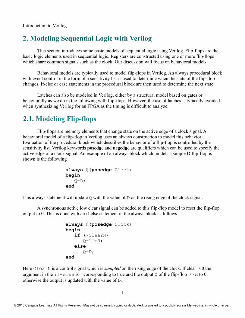
We can use this last to construct a Verilog module for the D flip-flop shown in figure 2.1.
Figure 2.1. D flip-flop with asynchonous low clear and complementary output
This D flip-flop shown has a single data input, D, and two data outputs, Q corresponding to the state and the complement of Q, QN. The D flip-flop shown has a clock input which causes the state to update on the rising edge and an asynchronous active low clear signal.
2
© 2015 Cengage Learning. All Rights Reserved. May not be scanned, copied or duplicated, or posted to a publicly accessible website, in whole or in part.
Introduction to Verilog
module DFF (Q,QN,D,Clock,ClearN); output Q,QN; // data output input D; // data input input Clock,Clear;
reg Q;
always @(posedge Clock, negedge ClearN) begin if (~Clear) Q=1'b0; else Q=D; end
assign QN = ~Q;
endmodule
Since there is only one statement in the always construction the begin and end statements are optional, we have chosen to use them. Since Q is updated inside the always statement it has been defined as a variable with the reg statement. Finally, the complement of the output, QN, is obtained by a continuous assignment statement.
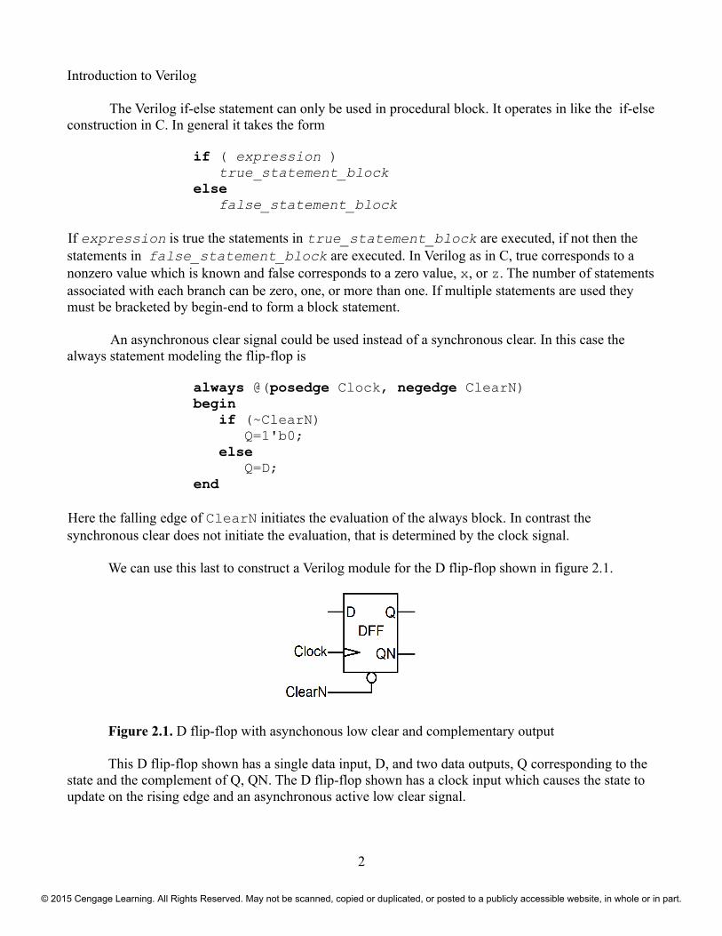
The J-K flip-flop has two inputs, J and K, which determine the next state on the active edge of the clock. If both J and K are 0 the state does not transition, if J is 1 and K is 0 then the state transitions to Q = 1, if J is 0 and K is 1 the state transitions to Q = 0, and if both J and K are 1 the state toggles so Q = Q. Denoting Q+ as the value of the next state this can be expressed as Q+ = J Q + K Q.
Figure 2.2. The J-K Flip-flop
The Verilog model of the D flip-flop can be modified to model the J-K flip-flop,
module JKFF (Q,QN,J,K,Clock); output Q, QN; // data output input J, K; // data input input Clock;
3
© 2015 Cengage Learning. All Rights Reserved. May not be scanned, copied or duplicated, or posted to a publicly accessible website, in whole or in part.

Introduction to Verilog
reg Q;
always @(posedge Clock) begin Q = J&(~Q)|(~K)&Q; end
assign QN = ~Q;
endmodule
A more straight forward way to model the J-K flip-flop is to directly implement the corresponding truth table and use the J and K inputs to control the behavior. We can use a series of nested if-else statements to implement this as,
module JKFF (Q,QN,J,K,Clock); output Q, QN; // data output input J, K; // data input input Clock;
reg Q;
always @(posedge Clock) begin if ({J,K} == 2'b01) Q = 1'b0; else if ({J,K} == 2'b10) Q = 1'b1; else if ({J,K} == 2'b11) Q = ~Q; else Q = Q; end
assign QN = ~Q;
endmodule
Here we have arranged the if-else statements so that the last else statement does not change the value of Q. Two things to note, the first is that for this model of the J-K flip-flop the last else statement will execute not only for J and K both zero but if either or both J and K are also x or z. We also note that while this model seems to be the same if or not we omit the last else, that when using if-else Verilog conditional statements it is good practice to specify explicitly all outcomes.
Another way to implement a truth table in Verilog is to use the case statement. The Verilog case statement is similar to the switch statement in C. Replacing the nested if-else statements in the above with the Verilog case construction we get
4
© 2015 Cengage Learning. All Rights Reserved. May not be scanned, copied or duplicated, or posted to a publicly accessible website, in whole or in part.
Introduction to Verilog
module JKFF (Q,QN,J,K,Clock); output Q, QN; // data output input J, K; // data input input Clock;
reg Q;
always @(posedge Clock) begin case ({J,K}) 2'b01: Q = 1'b0; 2'b10: Q = 1'b1; 2'b11: Q = ~Q; default: Q = Q; endcase end
assign QN = ~Q;
endmodule
In this case statement the 2-bit value is evaluated and the statement that is labeled with the corresponding value is executed. If no match is found then the statement labeled default is executed. Including the default label, just like including the final else branch in the if-else, allows us to explicitly specify all the outcomes in evaluating the case statement. Using default in a case statement is good practice. Note that in this example the case statement is considered a single statement so the begin and end are not needed, however we chose to include them.
The case statement has the general form:
case (expression) case1_identifier: statement1_block case2_identifier: statement2_block : default: default_statement_blockendcase
The case statement will attempt to match expression with the case identifiers. This comparison is done on a bitwise basis and includes bit values x and z. The comparisons are done in order, the first comparision is with case1_identifier, the next withcase2_identifier, and so forth down the list. If a match is made the corresponding statement block is executed. A statement block can be either a single statement or a group of statements bracketed by begin-end. The default label which is last on the list is optional. If no match has been made with any of the previous case identifiers then the default_statement_block is executed before exiting the case statement. For
5
© 2015 Cengage Learning. All Rights Reserved. May not be scanned, copied or duplicated, or posted to a publicly accessible website, in whole or in part.
Introduction to Verilog
completeness it is good practice to include default.
Two variants of the case statement are casez and casex. For casez a z is treated as a don't care while for casex both x and z are treated as don't cares.
2.2. Registers
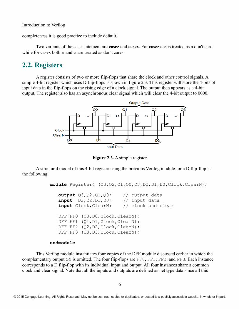
A register consists of two or more flip-flops that share the clock and other control signals. A simple 4-bit register which uses D flip-flops is shown in figure 2.3. This register will store the 4-bits of input data in the flip-flops on the rising edge of a clock signal. The output then appears as a 4-bit output. The register also has an asynchronous clear signal which will clear the 4-bit output to 0000.
Figure 2.3. A simple register
A structural model of this 4-bit register using the previous Verilog module for a D flip-flop is the following
module Register4 (Q3,Q2,Q1,Q0,D3,D2,D1,D0,Clock,ClearN);
output Q3,Q2,Q1,Q0; // output data input D3,D2,D1,D0; // input data input Clock,ClearN; // clock and clear
DFF FF0 (Q0,D0,Clock,ClearN); DFF FF1 (Q1,D1,Clock,ClearN); DFF FF2 (Q2,D2,Clock,ClearN); DFF FF3 (Q3,D3,Clock,ClearN);
endmodule
This Verilog module instantiates four copies of the DFF module discussed earlier in which the complementary output QN is omitted. The four flip-flops are FF0, FF1, FF2, and FF3. Each instance corresponds to a D flip-flop with its individual input and output. All four instances share a common clock and clear signal. Note that all the inputs and outputs are defined as net type data since all this
6
© 2015 Cengage Learning. All Rights Reserved. May not be scanned, copied or duplicated, or posted to a publicly accessible website, in whole or in part.
Introduction to Verilog
module does is connect the four flip-flops to the inputs and outputs as shown in figure 2.3.
A behavioral model of this register can be coded as an always statement in Verilog. Since all the flip-flops share the same clock a single always block can be used for all four flip-flops. Ignoring the asynchronous clear in figure 2.3 for the moment, this always block takes the form
always @(posedge Clock)begin Q0 <= D0 Q1 <= D1; Q2 <= D2; Q3 <= D3;end
Here we have used the non-blocking operator <= . In a procedural begin-end block the blocking operator = causes the Verilog statements to be evaluated in sequence. With a blocking operator the first statement in the procedural block is evaluated and the left side of the statement updated before moving on to the following statement. In contrast the non-blocking operator will evalute all the expressions in the procedural block simultaneously. These operators may yield different results as we will see in the shift register example below. When coding in Verilog it is good practice to always use the non-blocking operator when modeling edge sensitive logic in a procedural block.
Instead of using separate scalar variables for the input and output of each flip-flop it is usually more convenient to use a vector. For the 4-bit shift register in figure 2.3 we can do this with the following
reg [3:0] Q;always @(posedge Clock)begin Q <= D;end
Here D holds the 4 input values. On the rising edge of the clock these are moved to the outputs of the flip-flops which are the 4 elements in Q. This always block is the similar to that of a D flip-flop, the difference being that in this case Q and D are Verilog vectors.
We can now code a Verilog module with a behavioral model for the 4-bit register register shown in figure 2.3. The code is similar to the previous code for the D flip-flop.
module Register4 (Q,D,Clock,ClearN);
output [3:0] Q; // output data input [3:0] D; // input data input Clock,ClearN;
7
© 2015 Cengage Learning. All Rights Reserved. May not be scanned, copied or duplicated, or posted to a publicly accessible website, in whole or in part.
Introduction to Verilog
reg [3:0] Q;
always @(posedge Clock, negedge ClearN) begin if (ClearN)
Q=D; else
Q=4'b0000; end
endmodule
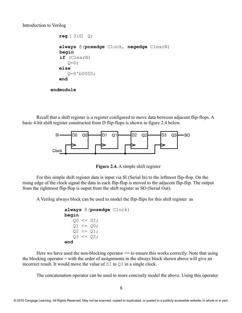
Recall that a shift register is a register configured to move data between adjacent flip-flops. A basic 4-bit shift register constructed from D flip-flops is shown in figure 2.4 below.
Figure 2.4. A simple shift register
For this simple shift register data is input via SI (Serial In) to the leftmost flip-flop. On the rising edge of the clock signal the data in each flip-flop is moved to the adjacent flip-flip. The output from the rightmost flip-flop is ouput from the shift register as SO (Serial Out).
A Verilog always block can be used to model the flip-flips for this shift register as
always @(posedge Clock)begin Q0 <= SI; Q1 <= Q0; Q2 <= Q1; Q3 <= Q2;end
Here we have used the non-blocking operator <= to ensure this works correctly. Note that using the blocking operator = with the order of assignments in the always block shown above will give an incorrect result. It would move the value of SI to Q3 in a single clock.
The concatenation operator can be used to more concisely model the above. Using this operator
8
© 2015 Cengage Learning. All Rights Reserved. May not be scanned, copied or duplicated, or posted to a publicly accessible website, in whole or in part.
Introduction to Verilog
we can rewrite the previous code as
always @(posedge Clock)begin {Q3,Q2,Q1,Q0} <= {Q2,Q1,Q0,SI};end
Instead of using separate scalar variables for each flip-flop output it is usually more convenient to use a single vector to model the flip-flops, for this 4-bit shift register we can do this with the following
reg [3:0] Q;always @(posedge Clock)begin Q <= {Q[2:0],SI};end
Here the inputs of the three rightmost flip-flops in figure 2.4 are concatenated with the serial input to the leftmost flip-flop. On the rising edge of the clock these are moved to the outputs of the four flip-flops.
A complete Verilog module for the simple shift register, using this last form of the always block, is then
module SimpleShiftRegister (SO, SI, Clock);
output SO; // serial output datainput SI; // serial input datainput Clock;
reg [3:0] Q;
always @(posedge Clock)begin Q <= {Q[2:0],SI};end
assign SO = Q[3];
endmodule
An continuous assignment statement is used to identify net SO as variable Q[3].
The logic circuit of a shift register with parallel input and output is shown in figure 2.5.
9
© 2015 Cengage Learning. All Rights Reserved. May not be scanned, copied or duplicated, or posted to a publicly accessible website, in whole or in part.

Introduction to Verilog
Figure 2.5. Shift register with parallel input and output
In addition to the serial output, SO, the outputs Q0, Q1, Q2, and Q3 of the individual flip-flops are available. In addition, a multiplexer at the input to each flip-flop selects the input source. If Load is “0” then input of each flip-flop is the output of the adjacent flip-flip or, in the case of the leftmost flip-flop, SI. In this case the circuit functions as the previous shift register. If Load is “1” then the inputs to the flip-flops are the four data inputs, D0, D1, D2, and D3.
The Verilog code for the simple shift register is easily modified. An additional 4-bit input vector D, 4-bit output vector Q, and the Load signal can be added to port list. Since the Load signal is common to all four flip-flops we can use a single if-else statement, controlled by the Load signal, in the always block to model it. The Verilog module for this parallel input and output shift register is then
module ParallelShiftRegister (SO,Q,SI,D,Load,Clock);
output SO; // serial output dataoutput [3:0] Q; // parallel output datainput SI; // serial input datainput [3:0] D; // parallel input datainput Load; // mode controlinput Clock;
reg [3:0] Q;
always @(posedge Clock)begin if(Load) Q <= D; else Q <= {Q[2:0],SI};end
assign SO = Q[3];
endmodule
10
© 2015 Cengage Learning. All Rights Reserved. May not be scanned, copied or duplicated, or posted to a publicly accessible website, in whole or in part.
Introduction to Verilog
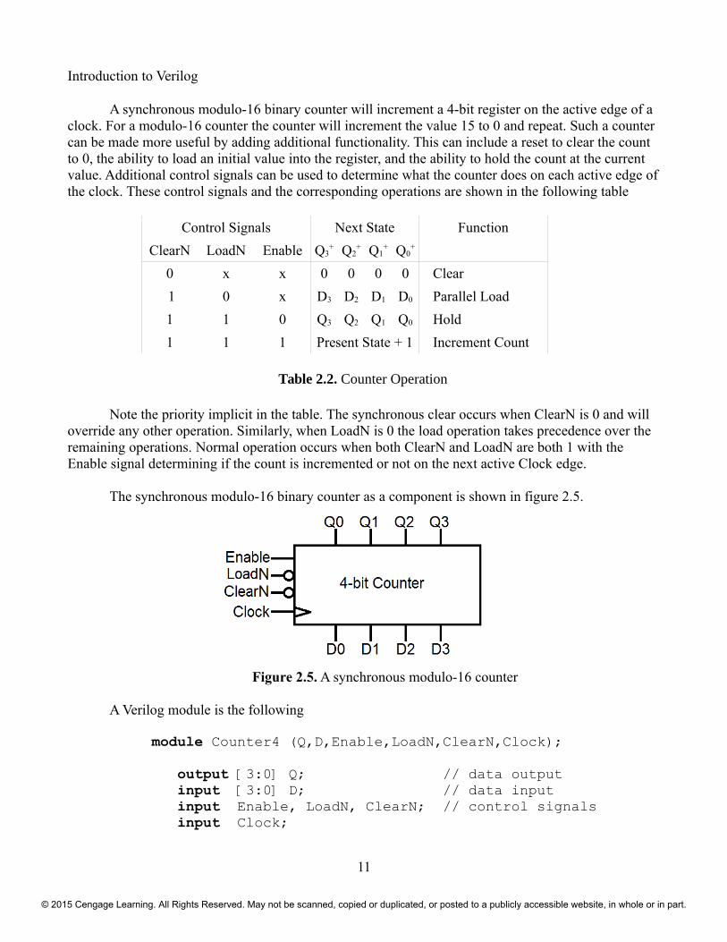
A synchronous modulo-16 binary counter will increment a 4-bit register on the active edge of a clock. For a modulo-16 counter the counter will increment the value 15 to 0 and repeat. Such a counter can be made more useful by adding additional functionality. This can include a reset to clear the count to 0, the ability to load an initial value into the register, and the ability to hold the count at the current value. Additional control signals can be used to determine what the counter does on each active edge of the clock. These control signals and the corresponding operations are shown in the following table
Control Signals Next State Function
ClearN LoadN Enable Q3+ Q2
+ Q1+ Q0
+
0 x x 0 0 0 0 Clear
1 0 x D3 D2 D1 D0 Parallel Load
1 1 0 Q3 Q2 Q1 Q0 Hold
1 1 1 Present State + 1 Increment Count
Table 2.2. Counter Operation
Note the priority implicit in the table. The synchronous clear occurs when ClearN is 0 and will override any other operation. Similarly, when LoadN is 0 the load operation takes precedence over the remaining operations. Normal operation occurs when both ClearN and LoadN are both 1 with the Enable signal determining if the count is incremented or not on the next active Clock edge.
The synchronous modulo-16 binary counter as a component is shown in figure 2.5.
Figure 2.5. A synchronous modulo-16 counter
A Verilog module is the following
module Counter4 (Q,D,Enable,LoadN,ClearN,Clock);
output [3:0] Q; // data output input [3:0] D; // data input input Enable, LoadN, ClearN; // control signals input Clock;
11
© 2015 Cengage Learning. All Rights Reserved. May not be scanned, copied or duplicated, or posted to a publicly accessible website, in whole or in part.
Introduction to Verilog
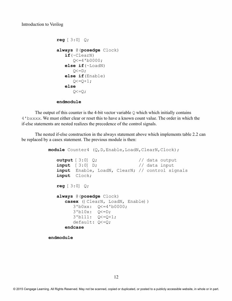
reg [3:0] Q;
always @(posedge Clock) if(~ClearN) Q<=4'b0000; else if(~LoadN) Q<=D; else if(Enable) Q<=Q+1; else Q<=Q;
endmodule
The output of this counter is the 4-bit vector variable Q which which initially contains 4'bxxxx. We must either clear or reset this to have a known count value. The order in which the if-else statements are nested realizes the precedence of the control signals.
The nested if-else construction in the always statement above which implements table 2.2 can be replaced by a casex statement. The previous module is then:
module Counter4 (Q,D,Enable,LoadN,ClearN,Clock);
output [3:0] Q; // data output input [3:0] D; // data input input Enable, LoadN, ClearN; // control signals input Clock;
reg [3:0] Q;
always @(posedge Clock) casex ({ClearN, LoadN, Enable}) 3'b0xx: Q<=4'b0000; 3'b10x: Q<=D; 3'b111: Q<=Q+1; default: Q<=Q; endcase
endmodule
12
© 2015 Cengage Learning. All Rights Reserved. May not be scanned, copied or duplicated, or posted to a publicly accessible website, in whole or in part.
Introduction to Verilog
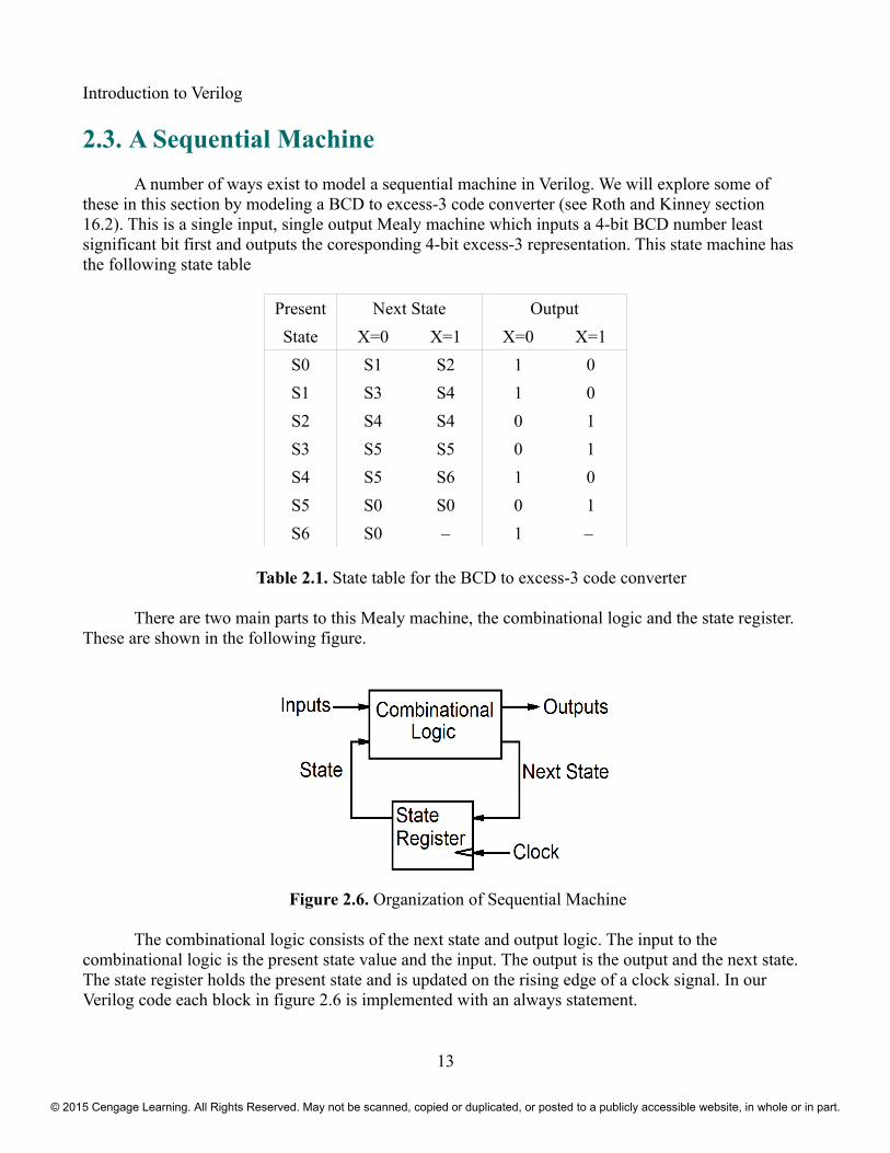
2.3. A Sequential Machine
A number of ways exist to model a sequential machine in Verilog. We will explore some of these in this section by modeling a BCD to excess-3 code converter (see Roth and Kinney section 16.2). This is a single input, single output Mealy machine which inputs a 4-bit BCD number least significant bit first and outputs the coresponding 4-bit excess-3 representation. This state machine has the following state table
Present Next State Output
State X=0 X=1 X=0 X=1
S0 S1 S2 1 0
S1 S3 S4 1 0
S2 S4 S4 0 1
S3 S5 S5 0 1
S4 S5 S6 1 0
S5 S0 S0 0 1
S6 S0 – 1 –
Table 2.1. State table for the BCD to excess-3 code converter
There are two main parts to this Mealy machine, the combinational logic and the state register. These are shown in the following figure.
Figure 2.6. Organization of Sequential Machine
The combinational logic consists of the next state and output logic. The input to the combinational logic is the present state value and the input. The output is the output and the next state. The state register holds the present state and is updated on the rising edge of a clock signal. In our Verilog code each block in figure 2.6 is implemented with an always statement.
13
© 2015 Cengage Learning. All Rights Reserved. May not be scanned, copied or duplicated, or posted to a publicly accessible website, in whole or in part.
Introduction to Verilog
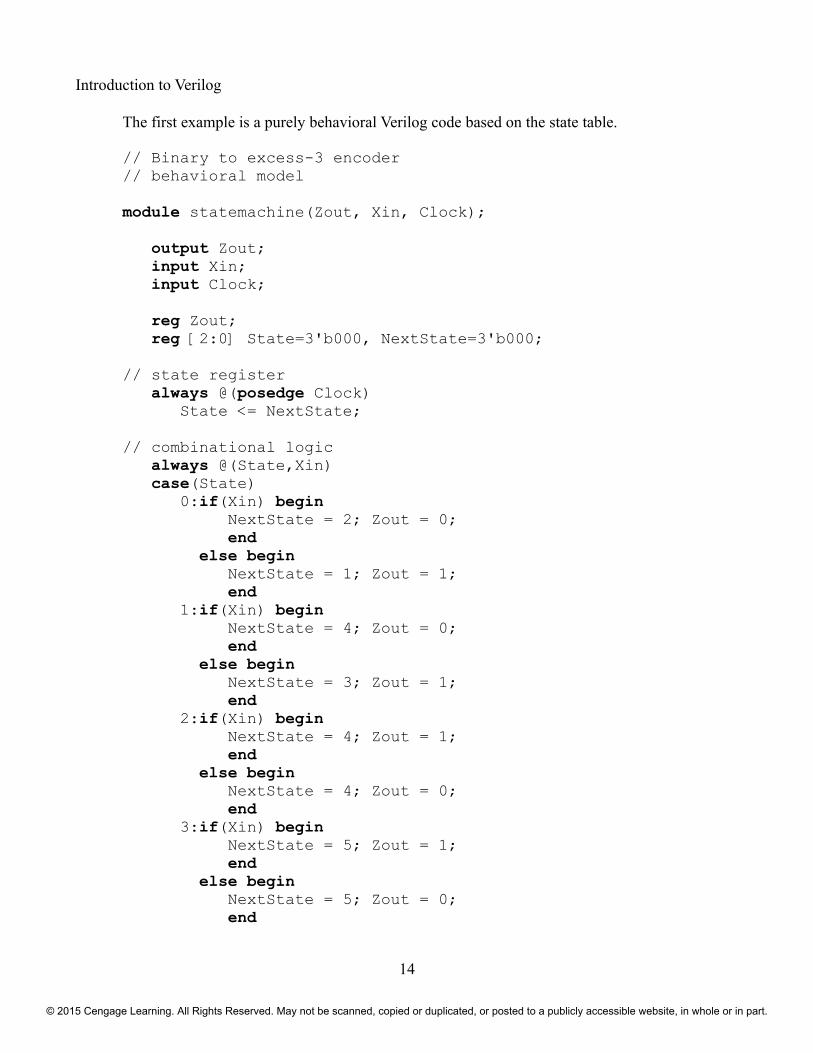
The first example is a purely behavioral Verilog code based on the state table.
// Binary to excess-3 encoder // behavioral model
module statemachine(Zout, Xin, Clock);
output Zout; input Xin; input Clock;
reg Zout; reg [2:0] State=3'b000, NextState=3'b000;
// state register always @(posedge Clock) State <= NextState;
// combinational logic always @(State,Xin) case(State) 0:if(Xin) begin NextState = 2; Zout = 0; end else begin NextState = 1; Zout = 1; end 1:if(Xin) begin NextState = 4; Zout = 0; end else begin NextState = 3; Zout = 1; end 2:if(Xin) begin NextState = 4; Zout = 1; end else begin NextState = 4; Zout = 0; end 3:if(Xin) begin NextState = 5; Zout = 1; end else begin NextState = 5; Zout = 0; end
14
© 2015 Cengage Learning. All Rights Reserved. May not be scanned, copied or duplicated, or posted to a publicly accessible website, in whole or in part.
Introduction to Verilog
4:if(Xin) begin NextState = 6; Zout = 0; end else begin NextState = 5; Zout = 1; end 5:if(Xin) begin NextState = 0; Zout = 1; end else begin NextState = 0; Zout = 0; end 6:begin NextState = 0; Zout = 1; end default: begin NextState = 4'bx; Zout = 1'bx; end endcase
endmodule
This code is based on figure 2.6 with the first always block corresponding to the state register and the second always block corresponding to the combinational logic. The action in the always block modeling the combinational logic corresponds to the state table. Note that we have used Xin and Zout as the input and output to avoid any confusion with the Verilog values X and Z.
A test bench for this state machine is the following:
// Test Bench for the statemachine `include "statemachine_b.v"
module statemachine_test;
reg Xin,Clock=0; wire Zout;
// instantiate the binary to excess-3 state machine statemachine SM(Zout,Xin,Clock);
// generate test signals initial begin Xin = 0; // begin 1010
15
© 2015 Cengage Learning. All Rights Reserved. May not be scanned, copied or duplicated, or posted to a publicly accessible website, in whole or in part.
Introduction to Verilog
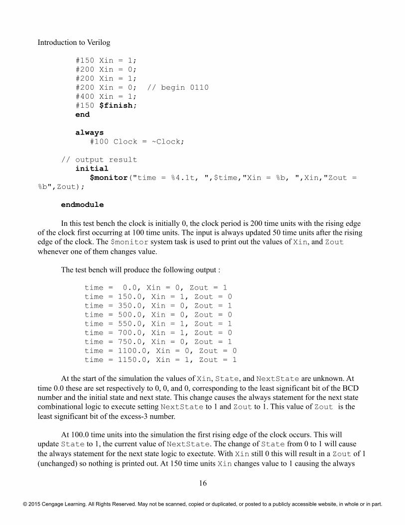
#150 Xin = 1; #200 Xin = 0; #200 Xin = 1; #200 Xin = 0; // begin 0110 #400 Xin = 1; #150 $finish; end
always #100 Clock = ~Clock;
// output result initial $monitor("time = %4.1t, ",$time,"Xin = %b, ",Xin,"Zout =
%b",Zout);
endmodule
In this test bench the clock is initially 0, the clock period is 200 time units with the rising edge of the clock first occurring at 100 time units. The input is always updated 50 time units after the rising edge of the clock. The $monitor system task is used to print out the values of Xin, and Zout whenever one of them changes value.
The test bench will produce the following output :
time = 0.0, Xin = 0, Zout = 1 time = 150.0, Xin = 1, Zout = 0 time = 350.0, Xin = 0, Zout = 1 time = 500.0, Xin = 0, Zout = 0 time = 550.0, Xin = 1, Zout = 1 time = 700.0, Xin = 1, Zout = 0 time = 750.0, Xin = 0, Zout = 1 time = 1100.0, Xin = 0, Zout = 0 time = 1150.0, Xin = 1, Zout = 1
At the start of the simulation the values of Xin, State, and NextState are unknown. At time 0.0 these are set respectively to 0, 0, and 0, corresponding to the least significant bit of the BCD number and the initial state and next state. This change causes the always statement for the next state combinational logic to execute setting NextState to 1 and Zout to 1. This value of Zout is the least significant bit of the excess-3 number.
At 100.0 time units into the simulation the first rising edge of the clock occurs. This will update State to 1, the current value of NextState. The change of State from 0 to 1 will cause the always statement for the next state logic to exectute. With Xin still 0 this will result in a Zout of 1 (unchanged) so nothing is printed out. At 150 time units Xin changes value to 1 causing the always
16
© 2015 Cengage Learning. All Rights Reserved. May not be scanned, copied or duplicated, or posted to a publicly accessible website, in whole or in part.
Introduction to Verilog
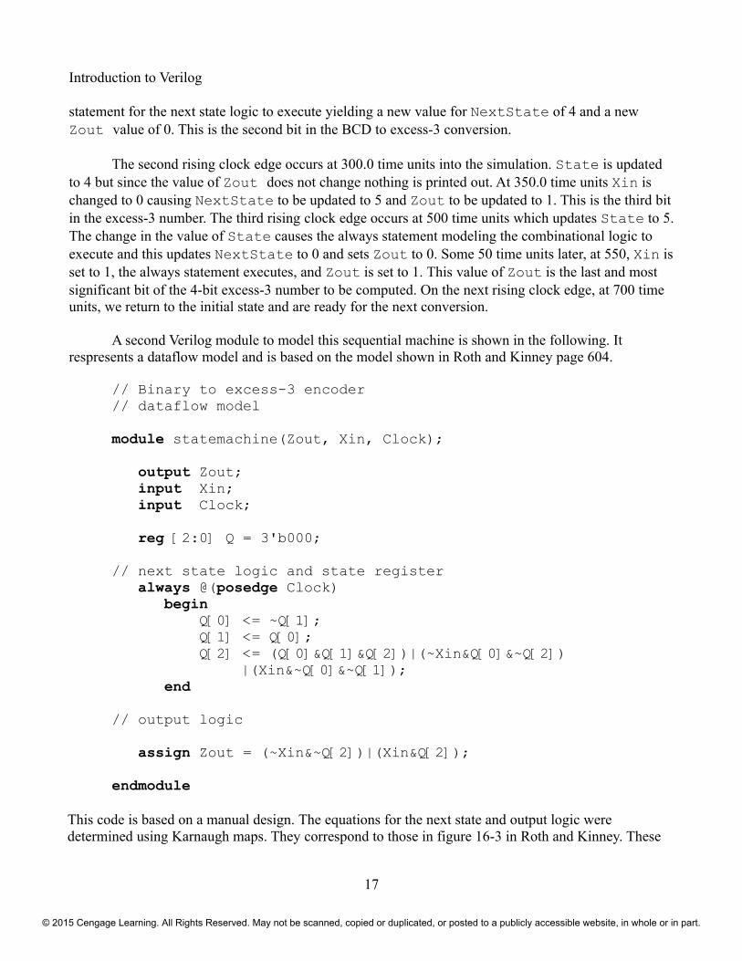
statement for the next state logic to execute yielding a new value for NextState of 4 and a new Zout value of 0. This is the second bit in the BCD to excess-3 conversion.
The second rising clock edge occurs at 300.0 time units into the simulation. State is updated to 4 but since the value of Zout does not change nothing is printed out. At 350.0 time units Xin is changed to 0 causing NextState to be updated to 5 and Zout to be updated to 1. This is the third bit in the excess-3 number. The third rising clock edge occurs at 500 time units which updates State to 5. The change in the value of State causes the always statement modeling the combinational logic to execute and this updates NextState to 0 and sets Zout to 0. Some 50 time units later, at 550, Xin is set to 1, the always statement executes, and Zout is set to 1. This value of Zout is the last and most significant bit of the 4-bit excess-3 number to be computed. On the next rising clock edge, at 700 time units, we return to the initial state and are ready for the next conversion.
A second Verilog module to model this sequential machine is shown in the following. It respresents a dataflow model and is based on the model shown in Roth and Kinney page 604.
// Binary to excess-3 encoder // dataflow model
module statemachine(Zout, Xin, Clock);
output Zout; input Xin; input Clock;
reg [2:0] Q = 3'b000;
// next state logic and state register always @(posedge Clock) begin Q[0] <= ~Q[1]; Q[1] <= Q[0]; Q[2] <= (Q[0]&Q[1]&Q[2])|(~Xin&Q[0]&~Q[2])
|(Xin&~Q[0]&~Q[1]); end
// output logic
assign Zout = (~Xin&~Q[2])|(Xin&Q[2]);
endmodule
This code is based on a manual design. The equations for the next state and output logic were determined using Karnaugh maps. They correspond to those in figure 16-3 in Roth and Kinney. These
17
© 2015 Cengage Learning. All Rights Reserved. May not be scanned, copied or duplicated, or posted to a publicly accessible website, in whole or in part.
Introduction to Verilog
were then implemented directly with the always block modeling the next state logic and the continuous assignment statement implementing the output logic. The state register is implicit in the next-state equations.
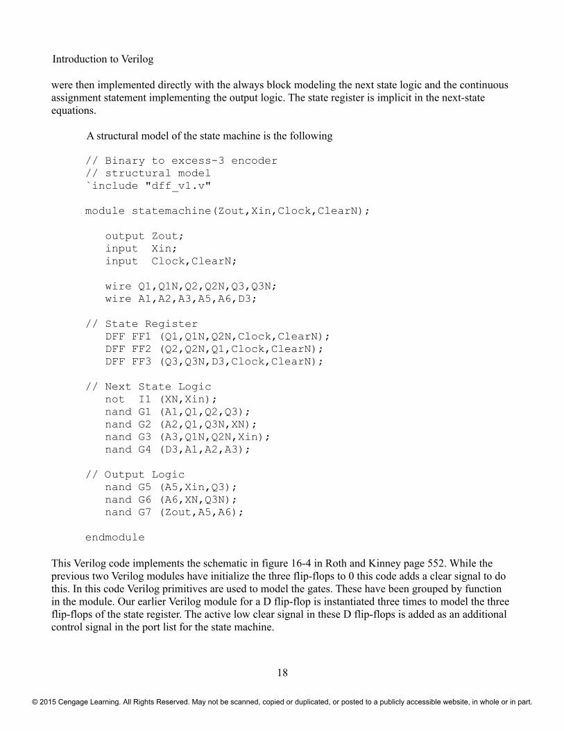
A structural model of the state machine is the following
// Binary to excess-3 encoder // structural model `include "dff_v1.v"
module statemachine(Zout,Xin,Clock,ClearN);
output Zout; input Xin; input Clock,ClearN;
wire Q1,Q1N,Q2,Q2N,Q3,Q3N; wire A1,A2,A3,A5,A6,D3;
// State Register DFF FF1 (Q1,Q1N,Q2N,Clock,ClearN); DFF FF2 (Q2,Q2N,Q1,Clock,ClearN); DFF FF3 (Q3,Q3N,D3,Clock,ClearN);
// Next State Logic not I1 (XN,Xin); nand G1 (A1,Q1,Q2,Q3); nand G2 (A2,Q1,Q3N,XN); nand G3 (A3,Q1N,Q2N,Xin); nand G4 (D3,A1,A2,A3);
// Output Logic nand G5 (A5,Xin,Q3); nand G6 (A6,XN,Q3N); nand G7 (Zout,A5,A6);
endmodule
This Verilog code implements the schematic in figure 16-4 in Roth and Kinney page 552. While the previous two Verilog modules have initialize the three flip-flops to 0 this code adds a clear signal to do this. In this code Verilog primitives are used to model the gates. These have been grouped by function in the module. Our earlier Verilog module for a D flip-flop is instantiated three times to model the three flip-flops of the state register. The active low clear signal in these D flip-flops is added as an additional control signal in the port list for the state machine.
18
© 2015 Cengage Learning. All Rights Reserved. May not be scanned, copied or duplicated, or posted to a publicly accessible website, in whole or in part.
Introduction to Verilog
2.4. Verilog for Synthesis
Verilog is widely used in logic synthesis. Synthesis involves the translation of Verilog code to a netlist with specifies the components and interconnections needed to realize a digital system. The use of Verilog, and other HDLs such as VHDL, allow for the design of large, complex, digital systems. Traditional tools would be completely inadequate in this regard. Verilog simplifies debugging, increases productivity, and allows the exploration of design tradeoffs and technology independent designs.
Verilog was originally developed to support the simulation of digital systems. Synthesis however targets hardware and only uses a subset of the Verilog HDL. When compiling for synthesis many Verilog statements are ignored or produce errors. Verilog code written for synthesis is typically at the Register Transfer Level (RTL). RTL code is a mix of behavioral and dataflow modeling.
When writing Verilog code for synthesis you should follow two general guidelines:
• Recognize your code represents hardware.
Code with the understanding that the system will be implemented in hardware. The Verilog should describe the hardware. This will usually ensure the synthesis goes smoothly.
• Work at the RTL level.
Verilog tools that synthesize hardware are designed to optimize RTL code.
For an FPGA the coding style will affect the implementation. The hardware which realizes the digital system for an FPGA consists of mutiplexers, flip-flops, LUTs, and Block RAM. Coding style for synthesis when the target is an ASIC is different. For a ASIC the hardware resources used in the design are cell gate and flip-flop libraries. The coding style used for one technology is usually not appropriate for another technology and may result in poor implementations. In the following we will look at synthesis for an FPGA and the associated coding style.
Code written for simulation may not be appropriate for synthesis. Only a subset of Verilog constructs are used in synthesis. System tasks and most compiler directives are ignored. Verilog delays are ignored. You need to be careful as delays used in a simulation may differ from delays when synthesizing to actual hardware. Declaring a real variable in code will generate an error during synthesis. Moreover, synthesis tools may reserve certain variable names. For example, Xilinx FPGAs have dedicated pins names CLK and INIT.
Combinational logic can be synthesized from primitive gates, continuous assignments, or always blocks. To describe combinational logic at the RTL level use an always block. All signals used in the always block should be explicitly assigned values every time an always block executes. If a
19
© 2015 Cengage Learning. All Rights Reserved. May not be scanned, copied or duplicated, or posted to a publicly accessible website, in whole or in part.
Introduction to Verilog
signal is not explicitly assigned a value each time, the synthesis tool will add a latch to hold the previous value. To avoid creating such latches all branches of an if-else or case statement must be specified. Nested if-else statements should be used with care as they can result in priority logic when synthesized. The case statement should be used to avoid non-prioritized multiway branches.
Sequential logic will infer flip-flops when the sensitivity list indicates the block is executed on the active edge of a clock signal. FPGAs may have dedicated reset lines.
When coding you should use blocking assignments for combinational logic and non-blocking assignments for edge-sensitive sequential logic. Blocking and non-blocking assignments should not be used in the same always block.
Synthesis tools for FPGAs can recognize FSMs from Verilog HDL code. When a FSM is recognized the synthesis tool will attempt to optimize the implementation with respect to speed or area. For an FPGA the default method for implementing an FSM is generally one-hot which can efficiently exploit the resources on an FPGA.
20
© 2015 Cengage Learning. All Rights Reserved. May not be scanned, copied or duplicated, or posted to a publicly accessible website, in whole or in part.
Introduction to Verilog
References
IEEE Standard for Verilog Hardware Description Language, IEEE Std 1364 – 2005, IEEE Computer Society, 2006
S. Palnitkar, Verilog HDL: A Guide to Digital Design and Synthesis, 2nd Edition, Prentice-Hall, 2003
C. H. Roth, and L. L. Kinney, Fundamentals of Logic Design, 7th Edition, Cengage Learning, 2013.
S. Sutherland, S. Davidmann, and P. Flake, SystemVerilog for Design: A Guide to Using SystemVerilog for Hardware Design and Modeling, 2nd Edition, Springer, 2006
S. Sutherland, Verilog is Not Called Verilog Anymore! The Merging of the Verilog and SystemVerilog IEEE Standards, Sutherland HDL, Inc. 25 February 2008
D. Thomas and P. Moorby, The Verilog Hardware Description Language, 5th Edition, Springer 2008
Xilinx, Synthesis and Simulation Design Guide, ug262 9 (v14.4) December 12, 2012
21
© 2015 Cengage Learning. All Rights Reserved. May not be scanned, copied or duplicated, or posted to a publicly accessible website, in whole or in part.