20-bit, 1-msps isolator optimized data acquisition ... electronics that support and interface with...
TRANSCRIPT

Input Frequency(kHz)
SN
R(d
Bc)
1 10 10070
75
80
85
90
95
100
105
110
D001
CONVST via ISO784xCONVST via ISO734xADS8900B Spec
ISOLATOR
PHI Connector
I2C
#CS
SCLK
SDO
RCLK
SDI(0 ± 3)
CONVSTCONVST_ISO
12-V DC
5.5 V
3.3 V
5.5 V3.3V_ISO
5V_ISO
1.8V_ISO
CONVST
#CS
SCLK
SDI
SDO 0 - 3
(READY/CLK)RVS
20-Bit1-MSPS
SAR ADC
SMA Connector
VIN+
VIN-
EEPROM
`
IN+
IN-
+
5V_ISO
3.3V_ISO
3.3 V
1.8V_ISO
AVDD DVDD
DVDD_ISO
VREF
_
_
+
Vocm
Vocm
TPS709XX /TPS7A4700
LDO
SN6501Pushpull
driver
LMZ14203TZDC-DC Buck
TPS7A4700LDO
SN74AVC4T245VOLTAGE
LEVELTRANSLATOR
ISO78XX /ISO1541
THS4551
OPA376
ADS8900B
ISO_GND GND
ISO734X
REF5050Reference
5 V
Optional jitter reduce block on ADC side
Optional jitter block to reduce host added jitter on CONVST
#CS_ISO
SCLK_ISO
SDI_ISO
SDO(0 ± 3)_ISO
RVS_ISO
Copyright © 2017, Texas Instruments Incorporated
OPTIONAL
1TIDUCM8A–December 2016–Revised January 2017Submit Documentation Feedback
Copyright © 2016–2017, Texas Instruments Incorporated
20-Bit, 1-MSPS Isolator Optimized Data Acquisition Reference DesignMaximizing SNR and Sample Rate
TI Designs20-Bit, 1-MSPS Isolator Optimized Data AcquisitionReference Design Maximizing SNR and Sample Rate
DescriptionThe TIDA-01037 is a 20-bit, 1-MSPS isolated analoginput data acquisition (DAQ) reference design thatuses two different isolator devices to maximize signalchain SNR and sample rate performance. For signalsrequiring low jitter, such as ADC sampling clocks, TI’sISO73xx family of low jitter devices are used whereasTI’s high-speed ISO78xx family of devices are used tomaximize data sample rate. By combining these twoisolator solutions, high-frequency performance issignificantly improved by minimizing sample clock jitteracross the isolation boundary, and data throughput isimproved by maximizing isolator signaling rate.Additional improvements are realized by using TI’sadvanced ADC multiSPI™ and source-synchronousfeatures. Finally, all key design theories are describedand measured results presented in Section 4.2.
Resources
TIDA-01037 Design FolderADS8900B, REF5050,THS4551 Product Folder
ISO7840, ISO7842, ISO1541,ISO7340 Product Folder
SN6501, LMZ14203,TPS7A4700, Product Folder
TPS70918, OPA376,LMK61E2 Product Folder
SN65LVDS4RSET,SN74AUP1G80 Product Folder
SN74AHC1G04 Product FolderADS8900B EVM-PDK Associated Design
ASK Our E2E Experts
Features• Differential Input, Isolated, 20-Bit, 1-MSPS, DAQ
Reference Design• Optimized Isolator Solution for Input Signals up to
100 kHz• Additional Jitter Mitigation Circuitry Not Required• Demonstrates Low SPI Clock Rates With TI’s
Innovative multiSPI™ and Source-SynchronousMode ADC Digital Interfaces
• Provides Capability to Evaluate System SNRPerformance Due to Sample Clock Jitter
• Includes Theory, Calculations, ComponentSelection, PCB Design and Measurement Results
Applications• Data Acquisition (DAQ)• Lab Instrumentation and Field Instrumentation• Design Validation and Verification• Remote Process Monitoring and Control
Sensor
I/P protection
Amp FilterDigitizer
(A/D)
MCUor
FPGA
Control circuitD/A Digital IO
Volt or Current IO
Direct sensor interface
Optional
DAQ
Data processing
Plottingand
data logging
Host
Physical phenomena
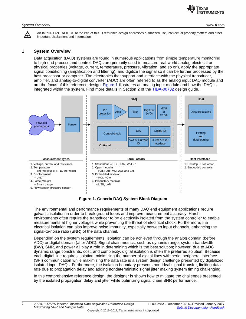
Measurement Types Form Factors Host Interfaces
1. Voltage, current and resistance2. Temperature ± Thermocouple, RTD, thermistor3. Displacement ± LVDT4. Force, Weight ± Strain gauge5. Flow sensor, pressure sensor
1. Standalone ± USB, LAN, Wi-)L2. Open modular ± PXI, PXIe, VXI, AXI, and LXI3. Embedded modular ± PCI, PCIe4. Proprietary modular ± USB, LAN
1. Desktop PC or laptop2. Embedded controller
System Overview www.ti.com
2 TIDUCM8A–December 2016–Revised January 2017Submit Documentation Feedback
Copyright © 2016–2017, Texas Instruments Incorporated
20-Bit, 1-MSPS Isolator Optimized Data Acquisition Reference DesignMaximizing SNR and Sample Rate
An IMPORTANT NOTICE at the end of this TI reference design addresses authorized use, intellectual property matters and otherimportant disclaimers and information.
1 System OverviewData acquisition (DAQ) systems are found in numerous applications from simple temperature monitoringto high-end process and control. DAQs are primarily used to measure real-world analog electrical orphysical properties (voltage, current, temperature, pressure, vibration, and so on), apply the appropriatesignal conditioning (amplification and filtering), and digitize the signal so it can be further processed by thehost processor or computer. The electronics that support and interface with the physical transducer,amplifier, and analog-to-digital converter (ADC) are often referred to as the analog input DAQ module andare the focus of this reference design. Figure 1 illustrates an analog input module and how the DAQ isintegrated within the system. Find more details in Section 2 of the TIDA-00732 design guide.
Figure 1. Generic DAQ System Block Diagram
The environmental and performance requirements of many DAQ end equipment applications requiregalvanic isolation in order to break ground loops and improve measurement accuracy. Harshenvironments often require the transducer to be electrically isolated from the system controller to enablemeasurements at higher voltages while preventing the threat of electrical shock. Furthermore, theelectrical isolation can also improve noise immunity, especially between input channels, enhancing thesignal-to-noise ratio (SNR) of the data channel.
Depending on the system requirements, isolation can be achieved through the analog domain (beforeADC) or digital domain (after ADC). Signal chain metrics, such as dynamic range, system bandwidth(BW), SNR, and power all play a role in determining which is the best solution; however, due to ADCdynamic range constraints, cost, and complexity, digital isolation is often the preferred solution. Becauseeach digital line requires isolation, minimizing the number of digital lines with serial peripheral interface(SPI) communication while maximizing the data rate is a system design challenge presented by digitalizedisolated input DAQs. Furthermore, the isolation boundary presents non-ideal signal transfer, limiting datarate due to propagation delay and adding nondeterministic signal jitter making system timing challenging.
In this comprehensive reference design, the designer is shown how to mitigate the challenges presentedby the isolated propagation delay and jitter while optimizing signal chain SNR performance.
Input protection
AmpADC driver
LPF
ADC MCU or FPGA
USB or LAN
PXI or PCI
VXI or LXI
HMI
VCOM REF
DC-DC
DC-DC
LDO
LDO
DC-DC
OSC
RAM
Isolation Barrer
LDO
LDO
LDO
LDO
12-V DC
3.3 V
2.5 V
1.8 V
1.2 V
(15 or 5 V)
(5 or 3.3 V)
(3.3 or 1.8 V)
(±15 or ±5 V)
+VCC
AVDD
DVDD
±VEE
Isolated power rail
Non-isolated power rail
Isolation Transformer
Digital Isolator
Serial or parallel
interface
Sample clock control
lines
Integrated AFE
±VEE ±VEE
+VCC +VCC
SPI or I2C
Host interface
AVDD DVDD
AVDD DVDDIN+
IN±
Gain selection
Optional
www.ti.com System Overview
3TIDUCM8A–December 2016–Revised January 2017Submit Documentation Feedback
Copyright © 2016–2017, Texas Instruments Incorporated
20-Bit, 1-MSPS Isolator Optimized Data Acquisition Reference DesignMaximizing SNR and Sample Rate
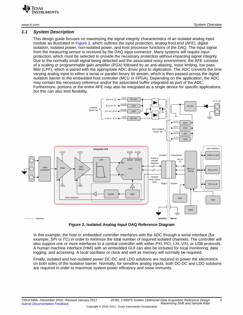
1.1 System DescriptionThis design guide focuses on maximizing the signal integrity characteristics of an isolated analog inputmodule as illustrated in Figure 2, which outlines the input protection, analog front end (AFE), digitalisolation, isolated power, non-isolated power, and host processor functions of the DAQ. The input signalfrom the measuring sensor is received by the DAQ input connector. Many systems will require inputprotection, which must be selected to provide the necessary protection without impacting signal integrity.Due to the normally small signal being detected and the associated noisy environment, the AFE consistsof a scaling or programmable gain amplifier (PGA) followed by an anti-aliasing, noise limiting, low passfilter (LPF), which is paired with the appropriate ADC driver prior to digitization. The ADC converts the timevarying analog input to either a serial or parallel binary bit stream, which is then passed across the digitalisolation barrier to the embedded host controller (MCU or FPGA). Depending on the application, the ADCmay contain the necessary reference and/or the associated buffer integrated as part of the ADC.Furthermore, portions or the entire AFE may also be integrated as a single device for specific applications,but this can also limit flexibility.
Figure 2. Isolated Analog Input DAQ Reference Diagram
In this example, the host or embedded controller interfaces with the ADC through a serial interface (forexample, SPI or I2C) in order to minimize the total number of required isolated channels. The controller willalso support one or more interfaces to a central controller with either PXI, PCI, LXI, VXI, or USB protocols.A human machine interface (HMI) with an embedded GUI can also be included for local monitoring, datalogging, and accessing. A local oscillator or clock and well as memory will normally be required.
Finally, isolated and non-isolated power DC-DC and LDO solutions are required to power the electronicson both sides of the isolation barrier. Normally, for sensitive analog inputs, both DC-DC and LDO solutionsare required in order to maximize system power efficiency and noise immunity.
System Overview www.ti.com
4 TIDUCM8A–December 2016–Revised January 2017Submit Documentation Feedback
Copyright © 2016–2017, Texas Instruments Incorporated
20-Bit, 1-MSPS Isolator Optimized Data Acquisition Reference DesignMaximizing SNR and Sample Rate
The following sections detail the timing challenges presented by the isolation barrier in terms of its effecton the ADC’s data rate and SNR performance, and the challenges of synchronizing the sample clock withthe host clock. When these performance limiting characteristics are understood, solutions using keyfeatures of TI’s high performance AFE solutions for amplifiers, ADCs, and isolation devices are highlightedalong with TI’s power solutions for both isolated and non-isolated supplies. Furthermore, a novel designfor synchronizing the ADC’s sample clock with the host clock is also demonstrated.
For more background information on DAQ challenges and solutions, see the TIDA-00732 and TIDA-00164designs.
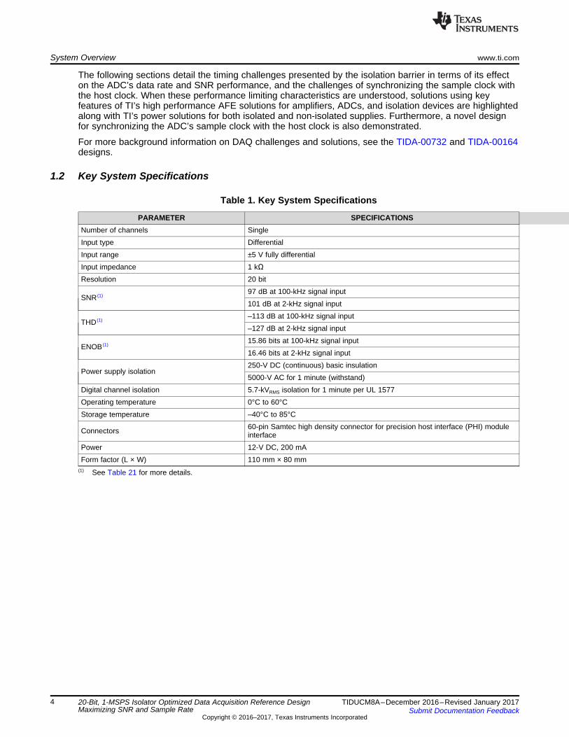
1.2 Key System Specifications
(1) See Table 21 for more details.
Table 1. Key System Specifications
PARAMETER SPECIFICATIONSNumber of channels SingleInput type DifferentialInput range ±5 V fully differentialInput impedance 1 kΩResolution 20 bit
SNR (1)97 dB at 100-kHz signal input101 dB at 2-kHz signal input
THD (1)–113 dB at 100-kHz signal input–127 dB at 2-kHz signal input
ENOB (1)15.86 bits at 100-kHz signal input16.46 bits at 2-kHz signal input
Power supply isolation250-V DC (continuous) basic insulation5000-V AC for 1 minute (withstand)
Digital channel isolation 5.7-kVRMS isolation for 1 minute per UL 1577Operating temperature 0°C to 60°CStorage temperature –40°C to 85°C
Connectors 60-pin Samtec high density connector for precision host interface (PHI) moduleinterface
Power 12-V DC, 200 mAForm factor (L × W) 110 mm × 80 mm
ISOLATOR
PHI Connector
I2C
#CS
SCLK
SDO
RCLK
SDI(0 ± 3)
CONVSTCONVST_ISO
12-V DC
5.5 V
3.3 V
5.5 V3.3V_ISO
5V_ISO
1.8V_ISO
CONVST
#CS
SCLK
SDI
SDO 0 - 3
(READY/CLK)RVS
20-Bit1-MSPS
SAR ADC
SMA Connector
VIN+
VIN-
EEPROM
`
IN+
IN-
+
5V_ISO
3.3V_ISO
3.3 V
1.8V_ISO
AVDD DVDD
DVDD_ISO
VREF
_
_
+
Vocm
Vocm
TPS709XX /TPS7A4700
LDO
SN6501Pushpull
driver
LMZ14203TZDC-DC Buck
TPS7A4700LDO
SN74AVC4T245VOLTAGE
LEVELTRANSLATOR
ISO78XX /ISO1541
THS4551
OPA376
ADS8900B
ISO_GND GND
ISO734X
REF5050Reference
5 V
Optional jitter reduce block on ADC side
Optional jitter block to reduce host added jitter on CONVST
#CS_ISO
SCLK_ISO
SDI_ISO
SDO(0 ± 3)_ISO
RVS_ISO
Copyright © 2017, Texas Instruments Incorporated
OPTIONAL
www.ti.com System Overview
5TIDUCM8A–December 2016–Revised January 2017Submit Documentation Feedback
Copyright © 2016–2017, Texas Instruments Incorporated
20-Bit, 1-MSPS Isolator Optimized Data Acquisition Reference DesignMaximizing SNR and Sample Rate
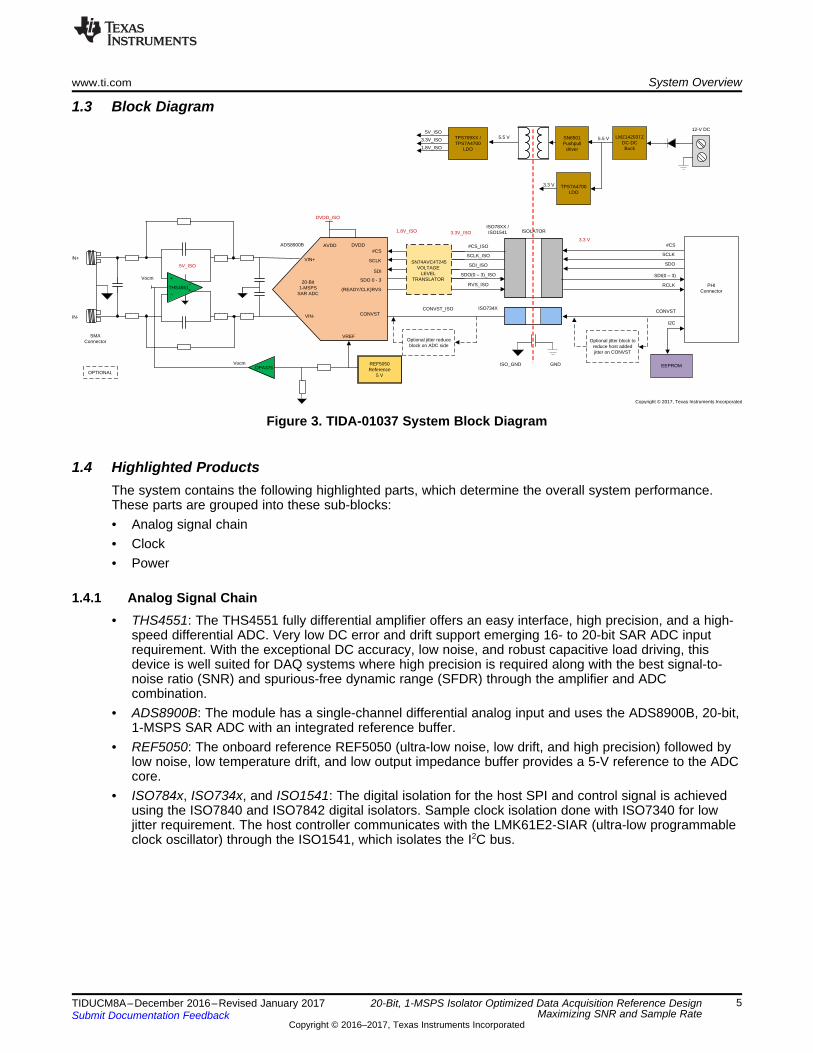
1.3 Block Diagram
Figure 3. TIDA-01037 System Block Diagram
1.4 Highlighted ProductsThe system contains the following highlighted parts, which determine the overall system performance.These parts are grouped into these sub-blocks:• Analog signal chain• Clock• Power
1.4.1 Analog Signal Chain• THS4551: The THS4551 fully differential amplifier offers an easy interface, high precision, and a high-
speed differential ADC. Very low DC error and drift support emerging 16- to 20-bit SAR ADC inputrequirement. With the exceptional DC accuracy, low noise, and robust capacitive load driving, thisdevice is well suited for DAQ systems where high precision is required along with the best signal-to-noise ratio (SNR) and spurious-free dynamic range (SFDR) through the amplifier and ADCcombination.
• ADS8900B: The module has a single-channel differential analog input and uses the ADS8900B, 20-bit,1-MSPS SAR ADC with an integrated reference buffer.
• REF5050: The onboard reference REF5050 (ultra-low noise, low drift, and high precision) followed bylow noise, low temperature drift, and low output impedance buffer provides a 5-V reference to the ADCcore.
• ISO784x, ISO734x, and ISO1541: The digital isolation for the host SPI and control signal is achievedusing the ISO7840 and ISO7842 digital isolators. Sample clock isolation done with ISO7340 for lowjitter requirement. The host controller communicates with the LMK61E2-SIAR (ultra-low programmableclock oscillator) through the ISO1541, which isolates the I2C bus.
5V_ISO
3P3V_ISO
1P8V_ISO
DC-DCLMZ14203TZ-ADJ
5.5 V
LDOTPS7A4700RGWR
3P3V
+12 VDC 5.5 V5.4 VDC OPAMP,
REFERENCED1
D2
SN6501
+
ISOLATOR,LOGIC
CLOCK,
LOGICISOLATOR
Non-isolated power supply rail Isolated power supply rail
( 5.2 V )
( 3.3 V )
( 1.8 V )
( 3.3 V )
AGND_ISOAGND
AGND AGND_ISO
T1
LDOTPS7A4700RGWR
LDOTPS70918DBVT
LDOTPS7A4700RGWR
Copyright © 2016, Texas Instruments Incorporated
System Overview www.ti.com
6 TIDUCM8A–December 2016–Revised January 2017Submit Documentation Feedback
Copyright © 2016–2017, Texas Instruments Incorporated
20-Bit, 1-MSPS Isolator Optimized Data Acquisition Reference DesignMaximizing SNR and Sample Rate
1.4.2 ClockThe LMK61E2 programmable oscillator has the following features:• Ultra-low noise, high performance (90 fs RMS jitter at > 100 MHz)• Frequency tolerance ±50 ppm• Frequency output 10 MHz to 1 GHz• I2C interface
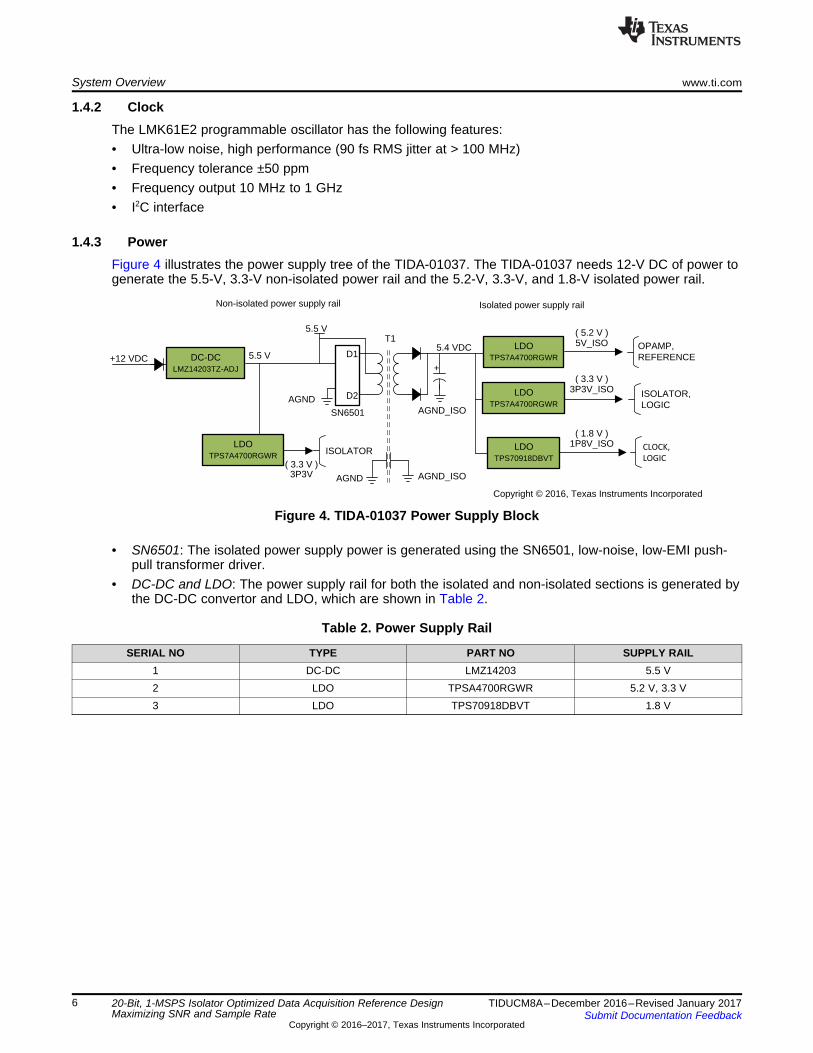
1.4.3 PowerFigure 4 illustrates the power supply tree of the TIDA-01037. The TIDA-01037 needs 12-V DC of power togenerate the 5.5-V, 3.3-V non-isolated power rail and the 5.2-V, 3.3-V, and 1.8-V isolated power rail.
Figure 4. TIDA-01037 Power Supply Block
• SN6501: The isolated power supply power is generated using the SN6501, low-noise, low-EMI push-pull transformer driver.
• DC-DC and LDO: The power supply rail for both the isolated and non-isolated sections is generated bythe DC-DC convertor and LDO, which are shown in Table 2.
Table 2. Power Supply Rail
SERIAL NO TYPE PART NO SUPPLY RAIL1 DC-DC LMZ14203 5.5 V2 LDO TPSA4700RGWR 5.2 V, 3.3 V3 LDO TPS70918DBVT 1.8 V

SS
SCLK
MOSI
MISO
D1 D2 D4 D5 D6 D7D3
D0 D1 D3 D4 D5 D6 D7D2
CPOL = 0, CPHA = 1
D0
0 1 2 3 4 5 6 7 0 1 2 3 4 5 6 7MOSI
MISO
SCLK
SPI Master SPI Slave
Shift register Shift registerCLK
www.ti.com System Design Theory
7TIDUCM8A–December 2016–Revised January 2017Submit Documentation Feedback
Copyright © 2016–2017, Texas Instruments Incorporated
20-Bit, 1-MSPS Isolator Optimized Data Acquisition Reference DesignMaximizing SNR and Sample Rate
2 System Design TheoryGalvanic isolation is commonly used by DAQ systems in order to breaks ground loops and therebyimproves measurement accuracy and safety. Isolation may be achieved within the analog domain prior tothe ADC or in the digital domain after the ADC. Prior to this publication, digital isolation was the preferredembodied solution for systems requiring medium performance (resolution < 16 bits, sampling rates < 1MSPS, and BW < 100 kHz). However, for higher resolution, higher speed solutions (> 18 bits, > 1 MSPS,and > 100 kHz), digital isolators will limit signal chain performance, dramatically reducing the DAQ’seffective number of bits (ENOB). Digital isolators present two main design challenges:1. Propagation delay in digital isolator (described in Section 2.1)2. Additive jitter due to digital isolator (described in Section 2.2)
These challenges and a detailed analysis of their impact with examples are described in the followingsections.
2.1 Isolated DAQ Signal Chain Design—Timing AnalysisIn DAQ systems, isolation in the signal chain breaks ground loops and thereby improves measurementaccuracy and safety. Isolation may be achieved within the analog domain prior to the ADC or in the digitaldomain, after the ADC. Digital isolation is preferred when higher sampling rates are required. However, fora higher resolution (> 16 bits) and higher speed (>1 MSPS), the propagation delay and jitter of the digitalisolator limits the signal chain performance for higher input signal frequencies. The propagation delayreduces the sampling rate of the signal chain. The jitter introduced by the digital isolator degrades theSNR at higher input frequencies.
This design guide describes the performance impact of propagation delay and jitter associated withisolated DAQ systems, explains the theory, calculation, and design, and presents examples.
2.1.1 Effect of Propagation Delay on Sampling RateIn a typical DAQ system, a serial peripheral interface (SPI) transfers data between the ADC and the host.Figure 5 shows a generic SPI block diagram. The host is generally the SPI master that decides thesampling rate and data transfer rate. In a typical SPI Motorola® protocol, the host sends data at risingedge and receives data on the falling edge within the same clock cycle.
Figure 5. SPI Block Diagram
Figure 6. SPI Timing Diagram
maxpd
1SCLK
2 t=
´
System Design Theory www.ti.com
8 TIDUCM8A–December 2016–Revised January 2017Submit Documentation Feedback
Copyright © 2016–2017, Texas Instruments Incorporated
20-Bit, 1-MSPS Isolator Optimized Data Acquisition Reference DesignMaximizing SNR and Sample Rate
As depicted in Figure 6, the host expects valid data before the clock falling edge. The total round-trippropagation delay should be less than half the SCLK period to avoid missing bits. Hence, the theoreticalmaximum SPI clock can be calculated as:
(1)
Equation 1 assumes that there is no change in the waveform shape. However, digital signals becomeanalog in nature as they have finite rise-fall times, which result in waveform deformities causing pulsewidth distortion (PWD) as they propagate through different digital signal chain elements. The pulse widthof the clock or the data line changes due the different threshold voltages and rise-fall times of the digitaldevices in the path.
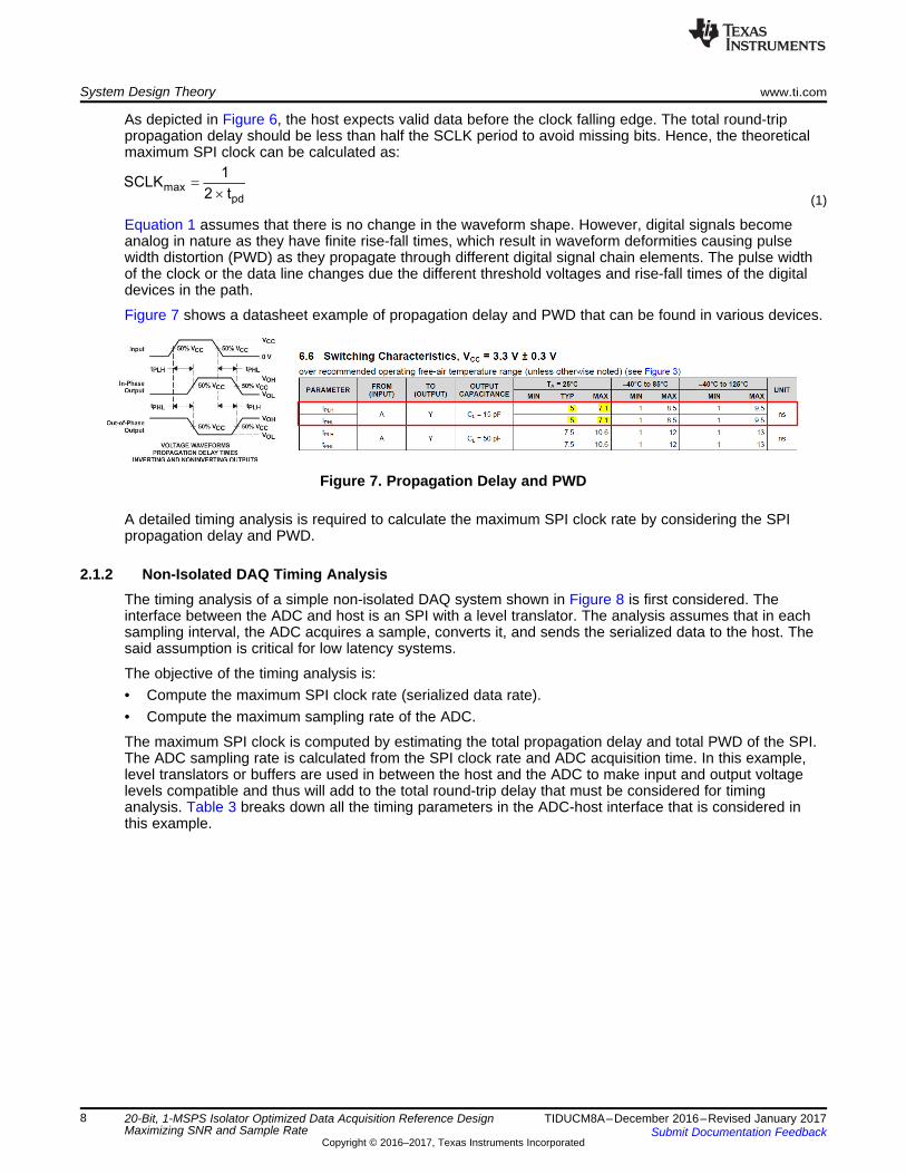
Figure 7 shows a datasheet example of propagation delay and PWD that can be found in various devices.
Figure 7. Propagation Delay and PWD
A detailed timing analysis is required to calculate the maximum SPI clock rate by considering the SPIpropagation delay and PWD.
2.1.2 Non-Isolated DAQ Timing AnalysisThe timing analysis of a simple non-isolated DAQ system shown in Figure 8 is first considered. Theinterface between the ADC and host is an SPI with a level translator. The analysis assumes that in eachsampling interval, the ADC acquires a sample, converts it, and sends the serialized data to the host. Thesaid assumption is critical for low latency systems.
The objective of the timing analysis is:• Compute the maximum SPI clock rate (serialized data rate).• Compute the maximum sampling rate of the ADC.
The maximum SPI clock is computed by estimating the total propagation delay and total PWD of the SPI.The ADC sampling rate is calculated from the SPI clock rate and ADC acquisition time. In this example,level translators or buffers are used in between the host and the ADC to make input and output voltagelevels compatible and thus will add to the total round-trip delay that must be considered for timinganalysis. Table 3 breaks down all the timing parameters in the ADC-host interface that is considered inthis example.

RTPD _ max PD _HOST _ SCLK PD _BUF ADC _ SCLK _MISO HOST _ SCLK _MISOt t 2 t t t= + ´ + +
DQ
D Q
Level Translator HostADC
SCLK_ADC
SDO-0_ADC
1.8 V 3.3 V
tADC_SCLK_MOSI
tPCB_BUF_ADC tPWD_BUF
tPD_BUF
tPCB_HOST_BUF
DQ
tHOST_SCLK_MISO
tHOST_CLK_Q
SCLK Gen
SDI_0_HOST
SCLK_HOST
Roundtripdelay path
Copyright © 2017, Texas Instruments Incorporated
www.ti.com System Design Theory
9TIDUCM8A–December 2016–Revised January 2017Submit Documentation Feedback
Copyright © 2016–2017, Texas Instruments Incorporated
20-Bit, 1-MSPS Isolator Optimized Data Acquisition Reference DesignMaximizing SNR and Sample Rate
Figure 8. Simple Non-Isolated SPI ADC-Host Interface
Table 3. Timing Parameter
PARAMETER DESCRIPTIONtSCLK_min Minimum SCLK periodtPCB_HOST_ISO PCB trace delay between host and isolatortPCB_HOST_BUF PCB trace delay between host and buffertPD_ISO Isolator propagation delaytPD_BUF Buffer or level translator propagation delaytPCB_BUF_ADC PCB trace delay between buffer and ADCtPCB_ADC_BUF PCB trace delay between ADC and buffertPCB_BUF_ISO PCB trace delay between buffer and isolatortPCB_ISO_HOST PCB trace delay between isolator and hosttSU_HOST Setup time of host MISO linetPLHmax Maximum propagation delay from low to hightPHLmin Minimum propagation delay from high to lowtPHLmax Maximum propagation delay from high to lowtPLHmin Minimum propagation delay from low to hightPWD_BUF_max Maximum pulse width distortion of buffer or level translatortSCLK_PH_min Minimum positive clock high periodtPWD_HOST_max Maximum host pulse width distortionfSCLK_max Maximum SCLK frequencytPD_HOST_SCLK Propagation delay of host SCLK at host endtADC_SCLK_MOSI ADC SCLK to MOSI output delaytHOST_SCLK_MISO Host SCLK to MISO delaytRTPD_max Maximum propagation round-trip delaytOD_BUF Buffer output delay due impedance mismatch and loading effect of receivertOD_ISO Isolator output delay due impedance mismatch and loading effect of receiver
(2)

SCLK _maxSCLK _PH
1f 48.1MHz
2 t= =
´
SCLK _PH SCLK _PH_min PWD_BUF _max PWD_HOST _maxt t t t= + +
PWD_BUF _maxt 4.4 ns=
( )PWD_BUF _maxt 4.5 0.1 , 4.5 0.1= - -
( )PWD _BUF _ max PLHmax PHLmin PHLmax PLHmint max t t , t t= - -
( )max max_ adc _ limited, max_ rtpd _ limitedSCLK min SCLK SCLK=
System Design Theory www.ti.com
10 TIDUCM8A–December 2016–Revised January 2017Submit Documentation Feedback
Copyright © 2016–2017, Texas Instruments Incorporated
20-Bit, 1-MSPS Isolator Optimized Data Acquisition Reference DesignMaximizing SNR and Sample Rate
2.1.2.1 Determining Maximum SPI Clock (SCLK)In low latency system, the converted data should be made available to host system with minimum delay. Ahigher SCLK results in lower latency. The SPI clock should be computed for two cases:1. SPI clock limited by ADC2. SPI clock limited by round-trip delay
The minimum of these cases is the maximum SPI clock. Section 2.1.2.2 details the procedure to find themaximum SPI clock for a non-isolated SPI example.
(3)
2.1.2.2 SPI Clock Limited by ADCThe maximum SPI SCLK is same as ADC_SCLK. However, the SPI SCLK duty cycle is affected by thePWD of the various digital devices it passes through. As a result, the maximum SPI SCLK limited by theADC and digital device in the path is computed from tSCLK_ADC_max and tPWD_BUF_max.
The system shown in Figure 8 is used as an example with individual devices as listed in Table 4.
Table 4. Devices Used in Non-Isolated and Isolated Interface Examples
SERIAL NO DESCRIPTION DEVICE1 ADC ADS8900B2 LEVEL TRANSLATOR 74AVC4T2453 ISOLATOR ISO78XX5 Flip-flop SN74AUP1G804 PCB TYPE FR4 - 4layer
Step 1: Estimating PWD of the BufferTo find the PWD for the buffer 74AVC4T245, the max and min values of tPLH and tPHL are taken from the74AVC4T245 datasheet.
(4)
Step 2: Calculating Maximum ADC Clock
(5)
Table 5. Non-Isolated Interface Timing Parameters
PARAMETER DELAY (ns) REMARKtPWD_HOST_max 0 —
tPWD_BUF_max (tPWD_BUF + tOD_BUF ) 4.40 No buffer or level translator in the TIDA-01037 round-trippath
tSCLK_PH_min (0.45 × tADC_CLK_min) 5.99 —tSCLK_PH 10.39 —
(6)
The maximum SCLK frequency supported by the ADC is 48 MHz.
tCONVST_CYCLE
tSCLK
CONVST
SCLK
tCONV
tACQ or tSPIDATA transfer
SCS
D0 D1 D20
td5
D0 D1 D20
td6 20 × tSCLK
Copyright © 2017, Texas Instruments Incorporated
CONVST _CYCLE _min CONV SCLK _mint t N t= + ´
SCLK _max 9
1t 30 MHz
2 16.7 10-= @
´ ´
SCLK _min RTPD_maxt 2 t³ ´
RTPD _ max
RTPD _ max
t 0 ns 2 4.5 ns 6.5 ns 1.2 ns
t 16.7 ns
= + ´ + +
=
RTPD_max PD_HOST _SCLK PD_BUF ADC_SCLK _MISO HOST _SCLK _MISOt t 2 t t t= + ´ + +
www.ti.com System Design Theory
11TIDUCM8A–December 2016–Revised January 2017Submit Documentation Feedback
Copyright © 2016–2017, Texas Instruments Incorporated
20-Bit, 1-MSPS Isolator Optimized Data Acquisition Reference DesignMaximizing SNR and Sample Rate
2.1.2.3 SCLK Limited by Round-Trip Delay and Host SPIThe SCLK limited by round-trip delay is computed by finding the total propagation delay of the path thatstarts from the host MOSI and back to the host MISO through the ADC, which is marked as "round-trip" inFigure 8.
(7)
(8)
(9)
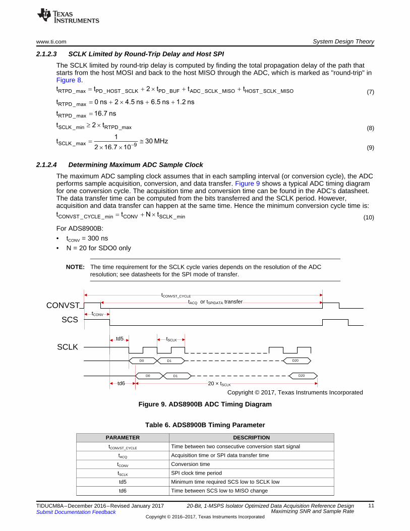
2.1.2.4 Determining Maximum ADC Sample ClockThe maximum ADC sampling clock assumes that in each sampling interval (or conversion cycle), the ADCperforms sample acquisition, conversion, and data transfer. Figure 9 shows a typical ADC timing diagramfor one conversion cycle. The acquisition time and conversion time can be found in the ADC’s datasheet.The data transfer time can be computed from the bits transferred and the SCLK period. However,acquisition and data transfer can happen at the same time. Hence the minimum conversion cycle time is:
(10)
For ADS8900B:• tCONV = 300 ns• N = 20 for SDO0 only
NOTE: The time requirement for the SCLK cycle varies depends on the resolution of the ADCresolution; see datasheets for the SPI mode of transfer.
Figure 9. ADS8900B ADC Timing Diagram
Table 6. ADS8900B Timing Parameter
PARAMETER DESCRIPTIONtCONVST_CYCLE Time between two consecutive conversion start signal
tACQ Acquisition time or SPI data transfer timetCONV Conversion timetSCLK SPI clock time periodtd5 Minimum time required SCS low to SCLK lowtd6 Time between SCS low to MISO change

DQ
D Q
Level Translator
Isolator HostADC
SCLK_ADC
SDO-0_ADC
1.8 V 3.3 V 3.3 V
tADC_SCLK_MOSI
tPCB_BUF_ADC
tPWD_BUF_ADC
tPD_BUF
tPWD_BUF
tPCB_ISO_BUF
tPWD_ISO_BUF
tPD_ISO
tPWD_ISO
tPCB_ISO_HOST
tPWD_ISO_HOST
DQ
tHOST_SCLK_MISO
tHOST_CLK_Q
SCLK Gen
SDI_0_HOST
SCLK_HOST
SDI_0_HOST
Roundtripdelay path
Copyright © 2017, Texas Instruments Incorporated
ADC_SAMPLECLK _max
CONVSCLK _max
1f
1N t
f
æ öç ÷ç ÷
= ç ÷æ öç ÷´ +ç ÷ç ÷ç ÷è øè ø
System Design Theory www.ti.com
12 TIDUCM8A–December 2016–Revised January 2017Submit Documentation Feedback
Copyright © 2016–2017, Texas Instruments Incorporated
20-Bit, 1-MSPS Isolator Optimized Data Acquisition Reference DesignMaximizing SNR and Sample Rate
The maximum ADC sampling clock frequency depends on the number of SDO lines and the maximumconversion time for the ADC. Equation 11 shows the relationship between ADC sampling clock frequencyand SDO line configuration. Table 7 lists the maximum SCLK frequency (fADC_SAMPLECLK_max) for various SDOlines calculated using Equation 11.
(11)
Table 7. SDO Lines versus ADC Sampling Frequency
SDOx N fADC_SAMPLECLK_max
SDO[0] 20 1 MHzSDO[0..1] 10 1.6 MHzSDO[0..3] 5 2.1 MHz
Table 7 shows that a single SDO line is sufficient to achieve a 1-MSPS sampling rate in this non-isolatedinterface example.
2.1.3 DAQ Timing Analysis With Digital Isolator in Data PathThe isolated DAQ system shown in Figure 10 is typical of such a system and is the subject of the nexttiming analysis example. The interface between the ADC and host is an SPI with a level translator and adigital isolator. Again, the analysis assumes that in each sampling interval, the ADC acquires the sample,converts it, and sends the serialized data to the host.
The objective of the timing analysis is:• Compute the maximum SPI clock rate (serialized data rate).• Compute the maximum sampling rate of the ADC.
As described in Section 2.1.2.1, the maximum SPI clock is computed by estimating the total propagationdelay and total PWD of the SPI. The ADC sampling rate is calculated from the SPI clock rate and ADCacquisition time. Figure 10 shows the timing parameter that is considered for this timing analysis example.
Figure 10. Isolated SPI ADC-Host Interface
RTPD _ISO _ max PD _HOST _ SCLK PCB _HOST _ISO PD _ISO PCB _ISO _BUF PD _BUF
PCB _BUF _ ADC ADC _ CLK _MISO PCB _ ADC _BUF PCB _BUF _ISO PCB _ISO _HOST
HOST _ SCLK _MISO
t t t 2 t t 2 t
t t t t t
t
= + + ´ + + ´
+ + + + +
+
SCLK _ max_ adc _ limitedSCLK _PH_ISO
1 1f 39.4 MHz
2 t 2 12.69 ns= = =
´ ´
SCLK _PH_ISOt 12.69 ns=
SCLK _PH_ISO SCLK _PH_ min PWD _ISO _ max SK _ISO _ max PWD _BUF _max SK _BUF _ max
PWD _HOST _ max
t t t t t t
t
= + + + +
+
( )SCLK _max SCLK _max_adc _ limited, SCLK _max_rtpd_ limitedf min f f=
www.ti.com System Design Theory
13TIDUCM8A–December 2016–Revised January 2017Submit Documentation Feedback
Copyright © 2016–2017, Texas Instruments Incorporated
20-Bit, 1-MSPS Isolator Optimized Data Acquisition Reference DesignMaximizing SNR and Sample Rate
2.1.3.1 Determining Maximum SPI Clock (SCLK)As described in Section 2.1.2.1, in a low latency system, the converted data should be made available tothe host system with minimum delay. Again, compute the SPI clock for two cases:1. SPI clock limited by ADC2. SPI clock limited by round-trip delay
The minimum of these cases is the maximum SPI clock. Section 2.1.3.2 details the procedure to find themaximum SPI clock for the isolated SPI example.
(12)
2.1.3.2 Determining Maximum SCLK Limited by ADCComputing the maximum SCLK limited by the ADC is similar to the procedure described inSection 2.1.2.2. Table 8 lists the associated timing parameter values taken from respective devicedatasheets. In this example, assume the level translator is not required and make the correspondingtiming values zero.
Table 8. Host to ADC Clock Path Timing
PARAMETER DELAY (ns) REMARKtPWD_HOST_max 0 Maximum PWD of host driver, typical value in tens of ps for FPGAtPWD_BUF_max (tPWD_BUF + tOD_BUF ) 0 No buffer or level translator in the TIDA-01037tPWD_ISO_max (tPWD_ISO + tOD_ISO ) 4.20 PWD of isolator (ISO7840)tSCLK_PH_min (0.45 × 13.33) 5.99 High pulse time for 75-MHz clock with 45% duty cycletSK_BUF_max 0 Buffer skew (no buffer in the TIDA-01037)tSK_ISO_max 2.50 Isolator skewtSCLK_PH_ISO 12.69 —
(13)
(14)
The maximum ADC-supported SCLK for an isolated system with an added isolator in data path isfSCLK_max_adc_limited ≅ 39 MHz
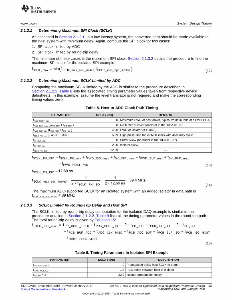
2.1.3.3 SCLK Limited by Round-Trip Delay and Host SPIThe SCLK limited by round-trip delay computation for the isolated DAQ example is similar to theprocedure detailed in Section 2.1.2.2. Table 9 lists all the timing parameter values in the round-trip path.The total round-trip delay is given by Equation 15:
(15)
Table 9. Timing Parameters in Isolated SPI Example
PARAMETER DELAY (ns) DESCRIPTIONtPD_HOST_SCLK 0 Propagation delay host SCLK to outputtPCB_HOST_ISO 1.5 PCB delay between host to isolatortPD_ISO × 2 32.0 Isolator propagation delay

( )SCLK _ max SCLK _ max _ adc _ limited SCLK _ max _ host _ limitedf min f , f=
ADC _ SAMPLECLK _ maxCONVST _ CYCLE _ min CONV SCLK _ min
1 1f
t t N t
æ ö æ ö= =ç ÷ ç ÷
ç ÷ ç ÷+ ´è ø è ø
SCLK _min_rtpd_ limited RTPD_ISO _max
SCLK _max _rtpd_ limited 9
t 2 t
1f 12.1MHz
2 41.2 10-
³ ´
= @
´ ´
System Design Theory www.ti.com
14 TIDUCM8A–December 2016–Revised January 2017Submit Documentation Feedback
Copyright © 2016–2017, Texas Instruments Incorporated
20-Bit, 1-MSPS Isolator Optimized Data Acquisition Reference DesignMaximizing SNR and Sample Rate
Table 9. Timing Parameters in Isolated SPI Example (continued)PARAMETER DELAY (ns) DESCRIPTION
tPCB_ISO_BUF 0 PCB delay between Isolator to buffer or level translatortPD_BUF × 2 0 Buffer or level translator propagation delaytPCB_BUF_ADC 0 PCB delay between buffer to ADCtADC_CLK_MISO 6.5 ADC clock to output delaytPCB_ADC_BUF 0 PCB delay between ADC to buffertPCB_BUF_ISO 0 PCB delay between buffer to isolatortPCB_ISO_HOST 0 PCB delay between isolator to hosttHOST_SCLK_MISO 1.2 Setup time of host MISO linetRTPD_ISO_max 41.2 —
The minimum SCLK period limited by the round-trip delay is:
(16)
Hence, fSCLK_max = 12 MHz.
The round-trip delay limits the SPI SCLK to 12 MHz; any delay added in the round-trip path furtherreduces the maximum SCLK.
2.1.3.4 Determining Maximum ADC Sample ClockThe maximum ADC sampling clock rate computation procedure is same as described in Section 2.1.2.4,and Equation 11 is repeated for reference:
(17)
The ADC sampling clock rate for a different SDO line configuration is calculated using Equation 17 andlisted in Table 10.
Table 10. Maximum ADC Clock and SDO LineConfiguration
SDOx N fADC_SAMPLECLK_max
SDO[0] 20 508 kHzSDO[0..1] 10 1.1 MHzSDO[0..3] 5 1.4 MHz
These results shows the design needs at least two SDO lines to achieve a 1-MSPS sampling rate in thisisolated SPI example.
2.1.4 Maximizing Sample Rate With Source-Synchronous ModePart of TI’s family of high-performance SAR ADCs, both the ADS9110 and ADS8900B possess a source-synchronous feature that significantly overcomes the limitation of SCLK reduction due to round-trippropagation delay. The source-synchronous mode provides a clock output (on the RVS pin) synchronizedto the output data (SDOx data lines). The host can receive the data with a slave SPI. The maximum ADCsampling clock frequency is determined by selecting the minimum of SCLK limited by ADC and RVSlimited by the host.
(18)

SCLK _ max_ adc _ limitedSCLK _ min_ host _ limited
1 1f 27.6 MHz
2 t 2 18.1ns= = =
´ ´
SCLK _ min_ host _ limitedt 18.1ns=
SCLK _ min _ host _ limited RVS _ SCLKPH_ISO
SCLK _PH_ min PWD _BUF _ max SK _BUF _ max
PWD _ISO _ max SK _ISO _ max PWD _ ADC _ max
t t
t t t
t t t
=
= + +
+ + +
SCLK _max _adc _ limitedf 39 MHz@
SCLK _ max _ adc _ limitedSCLK _PH_ISO
1 1f 39.4 MHz
2 t 2 x 12.69 ns= = =
´
DQ
D Q
Level Translator
Isolator HostADC
SCLK_ADC
SDO-0_ADC
1.8 V 3.3 V 3.3 V
tADC_SCLK_MOSI
tPCB_BUF_ADC
tPWD_BUF_ADC
tPD_BUF
tPWD_BUF
tPCB_ISO_BUF
tPWD_ISO_BUF
tPD_ISO
tPWD_ISO
tPCB_ISO_HOST
tPWD_ISO_HOST
DQ
tHOST_SCLK_MISO
tHOST_CLK_Q
SCLK Gen
SDI_0_HOST
RVS_HOST
SCLK_HOST
Copyright © 2017, Texas Instruments Incorporated
RVS_ADC
www.ti.com System Design Theory
15TIDUCM8A–December 2016–Revised January 2017Submit Documentation Feedback
Copyright © 2016–2017, Texas Instruments Incorporated
20-Bit, 1-MSPS Isolator Optimized Data Acquisition Reference DesignMaximizing SNR and Sample Rate
Figure 11. Isolated SPI in Source-Synchronous Mode
2.1.5 Determining Maximum SCLK Limited by ADC and HostComputing the maximum SCLK limited by the ADC is described in Section 2.1.3.2. A level translator is notrequired, and corresponding timing values are made zero.
(19)
Hence the maximum SCLK limited by ADC is:
Similarly, the SCLK limited by the host can be computed as:
(20)
Table 11. ADC-to-Host Clock Path Timing
PARAMETER DELAY (ns) REMARK
tSCLK_PH_min (0.45 × 2 × 12.69) 11.4 High pulse time for fSCLK_max_adc_limited clock with 45% dutycycle
tPWD_BUF_max (tPWD_BUF + tOD_BUF ) 0 No buffer or level translator in the TIDA-01037tSK_BUF_max 0 Buffer skew (no buffer in the TIDA-01037)tPWD_ISO_max (tPWD_ISO + tOD_ISO ) 4.2 PWD of the isolator (ISO7840)tPWD_ADC_max 0 Maximum PWD of ADC SDO output linestSK_ISO_max 2.5 Isolator skewtRVS_SCLKPH_ISO 18.1 —
(21)
(22)
The value of the PCB trace delay does not matter if the user can route RVS and SDOx at equal lengthand keep the differential length to a minimum. The differential length between RVS and SDOx results inskew, and that has to be considered for tRVS_SCLKPH_ISO calculation.

( )in jitterSNR 20 log 2 f t 10 log OSR( )= - p ´ +
System Design Theory www.ti.com
16 TIDUCM8A–December 2016–Revised January 2017Submit Documentation Feedback
Copyright © 2016–2017, Texas Instruments Incorporated
20-Bit, 1-MSPS Isolator Optimized Data Acquisition Reference DesignMaximizing SNR and Sample Rate
Hence with fSCLK_max = 27.6 MHz, the maximum ADC sampling rate is computed for different SDOx lineconfiguration and listed in Table 12.
Table 12. Maximum ADC Sample Rate in Source-Synchronous Mode
SDOx N fADC_SAMPLECLK_max
SDO[0] 20 975 kHzSDO[0..1] 10 1.5 MHzSDO[0..3] 5 2.0 MHz
Table 12 shows that it possible to achieve a sampling rate of 2 MSPS using source-synchronous modeand a multiSPI™ configuration.
2.1.6 Concluding RemarksThe document provides a comprehensive timing analysis for non-isolated and isolated ADC interfaces.The objective of the timing analysis is to determine the maximum ADC sampling rate and the maximumSPI clock to maximize ADC sample rate. The maximum SPI clock ensures minimum latency. Digitalisolators have large propagation delays, which limit the maximum SPI clock. Source-synchronous modeand a multiSPI configuration makes it possible to achieve a high sampling rate with digital isolators.
2.2 Additive Jitter Due to Digital IsolatorThe ADC SNR performance is a function of sampling clock jitter at a high input signal frequency. Thedigital isolator’s additive jitter to the sample clock limits the signal chain SNR. To the first order, the jitterimpact on SNR can be calculated as:
(23)
where:• fin is the input signal frequency• tjitter is the total jitter of the ADC (internal clock + external clock)• OSR is the over sampling ratio (only for sigma-delta ADC)
As can be seen in Figure 12, the SNR impact from jitter increases with the signal frequencies because itresults in a larger measurement error. Find more details in the TIDA-00732 design guide, 18-Bit, 2-MSPSIsolated Data Acquisition Reference Design for Maximum SNR and Sampling Rate (TIDUB85).
Figure 12. Error Due to Jitter on Sampling Clock
D
HOST CONTROLLER
ADC
ISOLATOR
Round trip delay period
D0 D1 D2MOSI
SCLK
D0 D1 D2MISO_1
SCLK_3
D0 D1 D2MOSI_1
D0 D1 D2MISO_1
SCLK_1
SCLK_2
SCLK
MOSI
MISO_1
SCLK_3
SCLK_1
MOSI_1
MISO(SDO0)
SCLK_2Source synchronous
mode at ADC
Copyright © 2017, Texas Instruments Incorporated
www.ti.com System Design Theory
17TIDUCM8A–December 2016–Revised January 2017Submit Documentation Feedback
Copyright © 2016–2017, Texas Instruments Incorporated
20-Bit, 1-MSPS Isolator Optimized Data Acquisition Reference DesignMaximizing SNR and Sample Rate
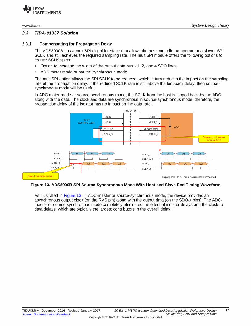
2.3 TIDA-01037 Solution
2.3.1 Compensating for Propagation DelayThe ADS8900B has a multiSPI digital interface that allows the host controller to operate at a slower SPISCLK and still achieves the required sampling rate. The multiSPI module offers the following options toreduce SCLK speed:• Option to increase the width of the output data bus - 1, 2, and 4 SDO lines• ADC mater mode or source-synchronous mode
The multiSPI option allows the SPI SCLK to be reduced, which in turn reduces the impact on the samplingrate of the propagation delay. If the reduced SCLK rate is still above the loopback delay, then source-synchronous mode will be useful.
In ADC mater mode or source-synchronous mode, the SCLK from the host is looped back by the ADCalong with the data. The clock and data are synchronous in source-synchronous mode; therefore, thepropagation delay of the isolator has no impact on the data rate.
Figure 13. ADS8900B SPI Source-Synchronous Mode With Host and Slave End Timing Waveform
As illustrated in Figure 13, in ADC-master or source-synchronous mode, the device provides anasynchronous output clock (on the RVS pin) along with the output data (on the SDO-x pins). The ADC-master or source-synchronous mode completely eliminates the effect of isolator delays and the clock-to-data delays, which are typically the largest contributors in the overall delay.

CONVST
#CS
SCLK
SDI
SDO (0 ± 3)
(READY/CLK)RVS
ADC
60-Pin (30x2) 6DPWHF
connector
I2C
PHI
#CS_ISO
SCLK_ISO
SDI_ISO
SDO(0 ± 3)_ISO
RVS_ISO
#CS
SCLK
SDO
RCLK
SDI(0 ± 3)
CONVST_ISO
High Speed (ISO784x)
Low Jitter (ISO734x)
SYS_CLK
CONVST
Q
Prog- OSCOptional block to reduce jitter addedby host on CONVST
Low-jitter signal path
High-speed signal path
DD
Copyright © 2017, Texas Instruments Incorporated
System Design Theory www.ti.com
18 TIDUCM8A–December 2016–Revised January 2017Submit Documentation Feedback
Copyright © 2016–2017, Texas Instruments Incorporated
20-Bit, 1-MSPS Isolator Optimized Data Acquisition Reference DesignMaximizing SNR and Sample Rate
2.3.2 Mitigating SNR Degradation Due to JitterAny sample clock (CONVST) jitter will degrade ADC SNR performance at high input signal frequencies,which reduces system performance, as defined by Equation 23 and outlined in detail by the TIDA-00723TI Design. Generating a CONVST signal with a low-jitter oscillator will minimize mitigate jitter, improvingSNR performance by nearly 12 dB as demonstrated by the TIDA-00732 and TIDA-01035 designs.However, such solutions may not be feasible for host-controlled sample clocks, but minimizing additivejitter while maximizing the sample clock is still desired.
In order to optimize performance, two isolators are used. The ISO734x family is used to isolate the jittersensitive sampling clock because it possesses an adequate signaling speed and low jitter. Note that thesampling clock will always be a frequency (can be determined using Equation 11) below SPI, and itsisolator signaling speed is not normally a design constraint. However, isolator propagation delay andsignaling directly impacts SPI data throughput (CS, SCLK, SDO, SDIx lines). SPI lines are jitter tolerantand the ISO784x is used to maximize data without additive jitter concerns. Table 13 highlights theISO734x and ISO784x performance, and when used together, they can optimize the DAQ SNR and thesample rate.
Table 13. Isolator Jitter From Datasheet
ISOLATOR JITTER (pk-pk) SPEED PROPAGATION DELAYISO784x 900 ps at 3.3 V 100 Mbps 11 nsISO734x 130 ps at 3.3 V 25 Mbps 31 ns
Figure 14 illustrates the optimized DAQ design. A host-generated ADC sample clock (CONVST) is derivedfrom the system clock, SYS_CLK, and uses the low-jitter signal path enabled by the ISO734x. High-speedsignaling is achieved with the ISO784x for the SPI data lines (CS, SCLK, SDI, SDO[3:0], and RVS).Furthermore, the TIDA-01037 possesses an optional jitter cleaner circuitry that can be used to reducehost-generated CONVST jitter. This circuitry contains a low-jitter clock generator used to re-clock theCONVST (generated by the host) with SYS_CLK to remove the jitter added by the host.
Figure 14 shows the datasheet jitter specification of the isolator used in the TIDA-01037 design.
Figure 14. TIDA-1037 Optimized Block Diagram for Isolated DAQ

OD
IN F FLT FLT
V RF
V RS 1 j2 f RF C 1 j2 f 2 R C
1 1æ ö
+ p ´ + p
æ ö= ´ ´ç ÷ ç ÷
è ø è ´ ø´
20-Bit1 MSPS
SAR ADC
SMA Connector
VIN+
VIN-
IN+
IN-
+
5V_ISO
AVDD DVDD
3.3 V_ISO
_
_+ Vocm
THS4551
ADS8900B
RFLT = 22.1
CFLT = 1nF
RF = 1 N
CF = 1 nF
RF = 1 N
CF = 1 nF
R = 0
R = 0
RS = 1 N
RS = 1 N
Anti- aliasing Filter, Band limit noise from
Front end circuit
Input buffer with unity gain
Differential Input filter to remove external
noise
RFLT = 22.1
2.5 V
1
2
3
CFLT = 500 pF
CFLT = 500 pF
Copyright © 2016, Texas Instruments Incorporated
www.ti.com System Design Theory
19TIDUCM8A–December 2016–Revised January 2017Submit Documentation Feedback
Copyright © 2016–2017, Texas Instruments Incorporated
20-Bit, 1-MSPS Isolator Optimized Data Acquisition Reference DesignMaximizing SNR and Sample Rate
2.4 Circuit DesignTo optimize the performance of the 20-bit, 1-MSPS DAQ system, the input buffer, anti-aliasing filter, andreference driver must be designed in such a way that the performance is equal to or greater than the ADCperformance.
2.4.1 Analog Input Front End (Input Buffer and Anti-Aliasing Filter)Figure 15 describes the TIDA-01037’s AFE, which highlights the differential input filter, high output drivedifferential input buffer, and anti-aliasing filter. A high-speed, fully differential amplifier (FDA) with aprogrammable output common mode is well suited to drive the data converter due to its inherent nature toincrease immunity to external common-mode noise and reduce even order harmonics.
Figure 15. TIDA-01037 AFE
The TIDA-01037 is designed with the THS4551 FDA configured as an unity gain second-order active low-pass filter, which drives the 20-bit, 1-MSPS ADS8900B SAR ADC at full dynamic range. The transferfunction of this filter is determined by Equation 24:
(24)
The amplifier gain is determined by the RF and RS ratio and both were chosen to be 1 kΩ, so the FDA isconfigured as an unity gain buffer. In order to satisfy the design’s targeted specifications of supporting100-kHz input signals, the anti-aliasing filter cutoff frequency was designed to be ≅ 4 MHz. The differentialmode capacitor added across the filter output helps remove high-frequency differential noise and increaseTHD performance. Take care to select passive components with minimum voltage and temperaturecoefficients to preserve THD performance for varying input and temperature conditions.

REFIN_ADS8900B VIN2
TEMP3
GND4
TRIM/NR5
VOUT6
U31A
REF5050AIDGKT 1µFC94
5V_ISO
AGND_ISO
0.22R93
10µF
C96
AGND_ISO
AGND_ISO
( +5.2 V )( +5.0 V )
10µF
C88
Copyright © 2016, Texas Instruments Incorporated
NREF CONV _MAX
BUF _FLTREF
I T 2C
V
´ ´
=
System Design Theory www.ti.com
20 TIDUCM8A–December 2016–Revised January 2017Submit Documentation Feedback
Copyright © 2016–2017, Texas Instruments Incorporated
20-Bit, 1-MSPS Isolator Optimized Data Acquisition Reference DesignMaximizing SNR and Sample Rate
2.4.2 Reference Buffer CircuitThe reference driver circuit, illustrated in Figure 16, generates a voltage of 5-V DC using a single 5.2-Vsupply. This circuit is suitable to drive the reference of the ADS8900B at higher sampling rates up to 1MSPS. The reference voltage of 5 V in this TI Design is generated by the high-precision, low-noiseREF5050 circuit. The output broadband noise of the reference is heavily filtered by a low-pass filterformed by resistor R90 and capacitor C88.
The RBUF_FLT is R93, and the CBUF_FLT is C96 at the output of the reference driving ADC reference input.The value of RBUF_FLT and CBUF_FLT can be found using Equation 25:
(25)
Figure 16. Reference Buffer Circuit

AGND_ISO
1µFC101
AGND_ISO
1
2
3
4
5
U33OPA376AIDBVR
1µF
C9520.0k
R94
499
R96
5V_ISO
0.1µF
C97
AGND_ISO
AGND_ISO
VOCM
Buffer
1.00k
R95
1µFC100
AGND_ISO
49.9kR101
49.9k
R97
Vocm = VREF/2
VREF = 5 V
Divider
Copyright © 2016, Texas Instruments Incorporated
www.ti.com System Design Theory
21TIDUCM8A–December 2016–Revised January 2017Submit Documentation Feedback
Copyright © 2016–2017, Texas Instruments Incorporated
20-Bit, 1-MSPS Isolator Optimized Data Acquisition Reference DesignMaximizing SNR and Sample Rate
2.4.3 Common-Mode Voltage (VOCM)The external REF5050 high-precision, ultra-low noise, low-drift voltage reference generates both ADCvoltage reference and signal input common-mode to ensure the complete dynamic range of the isADS8900B used. The voltage is at a value of 2.5 V (5 V / 2) by using the REF5050 and the OPA376precision, low-noise amplifier as a buffer, as illustrated in Figure 17.
The FDA common-mode voltage (VOCM) should be at mid-supply to achieve maximum output dynamicrange. VOCM is derived from the supply voltage with resistive divider network. The VOCM voltage isbuffered using the OPA376 op amp within the loop compensation method. This configuration has goodstability when driving larger capacitive loads.
Resistor R96 is an isolation resistor that is connected in series between the op amp output and thecapacitive load to provide isolation and avoid oscillations. Capacitor C95 between the op amp output andthe inverting input becomes the dominant AC feedback path at higher frequencies. This configurationallows heavy capacitive loading while keeping the loop stable. The feedback resistor R94 helps tomaintain the output DC voltage same as the non-inverting input of op amp.
The value of resistor R96 has chosen such that lowers than 10% of load. The combination of resistor R95and capacitor C100 forms a low-pass filter with a cutoff frequency of 159 Hz. This filter will clean the rippleand noise.
Figure 17. Common-Mode Voltage
System Design Theory www.ti.com
22 TIDUCM8A–December 2016–Revised January 2017Submit Documentation Feedback
Copyright © 2016–2017, Texas Instruments Incorporated
20-Bit, 1-MSPS Isolator Optimized Data Acquisition Reference DesignMaximizing SNR and Sample Rate
2.4.4 Clock DesignThe clock source is an essential component in signal chain design, specifically when driving the ADCsample clock. Clock jitter directly impacts ADC SNR performance and becomes proportionally greater athigher input signal frequencies. It is important that the jitter from the selected clocking source will besignificantly less than the jitter introduced by the digital isolator.
This design has two master clock sources that can be used for ADC sample clock generation, jittercleaner logic, and host interface synchronization. Table 14 shows how to select one of the sources byproperly setting indicated resistor jumpers:• Crystal oscillator (3.3 V, 125 MHz, 50 ppm, low jitter, 1.9-ps jitter)• LMK61E2 - Programmable crystal oscillator (3.3 V, 150 MHz, 90-fs jitter)
Table 14. Master Clock Selection
SERIALNO MASTER CLOCK RESISTOR MOUNTING REMARKS
1 Crystal oscillatorR14: Populate
3.3 V, 125 MHz, 50 ppm, low jitter, 1.9-ps jitterR17: Do not populate
2 Programmable crystal oscillator(LMK61E2)
R14: Do not populate 3.3 V, 150 MHz, 90-fs jitter (Frequency ofoscillator must be programmed to 125 MHzthrough I2C interface)R17: Populate
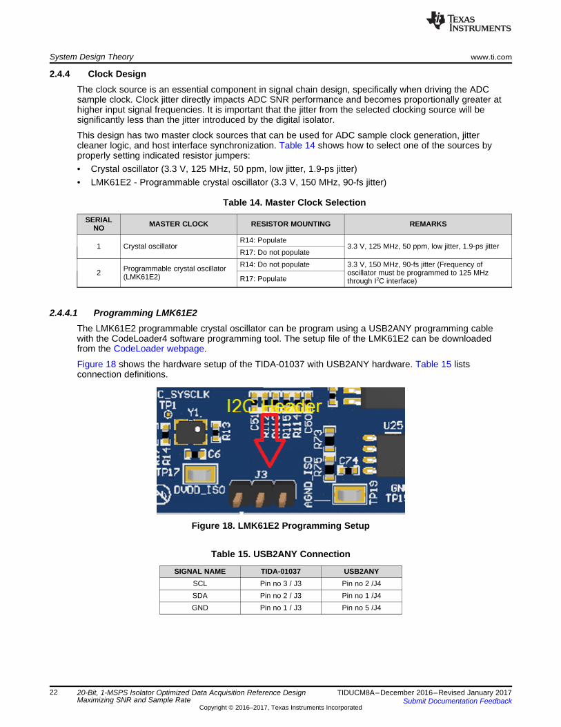
2.4.4.1 Programming LMK61E2The LMK61E2 programmable crystal oscillator can be program using a USB2ANY programming cablewith the CodeLoader4 software programming tool. The setup file of the LMK61E2 can be downloadedfrom the CodeLoader webpage.
Figure 18 shows the hardware setup of the TIDA-01037 with USB2ANY hardware. Table 15 listsconnection definitions.
Figure 18. LMK61E2 Programming Setup
Table 15. USB2ANY Connection
SIGNAL NAME TIDA-01037 USB2ANYSCL Pin no 3 / J3 Pin no 2 /J4SDA Pin no 2 / J3 Pin no 1 /J4GND Pin no 1 / J3 Pin no 5 /J4

www.ti.com System Design Theory
23TIDUCM8A–December 2016–Revised January 2017Submit Documentation Feedback
Copyright © 2016–2017, Texas Instruments Incorporated
20-Bit, 1-MSPS Isolator Optimized Data Acquisition Reference DesignMaximizing SNR and Sample Rate
2.4.4.1.1 Programming Procedure
1. Open the CodeLoder4 programming tool and select the LMK61E2 device.
Figure 19. Select Device
2. Go to the EZ Config tab. Under Output Configuration, enter "45" for MHz and the output type as"LVDS". Then generate the configuration and click the Program EEPROM button. Follow these steps(1 to 5) as shown in Figure 20.
Figure 20. Steps to Configure LMK61E2 GUI

ADC
SDO_1(0)
SDO_1(1)
SDO_1(2)
SDO_1(3)
SCLK
SDI
CS
RVS
CONVST
IsolatorDigital
ISO 7320
ISO 7841
ISO 7840
Copyright © 2017, Texas Instruments Incorporated
ADC
SCLK
SDI
RVS
SDO_1(0)
CONVST
IsolatorDigital
ISO 7320
ISO 7842
CS
Copyright © 2017, Texas Instruments Incorporated
ADC
RVS
SDO_1(0)
SCLK
SDI
CS
CONVST
IsolatorDigital
ISO 7320
ISO 7840
ISO 7840
Copyright © 2017, Texas Instruments Incorporated
ADC
SCLK
SDI
CS
SDO_1(0)
CONVST
IsolatorDigital
ISO 7320
ISO 7841
Copyright © 2017, Texas Instruments Incorporated
System Design Theory www.ti.com
24 TIDUCM8A–December 2016–Revised January 2017Submit Documentation Feedback
Copyright © 2016–2017, Texas Instruments Incorporated
20-Bit, 1-MSPS Isolator Optimized Data Acquisition Reference DesignMaximizing SNR and Sample Rate
2.4.5 Isolator Design and OptimizationIn order to provide the required system protection, the TIDA-01037 uses TI’s ISO1541, ISO734x, andISO784x family of high-performance isolated devices. The ISO784x series supports signaling rate up to100 Mbps, has a low 11-ns propagation delay, and operates from a wide supply voltage (2.25 to 5.5 V).The ISO734x series operates from a 3.3- to 5.5-V supply, possesses a very low jitter (≈ 130 ps) signalingrate up to 25 Mbps, and a typical propagation delay of 35 ns. These isolators are reinforced with very highimmunity possessing either a 3.0- or 5.7-kVRMS isolation voltage. The digital interface requires six isolationchannels for standard source-synchronous SPI communication and up to nine channels when fourmultiSPI outputs are used.
On the other hand, the ADC sampling clock requires just one ISO734x isolator channel. A single ISO1541bidirectional isolator is used for I2C communication to the optional jitter cleaner (see the TIDA-01035 TIDesign for more information).
The TIDA-01037 demonstrates how an isolated analog input can be optimized using six to nine isolatedchannels. In this example, illustrated in Figure 21, three digital isolators are required (one ISO734x andtwo ISO784x devices). More commonly, data converters lacking the source-synchronous mode andmultiSPI features will require just two isolator devices (one ISO734x and one IS784x), as illustrated inFigure 22.
Figure 21. TIDA-01037 Isolated DAQ Solution Using TI'sSource-Synchronous Mode
Figure 22. Typical Isolated DAQ Solution
Figure 23. Isolated DAQ Solution Using TI's Source-Synchronous Mode and Only Two Isolators
Figure 24. SNR and Sample Rate Optimized IsolatedDAQ Solution

FBT
5.62 KR 932
6= = W
FBT
FBB
R6
R=
FBT
FBB
R 5.61
R 0.8
æ ö= -ç ÷
è ø
www.ti.com System Design Theory
25TIDUCM8A–December 2016–Revised January 2017Submit Documentation Feedback
Copyright © 2016–2017, Texas Instruments Incorporated
20-Bit, 1-MSPS Isolator Optimized Data Acquisition Reference DesignMaximizing SNR and Sample Rate
Studying Figure 21, it is quickly realized that a more optimum solution would be able to move the CSsignal to the ISO7340 channel and replace the ISO7840 with an ISO7842 so the other ISO7840 can beeliminated as shown in Figure 23. Account for the propagation delay differences between the CS andother SPI signals (SCLK, SDI, and SDOx), and as a result, it may not practical. A more desirable andoptimized solution for high-speed signaling is illustrated in Figure 24. TI’s multiSPI feature is used tominimize SPI frequency and maximize ADC sample rate across the isolation boundary where threeadditional SPI outputs (SDO1-3), and thus three additional isolated data channels, are required. However,this solution still requires only three digital isolators while maximizing the features provided by the ADC,resulting in better device utilization. Similar to the previous solution, take care to match the propagationdelays between the ISO7841 and ISO7840 devices; however, they do both possess similar nominalpropagation delays.
Table 16. Required Number of Isolators for Common DAQ SystemsDATA LINES ONE DATA LINE SDO(0) TWO DATA LINES SDO(0:1) FOUR DATA LINES SDO(0:3)
ISO xxxx 7320/7340 7840 7841 Total 7320/7340 7840 7841 Total 7320/7340 7840 7841 Total
Single analoginput 1 0 1 2 1 2 0 3 1 2 0 3
Dual analog input 1 3 0 4 1 3 0 4 1 4 0 5
Quad analoginput 1 4 0 5 1 5 0 6 1 7 0 8
Eight analog input 2 8 0 10 2 10 0 12 2 14 0 16
Table 17. Required Number of Isolators for DAQ Systems Using Source-Synchronous ModeDATA LINES ONE DATA LINE SDO(0) TWO DATA LINES SDO(0:1) FOUR DATA LINES SDO(0:3)
ISO xxxx 7320/7340 7840 7841 Total 7320/7340 7840 7841 Total 7320/7340 7840 7841 Total
Single analoginput 1 0 1 2 1 1 1 3 1 1 1 3
Dual analoginput 1 1 2 4 1 1 2 4 1 2 2 5
Quad analoginput 1 5 0 6 1 6 0 7 1 8 0 9
Eight analoginput 2 10 0 12 2 12 0 14 2 16 0 18
2.4.6 Power Supply SolutionThis TI Design requires isolated and non-isolated power rails to various components. The following sectionprovides a detailed design procedure for the various power supply rails.
2.4.6.1 DC-DCThe LMZ14203TZ-ADJ simple switcher is capable of accepting a 6- to 46-V DC input and deliver a 0.8- to6-V output with 90% efficiency. The undervoltage lockout is selected at 7.97 V, which helps to enable theLMZ4203TZ-ADJ.
To set a 5-V output voltage, the resistor RFBT (R25) and RFBB (R31 + R36) decide the output voltage of theLMZ14203TZ-ADJ. For a 5.6-V output:
(26)
(27)
Therefore, R25 = 5.62K , R31 = 931 Ω, and R36 = 1 Ω.

10µFC24
GND
+12VDC_IN
MBRS4201T3G
200VD2
FB
118kR24
20.5kR34
249kR26
0.0
22µ
F
C20
0.01µF
C27
10µF
C22
10µFC23
VIN1
EN3
SS5
GND4
FB6
RON2
VOUT7
EP8
U5
LMZ14203TZ-ADJ/NOPB
+12VDC
5.62kR25
549R31
392R36
GND GND
GND
GNDGND
1
2
J5
8718
TP4 TP5
( +5.6 V )
Copyright © 2016, Texas Instruments Incorporated
System Design Theory www.ti.com
26 TIDUCM8A–December 2016–Revised January 2017Submit Documentation Feedback
Copyright © 2016–2017, Texas Instruments Incorporated
20-Bit, 1-MSPS Isolator Optimized Data Acquisition Reference DesignMaximizing SNR and Sample Rate
Figure 25. DC-DC Power Supply
2.4.6.2 LDOsThe TPS7A4700 is a positive voltage (36 V), ultra-low-noise (4 μVRMS) LDO capable of sourcing a 1-Aload. The TPS7A470x is designed with bipolar technology primarily for high-accuracy, high-precisioninstrumentation applications where clean voltage rails are critical to maximize system performance. Thisfeature makes the device ideal for powering op amps, ADCs, DACs, and other high-performance analogcircuitry.
The TPS7A4700RGWR has ANY-OUT™ programmable pins to program the desired output voltage. Thesum of the internal reference voltage (VREF = 1.4 V) plus the accumulated sum of the respective voltage isassigned to each active pins. The ANY-OUT pins (Pin 8, Pin 1, and Pin 12) are programmed to active lowto get 3.3 V at the output.
The TPS709 series of linear regulators are ultra-low quiescent current devices designed for powersensitive applications. A precision band gap and error amplifier provides 2% accuracy over temperature.The LDO can accept 2.7- to 30-V input voltages and deliver fixed output voltages 1.2 to 6.5 V with amaximum 200-mA output current. The TPS70918DBVT generates 1.8- from 5-V DC of the LMZ14203TZ-ADJ DC-DC converter.
2.4.6.3 Push-Pull TransformerThe SN6501 is a transformer driver designed for low-cost, small form-factor, isolated DC-DC convertersusing push-pull topology. The device includes an oscillator that feeds a gate-drive circuit. The gate drive,comprising a frequency divider and a break-before-make (BBM) logic, provides two complementary outputsignals that alternately turn on and off the two output transistors.
The SN6501 transformer driver is designed for low-power push-pull converters with input and outputvoltages in the range of 3 to 5.5 V. While converter designs with higher output voltages are possible, takecare that higher turns ratios do not lead to primary currents that exceed the SN6501 specified currentlimits.
The TIDA-01037 uses the recommended transformer inform the SN6501 datasheet. For transformerselection and isolation power supply design, see the SN6501 datasheet. Table 18 shows key parametersof the transformer.
Table 18. Transformer Specification
PARAMETER VALUEVoltage—time 11 µs
Turns ratio 1.1:1 ± 2%Switching frequency 150 kHz min
Di electric 6250 rms, 1 second

Isolated Differential Analog Inputs
Isolated power supply(ADC side)
Non-isolated power supply (Host side)
+12 V DC
Digital isolatorOptional block to reduce isolator
added jitter on CONVST
Host Interface Connector (PHI)
Analog Front End(FDA,ADC,
REFERENCE)
1
2
Isolation Transformer
3
4
5
6
7
8
9
ADS8900B
REF5050OPA376
THS4551
TPSA4700
TPS70918
LMZ14203
PHI
ISO7340
ISO7840
ISO7842
ISO7840
ISO5141LMK61E2
LMK61E2
SN74AUP1G80
SN74AHC1G04
SN74AUP1G80
750313734
10
Optional block to reduce host added jitter on CONVST
Copyright © 2017, Texas Instruments Incorporated
www.ti.com Getting Started Hardware and Software
27TIDUCM8A–December 2016–Revised January 2017Submit Documentation Feedback
Copyright © 2016–2017, Texas Instruments Incorporated
20-Bit, 1-MSPS Isolator Optimized Data Acquisition Reference DesignMaximizing SNR and Sample Rate
3 Getting Started Hardware and Software
3.1 Host InterfaceThe system performance of the TIDA-01037 can be evaluated using TI’s precision host interface (PHI)controller. PHI is TI’s SAR ADC evaluation platform, which supports the entire TI SAR ADC family. Byusing PHI, the TIDA-01037 can easily communicate with the host PC using a USB interface. PHI supportsthe ADS8900B multiSPI and onboard configuration I2C EEPROM interface. PHI GUI software canevaluate both the AC and DC parameters of the ADS8900B.
For more information on PHI, see the ADS8900B EVM-PDK.
3.2 Hardware Functional Block
Figure 26. TIDA-01037 Hardware
Figure 26 shows various hardware functional blocks of the TIDA-01037 and function of each block:1. 12-V DC power supply input connector that accepts 9- to 12-V DC input to power the TIDA-010372. Host-side DC-DC buck convertor that generates 5 V from the 12-V input3. Isolation transformer for power supply isolation and isolated power that is generated with the SN6501
push-pull transformer driver4. Isolated power supply rails block that generates 5-V, 3.3-V, and 1.8-V power rails5. Differential analog inputs connector6. AFE circuits (ADC ADS8900B, THS4551, and REF5050)7. Optional jitter mitigation block to reduce jitter on ADC side8. Digital isolator for data isolation (SPI and I2C)9. PHI interface connector, which uses the TIDA-01037 to communicate with the host PC through USB
interface10. Optional jitter mitigation logic block to reduce host added jitter on CONVST

ISO7340
ISO7840
ADC
CONVST
HOST
SPI Bus
S_SCSS_SCLK
S_SDO[3:0]S_SDI
H_SCSH_SCLKH_SDI[3:0]H_SD0
ISO7840
U15
U11
J15H_CONVSTOptional Jitter
mitigation logic
ADC
Copyright © 2016, Texas Instruments Incorporated
Getting Started Hardware and Software www.ti.com
28 TIDUCM8A–December 2016–Revised January 2017Submit Documentation Feedback
Copyright © 2016–2017, Texas Instruments Incorporated
20-Bit, 1-MSPS Isolator Optimized Data Acquisition Reference DesignMaximizing SNR and Sample Rate
3.2.1 Operation ModeThe TIDA-01037 hardware had provision to compare the performances of the low-jitter isolator and high-speed isolator using mode selection as illustrated in Figure 27. Table 19 shows the jumper configurationfor CONVST path selection.
Figure 27. CONVST Isolator Path Jumper Selection
Table 19. Operation Mode Jumper Setting
JUMPER SETTING DESCRIPTIONJ15—1, 2 Short CONVST signal passed through ISO7840 isolator and connected to ADC sample clock inputJ15—2, 3 Short CONVST signal pass through ISO7340 isolator and connected to ADC sample clock input
3.3 Getting Started Application GUIThe PHI GUI software, which is based on the LabVIEW™ platform, validates the TIDA-01037. Figure 28shows the available test options in the PHI GUI.
Figure 28. PHI GUI Demonstrate AC Parameter Analysis (Spectral and Time Domain)
The PHI GUI can be used to validate the following system key specifications:1. Spectral analysis
• SNR• THD• SFDR• SINAD• ENOB
2. Linearity analysis• DNL• INL• Accuracy
3. Histogram analysis• Effective resolution
Find the PHI GUI software at the ADS8900B product page.

PHI
TIDA-01037
Ultra-lowdistortion function
generator
Diff ± Input signal5 Vpp, 100 kHz
USBinterface
DC Power supply
12 V-DC
100-kHzBandpass filter
Copyright © 2016, Texas Instruments Incorporated
www.ti.com Testing and Results
29TIDUCM8A–December 2016–Revised January 2017Submit Documentation Feedback
Copyright © 2016–2017, Texas Instruments Incorporated
20-Bit, 1-MSPS Isolator Optimized Data Acquisition Reference DesignMaximizing SNR and Sample Rate
4 Testing and Results
4.1 Test SetupFigure 29 shows the TIDA-01037 test setup to validate complete signal chain performance of isolatedhigh-speed, high SNR (20-bit, 1-MSPS) analog input DAQ module.
The test needs to evaluate the performance of a high-speed (1-MSPS) and high-resolution (20-bit) systemthat is compliant with testing requirements. The setup has a DS360, a standard research systemsprecision ultra-low distortion waveform generator, which is capable of generating a sine pattern with asignal frequency range of 10 MHz to 200 kHz. The device needs high precision with a very low ripplepower supply to power the entire system. This TI Design requires 9- to 12-V DC at 250 mA with highprecision and low ripple power. The 12-V DC voltage is generated using a Keithley triple output powersupply (2230G). It is capable of generating up to 30 V with 0.03% voltage accuracy and 0.1% currentaccuracy with simultaneous voltage and current indication.
The data capturing is established using a USB 2.0 interface. The testing computer must have one USBport and must support USB 2.0 specification.
Sometimes, the signal source may also have noise on top of the signal while generating a sine wave with100 kHz. To remove this unwanted noise, a 100-kHz differential band-pass filler is connected in betweenthe signal source and the TIDA-01037 input connector. This filter will attenuate input noise at a 100-kHzband.
Figure 29. TIDA-01037 Test Setup
Install the PHI GUI software in the host computer before testing:1. Plug the PHI interface board into the Samtec connector (J1).2. Configure the operation mode using programmable resistor jumper (see Section 3.2.1).3. Connect 12-V DC of power to the J5 connector. Ensure the positive terminal is connected to the
positive input (Pin 2 of J5) and the negative terminal is connected to the negative input (Pin 1 of J5).4. Connect the differential output of function generator to the differential input terminal (J8 and J9 SMA
connector) of the TIDA-01037 board (for a 100-kHz input signal frequency, connect the 100-kHz bandpass filter in between the signal source and the TIDA-01037 board). Also, make sure both differentialsignals are balanced and configured as shown in Figure 29.
5. Connect the PHI module to the PC or laptop using a micro USB cable.6. Switch on the power supply.7. Switch on the signal source and set the signal source parameter. Then, enable the output.8. Run the PHI GUI software, go to the spectrum analysis tab, and capture result (SNR, THD, and ENOB)
with various input signal frequencies.9. The test results taken for both 2-kHz and 100-kHz input frequency for both mode of operation as
described in Section 3.2.1.

Testing and Results www.ti.com
30 TIDUCM8A–December 2016–Revised January 2017Submit Documentation Feedback
Copyright © 2016–2017, Texas Instruments Incorporated
20-Bit, 1-MSPS Isolator Optimized Data Acquisition Reference DesignMaximizing SNR and Sample Rate
Table 20. Signal Source Test Conditions
PARAMETER VALUEPattern SineVoltage 7.23 Vpp (adjust to cover full input dynamic range)
Frequency 2 kHz and 100 kHzSource impedance 600 Ω
Power supply 12-V DC at 250 mA
The test results are taken for both 2-kHz and 100-kHz input frequency with and without jitter cleanermode.
NOTE:1. While testing with a 100-kHz input signal frequency, a bandpass filter is used in between
the signal source and the TIDA-01037 module.2. Populated corresponding resistor jumper for with or without jitter mitigation mode.
4.2 Performance Test ResultsMeasured results for both 2-kHz and 100-kHz inputs are summarized in Table 21 and Figure 30. Theseresults are compared to ADS8900B data sheet which is used as an ideal performance goal. Measuredresults clearly indicate the benefits used both isolator families as part of a comprehensive solution. Forexample, the signal chain will realize nearly a 14-dB gain, 2.25-bit ENOB improvement when using boththe ISO7340 and ISO7840 devices for a 100-kHz input signal. Furthermore, using the ADC multiSPIfeature allows requires only a maximum clock of 45 MHz while still operating the ADS8900B at itsmaximum 1 MSPS sample rate.
Table 21. Performance Test Result
PARAMETER ADS8900B DATASHEETSPECIFICATION
TIDA-01037
ISO7840 ONLY SOLUTION ISO7340 and ISO7840SOLUTION
Fin (kHz) = 2SCLK (MHz) 45Sample rate (MSPS) 1SNR (dB) 104.00 100.72 101.12THD (dB) –125.00 –121.62 –122.60ENOB 17.00 16.43 16.50Fin (kHz) = 100SCLK (MHz) 45Sample rate (MSPS) 1SNR (dB) 99.50 83.70 97.37THD (dB) –110.00 –112.60 –113.00ENOB 16.20 13.61 15.86

Input Frequency(kHz)
SN
R(d
Bc)
1 10 10070
75
80
85
90
95
100
105
110
D001
CONVST via ISO784xCONVST via ISO734xADS8900B Spec
www.ti.com Testing and Results
31TIDUCM8A–December 2016–Revised January 2017Submit Documentation Feedback
Copyright © 2016–2017, Texas Instruments Incorporated
20-Bit, 1-MSPS Isolator Optimized Data Acquisition Reference DesignMaximizing SNR and Sample Rate
Figure 30. TIDA-01037 SNR Performance Graph
Figure 31. 2-kHz Spectrum—ISO7840 Only Solution Figure 32. 2-kHz Spectrum—ISO7340 and ISO7840Solution
Figure 33. 100-kHz Spectrum—ISO7840 Only Solution Figure 34. 100-kHz Spectrum—ISO7340 and ISO7840Solution

Design Files www.ti.com
32 TIDUCM8A–December 2016–Revised January 2017Submit Documentation Feedback
Copyright © 2016–2017, Texas Instruments Incorporated
20-Bit, 1-MSPS Isolator Optimized Data Acquisition Reference DesignMaximizing SNR and Sample Rate
5 Design Files
5.1 SchematicsTo download the schematics, see the design files at TIDA-01037.
5.2 Bill of MaterialsTo download the bill of materials (BOM), see the design files at TIDA-01037.
5.3 PCB Layout Recommendations
5.3.1 Layout PrintsTo download the layer plots, see the design files at TIDA-01037.
5.4 Altium ProjectTo download the Altium project files, see the design files at TIDA-01037.
5.5 Gerber FilesTo download the Gerber files, see the design files at TIDA-01037.
5.6 Assembly DrawingsTo download the assembly drawings, see the design files at TIDA-01037.
6 Software FilesTo download the software files, see the design files at TIDA-01037.
7 Related Documentation1. Texas Instruments, Noise Analysis in Operational Amplifier Circuits, Application Report (SLVA043)2. Texas Instruments, Fully-Differential Amplifiers, Application Report (SLOA054)3. Texas Instruments, Op Amp Noise Theory and Applications, Excerpted from Op Amps for Everyone
(SLOA082)4. Texas Instruments, 18-Bit, 2-MSPS Isolated Data Acquisition Reference Design for Maximum SNR and
Sampling Rate, TIDA-00732 Design Guide (TIDUB85)
7.1 TrademarksAll trademarks are the property of their respective owners.

www.ti.com About the Authors
33TIDUCM8A–December 2016–Revised January 2017Submit Documentation Feedback
Copyright © 2016–2017, Texas Instruments Incorporated
20-Bit, 1-MSPS Isolator Optimized Data Acquisition Reference DesignMaximizing SNR and Sample Rate
8 About the AuthorsANBU MANI is a systems engineer in the Industrial Systems Engineering team at Texas Instruments,where he is responsible for developing reference design solutions for the industrial segment. Anbu hasfifteen years of experience in analog circuit design and digital circuit design for the Automatic TestEquipment in Modular platform. He is also engaged with the design and development of embeddedproducts. Anbu earned his bachelor of engineering (BE) in electronic and communication from the AnnaUniversity, Chennai.
SANKAR SADASIVAM is a system architect in the Industrial Systems Engineering team at TexasInstruments, where he is responsible for architecting and developing reference design solutions for theindustrial systems with a focus on Test and Measurement. Sankar brings to this role his extensiveexperience in analog, RF, wireless, signal processing, high-speed digital, and power electronics. Sankarearned his master of science (MS) in electrical engineering from the Indian Institute of Technology,Madras.
HARSH MISRA is a project trainee in the Industrial Systems Engineering team at Texas Instruments,where he is learning developing reference design solutions for the industrial systems with a focus on Test& Measurement. Harsh is a final-year student pursuing a bachelor of engineering (B.E. hons) in electricaland electronics engineering from Birla Institute of Technology & Sciences (BITS), Pilani.

Revision A History www.ti.com
34 TIDUCM8A–December 2016–Revised January 2017Submit Documentation Feedback
Copyright © 2016–2017, Texas Instruments Incorporated
Revision History
Revision A HistoryNOTE: Page numbers for previous revisions may differ from page numbers in the current version.
Changes from Original (December 2016) to A Revision ................................................................................................ Page
• Changed language and images to fit current style guide ............................................................................ 1
IMPORTANT NOTICE FOR TI DESIGN INFORMATION AND RESOURCES
Texas Instruments Incorporated (‘TI”) technical, application or other design advice, services or information, including, but not limited to,reference designs and materials relating to evaluation modules, (collectively, “TI Resources”) are intended to assist designers who aredeveloping applications that incorporate TI products; by downloading, accessing or using any particular TI Resource in any way, you(individually or, if you are acting on behalf of a company, your company) agree to use it solely for this purpose and subject to the terms ofthis Notice.TI’s provision of TI Resources does not expand or otherwise alter TI’s applicable published warranties or warranty disclaimers for TIproducts, and no additional obligations or liabilities arise from TI providing such TI Resources. TI reserves the right to make corrections,enhancements, improvements and other changes to its TI Resources.You understand and agree that you remain responsible for using your independent analysis, evaluation and judgment in designing yourapplications and that you have full and exclusive responsibility to assure the safety of your applications and compliance of your applications(and of all TI products used in or for your applications) with all applicable regulations, laws and other applicable requirements. Yourepresent that, with respect to your applications, you have all the necessary expertise to create and implement safeguards that (1)anticipate dangerous consequences of failures, (2) monitor failures and their consequences, and (3) lessen the likelihood of failures thatmight cause harm and take appropriate actions. You agree that prior to using or distributing any applications that include TI products, youwill thoroughly test such applications and the functionality of such TI products as used in such applications. TI has not conducted anytesting other than that specifically described in the published documentation for a particular TI Resource.You are authorized to use, copy and modify any individual TI Resource only in connection with the development of applications that includethe TI product(s) identified in such TI Resource. NO OTHER LICENSE, EXPRESS OR IMPLIED, BY ESTOPPEL OR OTHERWISE TOANY OTHER TI INTELLECTUAL PROPERTY RIGHT, AND NO LICENSE TO ANY TECHNOLOGY OR INTELLECTUAL PROPERTYRIGHT OF TI OR ANY THIRD PARTY IS GRANTED HEREIN, including but not limited to any patent right, copyright, mask work right, orother intellectual property right relating to any combination, machine, or process in which TI products or services are used. Informationregarding or referencing third-party products or services does not constitute a license to use such products or services, or a warranty orendorsement thereof. Use of TI Resources may require a license from a third party under the patents or other intellectual property of thethird party, or a license from TI under the patents or other intellectual property of TI.TI RESOURCES ARE PROVIDED “AS IS” AND WITH ALL FAULTS. TI DISCLAIMS ALL OTHER WARRANTIES ORREPRESENTATIONS, EXPRESS OR IMPLIED, REGARDING TI RESOURCES OR USE THEREOF, INCLUDING BUT NOT LIMITED TOACCURACY OR COMPLETENESS, TITLE, ANY EPIDEMIC FAILURE WARRANTY AND ANY IMPLIED WARRANTIES OFMERCHANTABILITY, FITNESS FOR A PARTICULAR PURPOSE, AND NON-INFRINGEMENT OF ANY THIRD PARTY INTELLECTUALPROPERTY RIGHTS.TI SHALL NOT BE LIABLE FOR AND SHALL NOT DEFEND OR INDEMNIFY YOU AGAINST ANY CLAIM, INCLUDING BUT NOTLIMITED TO ANY INFRINGEMENT CLAIM THAT RELATES TO OR IS BASED ON ANY COMBINATION OF PRODUCTS EVEN IFDESCRIBED IN TI RESOURCES OR OTHERWISE. IN NO EVENT SHALL TI BE LIABLE FOR ANY ACTUAL, DIRECT, SPECIAL,COLLATERAL, INDIRECT, PUNITIVE, INCIDENTAL, CONSEQUENTIAL OR EXEMPLARY DAMAGES IN CONNECTION WITH ORARISING OUT OF TI RESOURCES OR USE THEREOF, AND REGARDLESS OF WHETHER TI HAS BEEN ADVISED OF THEPOSSIBILITY OF SUCH DAMAGES.You agree to fully indemnify TI and its representatives against any damages, costs, losses, and/or liabilities arising out of your non-compliance with the terms and provisions of this Notice.This Notice applies to TI Resources. Additional terms apply to the use and purchase of certain types of materials, TI products and services.These include; without limitation, TI’s standard terms for semiconductor products http://www.ti.com/sc/docs/stdterms.htm), evaluationmodules, and samples (http://www.ti.com/sc/docs/sampterms.htm).
Mailing Address: Texas Instruments, Post Office Box 655303, Dallas, Texas 75265Copyright © 2017, Texas Instruments Incorporated