2012 2013 stage-thesisgids update23oktober
TRANSCRIPT

Master Thesis/Internship Topic Guide 2012-2013

Master Thesis/Internship Topics 2012-2013
Information..........................................................................................................................................................................................1
I. CMOS Scaling R&D ................................................................................................................. 2
Defect characterization of hetero-epitaxial III-V layers for future high-performance sub-16 nm CMOS transistors .................................................................................................................................................................................... 2
Random Telegraph Noise (RTN) and the ITRS Roadmap: is it the beginning of the end? ..................................... 3
Deposition and characterization of dielectric barrier films ............................................................................................ 4
Using variational calculus to solve Poisson's and Schroedinger's equations self-consistently within a single loop: how far can we go? ......................................................................................................................................................... 5
Modeling of leakage in very high permittivity dielectrics for DRAM applications ..................................................... 5
Parallelization of CMOS time-dependent variability measurements............................................................................. 6
Low damage etch: use of CF3I as reactant for patterning of 2.0 porous SiOCH materials .................................... 7
Post-etch ULK restoration strategies: effect of H2-CH4-based plasma treatments on dielectric recovery of 2.0 porous SiOCH materials ................................................................................................................................................... 8
Plasma treatments of model polymers used in EUV lithography: PS and PMMA ...................................................... 9
Evaluation of photoresist outgassing for extreme ultraviolet lithography ................................................................ 10
Carbon nanotube contacts: electrical characterization of CNT – Cu damascene contacts ................................ 11
Graphene synthesis and characterization .......................................................................................................................... 12
Atomic layer deposition for applications in nanotechnology ....................................................................................... 13
XRD study of nano-structured hetero-epitaxial III-V compound semiconductors for VLSI CMOS applications ................................................................................................................................................................................ 14
Developing in-situ doping of III-V compound semiconductors by hetero-epitaxial MOCVD growth .............. 14
Surface preparation and interface passivation of high mobility channel materials for beyond 14 nm technology nodes ..................................................................................................................................................................... 15
Electrical evaluation and reliability assessment of local interconnects....................................................................... 16
Investigation of advanced resistance-switching (RRAM) memory cells ..................................................................... 16
Investigation and optimization of the electrical switching properties of Conductive Bridging RAM memory cells (CBRAM) .......................................................................................................................................................................... 17
Passivation of Ge for high-performance applications ..................................................................................................... 18
Graphene: device fabrication and characterization ......................................................................................................... 19
Graphene: device fabrication for optoelectronics ........................................................................................................... 20
Characterization of ohmic contacts to high-mobility materials (Ge, III-V) ............................................................... 21
Spin transfer torque magnetic random access memory ................................................................................................ 22
Wet processing of high aspect ratio nanostructures...................................................................................................... 23
Surface chemistry of III-V semiconductors for cleaning applications ......................................................................... 24
The creation of nanoforces by microbubbles ................................................................................................................... 25
Galvanic corrosion in micro-bump with different bumping metallurgy ..................................................................... 26
Direct heteroepitaxy of III-V semiconductors on silicon mediated by strain-relaxed buffer layers .................. 27

Master Thesis/Internship Topics 2012-2013
3D FIB/SEM structural analysis of nano-electronic devices .......................................................................................... 28
Carrier depth profiling with micro-probes on advanced ultra-shallow high-mobility CMOS semiconductor structures ................................................................................................................................................................................... 29
Development of a professional data analysis package for the micro-four point probe (M4PP) .......................... 30
Development of an industrial analysis-package in Visual C++ for SSRM-measurements ...................................... 31
Development of probes for nanoscale electrical measurements and manipulation in a nanoprober system ......................................................................................................................................................................................... 32
Diamond probes – more efficient and optimized yield assessment .......................................................................... 33
Advanced materials characterization using ion beam scattering ................................................................................. 34
Ultra high vacuum SSRM nanocontact modeling - Electrical and mechanical impacts of low temperatures (70K) ........................................................................................................................................................................................... 35
Atomic Layer Deposition of ultrathin metal films for advanced nanoelectronic applications ............................. 36
In-situ molecular beam passivation of III-Sb compounds ............................................................................................... 37
Developing in-situ doping of III-V compound semiconductors by hetero-epitaxial MOCVD growth ................ 37
Effect of confinement and position of dopants on the ionized impurity scattering limited mobility in a few-dopant double gate junctionless FET or all-around gate cylindrical nanowire junctionless transistor ...... 38
Characterization and modeling of the junctionless III-V nanowire for novel device applications ..................... 39
Remote Coulomb, surface roughness and ionized impurity scattering in novel nanowire all-around gate FET devices ................................................................................................................................................................................ 40
Symbolic analysis of logic cells for advanced technologies ............................................................................................ 41
Tailored functional oxides for nanoelectronics ............................................................................................................... 42
Defectivity monitoring of directed self-assembly ............................................................................................................ 43
II. CMORE ................................................................................................................................... 45
Design and modeling of a single sensor 3-axis gyroscope for IMUs (inertial measurement units) .................... 45
Capacitive micromachined ultrasound transducers for imaging, telecom and power transmission applications ................................................................................................................................................................................ 46
(NANO)PHononicS: MEMS/NEMS acoustic devices and circuits ............................................................................... 47
Nano relays and logic gates: designing at the nanoscale, in presence of nano adhesion forces .......................... 48
MEMS-based loudspeaker ...................................................................................................................................................... 49
III. Smart Systems ....................................................................................................................... 50
Measurement and calibration of models for advanced photovoltaic modules ......................................................... 50
Machine learning on low power parallel architectures .................................................................................................. 51
Algorithm and architecture co-optimizations for cost and power constrained Signal processing system ....... 52
Complexity modeling and algorithm transformations for software defined radios ................................................ 53
Collaborative spectrum sensing for cognitive radios ...................................................................................................... 54
Radio-frequency communication with metal-oxide electronics on plastic ............................................................... 55

Master Thesis/Internship Topics 2012-2013
IV. HUMAN++ .............................................................................................................................. 56
Investigating the long term behavior of TiN as electrode material for cell interfacing technologies ................ 56
Localized electrical stimulation of in vitro neurons for guided growth ..................................................................... 57
Signal analysis of recorded electrical activity by advanced microelectrode arrays ................................................. 58
Surface enhanced raman spectroscopy for studying cell-nanoparticle interactions ............................................... 58
Analog signal processing for medical signals ..................................................................................................................... 59
Multifunctional magnetic gold nanoparticles: chemical functionalization and applications .................................... 60
Development of multiparameter biointerfaces that can be implemented in different biosensor platforms .... 61
Development of multiparameter biointerfaces based on photoactive linkers ......................................................... 61
Bio-assay development in microfluidic channels .............................................................................................................. 62
Different surface functionalization strategies for silicon based biochips ................................................................... 62
Identification and characterization of circulating tumor cells ....................................................................................... 63
High speed microfluidic cell sorting .................................................................................................................................... 63
Ultra-sensitive diagnostic method based on surface enhanced Raman spectroscopy on plasmonic- magnetic beads.......................................................................................................................................................................... 64
Bridge PCR on optical sensors ............................................................................................................................................. 64
SERS measurement of kinase activity on synthetic peptides ........................................................................................ 65
Two photon lithography with plasmonic nanoantennas ................................................................................................ 66
Plasmonic 2D crystals with gain ........................................................................................................................................... 67
Combining neuronal signal processing algorithms into Matlab-based graphical user interface platform for analysis of in vivo brain signals .............................................................................................................................................. 68
Organotypic slice culture ....................................................................................................................................................... 69
V. Energy...................................................................................................................................... 70
Degradation mechanisms in organic solar cells ................................................................................................................ 70
Solving the Caldeira-Leggett model with balance equations ......................................................................................... 71
Modeling ionic diffusion in solid-state materials for energy storage applications.................................................... 71
Bonding of cells to glass for next-generation c-Si PV modules .................................................................................... 72
Metal contacts for amorphous Si solar cell applications ................................................................................................ 72
Radio-frequency communication with metal-oxide electronics on plastic ............................................................... 73
Morphological control of organic bulk solar cells ........................................................................................................... 74
Spectral characterization of organic tandem solar cells ................................................................................................. 75
Tunneling barriers for the passivation of metal contacts in silicon solar cells ......................................................... 75
Development of amorphous silicon deposition for silicon heterojunction solar cells........................................... 76
CIGSSe and CZTSSe films formation from selenization/sulfurization of metals and chalcogenide compounds ................................................................................................................................................................................ 77

Master Thesis/Internship Topics 2012-2013
Characterization and power-loss analysis of interdigitated back contact (IBC) silicon solar cells ..................... 78
Reliability testing of c-Si solar cells with Cu plated metallization ................................................................................ 79
Copper contact plating for advanced solar cell contacts .............................................................................................. 79
EBIC analysis of thin-film polycrystalline-silicon solar cells ........................................................................................... 80
Raman and EDS analysis for thin-film solar-cell applications ........................................................................................ 81
Organic solar-cell material characterization by TOF-SIMS ........................................................................................... 82
Characterization of organic materials using UHV conductive AFM at low temperatures .................................... 83
Characterization and modeling of Back-surface field formation in Si-based solar cells ......................................... 84
Initiation of random pyramid formation: impact of contamination and surface roughness .................................. 85
Photonic nanostructures for light management in novel thin silicon solar cells and modules............................. 86
Investigation on laser enhanced metal-silicide formation for novel front contact schemes on silicon solar cells .............................................................................................................................................................................................. 87
Investigation on laser enabled boron doping activation for novel silicon solar cell concepts ............................. 88
Circuit modeling of interconnection schemes for thin film PV modules ................................................................... 89
Alternative assembly technologies for next-generation c-Si PV modules ................................................................. 90
Deposition and characterization of a-Si layers to passivate epitaxial emitters on thin silicon foils on glass .... 91
Investigation on laser enabled boron doping activation for novel silicon solar cell concepts ............................. 92
VI. INVOMEC ............................................................................................................................... 93
Visualisatie van DfX analyse feedback in een elektronisch ontwerp .......................................................................... 93
Pre-routing metal layer estimation ...................................................................................................................................... 94
VII. NERF........................................................................................................................................ 95
Design, prototyping and testing of miniaturized brain implants .................................................................................. 95

1
Master Thesis/Internship Topics 2012-2013
Information
Students from universities and engineering schools can apply for a master thesis and/or internship project at imec. Imec offers topics in engineering and (industrial) sciences in different fields of research.
The topics are arranged according to the imec business programs. You can find more detailed information on each research program under the heading ‘Research’ on www.imec.be.
How to apply?
Send an e-mail with your motivation letter and detailed resume to the responsible scientist(s) mentioned at the bottom of the topic description of your preference. The scientist(s) will screen your application and let you know whether or not you are selected for a project at imec.
It is not recommended to apply for more than three topics.
For more information, go to the Internship and Master Thesis pages under the Education heading on our website.

2
Master Thesis/Internship Topics 2012-2013
I. CMOS Scaling R&D
Defect characterization of hetero-epitaxial III-V layers for future high-performance sub-16 nm CMOS transistors
As the silicon device scaling for future generations becomes increasingly difficult, alternative device structures and high mobility channel materials like Ge (P-type), InGaAs (n-type), InSb have gained popular research interests. However owing to high cost of III-V or Ge wafers, the active layers are proposed to be deposited epitaxially on silicon substrates. This presents itself as a challenge: due to the large lattice mismatch between Si and Ge or III-V materials, a high density of extended defects like misfit and threading dislocations, stacking faults, twins is created. Furthermore, the deposition of polar III-Vs on non-polar Si creates additional defects like polar and anti phase domains. It has been studied that these defects acts as non-radiative recombination centers and limits the electrical transport of carriers in the device. Therefore, it is important to characterize these defects on the basis of extent of performance degradation caused by them in the CMOS devices. Subsequently, based on these studies it is desired to introduce variants in the growth strategies to mitigate the harmful effects or completely eliminate them.
The focus of this internship/thesis would be to study the electrical properties of p-n junction diodes containing extended defects, fabricated under different processing conditions. This would be done by measuring Current-Voltage (I-V) and Capacitance-Voltage(C-V) characteristics. Temperature dependent measurements can also be carried out. The information about the generation and recombination lifetime, ideality factor, activation energy can be extracted from these measurements which in turn indicate the dominant mechanism (Shockley-Read-Hall, Field Assisted Tunneling) in the devices.
Additionally, defect characterization which involves identifying and classifying the defects can also be performed using facilities available at IMEC in close collaboration with its industrial partners.
Type of project: Thesis/internship of 3-4 months. Degree: Master in Industrial Sciences or Master in Science or Master in Engineering majoring in material science, physics, electronics.
Responsible scientist(s): For further information or for application, please contact Eddy Simoen ([email protected]) and Somya Gupta ([email protected]).

3
Master Thesis/Internship Topics 2012-2013
Random Telegraph Noise (RTN) and the ITRS Roadmap: is it the beginning of the end?
Low-frequency noise is present in all physical, electronic, biological and even societal systems and is for most experimentalists a source of error. However, it can also provide fundamental information on the basic transport mechanisms through a semiconductor device, for example. Flicker noise or 1/f noise appears to be universal in most large systems but breaks down when the dimensions reach the nanoscopic level. In the case of a MOSFET, it is believed that trapping and de-trapping of charge through many defect states is at the origin of the 1/f noise. When scaling the device dimensions to the sub-micrometer area, the number of active traps reduces, so that eventually, only one or a few traps are active and determine the charge transport fluctuations. In practice, this means that for a small-area device, the current through the channel can switch between a high and a low state, which is called Random Telegraph Noise (RTN). As the occurrence of a trap and associated RTN is a random process, this may give rise to significant variation from device to device. As such, RTN is a source of temporal device variability and may form a performance limitation for 16-nm and below CMOS memories. It is the aim of the work to study the low-frequency noise and RTN behavior of advanced CMOS technology devices and to investigate the possible impact of various process options. At imec, there is a computer-controlled noise measurement system, combined with a 300 mm probe station, allowing a detailed analysis in function of the gate and drain voltage. As RTN traps may also affect the mobility by scattering, a correlation with other device parameters, like the threshold voltage and the mobility will be looked for. It is also possible to study the RTN and noise behavior as a function of temperature. This enables the determination of the thermal activation of the emission and capture processes underlying the RTN and noise and provides information on the trap level energy and capture cross section. In a way, RTN allows for trap spectroscopy in small systems. As there is more and more interest from the industry, this work will be performed in close collaboration with the imec industrial Partners.
Type of project: Thesis of 3 months. Degree: Master in Science or Master in Engineering majoring in e.g. device physics. Responsible scientist(s): For further information or for application, please contact Eddy Simoen ([email protected]).

4
Master Thesis/Internship Topics 2012-2013
Deposition and characterization of dielectric barrier films
In copper interconnect technology, typically SiCN films are deposited in-between the low-k dielectric layers, serving at the same time as a etch stop layer, dielectric Cu barrier, and moisture barrier. Driven by the continuing scaling, requiring a lower overall k-value of the dielectric stack, alternative materials are investigated. These should have a lower k-value than SiCN, while maintaining the barrier and etch stop properties, or have similar properties at a lower thickness. In this project, the deposition process window is screened for a certain precursor, varying process conditions, based on literature research. This involves extensive characterization of the deposited films, starting with the determination of thickness, refractive index, chemical composition through FTIR, stress, Young’s modulus, hardness, porosity, hydrophilicity, dielectric constant, and leakage of the films. For the most promising films, a second series of tests which simulate other (former and later) process steps, is performed; this also includes tests to determine the adhesion to other films, mainly by 4 point bending analysis. Also, a more detailed chemical analysis, e.g. through XPS and TOFSIMS, will be performed. If all tests are positive, finally, the material is used in an integration process, resulting in a real test chip and the final electrical characterizations (including reliability characterizations) are made. The student will be strongly involved in both the actual deposition of the films and the detailed characterization of the basic film properties. Hereby (s)he will use state of the art equipment, such as an industrial PE-CVD reactor, ellipsometers, a Fourier Transform Infrared spectrometer, a high precision mass measurement system, and others. Furthermore (s)he will also be involved in the next phase of the characterization cycle, as setting up the processes for the simulation of integration aspects and the electrical characterization on test chips. Also, the student can be involved in setting up a practical test procedure to measure Cu barrier properties. Academic and industrial results will be reported in meetings where both imec staff and industrial affiliates participate.
Type of project: Thesis or internship of minimum 5 months, to start in 2013. Degree: Master in Science or Master in Engineering majoring in material science, physics, electronics. Responsible scientist(s): For further information or for application, please contact Els Van Besien ([email protected]).
5
Master Thesis/Internship Topics 2012-2013
Using variational calculus to solve Poisson's and Schroedinger's equations self-consistently within a single loop: how far can we go?
Transport calculations for modern semiconductor devices heavily rely on the local charge distribution and the related electrostatic potential established inside a device structure. As such, one is bound to solve the Schroedinger equation self-consistently with Poisson's equation and a number of constitutive equations relating the electron and hole concentrations to the wave functions of the quantum states and their occupancies. Designing appropriate numerical code to deal with this task, one is immediately faced with a significant computational burden due to the highly non-linear and non-local dependence of the charge density on the potential. Moreover, the necessity of feeding back the charge density into the module that solves Poisson's equation is reflected in the conventional, double loop that handles the fully self-consistent solution. Recently, an efficient but non-linear variational principle has been developed that provides a simultaneous solution of all equations involved, while being carried out merely within a single loop that minimizes a proper action functional. So far however, the necessary condition that the charge density be a local functional of the potential, has restricted the application of the principle to cases where the adiabatic approximation or local density approximation leads to an acceptable description of the quantum mechanical charge density. The purpose of this thesis is to work out the non-linear variational principle for a number of simple test structures (e.g. planar and/or double-gate MOS capacitors) and to explore any possible extension of the variational calculus beyond the local density approximation. Type of project: Thesis of 8 months.
Degree: Master in Science majoring in physics. Responsible scientist(s): For further information or for application, please contact Wim Magnus ([email protected]) and Bart Soree ([email protected]).
Modeling of leakage in very high permittivity dielectrics for DRAM applications
Future dynamic random access memories (DRAM) require metal-insulator-metal capacitors (MIMcaps) with equivalent oxide thicknesses (EOT) ≤ 0.4 nm, necessitating the introduction of dielectrics with very high dielectric constant (k~100). Furthermore, low leakage current densities (≤ 10-7 A/cm2) are required for sufficient retention of charge. Regrettably, high-throughput industrial deposition techniques can result in dielectric films with defects that can facilitate electronic conduction. Reducing the leakage thus requires thorough understanding of the role of the defects. The general aim of the thesis is to interpret the measured leakage and capacitance characteristics (IV and CV at varying temperature). This will be achieved by modeling trap-assisted leakage mechanisms in MIM structures with non-uniform electric field due to charge trapped inside the dielectric. Requirements therefore include understanding of the physics of various conduction mechanisms, self-consistent solving of the Poisson equation, and optionally electrical IV and CV measurements. Type of project: Thesis possibly with internship of minimum 6 months. Degree: Master in Science or Master in Engineering majoring in electrical engineering, physics, nanotechnology, material sciences. Responsible scientist(s): For further information or for application, please contact Ben Kaczer ([email protected]).

6
Master Thesis/Internship Topics 2012-2013
Parallelization of CMOS time-dependent variability measurements
It is well established that with the size of CMOS devices decreasing to atomic dimensions, the number of dopant atoms in each device reduces to numerable levels, resulting in increased time-zero (i.e., as-fabricated) variability. At the same time also the number of defects is decreasing to literally single-digit numbers, resulting in further variability increase with time (i.e., increased time-dependent variability and thus, further reduced reliability). This trend has recently lead to a shift in our perception of reliability: the “top-down” approach (deducing the microscopic mechanisms behind the average degradation in large devices) is being replaced in deeply-scaled devices by the “bottom-up” approach, in which the time-dependent variability is understood in terms of individual defects. The small ensembles of stochastically behaving individual defects are then responsible for the wide time-dependent distributions of CMOS device parameters. Understanding these distributions requires electrical measurements on a large number of devices, necessitating in turn parallel evaluation schemes. The thesis project will build on a previously-designed on-chip array for parallel device stressing and testing. Programming of the measurement instruments and the computer-controlled prober will be needed, followed by statistical analysis of the data, and optionally, designing improved on-chip circuitry. The required skills include computer programming (Perl), performing electrical measurements and data analysis, and optionally SPICE, and CAD layout. Type of project: Thesis possibly with internship of minimum 6 months. Degree: Master in Science or Master in Engineering majoring in electrical engineering, physics, nanotechnology, material sciences. Responsible scientist(s): For further information or for application, please contact Ben Kaczer ([email protected]) and Jacopo Franco ([email protected]).

7
Master Thesis/Internship Topics 2012-2013
Low damage etch: use of CF3I as reactant for patterning of 2.0 porous SiOCH materials
In order to cope with device scaling, inter-line crosstalk and interconnect delays, chip manufacturers are introducing since a few years low dielectric constant materials (low-k’s) as insulating material separating conducting Cu lines. Currently, targeted k values for 2016 are of the order to 2.0 and below, to be compared with 4.2 for bulk SiO2 (reference dielectric for the semiconductor industry). In order to achieve such low k value, Si-based CVD materials are favored, where methyl groups are introduced (less polarizables) together with substractive porosity. Those materials are referred as p-SiOCH, hybrid dielectrics, or organo-silicon glass (OSG). Current state-of-the-art synthesis methods allow to reach k values ~ 2.0, with porosity ~ 45% and average pore size ~ 2.4nm. Recent studies indicate that those materials can be damaged by plasma processing, leading to methyl group suppression and loss of hydrophobicity. An option to overcome this issue is to use new plasma chemistries, where the damaging component has been reduced. One possibility is to replace the conventional fluorocarbon CF4 molecule by trifluoroiodomethane CF3I1
Type of project: Internship or thesis with internship of approx. 6 months full-time.
. The objective of this work-package is to evaluate the efficiency of this solution for plasma etching of a 2.0 porous OSG material, in comparison with conventional CF4-based chemistries. Starting from pristine blanket low-k films, the vertical damage caused by plasma processing will be evaluated as a function of various important processing parameters (plasma power, composition, RF driving frequency, pressure, time). Bulk k-value will be evaluated, as well as structural modifications caused by plasma exposure. Possibly, pattern tests will be conducted as well, in order to estimate the degree of damage reduction in the transverse direction (parallel to the wafer surface). Techniques for such a study would be broad and represent a significant part of the stay: deep understanding of etch tool usage, film characterization (ellipsometry for thickness-n&k, FTIR or ATR-FTIR for bulk composition, WCA for film hydrophobicity, k-value extraction by C-V measurements on metal dots). More specific material characterization (XPS, AFM, TOF-SIMS etc...) may be used.
Degree: Master in Industrial Sciences or Master in Science or Master in Engineering majoring in material sciences, physics, chemistry, electronics. Responsible scientist(s): For further information or for application, please contact Jean-Francois de Marneffe ([email protected]), Laurent Souriau ([email protected]) and Mikhaïl Baklanov ([email protected]).
1 E. Soda, S. Kondo, S. Saito, Y. Ichihashi, A. Sato, H. Ohtake and S. Samukawa, J. Vac. Sci. Technol. B 26, 875 (2008)

8
Master Thesis/Internship Topics 2012-2013
Post-etch ULK restoration strategies: effect of H2-CH4-based plasma treatments on dielectric recovery of 2.0 porous SiOCH materials
In order to cope with device scaling, inter-line crosstalk and interconnect delays, chip manufacturers are introducing since a few years low dielectric constant materials (low-k’s) as insulating material separating conducting Cu lines. Currently, targeted k values for 2016 are of the order to 2.0 and below, to be compared with 4.2 for bulk SiO2 (reference dielectric for the semiconductor industry). In order to achieve such low k value, Si-based CVD materials are favored, where methyl groups are introduced (less polarizables) together with substractive porosity. Those materials are referred as p-SiOCH, hybrid dielectrics, or organo-silicon glass (OSG). Current state-of-the-art synthesis methods allow to reach k values ~ 2.0, with porosity ~ 45% and average pore size ~ 2.4nm. Recent studies indicate that those materials can be damaged by plasma processing, leading to methyl group suppression and loss of hydrophobicity. An option to overcome this issue is low-k restoration, i.e. add a processing step after plasma etch, that would repair the damaged material (attach new –CH3 groups and restore hydrophobicity of the surface). Currently, we are considering the use of soft plasma processes at low temperature, based on H2, CH4 and additives. Starting from in-situ damaged low-k films (after etch with 2 typical chemistries, Ar-CF4-based and N2-CF4-based), the objective of the work-package will be to screen various important process parameters (plasma power, composition, RF driving frequency, pressure, time), and characterize the level of bulk k value recovery and material structural modifications. Techniques for such a study would be broad and represent a significant part of the stay: deep understanding of etch tool usage, film characterization (ellipsometry for thickness-n&k, FTIR or ATR-FTIR for bulk composition, WCA for film hydrophobicity, k-value extraction by C-V measurements on metal dots). More specific material characterization (XPS, AFM, TOF-SIMS etc...) may be used. The work-package would also include the optimization of a damage-less photoresist strip process.
Type of project: Internship or thesis with internship of approx. 6 months full-time. Degree: Master in Industrial Sciences or Master in Science or Master in Engineering majoring in material sciences, physics, chemistry, electronics. Responsible scientist(s): For further information or for application, please contact Jean-Francois de Marneffe ([email protected]), Laurent Souriau ([email protected]) and Mikhaïl Baklanov ([email protected]).

9
Master Thesis/Internship Topics 2012-2013
Plasma treatments of model polymers used in EUV lithography: PS and PMMA
Nowadays, nano-patterning is facing two main challenges, closely linked together: scaling (dimension reduction) and line-width roughness (LWR), i.e. sidewall roughness appearing in course of the etch sequence. Advanced lithography makes use of EUV photo-resist, which is patterned by 13.6nm light. This photo-resist is composed of two main polymers, PS and PMMA, together with attached groups for protection and de-protection (PAG = photo-acid generator). Currently, a lot of progress is being made on LWR by performing pre-etch plasma treatments based on H2. However the precise mechanism of LWR improvement remains not well understood, especially which photo-resist component is responsible for LWR. In order to clarify this, we propose to study the effect of plasma treatments (H2, Ar, HBr, He-H2 mainly) on model polymers used in EUV photo-resist, i.e. PS and PMMA. The objective of the work-package is to perform various plasma treatments (varying plasma power, bias, composition, exposure time) on PS and PMMA thin films, then perform an in-depth characterization of the processed films, including ellipsometry (thickness, n & k (λ)), FTIR or ATR-FTIR (bulk changes), WCA, Tg measurements). In order to separate the effect of light (VUV, UV, visible), radicals and ion bombardment, the small-gap technique will be used with MgF2, Fused Silica and BK7 windows.
Type of project: Internship of minimum 3 months. Degree: Master in Industrial Sciences or Master in Science or Master in Engineering majoring in materials sciences, physics, chemistry, electronics. Responsible scientist(s): For further information or for application, please contact Jean-Francois de Marneffe ([email protected]) and Efrain Altamirano ([email protected]).

10
Master Thesis/Internship Topics 2012-2013
Evaluation of photoresist outgassing for extreme ultraviolet lithography
Extreme Ultraviolet (EUV) light is currently of increased interest in semiconductor processing. EUV Lithography (EUVL) is the leading candidate for 22nm half-pitch device manufacturing and beyond. One of the concerns of this process technology is related to outgassing of materials in the vacuum environment – e.g. from photoresists –, which, enhanced by the EUV irradiation, can result in a reflectivity decrease of the optical elements and in other decrease of exposure tool performance.
In this field the student would work at imec on an experimental outgassing set-up (Fig. 1) to evaluate the EUV related outgassing and contamination and is involved in outgassing analysis of various photoresist materials. This will contribute significantly to the understanding how materials and process conditions can impact contamination in the EUV scanners, and lead to procedures to qualify resist materials before they are used on the EUV scanners.
Fig. 1 : Experimental EUV outgassing set-up at IMEC for investigation of outgassing of lithography materials.
Type of project: Preferably internship of minimum 6 months. Degree: Master in Science or Master in Engineering majoring in material sciences, physics, chemistry.
Responsible scientist(s): For further information or for application, please contact Ivan Pollentier ([email protected]).
11
Master Thesis/Internship Topics 2012-2013
Carbon nanotube contacts: electrical characterization of CNT – Cu damascene contacts
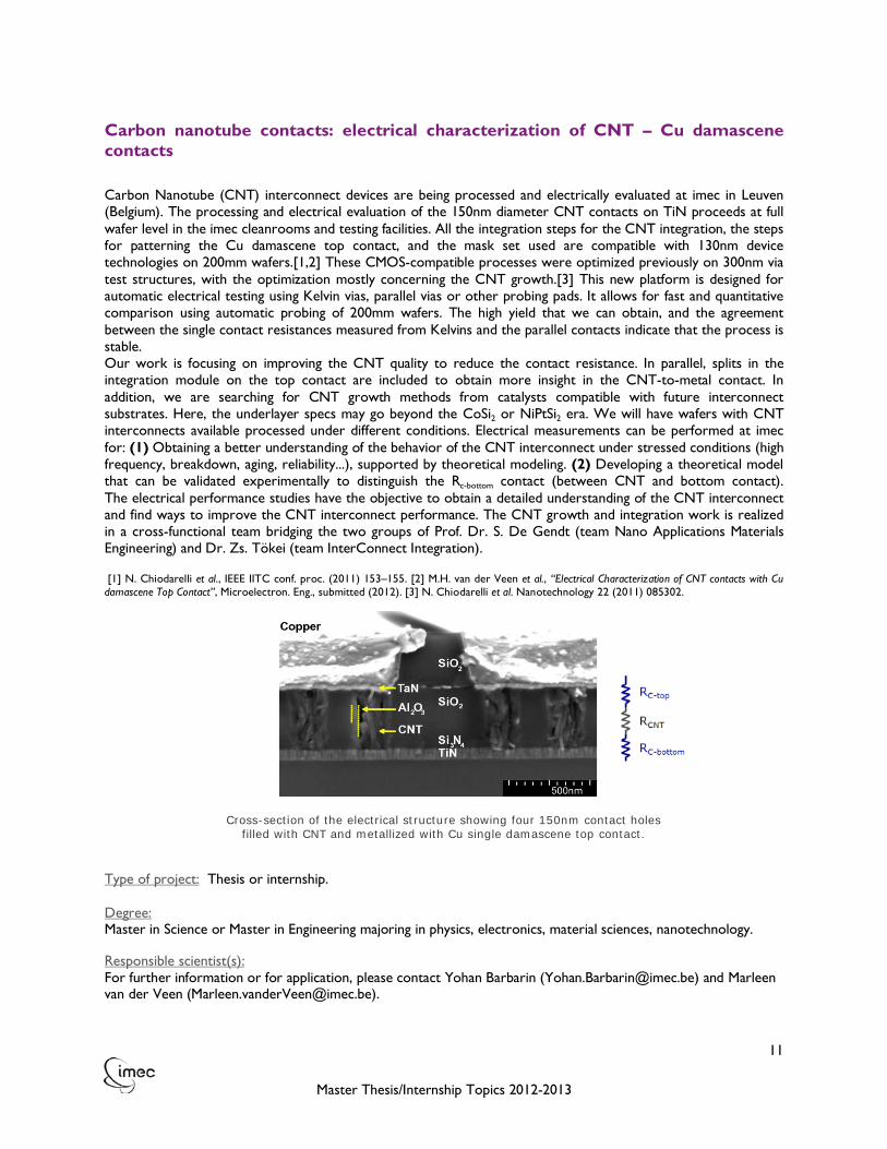
Carbon Nanotube (CNT) interconnect devices are being processed and electrically evaluated at imec in Leuven (Belgium). The processing and electrical evaluation of the 150nm diameter CNT contacts on TiN proceeds at full wafer level in the imec cleanrooms and testing facilities. All the integration steps for the CNT integration, the steps for patterning the Cu damascene top contact, and the mask set used are compatible with 130nm device technologies on 200mm wafers.[1,2] These CMOS-compatible processes were optimized previously on 300nm via test structures, with the optimization mostly concerning the CNT growth.[3] This new platform is designed for automatic electrical testing using Kelvin vias, parallel vias or other probing pads. It allows for fast and quantitative comparison using automatic probing of 200mm wafers. The high yield that we can obtain, and the agreement between the single contact resistances measured from Kelvins and the parallel contacts indicate that the process is stable. Our work is focusing on improving the CNT quality to reduce the contact resistance. In parallel, splits in the integration module on the top contact are included to obtain more insight in the CNT-to-metal contact. In addition, we are searching for CNT growth methods from catalysts compatible with future interconnect substrates. Here, the underlayer specs may go beyond the CoSi2 or NiPtSi2 era. We will have wafers with CNT interconnects available processed under different conditions. Electrical measurements can be performed at imec for: (1) Obtaining a better understanding of the behavior of the CNT interconnect under stressed conditions (high frequency, breakdown, aging, reliability...), supported by theoretical modeling. (2) Developing a theoretical model that can be validated experimentally to distinguish the Rc-bottom contact (between CNT and bottom contact). The electrical performance studies have the objective to obtain a detailed understanding of the CNT interconnect and find ways to improve the CNT interconnect performance. The CNT growth and integration work is realized in a cross-functional team bridging the two groups of Prof. Dr. S. De Gendt (team Nano Applications Materials Engineering) and Dr. Zs. Tökei (team InterConnect Integration).
[1] N. Chiodarelli et al., IEEE IITC conf. proc. (2011) 153–155. [2] M.H. van der Veen et al., “Electrical Characterization of CNT contacts with Cu damascene Top Contact”, Microelectron. Eng., submitted (2012). [3] N. Chiodarelli et al. Nanotechnology 22 (2011) 085302.
Cross-section of the electrical structure showing four 150nm contact holes
filled with CNT and metallized with Cu single damascene top contact.
Type of project: Thesis or internship. Degree: Master in Science or Master in Engineering majoring in physics, electronics, material sciences, nanotechnology.
Responsible scientist(s): For further information or for application, please contact Yohan Barbarin ([email protected]) and Marleen van der Veen ([email protected]).

12
Master Thesis/Internship Topics 2012-2013
Graphene synthesis and characterization
Graphene is a 2D, semi metallic, one-atom-thick sheet of sp2-bonded carbon atoms.[1] Graphene synthesis by means of mechanical exfoliation gives highest quality graphene but is not a CMOS compatible process due to (1) randomness of flake deposition (2) low yield. Growth on metal films (CVD graphene) or by annealing of SiC crystals (epitaxial graphene) still need high T budgets.[2] Although graphene is intrinsically compatible with CMOS processing because of its planar nature and transferability, technology will need a CMOS compatible synthesis method. Synthesis from solid carbon sources offers a clean method that is potentially compatible with front end of line processing, tools and scaling.[3]
The objective of this internship is to develop processes to synthesize graphene by means of anneal-type of solid stated reactions using SiC-based film stacks and by means of epitaxial growth from crystalline SiC. The candidate will also learn how to manipulate graphene in order to transfer it to alternate supports with the objective to fabricate and characterize devices.[4] Part of the work will entail the manipulation of graphene produced by mechanical exfoliation, for benchmarking purposes. The challenges involved are:
1. Fine tuning of process parameters to control the number of graphene layers grown. 2. Investigation of the influence of the substrate texture/crystallinity on the properties and quality of
synthesized graphene. 3. Study of the interfacial reactions between the substrate and graphene. 4. Post-processing of as-grown graphene (e.g., transfer, modification, device design).
The work will start from earlier findings within the graphene team[4] and is conducted in the group of Prof. Dr. S. De Gendt.
[1] Novoselov et al, Science 306 (2004) 666. [2] de Heer et al., Solid State Communications 143 (2007) 92. [3] Juang et al., Carbon 47 (2009) 2026. [4] Nourbakhsh et al, PSS 6 (2012) 53.
Type of project: Thesis or internship. Degree: Master in Science majoring in material sciences, nanotechnology, chemistry.
Responsible scientist(s): For further information or for application, please contact Marleen van der Veen ([email protected]) and Inge Asselberghs ([email protected]).

13
Master Thesis/Internship Topics 2012-2013
Atomic layer deposition for applications in nanotechnology
Atomic Layer Deposition (ALD) is an advanced technique to deposit thin films on a substrate from gas phase precursors. The film is deposited layer by layer through a cyclic process of self-limiting surface reactions. The use of self-limiting surface reactions results in a number of unique features, such as growth control at the atomic level and conformal deposition on extremely complex nanostructures.
Thanks to the process control at the atomic level, ALD has applications in nanotechnology. For example, the performance of computer chips and memory cells can be improved by introducing novel materials deposited by ALD, for example high-k dielectric oxides. A new potential application is energy storage in supercapacitors with nanostructured materials. ALD can also be used to increase the efficiency of solar cells, e.g. by introducing a passivation layer.
This thesis or internship topic frames in the research and development of ALD processes of metal oxides (e.g. Al2O3, HfO2, SrTiO3 , TiO2 …). The ALD process parameters need to be optimized in order to achieve uniform (nanometer thin) films with optimized properties. For example, the self-limiting aspect of the surface reactions is examined as it provides the basis for the process control at atomic level. The deposition temperature can affect the amount of impurities in the film and its phase. For deposition of metal oxides, the oxidant precursor (H2O, O3 …) also plays an important role. Insight in the surface chemistry (ligand exchange reactions or oxidation reactions) can provide a substantial contribution to the optimization of the process.
In order to characterize the nm-thin films, complementary measurement techniques are applied, such as spectroscopic ellipsometry, X-ray photoelectron spectroscopy, Secondary Ion Mass Spectroscopy…
Type of project: Thesis and/or internship of approx. 6 months. Degree: Master in Industrial Sciences or Master in Science or Master in Engineering majoring in chemistry, physics, material sciences.
Responsible scientist(s): For further information or for application, please contact Annelies Delabie ([email protected]) and Sven Van Elshocht ([email protected]).

14
Master Thesis/Internship Topics 2012-2013
XRD study of nano-structured hetero-epitaxial III-V compound semiconductors for VLSI CMOS applications
Since a few years, III-V compound semiconductors such as InGaAs, InP and InAlAs are being researched by the micro-electronics community as candidate materials for replacing silicon in the most advanced CMOS generations for 2020 and beyond. Due to the lattice mismatch and chemical differences, the epitaxial growth of these III-V materials on Si substrates requires specific approaches to control defect formation, which is lethal for highly performing circuits. Therefore, it is critically important being able to measure and analyze not only the thickness of these layers and their exact composition, but also such parameters as crystalline quality, defects and defect density. One of the most important techniques to assess the crystalline quality of semiconductor layers is X-ray diffraction, but in principle this technique is only applicable on bulk materials or blanket films. The purpose of this work is to develop measurement routines which allow to analyze nano-size structures by means of advanced XRD-tools, featuring thin film diffraction, grazing incidence X-ray diffraction, high-resolution X-ray diffration, X-ray pole figure analysis and/or X-ray rocking curve analysis.
Type of project: Thesis and/or internship. Degree: Master in Industrial Sciences or Master in Science or Master in Engineering majoring in material science, physics, electronics, ...
Responsible scientist(s): For further information or for application, please contact Clement Merckling ([email protected]) and Weiming Guo ([email protected]).
Developing in-situ doping of III-V compound semiconductors by hetero-epitaxial MOCVD growth
The epitaxial growth of III-V compound semiconductor on silicon substrate as channel material is a very promising method for future CMOS device fabrication because of their high electron mobility. Their implementation in conventional MOS structures requires thin III-V layers to be grown on a silicon substrate with shallow, abrupt and well-controlled doping profiles.. The doping efficiency is influenced by many growth conditions such as precursors, the growth temperature, annealing treatments etc. This work focuses on the doping of III-V thin layers (typically InGaAs, InAlAs) during MOCVD growth, by using different doping elements such as carbon and silicon. The aim is to develop effective and reproducible growth processes so that the doping concentration and diffusion of the doping elements can be tightly controlled.
Type of project: Thesis and/or internship. Degree: Master in Industrial Sciences or Master in Science or Master in Engineering majoring in material science, physics, electronics, ...
Responsible scientist(s): For further information or for application, please contact Clement Merckling ([email protected]) and Weiming Guo ([email protected]).

15
Master Thesis/Internship Topics 2012-2013
Surface preparation and interface passivation of high mobility channel materials for beyond 14 nm technology nodes
The continuous demand for downscaling pushes the Si transistor towards its physical limits. Therefore, new materials need to be introduced as channel materials. Possible candidates are SiGe, Ge, and III/V (e.g. InGaAs and InP). These materials exhibit high bulk mobilities. However, in order to fulfill their high expectations, the interface between the channel and the high-k needs to be passivated. Simply stated, a good passivation preserves the bulk properties throughout the interface between the channel material and the high-k oxide. In order to achieve this, we need to start from a defect free surface and the subsequent high-k deposition should not introduce new defects. Therefore, the first step is to control the surface chemistry of the channel material. This can be done by a wet chemical treatment or by a gas phase treatment prior to the high-k deposition. The goal is to study the resulting surface chemistry by highly advanced analysis techniques such as AR-XPS (Angle Resolved X-Ray Photo-electron Spectroscopy), TXRF (Total X-Ray Reflection Fluorescence), SIMS (Secondary Ion Mass Spectroscopy) ... . The next step is to study the influence of the surface chemistry on the high-k deposition by ALD (Atomic Layer Deposition) and hence the passivation of the interface created. Again, several analysis techniques need to be used in order to unravel the chemical bonding at the interface. Additionally, electrical characterization is needed to study the passivation of the interface formed. In the end, we need to come to a high quality interface with low defect densities in order to allow the introduction of these new materials in the next technology nodes.
Type of project: Thesis and/or internship. Degree: Master in Science or Master in Engineering majoring in chemistry, material sciences.
Responsible scientist(s): For further information or for application, please contact Sonja Sioncke ([email protected]).

16
Master Thesis/Internship Topics 2012-2013
Electrical evaluation and reliability assessment of local interconnects
In future CMOS technologies the individual transistors will be connected through local interconnects in order to increase the device density and to reduce the metal one complexity. These local interconnects however have to fulfill the same strict reliability specification as the other chip components and a thorough understanding of the potential degradation mechanisms is needed. The main aim of this thesis/internship is the electrical characterization of these local interconnects. This includes the evaluation of various newly designed test structures, the comparison of different local interconnect processes and the investigation of potential reliability issues.
Type of project: Thesis or internship of 6 months. Degree: Master in Industrial Sciences or Master in Science or Master in Engineering majoring in electronics.
Responsible scientist(s): For further information or for application, please contact Thomas Kauerauf (Thomas.Kauerauf @imec.be).
Investigation of advanced resistance-switching (RRAM) memory cells
Resistive Random-Access-Memory (RRAM), based on resistance switching mechanisms, is emerging as a potential nonvolatile memory candidate for below-20nm technology nodes, due to its better scalability, beyond the limits currently predicted for NAND Flash. 10nm-small RRAM cells are shown to have low voltage operation, very fast switching time, in the order of ns and below, small energy consumption per switching and good reliability. To take on the benefits of these excellent attributes to circuit level and enable high density memory array implementation, additional self-rectifying functionality is required for the resistive switching stack. The main task of this internship/thesis is to investigate RRAM cells that show self-rectifying characteristics, with the aim of understanding the switching behavior, relate it to intrinsic performance and identify paths for further improvement/optimization. You will be involved in electrical characterization, focusing on either performance or reliability aspects. You will be using state-of-the-art instrumentation and you will apply statistical principles in data collection using in-house developed characterization methodologies, so as to ensure a short response time in characterization. You will process data and assist in their interpretation. Feedback for process improvement is a key point. You must have a good background in semiconductor physics and knowledge of CMOS technology. You must be fluent in at least one programming/data analysis environment such as Matlab or similar and familiar with LabView and basic instrumentation for electrical testing. You will work in an international R&D team; a good command of English language is required. The detailed content of the work will be defined in detail at the moment of starting this project. Type of project: Thesis or internship of 4-6 months. Degree: Master in Science or Master in Engineering majoring in electronics, electrical engineering, physics.
Responsible scientist(s): For further information or for application, please contact Bogdan Govoreanu ([email protected]).

17
Master Thesis/Internship Topics 2012-2013
Investigation and optimization of the electrical switching properties of Conductive Bridging RAM memory cells (CBRAM)
The Resistance RAM is a new class of memories emerging as serious candidate for future memory replacement, in particular for high-density memory application. Resistance RAM cells typically consist of an insulator material sandwiched between two metal electrodes, and exhibiting resistive-switching properties, that is to say the application of an electrical current/voltage to the cell induces reversible changes of the cell resistance, which allows thus programming different memory states. The Conductive Bridging RAM (CBRAM) is a sub-class of RRAM, for which one of the electrode contains mobile elements (usually Cu or Ag) and which is based on the following switching mechanism: (1) applying a positive voltage to the Cu- or Ag-containing electrode activates the formation of a conductive bridge (or filament) in the insulator, resulting in the switching of the cell to a low resistance state (LRS); (2) on the other hand, a negative voltage activates the dissolution of this filament and thus the return to the high resistance state (HRS) (see Fig.1).
Fig1. Current-voltage switching traces and schematic of filament formation due to electrochemical dissolution and growth of the electrode metal element (from “R. Waser et al., Adv. Mater., 21, 2009”) At imec, we started a project aiming to develop Cu-based CBRAM cells. We fabricate cells consisting of different materials for the Cu-based electrode (pure Cu, or Cu-alloys) and for the insulator (binary oxides, nitrides, ...). The purpose of the thesis is to study the resistive-switching properties obtained for different stacks and to relate these switching characteristics to the physical properties of the used materials. The gained understanding of these relationships will allow to (1) better understand the switching mechanism, and (2) identify optimum material stack characteristics improving the memory parameters of the cell. To this aim the study will mainly consist in electrical measurements using conventional Current-Voltage measurements, as well as pulse-programming testing for scaled devices. Specific measurements like temperature-dependent I-V or impedance measurements may also be required. The study will be carried out within a project team consisting of experts in different fields (processing, integration, physical characterization, modeling ...), and in close collaboration with industrial partners. Type of project: Thesis or internship of minimum 5 months. Degree: Master in Science or Master in Engineering majoring in material sciences, physics, electronics.
Responsible scientist(s): For further information or for application, please contact Ludovic Goux ([email protected]).

18
Master Thesis/Internship Topics 2012-2013
Passivation of Ge for high-performance applications
Since several decades, the semiconductor material of interest to fabricate computer chips and other electronic devices has been Si. In the near future however, such high-performance applications may require a different type of semiconductor because Si does not fulfill the needs anymore. Due to its higher intrinsic carrier mobility and hence the possibility to operate at higher speed, Ge is being considered as a potential candidate to replace Si. A critical issue for the successful integration of Ge devices on the other hand is the electrical passivation of the Ge surface. This passivation is mandatory because defects like dangling bonds at the Ge/gate stack interface are able to trap charges and as such decrease the carrier mobility.
This thesis or internship topic frames in the research and development of an optimal passivation of the Ge surface, resulting in the highest feasible carrier mobility. We will focus on GeO2 as this type of passivation has shown to be promising. Also, the integration of GeO2 is quite straightforward since it can be obtained by oxidation of the Ge semiconductor surface. The quality of the GeO2 layer however will depend largely on the preparation method. Therefore, we will evaluate several techniques in order to obtain GeO2 of the best quality and a “defect-free” Ge/GeO2 interface. The physical quality of the GeO2 passivation layer will be examined by means of several measurement techniques like Spectroscopic Ellipsometry, X-Ray Photoelectron Spectroscopy and Atomic Force Microscopy. Capacitance-Voltage and Current-Voltage measurements will be applied for electrical evaluation. This electrical evaluation will first be done on capacitors, which consists of a Ge semiconductor substrate, a GeO2 passivation layer, a high-k dielectric layer and a metal gate. At the final stage, the passivation layer will be evaluated on transistors, resembling the eventual electronic device.
Type of project: Thesis and/or internship. Degree: Master in Industrial Sciences or Master in Science or Master in Engineering majoring in chemistry, physics, material sciences, electrical engineering.
Responsible scientist(s): For further information or for application, please contact Laura Nyns ([email protected]) and Sven Van Elshocht ([email protected]).

19
Master Thesis/Internship Topics 2012-2013
Graphene: device fabrication and characterization
Graphene, an atomically-thin sheet of carbon atoms arranged in a sp2 honeycomb lattice, has been successfully isolated for the first time only in 2004 [Novoselov et al, Science 306 (2004) 666.]. The peculiar electronic properties of graphene arise mainly from the configuration of its energy band structure, which, combined with the intrinsically low occurrence of defects and the stiffness of its lattice, allows for the featuring of intriguing 2-D physical phenomena. Graphene has been proposed as a candidate for CMOS and post-CMOS electronics. However, in order to make electronic applications of graphene realistic, one has to necessarily tune its electronic properties, so that, for example, a bandgap is introduced. The realization of a proper bandgap is critical for the device performance. Most recently, the research team has demonstrated the tuning of single-layer graphene by p- and n- doping due to engineering the interactions with the SiO2 support [Nourbakhsh et al, PSS 6 (2012) 53.].
Figure: (a) Transfer characteristics and (b) transconductance of SLG-FETs fabricated on pristine and silanized Si/SiO2 substrates. The latter sample is then treated in basic (red) and acidic (blue) solutions to turn the behavior from n- to p-type.[Figure taken from: Nourbakhsh et al, PSS 6 (2012) 53.] (c) image of a graphene device.
The candidate will learn how to manipulate and functionalize graphene, to characterize the doping level and the bandgap formation. Therefore, he/she will be involved in the design, fabrication, and characterization of graphene devices. Part of the work will entail the manipulation and functionalization of graphene produced by both mechanical exfoliation and synthetically grown graphene, for benchmarking purposes. The challenges involved are: • The study of the interfacial reactions between the substrate, graphene and doping layer; • Post-processing of as-grown graphene (e.g., transfer, modification, device design); • Device fabrication by lithography; • Electrical device characterization. The work will start from earlier findings within the graphene team and is conducted in the group of Prof. Dr. S. De Gendt.
Type of project: Thesis or internship. Degree: Master in Science or Master in Engineering majoring in material sciences, nanotechnology, chemistry, physics.
Responsible scientist(s): For further information or for application, please contact Inge Asselberghs ([email protected]).

20
Master Thesis/Internship Topics 2012-2013
Graphene: device fabrication for optoelectronics
Graphene, an atomically-thin sheet of carbon atoms arranged in a sp2 honeycomb lattice, has been successfully isolated for the first time only in 2004 [Novoselov et al, Science 306 (2004) 666.]. The peculiar electronic properties of graphene arise mainly from the configuration of its energy band structure, which, combined with the intrinsically low occurrence of defects and the stiffness of its lattice, allows for the featuring of intriguing 2-D physical phenomena. With respect to optoelectronic device performances, the high transparency in the visible-light range and the low resistivity of graphene sheets are the most attractive features, which makes graphene an ideal candidate to explore further its potential as a transparent electrode. The goal of this project is to study the layer interactions between substrate, graphene and optical active materials (e.g. quantum dot interactions), to characterize device performances and by molecular fine-tuning increase the optoelectronic device performance.
(a) (b) (c)
Figure: (a) Schematic of the QD-treated graphene transistor in the typical measurement configuration employed in this work. (b) Transfer characteristics Ids vs. Vg of a SLG FET in pristine conditions, after QD deposition, and during QD excitation (532 nm laser). The inset shows an optical microscope image of the 2-probe graphene device (scale bar: 2 μm). (c) Energy level diagram of the CdSe/ZnS QDs in contact with SLG.[Pictures taken from: Klekachev et al, Physica E: Low-dimensional Systems and Nanostructures (2011) 43(5) 1046-1049]
During the internship/master thesis you will learn how to manipulate and functionalize graphene, to characterize the doping level and the bandgap formation. Therefore, you will be involved in the design, fabrication, and characterization of graphene optoelectronic devices. The challenges involved are: • The study of the interfacial reactions between the substrate, graphene and doping layer; • Post-processing of as-grown graphene (e.g., transfer, modification, device design); • Device fabrication by lithography; • Electrical and optical device characterization The work will start from earlier findings within the graphene team and is conducted in the group of Prof. Dr. S. De Gendt.
Type of project: Thesis or internship. Degree: Master in Science or Master in Engineering majoring in material sciences, nanotechnology, chemistry, physics.
Responsible scientist(s): For further information or for application, please contact Inge Asselberghs ([email protected]) and Alexander Klekachev ([email protected]).

21
Master Thesis/Internship Topics 2012-2013
Characterization of ohmic contacts to high-mobility materials (Ge, III-V)
In near future, CMOS technology will have to implement novel semiconductors materials in the existing Si-based platform. This will allow maintaining good performances while scaling the CMOS features dimensions. High-mobility materials, like Ge and III/V compounds (GaAs, InGaAs, InAs...) are considered the best candidates to replace Si. In order to be able to implement these materials, contact schemes need to be developed to obtain low resistive ohmic contacts to Source and Drain areas of MOSFET devices. This needs also to be achieved working out integratable solutions. Fabrication and characterization (electrical and physical) of Metal/high-mobility materials test structures allows for extraction of specific contact resistivity values, which combined with thermal stability studies can lead to determination of proper contact scheme to satisfy ITRS requirements for sub-22 nm node. The candidate will start by studying the theory of ohmic contacts and metal/semiconductor systems. He/she will get familiar with state-of-the-art solutions for contacts on high mobility materials. He/she will follow closely the fabrication steps of test structures and perform electrical characterization, backing the results theoretical studies and simulations of Metal-Semiconductors systems.
Type of project: Internship or thesis with internship of 3-6 months. Degree: Master in Science or Master in Engineering majoring in physics, electronics, material sciences (focusing semiconductors materials). Responsible scientist(s): For further information or for application, please contact Andrea Firrincieli ([email protected]) and Jorge Kittl ([email protected]).

22
Master Thesis/Internship Topics 2012-2013
Spin transfer torque magnetic random access memory
As the demand for faster, smaller and more power-efficient devices is increasing, the present memory technologies, such as DRAM, SRAM, and NAND Flash are reaching their limits in terms of scalability beyond the 16-nm generation. Alongside the thriving effort to push further the boundaries of current technologies, new emerging memories have been developed and the spin-transfer torque magnetic random access memory (STT-MRAM) is considered the most promising replacement. This is the next generation of consumer mass-scale application of spintronics, following the widespread read head technology that hard drives use nowadays, which could open the way to a new era in which nano-spintronics complements or even replaces nano-electronics in a broad scale.
STT-MRAM is a type of non-volatile memory, it retains the information even when is not powered. It is based on magnetic materials, more specifically on magnetic tunnel junctions (MTJ), a sandwich composed of two ferromagnetic electrodes separated by an oxide barrier. The information in these devices is stored given the relative orientation of the ferromagnetic layers. A high resistive state is found when they are antiparallel and a low resistive state when both ferromagnets are pointing towards the same direction. The control of the magnetization is done via the spin-transfer torque effect (STT) that enables to manipulate magnetizations by applying electrical currents that become spin-polarized when traveling through the ferromagnets.
Imec is implementing a very exciting and challenging program on the development of STT-MRAM devices on the 300-mm platform, aiming ultrafast devices at the smallest possible technology nodes.
Several possibilities for master thesis and internships are possible. Experimental studies will be carried out on the magnetic properties of novel materials with perpendicular magnetic anisotropy. This will be carried out via combinatorial sputtering deposition (outsourced), electrical (transport) and optical (MOKE) characterizations. To support the experimental findings, micromagnetic simulations will be investigated on distinct properties. For example, to predict the magnetization behavior during the write process is crucial to reduce the necessary write current. This reduction in current also depends on the optimization of key parameters such as magnetic damping and anisotropy energies.
Knowledge on magnetism is an asset.
Type of project: Thesis and/or internship. Degree: Master in Science or Master in Engineering majoring in material sciences, physics.
Responsible scientist(s): For further information or for application, please contact Mauricio Manfrini ([email protected]), Sven Cornelissen ([email protected]) and Jorge Kittl ([email protected]).

23
Master Thesis/Internship Topics 2012-2013
Wet processing of high aspect ratio nanostructures
In semiconductor manufacturing, two critical issues in the wet processing of nanostructures with high aspect ratio are incomplete wetting and pattern collapse. The contact angle that a liquid drop makes with an ideally flat surface depends mainly on surface chemistry. Amplification of hydrophobicity by surface patterns is frequently seen in nature (e.g. so-called lotus effect) and is illustrated in Figure 1 for flat and nano-patterned silicon surfaces. Development of superhydrophobic behavior can lead to processing defects from incomplete wetting in between nanostructures. On the other hand, as the critical dimensions of structures scale down, capillary force can cause significant deflection of high aspect ratio structures and pattern collapse can occur after complete drying. Figure 2 shows the SEM images of free standing nano pillars before a wet treatment (a), and self organized patterns formed after pillars are brought together by capillary forces (b & c). These pattern collapses should be prevented in industrial fabrications.
In this project we investigate the wetting behavior of solutions on nanostructures with different surface chemistries and the parametric dependence of pattern collapse on the wetting properties of the structure material as well as structure dimensions. The student will have access to imec’s state-of-the-art cleanroom facilities and get hands on experience of contact angle measurement, Fourrier transform infra-red spectroscopy (FTIR), electroless metal deposition and surface modification by adsorption.
(mirror image)
Figure 1. Water droplets on flat (left) and nano-patterned (right) silicon surfaces.
(a) (b) (c)
Figure 2. Top-down SEM images of (a) free standing pillar structures with high aspect ratio; (b) and (c) self-organized collapsing patterns formed after a wet processing.
Type of project: Thesis or internship of minimum 3 months. Degree: Master in Industrial Sciences or Master in Science or Master in Engineering majoring in material sciences, chemistry, physico-chemistry.
Responsible scientist(s): For further information or for application, please contact Guy Vereecke ([email protected]) and XiuMei Xu ([email protected]).

24
Master Thesis/Internship Topics 2012-2013
Surface chemistry of III-V semiconductors for cleaning applications
In order to meet the future demands imposed by the scaling roadmap, the heart of the transistor, the channel, needs to be replaced by a new material in which the mobility of the charge carriers is higher than for silicon. Semiconductor compounds based on group III and V elements of the periodic system e.g. InP and InGaAS meet these requirements. The III-V materials are grown in transistor structures through the gas phase with epitaxial and atomic layer deposition techniques. A critical factor controlling deposition is the starting condition of the surface as this influences the nucleation and properties of the grown layer. When contamination is present in the form of native oxides, metals and particles, or when dangling bonds are not fully passivated, defects will be introduced in the deposited layer or at the interface. Such defects are usually electronically active and reduce the efficiency of the transistor. Minimizing defect densities in transistor structures is essential and can be achieved with controlled chemical surface treatments. In order to design wet chemical solutions that lead to an appropriate surface pre-conditioning and allow for nano-scale processing of these III-V materials, a thorough understanding of the interactions between the substrate and the chemical solutions is needed and the basic etching mechanism needs to be investigated on a (sub) nanometer level.
The goal of this project is to find a suitable chemistry which leads to selective contaminant removal and controlled etching of the substrate in order to guarantee removal of surface defects in the crystal lattice. This (sub)nanometer etching should be independent of crystal orientation in order to keep the surface stoichiometry intact. After contamination and defect removal reoxidation of the surface poses a problem and can be minimized by sulfur based passivation. At present we are screening various sulfur chemistries and we are characterizing the passivation process. For this research the following techniques are important: • ICP-MS to determine the amount of dissolved III-V material (ppb-ppt level) • TXRF to measure metallic contamination on III-V surfaces • Electrochemistry to study kinetics of etching and metal deposition • Photoluminescence to obtain insight in surface passivation and defect levels • XPS to measure surface composition • Atomic Force Microscopy to measure surface roughening at the atomic scale.
We are looking for enthusiastic and motivated students majoring in chemistry, material sciences or related field with a strong interest in chemistry/physics of semiconductors and analytical chemistry. The duration of this project is 2-12 months (assuming full time presence).
Type of project: Internship with thesis (2-12 months full-time). Degree: Master students majoring in chemistry, material sciences.
Responsible scientist(s): For further information or for application, please contact Dennis van Dorp ([email protected]).

25
Master Thesis/Internship Topics 2012-2013
The creation of nanoforces by microbubbles
Bubbles can be created in fluids and are used for a broad range of applications. Under the influence of pressure variations, bubbles can implode which is shown in figure 1. The last few years, the research in microbubbles has been ramped up, because imploding microbubbles can be used in biomedical applications. An example is the implosion of microbubbles near a cancer cell, which result in the perforation of the cell membrane. Once the cell membrane is open, the injection of medicine is facilitated. The ruptured membrane of living cells usually heals within a time span of a few minutes. An example of a ruptured cell is shown in figure 2. In the semiconductor industry, oscillating bubbles are used to remove contaminants or nanoparticles from fragile structures. By using
ultrasound or, in other words, the same sound field for visualizing fetuses, small bubbles can be created. These microbubbles oscillate with the same rhythm as the sound field. If the sound pressure is high enough, the bubbles will oscillate very strong and they can even collapse. Such a collapsing bubble will remove nanoparticles from a surface. Currently the implosion is not very well controlled and also results in damaged fragile structures. More in depth research is necessary to control the nanoforces created by the imploding microbubbles. The final goal of the work is to control the microbubble size and to facilitate bubble nucleation. Several aspects need to be investigated, including the effect of charge, surface tension, spatial distribution of microbubbles, changes in the sound field... The experimental tools which can be used for this type of work are sonoluminescence tests, cavitation noise measurements, damage and particle removal tests... The latter experiments are closely related with the practical cleaning process. Nanoparticles will be deposited on a surface in a controlled way, which will be measured with light scattering techniques. Next, these particles will have to be removed with the microbubbles that are created during the application of ultrasound. During an intensive training period, the student will learn how to operate the tools and interpret results. Type of project: Thesis of minimum 4 months (full-time) and maximum 1 year. Degree: Master in Science or Master in Engineering majoring in physics, chemistry, material sciences.
Responsible scientist(s): For further information or for application, please contact Steven Brems ([email protected]).
Figure 2 Cell ruptured by an imploding bubble
Figure 1 Implosion of a bubble

26
Master Thesis/Internship Topics 2012-2013
Galvanic corrosion in micro-bump with different bumping metallurgy
The electronics industry is increasingly looking into 3D integration in order to address the ever continuing product needs of miniaturization and performance increase for future generation of ICs. This result in high speed interconnects with reduced noise and crosstalk as compared to wire bonded assemblies. 3D integration requires a physical stacking such as die to die (D2D) or die to wafer (D2W) while forming a permanent electrical and mechanical connection between the input/output pins of the devices. Fine pitch micro-bump connection is considered as a promising approach for making die to die interconnections due to its lower bonding temperature. A micro-bump consists of a solder bump and an Under-Bump-Metallisation (UBM) on the die. The reaction between solder and UBM results in intermetallic formation and hence the top and bottom dies are connected. This UBM must meet several requirements. First it must provide a strong, stable, low resistance electrical connection to the underlying metal such as aluminum and Cu. Then it must adhere well both to the underlying metal and to the surrounding IC passivation layer. The UBM must also provide a strong barrier to prevent the diffusion of other bump metals into the IC. Finally the UBM must be readily wettable by the bump metals, for soldering.
Continuous downscaling in the micro-bump pitch requires new materials to meet all the afro-mentioned requirements. However, the compatibility between the new material and the existing technology needs to be evaluated.
For this specific topic the applicant would be required to investigate galvanic corrosion in multi-layer UBM system. He will be also asked to investigate polarization behavior of different metals in a few Cu etchants and study the galvanic corrosion tendency based on experiments. Moreover, he is asked to integrate the possible solutions to reduce galvanic corrosion. Finally, the impact of galvanic corrosion on 3D chip stacking and electrical performance such as electro-migration, thermal cycling and high temperature storage will be evaluated. He should be able to execute appropriate DoEs under the guide of his mentor. During the execution phase he will be supported by imec experts and allowed to use imec advanced facility.
Type of project: Thesis with internship of 6 months-1 year. Degree: Master in Science or Master in Engineering majoring in chemistry (preferred), material sciences, physics, electronics. Responsible scientist(s): For further information or for application, please contact Wenqi Zhang ([email protected]) and Philippe Vereecken ([email protected]).

27
Master Thesis/Internship Topics 2012-2013
Direct heteroepitaxy of III-V semiconductors on silicon mediated by strain-relaxed buffer layers
High mobility III-V semiconductors are an increasingly hot topic of research in the semiconductor industry. Their use for high performance, low power logic devices has been envisioned, in the International Technology Roadmap of Semiconductors (ITRS), for the 11-nm node and beyond. So far, the growth of III-V structures has been almost exclusively carried out on lattice-matched III-V substrates (i.e. In53%GaAs or In52%AlAs lattice-matched to InP substrates), to ensure that a defect-free, device-quality III-V active layer is achieved. The monolithic integration of III-V materials onto a Si-based platform would bring a number of advantages: no need for large-size, expensive III-V substrates; CMOS compatible processing; possibility to integrate different functional blocks monolithically onto the same Si platform, such as logic/switching circuitry, high-frequency circuitry, and even optical interconnects. However, the challenge of monolithic III-V integration onto Si poses tremendous challenges both at the processing/integration level, and at a more fundamental material level.
The latter aspect arises from the considerable difference in lattice mismatch between Si and some of the III-V materials considered as candidates for III-V high mobility channels (e.g. a formidable 8% between Si and In53%GaAs). The lattice mismatch makes it difficult to achieve the growth of a defect-free III-V epitaxial layer directly on Si. Additionally, the generation of polar/non-polar interfaces between a group-IV semiconductor (Si) and a III-V material can result in the formation of antiphase boundaries (APBs), considered detrimental for correct device operation. In order to mitigate the issues aforementioned, one of the approaches currently evaluated by the scientific and industrial community entails the growth of a Strain Relaxed Buffer (SRB) between the Si substrate and the III-V device layer. Data show that this route allows for a drastic reduction of the number of defects reaching the active III-V device layers.
The project focus is to investigate the SRB structure dependence on a number of process parameters. The structures will be grown by Metal-Organic Chemical Vapor Deposition (MOCVD). Concurrently, the candidate is expected to characterize the stacks grown, both structurally (X-ray diffraction, electron and optical microscopy) and electrically (Hall and sheet resistivity measurements on the active device layer). The candidate should also be able to interpret the data collected and extract meaningful correlations.
Type of project: Internship of minimum 3 months. Degree: Master in Industrial Sciences or Master in Science or Master in Engineering majoring in material sciences. Responsible scientist(s): For further information or for application, please contact Mirco Cantoro ([email protected]).

28
Master Thesis/Internship Topics 2012-2013
3D FIB/SEM structural analysis of nano-electronic devices
Cross-sectional structural analysis of devices is important to control and optimize the processing, e.g. by measuring layer thickness, etch depth and profile, trench filling or contact morphology. The combination of focused ion beam milling (FIB) with scanning electron microscopy (SEM) in a “dual-beam FIB/SEM” is a major metrology tool for these applications. To cross the point of interest, generally a manual sequential slice (i.e. ion beam milling) and view (SEM image) approach is needed.
Topic for the internship is to investigate the use of automated slice and view routines for application to small device structures as well as large volumes. Based on the obtained set of images a 3D reconstruction of the device volume can be made with dedicated software. Subsequently this can be cut in any given direction. With the electron and ion beam conditions the information depth in the images and the step between the subsequent slices can be varied. The combination of both will determine the resolution of the 3rd dimension in the reconstructed volume.
The work will involve: get acquainted to acquire high-quality SEM images, to explore the capabilities of the automated slice-and-view image acquisition software and to establish best procedures for small or very large volumes, to study the best experimental conditions for the milling and imaging, and 3D reconstruction of the set of images. Applications will be e.g. metallization structures on devices, through-silicon-vias (TSV), neuron cells on nano-devices.
Type of project: Internship of 3-6 months. Degree: Master in Industrial Sciences or Master in Science or Master in Engineering majoring in material sciences, physics, electronics. Responsible scientist(s): For further information or for application, please contact Hugo Bender ([email protected]).

29
Master Thesis/Internship Topics 2012-2013
Carrier depth profiling with micro-probes on advanced ultra-shallow high-mobility CMOS semiconductor structures
As CMOS devices get smaller with each technology node, the processes needed to fabricate and characterize these also become more and more complex. Moreover, the fast introduction of new high mobility materials (Ge, III-V) additionally complicates the electrical analysis of these new structures. Crucial technological parameters which directly relate to the performance of the final devices are the sheet resistance of the involved ultra-shallow junctions (USJ’s) and the detailed shape of their carrier depth profile.
Historically conventional four-point probes (with mm separation and 100 g load) have been used (and still are) for the determination of the sheet resistance. The Spreading Resistance Probe (SRP) has been used for carrier depth profiling of USJ’s on Silicon and Germanium and Electrochemical Capacitance Voltage on III-V materials. As new high mobility materials are, however, introduced and USJ become shallower (sub-50 nm), these conventional tools become basically useless (too high probe penetration, too large contacts, large correction factors, insufficient depth control, etc.).
Recently two promising new tools have become available, i.e. the micro-four point probe (M4PP) and the NanoProber (NP). The main strength of the former is accurate, absolute, zero-penetration, sheet resistance measurement (within 0.1%), the strength of the latter is measurements in vacuum with highly flexible positioning of the micro-probes. Both tools can be applied to the new high-mobility materials needed today and have probe contact sizes small enough for sub-50 nm depth profiling. The main goal of this work is to investigate and compare in detail the two- (=spreading resistance) and four-point (=sheet resistance) based capabilities of M4PP and NP to accurately extract carrier profiles along a slanted (beveled) surface for sub-50 nm ultra-shallow junctions in high mobility materials and to develop a physical understanding for the observed differences (noise behavior, shape calibration curves, sampling volume, etc.).
The major steps in this work will be: (i) Familiarizing oneself with all the tools involved in this work (M4PP, NP (+SEM), profilometers, polishing tools, Labview and Tivoli software, etc.), (ii) Enhancing the NP software to allow for two (four) point resistance depth profiling, (iii) Performing M4PP and NP measurements (iv) Investigate the impact of different measurement parameters (pitch, pressure) on the accuracy of the extracted carrier profiles, (v) Developing physical understanding for the observed experimental results, (vi) comparing results with other techniques such as Scanning Spreading Resistance Microscopy (SSRM), SRP and Secondary |Ion mass Spectrometry (SIMS) data.
Type of project: Thesis of 6 months. Degree: Master in Science or Master in Engineering majoring in physics, electrical/electronic engineering, material science. Responsible scientist(s): For further information or for application, please contact Trudo Clarysse ([email protected]) and Kai Arstila ([email protected]).

30
Master Thesis/Internship Topics 2012-2013
Development of a professional data analysis package for the micro-four point probe (M4PP)
The micro-four point probe (M4PP) is an electrical technique that allows for the very accurate measurement of the (sheet) resistance of a very thin (sub-100 nm) highly conductive semiconductor layer on top of a substrate of opposite impurity type (n- or p-type) (by pushing a current through the outer two probes and measuring the resulting voltage difference between the inner two probes). In 2009 such a M4PP tool has been installed at imec. The tool came with commercial software (from Denmark) for the sheet resistance raw data collection, but not for the data manipulation of the many different data files or consequent data interpretation.
When applying this technique to a bevelled surface (slanted), one can generate a sheet resistance versus depth profile, from which the underlying carrier depth profile can be extracted. The latter is of crucial importance for the development of future state-of-the art transistors. In 2010-2011 an initial version of a brand new M4PP data treatment software package named “Tivoli” has been implemented. During the next (second) academic year Tivoli was enhanced among others with improved smoothing capabilities, a graphics overlay module and printing capability.
The goal of the third working year of this project is, to continue the development of the Tivoli package for both surface sheet resistance+mobility and carrier depth profiling analysis. The programming environment is Microsoft Visual C++, with the Trolltech/Nokia Qt4 class libraries and Qwt graphics libraries. Issues involved in this work will be: (i) For surface analysis, making different types of result plots/maps (resistance/voltage versus position, two-dimensional 200- and 300 mm resistance contour maps, etc.) and implementing support for a new micro-probe CIPTech tool allowing to extract mobility data from the measurements, (ii) For carrier depth profiling, implementing probe pitch correction algorithms and adding support for two point (so called spreading resistance) measurements, which have a smaller sampling volume, (iii) Adding further support for making overlays with profiles from other dopant and carrier characterization techniques, (iv) Eventually semi-automatically generation of analysis results reports (in MS Word or PDF format).
It is not the aim of this work to develop new data treatment “algorithms’. This subject is, however, a challenge for those who wish to specialise themselves in all aspects and capabilities of object-oriented Windows programming within the Visual C++ environment with a signal-slot architecture (Qt) environment, focussing on a truly user-friendly graphical user interface (GUI).
Type of project: Thesis of 6 months. Degree: Master in Industrial Sciences majoring in electrical/electronic engineering, option information- and communication techniques (ICT). Responsible scientist(s): For further information or for application, please contact Trudo Clarysse ([email protected]).

31
Master Thesis/Internship Topics 2012-2013
Development of an industrial analysis-package in Visual C++ for SSRM-measurements
The goal of this project is to develop and to implement in the Microsoft Visual Studio C++ 2008 (v9) programming environment in combination with the Microsoft Foundation Class (MFC) libraries, Windows XP/Vista/7 compatible software for the analysis of SSRM-measurements, which has been named MicroQuanti (MQ). This thesis is part of a long-term project.
Figure 1. Screenshot of the MicroQuanti software illustrating the area detection and the quantification procedures for a classical planar MOSFET. SSRM (Scanning Spreading Resistance Microscopy) is an AFM (Atomic Force Microscopy) based technique developed a few years ago that makes use of a very small conducting probe (nm scale) to measure the local resistance of a small piece of conducting material along its cross-section. This delivers a two-dimensional resistance image where the colour of every pixel is corresponding to the magnitude for the measured resistance (see Figure1). The SSRM resistance picture has then to be converted as accurately as possible into a carrier concentration image where every pixel indicates the number of carriers (electrons and/or holes) present at every position. The aspects that will be investigated in this thesis are the improvement of the two-dimensional smoothing procedure for the resistance pictures (suppression of noise in the measurements) and the introduction of a two-dimensional quantification procedure based on a new type of calibration structure (from resistance to carrier concentration). Furthermore, a new graphics user interface will have to be developed to allow the end-user more control over a large number of critical parameters. Type of project: Thesis of 6 months. Degree: Master in Industrial Sciences majoring in electrical/electronic engineering, option information- and communication techniques (ICT). Responsible scientist(s): For further information or for application, please contact Trudo Clarysse ([email protected]) and Pierre Eyben ([email protected]).

32
Master Thesis/Internship Topics 2012-2013
Development of probes for nanoscale electrical measurements and manipulation in a nanoprober system
Imec’s nanoprober consists of an electron microscopy (SEM) system which is equipped with up to four nanomanipulators and electrical measurements units. It allows for dedicated nanoscale manipulation, measurement and characterization tasks. Various add-on components have been added to the nanoprober such as an energy dispersive X-ray spectroscopy (EDS) unit, a heating stage, a micro-gripper, an electron beam induced current (EBIC) module, and a micro-gripper which are extending the application range. It is used for example for electrically probing nanostructures such as nanowires and carbon nanotubes, for characterizing localized thin-film stacks, and for manipulating nanostructures using a pick-and-place approach.
Electro-chemically etched tungsten wire needles are commonly used as tips in the nanoprober. They are manually made and suffer from oxidation and suffer from low sharpness of typically 50-100 nm. Furthermore, tungsten is not well suited for all measurements and alternative tip materials are highly desirable. Therefore, we have demonstrated in a first step micro-fabricated in-plane diamond tips and evaluated them in the nanoprober. Besides their in-plane tip geometry, the probes are similar to common scanning probes used in atomic force microscopy (AFM). Unfortunately, this probe configuration is too cumbersome to use in a nanoprober setup. It is therefore the aim of this internship to develop and test a dedicated probe configuration for the nanoprober. For this, micro-fabricated tips in metal and doped diamond will be assembled to dedicated nanoprober probes and will be then mechanically and electrically evaluated inside the nanoprober. The student will optimize the probe assembly and configuration. He/she will learn to work with SEM, to carry out micro-assembly, and to manipulate and electrically measure on the nanometer scale.
Type of project: Internship of 3-6 months. Degree: Master in Industrial Sciences or Master in Science or Master in Engineering majoring in material sciences, physics, electrical engineering, ... Responsible scientist(s): For further information or for application, please contact Thomas Hantschel ([email protected]).

33
Master Thesis/Internship Topics 2012-2013
Diamond probes – more efficient and optimized yield assessment
Boron-doped diamond tips have become the ultimate choice for performing electrical measurements on the nanometer scale with ultra-high spatial resolution. In contrast to other diamond applications where it faces a strong competition from other materials, doped diamond is the only material which can withstand the extremely high pressures (in the GPa range) needed to establish a good electrical contact on silicon and germanium. The solid diamond tips are made by so-called molding whereby first a pyramidal pit is etched, then it is filled up with diamond and finally the mold is etched away. The pyramidal tip is attached to the end of a metal cantilever beam. Using such probes advanced nanoelectronics device structures (e.g. planar field-effect transistors (FETs), FinFETs, tunnel-FETs (TFETs), solar cell structures) are routinely measured in scanning spreading resistance microscopy (SSRM) with a spatial resolution of ≤1 nm. However, the fabrication yield for such tips is still very limited to only about 30-50%. A tedious and time consuming probe evaluation procedure is therefore in place to determine the yield for a fabricated probe wafer (~45 minutes per probe, ~15 hours per wafer). The measurements results are important feedback for further process optimization. Another drawback of the existing evaluation procedure is that there is an observation gap between the tests done on the calibration structures and on real-life device structures. The goal of this internship is therefore the development of an improved probe qualification methodology. This involves the critical assessment of the existing testing procedure with respect on how it can be improved towards a better match with device measurement observations and the reduction of probe testing per probe and wafer respectively. For this, also more advanced calibration structures will be studied and novel approaches for probe yield determination will be assessed. The student will be trained in the use of atomic force microscopy (AFM), in particular the use of the SSRM method. He/she will learn and carry out probe mounting and testing of in-house fabricated full-diamond tips. After having gained practical experience in the use of the existing methodologies, the student will work towards a more efficient and predicting probe qualification process. Type of project: Internship of 6 months. Degree: Master in Industrial Sciences or Master in Science or Master in Engineering majoring in material sciences, physics, electrical engineering, ... Responsible scientist(s): For further information or for application, please contact Thomas Hantschel ([email protected]).
34
Master Thesis/Internship Topics 2012-2013
Advanced materials characterization using ion beam scattering
This topic is an opportunity to learn about fundamental materials characterization techniques in a state-of-the-art nanoelectronics research center. You will be exposed to challenges in current and future CMOS technology.
Novel materials processing techniques and characterization approaches have boosted the nanoelectronics industry dramatically. We have witnessed the introduction of high-k materials (e.g. HfO2) replacing the SiO2 insulator in advanced transistors, and metals (e.g. TiN) replacing poly-Si as a gate material. Yet, the introduction of novel materials is expected to be even more essential in the future. Research is ongoing to replace Si by alternative materials that exhibit a higher mobility. Finally, new materials are also needed for the realization and optimization of new devices such as resistive memory (RRAM) cells, conductive bridge resistive memory (CBRAM), photovoltaic (PV) cells, nano-batteries, micro-electromechanical systems (MEMS), light emitting diodes (LEDs) etc.
The development of new materials at imec builds also upon the experience and expertise of the materials and component analysis (MCA) department.
One of our major tools is an ion accelerator (maximum 2 Mega Volt) with two dedicated end stations; one for Rutherford Backscattering spectrometry (RBS), and another for Elastic Recoil Detection (ERD) experiments. In RBS, essential information from the sample is gained from the residual energy of the scattered projectiles. In ERD, the information comes from the energy of the recoiled target atoms. To attain the best possible detection resolution, the acceleration voltage and the projectile species need to be properly chosen in relation with the nominal sample structure and the known detection schemes.
The focus of your work will be to investigate novel materials, e.g. GaN, using Elastic Recoil Detection experiments. Till now, at imec, we have been employing mostly a 6 MeV Cl beam for the ERD analysis of thin films. It may be expected that projectile beams other than Cl (e.g. Cu, Br, I) and primary energy other than 6 MeV are more effective in the analysis of certain thin films. Through simulations (software available) and practical experiments, you will investigate the capabilities of various ion species and acceleration voltages towards the analysis of new materials.
Type of project: Internship or thesis of 6 months. Degree: Master in Science or Master in Engineering majoring in material sciences, physics, chemistry, electronics. Responsible scientist(s): For further information or for application, please contact Johan Meersschaut ([email protected]).
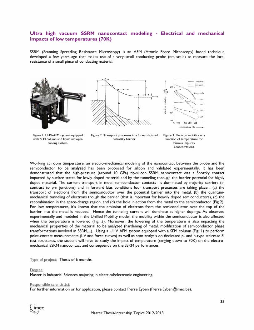
35
Master Thesis/Internship Topics 2012-2013
Ultra high vacuum SSRM nanocontact modeling - Electrical and mechanical impacts of low temperatures (70K)
SSRM (Scanning Spreading Resistance Microscopy) is an AFM (Atomic Force Microscopy) based technique developed a few years ago that makes use of a very small conducting probe (nm scale) to measure the local resistance of a small piece of conducting material.
Figure 1. UHV-AFM system equipped with SEM column and liquid nitrogen
cooling system.
Figure 2. Transport processes in a forward-biased Schottky barrier
Figure 3. Electron mobility as a function of temperature for
various impurity concentrations
Working at room temperature, an electro-mechanical modeling of the nanocontact between the probe and the semiconductor to be analyzed has been proposed for silicon and validated experimentally. It has been demonstrated that the high-pressure (around 10 GPa) tip-silicon SSRM nanocontact was a Shottky contact impacted by surface states for lowly doped material and by the tunneling through the barrier potential for highly doped material. The current transport in metal-semiconductor contacts is dominated by majority carriers (in contrast to p-n junctions) and in forward bias conditions four transport processes are taking place : (a) the transport of electrons from the semiconductor over the potential barrier into the metal, (b) the quantum-mechanical tunneling of electrons trough the barrier (that is important for heavily doped semiconductors), (c) the recombination in the space-charge region, and (d) the hole injection from the metal to the semiconductor (Fig 2). For low temperatures, it’s known that the emission of electrons from the semiconductor over the top of the barrier into the metal is reduced. Hence the tunneling current will dominate at higher dopings. As observed experimentally and modeled in the Unified Mobility model, the mobility within the semiconductor is also affected when the temperature is lowered (Fig. 3). Moreover, the lowering of the temperature is also impacting the mechanical properties of the material to be analyzed (hardening of metal, modification of semiconductor phase transformations involved in SSRM,...). Using a UHV AFM system equipped with a SEM column (Fig. 1) to perform point-contact measurements (I-V and force curves) as well as scan analysis on dedicated p- and n-type staircase Si test-structures, the student will have to study the impact of temperature (ranging down to 70K) on the electro-mechanical SSRM nanocontact and consequently on the SSRM performances.
Type of project: Thesis of 6 months. Degree: Master in Industrial Sciences majoring in electrical/electronic engineering. Responsible scientist(s): For further information or for application, please contact Pierre Eyben ([email protected]).

36
Master Thesis/Internship Topics 2012-2013
Atomic Layer Deposition of ultrathin metal films for advanced nanoelectronic applications
Ultrathin metal films play an increasingly important role in advanced microelectronics, e.g. as gate electrodes in transistors and capacitors and as diffusion barriers and seed layers in interconnect applications. For dielectric thin films, the most customary deposition method is atomic-layer deposition (ALD) because of the possibility of depositing high-quality films at low temperature. By contrast, the deposition of metallic thin films by ALD has been studied much less. Recently, there is high interest in the ALD of elementary metals such as ruthenium, aluminum, tantalum... .
The ALD of metals encounters several challenges. First, a very long growth inhibition is often observed, i.e. the deposition starts only after a certain time span, during which the surface is exposed to the precursors but no film is deposited. The growth inhibition often implies a rough, island-like film growth. That is highly unwanted because for all applications, ultrathin (< 5 nm), smooth and continuous metal films are required. Second, in many cases of metal ALD, plasma is used during the ALD process. The latter is called plasma-enhanced ALD (PE-ALD). PE-ALD often results in improved growth and better properties of the deposited metal, such as conductivity, purity. However, the plasma however, can also detrimentally impact the substrates properties due to exposure of the substrates’ surface to the plasma species at the initial stage of the growth.
The student will conduct experiments on state-of-the-art (PE)-ALD equipment in order to deposit ultra-thin, continuous metal films. The focus will be on the understanding and characterization of the initial growth of the films with the aim to improve the nucleation and the film properties. To study the film properties, he will use various techniques such as ellipsometry, X-ray-reflectivity and -diffraction measurements, resistivity by 4-points probe measurements, rutherford backscattering spectrometry,... Furthermore, he will be involved in the integration of the deposited layers in nanoelectronic devices to assess its impact on device level.
Type of project: Thesis and/or internship. Degree: Master in Industrial Sciences or Master in Science or Master in Engineering majoring in physics, chemistry, material sciences.
Responsible scientist(s): For further information or for application, please contact Johan Swerts ([email protected]) and Sven Van Elshocht ([email protected]).

37
Master Thesis/Internship Topics 2012-2013
In-situ molecular beam passivation of III-Sb compounds
Further scaling of CMOS High Performance devices and circuits for logic applications along the lTRS roadmap guidelines asks more and more for high carrier mobility channel materials. The antimonide-based III/V’s are known to have even higher mobilities, up to 77000 cm2/V.s for InSb. The most exciting aspect of the III/Vs however could be that also pFETs could become in reach if we look into strained antimonides, with mobilities even higher than these of germanium. Two major problems with antimonides is i) how to fabricate these materials on our standard large size silicon substrates, and ii) how to passivate the gate oxide/channel interface. With respect to the first problem, the most straightforward solution is to grow these materials on the silicon substrate. Two issues have to be taken into account, which is the huge difference in lattice size (almost 16 % for InSb), and the strong tendency to segregation and facet formation. Concerning the second problem: in order to suppress gate leakage, one has to make use of a thin high-k dielectric layer between the channel and the metal gate. But passivation of this interface between the compound semiconductor and a high-k dielectric is known to be a huge problem. In this context, an appropriate passivation techniques have to be developed (in-situ oxide deposition, H2S-H2Se interlayers, ...), keeping in mind that the equivalent oxide thickness (EOT) must be controlled down to ~0.5 nm.
The purpose of this work is to study physically and electrically the in-situ passivation of III-Sb semiconductors with different passivation schemes and high-k oxide by the means of molecular beam epitaxy techniques.
Type of project: Thesis and/or internship. Degree: Master in Industrial Sciences or Master in Science or Master in Engineering majoring in material science, physics, electronics, ... Responsible scientist(s): For further information or for application, please contact Clement Merckling ([email protected]).
Developing in-situ doping of III-V compound semiconductors by hetero-epitaxial MOCVD growth
The epitaxial growth of III-V compound semiconductor on silicon substrate as channel material is a very promising method for future CMOS device fabrication because of their high electron mobility. Their implementation in conventional MOS structures requires thin III-V layers to be grown on a silicon substrate with shallow, abrupt and well-controlled doping profiles. The doping efficiency is influenced by many growth conditions such as precursors, the growth temperature, annealing treatments etc. This work focuses on the doping studies (growth and advanced characterizations) of III-V thin layers (typically InP, InGaAs, InAlAs) during MOVPE growth, by using different doping elements such as carbon and silicon. The aim is to develop effective and reproducible growth processes so that the doping concentration and diffusion of the doping elements can be tightly controlled.
Type of project: Thesis and/or internship. Degree: Master in Industrial Sciences or Master in Science or Master in Engineering majoring in material science, physics, electronics, ... Responsible scientist(s): For further information or for application, please contact Clement Merckling ([email protected]).

38
Master Thesis/Internship Topics 2012-2013
Effect of confinement and position of dopants on the ionized impurity scattering limited mobility in a few-dopant double gate junctionless FET or all-around gate cylindrical nanowire junctionless transistor
As nanowire dimensions are scaled down the number of dopants in the nanowire becomes small. Even for a relatively large doping density of 1019 cm-3 a cylindrical nanowire with radius 5 nm and channel length 10 nm will only contain about 7 dopants. As a result, the usual method of impurity averaging does not work and the discrete nature of dopants needs to be taken into consideration. In this thesis the student is expected to calculate the electrostatic potential of a single Coulomb charge in a nanowire surrounded by a dielectric and metal gate. The Coulomb field of a charge residing in a semiconducting nanowire or double gate structure is determined by the boundary conditions imposed on the electrostatic potential of this charge. In a semiconducting nanowire junctionless FET with surrounding dielectric and gate or a double gate FET structure with dielectric and metal gate, the electrostatic potential is determined by solving Poisson’s equation for a single charge with appropriate boundary conditions. For a double gate junctionless FET the presence of the planar dielectric and metal gates will also determine the electrostatic potential of the Coulomb charge. The obtained electrostatic potential is used to calculate the scattering rate for ionized impurity scattering using the Boltzmann equation in the relaxation time approximation together with Fermi’s golden rule. The student is expected to investigate the effect of confinement (wire radius, gate voltage) and of dopant position in the wire on the low-field mobility.
The candidate should have a strong background/interest in solid-state physics, quantum mechanics and computational physics.
Type of project: Thesis Degree: Master student majoring in physics, electrical engineering, nanoscience, nanotechnology. Responsible scientist(s): For further information or for application, please contact Bart Soree ([email protected]).

39
Master Thesis/Internship Topics 2012-2013
Characterization and modeling of the junctionless III-V nanowire for novel device applications
A junctionless nanowire FET is a novel device invented in imec which is uniformly doped throughout source, channel and drain. It has been shown that the junctionless transistor offers the promise of superior scaling to sub-22 nm dimensions compared to regular transistors. Originally, the junctionless nanowire transistor was designed to avoid detrimental surface interactions which have a negative impact on the transport properties of charge carriers inside the channel of the device such as surface roughness or remote phonon scattering. The uniform doping throughout source, channel and drain greatly simplifies the fabrication process due to the absence of doping junctions. The current-voltage characteristics of this novel device are very similar to a conventional inversion mode (MOSFET) device. The current in this device is carried by the majority carriers delivered by the dopants. In order to switch off the current, an all around gate must deplete the doped channel by applying a gate voltage (field effect). Moreover, the junctionless nanowire transistor can also be used in the low-temperature regime to possibly create a superinsulator which is a material with infinite resistance. Such material should (in analogy to a superconductor) show a phase transition with respect to temperature and/or applied voltage [1]
The student is expected to measure the electrical properties of single III-V nanowire devices by means of conventional probe stations, with and without cryogenic capability, for which he will be adequately trained. The data collected (current vs. voltage characteristics) will be organized and plotted to extract the quantities of relevance and interest. The student is also expected to interpret the characterization results by modeling the junctionless pinch-off transistor. Here, the student can make use of the expertise available in the physics, modeling and simulation group. Analytical modeling can be performed by using an existing model in which the material parameters are adjusted to handle III-V materials, and if feasible and/or desirable quantum mechanical modeling of the transport properties of charge carriers in the III-V nanowire can also be performed by the student.
[1] "Superinsulator and quantum synchronization", V. M. Vinokur, T. I. Baturina, M. V. Fistul, A. Y. Mironov, M. R. Baklanov and C. Strunk, Nature 452, 613616 (2008).
Type of project: Thesis Degree: Master student majoring in physics, electrical engineering, nanoscience, nanotechnology. Responsible scientist(s): For further information or for application, please contact Bart Soree ([email protected]), Mirco Cantoro ([email protected]) and Wim Magnus ([email protected]).

40
Master Thesis/Internship Topics 2012-2013
Remote Coulomb, surface roughness and ionized impurity scattering in novel nanowire all-around gate FET devices
In nanowire MOS field-effect transistors (FETs) degradation of the low-field mobility due to interactions occurring at or near the interface between the substrate and the insulator are important in the strong inversion regime. In this strong inversion regime, the electrons are mainly residing near the interface which results in a stronger coupling of the electrons with interactions which are localized near or at the substrate-insulator interface. The working principle of the novel junctionless pinch-off transistor does not require a strong inversion regime, but is based on current carried by majority carriers flowing throughout the entire volume of the channel. As a result one expects a lower impact of the detrimental surface interactions. On the other hand, the junctionless pinch-off nanowire transistor requires doping, which in turn will depress the low-field mobility due to ionized impurity scattering. In order to calculate the low-field mobility one needs the scattering rates obtained from the Boltzmann transport equation in the relaxation time approximation in combination with Fermi’s golden rule together with the energy spectrum and group velocities obtained from a self-consistent Poisson-Schrodinger solver. The student is expected to derive the scattering rates for the scattering mechanisms mentioned above and to numerically implement these into an existing Poisson-Schroedinger solver for an all-around gate nanowire FET. The student will compare the obtained results for such a device when operating in inversion mode (MOSFET) and operating as a junctionless transistor. The candidate should have a strong background/interest in solid-state physics, quantum mechanics and computational physics.
Type of project: Thesis Degree: Master in Science or Master in Engineering majoring in physics, electrical engineering, nanoscience, nanotechnology. Responsible scientist(s): For further information or for application, please contact Bart Soree ([email protected]).
41
Master Thesis/Internship Topics 2012-2013
Symbolic analysis of logic cells for advanced technologies
Growing complexity of logic design at nodes below 14nm forces to adopt a design style that can embrace the simplicity required to enable manufacturing, along with a process technology that can be finely tuned to the desired performance constraints. The co-optimization of allowable track budgets in standard cell library for power delivery, layout patterns, active area analysis, and circuit design strategies would enable economical trade-offs at the advanced technology nodes for 20 nm and beyond.
The candidate for this position will be responsible for developing a fully automated framework to combine both lithography and electrical constraints of an advanced technology node to optimize the performance of a standard cell library. The candidate should formalize the constraints on design rules for future technology. The outcome of this analysis would be the bottleneck evaluation and characterization for the enablement of design at a particular technology node. The framework should be able to evaluate the proposed optimizations at a cell library level. During the execution phase, he/she will be supported by imec experts and will use the existing infrastructure available at imec.
Skills needed: Circuit design responsibilities require proficiency in analog, high-speed digital, and/or RF circuit design. The candidate should have previous experience with Cadence and Mentor Graphics EDA tools. Proficiency with one or more of the following software platforms /tools is highly desirable: MatLab, C/C++, Perl. The day-to-day contact with people from all over the world makes fluency in English a necessity. Type of project: Thesis with internship of minimum 3 months (6 months preferable)
Degree: Master in Electrical/Computer Engineering Responsible scientist(s): For further information or for application, please contact Arindam Mallik ([email protected]) and Mustafa Badaroglu ([email protected]).

42
Master Thesis/Internship Topics 2012-2013
Tailored functional oxides for nanoelectronics
The tremendous decrease of scale of microelectronic components to the nano-regime has led and leads to the continued development of new products and markets: PCs, laptops, mobile phones, mobile internet, ubiquitous computing, sensor arrays… The enabler of this scaling, the MOSFET, is unfit to continue the downscaling trend beyond 5-10nm gate length. For flash memory it is expected that the downscaling cannot be extended because the charge used to store one bit should scale down to less than 100 electrons. At such low numbers, the information retention becomes problematic. Therefore new solutions are explored. Electronic devices based on transition metal oxides are promising candidates for memory applications. Using functional oxides with tailored properties creates opportunities for new device concepts that allow continuing the scaling roadmap. Some of these oxides can undergo a Metal to Insulator Transition (MIT) which could be used as a switching phenomenon for memory applications such as in RRAM (Resistive RAM). The MIT phenomenon occurs in materials with strong Coulomb repulsion between electrons and can be induced by a change in temperature, pressure or chemical composition or when an electric field or optical pulse is applied. The challenge is to harness these phenomena in a nano-scale memory. The work’s objective is to study VO2, a prototype functional oxide showing a metal-to-insulator transition at 68C. This encompasses electrical characterization and modeling of different devices in which the VO2 is incorporated. You will investigate the underlying physics of the MIT transition in these devices and the feasibility of using these functional oxides for memory applications. Possibilities exist to look into the material properties of VO2 thin films and device fabrication. Depending on your interests, one or several aspects of this research can be incorporated in the work.
MIT in VO2 : (a)(b) low temperature M1 phase RRAM memory array (c)(d) high temperature rutile phase
Type of project: Thesis and/or internship.
Degree: Master in Science of Master in Engineering. Responsible scientist(s): For further information or for application, please contact Koen Martens ([email protected]) and Iuliana Radu ([email protected]).

43
Master Thesis/Internship Topics 2012-2013
Defectivity monitoring of directed self-assembly
In this project the patterning reliability (or defectivity) of our chemo-epitaxy directed self-assembly process will be monitored over time. The initial goal is to demonstrate long term stability of the process and to implement improvements as these are developed in parallel projects. The ultimate goal of the study is to demonstrate the ability of the process to reproducibly deliver low defectivity on full 300mm wafers.
In our directed self-assembly process (see cartoon above) we use a number of process steps (including optical lithographic patterning, dry etch and spin coating of dedicated polymer materials) to obtain a so-called ‘chemical pattern’. At this stage there is no wafer topography, but only well controlled domains of different chemical surface energies. When a block copolymer of appropriate composition is coated on such a surface, spontaneous frequency multiplication is obtained (see microscope images below). The left image shows the low frequency pre-pattern. The 1st image on the right is the desired result. In some cases, however a defective self-assembly result is obtained (2nd image on the right). In this project the number of such defects on a full 300mm wafer will be quantified.
Initially the work will mainly focus on metrology, including defect inspection and SEM (scanning electron microscope) defect review in the advanced 300mm imec wafer fab. Depending on skills and interest, wafer processing may be included in a later phase of the project.
Type of project: Thesis with internship of 12 to 18 months Degree: Master in Science or Master in Engineering
OH - Brush grafting BCP annealing Chemical Pattern
X - PS cross - linking Lithography O 2 plasma etch Rinse
4
or

44
Master Thesis/Internship Topics 2012-2013
Student majoring in: material science, physics, chemistry, chemical engineering Responsible scientist(s): For further information or for application, please contact Roel Gronheid ([email protected]).

45
Master Thesis/Internship Topics 2012-2013
II. CMORE
Design and modeling of a single sensor 3-axis gyroscope for IMUs (inertial measurement units)
Inertial measurement units (IMUs) appeared in consumer applications (gsm's, laptops, camcorders, ...) thanks to their miniaturization and according small price. Nowadays, the trend in IMU development is to further miniaturize them, to make them even cheaper and to increase their functionality by grouping more sensors in order to broaden their application areas. At imec, the SiGe-MEMS platform provides a good opportunity to realize a single chip, multi-sensor inertial unit. A single chip solution is very appealing as the area of the total system can be optimized to achieve a high performance system at a competitive price point. Gyroscopes constitute a key element of an IMU. These are indeed an order of magnitude more complex than other sensors present in IMUs, e.g. accelerometers, pressure sensors, magnetometers, .... They typically require large sensor/readout areas and account for the main power consumption of IMUs. Traditionally, 3 separate gyroscope sensors are used for a 3-axis sensing and reuse of readout circuit blocks is minimal. Recently a single mass 3-axis gyroscope topology was introduced, which allows reuse of circuit blocks; hence reduce the area and the power consumption of the sensor, which are both very appealing for the consumer market. Throughout this study, the candidate is expected to examine this existing single sensor 3-axis sensing gyroscope topology and model it using our current SiGe technology parameters. He/she is also expected to come up with similar but different approaches/topologies for 3-axis single sensor gyroscopes. If time allows, he/she will design such a gyroscope using our internal SiGe runs, and test the performance of the realized devices.
Type of project: Thesis and/or internship. Degree: Master in Science or Master in Engineering majoring in mechanics, physics, electronics, ...
Responsible scientist(s): For further information or for application, please contact Akif Erismis ([email protected]) and Xavier Rottenberg ([email protected]).

46
Master Thesis/Internship Topics 2012-2013
Capacitive micromachined ultrasound transducers for imaging, telecom and power transmission applications
Microelectronics experiences since the early seventies a period of sustained run-away development. Researchers strive to keep up with and fulfill Moore's law by scaling transistors down thus cramming always more circuits, more computing power and more functions on a chip always smaller and faster. However, this More of Moore era is said to be coming to an end. The past decade has seen the start of a paradigm shift. Acknowledging the limitations of the scaling model for microelectronics, the emergence of novel technology drivers and appearance of new usage scenarios, e.g. low power, nomadism, health care and health monitoring, ..., researchers started exploring alternative technological paths. This defines the so-called More than Moore approach that departs from the one technology fits all approach and aims at developing a plurality of diverse ad-hoc technologies and according interfacing solutions. RF-MEMS is one of these technologies. High-frequency MEMS resonators are the basic building blocks for embedded ultrasound systems. With their high Q-factor, high-level of integrability, MEMS devices allow to define arrays of ultrasound sources and receivers on-wafer, with their CMOS drivers and readouts. Besides the obvious extension of the well-known concept of echography, such systems are promising alternative solutions for example to the problems of in-vivo power delivery to implanted devices. The objective of this work is to design and characterize MEMS-based ultrasonic sources and receivers. These devices will have to be optimized for example for power-delivery. Major attention will be laid on the isotropic power-scavenging ability of the receiver and increased directivity of the source obtained through appropriate arraying. Required simulations will be performed in COMSOL and/or ANSYS (with hands-on training).
Type of project: Thesis and/or internship. Degree: Master in Science or Master in Engineering majoring in mechanics, physics, electronics, ...
Responsible scientist(s): For further information or for application, please contact Xavier Rottenberg ([email protected]) and Harrie Tilmans ([email protected]).

47
Master Thesis/Internship Topics 2012-2013
(NANO)PHononicS: MEMS/NEMS acoustic devices and circuits
Microelectronics experiences since the early seventies a period of sustained run-away development. Researchers strive to keep up with and fulfill Moore's law by scaling transistors down thus cramming always more circuits, more computing power and more functions on a chip always smaller and faster. However, this More of Moore era is said to be coming to an end. The past decade has seen the start of a paradigm shift. Acknowledging the limitations of the scaling model for microelectronics, the emergence of novel technology drivers and appearance of new usage scenarios, e.g. low power, nomadism, health care and health monitoring, ..., researchers started exploring alternative technological paths. This defines the so-called More than Moore approach that departs from the one technology fits all approach and aims at developing a plurality of diverse ad-hoc technologies and according interfacing solutions. RF-M/NEMS is one of these technologies. Guided wave acoustic devices, e.g., resonators, transmission lines, filters, …, are key building blocks for future telecommunication systems. Indeed, with their extremely high Q-factors and linearity, these devices promise making the natural trade-offs of system design obsolete. The objective of this work is to design and characterize multi-stage acoustic filters, delay lines, oscillators or acoustic black holes and cloaking structures. Using the technology available at imec, and especially the sub-micron gap feature of our SiGe-MEMS technology, the candidates will endeavor in the booming field of phononics while enjoying the opportunity of realizing transducers, drivers and sensors, with high electrostatic transduction efficiency. Required simulations will be performed in COMSOL, Coventorware, MEMS+ and/or ANSYS (with hands-on training).
Type of project: Thesis and/or internship. Degree: Master in Science or Master in Engineering majoring in mechanics, physics, electronics, ...
Responsible scientist(s): For further information or for application, please contact Xavier Rottenberg ([email protected]) and Harrie Tilmans ([email protected]).

48
Master Thesis/Internship Topics 2012-2013
Nano relays and logic gates: designing at the nanoscale, in presence of nano adhesion forces
Conventional logic switching is done by CMOS-based transistors, but these suffer from energy-efficiency limitations imposed by the finite sub-threshold slope (large leakage current) in the CMOS transistors (especially for sub 90nm CMOS). Purpose of this thesis topic is to replace the MOS transistor-based logic gates by NEMS transistor-based logic gates thereby exploiting the low effective threshold voltage and zero leakage achievable with these “NEMS switching devices”. These NEMS-based logic gates are expected to approach the “ideal” logic gate behavior, which is characterized by two clearly distinct binary output levels (the “1” and the “0”), by a minimum (ideally “zero”) power consumption, by an abrupt transition between states at the output for a certain applied input signal level, and, by a negligible time delay between the input transition and the output transition. A typical implementation of a “NEMS transistor” is that of a “NEMS relay”. It is a nano-scale version of a conventional electromechanical relay. Realizing these “NEMS logic” devices in imec’s SiGe NEMS technology, under development at the moment, allows integration of the NEMS logic devices above standard CMOS logic circuits, thereby co-designing CMOS-to-NEMS. The candidate will study and investigate the various typical NEMS logic implementations. In practice, (s)he will optimize the design of NEMS relays taking into account the impact of nanoscopic forces, e.g. Casimir and van der Waals forces, on the actuation characteristics of the devices, e.g. actuation voltages, response times, ... . Next, (s)he will devise (novel) concepts for NEMS logic gates, along with a conceptual NEMS process flow (and choice of materials). The focus will be on the detailed design, model and simulation of the performance of these NEMS logic gates.
Type of project: Thesis and/or internship. Degree: Master in Science or Master in Engineering majoring in physics, mechanics, electronics, ...
Responsible scientist(s): For further information or for application, please contact Xavier Rottenberg ([email protected]), Harrie Tilmans ([email protected]) and Veronique Rochus ([email protected]).

49
Master Thesis/Internship Topics 2012-2013
MEMS-based loudspeaker
A typical loudspeaker is an electromechanical transducer that converts electrical audio signals (20Hz to 20kHz) at its input into sound waves generated at its output due to changes in the air pressure in the vicinity of the loudspeaker. Conventional loudspeakers typically rely on the electro-dynamic (moving-coil) principle. “Microspeakers” are (miniaturized) loudspeakers fabricated using micromachining or MEMS technologies and offer small size and low weight. Compared to electrodynamic loudspeakers, electrostatic loudspeakers appear more amenable to miniaturization and to MEMS fabrication. Down scaling the size (of the speaker diaphragm) however has a degrading effect on the loudness of the speaker (becoming more severe for the lower frequencies). Conventional speakers are always of the “analog type”. A novel speaker concept is based on so-called Digital Sound Reconstruction (DSR). DSR is a process by which discrete acoustic pulses of energy created from an array of speakers (or ‘speaklets’) are summed to produce a time-varying sound (pressure) waveform. As such, the acoustic output (sound) is provided directly from a digitally-encoded signal. From first studies it appears that DSR based speakers suffer much less when downscaling the system and thus offer potential for ultra-slim, small loudspeakers. The candidate will study and investigate the various typical MEMS loudspeaker implementations (both of the analog and the digital type) and more in particular (s)he will explore the impact of down scaling (miniaturizing) and ultimate size limits of the speaker (application dependent). A (performance) comparison will be made of the different electromechanical transduction mechanisms. Next, (s)he will devise (novel) concepts for MEMS loudspeaker, analog as well as digital (thereby implementing the most effective transducer), along with a conceptual MEMS process flow (and choice of materials). The focus will be on the detailed design, model and simulation of the performance of these MEMS loudspeakers.
Type of project: Thesis and/or internship. Degree: Master in Science or Master in Engineering majoring in physics, electronics, ...
Responsible scientist(s): For further information or for application, please contact Xavier Rottenberg ([email protected]) and Harrie Tilmans ([email protected]).

50
Master Thesis/Internship Topics 2012-2013
III. Smart Systems
Measurement and calibration of models for advanced photovoltaic modules
Photovoltaic solar panels provide a very attractive solution for future clean energy provision on site. Today's panels provide a relatively high efficiency under optimal conditions and when just fabricated. However, when external temperature, radiation angle, and radiation concentration conditions are varying, also the power efficiency fluctuates quite heavily. Moreover, aging effects do play a role in both the panels and the convertor of the solar energy system. The range of these effects heavily depends on the context in which these panels are used and on the type of technology used. We will mainly focus on crystalline silicon flat-plate modules using the most cost-effective solar cells. In this thesis, we want to measure the characteristics of flat-plate modules. Both electrical and thermal effects will be included. The measurements will also be used to calibrate 3D finite-element models. This will contribute heavily to improve the energy-yield efficiency over the entire life time of the future solar system. That will result in a large practical impact of the work in this thesis. Profile: strong interest in measurement setups and hardware, basics of electrical SPICE-level modeling, basics of thermal modeling. Type of project: Thesis of minimum 6 months (full-time, at Leuven). Degree: Master in Engineering majoring in micro- or nano-electronics. Responsible scientist(s): For further information or for application, please contact Jonathan Govaerts ([email protected]) and Francky Catthoor ([email protected]).

51
Master Thesis/Internship Topics 2012-2013
Machine learning on low power parallel architectures
Machine learning techniques are more and more used in our everyday environment to track untypical behavior or predict possible events. These solutions more and more rely on the use of embedded, low power sensor nodes that are hidden in our environment and execute the machine learning algorithms locally based on a limited computational power. While machine learning research was traditionally focused on finding better algorithms to predict the possible events, it is now becoming important to focus also on the computational efficiency of those algorithms, and implementation feasibility on embedded low power processors.
To cope with the increasing computational complexity, at acceptable power cost, the trend is to go towards more parallel architectures for embedded applications. For instance, data level parallelism which we find in SIMD architectures, or instruction level parallelism which we find in VLIW architectures. These architectures however come with many specific constraints related to the data flow. Many emerging machine learning kernels are designed with sequential processing in mind, and are hence inherently incompatible with those architectures. If these problems are not eliminated at high level, i.e., at functionality level, no low level compiler transformations will allow to achieve acceptable results. This results in very inefficient resource utilization on parallel architectures, and hence low energy efficiency.
At imec, we want to tackle this opportunity to study how we can improve the algorithms so that they map inherently more efficient on SIMD or VLIW architectures. In this master thesis, we will start from a bottleneck algorithm in the context of machine learning. For choosing the algorithm there are two options: First option is to analyze two simple algorithms like decision tree learning and naïve Bayes (NB). Since these algorithms have opposite characteristics for the two separate phases in machine learning (learning and inference) they are ideal for a comparison. Second option is to investigate one algorithm that is more involved like full Bayesian networks, a Hidden Markov model (HMM), or a Gaussian Mixture Model (GMM). Then, algorithm transformations can be proposed that improve the algorithm in terms of computational complexity.
The student will first have to carry out an extensive literature study related to machine learning and existing implementations and bottlenecks. Then, the machine learning algorithm will be implemented on an embedded parallel processor. To improve the efficiency of the implementation, possible algorithmic transformations will be proposed.
The topic is proposed as master thesis possibly combined with an internship. The internship will focus on the study of the algorithm. The master thesis will focus on the algorithm transformation so that it can be implemented on a parallel architecture.
Type of project: Thesis and/or internship. Degree: Master in Science or Master in Engineering majoring in electrical engineering, computer science.
Responsible scientist(s): For further information or for application, please contact Sofie Pollin ([email protected]) and Wannes Meert ([email protected]).

52
Master Thesis/Internship Topics 2012-2013
Algorithm and architecture co-optimizations for cost and power constrained Signal processing system
Many fundamental innovations in ICT are driven by advanced signal processing systems and their efficient implementations. As an example, wireless baseband signal processing is one of the key enablers for affordable Gbps wireless communications. There are many other examples in areas such as computer vision, machine learning and biomedical engineering.
As one of the key challenges in such innovation, cost and power of signal processing implementations need to be minimized whereas application level requirements are not scarified. To achieve this goal, co-optimizations of the following two will be essential:
• Signal processing algorithms that extract useful information from raw data via various mathematical transformations and searching operations.
• Signal processing architectures that execute the above mathematical transformations and searching operations.
In the proposed thesis, the student will work on concrete cases such as:
• MIMO detectors optimized for LTE and LTE-Advanced radio systems • Channelization for software defined radio receivers • Scale-invariant feature transform for computer vision applications
For each of the topics, the work will consist first of an extensive literature study of the involved algorithms. Next, and algorithm will be selected with the help of the experienced imec researchers in the field. Finally, an efficient implementation should be derived. To achieve this, possible algorithm or architecture optimizations will be needed. The student will learn the respective application domain (e.g., MIMO detectors for LTE) as well as embedded software design and computer architectures. As a result, this topic provides a good training for industry-relevant skills as well as innovative algorithms and architectures.
Type of project: Thesis possibly with internship of total duration of 6 months. Degree: Master in Science or Master in Engineering majoring in electrical engineering, computer science.
Responsible scientist(s): For further information or for application, please contact Sofie Pollin ([email protected]) and Li Min ([email protected]).

53
Master Thesis/Internship Topics 2012-2013
Complexity modeling and algorithm transformations for software defined radios
To keep improving spectral efficiency, future wireless standards will employ more and more advanced modulation, coding and multiple-antenna schemes. To cope with their increasing computational complexity, at acceptable power cost, the trend is to go towards more parallel architectures. For instance, data level parallelism which we find in SIMD architectures, or instruction level parallelism which we find in VLIW architectures. However, these architectures come with many specific constraints related to the data flow. Many emerging baseband processing algorithms are designed with sequential processing in mind, and are hence inherently incompatible with those parallel architectures. If these problems are not eliminated at high level, i.e., at functionality level, no low level compiler transformations will achieve acceptable results. This leads to very inefficient resource utilization on parallel architectures, and hence low energy efficiency.
At IMEC, we want to tackle this opportunity to study how we can improve the algorithms so that they map inherently more efficiently on SIMD or VLIW architectures already during the algorithm design in Matlab. We need therefore to define appropriate complexity measures for good algorithm design. With the establishment of good metrics, it will be possible for algorithm developers to compare different algorithms with respect to implementation friendliness. Typically, complexity is only available after the algorithm has been transformed and compiled on the SDR (Software Defined Radio) processor, which is a costly task. The goal of this thesis is to derive a method for complexity verification already in Matlab.
In this master thesis, we will start from a set of algorithms that were implemented on the imec SDR processor in the context of LTE-advanced and WLAN standards. This can be soft MIMO equalizer computation and advanced signal detection or channel processing of Hybrid ARQ. For these algorithms, that are available both in Matlab and implemented on a parallel processor, a complexity estimate for implementation will be derived such that it can be computed from the Matlab representation of the algorithms. Then, algorithm transformations can be proposed that reduces the implementation complexity of those algorithms.
The student will first have to carry out a literature study related to both computer architectures and wireless baseband algorithms. Then, the reference implementations of the imec wireless baseband will be studied. Finally, a method will be derived to compute the complexity from the Matlab representation, and compared with the reference implementation complexity. Many tools are available at imec for determining such a cost model, and the student will have to select which one is most appropriate within the time constraints. A second goal of the research would be to change the bottleneck algorithm so that an improvement is achieved on implementation complexity.
The topic is proposed as internship combined with a master thesis, or a master thesis only. The internship will focus on the modeling and metric definition. The master thesis will focus on the algorithm transformation. If master thesis only, then the master thesis will focus on modeling and metric definition.
Type of project: Thesis or internship with thesis. Degree: Master in Science or Master in Engineering majoring in electrical engineering, computer science.
Responsible scientist(s): For further information or for application, please contact Sofie Pollin ([email protected]) and Claude Desset ([email protected]).

54
Master Thesis/Internship Topics 2012-2013
Collaborative spectrum sensing for cognitive radios
Spectrum is becoming a major resource constraint when designing radio systems. More and more wireless technologies are being developed, resulting in a very heterogeneous mix of devices sharing the crowded spectrum. This increasing success of wireless communication is likely to cause huge spectrum congestion problems in the near future, similar to the well-known traffic jams caused by congestion or our roads. New paradigms for efficiently exploiting the spectrum are clearly needed in this context. The need for a more flexible use of the spectrum is currently recognized and investigated by the major regulatory/standardization bodies (IEEE, ITU, ETSI, FCC, EC). Worldwide, we currently see some frequency bands opening up (e.g., TV spectrum) for more flexible access. But similar to traffic congestion problems, it is not only required to provide more spectrum, but also to make more efficient use of the available resources.
This has lead to the concept of cognitive radio. In its most general definition, a cognitive radio aims at “sensing” and “learning” the environment to autonomously adapt its transmission parameters in order to improve the use of network/spectrum resources. This requires the receiver to be able to “scan” the whole band, searching for optimal transmit opportunities. Indeed, information about instantaneous spectrum occupancy can lead to a spectacular better usage of the available capacity. Current radio architectures, which are focused on the reception of a predefined channel are not able to proceed to this kind of scan operation in a timely, cost and energy effective way. Therefore, a specific component must be added into the reception path. The latter, so-called sensing engines, has to analyze the band occupation without necessarily recovering the information. Hence, its signal processing functionality can be relaxed, leading to fast, cost effective and energy efficient implementation. Innovative sampling schemes can be considered, to achieve this new sensing functionality.
Next to the local sensing, that is done by each wireless device, it is required to combine the sensed information to obtain a global view of spectrum use in certain area. Because of the wireless propagation nature, it is indeed required to obtain a more distributed view. However, local measurements tend to be noisy and inaccurate. Also inconsistencies arise because of the presence of buildings causing very irregular propagation patterns.
The proposed activity consists in several tasks that can be carried out by several master or PhD thesis students in the cognitive radio architecture and functionality team:
• Building or adding sensing functional blocks to a detailed Matlab model to determine the performance of sensing algorithms for target technologies such as WLAN, LTE, DVB-T, …
• Proposing extensions to existing sensing schemes to improve the sensing performance. • The algorithms complexity will be assessed and reduced in view of low power/low cost implementation. • Integrating the sensing engine in a network for collaborative sensing. Solutions to combine local measurements
into a consistent view of spectrum use.
Type of project: Thesis Degree: Master in Science or Master in Engineering majoring in electrical engineering, digital signal processing.
Responsible scientist(s): For further information or for application, please contact Sofie Pollin ([email protected]), Andre Bourdoux ([email protected]) and Claude Desset ([email protected]).

55
Master Thesis/Internship Topics 2012-2013
Radio-frequency communication with metal-oxide electronics on plastic
In recent years, fast progress was made in the technology of thin-film semiconductor devices based on organic semiconductors (such as pentacene and derivatives) and oxides, such as Indium-Gallium-Zinc-Oxide (GIZO). In particular this latter semiconductor offers over amorphous silicon the advantages of a much higher carrier mobility, of the order of 10 cm2/Vs, and room temperature processing, making it fully compatible with plastic substrates. This new technology opens the way to circuits and systems fabricated directly on flexible plastic foil. RFID transponders and tags are one type of application that will greatly benefit from this opportunity. The crucial component of a passive RFID tag is the rectifier, which must operate at HF (13.56MHz) or more preferable at UHF (869MHz). The diodes must follow the high-frequency input signal, still providing enough power supply for the tag circuitry, which is accomplished only by optimized devices with low leakage current and charge transient time. These devices can have mainly two topologies: the Schottky and transistor connected diodes. Transistor-diodes are based on a shorted gate-drain transistor configuration. In this configuration, the gate-drain electrode and the source act as the injector and the blocking electrode, respectively. The main advantage of such topology is the integration with other circuitry, as exactly the same process technology as for standard transistors can be used for its fabrication. Their main drawback, on the other hand, is the relatively long minimal channel length that can be achieved with standard photolithographic processes.
The main task of the student is to investigate the effects of GIZO deposition on the transistor-diode characteristics, in order to achieve high on/off drain currents and high electron mobility, targeting mainly the transistor onset voltage control. This activity includes the fabrication of devices within imec clean room and our laboratories using mainly two deposition techniques: RF sputtering and thermal evaporation. The second step will be to integrate these single devices in a rectifier with integrated capacitances and characterize its frequency response. Initially, the devices will be fabricated on a hard substrate such as silicon, but the final device should be completely realized on a flexible plastic carrier. In order to develop insightful ideas about the diode performance, all experimental work will be followed by analytical and SPICE model.
Type of project: Thesis or internship of 6 months.
Degree: Master in Science or Master in Engineering majoring in material physics, electronics, nanotechnology. Responsible scientist(s): For further information or for application, please contact Adrian Chasin ([email protected]).

56
Master Thesis/Internship Topics 2012-2013
IV. HUMAN++
Investigating the long term behavior of TiN as electrode material for cell interfacing technologies
The Bioelectronic Systems group at imec works towards the development of integrated circuit components and prototype microsystems for in-vitro cell interfacing technologies (microelectrode arrays, biosensors) and well as in-vivo applications (neural implants). The good electrical stimulation and recording performance of such systems relies on the efficient, well characterized, and stable over time interface between the chip and the living tissue. This interface is influenced not only by the electrode material, but also by a series of other factors such as the overall chip design and topography, passivation, and barrier layers materials, prio- and post- electrode definition processing conditions, packaging, and as well as the type of biological media involved. This internship project will focus on structural, electrochemical characterization, and bio-compatibility of the TiN electrode material currently used in our systems as a function of their exposure to various biological media. The student will receive device wafers processed with different conditions and will perform the sample preparation for all necessary characterization experiments. Some of the characterization techniques that will be performed by other scientists (such as SEM, FIB, FTIR, etc.) but most of the electrochemical analysis (cyclic voltametry, EIS, etc.), and as well as cell viability assays.(immunostaining, live/dead assays) will be conducted by the student itself with the guidance of scientists working on this matter within the team. Given the international character of imec, fluency in English is essential. Type of project: Thesis or internship of 6 months. Degree: Master in Engineering or Master in Science majoring in chemistry, material sciences. Responsible scientist(s): For further information or for application, please contact Alexandru Andrei ([email protected]) and Silke Musa ([email protected]).

57
Master Thesis/Internship Topics 2012-2013
Localized electrical stimulation of in vitro neurons for guided growth
The effect of electrical gradients on cultured neurons and their outgrowth is still largely unknown. Most systems used at present only allow for application of large electrical fields using large electrodes, which stimulate complete networks of cells with low precision and efficiency.
The student/intern will use advanced microelectrode arrays (MEA) with high-density configurations - developed in imec - to steer growth of in vitro cultured neurons in a much localized manner. Further, combination of topographical and electrical guiding will be evaluated as well, as the MEAs contain small pillars, which are shown to guide neurotic outgrowth.
The growth of the neurons will be monitored by long-term time-lapse confocal microscopy and fluorescent immunohistological staining. Cellular growth patterns will be analyzed with image processing. Further, cell viability will be checked at regular time points.
Type of project: Thesis and/or internship. Degree: Master in Industrial Sciences or Master in Sciences or Master in Engineering majoring in biology, bio-electronics, biomedical sciences, nanotechnology. Responsible scientist(s): For further information or for application, please contact Dries Braeken ([email protected]) and Liesbeth Micholt ([email protected]).

58
Master Thesis/Internship Topics 2012-2013
Signal analysis of recorded electrical activity by advanced microelectrode arrays
Investigating the electrical activity of electrogenic cells, such as cardiomyocytes and nerve cells, has shifted from single cell recording with patch clamp analysis towards the parallel readout of the electrical activity of multiple cells with multi-electrode arrays (MEA). Recently, IMEC developed a CMOS-based MEA that is capable of assessing individual cells in a cellular network for both electrical stimulation and recording. To fully understand the different features of this new technology and the value of the recorded signals, several analyses have to be performed to understand both the waveform of the recorded signal as well as the origins of the recorded wideband electrical signal. These signals include components of noise that reflect issues of cell-electrode coupling, as well as signal amplitudes that reflect cellular properties characteristic for depolarization and repolarization. Experiments will be performed on monolayers of cardiomyocytes. The student will be involved in both experimental as signal analysis parts.
Type of project: Thesis and/or internship. Degree: Master in Industrial Sciences or Master in Sciences or Master in Engineering majoring in biology, bio-electronics, biomedical sciences, nanotechnology. Responsible scientist(s): For further information or for application, please contact Dries Braeken ([email protected]) and Danny Jans ([email protected]).
Surface enhanced raman spectroscopy for studying cell-nanoparticle interactions
Cancer is still one of the most leading death causes in the world. Consequently, there is a high demand for sensitive imaging and efficient therapy techniques. Lately, researchers are exploring the use of nanotechnology to improve current imaging technologies and explore novel cancer treatment possibilities. In this study, we would like to explore the use of gold nanoparticles both as contrast and therapeutic agent in vitro. The Raman scattering of molecules that are in close vicinity to gold nanoparticles can be greatly enhanced. This, so-called, surface enhanced Raman scattering (SERS) shows great potential for in vitro imaging. In addition, gold nanoparticles can generate sufficient heat to induce cell death when they are irradiated with an adequate laser. To enable this, the nanoparticles must be tuned to address the in vitro conditions. Ideally, the gold nanoparticles must be smaller than 100 nm, having a special morphology and a sufficient stabilizing chemical coating. Within this coating, SERS-active molecules will be incorporated to maximize the Raman signal.
In this thesis, the work will mainly cover three aspects: (1) fabrication and characterization of gold nanoparticles with a branched morphology and ideal functional coating (2) Evaluation of the cell-nanoparticle interaction with Raman Spectroscopy (3) Evaluating the efficiency of heat induced therapy with Raman spectroscopy.
Type of project: Thesis Degree: Master in Science majoring in chemistry, physics, bioengineering, nanotechnology, biomedical sciences.
Responsible scientist(s): For further information or for application, please contact Hilde Jans ([email protected]) and Antoine D’Hollander ([email protected]).

59
Master Thesis/Internship Topics 2012-2013
Analog signal processing for medical signals
The ever increasing interest towards smarter, smaller, and autonomous wearable health monitoring for medical and lifestyle applications is driving the research for the realization of ultra-low-power and wireless sensor nodes. These sensor nodes will be responsible for extracting medical signals from the patient and process them to detect the presence medical disorders.
One of the problems in digital signal processing of medical signals is the vast amount of data allocations extensive DSP memory and leading to large power dissipations. An emerging approach to this problem is to shift some of the signal processing from digital domain to analog. In order to realize this goal filters with special transfer functions are required. The topic of this thesis will focus on the implementation of these analog filters first in Matlab and then in transistor level.
Following skills are required for the applicants
a) Excellent grades in courses Analog Integrated Circuit Design and/or Analog Filter Design b) Strong background in Linear
Algebra c) Strong background in analog filter
design d) Experience with MATLAB e) Experience with Cadence Design
Environment
Type of project: Thesis or internship of minimum 6 months. Degree: Master in Electrical and Electronics Engineering.
Responsible scientist(s): For further information or for application, please contact Refet Firat Yazicioglu ([email protected]).

60
Master Thesis/Internship Topics 2012-2013
Multifunctional magnetic gold nanoparticles: chemical functionalization and applications
Nanoparticles are increasingly used in biomedical fields because of their remarkable physicochemical properties at the nanometer scale. Gold or silver nanocomposites exhibit the surface plasmon resonance (SPR) effect which has many applications in biomedicine. An example is hyperthermia where the particles are used to induce heating to selectively destruct targeted cancer cells. Magnetic nanocrystals also form a very popular research topic. Their magnetic properties have been used in magnetic resonance imaging (MRI), magnetic separation of bio-entities, drug delivery magnetic hyperthermia and many more. Nanoparticles that combine gold and magnetic properties are very interesting for a number of these applications The particles are made via a top-down synthesis method which results in magnetic-gold core-shell or multilayer particles. This provides an easy way to adjust the magnetic content and material for optimal use in applications. Also, size and shape of the particle and its gold shell can be altered to provide different plasmonic effects. Finally, the multilayer composition makes it possible to produce Janus particles if different surface layers are introduced (i.e. gold on top and silicon oxide at the bottom). These Janus particles consist of both a hydrophobic and a hydrophilic surface which make them promising for self-assembly applications in solution. This project will focus on the post-synthesis chemical functionalization of these particles. This function is twofold. First, it is important to stabilize the particles in buffered solutions to prevent aggregation or precipitation. Second, reactive functionalities such as carboxyl and amino groups can be introduced. Different agents will be tested to functionalize the ‘naked’ hydrophobic particles with hydrophilic and hydrophobic coatings. A very effective covalent coupling method for chemically synthesized gold particles is the use of thiol chemistry where a self-assembled monolayer is formed on the surface. Non-covalent methods make use of hydrophobic/hydrophilic interactions (i.e. phospholipids) or ionic interactions (i.e. citrate). The introduction of different surface layers such as silicon oxide provides other functionalization methods such as silane chemistry. The first challenge is to transfer these synthesis methods to the top-down synthesized particles. Second, the goal is to combine different functionalities (i.e. both thiol and silane chemistry) on one particle. This way Janus particles or particles with different reactive groups on top and bottom can be created. If possible, in vitro cell interaction experiments will finalize the project. Cell uptake and toxicity will be tested for different functionalities. In conclusion, this project is ideal for master students with a strong interest in chemistry, biochemistry, or bio-engineering.
Type of project: Thesis Degree: Master in Chemistry, Biochemistry, Bio-Engineering.
Responsible scientist(s): For further information or for application, please contact Ruben Van Roosbroeck ([email protected]) and Wim Van Roy ([email protected]).

61
Master Thesis/Internship Topics 2012-2013
Development of multiparameter biointerfaces that can be implemented in different biosensor platforms
Microarrays enable multiplex or even high-throughput DNA and protein analyses. Current microarrays are, however, limited to standard glass substrates. Moreover, reliable methods to immobilize DNA or proteins on custom surfaces containing various materials and topologies are limited or non-existing at all. For this reason, novel site-specific immobilization strategies will be examined to realize reliable multiparameter biosensor interfaces. More practically, the work of the student would consist of combining spotting or patterning techniques with different immobilization strategies for bioreceptors (i.e. DNA and proteins) to functionalize either oxide, metal or patterned biosensor surfaces (SiO2 versus Au and Si versus SiO2) with multiple bioreceptors. Special attention will be given to prevent unwanted reactions taking place in-between the patterned bioreceptors to avoid false positive results of the multiparameter analysis. Hereto, different deactivation routes will be investigated for the applied surface chemistry in these areas. This research on site-specific biofunctionalization should lead to a surface functionalized with known bioreceptors in designated areas to enable multiparameter analysis and integration in different biosensor platforms.
Type of project: Thesis Degree: Master in Chemistry (analytical chemistry, biochemistry).
Responsible scientist(s): For further information or for application, please contact Karolien Jans ([email protected]).
Development of multiparameter biointerfaces based on photoactive linkers
Novel site-specific (bio)chemical fuctionalization strategies will be examined to realize reliable multiparameter biosensor interfaces. Hereto, photoactive linkers will be used. Photoactive linkers are linkers with end groups that may be activated/deactivated by light exposure. Such layers are interesting to functionalize or defunctionalize certain areas onto the biosensor chip. The possibility of using light opens up many routes for industrialization of this site-specific (bio)chemical fuctionalization. More practically, the work of the student will emphasize the following two possibilities: 1) Using photo-deprotectable SAMs, nanoscale patterning can be achieved using UV light (in combination with
photolithography, laser lithography, shadow masks, a scanning near field probe, etc..) In this study we will use fluorinated “teflon-like” self assembled monolayers (SAMs). UV light exposure in the presence of O2 results in the chemical cleavage of the F-C bonds and the formation of –COOH and -CHO functional end groups which can be used for bio-coupling.
2) Using photo-active SAMs, nanoscale patterning can be achieved using UV light. In this study, SAMs with a photo-active end group will be investigated which binds to bio-molecules upon UV-light exposure.
This research of site-specific (bio)chemical functionalization should lead to a surface functionalized with known biomoleculs in designated areas to enable multiparameter analysis and integration in different biosensor platforms.
Type of project: Thesis Degree: Master in chemistry (analytical chemistry, biochemistry).
Responsible scientist(s): For further information or for application, please contact Karolien Jans ([email protected]).

62
Master Thesis/Internship Topics 2012-2013
Bio-assay development in microfluidic channels
One of the main advantages of using microfluidic channels is the improved reaction times. The underlying assumption is that the reaction is diffusion limited according to Fick’s second law defining the typical diffusion length in a certain time. If channels are small enough, the diffusion will be fast and reaction limited assay times will dominate. Most of the biochemistry assays today still use 30 minutes to 2 hours incubation steps, which is not practical and will inhibit the breakthrough of biosensors. This thesis aims to develop the methods to drive down the time to perform an assay lower than a minute even for low analytes concentrations. Therefore this work will contribute by setting up a series of simulations and experiments analyzing how assay speed can be improved in microchannels for typical antibody affinity or DNA hybridization experiments in microchannels with well defined geometrical properties and for different concentrations, flow velocities, etc. Channels are fabricated in PDMS (casting) or in glass and are clamped to biosensor substrates with locally defined sensor areas. The affinity binding on the sensor surface will be investigated in an integrated, real-time sensor.
Type of project: Thesis Degree: Master in Bio-Engineering or (Bio)Physics.
Responsible scientist(s): For further information or for application, please contact Karolien Jans ([email protected]) and Wim Van Roy ([email protected]).
Different surface functionalization strategies for silicon based biochips
The demand for rapid and precise detection of biological species has speedup the development of a large variety of biosensors. These biosensors have several requirements such as sensitivity, fast response and able to perform real-time measurements in a compact device. These requirements can be achieved with optical sensors, or more precisely with optical waveguides which can be integrated on a single substrate, allowing multiparameter detection. A major bottleneck in the development of these biosensors is a suitable surface chemistry linking the bioreptors to the optical waveguides. Therefore, surface chemistries based on self assembled monolayers will be explored, to realize robust and reliable biosensor interfaces for multiparameter detection. More practically, the work of the student would consist of comparing different surface chemistries, deposited by vapor deposition or wet chemistry, to immobilize biorecpetors (i.e. DNA and proteins) on oxide (Si/SiO2) material. In addition, the thermal stability of these interface chemistries will be compared. Furthermore, special attention will be given to avoid false positive biosensor results. Hereto, different deactivation routes will be investigated for the applied surface chemistry. This research should lead to robust and reliable biosensor interfaces for multiparameter detection.
Type of project: Thesis Degree: Master in Chemistry (analytical chemistry, biochemistry). Responsible scientist(s): For further information or for application, please contact Karolien Jans ([email protected]).

63
Master Thesis/Internship Topics 2012-2013
Identification and characterization of circulating tumor cells
Cancer remains a prominent health concern afflicting modern societies. It has been known that around 90% of cancer death cases are not due to primary cancer, but metastasis, i.e. tumor cells migrate from the primary tumor and reside at other part of the body. Circulating tumor cells (CTCs) are cells shed from primary tumors and circulate in the peripheral blood. The identification & isolation of CTCs are an extremely challenging task because of the low abundance (down to 1 CTCs per mL) and high similarity to blood cells. State-of-the-art techniques are suffering from low specificity & efficiency, the loss of cell viability and high subjectivity. This thesis aims to characterize the electrical/optical properties of cancer cells in order to distinguish and thus isolate them from blood cells. This non-invasive method may provide cell information without jeopardizing the cell viability, which allows follow-up genetic study on these cells. Two approaches will be studied in this thesis: electrical cancer characterization by electrical impedance spectroscopy (EIS) and optical characterization by fluorescent staining. For both approaches, early studies have implied clear difference between cancer cells and blood cells. In the course of this thesis, an imec proprietary device will be used to bring cells in close proximity to a multiple electrode (for EIS) or micro pore array (for optical study) which allows finer measurements with extended spectrum and superior signal to noise ratio. The study will be first performed on cancer cell lines and then on clinical samples, depending on the progress. The impact of electrical & optical measurement to cell viability and possibly to the expression level of typical genes will also be covered.
Type of project: Thesis Degree: Master in Science or Master in Engineering majoring in material science, physics, electronics, biochemistry. Responsible scientist(s): For further information or for application, please contact Liu Chengxun ([email protected]).
High speed microfluidic cell sorting
Cell sorting is a very important sample pretreatment step for many bio-analytical applications. Not only does it provide cell counts for different species in the crude sample, the resultant purity of these species is often necessary for further sample processing such as cell culture or genotyping. Microfluidic cell sorters have displayed great potential to compete with commercial fluorescence activated cell sorter (FACS) due to the single-cell addressability, miniaturized size, low system cost and high flexibility. However, most reported microfluidic cell sorters are either tailored only for a few types of cells, or with low sorting efficiency.
This thesis will be part of the imec high speed cell sorting study to build a generic platform with FACS-level sorting efficiency. The thesis will be focusing on the optimization of high-speed cell actuations after cell identification. The optimization will be based on past proof-of-principle tests and will include the design, fabrication, testing of various micro actuators. The micro actuator will be part of a microfluidic device in a strobescope imaging system. The sorting purity, efficiency and cell viability will be evaluated using reference physical and biochemical techniques such as confocal microscopy, commercial cell counter, qPCR, etc.
Type of project: Thesis Degree: Master in Science or Master in Engineering majoring in material science, physics, electronics, biochemistry. Responsible scientist(s): For further information or for application, please contact Liu Chengxun ([email protected]).

64
Master Thesis/Internship Topics 2012-2013
Ultra-sensitive diagnostic method based on surface enhanced Raman spectroscopy on plasmonic-magnetic beads
Ultra-sensitive nanotechnology-based in-vitro diagnostics is of great interest in global healthcare. Surface enhanced Raman spectroscopy (SERS) is one of very promising biosensing techniques, since it enables even single molecule detection. SERS offers extra advantages such as chemical fingerprints specificity, multiplexing and non-destructive detection. The magnetic beads-based bioassay has the advantages of fast, easy, and gentle separation of biological compounds by using an external magnetic field gradient. New materials and techniques that can take advantage of the merits of SERS and magnetic separation are rather useful for the diagnostics in genomic (DNA) and proteomic (protein) analyses.
In this thesis, the work will mainly cover three aspects: (1) fabrication and (morphological and optical) characterization of the magnetic micro-beads functionalized with the plasmonic nanoparticles; (2) simulation using commercial programs for the optimization of the electromagnetic field enhancement; (3) biosensing measurement using SERS to determine the detection limit and the enhancement factor.
Type of project: Thesis Degree: Master in Science or Master in Engineering majoring in material science, physics, electronics, chemistry. Responsible scientist(s): For further information or for application, please contact Jian Ye ([email protected]).
Bridge PCR on optical sensors
The polymerase chain reaction (PCR) is a scientific technique in molecular biology to amplify DNA several orders of magnitude. PCR is typically performed in solution, but recent advances in solid phase PCR have shown that DNA can also be carried out if one of the primers is immobilized on a surface. This is particularly interesting for DNA sequencing technologies where clonal, site-specific amplification is needed starting from a single DNA copy. Although a commercial isothermal bridge PCR is currently used in next-generation sequencing, limited data exist on the principles behind the technology. Hence, in sharp contrast to conventional PCR, the effect of different parameters (e.g. probe density, primer design, etc) influencing a successful amplification have not been documented. In this study, we will perform amplification on the surface of optical sensors in order to better understand the process of bridge PCR. Real-time detection of the PCR reaction will gain further insight in the parameters important during amplification.
Type of project: Thesis Degree: Master in Science majoring in biology, (bio)engineering, chemistry, physics. Responsible scientist(s): For further information or for application, please contact Sara Peeters ([email protected]) and Tim Stakenborg ([email protected]).

65
Master Thesis/Internship Topics 2012-2013
SERS measurement of kinase activity on synthetic peptides
Phosphorylation is the main method that a cell uses to control the function of its proteins. It lies at the basis of diseases where cellular function is disturbed, including cancer and leukemia. The responsible enzymes, protein kinases, regulate a myriad of these phosphorylation processes. Since abnormal phosphorylation can cause many diseases a good understanding of the protein kinase activity is essential toward new drug discovery and treatment.
Because the conventional kinase screening platforms do not cover all the needs, in this project, Surface Enhanced Raman Spectroscopy (SERS) is proposed. SERS is a technique to perform molecular Raman spectroscopy with a very high sensitivity, down to a single molecule, on plasmonic nanostructured substrates. The major strength of SERS is that it can combine the detection, identification and characterization of phosphorylation states of proteins. In this project nanostructured substrates will be fabricated that allows immobilization of protein targets and enable high throughput screening of the kinase activity by SERS.
In this thesis, the work will mainly cover three aspects: (1) fabrication and characterization of the plasmonic nanostructures (2) Functionalizing the nanostructures with synthetic protein peptides (3) characterization of their phosphorylation state using SERS.
Type of project: Thesis Degree: Master in Science majoring in chemistry, physics, bioengineering, nanotechnology. Responsible scientist(s): For further information or for application, please contact Hilde Jans ([email protected]).
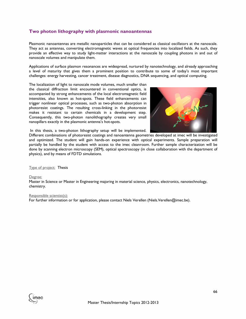
66
Master Thesis/Internship Topics 2012-2013
Two photon lithography with plasmonic nanoantennas
Plasmonic nanoantennas are metallic nanoparticles that can be considered as classical oscillators at the nanoscale. They act as antennas, converting electromagnetic waves at optical frequencies into localized fields. As such, they provide an effective way to study light-matter interactions at the nanoscale by coupling photons in and out of nanoscale volumes and manipulate them.
Applications of surface plasmon resonances are widespread, nurtured by nanotechnology, and already approaching a level of maturity that gives them a prominent position to contribute to some of today’s most important challenges: energy harvesting, cancer treatment, disease diagnostics, DNA sequencing, and optical computing.
The localization of light to nanoscale mode volumes, much smaller than the classical diffraction limit encountered in conventional optics, is accompanied by strong enhancements of the local electromagnetic field intensities, also known as hot-spots. These field enhancements can trigger nonlinear optical processes, such as two-photon absorption in photoresist coatings. The resulting cross-linking in the photoresist makes it resistant to certain chemicals in a development step. Consequently, this two-photon nanolithography creates very small nanopillars exactly in the plasmonic antenna’s hot-spots.
In this thesis, a two-photon lithography setup will be implemented. Different combinations of photoresist coatings and nanoantenna geometries developed at imec will be investigated and optimized. The student will gain hands-on experience with optical experiments. Sample preparation will partially be handled by the student with access to the imec cleanroom. Further sample characterization will be done by scanning electron microscopy (SEM), optical spectroscopy (in close collaboration with the department of physics), and by means of FDTD simulations.
Type of project: Thesis Degree: Master in Science or Master in Engineering majoring in material science, physics, electronics, nanotechnology, chemistry. Responsible scientist(s): For further information or for application, please contact Niels Verellen ([email protected]).

67
Master Thesis/Internship Topics 2012-2013
Plasmonic 2D crystals with gain
Surface plasmon polaritons(SPP) are electromagnetic excitations propagating at the interface between a dielectric and a metal. A strong coupling between electromagnetic fields and the oscillations in the metals electron plasma give rise to these waves. SPP’s are highly confined to the metal surface and have shorter wavelengths then the photonic equivalent. They are therefore interesting for sensing and miniaturization of optical circuits.
The use of SPP’s for optical circuits has however been quite challenging due to the high losses in the metal. Because of this, there has been much interest in adding gain to plasmonic devices. Optical gain introduced by fluorescent-doped dielectrics or semiconductors can compensate for metal losses extending the propagation length of the SPP’s. If the gain exceeds the metal losses this can even lead to lasing.
At imec a process has been developed that creates thin GaAs/AlGaAs wells on a silver surface. For this master thesis we propose patterning these layers to form 2D plasmonic crystals equivalent to photonic crystals, which can be used as a waveguide or as a resonator. By pumping the GaAs-layer we intend to introduce gain, improving performance of these plasmonic devices.
The student will use 2D and 3D finite difference time-domain simulation to better understand and design plasmonic crystals. He will learn to work in the imec cleanroom to processes the designed samples. The processed samples can be tested in the optical labs at Imec or the physics department.
Type of project: Thesis for 1 year. Degree: Master in Science or Master in Engineering majoring in physics. Responsible scientist(s): For further information or for application, please contact Dries Vercruysse ([email protected]).

68
Master Thesis/Internship Topics 2012-2013
Combining neuronal signal processing algorithms into Matlab-based graphical user interface platform for analysis of in vivo brain signals
In order to advance the understanding of the brain, its functions and interconnections, we need high resolution information, originating from many neuronal cells. Implantable microelectrode probes for neural recording and stimulation offer new insight and simultaneous observation of individual and group activity of neurons in certain volume of the brain. This makes them an important tool for investigation of neurophysiological systems as well as assisting neuroprosthetics developments (e.g. artificial limb control).
In the Bio-electronic Systems group of imec, state-of-the-art neural implants with microelectrode arrays are being developed. New features, like innovative electrode materials, probe designs and on-chip electronics are being implemented. These probes have to be evaluated in vivo before neuroscientists can use them in neurophysiological experiments. During the initial proof-of-concept in vivo evaluation of these new probes large amounts of neuronal data are generated, which has to be processed. This processing of the recorded signals aims at extracting features of interest that are related to neurophysiological properties, showing the changes and main signal features to the investigator who can relate them to the experiment conditions and extract valuable conclusions.
In this project, a candidate will first work in collaboration with biologists and get familiar with a process of acquiring signals from live animals using imec made neural probes. Then, a scalable, Matlab based platform is to be developed. It should demonstrate signal processing algorithms to obtain and show main features of real signals to the investigator. Starting from literature, existing commercial options and previously in-house developed software, the goal is set to develop software scripts which integrate desired options agreed upon into semi-automatic program. It should contain GUI for visualizing signals and its main features to the biologists. The platform aims at being easy-to-use, intuitive and upgradable, showing, among others, basic signal properties (like signal-to-noise ratio, basic noise level, LFP power etc.). The candidate will have the chance to participate in a dynamic team of multidisciplinary researchers in the field of bio-electronics.
Required background: extensive Matlab experience, signal processing
Type of project: Internship for 3 months. Degree: Master in Industrial Sciences or Master in Sciences or Master in Engineering majoring in biology, bio-electronics, biomedical sciences. Responsible scientist(s): For further information or for application, please contact Marleen Welkenhuysen ([email protected]).

69
Master Thesis/Internship Topics 2012-2013
Organotypic slice culture
Organotypic slice culture is an attractive in vitro method since it has semi-intact morphological and physiological properties of the neural network. This culture can be prepared from different parts of the brain, among them the hippocampal slice culture is a very interesting model to study long-term potentiation (LTP) mechanisms underlying mammalian learning and memory processes.
There are two major conventional methods to make the hippocampal slice culture; roller-tube and membrane culture method. In these techniques, hippocampi of young rodents (postnatal days 1-7) are dissected and horizontally cut into 350 µm in thickness. The slices are next placed on glass coverslips in a flat-sided tube or semiporous membranes. They continuously support the slices for exposing to the liquid-oxygen interface, which enables the slices to be maintained for several weeks with the original cytoarchitecture. However these methods can not be applied to the multi-electrode arrays (MEAs) therefore it is necessary to develop a new tool or modify the existing method. Our group is optimizing the hippocampal slice culture on the CMOS-based MEA surface featured with thousands of micronails. With this tool, we aim at stimulating and recording neuronal signals at nearly single cell level within semi-preserved neuronal networks and eventually investigating long-term monitoring of neuronal activity. We have recently developed a tilting device to culture hippocampal slices immobilized on a CMOS-MEA surface. Students who participate in this work will first learn preparing acute brain slices from rodents. When the preparation is successful, this platform will be validated for morphological recording and electrophysiological studies, such as recording Ca2+ and electrical activities and immunocytochemical staining.
Required background: Students should have experience with animal handling or at least they are willing to work with rodents in a daily basis. Experience with cell culturing is a plus.
Type of project: Thesis or internship for minimum 6 months. Degree: Master in Industrial Sciences or Master in Sciences or Master in Engineering majoring in biology, bioengineering. Responsible scientist(s): For further information or for application, please contact Dries Braeken ([email protected]).

70
Master Thesis/Internship Topics 2012-2013
V. Energy
Degradation mechanisms in organic solar cells
Organic photovoltaic devices are one of the most promising applications of organic semiconductors. As organic semiconductors can be manufactured by low temperature processes, such as printing from solution based inks, these materials are compatible with flexible plastic substrates resulting in a lightweight, inexpensive and very practical product. Over the last years impressive progress has been achieved in organic photovoltaic device efficiency and promising roll-to-roll compatible deposition techniques have been also reported. This rapid technological development brings applications close-by, and consequently also the importance of device reliability. Cost evaluations suggest that a lifetime of 5-10 years is necessary with current power conversion efficiencies to achieve low prices. Nevertheless, currently only 1 year of outdoor lifetime was reported on polymer solar cells, other studies in accelerated conditions estimated the device lifetime to 2-3 years. Currently, polymer solar cells are comprised of a multilayer stack of a transparent anode, a polymeric interlayer, a photoactive bulk heterojunction composed of polymer and fullerene capped with an evaporated cathode. Reaction with oxygen and humidity as well as light induces degradation both in the volume and at the interfaces of these layers leading to multiple concurrent degradation mechanisms. Therefore discriminating between the parallel mechanisms is one of the biggest challenges in reliability research. The focus of this master thesis lies in the investigation of the degradation of the organic/electrode interfaces. Implementation of new device architectures, advanced electrical measurements will assist the distinction between the simultaneously occurring degradation mechanisms. Most of the work will be done in the state-of-the-art organic device processing lab of imec. The student will receive a broad training on full device processing (spin-coating, metal evaporation) and characterization tools. After a short training period it is expected that the student can work independently and focusing on his/her investigation. Type of project: Thesis and internship of minimum 6 months.
Degree: Master in Industrial Sciences or Master in Engineering majoring in nanotechnology, physics, material sciences, electrical engineering. Responsible scientist(s): For further information or for application, please contact Eszter Voroshazi ([email protected]).

71
Master Thesis/Internship Topics 2012-2013
Solving the Caldeira-Leggett model with balance equations
Considering the electron-phonon interaction Hamiltonian bilinear in the electron and phonon coordinates, the Caldeira-Leggett (CL) model provides an exactly solvable time-dependent model for studying transport of electrons in a dissipative environment. On the other hand, a set of quantum mechanical energy and momentum balance equations has been developed some time ago to study the non-equilibrium features of an electron gas in the presence of various scattering mechanisms. In general, the resulting kinetic equations heavily rely on a clever choice of the constraints fixing a truncated set of non-equilibrium averages (energy, momentum, current, ...) as well as on the calculation of the corresponding Lagrange multipliers which determine the form of the (approximate) density matrix. In this work the balance equations will be solved for the Caldeira-Leggett model and the solutions will be compared with those obtained directly from the Heisenberg equations for the electron and phonon coordinates. In particular, the validity of the balance equation approach and its inherent density matrix will be critically assessed. Finally, the perspective of incorporating the difference between the CL model and the real electron-phonon interaction as a perturbation into the frictional force will be studied.
Type of project: Thesis of 8 months.
Degree: Master in Science majoring in physics. Responsible scientist(s): For further information or for application, please contact Wim Magnus ([email protected]) and Bart Soree ([email protected]).
Modeling ionic diffusion in solid-state materials for energy storage applications
The development of fundamental understanding in material science starts at the atomic level, where concerted movements set the properties of a material and its reaction upon the application of external factors. With the current development of nano-structured materials as e.g. metal-organic frameworks which can be used for energy storage applications, gaining insights into the dynamics that drive the evolution of a system along representative time window is becoming a problem of prime importance. With that respect, Molecular Dynamics (MD) has long proved to be a very robust and useful technique that offers unique insights into the dynamical behavior of a system. However, a large gap is often observed between the events captured by the MD simulations and the experimental observations, mainly due to the fact that monitoring the evolution of a non-equilibrium system towards its equilibrium state is computationally very demanding. We therefore developed a new technique which, together with other modern algorithms, is implemented in an imec software package. This software package will be the necessary tool to bridge the gap mentioned. The content of the project is then to further explore, develop and test these techniques with a striving to engineer novel materials for energy storage applications. The student will gain insight into modern first principle calculation executed on up-to-date infrastructure. Further he will get familiar with hot-topics in energy storage as solid-state batteries and experience how imec can make a difference in this field. In the beginning of the project a work schedule is made (together with the student!) with clear milestones which lead the student towards making significant contributions to the energy storage group insight imec.
Type of project: Thesis
Degree: Master in Science majoring in physics, chemistry. Responsible scientist(s): For further information or for application, please contact Geoffrey Pourtois ([email protected]).

72
Master Thesis/Internship Topics 2012-2013
Bonding of cells to glass for next-generation c-Si PV modules
Photovoltaics have always been mainly (over 80%) based on c-Si solar cells, and this will continue to be the case for the foreseeable future. The module technology used for connecting and protecting these cells likewise has been established already quite some time ago and has proven its worth with operational lifetimes exceeding 20 years in harsh outdoor conditions. However, cost (and other) considerations are continuously pushing technology development towards higher performance, longer lifetimes and cheaper materials and processing. But while this pressure has in the past mostly been focused on cell development, also module technology is now being pushed towards such improvements. With this in mind, imec is developing a module concept, coined i-module, that provides an alternative for the currently standard technology for making modules. The standard technology is based on stringing of cells for electrical interconnection and subsequent EVA lamination for encapsulation of these strings between a (transparent) front- and backsheet, whereas the i-module targets first bonding of the cells using a silicone adhesive, and only after attaching them to the glass, interconnect them. This way, the fragile cells are supported as much as possible during module manufacturing. As might be clear from the description, silicone bonding is a crucial part in this concept, and many aspects have to be taken into account: the silicone coating method and its parameters, the curing scheme and the bonding setup itself. In this topic, the idea is to optimize these processes, depending on the types of glass and wafers to be bonded: these can vary in thickness, in surface topography (texture) and surface finish.
Type of project: Thesis or internship of 6-9 months.
Degree: Master in Industrial Sciences or Master in Engineering majoring in material sciences (polymers), physics, electronics, ... Responsible scientist(s): For further information or for application, please contact Jonathan Govaerts ([email protected]).
Metal contacts for amorphous Si solar cell applications
Amorphous (a-)Si layers offer several advantages for the production of cost-effective, high efficiency Si solar cells. Apart from some beneficial intrinsic material properties, a-Si can be deposited at low temperature which facilitates cell processing and integration. At imec, the i-module concept is developed in which part of the back-contact cell processing is performed when the Si substrates are already attached to the module glass. This brings some restrictions for the thermal budget of the process steps and a-Si is therefore a well suited candidate for fabricating the active layers. One of the critical parts for integrating a-Si in successful (solar cell) devices is maintaining the a-Si layer quality after metal deposition and establishing a low contact resistance. Due to the lower amount of active dopants it is a challenge to form a low Ohmic contact. A proper combination of tuning the a-Si properties and choosing the right metal and deposition conditions is required for optimizing the metal contact. While the main focus for this position will be on the metallization part, this work will be in close collaboration w/ different members of the ‘Thin c-Si Solar Cell and Modules’ team working on a-Si layer optimization. This includes sample preparation by using different processing techniques like photo-lithography, and PVD (Physical Vapour Deposition), as well as electrical characterization of various test structures and material combinations.
Type of project: Internship of minimum 4 months.
Degree: Master in Industrial Sciences or Master in Engineering majoring in material sciences, physics or electronics. Responsible scientist(s): For further information or for application, please contact Riet Labie ([email protected]).

73
Master Thesis/Internship Topics 2012-2013
Radio-frequency communication with metal-oxide electronics on plastic
In recent years, fast progress was made in the technology of thin-film semiconductor devices based on organic semiconductors (such as pentacene and derivatives) and oxides, such as Indium-Gallium-Zinc-Oxide (GIZO). In particular this latter semiconductor offers over amorphous silicon the advantages of a much higher carrier mobility, of the order of 10 cm2/Vs, and room temperature processing, making it fully compatible with plastic substrates. This new technology opens the way to circuits and systems fabricated directly on flexible plastic foil. RFID transponders and tags are one type of application that will greatly benefit from this opportunity. The crucial component of a passive RFID tag is the rectifier, which must operate at HF (13.56MHz) or more preferable at UHF (869MHz). The diodes must follow the high-frequency input signal, still providing enough power supply for the tag circuitry, which is accomplished only by optimized devices with low leakage current and charge transient time. These devices can have mainly two topologies: the Schottky and transistor connected diodes. Transistor-diodes are based on a shorted gate-drain transistor configuration. In this configuration, the gate-drain electrode and the source act as the injector and the blocking electrode, respectively. The main advantage of such topology is the integration with other circuitry, as exactly the same process technology as for standard transistors can be used for its fabrication. Their main drawback, on the other hand, is the relatively long minimal channel length that can be achieved with standard photolithographic processes.
The main task of the student is to investigate the effects of GIZO deposition on the transistor-diode characteristics, in order to achieve high on/off drain currents and high electron mobility, targeting mainly the transistor onset voltage control. This activity includes the fabrication of devices within imec clean room and our laboratories using mainly two deposition techniques: RF sputtering and thermal evaporation. The second step will be to integrate these single devices in a rectifier with integrated capacitances and characterize its frequency response. Initially, the devices will be fabricated on a hard substrate such as silicon, but the final device should be completely realized on a flexible plastic carrier. In order to develop insightful ideas about the diode performance, all experimental work will be followed by analytical and SPICE model.
Type of project: Thesis or internship of 6 months.
Degree: Master in Science or Master in Engineering majoring in material physics, electronics, nanotechnology. Responsible scientist(s): For further information or for application, please contact Adrian Chasin ([email protected]).

74
Master Thesis/Internship Topics 2012-2013
Morphological control of organic bulk solar cells
Organic photovoltaics (OPV) are an emerging technology in the PV field. The core of OPV cells are carbon based materials, in contrast to the traditional, silicon based technologies. The material choice is endless, and encompasses both polymers as well as small molecules. The more critical material characteristics are decent semiconducting properties and an absorption spectrum that covers part of the solar spectrum.
In this research, the focus will be on small molecule OPV devices, made by thermal evaporation. In its most basic form, you need both an electron (=acceptor) and a hole conducting (=donor) material to generate a photocurrent. More efficient architectures use a mixture of donor and acceptor material in the same layer. For thermal evaporation, this can be achieved by co-evaporating the two layers, creating a dense blend. Next to the composition of this blend, its structure is equally important. he used materials have a crystalline nature, determining their absorption spectrum, while an increased crystallinity of the active layer induces higher charge carrier mobilities, which is beneficial for the conversion efficiency. By selecting the correct evaporation conditions, a limited control on the morphology and crystallinity of the blend can be achieved. More control is possible by using a templating layer underneath the blend, and by post-deposition treatments such as thermal or solvent annealing.
Your task will be the investigation of these processing steps, and selecting the optimal ones to create a donor-acceptor mixture that leads to efficient solar cells. You will be involved in the processing of the cells, as well as the characterization afterwards. The focus will be on lab work, but post-processing the data, and correlating the processing steps with the characteristic parameters (absorption, electrical, morphology) is very important.
Type of project: Thesis or internship of 4-5 months.
Degree: Master in Science or Master in Engineering majoring in nanoelectronics, material sciences, physics.
Responsible scientist(s): For further information or for application, please contact David Cheyns ([email protected]) and Kjell Cnops ([email protected]).

75
Master Thesis/Internship Topics 2012-2013
Spectral characterization of organic tandem solar cells
Organic photovoltaics (OPV) use carbon based semiconductors for the photon-to-carrier conversion. These materials have the advantage of easy processing, with low thermal stress on the used substrate. However, the disadvantages are charge carrier mobilities that are a few orders of magnitude lower than in silicon, and narrow absorption spectra. These facts limit the overall conversion efficiencies of OPV cells, with a world record of 10% at the time of writing.
Tandem cells provide a solution to overcome the narrow absorption spectra. In this configuration, two stacked subcells are electrically connected in series. Each subcell utilizes different materials with complementary absorption spectra, and the combination of these materials guarantee a good overlap with the solar spectrum.
The topic of this internship will be the development of characterization techniques to probe the separate subcells of these tandem stacks. The main focus is the deconvolution of the spectral responses of both subcells. This involves opto-electrical measurements in combination with optical simulations. To this end, you will adapt an existing characterization system and simulation software. Once operational, you will give feedback for a device stack with optimized conversion efficiency.
Type of project: Thesis or internship of 4-5 months.
Degree: Master in Science or Master in Engineering majoring in nanoelectronics, physics.
Responsible scientist(s): For further information or for application, please contact David Cheyns ([email protected]).
Tunneling barriers for the passivation of metal contacts in silicon solar cells
Photovoltaic is a fast growing field, dominated by crystalline silicon solar cells. Yet there remains a significant difference between the theoretical efficiency one could reach and the efficiency actually reached with these cells, and this both in production lines and in laboratories. Part of the efficiency loss comes from the interface between silicon and the metallic contacts of the cell: at this interface, light-generated free carriers recombine without being collected by the cell contacts. To reduce the recombination rate, a thin dielectric layer, a so called tunneling barrier, can be included between silicon and the metallic contact. If well chosen, this dielectric leads to a reduction of the recombination rate. At the same time, the dielectric layer should be thin enough to allow for tunneling of the charge carriers through it. While it has already been shown that tunneling barriers can lead to a cell efficiency increase, your objective is here to investigate dielectric layers that could be used for contact passivation.
This work is experimental. The student will join a team of scientists from all around the world to work in laboratories and cleanroom for processing silicon structures, characterizing them and analyzing your results. He/she should have a liking for lab-work and a good knowledge of written and spoken English.
Type of project: Thesis and/or internship of minimum 6 months.
Degree: Master in Industrial Sciences or Master in Engineering or Master in Science majoring in physics, material sciences, nanotechnologies, ...
Responsible scientist(s): For further information or for application, please contact Xavier Loozen ([email protected]).

76
Master Thesis/Internship Topics 2012-2013
Development of amorphous silicon deposition for silicon heterojunction solar cells
By deposition of amorphous silicon on monocrystalline silicon, cost-effective, world-record efficiency solar cells can be fabricated. This is because amorphous silicon has some beneficial intrinsic material properties. Moreover, it is deposited at low temperatures (<200°C) which brings about unique possibilities, but also restrictions, for cell processing and integration. At imec, a new concept for cell integration (termed “i-module”) has been developed that requires particularly good control over amorphous silicon deposition. For this purpose, a state-of-the-art deposition tool (PECVD, Plasma-enhanced chemical vapor deposition) has been purchased and installed. Following initial start-up of the tool, deposition processes need to be developed. Typical requirements for these deposition processes are: low recombination velocities at the a-Si/c-Si interface, maximum dopant activation and low contact resistivity. Examples of characterization methods are: spectroscopic ellipsometry, quasi-steady-state photoconductance, infrared absorption. The focus of this internship is the deposition and characterization of amorphous silicon layers. The student will work and interact with a team of experts, and the results will be followed up closely. At the same time it is expected that the student takes initiative and is able to work independently once the initial training period has finished. It is expected that the students write high-quality reports at the conclusion of the internships (this can be a thesis).
Type of project: Internship of minimum 6 months, possibly with thesis.
Degree: Master in Science or Master in Engineering majoring in material sciences, physics, electronics, chemistry. Responsible scientist(s): For further information or for application, please contact Twan Bearda ([email protected]).

77
Master Thesis/Internship Topics 2012-2013
CIGSSe and CZTSSe films formation from selenization/sulfurization of metals and chalcogenide compounds
Chalcogenide thin film based solar cells display a record conversion efficiency above 20 %. Basically, two ways for the film deposition are followed. The first one, leading to the higher efficiencies, implies the co-evaporation process, preformed under vacuum (~10-6mbar) and at high temperature (~600ºC). In the aim of reducing the photovoltaic modules production cost, the deposition at low temperature of the metal precursors and, if possible, according a non-vacuum process, then followed by a chalcogenization (Selenium, Sulfur) step, constitutes the second exploratory way.
At IMEC, the research efforts are focused on this second approach and more particularly on the Cu(In,Ga)(S,Se)2 and Cu(Zn,Sn)(S,Se)2 based solar cells. The material precursor from the first family (ink-based) is deposited by non-vacuum wet-coating process, while the second one arises from sputtered metals. The proposed master thesis will take an interest in the thermal selenization/sulfurization process, necessary for the final active layer formation. By adjusting different parameters (H2S/H2Se gas flows, substrate temperature ...), the goal is to understand the physico-chemical phenomenon understandings occurring during this chalcogenization process in the aim of obtaining an efficient conversion from the initial precursor layer to the final active thin film layer in term of photovoltaic properties. At different steps, the electrical and optical properties of the layers will be characterized, mainly by scanning electron microscopy, X-ray diffraction, 4 points probe measurements, photoluminescence and Hall effect. The influences on the current-voltage characteristic and the spectral response of the complete solar cell will be followed as well. Dependent on the quality of the layers, also improvements in the solar cell processing, like the formation of an alternative hetero-junction can be studied.
Type of project: Preferably thesis, but 3 months internship is also possible.
Degree: Master in Science majoring in material sciences, semi-conductor physics and electronics. Responsible scientist(s): For further information or for application, please contact Guy Brammertz ([email protected]).

78
Master Thesis/Internship Topics 2012-2013
Characterization and power-loss analysis of interdigitated back contact (IBC) silicon solar cells
Photovoltaic is a fast growing field, dominated by crystalline silicon solar cells. In several roadmaps it is predicted that back contact solar cells, with all metal contacts located at the rear of the solar cell, will become a more prominent cell structure in the next years. Interdigitated back contacts are introduced to increase the conversion efficiency of crystalline silicon solar cells and allow for further reduction of the cell thickness, simplification of module fabrication and improved aesthetics of the final solar cell modules. At imec we have developed a high efficiency baseline process for small area IBC silicon solar cells, reaching efficiency conversion values up to 23%. In the next year this baseline process will be further optimized and upscaled to larger wafer and solar cell area. Characterization and analysis of the realized IBC solar cells is crucial, such that the experimental work can be focused on those parts of the solar cell where the losses are dominating. This is done by means of a power-loss analysis, giving an overview of the magnitude of all the loss elements within the realized solar cells. As input of this power-loss analysis, a detailed characterization of the solar cells and test wafers is performed. In this thesis you will learn how to perform the characterization and analysis of realized solar cells, you will get to understand the power-loss analysis and use it to indicate where to improve the subsequent solar cell runs, both in terms of process optimization and solar cell design. As this work is focused on characterization and analysis of solar cells, you require a basic knowledge of device physics; preferably already you have knowledge on solar cell physics. You will join a team of scientists from all around the world to characterize the solar cells and analyze your results. You should have a liking for device characterization and device physics and a good knowledge of written and spoken English.
Type of project: Thesis and/or internship of minimum 6 months.
Degree: Master in Industrial Sciences or Master in Science or Master in Engineering majoring in physics, materials science, nanotechnologies.
Responsible scientist(s): For further information or for application, please contact Niels Posthuma ([email protected]).

79
Master Thesis/Internship Topics 2012-2013
Reliability testing of c-Si solar cells with Cu plated metallization
Replacing the standard Ag screen printed front side metallization in c-Si solar cells by electroplated Cu may lead to significant cost reductions as well cell performance improvements. Apart from the obvious lower raw metal cost, the benefits for introducing Cu also involve the potential for increasing the efficiency by reducing the front surface shading area, lowering the overall resistance and limiting the recombination losses. Despite these advantages, due to the required 20-to-25 years of customer warranty, the module manufacturers are still rather reluctant for introducing such new materials with an unknown track record of in-the-field performance. Therefore, further investigation of the reliability is still needed before industrialization can occur. In general, the qualification procedure for PV modules involves the application of standardized test protocols (IEC-standards). For new technologies like Cu-metallised cells, other degradation mechanisms may become more dominant and current qualification tests may no longer be relevant. For instance, Cu is known to be more sensitive to thermal and humid environments compared to Ag and therefore adjustments of the currently used standard test conditions may be needed.
The objective of this work is to perform various accelerated ageing tests in order to get a better understanding of potential new failure mechanisms. This work will involve testing finished solar cells and monitor the different cell parameters as function of the environmental conditions. Furthermore, the aim is to investigate and prepare other (simplified) electrical test structures and measure the impact of the presence of Cu on these device characteristics.
Type of project: Thesis
Degree: Master in Industrial Sciences or Master in Science or Master in Engineering majoring in physics, material sciences, electronics.
Responsible scientist(s): For further information or for application, please contact Riet Labie ([email protected]).
Copper contact plating for advanced solar cell contacts
Solar cells are a vital part of the energy mix of the future. Imec develops advanced solar cells, aiming at pushing their efficiencies towards the theoretical limits. A new concept that is currently explored is a cell that makes use of an advanced junction of an amorphous nano-layer. In order to fully exploit the potential of such a cell, imec wants to make use of copper as a conductor material to extract the current. Copper has the advantage of being much cheaper than the more commonly used silver metal, without giving in too much on the conductivity side. That is what this thesis is about: What is the best way to put copper lines on a very advanced and thin layer? Can we improve it by alloying? Or by using different deposition parameters? Will it be reliable?... To answer these questions you will work together with experienced researchers from the imec photovoltaics team, defining the right questions, setting up a plan and making it happen.
Type of project: Thesis with internship of minimum 6 months.
Degree: Master in Industrial Sciences or Master in Science or Master in Engineering majoring in material sciences, electrochemistry, surface technology, thin films ( electronics, physics or chemistry).
Responsible scientist(s): For further information or for application, please contact Joachim John ([email protected]), Jan Vaes ([email protected]) and Jef Poortmans ([email protected]).

80
Master Thesis/Internship Topics 2012-2013
EBIC analysis of thin-film polycrystalline-silicon solar cells
Thin-film (TF) polycrystalline-silicon (pc-Si) solar cell technology combines the low-cost potential of a thin-film silicon technology with the high-efficiency and stability of the crystalline Si photo-voltaic technology. One of the key challenges in pc-Si technology is to control the grain growth to minimize the effect of the grain boundary and the intragrain defects. The electron beam induced current (EBIC) measurement technique is well suited for defect analysis of pc-Si structures as it allows the direct visualization of defects on sub-micrometer scale. In EBIC measurements, the electron beam of a scanning electron microscopy (SEM) system is used to locally generate free carriers in the absorber layer of the solar cell operating in short circuit conditions. By correlating the electron beam position with the collected current, information about the local recombination can be obtained. Typically the amount of the induced current is qualitatively (not quantitatively) visualized as brightness in the SEM image. The induced current is typically three orders of magnitude higher than the incident SEM beam current allowing for relatively sensitive measurements with high lateral resolution. At imec the EBIC measurement mode is available as an add-on of the nanoprober (NP) tool. The nanoprober combines a SEM tool, an electrical parameter analyzer and several nanomanipulators in one unit. The use of the NP for EBIC allows local contacting of structures with high precision. This enables to study very small structures at any place on the sample surface. All the components of the NP can be remotely controlled with a computer which allows automatization of repeated measurements. The focus of this internship will be the combination of direct electrical measurements with EBIC imaging to obtain quantitative information of the observed defect properties. An important part of the work is to implement a software control of the SEM beam position and parameter analyzer in order to make quantitative line and 2D current measurement possible. Next the newly developed quantitative EBIC measurements will be combined with the high precision needles of the NP tool. By measuring the collected current in function of the position of one of the nanoprobes, information about the carrier diffusion length in the material and carrier transport across grain boundaries can be obtained. The achieved capabilities will then be used to investigate different polycrystalline silicon material under different measuring conditions (external junction bias voltages, SEM beam energies,..). This internship topic involves both the advanced use of existing tools and techniques (EBIC and SEM) as well as the further development of these techniques by computer control (LabVIEW) of the nanomanipulators, the parameter analyzer and the SEM. Thus, proficiency in experimental work and computer skills are required from the candidate. The student will be part of the materials and component analysis (MCA) department and will interact also closely with members of imec’s photovoltaic program.
Type of project: Internship of 6 months.
Degree: Master in Industrial Sciences or Master in Science or Master in Engineering majoring in material sciences, physics, electrical engineering, ...
Responsible scientist(s): For further information or for application, please contact Kai Arstila ([email protected]) and Thomas Hantschel ([email protected]).

81
Master Thesis/Internship Topics 2012-2013
Raman and EDS analysis for thin-film solar-cell applications
Thin-film (TF) photo-voltaic (PV) cells are the focus of extensive research as alternative to common poly- and mono-crystalline Si cells. Despite their lower conversion efficiencies, they are looking promising mainly as they can be fabricated from less material (Si needs about 40 microns for being able to absorb >90% light). Thin-film PV cells aim to use direct band-gap materials with a thickness of 1-2 µm to absorb >90% light. Besides the established TF cells based on amorphous Si (a-Si), cadmium telluride (CdTe), and copper indium gallium selenide (CIGS), alternative material systems are being studied. One promising material route which is being explored at the moment are metal-sulfur / metal-selenium combinations such as Cu-Zn-Sn S/Se (CZTS). They allow for bandgap and band alignment engineering between 1-2 eV which is perfect for multi-junction cells by adjusting the S/Se ratio. Moreover, they are made from abundant and safe materials (Cu, Zn, Sn, S, Se, ...). Recently, a cell of Cu2ZnSnSe4 was demonstrated with 10% efficiency. The main obstacles to obtain high-performance cells based on CZTS are the control of stoichiometry and crystal phases. Therefore, dedicated characterization knowhow is essential.
Energy dispersive X-ray spectroscopy (EDS) looks suited to probe the stoichiometry of the micrometer thin films with sufficient spatial resolution. In EDS, the electron beam of a scanning electron microscopy (SEM) system is generating element-specific X-rays when hitting the sample. This can be used to quantify the thin-film composition. Raman is an optical technique and relies on inelastic scattering of photons which means that the energy of photons in monochromatic light changes upon interaction in a sample. It was recently suggested and demonstrated that Raman can be used for characterizing the crystal phases within a CZTS-based system. Both EDS and Raman are non-destructive and allow also for two-dimensional (2D) mapping.
The goal of this internship is to use Raman for studying the crystals phases and EDS for studying the composition of CZTS-based thin films for solar applications. Thin-films of known composition will be used for calibration. The analysis results will be used as feedback for improving the synthesis of CZTS stacks. For Raman a comparison will be made with X-ray diffraction (XRD) which is commonly used for studying crystal phases but which seems to suffer from peak overlaps. The student will work in a state-of-the-art materials characterization lab and will be trained in Raman, SEM and EDS. He/she will be part of the materials and component analysis (MCA) department and interact also closely with members of imec’s PV program.
Type of project: Internship of 6 months.
Degree: Master in Industrial Sciences or Master in Science or Master in Engineering majoring in material sciences, physics, electrical engineering, ...
Responsible scientist(s): For further information or for application, please contact Kai Arstila ([email protected]) and Thomas Hantschel ([email protected]).

82
Master Thesis/Internship Topics 2012-2013
Organic solar-cell material characterization by TOF-SIMS
A significant fraction of the cost of solar panels comes from the photoactive materials and sophisticated, energy intensive processing technologies. Recently, it has been shown that inorganic components can be replaced by semiconducting polymers capable of achieving reasonably high power conversion efficiencies. These polymers are inexpensive to synthesize and can be solution processed in roll-to-roll fashion with high-throughput. There is however still a large number of challenges to be overcome to improve the technology that imply sophisticated material analysis techniques. TOF-SIMS has long been applied to organic material but has often been limited by its difficult interpretation and by the loss of information during sputter profiling. Recent technological development (Cluster ion source, …) and theoretical ones (combination of several spectra from the same surface with different analysis source, known as G-SIMS) have open the possibilities for the characterization of polymer material. The objective of this work is to investigate the possibilities of TOF-SIMS analysis through this new development for materials related to organic solar cells such as P3HT, PCBM, PEDOT, PSS, CuPc, C60. This project will be mostly devoted to the profiling of these materials in multi layers or in blend. It has been shown that the optimal sputter condition in order to preserve organic information may differ from material to material, but little is understood of the origin of these differences. This will thus not only be devoted to finding optimal conditions, but also to understand (predict) which conditions should be used for an arbitrary material. The most recent innovation in TOFSIMS profiling of organic materials is the introduction of large gas-clusters as sputter source. This thesis will be performed on one of the first commercial source installed in the world on a TOFSIMS instrument. At the end of this thesis, it is expected on one side that conclusion will be drawn on the usability of TOFSIMS as a valuable analysis technique and on the other side to improve the understanding of physico-chemical effects happening during sputtering in order to narrow down the profiling options of polymers.
Type of project: Thesis of 6 months.
Degree: Master in Science or Master in Engineering majoring in physics, chemistry, material sciences.
Responsible scientist(s): For further information or for application, please contact Thierry Conard ([email protected]).

83
Master Thesis/Internship Topics 2012-2013
Characterization of organic materials using UHV conductive AFM at low temperatures
C-AFM (Conductive Atomic Force Microscopy) is an AFM based technique wherein a small conductive tip (moved via a piezo-electric control) is used to measure simultaneously topography and current map of a material at the nanometer scale. C-AFM represents an attractive approach to probe at controlled very low forces (nano/pico newton range) organic material systems, enabling to correlate structural variations with the electrical properties. The pioneering work of Park et.al [Nature 407:57 (2000)] has demonstrated that low temperature measurements are important in understanding conducting mechanism of the molecule. Many molecular systems have shown to behave as quantum dots, showing single electron charging behavior. The objective of the project is to investigate the current conduction seen through vertically aligned self assembled monolayers and conductive polymers at low temperature (liquid N2) in UHV environment and variation of conductance with respect to variation in chain length of the molecule, using conductive AFM technique. Self Assembled Monolayers dealt in this project have conducting properties with aromatic rings with chain length varying from 0.2nm to 0.7nm. Objectives to achieve and understand: • Charge injection and Charge transport through the molecules • Effect of Loading Force/Contact force on conductance • Effect of Tip work-function on conduction Type of project: Thesis or internship of 6 months.
Degree: Master in Industrial Sciences majoring in electrical/electronic engineering.
Responsible scientist(s): For further information or for application, please contact Ravi Chintala ([email protected]) and Pierre Eyben ([email protected]).

84
Master Thesis/Internship Topics 2012-2013
Characterization and modeling of Back-surface field formation in Si-based solar cells
In order to obtain high performance solar-cells, it is important to minimize the minority carriers recombination at the rear contact. In advanced solar cell concepts, like the i-PERC solar cell developed at imec, this is done by creating a locally defined, highly doped layer of the same carrier type as the base substrate. This layer, named back surface field (BSF), induces an electric field which shields minority carriers from recombining. As the doping level and extent of this BSF impacts strongly on the solar cell efficiency it is important to optimize its formation process.
A common approach used to create this BSF is by forming a local backside contacts using local laser ablation to open a hole in the passivation layer, coat the surface with an aluminum layer and to perform a heat treatment which leads to Al-incorporation in the Si-lattice.
The fundamental mechanisms leading to this incorporation and BSF formation can be understood from the details of the Al-Si phase diagram. Using cross-sectional scanning spreading resistance microscopy (SSRM), we have already studied the two-dimensional dopant (Al) maps of the BSF and analyzed the thickness, shape and maximum carrier concentration for various processing conditions (Al layer thickness, thermal budget, size,..) The SSRM results demonstrate a highly p-doped layer (~ 2 e19at/cm3) in a quasi-conformal shape around the solidified Al in the Si-etch pit creating the BSF-field.
The objective of the project is to explore the impact of the experimental processing conditions (Al-layer thickness and temperature budget, size of the opening,..), on the detailed shape of the etched region, the Al-incorporation and extent of the BSF. This work will be a combination of experimental observations with SSRM, (SEM,..) and finite element (heat) modelling in order to develop a comprehensive module for the BSF formation.
Type of project: Thesis of 6 months.
Degree: Master in Industrial Sciences or Master in Science majoring in electrical/electronic engineering.
Responsible scientist(s): For further information or for application, please contact Pierre Eyben ([email protected]) and Angel Uruena De Castro, ([email protected]).

85
Master Thesis/Internship Topics 2012-2013
Initiation of random pyramid formation: impact of contamination and surface roughness
One of the factors contributing to solar cell efficiency is its ability to as much as possible absorb the incident light. Two techniques are combined to reduce the amount of light reflected on the solar cell: texturing the surface of the solar cell and the deposition of an anti-reflective coating. The most efficient (industrial) texturing process consists of a random distribution of pyramids. These pyramids are formed due to the anisotropic etching properties of alkaline mixtures. These pyramids need a nucleation/initiation site before the pyramid is recessed into the silicon. The nature of this nucleation site is still uncertain. In order to get more insight into the nature of these nucleation site, the impact of contamination (metal, particles or organic) on random pyramid formation will be investigated during the alkaline etching. In addition the impact of the surface roughness will be investigated.
The experiments will consist of: • Adding and quantifying controlled changes to the Si surface prior to alkaline texturization • Controlled changes to the alkaline texturization mixture • Measuring the random pyramids (reflectivity, pyramid size (distribution), pyramid density)
Type of project: Thesis and/or internship.
Degree: Master in Industrial Sciences or Master in Science majoring in material sciences, chemistry.
Responsible scientist(s): For further information or for application, please contact Herbert Struyf ([email protected]) and Paul Mertens ([email protected]).

86
Master Thesis/Internship Topics 2012-2013
Photonic nanostructures for light management in novel thin silicon solar cells and modules
Context Silicon based solar photovoltaic cells represent more than 90% of the photovoltaic panels presently sold in the world; silicon is one of the most abundant materials on earth. In such cells, more than 1/3 of the cost is due to the silicon itself. Indeed, its purification and crystallisation have an important energetic and economical cost. This is why the photovoltaic research community is presently looking for ways to have solar cell structures based on thinner and thinner silicon layers. There are nevertheless limitations, existing for thick cells and becoming crucial for thin cells: the thinner the material, the lower its light absorption, in particular at long wavelengths (near infrared), due to the low absorption of Silicon. Thus, in order to keep the light absorption high, it is necessary to find light scattering and trapping techniques inside the absorbing silicon layer. Imec frame Imec is developing novel approaches to decrease the cost of silicon solar cells, including going to thinner silicon layers (40 to one micron). For such thin cells, the regular light scattering approach used for today’s thick cells (> 150 µm) by texturisation of the silicon surface) will not be sufficiently effective anymore. We propose therefore to develop light scattering and light trapping techniques to compensate for these losses. This means concretely: Understanding the optical losses of such structures thanks to home-made optical simulations. (Simulation tool: CAMFR based on Python, possibly Lumerical) as well as various optical characterisation techniques. Exploring schemes to enhance the light trapping in order to enhance absorption, while keeping good electrical properties.
For this 2nd point the imec Photovoltaics group is exploring several approaches: • Nanopatterned diffractive structures: we are developing nanopatterning techniques based on novel lithography
techniques: nanoimprint lithography, hole-mask colloidal lithography (pseudo-random) and plasma or solution-based etching techniques, allowing to strongly modify the optical properties of a solar cell stack.
• Dielectric Bragg reflector that increase the reflection to almost 100 % in the near-IR . • Metallic or dielectric nanoparticles to scatter light into the layers.
Internship description In this frame, it is proposed to interns (between 3rd and 5th year of Master or equivalent) to participate to the numerical modelling of solar cells with and without light-management features, as well as to some aspects of the experimental part, in particular nanoimprint lithography and solar cell characterisation. Type of work: experimental and simulations
Type of project: Thesis or internship
Degree: Master in Science or Master in Engineering majoring in physics, electrical engineering, material science, chemistry
Responsible scientist(s): For further information or for application please contact Ounsi El Daif ([email protected]).
87
Master Thesis/Internship Topics 2012-2013
Investigation on laser enhanced metal-silicide formation for novel front contact schemes on silicon solar cells
Silicon solar cells are the working horse in photovoltaics (PV) industry by a market share of more than 85% of the modules produces for roof top installations. The request for cheaper modules and finally reach grid parity is translated to a need for thinner solar cells with an increase in conversion efficiency. In order to reach this goal novel cell concepts have to be developed for implementation in industrial process lines. Imec’s PV department is working on these novel cell concepts to accelerate the development toward lower cost/watt peak for solar energy production. While in today’s production the contact formation is mainly performed by thick film techniques like printing metal containing paste through patterned screens, thinner cells (well below 150um) requires more and more non-contact metallization techniques like light induced plating. A second requirement is the mitigation from rather expensive silver containing contacts towards silver-free metallization concepts like copper based contacts. In the imec PV department different metal contact schemes are investigated, like Ni/Cu/Ag stacks, etc. The nickel layer typically is deposited 1um thick acts as a barrier layer. In order to provide a reliable adhesion of the front contact, a NiSi layer is formed under thermal annealing. The silicidation process can be performed in a furnace heating up the whole device or preferred locally with a laser annealing process. For solar cell processing laser annealing is interesting due to the potential to improve control over the silicidation process and limit diffusion of nickel towards the junction. Enabling new cell architectures and enhanced cell efficiencies. Further advantages are seen due to the localised heating effect enabling for example temperature sensitive rear passivation schemes to be employed. The student will participate in the team that investigates Copper based front contact schemes on their physical and electrical properties and implement the contact layer stack into silicon solar cells. Characterizing methods like TLM and pseudo fill factor measurements are used to determine the contact performance. The student will be trained on advanced silicon Solar Cell contact development, characterization and the interpretation of the achieved results.
Type of work: Experimental Type of project: Thesis
Degree: Master in Science or Master in Engineering majoring in physics, electrical engineering, material science, chemistry
Responsible scientist(s): For further information or for application please contact Loic Tous ([email protected]) and Richard Russell ([email protected]).

88
Master Thesis/Internship Topics 2012-2013
Investigation on laser enabled boron doping activation for novel silicon solar cell concepts
Silicon solar cells are the working horse in photovoltaics (PV) industry by a market share of more than 85% of the modules produces for roof top installations. The request for cheaper modules and finally reach grid parity is translated to a need for thinner solar cells with an increase in conversion efficiency. In order to reach this goal novel cell concepts have to be developed for implementation in industrial process lines. IMEC’s PV department is working on these novel cell concepts to accelerate the development toward lower cost/watt peak for solar energy production. After the implantation of dopants into silicon, the implanted species, like boron, have to be activated in order to get electrically active, providing a higher carrier concentration. This effect is used on p-type silicon base material to perform highly doped regions on the rear side of the solar cell. These back-side fields (BSF) are passivating the surface by repelling negative charges from the interface. Conventionally the post-implantation activation is performed by a thermal treatment using a furnace. In the case of boron this can go above 1000C. This high thermal budget could be avoided by laser annealing of the boron doped silicon layer. The post-implantation laser annealing has been already successfully introduced in CMOS devices and is studied now also on silicon solar cells. The substitution of the high temperature furnace annealing by laser annealing has the potential to reduce seriously the cost/watt peak in cell manufacturing. The student will participate in the team that investigates boron implanted BSF schemes on their physical and electrical properties and implement the highly B-doped layer into silicon solar cells. Characterizing methods like SIMS and minority carrier lifetime measurements are used to determine the layer performance. The student will be trained on advanced silicon Solar Cell BSF development, characterization and the interpretation of the achieved results. Type of work: Experimental Type of project: Thesis
Degree: Master in Science or Master in Engineering majoring in physics, electrical engineering, material science, chemistry
Responsible scientist(s): For further information or for application please contact Angel Uruena ([email protected]).

89
Master Thesis/Internship Topics 2012-2013
Circuit modeling of interconnection schemes for thin film PV modules
Next to Si-based solar cells, devices based on chalcogenide thin films, such as CdTe and Cu(In,Ga)(Se,S)2 (CIGS), are at the forefront in thin film solar cell technology. CdTe solar cells are now the largest thin-film technology in production with typical commercial module and record cell efficiencies of 10% and 16.7%, respectively. In the meantime, CIGS technology, as the main thin-film competitor, has reached module and cell efficiencies of 9%–12% and 20.1%, respectively. Thin Film-PV (TF-PV) modules have to compete with present efficiencies of silicon solar cells above 20%.
Although lab efficiencies for CIGS cells are above 20%, module efficiencies are typically below 13%. Part of this drop in efficiency can be attributed to the problem of scalability of the absorber material to large areas. But careful first analysis has shown that a substantial part (>2-4% in absolute efficiency) of the efficiency reduction can be attributed to the interconnection scheme used in TF-PV.
The goal of this master thesis is first to build –up a circuit model for TF-PV modules, using a realistic solar cell equivalent circuit. The program SPICE will be used for building this circuit model. The model will be build for different interconnection concepts in order to calculate for each of them the efficiency reduction under realistic solar module working conditions. This will allow optimizing the interconnection scheme in TF-PV modules and finding a balance between more complex interconnection schemes (i.e. higher cost) and an increased efficiency (i.e. higher gain).
Besides optimized interconnection schemes, also the impact on module efficiencies of a local defect in the absorber layer will be simulated. This can be done by using existing equivalent circuit parameters for some of the known TF-PV defect modes and implementing these parameters in the SPICE model. Also in this case, different interconnection schemes will be simulated to calculate the robustness of the module efficiency versus the existence of certain defects in the TF-PV module.
Dependent on the simulation results, even the introduction of extra active or passive components in the thin film circuit can be evaluated in order to evaluate the robustness of the TF-PV module efficiency against defects.
Type of project: Thesis
Degree: Master in Engineering or Master in Science majoring in electronics, nanoelectronics, energy Responsible scientist(s): For further information or for application please contact Marc Meuris ([email protected]) and Francky Catthoor ([email protected]).

90
Master Thesis/Internship Topics 2012-2013
Alternative assembly technologies for next-generation c-Si PV modules
Photovoltaics have always been mainly (over 80%) based on c-Si solar cells, and this will continue to be the case for the foreseeable future. The module technology used for connecting and protecting these cells likewise has been established already quite some time ago and has proven its worth with operational lifetimes exceeding 20 years in harsh outdoor conditions. However, cost (and other) considerations are continuously pushing technology development towards higher performance, longer lifetimes and cheaper materials and processing. But while this pressure has in the past mostly been focused on cell development, also module technology is now being pushed towards such improvements. With this in mind, imec is developing a module concept, coined i-module, that provides an alternative for the currently standard technology for making modules. The standard technology is based on stringing of cells for electrical interconnection and subsequent EVA lamination for encapsulation of these strings between a (transparent) front- and backsheet, whereas the i-module targets first bonding of the cells using a silicone adhesive, and only after attaching them to the glass, interconnect them. This way, the fragile cells are supported as much as possible during module manufacturing. In addition, other components may be incorporated at the same level as the cells for additional functionality of the module. In this topic, the idea is to investigate the possibilities and limitations of the involved technologies, as silicone bonding, electrical interconnection and encapsulation. Afterwards, the manufactured assemblies are evaluated. Type of project: Thesis
Degree: Master in Engineering Responsible scientist(s): For further information or for application please contact Jonathan Govaerts ([email protected]).
91
Master Thesis/Internship Topics 2012-2013
Deposition and characterization of a-Si layers to passivate epitaxial emitters on thin silicon foils on glass
Solar energy is the most promising renewable energy source that will replace traditional carbon-based energy. However, the price is still hampering the breakthrough for commercial use. To reduce the cost, a reduction of the thickness of the silicon substrate up to a 40-um thin foil is proposed. This foil is epitaxially grown on a mechanically weak layer and detached from its parent substrate after bonding to a glass carrier. In this way, cheap but high quality substrates are created. However, this new type of ‘bonded’ substrates cann’t be processed as a standard silicon wafer. All processes need to be compatible with the material that is used for bonding: existing processes need to be adapted or new techniques need to be used. To obtain high efficiency solar cells from this type of substrates, passivation of the front and rear surface are very important. Front-side processing is done before bonding of the epitaxial foil and therefore existing processes can be used. The focus of this project is situated in the passivation of the rear-side of the epitaxial foil, where the emitter is located. The growth of amorphous silicon (a-Si) of a few nanometers will be used to passivate the p-type epitaxial emitter. First, an existing process for standard wafers will be adapted and optimized for the epitaxial emitter on the bonded foil. Secondly, this process will be integrated in the full solar cell process flow to create the first epi-foil solar cells. Type of project: Thesis
Degree: Master in Engineering or Master in Science.
Responsible scientist(s): For further information or for application please contact Kris Van Nieuwenhuysen ([email protected]).

92
Master Thesis/Internship Topics 2012-2013
Investigation on laser enabled boron doping activation for novel silicon solar cell concepts
Silicon solar cells are the working horse in photovoltaics (PV) industy by a market share of more than 85% of the modules produces for roof top installations. The request for cheaper modules and finally reach grid parity is translated to a need for thinner solar cells with an increase in conversion efficiency. In order to reach this goal novel cell concepts have to be developed for implementation in industrial process lines. IMEC’s PV department is working on these novel cell concepts to accelerate the development toward lower cost/watt peak for solar energy production. After the implantation of dopants into silicon, the implanted species, like boron, have to be activated in order to get electrically active, providing a higher carrier concentration. This effect is used on p-type silicon base material to perform highly doped regions on the rear side of the solar cell. These back-side fields (BSF) are passivating the surface by repelling negative charges from the interface. Conventionally the post-implantation activation is performed by a thermal treatment using a furnace. In the case of boron this can go above 1000C. This high thermal budget could be avoided by laser annealing of the boron doped silicon layer. The post-implantation laser annealing has been already successfully introduced in CMOS devices and is studied now also on silicon solar cells. The substitution of the high temperature furnace annealing by laser annealing has the potential to reduce seriously the cost/watt peak in cell manufacturing. The student will participate in the team that investigates boron implanted BSF schemes on their physical and electrical properties and implement the highly B-doped layer into silicon solar cells. Characterizing methods like SIMS and minority carrier lifetime measurements are used to determine the layer performance. The student will be trained on advanced silicon Solar Cell BSF development, characterization and the interpretation of the achieved results. Type of project: Thesis
Responsible scientist(s): For further information or for application please contact Angel Uruena ([email protected]) and Joachim John ([email protected]).

93
Master Thesis/Internship Topics 2012-2013
VI. INVOMEC
Visualisatie van DfX analyse feedback in een elektronisch ontwerp
Onder Design-for-X worden alle ontwerpaspecten van een elektronisch product verstaan die buiten het zuiver elektrische ontwerp vallen. Hieronder vallen zaken zoals de maakbaarheid van het product (DfManufacturing), de bedrijfszekerheid (DfReliability), de testbaarheid (DfTest), enz.
Het eindwerk kadert binnen de onderzoeksactiviteiten van het EDM programma van imec (www.edmp.be) dat zich richt op het uitwerken van ontwerp- en kwalificatierichtlijnen voor Printed Board Assemblies (PBA) voor de Vlaamse elektronica-industrie en elektronica-implementatoren. Binnen dit programma is er een PBA simulatie tool ontwikkeld (Visual studio 2010 – visual basic & excel ribbon integratie) die analyses doet op elektronische ontwerpen. De resultaten van deze tool worden nu in Excel voorgesteld aan de gebruikers.
Het eindwerk richt zich op het grafisch visualiseren van de gerichte analyse feedback naar de gebruiker:
• Studie van de gebruikte CAD formaten en selectie van een formaat. Dit formaat wordt nadien gebruikt om data van een elektronisch ontwerp in te lezen en te visualiseren.
• Importeren van de CAD Data: extraheren van gegevens en opslaan in de gebruikte datastructuur van de PBA simulatie tool.
• Grafische visualisatie van deze CAD data. • Visualisatie van diverse feedback gegevens:
− Testanalyses: defect rates, meest falende componenten, − Betrouwbaarheidsgegevens − Thermische analyses − Mechanische vibratie analyses
• Optioneel: 3D voorstelling van de CAD gegevens. • Ontwerp van een applicatie en/of custom control in MS Visual Basic 2010. Type of project: Thesis
Degree: Master in Industrial Sciences majoring in electronics-ICT. Responsible scientist(s): For further information or for application, please contact Wesley Van Meensel ([email protected]).

94
Master Thesis/Internship Topics 2012-2013
Pre-routing metal layer estimation
This project will implement theoretical wiring models from the literature as practical algorithms for the estimation of the number of metal layers required to place and route specific IC designs. Correctly estimating the correct number of metal layers required to route the wiring associated with a design is critical for the lowest cost manufacturing of the product. An underestimate will require extra white-space to be inserted to provide the additional routing resources, thus increasing the die area and cost. An overestimate will require the creation of unnecessary masks and also increase costs. The goal of this project is:
1. To survey the various theoretical models that exist in the literature to predict the distribution of post-layout wire lengths using characteristic statistical parameters extracted from the pre-layout netlist.
2. To develop pre-layout netlist characterization and parameter extraction tools. 3. To develop a practical method for metal layer estimation from pre-layout netlist data and to compare the
results with actual place/route experiments on actual designs.
Type of project: Internship or thesis with internship
Degree: Master in Engineering majoring in electronics. Responsible scientist(s): For further information or for application, please contact Phillip Christie ([email protected]).
95
Master Thesis/Internship Topics 2012-2013
VII. NERF
Design, prototyping and testing of miniaturized brain implants
The Kloosterman laboratory at the Neuro-Electronics Research Flanders (NERF) studies how neural circuits and systems in the brain process and store information. For this, we monitor the activity of tens to hundreds of neurons simultaneously as rodents (rats or mice) behave freely. Previously, we have used custom designed brain implants that carry an array of wire electrodes. In collaboration with the Bioelectronic Systems group at imec, new silicon-based neural probes have been developed that will allow us to record from a larger number of neurons in a wide network of brain regions. These probes will be used in combination with techniques to perturb activity of certain types of cells (for example by optical stimulation) in order to study their role in memory processing. The aim of this project is to design and build prototypes of novel brain implants for rats and mice that combine multiple silicon neural probes for recording of neural activity and optical fibers for stimulation. The project will be conducted as a joint effort of two research groups at NERF and imec and involves 3D computer-aided design (CAD), rapid prototyping and printed circuit board (PCB) design. Developed implants will be characterized mechanically and eventually tested in in vivo experiments. We are looking for a candidate with strong background and skills in biomedical, mechanical or electrical engineering and with interest in neuroscience. Type of project: Thesis or internship of 6-12 months.
Degree: Master in Science or Master in Engineering majoring in mechanic engineering, electric engineering, biomedical engineering. Bachelor students can also apply.
Responsible scientist(s): For further information or for application, please contact Dimiter Prodanov ([email protected]) and Fabian Kloosterman ([email protected]).
