211 by focused ion beam chemical vapor deposition 7....
TRANSCRIPT

211
Three-Dimens7. Three-Dimensional Nanostructure Fabricationby Focused Ion Beam Chemical Vapor Deposition
Shinji Matsui
In this chapter, we describe three-dimensionalnanostructure fabrication using 30 keV Ga+ focusedion beam chemical vapor deposition (FIB-CVD) anda phenanthrene (C14H10) source as a precursor. Wealso consider microstructure plastic art, which isa new field that has been made possible by mi-crobeam technology, and we present examples ofsuch art, including a micro wine glass with an ex-ternal diameter of 2.75 µm and height of 12 µm. Thefilm deposited during such a process is diamond-like amorphous carbon, which has a Young’smodulus exceeding 600 GPa, appearing to makeit highly desirable for various applications. Theproduction of three-dimensional nanostructure isdiscussed. The fabrication of microcoils, nanoelec-trostatic actuators, and 0.1 µm nanowiring – allpotential components of nanomechanical systems– is explained. The chapter ends by describingthe realization of nanoinjectors and nanomanip-ulators, novel nanotools for manipulation andanalyzing subcellular organelles.
7.1 Three-DimensionalNanostructure Fabrication ..................... 2127.1.1 Fabrication Process....................... 2127.1.2 Three-Dimensional
Pattern-Generating System ........... 214
7.2 Nanoelectromechanics .......................... 2157.2.1 Measuring Young’s Modulus .......... 2157.2.2 Free-Space Nanowiring................. 2177.2.3 Nanomechanical Switch ................ 2207.2.4 Nanoelectrostatic Actuator ............ 221
7.3 Nanooptics:Brilliant Blue Observationfrom a Morpho Butterfly ScaleQuasistructure ...................................... 223
7.4 Nanobiology ........................................ 2247.4.1 Nanoinjector ............................... 2247.4.2 Nanomanipulator......................... 225
7.5 Summary ............................................. 228
References .................................................. 228
Electron beams (EBs) and focused ion beam (FIBs)have been used to fabricate various two-dimensionalnanostructure devices such as single-electron transis-tors and metal–oxide–semiconductor (MOS) transistorswith nanometer gate lengths. Ten-nanometer structurescan be formed by using a commercially available EBor FIB system with 5–10 nm-diameter beams and high-resolution resist [7.1]. Two-dimensional nanostructurefabrication is therefore already an established process.There are various approaches to three-dimensional fab-rication using a laser, an EB, or a FIB to performchemical vapor deposition (CVD). FIB- and EB-CVDare superior to laser-CVD [7.2] in terms of spatial reso-lution and beam-scan control. Koops et al. demonstratedsome applications such as an atomic force microscopy(AFM) tip and a field emitter that were realized us-
ing EB-CVD [7.3]. Blauner et al. demonstrated pillarsand walls with high aspect ratios achieved using FIB-CVD [7.4].
The deposition rate of FIB-CVD is much higherthan that of EB-CVD due to factors such as the differ-ence in mass between an electron and an ion. Further-more, the smaller penetration depth of ions comparedwith electrons makes it easier to create complicatedthree-dimensional nanostructures. For example, whenwe attempt to make a coil nanostructure with line widthof 100 nm, 10–50 keV electrons pass through the ringof the coil and reach the substrate because of the largerange of electrons (at least a few microns), which makesit difficult to create a coil nanostructure using EB-CVD.On the other hand, since the range of ions is a fewtens of nanometers or less, the ions are deposited in-
PartA
7
212 Part A Nanostructures, Micro-/Nanofabrication and Materials
side the ring. Up to now, the realization of complicatednanostructures using FIB-CVD has not been reported.
Therefore, this chapter reports on complicated three-dimensional nanostructure fabrication using FIB-CVD.
7.1 Three-Dimensional Nanostructure Fabrication
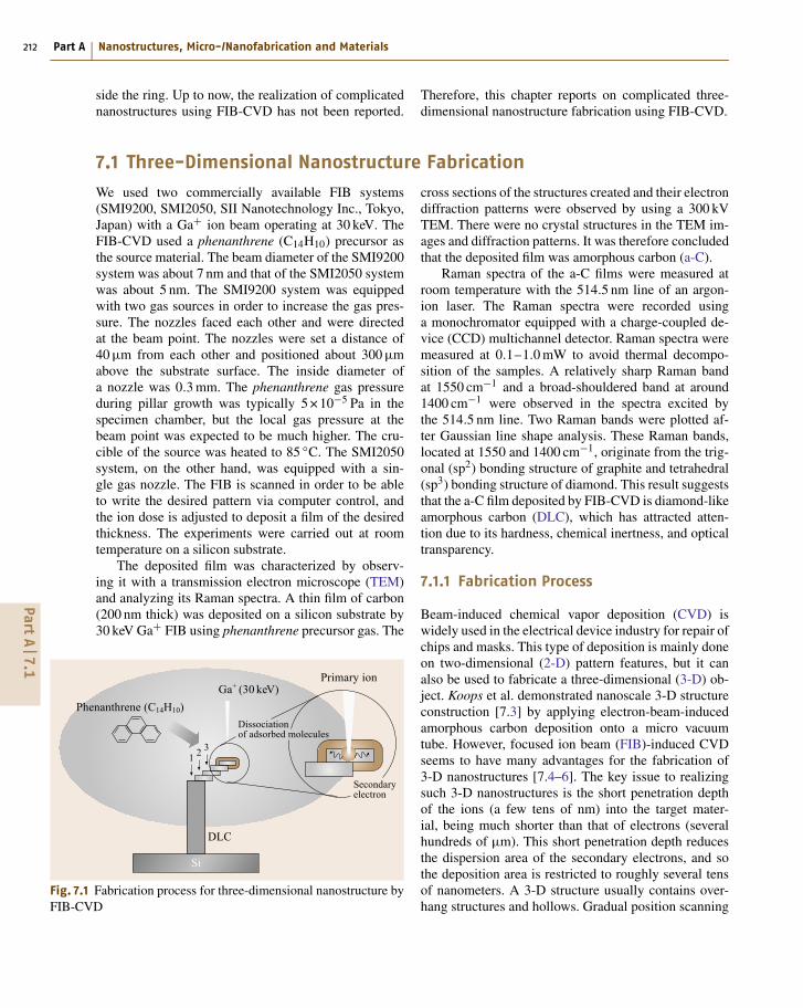
We used two commercially available FIB systems(SMI9200, SMI2050, SII Nanotechnology Inc., Tokyo,Japan) with a Ga+ ion beam operating at 30 keV. TheFIB-CVD used a phenanthrene (C14H10) precursor asthe source material. The beam diameter of the SMI9200system was about 7 nm and that of the SMI2050 systemwas about 5 nm. The SMI9200 system was equippedwith two gas sources in order to increase the gas pres-sure. The nozzles faced each other and were directedat the beam point. The nozzles were set a distance of40 μm from each other and positioned about 300 μmabove the substrate surface. The inside diameter ofa nozzle was 0.3 mm. The phenanthrene gas pressureduring pillar growth was typically 5 × 10⁻⁵ Pa in thespecimen chamber, but the local gas pressure at thebeam point was expected to be much higher. The cru-cible of the source was heated to 85 ◦C. The SMI2050system, on the other hand, was equipped with a sin-gle gas nozzle. The FIB is scanned in order to be ableto write the desired pattern via computer control, andthe ion dose is adjusted to deposit a film of the desiredthickness. The experiments were carried out at roomtemperature on a silicon substrate.
The deposited film was characterized by observ-ing it with a transmission electron microscope (TEM)and analyzing its Raman spectra. A thin film of carbon(200 nm thick) was deposited on a silicon substrate by30 keV Ga+ FIB using phenanthrene precursor gas. The
Phenanthrene (C14H10)Ga+ (30 keV)
Primary ion
Si
DLC
Dissociationof adsorbed molecules
Secondaryelectron
1 2 3
Fig. 7.1 Fabrication process for three-dimensional nanostructure byFIB-CVD
cross sections of the structures created and their electrondiffraction patterns were observed by using a 300 kVTEM. There were no crystal structures in the TEM im-ages and diffraction patterns. It was therefore concludedthat the deposited film was amorphous carbon (a-C).
Raman spectra of the a-C films were measured atroom temperature with the 514.5 nm line of an argon-ion laser. The Raman spectra were recorded usinga monochromator equipped with a charge-coupled de-vice (CCD) multichannel detector. Raman spectra weremeasured at 0.1–1.0 mW to avoid thermal decompo-sition of the samples. A relatively sharp Raman bandat 1550 cm−1 and a broad-shouldered band at around1400 cm−1 were observed in the spectra excited bythe 514.5 nm line. Two Raman bands were plotted af-ter Gaussian line shape analysis. These Raman bands,located at 1550 and 1400 cm−1, originate from the trig-onal (sp2) bonding structure of graphite and tetrahedral(sp3) bonding structure of diamond. This result suggeststhat the a-C film deposited by FIB-CVD is diamond-likeamorphous carbon (DLC), which has attracted atten-tion due to its hardness, chemical inertness, and opticaltransparency.
7.1.1 Fabrication Process
Beam-induced chemical vapor deposition (CVD) iswidely used in the electrical device industry for repair ofchips and masks. This type of deposition is mainly doneon two-dimensional (2-D) pattern features, but it canalso be used to fabricate a three-dimensional (3-D) ob-ject. Koops et al. demonstrated nanoscale 3-D structureconstruction [7.3] by applying electron-beam-inducedamorphous carbon deposition onto a micro vacuumtube. However, focused ion beam (FIB)-induced CVDseems to have many advantages for the fabrication of3-D nanostructures [7.4–6]. The key issue to realizingsuch 3-D nanostructures is the short penetration depthof the ions (a few tens of nm) into the target mater-ial, being much shorter than that of electrons (severalhundreds of μm). This short penetration depth reducesthe dispersion area of the secondary electrons, and sothe deposition area is restricted to roughly several tensof nanometers. A 3-D structure usually contains over-hang structures and hollows. Gradual position scanning
PartA
7.1

3-D Nanostructure Fabrication by FIB-CVD 7.1 Three-Dimensional Nanostructure Fabrication 213
a) Wine glass b) Coil c) Micro Colosseum
1μm 1μm 1μm
Fig. 7.2 (a) Micro wine glass withan external diameter of 2.75 μm anda height of 12 μm. (b) Microcoil withcoil diameter of 0.6 μm, coil pitch of0.7 μm, and line width of 0.08 μm.(c) Micro Colosseum
of the ion beam during the CVD process causes theposition of the growth region around the beam pointto shift. When the beam point reaches the edge of thewall, secondary electrons appear at the side of the walland just below the top surface. The DLC then startsto grow laterally; the width of the lateral growth isalso about 80 nm. Therefore, by combining the lateralgrowth mode with rotating beam scanning, it is possibleto obtain 3-D structures with rotational symmetry, suchas a wine glass.
2.752.75μm
Fig. 7.3 Micro wine glass with an external diameter of2.75 μm and a height of 12 μm on a human hair
The process of fabricating three-dimensional struc-tures by FIB-CVD is illustrated in Fig. 7.1 [7.7]. InFIB-CVD processes, the beam is scanned in digi-tal mode. First, a pillar is formed on the substrateby fixing the beam position (position 1). After that,the beam position is moved to within a diameter ofthe pillar (position 2) and then fixed until the de-posited terrace thickness exceeds the range of the ions(a few tens of nm). This process is repeated to makethree-dimensional structures. The key point to mak-ing three-dimensional structures is to adjust the beamscan speed so that the ion beam remains within the de-posited terrace, which means that the terrace thicknessalways exceeds the range of the ions. Growth in thex- and y-directions is controlled by both beam deflec-tors. The growth in the z-direction is determined by thedeposition rate; that is, the height of the structure is pro-portional to the irradiation time when the deposition rateis constant.
We intend to open up a new field of microstructureplastic art using FIB-CVD. To demonstrate the possi-bilities of this field, a micro wine glass created on a Si
5μmμm
Fig. 7.4 Micro Leaning Tower of Pisa
PartA
7.1

214 Part A Nanostructures, Micro-/Nanofabrication and Materials
3-D CAD model Slice data Voxel data
Establishpriority
Side view
Blankingdata
Scan dataScan
Blanking
3-D patterngenerator
7 6 5 4 3 2 1
Fig. 7.5 Data flow of 3-D pattern-generating system for FIB-CVD
substrate and on a human hair as works of microstruc-ture plastic art are shown in Figs. 7.2a and 7.3. A microwine glass with an external diameter of 2.75 μm anda height of 12 μm was formed. The fabrication time was600 s at a beam current of 16 pA. This beautiful microwine glass shows the potential of the field of microstruc-ture plastic art. A micro Colosseum and a micro LeaningTower of Pisa were also fabricated on a Si substrate, asshown in Figs. 7.2c and 7.4.
Various microsystem parts have been fabricated us-ing FIB-CVD. Figure 7.2b shows a microcoil with a coildiameter of 0.6 μm, a coil pitch of 0.7 μm, and a linewidth of 0.08 μm. The exposure time was 40 s at a beamcurrent of 0.4 pA. The diameter, pitch, and height ofthe microcoil were 0.25, 0.20, and 3.8 μm, respec-tively. The exposure time was 60 s at a beam currentof 0.4 pA. The results show that FIB-CVD is a highlypromising technique for realizing parts of a microsys-tem, although their mechanical performance must bemeasured.
a) 3-D CAD-model b) SIM image (tilt 45°)
1μmμm
Fig. 7.6a,b Micro Starship Enterprise NCC-1701D, 8.8 μm long
7.1.2 Three-DimensionalPattern-Generating System
We used ion-beam-assisted deposition of a source gasto fabricate 3-D structures. The 3-D structure is builtup as a multilayer structure. In the first step of this 3-Dpattern-generating system, a 3-D model of the structure,designed using a 3-D computer-aided design (CAD)system (3-D DXF format), is needed. In this case werealized a structure shaped like a pendulum. The 3-DCAD model, which is a surface model, is cut into sev-eral slices, as shown in Fig. 7.5. The thickness of theslices depends upon the resolution in the z-direction(the vertical direction). The x- and y-coordinates ofthe slices are then used to create the scan data (voxeldata). To fabricate the overhanging structure, the ionbeam must irradiate the correct positions in the cor-rect order. If the ion beam irradiates a voxel located inmid-air without a support layer, the ions intended forthe voxel will be deposited on the substrate. Therefore,
1μmμm
Fig. 7.7 T-4 bacteriophage
PartA
7.1

3-D Nanostructure Fabrication by FIB-CVD 7.2 Nanoelectromechanics 215
the sequence of irradiation is determined, as shown inFig. 7.5.
The scan data and blanking signal therefore includethe scan sequence, the dwell time, the interval time, andthe irradiation pitch. These parameters are calculatedfrom the beam diameter, xy-resolution, and z-resolutionof fabrication. The z-resolution is proportional to thedwell time and inversely proportional to the square ofthe irradiation pitch. The scan data are passed to thebeam deflector of the FIB-CVD, as are the blankingdata. The blanking signal controls the dwell time andinterval time of the ion beam.
Figure 7.6 shows a 3-D CAD model and anscanning ion microscope (SIM) image of the star-
ship Enterprise NCC-1701D (from the television seriesStar Trek), which was fabricated by FIB-CVD at10 ∼ 20 pA [7.8]. The nanospaceship is 8.8 μm longand was realized at about 1 : 100 000 000 scale onsilicon substrate. The dwell time (td), interval time(ti), irradiation pitch (p), and total process time (tp),were 80 μs, 150 μs, 2.4 nm, and 2.5 h, respectively.The horizontal overhang structure was successfullyfabricated.
Figure 7.7 shows a nano T4 bacteriophage, whichis an artificial version of the virus fabricated by FIB-CVD on silicon surface. The size of the artificial nanoT4 bacteriophage is about ten times that of the realvirus.
7.2 Nanoelectromechanics
7.2.1 Measuring Young’s Modulus
An evaluation of the mechanical characteristics of suchnanostructures is needed for material physics. Buks andRoukes reported a simple but useful technique [7.9] formeasuring the resonant frequencies of nanoscale ob-jects using a scanning electron microscope (SEM). Thesecondary electron detector in the SEM can detect fre-quencies up to around 4 MHz, so the sample vibrationis measured as the oscillatory output signal of the de-tector. Buks and Roukes used this technique to evaluatethe Casimir attractive force between two parallel beamsfabricated on a nanoscale. We evaluated the mechanicalcharacteristics of DLC pillars in terms of the Young’s
Secondaryelectrondetector
Electronbeam
Sampleholder
Piezo
Oscilloscope
Spectrumanalyzer
Driving oscillator
a) b)
Fig. 7.8 (a) SEM image of the vi-bration. The resonant frequency was1.21 MHz. (b) Schematic diagram ofthe vibration monitoring system
modulus, determined using resonant vibration and theSEM monitoring technique [7.10, 11].
The system setup for monitoring mechanical vi-bration is shown in Fig. 7.8b. There were two waysof measuring the pillar vibrations. One is active mea-surement, where the mechanical vibration is inducedby a thin piezoelectric device, 300 μm thick and 3 mmsquare. The piezo device was bonded to the sidewall ofthe SEM’s sample holder with silver paste. The sam-ple holder was designed to observe cross sections inthe SEM (S5000, Hitachi) system. Therefore, the pil-lar’s vibration was observed as a side-view image, asshown in Fig. 7.8a. The range of vibration frequenciesinvolved was 10 kHz up to 2 MHz, which is much faster Part
A7.2

216 Part A Nanostructures, Micro-/Nanofabrication and Materials
than the SEM raster scanning speed. Thus the resonantvibrations of the pillars can be taken as the trace of thepillar’s vibration in the SEM image. The resonant fre-quency and amplitude were controlled by adjusting thepower of the driving oscillator.
The other way to measure pillar vibrations is pas-sive measurement using a spectrum analyzer (Agilent4395A), where most of the vibration seemed to de-rive from environmental noise from rotary pumps andair conditioners. Some parts of the vibration resultfrom spontaneous vibration associated with thermal ex-citations [7.9]. Because of the excitation and residualnoise, the pillars on the SEM sample holder alwaysvibrated at a fundamental frequency, even if noise iso-lation is enforced on the SEM system. The amplitude ofthese spontaneous vibrations was on the order of a fewnanometers at the top of the pillar, and high-resolutionSEM can easily detect it at a magnification of 300 000.
We arranged several pillars with varying diametersand lengths. The DLC pillars with the smallest diameterof 80 nm were grown using point irradiation. While weused two FIB systems for pillar fabrication, slight dif-ferences in the beam diameters of the two systems didnot affect the diameters of the pillars. Larger-diameterpillars were fabricated using an area-limited raster scanmode. Raster scanning of a 160 nm2 region produceda pillar with a cross section of about 240 nm2, anda 400 nm2 scan resulted in a pillar with a cross sec-tion of 480 nm2. A typical SEM image taken duringresonance is shown in Fig. 7.8a. The FIB-CVD pillarsseemed very durable against mechanical vibration. Thiskind of measurement usually requires at least 30 min,including spectrum analysis and photo recording, butthe pillars still survived without any change in reso-nance characteristics. This durability of the DLC pillarsshould be useful in nanomechanical applications.
The resonant frequency f of the pillar is definedby (7.1) for a pillar with a square cross section, and (7.2)for a circular cross section
fsquare = aβ2
2πL2
√E
12ρ, (7.1)
fcircular = aβ2
2πL2
√E
16ρ, (7.2)
where a is the width of the square pillar or the diameterof the circular-shaped pillar, L is the length of the pil-lar, ρ is the density, and E is the Young’s modulus. Thecoefficient β defines the resonant mode; β = 1.875 forthe fundamental mode. We used (7.1) for pillars 240 and480 nm wide, and (7.2) for pillars grown by point-beam
irradiation. The relationship of the resonant frequencyto the Young’s modulus, which depends on the ratio ofthe pillar diameter to the squared length, is summarizedin Fig. 7.9. All of the pillars evaluated in this figure werefabricated using the SMI9200 FIB system under rapidgrowth conditions. Typical growth rates were about3–5 μm/min for the 100 nm-diameter and 240 μm-widepillars, and 0.9 μm/min for the 480 nm-wide pillars.When calculating the data shown in Fig. 7.9, we as-sumed that the density of the DLC pillars was about2.3 g/cm3, which is almost identical to that of graphiteand quartz. The slope of the line in Fig. 7.9 indicatesthe Young’s modulus for each pillar. The Young’s mod-uli of the pillars were distributed over a range from 65to 140 GPa, which is almost identical to that of nor-mal metals. Wider pillars tended to have larger Young’smoduli.
We found that the stiffness increases significantly asthe local gas pressure decreases, as shown in Fig. 7.10.While the absolute value of the local gas pressure at thebeam point is very difficult to determine, we found thatthe growth rate can be a useful parameter for describingthe dependence of Young’s modulus on pressure. Alldata points indicated in Fig. 7.10 were obtained frompillars grown using point irradiation. Therefore, the pil-lar diameters did vary slightly from 100 nm but not bymore than 5%. A relatively low gas pressure, with gooduniformity, was obtained by using a single gas nozzleand gas reflector. We used a cleaved side-wall of an Sitip as the gas reflector, which was placed 10–50 μmaway from the beam point so as to face the gas noz-zle. The growth rate was controlled by changing thedistance to the wall. While there is a large distribu-
00
a/L2 (× 10–3)
Resonant frequency (kHz)
1000
2000
3000
4000
41 2 3
E = 140 GPa E = 100 GPa
E = 650 GPa
∅ = 0.24μm∅ = 0.1μm
∅ = 0.48μm
Fig. 7.9 Dependence of resonant frequency on pillarlength
PartA
7.2

3-D Nanostructure Fabrication by FIB-CVD 7.2 Nanoelectromechanics 217
00
Growth rate (μm/min)
0.3 pA0.4 pA
Young's modulus (GPa)
1.0 pA
200
400
600
800
1000
51 2 3 4
Fig. 7.10 Dependence of Young’s modulus on growth rate
tion of data points, the stiffness of the pillar tendedto become stiffer as the growth rate decreased. Thetwo curves in Fig. 7.10 represent data points obtainedfor a beam current of 0.3 and 1 pA, respectively. Bothcurves show the same tendency; the saturated upper lev-els of the Young’s modulus are different for each ioncurrent at low gas pressure (low growth rate). It shouldbe noted that some of the pillars’ Young’s moduli ex-ceeded 600 GPa, which is of the same order as thatof tungsten carbide. In addition, these estimations as-sume a pillar density of 2.3 g/cm3, but a finite amountof Ga was incorporated with the pillar growth. If thecalculation takes the increase in pillar density due tothe Ga concentration into account, the Young’s mod-ulus exceeds 800 GPa. Such a high Young’s modulusreaches that of carbon nanotubes and natural diamondcrystals. We think that this high Young’s modulus is dueto surface modification caused by the direct ion impact.
Ga+ FIBBeam scanning direction
Source gas
Wall
3-D nanowiringgrowth direction
1μmμm
Faster
Slower Fig. 7.11 Fabrication of DLC free-space wiring using both FIB-CVDand CPG
In contrast, when the gas pressure was high enoughto achieve a growth rate of more than 3 μm/min, the pil-lars became soft but the change in the Young’s moduluswas small. The uniformity of the Young’s modulus (asseen in Fig. 7.9) presumably results from the fact thatthe growth occurred in this insensitive region, where thelow levels of source gas limit pillar growth.
7.2.2 Free-Space Nanowiring
All experiments were carried out in a commerciallyavailable FIB system (SMI9200: SII NanoTechnologyInc.) using a beam of 30 kV Ga+ ions. The beam wasfocused to a spot size of 7 nm at a beam current of0.4 pA, and it was incident perpendicular to the surface.The pattern drawing system (CPG-1000: Crestec Co.,Tokyo) was added to the FIB apparatus to draw any pat-terns. Using the CPG, it is possible to control beam scanparameters such as scanning speed, xy-direction, andblanking of the beam, and so 3-D free space nanowiringcan be performed [7.12].
Figure 7.11 illustrates the free-space nanowiringfabrication process using both FIB-CVD and CPG.When phenanthrene (C14H10) gas or tungsten hexacar-bonyl (W(CO)6) gas, which is a reactive organic gas,is evaporated from a heated container and injected intothe vacuum chamber by a nozzle located 300 μm abovethe sample surface at an angle of about 45◦ with respectto surface, the gas density of the C14H10 or W(CO)6molecules increases on the substrate near the gas noz-zle. The nozzle system creates a local high-pressureregion over the surface. The base pressure of the sam-ple chamber is 2 × 10⁻⁵ Pa and the chamber pressureupon introducing C14H10 and W(CO)6 as a source gaswas 1 × 10⁻⁴ and 1.5 × 10⁻³ Pa, respectively. If a Ga+
PartA
7.2

218 Part A Nanostructures, Micro-/Nanofabrication and Materials
ion beam is irradiated onto the substrate, C14H10 orW(CO)6 molecules adsorbed on the substrate surfaceare decomposed, and carbon (C) is mainly depositedonto the surface of the substrate. The direction of depo-sition growth can be controlling through the scanningdirection of the beam. The material deposited usingC14H10 gas was diamond-like carbon, as confirmed byRaman spectra, and it had a very large Young’s modulusof 600 GPa [7.7, 10].
After the two walls shown in Fig. 7.11 were formed,free-space nanowiring was performed by adjusting thebeam scanning speed. The ion beam used was a 30 kVGa+ FIB, and the irradiation current was 0.8–2.3 pA.The x- and y-scanning directions and the beam scan-ning speed were controlled by the CPG. The height inthe z-direction was proportional to the irradiation time.Deposition is made to occur horizontally by scanning
11μmμm
1μmμm8080 nmnm
8080 nmnm
b)
a)
Fig. 7.12 (a) DLC free-space wiring with a bridge shape.(b) DLC free-space wiring with parallel resistances
a) b)
11μmμm 1μmμm
Fig. 7.13 (a) Radial DLC free-space wiring grown in 16 directionsfrom the center. (b) Scanning ion microscope (SIM) micrograph ofinductance (L), resistance (R), and capacitor (C) structure
the beam at a certain fixed speed in a plane. How-ever, if the beam scanning speed is faster than thenanowiring growth speed, it grows downward or drops;conversely, if the scanning speed is too slow, the de-position grows slanting upward. Therefore, it is veryimportant to control the beam scanning speed care-fully when growing a nanowire horizontally. It turnsout that the optimal beam scanning speed to realizea nanowire growing horizontally, using two C14H10 gasguns, was about 190 nm/s. The expected pattern resolu-tion archived using FIB-CVD is around 80 nm, becauseboth the primary Ga+ ion and secondary-electron scat-tering occur over distances of around 20 nm [7.10, 13].
Figures 7.12 and 7.13 show examples of free-spacenanowiring fabricated by FIB-CVD and CPG. All ofthe structures shown were fabricated using C14H10 asa precursor gas.
Figure 7.12a shows nanobridge free-space wiring.The growth time was 1.8 min and the wiring width was80 nm. Figure 7.12b shows free-space nanowires withparallel resistances. The growth time was 2.8 min, andthe wiring width was also 80 nm.
Figure 7.13a shows free-space nanowiring grownin 16 directions from the center. Figure 7.13b showsa scanning ion microscope (SIM) image of an induc-tor (L), a resistor (R), and a capacitor (C) in a parallelcircuit structure with free-space nanowiring. A coiledstructure was fabricated by circle-scanning of the Ga+FIB. The growth times of the L, R, and C structureswere about 6, 2, and 12 min, and all the nanowiring isabout 110 nm wide. From these structures, one can seethat it is possible to fabricate nanowiring at an arbitraryposition using FIB-CVD and CPG. These results alsoindicate that various circuit structures can be formed bycombining L, C, and R.
The free-space wiring structures were observed us-ing 200 keV TEM. The analyzed area was 20 nm indiameter. Figure 7.14a,b shows TEM images of DLCfree-space wiring and a pillar. It became clear fromthese energy-dispersive x-ray (EDX) measurements thatthe dark part (A) of Fig. 7.14a corresponds to the Gacore, while the outside part (B) of Fig. 7.14a corre-sponds to amorphous carbon. This free-space wiringtherefore consists of amorphous carbon with a Ga core.The center position of the Ga core is actually locatedbelow the center of the wiring. However, in the case ofthe DLC pillar, the Ga core is located at the center of thepillar. To investigate the difference between these corepositions, the Ga core distribution in free-space wiringwas observed in detail by TEM. The center position ofthe Ga core was about 70 nm from the top, which was
PartA
7.2
3-D Nanostructure Fabrication by FIB-CVD 7.2 Nanoelectromechanics 219
100 nm
100100 nmnm
(B)
(A)
DLC free-space wiringa)
DLC pillarb)
Fig. 7.14a,b TEM images of (a) DLC free-space wiringand (b) DLC pillar
20 nm below the center of the free-space wiring. Wecalculated an ion range of 30 kV Ga ions into amor-phous carbon, using transport of ions in matter (TRIM),of 20 nm. The calculation indicates that the displace-ment of the center of the Ga core in the nanowiringcorresponds to the ion range.
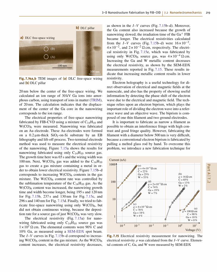
The electrical properties of free-space nanowiringfabricated by FIB-CVD using a mixture of C14H10 andW(CO)6 were measured. Nanowiring was fabricatedon an Au electrode. These Au electrodes were formedon a 0.2 μm-thick SiO2-on-Si substrate by an EBlithography and lift-off process. Two-terminal electrodemethod was used to measure the electrical resistivityof the nanowiring. Figure 7.15a shows the results fornanowiring fabricated using only C14H10 source gas.The growth time here was 65 s and the wiring width was100 nm. Next, W(CO)6 gas was added to the C14H10gas to create a gas mixture containing a metal in or-der to obtain lower electrical resistivity. Figure 7.15b–dcorresponds to increasing W(CO)6 contents in the gasmixture. The W(CO)6 content rate was controlled bythe sublimation temperature of the C14H10 gas. As theW(CO)6 content was increased, the nanowiring growthtime and width become longer, being 195 s and 120 nmfor Fig. 7.15b, 237 s and 130 nm for Fig. 7.15c, and296 s and 140 nm for Fig. 7.15d. Finally, we tried to fab-ricate free-space nanowiring using only W(CO)6, butdid not obtain continuous wiring, because the deposi-tion rate for a source gas of just W(CO)6 was very slow.
The electrical resistivity (Fig. 7.15a) for nano-wiring fabricated using only C14H10 source gas was1 × 102 Ω cm. The elemental contents were 90% C and10% Ga, as measured using a SEM-EDX spot beam.The I–V curves in Fig. 7.15b–d correspond to increas-ing W(CO)6 content in the gas mixture. As the W(CO)6content increases, the electrical resistivity decreases,
as shown in the I–V curves (Fig. 7.15b–d). Moreover,the Ga content also increased because the growth ofnanowiring slowed; the irradiation time of the Ga+ FIBbecame longer. The electrical resistivities calculatedfrom the I–V curves (Fig. 7.15b–d) were 16 × 10−2,4 × 10−2, and 2 × 10⁻² Ω cm, respectively. The electri-cal resistivity in Fig. 7.15e, which was fabricated byusing only W(CO)6 source gas, was 4 × 10⁻⁴ Ω cm.Increasing the Ga and W metallic content decreasesthe electrical resistivity, as shown by the SEM-EDXmeasurements reported in Fig. 7.15. These results in-dicate that increasing metallic content results in lowerresistivity.
Electron holography is a useful technology for di-rect observation of electrical and magnetic fields at thenanoscale, and also has the property of showing usefulinformation by detecting the phase shift of the electronwave due to the electrical and magnetic field. The tech-nique relies upon an electron biprism, which plays theimportant role of dividing the electron wave into a refer-ence wave and an objective wave. The biprism is com-posed of one thin filament and two ground electrodes.
It is important to fabricate as narrow a filament aspossible to obtain an interference fringe with high con-trast and good fringe quality. However, fabricating thefilament with a diameter below 500 nm is very difficult,because a conventional electron biprism is fabricated bypulling a melted glass rod by hand. To overcome thisproblem, we introduce a new fabrication technique for
10–4 10110010–110–210–3
Current (nA)
(e)ρ = 4×10⁻⁴ Ω cmC = 22%Ga = 25%W = 53%
(d)ρ = 2×10⁻²Ω cmC = 74%Ga = 19%W = 7%
(b)ρ = 16 Ω cmC = 85%Ga = 13%W = 2%
(a)ρ = 100 Ω cm
C = 90 %Ga = 10 %
W = 0 %
(c)ρ = 4 ×10⁻²Ω cmC = 78%Ga = 18%W = 4%
1000
100
10
1
Voltage (V)
Fig. 7.15 Electrical resistivity measurement for nanowiring. Theelectrical resistivity ρ was calculated from the I–V curve. Elemen-tal contents of C, Ga, and W were measured by SEM-EDX
PartA
7.2

220 Part A Nanostructures, Micro-/Nanofabrication and Materials
10 µmµm
Fig. 7.16 Electron biprism fabricated by FIB-CVD
the electron biprism using FIB-CVD, and evaluate thecharacteristics of the new biprism [7.14].
Figure 7.16 shows an SEM micrograph of the FIB-CVD biprism. We successfully fabricated DLC wiringwith a smooth surface in between W rods by free-spacewiring fabrication based on FIB-CVD technology. The80 nm DLC thin wiring works as the filament of thebiprism. The diameter and length of the filament are80 nm and 15 μm, respectively.
Figure 7.17 shows interference fringes obtained us-ing the biprism with a filament of 80 nm diameter(Fig. 7.17a) and 400 nm diameter (Fig. 7.17b), and cor-
0 50 100 150 200 250 300 350
Interference region (nm)
3
2.5
2
1.5
1
0.5
a)
0 50 100 150 200 250 300 350
Interference region (nm)
Intensity (au)
Intensity (au)3
2.5
2
1.5
1
0.5
b)
Fig. 7.17a,b Interference fringes and corresponding fringe profiles. (a) Obtained using the biprism with diameter of80 nm, and (b) obtained using the biprism with diameter of 400 nm
responding fringe profiles. The applied prism voltagewas 20 V, respectively. The filament with 400 nm diam-eter, close to the standard size used in the conventionalelectron biprism, was fabricated by Pt sputter-coatingonto the 80 nm-diameter filament. Interference fringeswere successfully obtained. Moreover, the interferenceregion of the fringe obtained using the biprism with the80 nm-diameter filament is larger than that of the fringeobtained using the biprism with the 400 nm-diameterfilament. These results demonstrate the adequacy ofthe thin filament fabricated by FIB-CVD, and the newbiprism will be very useful for accurate observationwith high contrast and good fringe quality in electronholography.
7.2.3 Nanomechanical Switch
We have also demonstrated a nanomechanical switchfabricated by FIB-CVD [7.15]. Figure 7.18a showsthe principle behind the realization of a nanomechan-ical switch. First, an Au electrode was formed on
PartA
7.2

3-D Nanostructure Fabrication by FIB-CVD 7.2 Nanoelectromechanics 221
a 0.2 μm-thick SiO2-on-Si substrate by an electron-beam lithography and lift-off process. After that, a coiland free-space nanowiring were fabricated onto the Auelectrode to form a switch function using nanowiringfabrication technology with FIB-CVD and CPG. Thecoil structure was fabricated by scanning a Ga+ beamin a circle at fixed speed in C14H10 ambiance gas. Anelectric charge (positive or negative) was applied tothe coil, and the reverse electric charge was appliedto the nanowiring. The coil extended upward whena voltage was applied, because these was now an elec-trical repulsive force between each loop of the coil.At the same time, the coil and the nanowiring grav-itated toward one another, because they had oppositecharges. This attraction caused the coil to contact withthe nanowiring when a certain threshold voltage wasreached.
Next, we evaluated the switch function by mea-suring the current that flowed when the coil and thenanowiring were in contact. Figure 7.18b,c shows SIMmicrographs of the nanomechanical switch before andafter applying a voltage. These micrographs indicatethat the coil and nanowiring make contact when a volt-age is applied to the coil. At the same time, I–Vmeasurements of the nanomechanical switch were car-ried out, as shown in Fig. 7.19a. The current was plottedagainst the applied voltage at room temperature, andfrom this graph, it was apparent that the current be-gins to flow at a threshold voltage of 17.6 V. At thispoint, the electrical resistance and the resistivity of thenanomechanical switch are about 250 MΩ and 11 Ω cm,respectively. We measured the I–V characteristics forten nanomechanical switches. The threshold voltagewas around 20 V in each case. The switching functionwas confirmed by performing on/off operations at an ap-
00
Current (nA)
160
20
40
60
80
100
120
140
305 10 15 20 25Voltage (V)
00
Current (nA)
250
Time (s)
50
100
150
200
82 4 6
a) b)
Fig. 7.19 (a) I–V curve for thenanomechanical switch. (b) Pulsedcurrent to on/off operation for thenanomechanical switch at an appliedvoltage of 30 V
SiO2Au
a)
b) c)
1μmμm 1μmμm
Fig. 7.18 (a) Principle of movement of nanomechanical switch.SIM micrographs of nanomechanical switch: (b) before applyingvoltage and (c) after applying voltage
plied voltage of 30 V, as shown in Fig. 7.19b. A pulsedcurrent of about 170 nA was detected for this appliedvoltage.
7.2.4 Nanoelectrostatic Actuator
The fabrication process of 3-D nanoelectrostatic ac-tuators (and manipulators) is very simple [7.16]. Fig-ure 7.20 shows the fabrication process. First, a glasscapillary (GD-1: Narishige Co., East meadow, NY) waspulled using a micropipette puller (PC-10: NarishigeCo.). The dimensions of the glass capillary were 90 mmin length and 1 mm in diameter. Using this process,
PartA
7.2

222 Part A Nanostructures, Micro-/Nanofabrication and Materials
III. 3-D structure fabrication by FIB-CVD
I. Pulling
II. Au surface coating
Au(electrode)
Gas nozzle
Phenanthrene gas
Ga+ FIB
Diamond-like carbon
Glass capillary
Glass capillary
Fig. 7.20 Fabrication process of 3-D nanoelectrostatic actuators
we obtained a glass capillary tip with a 1 μm diam-eter. Next, we coated the glass capillary surface withAu by direct-current (DC) sputtering. The Au thicknesswas ≈ 30 nm. This Au coating serves as the electrodethat controls the actuator and manipulator. Then, the3-D nanoelectrostatic actuators and manipulators werefabricated by FIB-CVD. This process was carried outin a commercially available FIB system (SIM9200: SIINanoTechnology Inc.) with a Ga+ ion beam operatingat 30 keV. FIB-CVD was carried out using a phenan-threne (C14H10) precursor as the source material. Thebeam diameter was about 7 nm. The inner diameter ofeach nozzle was 0.3 mm. The phenanthrene gas pres-sure during growth was typically 5 × 10⁻⁵ Pa in thespecimen chamber. The Ga+ ion beam was controlledby transmitting CAD data on the arbitrary structures tothe FIB system.
00
Voltage (V)
Bending distance a (μm)
0.2
0.4
0.6
0.8
1
1.2
1.4
1500250 500 750 1000 1250
10μmμm
0 V 15001500 V
a
10μmμm
Fig. 7.22 Dependence of bending distance on applied voltage
a) SIM image b) Moving principle
1μmμm
Fig. 7.21a,b Laminated pleats-type electrostatic actuator.(a) SIM image of a laminated pleats-type electrostatic ac-tuator fabricated on the tip of a Au-coated glass capillary.(b) Illustration of moving principle of the actuator
A laminated pleats-type electrostatic actuator wasfabricated by FIB-CVD. Figure 7.21a shows an SIMimage of a laminated pleats-type electrostatic actuatorfabricated at 7 pA and 60 min exposure time. Fig-ure 7.21b shows the principle behind the movement ofthis actuator. The driving force is the repulsive forcedue to the accumulation of electric charge. This elec-tric charge can be stored in the pleats structures of theactuator by applying a voltage across the glass capil-lary. The pillar structure of this actuator bends due tocharge repulsion, as shown in Fig. 7.21b. Figure 7.22shows the dependence of the bending distance on the
a) SIM image b) Moving principle
1μmμm
Fig. 7.23a,b Coil-type electrostatic actuator. (a) SIM im-age of a coil-type electrostatic actuator fabricated on thetip of a Au-coated glass capillary. (b) Illustration of movingprinciple for the actuator
PartA
7.2

3-D Nanostructure Fabrication by FIB-CVD 7.3 Nanooptics: Brilliant Blue Observation from a Morpho Butterfly Scale Quasistructure 223
applied voltage. The bending distance is defined as thedistance a in the inset of Fig. 7.22. The bending rateof this laminated pleats-type electrostatic actuator wasabout 0.7 nm/V.
A coil-type electrostatic actuator was fabricatedby FIB-CVD. Figure 7.23a shows an SIM image ofa coil-type electrostatic actuator fabricated at 7 pA and10 min of exposure time. Figure 7.23b shows the prin-ciple behind the movement of this actuator, which isvery simple. The driving force is the repulsive forceinduced by electric charge accumulation; the electriccharge can be stored in this coil structure by applyinga voltage across the glass capillary. This coil struc-ture expands and contracts due to charge repulsion,as shown in Fig. 7.23b. Figure 7.24 shows the depen-dence of the coil expansion on the applied voltage. Thelength of the expansion is the distance a in the inset ofFig. 7.24. The result revealed that the expansion could
02
Voltage applied (V)
Expansion a (μm)
2.5
3
3.5
500100 200 300 400
a
1μmμm 1μmμm
0 V 500500 V
Fig. 7.24 Dependence of coil expansion on applied voltage
be controlled in the applied voltage range from 0 to500 V.
7.3 Nanooptics: Brilliant Blue Observationfrom a Morpho Butterfly Scale Quasistructure
The Morpho butterfly has brilliant blue wings, and thesource of this intense color has been an interesting topicof debate for a long time. Due to an intriguing opti-cal phenomenon, the scales reflect interfered brilliantblue color for any angle of incidence of white light.This color is called a structural color, meaning that it isnot caused by pigment reflection [7.17]. When we ob-served the scales with a scanning electron microscope(SEM) (Fig. 7.25a), we found three-dimensional (3-D)nanostructures 2 μm in height, 0.7 μm in width, andwith a 0.22 μm grating pitch on the scales. These nano-structures cause a similar optical phenomenon to theiridescence produced by a jewel beetle.
We duplicated the Morpho butterfly scale qua-sistructure with a commercially available FIB system(SMI9200: SII Nanotechnology Inc.) using a Ga+ ionbeam operating at 30 kV [7.18]. The beam diameter wasabout 7 nm at 0.4 pA. The FIB-CVD was performedusing phenanthrene (C14H10) as a precursor.
In this experiment, we used a computer-controlledpattern generator, which converted 3-D computer-aideddesign (CAD) data into a scanning signal, which waspassed to an FIB scanning apparatus in order to fabri-cate a 3-D mold [7.8]. The scattering range of the Gaprimary ions is about 20 nm, and the range of the sec-ondary electrons induced by the Ga ion beam is about
20 nm, so the expected pattern resolution of the FIB-CVD is about 80 nm.
Figure 7.25b shows an SIM image of the Morphobutterfly quasistructure fabricated by FIB-CVD using 3-
Shetener Morphoa) b)
1μmμm
Fig. 7.25a,b Morpho butterfly scales. (a) Optical microscope imageshowing top view of Morpho butterfly. SEM image showing a cross-sectional view of Morpho butterfly scales. (b) SIM image showinginclined view of Morpho butterfly scale quasistructure fabricated byFIB-CVD
PartA
7.3

224 Part A Nanostructures, Micro-/Nanofabrication and Materials
D CAD data. This result demonstrates that FIB-CVDcan be used to fabricate the quasistructure.
We measured the reflection intensities from Morphobutterfly scales and the Morpho butterfly scale qua-sistructure optically; white light from a halogen lampwas directed onto a sample with angles of incidenceranging from 5◦ to 45◦. The reflection was concentratedby an optical microscope and analyzed using a commer-cially available photonic multichannel spectral analyzersystem (PMA-11: Hamamatsu Photonics K.K., Hama-matsu City, Japan). The intensity of light incident fromthe halogen lamp had a peak at a wavelength closeto 630 nm.
The Morpho butterfly scale quasistructure was madeof DLC. The reflectivity and transmittance of a 200 nm-thick DLC film deposited by FIB-CVD, measured bythe optical measurement system at a wavelength close to440 nm (the reflection peak wavelength of the Morphobutterfly), were 30% and 60%, respectively. Therefore,the measured data indicated that the DLC film hadhigh reflectivity near 440 nm, which is important forthe fabrication of an accurate Morpho butterfly scalequasistructure.
We measured the reflection intensities of theMorpho butterfly scales and the quasistructure withan optical measurement system, and compared theircharacteristics. Figure 7.26a,b shows the reflectionintensities from Morpho butterfly scales and the qua-sistructure, respectively. Both gave a peak intensity near440 nm and showed very similar reflection intensityspectra for various angles of incidence.
We have thus successfully demonstrated that a Mor-pho butterfly scale quasistructure fabricated using
3500
Wavelength (nm)
Intensity (arb. units)
0.2
0.4
0.6
0.8
1a)
850400 450 500 550 600 650 700 750 800
30°
5°20°
Incident angle
3500
Wavelength (nm)
Intensity (arb. units)
0.2
0.4
0.6
0.8
1b)
850400 450 500 550 600 650 700 750 800
Fig. 7.26a,b Intensity curves of the reflection spectra for:(a) Morpho butterfly scales, (b) Morpho butterfly scale qua-sistructure
FIB-CVD can give almost the same optical character-istics as real Morpho butterfly scales.
7.4 Nanobiology
7.4.1 Nanoinjector
Three-dimensional nanostructures on a glass capillaryhave a number of useful applications, such as manipu-lators and sensors in various microstructures. We havedemonstrated the fabrication of a nozzle nanostructureon a glass capillary for a bioinjector using 30 keV Ga+focused ion beam assisted deposition with a precur-sor of phenanthrene vapor and etching [7.19]. It hasbeen demonstrated that nozzle nanostructures of vari-ous shapes and sizes can be successfully fabricated. Aninner tip diameter of 30 nm on a glass capillary and a tipshape with an inclined angle have been realized. We re-
ported that diamond-like carbon (DLC) pillars grownby FIB-CVD with a precursor of phenanthrene vaporhave very large Young’s moduli, exceeding 600 GPa,which potentially makes them useful for various appli-cations [7.10]. These characteristics are applicable tothe fabrication of various biological devices.
In one experiment, nozzle nanostructure fabricationfor biological nanoinjector research was studied. The tipdiameters of conventional bioinjectors are greater than100 nm and the tip shapes cannot be controlled. A bio-nanoinjector with various nanostructures on the top ofa glass capillary has the following potential applications(shown in Fig. 7.27):
PartA
7.4
3-D Nanostructure Fabrication by FIB-CVD 7.4 Nanobiology 225
Injector
Manipulator
Cell
Sensor
Fig. 7.27 Potential uses for a bionanoinjector
1. Injection of various reagents into a specific or-ganelle in a cell
2. Selective manipulation of a specific organelle out-side of a cell by using the nanoinjector as anaspirator
3. Reducing the mechanical stress produced when op-erating in the cell by controlling the shape and sizeof the bionanoinjector
4. Measurement of the electric potential of a cell, anorganelle, and an ion channel exiting on a mem-brane, by fabricating an electrode
Thus far, 3-D nanostructure fabrications on a glasscapillary have not been reported. We present nozzlenanostructure fabrication on a glass capillary by FIB-CVD and etching in order to confirm the possibility ofbionanoinjector fabrication.
The nozzle structures of the nanoinjector were fab-ricated using a function generator (Wave Factory: NFElectronic Instruments, Yokohama, Japan). Conven-tional microinjectors are fabricated by pulling a glasscapillary (GD-1: Narishige Co.) using a micropipettepuller (PC-10: Narishige Co.). The glass capillary was90 mm in length and 1 mm in diameter.
Tip ofip ofbio-nano bio-nano injectorinjector
a) Before b) After c) Cross section
GlassGlasscapillarycapillary
1μmμm 1μmμm 1μmμm
Fig. 7.28a–c SIM images of a bio-nanoinjector fabricated on a glasscapillary by FIB-CVD. (a) BeforeFIB-CVD, (b) after FIB-CVD, and(c) cross section of (b)
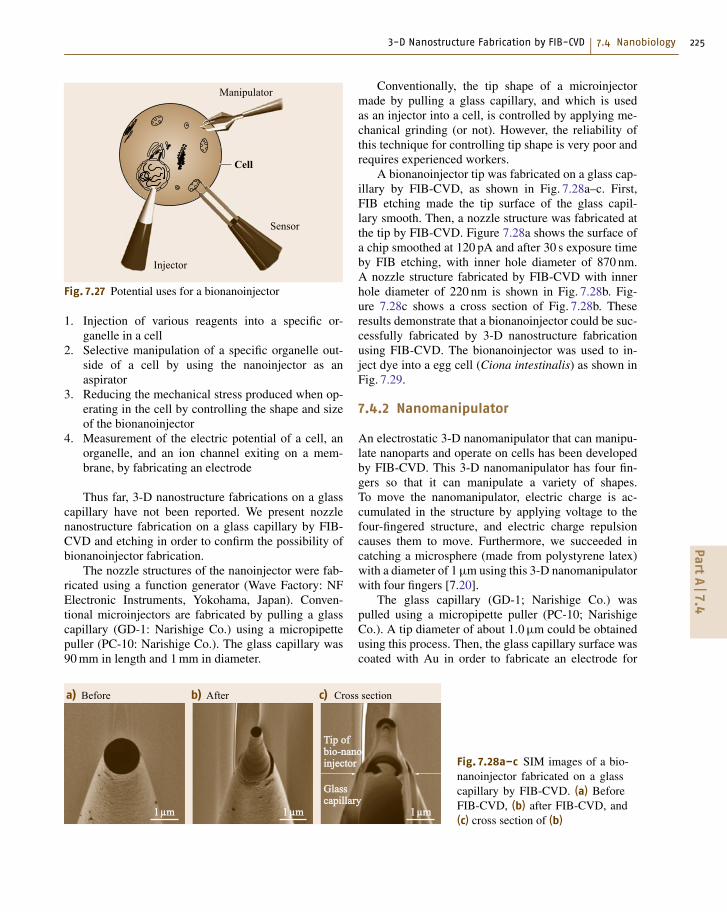
Conventionally, the tip shape of a microinjectormade by pulling a glass capillary, and which is usedas an injector into a cell, is controlled by applying me-chanical grinding (or not). However, the reliability ofthis technique for controlling tip shape is very poor andrequires experienced workers.
A bionanoinjector tip was fabricated on a glass cap-illary by FIB-CVD, as shown in Fig. 7.28a–c. First,FIB etching made the tip surface of the glass capil-lary smooth. Then, a nozzle structure was fabricated atthe tip by FIB-CVD. Figure 7.28a shows the surface ofa chip smoothed at 120 pA and after 30 s exposure timeby FIB etching, with inner hole diameter of 870 nm.A nozzle structure fabricated by FIB-CVD with innerhole diameter of 220 nm is shown in Fig. 7.28b. Fig-ure 7.28c shows a cross section of Fig. 7.28b. Theseresults demonstrate that a bionanoinjector could be suc-cessfully fabricated by 3-D nanostructure fabricationusing FIB-CVD. The bionanoinjector was used to in-ject dye into a egg cell (Ciona intestinalis) as shown inFig. 7.29.
7.4.2 Nanomanipulator
An electrostatic 3-D nanomanipulator that can manipu-late nanoparts and operate on cells has been developedby FIB-CVD. This 3-D nanomanipulator has four fin-gers so that it can manipulate a variety of shapes.To move the nanomanipulator, electric charge is ac-cumulated in the structure by applying voltage to thefour-fingered structure, and electric charge repulsioncauses them to move. Furthermore, we succeeded incatching a microsphere (made from polystyrene latex)with a diameter of 1 μm using this 3-D nanomanipulatorwith four fingers [7.20].
The glass capillary (GD-1; Narishige Co.) waspulled using a micropipette puller (PC-10; NarishigeCo.). A tip diameter of about 1.0 μm could be obtainedusing this process. Then, the glass capillary surface wascoated with Au in order to fabricate an electrode for
PartA
7.4
226 Part A Nanostructures, Micro-/Nanofabrication and Materials
Nano-injector
Cell; 100μm
Glasscapillary
Fig. 7.29 Injection into an egg cell (Ciona intestinalis) us-ing a bionanoinjector
nanomanipulator control. The thickness of the Au coat-ing was about 30 nm. Finally, a 3-D nanomanipulatorstructure with four fingers (Fig. 7.30) was fabricatedby FIB-CVD on the tip of the glass capillary with anelectrode.
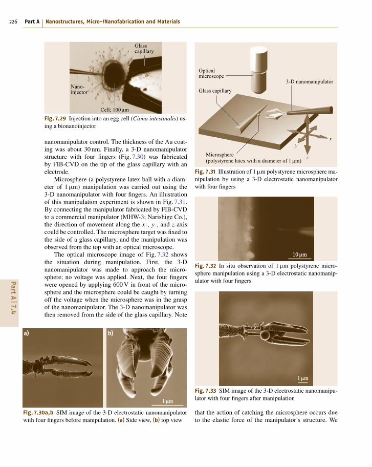
Microsphere (a polystyrene latex ball with a diam-eter of 1 μm) manipulation was carried out using the3-D nanomanipulator with four fingers. An illustrationof this manipulation experiment is shown in Fig. 7.31.By connecting the manipulator fabricated by FIB-CVDto a commercial manipulator (MHW-3; Narishige Co.),the direction of movement along the x-, y-, and z-axiscould be controlled. The microsphere target was fixed tothe side of a glass capillary, and the manipulation wasobserved from the top with an optical microscope.
The optical microscope image of Fig. 7.32 showsthe situation during manipulation. First, the 3-Dnanomanipulator was made to approach the micro-sphere; no voltage was applied. Next, the four fingerswere opened by applying 600 V in front of the micro-sphere and the microsphere could be caught by turningoff the voltage when the microsphere was in the graspof the nanomanipulator. The 3-D nanomanipulator wasthen removed from the side of the glass capillary. Note
11μmμm
a) b)
Fig. 7.30a,b SIM image of the 3-D electrostatic nanomanipulatorwith four fingers before manipulation. (a) Side view, (b) top view
Opticalmicroscope
Glass capillary
3-D nanomanipulator
Microsphere(polystyrene latex with a diameter of 1μm)
yx
z
Fig. 7.31 Illustration of 1 μm polystyrene microsphere ma-nipulation by using a 3-D electrostatic nanomanipulatorwith four fingers
110μmμm
Fig. 7.32 In situ observation of 1 μm polystyrene micro-sphere manipulation using a 3-D electrostatic nanomanip-ulator with four fingers
11μmμm
Fig. 7.33 SIM image of the 3-D electrostatic nanomanipu-lator with four fingers after manipulation
that the action of catching the microsphere occurs dueto the elastic force of the manipulator’s structure. We
PartA
7.4
3-D Nanostructure Fabrication by FIB-CVD 7.4 Nanobiology 227
succeeded in catching the microsphere, as shown in theSIM image in Fig. 7.33.
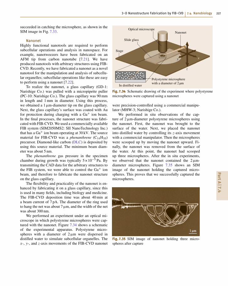
NanonetHighly functional nanotools are required to performsubcellular operations and analysis in nanospace. Forexample, nanotweezers have been fabricated on anAFM tip from carbon nanotube [7.21]. We haveproduced nanotools with arbitrary structures using FIB-CVD. Recently, we have fabricated a nanonet as a novelnanotool for the manipulation and analysis of subcellu-lar organelles; subcellular operations like these are easyto perform using a nanonet [7.22].
To realize the nanonet, a glass capillary (GD-1:Narishige Co.) was pulled with a micropipette puller(PC-10: Narishige Co.). The glass capillary was 90 mmin length and 1 mm in diameter. Using this process,we obtained a 1 μm-diameter tip on the glass capillary.Next, the glass capillary’s surface was coated with Aufor protection during charging with a Ga+ ion beam.In the final processes, the nanonet structure was fabri-cated with FIB-CVD. We used a commercially availableFIB system (SIM2050MS2: SII NanoTechnology Inc.)that has a Ga+ ion beam operating at 30 kV. The sourcematerial for FIB-CVD was a phenanthrene (C14H10)precursor. Diamond-like carbon (DLC) is deposited byusing this source material. The minimum beam diam-eter was about 5 nm.
The phenanthrene gas pressure in the specimenchamber during growth was typically 5 × 10⁻⁵ Pa. Bytransmitting the CAD data for the arbitrary structures tothe FIB system, we were able to control the Ga+ ionbeam, and therefore to fabricate the nanonet structureon the glass capillary.
The flexibility and practicality of the nanonet is en-hanced by fabricating it on a glass capillary, since thisis used in many fields, including biology and medicine.The FIB-CVD deposition time was about 40 min ata beam current of 7 pA. The diameter of the ring usedto hang the net was about 7 μm, and the width of the netwas about 300 nm.
We performed an experiment under an optical mi-croscope in which polystyrene microspheres were cap-tured with the nanonet. Figure 7.34 shows a schematicof the experimental apparatus. Polystyrene micro-spheres with a diameter of 2 μm were dispersed indistilled water to simulate subcellular organelles. Thex-, y-, and z-axis movements of the FIB-CVD nanonet
Optical microscope
Polystyrene microspherewith a diameter of 2 µm
y x
z
Nanonet
Slide glass
Stage
In distilled water
Fig. 7.34 Schematic drawing of the experiment where polystyrenemicrospheres were captured using a nanonet
were precision-controlled using a commercial manipu-lator (MHW-3; Narishige Co.).
We performed in situ observations of the cap-ture of 2 μm-diameter polystyrene microspheres usingthe nanonet. First, the nanonet was brought to thesurface of the water. Next, we placed the nanonetinto distilled water by controlling its z-axis movementwith a commercial manipulator. Then the microsphereswere scooped up by moving the nanonet upward. Fi-nally, the nanonet was removed from the surface ofthe water. At this point, the nanonet had scoopedup three microspheres. After the in situ experiments,we observed that the nanonet contained the 2 μm-diameter microspheres. Figure 7.35 shows an SIMimage of the nanonet holding the captured micro-spheres. This proves that we successfully captured themicrospheres.
11μmμm
Fig. 7.35 SIM image of nanonet holding three micro-spheres after capture
PartA
7.4

228 Part A Nanostructures, Micro-/Nanofabrication and Materials
7.5 Summary
Three-dimensional nanostructure fabrication using30 keV Ga+ FIB-CVD and a phenanthrene (C14H10)source as a precursor has been demonstrated. Thefilm deposited on a silicon substrate was characterizedusing a transmission microscope and Raman spec-tra. This characterization indicated that the depositedfilm is diamond-like amorphous carbon, which hasattracted attention due to its hardness, chemical in-ertness, and optical transparency. Its large Young’smodulus, which exceeds 600 GPa, makes it highly de-
sirable for various applications. A nanoelectrostaticactuator and 0.1 μm nanowiring were fabricated andevaluated as parts of nanomechanical system. Fur-thermore, a nanoinjector and nanomanipulator werefabricated as novel nanotools for manipulation andanalysis of subcellular organelles. These results demon-strate that FIB-CVD is one of the key technologiesneeded to make 3-D nanodevices that can be usedin the field of electronics, mechanics, optics, andbiology.
References
7.1 S. Matsui: Nanostructure fabrication using electronbeam and its application to nanometer devices,Proc. IEEE 85, 629 (1997)
7.2 O. Lehmann, F. Foulon, M. Stuke: Surface and three-dimensional processing by laser chemical vapordeposition, NATO ASI Ser. Appl. Sci. 265, 91 (1994)
7.3 H.W. Koops, J. Kretz, M. Rudolph, M. Weber,G. Dahm, K.L. Lee: Characterization and appli-cation of materials grown by electron-beam-induced deposition, Jpn. J. Appl. Phys. 33, 7099(1994)
7.4 A. Wagner, J.P. Levin, J.L. Mauer, P.G. Blauner,S.J. Kirch, P. Long: X-ray mask repair with focusedion beams, J. Vac. Sci. Technol. B 8, 1557 (1990)
7.5 I. Utke, P. Hoffmann, B. Dwir, K. Leifer, E. Kapon,P. Doppelt: Focused electron beam induced de-position of gold, J. Vac. Sci. Technol. B 18, 3168(2000)
7.6 A.J. DeMarco, J. Melngailis: Lateral growth of fo-cused ion beam deposited platinum for stencil maskrepair, J. Vac. Sci. Technol. B 17, 3154 (1999)
7.7 S. Matsui, T. Kaito, J. Fujita, M. Komuro, K. Kanda,Y. Haruyama: Three-dimensional nanostructurefabrication by focused-ion-beam chemical vapordeposition, J. Vac. Sci. Technol. B 18, 3181 (2000)
7.8 T. Hoshino, K. Watanabe, R. Kometani, T. Morita,K. Kanda, Y. Haruyama, T. Kaito, J. Fujita,M. Ishida, Y. Ochiai, S. Matsui: Developmentof three-dimensional pattern-generating systemfor focused-ion-beam chemical-vapor deposition,J. Vac. Sci. Technol. B 21, 2732 (2003)
7.9 E. Buks, M.L. Roukes: Stiction, adhesion energy, andthe Casimir effect in micromechanical systems, Phys.Rev. B 63, 033402 (2001)
7.10 J. Fujita, M. Ishida, T. Sakamoto, Y. Ochiai,T. Kaito, S. Matsui: Observation and characteristics ofmechanical vibration in three-dimensional nano-structures and pillars grown by focused ion beamchemical vapor deposition, J. Vac. Sci. Technol. B 19,2834 (2001)
7.11 M. Ishida, J. Fujita, Y. Ochiai: Density estimation foramorphous carbon nanopillars grown by focused ionbeam assisted chemical vapor deposition, J. Vac. Sci.Technol. B 20, 2784 (2002)
7.12 T. Morita, R. Kometani, K. Watanabe, K. Kanda,Y. Haruyama, T. Hoshino, K. Kondo, T. Kaito,T. Ichihashi, J. Fujita, M. Ishida, Y. Ochiai,T. Tajima, S. Matsui: Free-space-wiring fabrica-tion in nano-space by focused-ion-beam chemicalvapor deposition, J. Vac. Sci. Technol. B 21, 2737(2003)
7.13 J. Fujita, M. Ishida, Y. Ochiai, T. Ichihashi, T. Kaito,S. Matsui: Graphitization of Fe-doped amorphouscarbon pillars grown by focused ion-beam-inducedchemical-vapor deposition, J. Vac. Sci. Technol. B20, 2686 (2002)
7.14 K. Nakamatsu, K. Yamamoto, T. Hirayama, S. Matsui:Fabrication of fine electron biprism filament by free-space-nanowiring technique of focused-ion-beam+ chemical vapor deposition for accurate off-axiselectron holography, Appl. Phys. Express 1, 117004(2008)
7.15 T. Morita, K. Nakamatsu, K. Kanda, Y. Haruyama,K. Kondo, T. Hoshino, T. Kaito, J. Fujita, T. Ichihashi,M. Ishida, Y. Ochiai, T. Tajima, S. Matsui: Nanome-chanical switch fabrication by focused-ion-beamchemical vapor deposition, J. Vac. Sci. Technol. B22, 3137 (2004)
7.16 R. Kometani, T. Hoshino, K. Kondo, K. Kanda,Y. Haruyama, T. Kaito, J. Fujita, M. Ishida, Y. Ochiai,S. Matsui: Characteristics of nano-electrostatic ac-tuator fabricated by focused ion beam chemicalvapor deposition, Jpn. J. Appl. Phys. 43, 7187(2004)
7.17 P. Vukusic, J.R. Sambles: Photonic structures in bi-ology, Nature 424, 852 (2003)
7.18 K. Watanabe, T. Hoshino, K. Kanda, Y. Haruyama,S. Matsui: Brilliant blue observation from a Morpho-butterfly-scale quasi-structure, Jpn. J. Appl. Phys.44, L48 (2005)
PartA
7

3-D Nanostructure Fabrication by FIB-CVD References 229
7.19 R. Kometani, T. Morita, K. Watanabe, K. Kanda,Y. Haruyama, T. Kaito, J. Fujita, M. Ishida, Y. Ochiai,S. Matsui: Nozzle-nanostructure fabrication on glasscapillary by focused-ion-beam chemical vapor de-position and etching, Jpn. J. Appl. Phys. 42, 4107(2003)
7.20 R. Kometani, T. Hoshino, K. Kondo, K. Kanda,Y. Haruyama, T. Kaito, J. Fujita, M. Ishida, Y. Ochiai,S. Matsui: Performance of nanomanipulator fab-ricated on glass capillary by focused-ion-beamchemical vapor deposition, J. Vac. Sci. Technol. B23, 298 (2005)
7.21 S. Akita, Y. Nakayama, S. Mizooka, Y. Takano,T. Okawa, K.Y. Miyatake, S. Yamanaka, M. Tsuji,T. Nosaka: Nanotweezers consisting of carbon nano-tubes operating in an atomic force microscope, Appl.Phys. Lett. 79, 1691 (2001)
7.22 R. Kometani, T. Hoshino, K. Kanda, Y. Haruyama,T. Kaito, J. Fujita, M. Ishida, Y. Ochiai, S. Mat-sui: Three-dimensional high-performance nano-tools fabricated using focused-ion-beam chemical-vapor-deposition, Nucl. Instrum. Methods Phys.Res. B 232, 362 (2005)
PartA
7