2238 ieee transactions on circuits and …wirth/tcas08.pdfprobabilistic approach for yield analysis...
TRANSCRIPT

2238 IEEE TRANSACTIONS ON CIRCUITS AND SYSTEMS—I: REGULAR PAPERS, VOL. 55, NO. 8, SEPTEMBER 2008
Probabilistic Approach for Yield Analysis ofDynamic Logic Circuits
Lucas Brusamarello, Student Member, IEEE, Roberto da Silva, Gilson I. Wirth, Senior Member, IEEE, andRicardo A. L. Reis, Senior Member, IEEE
Abstract—In deep-submicrometer technologies, process vari-ability challenges the design of high yield integrated circuits. Whiledevice critical dimensions and threshold voltage shrink, leakagecurrents drastically increase, threatening the feasibility of reliabledynamic logic gates. Electrical level statistical characterizationof this kind of gates is essential for yield analysis of the entiredie. This work proposes a yield model for dynamic logic gatesbased on error propagation using numerical methods. We studydelay and contention time in the presence of process variability.The methodology is employed for yield analysis of two typicalwide-NOR circuits: one with a static keeper and another withoutthe keeper. Since we use a general numerical approach for thecalculation of derivatives and error propagation, the proposedyield analysis methodology may be applied to a wide range of dy-namic gates (for instance pre-charge dynamic gates using dynamickeeper). The proposed methodology results in errors less than2% when compared to Monte Carlo simulation, while increasingcomputational efficiency up to 100 .
Index Terms—Design for yield, Monte Carlo methods, proba-bilistic analysis, process variability, VLSI, yield estimation.
I. INTRODUCTION
P ERFORMANCE and reliability of deep-submicrometertechnologies are being increasingly affected by process
variations and leakage current [1]. These variations are statis-tical in nature, and predicting the percentage of manufacturedcircuits that will achieve a given performance becomes a majorproblem for the circuit designer. Therefore, the use of statisticalmethods in circuit design assumes great relevance. When con-sidering electric level simulations, the statistical characteriza-tion of circuits must be related to the microscopic features thatcause device performance variability and affect circuit yield.
Electrical parameters variability may be decomposed into pa-rameters that present spatial correlation (SC) and parametersthat do not present spatial correlation (NSC) [2], [3]. NSC pa-rameter variability may originate from different sources, forinstance the discreteness of matter and energy (dopant atoms,photo resist molecules, and photons). A well known example
Manuscript received August 9, 2006; revised May 23, 2007. First publishedFebruary 8, 2008; current version published September 17, 2008. This work issupported by Conselho Nacional de Desenvolvimento Científico e Tecnológico(CNPq) and Coordenação de Aperfeiçoamento de Pessoal de Nível Superior(CAPES). This paper was recommended by Associate Editor R. Puri.
L. Brusamarello, R. da Silva, and R. A. L. Reis are with the Instituto deInformática, Federal University of Rio Grande do Sul (UFRGS),91501-970Porto Alegre, Brazil (e-mail: [email protected]; [email protected];[email protected]).
G. I. Wirth is with the Departamento de Engenharia Elétrica, Federal Univer-sity of Rio Grande do Sul (UFRGS), 90035-190 Porto Alegre, Brazil (e-mail:[email protected]).
Digital Object Identifier 10.1109/TCSI.2008.918141
Fig. 1. Dynamic NOR.
of NSC parameter is threshold voltage variability due tothe random Dopant fluctuations (RDFs) [4]. RDF are mainlycaused by the irregular distribution of doping atoms above thechannel, and this effect nowadays represents one of the greatestchallenges for the industry [5]. Consider , the standard de-viation in threshold voltage for minimum-sized transistors. Thedependence of on transistor size is given by [6]
(1)
where is the channel length and is the channel width.and refer to the minimum geometries of these dimensions.
The spatially correlated parameters can be subdivided intoan inter-die systematic component and an intradie systematiccomponent. Inter-die systematic variation may originate fromequipment asymmetries (such as asymmetries in chamber gasflows, thermal gradients and so on) or imperfections in equip-ment operation and process flow. These asymmetries and im-perfections affect the mean value of a parameter from die to die,wafer to wafer and lot to lot. Intradie systematic variations aredue to pattern or layout induced deviation of a parameter fromits nominal value. Parameters such as oxide thickness, transistorchannel length and channel width may show systematic varia-tions [7]. In the case of a SC parameter , transistors close toeach other are affected by the same constant fluctuation .
Typical topology for a dynamic gate consists of a pull-downnetwork implementing the Boolean function and one singlepMOS transistor connected to . Fig. 1 shows the schematicof a typical dynamic wide-NOR gate with inputs. The gateof the pMOS transistor is connected to the clock signal .According to the state of , the dynamic gate has 2 phases:pre-charge and evaluation. When V, the gate is inpre-charge phase, and the dynamic output is charged to .By definition, in this phase there is no path from the dynamicoutput to GND. After the pre-charge phase, is switched to
1549-8328/$25.00 © 2008 IEEE
Authorized licensed use limited to: UNIVERSIDADE FEDERAL DO RIO GRANDE DO SUL. Downloaded on July 05,2010 at 22:05:48 UTC from IEEE Xplore. Restrictions apply.

BRUSAMARELLO et al.: PROBABILISTIC APPROACH FOR YIELD ANALYSIS OF DYNAMIC LOGIC CIRCUITS 2239
Fig. 2. Dynamic NOR with keeper.
, and the gate is in the evaluation phase. During the evalu-ation phase, if the inputs are such that the computed output islogical one, the dynamic output is maintained at , and inthis case there is no power consumption. Otherwise, the outputnode is discharged to GND.
MOSFET subthreshold leakage currents are increasing ex-ponentially across successive technology generations, due tothreshold voltage and channel length reduction [8]. Further-more, with decreasing device dimensions and supply voltages,the amount of charge at the circuit nodes used to store infor-mation reduces. In addition, measures in [9] indicate that thespread in the leakage currentcan be up to 20 in a recent technology node. These effectsimpact negatively the robustness and feasibility of wide (highfan-in) domino logic gates [10]. High fan-in dynamic logicgates often lead to fewer logic levels, resulting in compactcircuits with better performance and lower power consumption,when compared to their counterparts in static logic. These widegates have been used extensively in the design of the accesscircuitry of memory elements and in the control and arithmeticunits of high-performancee processors [11].
In order to increase the circuit noise margin (reducing sen-sitivity to leakage current, charge sharing effect and couplingnoise), pre-charge dynamic gates can be designed using the tra-ditional static keeper [12], as shown in Fig. 2. This circuit iscomposed of the dynamic NOR of Fig. 1, a static inverter and astatic keeper transistor. If the output is at , the keeper pro-vides a path from the power supply to the output preventing theoutput to be discharged by leakage currents. Although, as thekeeper transistor drives a contention current to the output nodewhile output contains , this approach implies a significantperformance penalty when an input signal switches.
When a transition occurs, the keeper and pull-down networktransistors compete to determine the logical state of the dynamicnode. The time delay of a transition is inversely proportional tothe keeper transistor size, while the noise margin is directly pro-portional to it. In the last few years, dynamic keeper techniqueemerged as an important research area. Kursun [13] proposes atechnique where a body-bias generator dynamically varies thethreshold voltage of keeper transistor, reducing contention cur-rent in the evaluation phase. In [10] a design is presented wherethe keeper is turned on only if after a given time there
is no transition on the dynamic output. Circuit proposed in [14]consists of a 3-bit programmable keeper, where a set of fuses isset during the test phase of the chip. Although recent researchesin this area point to self-adaptive dynamic keeper techniques,static keeper is still an industry-standard and largely employed.
At gate level, statistical static timing analysis (SSTA) pro-vides quantitative risk management for the design as a func-tion of circuit parameters, topology and gate variability [15].In order to obtain both delay average and delay variance usingSSTA, logic gates must be statistically characterized at electricallevel. The present methodology is an alternative to Monte Carlosimulation when computing statistical response of logic gatesat electric level. This methodology provides accuracy equiva-lent to Monte Carlo while reducing running time. Furthermore,the methodology presents as advantage over Monte Carlo thecapability to compute the variance sensitivity to each randomvariable, leading to further yield optimization.
In this work, we propose a probabilistic model to computeyield of a pre-charge dynamic gate. The methodology presentedin this paper is intended to be generic enough to model response(e.g., delay, contention time, power and leakage) variability ofany kind of pre-charge circuits, including circuits employing dy-namic keeper. The proposed methodology shows this potentialfor wide applicability because we employ numerical techniquesbased on electric simulation for the computation of variance.
This paper is organized as follows. Section II exposes the the-oretical foundations of error propagation and numerical deriva-tives for computing yield of logic gates. Section III presentsthe methodology applied to the problem of computing statis-tical delay and contention time of dynamic gates—with andwithout the static keeper. Next, Section IV presents results ob-tained with the proposed method, which is compared to MonteCarlo on both accuracy and performance. Finally, our conclu-sions are provided in Section V.
II. YIELD ANALYSIS METHODOLOGY
Consider an electric circuit denoted by , composedby transistors represented as components of the vector
, interconnected according to a topology. By definition, the circuit response is given by the func-
tion , where the vectors
and represent,respectively, the NSC and SC parameters of transistor , is thenumber of NSC parameters and the number of SC parameters.
For instance, the case andrepresents typical input parameters for transistor , includingoxide thickness , threshold voltage and dimensions( and ) of the transistor.
In the presence of variability in the fabrication process,electrical characteristics and physical dimensions of the cir-cuit can be considered random variables and consequentlythe output is a random variable. Consider, without loss ofgenerality, that parameters (for instance, , , , ) areGaussian variables with mean and variance , i.e,
and ,where , and .
Authorized licensed use limited to: UNIVERSIDADE FEDERAL DO RIO GRANDE DO SUL. Downloaded on July 05,2010 at 22:05:48 UTC from IEEE Xplore. Restrictions apply.

2240 IEEE TRANSACTIONS ON CIRCUITS AND SYSTEMS—I: REGULAR PAPERS, VOL. 55, NO. 8, SEPTEMBER 2008
The circuit statistical response is a function that dependson random variables (including NSC and SCparameters), given by the functional relation
(2)
A. SC and NSC Random Variables
In order to model the impact of process variations on the elec-tric circuit response, SC and NSC are treated differently. By def-inition, for a SC parameter, exactly the same fluctuation affectsall nearby transistors, although their absolute value can be dif-ferent because they can have distinct average values.
Other random variables are modeled as Gaussian randomvariables, which are denoted in this work as NSC parameters.A NSC variable assumes a random value for each transistor,although it can be subject to covariance coefficients .
Notice that both SC and NSC parameters are random vari-ables. The difference between them is the randomness context:each instance of a NSC variable assumes a different randomvalue, while a SC parameter has a single random increment fora set of devices.
1) SC Parameters: Spatial correlation impels the SC elec-trical parameter of all transistors to change in a synchronizedway. For instance, if the dimension is assumed to present SCvariations and of transistor changes by a quantity , thedimension of a transistor changes by the same quantity
although their mean ( and ) in the standardsampling process can be different. The parameter is then de-fined as a variable that presents:
1) exactly the same variation inside an single electricalblock;
2) but different variation in different electrical blocks, for in-stanced variation in block 1 and variation inblock 2.
Parameters that present SC variations can be modeled as
where is a standard normal variable which is in-dependent of the transistor . It means that the samevariable will have the same shift of magnitude inde-pendent of the transistor to which it is applied. In other words,the variables are the same random variable except bytheir mean values. Looking at the contribution of this variablesfor error estimation, it is important to define the general variable
, where is a transistor-indepen-dent constant. Then it can be written as
(3)
which leads to suitable simplifica-
tionand using the chain
rule the computation of partial derivatives becomes
(4)
because according to (3) it is true that , for all.
B. Error Propagation
A frequent question when working on data analysis is how toestimate the uncertainty of a quantity which is function of manyvariables whose uncertainties are known. The classical errorpropagation formula [16] provides means to compute such un-certainty estimate. When computing uncertainty of logic gateselectrical characteristics (delay, leakage, etc.) as modeled on (2),the variance in can be computed as follows:
(5)
For this particular case, the SC as given by (4) is assumed,as well as the hypothesis of , being randomGaussian variables deriving from systematic and statisticalsources. Gaussian parameters is widely accepted [17] for suchcircuits.
The reader should notice that covariances between electricalparameters do not imply overhead in the number of simulations.Nonbiased sampling estimator to the standard deviation com-puted from a sample of experimental measures of ,denoted as , is calculated by the expres-sion and we ex-pect for a sufficiently large, where
.Such statistical estimates of electric characteristics of digital
and analog circuits are often obtained by Monte Carlo simula-tions [18] considering a large sample of simulations at electriclevel [19]. In this case one needs a suitable number of runs to ob-tain reasonable approximation for variance and error estimates(confidence intervals, relative errors), once this error is nonrig-orously estimated by .
The error propagation (EP) method is a suitable way tocompute variance of an electrical response avoiding the hugenumber of simulations required by sampling techniques once
Authorized licensed use limited to: UNIVERSIDADE FEDERAL DO RIO GRANDE DO SUL. Downloaded on July 05,2010 at 22:05:48 UTC from IEEE Xplore. Restrictions apply.

BRUSAMARELLO et al.: PROBABILISTIC APPROACH FOR YIELD ANALYSIS OF DYNAMIC LOGIC CIRCUITS 2241
it works by computing the variance having as input: standarddeviation of random parameters, correlation between randomparameters and the sensitivities of the circuit response to therandom parameters. Standard deviations and correlation coeffi-cients are technology dependent and are given by the foundry.Sensitivities can be computed numerically as suggested inSection II-C.
C. Numerical Derivatives
Suppose is an arbitrary function which can becomputed by electrical simulation, the numerical estimates forderivatives also can be computed by electricalsimulation. From these derivatives, the variability at the outputcan be computed.
In order to present a generic methodology independent of cir-cuit topology, sensitivities are computed numerically. Thus, onecan calculate the sensitivity at pointusing an approximation
(6)
In order to obtain a more precise approximation, algebraicmanipulations over Taylor expansion results in a formula withaccuracy . Consider Taylor expansions around the points
and , and abetter approximation for can becomputed according to
(7)
For the first case, two electrical simulations are re-quired to compute each partial derivative: one is requiredto compute and another one for
. However, as isthe same for all partial derivatives, it is computed only once.Thus, computation of all partial derivatives using first orderapproximation requires runs. Similarly in the secondcase we can conclude that runs are required.
D. Sensitivity of the Variance to the Electrical Parameters
When dealing with the challenges imposed by design formanufacturability, it is essential to have a methodology capableof identify which parameters contribute most to the circuitvariability. Error propagation is a good solution for variabilityanalysis at electrical level because by using it one can computethe quantitative contribution of each parameter to the circuitvariance. This information points out what parts of the circuitmay be redesigned in order to optimize yield.
Error propagation uncovers the quantitative contribution ofeach transistor to the variability in circuit performance. Revis-iting (5), the sensitivity of the circuit response variance to awithin-die parameter is given by
(8)
For SC components, a re-weighted function can be defined as
(9)
where for synchronized variables. For a pa-rameter that presents SC variation the sensitivity is given by
(10)
III. DYNAMIC LOGIC
The generic applicability of error propagation using nu-merical derivatives to the statistical analysis of logic gateswas shown in the previous section. This section presents theframework to analyze:
1) delay variance of a pre-charge dynamic NOR with orwithout a static keeper;
2) contention current variability of dynamic-NOR withoutkeeper.
A. Formulas for Delay Variance of the Dynamic Logic Circuit
In the case of a dynamic gate without keeper (see Fig. 1), wecan write the delay as a function of the parameters associated tothe transistors labeled and . The thresholdvoltages are represented by and . Variabilityin the respective channel lengths of these transistors, e.g.,and , is divided into two components: one andanother .
Here, it is important to notice that spatially correlated com-ponents, represented by and are synchronizedrandom Gaussian variables, such that
(11)
where denotes the indexes or with .The ’s and are constants while is the standard normalvariable . In other words, it means that these variablesare the same random variables, even if they present differentmean values. From that, defining we have
.The delay of the circuit is defined as the maximum time re-
quired to propagate a transition in the input to the output. At thebeginning of evaluation phase the dynamic output is
, and every transition in at least one input will causea transition at the output. It is important to notice that
Authorized licensed use limited to: UNIVERSIDADE FEDERAL DO RIO GRANDE DO SUL. Downloaded on July 05,2010 at 22:05:48 UTC from IEEE Xplore. Restrictions apply.

2242 IEEE TRANSACTIONS ON CIRCUITS AND SYSTEMS—I: REGULAR PAPERS, VOL. 55, NO. 8, SEPTEMBER 2008
all inputs are symmetric, i.e., for a n-input circuit, probabilityof the maximum delay to be given by the input is .
Consider, without loss of generality, a transitionat the dynamic gate input. In order to analyze the vari-
ability of a dynamic gate, first we have to study the mean valueand standard deviation for the delay time of this transition. So,we can write the time delay to this transition as a function of therandom variables of interest
(12)
and the variance in , using error propagation [16] taking intoaccount circuit symmetry, is given by
(13)
On the other hand, applying the chain rule, we canconclude by synchronism of variables that
, provided thatfor all what leads to
(14)
Then, evaluation of transition delay variance for a dynamic-NOR without keeper requires the computation of 9 partial deriva-tives. These derivatives can be numerically computed using anelectrical simulator, according to formulations presented in theSection II-B. The automation tool for yield analysis generatesthe points where function must be evaluated, and the electricsimulator gives the responses of the circuit, which are employedin the computation of derivatives. Also, notice that the numberof simulations is independent of the number of inputs becausepull-down transistors are symmetric.
Introducing a keeper device in accordance to Fig. 2, we havethree new transistors: , and . Then, the delay fromone input to the output can be written as
(15)
So in this case variance of time delay is given by
(16)
Then, the dynamic-logic NOR with a static keeper requires thecomputation of 18 partial derivatives, regardless the number ofinputs or keeper size. For instance, to obtain for a circuitwith a static keeper using 1 point around mean for numericalderivatives, only 19 electrical simulations are required.
From these formulas we build the Gaussian probability den-sity function (PDF) provided that we have the necessary param-eters (delay calculated at the nominal values) and [com-puted using formulation (14) or (16)].
B. Variance in Contention Time of Dynamic Circuit
For recent and future technologies, dynamic gates designedas in Fig. 1 require special attention because leakage currentmay lead to output discharge. If the output is at , leakagecurrents lead to output discharge in a finite contention time inthe case of input . In the following, astatistical model for contention time variability in dynamic gateswill be provided.
Let the contention time be a function of random variablesas
(17)
then variance in contention time is given by
(18)
In this case, only numerical derivatives for transistorsand , for an arbitrary , need to be com-puted. This occurs because: 1) the dynamic-NOR is symmetric;
Authorized licensed use limited to: UNIVERSIDADE FEDERAL DO RIO GRANDE DO SUL. Downloaded on July 05,2010 at 22:05:48 UTC from IEEE Xplore. Restrictions apply.

BRUSAMARELLO et al.: PROBABILISTIC APPROACH FOR YIELD ANALYSIS OF DYNAMIC LOGIC CIRCUITS 2243
2) during transient simulation of the contention time, we haveno transition in the input, i.e., .
C. Probabilistic/Statistical Analysis of Logic Gates
In order to characterize VLSI circuits variability, the designfor yield methodology must consider the probability of gatedelay to be less than a given and gate delay PDF. Con-sidering the circuits represented in Figs. 1 and 2, denotes thetime delay of a transition being arbitrary, i.e.,
. We can write that the probability of the timedelay of a transition in the input to be less or equal tois the cumulative PDF ,where is a Gaussian PDF with average and standarddeviation .
Such parameters may be obtained by Monte Carlo simula-tions considering many runs, or directly by error propagation.For the former case is the sampling average of delayfor the input while in the later it is the nominal delayvalue, i.e., the delay computed using the nominal values:
. Supposing that all inputs areindependent random variables we arrive that the probability ofthe dynamic logic gate time delay to be less than is
At this time we can ask more precise questions about thedelay of the dynamic gate. We are interested in the probabilityof gate delay to belong to interval that herewe denote as . In first approximation, for a smallvalue of this probability is calculated as
However, in the case which all inputs are symmetric, i.e.,and for all , we conclude that
(19)
and from this we conclude that the distribution for maximumdelay (delay of the dynamic gate), in a first approximation andfor , is given by
(20)
For a suitable study, we must compare the distribution ofwith the experimental distribution (histogram for max-
imum values of delay obtained over runs in Monte Carlosimulation)
and for a sufficiently large number of runs we expectfor .
IV. RESULTS
In this section, we apply the methodology exposed in the pre-vious sections to the analysis of variability of a pre-charge dy-namic NOR. In the first subsection the delay of a dynamic NOR
designed without the static keeper is studied. The variability incircuit behavior computed using our semi-analytical approachis compared to traditional Monte Carlo approach. Next we an-alyze contention time variability in the circuit without keeper,comparing Monte Carlo (MC) simulations to error propagation.The last subsection is dedicated to the analysis of delay vari-ability in a dynamic NOR designed with a static keeper. There,we: 1) look at fits of data obtained by our probabilistic approachcompared to MC ; 2) show that the static keeper has an optimalchannel width for delay variance.
We use the commercial electric simulator HSPICE [19] toobtain numerical derivatives needed for variability analysis indelay and contention time. The transistor model employed isBerkley BSIM3 Predictive Technology Model for the 70-nmnode (BPTM70) [20].
We consider the transistor parameters threshold voltage ( )and channel length ( ) as random variables with Gaussiandistribution. For each transistor , is assumed to have onespatially correlated component and one spatially uncorrelatedcomponent, i.e., so that nm nmand nm . Transistor threshold voltage arerandom variables given by V mVand V mV . These values are inaccordance to ITRS [21] and [22].
A. Delay Variability in a Dynamic NOR Without Keeper
In this subsection we present analysis of delay variabilityusing both the error propagation approach and Monte Carlosimulation, for dynamic logic with 2, 4, 8, 16, 32, and 64 in-puts. Consider the pre-charge dynamic NOR given in Fig. 1. Let
, where , be the channel width of thepull down transistors, and the channel width of transistor
. For our experiments, m andm.
In order to analyze circuit delay variability, at this first mo-ment consider the delay for a transition(a transition in one input), which causes a transition
at the output. The delay can be written according to (12),and (14) gives its variance using error propagation. To obtain adelay histogram of one input using Monte Carlo simulation, werun a large number of electrical simulations in which , ,and are random Gaussian variables. Fig. 3 exposes the his-togram and PDF of the delay of the transition at one input in an
Authorized licensed use limited to: UNIVERSIDADE FEDERAL DO RIO GRANDE DO SUL. Downloaded on July 05,2010 at 22:05:48 UTC from IEEE Xplore. Restrictions apply.

2244 IEEE TRANSACTIONS ON CIRCUITS AND SYSTEMS—I: REGULAR PAPERS, VOL. 55, NO. 8, SEPTEMBER 2008
Fig. 3. PDF (using EP) and histogram (using MC) for the delay of a transitionin one of the inputs of the dynamic-NOR without keeper.
Fig. 4. Convergence of � as a function of the number of MC simulations com-pared to EP using 1 and 2 points for derivative.
8-input dynamic-NOR. The histogram was obtained by MC sim-ulation with 1000 runs, while the PDF was obtained usingcomputed by simulation with nominal values and given byerror propagation. The figure shows how EP, using 1 or 2 pointsaround mean for numerical derivatives, compares to MC.
The convergence of the MC method can be verified by ana-lyzing as a function of the number of runs. Fig. 4 shows thevalues obtained by EP using 1 and 2 points with the convergenceof of an 8-input dynamic-NOR computed by MC. These sim-ulations show that the MC method requires more thanto obtain a result with accuracy similar to EP. Error propaga-tion using 1 point presents error of 1.5% in comparison to a MCrun with simulations. EP with 2 points for derivativepresents an error of only 0.8% in comparison to MC. For a sta-tistical process, this small difference is not significant.
Fig. 5 shows the standard deviation of the pre-charge dy-namic-NOR delay considering 2, 4, 8, 16, 32 and 64 inputs.The standard deviation obtained by EP using 1 and 2 pointsfor derivatives is compared with Monte Carlo using up to
Fig. 5. Comparison of ��� obtained by MC and EP as a function of the numberof inputs.
Fig. 6. Yield of an 8-input dynamic-NOR without keeper computed by MC andEP.
. The relative standard deviation computed by EPminus the relative standard deviation given by MCis less than 2% in all cases. Although we performed
MC with , only 10 electrical simulations arerequired for EP using 1 point around mean and 19 runs using 2points around mean. This allows comparable results in terms ofaccuracy while improving running time by orders of magnitude.
The probability of the delay of a transition not being greaterthan a design constraint tells the yield of the gate. Con-sidering the symmetry of pre-charge dynamic-NOR circuit, thisprobability is given by (19). To apply this formula to the design,consider that is a design constraint and is computedusing error propagation or MC. Fig. 6 presents this formula ap-plied to an 8-input dynamic-NOR, where yield (probability of allinputs having time delay less than ) is a function of .The figure compares using average and standard devia-tion computed using EP (1 or 2 points around mean for numer-ical derivatives) with the ones obtained by MC.
Once the gate delay is given by the greatest transition delayand considering the symmetry in the pull-down transistors, (20)
Authorized licensed use limited to: UNIVERSIDADE FEDERAL DO RIO GRANDE DO SUL. Downloaded on July 05,2010 at 22:05:48 UTC from IEEE Xplore. Restrictions apply.

BRUSAMARELLO et al.: PROBABILISTIC APPROACH FOR YIELD ANALYSIS OF DYNAMIC LOGIC CIRCUITS 2245
Fig. 7. Delay PDF (using EP) and histogram (using MC) of the dynamic-NOR
without keeper.
Fig. 8. Contribution of the parameters to the delay variability of the dynamic-NOR without keeper.
gives PDF of the gate delay. This formula computes the proba-bility of the gate delay to be within the range . Fig. 7presents the Gaussian PDF obtained using EP with 1 and 2points for derivatives compared to the histogram obtained byMC simulation with . Again EP fits the data obtainedusing MC, with a running time speedup of 100 (approachusing 1 point for derivative) or 50 (approach using 2 pointsfor derivative).
Our methodology is suitable for a design-for-yield synthesisflow because it allows the study of the individual contributionof each electric parameter to the circuit variability, as exposedin the Section II-D. The Fig. 8 exposes the individual contribu-tion of each parameter: , and , considering (1) thepull-down transistor which switches from 0 to 1, (2) clock tran-sistor and (3) the pull-down transistors that remain 0. Actually,we verify that more than 80% of the delay variability comesfrom the SC and NSC components of the channel length of thetransistor that is switching.
Pre-charge dynamic-NOR delay variability computed usingerror propagation is equivalent to the results achieved by the
Fig. 9. Yield of the dynamic-NOR as a function of � : distribution of the timerequired to discharge the dynamic-NOR without static keeper.
widely employed Monte Carlo simulation at electric level, fea-turing a speedup up to 100 (compared to MC using ).As the yield analysis using error propagation requires 10 or 19electrical simulations for approaches using 1 or 2 points for thederivatives, respectively, an improvement of 50 is achieved.The difference of the standard deviations computed using MCand EP is less than 2%.
B. Contention Time of a Dynamic NOR
Transistors designed in deep-submicron technology nodessuffer of increasing leakage currents. Dynamic logic gatesdesigned as in Fig. 1 present the problem of the output nodedischarging if all inputs keep at logical 0 during the evalua-tion phase. As discussed in the Section III-B, there is a finitecontention time for which the dynamic output signal isdischarged to below .
Variance in contention time of a dynamic-NOR can be com-puted using EP, as given by (18). The probability of the con-tention time to be greater than a given constraint gives theprobability of the dynamic-NOR to work properly. The formulafor probability of contention time to be greater than the con-straint is given by
(21)
Fig. 9 presents comparison of yield as a function of com-puted by EP using 1 and 2 points around mean in comparisonto statistical values obtained by MC with . In thiscase, semi-analytical approach requires only 7 or 12 simulationsfor numerical derivatives using 1 or 2 points, respectively. Thespeedup of EP over MC is up to 140 , while the difference ofthe standard deviations is less than 1%.
C. Delay Variability in a Dynamic-NOR With Static Keeper
In this subsection, we discuss error propagation and vari-ability analysis for dynamic-NOR gates with a static keeper.Con-
Authorized licensed use limited to: UNIVERSIDADE FEDERAL DO RIO GRANDE DO SUL. Downloaded on July 05,2010 at 22:05:48 UTC from IEEE Xplore. Restrictions apply.

2246 IEEE TRANSACTIONS ON CIRCUITS AND SYSTEMS—I: REGULAR PAPERS, VOL. 55, NO. 8, SEPTEMBER 2008
Fig. 10. PDF (using EP) and histogram (using MC) for the delay of a transitionin one of the inputs of the dynamic-NOR with keeper.
sider the pre-charge dynamic-NOR shown in Fig. 2. Let bethe channel width of the pull-down transistors, be thechannel width of transistor , , and be thewidth of transistors , and , respectively. Consider
m and m.The (16) computes the variance of a dynamic-NOR with a
static keeper using error propagation. This simulation repre-sents the variability of the delay when a transition
occurs, i.e., a transition in one input (withoutloss of generality, we consider transition on input , becauseinputs are symmetric). The partial derivatives of the 6 transis-tors computed numerically. Since each transistor has 3 randomparameters ( , and ), 18 partial derivatives must becomputed. Fig. 10 presents how the PDF computed by EP using1 or 2 points for partial derivatives compares to the histogramobtained by MC using samples. The circuit in considera-tion is an 8-input dynamic-NOR with nm. Errorpropagation using 1 point around mean for derivative evalua-tion requires 19 Spice simulations, while the approach using 2points requires 36 Spice simulations.
Fig. 11 presents the relative standard deviation of thedelay of the 8-input dynamic-NOR with static keeper as a func-tion of the keeper strength. Error propagation using 1 and 2points for numerical derivatives was performed, as well as MCsimulation with . The relative standard devia-tion is normalized by the relative standard deviate of the 8-inputdynamic-NOR without keeper shown in the previous subsection.The curve indicates that there is one keeper strength that min-imizes the variability. In our case study, the dynamic-NOR de-signed with nm presents a 3% decrease in vari-ability compared to a dynamic-NOR without keeper, while a de-sign using m presents a 6% increase in delay vari-ability. Also, this figure again shows that EP obtained resultsstatistically equivalent to MC with a high improvement in sim-ulation efficiency. Error propagation using 1 point around meanfor numerical derivatives presents an error up to 2% compared toMC, while the approach using 2 points for derivatives presentsan error smaller than 1%.
Fig. 11. Relative error of the 8-input dynamic-NOR as a function of the keeperwidth.
Fig. 12. Yield of an 8-input dynamic-NOR with keeper computed by MC andEP.
From the standard deviation computed using EP and the av-erage approximated by the simulation using the nominal values,the probability of the gate delay to be smaller than a constant
, i.e., the yield of the gate, is computed using (19). Fig. 12shows the yield of an 8-input dynamic-NOR with static keeper
nm in function of the time constraint . Onceagain the plot produced using the values computed by EP fitswell with the one computed using MC.
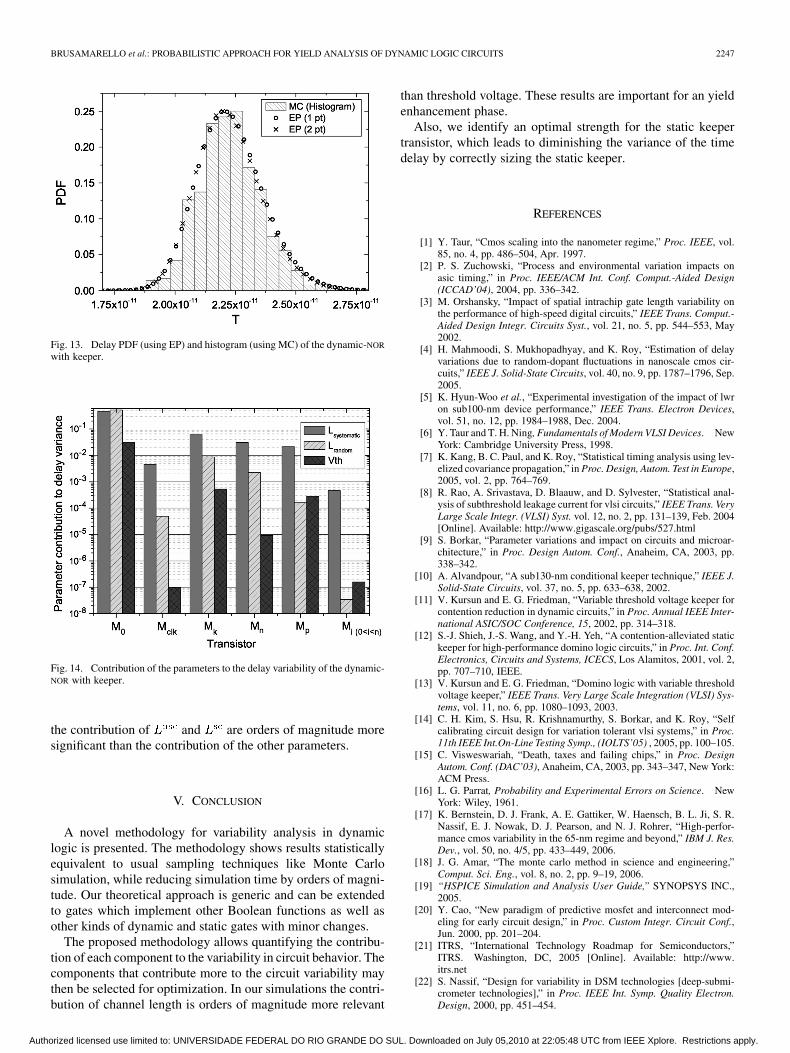
PDF of the gate delay is computed using (20), where canbe computed using EP and is approximated by the simulationusing nominal values. The Fig. 13 exposes the Gaussian PDF ofthe delay of the dynamic-NOR with static keeper. The plot devel-oped using the proposed methodology fits well to the histogramcomputed using MC. In order to draw the PDF using EP, we run19 simulations in the case of derivatives using 1 point aroundmean, and 36 electrical simulations when using 2 points. Thisrepresents an improvement in the running time up to 50 com-pared to MC using .
Fig. 14 presents the contribution of each parameter tothe delay variability. They were computed according to theSection II-D. As in the case of the dynamic-NOR without keeper,
Authorized licensed use limited to: UNIVERSIDADE FEDERAL DO RIO GRANDE DO SUL. Downloaded on July 05,2010 at 22:05:48 UTC from IEEE Xplore. Restrictions apply.
BRUSAMARELLO et al.: PROBABILISTIC APPROACH FOR YIELD ANALYSIS OF DYNAMIC LOGIC CIRCUITS 2247
Fig. 13. Delay PDF (using EP) and histogram (using MC) of the dynamic-NOR
with keeper.
Fig. 14. Contribution of the parameters to the delay variability of the dynamic-NOR with keeper.
the contribution of and are orders of magnitude moresignificant than the contribution of the other parameters.
V. CONCLUSION
A novel methodology for variability analysis in dynamiclogic is presented. The methodology shows results statisticallyequivalent to usual sampling techniques like Monte Carlosimulation, while reducing simulation time by orders of magni-tude. Our theoretical approach is generic and can be extendedto gates which implement other Boolean functions as well asother kinds of dynamic and static gates with minor changes.
The proposed methodology allows quantifying the contribu-tion of each component to the variability in circuit behavior. Thecomponents that contribute more to the circuit variability maythen be selected for optimization. In our simulations the contri-bution of channel length is orders of magnitude more relevant
than threshold voltage. These results are important for an yieldenhancement phase.
Also, we identify an optimal strength for the static keepertransistor, which leads to diminishing the variance of the timedelay by correctly sizing the static keeper.
REFERENCES
[1] Y. Taur, “Cmos scaling into the nanometer regime,” Proc. IEEE, vol.85, no. 4, pp. 486–504, Apr. 1997.
[2] P. S. Zuchowski, “Process and environmental variation impacts onasic timing,” in Proc. IEEE/ACM Int. Conf. Comput.-Aided Design(ICCAD’04), 2004, pp. 336–342.
[3] M. Orshansky, “Impact of spatial intrachip gate length variability onthe performance of high-speed digital circuits,” IEEE Trans. Comput.-Aided Design Integr. Circuits Syst., vol. 21, no. 5, pp. 544–553, May2002.
[4] H. Mahmoodi, S. Mukhopadhyay, and K. Roy, “Estimation of delayvariations due to random-dopant fluctuations in nanoscale cmos cir-cuits,” IEEE J. Solid-State Circuits, vol. 40, no. 9, pp. 1787–1796, Sep.2005.
[5] K. Hyun-Woo et al., “Experimental investigation of the impact of lwron sub100-nm device performance,” IEEE Trans. Electron Devices,vol. 51, no. 12, pp. 1984–1988, Dec. 2004.
[6] Y. Taur and T. H. Ning, Fundamentals of Modern VLSI Devices. NewYork: Cambridge University Press, 1998.
[7] K. Kang, B. C. Paul, and K. Roy, “Statistical timing analysis using lev-elized covariance propagation,” in Proc. Design, Autom. Test in Europe,2005, vol. 2, pp. 764–769.
[8] R. Rao, A. Srivastava, D. Blaauw, and D. Sylvester, “Statistical anal-ysis of subthreshold leakage current for vlsi circuits,” IEEE Trans. VeryLarge Scale Integr. (VLSI) Syst. vol. 12, no. 2, pp. 131–139, Feb. 2004[Online]. Available: http://www.gigascale.org/pubs/527.html
[9] S. Borkar, “Parameter variations and impact on circuits and microar-chitecture,” in Proc. Design Autom. Conf., Anaheim, CA, 2003, pp.338–342.
[10] A. Alvandpour, “A sub130-nm conditional keeper technique,” IEEE J.Solid-State Circuits, vol. 37, no. 5, pp. 633–638, 2002.
[11] V. Kursun and E. G. Friedman, “Variable threshold voltage keeper forcontention reduction in dynamic circuits,” in Proc. Annual IEEE Inter-national ASIC/SOC Conference, 15, 2002, pp. 314–318.
[12] S.-J. Shieh, J.-S. Wang, and Y.-H. Yeh, “A contention-alleviated statickeeper for high-performance domino logic circuits,” in Proc. Int. Conf.Electronics, Circuits and Systems, ICECS, Los Alamitos, 2001, vol. 2,pp. 707–710, IEEE.
[13] V. Kursun and E. G. Friedman, “Domino logic with variable thresholdvoltage keeper,” IEEE Trans. Very Large Scale Integration (VLSI) Sys-tems, vol. 11, no. 6, pp. 1080–1093, 2003.
[14] C. H. Kim, S. Hsu, R. Krishnamurthy, S. Borkar, and K. Roy, “Selfcalibrating circuit design for variation tolerant vlsi systems,” in Proc.11th IEEE Int.On-Line Testing Symp., (IOLTS’05) , 2005, pp. 100–105.
[15] C. Visweswariah, “Death, taxes and failing chips,” in Proc. DesignAutom. Conf. (DAC’03), Anaheim, CA, 2003, pp. 343–347, New York:ACM Press.
[16] L. G. Parrat, Probability and Experimental Errors on Science. NewYork: Wiley, 1961.
[17] K. Bernstein, D. J. Frank, A. E. Gattiker, W. Haensch, B. L. Ji, S. R.Nassif, E. J. Nowak, D. J. Pearson, and N. J. Rohrer, “High-perfor-mance cmos variability in the 65-nm regime and beyond,” IBM J. Res.Dev., vol. 50, no. 4/5, pp. 433–449, 2006.
[18] J. G. Amar, “The monte carlo method in science and engineering,”Comput. Sci. Eng., vol. 8, no. 2, pp. 9–19, 2006.
[19] “HSPICE Simulation and Analysis User Guide,” SYNOPSYS INC.,2005.
[20] Y. Cao, “New paradigm of predictive mosfet and interconnect mod-eling for early circuit design,” in Proc. Custom Integr. Circuit Conf.,Jun. 2000, pp. 201–204.
[21] ITRS, “International Technology Roadmap for Semiconductors,”ITRS. Washington, DC, 2005 [Online]. Available: http://www.itrs.net
[22] S. Nassif, “Design for variability in DSM technologies [deep-submi-crometer technologies],” in Proc. IEEE Int. Symp. Quality Electron.Design, 2000, pp. 451–454.
Authorized licensed use limited to: UNIVERSIDADE FEDERAL DO RIO GRANDE DO SUL. Downloaded on July 05,2010 at 22:05:48 UTC from IEEE Xplore. Restrictions apply.

2248 IEEE TRANSACTIONS ON CIRCUITS AND SYSTEMS—I: REGULAR PAPERS, VOL. 55, NO. 8, SEPTEMBER 2008
Lucas Brusamarello (S’07) was born in Caxias doSul, Brazil. He received the B.S. and M.Sc. degreesin computer science from the Federal University ofRio Grande do Sul (UFRGS), Porto Alegre, Brazil,in 2005 and 2007, respectively.
From 2001 to 2005, he worked with the Micro-electronics Group at UFRGS (GME-UFRGS), devel-oping stochastic algorithms and parallel algorithmsfor physical synthesis problems. In 2005 and 2006,as a Researcher in Post-Graduate Program on Com-puting (PPGC), he worked on yield analysis. From
2006 to 2008, he worked in the Computer-Aided Design Division, Fujitsu Lab-oratories of America, Inc., Sunnyvale, CA. His research interests include yieldanalysis, design for yield, statistical modeling, numerical methods, physical syn-thesis, clock synthesis and stochastic algorithms.
Roberto da Silva was born in Mauá, São Paulo,Brazil, on December 16, 1973. He received the B.S.and Ph.D degrees in physics from the University ofSão Paulo (USP) in 1998 and 2002, respectively.
From 1998 to 2002, he worked on statistical me-chanics, mathematical physics, and computationalphysics where most of his papers are publishedin indexed journals and more recently in confer-ences qualified as Qualis A (according to Brazilianresearch agency—CAPES). Since 2003, he is Pro-fessor at the Federal University of Rio Grande do
Sul, Porto Alegre, Brazil. His research interests include, Numerical, analyticaland statistical modeling of the systems physically and biologically motivated,computing and probability: applications in information retrieval, graph theory.game theory and dynamical systems: analytical and computational aspects.
Gilson I. Wirth (M’97–SM’07) received theB.S.E.E. and M.Sc. degrees from the UniversidadeFederal do Rio Grande do Sul, Brazil, in 1990 and1994, respectively, and the Dr.-Ing. degree in elec-trical engineering from the University of Dortmund,Dortmund, Germany, in 1999.
From 2000 to 2002, he worked as Lecturer and Re-searcher in the field of microelectronics at the Infor-matics Institute, Universidade Federal do Rio Grandedo Sul. From July 2002 to December 2006 he waswith the Computer Engineering Department, Univer-
sidade Estadual do Rio Grande do Sul (UERGS), where he was a Professor andhead of the research group in micro- and nano-electronics. In January 2007 hejoined the Electrical Engineering Department at the Universidade Federal doRio Grande do Sul (UFRGS), as a professor. In July, August and December2001 he was at Motorola, Austin, Texas, working in CMOS process technologytransfer to CEITEC, Porto Alegre, Brazil. In February and March 2002 he wasat the Corporate Research Department of Infineon Technologies, Munich, Ger-many, working as guest researcher on low-frequency noise in deep-submicrom-eter MOS devices. His research interests include low-frequency noise, radiationeffects, variability and design for yield of digital, analog and mixed-signal cir-cuits.
Ricardo A. L. Reis (M’81–SM’06) was born inCruz Alta, Brazil. He received the B.S. degree inelectrical engineering from the Federal University ofRio Grande do Sul (UFRGS), Porto Alegre, Brazil,in 1978, and the Ph.D. degree in microelectronicsfrom the National Polytechnic Institute, Grenoble,France, in 1983.
Since 1981, he has been a Professor with theInformatics Institute, UFRGS. His research interestsinclude physical design automation, microelec-tronics education, and fault-tolerant microelectronic
systems.Dr. Reis was Vice-President of International Federation for Information Pro-
cessing (IFIP) and he was also President of the Brazilian Microlectronics So-ciety and Vice-President of the Brazilian Microelectronics Society. He is oneof the founders of the SBCCI [the major conference sponsored by IEEE Cir-cuits and Systems (CAS) Society in South America]. He was also the GeneralChair of several conferences like IEEE ISVLSI, SBCCI, IFIP VLSI-SoC. He isalso active in the organization of several others international conferences. Prof.Reis is the Chair of the Steering Committee of the IFIP/CEDA VLSI-SoC se-ries of conferences and vice-chair of the IFIP WG10.5. He is the founder of theRio Grande do Sul IEEE CAS Chapter. In 2002 he received an award as theresearcher of the year of the state of Rio Grande do Sul, Brazil. He received theSilver Core Award from IFIP.
Authorized licensed use limited to: UNIVERSIDADE FEDERAL DO RIO GRANDE DO SUL. Downloaded on July 05,2010 at 22:05:48 UTC from IEEE Xplore. Restrictions apply.