2240 fiber optic modem user manual - canoga...
TRANSCRIPT
2240 Fiber Optic Modem
User Manual

NOTICE
Canoga Perkins has prepared this user’s manual for use by customers and Canoga Perkins personnel as a guide for the proper installation, operation and/or
maintenance of Canoga Perkins equipment. The drawings, specifications and information contained in this document are the property of Canoga Perkins and any unauthorized use or disclosure of such drawings, specifications and information is
prohibited.
Canoga Perkins reserves the right to change or update the contents of this manual and to change the specifications of its products at any time without prior notification. Every
effort has been made to keep the information in this document current and accurate as of the date of publication or revision. However, no guarantee is given or implied that the
document is error free or that it is accurate with regard to any specification.
CANOGA PERKINS CORPORATION20600 Prairie Street
Chatsworth, California 91311-6008Business Phone: (818) 718-6300
(Monday through Friday 7 a.m. - 5 p.m. Pacific Time) FAX: (818) 718-6312 (24 hrs.)
Website: www.canoga.comE-mail: [email protected]
Copyright © 1991-2011 Canoga Perkins CorporationAll Rights Reserved
2240 Fiber Optic Modem User ManualProduct Number 6911100
Revision S 05/2011
Canoga Perkins is a registered trademarks of Canoga Perkins Corp.To find Technical Advisories and Product Release Notes, visit to the Canoga Perkins
website at http://www.canoga.com.

2240 Fiber Optic Modem User Manual
CAUTION!This product may contain a laser diode emitter operating at a wavelength of 1300 nm - 1600 nm. Use of optical instruments (for example: collimating optics) with this product may increase eye hazard. Use of controls or adjustments or performing procedures other than those specified herein may result in hazardous radiation exposure.
Under normal conditions, the radiation levels emitted by this product are under the Class 1 limits in 21 CFR Chapter 1, Subchapter J.
ATTENTION!Ce produit peut contenir un émetteur de diode de laser fonctionnant à une longueur d'onde 1300 de nm - nm 1600. Utilisation des instruments optiques (par exemple: la collimation du système optique) avec ce produit peut augmenter le danger. L'utilisation des commandes ou des ajustements ou les procédures d'exécution autre que ceux indiquées ci-dessus peut avoir comme conséquence l'exposition de la radiation dangereuse.
Dans des conditions normales, les niveaux de rayonnement émis par ce produit sont sous les limites de la classe 1 en chapitre 1, Subchapter J de 21 CFR.
NOTICE!This device contains static sensitive components. It should be handled only with proper Electrostatic Discharge (ESD) grounding procedures.
AVIS!Ce dispositif contient les composants sensibles statiques. Il devrait être manipulé seulement avec la Décharge Electrostatique (DES) appropriée procédures.
3

General Safety ConsiderationsInstallation
The 2240 is suitable for installation in network telecommunication facilities and locations where the National Electric Code (NEC) applies.
Cabling
This equipment does not have direct electrical connection to outside plant equipment.
The copper ports of the 2240 are not intended for direct connection to “outside plant” metallic conductors and shall be isolated (by channel banks or office repeaters) from any connections to network or terminal equipment that lie outside of the same building. The telecommunication interface connections are considered to be, and meet the requirements of, SELV circuits (not TNV).
Power
WARNING: The 2240 installed in a 2201 Chassis with redundant power supplies must have both power supply cords disconnected before servicing.
Wiring methods used for the connection of the equipment to the AC or DC MAINS SUPPLY shall be in accordance with the National Electrical Code, ANSI/NFPA 70, and the Canadian Electrical Code, Part I, CSA C22.1.
The 2240 Stand Alone units do not incorporate a disconnect device. The plug on the power supply cord is intended to serve as the disconnect device. It is also recommended that the AC socket-outlet shall be installed near the equipment and shall be easily accessible.
Fuses
The 2240 stand alone is not equipped with internal fuses. The 2201 Chassis is fused at 2A Slow Blow.
Although not required, an external fuse may be used to isolate the unit in a shared fuse distribution panel. In that case, the unit should be fused with a 3A slow blow fuse or a 5A fast acting fuse.
Surge Protection
The 2240 does not contain an internal Surge Protective Device (SPD). An external SPD should be used at the AC input of the network equipment according to facilities procedures and as defined by the NEC.
4
2240 Fiber Optic Modem User Manual
Grounding
The 2240 is suitable for installation as part of the Common Bonding Network (CBN). The 2240 is provided with a safety ground connection which is capable of conducting any fault current likely to be imposed, such as fault current from sources within the chassis. The unit will be grounded using the ground conductor of the power cord and must be connected to an earthed mains socket-outlet.
An electrical conducting path should exist between the 2240 chassis and the metal surface of the enclosure or rack in which it is mounted or to a grounding conductor. Electrical continuity should be provided by using thread-forming type mounting screws that remove any paint or non-conductive coatings and establish a metal-to-metal contact. Any paint or other nonconductive coatings should be removed on the surfaces between the mounting hardware and the enclosure or rack. The surfaces should be cleaned and an antioxidant applied before installation.
Lightning Protection
The intra-building ports of the 2240 are suitable for connection to intra-building or unexposed wiring or cabling only. The intra-building ports of the equipment or subassembly MUST NOT be metallically connected to interfaces that connect to the OSP or its wiring. These interfaces are designed for use as intra-building interfaces only (Type 2 or Type 4 ports as described in GR-1089-CORE, Issue 4) and require isolation from the exposed OSP cabling. The addition of Primary Protectors is not sufficient protection in order to connect these interfaces metallically to OSP wiring.
To protect the port against intra-building lightning surges, the ports of the 2240 are suitable for connection to shielded intra-building cabling grounded at both ends.
ESD
The 2240 has been tested and passes the ESD requirements of test level 4 for air and contact discharges. Protecting the exposed components from electrostatic damage when removing or replacing the modules requires the proper use of static mitigation procedures such asproperly wearing a wrist strap.
Operation Temperature
The 2240 is designed and Nationally Recognized Test Laboratory (NRTL) tested and verified to operate between 0°C to 50°C, and type tested for short term emergency ambient temperature of -5°C to 55°C.
Emissions and Immunity
This device complies with part 15 of the FCC rules. Operation is subject to the following two conditions:
1. This device may not cause harmful interference
5

2. This device must accept any interference received, including interference that may cause undesired operation.
The authority to operate this equipment is conditioned by the requirements that no modifications will be made to the equipment unless the changes or modifications are expressly approved by the Canoga Perkins Corporation.
To Users of Digital Apparatus in Canada: This Class A digital apparatus meets all requirements of the Canadian interference-causing equipment regulations.
Aux utilisateurs des appareils numérique au Canada: Cet appareil numérique de la classe A respecte toutes les exigences du règlement sur le matérial brouilleur du Canada.
Special Accessories
The 2240 does not require any special accessories to achieve compliance for emission and immunity criteria.
Double Pole/Neutral Fusing
On the 2240 a fuse may be in place in the neutral path on the AC power supply. After operation of the fuse, parts of the equipment that remain energized might represent a hazard during servicing.
Waste Electrical and Electronic Equipment (WEEE)
Product Disposal Information
Do not dispose of this product in unsorted municipal waste. This product is recyclable, and should be recycled according to your local standards. For more information, contact Canoga Perkins technical support.
6
2240 Fiber Optic Modem User Manual
7
Chapter 1. Introduction ........................................................................ 13
1.1. 2240 Modem .................................................................................................. 13
1.1.1. LEDs and Switches .............................................................................................. 14
1.2. 2201 Rack Chassis ........................................................................................ 15
1.3. 2202 Modem Shelf ......................................................................................... 16
1.4. 2200R Series Redundant Card ...................................................................... 16
1.5. Modem Operation........................................................................................... 16
1.5.1. General ................................................................................................................ 16
1.5.2. System Test and Diagnostics............................................................................... 18
1.5.3. Transmit Section .................................................................................................. 18
1.5.4. Receive Section ................................................................................................... 18
1.5.5. Expanded Interface Control Channels ................................................................. 19
1.5.6. Expanded Interface Auxiliary Channels ............................................................... 19
1.5.7. Fiber Optics.......................................................................................................... 19
1.6. Loss Budget ................................................................................................... 19
1.7. Initial Unit Testing........................................................................................... 19
Chapter 2. Installation and Setup ........................................................ 21
2.1. Setup .............................................................................................................. 21
2.1.1. Unpacking the Unit............................................................................................... 21
2.1.2. HI/LO Optic Power Switch.................................................................................... 21
2.1.3. Internal Control Switches ..................................................................................... 22
2.1.3.1. Carrier Detect (CD) Signal Options ................................................. 23
2.1.3.2. Internal Clock Option Switches........................................................ 24
2.1.3.3. TBL/NORM Switch........................................................................... 24
Contents
2240 Fiber Optic Modem User Manual
8
2.1.3.4. CLK/EXT Switch .............................................................................. 24
2.1.4. Signal Ground Strap............................................................................................. 24
2.1.5. SCT Normal/Invert Jumper .................................................................................. 24
2.1.6. EXTRA CLOCK Jumper....................................................................................... 25
2.1.7. Setting Up a Tail Circuit ....................................................................................... 26
2.2. Installation ...................................................................................................... 27
2.2.1. Standalone Modem Installation............................................................................ 27
2.2.2. Rack-Mount Modem Installation........................................................................... 28
2.2.3. Fiber Cable and Connectors ................................................................................ 28
2.2.4. 2202 Modem Shelf Installation............................................................................. 28
2.2.5. Custom Oscillator Installation............................................................................... 29
Chapter 3. Mode and Rate Selection................................................... 31
3.1. Operating Mode, Data Rate Selection............................................................ 31
3.2. External Clock Modes .................................................................................... 33
3.2.1. Sampled External Clock Mode - Mode 0.............................................................. 33
3.2.2. Locked External Clock Mode - Mode 7 ................................................................ 34
3.3. Internal Clock Modes - Modes 1, 2, 3, 4......................................................... 34
3.3.1. Standard Internal Clock Rates (Groups 1, 2 and 3) ............................................. 35
3.3.2. Custom Internal Clock Rates (Group 4) ............................................................... 35
3.4. Slave Clock Mode - Mode 5 ........................................................................... 37
3.4.1. Loopback Clock for Slave Mode .......................................................................... 37
3.5. Asynchronous Mode - Mode 6 ....................................................................... 37
3.6. Consideration of Propagation Delays............................................................. 38
3.7. Internal Clock Option Switches ...................................................................... 39
3.7.1. TBL/NORM Switch ............................................................................................... 39
3.7.2. CLK/EXT Switch................................................................................................... 39
Chapter 4. Data Interfaces.................................................................... 41
2240 Fiber Optic Modem User Manual
9
4.1. Data Interfaces Overview............................................................................... 41
4.2. RS-423/232D Model 432................................................................................ 42
4.2.1. DCD Jumper ........................................................................................................ 43
4.2.2. CTS_GATE Jumper ............................................................................................. 44
4.2.3. DSR Jumper......................................................................................................... 44
4.2.4. CH_GND Jumper ................................................................................................. 44
4.3. RS-449/422 Model 422 .................................................................................. 44
4.3.1. RS_BIAS Jumper ................................................................................................. 46
4.3.2. RR Jumper ........................................................................................................... 46
4.3.3. CS_GATE Jumper ............................................................................................... 47
4.3.4. DM Jumper........................................................................................................... 47
4.3.5. CH_GND Jumper ................................................................................................. 47
4.3.6. UNBAL_REF Jumper ........................................................................................... 47
4.4. RS-530 Interface Model 430 .......................................................................... 47
4.4.1. RTS_BIAS Jumper............................................................................................... 49
4.4.2. DCD Jumper ........................................................................................................ 49
4.4.3. DSR Jumper......................................................................................................... 49
4.4.4. CHASSIS_GND Jumper ...................................................................................... 49
4.4.5. SCT Switch .......................................................................................................... 49
4.4.6. CTS_GATE Jumper ............................................................................................. 50
4.4.7. CTS_OUT Jumper ............................................................................................... 50
4.4.8. CTS (A) Jumper ................................................................................................... 50
4.4.9. 1 KG_SWING Jumper.......................................................................................... 50
4.4.10. 2 KG_OUT Jumper ............................................................................................ 50
4.5. CCITT V.35 (ISO 2593-1993) Model 436....................................................... 51
4.5.1. RTS_BIAS Jumper............................................................................................... 53
4.5.2. DCD Jumper ........................................................................................................ 53
4.5.3. CTS_GATE Jumper ............................................................................................. 54
4.5.4. DSR Jumper......................................................................................................... 54
2240 Fiber Optic Modem User Manual
10
4.5.5. CH_GND Jumper ................................................................................................. 54
4.6. Multi-Channel Interfaces ................................................................................ 54
4.6.1. RS-449/RS-423 Model MC1 ................................................................................ 54
4.6.2. RS-449/422 Interface ........................................................................................... 55
4.6.3. RS_BIAS Jumper ................................................................................................. 57
4.6.4. RR Jumper ........................................................................................................... 57
4.6.5. CS_GATE Jumper ............................................................................................... 57
4.6.6. CH_GND Jumper ................................................................................................. 57
4.6.7. UNBAL_REF Jumper ........................................................................................... 57
4.6.8. RS-423/DB-25 Interface....................................................................................... 58
4.6.9. V.35/RS-423 Model MC2 ..................................................................................... 59
4.6.10. CCITT V.35/MRC 34 Interface ........................................................................... 60
4.6.11. RTS_BIAS Jumper............................................................................................. 62
4.6.12. DCD Jumper ...................................................................................................... 62
4.6.13. CTS_GATE Jumper ........................................................................................... 62
4.6.14. CH_GND Jumper ............................................................................................... 62
4.6.15. RS-423/DB-25 Interface..................................................................................... 62
4.7. T1/E1 Interfaces ............................................................................................. 63
4.7.1. Transparent Bipolar - Models 4BX....................................................................... 63
4.8. TTL/BNC Interface Model -BN ....................................................................... 66
4.9. Programmable Buffered Interface/Model P53 ................................................ 67
4.9.1. Jumper and Switch Settings................................................................................. 71
4.9.2. Generic Interface.................................................................................................. 72
4.9.3. External Station.................................................................................................... 74
4.9.4. Internal ................................................................................................................. 75
4.9.5. External ................................................................................................................ 76
4.9.6. DTE Adapter ........................................................................................................ 77
4.9.7. Legacy Adapter .................................................................................................... 78
4.10. High-Speed RS-422/Mil-Std 188-114C Interfaces ....................................... 79
2240 Fiber Optic Modem User Manual
11
4.10.1. Model TW........................................................................................................... 79
4.10.2. Model TW8......................................................................................................... 80
4.10.3. Model T22 .......................................................................................................... 81
4.10.4. Model T88 .......................................................................................................... 81
4.10.5. Model D22.......................................................................................................... 81
4.10.6. Model D88.......................................................................................................... 81
4.11. Interface Reconfiguration ............................................................................. 83
4.12. Standalone Reconfiguration ......................................................................... 84
Chapter 5. Troubleshooting ................................................................. 85
5.1. Diagnostic Procedures ................................................................................... 85
5.2. Local and Remote Loopback.......................................................................... 85
5.2.1. Loopback Tests.................................................................................................... 85
5.2.2. Remote Loopback Test ........................................................................................ 86
Chapter 6. Diagnostic Procedures ...................................................... 87
6.1. 2240/2201 Diagnostic Procedures ................................................................. 87
6.1.1. Required Equipment ............................................................................................ 87
6.2. Loopback Test Diagnostic Procedure ............................................................ 88
6.3. Fiber Optic Diagnostic Procedure .................................................................. 89
Chapter 7. Specifications ..................................................................... 91
7.1. Optical Interface ............................................................................................. 91
7.1.1. Distance Guide..................................................................................................... 93
7.2. System Electrical............................................................................................ 93
7.3. Indicators and Controls .................................................................................. 94
7.4. Physical and Environmental ........................................................................... 94
7.5. 2240 Fiber Optic Modem Configurations........................................................ 95

13
Chapter 1
Introduction
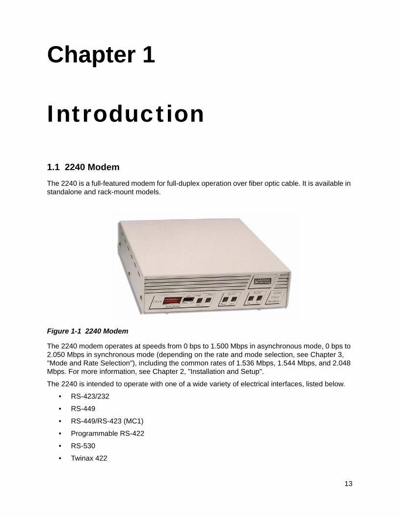
1.1 2240 ModemThe 2240 is a full-featured modem for full-duplex operation over fiber optic cable. It is available in standalone and rack-mount models.
Figure 1-1 2240 Modem
The 2240 modem operates at speeds from 0 bps to 1.500 Mbps in asynchronous mode, 0 bps to 2.050 Mbps in synchronous mode (depending on the rate and mode selection, see Chapter 3, "Mode and Rate Selection"), including the common rates of 1.536 Mbps, 1.544 Mbps, and 2.048 Mbps. For more information, see Chapter 2, "Installation and Setup".
The 2240 is intended to operate with one of a wide variety of electrical interfaces, listed below.
• RS-423/232
• RS-449
• RS-449/RS-423 (MC1)
• Programmable RS-422
• RS-530
• Twinax 422
Chapter 1 Introduction 2240 Fiber Optic Modem User Manual2240 Modem
14
• Twinaxial Mil-Std 188-114C
• DC-37 Mil-Std 188-114
• CCITT V.35
• Transparent T1/E1
• CCITT V.35/RS-423 (MC2)
• TTL/BNC
Various configurations of the 2240 provide local and end-to-end modem controls, including those listed below.
Data/Clock:
• Send Data
• Receive Data
• Send Timing
• Receive Timing
• Terminal Timing
Controls:
• Request to Send
• Clear To Send
• Data Set Ready
• Data Carrier Detect
• Local Test
• Remote Test
• Sec. Request to Send
• Sec. Data Carrier Detect
• Data Terminal Ready
• Ring Indicator
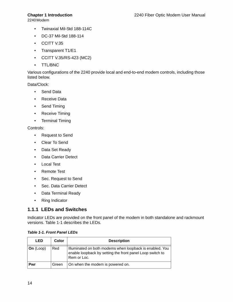
1.1.1 LEDs and SwitchesIndicator LEDs are provided on the front panel of the modem in both standalone and rackmount versions. Table 1-1 describes the LEDs.
Table 1-1. Front Panel LEDs
LED Color Description
On (Loop) Red Illuminated on both modems when loopback is enabled. You enable loopback by setting the front panel Loop switch to Rem or Loc.
Pwr Green On when the modem is powered on.
Chapter 1 Introduction2201 Rack Chassis
15
An 8-position DIP switch labeled Clock is on the front panel. This switch is for control of operating modes and internal clock rates. For more information, see Chapter 3, "Mode and Rate Selection".
A loopback control switch labeled Loop is located on the front panel. Use of this switch is covered in Chapter 5, "Troubleshooting", and Chapter 6, "Diagnostic Procedures".
The electrical power connection and fiber optic connections are made on the rear panel of the modem.
The HI/LO optical power switch is also located the rear panel of the modem. For more information, see “HI/LO Optic Power Switch” on page 21.
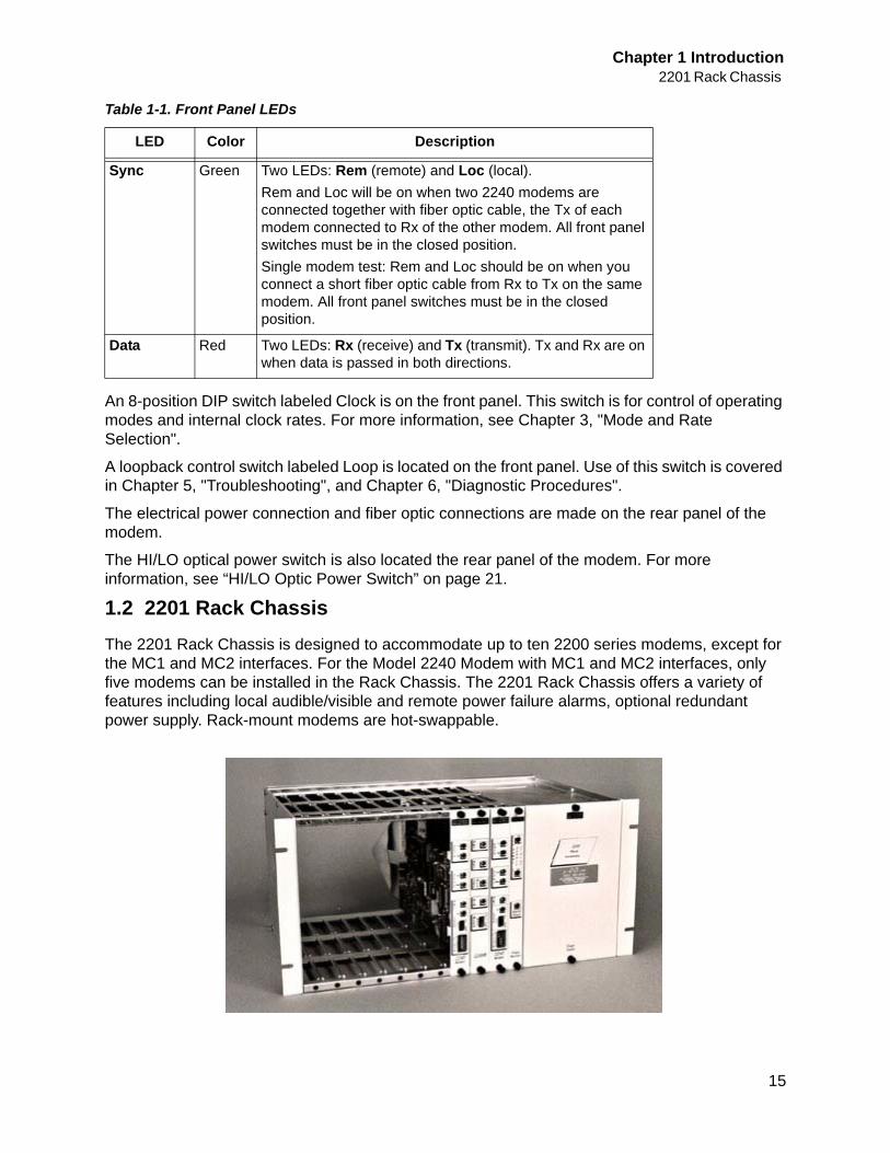
1.2 2201 Rack ChassisThe 2201 Rack Chassis is designed to accommodate up to ten 2200 series modems, except for the MC1 and MC2 interfaces. For the Model 2240 Modem with MC1 and MC2 interfaces, only five modems can be installed in the Rack Chassis. The 2201 Rack Chassis offers a variety of features including local audible/visible and remote power failure alarms, optional redundant power supply. Rack-mount modems are hot-swappable.
Sync Green Two LEDs: Rem (remote) and Loc (local).Rem and Loc will be on when two 2240 modems are connected together with fiber optic cable, the Tx of each modem connected to Rx of the other modem. All front panel switches must be in the closed position.Single modem test: Rem and Loc should be on when you connect a short fiber optic cable from Rx to Tx on the same modem. All front panel switches must be in the closed position.
Data Red Two LEDs: Rx (receive) and Tx (transmit). Tx and Rx are on when data is passed in both directions.
Table 1-1. Front Panel LEDs
LED Color Description
Chapter 1 Introduction 2240 Fiber Optic Modem User Manual2202 Modem Shelf
16
Figure 1-2 2201 Rack Chassis
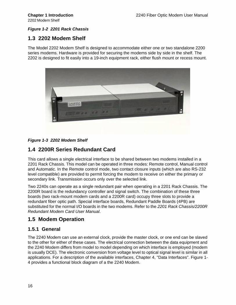
1.3 2202 Modem ShelfThe Model 2202 Modem Shelf is designed to accommodate either one or two standalone 2200 series modems. Hardware is provided for securing the modems side by side in the shelf. The 2202 is designed to fit easily into a 19-inch equipment rack, either flush mount or recess mount.
Figure 1-3 2202 Modem Shelf
1.4 2200R Series Redundant CardThis card allows a single electrical interface to be shared between two modems installed in a 2201 Rack Chassis. This model can be operated in three modes: Remote control, Manual control and Automatic. In the Remote control mode, two contact closure inputs (which are also RS-232 level compatible) are provided to permit forcing the modem to receive on either the primary or secondary link. Transmission occurs only over the selected link.
Two 2240s can operate as a single redundant pair when operating in a 2201 Rack Chassis. The 2200R board is the redundancy controller and signal switch. The combination of these three boards (two rack-mount modem cards and a 2200R card) occupy three slots to provide a redundant fiber optic path. Special interface boards, Redundant Paddle Boards (4PB) are substituted for the normal I/O boards in the two modems. Refer to the 2201 Rack Chassis/2200R Redundant Modem Card User Manual.
1.5 Modem Operation
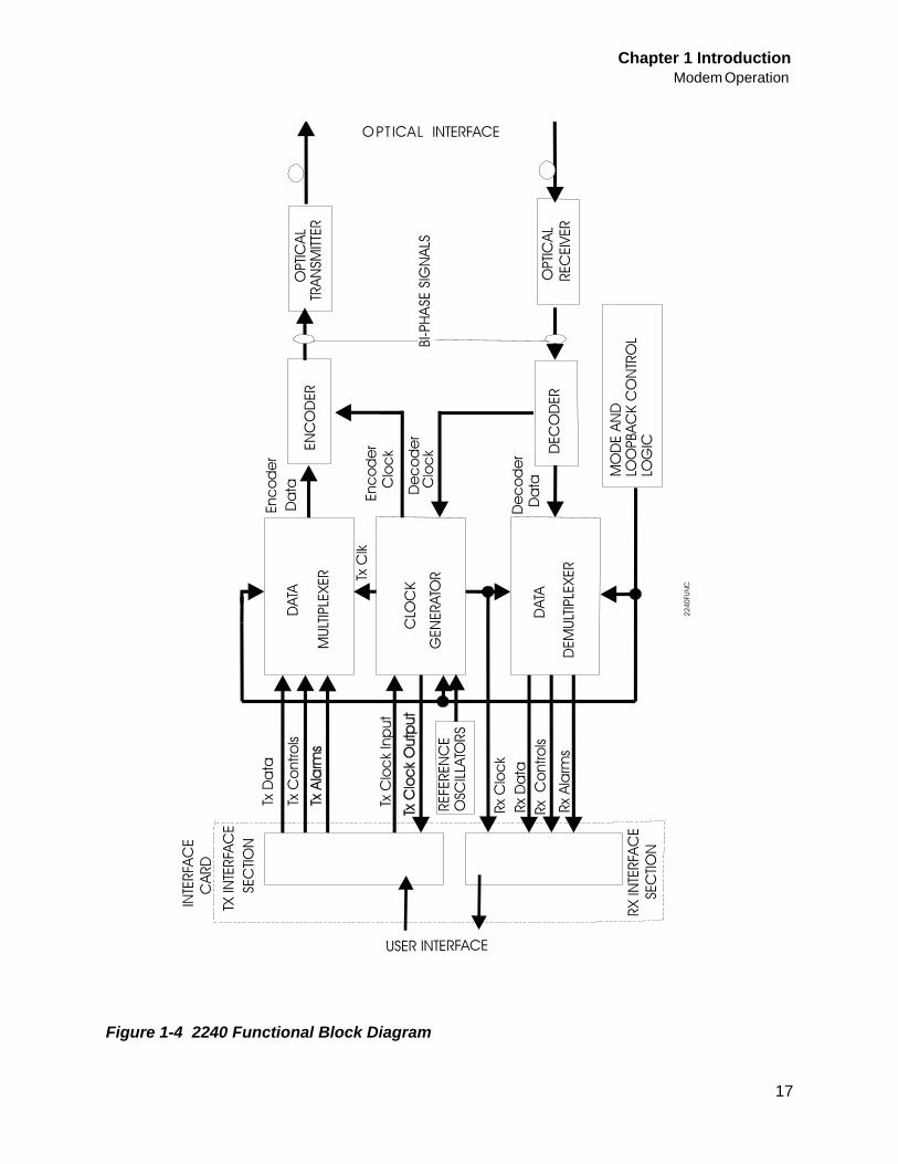
1.5.1 GeneralThe 2240 Modem can use an external clock, provide the master clock, or one end can be slaved to the other for either of these cases. The electrical connection between the data equipment and the 2240 Modem differs from model to model depending on which interface is employed (modem is usually DCE). The electronic conversion from voltage level to optical signal level is similar in all applications. For a description of the available interfaces, Chapter 4, "Data Interfaces". Figure 1-4 provides a functional block diagram of a the 2240 Modem.
Chapter 1 IntroductionModem Operation
17
Figure 1-4 2240 Functional Block Diagram
Chapter 1 Introduction 2240 Fiber Optic Modem User ManualModem Operation
18
The modem functions as a 10-channel multiplexer. The following discussion assumes an 8.19 MHz composite. Lower composite speeds result in proportionally lower submultiples. Clock and data are carried on a 4.096 Mbps and 2.048 Mbps channel, respectively. Each of the three control leads and five Auxiliary lines are carried on a 64 Kbps channel. The remaining 1.536 kbps bandwidth splits into 1.024 Mbps for multiplexer synchronization, 256 kbps for low-speed channel synchronization and
256 kbps for supervisory channels. Each 64 kbps channel can be used to carry an async data signal if the user's equipment can tolerate the 16 microseconds of pulse distortion due to sampling.
The composite speed of the 2240 Modem varies between 4.1 and 8.2 Mbps, depending on the selected mode of operation. A detailed description of mode selection is in Chapter 3, "Mode and Rate Selection". A brief description follows.
The modem has two basic external clock operating modes: Sampled and External Locked. In the Sampled mode, the composite speed is fixed at 8.192 MHz and clock, data and control/auxiliary channels are sampled at 4.096, 2.048 and .064 MHz, respectively. This mode is recommended for low data speed applications (less than 128 kbps).
For the External Locked modes, the composite speed is a multiple of an external clock. For T1 and E1, the multiple is four and the resulting composite rates are 6.176 and 8.192 MHz, respectively. Also, for the External Locked modes, the sampling frequency for the control and auxiliary channels is 1/128th of the composite rate. Therefore, this sampling rate can vary from 32 to 64 kHz, resulting in sampling jitter of 32 to 16 msec, respectively.
1.5.2 System Test and DiagnosticsBoth Local and Remote test modes can be invoked via a front panel switch. These are useful for diagnosing system problems. See Chapter 5, "Troubleshooting" and Chapter 6, "Diagnostic Procedures" for more details on these test modes. Two front panel LEDs, Loc and Rem Sync, also help to isolate system problems by indicating whether the local and remote composites are synchronized.
1.5.3 Transmit SectionEach interface signal input to the modem is converted to logic level for use by the modem circuit. The logic level signal is then multiplexed and encoded into a bi-phase data stream, which in turn is converted to an optical signal for transmission over the fiber optic cable.
The heart of the 2240 transmitter is a ten-channel multiplexer. This multiplexer takes the clock, data and control lead inputs from the interface, multiplexes them, then adds framing and supervisory information. This composite data is then converted into a Manchester-coded signal which drives the modulator of the optical transmitter.
The function of the multiplexer is highly dependent on the operating mode of the modem (see Chapter 3, "Mode and Rate Selection"). Supervisory information is related to frame synchronization and loopback status.
1.5.4 Receive SectionAn optical receiver circuit converts the incoming signal to a biphase logic signal. It is then de-multiplexed into all necessary interface signals.
Chapter 1 IntroductionLoss Budget
19
The receiver first extracts the clock and data information from the Manchester-coded optical signal. After frame-bit lock is established, the de-multiplexer separates out the clock, data and control lead signals, as well as the supervisory information. The supervisory states are mainly routed to control status indicators, while the remaining signals are routed to the interface circuits. The operation of the receiver is somewhat dependent on the 2240 operating mode, but much less dependent than the transmitter.
1.5.5 Expanded Interface Control ChannelsThe 400 series of 2200 Series Fiber Optic Modem Interfaces can support additional Control Leads up to a maximum of four. There are three channels dedicated to use for Control. For descriptions of these interfaces, see Chapter 4, "Data Interfaces". The fourth is the Aux Channel 1 input and output which is available on the expanded interface connector.
1.5.6 Expanded Interface Auxiliary ChannelsThe 2240 has five Auxiliary Channels. One of these channels is available on the expanded interface connector and the other four on the Auxiliary Interface Connector (see Figure 3-4). The MC1 and MC2 interfaces make use of all eight control and auxiliary channels (see Chapter 4, "Data Interfaces").
1.5.7 Fiber OpticsEach interface signal input to the modem is converted to logic level for use by the modem circuit. The logic level signal is then multiplexed and encoded into a biphase data stream, which in turn is converted to optical signal level for transmission over the fiber optic cable.
1.6 Loss BudgetThe maximum possible transmission distance is dependent on the overall power loss over the fiber optic link. This is called the link loss. The modem’s loss budget is determined by comparing the launch power at the modem with receiver sensitivity at the other end of the link. The difference is the loss budget.
For reliable operation over a long term, such as several years, the link loss should be at least 3 dB less than the modem's loss budget. This allows for minor increases in link loss through terminations and any slight deterioration in optical power output.
The connectors are clearly marked as to their function, either Transmit (Tx) or Receive (Rx), on the back panel of the 2240 standalone units, and on the rear of the 2201 Rack Chassis.
The 2240 modem can be used with most popular sizes of multimode and single mode optic cable, including 50/125, 62.5/125 and 8-10/125.
NOTE: When using 85/125 or 100/140 micron fiber optic cable, an inline attenuator may need to be installed between the 2240 and the Receive (Rx) fiber optic cable for proper modem operation.
1.7 Initial Unit TestingThe Remote and Local Sync indicators on the front panel constantly indicate link integrity. The Local Sync indicator blinks off momentarily if an error has been detected. The Loopback Test feature can be used to verify that the fiber optic modem link and electrical interface are installed correctly.

Chapter 1 Introduction 2240 Fiber Optic Modem User ManualInitial Unit Testing
20
21
Chapter 2
Installation and Setup
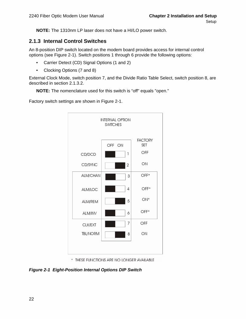
2.1 SetupThe setting up of the 2240 Modem includes the two-section HI/LO optic power switch, internal control switches and the signal ground strap. The setup, as described in the following sections, provides the initial configurations for operation of the unit.
2.1.1 Unpacking the UnitEach 2240 Modem is shipped factory tested, and packed in protective cartons. Unpack the unit and retain the shipping carton and protective packing for reuse in the event a need arises for returning it to the factory.
To assure proper operation of the modem, please inspect it and its shipping carton carefully for damage. If damage is sustained to the unit, file a liability claim immediately with the freight carrier.
2.1.2 HI/LO Optic Power SwitchAll versions, except for ELED and LP laser models, incorporate an optic power level dual DIP switch for varying the transmit power of the fiber optic LED or laser (see Figure 2-6). Both sections of the switch must be set the same. The switch for the 2240 standalone is located on the rear panel of its enclosure. (The switch for the 2240 Rack Chassis is located at the rear of the PC card, adjacent to the transmit optical connector.)
The optical power switch provides two settings for optical transmission level. The appropriate switch setting depends on the loss of the fiber optic link. Each optical model has a different transition point in terms of loss. Refer to Table 2-1 for the link loss ranges for each optical model.
For example, if the 850nm model is used and the link loss is 5 dB, use the LO setting on that line.
Table 2-1. Link Loss Range
ModelLink Loss Range
HI Power LO Power
850nm Standard >6 dB to Max <6 dB
1310nm HP laser >6 dB to Max <6 dB
2240 Fiber Optic Modem User Manual Chapter 2 Installation and SetupSetup
22
NOTE: The 1310nm LP laser does not have a HI/LO power switch.
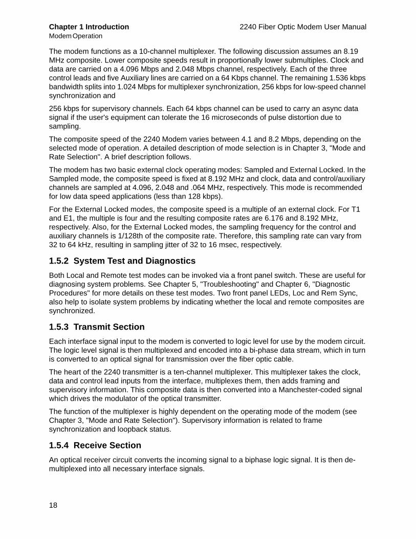
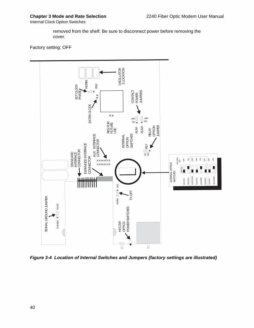
2.1.3 Internal Control SwitchesAn 8-position DIP switch located on the modem board provides access for internal control options (see Figure 2-1). Switch positions 1 through 6 provide the following options:
• Carrier Detect (CD) Signal Options (1 and 2)
• Clocking Options (7 and 8)
External Clock Mode, switch position 7, and the Divide Ratio Table Select, switch position 8, are described in section 2.1.3.2.
NOTE: The nomenclature used for this switch is “off" equals "open."
Factory switch settings are shown in Figure 2-1.
Figure 2-1 Eight-Position Internal Options DIP Switch
Chapter 2 Installation and SetupSetup
23
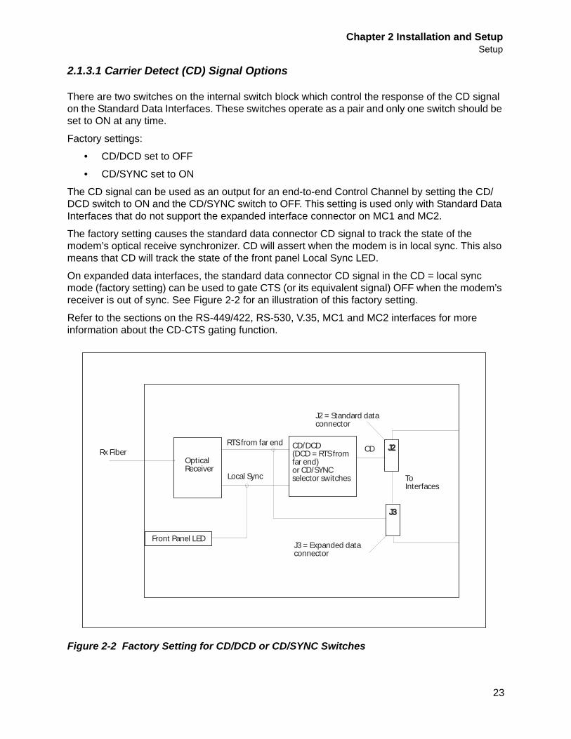
2.1.3.1 Carrier Detect (CD) Signal Options
There are two switches on the internal switch block which control the response of the CD signal on the Standard Data Interfaces. These switches operate as a pair and only one switch should be set to ON at any time.
Factory settings:
• CD/DCD set to OFF
• CD/SYNC set to ON
The CD signal can be used as an output for an end-to-end Control Channel by setting the CD/DCD switch to ON and the CD/SYNC switch to OFF. This setting is used only with Standard Data Interfaces that do not support the expanded interface connector on MC1 and MC2.
The factory setting causes the standard data connector CD signal to track the state of the modem’s optical receive synchronizer. CD will assert when the modem is in local sync. This also means that CD will track the state of the front panel Local Sync LED.
On expanded data interfaces, the standard data connector CD signal in the CD = local sync mode (factory setting) can be used to gate CTS (or its equivalent signal) OFF when the modem’s receiver is out of sync. See Figure 2-2 for an illustration of this factory setting.
Refer to the sections on the RS-449/422, RS-530, V.35, MC1 and MC2 interfaces for more information about the CD-CTS gating function.
Figure 2-2 Factory Setting for CD/DCD or CD/SYNC Switches
CD/DCD (DCD = RTS fromfar end)or CD/SYNCselector switches
OpticalReceiver
Rx Fiber
Front Panel LED
J2
J3
ToInterfaces
J2 = Standard dataconnector
J3 = Expanded dataconnector
RTS from far end
Local Sync
CD
2240 Fiber Optic Modem User Manual Chapter 2 Installation and SetupSetup
24
2.1.3.2 Internal Clock Option Switches
There are two switches on the Internal switch block which affect the operation of the Clock circuits:
• TBL/NORM
• CLK/EXT
2.1.3.3 TBL/NORM Switch
The TBL/NORM switch controls the Data Rate Table as indicated in Table 3-4.
It is configured as ON when shipped from the factory. If it is switched to OFF, the alternate Divide Ratios become active.
Factory setting: ON
2.1.3.4 CLK/EXT Switch
The CLK/EXT switch controls which clock is used for synchronous input. If it is switched to ON, any mode which sources Send Timing (Internal or Slave) will use a turned-around clock coming in on Terminal Timing from the user's equipment. This compensates for round-trip delays in the sourced clock which could otherwise shift the clock-data phasing of the transmit signal and cause errors. This setting can only be used where leads for both are available, and if the user's equipment can turn the Send Timing back around onto the Terminal Timing leads, either internally or at the other end of the cable.
NOTE: The ON setting of the CLK/EXT switch is required for operating redundant modems using either internal or slave clocking.
Factory setting: OFF
2.1.4 Signal Ground StrapThe jumper selects whether chassis ground is connected directly to signal ground (CHASSIS position) or signal ground is separated from chassis ground (FLOAT position).
NOTE: Float can be overridden by chassis ground jumpers on interface cards or by a jumper in the 2201 Rack Chassis.
NOTE: When installed in the 2201 rack chassis, any modem main board, interface, or rack chassis jumper being set to SHORT will override the FLOAT and 100_OHM positions on all of the other modems. CONSIDER THIS JUMPER CAREFULLY.
Factory setting: FLOAT
2.1.5 SCT Normal/Invert JumperThis jumper allows the SCT output from the 2240 to be normal phase or inverted phase. The purpose of this jumper is to allow compensation for round trip transmit clock/transmit data phase delays in situations where the customer equipment can not return SCT as SCTE. For more information about transmit clock, data phasing and SCTE use, see section 3.6 and section 3.7.
Chapter 2 Installation and SetupSetup
25
In the NORM position the 2240 samples TXD at the clock edge corresponding to the appropriate standards, i.e., the 2240 samples TXD at the SCT A lead FALLING edge.
In the INV (invert) position the 2240 samples TXD at the clock edge opposite of the appropriate standards, i.e., the 2240 samples TXD at the SCT A lead RISING edge.
Factory setting: NORM
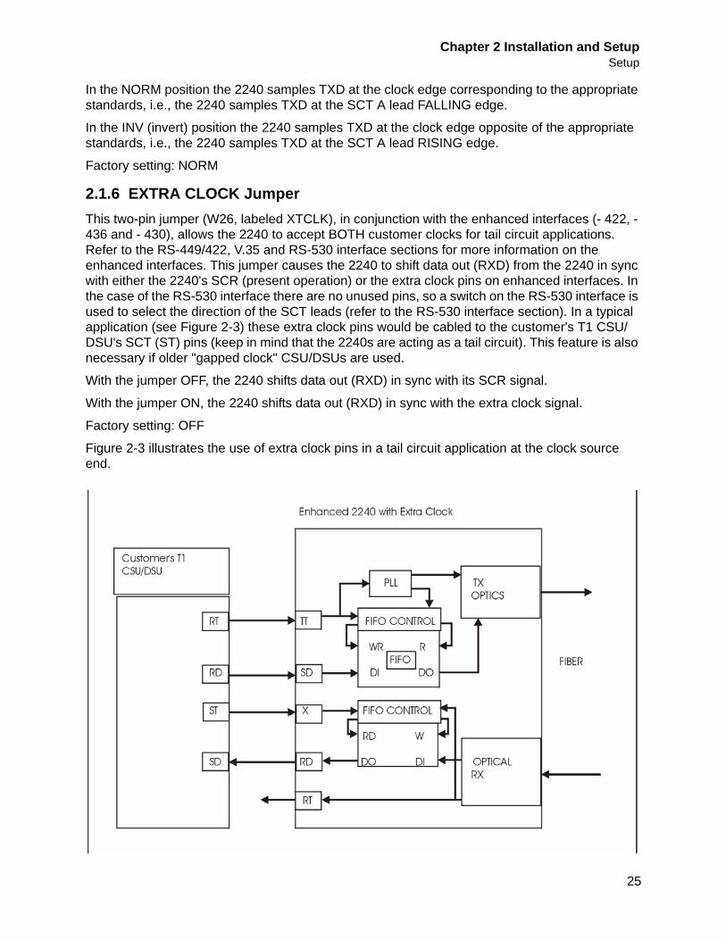
2.1.6 EXTRA CLOCK JumperThis two-pin jumper (W26, labeled XTCLK), in conjunction with the enhanced interfaces (- 422, - 436 and - 430), allows the 2240 to accept BOTH customer clocks for tail circuit applications. Refer to the RS-449/422, V.35 and RS-530 interface sections for more information on the enhanced interfaces. This jumper causes the 2240 to shift data out (RXD) from the 2240 in sync with either the 2240's SCR (present operation) or the extra clock pins on enhanced interfaces. In the case of the RS-530 interface there are no unused pins, so a switch on the RS-530 interface is used to select the direction of the SCT leads (refer to the RS-530 interface section). In a typical application (see Figure 2-3) these extra clock pins would be cabled to the customer's T1 CSU/DSU's SCT (ST) pins (keep in mind that the 2240s are acting as a tail circuit). This feature is also necessary if older "gapped clock" CSU/DSUs are used.
With the jumper OFF, the 2240 shifts data out (RXD) in sync with its SCR signal.
With the jumper ON, the 2240 shifts data out (RXD) in sync with the extra clock signal.
Factory setting: OFF
Figure 2-3 illustrates the use of extra clock pins in a tail circuit application at the clock source end.
2240 Fiber Optic Modem User Manual Chapter 2 Installation and SetupSetup
26
Figure 2-3 Extra Clock Pins in a Tail Circuit Application at Clock Source End
NOTE: X equals the extra clock input pins on the enhanced interfaces. "Extra clock" jumper would have to be ON at this 2240.
NOTE: Control lead crossovers are not shown for clarity.
NOTE: The 2240 in the diagram would be operating in Mode 7, with rate set to match CSU/DSU speed. The 2240 at far end would be operating in slave mode.
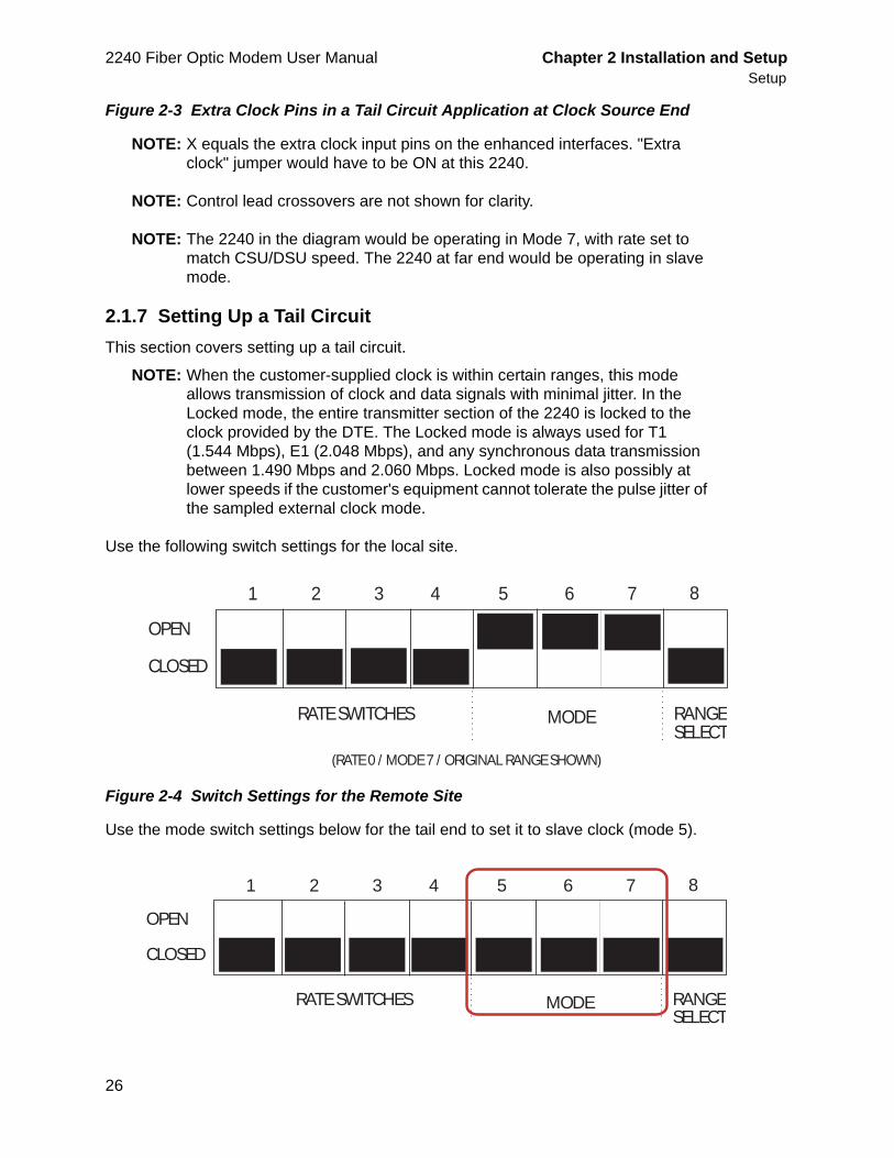
2.1.7 Setting Up a Tail CircuitThis section covers setting up a tail circuit.
NOTE: When the customer-supplied clock is within certain ranges, this mode allows transmission of clock and data signals with minimal jitter. In the Locked mode, the entire transmitter section of the 2240 is locked to the clock provided by the DTE. The Locked mode is always used for T1 (1.544 Mbps), E1 (2.048 Mbps), and any synchronous data transmission between 1.490 Mbps and 2.060 Mbps. Locked mode is also possibly at lower speeds if the customer's equipment cannot tolerate the pulse jitter of the sampled external clock mode.
Use the following switch settings for the local site.
Figure 2-4 Switch Settings for the Remote Site
Use the mode switch settings below for the tail end to set it to slave clock (mode 5).
1 73 4 5 6 82
OPEN
CLOSED
RATE SWITCHES MODE RANGESELECT
(RATE 0 / MODE 7 / ORIGINAL RANGE SHOWN)
1 73 4 5 6 82
OPEN
CLOSED
RATE SWITCHES MODE RANGESELECT
Chapter 2 Installation and SetupInstallation
27
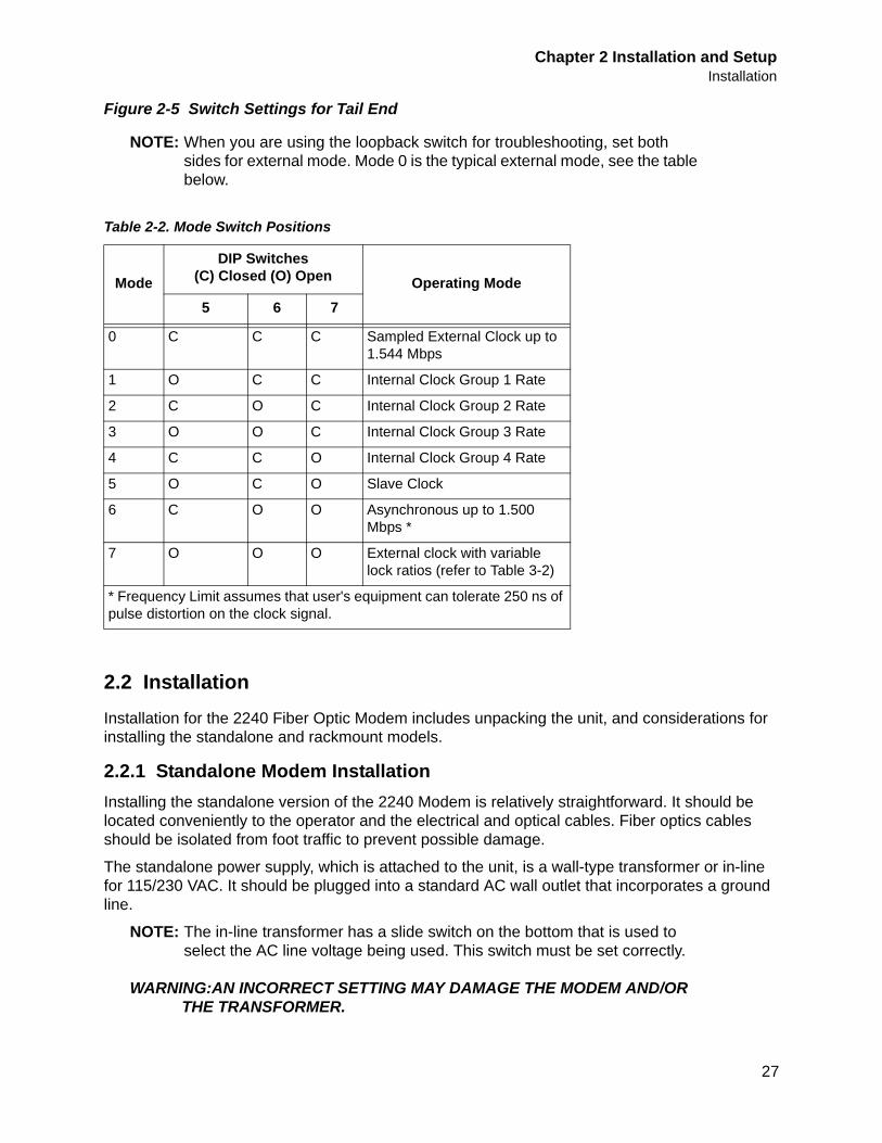
Figure 2-5 Switch Settings for Tail End
NOTE: When you are using the loopback switch for troubleshooting, set both sides for external mode. Mode 0 is the typical external mode, see the table below.
2.2 InstallationInstallation for the 2240 Fiber Optic Modem includes unpacking the unit, and considerations for installing the standalone and rackmount models.
2.2.1 Standalone Modem InstallationInstalling the standalone version of the 2240 Modem is relatively straightforward. It should be located conveniently to the operator and the electrical and optical cables. Fiber optics cables should be isolated from foot traffic to prevent possible damage.
The standalone power supply, which is attached to the unit, is a wall-type transformer or in-line for 115/230 VAC. It should be plugged into a standard AC wall outlet that incorporates a ground line.
NOTE: The in-line transformer has a slide switch on the bottom that is used to select the AC line voltage being used. This switch must be set correctly.
WARNING:AN INCORRECT SETTING MAY DAMAGE THE MODEM AND/OR THE TRANSFORMER.
Table 2-2. Mode Switch Positions
ModeDIP Switches
(C) Closed (O) Open Operating Mode5 6 7
0 C C C Sampled External Clock up to 1.544 Mbps
1 O C C Internal Clock Group 1 Rate
2 C O C Internal Clock Group 2 Rate
3 O O C Internal Clock Group 3 Rate
4 C C O Internal Clock Group 4 Rate
5 O C O Slave Clock
6 C O O Asynchronous up to 1.500 Mbps *
7 O O O External clock with variable lock ratios (refer to Table 3-2)
* Frequency Limit assumes that user's equipment can tolerate 250 ns of pulse distortion on the clock signal.
Chapter 2 Installation and Setup 2240 Fiber Optic Modem User ManualInstallation
28
2.2.2 Rack-Mount Modem InstallationThe 2201 Rack Chassis is designed for installation in a standard 19-inch wide equipment rack. Tabs are provided on each side of the unit, and are predrilled for standard spacing. Refer to the 2201 Rack Chassis User Manual for more information on installing a 2201.
When installing a modem or panel, the Nylatch retainer should be in an outward, or released condition. Slide the modem card into the rack until it engages fully with the PC board edge connector, then push the Nylatch retainers in.
For each modem installed, compatible communications cables and appropriate fiber optic cables, terminated with the appropriate type connectors, will be required.
2.2.3 Fiber Cable and ConnectorsThe Transmit (Tx) from the local modem should be connected to the Receive (Rx) at the remote modem and the Receive (Rx) from the local modem should be connected to the Transmit (Tx) at the remote modem.
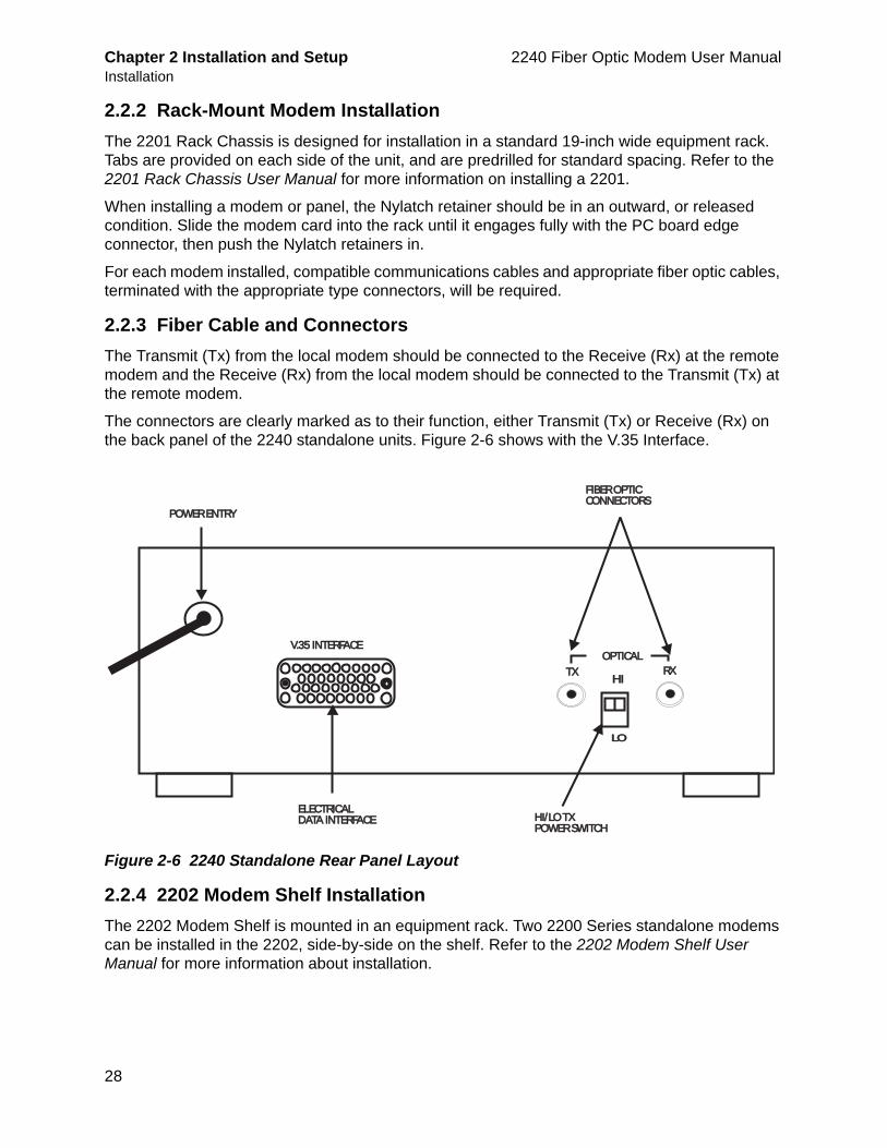
The connectors are clearly marked as to their function, either Transmit (Tx) or Receive (Rx) on the back panel of the 2240 standalone units. Figure 2-6 shows with the V.35 Interface.
Figure 2-6 2240 Standalone Rear Panel Layout
2.2.4 2202 Modem Shelf InstallationThe 2202 Modem Shelf is mounted in an equipment rack. Two 2200 Series standalone modems can be installed in the 2202, side-by-side on the shelf. Refer to the 2202 Modem Shelf User Manual for more information about installation.
OPTICALOPTICAL
HIHI
LOLO
TXTX RXRX
V.35 INTERFACEV.35 INTERFACE
POWER ENTRYPOWER ENTRY
ELECTRICALELECTRICALDATA INTERFACEDATA INTERFACE HI/LO TXHI/LO TX
POWER SWITCHPOWER SWITCH
FIBER OPTICFIBER OPTICCONNECTORSCONNECTORS
Chapter 2 Installation and SetupInstallation
29
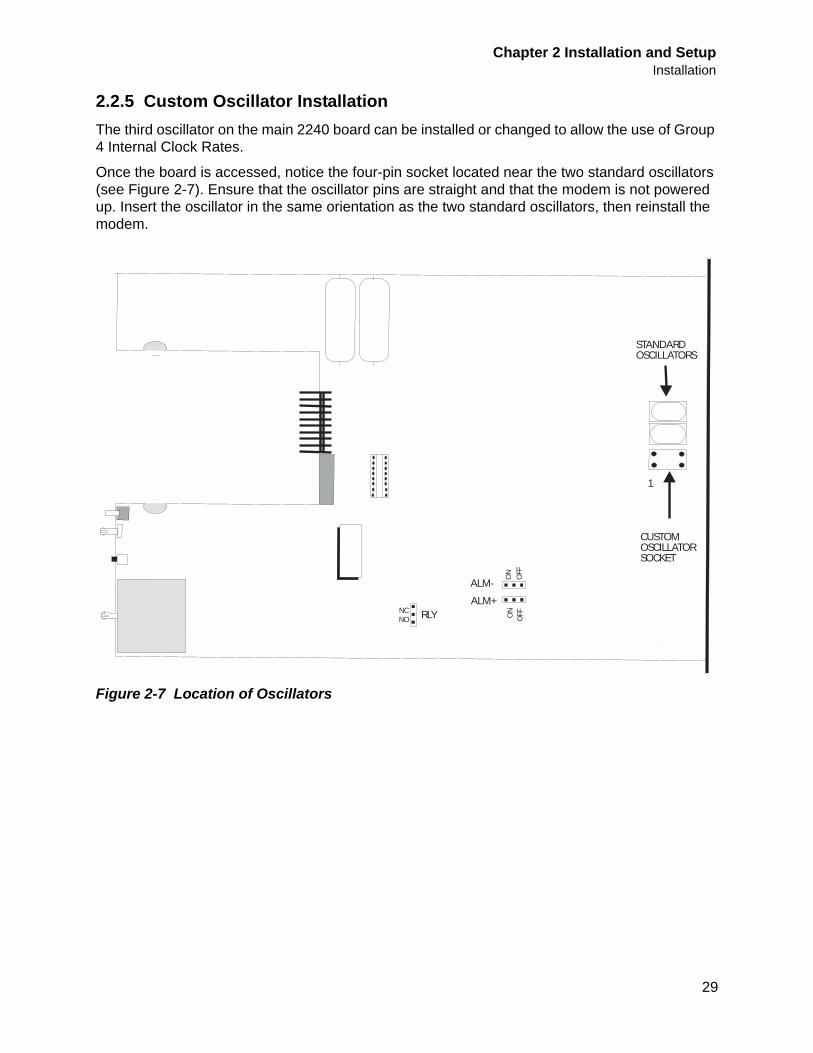
2.2.5 Custom Oscillator InstallationThe third oscillator on the main 2240 board can be installed or changed to allow the use of Group 4 Internal Clock Rates.
Once the board is accessed, notice the four-pin socket located near the two standard oscillators (see Figure 2-7). Ensure that the oscillator pins are straight and that the modem is not powered up. Insert the oscillator in the same orientation as the two standard oscillators, then reinstall the modem.
Figure 2-7 Location of Oscillators
NCNO
ON
OFF
ON
OFFRLY
ALM+
ALM-
1
STANDARDOSCILLATORS
CUSTOMOSCILLATORSOCKET

Chapter 2 Installation and Setup 2240 Fiber Optic Modem User ManualInstallation
30
31
Chapter 3
Mode and Rate Selection
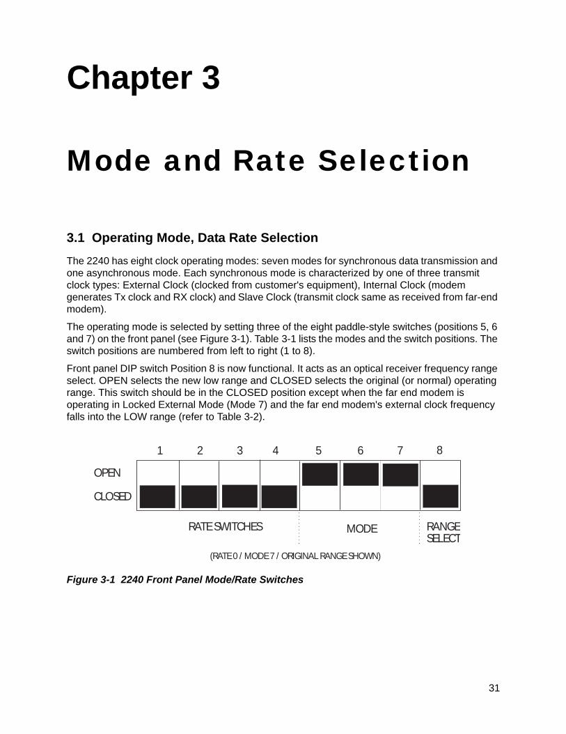
3.1 Operating Mode, Data Rate SelectionThe 2240 has eight clock operating modes: seven modes for synchronous data transmission and one asynchronous mode. Each synchronous mode is characterized by one of three transmit clock types: External Clock (clocked from customer's equipment), Internal Clock (modem generates Tx clock and RX clock) and Slave Clock (transmit clock same as received from far-end modem).
The operating mode is selected by setting three of the eight paddle-style switches (positions 5, 6 and 7) on the front panel (see Figure 3-1). Table 3-1 lists the modes and the switch positions. The switch positions are numbered from left to right (1 to 8).
Front panel DIP switch Position 8 is now functional. It acts as an optical receiver frequency range select. OPEN selects the new low range and CLOSED selects the original (or normal) operating range. This switch should be in the CLOSED position except when the far end modem is operating in Locked External Mode (Mode 7) and the far end modem's external clock frequency falls into the LOW range (refer to Table 3-2).
Figure 3-1 2240 Front Panel Mode/Rate Switches
1 73 4 5 6 82
OPEN
CLOSED
RATE SWITCHES MODE RANGESELECT
(RATE 0 / MODE 7 / ORIGINAL RANGE SHOWN)
2240 Fiber Optic Modem User Manual Chapter 3 Mode and Rate SelectionOperating Mode, Data Rate Selection
32
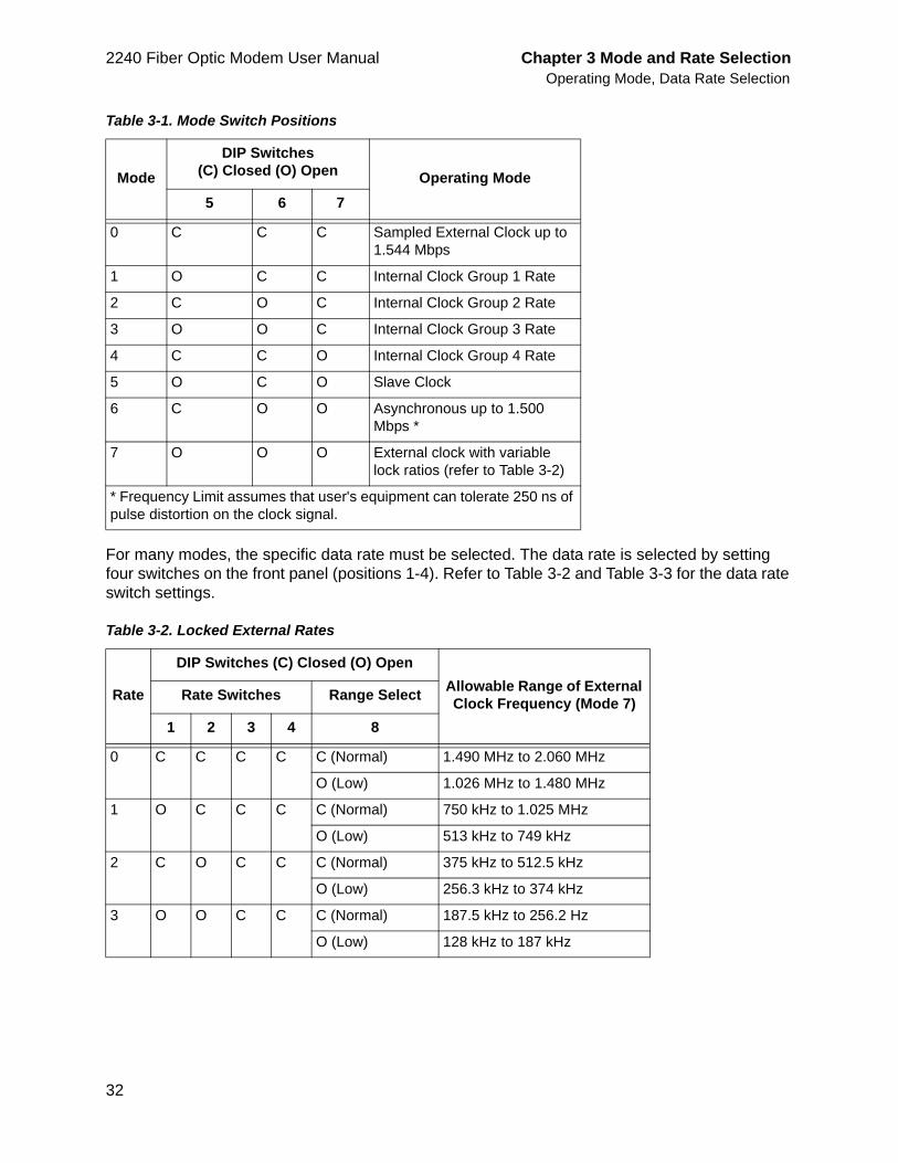
For many modes, the specific data rate must be selected. The data rate is selected by setting four switches on the front panel (positions 1-4). Refer to Table 3-2 and Table 3-3 for the data rate switch settings.
Table 3-1. Mode Switch Positions
ModeDIP Switches
(C) Closed (O) Open Operating Mode5 6 7
0 C C C Sampled External Clock up to 1.544 Mbps
1 O C C Internal Clock Group 1 Rate
2 C O C Internal Clock Group 2 Rate
3 O O C Internal Clock Group 3 Rate
4 C C O Internal Clock Group 4 Rate
5 O C O Slave Clock
6 C O O Asynchronous up to 1.500 Mbps *
7 O O O External clock with variable lock ratios (refer to Table 3-2)
* Frequency Limit assumes that user's equipment can tolerate 250 ns of pulse distortion on the clock signal.
Table 3-2. Locked External Rates
Rate
DIP Switches (C) Closed (O) OpenAllowable Range of External Clock Frequency (Mode 7)Rate Switches Range Select
1 2 3 4 8
0 C C C C C (Normal) 1.490 MHz to 2.060 MHz
O (Low) 1.026 MHz to 1.480 MHz
1 O C C C C (Normal) 750 kHz to 1.025 MHz
O (Low) 513 kHz to 749 kHz
2 C O C C C (Normal) 375 kHz to 512.5 kHz
O (Low) 256.3 kHz to 374 kHz
3 O O C C C (Normal) 187.5 kHz to 256.2 Hz
O (Low) 128 kHz to 187 kHz
Chapter 3 Mode and Rate SelectionExternal Clock Modes
33
3.2 External Clock ModesThe external clock modes are used when it is necessary to have the DTE provide the transmit clock or when the 2240 is used as a tail circuit connecting to a DCE. In these modes, the DTE or DCE sends this clock to the modem on the Terminal Timing (TT) or equivalent signal leads. For an example of a typical complete tail circuit, refer to section 3.4. There are two different types of External Clock Modes in the 2240: Sampled and Locked.
NOTE: Interfaces which extract the clock from a composite signal, such as T1 or E1, require the use of the Locked External Clock Mode.
3.2.1 Sampled External Clock Mode - Mode 0In this mode, the 2240 transmits an 8.192 Mbps optical composite signal which is derived from an internal oscillator. One half of the composite bandwidth is used to send the clock signal which is sampled at 4.096 MHz. One fourth of the composite bandwidth is used to send the data signal which is sampled at 2.048 MHz. This sampling results in 244 nanoseconds of pulse distortion on the clock received at the other modem. The distortion is a result of the sampling process. The maximum data rate is limited to 1.544 Mbps where the distortion is 37% of the clock period.
NOTE: The pulse distortion is 37% of the bit period at a data rate of 1.544 Mbps. When using this operating mode, it is important to consider the effect of this large distortion on the connected equipment.
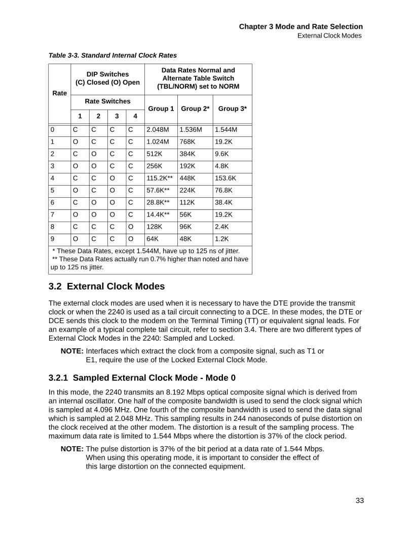
Table 3-3. Standard Internal Clock Rates
Rate
DIP Switches(C) Closed (O) Open
Data Rates Normal and Alternate Table Switch
(TBL/NORM) set to NORM
Rate SwitchesGroup 1 Group 2* Group 3*
1 2 3 4
0 C C C C 2.048M 1.536M 1.544M
1 O C C C 1.024M 768K 19.2K
2 C O C C 512K 384K 9.6K
3 O O C C 256K 192K 4.8K
4 C C O C 115.2K** 448K 153.6K
5 O C O C 57.6K** 224K 76.8K
6 C O O C 28.8K** 112K 38.4K
7 O O O C 14.4K** 56K 19.2K
8 C C C O 128K 96K 2.4K
9 O C C O 64K 48K 1.2K
* These Data Rates, except 1.544M, have up to 125 ns of jitter. ** These Data Rates actually run 0.7% higher than noted and have up to 125 ns jitter.
2240 Fiber Optic Modem User Manual Chapter 3 Mode and Rate SelectionInternal Clock Modes - Modes 1, 2, 3, 4
34
Sampled External Clock Mode does not use the Rate Switches.
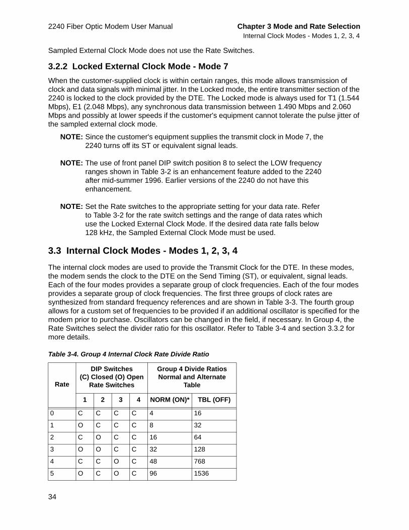
3.2.2 Locked External Clock Mode - Mode 7When the customer-supplied clock is within certain ranges, this mode allows transmission of clock and data signals with minimal jitter. In the Locked mode, the entire transmitter section of the 2240 is locked to the clock provided by the DTE. The Locked mode is always used for T1 (1.544 Mbps), E1 (2.048 Mbps), any synchronous data transmission between 1.490 Mbps and 2.060 Mbps and possibly at lower speeds if the customer's equipment cannot tolerate the pulse jitter of the sampled external clock mode.
NOTE: Since the customer's equipment supplies the transmit clock in Mode 7, the 2240 turns off its ST or equivalent signal leads.
NOTE: The use of front panel DIP switch position 8 to select the LOW frequency ranges shown in Table 3-2 is an enhancement feature added to the 2240 after mid-summer 1996. Earlier versions of the 2240 do not have this enhancement.
NOTE: Set the Rate switches to the appropriate setting for your data rate. Refer to Table 3-2 for the rate switch settings and the range of data rates which use the Locked External Clock Mode. If the desired data rate falls below 128 kHz, the Sampled External Clock Mode must be used.
3.3 Internal Clock Modes - Modes 1, 2, 3, 4The internal clock modes are used to provide the Transmit Clock for the DTE. In these modes, the modem sends the clock to the DTE on the Send Timing (ST), or equivalent, signal leads. Each of the four modes provides a separate group of clock frequencies. Each of the four modes provides a separate group of clock frequencies. The first three groups of clock rates are synthesized from standard frequency references and are shown in Table 3-3. The fourth group allows for a custom set of frequencies to be provided if an additional oscillator is specified for the modem prior to purchase. Oscillators can be changed in the field, if necessary. In Group 4, the Rate Switches select the divider ratio for this oscillator. Refer to Table 3-4 and section 3.3.2 for more details.
Table 3-4. Group 4 Internal Clock Rate Divide Ratio
Rate
DIP Switches(C) Closed (O) Open
Rate Switches
Group 4 Divide RatiosNormal and Alternate
Table
1 2 3 4 NORM (ON)* TBL (OFF)
0 C C C C 4 16
1 O C C C 8 32
2 C O C C 16 64
3 O O C C 32 128
4 C C O C 48 768
5 O C O C 96 1536
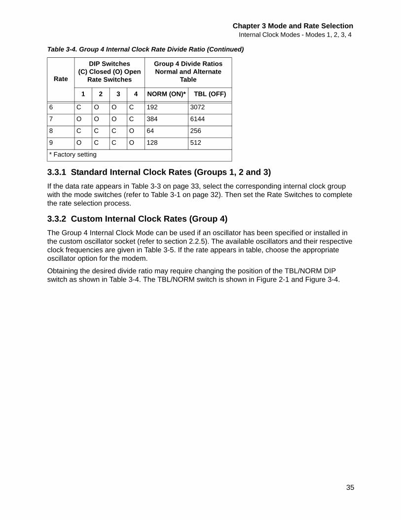
Chapter 3 Mode and Rate SelectionInternal Clock Modes - Modes 1, 2, 3, 4
35
3.3.1 Standard Internal Clock Rates (Groups 1, 2 and 3)If the data rate appears in Table 3-3 on page 33, select the corresponding internal clock group with the mode switches (refer to Table 3-1 on page 32). Then set the Rate Switches to complete the rate selection process.
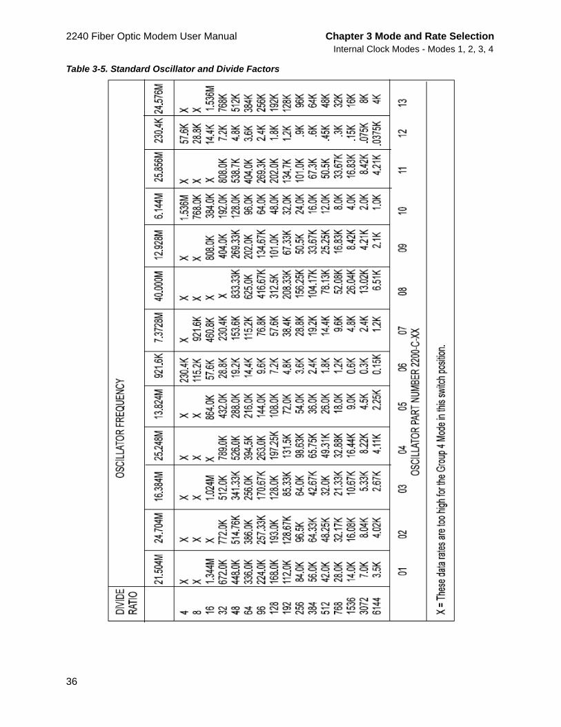
3.3.2 Custom Internal Clock Rates (Group 4)The Group 4 Internal Clock Mode can be used if an oscillator has been specified or installed in the custom oscillator socket (refer to section 2.2.5). The available oscillators and their respective clock frequencies are given in Table 3-5. If the rate appears in table, choose the appropriate oscillator option for the modem.
Obtaining the desired divide ratio may require changing the position of the TBL/NORM DIP switch as shown in Table 3-4. The TBL/NORM switch is shown in Figure 2-1 and Figure 3-4.
6 C O O C 192 3072
7 O O O C 384 6144
8 C C C O 64 256
9 O C C O 128 512
* Factory setting
Table 3-4. Group 4 Internal Clock Rate Divide Ratio (Continued)
Rate
DIP Switches(C) Closed (O) Open
Rate Switches
Group 4 Divide RatiosNormal and Alternate
Table
1 2 3 4 NORM (ON)* TBL (OFF)
2240 Fiber Optic Modem User Manual Chapter 3 Mode and Rate SelectionInternal Clock Modes - Modes 1, 2, 3, 4
36
Table 3-5. Standard Oscillator and Divide Factors
Chapter 3 Mode and Rate SelectionSlave Clock Mode - Mode 5
37
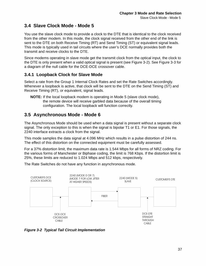
3.4 Slave Clock Mode - Mode 5You use the slave clock mode to provide a clock to the DTE that is identical to the clock received from the other modem. In this mode, the clock signal received from the other end of the link is sent to the DTE on both Receive Timing (RT) and Send Timing (ST) or equivalent signal leads. This mode is typically used in tail circuits where the user’s DCE normally provides both the transmit and receive clocks to the DTE.
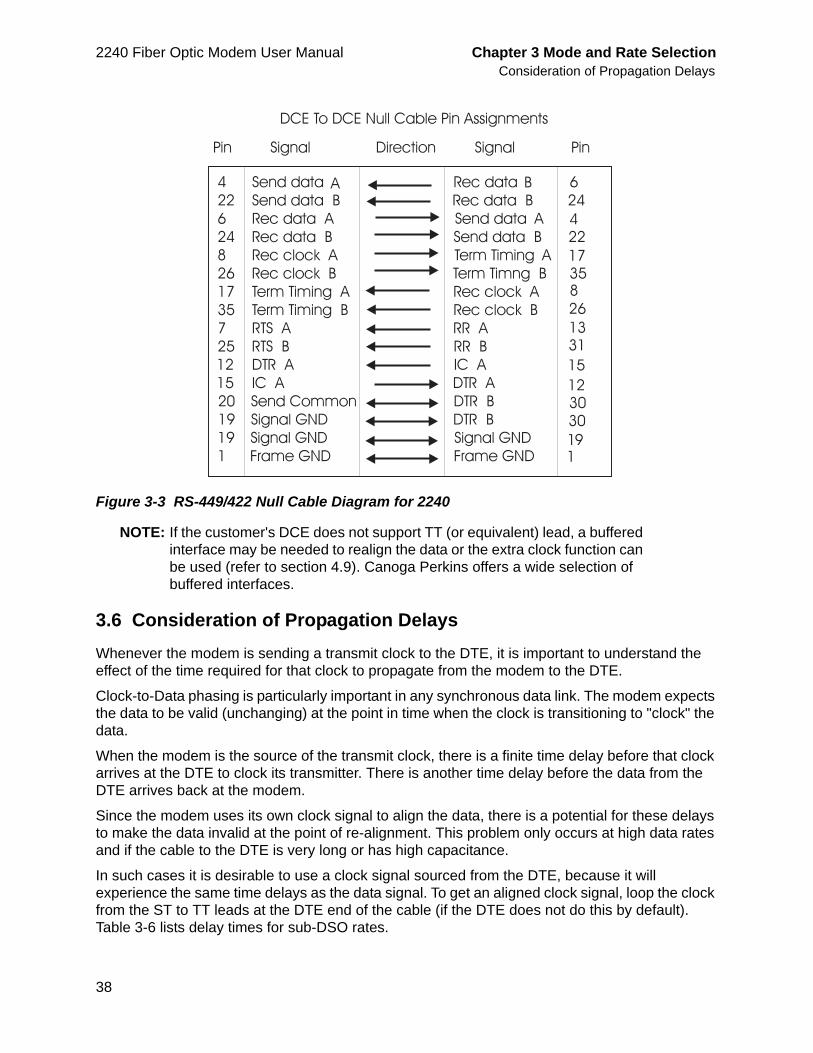
Since modems operating in slave mode get the transmit clock from the optical input, the clock to the DTE is only present when a valid optical signal is present (see Figure 3-2). See Figure 3-3 for a diagram of the null cable for the DCE-DCE crossover cable.
3.4.1 Loopback Clock for Slave ModeSelect a rate from the Group 1 Internal Clock Rates and set the Rate Switches accordingly. Whenever a loopback is active, that clock will be sent to the DTE on the Send Timing (ST) and Receive Timing (RT), or equivalent, signal leads.
NOTE: If the local loopback modem is operating in Mode 5 (slave clock mode), the remote device will receive garbled data because of the overall timing configuration. The local loopback will function correctly.
3.5 Asynchronous Mode - Mode 6 The Asynchronous Mode should be used when a data signal is present without a separate clock signal. The only exception to this is when the signal is bipolar T1 or E1. For those signals, the 2240 interface extracts a clock from the signal.
This mode samples the data signal at 4.096 MHz which results in a pulse distortion of 244 ns. The effect of this distortion on the connected equipment must be carefully assessed.
For a 37% distortion limit, the maximum data rate is 1.544 Mbps for all forms of NRZ coding. For the various forms of Manchester or Biphase coding, the limit is 768 Kbps. If the distortion limit is 25%, these limits are reduced to 1.024 Mbps and 512 kbps, respectively.
The Rate Switches do not have any function in asynchronous mode.
Figure 3-2 Typical Tail Circuit Implementation
2240 Fiber Optic Modem User Manual Chapter 3 Mode and Rate SelectionConsideration of Propagation Delays
38
Figure 3-3 RS-449/422 Null Cable Diagram for 2240
NOTE: If the customer's DCE does not support TT (or equivalent) lead, a buffered interface may be needed to realign the data or the extra clock function can be used (refer to section 4.9). Canoga Perkins offers a wide selection of buffered interfaces.
3.6 Consideration of Propagation DelaysWhenever the modem is sending a transmit clock to the DTE, it is important to understand the effect of the time required for that clock to propagate from the modem to the DTE.
Clock-to-Data phasing is particularly important in any synchronous data link. The modem expects the data to be valid (unchanging) at the point in time when the clock is transitioning to "clock" the data.
When the modem is the source of the transmit clock, there is a finite time delay before that clock arrives at the DTE to clock its transmitter. There is another time delay before the data from the DTE arrives back at the modem.
Since the modem uses its own clock signal to align the data, there is a potential for these delays to make the data invalid at the point of re-alignment. This problem only occurs at high data rates and if the cable to the DTE is very long or has high capacitance.
In such cases it is desirable to use a clock signal sourced from the DTE, because it will experience the same time delays as the data signal. To get an aligned clock signal, loop the clock from the ST to TT leads at the DTE end of the cable (if the DTE does not do this by default). Table 3-6 lists delay times for sub-DSO rates.
Chapter 3 Mode and Rate SelectionInternal Clock Option Switches
39
NOTE: The 2240 can be made to use the TT signal for realigning the data by turning ON the CLK/EXT switch on the main board. This switch is position 7 of the internal options switches, as illustrated in Figure 2-1 and Figure 3-4. It is set to the OFF position when shipped from the factory.
3.7 Internal Clock Option SwitchesThere are two switches on the Internal switch block which affect the operation of the Clock circuits: TBL/NORM and CLK/EXT (see Figure 2-1 and Figure 3-4 for the locations of these switches).
3.7.1 TBL/NORM SwitchThe TBL/NORM switch controls the Data Rate Table as indicated in Table 3-4.
It is configured as ON when shipped from the factory. If it is switched to OFF, the alternate Divide Ratios become active.
Factory setting: ON
3.7.2 CLK/EXT SwitchThe CLK/EXT switch controls which clock is used for synchronous input. If it is switched to ON, any mode which sources Send Timing (Internal or Slave) will use a turned-around clock coming in on Terminal Timing from the user's equipment. This compensates for round-trip delays in the sourced clock which could otherwise shift the clock-data phasing of the transmit signal and cause errors. This setting can only be used where leads for both are available, and if the user's equipment can turn the Send Timing back around onto the Terminal Timing leads, either internally or at the other end of the cable.
NOTE: The ON setting of the CLK/EXT switch is required for operating redundant modems using either internal or slave clocking.
NOTE: On standalone models, these switches can only be accessed after the top cover has been removed. The cover is fastened by screws on the sides of the case. If the modem is mounted in a 2202 Modem Shelf, it must first be
Table 3-6. Delay Time Through Model 2240 at Sub-DSO Rates
Sampled External Clock Frequency Delay
2.4 KHz 417 ms
4.8 KHz 208 ms
9.6 KHz 104 ms
19.2 KHz 52 ms
38.4 KHz 26 ms
56 KHz 18 ms
64 KHz 16 ms
Chapter 3 Mode and Rate Selection 2240 Fiber Optic Modem User ManualInternal Clock Option Switches
40
removed from the shelf. Be sure to disconnect power before removing the cover.
Factory setting: OFF
Figure 3-4 Location of Internal Switches and Jumpers (factory settings are illustrated)
INTE
RNA
L O
PTIO
NSW
ITC
HES
FAC
TORY
SET
OFF O
N
OFF
OFF ON
OFF
OFF ON
OFF
ON
CD
/DC
D
CD
/SY
NC
ALM
/CH
AN
ALM
/LO
C
ALM
/REM
ALM
/IN
V
CLK
/EX
T
TBL/
NO
RM
INTE
RNA
LO
PTIO
NSW
ITC
HES RE
LAY
OPT
ION
JUM
PER
CO
NTA
CT
POW
ERJU
MPE
RS
EXPA
ND
ED IN
TERF
AC
EC
ON
NEC
TOR
NC
NO
ON
OFFON
OFF
STA
ND
ARD
INTE
RFA
CE
CO
NN
ECTO
R
AU
XIN
TERF
AC
EC
ON
NEC
TOR
HI/
LOW
OPT
ICS
POW
ER S
WIT
CH
ES
OSC
ILLA
TOR
3 LO
CAT
ION
RLY
ALM
+
ALM
-
SCT
CLO
CK
PHA
SE
EXTR
A C
LOC
K
NO
RMR
TS
TX O
PT
CH
ASS
ISFL
OAT
SIG
NA
L G
ROU
ND
JU
MPE
R
RES.
FO
RFU
TURE
USE
NO
RM
INV
41
Chapter 4
Data Interfaces
4.1 Data Interfaces OverviewA variety of interfaces is available for the 2240 Modem:
Each interface conforms to existing standards. For applicable standards and physical connector types, See Chapter 7, "Specifications". Refer to section 7.5 for a list of available interface options.
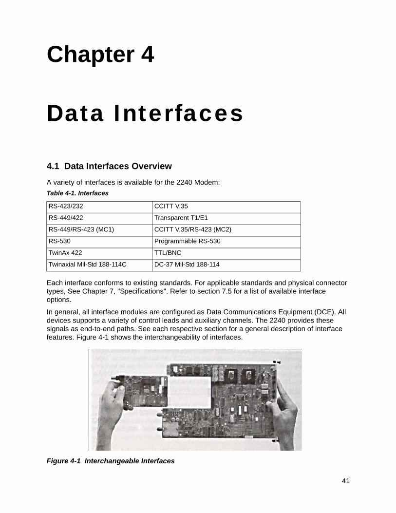
In general, all interface modules are configured as Data Communications Equipment (DCE). All devices supports a variety of control leads and auxiliary channels. The 2240 provides these signals as end-to-end paths. See each respective section for a general description of interface features. Figure 4-1 shows the interchangeability of interfaces.
Figure 4-1 Interchangeable Interfaces
Table 4-1. Interfaces
RS-423/232 CCITT V.35
RS-449/422 Transparent T1/E1
RS-449/RS-423 (MC1) CCITT V.35/RS-423 (MC2)
RS-530 Programmable RS-530
TwinAx 422 TTL/BNC
Twinaxial Mil-Std 188-114C DC-37 Mil-Std 188-114
2240 Fiber Optic Modem User Manual Chapter 4 Data InterfacesRS-423/232D Model 432
42
4.2 RS-423/232D Model 432NOTE: The maximum data rate for this interface, 153.6 Kbps, is limited by the
interface driver slew rate.
This interface is electrically compatible with EIA RS-423A. It will also operate with RS-232D systems when adhering to the more limiting RS-232D specifications (20 kbps and 2500 pF cable capacitance). EIA standard RS-423A does not reference physical connector types or pinouts.
This interface uses the physical connector type and pinouts specified in RS-232D (refer to Table 4-2). The RS-423/232D interface uses a 25-pin female D-type connector for the physical connection.
The TD, RD, SCT, SCR and SCTE pins carry the primary clock and data signals. The remaining pins are either ground references or control signals.
Transmit Data (TD) and Receive Data (RD) are the data input and output signals for the modem. Serial Clock Transmit (SCT) is the modem’s transmit clock output used for the internal and slave modes. Serial Clock Receive (SCR) is always the clock signal for the Receive Data. Serial Clock Transmit External (SCTE) is the clock signal input used in External Clock Mode.
None of the control leads interact with the data transmission. The control leads are provided in order to comply with a variety of DTE interface requirements. Most of the control leads are actually end-to-end signal channels which can be used for any purpose as long as it conforms to the electrical interface standards of RS-232D or RS-423A. One example of this would be asynchronous data transmission at rates up to 19.2 kbps (30% jitter due to sampling at 64 kHz).
The RTS, CTS and DCD pins function together to provide the most common handshake functions. An input to RTS (see description of RTS-Bias jumper) is transmitted to the DCD output at the other end of the link (see description of DCD jumper). CTS follows RTS locally but it is delayed by approximately 1 msec when RTS turns ON (see description of CTS-Gate jumper).
There are four other end-to-end control lead pairs. They are listed below with the input signal listed first:
• STD to SRD
• SRTS to SDCD
• DTR to RI
• DSRS to SCTS
Table 4-2. RS-232D Pinouts
Pin Number
RS-232D Pin Name (abbrev)
Full Name Direction
1 PG Protective Ground -
2 TD Transmit Data to modem
3 RD Receive Data from modem
4 RTS Request to Send to modem
5 CTS Clear to Send from modem
Chapter 4 Data InterfacesRS-423/232D Model 432
43
Data Set Ready (DSR) and Test Mode (TM) are local status leads and follow the functions described in RS-232D. DSR typically indicates that the modem is ready to handle transmit data. During loopbacks, the behavior of this signal is dependent on the position of the DSR jumper (see description of DSR jumper). TM indicates that a loopback is active on one or both modems.
Local Loopback (LL) and Remote Loopback (RL) are loopback control leads and perform the same functions as the 2240 front panel LOOP switch LOC and REM positions. LL and RL are interface signal inputs which can be used to activate the LOC or REM loop functions.
RTS_BIAS Jumper
The RTS_BIAS jumper controls the state that RTS floats to when there is no signal driving the RTS pin. The OFF position forces this signal to the OFF (negated) state when the interface cable is disconnected. The ON position forces it to the ON (asserted) state.
Factory setting: OFF
4.2.1 DCD JumperThe DCD Jumper determines the source of the DCD output. In the CTRL position, the DCE output functions as the output for the RTS input at the far end. In the CD jumper position and with local RTS ON, CTS will turn ON either when the modem's fiber optic receiver is in sync (main PCBA internal switch S1 CD/DCD = OFF and CD/SYNC = ON) or the state of the RTS signal at
6 DSR DCE Ready from modem
7 SG Signal Ground -
8 DCD Receive Line Sig. Det. from modem
12 SDCD Secondary Line Sig. Det. from modem
13 SCTS Secondary CTS from modem
14 STD Secondary TD to modem
15 SCT Transmit Clock from modem
16 SRD Secondary RD from modem
17 SCR Receive Clock from modem
18 LL Local Loopback to modem
19 SRTS Secondary RTS to modem
20 DTR DTE Ready to modem
21 RL Remote Loopback to modem
22 RI Ring Indicator from modem
23 DSRS Data Signal Rate Selector to modem
24 SCTE Transmit Clock External to modem
25 TM Test Mode from modem
Table 4-2. RS-232D Pinouts (Continued)
Pin Number
RS-232D Pin Name (abbrev)
Full Name Direction
2240 Fiber Optic Modem User Manual Chapter 4 Data InterfacesRS-449/422 Model 422
44
the far end (main PCBA internal switch S1 CD/DCD = ON and CD/SYNC = OFF). Refer to section 2.1.3.1 for more information on the internal switch S1 CD/DCD and CD/SYNC positions.
Factory setting: CTRL
4.2.2 CTS_GATE JumperThe CTS_GATE jumper controls the state of CTS when the local RTS is ON. When the jumper is in the ON position, CTS follows RTS only. The CD position allows the 2240's standard data interface signal CD to gate CTS. In the CD jumper position and with local RTS ON, CTS will turn ON either when the modem's fiber optic receiver is in sync (main PCBA internal switch S1 CD/DCD = OFF and CD/SYNC = ON) or the RTS signal at the far end is ON (main PCBA internal switch S1 CD/DCD = ON and CD/SYNC = OFF). Refer to section 2.1.3.1 for more information on the internal switch S1 CD/DCD and CD/SYNC positions.
Factory setting: ON
4.2.3 DSR JumperThe DSR jumper controls the behavior of the DSR signal. The EIA position causes the DSR to turn OFF in certain test conditions when the transmit data is blocked and has no end-to-end or loopback path. This condition exists when the far-end 2240 modem has a local loopback active. The TEST position causes DSR to turn OFF (negate) whenever any loopback is active at one or both modems.
Factory setting: EIA
4.2.4 CH_GND JumperThe jumper selects whether chassis ground is connected directly to signal ground (SHORT position) or through a 100 Ohm resistor (100_OHM position).
NOTE: In the standalone model, the 100_OHM position will only put a 100 Ohm resistor between the two grounds if the 2240's main board SIGNAL GND jumper is set to the FLOAT position. When installed in the 2201 Rack Chassis, any modem main board, interface, or rack chassis jumper being set to SHORT will override the FLOAT and 100_OHM positions on all of the other modems. CONSIDER THIS JUMPER CAREFULLY.
Factory setting: 100_OHM
4.3 RS-449/422 Model 422This interface complies with EIA Standard RS-449. Electrical characteristics comply with RS-422 for clock and data signals and RS-423 for control signals.
The RS-449/422 interface applies the physical connector type and pinouts specified in RS-449 (refer to Table 4-3). The interface uses a 37-pin, female D-type connector for the physical connection.
Chapter 4 Data InterfacesRS-449/422 Model 422
45
The SD, RD, ST, RT and TT pins carry the primary data and clock signals (conforming to the RS-449 and RS-422 standards). In addition, an extra clock signal input (conforming to RS-422) is provided to make the 2240/-422 combination more "DTE-like" in tail circuit applications at the clock source end. The remainder of the pins are either ground references or control signals. Send Data (SD) and Receive Data (RD) are the data input and output signals for the modem, respectively.
Send Timing (ST) is the modem’s transmit clock reference output that is used for the internal and slave clock modes. Receive Timing (RT) is the clock signal for the receive data unless the 2240’s
Table 4-3. RS-449 Pinouts
Pin Number
A/B
RS-449 PIN Name
(abbrev)(full name) Direction
1 SHLD shield -
4/22 SD send data to modem
5/23 ST send timing from modem
6/24 RD receive data from modem
7/25 RS request to send to modem
8/26 RT receive timing from modem
9/27 CS clear to send from modem
10 LL local loopback to modem
11/29 DM data mode from modem
12/30 TR terminal ready to modem
13/31 RR receiver ready from modem
14 RL remote loopback to modem
15 IC incoming call from modem
17/35 TT terminal timing to modem
18 TM test mode from modem
19 SG signal ground -
20 RC receive common - (tied to SG)
33 SQ signal quality from modem
34 NS new signal to modem
37 SC send common to modem
2/36* N/A extra clock for receive data
to modem
* The extra clock is an enhancement added to -422 interfaces. Any -422 interface card outfitted with this capability can be identified via the lack of the W16/W15 BAL_CTRL jumper. The W16/W15 jumper was never described in the manual, so do not try to find a reference to it in the manual.
2240 Fiber Optic Modem User Manual Chapter 4 Data InterfacesRS-449/422 Model 422
46
main PCBA W26 (XTCLK) jumper is ON, in which case the Extra Clock input signal is used to shift receive data out from the 2240. Terminal Timing (TT) is the transmit clock signal used in either of the External clock modes or when the main board internal CLK/EXT switch is set to EXT (refer to section 3.7).
The control signal outputs are unbalanced drivers (conforming to the RS-423 Standard). The B-leads of any differential control signal outputs are tied to signal ground to comply with RS-422.
None of the control leads interact with the data transmission. They are provided in order to comply with a variety of DTE interface requirements. Most of the control leads are actually end-to-end signal channels which can be used for any purpose as long as it conforms to the RS-449 interface standards.
Three end-to-end control leads are provided as part of this interface. An input to RS (Request to Send) is transmitted to the RR (Receiver Ready) output at the other end of the link (see description of RS-Bias jumper and RR jumper). CS (Clear to Send) follows RS locally but is delayed approximately 1 millisecond when RS turns ON (see description of CS-Gate jumper). The other two end-to-end control lead pairs are listed below with the input signal listed first:
• TR to IC
• NS to SQ
DM and TM are local status leads and follow the functions described in RS-449. Data Mode (DM) typically indicates that the modem is ready to handle transmit data. During loopbacks, the behavior of this signal is dependent on the position of the DM jumper (see description of DM jumper).
Local Loopback (LL) and Remote Loopback (RL) are loopback control leads and perform the same functions as the 2240 front panel LOOP switch LOC and REM positions. LL and RL are interface signal inputs which can be used to activate the LOC or REM loop functions. These signals can control the loopback functions only if the front panel switch is in the center OFF position.
4.3.1 RS_BIAS JumperThe RS_BIAS jumper controls the state that RS floats to when there is no signal driving the RS pin. The OFF position forces this signal to the OFF (negated) state when the interface cable is disconnected. The ON position forces it to ON (asserted).
Factory setting: OFF
4.3.2 RR JumperThe RR Jumper determines the source of the RR output. In the CTRL position, the RR output functions as the output for the RS input at the far end. In the CD jumper position, the RR output will turn ON either when the modem’s fiber optic receiver is in sync (main PCBA internal switch S1 CD/DCD = OFF and CD/SYNC = ON) or the far end RTS is ON (main PCBA internal switch S1 CD/DCD = ON and CD/SYNC = OFF). Refer to section 2.1.3.1 for more information on the internal switch S1 CD/DCD and CD/SYNC positions.
Factory setting: CTRL
Chapter 4 Data InterfacesRS-530 Interface Model 430
47
4.3.3 CS_GATE JumperThe CS_GATE jumper controls the state of CS when the local RS is ON. When the jumper is in the ON position, CTS follows RS only. The CD position allows the 2240's standard data interface signal CD to gate CS. In the CD jumper position and with local RS ON, CS will turn ON either when the modem's fiber optic receiver is in sync (main PCBA internal switch S1 CD/DCD = OFF and CD/SYNC = ON) or the RTS signal at the far end is ON (main PCBA internal switch S1 CD/DCD = ON and CD/SYNC = OFF). Refer to section 2.1.3.1 for more information on the internal switch S1 CD/DCD and CD/SYNC positions.
Factory setting: ON
4.3.4 DM JumperThe DM jumper controls the behavior of the DM signal. The EIA position turns DM OFF when the far-end 2240 modem has a local loopback active. The TEST position causes DM to turn OFF whenever any loopback is active at one or both modems.
Factory setting: EIA
4.3.5 CH_GND JumperThe jumper selects whether chassis ground is connected directly to signal ground (SHORT position) or through a 100 Ohm resistor (100_OHM position).
NOTE: In the standalone model, the 100_OHM position will only put a 100 Ohm resistor between the two grounds if the 2240's main board SIGNAL GND jumper is set to the FLOAT position. When installed in the 2201 Rack Chassis, any modem main board, interface or rack chassis jumper being set to SHORT will override the FLOAT and 100_OHM positions on all of the other modems. CONSIDER THIS JUMPER CAREFULLY.
Factory setting: 100_OHM
4.3.6 UNBAL_REF JumperRS-449 specifies that unbalanced inputs to a DCE are to be referenced to the SC (Send Common) pin. This pin on the DCE is tied to the signal ground of the DTE through the interface cable. If this ground connection is present, and you prefer to use it, move the UNBAL_REF jumpers to SC.
Factory setting: GND
4.4 RS-530 Interface Model 430NOTE: The -430 interface supersedes the previous -R30 interface for 2240
applications. The -430 interface is a superset of the -R30. If exact compatibility with the older -R30 is desired, the DCD jumper can be moved from the factory strapped CTRL setting (end-to-end RTS-DCD control lead pair always enabled) to CD (DCD function selected by main board CD/DCD and CD/SYNC switches).
This interface conforms to EIA RS-530. The interface uses RS-422 (balanced) electrical signals for all interface circuits (data, clock and control), except for the loopback and test mode pins
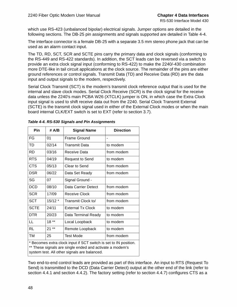
2240 Fiber Optic Modem User Manual Chapter 4 Data InterfacesRS-530 Interface Model 430
48
which use RS-423 (unbalanced bipolar) electrical signals. Jumper options are detailed in the following sections. The DB-25 pin assignments and signals supported are detailed in Table 4-4.
The interface connector is a female DB-25 with a separate 3.5 mm stereo phone jack that can be used as an alarm contact input.
The TD, RD, SCT, SCR and SCTE pins carry the primary data and clock signals (conforming to the RS-449 and RS-422 standards). In addition, the SCT leads can be reversed via a switch to provide an extra clock signal input (conforming to RS-422) to make the 2240/-430 combination more DTE-like in tail circuit applications at the clock source. The remainder of the pins are either ground references or control signals. Transmit Data (TD) and Receive Data (RD) are the data input and output signals to the modem, respectively.
Serial Clock Transmit (SCT) is the modem’s transmit clock reference output that is used for the internal and slave clock modes. Serial Clock Receive (SCR) is the clock signal for the receive data unless the 2240's main PCBA W26 (XTCLK) jumper is ON, in which case the Extra Clock input signal is used to shift receive data out from the 2240. Serial Clock Transmit External (SCTE) is the transmit clock signal used in either of the External Clock modes or when the main board internal CLK/EXT switch is set to EXT (refer to section 3.7).
Two end-to-end control leads are provided as part of this interface. An input to RTS (Request To Send) is transmitted to the DCD (Data Carrier Detect) output at the other end of the link (refer to section 4.4.1 and section 4.4.2). The factory setting (refer to section 4.4.7) configures CTS as a
Table 4-4. RS-530 Signals and Pin Assignments
Pin # A/B Signal Name Direction
FG 01 Frame Ground -
TD 02/14 Transmit Data to modem
RD 03/16 Receive Data from modem
RTS 04/19 Request to Send to modem
CTS 05/13 Clear to Send from modem
DSR 06/22 Data Set Ready from modem
SG 07 Signal Ground -
DCD 08/10 Data Carrier Detect from modem
SCR 17/09 Receive Clock from modem
SCT 15/12 * Transmit Clock to/ from modem
SCTE 24/11 External Tx Clock to modem
DTR 20/23 Data Terminal Ready to modem
LL 18 ** Local Loopback to modem
RL 21 ** Remote Loopback to modem
TM 25 Test Mode from modem
* Becomes extra clock input if SCT switch is set to IN position.** These signals are single ended and activate a modem’s system test. All other signals are balanced.
Chapter 4 Data InterfacesRS-530 Interface Model 430
49
local control. In this mode, CTS (Clear To Send) follows RTS locally but is delayed approximately 1 millisecond when RTS turns ON (refer to section 4.4.6). Changing the CTS_OUT jumper enables the second DTR to CTS control channel. In addition, the CTS (A) jumper allows configuring the CTS(A) output lead for cryptography applications (refer to section 4.4.8).
4.4.1 RTS_BIAS JumperThe RTS_BIAS jumper controls the state that RTS floats to when there is no signal driving the RTS pin. The OFF position forces this signal to the OFF (negated) state when the interface cable is disconnected. The ON position forces it to ON (asserted).
Factory setting: OFF
4.4.2 DCD JumperThe DCD jumper determines the source of the DCD output. In the CTRL position, the DCD output functions as the output for the RTS input at the far end. In the CD jumper position, the DCD output will turn ON either when the modem’s fiber optic receiver is in sync (main board internal switch S1 CD/DCD = OFF and CD/SYNC = ON) or when the far end RTS is ON (main board switch S1 CD/DCD = ON and CD/SYNC = OFF).
Factory setting: CTRL
4.4.3 DSR JumperThe DSR jumper controls the behavior of the DSR signal. The EIA position turns DSR OFF when the far end 2240 has a local loopback active. The TEST position causes DSR to turn OFF whenever any loopback is active at one or both of the modems.
Factory setting: TEST
4.4.4 CHASSIS_GND JumperThe jumper selects whether chassis ground is connected directly to signal ground (SHORT position) or through a 100 Ohm resistor (100_OHM position).
NOTE: In the standalone model, the 100_OHM position only puts a 100 Ohm resistor between the two grounds if the 2240's main board SIGNAL GND jumper is set to the FLOAT position. When installed in the 2201 Rack Chassis, any modem main board, interface or rack chassis jumper being set to SHORT will override the FLOAT and 100_OHM positions on all of the other modems. CONSIDER THIS JUMPER CAREFULLY.
Factory setting: 100_OHM
4.4.5 SCT SwitchThis slide switch selects whether the SCT leads are outputs (OUT position) or inputs (IN position). The OUT position makes the 2240 "pure-DCE" and RD data is shifted out in sync with the 2240-supplied SCR clock. The IN position makes the SCT leads inputs and the 2240 will shift RD out in sync with the customer-supplied clock on the SCT leads if the main board XTCLK (W26) jumper is ON.
Factory setting: OUT
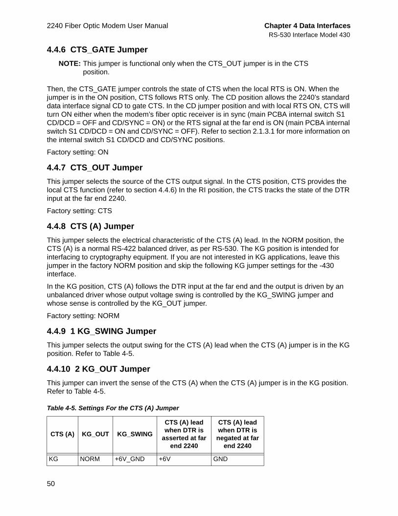
2240 Fiber Optic Modem User Manual Chapter 4 Data InterfacesRS-530 Interface Model 430
50
4.4.6 CTS_GATE JumperNOTE: This jumper is functional only when the CTS_OUT jumper is in the CTS
position.
Then, the CTS_GATE jumper controls the state of CTS when the local RTS is ON. When the jumper is in the ON position, CTS follows RTS only. The CD position allows the 2240’s standard data interface signal CD to gate CTS. In the CD jumper position and with local RTS ON, CTS will turn ON either when the modem’s fiber optic receiver is in sync (main PCBA internal switch S1 CD/DCD = OFF and CD/SYNC = ON) or the RTS signal at the far end is ON (main PCBA internal switch S1 CD/DCD = ON and CD/SYNC = OFF). Refer to section 2.1.3.1 for more information on the internal switch S1 CD/DCD and CD/SYNC positions.
Factory setting: ON
4.4.7 CTS_OUT JumperThis jumper selects the source of the CTS output signal. In the CTS position, CTS provides the local CTS function (refer to section 4.4.6) In the RI position, the CTS tracks the state of the DTR input at the far end 2240.
Factory setting: CTS
4.4.8 CTS (A) JumperThis jumper selects the electrical characteristic of the CTS (A) lead. In the NORM position, the CTS (A) is a normal RS-422 balanced driver, as per RS-530. The KG position is intended for interfacing to cryptography equipment. If you are not interested in KG applications, leave this jumper in the factory NORM position and skip the following KG jumper settings for the -430 interface.
In the KG position, CTS (A) follows the DTR input at the far end and the output is driven by an unbalanced driver whose output voltage swing is controlled by the KG_SWING jumper and whose sense is controlled by the KG_OUT jumper.
Factory setting: NORM
4.4.9 1 KG_SWING JumperThis jumper selects the output swing for the CTS (A) lead when the CTS (A) jumper is in the KG position. Refer to Table 4-5.
4.4.10 2 KG_OUT JumperThis jumper can invert the sense of the CTS (A) when the CTS (A) jumper is in the KG position. Refer to Table 4-5.
Table 4-5. Settings For the CTS (A) Jumper
CTS (A) KG_OUT KG_SWING
CTS (A) lead when DTR is
asserted at far end 2240
CTS (A) lead when DTR is negated at far
end 2240
KG NORM +6V_GND +6V GND
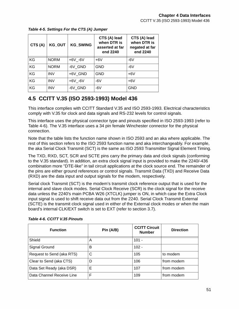
Chapter 4 Data InterfacesCCITT V.35 (ISO 2593-1993) Model 436
51
4.5 CCITT V.35 (ISO 2593-1993) Model 436This interface complies with CCITT Standard V.35 and ISO 2593-1993. Electrical characteristics comply with V.35 for clock and data signals and RS-232 levels for control signals.
This interface uses the physical connector type and pinouts specified in ISO 2593-1993 (refer to Table 4-6). The V.35 interface uses a 34 pin female Winchester connector for the physical connection.
Note that the table lists the function name shown in ISO 2593 and an aka where applicable. The rest of this section refers to the ISO 2593 function name and aka interchangeably. For example, the aka Serial Clock Transmit (SCT) is the same as ISO 2593 Transmitter Signal Element Timing.
The TXD, RXD, SCT, SCR and SCTE pins carry the primary data and clock signals (conforming to the V.35 standard). In addition, an extra clock signal input is provided to make the 2240/-436 combination more "DTE-like" in tail circuit applications at the clock source end. The remainder of the pins are either ground references or control signals. Transmit Data (TXD) and Receive Data (RXD) are the data input and output signals for the modem, respectively.
Serial clock Transmit (SCT) is the modem’s transmit clock reference output that is used for the internal and slave clock modes. Serial Clock Receive (SCR) is the clock signal for the receive data unless the 2240's main PCBA W26 (XTCLK) jumper is ON, in which case the Extra Clock input signal is used to shift receive data out from the 2240. Serial Clock Transmit External (SCTE) is the transmit clock signal used in either of the External clock modes or when the main board’s internal CLK/EXT switch is set to EXT (refer to section 3.7).
KG NORM +6V_-6V +6V -6V
KG NORM -6V_GND GND -6V
KG INV +6V_GND GND +6V
KG INV +6V_-6V -6V +6V
KG INV -6V_GND -6V GND
Table 4-6. CCITT V.35 Pinouts
Function Pin (A/B) CCITT Circuit Number Direction
Shield A 101 -
Signal Ground B 102 -
Request to Send (aka RTS) C 105 to modem
Clear to Send (aka CTS) D 106 from modem
Data Set Ready (aka DSR) E 107 from modem
Data Channel Receive Line F 109 from modem
Table 4-5. Settings For the CTS (A) Jumper
CTS (A) KG_OUT KG_SWING
CTS (A) lead when DTR is
asserted at far end 2240
CTS (A) lead when DTR is negated at far
end 2240
2240 Fiber Optic Modem User Manual Chapter 4 Data InterfacesCCITT V.35 (ISO 2593-1993) Model 436
52
NOTE: The previous V.35 interface, Model -435, did not conform to the ISO 2593 pinout and was the predecessor to the -436 interface. The signals listed in Table 4-7 have different pinouts on the -435 versus the -436. The -435 also did not support the Extra Clock for the receive data signal. This pinout difference table is only included as a reference.
Signal Detector (aka DCD)
Data Terminal Ready (aka DTR) H 108 to modem
Calling Indicator (aka RI) J 125 from modem
Local Loopback L 141 to modem
Remote Loopback N 140 to modem
Received Data (aka RXD) R/T 104 from modem
Receiver Signal Element V/X 115 from modem
Timing DCE Source (also known as SCR)
Transmitted Data (aka TXD) P/S 103 to modem
Transmitter Signal Element Y/AA 114 from modem
Timing DCE Source (aka SCT)
Transmitter Signal Element U/W 113 to modem
Timing DTE Source (aka SCTE)
Test Indicator (aka TM) NN 142 from modem
Secondary Transmit Data (aka STD)
K* - to modem
Secondary Receive Data (aka SRD)
M* - from modem
Extra Clock for Receive Data FF/DD* - to modem
NOTE 1: The 2240 connects the Shield pin to chassis ground.* These pins carry signals which are not defined by V.35 or ISO 2593-1993. If a straight-through cable is used, verify compatibility of this pin usage with the customer's equipment.
Table 4-7. Pinout Differences (-435 vs. -436)
Function Pin (A/B) CCITT Circuit Number Direction
Test Indicator C C 142 from modem
Secondary Receive Data L 119 from modem
Local Loopback E E 141 to modem
Table 4-6. CCITT V.35 Pinouts (Continued)
Function Pin (A/B) CCITT Circuit Number Direction
Chapter 4 Data InterfacesCCITT V.35 (ISO 2593-1993) Model 436
53
None of the control leads interact with the data transmission. They are provided in order to comply with a variety of DTE interface requirements. Most of the control leads are actually end-to-end signal channels which can be used for any purpose as long as it conforms to the V.35 interface standards.
The RTS, CTS and DCD pins function together to provide the most common handshake functions. An input to RTS (see description of RTS-Bias jumper) is transmitted to the DCD output at the other end of the link (see description of DCD jumper). CTS follows RTS locally but it is delayed by approximately 1 msec when RTS turns on (see description of CTS-Gate jumper). There are two other end-to-end control lead pairs. They are listed below with the input signal listed first:
• DTR to RI
• STD to SRD
Data Set Ready (DSR) typically indicates that the modem is ready to handle transmit data. During loopbacks, the behavior of this signal is dependent on the position of the DSR jumper (see description of DSR jumper). Test Mode (TM) is turned ON (asserted) ONLY when a loopback is active on either one or both modems.
Local Loopback (LL) and Remote Loopback (RL) are loopback control leads and perform the same functions as the 2240 front panel LOOP switch, LOC and REM positions. LL and RL are interface signal inputs which can be used to activate the LOC or REM loop functions. These signals can control the loopback functions only if the front panel switch is in the center or OFF position.
4.5.1 RTS_BIAS JumperThe RTS_BIAS jumper controls the state that RTS floats to when there is no signal driving the RTS pin. The OFF position forces this signal to the OFF (negated) state when the interface cable is disconnected. The ON position forces it to ON (asserted).
Factory Setting= OFF
4.5.2 DCD JumperThe DCD jumper determines the source of the DCD output. In the CTRL position, the DCD output functions as the output for the RTS input at the far end. In the CD jumper position and with local RTS ON, CTS will turn ON either when the modem’s fiber optic receiver is in sync (main PCBA internal switch S1 CD/DCD = OFF and CD/SYNC = ON) or the state of the RTS signal at the far end (main PCBA internal switch S1 CD/DCD = ON and CD/SYNC = OFF). Refer to section 2.1.3.1 for more information on the internal switch S1 CD/DCD and CD/SYNC positions.
Factory setting: CTRL
Remote Loopback D D 140 to modem
Table 4-7. Pinout Differences (-435 vs. -436)
Function Pin (A/B) CCITT Circuit Number Direction
2240 Fiber Optic Modem User Manual Chapter 4 Data InterfacesMulti-Channel Interfaces
54
4.5.3 CTS_GATE JumperThe CTS_GATE jumper controls the state of CTS when the local RTS is ON. When the jumper is in the ON position, CTS follows RTS only. The CD position allows the 2240’s standard data interface signal CD to gate CTS. In the CD jumper position and with local RTS ON, CTS will turn ON either when the modem’s fiber optic receiver is in sync (main PCBA internal switch S1 CD/DCD = OFF and CD/SYNC = ON) or the RTS signal at the far end is ON (main PCBA internal switch S1 CD/DCD = ON and CD/SYNC = OFF). Refer to section 2.1.3.1 for more information on the internal switch S1 CD/DCD and CD/SYNC positions.
Factory setting: ON
4.5.4 DSR JumperThe DSR jumper controls the behavior of the DSR signal. The CCITT turns DSR OFF when the far-end 2240 modem has a local loopback active. The TEST position causes DSR to turn OFF (negate) whenever any loopback is active at one or both modems.
Factory setting: CCITT
4.5.5 CH_GND JumperThe jumper selects whether chassis ground is connected directly to signal ground (SHORT position) or through a 100 Ohm resistor (100_OHM position).
NOTE: In the standalone model, the 100_OHM position will only put a 100 Ohm resistor between the two grounds if the 2240's main board SIGNAL GND jumper is set to the FLOAT position. When installed in the 2201 Rack Chassis, any modem main board, interface or rack chassis jumper being set to SHORT will override the FLOAT and 100_OHM positions on all of the other modems. CONSIDER THIS JUMPER CAREFULLY.
Factory setting: 100_OHM
4.6 Multi-Channel Interfaces
4.6.1 RS-449/RS-423 Model MC1This interface includes two physical connectors. The RS-449/422 uses a 37-pin, female D-Type connector and the RS-423 uses a 25-pin, female D-Type connector.
A typical application for this interface is to transport data and dialer information from a video location to the network equipment over fiber optic cable. The RS-449 interface can carry the Video Codec data with the control lead used for call set up. The RS-423 interface can carry either serial RS-232 data or parallel RS-366A data for the dialing equipment, when used with the appropriate RS-366A adapter (2240-366-ACE or 2240-366-DTE) or equivalent cables.
Table 4-8 delineates the adapter wiring necessary to utilize the RS-423 for both the DTE (Data Terminal Equipment) and ACE (Automatic Calling Equipment) ends.
Chapter 4 Data InterfacesMulti-Channel Interfaces
55
Table 4-8. RS-366A Adapters
4.6.2 RS-449/422 InterfaceThis interface complies with EIA Standard RS-449. Electrical characteristics comply with RS-422 for clock and data signals and RS-423 for control signals. The interface uses the physical connector type and pinouts specified in RS-449 (refer to Table 4-9). The RS-449/422 interface uses a 37-pin, female D-Type connector for the physical connection.
Table 4-9. RS-449 Pinouts for Model MC1
Pin Number
A/B
RS-449 Pin Name (abbrev) (full name) Direction
1 SHLD shield -
4/22 SD send data to modem
5/23 ST send timing from modem
6/24 RD receive data from modem
7/25 RS request to send to modem
8/26 RT receive timing from modem
9/27 CS clear to send from modem
10 LL local loopback to modem
11/29 DM data mode from modem
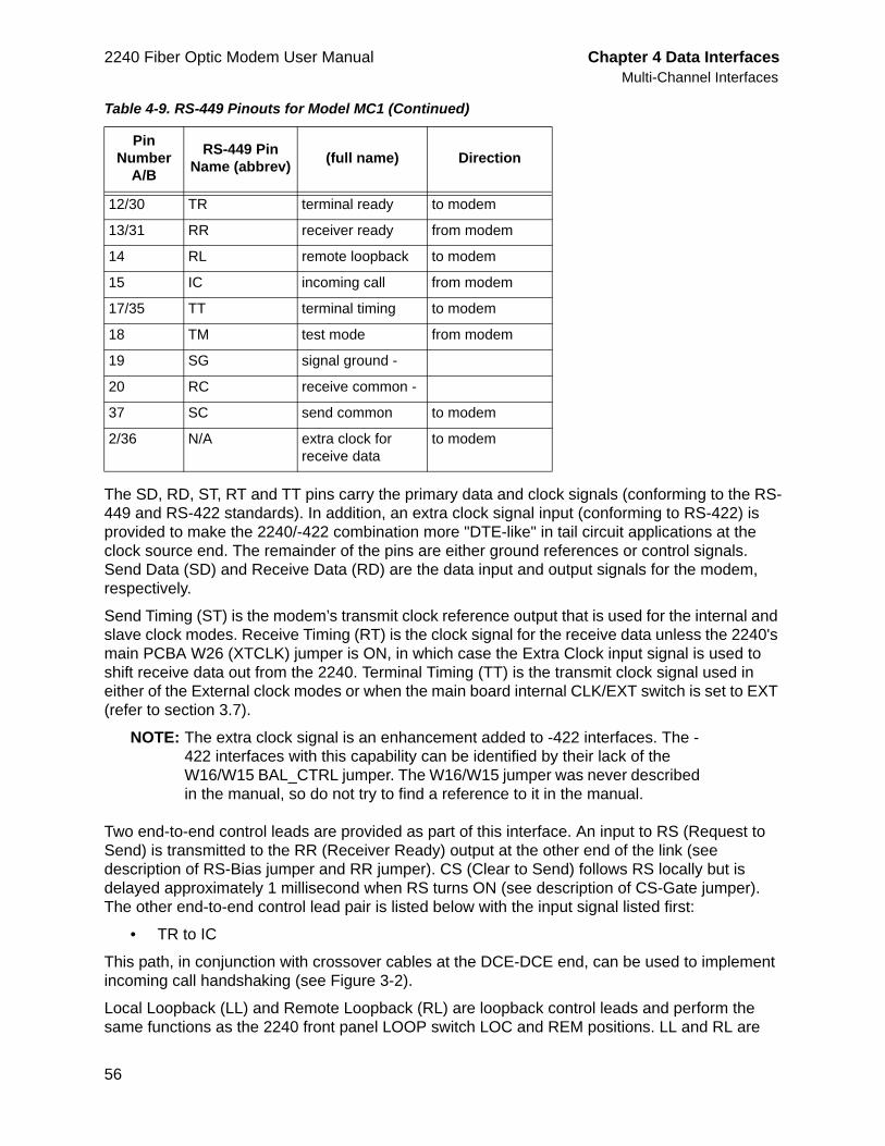
2240 Fiber Optic Modem User Manual Chapter 4 Data InterfacesMulti-Channel Interfaces
56
The SD, RD, ST, RT and TT pins carry the primary data and clock signals (conforming to the RS-449 and RS-422 standards). In addition, an extra clock signal input (conforming to RS-422) is provided to make the 2240/-422 combination more "DTE-like" in tail circuit applications at the clock source end. The remainder of the pins are either ground references or control signals. Send Data (SD) and Receive Data (RD) are the data input and output signals for the modem, respectively.
Send Timing (ST) is the modem’s transmit clock reference output that is used for the internal and slave clock modes. Receive Timing (RT) is the clock signal for the receive data unless the 2240's main PCBA W26 (XTCLK) jumper is ON, in which case the Extra Clock input signal is used to shift receive data out from the 2240. Terminal Timing (TT) is the transmit clock signal used in either of the External clock modes or when the main board internal CLK/EXT switch is set to EXT (refer to section 3.7).
NOTE: The extra clock signal is an enhancement added to -422 interfaces. The -422 interfaces with this capability can be identified by their lack of the W16/W15 BAL_CTRL jumper. The W16/W15 jumper was never described in the manual, so do not try to find a reference to it in the manual.
Two end-to-end control leads are provided as part of this interface. An input to RS (Request to Send) is transmitted to the RR (Receiver Ready) output at the other end of the link (see description of RS-Bias jumper and RR jumper). CS (Clear to Send) follows RS locally but is delayed approximately 1 millisecond when RS turns ON (see description of CS-Gate jumper). The other end-to-end control lead pair is listed below with the input signal listed first:
• TR to IC
This path, in conjunction with crossover cables at the DCE-DCE end, can be used to implement incoming call handshaking (see Figure 3-2).
Local Loopback (LL) and Remote Loopback (RL) are loopback control leads and perform the same functions as the 2240 front panel LOOP switch LOC and REM positions. LL and RL are
12/30 TR terminal ready to modem
13/31 RR receiver ready from modem
14 RL remote loopback to modem
15 IC incoming call from modem
17/35 TT terminal timing to modem
18 TM test mode from modem
19 SG signal ground -
20 RC receive common -
37 SC send common to modem
2/36 N/A extra clock for receive data
to modem
Table 4-9. RS-449 Pinouts for Model MC1 (Continued)
Pin Number
A/B
RS-449 Pin Name (abbrev) (full name) Direction
Chapter 4 Data InterfacesMulti-Channel Interfaces
57
interface signal inputs which can be used to activate the LOC or REM loop functions. These signals can control the loopback functions only if the front panel switch is in the center or OFF position.
4.6.3 RS_BIAS JumperThe RS_BIAS jumper controls the state that RS floats to when there is no signal driving the RS pin. The OFF position forces this signal to the OFF (negated) state when the interface cable is disconnected. The ON position forces it to ON (asserted).
Factory setting: OFF
4.6.4 RR JumperThe RR jumper determines the source of the RR output. In the CTRL position, the RR output functions as the output for the RS input at the far end. In the CD jumper position, the RR output will turn ON either when the modem's fiber optic receiver is in sync (main PCBA internal switch S1 CD/DCD = OFF and CD/SYNC = ON) or when the far end RTS is ON (main PCBA 8internal switch S1 CD/DCD = ON and CD/SYNC = OFF). Refer to section 2.1.3.1 for more information on the internal switch S1 CD/DCD and CD/SYNC positions.
Factory setting: CTRL
4.6.5 CS_GATE JumperThe CS_GATE jumper controls the state of CS when the local RS is ON. When the jumper is in the ON position, CTS follows RS only. The CD position allows the 2240's standard data interface signal CD to gate CS. In the CD jumper position and with local RS ON, CS will turn ON either when the modem's fiber optic receiver is in sync (main board internal switch S1 CD/DCD = OFF and CD/SYNC = ON) or the RTS signal at the far end is ON (main board internal switch S1 CD/DCD = ON and CD/SYNC = OFF). Refer to section 2.1.3.1 for more information on the internal switch S1 CD/DCD and CD/SYNC positions.
Factory setting: ON
4.6.6 CH_GND JumperThe jumper selects whether chassis ground is connected directly to signal ground (SHORT position) or through a 100 Ohm resistor (100_OHM position).
NOTE: In the standalone model, the 100_OHM position will only put a 100 Ohm resistor between the two grounds if the 2240's main board SIGNAL GND jumper is set to the FLOAT position.
When installed in the 2201 Rack Chassis, any modem main board, interface or rack chassis jumper being set to SHORT will override the FLOAT and 100_OHM positions on all of the other modems. CONSIDER THIS JUMPER CAREFULLY.
Factory setting: 100_OHM
4.6.7 UNBAL_REF JumperRS-449 specifies that unbalanced inputs to a DCE are to be referenced to the SC (Send Common) pin. This pin on the DCE is tied to the signal ground of the DTE through the interface
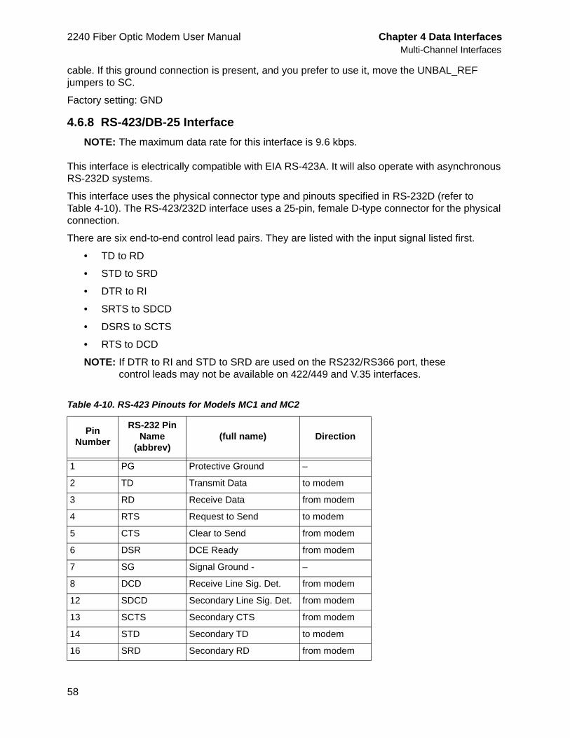
2240 Fiber Optic Modem User Manual Chapter 4 Data InterfacesMulti-Channel Interfaces
58
cable. If this ground connection is present, and you prefer to use it, move the UNBAL_REF jumpers to SC.
Factory setting: GND
4.6.8 RS-423/DB-25 InterfaceNOTE: The maximum data rate for this interface is 9.6 kbps.
This interface is electrically compatible with EIA RS-423A. It will also operate with asynchronous RS-232D systems.
This interface uses the physical connector type and pinouts specified in RS-232D (refer to Table 4-10). The RS-423/232D interface uses a 25-pin, female D-type connector for the physical connection.
There are six end-to-end control lead pairs. They are listed with the input signal listed first.
• TD to RD
• STD to SRD
• DTR to RI
• SRTS to SDCD
• DSRS to SCTS
• RTS to DCD
NOTE: If DTR to RI and STD to SRD are used on the RS232/RS366 port, these control leads may not be available on 422/449 and V.35 interfaces.
Table 4-10. RS-423 Pinouts for Models MC1 and MC2
Pin Number
RS-232 Pin Name
(abbrev)(full name) Direction
1 PG Protective Ground –
2 TD Transmit Data to modem
3 RD Receive Data from modem
4 RTS Request to Send to modem
5 CTS Clear to Send from modem
6 DSR DCE Ready from modem
7 SG Signal Ground - –
8 DCD Receive Line Sig. Det. from modem
12 SDCD Secondary Line Sig. Det. from modem
13 SCTS Secondary CTS from modem
14 STD Secondary TD to modem
16 SRD Secondary RD from modem
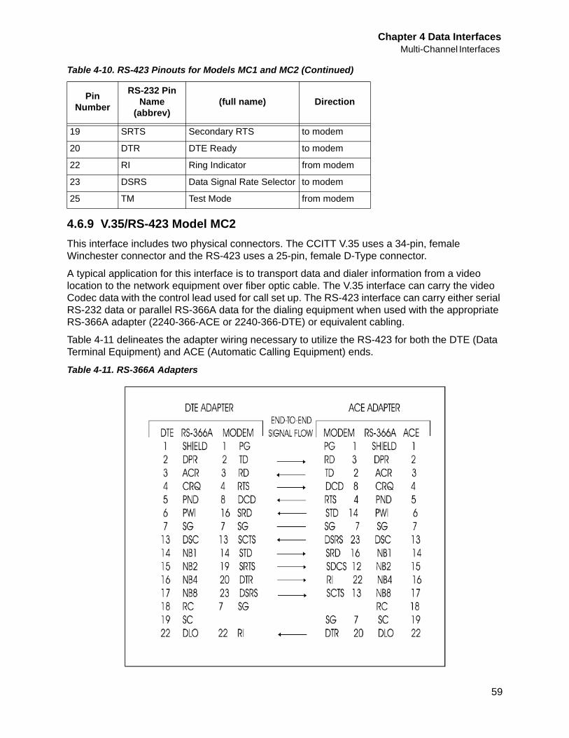
Chapter 4 Data InterfacesMulti-Channel Interfaces
59
4.6.9 V.35/RS-423 Model MC2This interface includes two physical connectors. The CCITT V.35 uses a 34-pin, female Winchester connector and the RS-423 uses a 25-pin, female D-Type connector.
A typical application for this interface is to transport data and dialer information from a video location to the network equipment over fiber optic cable. The V.35 interface can carry the video Codec data with the control lead used for call set up. The RS-423 interface can carry either serial RS-232 data or parallel RS-366A data for the dialing equipment when used with the appropriate RS-366A adapter (2240-366-ACE or 2240-366-DTE) or equivalent cabling.
Table 4-11 delineates the adapter wiring necessary to utilize the RS-423 for both the DTE (Data Terminal Equipment) and ACE (Automatic Calling Equipment) ends.
Table 4-11. RS-366A Adapters
19 SRTS Secondary RTS to modem
20 DTR DTE Ready to modem
22 RI Ring Indicator from modem
23 DSRS Data Signal Rate Selector to modem
25 TM Test Mode from modem
Table 4-10. RS-423 Pinouts for Models MC1 and MC2 (Continued)
Pin Number
RS-232 Pin Name
(abbrev)(full name) Direction
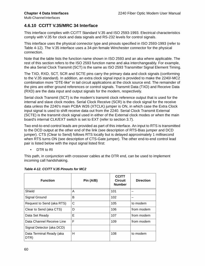
Chapter 4 Data Interfaces 2240 Fiber Optic Modem User ManualMulti-Channel Interfaces
60
4.6.10 CCITT V.35/MRC 34 InterfaceThis interface complies with CCITT Standard V.35 and ISO 2593-1993. Electrical characteristics comply with V.35 for clock and data signals and RS-232 levels for control signals.
This interface uses the physical connector type and pinouts specified in ISO 2593-1993 (refer to Table 4-12). The V.35 interface uses a 34-pin female Winchester connector for the physical connection.
Note that the table lists the function name shown in ISO 2593 and an aka where applicable. The rest of this section refers to the ISO 2593 function name and aka interchangeably. For example, the aka Serial Clock Transmit (SCT) is the same as ISO 2593 Transmitter Signal Element Timing.
The TXD, RXD, SCT, SCR and SCTE pins carry the primary data and clock signals (conforming to the V.35 standard). In addition, an extra clock signal input is provided to make the 2240/-MC2 combination more "DTE-like" in tail circuit applications at the clock source end. The remainder of the pins are either ground references or control signals. Transmit Data (TXD) and Receive Data (RXD) are the data input and output signals for the modem, respectively.
Serial clock Transmit (SCT) is the modem’s transmit clock reference output that is used for the internal and slave clock modes. Serial Clock Receive (SCR) is the clock signal for the receive data unless the 2240's main PCBA W26 (XTCLK) jumper is ON, in which case the Extra Clock input signal is used to shift receive data out from the 2240. Serial Clock Transmit External (SCTE) is the transmit clock signal used in either of the External clock modes or when the main board's internal CLK/EXT switch is set to EXT (refer to section 3.7).
Two end-to-end control leads are provided as part of this interface. An input to RTS is transmitted to the DCD output at the other end of the link (see description of RTS-Bias jumper and DCD jumper). CTS (Clear to Send) follows RTS locally but is delayed approximately 1 millisecond when RTS turns ON (see description of CTS-Gate jumper). The other end-to-end control lead pair is listed below with the input signal listed first:
• DTR to RI
This path, in conjunction with crossover cables at the DTR end, can be used to implement incoming call handshaking.
Table 4-12. CCITT V.35 Pinouts for MC2
Function Pin (A/B)CCITT Circuit
NumberDirection
Shield A 101 –
Signal Ground B 102 –
Request to Send (aka RTS) C 105 to modem
Clear to Send (aka CTS) D 106 from modem
Data Set Ready E 107 from modem
Data Channel Receive Line F 109 from modem
Signal Detector (aka DCD)
Data Terminal Ready (aka DTR)
H 108 to modem
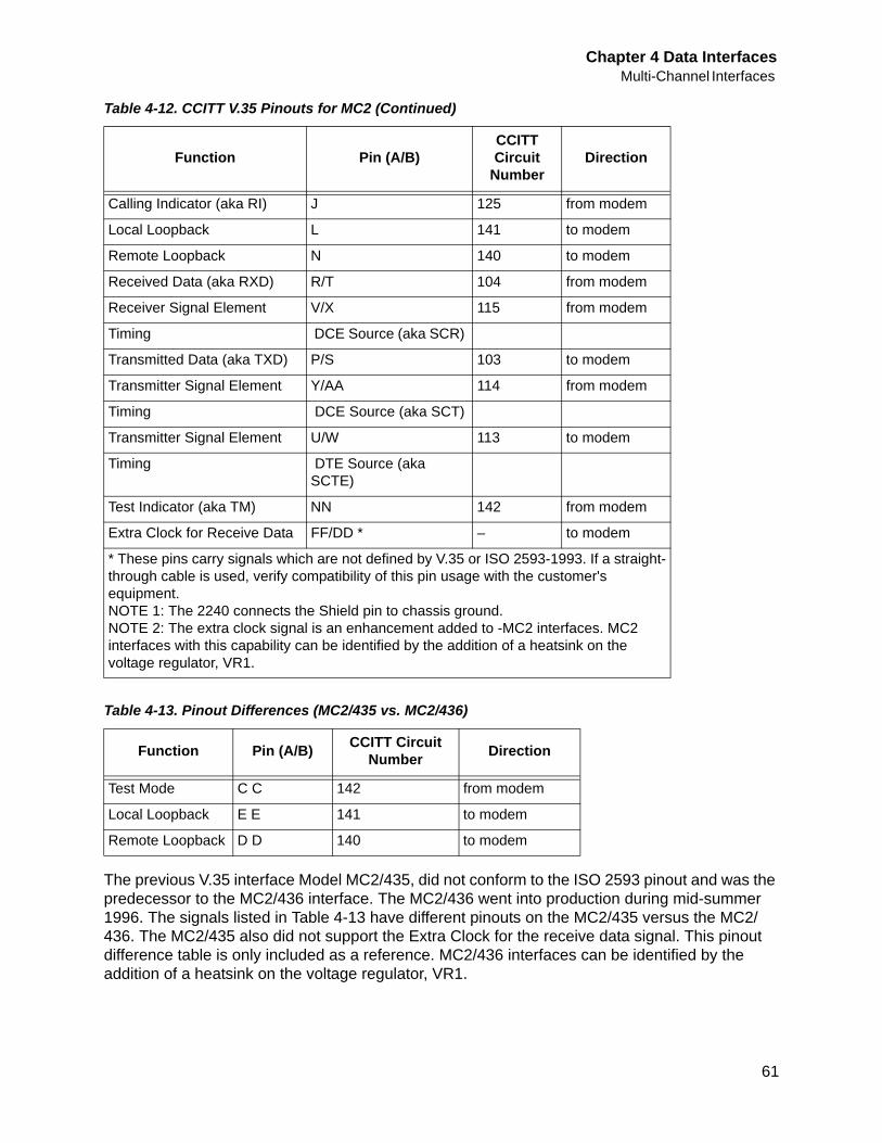
Chapter 4 Data InterfacesMulti-Channel Interfaces
61
The previous V.35 interface Model MC2/435, did not conform to the ISO 2593 pinout and was the predecessor to the MC2/436 interface. The MC2/436 went into production during mid-summer 1996. The signals listed in Table 4-13 have different pinouts on the MC2/435 versus the MC2/436. The MC2/435 also did not support the Extra Clock for the receive data signal. This pinout difference table is only included as a reference. MC2/436 interfaces can be identified by the addition of a heatsink on the voltage regulator, VR1.
Calling Indicator (aka RI) J 125 from modem
Local Loopback L 141 to modem
Remote Loopback N 140 to modem
Received Data (aka RXD) R/T 104 from modem
Receiver Signal Element V/X 115 from modem
Timing DCE Source (aka SCR)
Transmitted Data (aka TXD) P/S 103 to modem
Transmitter Signal Element Y/AA 114 from modem
Timing DCE Source (aka SCT)
Transmitter Signal Element U/W 113 to modem
Timing DTE Source (aka SCTE)
Test Indicator (aka TM) NN 142 from modem
Extra Clock for Receive Data FF/DD * – to modem
* These pins carry signals which are not defined by V.35 or ISO 2593-1993. If a straight-through cable is used, verify compatibility of this pin usage with the customer's equipment.NOTE 1: The 2240 connects the Shield pin to chassis ground.NOTE 2: The extra clock signal is an enhancement added to -MC2 interfaces. MC2 interfaces with this capability can be identified by the addition of a heatsink on the voltage regulator, VR1.
Table 4-13. Pinout Differences (MC2/435 vs. MC2/436)
Function Pin (A/B) CCITT Circuit Number Direction
Test Mode C C 142 from modem
Local Loopback E E 141 to modem
Remote Loopback D D 140 to modem
Table 4-12. CCITT V.35 Pinouts for MC2 (Continued)
Function Pin (A/B)CCITT Circuit
NumberDirection
Chapter 4 Data Interfaces 2240 Fiber Optic Modem User ManualMulti-Channel Interfaces
62
4.6.11 RTS_BIAS JumperThe RTS_BIAS jumper controls the state that RTS floats to when there is no signal driving the RTS pin. The OFF position forces this signal to the OFF (negated) state when the interface cable is disconnected. The ON position forces it to ON (asserted).
Factory setting: OFF
4.6.12 DCD JumperThe DCD jumper determines the source of the DCD output. In the CTRL position, the DCD output functions as the output for the RTS input at the far end. In the CD jumper position and with local RTS ON, CTS will turn ON either when the modem’s fiber optic receiver is in sync (main PCBA internal switch S1 CD/DCD = OFF and CD/SYNC = ON) or the state of the RTS signal at the far end (main PCBA internal switch S1 CD/DCD = ON and CD/SYNC = OFF). Refer to section 2.1.3.1 for more information on the internal switch S1 CD/DCD and CD/SYNC positions.
Factory setting: CTRL
4.6.13 CTS_GATE JumperThe CTS_GATE jumper controls the state of CTS when the local RTS is ON. When the jumper is in the ON position, CTS follows RTS only. The CD position allows the 2240's standard data interface signal CD to gate CTS. In the CD jumper position and with local RTS ON, CTS will turn ON either when the modem’s fiber optic receiver is in sync (main PCBA internal switch S1 CD/DCD = OFF and CD/SYNC = ON) or the RTS signal at the far end is ON (main PCBA internal switch S1 CD/DCD = ON and CD/SYNC = OFF). Refer to section 2.1.3.1 for more information on the internal switch S1 CD/DCD and CD/SYNC positions.
Factory setting: ON
4.6.14 CH_GND JumperThe jumper selects whether chassis ground is connected directly to signal ground (SHORT position) or through a 100 Ohm resistor (100_OHM position).
NOTE: In the standalone model, the 100_OHM position will only put a 100 Ohm resistor between the two grounds if the 2240's main board SIGNAL GND jumper is set to the FLOAT position. When installed in the 2201 Rack Chassis, any modem main board, interface or rack chassis jumper being set to SHORT will override the FLOAT and 100_OHM positions on all of the other modems. CONSIDER THIS JUMPER CAREFULLY.
Factory setting: 100_OHM
4.6.15 RS-423/DB-25 InterfaceNOTE: The maximum data rate for this interface is 9.6 Kbps.
This interface is electrically compatible with EIA RS-423A. It will also operate with asynchronous RS-232D systems.
This interface uses the physical connector type and pinouts specified in RS-232D (refer to Table 4-10). The RS-423/232D interface uses a 25-pin, female D-type connector for the physical
Chapter 4 Data InterfacesT1/E1 Interfaces
63
connection. These signal channels operate independently from the main data channel of the V.35 interface. A worst case sampling jitter of 21 microseconds will be experienced on these channels.
There are six end-to-end control lead pairs. They are listed below with the input signal listed first:
• TD to RD
• STD to SzRD
• DTR to RI
• SRTS to SDCD
• DSRS to SCTS
• RTS to DCD
4.7 T1/E1 Interfaces
4.7.1 Transparent Bipolar - Models 4BXNOTE: This interface replaces the 4T (1-3) and 4E (1-3) models. It is completely
compatible with these previous interface models.
The 4Bx interfaces are compatible with any bipolar, line-coded T1 or E1 data (1.544 or 2.048 Mbps). All types of codes, including AMI, B8ZS, B7S or HDB3, will be accurately transmitted/received. Five DIP switches are used in configuring particular applications (refer to Table 4-14). Switch positions 1 and 2 select T1 or E1. Positions 3 through 5 select line build out values for T1 usage.
There are three different types of interface connectors, and each is identified by the number at the end of the interface code of the order number (refer to Table 4-15). The connectors are female DA-15 (4B1); four-position terminal block (4B2); or two female BNCs (4B3). Figure 4-2 shows how the input and output pairs are wired to these connectors.
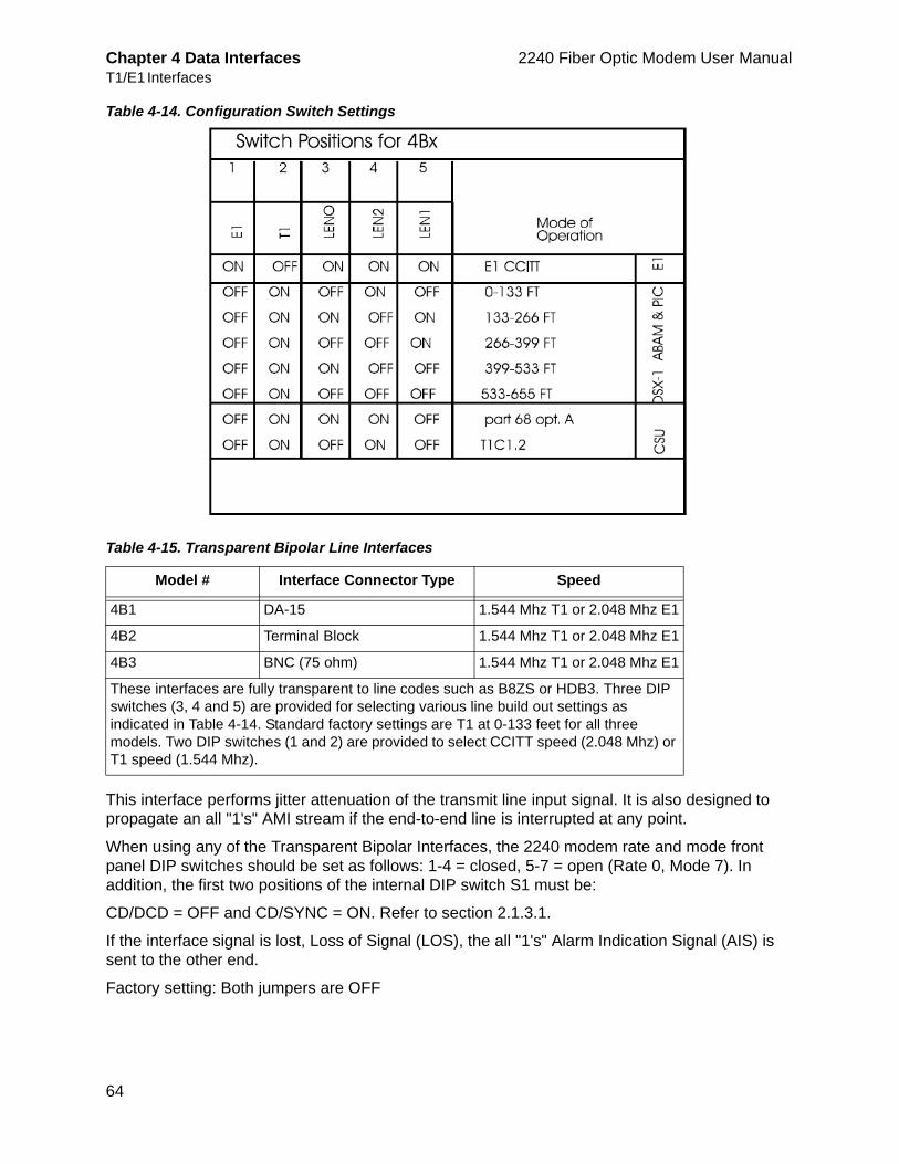
Chapter 4 Data Interfaces 2240 Fiber Optic Modem User ManualT1/E1 Interfaces
64
Table 4-14. Configuration Switch Settings
This interface performs jitter attenuation of the transmit line input signal. It is also designed to propagate an all "1's" AMI stream if the end-to-end line is interrupted at any point.
When using any of the Transparent Bipolar Interfaces, the 2240 modem rate and mode front panel DIP switches should be set as follows: 1-4 = closed, 5-7 = open (Rate 0, Mode 7). In addition, the first two positions of the internal DIP switch S1 must be:
CD/DCD = OFF and CD/SYNC = ON. Refer to section 2.1.3.1.
If the interface signal is lost, Loss of Signal (LOS), the all "1's" Alarm Indication Signal (AIS) is sent to the other end.
Factory setting: Both jumpers are OFF
Table 4-15. Transparent Bipolar Line Interfaces
Model # Interface Connector Type Speed
4B1 DA-15 1.544 Mhz T1 or 2.048 Mhz E1
4B2 Terminal Block 1.544 Mhz T1 or 2.048 Mhz E1
4B3 BNC (75 ohm) 1.544 Mhz T1 or 2.048 Mhz E1
These interfaces are fully transparent to line codes such as B8ZS or HDB3. Three DIP switches (3, 4 and 5) are provided for selecting various line build out settings as indicated in Table 4-14. Standard factory settings are T1 at 0-133 feet for all three models. Two DIP switches (1 and 2) are provided to select CCITT speed (2.048 Mhz) or T1 speed (1.544 Mhz).
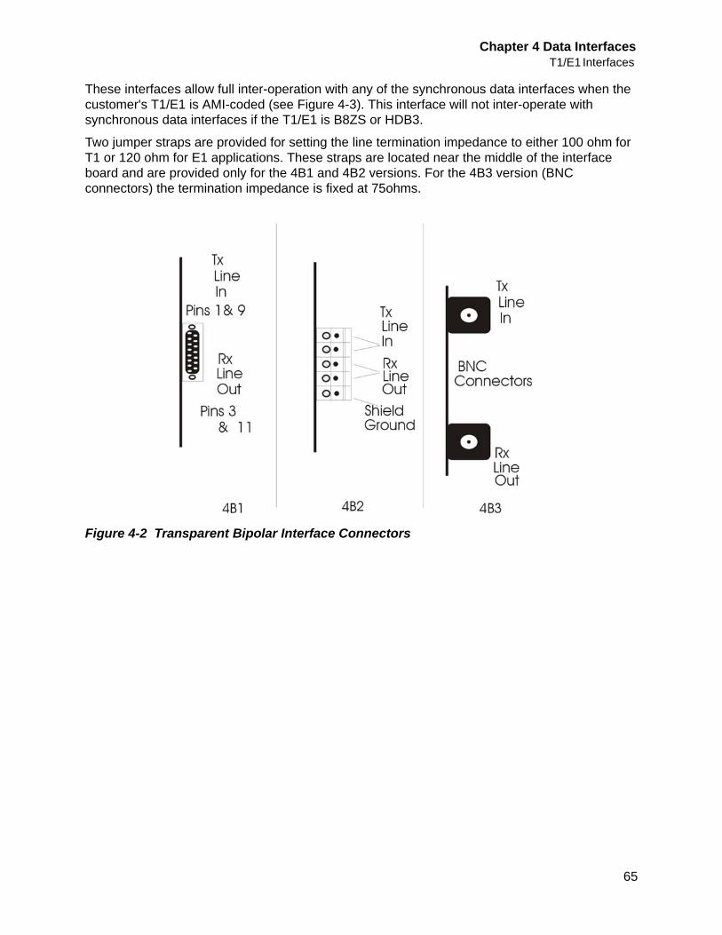
Chapter 4 Data InterfacesT1/E1 Interfaces
65
These interfaces allow full inter-operation with any of the synchronous data interfaces when the customer's T1/E1 is AMI-coded (see Figure 4-3). This interface will not inter-operate with synchronous data interfaces if the T1/E1 is B8ZS or HDB3.
Two jumper straps are provided for setting the line termination impedance to either 100 ohm for T1 or 120 ohm for E1 applications. These straps are located near the middle of the interface board and are provided only for the 4B1 and 4B2 versions. For the 4B3 version (BNC connectors) the termination impedance is fixed at 75ohms.
Figure 4-2 Transparent Bipolar Interface Connectors
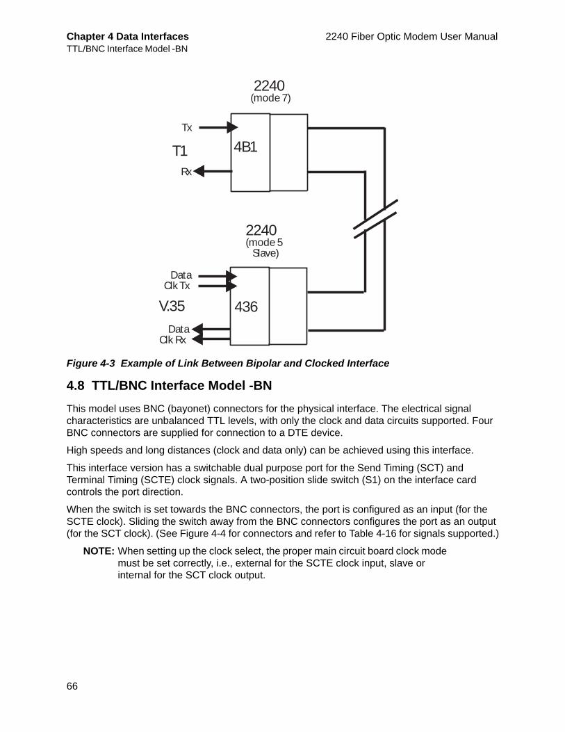
Chapter 4 Data Interfaces 2240 Fiber Optic Modem User ManualTTL/BNC Interface Model -BN
66
Figure 4-3 Example of Link Between Bipolar and Clocked Interface
4.8 TTL/BNC Interface Model -BNThis model uses BNC (bayonet) connectors for the physical interface. The electrical signal characteristics are unbalanced TTL levels, with only the clock and data circuits supported. Four BNC connectors are supplied for connection to a DTE device.
High speeds and long distances (clock and data only) can be achieved using this interface.
This interface version has a switchable dual purpose port for the Send Timing (SCT) and Terminal Timing (SCTE) clock signals. A two-position slide switch (S1) on the interface card controls the port direction.
When the switch is set towards the BNC connectors, the port is configured as an input (for the SCTE clock). Sliding the switch away from the BNC connectors configures the port as an output (for the SCT clock). (See Figure 4-4 for connectors and refer to Table 4-16 for signals supported.)
NOTE: When setting up the clock select, the proper main circuit board clock mode must be set correctly, i.e., external for the SCTE clock input, slave or internal for the SCT clock output.
T1
2240(mode 7)
2240(mode 5 Slave)
V.35
Rx
Tx
DataClk Tx
DataClk Rx
4B1
436
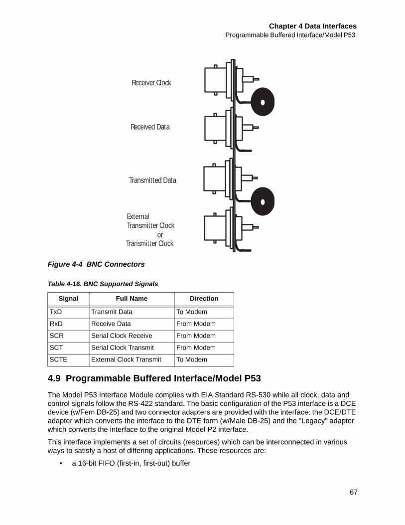
Chapter 4 Data InterfacesProgrammable Buffered Interface/Model P53
67
Figure 4-4 BNC Connectors
4.9 Programmable Buffered Interface/Model P53The Model P53 Interface Module complies with EIA Standard RS-530 while all clock, data and control signals follow the RS-422 standard. The basic configuration of the P53 interface is a DCE device (w/Fem DB-25) and two connector adapters are provided with the interface: the DCE/DTE adapter which converts the interface to the DTE form (w/Male DB-25) and the "Legacy" adapter which converts the interface to the original Model P2 interface.
This interface implements a set of circuits (resources) which can be interconnected in various ways to satisfy a host of differing applications. These resources are:
• a 16-bit FIFO (first-in, first-out) buffer
Table 4-16. BNC Supported Signals
Signal Full Name Direction
TxD Transmit Data To Modem
RxD Receive Data From Modem
SCR Serial Clock Receive From Modem
SCT Serial Clock Transmit From Modem
SCTE External Clock Transmit To Modem
Receiver Clock
Received Data
Transmitted Data
Transmitter Clock
ExternalTransmitter Clock
or
Chapter 4 Data Interfaces 2240 Fiber Optic Modem User ManualProgrammable Buffered Interface/Model P53
68
• an inverter
• a switchable delay line
The FIFO can be utilized to buffer either the received or the transmitted data (not both). The Delay Line, in conjunction with a four-position DIP switch, provides an option for fine tuning the relationship between clock and data timing. Table 4-17 defines the delay lines versus switch settings for the Model P53 Interface.
A wire wrap header (J3) provides the means to interconnect these resources together with the standard modem transmit and receive circuits to perform the intended function. Figure 4-5 illustrates how the resources are tied into the J3 header. Specific applications are satisfied by wire wrap connections between appropriate pins.
Four pre-wrapped headers are provided with the interface. These implement the most common applications. See the following figures: Figure 4-7, Figure 4-9, Figure 4-11, Figure 4-13. Numerous other configurations are possible by different wired versions of the header, P3. The four versions included are identified by part number labels affixed to the underside of the header. The version included in the socket as shipped is P/N 610030-001 (see Figure 4-13).
The P53 can be used to interface with encryption devices on the BLACK side where modems act as the network and supply clocking in a synchronous configuration, or to the RED (clear) side of a data encryption (KG) equipment. In the RED side application, the interface acts as the "tail-circuit adapter" device. This configuration allows the modem to accept two synchronous clocks (typically, DCE devices only accept one): one for transmit (external clock) and one for receive (FIFO input clock).
Another common application is with systems that communicate over geosynchronous satellites. In this application, the FIFO is used to make up for clock drift (Doppler shift) caused by the satellite's elliptical orbit around the earth.
Chapter 4 Data InterfacesProgrammable Buffered Interface/Model P53
69
Figure 4-5 Available Strapping Options for Programmable Buffered Interface
Chapter 4 Data Interfaces 2240 Fiber Optic Modem User ManualProgrammable Buffered Interface/Model P53
70
Figure 4-6 Board Layout for Programmable Buffered Interface
Table 4-17. Delay Times for Programmable Buffered Interface
SW1 Position(O)pen (C)losed Delay Time
P531 2 3 4
C C C C** 20 ns
O C C C 30 ns
C O C C 40 ns
O O C C 50 ns
C C O C 60 ns
O C O C 70 ns
C O O C 80 ns
O O O C 90 ns
C C C O 100 ns
O C C O 110 ns
C O C O 120 ns
O O C O 130 ns
C C O O 140 ns
O C O O 150 ns
C O O O 160 ns
O O O O 170 ns
** Default setting as shipped
W8 W9 W7
W14 W13 W12
-6V +/-6V+6V
100 ohmCHASSIS GND
W2W1SHORT
J3
RSTBIAS
OFF ON KG NORMW18 W17
W6
W5
W19 W20
Test GND
DSR
W16W15
Dl1 Sw1
W10
W11
INVERT
NORM
KG OUT
Chapter 4 Data InterfacesProgrammable Buffered Interface/Model P53
71
4.9.1 Jumper and Switch SettingsAll jumper settings and descriptions are listed in Table 4-18. This interface has strap option jumpers to configure the RLSD Output at J1-8 (DB-25) to support the KG-194 Resync capability. Jumper straps W10/W11 (adjacent to U11) and W12/W13/W14 (adjacent to U8) implement this function (refer to Table 4-18 and Figure 4-6). Jumper straps W10/W11 control the ON/OFF level and W12/W13/W14 configure the RLSD Output to Bipolar (+6 V and -6 V) or single-ended (+6 and 0 or -6 and 0).
The W1/W2 strap connects chassis ground to signal ground (W2 position), connects chassis ground through 100 ohms to signal ground (W1 position), or isolates chassis ground from signal ground (jumper out). The W5, W6 and W7 jumpers, when installed, ground the midpoints of the 100 ohm termination resistances of the FIFO CLK, SCTE and TxD line receivers. These jumpers may provide improved performance in cases where the RS-422 inputs are bipolar rather than the more common unipolar types. The W8, W9 and W15/W16 jumpers are used for converting to the Legacy configuration (see Figure 4-15).
Table 4-18. Jumper Settings and Descriptions
Jumper Description Notes Factory Setting
W1/W2 Chassis Ground W1 - 100 ohms/W2 - Short W1 Default
W5/W6/W7 RCVR Terminations All Out
W8/W9 Legacy Config. Both Out
W10/W11 RLSD Output Swing W11
W12/W13/W14 RLSD Output Swing W13
W15/W16 DSR W15 - Test/W16 - GND W16 Default
W17/W18 RTS Bias W17 - On/W18 - Off W18 Default
W19/W20 RLSD W19 - Single Ended/W20 - Differential
W20 Default
Table 4-19. Strap Configurations for RLSD (CD) Output
Strap Configurations CD Output (at J1-8**) Voltage Level ±1 V On/Off
W11 and W14 +6/-6
W11 and W12 +6/0
W11 and W13 0/-6
W10 and W14 -6/+6
W10 and W12 0/+6
W10 and W13 -6/0
** J1-6 when using the "Legacy" (P2) Converter
Chapter 4 Data Interfaces 2240 Fiber Optic Modem User ManualProgrammable Buffered Interface/Model P53
72
To support Flow Control, set the CD options at the Internal Option Switches on the main 2240 board. Set SW1-1, CD/DCD to ON. Set SW1-2, CD/SYNC, to OFF. For details about the switch, see section 2.1.3.
4.9.2 Generic InterfaceFigure 4-7 illustrates basic DCE configurations, which bypass all the "feature" circuits provided by the P53 Interface.
Chapter 4 Data InterfacesProgrammable Buffered Interface/Model P53
73
Programmable Buffered Interface Model P53, Generic DCE RS-530 P/N 6100030-006
Figure 4-7 Programmable Buffered Interface, Model P53, Basic DCE RS-530
KG SwingJumpers
InternalClock From
Modem
Rx Data
Tx Clock
Tx Data
ModemAlarm
Function
FromFiber
Circuits
ToFiber
Circuits
DelayLine
Inverter
FIFOData Out Data In
Shift Out Shift InW19
W208
FIFOClock
SCTE
TxDxD
From Modem
To Modem
To Modem
10 5
12
19
13
3
4
9
6
1
2
11
10
15
7
8
20
23
24
11
2
14
LL
RL
SCT
RLSD
RxD
SCR
IN
OUT
J1(D
B -
25)
7
1
CTS
SG
FG
DSR
RTS
5
13
22
19
18
21
6
4
P/N 6100030-006
Wire WrapNet List
6-137-178-189-19
14-15
3
16
17
9
15
1214
16
17
18
Chapter 4 Data Interfaces 2240 Fiber Optic Modem User ManualProgrammable Buffered Interface/Model P53
74
4.9.3 External StationThe External Station is used when an external station clock is providing timing (see Figure 4-8 and Figure 4-9). When connecting KG or KIV encryptors together on the Black side, using an external timing device you should install the external station clock strapped header in the J3 position. In this application, the modems are acting as the network, although the timing input is from an outside source. The modem in which the timing source is connected should be set for external and the other modem set for slave. This header is provided with the interface. The figures below show a typical external station clock application.
Figure 4-8 External Station Programmable Buffered Interface, Model P53, DCE RS-530
Figure 4-9 Programmable Buffered Interface, Model P53, External Station
CANOGACANOGAPERKINSPERKINS
DataData
RxRx TxTx
ClockClock
Rate modeRate mode
PwrPwrLoopLoop
OnOnRem/LocRem/Loc
22702270FiberFiber
ModemModem
OpticsOptics
TXTXRXRX
OffOff
CANOGACANOGAPERKINSPERKINS
DataData
RxRx TxTx
ClockClock
Rate modeRate mode
PwrPwrLoopLoop
OnOnRem/LocRem/Loc
22702270FiberFiber
ModemModem
OpticsOptics
TXTXRXRX
OffOff
MM or SMFiber Optics
KG/KIV
RED BLK
StationClock
KG/KIV
REDBLK
RxD
KG SwingJumpers
InternalClock From
Modem
Rx Data
Tx Clock
Tx Data
ModemAlarm
Function
FromFiber
Circuits
ToFiber
Circuits
DelayLine
Inverter
FIFOData Out Data In
Shift Out Shift InW19
W208
10
3
16
17
9
15
12
CTS
DSR
RTS
FIFOClock
SCTE
TxDxD
From Modem
To Modem
To Modem
5
12
19
13
14
16
17
18
3
4
9
6
1
2
11
10
15
7
8
20
23
24
11
2
14
LL
RL
SCT
RLSD
SCR
IN
OUT
J1(D
B -
25)
7 SG
1 FG
5
13
22
19
18
21
6
4
Wire WrapNet List
3-64-9
5-7, 14 & 178-18
12-19
P/N 6100030-004
Chapter 4 Data InterfacesProgrammable Buffered Interface/Model P53
75
4.9.4 InternalThe internal function is used when network equipment is set for Eternal Timing (see Figure 4-10 and Figure 4-11). When connecting KG or KIV encryptors together on the Black side, you should install the internal strapped header in the J3 position. In this application, the modems are acting as the network timing source. In most cases, both modems should be set for internal master clock. The rate switches should be set to the appropriate speed for the circuit. This header is provided with the interface. The figures below show a typical internal clock application.
Figure 4-10 Internal Programmable Buffered Interface, Model P53, DCE RS-530
Figure 4-11 Internal Programmable Buffered Interface, Model P53
CANOGACANOGAPERKINSPERKINS
DataData
RxRx TxTx
ClockClock
Rate modeRate mode
PwrPwrLoopLoop
OnOnRem/LocRem/Loc
22702270FiberFiber
ModemModem
OpticsOptics
TXTXRXRX
OffOff
CANOGACANOGAPERKINSPERKINS
DataData
RxRx TxTx
ClockClock
Rate modeRate mode
PwrPwrLoopLoop
OnOnRem/LocRem/Loc
22702270FiberFiber
ModemModem
OpticsOptics
TXTXRXRX
OffOff
MM or SMFiber Optics
KG/KIV
RED BLK
KG/KIV
REDBLK
RLSD
KG SwingJumpers
InternalClock From
Modem
Rx Data
Tx Clock
Tx Data
ModemAlarm
Function
FromFiber
Circuits
ToFiber
Circuits
DelayLine
Inverter
FIFOData Out Data In
Shift Out Shift InW19
W208
10
3
16
17
9
12
15
SG
FG
CTS
DSR
RTS
FIFOClock
SCTE
TxDxD
From Modem
To Modem
To Modem
5
12
19
13
14
16
17
18
3
4
9
6
1
2
11
10
15
7
8
20
23
24
11
2
14
LL
RL
SCT
RxD
SCR
IN
OUT
J1(D
B -
25)
7
1
5
13
22
19
18
21
6
4
P/N 6100030-005Wire Wrap
Net List6-137-178-189-19
10-1411-15
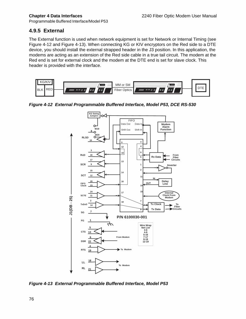
Chapter 4 Data Interfaces 2240 Fiber Optic Modem User ManualProgrammable Buffered Interface/Model P53
76
4.9.5 ExternalThe External function is used when network equipment is set for Network or Internal Timing (see Figure 4-12 and Figure 4-13). When connecting KG or KIV encryptors on the Red side to a DTE device, you should install the external strapped header in the J3 position. In this application, the modems are acting as an extension of the Red side cable in a true tail circuit. The modem at the Red end is set for external clock and the modem at the DTE end is set for slave clock. This header is provided with the interface.
Figure 4-12 External Programmable Buffered Interface, Model P53, DCE RS-530
Figure 4-13 External Programmable Buffered Interface, Model P53
CANOGACANOGAPERKINSPERKINS
DataData
RxRx TxTx
ClockClock
Rate modeRate mode
PwrPwrLoopLoop
OnOnRem/LocRem/Loc
22702270FiberFiber
ModemModem
OpticsOptics
TXTXRXRX
OffOff
CANOGACANOGAPERKINSPERKINS
DataData
RxRx TxTx
ClockClock
Rate modeRate mode
PwrPwrLoopLoop
OnOnRem/LocRem/Loc
22702270FiberFiber
ModemModem
OpticsOptics
TXTXRXRX
OffOff
MM or SMFiber Optics
KG/KIV
REDBLK DTE
KG SwingJumpers
InternalClock From
Modem
Rx Data
Tx Clock
Tx Data
ModemAlarm
Function
FromFiber
Circuits
ToFiber
Circuits
DelayLine
Inverter
FIFOData Out Data In
Shift Out Shift InW19
W208
SG
FG
CTS
DSR
RTS
FIFOClock
SCTE
TxDxD
From Modem
To Modem
To Modem
5
12
19
13
14
16
17
18
3
4
9
6
1
2
11
10
15
7
8
20
23
24
11
2
14
LL
RL
SCT
RLSD
RxD
SCR
IN
OUT
J1(D
B -
25)
7
1
5
13
22
19
18
21
6
4
P/N 6100030-001
Wire WrapNet List
3-64-9
5-167-178-18
12-19
10
3
16
17
9
12
15
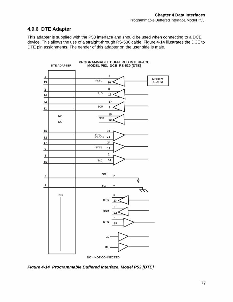
Chapter 4 Data InterfacesProgrammable Buffered Interface/Model P53
77
4.9.6 DTE AdapterThis adapter is supplied with the P53 interface and should be used when connecting to a DCE device. This allows the use of a straight-through RS-530 cable. Figure 4-14 illustrates the DCE to DTE pin assignments. The gender of this adapter on the user side is male.
Figure 4-14 Programmable Buffered Interface, Model P53 [DTE]
PROGRAMMABLE BUFFERED INTERFACEMODEL P53, DCE RS-530 [DTE]
SG
FG
CTS
7
1
84
19
2
14
24
11
15
12
17
9
3
16
7
1
RLSD
RxD
10
3
16
17
9SCR
15
12SCT
FIFOCLOCK
20
23
24
11
2
14
SCTE
TxD
5
13
6
224
19
DSR
RTS
LL
RL
MODEMALARM
DTE ADAPTER
NC
NC
NC
NC = NOT CONNECTED
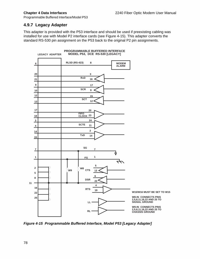
Chapter 4 Data Interfaces 2240 Fiber Optic Modem User ManualProgrammable Buffered Interface/Model P53
78
4.9.7 Legacy AdapterThis adapter is provided with the P53 interface and should be used if preexisting cabling was installed for use with Model P2 interface cards (see Figure 4-15). This adapter converts the standard RS-530 pin assignment on the P53 back to the original P2 pin assignments.
Figure 4-15 Programmable Buffered Interface, Model P53 [Legacy Adapter]
PROGRAMMABLE BUFFERED INTERFACEMODEL P53, DCE RS-530 [LEGACY]
SG
FG
CTS
7
1
8RLSD (RS-423)
RxD3
16
17
9SCR
15
12SCT
FIFOCLOCK
20
23
24
11
2
14
SCTE
TxD
5
13
6
22 4
19
DSR
RTS
LL
RL
MODEMALARM
LEGACY ADAPTER
2
5
8
16
22
25
11
6
20
21
9
10
12
13
17
18
3
4
14
15
7
1
W9W8
W15/W16 MUST BE SET TO W15
W8-IN CONNECTS PINS 2,5,8,11,16,22 AND 25 TO SIGNAL GROUND
W9-IN CONNECTS PINS2,5,8,11,16,22 AND 25 TO CHASSIS GROUND
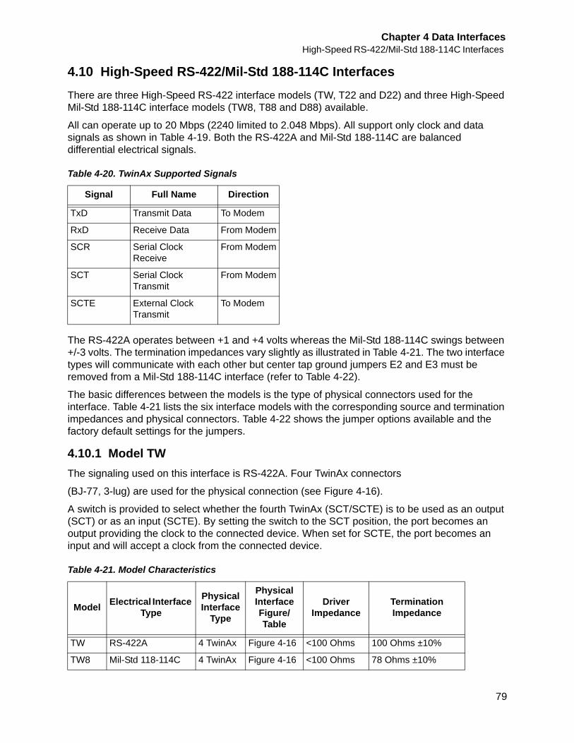
Chapter 4 Data InterfacesHigh-Speed RS-422/Mil-Std 188-114C Interfaces
79
4.10 High-Speed RS-422/Mil-Std 188-114C Interfaces There are three High-Speed RS-422 interface models (TW, T22 and D22) and three High-Speed Mil-Std 188-114C interface models (TW8, T88 and D88) available.
All can operate up to 20 Mbps (2240 limited to 2.048 Mbps). All support only clock and data signals as shown in Table 4-19. Both the RS-422A and Mil-Std 188-114C are balanced differential electrical signals.
The RS-422A operates between +1 and +4 volts whereas the Mil-Std 188-114C swings between +/-3 volts. The termination impedances vary slightly as illustrated in Table 4-21. The two interface types will communicate with each other but center tap ground jumpers E2 and E3 must be removed from a Mil-Std 188-114C interface (refer to Table 4-22).
The basic differences between the models is the type of physical connectors used for the interface. Table 4-21 lists the six interface models with the corresponding source and termination impedances and physical connectors. Table 4-22 shows the jumper options available and the factory default settings for the jumpers.
4.10.1 Model TWThe signaling used on this interface is RS-422A. Four TwinAx connectors
(BJ-77, 3-lug) are used for the physical connection (see Figure 4-16).
A switch is provided to select whether the fourth TwinAx (SCT/SCTE) is to be used as an output (SCT) or as an input (SCTE). By setting the switch to the SCT position, the port becomes an output providing the clock to the connected device. When set for SCTE, the port becomes an input and will accept a clock from the connected device.
Table 4-20. TwinAx Supported Signals
Signal Full Name Direction
TxD Transmit Data To Modem
RxD Receive Data From Modem
SCR Serial Clock Receive
From Modem
SCT Serial Clock Transmit
From Modem
SCTE External Clock Transmit
To Modem
Table 4-21. Model Characteristics
Model Electrical Interface Type
Physical Interface
Type
Physical Interface Figure/Table
Driver Impedance
Termination Impedance
TW RS-422A 4 TwinAx Figure 4-16 <100 Ohms 100 Ohms ±10%
TW8 Mil-Std 118-114C 4 TwinAx Figure 4-16 <100 Ohms 78 Ohms ±10%
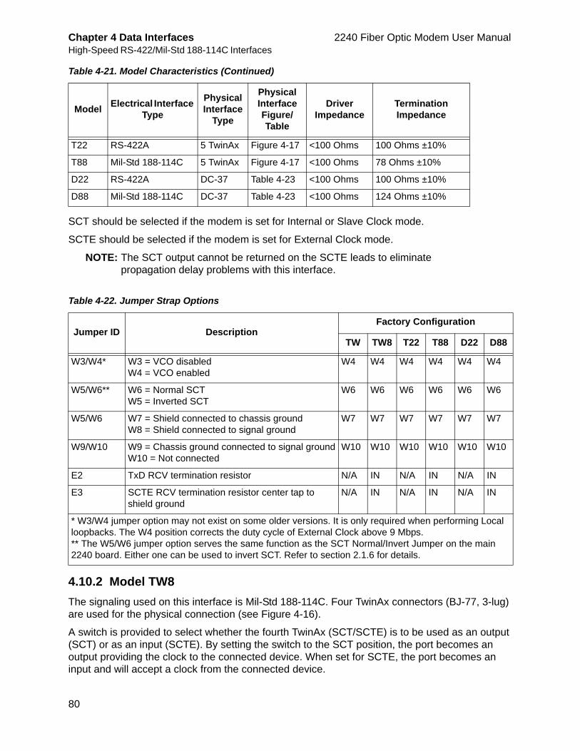
Chapter 4 Data Interfaces 2240 Fiber Optic Modem User ManualHigh-Speed RS-422/Mil-Std 188-114C Interfaces
80
SCT should be selected if the modem is set for Internal or Slave Clock mode.
SCTE should be selected if the modem is set for External Clock mode.
NOTE: The SCT output cannot be returned on the SCTE leads to eliminate propagation delay problems with this interface.
4.10.2 Model TW8The signaling used on this interface is Mil-Std 188-114C. Four TwinAx connectors (BJ-77, 3-lug) are used for the physical connection (see Figure 4-16).
A switch is provided to select whether the fourth TwinAx (SCT/SCTE) is to be used as an output (SCT) or as an input (SCTE). By setting the switch to the SCT position, the port becomes an output providing the clock to the connected device. When set for SCTE, the port becomes an input and will accept a clock from the connected device.
T22 RS-422A 5 TwinAx Figure 4-17 <100 Ohms 100 Ohms ±10%
T88 Mil-Std 188-114C 5 TwinAx Figure 4-17 <100 Ohms 78 Ohms ±10%
D22 RS-422A DC-37 Table 4-23 <100 Ohms 100 Ohms ±10%
D88 Mil-Std 188-114C DC-37 Table 4-23 <100 Ohms 124 Ohms ±10%
Table 4-22. Jumper Strap Options
Jumper ID DescriptionFactory Configuration
TW TW8 T22 T88 D22 D88
W3/W4* W3 = VCO disabled W4 = VCO enabled
W4 W4 W4 W4 W4 W4
W5/W6** W6 = Normal SCTW5 = Inverted SCT
W6 W6 W6 W6 W6 W6
W5/W6 W7 = Shield connected to chassis ground W8 = Shield connected to signal ground
W7 W7 W7 W7 W7 W7
W9/W10 W9 = Chassis ground connected to signal groundW10 = Not connected
W10 W10 W10 W10 W10 W10
E2 TxD RCV termination resistor N/A IN N/A IN N/A IN
E3 SCTE RCV termination resistor center tap to shield ground
N/A IN N/A IN N/A IN
* W3/W4 jumper option may not exist on some older versions. It is only required when performing Local loopbacks. The W4 position corrects the duty cycle of External Clock above 9 Mbps.** The W5/W6 jumper option serves the same function as the SCT Normal/Invert Jumper on the main 2240 board. Either one can be used to invert SCT. Refer to section 2.1.6 for details.
Table 4-21. Model Characteristics (Continued)
Model Electrical Interface Type
Physical Interface
Type
Physical Interface Figure/Table
Driver Impedance
Termination Impedance
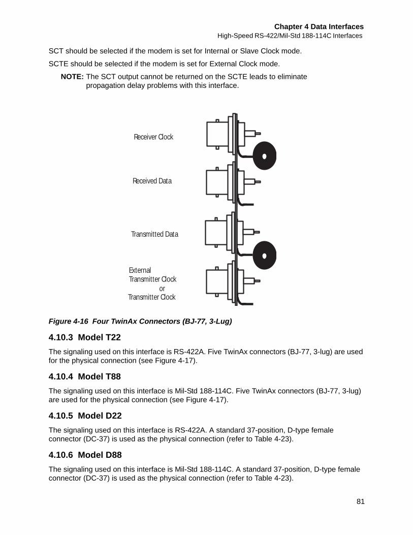
Chapter 4 Data InterfacesHigh-Speed RS-422/Mil-Std 188-114C Interfaces
81
SCT should be selected if the modem is set for Internal or Slave Clock mode.
SCTE should be selected if the modem is set for External Clock mode.
NOTE: The SCT output cannot be returned on the SCTE leads to eliminate propagation delay problems with this interface.
Figure 4-16 Four TwinAx Connectors (BJ-77, 3-Lug)
4.10.3 Model T22The signaling used on this interface is RS-422A. Five TwinAx connectors (BJ-77, 3-lug) are used for the physical connection (see Figure 4-17).
4.10.4 Model T88The signaling used on this interface is Mil-Std 188-114C. Five TwinAx connectors (BJ-77, 3-lug) are used for the physical connection (see Figure 4-17).
4.10.5 Model D22The signaling used on this interface is RS-422A. A standard 37-position, D-type female connector (DC-37) is used as the physical connection (refer to Table 4-23).
4.10.6 Model D88The signaling used on this interface is Mil-Std 188-114C. A standard 37-position, D-type female connector (DC-37) is used as the physical connection (refer to Table 4-23).
Receiver Clock
Received Data
Transmitted Data
Transmitter Clock
ExternalTransmitter Clock
or
Chapter 4 Data Interfaces 2240 Fiber Optic Modem User ManualHigh-Speed RS-422/Mil-Std 188-114C Interfaces
82
Figure 4-17 Five TwinAx Connectors (BJ-77, 3-Lug)
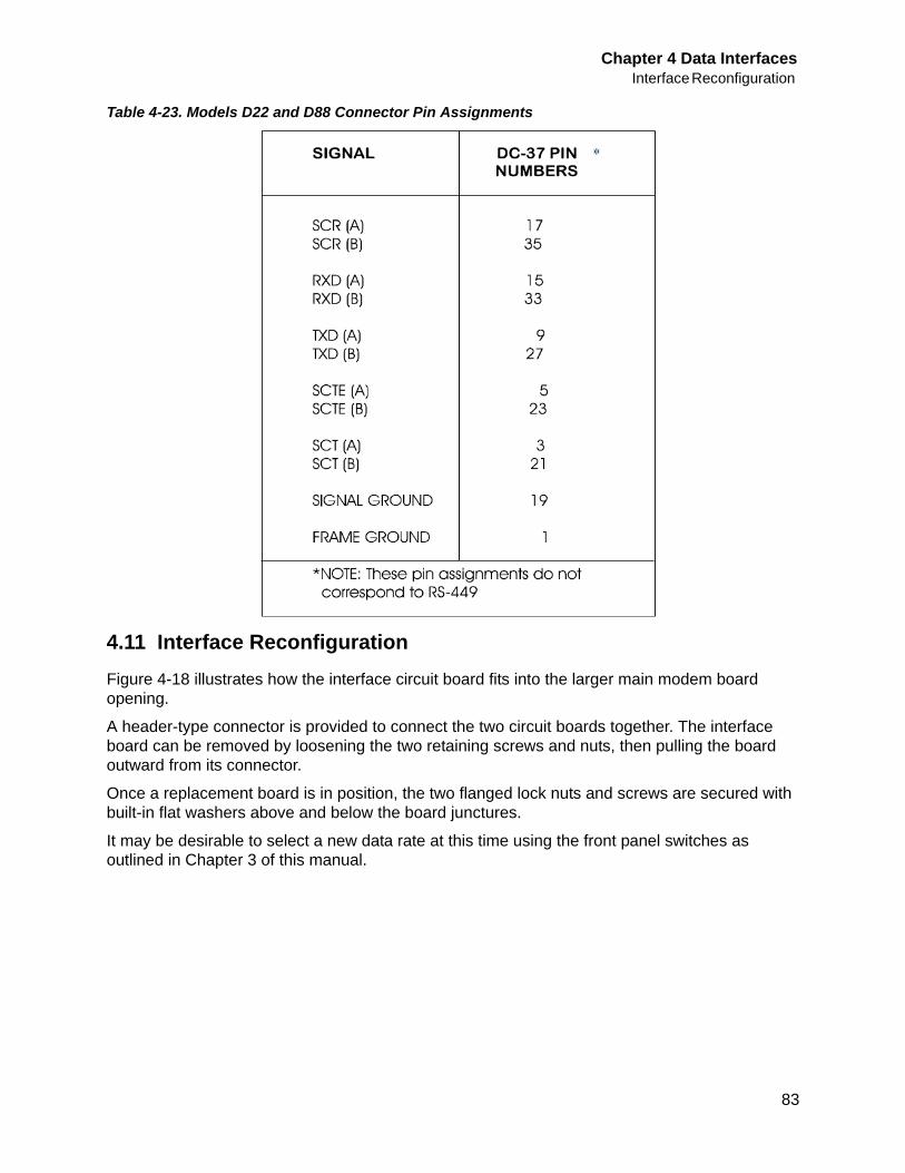
Chapter 4 Data InterfacesInterface Reconfiguration
83
Table 4-23. Models D22 and D88 Connector Pin Assignments
4.11 Interface ReconfigurationFigure 4-18 illustrates how the interface circuit board fits into the larger main modem board opening.
A header-type connector is provided to connect the two circuit boards together. The interface board can be removed by loosening the two retaining screws and nuts, then pulling the board outward from its connector.
Once a replacement board is in position, the two flanged lock nuts and screws are secured with built-in flat washers above and below the board junctures.
It may be desirable to select a new data rate at this time using the front panel switches as outlined in Chapter 3 of this manual.
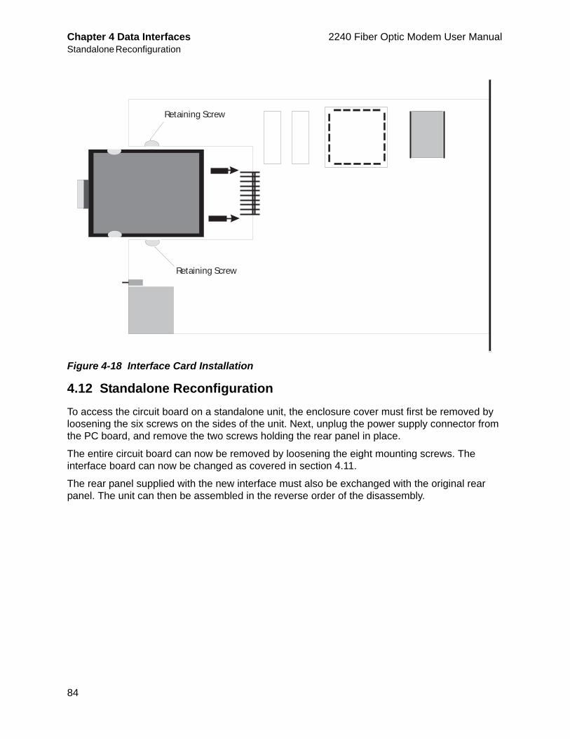
Chapter 4 Data Interfaces 2240 Fiber Optic Modem User ManualStandalone Reconfiguration
84
Figure 4-18 Interface Card Installation
4.12 Standalone ReconfigurationTo access the circuit board on a standalone unit, the enclosure cover must first be removed by loosening the six screws on the sides of the unit. Next, unplug the power supply connector from the PC board, and remove the two screws holding the rear panel in place.
The entire circuit board can now be removed by loosening the eight mounting screws. The interface board can now be changed as covered in section 4.11.
The rear panel supplied with the new interface must also be exchanged with the original rear panel. The unit can then be assembled in the reverse order of the disassembly.
Retaining Screw
Retaining Screw
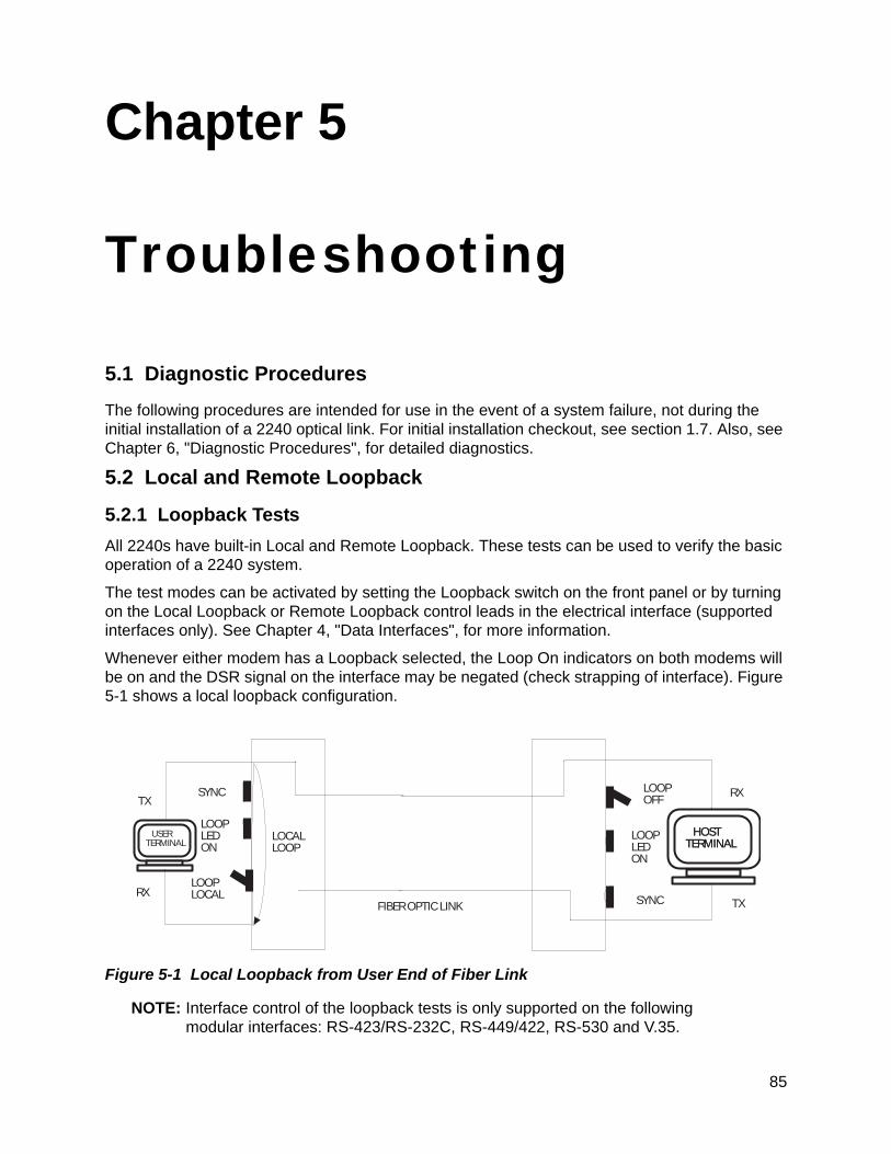
85
Chapter 5
Troubleshooting
5.1 Diagnostic ProceduresThe following procedures are intended for use in the event of a system failure, not during the initial installation of a 2240 optical link. For initial installation checkout, see section 1.7. Also, see Chapter 6, "Diagnostic Procedures", for detailed diagnostics.
5.2 Local and Remote Loopback
5.2.1 Loopback TestsAll 2240s have built-in Local and Remote Loopback. These tests can be used to verify the basic operation of a 2240 system.
The test modes can be activated by setting the Loopback switch on the front panel or by turning on the Local Loopback or Remote Loopback control leads in the electrical interface (supported interfaces only). See Chapter 4, "Data Interfaces", for more information.
Whenever either modem has a Loopback selected, the Loop On indicators on both modems will be on and the DSR signal on the interface may be negated (check strapping of interface). Figure 5-1 shows a local loopback configuration.
Figure 5-1 Local Loopback from User End of Fiber Link
NOTE: Interface control of the loopback tests is only supported on the following modular interfaces: RS-423/RS-232C, RS-449/422, RS-530 and V.35.
HOSTTERMINAL HOSTTERMINAL
USERTERMINAL
TX
RX
RX
TX
LOOPLEDON
LOCALLOOP
LOOPLOCAL
SYNC
SYNC
LOOPOFF
LOOPLEDON
FIBER OPTIC LINK
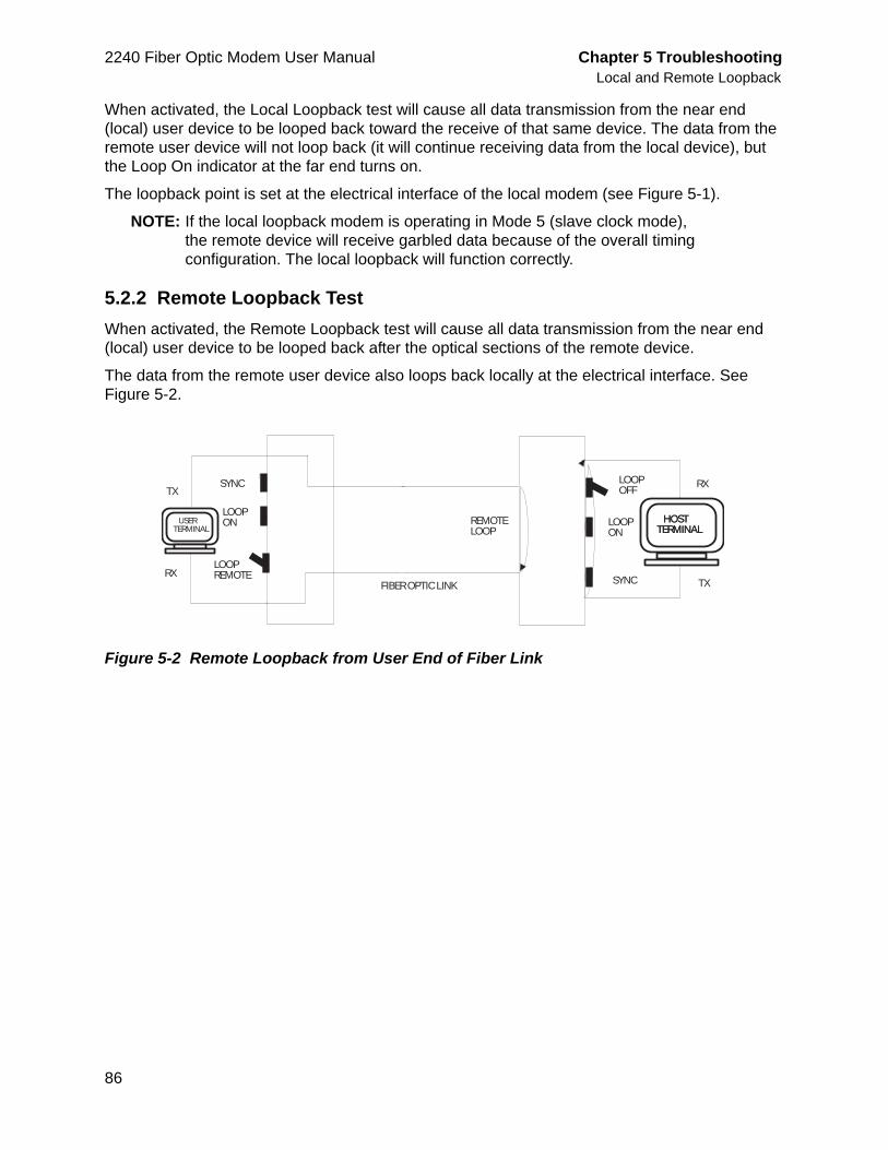
2240 Fiber Optic Modem User Manual Chapter 5 TroubleshootingLocal and Remote Loopback
86
When activated, the Local Loopback test will cause all data transmission from the near end (local) user device to be looped back toward the receive of that same device. The data from the remote user device will not loop back (it will continue receiving data from the local device), but the Loop On indicator at the far end turns on.
The loopback point is set at the electrical interface of the local modem (see Figure 5-1).
NOTE: If the local loopback modem is operating in Mode 5 (slave clock mode), the remote device will receive garbled data because of the overall timing configuration. The local loopback will function correctly.
5.2.2 Remote Loopback TestWhen activated, the Remote Loopback test will cause all data transmission from the near end (local) user device to be looped back after the optical sections of the remote device.
The data from the remote user device also loops back locally at the electrical interface. See Figure 5-2.
Figure 5-2 Remote Loopback from User End of Fiber Link
HOSTTERMINAL HOSTTERMINAL
USERTERMINAL
TX
RX
RX
TX
LOOPON
LOOPREMOTE
SYNC
SYNC
LOOPOFF
LOOPON
FIBER OPTIC LINK
REMOTELOOP

87
Chapter 6
Diagnostic Procedures
6.1 2240/2201 Diagnostic ProceduresThe following diagnostic procedures should be followed to test the 2240 system, troubleshoot a defective link or detect a defective fiber optic cable, connector, modem or power supply.
NOTE: Refer to the 2201 Rack Chassis/2200R Redundant Modem Card User Manual for diagnostic procedures for the 2201 Rack Chassis and power supplies.
6.1.1 Required Equipment• Multimeter - for AC voltage, resistance and continuity tests.
• Fiber Optic Power Meter - should be calibrated at the correct optical wavelength with the appropriate optical connectors.
• A short (one meter or less) fiber optic jumper cable consistent with the modem optics under test, terminated with the appropriate connectors.
• A Bit Error Rate Tester (BERT) with the appropriate electrical interface and cable.
NOTE: Once any power system problems have been corrected, continue the system checkout after the Loopback Diagnostic Procedure.
Step Symptom Possible Causes Action
1 No power indicator on front panel(s)
No AC power Check AC power source
2 No power indicator on front panel(s)
Defective modem Replace Modem
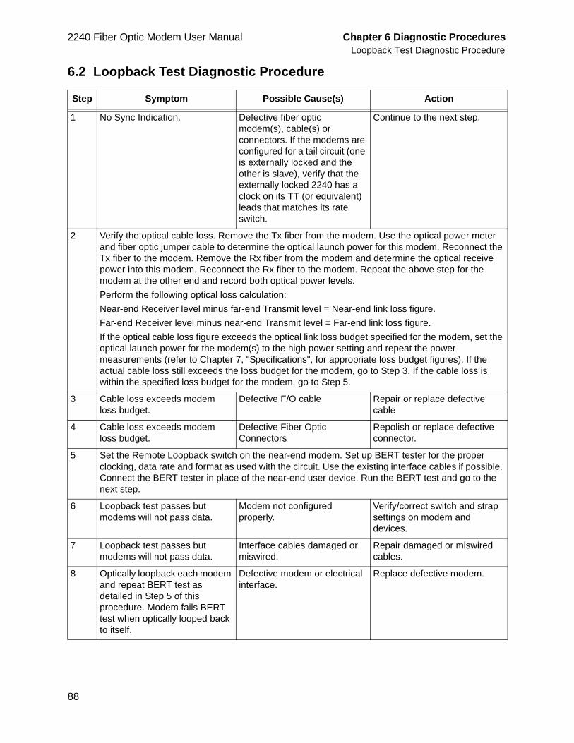
2240 Fiber Optic Modem User Manual Chapter 6 Diagnostic ProceduresLoopback Test Diagnostic Procedure
88
6.2 Loopback Test Diagnostic Procedure
Step Symptom Possible Cause(s) Action
1 No Sync Indication. Defective fiber optic modem(s), cable(s) or connectors. If the modems are configured for a tail circuit (one is externally locked and the other is slave), verify that the externally locked 2240 has a clock on its TT (or equivalent) leads that matches its rate switch.
Continue to the next step.
2 Verify the optical cable loss. Remove the Tx fiber from the modem. Use the optical power meter and fiber optic jumper cable to determine the optical launch power for this modem. Reconnect the Tx fiber to the modem. Remove the Rx fiber from the modem and determine the optical receive power into this modem. Reconnect the Rx fiber to the modem. Repeat the above step for the modem at the other end and record both optical power levels.Perform the following optical loss calculation:Near-end Receiver level minus far-end Transmit level = Near-end link loss figure.Far-end Receiver level minus near-end Transmit level = Far-end link loss figure.If the optical cable loss figure exceeds the optical link loss budget specified for the modem, set the optical launch power for the modem(s) to the high power setting and repeat the power measurements (refer to Chapter 7, "Specifications", for appropriate loss budget figures). If the actual cable loss still exceeds the loss budget for the modem, go to Step 3. If the cable loss is within the specified loss budget for the modem, go to Step 5.
3 Cable loss exceeds modem loss budget.
Defective F/O cable Repair or replace defective cable
4 Cable loss exceeds modem loss budget.
Defective Fiber Optic Connectors
Repolish or replace defective connector.
5 Set the Remote Loopback switch on the near-end modem. Set up BERT tester for the proper clocking, data rate and format as used with the circuit. Use the existing interface cables if possible. Connect the BERT tester in place of the near-end user device. Run the BERT test and go to the next step.
6 Loopback test passes but modems will not pass data.
Modem not configured properly.
Verify/correct switch and strap settings on modem and devices.
7 Loopback test passes but modems will not pass data.
Interface cables damaged or miswired.
Repair damaged or miswired cables.
8 Optically loopback each modem and repeat BERT test as detailed in Step 5 of this procedure. Modem fails BERT test when optically looped back to itself.
Defective modem or electrical interface.
Replace defective modem.

Chapter 6 Diagnostic ProceduresFiber Optic Diagnostic Procedure
89
6.3 Fiber Optic Diagnostic ProcedureIf the Loopback Test is successful, and the modems still do not function, check the fiber optic parameters as outlined below. There also may be a data rate incompatibility. If this check out of the electrical and optical links provides no indication as to the problem, contact Canoga Perkins Installation and Repair Department for assistance.
NOTE: Each range limit has a +1dB margin at the transition point.
The following are some additional checkpoints to consider about fiber optics:
• Are you using a fiber optic link of less than the High Power Loss Budget? (Refer to Table 6-1.) Set the optical power switch to LO.
• Are you using a fiber optic link of more than the Low Power Loss Budget? (Refer to Table 6-1.) Set the optical power switch to HI.
• Are the fiber optic cables marked correctly? Connect Tx cable to Tx connector, Rx to the Rx connector. If Local and Remote Sync indicators do not come on, try swapping cables at one end of link.
• Is the data rate set correctly?
• Are you using the correct clock mode (internal/external) for synchronous transmission or are you using asynchronous transmission?
NOTE: The 1310 nm LP laser does not have a HI/LO power switch.
9 Set the Local Loopback switch on the near-end modem. Modem fails BERT when looped locally.
Defective modem or electrical interface.
Replace defective modem.
Table 6-1. Link Loss Range
ModelLink Loss Range
HI Power LO Power
850 nm Standard >6 dB to Max <6 dB
1310 nm HP laser >6 dB to Max <6 dB
Step Symptom Possible Cause(s) Action

2240 Fiber Optic Modem User Manual Chapter 6 Diagnostic ProceduresFiber Optic Diagnostic Procedure
90
91
Chapter 7
Specifications
7.1 Optical Interface
Composite Error Rate 1 in 1010 or better
Fiber optic cable compatibility 50 and 62.5 micron multimode or 8 to 10 micron single mode fiber
Transmitter LED (850nm)Laser diode (1310nm)
HI/LO optical power switch Reduces transmit power to accommodate a zero loss link
Wavelength 850 or 1310 nanometers
Fiber optic connector ST or FC type
Fiber optic receiver:850nm standard1310nm laserTransmission code
PIN diodePIN (InGaAs)Biphase multiplexed
Typical fiber optic link loss budget:850nm LED1310nm LP laser1310nm HP laser
15 dB with 62.5/125 mm fiber13 dB with 8 or 10/125 sm fiber or 62.5/125 mm fiber25 dB with 8 or 10/125 sm fiber or 62.5/125 mm fiber
2240 Fiber Optic Modem User Manual Chapter 7 SpecificationsOptical Interface
92
Tabl
e 7-
1. O
ptic
al In
terf
ace
Des
crip
tion
Mod
elD
escr
iptio
nC
onne
ctor
Ty
peW
avel
engt
h
Laun
ch
Pow
er
(dB
m)
Rec
eive
r Se
ns.
(dB
m)
Rec
eive
r O
verd
rive
(dB
m)
Min
. Los
s B
udge
tM
inM
ax
2240
-x-x
xx-0
1-xx
-115
dB
MM
,LE
DS
T85
0 nm
-17.
0-1
3.0
-32.
0-1
5.0
15 d
B
2240
-x-x
xx-1
6-xx
-113
dB
SM
/MM
, LP
lase
rS
T, F
C-P
C13
10 n
m-1
9.0
-14.
0-3
2.0
-12.
013
dB
2240
-x-x
xx-1
1-xx
-125
dB
SM
/MM
, H
P la
ser
ST,
FC
-PC
1310
nm
-5.0
-4.7
-32.
0-1
2.0
27 d
B
Chapter 7 SpecificationsSystem Electrical
93
7.1.1 Distance Guide
NOTE: These typical distances depend on the quality of the fiber cable plant.
7.2 System ElectricalInterface Connector
Interface Connector Type
RS-232C/423/530 female DB-25
Programmable RS-530 (P53) female DB-25
RS-422 (422) female DC-37
CCITT V.35 (V.36) female 34-pin Winchester
TTL/BNC four female BNC coaxial
RS-422 Mil-Std 188-114C four or five female Twinaxial connectors BJ-77 (3-lug)
Transparent T1/E1 Female DA-15, two female BNC connectors or terminal strip
Interfaces supported RS-232D/RS-423RS-449CCITT V.35TTL/BNCProgrammable RS-422 (P)TwinAx 422TwinAx MIL-STD-188-114CDC-37 MIL-STD-188-114Transparent T1/E1CCITT V.35/RS-423 (MC2), RS-449/423 (MC1)RS-530
1310 nm HP SMF
0
1310 nm HP laser SMF
1310 nm LP laser SMF
1310 nm LP laser MMF
850 nm LED MMF
10 20 30Kilometers
40 50 60 70 80 90 100
2240 Fiber Optic Modem User Manual Chapter 7 SpecificationsIndicators and Controls
94
Power Requirement
7.3 Indicators and Controls
7.4 Physical and Environmental
Standalone 115 VAC +10% @ 0.22 amps115/230 VAC + 10% [email protected] amps 47 to 63 Hz
Rack mount PC card 18 VAC +10% @ 1.1 amps per board50 to 64 Hz
Indicators (6) Tx/Rx data activityLocal/remote syncLoopback activePower onPower alarms (2201 Rack only)
Controls (10) Local/remote loopback slide switchOperating mode DIP switchData rate DIP switchHi/Low optic power DIP switch
Dimensions:2240-S StandalonePC Card
12.8" L x 8.5" W x 2.5" H12.5" L x 7.8" W x 1.06" H
Unit Weights (shipping):2240-S Standalone PC Card
3.63 lbs0.9 lbs
Operating Environment: TemperatureHumidity
0 to 50° C0 to 95% non-condensing
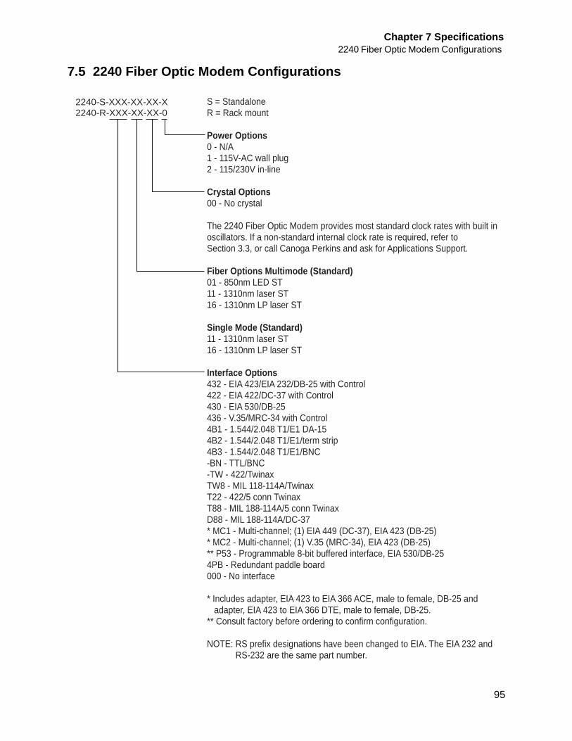
Chapter 7 Specifications2240 Fiber Optic Modem Configurations
95
7.5 2240 Fiber Optic Modem Configurations
S = StandaloneR = Rack mount Power Options0 - N/A1 - 115V-AC wall plug2 - 115/230V in-line
Crystal Options00 - No crystal
The 2240 Fiber Optic Modem provides most standard clock rates with built inoscillators. If a non-standard internal clock rate is required, refer to Section 3.3, or call Canoga Perkins and ask for Applications Support.
Fiber Options Multimode (Standard) 01 - 850nm LED ST 11 - 1310nm laser ST16 - 1310nm LP laser ST
Single Mode (Standard)11 - 1310nm laser ST16 - 1310nm LP laser ST
Interface Options432 - EIA 423/EIA 232/DB-25 with Control422 - EIA 422/DC-37 with Control430 - EIA 530/DB-25436 - V.35/MRC-34 with Control4B1 - 1.544/2.048 T1/E1 DA-15 4B2 - 1.544/2.048 T1/E1/term strip 4B3 - 1.544/2.048 T1/E1/BNC-BN - TTL/BNC-TW - 422/TwinaxTW8 - MIL 118-114A/TwinaxT22 - 422/5 conn TwinaxT88 - MIL 188-114A/5 conn TwinaxD88 - MIL 188-114A/DC-37* MC1 - Multi-channel; (1) EIA 449 (DC-37), EIA 423 (DB-25)* MC2 - Multi-channel; (1) V.35 (MRC-34), EIA 423 (DB-25)** P53 - Programmable 8-bit buffered interface, EIA 530/DB-254PB - Redundant paddle board000 - No interface
* Includes adapter, EIA 423 to EIA 366 ACE, male to female, DB-25 and adapter, EIA 423 to EIA 366 DTE, male to female, DB-25.** Consult factory before ordering to confirm configuration.
NOTE: RS prefix designations have been changed to EIA. The EIA 232 and RS-232 are the same part number.
2240-S-XXX-XX-XX-X 2240-R-XXX-XX-XX-0

Chapter 7 Specifications 2240 Fiber Optic Modem User Manual2240 Fiber Optic Modem Configurations
96


CANOGA PERKINS CORPORATION
20600 Prairie StreetChatsworth, California 91311-6008 USA
Phone: (818) 718-6300 FAX: (818) 718-6312Website: www.canoga.comEmail: [email protected]