24 ghz, ism band, multichannel fmcw radar transmitter data
TRANSCRIPT

24 GHz, ISM Band, MultichannelFMCW Radar Transmitter
Data Sheet ADF5902
Rev. A Document Feedback Information furnished by Analog Devices is believed to be accurate and reliable. However, no responsibility is assumed by Analog Devices for its use, nor for any infringements of patents or other rights of third parties that may result from its use. Specifications subject to change without notice. No license is granted by implication or otherwise under any patent or patent rights of Analog Devices. Trademarks and registered trademarks are the property of their respective owners.
One Technology Way, P.O. Box 9106, Norwood, MA 02062-9106, U.S.A.Tel: 781.329.4700 ©2018–2020 Analog Devices, Inc. All rights reserved. Technical Support www.analog.com
FEATURES 24 GHz to 24.25 GHz VCO (industrial, scientific, and medical
(ISM) radio band) 2-channel 24 GHz power amplifier with 8 dBm output Single-ended outputs 2-channel muxed outputs with mute function Programmable output power LO output buffer RF frequency range: 24 GHz to 24.25 GHz Power control detector Auxiliary 8-bit ADC High and low speed FMCW ramp generation 25-bit fixed modulus allows subhertz frequency resolution PFD frequencies up to 110 MHz Normalized phase noise floor of −222 dBc/Hz Programmable charge pump currents ±5°C temperature sensor 4-wire SPI ESD performance
HBM: 2000 V CDM: 250 V
Qualified for automotive applications
APPLICATIONS Automotive radars Industrial radars Microwave radar sensors
GENERAL DESCRIPTION The ADF5902 is a 24 GHz transmitter (Tx) monolithic microwave integrated circuit (MMIC) with an on-chip, 24 GHz voltage controlled oscillator (VCO). The VCO features a fractional-N frequency synthesizer with waveform generation capability with programmable grid array (PGA) and dual transmitter channels for radar systems. The on-chip, 24 GHz VCO generates the 24 GHz signal for the two transmitter channels and the local oscillator (LO) output. Each transmitter channel contains a power control circuit. There is also an on-chip temperature sensor.
Control of all the on-chip registers is through a simple, 4-wire serial peripheral interface (SPI).
The ADF5902 comes in a compact, 32-lead, 5 mm × 5 mm LFCSP package.
FUNCTIONAL BLOCK DIAGRAM
16
746
-00
1
TXOUT1
TXOUT2
LOOUTVTUNE
RSET
GND
TX_AHI
ATEST
RF_AHI AHI DVDD VREGC1 C2
MUXOUT
VCO_AHI
REFIN
N DIVIDER
VCOCAL
R DIVIDER
TEMPERATURESENSOR
ADC
÷2
BIASREGULATOR
ADC
ADC
ADF5902
+ PHASEFREQUENCYDETECTOR
READBACKCONTROL
ADC OUTPUT
FREQUENCY COUNTER
CHARGEPUMP
–
CPOUT
32-BITDATA
REGISTERDOUT
LE
DATA
CLK
CE
THIRD-ORDERFRACTIONAL
INTERPOLATOR
RAMPGENERATION
TX_DATA
CP_AHI
RDIVNDIV
RAMPSTATUS
DVDDGND
FMCW RAMP GENERATION PLL
Figure 1.

ADF5902 Data Sheet
Rev. A | Page 2 of 39
TABLE OF CONTENTS Features .............................................................................................. 1
Applications ....................................................................................... 1
General Description ......................................................................... 1
Functional Block Diagram .............................................................. 1
Revision History ............................................................................... 2
Specifications ..................................................................................... 3
Timing Specifications .................................................................. 5
Absolute Maximum Ratings ............................................................ 6
Thermal Resistance ...................................................................... 6
ESD Caution .................................................................................. 6
Pin Configuration and Function Descriptions ............................. 7
Typical Performance Characteristics ............................................. 9
Theory of Operation ...................................................................... 11
Reference Input Section ............................................................. 11
RF INT Divider ........................................................................... 11
INT, FRAC, and R Relationship ............................................... 11
R Counter .................................................................................... 11
PFD and Charge Pump .............................................................. 11
Input Shift Register..................................................................... 11
Program Modes .......................................................................... 12
Register Maps .................................................................................. 13
Register 0 ..................................................................................... 16
Register 1 ..................................................................................... 17
Register 2 ..................................................................................... 18
Register 3 ..................................................................................... 19
Register 4 ..................................................................................... 20
Register 5 ..................................................................................... 21
Register 6 ..................................................................................... 22
Register 7 ..................................................................................... 23
Register 8 ..................................................................................... 24
Register 9 ..................................................................................... 24
Register 10 ................................................................................... 25
Register 11 ................................................................................... 25
Register 12 ................................................................................... 26
Register 13 ................................................................................... 27
Register 14 ................................................................................... 28
Register 15 ................................................................................... 29
Register 16 ................................................................................... 30
Register 17 ................................................................................... 30
Applications Information .............................................................. 31
Initialization Sequence .............................................................. 31
Recalibration Sequence ............................................................. 32
Temperature Sensor ................................................................... 33
RF Synthesis: A Worked Example ............................................ 33
Reference Doubler ...................................................................... 33
Frequency Measurement Procedure ........................................ 34
Waveform Generation ............................................................... 34
Waveform Deviations and Timing ........................................... 34
Ramp and Modulation ............................................................... 35
Application of the ADF5902 in FMCW Radar ...................... 37
Outline Dimensions ....................................................................... 39
Ordering Guide .......................................................................... 39
Automotive Products ................................................................. 39
REVISION HISTORY 1/2020—Rev. 0 to Rev. A Changes to Figure 23 ...................................................................... 15 Changes to Figure 41 ...................................................................... 30 11/2018—Revision 0: Initial Version
Data Sheet ADF5902
Rev. A | Page 3 of 39
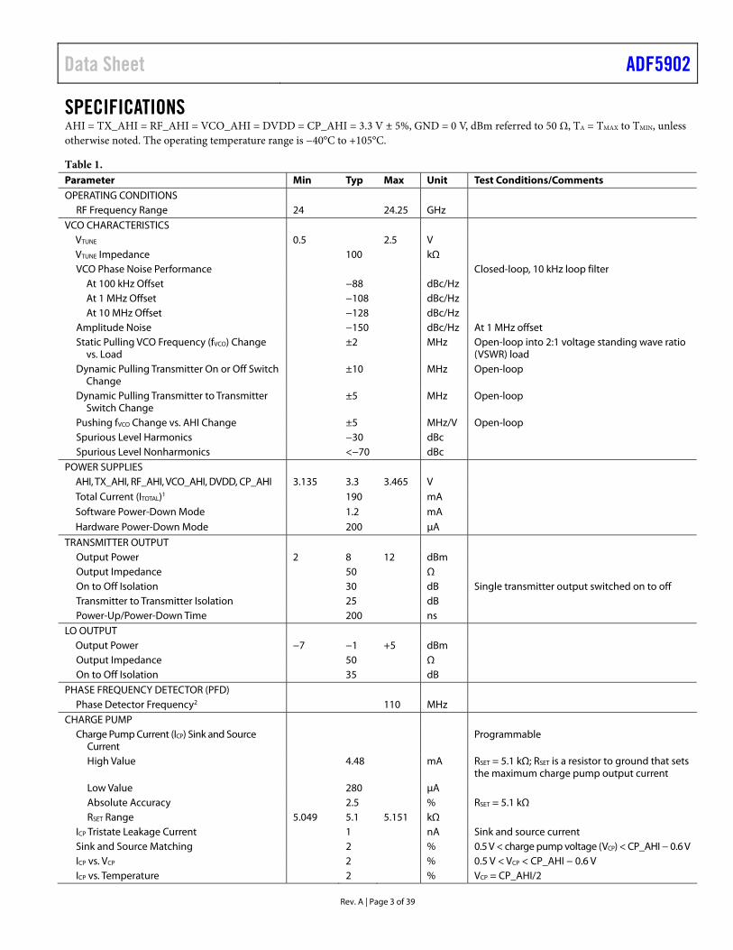
SPECIFICATIONS AHI = TX_AHI = RF_AHI = VCO_AHI = DVDD = CP_AHI = 3.3 V ± 5%, GND = 0 V, dBm referred to 50 Ω, TA = TMAX to TMIN, unless otherwise noted. The operating temperature range is −40°C to +105°C.
Table 1. Parameter Min Typ Max Unit Test Conditions/Comments OPERATING CONDITIONS
RF Frequency Range 24 24.25 GHz VCO CHARACTERISTICS
VTUNE 0.5 2.5 V VTUNE Impedance 100 kΩ VCO Phase Noise Performance Closed-loop, 10 kHz loop filter
At 100 kHz Offset −88 dBc/Hz At 1 MHz Offset −108 dBc/Hz At 10 MHz Offset −128 dBc/Hz
Amplitude Noise −150 dBc/Hz At 1 MHz offset Static Pulling VCO Frequency (fVCO) Change
vs. Load ±2 MHz Open-loop into 2:1 voltage standing wave ratio
(VSWR) load Dynamic Pulling Transmitter On or Off Switch
Change ±10 MHz Open-loop
Dynamic Pulling Transmitter to Transmitter Switch Change
±5 MHz Open-loop
Pushing fVCO Change vs. AHI Change ±5 MHz/V Open-loop Spurious Level Harmonics −30 dBc Spurious Level Nonharmonics <−70 dBc
POWER SUPPLIES AHI, TX_AHI, RF_AHI, VCO_AHI, DVDD, CP_AHI 3.135 3.3 3.465 V Total Current (ITOTAL)1 190 mA Software Power-Down Mode 1.2 mA Hardware Power-Down Mode 200 μA
TRANSMITTER OUTPUT Output Power 2 8 12 dBm Output Impedance 50 Ω On to Off Isolation 30 dB Single transmitter output switched on to off Transmitter to Transmitter Isolation 25 dB Power-Up/Power-Down Time 200 ns
LO OUTPUT Output Power −7 −1 +5 dBm Output Impedance 50 Ω On to Off Isolation 35 dB
PHASE FREQUENCY DETECTOR (PFD) Phase Detector Frequency2 110 MHz
CHARGE PUMP Charge Pump Current (ICP) Sink and Source
Current Programmable
High Value 4.48 mA RSET = 5.1 kΩ; RSET is a resistor to ground that sets the maximum charge pump output current
Low Value 280 μA Absolute Accuracy 2.5 % RSET = 5.1 kΩ RSET Range 5.049 5.1 5.151 kΩ
ICP Tristate Leakage Current 1 nA Sink and source current Sink and Source Matching 2 % 0.5 V < charge pump voltage (VCP) < CP_AHI − 0.6 V ICP vs. VCP 2 % 0.5 V < VCP < CP_AHI − 0.6 V ICP vs. Temperature 2 % VCP = CP_AHI/2

ADF5902 Data Sheet
Rev. A | Page 4 of 39
Parameter Min Typ Max Unit Test Conditions/Comments NOISE CHARACTERISTICS
Normalized Phase Noise Floor, Fractional-N Mode3
−222 dBc/Hz PLL loop bandwidth (BW) = 1 MHz
Normalized 1/f Noise (PN1_f)4 −120 dBc/Hz Measured at 10 kHz offset, normalized to 1 GHz TEMPERATURE SENSOR
Analog Accuracy ±5 °C Following one point calibration Digital Accuracy ±5 °C Following one point calibration Sensitivity 6.4 mV/°C
ANALOG-TO-DIGITAL CONVERTER (ADC) Resolution 8 Bits Integral Nonlinearity (INL) ±1 LSB Differential Nonlinearity (DNL) ±1 LSB Least Significant Bit (LSB) 7.4 mV
REFIN CHARACTERISITICS REFIN Input Frequency 10 260 MHz −5 dBm minimum to +9 dBm maximum biased
at AHI/2 (ac coupling ensures 1.8 ÷ 2 bias); for frequencies < 10 MHz, use a dc-coupled, CMOS-compatible square wave with a slew rate > 25 V/μs
REFIN Input Capacitance2 1.2 pF REFIN Input Current ±100 μA
LOGIC INPUTS Input Voltage
High (VIH) 1.4 V Low (VIL) 0.6 V
Input Current (IINH, IINL) ±1 μA Input Capacitance (CIN)2 10 pF
LOGIC OUTPUTS Output Voltage
High (VOH)5 DVDD − 0.4
V
Low (VOL) 0.4 V Output Current
High (IOH) 500 μA Low (IOL) 500 μA
1 Following the initialization sequence described in the Initialization Sequence section, TA = 25°C, AHI = 3.3 V, fREFIN = 100 MHz, and RF = 24.025 GHz. 2 Guaranteed by design. Sample tested to ensure compliance. 3 This specification can be used to calculate phase noise for any application. Use the formula ((Normalized Phase Noise Floor) + 10 log(fPFD) + 20 logN) to calculate
in-band phase noise performance as seen at the VCO output. 4 The PLL phase noise is composed of flicker (1/f) noise plus the normalized PLL noise floor. The formula for calculating the 1/f noise contribution at an RF frequency (fRF)
and at an offset frequency (f) is given by PN = PN1_f + 10 log(10 kHz/f) + 20 log(fRF/1 GHz). Both the normalized phase noise floor and flicker noise are modeled in ADIsimPLL. 5 DVDD selected from the IO level bit (Bit DB11 in Register 3).

Data Sheet ADF5902
Rev. A | Page 5 of 39
TIMING SPECIFICATIONS Write Timing Specifications
AHI = TX_AHI = RF_AHI = VCO_AHI = DVDD = CP_AHI = 3.3 V ± 5%, GND = 0 V, dBm referred to 50 Ω, TA = TMIN to TMAX, unless otherwise noted. The operating temperature range is −40°C to +105°C.
Table 2. Parameter Limit at TMIN to TMAX Unit Description t1 20 ns min LE setup time t2 10 ns min DATA to CLK setup time t3 10 ns min DATA to CLK hold time t4 25 ns min CLK high duration t5 25 ns min CLK low duration t6 10 ns min CLK to LE setup time t7 20 ns min LE pulse width t8 10 ns max LE setup time to DOUT t9 15 ns max CLK setup time to DOUT
CLK
DATA
LE
DB30DB1
(CONTROL BIT C2)DB2
(CONTROL BIT C3)DB0 (LSB)
(CONTRO BIT C1)
1
t2 t3
t4 t5
7
6
DB31 (MSB)
DB0DB1
8
9
DB31(MSB)
DB30DOUT
1674
6-0
02
Figure 2. Write Timing Diagram
500µA IOL
500µA IOH
DVDD/2TO DOUT ANDMUXOUT PINS
CL10pF
16
746
-00
3
Figure 3. Load Circuit for DOUT/MUXOUT Timing, CL = 10 pF

ADF5902 Data Sheet
Rev. A | Page 6 of 39
ABSOLUTE MAXIMUM RATINGS Table 3. Parameter Rating AHI to GND −0.3 V to +3.9 V AHI to TX_AHI −0.3 V to +0.3 V AHI to RF_AHI −0.3 V to +0.3 V AHI to VCO_AHI −0.3 V to +0.3 V AHI to DVDD −0.3 V to +0.3 V AHI to CP_AHI −0.3 V to +0.3 V VTUNE to GND −0.3 V to +3.6 V Digital Input/Output Voltage to GND −0.3 V to DVDD + 0.3 V Operating Temperature Range −40°C to +105°C Storage Temperature Range −65°C to +150°C Maximum Junction Temperature 150°C Reflow Soldering
Peak Temperature 260°C Time at Peak Temperature 40 sec
Electrostatic Discharge (ESD) Charged Device Model (CDM) 250 V Human Body Model (HBM) 2000 V
Stresses at or above those listed under Absolute Maximum Ratings may cause permanent damage to the product. This is a stress rating only; functional operation of the product at these or any other conditions above those indicated in the operational section of this specification is not implied. Operation beyond the maximum operating conditions for extended periods may affect product reliability.
The ADF5902 is a high performance RF integrated circuit with an ESD rating of 2 kV and is ESD sensitive. Take proper precautions for handling and assembly.
THERMAL RESISTANCE Thermal performance is directly linked to printed circuit board (PCB) design and operating environment. Careful attention to PCB thermal design is required.
Table 4. Thermal Resistance Package Type θJA
1 θJC2 Unit
CP-32-123 48.18 26.86 °C/W
1 θJA is the natural convection junction-to-ambient thermal resistance measured in a one cubic foot sealed enclosure.
2 θJC is the junction-to-case thermal resistance. 3 Test Condition 1: thermal impedance simulated values are based on use of a
PCB with the thermal impedance pad soldered to GND.
ESD CAUTION

Data Sheet ADF5902
Rev. A | Page 7 of 39
PIN CONFIGURATION AND FUNCTION DESCRIPTIONS
GND
NOTES1. THE EXPOSED PAD MUST BE CONNECTED TO GND.
TXOUT1
GNDTX_AHITX_AHI
GNDTXOUT2
GND
DOUTLEDATACLKCETX_DATAVREGDVDD
AT
ES
TG
ND
LO
OU
TG
ND
GN
DR
F_A
HI
RE
FIN
AH
I
C2
C1
VC
O_A
HI
VT
UN
EC
PO
UT
CP
_AH
IR
SE
TM
UX
OU
T
2423222120191817
12345678
9 10 11 12 13 14 15 16
32 31 30 29 28 27 26 25
ADF5902TOP VIEW
(Not to Scale)
167
46-0
04
Figure 4. Pin Configuration
Table 5. Pin Function Descriptions Pin No. Mnemonic Description 1, 3, 6, 8, 10,
12, 13 GND RF Ground. Tie all GND pins together.
2 TXOUT1 24 GHz Transmitter Output 1. 4, 5 TX_AHI Voltage Supply for the Transmitter Section. Connect decoupling capacitors (0.1 μF, 1 nF, and 10 pF) to the
ground plane as close as possible to this pin. TX_AHI must be the same value as AHI. 7 TXOUT2 24 GHz Transmitter Output 2. 9 ATEST Analog Test Output Pin. 11 LOOUT LO Output. 14 RF_AHI Voltage Supply for the RF Section. Connect decoupling capacitors (0.1 μF, 1 nF, and 10 pF) to the ground
plane as close as possible to this pin. RF_AHI must be the same value as AHI. 15 REFIN Reference Input. This pin is a CMOS input with a nominal threshold of DVDD/2 and a dc equivalent input
resistance of 100 kΩ. See Figure 17. This input can be driven from a TTL or CMOS crystal oscillator, or it can be ac-coupled.
16 AHI Voltage Supply for the Analog Section. Connect decoupling capacitors (0.1 μF, 1 nF, and 10 pF) to the ground plane as close as possible to this pin.
17 DVDD Digital Power Supply. This supply may range from 3.135 V to 3.465 V. Place decoupling capacitors (0.1 μF, 1 nF, and 10 pF) to the ground plane as close as possible to this pin. DVDD must be the same value as AHI.
18 VREG Internal 1.8 V Regulator Output. Connect a 220 nF capacitor to ground as close as possible to this pin. 19 TX_DATA Transmit Data Pin. This pin controls some of the ramping functionality. Synchronize the rising edge of the
TX_DATA signal to the rising edge of REFIN. 20 CE Chip Enable. A logic low on this pin powers down the device. Taking the pin high powers up the device. 21 CLK Serial Clock Input. This serial clock input clocks in the serial data to the registers. The data is latched into the
32-bit shift register on the CLK rising edge. This input is a high impedance CMOS input. 22 DATA Serial Data Input. The serial data is loaded MSB first with the four LSBs as the control bits. This input is a
high impedance CMOS input. 23 LE Load Enable, CMOS Input. When LE goes high, the data stored in the shift registers is loaded to one of the
18 latches with the latch selected via the control bits. 24 DOUT Serial Data Output. 25 MUXOUT Multiplexer Output. This multiplexer output allows various internal signals to be accessed externally. 26 RSET Resistor Setting Pin. Connecting a 5.1 kΩ resistor between this pin and GND sets an internal current. The
nominal voltage potential at the RSET pin is 0.62 V. 27 CP_AHI Charge Pump Power Supply. This supply may range from 3.135 V to 3.465 V. Place decoupling capacitors
(0.1 μF, 1 nF, and 10 pF) to the ground plane as close as possible to this pin. CP_AHI must be the same value as AHI.
28 CPOUT Charge Pump Output. When the charge pump is enabled, this output provides ±ICP to the external loop filter, which, in turn, drives the VCO.

ADF5902 Data Sheet
Rev. A | Page 8 of 39
Pin No. Mnemonic Description 29 VTUNE Control Input to the VCO. This voltage determines the output. 30 VCO_AHI Voltage Supply for the VCO Section. Connect decoupling capacitors (0.1 μF, 1 nF, and 10 pF) to the ground
plane as close as possible to this pin. VCO_AHI must be the same value as AHI. 31 C1 Decoupling Capacitor 1. Place a 47 nF capacitor to ground as close as possible to this pin. 32 C2 Decoupling Capacitor 2. Place a 220 nF capacitor to ground as close as possible to this pin. EP Exposed Pad. The exposed pad must be connected to GND.

Data Sheet ADF5902
Rev. A | Page 9 of 39
TYPICAL PERFORMANCE CHARACTERISTICS
0
2
4
6
8
10
12
23.95 24.00 24.05 24.10 24.15 24.20 24.25 24.30
Tx
OU
TP
UT
PO
WE
R (
dB
m)
OUTPUT FREQUENCY (GHz)
–40°C+25°C+105°C
Tx1
Tx2
OUTSIDE OF SPECIFIED RANGE
167
46-0
05
Figure 5. Transmitter (Tx) Output Power vs. Output Frequency
0
2
4
6
8
10
12
23.95 24.00 24.05 24.10 24.15 24.20 24.25 24.30
Tx1
OU
TP
UT
PO
WE
R (
dB
m)
OUTPUT FREQUENCY (GHz)
–40°C+25°C+105°C
3.300V3.465V
3.135V
OUTSIDE OF SPECIFIED RANGE
167
46-0
06
Figure 6. Transmitter 1 (Tx1) Output Power Variation vs. Output Frequency with Temperature and Supply
–20
–15
–10
–5
0
5
10
15
0 10 20 30 40 50 60 70 80 90 100
Tx
OU
TP
UT
PO
WE
R (
dB
m)
Tx AMPLITUDE CALIBRATION REFERENCE CODE
–40°C+25°C+105°C
167
46-0
07
Figure 7. Transmitter (Tx) Output Power vs. Transmitter (Tx) Amplitude Calibration Reference Code
–8
–6
–4
–2
0
4
2
6
23.95 24.00 24.05 24.10 24.15 24.20 24.25 24.30
LO
OU
TP
UT
PO
WE
R (
dB
m)
OUTPUT FREQUENCY (GHz)
–40°C+25°C+105°COUTSIDE OF SPECIFIED RANGE
167
46-0
08
Figure 8. LO Output Power vs. Output Frequency
24.000
24.050
24.100
24.150
24.200
24.250
0 100 200 300 400 500 600
FR
EQ
UE
NC
Y(G
Hz)
TIME (µs) 167
46-
00
9
Figure 9. Triangular Ramp with Delay
0 100 200 300 400 500 600
TIME (µs) 167
46-
01
024.000
24.050
24.100
24.150
24.200
24.250
FR
EQ
UE
NC
Y(G
Hz)
Figure 10. Dual Triangular Ramp

ADF5902 Data Sheet
Rev. A | Page 10 of 39
0 100 200 300 400 500 600
TIME (µs) 167
46-1
0924.000
24.050
24.100
24.150
24.200
24.300
24.250
FR
EQ
UE
NC
Y(G
Hz)
Figure 11. Sawtooth Ramp
0
0.5
1.0
1.5
2.0
2.5
3.0
3.5
24.00 24.05 24.10 24.15 24.20 24.25
VT
UN
E (
V)
OUTPUT FREQUENCY (MHz) 16
746
-01
1
–40°C+25°C+105°C
Figure 12. VTUNE Frequency Range
–150
–140
–130
–120
–110
–100
–90
–80
–70
–60
–50
–40
–30
–20
–10
0
1k 10k 100k 1M 10M
PH
AS
E N
OIS
E (
dB
c/H
z)
FREQUENCY OFFSET (Hz) 167
46
-01
2
Figure 13. Open-Loop Phase Noise on Transmitter 1 Output at 24.125 GHz
0 0.5 1.0 1.5 2.0 2.5 3.0
CU
RR
EN
T (
mA
)
CHARGE PUMP VOLTAGE (V)
167
46
-11
2
–5
–4
–3
–2
–1
0
1
2
3
4
PUMP UP SETTING 7PUMP DOWN SETTING 7
OUTSIDE OF SPECIFIED RANGE
Figure 14. Charge Pump Output Characteristics, CP_AHI = 3.3 V, at 25°C
–160
–140
–120
–100
–80
–60
–40
100 1k 10k 100k 1M 10M 100M
PH
AS
EN
OIS
E(d
Bc/
Hz)
FREQUENCY OFFET (Hz)
25°C,AHI = 3.3V, ICP = 2.24mA300kHz LOOP BW FILTER, fPFD = 100MHz
16
74
6-1
13
Figure 15. Closed-Loop Phase Noise on Transmitter 1 at 24.125 GHz
0
50
100
150
200
250
0
0.2
0.4
0.6
0.8
1.0
1.2
1.4
1.6
1.8
–40
–30
–20
–10 0 10 20 30 40 50 60 70 80 90
100
110
120
AD
C C
OD
E (
Co
un
t)
AT
ES
T (
V)
TEMPERATURE (ºC) 167
46-0
13
Figure 16. ATEST Voltage and ADC Code vs. Temperature
Data Sheet ADF5902
Rev. A | Page 11 of 39
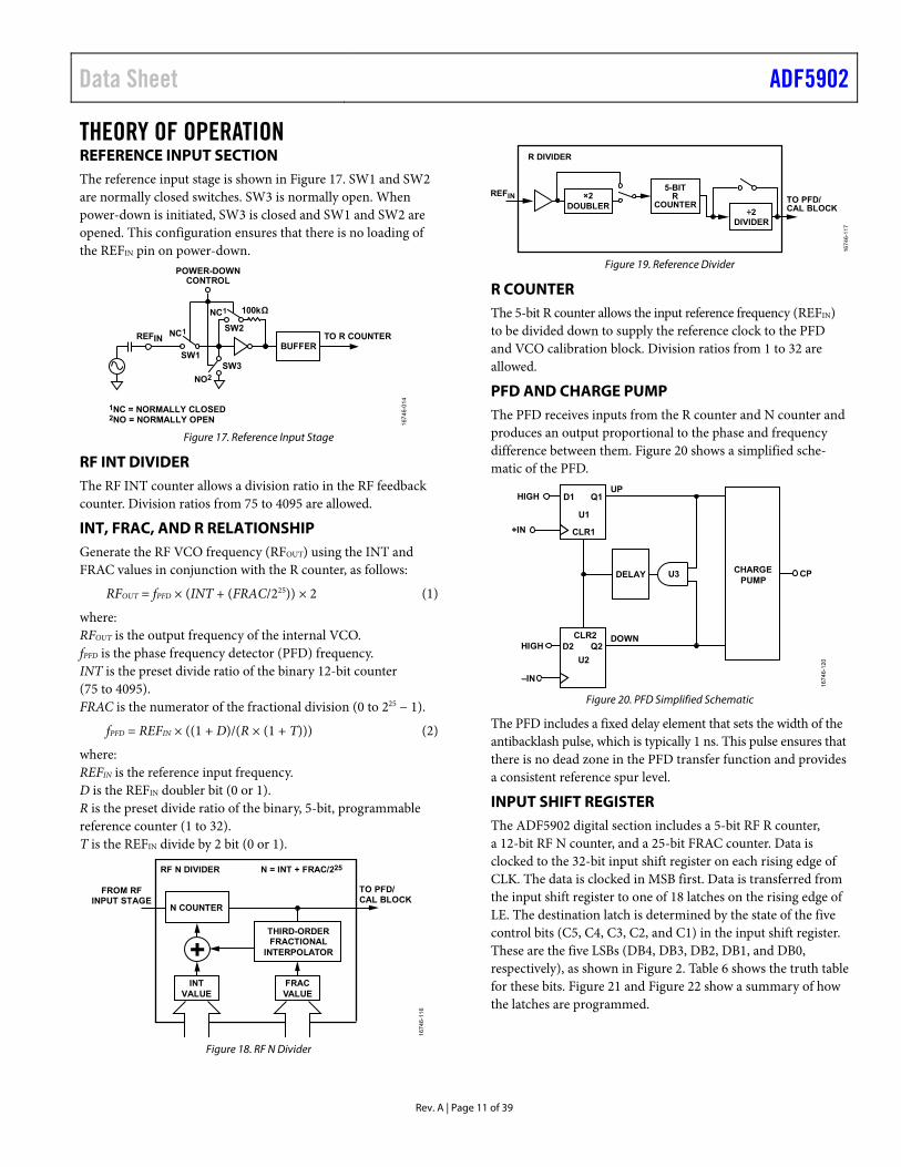
THEORY OF OPERATION REFERENCE INPUT SECTION The reference input stage is shown in Figure 17. SW1 and SW2 are normally closed switches. SW3 is normally open. When power-down is initiated, SW3 is closed and SW1 and SW2 are opened. This configuration ensures that there is no loading of the REFIN pin on power-down.
BUFFERTO R COUNTERREFIN
100kΩNC1
SW2
SW3
NO2
NC1
1NC = NORMALLY CLOSED2NO = NORMALLY OPEN
SW1
POWER-DOWNCONTROL
167
46
-01
4
Figure 17. Reference Input Stage
RF INT DIVIDER The RF INT counter allows a division ratio in the RF feedback counter. Division ratios from 75 to 4095 are allowed.
INT, FRAC, AND R RELATIONSHIP Generate the RF VCO frequency (RFOUT) using the INT and FRAC values in conjunction with the R counter, as follows:
RFOUT = fPFD × (INT + (FRAC/225)) × 2 (1)
where: RFOUT is the output frequency of the internal VCO. fPFD is the phase frequency detector (PFD) frequency. INT is the preset divide ratio of the binary 12-bit counter (75 to 4095). FRAC is the numerator of the fractional division (0 to 225 − 1).
fPFD = REFIN × ((1 + D)/(R × (1 + T))) (2)
where: REFIN is the reference input frequency. D is the REFIN doubler bit (0 or 1). R is the preset divide ratio of the binary, 5-bit, programmable reference counter (1 to 32). T is the REFIN divide by 2 bit (0 or 1).
THIRD-ORDERFRACTIONAL
INTERPOLATOR
FRACVALUE
INTVALUE
RF N DIVIDER N = INT + FRAC/225
FROM RFINPUT STAGE
TO PFD/CAL BLOCK
N COUNTER
1674
6-1
16
Figure 18. RF N Divider
×2DOUBLER
5-BITR
COUNTER÷2
DIVIDER
TO PFD/CAL BLOCK
REFIN
R DIVIDER
1674
6-11
7
Figure 19. Reference Divider
R COUNTER The 5-bit R counter allows the input reference frequency (REFIN) to be divided down to supply the reference clock to the PFD and VCO calibration block. Division ratios from 1 to 32 are allowed.
PFD AND CHARGE PUMP The PFD receives inputs from the R counter and N counter and produces an output proportional to the phase and frequency difference between them. Figure 20 shows a simplified sche-matic of the PFD.
U3
CLR2Q2D2
U2
DOWN
UPHIGH
HIGH
CP
–IN
+IN
CHARGEPUMP
DELAY
CLR1
Q1D1
U1
1674
6-1
20
Figure 20. PFD Simplified Schematic
The PFD includes a fixed delay element that sets the width of the antibacklash pulse, which is typically 1 ns. This pulse ensures that there is no dead zone in the PFD transfer function and provides a consistent reference spur level.
INPUT SHIFT REGISTER The ADF5902 digital section includes a 5-bit RF R counter, a 12-bit RF N counter, and a 25-bit FRAC counter. Data is clocked to the 32-bit input shift register on each rising edge of CLK. The data is clocked in MSB first. Data is transferred from the input shift register to one of 18 latches on the rising edge of LE. The destination latch is determined by the state of the five control bits (C5, C4, C3, C2, and C1) in the input shift register. These are the five LSBs (DB4, DB3, DB2, DB1, and DB0, respectively), as shown in Figure 2. Table 6 shows the truth table for these bits. Figure 21 and Figure 22 show a summary of how the latches are programmed.

ADF5902 Data Sheet
Rev. A | Page 12 of 39
PROGRAM MODES Table 6 and Figure 24 through Figure 42 show how to set up the program modes in the ADF5902.
Several settings in the ADF5902 are double buffered. These include the LSB fractional value, R counter value (R divider), reference doubler, clock divider, RDIV2, and MUXOUT. This means that two events must occur before the device uses a new value for any of the double buffered settings. First, the new value is latched into the device by writing to the appropriate register. Second, a new write must be performed on Register R5.
For example, updating the fractional value can involve a write to the 13 LSB bits in Register R6 and the 12 MSB bits in Register R5. Write to Register R6 first, followed by the write to Register R5. The frequency change begins after the write to Register R5. Double buffering ensures that the bits written to in Register R6 do not take effect until after the write to Register R5.
Table 6. C5, C4, C3, C2, and C1 Truth Table Control Bits
C5 (DB4) C4 (DB3) C3 (DB2) C2 (DB1) C1 (DB0) Register 0 0 0 0 0 R0 0 0 0 0 1 R1 0 0 0 1 0 R2 0 0 0 1 1 R3 0 0 1 0 0 R4 0 0 1 0 1 R5 0 0 1 1 0 R6 0 0 1 1 1 R7 0 1 0 0 0 R8 0 1 0 0 1 R9 0 1 0 1 0 R10 0 1 0 1 1 R11 0 1 1 0 0 R12 0 1 1 0 1 R13 0 1 1 1 0 R14 0 1 1 1 1 R15 1 0 0 0 0 R16 1 0 0 0 1 R17

Data Sheet ADF5902
Rev. A | Page 13 of 39
REGISTER MAPS
1DBR = DOUBLE BUFFERED REGISTER—BUFFERED BY THE WRITE TO REGISTER 5.
REGISTER 0 (R0)
REGISTER 1 (R1)
REGISTER 3 (R3)
REGISTER 4 (R4)
REGISTER 2 (R2)
REGISTER 5 (R5)
REGISTER 6 (R6)
DB31 DB30 DB29 DB28 DB27 DB26 DB25 DB24 DB23 DB22 DB21 DB20 DB19 DB18 DB17 DB16 DB15 DB14 DB13 DB12 DB11 DB10 DB9 DB8 DB7 DB6 DB5 DB4 DB3 DB2 DB1 DB0
1 0 0 0 0 0 0 0
CONTROLBITS
0 0 0 0 1 1 1 1 1 1 1 Tx2C Tx1C PVCO VCAL PADC PTx2 PTx1 PLO C4(0) C3(0) C2(0) C1(0)C5(0)
PU
P L
O
PU
P T
x1
PU
P T
x2
PU
P A
DC
VC
O C
AL
PU
P V
CO
Tx1
AM
P C
AL
Tx2
AM
P C
AL
RESERVED
DB31 DB30 DB29 DB28 DB27 DB26 DB25 DB24 DB23 DB22 DB21 DB20 DB19 DB18 DB17 DB16 DB15 DB14 DB13 DB12 DB11 DB10 DB9 DB8 DB7 DB6 DB5 DB4 DB3 DB2 DB1 DB0
1 1 1 1 1 1 1 1
CONTROLBITS
1 1 1 1 0 1 1 1 1 1 1 C4(0) C3(0) C2(0) C1(1)
Tx AMP CAL REF CODE
C5(0)TAR7 TAR6 TAR5 TAR4 TAR3 TAR2 TAR1 TAR0
DB31 DB30 DB29 DB28 DB27 DB26 DB25 DB24 DB23 DB22 DB21 DB20 DB19 DB18 DB17 DB16 DB15 DB14 DB13 DB12 DB11 DB10 DB9 DB8 DB7 DB6 DB5 DB4 DB3 DB2 DB1 DB0
0 0 0 0 0 0 0 0 0
CONTROLBITS
0 0 0 0 0 1 0 AS AA0 AA0 AC7 AC6 AC5 AC4 AC3 AC2 AC1 AC0 C4(0) C3(0) C2(1) C1(0)
RESERVED ADC CLOCK DIVIDERADC
AVERAGEAD
C S
TA
RT
C5(0)
DB31 DB30 DB29 DB28 DB27 DB26 DB25 DB24 DB23 DB22 DB21 DB20 DB19 DB18 DB17 DB16 DB15 DB14 DB13 DB12 DB11 DB10 DB9 DB8 DB7 DB6 DB5 DB4 DB3 DB2 DB1 DB0
0 0 0 0 0 0 0 1 1 0 0 0 1 0 0 1 M3 M2 M1 M0 IOL RC5 RC4 RC3 RC2 RC1 RC0 C4(0) C3(0) C2(1) C1(1)
CONTROLBITSMUXOUT DBR1RESERVED
C5(0)
READBACK CONTROLIO L
EV
EL
DB31 DB30 DB29 DB28 DB27 DB26 DB25 DB24 DB23 DB22 DB21 DB20 DB19 DB18 DB17 DB16 DB15 DB14 DB13 DB12 DB11 DB10 DB9 DB8 DB7 DB6 DB5 DB4 DB3 DB2 DB1 DB0
0 0 0 0 0 0 0 0 AB9AB14 AB13 AB12 AB11 AB10 AB8 AB7 AB6 AB5 AB4 AB3 AB2 AB1 AB0 C4(0) C3(1) C2(0) C1(0)
CONTROLBITSRESERVED
0 0 0 0
RAMP STATUS/ANALOG TEST BUS
C5(0)
DB31 DB30 DB29 DB28 DB27 DB26 DB25 DB24 DB23 DB22 DB21 DB20 DB19 DB18 DB17 DB16 DB15 DB14 DB13 DB12 DB11 DB10 DB9 DB8 DB7 DB6 DB5 DB4 DB3 DB2 DB1 DB0
0 0 N11RON N10 N9 N8 N7 N6 N5 N4 N3 N2 N1 N0 F24 F23 F22 F21 F20 F19 F18 F17 F16 F15 F14 F13 C4(0) C3(1) C2(0) C1(1)
CONTROLBITS
RESERVED RA
MP
ON
FRAC MSB WORDINTEGER WORD
C5(0)
DB31 DB30 DB29 DB28 DB27 DB26 DB25 DB24 DB23 DB22 DB21 DB20 DB19 DB18 DB17 DB16 DB15 DB14 DB13 DB12 DB11 DB10 DB9 DB8 DB7 DB6 DB5 DB4 DB3 DB2 DB1 DB0
0 0 0 0 0 0 0 0 0 0 0 0 0 0 F12 F11 F10 F9 F8 F7 F6 F5 F4 F3 F2 F1 F0 C4(0) C3(1) C2(1) C1(0)
CONTROLBITS
FRAC LSB WORD
C5(0)
DBR1RESERVED
RESERVED
1674
6-0
17
Figure 21. Register Summary (Register 0 to Register 6)

ADF5902 Data Sheet
Rev. A | Page 14 of 39
REGISTER 7 (R7)
REGISTER 8 (R8)
REGISTER 10 (R10)
REGISTER 9 (R9)
DB31 DB30 DB29 DB28 DB27 DB26 DB25 DB24 DB23 DB22 DB21 DB20 DB19 DB18 DB17 DB16 DB15 DB14 DB13 DB12 DB11 DB10 DB9 DB8 DB7 DB6 DB5 DB4 DB3 DB2 DB1 DB0
0 0 0 0 0 0 MR 1
CONTROLBITS
RD2 RD R4 R3 R2 R1 R0 C4(0) C3(1) C2(1) C1(1)C5(0)
RE
F D
OU
BL
ER
DB
R1
RD
IV2
D
BR
1
RESERVED MA
ST
ER
RE
SE
TR DIVIDER DBR1
DB31 DB30 DB29 DB28 DB27 DB26 DB25 DB24 DB23 DB22 DB21 DB20 DB19 DB18 DB17 DB16 DB15 DB14 DB13 DB12 DB11 DB10 DB9 DB8 DB7 DB6 DB5 DB4 DB3 DB2 DB1 DB0
0 1 0 0 0 0 0 0
CONTROLBITS
0 0 0 0 0 0 0 0 0 FC9 FC8 FC7 FC6 FC5 FC4 FC3 FC2 FC1 FC0 C4(1) C3(0) C2(0) C1(0)
FREQENCY CAL DIVIDER
C5(0)
RESERVED
DB31 DB30 DB29 DB28 DB27 DB26 DB25 DB24 DB23 DB22 DB21 DB20 DB19 DB18 DB17 DB16 DB15 DB14 DB13 DB12 DB11 DB10 DB9 DB8 DB7 DB6 DB5 DB4 DB3 DB2 DB1 DB0
0 0 1 0 1 0 1 0 0
CONTROLBITS
0 1 0 0 0 0 0 1 0 1 1 1 0 0 1 0 0 1 C4(1) C3(0) C2(0) C1(1)C5(0)
RESERVED
DB31 DB30 DB29 DB28 DB27 DB26 DB25 DB24 DB23 DB22 DB21 DB20 DB19 DB18 DB17 DB16 DB15 DB14 DB13 DB12 DB11 DB10 DB9 DB8 DB7 DB6 DB5 DB4 DB3 DB2 DB1 DB0
0 0 0 1 1 1 0 1 0 0 1 1 0 0 1 0 1 0 1 0 0 1 1 0 0 1 0 C4(1) C3(0) C2(1) C1(0)
CONTROLBITSRESERVED
C5(0)
CLOCK DIVIDER
C1D11C1D10 C1D9 C1D8 C1D7 C1D6 C1D5 C1D4 C1D3 C1D2 C1D1 C1D0
DBR1
RE
SE
RV
ED
DB31 DB30 DB29 DB28 DB27 DB26 DB25 DB24 DB23 DB22 DB21 DB20 DB19 DB18 DB17 DB16 DB15 DB14 DB13 DB12 DB11 DB10 DB9 DB8 DB7 DB6 DB5 DB4 DB3 DB2 DB1 DB0
0 0 0 0 0 0 0 0 0 0 0 0 0 0 0 0 0 0 0 0 SDR 0 SFT RM1
RAMPMODE
RM0 0 CR C4(1) C3(0) C2(1) C1(1)
CONTROLBITSRESERVED
C5(0)
REGISTER 11 (R11)
CN
TR
RE
SE
T
SD
RE
SE
T
RE
SE
RV
ED
RE
SE
RV
ED
SIN
G F
UL
LT
RI
RA
MP
16
746
-018
1DBR = DOUBLE BUFFERED REGISTER—BUFFERED BY THE WRITE TO REGISTER 5.
DB31 DB30 DB29 DB28 DB27 DB26 DB25 DB24 DB23 DB22 DB21 DB20 DB19 DB18 DB17 DB16 DB15 DB14 DB13 DB12 DB11 DB10 DB9 DB8 DB7 DB6 DB5 DB4 DB3 DB2 DB1 DB0
0 0 0 0 0 0 0 1 0 1 C4(1) C3(1) C2(0) C1(0)
CONTROLBITS
C5(0)
REGISTER 12 (R12)
CHARGE PUMPCURRENT
CC3 CC2 CC1 CC0
CP
TR
IST
AT
ED
BR
1
CTRI
RE
SE
RV
ED
0 0 0 0 0 0 0 0 0 0
RESERVED
0 0
DBR1
RESERVED
Figure 22. Register Summary (Register 7 to Register 12)

Data Sheet ADF5902
Rev. A | Page 15 of 39
REGISTER 13 (R13)
DB31 DB30 DB29 DB28 DB27 DB26 DB25 DB24 DB23 DB22 DB21 DB20 DB19 DB18 DB17 DB16 DB15 DB14 DB13 DB12 DB11 DB10 DB9 DB8 DB7 DB6 DB5 DB4 DB3 DB2 DB1 DB0
0 0 0 0 0 0 0 0 0 0 LES CDM1 CDM0 C2D11C2D10 C2D9 C2D8 C2D7 C2D6 C2D5 C2D4 C2D3 C2D2 C2D1 C2D0 CDS1 CDS0 C4(1) C3(1) C2(0) C1(1)
CONTROLBITS
CLOCK DIVIDER 2
C5(0)
RESERVED CL
K D
IVS
EL
CL
K D
IVM
OD
E
LE
SE
LDB31 DB30 DB29 DB28 DB27 DB26 DB25 DB24 DB23 DB22 DB21 DB20 DB19 DB18 DB17 DB16 DB15 DB14 DB13 DB12 DB11 DB10 DB9 DB8 DB7 DB6 DB5 DB4 DB3 DB2 DB1 DB0
TDI TRC 0 0 DS1 DS0 DO3
CONTROLBITS
DO2 DO1 DO0 DW15 DW14 DW13 DW12 DW11 DW10 DW9 DW8 DW7 DW6 DW5 DW4 DW3 DW2 DW1 DW0 C4(1) C3(1) C2(1) C1(0)
DB31 DB30 DB29 DB28 DB27 DB26 DB25 DB24 DB23 DB22 DB21 DB20 DB19 DB18 DB17 DB16 DB15 DB14 DB13 DB12 DB11 DB10 DB9 DB8 DB7 DB6 DB5 DB4 DB3 DB2 DB1 DB0
0 SS1 SS0 SW19
CONTROLBITS
SW18 SW17 SW16 SW15 SW14 SW13 SW12 SW11 SW10 SW9 SW8 SW7 SW6 SW5 SW4 SW3 SW2 SW1 SW0 C4(1) C3(1) C2(1) C1(1)
REGISTER 14 (R14)
REGISTER 15 (R15)
DB31 DB30 DB29 DB28 DB27 DB26 DB25 DB24 DB23 DB22 DB21 DB20 DB19 DB18 DB17 DB16 DB15 DB14 DB13 DB12 DB11 DB10 DB9 DB8 DB7 DB6 DB5 DB4 DB3 DB2 DB1 DB0
0 0 0 0 0 0 DSL1 DSL0
CONTROLBITS
TR1 RD DS11 DS10 DS9 DS8 DS7 DS6 DS5 DS4 DS3 DS2 DS1 DS0 C4(0) C3(0) C2(0) C1(0)
REGISTER 16 (R16)
C5(0)
STEP WORD
DELAY START WORD
C5(0)
RE
SE
RV
ED
C5(1)
DEVIATION WORDDEVIATION OFFSETDEVIATION
SELTX
RA
MP
CL
K
Tx_
DA
TA
IN
V
STEPSEL
RA
MP
DE
L
Tx_
DA
TA
TR
IGG
ER
RESERVEDDELAYSELECT
0 0 0 0
RESERVED
RESERVED
0
RE
SE
RV
ED
0
DB31 DB30 DB29 DB28 DB27 DB26 DB25 DB24 DB23 DB22 DB21 DB20 DB19 DB18 DB17 DB16 DB15 DB14 DB13 DB12 DB11 DB10 DB9 DB8 DB7 DB6 DB5 DB4 DB3 DB2 DB1 DB0
0 0 0 0 0 0 0 0 0
CONTROLBITS
0 0 0 0 0 0 0 0 0 0 0 0 0 0 0 0 0 C4(0) C3(0) C2(0) C1(1)
REGISTER 17 (R17)
C5(1)
RESERVED
0
0 0 01
16
746
-121
Figure 23. Register Summary (Register 13 to Register 17)

ADF5902 Data Sheet
Rev. A | Page 16 of 39
DB31 DB30 DB29 DB28 DB27 DB26 DB25 DB24 DB23 DB22 DB21 DB20 DB19 DB18 DB17 DB16 DB15 DB14 DB13 DB12 DB11 DB10 DB9 DB8 DB7 DB6 DB5 DB4 DB3 DB2 DB1 DB0
1 0 0 0 0 0 0 0 0 0 0 0
CONTROLBITS
1 1 1 1 1 1 1 Tx2C Tx1C PVCO VCAL PADC PTx2 PTx1 PLO C4(0) C3(0) C2(0) C1(0)C5(0)
PU
P L
O
PU
P T
x1
PU
P T
x2
PU
P A
DC
VC
O C
AL
PU
P V
CO
Tx1
AM
P C
AL
Tx2
AM
P C
AL
RESERVED
PLO
0
1
PUP LO
POWER UP LO
POWER DOWN LO
PTx1
0
1
PUP Tx1
POWER UP Tx1
POWER DOWN Tx1
PTx2
0
1
PUP Tx2
POWER UP Tx2
POWER DOWN Tx2
PADC
0
1
PUP ADC
POWER UP ADC
POWER DOWN ADC
VCAL
0
1
VCO CAL
VCO FULL CAL
NORMAL OPERATION
PVCO
0
1
PUP VCO
POWER UP VCO
POWER DOWN VCO
Tx1C
0
1
Tx1 AMP CAL
Tx1 AMP CAL
NORMAL OPERATION
Tx2C
0
1
Tx2 AMP CAL
Tx2 AMP CAL
NORMAL OPERATION
16
74
6-0
19
Figure 24. Register 0 (R0)
REGISTER 0 Control Bits With Bits[C5:C1] set to 00000, Register R0 is programmed. Figure 24 shows the input data format for programming this register.
Reserved Bits[DB31:DB13] are reserved and must be set as shown in Figure 24.
Transmitter 2 (Tx2) Amplitude Calibration Bit DB12 provides the control bit for amplitude calibration of the Tx2 output. Set this bit to 0 for normal operation. Setting this bit to 1 performs an amplitude calibration of the Tx2 output. Bit DB12 is shown as Tx2 AMP CAL in Figure 24.
Tx1 Amplitude Calibration Bit DB11 provides the control bit for amplitude calibration of the Tx1 output. Set this bit to 0 for normal operation. Setting this bit to 1 performs an amplitude calibration of the Tx1 output. Bit DB11 is shown as Tx1 AMP CAL in Figure 24.
Power-Up VCO Bit DB10 provides the power-up bit for the VCO. Setting this bit to 0 performs a power-down of the VCO. Setting this bit to 1 performs a power-up of the VCO. Bit DB10 is shown as PUP VCO in Figure 24.
VCO Calibration Bit DB9 provides the control bit for frequency calibration of the VCO. Set this bit to 0 for normal operation. Setting this bit to 1 performs a VCO frequency and amplitude calibration. Bit DB9 is shown as VCO CAL in Figure 24.
Power-Up ADC Bit DB8 provides the power-up bit for the ADC. Setting this bit to 0 performs a power-down of the ADC. Setting this bit to 1 performs a power-up of the ADC. Bit DB8 is shown as PUP ADC in Figure 24.
Power-Up Tx2 Output Bit DB7 provides the power-up bit for the Tx2 output. Setting this bit to 0 performs a power-down of the Tx2 output. Setting this bit to 1 performs a power-up of the Tx2 output. Only one transmitter output can be powered up at any time, either Tx1 (DB6) or Tx2 (DB7). Bit DB7 is shown as PUP Tx2 in Figure 24.
Power-Up Tx1 Output Bit DB6 provides the power-up bit for the Tx1 output. Setting this bit to 0 performs a power-down of the Tx1 output. Setting this bit to 1 performs a power-up of the Tx1 output. Only one Tx output can be powered up at any time, either Tx1 (DB6) or Tx2 (DB7). Bit DB6 is shown as PUP Tx1 in Figure 24.
Power-Up LO Output Bit DB5 provides the power-up bit for the LO output. Setting this bit to 0 performs a power-down of the LO output. Setting this bit to 1 performs a power-up of the LO output. Bit DB5 is shown as PUP LO in Figure 24.

Data Sheet ADF5902
Rev. A | Page 17 of 39
DB31 DB30 DB29 DB28 DB27 DB26 DB25 DB24 DB23 DB22 DB21 DB20 DB19 DB18 DB17 DB16 DB15 DB14 DB13 DB12 DB11 DB10 DB9 DB8 DB7 DB6 DB5 DB4 DB3 DB2 DB1 DB0
1 1 1 1 1 1 1 1
CONTROLBITS
1 1 1 1 0 1 1 1 1 1 1 C4(0) C3(0) C2(0) C1(1)
Tx AMP CAL REF CODE
C5(0)TAR7 TAR6 TAR5 TAR4 TAR3 TAR2 TAR1 TAR0
TAR7 TAR6 .......... TAR1 TAR0
0 0 .......... 0 0 0
0 0 .......... 0 1 1
0 0 .......... 1 0 2
0 0 .......... 1 1 3
. . .......... . . .
. . .......... . . .
. . .......... . . .
1 1 .......... 0 0 252
1 1 .......... 0 1 253
1 1 .......... 1 0 254
1 1 ......... 1 1 255
Tx AMP CAL REF CODE
RESERVED
16
746
-02
0
Figure 25. Register 1 (R1)
REGISTER 1 Control Bits
With Bits[C5:C1] set to 00001, Register R1 is programmed. Figure 25 shows the input data format for programming this register.
Reserved
Bits[DB31:DB13] are reserved and must be set as shown in Figure 25.
Transmitter Amplitude Calibration Reference Code
Bits[DB12:DB5] set the transmitter amplitude calibration reference code for the two transmitter outputs during calibration. Calibrate the output power on the transmitter outputs from −20 dBm to 8 dBm by setting the transmitter amplitude calibration reference code (see Figure 7). Bits[DB12:DB5] are shown as Tx AMP CAL REF CODE in Figure 25.

ADF5902 Data Sheet
Rev. A | Page 18 of 39
DB31 DB30 DB29 DB28 DB27 DB26 DB25 DB24 DB23 DB22 DB21 DB20 DB19 DB18 DB17 DB16 DB15 DB14 DB13 DB12 DB11 DB10 DB9 DB8 DB7 DB6 DB5 DB4 DB3 DB2 DB1 DB0
0 0 0 0 0 0 0 0 0
CONTROLBITS
0 0 0 0 0 1 0 AS AA0 AA0 AC7 AC6 AC5 AC4 AC3 AC2 AC1 AC0 C4(0) C3(0) C2(1) C1(0)
RESERVED ADC CLOCK DIVIDERADC
AVERAGEAD
C S
TA
RT
C5(0)
AC7 AC6 AC1 AC0 ADC CLOCK DIVIDER
0 0 0 1 1
0 0 1 0 2
. . . . .
. . . . .
. . . . .
1 1 0 0 124
1 1 0 1 125
1 1 1 0 126
1 1 1 1 127
.
.
.
.
.
.
.
.
.
.
AS
0
1
ADC START
START ADC CONVERSION
NORMAL OPERATION
AA1 AA0 ADC AVERAGE
0 0 1
0 1 2
1 0 3
1 1 4
1674
6-02
1
Figure 26. Register 2 (R2)
REGISTER 2 Control Bits
With Bits[C5:C1] set to 00010, Register R2 is programmed. Figure 26 shows the input data format for programming this register.
Reserved
Bits[DB31:DB16] are reserved and must be set as shown in Figure 26.
ADC Start
Bit DB15 starts the ADC conversion. Setting this bit to 1 starts an ADC conversion.
ADC Average
Bits[DB14:DB13] program the ADC average, which is the number of averages of the ADC output (see Figure 26).
ADC Clock Divider
Bits[DB12:DB5] program the clock divider, which is used as the sampling clock for the ADC (see Figure 26). The output of the R divider block clocks the ADC clock divider. Program a divider value to ensure the ADC sampling clock is 1 MHz.
Data Sheet ADF5902
Rev. A | Page 19 of 39
DB31 DB30 DB29 DB28 DB27 DB26 DB25 DB24 DB23 DB22 DB21 DB20 DB19 DB18 DB17 DB16 DB15 DB14 DB13 DB12 DB11 DB10 DB9 DB8 DB7 DB6 DB5 DB4 DB3 DB2 DB1 DB0
0 0 0 0 0 0 0 1 1 0 0 0 1 0 0 1 M3 M2 M1 M0 IOL RC5 RC4 RC3 RC2 RC1 RC0 C4(0) C3(0) C2(1) C1(1)
CONTROLBITSRESERVED
C5(0)
READBACK CONTROLIO L
EV
EL
M3 M2 M1 M0 MUXOUT
0 0 0 0 TRISTATE OUTPUT
0 0 0 1 LOGIC HIGH
0 0 1 0 LOGIC LOW
0 0 1 1 R DIVIDER OUTPUT
0 1 0 0 N DIVIDER OUTPUT
0 1 0 1 RESERVED
0 1 1 0 RESERVED
0 1 1 1 CAL BUSY
1 0 0 0 RESERVED
1 0 0 1 RESERVED
1 0 1 0 RESERVED
1 0 1 1 R DIVIDER/2
1 1 0 0 N DIVIDER/2
1 1 0 1 RESERVED
1 1 1 0 RESERVED
1 1 1 1 RAMP STATUS TO MUXOIUT
IOL
0
1
IO LEVEL
3.3V LOGIC OUTPUTS
1.8V LOGIC OUTPUTS
1DBR = DOUBLE-BUFFERED REGISTER.
MUXOUT DBR1
16
746
-02
2
RC3 RC2 RC1 RC0 READBACK CONTROL
0 0 0 0 NONE
0 0 0 1 REGISTER 0
0 0 1 0 REGISTER 1
0 0 1 1 REGISTER 2
0 1 0 0 REGISTER 3
0 1 0 1 REGISTER 4
0 1 1 0 REGSITER 5
0 1 1 1 REGISTER 6
1 0 0 0 REGISTER 7
1 0 0 1 REGISTER 8
1 0 1 0 REGISTER 9
1 0 1 1 REGISTER 10
REGISTER 111 1 0 0
. . . . RESERVED
0 1 1 0 ADC READBACK
RC4
0
0
0
0
0
0
0
0
0
0
0
0
0
.
1
. . . ..
RC5
0
0
0
0
0
0
0
0
0
0
0
0
0
.
0
.
1 1 0 1 REGISTER 12
REGISTER 13 SEL = 01 1 1 00
0
0
01 1 1 1
0 0 0 00
1
0
0
0 0 0 1REGISTER 170 0 1 0
1
1
0
0
REGISTER 13 SEL = 1
REGISTER 14 SEL = 0
REGISTER 15 SEL = 0
REGISTER 16 SEL = 0
REGISTER 14 SEL = 1
REGISTER 15 SEL = 1
REGISTER 16 SEL = 1
REGISTER 13 SEL = 2
REGISTER 14 SEL = 2
REGISTER 15 SEL = 2
REGISTER 16 SEL = 2
REGISTER 13 SEL = 3
REGISTER 14 SEL = 3
REGISTER 15 SEL = 3
REGISTER 16 SEL = 3
1
0
1
0
1
0
1
0
10
1
0
1
1
0
0
1
1
0
0
1
10
0
1
1
1
1
1
1
0
0
0
01
1
1
1
00
0
0
0
0
1
11
1
1
1
1
1
1
11
1
1
1
1
1
1
11
1
1
1
1
1
1
11
1
1
1
11
1
1
01 1 01
. . . ..
0
. RESERVED
FREQ READBACK
RESERVED
RESERVED
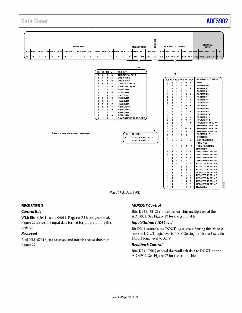
Figure 27. Register 3 (R3)
REGISTER 3 Control Bits
With Bits[C5:C1] set to 00011, Register R3 is programmed. Figure 27 shows the input data format for programming this register.
Reserved
Bits[DB31:DB16] are reserved and must be set as shown in Figure 27.
MUXOUT Control
Bits[DB15:DB12] control the on-chip multiplexer of the ADF5902. See Figure 27 for the truth table.
Input/Output (I/O) Level
Bit DB11 controls the DOUT logic levels. Setting this bit to 0 sets the DOUT logic level to 1.8 V. Setting this bit to 1 sets the DOUT logic level to 3.3 V.
Readback Control
Bits[DB10:DB5] control the readback data to DOUT on the ADF5902. See Figure 27 for the truth table.

ADF5902 Data Sheet
Rev. A | Page 20 of 39
DB31 DB30 DB29 DB28 DB27 DB26 DB25 DB24 DB23 DB22 DB21 DB20 DB19 DB18 DB17 DB16 DB15 DB14 DB13 DB12 DB11 DB10 DB9 DB8 DB7 DB6 DB5 DB4 DB3 DB2 DB1 DB0
0 0 0 0 0 0 0 0 AB9 AB8 AB7 AB6 AB5 AB4 AB3 AB2 AB1 AB0 C4(0) C3(1) C2(0) C1(0)
CONTROLBITSRESERVED
0 0 0 0 AB14 AB13 AB12 AB11 AB10
RAMP STATUS/ANALOG TEST BUS
C5(0)
167
46-
02
3
AB3 AB2 AB1 AB0
0 0 0 0
0 0 0 0
ANALOG TEST BUSAB7 AB6 AB5 AB4
0 0 0 0
1 1 0 0
AB9 AB8
0 0
0 0
NONE
RAMP COMPLETE TO MUXOUT
0 0 0
0 0 0
0 0
0 0
0 0 0 0
0 0 1 1
0 0 0 0
0 0 0 0
0 1
0 1
RAMP DOWN TO MUXOUT
TEMPERATURE SENSOR TO ATEST
0 0 0
0 0 1
0 0
0 0
0 0 1 10 0 0 00 1 TEMPERATURE SENSOR TO ADC1 0
0x0503
0x0100
0x00C0
0x0903
0x0000
AB11 AB10AB12AB13AB14
000
Figure 28. Register 4 (R4)
REGISTER 4 Control Bits
With Bits[C5:C1] set to 00100, Register R4 is programmed. Figure 28 shows the input data format for programming this register.
Reserved
Bits[DB31:DB20] are reserved and must be set as shown in Figure 28.
Ramp Status/Analog Test Bus
Bits[DB19:DB5] control the analog test bus and the ramp status to MUXOUT (see Figure 28).
The analog test bus allows access to internal test signals for the temperature sensor which can be connected to the ATEST pin or the internal ADC.
Setting Bits DB[19:5] to 0 (no value) sets the ATEST pin to high impedance.
For ramp status outputs on MUXOUT, the MUXOUT bits in Register R3 (Bits[DB15:DB12]) must be set to 1111 to access these modes.

Data Sheet ADF5902
Rev. A | Page 21 of 39
DB31 DB30 DB29 DB28 DB27 DB26 DB25 DB24 DB23 DB22 DB21 DB20 DB19 DB18 DB17 DB16 DB15 DB14 DB13 DB12 DB11 DB10 DB9 DB8 DB7 DB6 DB5 DB4 DB3 DB2 DB1 DB0
0 0 RON N11 N10 N9 N8 N7 N6 N5 N4 N3 N2 N1 N0 F24 F23 F22 F21 F20 F19 F18 F17 F16 F15 F14 F13 C4(0) C3(1) C2(0) C1(1)
CONTROLBITS
RESERVED RA
MP
ON
FRAC MSB WORDINTEGER WORD
C5(0)
N11 N10 ... N4 N3 N2 N1 N0
0 0 ... 0 0 0 0 0 NOT ALLOWED
0 0 ... 0 0 0 0 1 NOT ALLOWED
0 0 ... 0 0 0 1 0 NOT ALLOWED
. . ... . . . . . ...
0 0 ... 0 1 0 1 0 NOT ALLOWED
0 0 ... 0 1 0 1 1 75
0 0 ... 0 1 1 0 0 76
. . ... . . . . . ...
1 1 ... 1 1 1 0 1 4093
1 1 ... 1 1 1 1 0 4094
1 1 ... 1 1 1 1 1 4095
F24 F23 .......... F14 F13 (FRAC)*
0 0 .......... 0 0 0
0 0 .......... 0 1 1
0 0 .......... 1 0 2
0 0 .......... 1 1 3
. . .......... . . .
. . .......... . . .
. . .......... . . .
1 1 .......... 0 0 4092
1 1 .......... 0 1 4093
1 1 .......... 1 0 4094
1 1 ......... 1 1 4095
*THE FRAC VALUE IS MADE UP OF THE 12-BIT MSB STORED IN REGISTER R5, AND THE 13-BIT LSB REGISTER STORED IN REGISTER R6. FRAC VALUE = 13-BIT LSB + 12-BIT MSB × 213.
INTEGER WORD FRAC MSB WORD
1674
6-02
4R1 RAMP ON
0 RAMP DISABLED
RAMP ENABLED1
Figure 29. Register 5 (R5)
REGISTER 5 Control Bits
With Bits[C5:C1] set to 00101, Register R5 is programmed. Figure 29 shows the input data format for programming this register.
Reserved
Bits[DB31:DB30] are reserved and must be set as shown in Figure 29.
Ramp On
When Bit DB29 is set to 1, the ramp is started. When Bit DB29 is set to 0, the ramp function is disabled.
In continuous ramp modes, the ramp stops when Bit DB29 is set to 0. For applications that require the ramp to stop at the initial frequency, a write to Register R6 is required prior to disabling the ramp function. In single ramp modes, a write to Register R6 is required prior to repeating the single ramp function.
When using the TX_DATA pin to trigger the ramp off in continuous ramp modes, the ramp stops at the initial frequency, a write to Register R6 is not required. When using the TX_ DATA pin in single ramp modes, a write to Register R6 is not required prior to repeating the single ramp function.
12-Bit Integer Value (INT)
These 12 bits (Bits[DB28:DB17]) set the INT value, which determines the integer part of the RF division factor. This INT value is used in Equation 5. See the RF Synthesis: A Worked Example section for more information. All integer values from 75 to 4095 are allowed.
12-Bit MSB Fractional Value (FRAC)
Bits[DB16:DB5], together with Bits[DB17:DB5] (FRAC LSB word) in Register R6, control what is loaded as the FRAC value into the fractional interpolator. This FRAC value partially determines the overall RF division factor. It is also used in Equation 1. These 12 bits are the most significant bits (MSB) of the 25-bit FRAC value, and Bits[DB17:DB5] (FRAC LSB word) in Register R6 are the least significant bits (LSB). See the RF Synthesis: A Worked Example section for more information.

ADF5902 Data Sheet
Rev. A | Page 22 of 39
DB31 DB30 DB29 DB28 DB27 DB26 DB25 DB24 DB23 DB22 DB21 DB20 DB19 DB18 DB17 DB16 DB15 DB14 DB13 DB12 DB11 DB10 DB9 DB8 DB7 DB6 DB5 DB4 DB3 DB2 DB1 DB0
0 0 0 0 0 0 0 0 0 0 0 0 0 F12 F11 F10 F9 F8 F7 F6 F5 F4 F3 F2 F1 F0 C4(0) C3(1) C2(1) C1(0)
CONTROLBITS
FRAC LSB WORD
C5(0)
F12 F11 .......... F1 F0 (FRAC)*
0 0 .......... 0 0 0
0 0 .......... 0 1 1
0 0 .......... 1 0 2
0 0 .......... 1 1 3
. . .......... . . .
. . .......... . . .
. . .......... . . .
1 1 .......... 0 0 8188
1 1 .......... 0 1 8189
1 1 .......... 1 0 8190
1 1 ......... 1 1 8191
1DBR = DOUBLE-BUFFERED REGISTER.
*THE FRAC VALUE IS MADE UP OF THE 12-BIT MSB STORED IN REGISTER R5, AND THE 13-BIT LSB REGISTER STORED IN REGISTER R6. FRAC VALUE = 13-BIT LSB + 12-BIT MSB × 213.
FRAC LSB WORD
DBR1RESERVED
167
46
-02
5
Figure 30. Register 6 (R6)
REGISTER 6 Control Bits
With Bits[C5:C1] set to 00110, Register R6 is programmed. Figure 30 shows the input data format for programming this register.
Reserved
Bits[DB31:DB18] are reserved and must be set as shown in Figure 30.
13-Bit LSB FRAC Value
These 13 bits (Bits[DB17:DB5]), together with Bits[DB16:DB5] (FRAC MSB word) in Register R5, control what is loaded as the FRAC value into the fractional interpolator. This FRAC value partially determines the overall RF division factor. It is also used in Equation 1. These 13 bits are the least significant bits (LSB) of the 25-bit FRAC value, and Bits[DB16:DB5] (FRAC MSB word) in Register R5 are the most significant bits (MSB). See the RF Synthesis: A Worked Example section for more information.

Data Sheet ADF5902
Rev. A | Page 23 of 39
DB31 DB30 DB29 DB28 DB27 DB26 DB25 DB24 DB23 DB22 DB21 DB20 DB19 DB18 DB17 DB16 DB15 DB14 DB13 DB12 DB11 DB10 DB9 DB8 DB7 DB6 DB5 DB4 DB3 DB2 DB1 DB0
0 0 0 0 0 0 MR 1
CONTROLBITS
RD2 RD R4 R3 R2 R1 R0 C4(0) C3(1) C2(1) C1(1)C5(0)
RE
F D
OU
BL
ER
RD
IV2
RESERVED MA
ST
ER
RE
SE
T
R DIVIDER
R4 R3 R1 R0 R DIVIDER (R)
0 0 0 1 1
0 0 1 0 2
. . . . .
. . . . .
. . . . .
1 1 0 0 28
1 1 0 1 29
1 1 1 0 30
1 1 1 1 31
RD
0 DISABLED
1 ENABLED
RD2
0 DISABLED
1 ENABLED
R2
0
0
.
.
.
1
1
1
1
REFDOUBLER
RDIV2MR
0
1
MASTER RESET
ENABLED
DISABLED
DBRDB
R1
DB
R1
CLOCK DIVIDER
C1D11 C1D10 .......... C1D2 C1D0
0 0 .......... 0 0 0
0 0 .......... 0 1 1
0 0 .......... 1 0 2
0 0 .......... 1 1 3
. . .......... . . .
. . .......... . . .
. . .......... . . .
1 1 .......... 0 0 4092
1 1 .......... 0 1 4093
1 1 .......... 1 0 4094
1 1 ......... 1 1 4095
C1D11C1D10 C1D9 C1D8 C1D7 C1D6 C1D5 C1D4 C1D3 C1D2 C1D1 C1D0
DBR1
CLOCK DIVIDER (CLK1)
RE
SE
RV
ED
1DBR = DOUBLE-BUFFERED REGISTER.
167
46-
02
6
Figure 31. Register 7 (R7)
REGISTER 7 Control Bits
With Bits[C5:C1] set to 00111, Register R7 is programmed. Figure 31 shows the input data format for programming this register.
Reserved
Bits[DB31:DB26] are reserved and must be set as shown in Figure 31.
Master Reset
Bit DB25 provides a master reset bit for the device. Setting this bit to 1 performs a reset of the device and all register maps. Setting this bit to 0 returns the device to normal operation.
Clock Divider Bits[DB23:DB12] controls the clock divider (CLK1) value (see Figure 31). The CLK1 value sets a divider for the VCO frequency calibration. Load the divider such that PFD frequency (fPFD)/ CLK1 is less than or equal to 25 kHz.
For example, for fPFD = 50 MHz, set CLK1 = 2048 so that fPFD/ CLK1 < 25 kHz.
The CLK1 value is also used to determine the duration of the time step in ramp mode. See the Ramp and Modulation section for more information.
Divide by 2 (RDIV2)
Setting the DB11 bit to 1 inserts a divide by 2 toggle flip flop between the R counter and VCO calibration block.
Reference Doubler
Setting DB10 to 0 feeds the REFIN signal directly to the 5-bit R counter, disabling the doubler. Setting this bit to 1 multiplies the REFIN frequency by a factor of 2 before the REFIN signal is fed to the 5-bit R counter. When the doubler is disabled, the REFIN falling edge is the active edge at the PFD input to the fractional synthesizer. When the doubler is enabled, both the rising and falling edges of REFIN become active edges at the PFD input.
When the reference doubler is enabled, for optimum phase noise performance, it is recommended to only use charge pump current settings of 0b0000 to 0b0111, that is, 0.28 mA to 2.24 mA in Register 12. In this case, the best practice is to design the loop filter for a charge pump current of 1.12 mA or 1.4 mA and then use the programmable charge pump current to adjust the frequency response.
The maximum allowable REFIN frequency when the doubler is enabled is 50 MHz.
5-Bit R Divider
The 5-bit R counter allows the input reference frequency (REFIN) to be divided down to produce the reference clock to the VCO calibration block. Division ratios from 1 to 31 are allowed.

ADF5902 Data Sheet
Rev. A | Page 24 of 39
DB31 DB30 DB29 DB28 DB27 DB26 DB25 DB24 DB23 DB22 DB21 DB20 DB19 DB18 DB17 DB16 DB15 DB14 DB13 DB12 DB11 DB10 DB9 DB8 DB7 DB6 DB5 DB4 DB3 DB2 DB1 DB0
0 1 0 0 0 0 0 0
CONTROLBITS
0 0 0 0 0 0 0 0 0 FC9 FC8 FC7 FC6 FC5 FC4 FC3 FC2 FC1 FC0 C4(1) C3(0) C2(0) C1(0)
FREQENCY CAL DIVIDER
C5(0)
RESERVED
FC9 FC8 ... FC4 FC3 FC2 FC1 FC0
0 0 ... 0 0 0 0 0
0 0 ... 0 0 0 0 1
0 0 ... 0 0 0 1 0
. . ... . . . . .
1
2
. . ... . . . . .
...
1 1 ... 1 1 1 0 1 1021
1 1 ... 1 1 1 1 0 1023
1 1 ... 1 1 1 1 1 1024
FREQUENCY CALDIVIDER
...
0
167
46-
027
Figure 32. Register 8 (R8)
DB31 DB30 DB29 DB28 DB27 DB26 DB25 DB24 DB23 DB22 DB21 DB20 DB19 DB18 DB17 DB16 DB15 DB14 DB13 DB12 DB11 DB10 DB9 DB8 DB7 DB6 DB5 DB4 DB3 DB2 DB1 DB0
0 0 1 0 1 0 1 0 0
CONTROLBITS
0 1 0 0 0 0 0 1 0 1 1 1 0 0 1 0 0 1 C4(1) C3(0) C2(0) C1(1)C5(0)
RESERVED
167
46-0
28
Figure 33. Register 9 (R9 0x2A20B929)
DB31 DB30 DB29 DB28 DB27 DB26 DB25 DB24 DB23 DB22 DB21 DB20 DB19 DB18 DB17 DB16 DB15 DB14 DB13 DB12 DB11 DB10 DB9 DB8 DB7 DB6 DB5 DB4 DB3 DB2 DB1 DB0
0 0 1 0 1 0 0 0 0
CONTROLBITS
0 0 0 0 0 0 0 1 0 1 1 1 0 0 1 0 0 1 C4(1) C3(0) C2(0) C1(1)C5(0)
RESERVED
167
46-1
31
Figure 34. Register 9 (R9 0x2800B929)
REGISTER 8 Control Bits
With Bits[C5:C1] set to 01000, Register R8 is programmed. Figure 32 shows the input data format for programming this register.
Reserved
Bits[DB31:DB15] are reserved and must be set as shown in Figure 32.
Frequency Calibration Divider
Bits[DB14:DB5] set a divider for the VCO frequency calibration clock. Load the divider such that the PFD frequency (fPFD)/ frequency calibration divider is less than or equal to 100 kHz (see Figure 32).
REGISTER 9 The bits in Register 9 are reserved and must be programmed as shown in Figure 32 using a hexadecimal word of 0x2A20B929, prior to the VCO calibration.
The bits in Register 9 must be programmed as described in Figure 32, using a hexadecimal word of 0x2800B929 for normal operation.
See the Applications Information section for more information.

Data Sheet ADF5902
Rev. A | Page 25 of 39
DB31 DB30 DB29 DB28 DB27 DB26 DB25 DB24 DB23 DB22 DB21 DB20 DB19 DB18 DB17 DB16 DB15 DB14 DB13 DB12 DB11 DB10 DB9 DB8 DB7 DB6 DB5 DB4 DB3 DB2 DB1 DB0
0 0 0 1 1 1 0 1 0 0 1 1 0 0 1 0 1 0 1 0 0 1 1 0 0 1 0 C4(1) C3(0) C2(1) C1(0)
CONTROLBITSRESERVED
C5(0)
16
74
6-0
29
Figure 35. Register 10 (R10 0x1D32A64A)
DB31 DB30 DB29 DB28 DB27 DB26 DB25 DB24 DB23 DB22 DB21 DB20 DB19 DB18 DB17 DB16 DB15 DB14 DB13 DB12 DB11 DB10 DB9
SD
RE
SE
T
RE
SE
RV
ED
RE
SE
RV
ED
SIN
G F
UL
LT
RI
DB8 DB7 DB6 DB5 DB4 DB3 DB2 DB1 DB0
0 0 0 0 0 0 0 0 0 0 0 0 0 0 0 0 0 0 0 0 SDR 0 SFT RM1 RM0
RAMPMODE
0 CR C4(1) C3(0) C2(1) C1(1)
CONTROLBITSRESERVED
C5(0)
CN
TR
RE
SE
T
CR
0 DISABLED
1 ENABLED
CNTR RESET
16
74
6-03
0
RM1 RAMP MODE
0 CONTINUOUS SAWTOOTH
1
RM0
0
1 SINGLE RAMP BURST
1 0
SINGLE SAWTOOTH BURST0 1
CONTINUOUS TRIANGULAR
SFT SING FULL TRI
0 DISABLED
1 ENABLED
SDR SD RESET
0 ENABLED
1 DISABLED
Figure 36. Register 11 (R11)
REGISTER 10 The bits in Register 10 are reserved and must be programmed as shown in Figure 35 using a hexadecimal word of 0x1D32A64A.
REGISTER 11 Control Bits
With Bits[C5:C1] set to 01011, Register R11 is programmed. Figure 36 shows the input data format for programming this register.
Reserved
Bits[DB31:DB12], Bit DB10, and Bit DB6 are reserved and must be set as shown in Figure 36.
SD Reset
For most applications, set Bit DB11 to 0. When this bit is set to 0, the Σ-Δ (SD) modulator is reset on each write to Register R5. If it is not required that the SD modulator be reset on each write to Register R5, set this bit to 1.
Single Full Triangle
When Bit DB9 is set to 1, the single full triangle function is enabled. When Bit DB9 is set to 0, this function is disabled. To use the single full triangle function, ramp mode (Register 11, Bits DB[8:7]) must be set to 0b11, single sawtooth burst. For more information, see the Ramp and Modulation section.
Ramp Mode
Bits[DB8:DB7] determine the type of generated waveform (see Figure 36). For more information, see the Ramp and Modulation section.
Counter Reset
Bit DB5 provides a counter reset bit for the counters. Setting this bit to 1 performs a counter reset of the device counters. Setting this bit to 0 returns the device to normal operation. Bit DB5 is shown as CNTR RESET in Figure 36.

ADF5902 Data Sheet
Rev. A | Page 26 of 39
DB31 DB30 DB29 DB28 DB27 DB26 DB25 DB24 DB23 DB22 DB21 DB20 DB19 DB18 DB17 DB16 DB15 DB14 DB13 DB12 DB11 DB10 DB9 DB8 DB7 DB6 DB5 DB4 DB3 DB2 DB1 DB0
0 0 0 0 0 0 0 1 0 1 C4(1) C3(1) C2(0) C1(0)
CONTROLBITS
RESERVED
C5(0)
CHARGE PUMPCURRENT
CC3 CC2 CC1 CC0
CP
TR
IST
AT
E
CTRI
RE
SE
RV
ED
0 0 0 0 0 0 0 0 0 0
ICP (mA)
5.1kΩ
0 0 0 0 0.28
0 0 0 1 0.56
0 0 1 0 0.84
0 0 1 1 1.12
0 1 0 0 1.40
0 1 0 1 1.68
0 1 1 0 1.96
0 1 1 1 2.24
1 0 0 0 2.52
1 0 0 1 2.80
1 0 1 0 3.08
1 0 1 1 3.36
1 1 0 0 3.64
1 1 0 1 3.92
1 1 1 0 4.20
1 1 1 1 4.48
CTRICPTRISTATE
0 DISABLED
1 ENABLED
CC3 CC2 CC1 CC0
00
DBR1
DB
R1
RESERVED
1DBR = DOUBLE-BUFFERED REGISTER.
167
46
-13
5
Figure 37. Register 12 (R12)
REGISTER 12 Control Bits
With Bits[C5:C1] set to 01100, Register R12 is programmed. Figure 37 shows the input data format for programming this register.
Reserved
Bits[DB31:DB21] and Bit DB16 are reserved and must be set as shown in Figure 37.
Charge Pump Current Setting
Bits[DB20:DB17] set the charge pump current (see Figure 37). Set these bits to the charge pump current that the loop filter is designed with. The best practice is to design the loop filter for a charge pump current of 2.24 mA or 2.52 mA and then use the programmable charge pump current to adjust the frequency response. See the Reference Doubler section for information on setting the charge pump current when the doubler is enabled.
Charge Pump Tristate When Bit DB15 is set to 1, the charge pump is placed in tristate mode. For normal charge pump operation, set this bit to 0.

Data Sheet ADF5902
Rev. A | Page 27 of 39
DB31 DB30 DB29 DB28 DB27 DB26 DB25 DB24 DB23 DB22 DB21 DB20 DB19 DB18 DB17 DB16 DB15 DB14 DB13 DB12 DB11 DB10 DB9 DB8 DB7 DB6 DB5 DB4 DB3 DB2 DB1 DB0
0 0 0 0 0 0 0 0 0 0 LES CDM1 CDM0 C2D11 C2D10 C2D9 C2D8 C2D7 C2D6 C2D5 C2D4 C2D3 C2D2 C2D1 C2D0 CDS1 CDS0 C4(1) C3(1) C2(0) C1(1)
CONTROLBITS
CLOCK DIVIDER 2
C5(0)
RESERVED CL
K D
IVS
EL
CL
K D
IVM
OD
E
LE
SE
L
0 0 ... 0 0 0
0 0 ... 0 1 1
0 0 ... 1 0 20 0 ... 1 1 3
. . ... . . .
. . ... . . .
. . ... . . .
1 1 ... 0 0 40921 1 ... 0 1 4093
1 1 ... 1 0 4094
1 1 ... 1 1 4095
C2D11 C2D10 C2D0C2D1 CLOCK DIVIDER 2 (CLK2)
CLOCK DIVIDER MODE
0 0 CLOCK DIVIDER OFF
0 1
1 0
1 1 RAMP DIVIDER
RESERVED
CDM1 CDM0
0 0
0 1
1 0
1 1
LOAD CLK DIV 0
LOAD CLK DIV 1
LOAD CLK DIV 2
LOAD CLK DIV 3
CLK DIV SELCDS1 CDS0
LES LE SEL
0
1
LE FROM PIN
LE SYNC WITH REFIN
FREQ MEASUREMENT
167
46-1
36
Figure 38. Register 13 (R13)
REGISTER 13 Control Bits
With Bits[C5:C1] set to 01101, Register R13 is programmed. Figure 38 shows the input data format for programming this register.
Reserved
Bits[DB31:DB22] are reserved and must be set as shown in Figure 38.
LE Select
In some applications, it is necessary to synchronize the LE pin with the reference signal. To perform this synchronization, Bit DB21 must be set to 1. Synchronization is performed internally on the device.
Clock Divider Mode Bits[DB20:DB19] are used to enable ramp divider mode. When using any of the ramp modes, set Bits[CDM1:CDM0] to 11. Otherwise, set these bits to 0b00.
12-Bit Clock Divider (CLK2) Value
Bits[DB18:DB7] program the clock divider (CLK2) timer when the device operates in ramp mode (see the Ramp and Modulation section).
Clock Divider Select
Bits[DB6:DB5] select the segment of the ramp CLK2 is used (see Figure 38). For more information, see the Ramp and Modulation section. Bits[DB6:DB5] are shown as CLK DIV SEL in Figure 38.

ADF5902 Data Sheet
Rev. A | Page 28 of 39
DB31 DB30 DB27DB28DB29 DB26 DB25 DB24 DB23 DB22 DB21 DB20 DB19 DB18 DB17 DB16 DB15 DB14 DB13 DB12 DB11 DB10 DB9 DB8 DB7 DB6 DB5 DB4 DB3 DB2 DB1 DB0
TDI TRC DS1 DS0 DO3
CONTROLBITS
DO2 DO1 DO0 DW15 DW14 DW13 DW12 DW11 DW10 DW9 DW8 DW7 DW6 DW5 DW4 DW3 DW2 DW1 DW0 C4(1) C3(1) C2(1) C1(0)C5(0)
DEVIATION WORDDEVIATION OFFSETDEVIATION
SELTX
RA
MP
CL
K
Tx_
DA
TA
IN
V
DW14DW15 ...
...
...
...
...
...
...
...
...
...
...
...
DW1 DW0 DEVIATION WORD
0 0 0 0 0
0 0 0 1 1
0 0 1 0 2
0 0 1 1 3
1 1 1 1 –1
1 1 1 0 –2
1 1 0 1 –
1 0 0 0 –32,768
0 1 1 1 32,767
. . . . .
. . . . .
DO3 DO3 DO1 DO0 DEV OFFSET
0 0 0 0 0
0 0 0 1 1
0 0 1 0 2
. . . . .
. . . . .
1 10 1 7
1
11
0 0
0 0
0 8
9
0 0
0 1
1 0
1 1
LOAD DEVIATION 0
LOAD DEVIATION 1
LOAD DEVIATION 2
LOAD DEVIATION 3
DEVIATION SELDS1 DS0
RESERVED
00 0
0 DISABLED
1 ENABLED
TRC
0 CLK DIV
1
TDI Tx_DATA INV
TX RAMP CLK
Tx_DATA PIN
3
167
46-1
37
Figure 39. Register 14 (R14)
REGISTER 14 Control Bits
With Bits[C5:C1] set to 01110, Register R14 is programmed. Figure 39 shows the input data format for programming this register.
Reserved
Bits[DB29:DB27] are reserved and must be set as shown in Figure 39.
TX_DATA Invert
When Bit DB31 is set to 0, events triggered by TX_DATA occur on the rising edge of the TX_DATA pulse. When Bit DB31 is set to 1, events triggered by TX_DATA occur on the falling edge of the TX_DATA pulse.
TX_DATA Ramp Clock
When Bit DB30 is set to 0, the clock divider clock is used to clock the ramp. When Bit DB30 is set to 1, the TX_DATA pin is used to clock the ramp.
Deviation Select
Bits[DB26:DB25] select the deviation word to be loaded (see Figure 39).
4-Bit Deviation Offset Word
Bits DB[24:21] determine the deviation offset word. The deviation offset word affects the deviation resolution (see the Ramp and Modulation section).
16-Bit Deviation Word
Bits[DB20:DB5] determine the signed deviation word in twos complement format. The deviation word defines the deviation step (see the Ramp and Modulation section).
Data Sheet ADF5902
Rev. A | Page 29 of 39
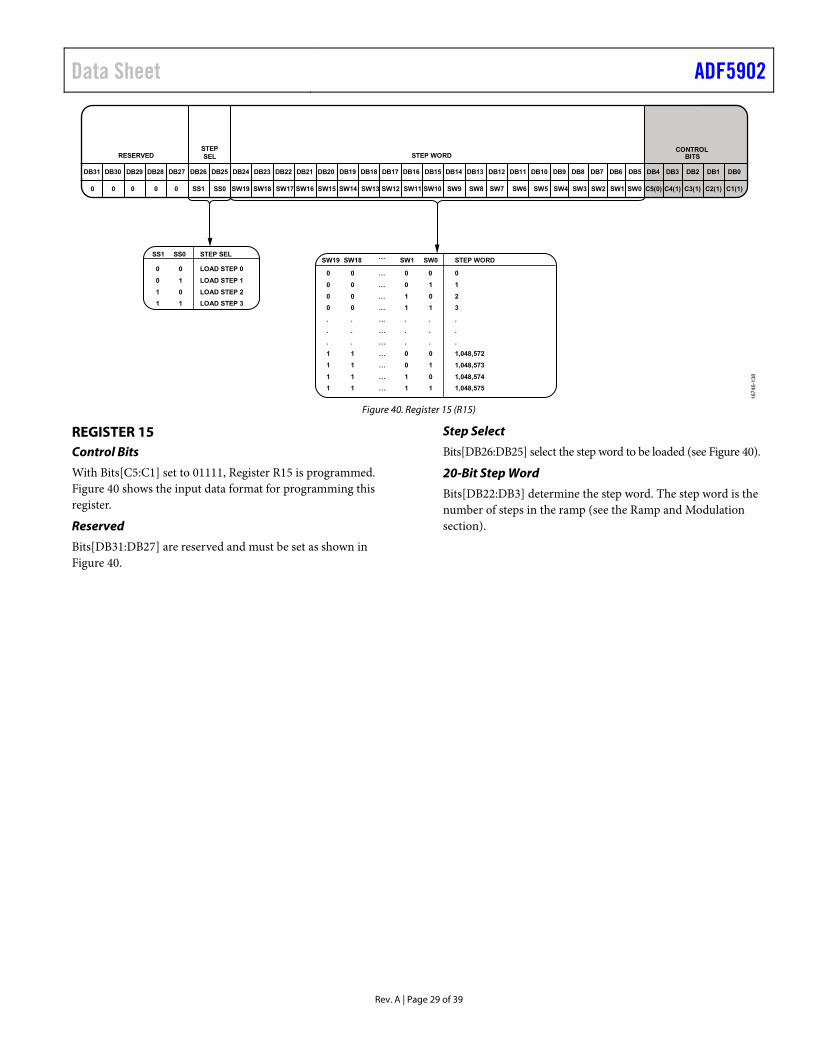
DB31 DB30 DB29 DB28 DB27 DB26 DB25 DB24 DB23 DB22 DB21 DB20 DB19 DB18 DB17 DB16 DB15 DB14 DB13 DB12 DB11 DB10 DB9 DB8 DB7 DB6 DB5 DB4 DB3 DB2 DB1 DB0
0 SS1 SS0 SW19
CONTROLBITS
SW18 SW17 SW16 SW15 SW14 SW13 SW12 SW11 SW10 SW9 SW8 SW7 SW6 SW5 SW4 SW3 SW2 SW1 SW0 C4(1) C3(1) C2(1) C1(1)
STEP WORD
C5(0)
STEPSEL
0 0 0 0
RESERVED
... STEP WORD
0 0 ... 0 0 0
0 0 ... 0 1 1
0 0 ... 1 0 2
0 0 ... 1 1 3
. . ... . . .
. . ... . . .
. . ... . . .
1 1 ... 0 0 1,048,572
1 1 ... 0 1 1,048,573
1 1 ... 1 0 1,048,574
1 1 ... 1 1 1,048,575
SW19 SW18 SW1 SW00 0
0 1
1 0
1 1
LOAD STEP 0
LOAD STEP 1
LOAD STEP 2
LOAD STEP 3
STEP SELSS1 SS0
167
46-
138
Figure 40. Register 15 (R15)
REGISTER 15 Control Bits
With Bits[C5:C1] set to 01111, Register R15 is programmed. Figure 40 shows the input data format for programming this register.
Reserved
Bits[DB31:DB27] are reserved and must be set as shown in Figure 40.
Step Select
Bits[DB26:DB25] select the step word to be loaded (see Figure 40).
20-Bit Step Word
Bits[DB22:DB3] determine the step word. The step word is the number of steps in the ramp (see the Ramp and Modulation section).

ADF5902 Data Sheet
Rev. A | Page 30 of 39
DB31 DB30 DB29 DB28 DB27 DB26 DB25 DB24 DB23 DB22 DB21 DB20 DB19 DB18 DB17 DB16 DB15 DB14 DB13 DB12 DB11 DB10 DB9 DB8 DB7 DB6 DB5 DB4 DB3 DB2 DB1 DB0
0 0 0 0 0 0 1 DSL1 DSL0
CONTROLBITS
TR1 RD DS11 DS10 DS9 DS8 DS7 DS6 DS5 DS4 DS3 DS2 DS1 DS0 C4(0) C3(0) C2(0) C1(0)
DELAY START WORD
C5(1)
RA
MP
DE
L
Tx_
DA
TA
RESERVED DEL SEL
DS11 DS10 ... DS1 DS0 DELAY START WORD
0 0 ... 0 0 0
0 0 ... 0 1 1
0 0 ... 1 0 2
0 0 ... 1 1 3
. . ... . . .
. . ... . . .
. . ... . . .
1 1 ... 0 0 4092
1 1 ... 0 1 4093
1 1 ... 1 0 4094
1 1 ... 1 1 4095
R D RAMP DEL
TR1 TX DATA TRIGGER
0 DISABLED
1 ENABLED
0 DISABLED
1 ENABLED
RE
SE
RV
ED
0
0 0
0 1
1 0
1 1
LOAD DELAY 0
LOAD DELAY 1
LOAD DELAY 2
LOAD DELAY 3
DELAY SELECTDSL1 DSL0
RE
SE
RV
ED
0
TR
IGG
ER
0 0
16
746
-13
9
Figure 41. Register 16 (R16)
DB31 DB30 DB29 DB28 DB27 DB26 DB25 DB24 DB23 DB22 DB21 DB20 DB19 DB18 DB17 DB16 DB15 DB14 DB13 DB12 DB11 DB10 DB9 DB8 DB7 DB6 DB5 DB4 DB3 DB2 DB1 DB0
0 0 0 0 0 0 0 0 C4(0) C3(0) C2(0) C1(1)
CONTROLBITS
RESERVED
C5(1)0 0 0 0 0 0 0 0 0 000 00 0 0 0 0 0
16
74
6-1
40
Figure 42. Register 17 (R17)
REGISTER 16 Control Bits
With Bits[C5:C1] set to 10000, Register R16 is programmed. Figure 41 shows the input data format for programming this register.
Reserved
Bits[DB31:DB25], Bits[DB22:DB21], and Bits[DB18:DB17] are reserved and must be set as shown in Figure 41.
Delay Select
Bits[DB24:DB23] select the delay word to be loaded.
TX_DATA Trigger
When Bit DB20 is set to 1, a logic high on the TX_DATA pin activates the ramp in conjunction with Bit DB29 of Register 5. Synchronize the active edge of the pulse applied to the TX_ DATA pin to the rising edge of the REFIN reference input.
The pulse duration applied to the TX_DATA pin must be a minimum width of 4 × 1/fPFD, where fPFD is the phase frequency detector (PFD) frequency.
When Bit DB20 is set to 0, this function is disabled.
When activating continuous triangular or continuous sawtooth ramps, a pulse applied to the TX_DATA pin is required after Bit DB29 of Register 5 is toggled high. To stop the continuous triangular or sawtooth ramps, a TX_DATA pulse is required after Bit DB29 of Register 5 is toggled low.
When Bit DB20 is set to 0, this function is disabled.
Ramp Delay
When Bit DB19 is set to 1, the delay between ramps function is enabled. When Bit DB19 is set to 0, this function is disabled.
12-Bit Delay Word
Bits[DB16:DB5] determine the delay word. The delay word determines the duration of the ramp start delay.
REGISTER 17 The bits in Register 17 are reserved and must be programmed as described in Figure 42 using a hexadecimal word of 0x00000011.

Data Sheet ADF5902
Rev. A | Page 31 of 39
APPLICATIONS INFORMATION INITIALIZATION SEQUENCE After powering up the device, administer the programming sequence shown in Table 7.
This sequence locks the VCO to 24.025 GHz with a 100 MHz reference. The ramp-up rate is 200 MHz at 144 μs. The ramp-down rate is 200 MHz at 9 μs.
Table 7. Initialization Sequence Step Register Hexadecimal Code Description 1 R7 0x02000007 Master reset 2 R11 0x0000002B Reset the counters 3 R11 0x0000000B Enable counters 4 R13 0x0018000D Enable ramp divider 5 R10 0x1D32A64A Reserved 6 R9 0x2A20B929 VCO calibration setup 7 R8 0x40003E88 Set the VCO frequency calibration divider clock to 100 kHz 8 R0 0x800FE520 Power up the device and LO
Delay of 10 μs
9 R7 0x01800827 PFD = 50 MHz, CLK1 = 2048 10 R6 0x00000006 Set the LSB FRAC = 0 11 R5 0x01E38005 N = 241.175 12 R4 0x00000004 Set the ATEST pin to high impedance 13 R3 0x01897803 Sets the I/O level to 3.3 V, CAL_BUSY to MUXOUT 14 R2 0x00020642 Set ADC clock to 1 MHz 15 R1 0xFFF7FFE1 Set the transmitter amplitude level 16 R0 0x800FE720 Start the VCO frequency calibration
Delay of 1200 μs
17 R0 0x800FE560 Turn Tx1 on, Tx2 off, and LO on 18 R0 0x800FED60 Tx1 amplitude calibration
Delay of 500 μs
19 R0 0x800FE5A0 Turn Tx1 off, Tx2 on, and LO on 20 R0 0x800FF5A0 Tx2 amplitude calibration
Delay of 500 μs
21 R17 0x00000011 Reserved 22 R16 0x00000010 Ramp delay register 23 R15 0x0000120F Load step register with STEP_SEL = 0, step word is 144 24 R15 0x0200012F Load step register with STEP_SEL = 1, step word is 9 25 R15 0x0400120F Load step register with STEP_SEL = 2, step word is 144 26 R15 0x0600012F Load step register with STEP_SEL = 3, step word is 9 27 R14 0x012038EE Load deviation register with DEV_SEL = 0, DEV = 455, DEV offset = 9 28 R14 0x033C720E Load deviation register with DEV_SEL = 1, dev word= −1820, DEV
offset = 9 29 R14 0x052038EE Load deviation register with DEV_SEL = 2, dev word = 455, dev offset = 9 30 R14 0x73C720E Load deviation register with DEV_SEL = 3, dev word = −1820 dev
offset = 9 31 R13 0x0018050D Load the clock register with CLK DIV SEL = 0, CLK2_0 = 10 32 R13 0x0018052D Load the clock register with CLK DIV SEL = 1, CLK2_1 = 10 33 R13 0x0018054D Load the clock register with CLK DIV SEL = 2, CLK2_2 = 10 34 R13 0x0018056D Load the clock register with CLK DIV SEL = 3, CLK2_3 = 10 35 R12 0x004F000C Charge pump current = 2.24 mA 36 R9 0x2800B929 Normal Operation 37 R7 0x0100A027 PFD = 100 MHz, CLK1 = 10 38 R6 0x00000006 Set the LSB FRAC = 0 39 R5 0x00F04005 INT =120, MSB FRAC = 512; lock to 24.025 GHz 40 R4 0x00002004 Ramp down to MUXOUT 41 R3 0x0189F803 I/O voltage level to 3.3 V
Delay of 100 μs
42 R11 0x0000010B Select ramp mode

ADF5902 Data Sheet
Rev. A | Page 32 of 39
RECALIBRATION SEQUENCE The ADF5902 can be recalibrated after the initialization sequence is complete and the device is powered up. The recalibration sequence must be run for every 10°C temperature change. The
temperature can be monitored using the temperature sensor (see the Temperature Sensor section).
Table 8. Recalibration Sequence Step Number from Initialization Sequence Register Hexadecimal Code Description R0 0x800FE500 Turn Tx1 off, Tx2 off and LO off 6 R9 0x2A20B929 Reserved 9 R7 0x01800827 PFD = 50 MHz, CLK1 = 2048 10 R6 0x00000006 Set the LSB FRAC = 0 11 R5 0x01E38005 N = 241.175 12 R4 0x00000004 Set the ATEST pin to high impedance 13 R3 0x01897803 I/O level to 3.3 V, CAL_BUSY to MUXOUT 14 R2 0x00020642 Set ADC clock to 1 MHz 15 R1 0xFFF7FFE1 Set the transmitter amplitude level R0 0x800FE700 Start the VCO frequency calibration Delay of 1200 μs 17 R0 0x800FE560 Turn Tx1 on, Tx2 off, and LO on 18 R0 0x800FED60 Tx1 amplitude calibration Delay of 500 μs 19 R0 0x800FE5A0 Turn Tx1 off, Tx2 on, and LO on 20 R0 0x800FF5A0 Tx2 amplitude calibration Delay of 500 μs 36 R9 0x2800B929 Reserved 37 R7 0x0100A027 PFD set to 100 MHz, CLK_DIV1 = 10 38 R6 0x00000006 Set the LSB FRAC = 0 39 R5 0x00F04005 Set INT word to 120, set MSB FRAC = 512; lock to
24.025 GHz 40 R4 0x00002004 Ramp down to MUXOUT 41 R3 0x0189F803 I/O voltage level to 3.3 V Delay of 100 μs 42 R11 0x0000010B Select ramp mode

Data Sheet ADF5902
Rev. A | Page 33 of 39
TEMPERATURE SENSOR The ADF5902 has an on-chip temperature sensor that can be accessed on the ATEST pin or as a digital word on DOUT following an ADC conversion. The temperature sensor operates over the full operating temperature range of −40°C to +105°C. The accuracy can be improved by performing a one-point calibration at room temperature and storing the result in memory.
With the temperature sensor on the analog test bus and test bus connected to the ATEST pin (Register 4 set to 0x0000A064), the ATEST voltage can be converted to temperature with the following equation:
GAIN
OFFATEST
VVV
eTemperatur
C)( (3)
where: VATEST is the voltage on the ATEST pin. VOFF = 0.699 V, the offset voltage. VGAIN = 6.4 × 10⁻³, the voltage gain.
The temperature sensor result can be converted to a digital word with the ADC and readback on DOUT with the following sequence:
1. Write 0x00012064 to Register R4 to connect the analog test bus to the ADC and the temperature sensor to the analog test bus.
2. Write 0x0002A802 to Register R2 to start the ADC conversion.
3. Write 0x0189FAC3 to Register R3 to set the ADC output data to DOUT.
4. Read back DOUT. 5. Write 0x00002064 to Register R4 to reset Register R4 to the
initial value. 6. Write 0x00020642 to Register R2 to reset Register R2 to the
initial value.
Convert the DOUT word to temperature with the following equation:
GAIN
OFFLSB
VVVADC
eTemperatur
C)( (4)
where: ADC is the ADC code read back on DOUT. VLSB = 7.33 mV, the ADC LSB voltage. VOFF = 0.699 V, the offset voltage. VGAIN = 6.4 × 10⁻³, the voltage gain.
RF SYNTHESIS: A WORKED EXAMPLE The following equation governs how to program the ADF5902:
RFOUT = (INT + (FRAC/225)) × fREF × 2 (5)
where: RFOUT is the RF frequency output. INT is the integer division factor. FRAC is the fractionality.
fREF = REFIN × ((1 + D)/(R × (1 + T))) (6)
where: REFIN is the reference frequency input. D is the reference doubler bit, DB10 in Register R7 (0 or 1). R is the reference division factor. T is the reference divide by 2 bit, DB11 in Register R7 (0 or 1).
For example, in a system where a 24.125 GHz RF frequency output (RFOUT) is required and a 100 MHz reference frequency input (REFIN) is available, fREF is set to 50 MHz.
From Equation 6,
fREF = (100 MHz × (1 + 0)/(1 × (1 + 1)) = 50 MHz
From Equation 5,
24.125 GHz = 50 MHz × (N + FRAC/225) × 2
Calculating the N and FRAC values,
N = int(RFOUT/(fREF × 2)) = 241 FRAC = FMSB × 213 + FLSB
FMSB = int(((RFOUT/(fREF × 2)) − N) × 212) = 1024 FLSB = int(((((RFOUT/(fREF × 2)) − N) × 212) − FMSB) × 213) = 0
where: FMSB is the 12-bit MSB FRAC value in Register R5. FLSB is the 13-bit LSB FRAC value in Register R6. int() makes an integer of the argument in parentheses.
REFERENCE DOUBLER The on-chip reference doubler allows the input reference signal to be doubled. This doubling is useful for increasing the PFD compar-ison frequency. Doubling the PFD frequency typically improves the noise performance of the system by 3 dB.

ADF5902 Data Sheet
Rev. A | Page 34 of 39
FREQUENCY MEASUREMENT PROCEDURE Use the following procedure to measure the output locked frequency of the ADF5902:
1. In Register R3, set the readback control bits (Bits[DB10:DB5]) to 26.
2. Read back the frequency counter value on DOUT and record this value as Frequency 1 (see Figure 3).
3. In Register R7, set the CLK1 bits (Bits[DB23:DB12]) to 1808.
4. In Register R13, set the CLK2 bits (Bits[DB18:DB7]) to 10. 5. In Register R5, set the ramp on bit (Bit DB29) to 0. 6. In Register R13, Set the clock divider mode bits
(Bits[DB20:DB19]) to 2. 7. Allow a minimum delay of 428 μs (CLKDIV/fPFD (sec)). 8. In Register R3, set the readback control bits
(Bits[DB10:DB5]) to 26. 9. Read back the frequency counter value on DOUT and
record this value as Frequency 2. Where Frequency 1 > Frequency 2,
Frequency Counter Value Delta = (216 − Frequency 1) + Frequency 2.
Where Frequency 2 > Frequency 1,
Frequency Counter Value Delta = Frequency 2 − Frequency 1.
10. Calculate the output frequency using the following formula:
Output Frequency = (Frequency Counter Value Delta/ CLKDIV) × fPFD × NDIV × 2
where: CLKDIV = ((CLK2 × 212) + CLK1). fPFD = fREF/RDIV. NDIV = INT value + (FRAC value/(225)).
11. Set Register R13 and Register R7 back to the original settings and enable the ramp function in Register R5 if required.
WAVEFORM GENERATION The ADF5902 is capable of generating five types of waveforms in the frequency domain: single ramp burst, single triangular burst, single sawtooth burst, continuous sawtooth ramp, and continuous triangular ramp. Figure 43 through Figure 47 show the types of waveforms available.
FR
EQ
UE
NC
Y
TIME 167
46-1
41
Figure 43. Single Ramp Burst
FR
EQ
UE
NC
TIME 167
46-
14
2
Figure 44. Single Triangular Burst
TIME
FR
EQ
UE
NC
Y
1674
6-1
43
Figure 45. Single Sawtooth Burst
FR
EQ
UE
NC
Y
TIME 167
16-1
44
Figure 46. Continuous Sawtooth Ramp
FR
EQ
UE
NC
Y
TIME 1674
6-14
5
Figure 47. Continuous Triangular Ramp
WAVEFORM DEVIATIONS AND TIMING TIMER
fDEV
FR
EQ
UE
NC
Y
TIME 16
74
6-1
46
Figure 48. Waveform Timing
The key parameters that define a ramp are
Frequency deviation Time per step Number of steps

Data Sheet ADF5902
Rev. A | Page 35 of 39
Frequency Deviation
The frequency deviation for each frequency hop is set by
fDEV = (fPFD/225) × (DEV × 2DEV_OFFSET) (7)
where: fPFD is the PFD frequency. DEV is a 16-bit word (Bits[DB20:DB5] in Register R14). DEV_OFFSET is a 4-bit word (Bits[DB24:DB21] in Register R14).
Time per step
The time between each frequency hop is set by
Timer = CLK1 × CLK2 × (1/fPFD) (8)
where: CLK1 and CLK2 are the 12-bit clock values (12-bit CLK1 divider in Register R7 and 12-bit CLK2 divider in Register R13).
Bits[DB20:DB19] in Register R13 must be set to 11 for ramp divider. fPFD is the PFD frequency.
Either CLK1 or CLK2 must be greater than 1, that is, CLK1 = CLK2 = 1 is not allowed.
Number of Steps
A 20-bit step value (Bits[DB24:DB5] in Register R15) defines the number of frequency hops that take place. The INT value cannot be incremented by more than 28 = 256 from its starting value.
RAMP AND MODULATION All ramps are generated according to the scheme shown in Figure 49. The total ramp is separated into four sections. Each section consists of a delay section and a slope section. Each slope is made up of one or more steps. Each step has a programmed frequency deviation and step time.
There are numerous ramp shapes available (see the Waveform Generation section). Depending on the chosen shape, some or all of the ramp slopes must be programmed. Figure 49 shows what must be programmed for each shape. The slope being programmed is controlled by
CLK DIV SEL (Register R13, Bits[DB6:DB5]). DEV SEL (Register R14, Bits[DB26:DB25]). Step SEL (Register R15, Bits[DB26:DB25]).
Typically, each register must be written multiple times, one time for each slope.
The frequency deviation for each step of a slope is set by
fDEV = (fPFD/225) × (DEV × 2DEV_OFFSET)
where: fDEV is the frequency deviation of a step. fPFD is the PFD frequency. DEV is the deviation value (Register R14, Bits[DB20:DB5]). DEV_OFFSET is the deviation offset (Register R14, Bits[DB24:DB21]).
The time for each step of a slope is set by
Timer = CLK1 × CLK2 × (1/fPFD)
where: Timer is the time per step. CLK1 is the CLK1 value (Register R7, Bits[23:12]). CLK2 is the CLK2 value (Register R13, Bits[18:7]).
CLK1 is common to all slopes.
The number of steps per slope is programmed in Register R15, Bits[DB24:DB5].
When programming the registers for a ramp, write the registers in descending order. Then write to Register R5 to enable the ramp (Register R5, Bit DB29 = 1) must be last.
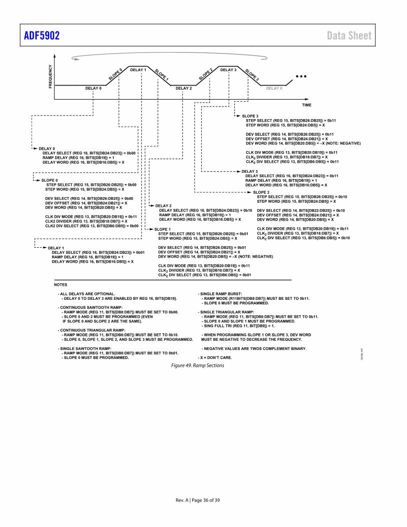
ADF5902 Data Sheet
Rev. A | Page 36 of 39
FR
EQ
UE
NC
Y
TIME
DELAY 0
DELAY 1
SLOPE 0
SLOPE 2SLOPE 1
SLOPE 3
DELAY 3
NOTES
- ALL DELAYS ARE OPTIONAL.- DELAY 0 TO DELAY 3 ARE ENABLED BY REG 16, BITS[DB19].
- CONTINUOUS SAWTOOTH RAMP:- RAMP MODE (REG 11, BITS[DB8:DB7]) MUST BE SET TO 0b00.- SLOPE 0 AND 2 MUST BE PROGRAMMED (EVEN IF SLOPE 0 AND SLOPE 2 ARE THE SAME).
- CONTINUOUS TRIANGULAR RAMP:- RAMP MODE (REG 11, BITS[DB8:DB7]) MUST BE SET TO 0b10.- SLOPE 0, SLOPE 1, SLOPE 2, AND SLOPE 3 MUST BE PROGRAMMED.
- SINGLE SAWTOOTH RAMP:- RAMP MODE (REG 11, BITS[DB8:DB7]) MUST BE SET TO 0b01.- SLOPE 0 MUST BE PROGRAMMED.
- SINGLE RAMP BURST:- RAMP MODE (R11BITS[DB8:DB7]) MUST BE SET TO 0b11.- SLOPE 0 MUST BE PROGRAMMED.
- SINGLE TRIANGULAR RAMP:- RAMP MODE (REG 11, BITS[DB8:DB7]) MUST BE SET TO 0b11.- SLOPE 0 AND SLOPE 1 MUST BE PROGRAMMED.- SING FULL TRI (REG 11, BIT[DB9]) = 1.
- WHEN PROGRAMMING SLOPE 1 OR SLOPE 3, DEV WORD MUST BE NEGATIVE TO DECREASE THE FREQUENCY.
- NEGATIVE VALUES ARE TWOS COMPLEMENT BINARY.
- X = DON’T CARE.
SLOPE 3STEP SELECT (REG 15, BITS[DB26:DB25]) = 0b11STEP WORD (REG 15, BITS[DB24:DB5]) = X
DEV SELECT (REG 14, BITS[DB26:DB25]) = 0b11DEV OFFSET (REG 14, BITS[DB24:DB21]) = XDEV WORD (REG 14, BITS[DB20:DB5]) = –X (NOTE: NEGATIVE)
CLK DIV MODE (REG 13, BITS[DB20:DB19]) = 0b11CLK2 DIVIDER (REG 13, BITS[DB18:DB7]) = XCLK2 DIV SELECT (REG 13, BITS[DB6:DB5]) = 0b11
DELAY 3DELAY SELECT (REG 16, BITS[DB24:DB23]) = 0b11RAMP DELAY (REG 16, BITS[DB19]) = 1DELAY WORD (REG 16, BITS[DB16:DB5]) = X
SLOPE 2STEP SELECT (REG 15, BITS[DB26:DB25]) = 0b10STEP WORD (REG 15, BITS[DB24:DB5]) = X
DEV SELECT (REG 14, BITS[DB22:DB25]) = 0b10DEV OFFSET (REG 14, BITS[DB24:DB21]) = XDEV WORD (REG 14, BITS[DB20:DB5]) = X
CLK DIV MODE (REG 13, BITS[DB20:DB19]) = 0b11CLK2 DIVIDER (REG 13, BITS[DB18:DB7]) = XCLK2 DIV SELECT (REG 13, BITS[DB6:DB5]) = 0b10
SLOPE 1STEP SELECT (REG 15, BITS[DB26:DB25]) = 0b01STEP WORD (REG 15, BITS[DB24:DB5]) = X
DEV SELECT (REG 14, BITS[DB26:DB25]) = 0b01DEV OFFSET (REG 14, BITS[DB24:DB21]) = XDEV WORD (REG 14, BITS[DB20:DB5]) = –X (NOTE: NEGATIVE)
CLK DIV MODE (REG 13, BITS[DB20:DB19]) = 0b11CLK2 DIVIDER (REG 13, BITS[DB18:DB7]) = XCLK2 DIV SELECT (REG 13, BITS[DB6:DB5]) = 0b01
SLOPE 0 STEP SELECT (REG 15, BITS[DB26:DB25]) = 0b00STEP WORD (REG 15, BITS[DB24:DB5]) = X
DEV SELECT (REG 14, BITS[DB26:DB25]) = 0b00DEV OFFSET (REG 14, BITS[DB24:DB21]) = XDEV WORD (REG 14, BITS[DB20:DB5]) = X
CLK DIV MODE (REG 13, BITS[DB20:DB19]) = 0b11CLK2 DIVIDER (REG 13, BITS[DB18:DB7]) = XCLK2 DIV SELECT (REG 13, BITS[DB6:DB5]) = 0b00
DELAY 2DELAY SELECT (REG 16, BITS[DB24:DB23]) = 0b10RAMP DELAY (REG 16, BITS[DB19]) = 1DELAY WORD (REG 16, BITS[DB16:DB5]) = X
DELAY 1DELAY SELECT (REG 16, BITS[DB24:DB23]) = 0b01RAMP DELAY (REG 16, BITS[DB19]) = 1DELAY WORD (REG 16, BITS[DB16:DB5]) = X
DELAY 0DELAY SELECT (REG 16, BITS[DB24:DB23]) = 0b00RAMP DELAY (REG 16, BITS[DB19]) = 1DELAY WORD (REG 16, BITS[DB16:DB5]) = X
DELAY 0DELAY 2
167
46-1
47
Figure 49. Ramp Sections

Data Sheet ADF5902
Rev. A | Page 37 of 39
Ramp Complete and Ramp-Down Signals to MUXOUT
Figure 50 shows the ramp complete signal on MUXOUT.
FR
EQ
UE
NC
Y
TIME
VO
LT
AG
E
TIME 1674
6-1
48
Figure 50. Ramp Complete Signal on MUXOUT
To activate this function, set Bits[DB15:DB12] in Register R3 to 1111, and set Bits[DB19:DB5] in Register R4 to 0x00C0.
Figure 51 shows the ramp-down signal on MUXOUT.
FR
EQ
UE
NC
Y
TIME
VO
LT
AG
E
TIME 1674
6-1
49
Figure 51. Ramp-Down Signal on MUXOUT
To activate this function, set Bits[DB15:DB12] in Register R3 to 1111, and set Bits[DB19:DB5] in Register R4 to 0x0100.
External Control of Ramp Steps
The internal ramp clock can be bypassed and each step can be triggered by a pulse on the TX_DATA pin. This process allows transparent control of each step. Enable this feature by setting Bit DB30 in Register R14 to 1.
FR
EQ
UE
NC
Y
TIME
TX_DATA
RFOUT
VO
LT
AG
E
TIME 167
46-1
50
Figure 52. External Control of Ramp Steps
APPLICATION OF THE ADF5902 IN FMCW RADAR Figure 53 shows the application of the ADF5902 in a frequency modulated continuous wave (FMCW) radar system.
In the FMCW radar system, the ADF5902 generates the sawtooth or triangle ramps necessary for this type of radar to operate.
The ADF5902 CPOUT pin controls the VTUNE pin on the ADF5902 transmitter MMIC and thus the frequency of the VCO and the transmitter output signal on TXOUT1 or TXOUT2. The LO signal from the ADF5902 is fed to the LO input on the ADF5904.
The ADF5904 downconverts the signal from the four receiver antennas to baseband with the LO signal from the transmitter MMIC.
The downconverted baseband signals from the four receiver channels on the ADF5904 are fed to the ADAR7251 4-channel, continuous time, Σ-Δ ADC.
A digital signal processor (DSP) follows the ADC to handle the target information processing.

ADF5902 Data Sheet
Rev. A | Page 38 of 39
ADF5902
ADF5904
TXOUT1
TXOUT2
RX3_RF
RX2_RF
RX1_RF
RX4_RF
LO_IN
LOOUT
ADAR7251DSP Rx BASEBAND
LOOP FILTER
VTUNECPOUT
167
46-
031
Figure 53. FMCW Radar with the ADF5902

Data Sheet ADF5902
Rev. A | Page 39 of 39
OUTLINE DIMENSIONS
0.500.400.30
10-2
0-2
017
-C
1
0.50BSC
BOTTOM VIEWTOP VIEW
TOP VIEW
PIN 1INDICATOR
32
916
17
24
25
8
EXPOSEDPAD
SEATINGPLANE
0.05 MAX0.02 NOM
0.20 REF
COPLANARITY0.08
0.300.250.18
5.105.00 SQ4.90
0.800.750.70
FOR PROPER CONNECTION OFTHE EXPOSED PAD, REFER TOTHE PIN CONFIGURATION ANDFUNCTION DESCRIPTIONSSECTION OF THIS DATA SHEET.
0.20 MIN
3.753.60 SQ3.55
COMPLIANT TO JEDEC STANDARDS MO-220-WHHD-5PK
G-0
0457
0
PIN 1INDIC ATOR AREA OPTIONS(SEE DETAIL A)
DETAIL A(JEDEC 95)
Figure 54. 32-Lead Lead Frame Chip Scale Package [LFCSP]
5 mm × 5 mm Body and 0.75 mm Package Height (CP-32-12)
ORDERING GUIDE Model1 Temperature Range Package Description Package Option ADF5902WCCPZ −40°C to +105°C 32-Lead Lead Frame Chip Scale Package [LFCSP] CP-32-12 ADF5902WCCPZ-RL7 −40°C to +105°C 32-Lead Lead Frame Chip Scale Package [LFCSP] CP-32-12 EV-ADF5902SD1Z Evaluation Board 1 Z = RoHS Compliant Part.
AUTOMOTIVE PRODUCTS The ADF5902W models are available with controlled manufacturing to support the quality and reliability requirements of automotive applications. Note that these automotive models may have specifications that differ from the commercial models; therefore, designers should review the Specifications section of this data sheet carefully. Only the automotive grade products shown are available for use in automotive applications. Contact your local Analog Devices account representative for specific product ordering information and to obtain the specific Automotive Reliability reports for these models.
©2018–2020 Analog Devices, Inc. All rights reserved. Trademarks and registered trademarks are the property of their respective owners. D16746-0-1/20(A)

Mouser Electronics
Authorized Distributor
Click to View Pricing, Inventory, Delivery & Lifecycle Information: Analog Devices Inc.:
EV-ADF5902SD1Z ADF5902WCCPZ ADF5902WCCPZ-RL7