24bit 4ch codec with mic/hp/spk/line-amp - akm.com · ak4695ecb -30 ~ +85°c 42pin csp (0.5mm...
TRANSCRIPT

[AK4695]
MS1463-E-01 2014/12
- 1 -
GENERAL DESCRIPTION
The AK4695 is a low power consumption 24bit stereo CODEC with microphone, headphone, speaker and line amplifiers. The input circuits include 4ch microphone amplifiers, input selectors and an ALC (Automatic Level Control) circuit, and the output circuits include a line amplifier, a cap-less headphone amplifier and a speaker amplifier. It is suitable for portable application with recording/playback function. The integrated charge pump circuit generates a negative voltage and removes the output AC coupling capacitors. The AK4695 is available in a small 42pin CSP, utilizing less board space than competitive offerings.
FEATURES
1. Recording Function
Two Low Noise MIC Power Supplies
Stereo Single-ended input with five Selectors
Low Noise MIC Amplifier: +30dB ~ +24dB (3dB Step), +21dB ~ +3dB (1.5dB Step)
ADC Performance: S/(N+D): 86dB, DR, S/N: 98dB (MIC-Amp=+21dB)
S/(N+D): 93dB, DR, S/N: 103dB (MIC-Amp=+12dB)
Microphone Sensitivity Compensation: 0dB ~ 9dB, 0.75dB Step
HPF x 2/LPF, 2-band Equalizer
4ch Digital ALC (Automatic Level Control)
(Setting Range: +54dB ~ 36dB, 0.375dB Step)
Soft Mute
4ch Digital MIC Interface
2. Playback Function
Digital ALC (Automatic Level Control)
(Setting Range: +54dB ~ 36dB, 0.375dB Step)
3-band Dynamic Range Control Circuit
Digital Volume Control (+12dB ~ 115dB, 0.5dB Step, Mute)
Stereo Line Amplifier
- Output Power: [email protected]%, 22k (AVDD=2.8V)
Capacitor-less Stereo Headphone Amplifier
- HP-AMP Performance: S/(N+D): 75dB@15mW
- Output Power: 30mW@16
- Pop Noise Free at Power-ON/OFF
Mono Speaker Amplifier (with Stereo Line Output Switch)
- SPK-AMP Performance: S/(N+D): 70dB@250mW
- BTL Output
- Output Power: 400mW@10%, 6 (SVDD=2.8V)
- Thermal Shutdown
- Beep Input: +16dB ~ +2dB, 2dB Step
3. Power Management
4. Master Clock: 256fs, 512fs or 1024fs (MCKI pin)
5. Sampling Frequency: 8kHz ~ 48kHz (256fs, 512fs), 8kHz ~ 16kHz (1024fs)
24bit 4ch CODEC with MIC/HP/SPK/LINE-AMP
AK4695

[AK4695]
MS1463-E-01 2014/12
- 2 -
6. Audio Interface Format: MSB First, 2’s complement
ADC: 24bit MSB justified, 16/24bit I2S
DAC: 24bit MSB justified, 16/24bit LSB justified, 16/24bit I2S
7. Serial P I/F: 3-wire Serial
8. General Purpose Output
9. Ta = 30 85C
10. Power Supply:
Analog Power Supply (AVDD): 2.7 ~ 3.5V
Digital & Headphone Power Supply (DVDD): 1.6 ~ 2.0V
Digital I/O Power Supply (TVDD): 1.6 or (DVDD-0.2) ~ 3.5V
Speaker & Charge-pump Power Supply (SVDD): 2.7 ~ 3.5V
11. Package: 42pin CSP (2.96 x 3.46mm, 0.5mm pitch)
[AK4695]
MS1463-E-01 2014/12
- 3 -
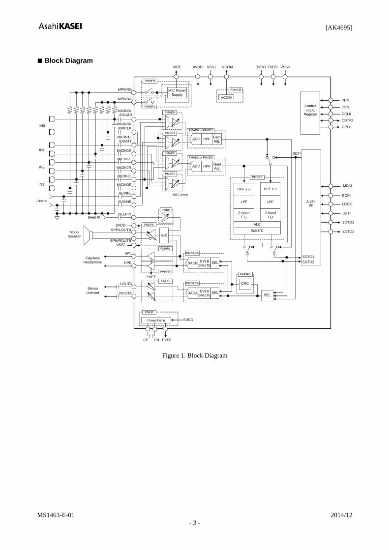
Block Diagram
MIC Power Supply
HPF
PMAD0 or PMAD1
Audio I/F
IN0
Cap-less Headphone
Mono Speaker
Control Logic,
Register
MPWRB
MICIN0L /DDAT0
MICIN0R /DMCLK
MICIN1L /DDAT1
MICIN1R
SPP/LOUTB
SPN/ROUTB
SVDD
AVDD VSS1 TVDD
CCLK
CDTIO
BCKI
LRCK
SDTO1
SDTI
MCKI
PMHPL
HPL
HPR
VSS3
CSN
2-band EQ
PMDSP
PDN
PMAD0
SDTI
SDTO1
PMDACA
PMSPK
ADC
MICIN2L
MICIN2R
PMAD1
Charge Pump
PVEE CP CN
MPWRA
MIC-Amp
VCOM DVDD
SVDD
PMHP
GPO1
SDTO2
LPF
HPF x 2
Line In
AUXINL
AUXINR
2-band EQ
LPF
HPF x 2
HPF
PMAD2 or PMAD3
PMAD2
ADC
PMAD3 MICIN3L
MICIN3R
IN1
IN2
IN3
SDTO2
SEL
BEEPIN Beep In
Stereo Line-out
PMLO LOUTA
ROUTA
PVEE
MRF
VCOM
PMVCM
ALC
MIX
PMDRC
SMUTE
PMDACB
DACA
DACB DVLB
SMUTE
DVLA SMUTE
PMBP
PMMPA
PMMPB
SEL
SEL
DRC
Gain Adj.
Gain Adj.
VSS2
PMHPR
Figure 1. Block Diagram

[AK4695]
MS1463-E-01 2014/12
- 4 -
Ordering Guide
AK4695ECB -30 ~ +85°C 42pin CSP (0.5mm pitch), Black Type
AKD4695 Evaluation board for AK4695
Pin Layout
6
5
4
3
2
1
F E D C B A
Top View
G
6 MICIN2R MICIN2L MPWRB MPWRA VCOM LOUTA ROUTA
5 MICIN3R MICIN3L MRF AVDD VSS1 VSS2 SPP/
LOUTB
4 MICIN1L MICIN1R MICIN0R MICIN0L BEEPIN SPN/
ROUTB SVDD
3 AUXINL PDN TVDD LRCK BCKI CP CN
2 AUXINR VSS3 CSN SDTI SDTO1 DVDD PVEE
1 GPO1 MCKI CCLK CDTIO SDTO2 HPL HPR
A B C D E F G
Top View
[AK4695]
MS1463-E-01 2014/12
- 5 -
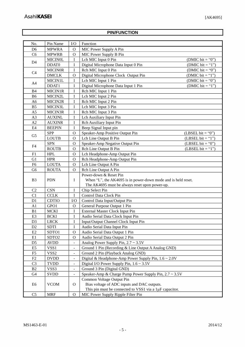
PIN/FUNCTION
No. Pin Name I/O Function
D6 MPWRA O MIC Power Supply A Pin
C6 MPWRB O MIC Power Supply B Pin
D4 MICIN0L I Lch MIC Input 0 Pin (DMIC bit = “0”)
DDAT0 I Digital Microphone Data Input 0 Pin (DMIC bit = “1”)
C4 MICIN0R I Rch MIC Input 0 Pin (DMIC bit = “0”)
DMCLK O Digital Microphone Clock Output Pin (DMIC bit = “1”)
A4 MICIN1L I Lch MIC Input 1 Pin (DMIC bit = “0”)
DDAT1 I Digital Microphone Data Input 1 Pin (DMIC bit = “1”)
B4 MICIN1R I Rch MIC Input 1 Pin
B6 MICIN2L I Lch MIC Input 2 Pin
A6 MICIN2R I Rch MIC Input 2 Pin
B5 MICIN3L I Lch MIC Input 3 Pin
A5 MICIN3R I Rch MIC Input 3 Pin
A3 AUXINL I Lch Auxiliary Input Pin
A2 AUXINR I Rch Auxiliary Input Pin
E4 BEEPIN I Beep Signal Input pin
G5 SPP O Speaker-Amp Positive Output Pin (LBSEL bit = “0”)
LOUTB O Lch Line Output B Pin (LBSEL bit = “1”)
F4 SPN O Speaker-Amp Negative Output Pin (LBSEL bit = “0”)
ROUTB O Rch Line Output B Pin (LBSEL bit = “1”)
F1 HPL O Lch Headphone-Amp Output Pin
G1 HPR O Rch Headphone-Amp Output Pin
F6 LOUTA O Lch Line Output A Pin
G6 ROUTA O Rch Line Output A Pin
B3 PDN I
Power-down & Reset Pin
When “L”, the AK4695 is in power-down mode and is held reset.
The AK4695 must be always reset upon power-up.
C2 CSN I Chip Select Pin
C1 CCLK I Control Data Clock Pin
D1 CDTIO I/O Control Data Input/Output Pin
A1 GPO1 O General Purpose Output 1 Pin
B1 MCKI I External Master Clock Input Pin
E3 BCKI I Audio Serial Data Clock Input Pin
D3 LRCK I Input/Output Channel Clock Input Pin
D2 SDTI I Audio Serial Data Input Pin
E2 SDTO1 O Audio Serial Data Output 1 Pin
E1 SDTO2 O Audio Serial Data Output 2 Pin
D5 AVDD - Analog Power Supply Pin, 2.7 ~ 3.5V
E5 VSS1 - Ground 1 Pin (Recording & Line Output A Analog GND)
F5 VSS2 - Ground 2 Pin (Playback Analog GND)
F2 DVDD - Digital & Headphone-Amp Power Supply Pin, 1.6 ~ 2.0V
C3 TVDD - Digital I/O Power Supply Pin, 1.6 ~ 3.5V
B2 VSS3 - Ground 3 Pin (Digital GND)
G4 SVDD - Speaker-Amp & Charge Pump Power Supply Pin, 2.7 ~ 3.5V
E6 VCOM O
Common Voltage Output Pin
Bias voltage of ADC inputs and DAC outputs.
This pin must be connected to VSS1 via a 1μF capacitor.
C5 MRF O MIC Power Supply Ripple Filter Pin
[AK4695]
MS1463-E-01 2014/12
- 6 -
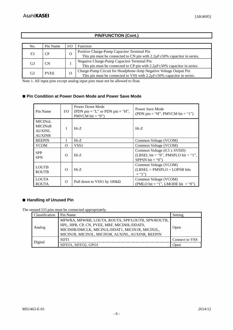
PIN/FUNCTION (Cont.)
No. Pin Name I/O Function
F3 CP O Positive Charge-Pump Capacitor Terminal Pin
This pin must be connected to CN pin with 2.2μF±50% capacitor in series.
G3 CN I Negative Charge-Pump Capacitor Terminal Pin
This pin must be connected to CP pin with 2.2μF±50% capacitor in series.
G2 PVEE O Charge-Pump Circuit for Headphone-Amp Negative Voltage Output Pin
This pin must be connected to VSS with 2.2μF±50% capacitor in series.
Note 1. All input pins except analog input pins must not be allowed to float.
Pin Condition at Power Down Mode and Power Save Mode
Pin Name I/O
Power Down Mode
(PDN pin = “L” or PDN pin = “H”,
PMVCM bit = “0”)
Power Save Mode
(PDN pin = “H”, PMVCM bit = “1”)
MICINxL
MICINxR
AUXINL
AUXINR
I Hi-Z Hi-Z
BEEPIN I Hi-Z Common Voltage (VCOM)
VCOM O VSS1 Common Voltage (VCOM)
SPP
SPN O Hi-Z
Common Voltage (0.5 x SVDD)
(LBSEL bit = “0”, PMSPLO bit = “1”,
SPPSN bit = “0”)
LOUTB
ROUTB O Hi-Z
Common Voltage (VCOM)
(LBSEL = PMSPLO = LOPSB bits
= “1”)
LOUTA
ROUTA O Pull down to VSS1 by 100kΩ
Common Voltage (VCOM)
(PMLO bit = “1”, LMODE bit = “0”)
Handling of Unused Pin
The unused I/O pins must be connected appropriately.
Classification Pin Name Setting
Analog
MPWRA, MPWRB, LOUTA, ROUTA, SPP/LOUTB, SPN/ROUTB,
HPL, HPR, CP, CN, PVEE, MRF, MICIN0L/DDAT0,
MICIN0R/DMCLK, MICIN1L/DDAT1, MICIN1R, MICIN2L,
MICIN2R, MICIN3L, MICIN3R, AUXINL, AUXINR, BEEPIN
Open
Digital SDTI Connect to VSS
SDTO1, SDTO2, GPO1 Open

[AK4695]
MS1463-E-01 2014/12
- 7 -
ABSOLUTE MAXIMUM RATINGS
(VSS1=VSS2=VSS3=0V; Note 2)
Parameter Symbol min max Unit
Power Supplies: Analog AVDD 0.3 6.0 V
Digital & Headphone-Amp DVDD 0.3 2.5 V
Digital I/O TVDD 0.3 6.0 V
Speaker-Amp & Charge Pump SVDD 0.3 6.0 V
Input Current, Any Pin Except Supplies IIN - 10 mA
Analog Input Voltage (Note 4) VINA 0.3 AVDD+0.3 V
Digital Input Voltage (Note 5) VIND 0.3 TVDD+0.3 V
Ambient Temperature (powered applied) Ta 30 85 C
Storage Temperature Tstg 65 150 C
Maximum Power Dissipation (Note 6) Pd - 920 mW
Note 2. All voltages are with respect to ground.
Note 3. VSS1, VSS2 and VSS3 must be connected to the same analog ground plane.
Note 4. MICIN0L, MICIN0R, MICIN1L, MICIN1R, MICIN2L, MICIN2R, MICIN3L, MICIN3R, AUXINL, AUXINR,
BEEPIN pins
Note 5. PDN, CSN, CCLK, CDTIO, SDTI, LRCK, BCKI, MCKI pins
Note 6. This power is the AK4695 internal dissipation that does not include power dissipation of externally connected
headphone and speaker. The maximum junction temperature is 125C and θja (Junction to Ambient) is 42.5C/W at
JESD51-9 (2p2s). When Pd =920mW and the θja is 42.5C/W, the junction temperature does not exceed 125C. In
this case, there is no case that the AK4695 is damaged by its internal power dissipation. Therefore, the AK4695
should be used in the condition of θja ≤ 42.5C/W.
WARNING: Operation at or beyond these limits may result in permanent damage to the device.
Normal operation is not guaranteed at these extremes.
[AK4695]
MS1463-E-01 2014/12
- 8 -
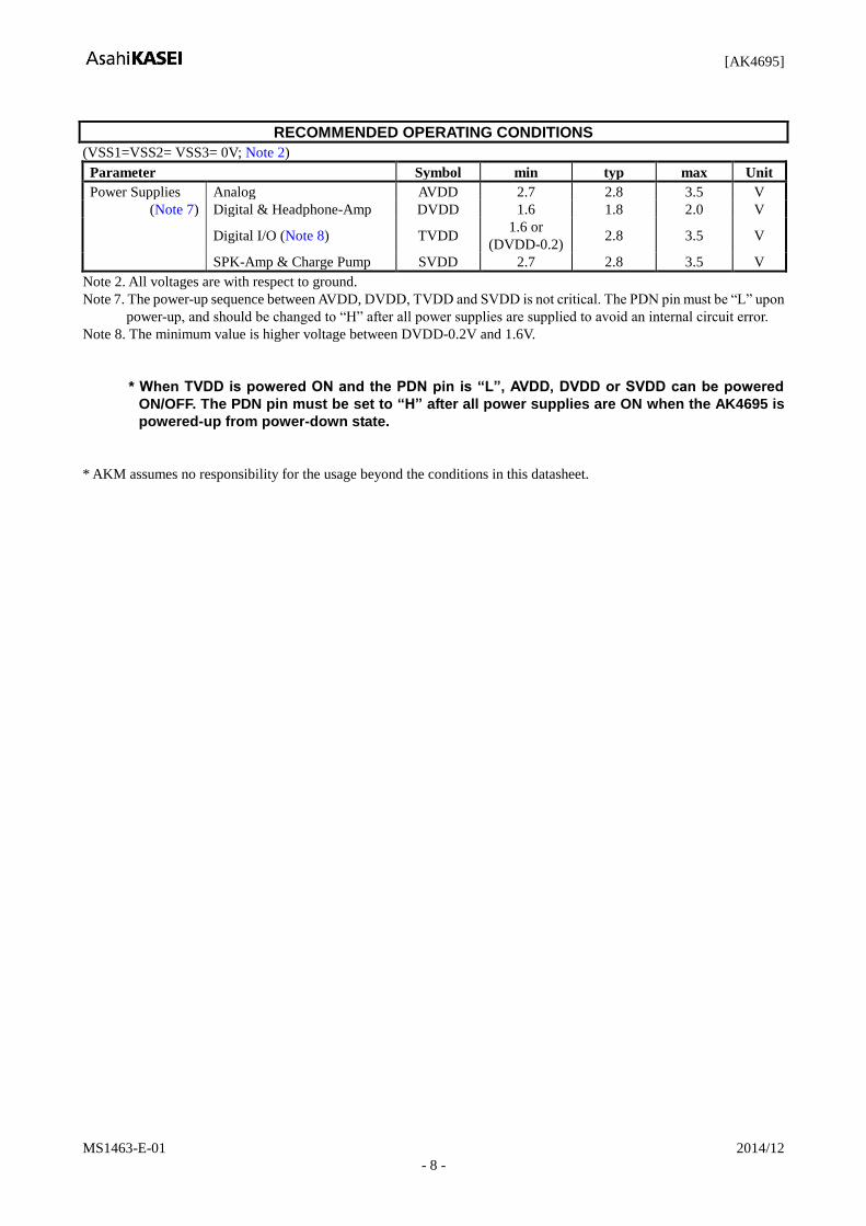
RECOMMENDED OPERATING CONDITIONS
(VSS1=VSS2= VSS3= 0V; Note 2)
Parameter Symbol min typ max Unit
Power Supplies Analog AVDD 2.7 2.8 3.5 V
(Note 7) Digital & Headphone-Amp DVDD 1.6 1.8 2.0 V
Digital I/O (Note 8) TVDD 1.6 or
(DVDD-0.2) 2.8 3.5 V
SPK-Amp & Charge Pump SVDD 2.7 2.8 3.5 V
18HNote 2. All voltages are with respect to ground.
Note 7. The power-up sequence between AVDD, DVDD, TVDD and SVDD is not critical. The PDN pin must be “L” upon
power-up, and should be changed to “H” after all power supplies are supplied to avoid an internal circuit error.
Note 8. The minimum value is higher voltage between DVDD-0.2V and 1.6V.
* When TVDD is powered ON and the PDN pin is “L”, AVDD, DVDD or SVDD can be powered
ON/OFF. The PDN pin must be set to “H” after all power supplies are ON when the AK4695 is
powered-up from power-down state.
* AKM assumes no responsibility for the usage beyond the conditions in this datasheet.
[AK4695]
MS1463-E-01 2014/12
- 9 -
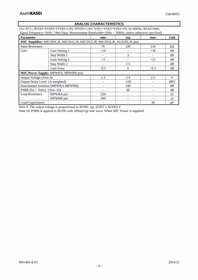
ANALOG CHARACTERISTICS
(Ta=25C; AVDD=SVDD=TVDD=2.8V, DVDD=1.8V; VSS1=VSS2=VSS3=0V; fs=48kHz, BCKI=64fs;
Signal Frequency=1kHz; 24bit Data; Measurement Bandwidth=20Hz 20kHz; unless otherwise specified)
Parameter min typ max Unit
MIC Amplifier: MICIN0L/R, MICIN1L/R, MICIN2L/R, MICIN3L/R, AUXINL/R pins
Input Resistance 70 100 130 k
Gain Gain Setting 1 +24 - +30 dB
Step Width 1 - 3 - dB
Gain Setting 2 +3 - +21 dB
Step Width 2 - 1.5 - dB
Gain Error -0.5 0 +0.5 dB
MIC Power Supply: MPWRA, MPWRB pins
Output Voltage (Note 9) 2.3 2.4 2.5 V
Output Noise Level (A-weighted) - -120 - dBV
Interchannel Isolation (MPWRA-MPWRB) - 100 - dB
PSRR (fin = 1kHz) (Note 10) - 60 - dB
Load Resistance MPWRA pin 250 - -
MPWRB pin 500 - -
Load Capacitance - - 30 pF
Note 9. The output voltage is proportional to AVDD. typ. (0.857 x AVDD) V
Note 10. PSRR is applied to AVDD with 100mpVpp sine wave. When MIC Power is supplied.
[AK4695]
MS1463-E-01 2014/12
- 10 -
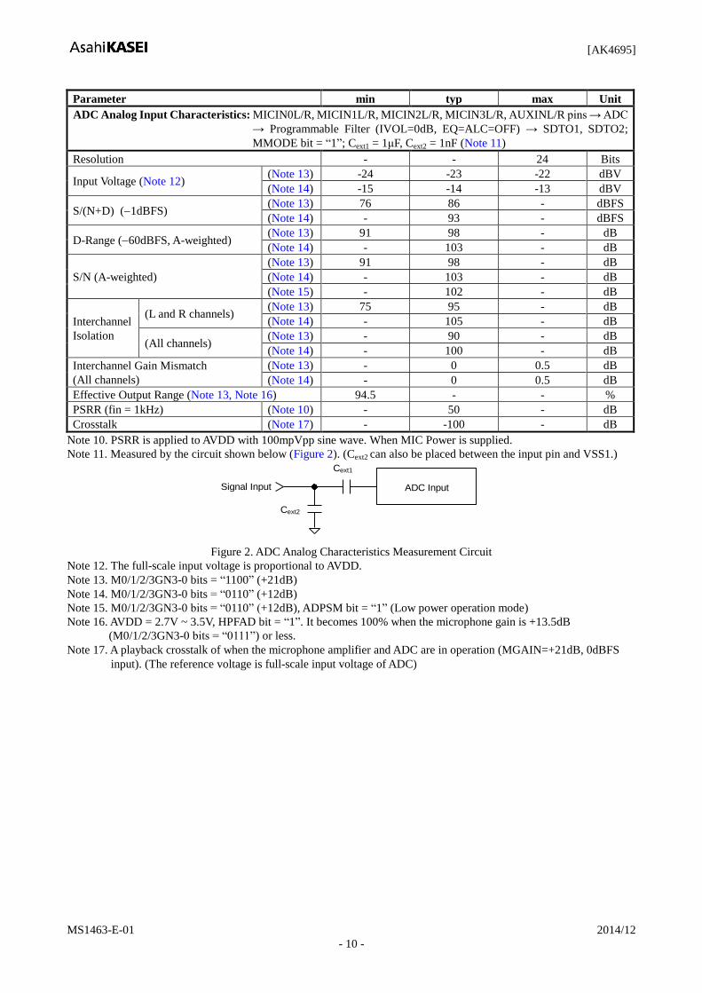
Parameter min typ max Unit
ADC Analog Input Characteristics: MICIN0L/R, MICIN1L/R, MICIN2L/R, MICIN3L/R, AUXINL/R pins → ADC
→ Programmable Filter (IVOL=0dB, EQ=ALC=OFF) → SDTO1, SDTO2;
MMODE bit = “1”; Cext1 = 1μF, Cext2 = 1nF (Note 11)
Resolution - - 24 Bits
Input Voltage (Note 12) (Note 13) -24 -23 -22 dBV
(Note 14) -15 -14 -13 dBV
S/(N+D) (1dBFS) (Note 13) 76 86 - dBFS
(Note 14) - 93 - dBFS
D-Range (60dBFS, A-weighted) (Note 13) 91 98 - dB
(Note 14) - 103 - dB
S/N (A-weighted)
(Note 13) 91 98 - dB
(Note 14) - 103 - dB
(Note 15) - 102 - dB
Interchannel
Isolation
(L and R channels) (Note 13) 75 95 - dB
(Note 14) - 105 - dB
(All channels) (Note 13) - 90 - dB
(Note 14) - 100 - dB
Interchannel Gain Mismatch
(All channels)
(Note 13) - 0 0.5 dB
(Note 14) - 0 0.5 dB
Effective Output Range (Note 13, Note 16) 94.5 - - %
PSRR (fin = 1kHz) (Note 10) - 50 - dB
Crosstalk (Note 17) - -100 - dB
Note 10. PSRR is applied to AVDD with 100mpVpp sine wave. When MIC Power is supplied.
Note 11. Measured by the circuit shown below (Figure 2). (Cext2 can also be placed between the input pin and VSS1.)
ADC Input
Cext2
Cext1
Signal Input
Figure 2. ADC Analog Characteristics Measurement Circuit
Note 12. The full-scale input voltage is proportional to AVDD.
Note 13. M0/1/2/3GN3-0 bits = “1100” (+21dB)
Note 14. M0/1/2/3GN3-0 bits = “0110” (+12dB)
Note 15. M0/1/2/3GN3-0 bits = “0110” (+12dB), ADPSM bit = “1” (Low power operation mode)
Note 16. AVDD = 2.7V ~ 3.5V, HPFAD bit = “1”. It becomes 100% when the microphone gain is +13.5dB
(M0/1/2/3GN3-0 bits = “0111”) or less.
Note 17. A playback crosstalk of when the microphone amplifier and ADC are in operation (MGAIN=+21dB, 0dBFS
input). (The reference voltage is full-scale input voltage of ADC)
[AK4695]
MS1463-E-01 2014/12
- 11 -
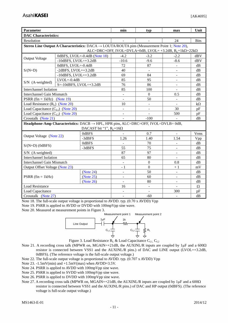
Parameter min typ max Unit
DAC Characteristics:
Resolution - - 24 Bits
Stereo Line Output A Characteristics: DACA → LOUTA/ROUTA pins (Measurement Point 1; Note 20),
ALC=DRC=OFF, IVOL=DVLA=0dB, LVOL= +3.2dB, RL=1k+22k
Output Voltage 0dBFS, LVOL=-0.4dB (Note 18) -4.2 -3.2 -2.2 dBV
-10dBFS, LVOL=+3.2dB -10.6 -9.6 -8.6 dBV
S/(N+D)
0dBFS, LVOL=-0.4dB 72 87 - dB
-2dBFS, LVOL=+3.2dB 40 - - dB
-10dBFS, LVOL=+3.2dB 69 84 - dB
S/N (A-weighted) LVOL=-0.4dB 85 95 - dB
S=-10dBFS, LVOL=+3.2dB 76 86 - dB
Interchannel Isolation 85 100 - dB
Interchannel Gain Mismatch - 0 0.5 dB
PSRR (fin = 1kHz) (Note 19) - 50 - dB
Load Resistance (RL) (Note 20) 10 - - k
Load Capacitance (CL1) (Note 20) - - 30 pF
Load Capacitance (CL2) (Note 20) - - 500 pF
Crosstalk (Note 21) - -100 - dB
Headphone-Amp Characteristics: DACB → HPL, HPR pins, ALC=DRC=OFF, IVOL=DVLB= 0dB,
DACAST bit “1”, RL=16
Output Voltage (Note 22) 0dBFS - 0.7 - Vrms
-3dBFS 1.26 1.40 1.54 Vpp
S/(N+D) (0dBFS) 0dBFS - 70 - dB
-3dBFS 55 75 - dB
S/N (A-weighted) 87 97 - dB
Interchannel Isolation 65 80 - dB
Interchannel Gain Mismatch - 0 0.8 dB
Output Offset Voltage (Note 23) - 1 0 + 1 mV
PSRR (fin = 1kHz)
(Note 24) - 50 - dB
(Note 25) - 60 - dB
(Note 26) - 80 - dB
Load Resistance 16 - -
Load Capacitance - - 300 pF
Crosstalk (Note 27) - -60 - dB
Note 18. The full-scale output voltage is proportional to AVDD. typ. (0.70 x AVDD) Vpp
Note 19. PSRR is applied to AVDD or DVDD with 100mpVpp sine wave.
Note 20. Measured at measurement points in Figure 3.
Line Output
1k
Measurement point 2
RL CL2
Measurement point 1
CL1
1μF
Figure 3. Load Resistance RL & Load Capacitance CL1, CL2
Note 21. A recording cross talk (MPWR on, MGAIN=+21dB, the AUXINL/R inputs are coupled by 1μF and a 600
resistor is connected between VSS1 and the AUXINL/R pins.) of DAC and LINE output (LVOL=+3.2dB,
0dBFS). (The reference voltage is the full-scale output voltage.)
Note 22. The full-scale output voltage is proportional to AVDD. typ. (0.707 x AVDD) Vpp
Note 23. -1.5mV(min) and +1.5mV(max) when AVDD=3.5V.
Note 24. PSRR is applied to AVDD with 100mpVpp sine wave.
Note 25. PSRR is applied to SVDD with 100mpVpp sine wave.
Note 26. PSRR is applied to DVDD with 100mpVpp sine wave.
Note 27. A recording cross talk (MPWR on, MGAIN=+21dB, the AUXINL/R inputs are coupled by 1μF and a 600
resistor is connected between VSS1 and the AUXINL/R pins.) of DAC and HP output (0dBFS). (The reference
voltage is full-scale output voltage.)

[AK4695]
MS1463-E-01 2014/12
- 12 -
Parameter min typ max Unit
Speaker-Amp Characteristics: DACB → SPP/SPN pins, ALC=DRC=OFF, IVOL=DVLB= 0dB, SPKG=+14.6dB,
RL=6, BTL
Output Voltage
SPKG1-0 bits = “00”, 3dBFS (Po=150mW) - 2.68 - Vpp
SPKG1-0 bits = “01”, 2.7dBFS (Po=250mW) - 3.46 - Vpp
SPKG1-0 bits = “10”, 2dBFS (Po=400mW) - 1.55 - Vrms
SPKG1-0 bits = “11”, 12dBFS (Po=150mW) 2.13 2.68 3.23 Vpp
S/(N+D)
SPKG1-0 bits = “00” (Po=150mW) - 70 - dB
SPKG1-0 bits = “01” (Po=250mW) - 70 - dB
SPKG1-0 bits = “10” (Po=400mW) - 20 - dB
SPKG1-0 bits = “11” (Po=150mW) 50 70 - dB
Output Noise Level (A-weighted) - -88 -78 dBV
LR Mix Error -0.8 0 +0.8 dB
Output Offset Voltage -30 0 +30 mV
PSRR (fin = 1kHz) (Note 28) - 40 - dB
Load Resistance 6 - -
Load Capacitance - - 100 pF
Stereo Line Output B Characteristics: DACB → LOUTB/ROUTB pins, ALC=OFF, IVOL=DVLB=LOVL= 0dB,
RL=10k
Output Voltage (Note 18) - 1.95 - Vpp
S/(N+D) 65 85 - dB
S/N (A-weighted) 85 95 - dB
Interchannel Isolation 85 100 - dB
Interchannel Gain Mismatch - 0 0.5 dB
PSRR (fin = 1kHz) (Note 19) - 50 - dB
Load Resistance 10 - - k
Load Capacitance - - 30 pF
Beep Input: BEEPIN pin
Input Resistance 35 50 65 k
Maximum Input Voltage (Note 29) BPG=+2dB
SPKG=+5.6dB - - 1.34 Vpp
Gain
Gain Setting +2 - +16 dB
Step Width - +2 - dB
Output Offset Voltage (Note 30) BPG=+16dB
SPKG=+14.6dB -30 0 +30 mV
Note 28. PSRR is applied to AVDD or DVDD with 100mpVpp sine wave.
Note 29. The input voltage is proportional to AVDD. Vin = 0.48 x AVDD (Vpp)
Note 30. The offset voltage of SPP and SPN on the path that is from BEEPIN to SPK.

[AK4695]
MS1463-E-01 2014/12
- 13 -
Parameter min typ max Unit
Power Supplies:
Power Up (PDN pin = “H”)
All Circuits Power Up
AVDD+DVDD+TVDD+SVDD (Note 31) - 23.9 40 mA
Power Down (PDN pin = “L”) (Note 32)
AVDD+DVDD+TVDD+SVDD - 0 10 A
Note 31. When PMVCM = PMMPA = PMMPB = PMAD0 = PMAD1 = PMAD2 = PMAD3 = PMDACA = PMDACB =
PMLO = PMHPL = PMHPR = PMSPLO = PMBP = PMDSP = PMPFIL0 = PMPFIL1 = PMPFIL2 = PMPFIL3
= PMDRC bits = “1”. There is no input to MICIN0L/DDAT0, MICIN0R/DMCLK, MICIN1L/DDAT1,
MICIN1R, MICIN2L, MICIN2R, MICIN3L, MICIN3R, AUXINL, AUXINR and BEEPIN pins. The SDTI pin
input is 1kHz and 0dBFS. No load to the LOUTA/ROUTA, SPP/SPN and HPL/HPR pins. Path settings are
PFSEL =DRCENA=DRCENB=BEEPS bits= “0”, PFSDO bit= “1”, DASEL1-0 bits = “00” and DACS bit = “1”.
In this case, the MPWRA and MPWRB pins output 0mA.
AVDD= 17.7mA (typ), DVDD= 4.0mA(typ), TVDD= 0.1mA (typ), SVDD= 2.1mA (typ).
Note 32. All digital input pins are fixed to TVDD or VSS2.
Power Consumption on Each Operation Mode
Conditions: Ta=25C; AVDD= SVDD=TVDD=2.8V, DVDD=1.8V; VSS1=VSS2=VSS3= 0V; fs=48kHz, External Slave
Mode, BCKI=64fs; 1kHz, 0dBFS input; MPWRA/B & Headphone & Speaker & Line output = No load.
Mode
Power Management Bit
AVDD
[mA]
DVDD
[mA]
TVDD
[mA]
SVDD
[mA]
Total
Power
[mW]
PM
VC
M
PM
MPA
PM
MP
B
PM
AD
0
PM
AD
1
PM
AD
2
PM
AD
3
PM
DA
CA
PM
DA
CB
PM
LO
PM
HP
L
PM
HP
R
PM
SP
LO
All Power-down 0 0 0 0 0 0 0 0 0 0 0 0 0 0 0 0 0 0
Power Save 1 0 0 0 0 0 0 0 0 0 0 0 0 0.5 0.02 0.02 0.01 1.4
MIC(2ch) → ADC 1 1 0 1 1 0 0 0 0 0 0 0 0 7.4 1.1 0.05 0.01 22.9
MIC(3ch) → ADC 1 1 1 1 1 1 0 0 0 0 0 0 0 10.6 2.2 0.1 0.01 33.9
MIC(4ch) → ADC 1 1 1 1 1 1 1 0 0 0 0 0 0 14.5 2.2 0.1 0.01 44.9
DACA →
Line-out A 1 0 0 0 0 0 0 1 0 1 0 0 0 2.1 0.52 0.02 0.01 6.9
DACB → HP 1 0 0 0 0 0 0 0 1 0 1 1 0 1.9 1.0 0.02 0.9 9.7
DACB → SPK 1 0 0 0 0 0 0 0 1 0 0 0 1 1.8 0.52 0.02 1.0 8.8
Note 33. Pass settings are PFSEL = DRCENA = DRCENB = BEEPS = PFSDO bits= “0”, DASEL1-0 bits = “00” and
DACS bit = “1”. Set PMDSP = PMDRC bits = “0”.
Table 1. Power Consumption for Each Operation Mode (typ)
[AK4695]
MS1463-E-01 2014/12
- 14 -
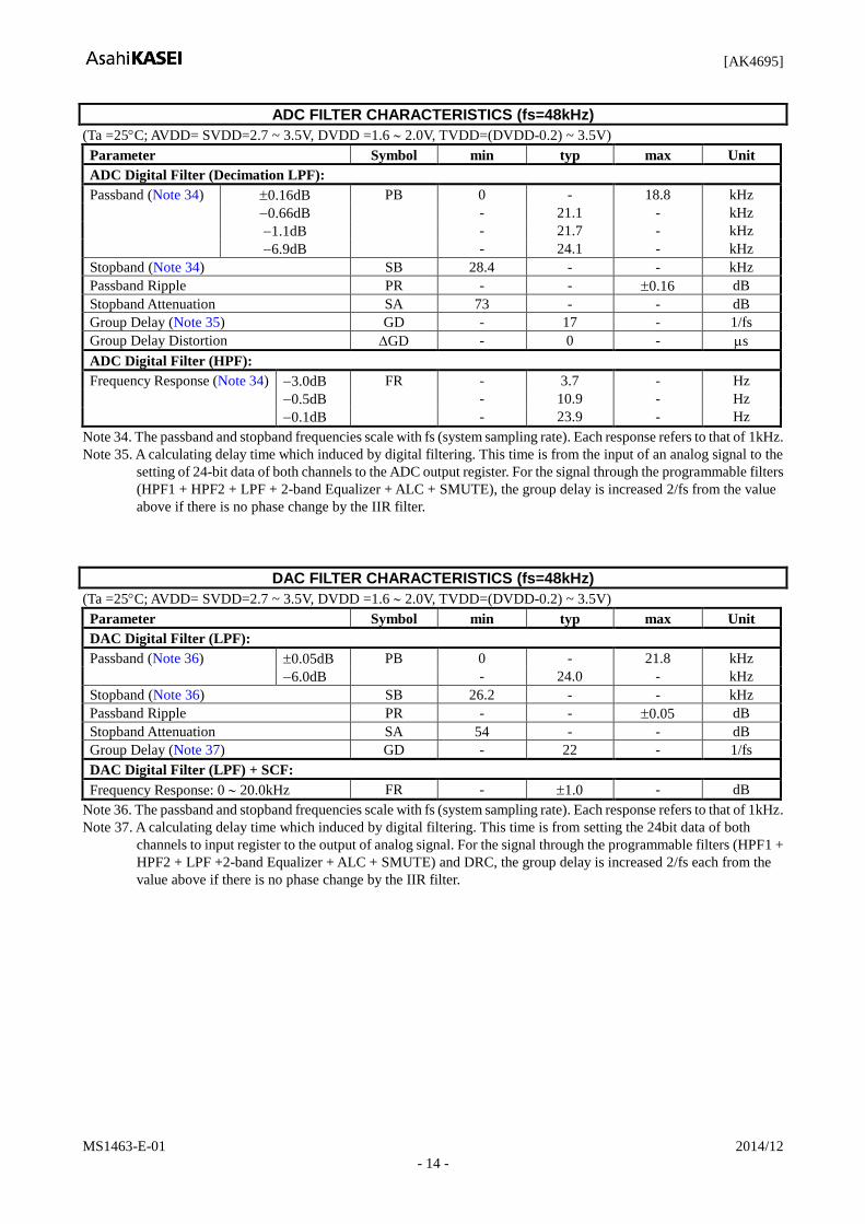
ADC FILTER CHARACTERISTICS (fs=48kHz)
(Ta =25C; AVDD= SVDD=2.7 ~ 3.5V, DVDD =1.6 2.0V, TVDD=(DVDD-0.2) ~ 3.5V)
Parameter Symbol min typ max Unit
ADC Digital Filter (Decimation LPF):
Passband (Note 34) 0.16dB PB 0 - 18.8 kHz
0.66dB - 21.1 - kHz
1.1dB - 21.7 - kHz
6.9dB - 24.1 - kHz
Stopband (Note 34) SB 28.4 - - kHz
Passband Ripple PR - - 0.16 dB
Stopband Attenuation SA 73 - - dB
Group Delay (Note 35) GD - 17 - 1/fs
Group Delay Distortion GD - 0 - s
ADC Digital Filter (HPF):
Frequency Response (Note 34) 3.0dB FR - 3.7 - Hz
0.5dB - 10.9 - Hz
0.1dB - 23.9 - Hz
Note 34. The passband and stopband frequencies scale with fs (system sampling rate). Each response refers to that of 1kHz.
Note 35. A calculating delay time which induced by digital filtering. This time is from the input of an analog signal to the
setting of 24-bit data of both channels to the ADC output register. For the signal through the programmable filters
(HPF1 + HPF2 + LPF + 2-band Equalizer + ALC + SMUTE), the group delay is increased 2/fs from the value
above if there is no phase change by the IIR filter.
DAC FILTER CHARACTERISTICS (fs=48kHz)
(Ta =25C; AVDD= SVDD=2.7 ~ 3.5V, DVDD =1.6 2.0V, TVDD=(DVDD-0.2) ~ 3.5V)
Parameter Symbol min typ max Unit
DAC Digital Filter (LPF):
Passband (Note 36) 0.05dB PB 0 - 21.8 kHz
6.0dB - 24.0 - kHz
Stopband (Note 36) SB 26.2 - - kHz
Passband Ripple PR - - 0.05 dB
Stopband Attenuation SA 54 - - dB
Group Delay (Note 37) GD - 22 - 1/fs
DAC Digital Filter (LPF) + SCF:
Frequency Response: 0 20.0kHz FR - 1.0 - dB
Note 36. The passband and stopband frequencies scale with fs (system sampling rate). Each response refers to that of 1kHz.
Note 37. A calculating delay time which induced by digital filtering. This time is from setting the 24bit data of both
channels to input register to the output of analog signal. For the signal through the programmable filters (HPF1 +
HPF2 + LPF +2-band Equalizer + ALC + SMUTE) and DRC, the group delay is increased 2/fs each from the
value above if there is no phase change by the IIR filter.

[AK4695]
MS1463-E-01 2014/12
- 15 -
DC CHARACTERISTICS
(Ta =25C; AVDD=SVDD=2.7 ~ 3.5V, DVDD =1.6 2.0V, TVDD=(DVDD-0.2) ~ 3.5V)
Parameter Symbol min typ max Unit
Audio Interface & Serial µP Interface (CSN, CDTIO, CCLK, PDN, BCKI, LRCK, SDTI, MCKI pins )
High-Level Input Voltage (TVDD ≥ 2.2V)
(TVDD < 2.2V)
Low-Level Input Voltage (TVDD ≥ 2.2V)
(TVDD < 2.2V)
VIH
VIL
70%TVDD
80%TVDD
-
-
-
-
-
-
-
-
30%TVDD
20%TVDD
V
V
V
V
Audio Interface & Serial µP Interface (CDTIO, SDTO1, SDTO2, GPO1 pins Output)
High-Level Output Voltage (Iout = 160A)
Low-Level Output Voltage (Iout = 160A)
VOH
VOL
TVDD0.2
-
-
-
-
0.2
V
V
Input Leakage Current Iin - - 10 A
Digital MIC Interface (DDAT0, DDAT1 pin Input ; DMIC bit = “1”)
High-Level Input Voltage
Low-Level Input Voltage
VIH2
VIL2
65%AVDD
-
-
-
-
35%AVDD
V
V
Digital MIC Interface (DMCLK pin Output ; DMIC bit = “1”)
High-Level Output Voltage (Iout = 160A)
Low-Level Output Voltage (Iout = 160A)
VOH2
VOL2
AVDD-0.4
-
-
-
-
0.4
V
V
Input Leakage Current Iin - - 10 A
[AK4695]
MS1463-E-01 2014/12
- 16 -
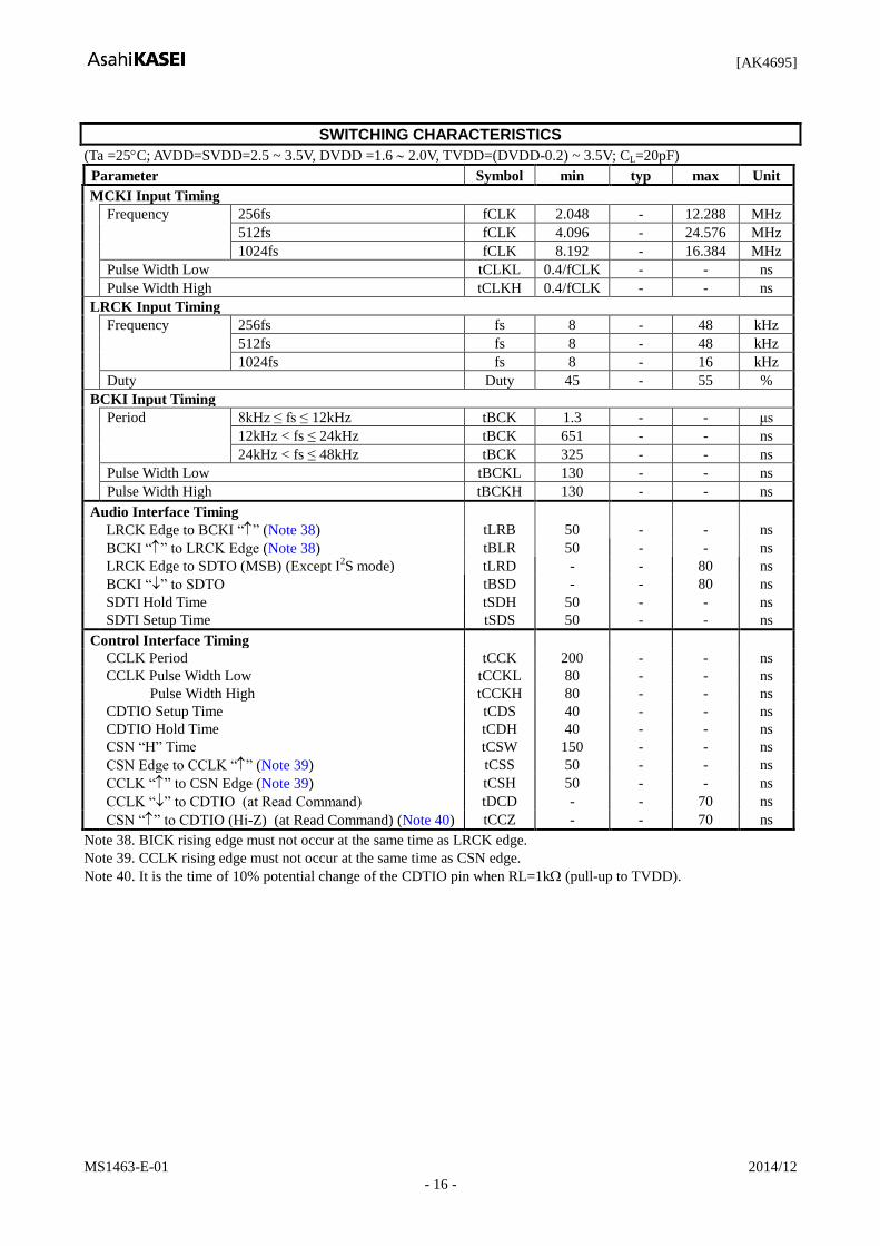
SWITCHING CHARACTERISTICS
(Ta =25C; AVDD=SVDD=2.5 ~ 3.5V, DVDD =1.6 2.0V, TVDD=(DVDD-0.2) ~ 3.5V; CL=20pF)
Parameter Symbol min typ max Unit
MCKI Input Timing
Frequency 256fs fCLK 2.048 - 12.288 MHz
512fs fCLK 4.096 - 24.576 MHz
1024fs fCLK 8.192 - 16.384 MHz
Pulse Width Low tCLKL 0.4/fCLK - - ns
Pulse Width High tCLKH 0.4/fCLK - - ns
LRCK Input Timing
Frequency 256fs fs 8 - 48 kHz
512fs fs 8 - 48 kHz
1024fs fs 8 - 16 kHz
Duty Duty 45 - 55 %
BCKI Input Timing
Period 8kHz ≤ fs ≤ 12kHz tBCK 1.3 - - μs
12kHz < fs ≤ 24kHz tBCK 651 - - ns
24kHz < fs ≤ 48kHz tBCK 325 - - ns
Pulse Width Low tBCKL 130 - - ns
Pulse Width High tBCKH 130 - - ns
Audio Interface Timing
LRCK Edge to BCKI “” (Note 38) tLRB 50 - - ns
BCKI “” to LRCK Edge (Note 38) tBLR 50 - - ns
LRCK Edge to SDTO (MSB) (Except I2S mode) tLRD - - 80 ns
BCKI “” to SDTO tBSD - - 80 ns
SDTI Hold Time tSDH 50 - - ns
SDTI Setup Time tSDS 50 - - ns
Control Interface Timing
CCLK Period tCCK 200 - - ns
CCLK Pulse Width Low tCCKL 80 - - ns
Pulse Width High tCCKH 80 - - ns
CDTIO Setup Time tCDS 40 - - ns
CDTIO Hold Time tCDH 40 - - ns
CSN “H” Time tCSW 150 - - ns
CSN Edge to CCLK “” (Note 39) tCSS 50 - - ns
CCLK “” to CSN Edge (Note 39) tCSH 50 - - ns
CCLK “” to CDTIO (at Read Command) tDCD - - 70 ns
CSN “” to CDTIO (Hi-Z) (at Read Command) (Note 40) tCCZ - - 70 ns
Note 38. BICK rising edge must not occur at the same time as LRCK edge.
Note 39. CCLK rising edge must not occur at the same time as CSN edge.
Note 40. It is the time of 10% potential change of the CDTIO pin when RL=1k (pull-up to TVDD).
[AK4695]
MS1463-E-01 2014/12
- 17 -
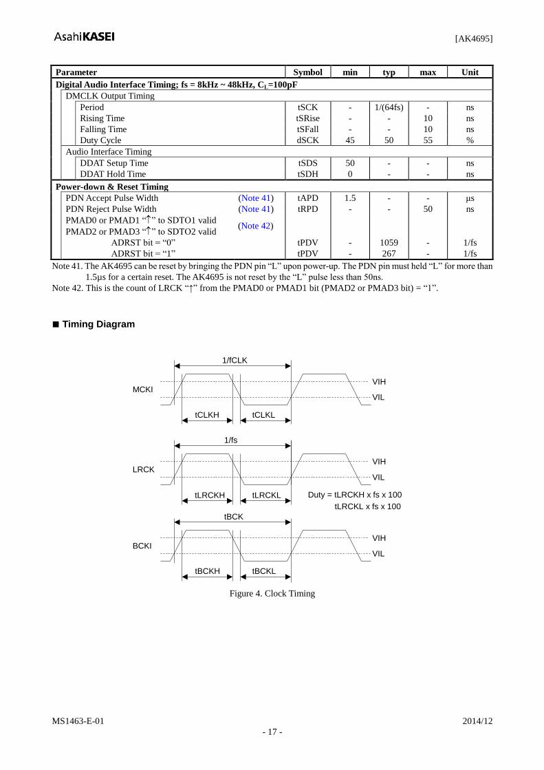
Parameter Symbol min typ max Unit
Digital Audio Interface Timing; fs = 8kHz ~ 48kHz, CL=100pF
DMCLK Output Timing
Period tSCK - 1/(64fs) - ns
Rising Time tSRise - - 10 ns
Falling Time tSFall - - 10 ns
Duty Cycle dSCK 45 50 55 %
Audio Interface Timing
DDAT Setup Time tSDS 50 - - ns
DDAT Hold Time tSDH 0 - - ns
Power-down & Reset Timing
PDN Accept Pulse Width (Note 41) tAPD 1.5 - - μs
PDN Reject Pulse Width (Note 41) tRPD - - 50 ns
PMAD0 or PMAD1 “” to SDTO1 valid
PMAD2 or PMAD3 “” to SDTO2 valid (Note 42)
ADRST bit = “0” tPDV - 1059 - 1/fs
ADRST bit = “1” tPDV - 267 - 1/fs
Note 41. The AK4695 can be reset by bringing the PDN pin “L” upon power-up. The PDN pin must held “L” for more than
1.5µs for a certain reset. The AK4695 is not reset by the “L” pulse less than 50ns.
Note 42. This is the count of LRCK “↑” from the PMAD0 or PMAD1 bit (PMAD2 or PMAD3 bit) = “1”.
Timing Diagram
1/fCLK
MCKI
tCLKH tCLKL
VIH
VIL
1/fs
LRCKVIH
VIL
tBCK
BCKI
tBCKH tBCKL
VIH
VIL
tLRCKH tLRCKL Duty = tLRCKH x fs x 100
tLRCKL x fs x 100
Figure 4. Clock Timing

[AK4695]
MS1463-E-01 2014/12
- 18 -
LRCKVIH
VIL
tBLR
BCKIVIH
VIL
tLRD
SDTO1
SDTO250%TVDD
tLRB
tBSD
tSDS
SDTIVIL
tSDH
VIH
MSB
Figure 5. Audio Interface Timing
CSNVIH
VIL
tCSS
CCLK
tCDS
VIH
VIL
CDTIOVIH
tCCKHtCCKL
tCDH
VILR/W A6 A5
tCCK
tCSH
Figure 6. WRITE Command Input Timing
CSNVIH
VIL
tCSH
CCLKVIH
VIL
CDTIOVIH
tCSW
VILD1 D0D2
tCSS
Figure 7. WRITE Data Input Timing

[AK4695]
MS1463-E-01 2014/12
- 19 -
CSN
CCLK
50% TVDD
CDTIO
VIH
D3 D2 D1 D0
tCCZ tDCD
VIL
VIH
VIL
Hi-Z
Clock, H or L
Figure 8. Read Data Output Timing
tSCK
65%AVDD
DMCLK
35%AVDD
tSCKL
50%AVDD
dSCK = 100 x tSCKL / tSCK
tSRise tSFall
Figure 9. DMCLK Clock Timing
DMCLK 65%AVDD
DDAT0 DDAT1
tSDS
VIH2
VIL2
tSDH
35%AVDD
Figure 30. Audio Interface Timing (DCLKP bit = “1”)
DMCLK 65%AVDD
DDAT0 DDAT1
tSDS
VIH2
VIL2
tSDH
35%AVDD
Figure 31. Audio Interface Timing (DCLKP bit = “0”)

[AK4695]
MS1463-E-01 2014/12
- 20 -
PMAD0/1/2/3 bits,
PMDM0/1/2/3 bits
tPDV
SDTO1
SDTO250%TVDD
Figure 10. Power Down & Reset Timing 1
tAPD
PDNVIL
tRPD
Figure 11. Power Down & Reset Timing 2

[AK4695]
MS1463-E-01 2014/12
- 21 -
OPERATION OVERVIEW
System Clock
The AK4695 operates on external slave mode. This mode is compatible with the interface of a normal audio CODEC.
Master clock can be input to the internal ADC and DAC directly from the MCKI pin without internal PLL circuit operation.
The external clocks required to operate the AK4695 are MCKI (256fs, 512fs or 1024fs), BCKI (32fs) and LRCK (fs).
The master clock (MCLK) must be synchronized with LRCK. The phase between these clocks is not important. Sampling
frequency and MCLK frequency can be selected by FS3-0 bits (Table 2).
Mode FS3 bit FS2 bit FS1 bit FS0 bit MCKI Input
Frequency Sampling Frequency Range
0 0 0 0 0
256fs
8kHz ≤ fs ≤ 16kHz
1 0 0 0 1 16kHz < fs ≤ 32kHz
2 0 0 1 0 32kHz < fs ≤ 48kHz (default)
4 0 1 0 0
512fs
8kHz ≤ fs ≤ 16kHz
5 0 1 0 1 16kHz < fs ≤ 32kHz
10 1 0 1 0 32kHz < fs ≤ 48kHz
12 1 1 0 0 1024s 8kHz ≤ fs ≤ 16kHz
Others Others N/A N/A
Table 2 MCKI Input Frequency and Sampling Frequency Setting
The S/N of the DAC at low sampling frequencies is worse than at high sampling frequencies due to out-of-band noise. The
out-of-band noise can be improved by using higher frequency of the master clock. The S/N of the DAC output through
LOUTA/ROUTA pins is shown in Table 3.
MCKI S/N
(fs=8kHz, 20kHzLPF + A-weighted)
Mode0: 256fs 80dB
Mode4: 512fs
Mode12: 1024fs 92dB
Table 3. Relationship between MCKI and S/N of LOUTA/ROUTA pins
AK4695 DSP or P
MCKI
BCKI
LRCK
SDTO1
SDTO2
BCLK
LRCK
SDTI1
SDTI2
1fs
32fs
MCLK
256fs, 512fs
or 1024fs
SDTI SDTO
Figure 12. EXT Slave Mode
[AK4695]
MS1463-E-01 2014/12
- 22 -
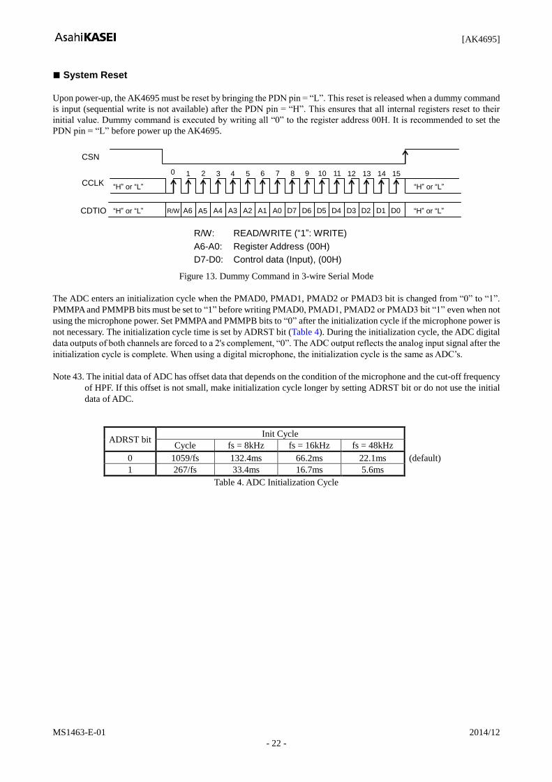
System Reset
Upon power-up, the AK4695 must be reset by bringing the PDN pin = “L”. This reset is released when a dummy command
is input (sequential write is not available) after the PDN pin = “H”. This ensures that all internal registers reset to their
initial value. Dummy command is executed by writing all “0” to the register address 00H. It is recommended to set the
PDN pin = “L” before power up the AK4695.
CSN
CCLK
0 1 2 3 4 5 6 7 8 9 10 11 12 13 14 15
CDTIO A6 A5 A2 A3 A1 A0 A4 D7 D6 D5 D4 D3 D2 D1 D0 R/W
R/W: READ/WRITE (“1”: WRITE)
A6-A0: Register Address (00H)
D7-D0: Control data (Input), (00H)
“H” or “L” “H” or “L”
“H” or “L” “H” or “L”
Figure 13. Dummy Command in 3-wire Serial Mode
The ADC enters an initialization cycle when the PMAD0, PMAD1, PMAD2 or PMAD3 bit is changed from “0” to “1”.
PMMPA and PMMPB bits must be set to “1” before writing PMAD0, PMAD1, PMAD2 or PMAD3 bit “1” even when not
using the microphone power. Set PMMPA and PMMPB bits to “0” after the initialization cycle if the microphone power is
not necessary. The initialization cycle time is set by ADRST bit (Table 4). During the initialization cycle, the ADC digital
data outputs of both channels are forced to a 2's complement, “0”. The ADC output reflects the analog input signal after the
initialization cycle is complete. When using a digital microphone, the initialization cycle is the same as ADC’s.
Note 43. The initial data of ADC has offset data that depends on the condition of the microphone and the cut-off frequency
of HPF. If this offset is not small, make initialization cycle longer by setting ADRST bit or do not use the initial
data of ADC.
ADRST bit Init Cycle
Cycle fs = 8kHz fs = 16kHz fs = 48kHz
0 1059/fs 132.4ms 66.2ms 22.1ms (default)
1 267/fs 33.4ms 16.7ms 5.6ms
Table 4. ADC Initialization Cycle

[AK4695]
MS1463-E-01 2014/12
- 23 -
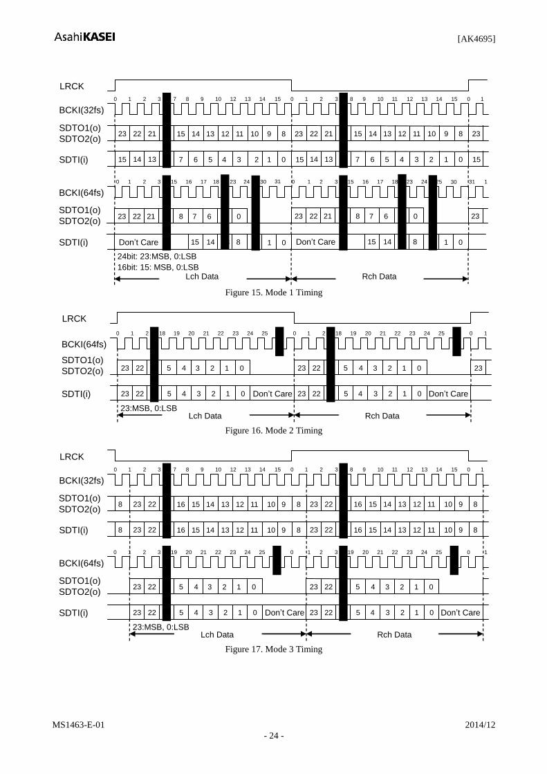
Audio Interface Format
Four types of data formats are available and selected by setting the DIF1-0 bits (Table 5). In all modes, the serial data is
MSB first, 2’s complement format. Audio interface formats can be used in both master and slave modes. The SDTO is
clocked out on the falling edge (“↓”) of BICK and the SDTI is latched on the rising edge (“↑”) of BICK.
Mode DIF1
bit
DIF0
bit
PFSEL
bit
SDTO1 (ADC1)
SDTO2 (ADC2) SDTI (DAC) BCKI Figure
0 0 0 x 24bit MSB justified 24bit LSB justified 48fs Figure 14
1 0 1 0
24bit MSB justified 16bit LSB justified 32fs
Figure 15
1 N/A (Note 44) 32fs
2 1 0 x 24bit MSB justified 24bit MSB justified 48fs Figure 16 (default)
3 1 1
0
I2S Compatible
I2S Compatible
=32fs or
48fs Figure 17
1 N/A (Note 44) 32fs
I2S Compatible 48fs
Note 44. When the path from SDTI to Programmable Filter is selected (PFSEL bit = “1”), do not select 16bit LSB justified
format (DIF1-0 bits = “01”) and I2S Compatible format (DIF1-0 bits = “11” when BCKI=32fs) of SDTI.
Table 5. Audio Interface Format (x: Don’t care, N/A: Not available)
If 24 or 16-bit data, the output of ADC, is converted to an 8-bit data by removing LSB 16 or 8-bit, “-1” data is converted to
“-1” of 8-bit data. And when the DAC playbacks this 8-bit data, “-1” of 8-bit data will be converted to “-65536” or
“-256”of 24 or 16-bit data which is a large offset. This offset can be removed by adding the offset of “32768” or “128” to
24 or 16-bit data, receptively before converting to 8-bit data.
LRCK
BCKI(64fs)
SDTO1(o)
SDTO2(o)
0 1 2 8 9 10 20 21 31 0 1 2 8 9 10 20 21 31 0
23
1
22 0 23 22 16 15 14 0 23
SDTI(i) 1 22 0 23 12 11 1 22 0 23 12 11
23:MSB, 0:LSB Lch Data Rch Data
Don’t Care Don’t Care
16 15 14
Figure 14. Mode 0 Timing
[AK4695]
MS1463-E-01 2014/12
- 24 -
LRCK
BCKI(64fs)
0 1 2 3 15 16 17 18 0 1 2 3 15 16 18 17 31 1
SDTI(i)
23 24 30 23 24 25
23 22 8
13 8 15 14
24bit: 23:MSB, 0:LSB
16bit: 15: MSB, 0:LSB Lch Data Rch Data
Don’t Care
21 5 0 7 6
BCKI(32fs)
0 1 2 3 7 8 9 10 0 1 2 3 15 9 11 10 0 1
SDTI(i)
12 13 14 12 13 14
22 21 22
3
21
2
10 8 23 9 15 14 13 12 11
15
23 10 8 9 15 14 13 12 11
8
23
14 13 14 13 2 0 15 1 7 6 5 4 3 15 2 0 1 7 6 5 4 3 15
0 2 1
31
23 22 8
13 8 15 14
21 5 0 7 6
0 2 1
30
Don’t Care
23
SDTO1(o)
SDTO2(o)
SDTO1(o)
SDTO2(o)
Figure 15. Mode 1 Timing
LRCK
BCKI(64fs)
SDTO1(o)
SDTO2(o)
0 1 2 18 19 20 21 22 0 1 2 18 19 20 22 21 0 1
SDTI(i)
23 24 25 23 24 25
23 22 4 23 22 5
4 5
4
1 22 0 23 3 2 1 22 0 23 3 2
23:MSB, 0:LSB Lch Data Rch Data
Don’t Care Don’t Care
5
5 4
1 0 3 2 1 0 3 2 23
Figure 16. Mode 2 Timing
LRCK
BCKI(64fs)
0 1 2 3 19 20 21 22 0 1 2 3 19 20 22 21 0 1
SDTI(i)
23 24 25 23 24 25
23 22 4 23 22 5
4 5
4
1 22 0 23 3 2 1 22 0 23 3 2
23:MSB, 0:LSB Lch Data Rch Data
Don’t Care Don’t Care
5
5 4
1 0 3 2 1 0 3 2
BCKI(32fs)
SDTO1(o)
SDTO2(o)
0 1 2 3 7 8 9 10 0 1 2 3 15 9 11 10 0 1
SDTI(i)
12 13 14 12 13 14
23 22 23 22 11 9 8 10 16 15 14 13 12
15
8 11 9 10 16 15 14 13 12
8
8
23 22 23 22 11 9 8 10 16 15 14 13 12 8 11 9 10 16 15 14 13 12 8
SDTO1(o)
SDTO2(o)
Figure 17. Mode 3 Timing

[AK4695]
MS1463-E-01 2014/12
- 25 -
Mono/Stereo Mode
PMAD1-0 and 3-2 bits set mono/stereo mode of ADC1 and ADC2 operation, respectively. When changing ADC operation
and analog/digital microphone, PMAD3-0 bits must be set “0” at first. When DMIC bit = “1”, PMAD3-0 bits settings are
ignored. When DMIC bit = “0”, PMDM3-0 bits settings are ignored. MMODE bit must be set to “1” (default: “0”) when
power up an ADC (PMADx bit = “1”).
PMAD0 bit PMAD1 bit ADC1 Lch data ADC1 Rch data
0 0 All “0” All “0” (default)
0 1 MIC1 Input Signal MIC1 Input Signal
1 0 MIC0 Input Signal MIC0 Input Signal
1 1 MIC0 Input Signal MIC1 Input Signal
Table 6. Mono/Stereo ADC1 operation (Analog MIC)
PMAD2 bit PMAD3 bit ADC2 Lch data ADC2 Rch data
0 0 All “0” All “0” (default)
0 1 MIC3 Input Signal MIC3 Input Signal
1 0 MIC2 Input Signal MIC2 Input Signal
1 1 MIC2 Input Signal MIC3 Input Signal
Table 7. Mono/Stereo ADC2 operation (Analog MIC)
PMDM0 bit PMDM1 bit ADC1 Lch data ADC1 Rch data
0 0 All “0” All “0” (default)
0 1 DMIC0 Rch Input Signal DMIC0 Rch Input Signal
1 0 DMIC0 Lch Input Signal DMIC0 Lch Input Signal
1 1 DMIC0 Lch Input Signal DMIC0 Rch Input Signal
Table 8. Mono/Stereo ADC1 operation (Digital MIC)
PMDM2 bit PMDM3 bit ADC1 Lch data ADC1 Rch data
0 0 All “0” All “0” (default)
0 1 DMIC1 Rch Input Signal DMIC1 Rch Input Signal
1 0 DMIC1 Lch Input Signal DMIC1 Lch Input Signal
1 1 DMIC1 Lch Input Signal DMIC1 Rch Input Signal
Table 9. Mono/Stereo ADC2 operation (Digital MIC)
[AK4695]
MS1463-E-01 2014/12
- 26 -
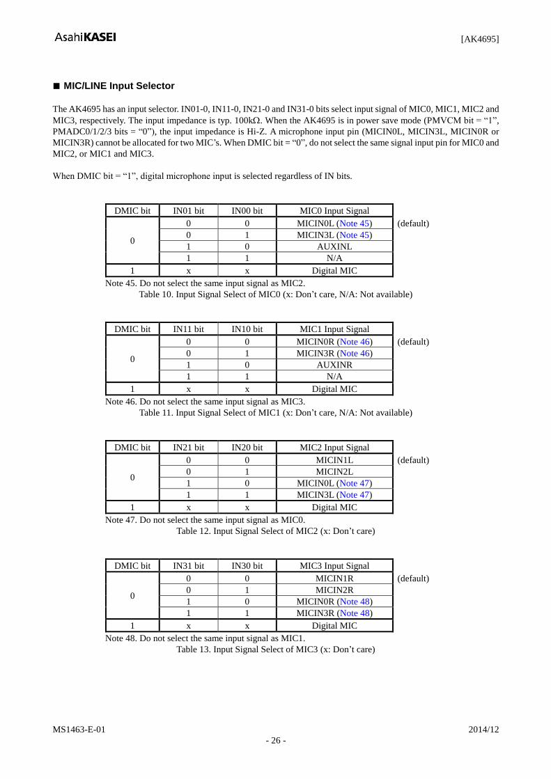
MIC/LINE Input Selector
The AK4695 has an input selector. IN01-0, IN11-0, IN21-0 and IN31-0 bits select input signal of MIC0, MIC1, MIC2 and
MIC3, respectively. The input impedance is typ. 100k. When the AK4695 is in power save mode (PMVCM bit = “1”,
PMADC0/1/2/3 bits = “0”), the input impedance is Hi-Z. A microphone input pin (MICIN0L, MICIN3L, MICIN0R or
MICIN3R) cannot be allocated for two MIC’s. When DMIC bit = “0”, do not select the same signal input pin for MIC0 and
MIC2, or MIC1 and MIC3.
When DMIC bit = “1”, digital microphone input is selected regardless of IN bits.
DMIC bit IN01 bit IN00 bit MIC0 Input Signal
0
0 0 MICIN0L (Note 45) (default)
0 1 MICIN3L (Note 45)
1 0 AUXINL
1 1 N/A
1 x x Digital MIC
Note 45. Do not select the same input signal as MIC2.
Table 10. Input Signal Select of MIC0 (x: Don’t care, N/A: Not available)
DMIC bit IN11 bit IN10 bit MIC1 Input Signal
0
0 0 MICIN0R (Note 46) (default)
0 1 MICIN3R (Note 46)
1 0 AUXINR
1 1 N/A
1 x x Digital MIC
Note 46. Do not select the same input signal as MIC3.
Table 11. Input Signal Select of MIC1 (x: Don’t care, N/A: Not available)
DMIC bit IN21 bit IN20 bit MIC2 Input Signal
0
0 0 MICIN1L (default)
0 1 MICIN2L
1 0 MICIN0L (Note 47)
1 1 MICIN3L (Note 47)
1 x x Digital MIC
Note 47. Do not select the same input signal as MIC0.
Table 12. Input Signal Select of MIC2 (x: Don’t care)
DMIC bit IN31 bit IN30 bit MIC3 Input Signal
0
0 0 MICIN1R (default)
0 1 MICIN2R
1 0 MICIN0R (Note 48)
1 1 MICIN3R (Note 48)
1 x x Digital MIC
Note 48. Do not select the same input signal as MIC1.
Table 13. Input Signal Select of MIC3 (x: Don’t care)
[AK4695]
MS1463-E-01 2014/12
- 27 -
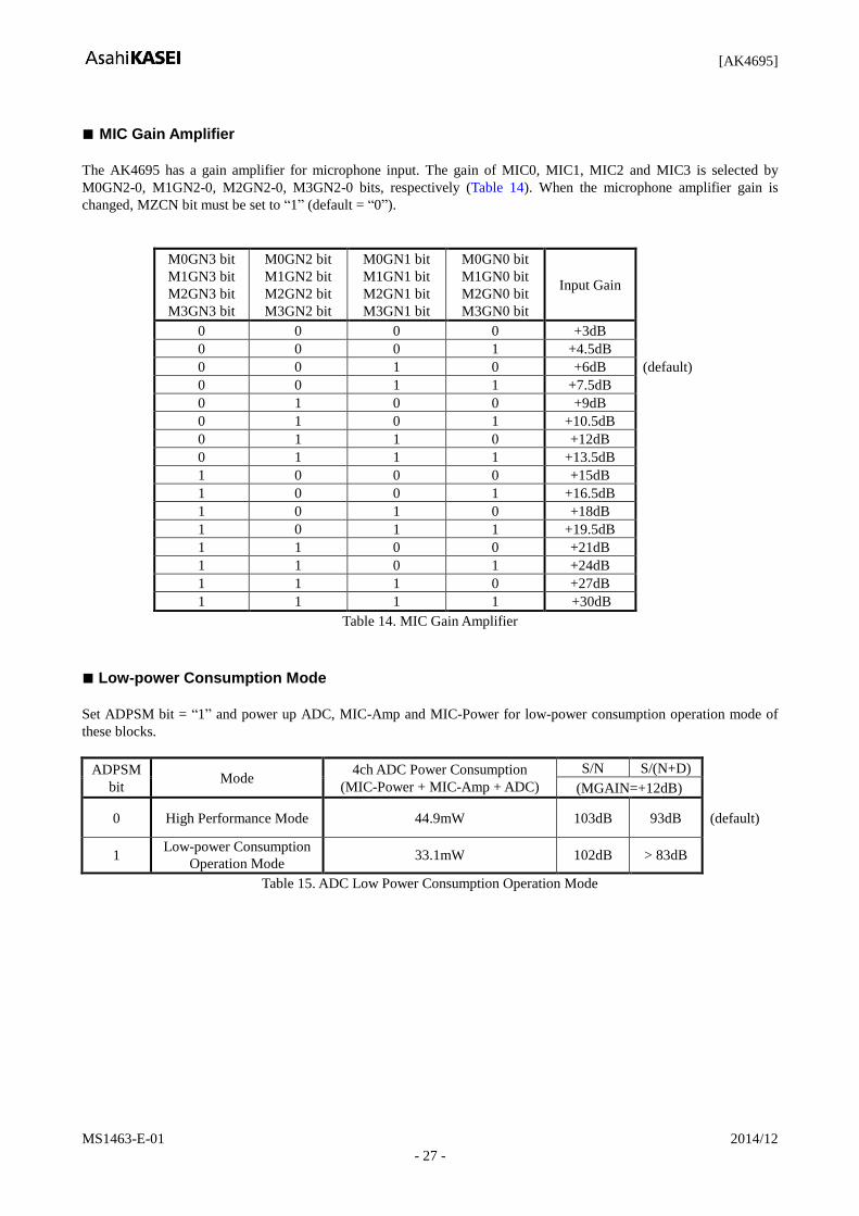
MIC Gain Amplifier
The AK4695 has a gain amplifier for microphone input. The gain of MIC0, MIC1, MIC2 and MIC3 is selected by
M0GN2-0, M1GN2-0, M2GN2-0, M3GN2-0 bits, respectively (Table 14). When the microphone amplifier gain is
changed, MZCN bit must be set to “1” (default = “0”).
M0GN3 bit
M1GN3 bit
M2GN3 bit
M3GN3 bit
M0GN2 bit
M1GN2 bit
M2GN2 bit
M3GN2 bit
M0GN1 bit
M1GN1 bit
M2GN1 bit
M3GN1 bit
M0GN0 bit
M1GN0 bit
M2GN0 bit
M3GN0 bit
Input Gain
0 0 0 0 +3dB
0 0 0 1 +4.5dB
0 0 1 0 +6dB (default)
0 0 1 1 +7.5dB
0 1 0 0 +9dB
0 1 0 1 +10.5dB
0 1 1 0 +12dB
0 1 1 1 +13.5dB
1 0 0 0 +15dB
1 0 0 1 +16.5dB
1 0 1 0 +18dB
1 0 1 1 +19.5dB
1 1 0 0 +21dB
1 1 0 1 +24dB
1 1 1 0 +27dB
1 1 1 1 +30dB
Table 14. MIC Gain Amplifier
Low-power Consumption Mode
Set ADPSM bit = “1” and power up ADC, MIC-Amp and MIC-Power for low-power consumption operation mode of
these blocks.
ADPSM
bit Mode
4ch ADC Power Consumption
(MIC-Power + MIC-Amp + ADC)
S/N S/(N+D)
(MGAIN=+12dB)
0 High Performance Mode 44.9mW 103dB 93dB (default)
1 Low-power Consumption
Operation Mode 33.1mW 102dB > 83dB
Table 15. ADC Low Power Consumption Operation Mode

[AK4695]
MS1463-E-01 2014/12
- 28 -
MIC Power
When PMMPA/B bit = “1”, the MPWRA/B pin supplies power for the microphones. This output voltage is typically 2.4V
(0.857 x AVDD) and the load resistance is minimum 250 for the MPWRA pin and minimum 500 for the MPWRB pin.
Any capacitor must not be connected directly to the MPWRA and MPWRB pins (Figure 18).
MIC power can be switched ON/OFF regardless of the ADC status. However, the voltage at the microphone input pin will
be shifted and need time to return to the VCOM voltage when power up the MIC power during the ADC is powered on.
This recovery time to the VOCM voltage is dependent on the capacitance of the input capacitor and the time constant of the
input impedance.
PMMPA bit MPWRA pin
0 Hi-Z (default)
1 Output
Table 16. Output Setting of MIC Power A
PMMPB bit MPWRB pin
0 Hi-Z (default)
1 Output
Table 17. Output Setting of MIC Power B
MPWRA pin
2
k
MIC Power
Microphone
MICIN0L pin
Microphone
Microphone
Microphone
2
k
2
k
2
k
MPWRB pin
“PMMPB”
“PMMPA”
Microphone
Microphone
Microphone
Microphone
1
k
1
k
1
k
1
k
MICIN0R pin
MICIN1L pin
MICIN1R pin
MICIN2L pin
MICIN2R pin
MICIN3L pin
MICIN3R pin
Figure 18. MIC Block Circuit
[AK4695]
MS1463-E-01 2014/12
- 29 -
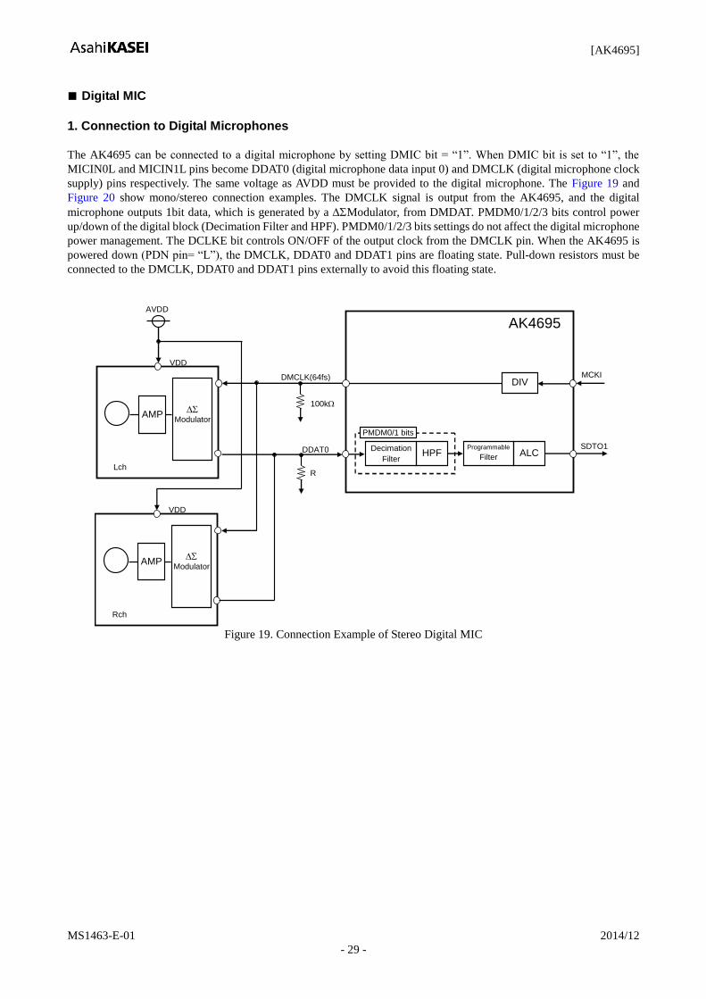
Digital MIC
1. Connection to Digital Microphones
The AK4695 can be connected to a digital microphone by setting DMIC bit = “1”. When DMIC bit is set to “1”, the
MICIN0L and MICIN1L pins become DDAT0 (digital microphone data input 0) and DMCLK (digital microphone clock
supply) pins respectively. The same voltage as AVDD must be provided to the digital microphone. The Figure 19 and
Figure 20 show mono/stereo connection examples. The DMCLK signal is output from the AK4695, and the digital
microphone outputs 1bit data, which is generated by a Modulator, from DMDAT. PMDM0/1/2/3 bits control power
up/down of the digital block (Decimation Filter and HPF). PMDM0/1/2/3 bits settings do not affect the digital microphone
power management. The DCLKE bit controls ON/OFF of the output clock from the DMCLK pin. When the AK4695 is
powered down (PDN pin= “L”), the DMCLK, DDAT0 and DDAT1 pins are floating state. Pull-down resistors must be
connected to the DMCLK, DDAT0 and DDAT1 pins externally to avoid this floating state.
AMP
Modulator
DDAT0
DMCLK(64fs)
Decimation
Filter
DIV MCKI
ALC SDTO1 Programmable
Filter
VDD
AK4695 AVDD
100k
R
AMP
Modulator
VDD
Lch
Rch
HPF
PMDM0/1 bits
Figure 19. Connection Example of Stereo Digital MIC

[AK4695]
MS1463-E-01 2014/12
- 30 -
AMP
Modulator
DDAT0
DMCLK(64fs)
Decimation
Filter
DIV MCKI
ALC
SDTO1 Programmable
Filter
VDD
AK4695 AVDD
100k
R
AMP
Modulator
VDD
L0ch
R0ch
HPF
AMP
Modulator
VDD
AMP
Modulator
VDD
L1ch
R1ch
Decimation
Filter
Programmable
Filter HPF SDTO2
DDAT1
R
PMDM2/3 bits
PMDM0/1 bits
Figure 20. Connection Example of 4ch Digital MIC

[AK4695]
MS1463-E-01 2014/12
- 31 -
2. Interface
The input data channel of the DDAT0 and DDAT1 pins are set by DCLKP bit. When DCLKP bit = “1, Lch data is input to
the decimation filter if the DMCLK pin= “H”, and Rch data is input if the DMCLK pin= “L”. When DCLKP bit = “0”, Rch
data is input to the decimation filter if the DMCLK pin= “H”, and Lch data is input if the DMCLK pin= “L”. The DMCLK
pin outputs “L” when DCLKE bit = “0”, and only supports 64fs. In this case, necessary clocks must be supplied to the
AK4695 for ADC operation. The output data through the Decimation and Digital Filters is 24bit full scale when the 1bit
data density is 0%~100%.
DCLKP bit DMCLK = “H” DMCLK = “L”
0 Rch Lch (default)
1 Lch Rch
Table 18. Data Input/Output Timing with Digital MIC
DMCLK(64fs)
DDAT0 (Lch) DDAT1 (Lch)
Valid Data
Valid Data
Valid Data
Valid Data
DDAT0 (Rch) DDAT1 (Rch)
Valid Data
Valid Data
Valid Data
Valid Data
Figure 21. Data Input/Output Timing with Digital MIC (DCLKP bit = “1”)
DMCLK(64fs)
Valid Data
Valid Data
Valid Data
Valid Data
Valid Data
Valid Data
Valid Data
Valid Data
DDAT0 (Lch) DDAT1 (Lch)
DDAT0 (Rch) DDAT1 (Rch)
Figure 22. Data Input/Output Timing with Digital MIC (DCLKP bit = “0”)

[AK4695]
MS1463-E-01 2014/12
- 32 -
Digital Block
The digital block consists of the blocks shown in Figure 23. Recording path and playback path is selected by setting PFSEL
bit, PFSDO bit and DASEL1-0 bits. (Figure 24 ~ Figure 27, Table 19) PMDSP bit = “1” powers up the whole
programmable filter block. PMWNG and PMPFILx bits control the each block individually.
DACA
1st Order
HPFA
ADCA
DVLA SMUTEA
SDTO2
PFSEL bit
1st Order
HPF2
SDTO2
HPF20-21 bits
HPFAD bit
PMDSP bit
PMDACA bit
PMAD0/1 bits or PMDM0/1 bits
LPF10-11 bits
ALC0-3 bits
SMUTE SMUTE bit
PFSDO bit
1st Order
LPF1
PMDRC bit
DRC
DRCENA bit
1st Order
HPFB
ADCB
HPFAD bit
PMAD2/3 bits or PMDM2/3 bits
ALC (Volume)
1st Order
HPF2
HPF22-23 bits
LPF12-13 bits 1st Order
LPF1
Gain Adj. Gain Adj.
“0” “1”
“0” “1” “0” “1”
SDTO1
To Line Outputs
DACB
DVLB SMUTEB
To HP or SPK
PMDACB bit
“0” “1” “0” “1”
SEL DASEL1-0 bits
SDTO1
SDTI
DRCENB bit
1st Order
HPF1
HPF10-11 bits 1st Order
HPF1
HPF12-13 bits
2 Band
EQ1-2
EQ10-11 bits
EQ20-21 bits
2 Band
EQ1-2
EQ12-13 bits
EQ22-23 bits
PMPFIL0-1 bits PMPFIL2-3 bits
PMPFIL0 or PMPFIL1 or PMPFIL2 or
PMPFIL3 bits
(1) ADCA/B: Includes the Digital Filter (LPF) for ADC as shown in “FILTER CHRACTERISTICS”.
(2) HPFA/B: Digital Filter (HPF) for ADC as shown in “FILTER CHRACTERISTICS”.
(3) Gain Adj.: Applicable for use as MIC sensitivity correction.
(4) HPF1/2: High Pass Filter. Applicable for use as Wind-Noise Reduction Filter. (See “Digital Programmable Filter
Circuit”)
(5) LPF1: Low Pass Filter (See “Digital Programmable Filter Circuit”)
(6) 2-Band EQ: Applicable for use as Equalizer or Notch Filter. (See “Digital Programmable Filter Circuit”)
(7) Volume: Input Digital Volume with ALC function. (See “Input Digital Volume” and “ALC Operation”)
(8) SMUTE: Soft Mute Function (See “Digital Programmable Filter Circuit”)
(9) DRC: Dynamic range control circuit for playback path. (See “DRC Operation”)
(10) DVLA/B: Digital volume with soft mute function for playback path (See “Output Digital Volume” )
(11) DACA/B: Includes the Digital Filter (LPF) for DAC as shown is “FILTER CHARACTERISTICS”
Figure 23. Digital Block Path Select

[AK4695]
MS1463-E-01 2014/12
- 33 -
Mode PFSEL bit DASEL1-0
bits PFSDO bit
DRCENA bit
DRCENB bit Figure
Recording Mode 1 & Playback Mode 2 0 00 1 0 Figure 24
Recording Mode 2 & Playback Mode 1 1 01 1 0 Figure 25
Recording Mode 2 & Playback Mode 2
(Programmable Filter Bypass Mode:
PMDSP bit = “0”)
X 00 0 1 Figure 26
Loopback Mode 0 01 or 10 1 0 Figure 27
Table 19. Recording Playback Mode (x: Don’t care)
HPF10-3, HPF20-3, LPF10-3, EQ10-3, EQ20-3 and ALC0-3 bits must be “0” when changing those modes.
DACA/B
1st Order
HPF2
ADCA/B 2 Band
EQ
ALC (Volume)
DVLA/B SMUTEA/B
1st Order
LPF1
SMUTE 1st Order
HPFA/B
MIC Gain Adjust
1st Order
HPF1
Figure 24. Path at Recording Mode 1 & Playback Mode 2 (default)
DACA/B 1st Order
HPF2
ADCA/B
2 Band
EQ
ALC (Volume)
DVLA/B SMUTEA/B 1st Order
LPF1
SMUTE
1st Order
HPFA/B
MIC Gain Adjust
1st Order
HPF1
Figure 25. Path at Recording Mode 2 & Playback Mode 1
DACA/B
ADCA/B
DVLA/B SMUTEA/B
1st Order
HPFA/B
DRC
MIC Gain Adjust
Figure 26. Path at Recording Mode 2 & Playback Mode 2
DACA/B
1st Order
HPF2
ADCA/B 2 Band
EQ
ALC (Volume)
DVLA/B SMUTEA/B
1st Order
LPF1
SMUTE 1st Order
HPFA/B
MIC Gain Adjust
1st Order
HPF1
Figure 27. Path at Loopback Mode

[AK4695]
MS1463-E-01 2014/12
- 34 -
Digital HPFA/B
Digital High Pass Filters (HPFA and HPFB) are integrated for DC offset cancellation of the ADC input. The cut-off
frequency of the HPFA/B is proportional to the sampling frequency (fs) and the default is 3.7Hz (@fs = 48kHz). HPFAD
bit controls the ON/OFF of the HPFA/B (ON is recommended). HPFAD bit must be changed when PMAD3-0 bits = “0”
MIC Sensitivity Correction
The AK4695 has microphone sensitivity correction function controlled by M1ADJ3-0 bits, M2ADJ3-0 bits and
M3ADJ3-0 bits.
M0ADJ3-0, M1ADJ3-0 bits
M2ADJ3-0, M3ADJ3-0 bits GAIN (dB) Step
0000 0 (default)
0001 –0.75
0010 –1.5
0011 –2.25
0100 –3.0
0101 –3.75
0110 –4.5 0.75dB
0111 –5.25
1000 –6.0
1001 –6.75
1010 –7.5
1011 –8.25
1100 –9.0
Others N/A
Table 20. MIC Sensitivity Correction (N/A: Not available)

[AK4695]
MS1463-E-01 2014/12
- 35 -
Digital Programmable Filter Circuit
SMUTE
HPF10
HPF11
HPF12
HPF13
HPF20
HPF21
HPF22
HPF23
LPF10
LPF11
LPF12
LPF13
EQ10
EQ11
EQ12
EQ13
EQ20
EQ21
EQ22
EQ23
ALC0
ALC1
ALC2
ALC3
SMTM
SDTO0
SDTO1
PMPFIL0 bit
PMPFIL1 bit
PMPFIL2 bit
PMPFIL3 bit
PMPFIL0 or PMPFIL1 or PMPFIL2 or PMPFIL3 bits
Ch0
Ch1
Ch2
Ch3
HPF1A13-0 HPF1B13-0
LPF1A13-0 LPF1B13-0
E1A15-0 E1B15-0 E1C15-0
E2A15-0 E2B15-0 E2C15-0
ALC3-0
Figure 28. Programmable Filter Circuit
(1) High Pass Filter (HPF1, HPF2)
Normally, this HPF is used for Wind-Noise Reduction. This is composed two 1st order HPFs. The coefficient of HPF1 and
HPF2 are set by HPF1A13-0 bits and HPF1B13-0 bits. The coefficient setting is common for all channels of HPF1 and
HPF2. HPF10-13 bits and HPF20-23 bits control ON/OFF of the HPF1 and HPF2, respectively. When the HPF1 and
HPF2 are OFF, the audio data passes this block by 0dB gain. The coefficient must be set when HPF10-13= HPF20-23 bits
= “0”, PMDSP bit = “0” or PMPFIL3-0 bits = “0”. The HPF1 and HPF2 start operation 4/fs (max) after when HPF1x
=HPF2x bit=PMPFIL bit= PMDSP bit = “1” is set. Each channel can be powered down individually by PMPFIL3-0 bits.
The powered-down channel by PMPFIL3-0 bits outputs “0”.
fs: Sampling Frequency
fc: Cut-off Frequency
Register Setting (Note 49)
HPF1, HPF2: HPF1A[13:0] bits =A, HPF1B[13:0] bits =B
(MSB=HPF1A13, HPF1B13; LSB=HPF1A0, HPF1B0)
A =
1 / tan (fc/fs)
1 + 1 / tan (fc/fs)
B =
1 1 / tan (fc/fs)
1 + 1 / tan (fc/fs)
,
Transfer function
H(z) = A
1 z 1
1 + Bz 1
The cut-off frequency must be set as below.
fc/fs 0.0001 (fc min = 4.8Hz at 48 kHz)

[AK4695]
MS1463-E-01 2014/12
- 36 -
(2) Low Pass Filter (LPF1)
This is composed with 1st order LPF. LFP1A13-0 bits and LFP1B13-0 bits set the coefficient of LPF. This coefficient
setting is common for all channels. LPF13-10 bit controls ON/OFF of the each channel. When the LPF1 is OFF, the audio
data passes this block by 0dB gain. The coefficient must be set when LPF13-10 bits = “0”, PMPFIL3-0 bits = “0” or
PMDSP bit = “0”. The LPF1 starts operation 4/fs(max) after when LPF1x bit =PMPFIL bit= PMDSP bit = “1” is set. Each
channel can be powered down individually by PMPFIL3-0 bits. The powered-down channel by PMPFFIL3-0 bits outputs
“0”.
fs: Sampling frequency
fc: Cut-off frequency
Register setting (Note 49)
LPF1: LPF1A[13:0] bits =A, LPF1B[13:0] bits =B
(MSB= LPF1A13, LPF1B13; LSB= LPF1A0, LPF1B0)
A =
1
1 + 1 / tan (fc/fs)
B =
1 1 / tan (fc/fs)
1 + 1 / tan (fc/fs)
,
Transfer function
H(z) = A
1 + z 1
1 + Bz 1
The cut-off frequency must be set as below.
fc/fs 0.05 (fc min = 2400Hz at 48kHz)
(3) 2-band Equalizer
This block can be used as Equalizer or Notch Filter. A 2-band Equalizer (EQ1 and EQ2) is switched ON/OFF
independently by EQ13-10 and EQ23-20 bits. When the Equalizer is OFF, the audio data passes this block by 0dB gain.
The calculating delay time does not differ on each channel whether the equalizer is ON or OFF.
E1A15-0, E1B15-0 and E1C15-0 bits set the coefficient of EQ1. E2A15-0, E2B15-0 and E2C15-0 bits set the coefficient
of EQ2. The coefficient setting is common for all channels. The EQx (x=12) coefficient must be set when EQx bit = “0”
or PMPFIL3-0 bits = “0”. EQ1-2 start operation 4/fs(max) after when EQx (x=1~5) = PMPFIL = PMDSP bit = “1”is set.
Each channel can be powered down individually by PMPFIL3-0 bits. The powered-down channel by PMPFIL3-0 bits
outputs “0”.
fs: Sampling frequency
fo1 ~ fo2: Center frequency
fb1 ~ fb2: Band width where the gain is 3dB different from center frequency
K1 ~ K2 : Gain ( -1 Kn < 3 )
Register setting (Note 49)
EQ1: E1A[15:0] bits =A1, E1B[15:0] bits =B1, E1C[15:0] bits =C1
EQ2: E2A[15:0] bits =A2, E2B[15:0] bits =B2, E2C[15:0] bits =C2
(MSB=E1A15, E1B15, E1C15, E2A15, E2B15, E2C15 ; LSB= E1A0, E1B0, E1C0, E2A0, E2B0, E2C0)

[AK4695]
MS1463-E-01 2014/12
- 37 -
An = Kn x
tan (fbn/fs)
1 + tan (fbn/fs)
Bn = cos(2 fon/fs) x
2
1 + tan (fbn/fs)
, Cn =
1 tan (fbn/fs)
1 + tan (fbn/fs) ,
(n = 1, 2)
Transfer function
hn (z) = An
1 z 2
1 Bnz 1 Cnz
2
H(z) = 1 + h1(z) + h2(z)
(n = 1, 2) The center frequency must be set as below.
0.003 < fon / fs < 0.497
When gain of K is set to “-1”, this equalizer becomes a notch filter. When EQ1 EQ2 is used as a notch filter, central
frequency of a real notch filter deviates from the above-mentioned calculation, if its central frequency of each band is near.
The control software that is attached to the evaluation board has functions that revises a gap of frequency and calculates the
coefficient. When its central frequency of each band is near, the central frequency should be revised and confirm the
frequency response.
Note 49. [[Translation the filter coefficient calculated by the equations above from real number to binary code (2’s
complement)]
X = (Real number of filter coefficient calculated by the equations above) x 213
X must be rounded to integer, and then should be translated to binary code (2’s complement).
MSB of each filter coefficient setting register is sign bit.
The power consumption can be reduced by setting HPF1, HPF2, LPF, EQ1 or EQ2 off while either PMPFIL2 or PMPFIL3
bit is “0”, or either PMPFIL0 or PMPFIL1bit is “0”.

[AK4695]
MS1463-E-01 2014/12
- 38 -
ALC Operation
The ALC (Automatic Level Control) is operated by ALC block when ALC bit is “1”. When PFSEL bit is “0”, ALC circuit
operates at recording path. When PFSEL bit is “1”, ALC circuit operates at playback path. The calculating delay time does
not differ on each channel whether ALC is ON or OFF. ALC block is powered up when PMDSP bit= PMPFILx bits=
ALCx bits = “1”. Each channel can be powered down individually by PMPFIL3-0 bits. The powered-down channel by
PMPFFIL3-0 bits outputs “0” data.
The ALC block consists of these blocks shown below. ALC limiter detection level and ALC recovery wait counter reset
level are monitored at Level Detection 2 block after EQ block. The Level Detection 1 block also monitors clipping
detection level (+0.53dBFS).
Volume
ALC Control
Level Detection 2 EQ
Input
Output
Level Detection 1
Figure 29. ALC Block
The polar (fc1) and zero-point (fc2) frequencies of EQ block are dependent on the sampling frequency. The coefficient is
changed automatically according to the sampling frequency range setting. When ALC EQ block is OFF (ALCEQ bit = “1”),
these level detection are off.
Sampling Frequency Range Polar Frequency (fc1) Zero-point Frequency (fc2)
8kHz fs 16kHz
(FS3-2 bits = “11”) 150Hz 100Hz fs=12kHz
8kHz fs 32kHz
(FS3-2 bits = “01”) 150Hz 100Hz fs=24kHz
8kHz fs 48kHz
(FS3-2 bits = “00”) 150Hz 100Hz fs=48kHz
32kHz < fs 48kHz
(FS3-2 bits = “10”)
Table 21. ALCEQ Frequency Setting
fs: Sampling Frequency
fc1: Polar Frequency
fc2: Zero-point Frequency
A = 10K/20
x
1 + 1 / tan (fc2/fs)
1 + 1 / tan (fc1/fs)
B =
1 1 / tan (fc1/fs)
1 + 1 / tan (fc1/fs)
,
1 1 / tan (fc2/fs)
1 + 1 / tan (fc1/fs)
, C = 10K/20
x
Transfer function
H(z) =
A + Cz 1
1 + Bz 1

[AK4695]
MS1463-E-01 2014/12
- 39 -
[ ALCEQ: First order zero pole high pass filter ]
Gain [dB]
0dB
100Hz (fc2)
150Hz (fc1)
Frequency [Hz]
-3.5dB
Figure 30. ALCEQ Frequency Response (fs = 48kHz)
1. ALC Limiter Operation
During ALC limiter operation, when either L or R channel output level exceeds the ALC limiter detection level (Table 22),
the VOL value (same value for both L and R) is attenuated automatically according to the output level (Table 23). The
volume is attenuated by the step amount shown in Table 23 at every sampling. (This attenuation is repeated for sixteen
times once ALC limiter operation is executed.)
After completing the attenuate operation, unless ALC0/1/2/3 bit is changed to “0”, the operation repeats when the input
signal level exceeds ALC limiter detection level.
When ATTLMT bit = “1”, VOL value is attenuated to 0dB if the volume is over ALC limiter detection level. In this case,
attenuation under 0dB is not executed. The reference level must be set to a plus value or mute. When ATTLMT bit = “0”
(default values), normal attenuation is executed without volume limitation.
LMTH1 bit LMTH0 bit ALC Limiter Detection Level
(LM-LEVEL)
ALC Recovery Waiting Counter
Reset Level
0 0 –2.5dBFS –4.1dBFS (default)
0 1 –4.1dBFS –6.0dBFS
1 0 –6.0dBFS –8.5dBFS
1 1 –8.5dBFS –12dBFS
Table 22. ALC Limiter Detection Level / Recovery Counter Reset Level
Output Level ATT Step [dB]
+0.53dBFS Output Level (Level Detection 1) 0.38148
–1.16dBFS EQ Output Level (Level Detection 2) < +0.53dBFS 0.06812
LM-LEVEL EQ Output Level (Level Detection 2) < –1.16dBFS 0.02548
Table 23. ALC Limiter ATT Amount
[AK4695]
MS1463-E-01 2014/12
- 40 -
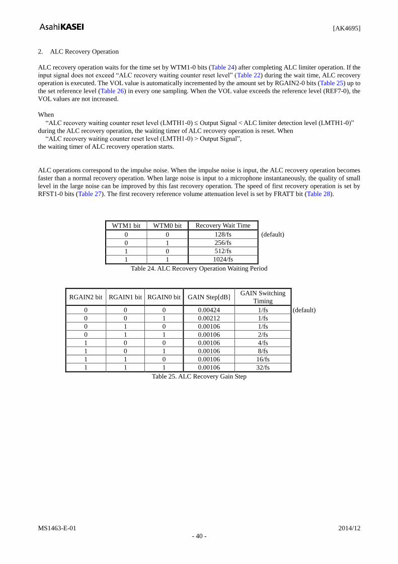
2. ALC Recovery Operation
ALC recovery operation waits for the time set by WTM1-0 bits (Table 24) after completing ALC limiter operation. If the
input signal does not exceed “ALC recovery waiting counter reset level” (Table 22) during the wait time, ALC recovery
operation is executed. The VOL value is automatically incremented by the amount set by RGAIN2-0 bits (Table 25) up to
the set reference level (Table 26) in every one sampling. When the VOL value exceeds the reference level (REF70), the
VOL values are not increased.
When
“ALC recovery waiting counter reset level (LMTH1-0) Output Signal < ALC limiter detection level (LMTH1-0)”
during the ALC recovery operation, the waiting timer of ALC recovery operation is reset. When
“ALC recovery waiting counter reset level (LMTH1-0) > Output Signal”,
the waiting timer of ALC recovery operation starts.
ALC operations correspond to the impulse noise. When the impulse noise is input, the ALC recovery operation becomes
faster than a normal recovery operation. When large noise is input to a microphone instantaneously, the quality of small
level in the large noise can be improved by this fast recovery operation. The speed of first recovery operation is set by
RFST1-0 bits (Table 27). The first recovery reference volume attenuation level is set by FRATT bit (Table 28).
WTM1 bit WTM0 bit Recovery Wait Time
0 0 128/fs (default)
0 1 256/fs
1 0 512/fs
1 1 1024/fs
Table 24. ALC Recovery Operation Waiting Period
RGAIN2 bit RGAIN1 bit RGAIN0 bit GAIN Step[dB] GAIN Switching
Timing
0 0 0 0.00424 1/fs (default)
0 0 1 0.00212 1/fs
0 1 0 0.00106 1/fs
0 1 1 0.00106 2/fs
1 0 0 0.00106 4/fs
1 0 1 0.00106 8/fs
1 1 0 0.00106 16/fs
1 1 1 0.00106 32/fs
Table 25. ALC Recovery Gain Step

[AK4695]
MS1463-E-01 2014/12
- 41 -
REF7-0 bits GAIN [dB] Step
F0H +54.0
0.375 dB
EFH +53.625
EEH +53.25
: :
B0H +30.0 (default)
: :
61H +0.375
60H 0.0
5FH –0.375
: :
02H –35.25
01H –35.625
00H MUTE
Table 26. Reference Level at ALC Recovery Operation
RFST1-0 bits First Recovery Gain Step
[dB]
00 0.0032 (default)
01 0.0042
10 0.0064
11 0.0127
Table 27. ALC First Recovery Gain Step
FRATT bit ATT Amount
(dB)
ATT Switch
Timing
0 -0.00106 4/fs (default)
1 -0.00106 16/fs
Table 28. ALC First Recovery Reference Volume ATT Step
[AK4695]
MS1463-E-01 2014/12
- 42 -
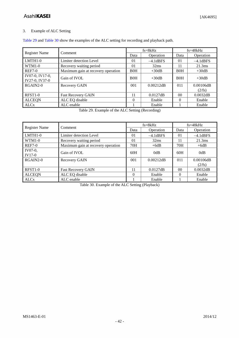
3. Example of ALC Setting
Table 29 and Table 30 show the examples of the ALC setting for recording and playback path.
Register Name Comment fs=8kHz fs=48kHz
Data Operation Data Operation
LMTH1-0 Limiter detection Level 01 4.1dBFS 01 4.1dBFS
WTM1-0 Recovery waiting period 01 32ms 11 21.3ms
REF7-0 Maximum gain at recovery operation B0H +30dB B0H +30dB
IV07-0, IV17-0,
IV27-0, IV37-0 Gain of IVOL B0H +30dB B0H +30dB
RGAIN2-0 Recovery GAIN 001 0.00212dB 011 0.00106dB
(2/fs)
RFST1-0 Fast Recovery GAIN 11 0.0127dB 00 0.0032dB
ALCEQN ALC EQ disable 0 Enable 0 Enable
ALCx ALC enable 1 Enable 1 Enable
Table 29. Example of the ALC Setting (Recording)
Register Name Comment fs=8kHz fs=48kHz
Data Operation Data Operation
LMTH1-0 Limiter detection Level 01 4.1dBFS 01 4.1dBFS
WTM1-0 Recovery waiting period 01 32ms 11 21.3ms
REF7-0 Maximum gain at recovery operation 70H +6dB 70H +6dB
IV07-0,
IV17-0 Gain of IVOL 60H 0dB 60H 0dB
RGAIN2-0 Recovery GAIN 001 0.00212dB 011 0.00106dB
(2/fs)
RFST1-0 Fast Recovery GAIN 11 0.0127dB 00 0.0032dB
ALCEQN ALC EQ disable 0 Enable 0 Enable
ALCx ALC enable 1 Enable 1 Enable
Table 30. Example of the ALC Setting (Playback)

[AK4695]
MS1463-E-01 2014/12
- 43 -
4. Example of registers set-up sequence of ALC Operation
The following registers must not be changed during ALC operation. These bits must be changed after ALC operation is
finished by ALC3-0 bits = “0”. The reference level can be changed during ALC operation. If the reference level is reduced
the volume level is changed by soft transition in 0.02548dB/fs step. The volume is also changed by soft transition to the
IVOL setting value (IVx7-0 bits) until manual mode starts after ALCx bit is set to “0”. Do not change the REF value during
soft transition when REF7-0 bits are set to 00H (MUTE).
When changing ALC operation channels, finish all ALC operations at first (ALC3-0 bits = “0”) and write ALCx bit = “1”.
In this case, ALCx bit writing must be made with an interval of 2/fs. It is recommended that ALC operation is enabled after
transition time since the volume changes to the IVOL setting value by soft transition when ALC operation is finished.
The reference volume and IVOL should be set to a value more than 0dB or mute when ATTLMT bit = “1”. Do not set
ATTLMT bit to “1” during the soft transition of when changing the REF value from 0dB or more to MUTE and vice versa.
LMTH1-0, WTM1-0, RFST1-0, ATTLMT and ALCEQN bits
Manual Mode
* The value of IVx should be
the same or smaller than REF’s
WR (IVx7-0)
WR (REF7-0)
WR (LMTH1-0, WTM 1-0, RGAIN2-0 RFST1-0, ATTLMT, ALCEQN)
Example:
Recovery Wait Time = 21.3ms@48kHz
Recovery Quantity = 0.00106dB (2/fs)
Fast Recovery Quantity = 0.0032 dB
Maximum Gain = +30.0dB
Limiter Detection Level = 4.1dBFS
ALCx bit = “1”
(2) Addr=0AH-0DH, Data=B0H
(1) Addr=09H, Data=B0H
(3) Addr=14H, Data=3DH Addr=15H, Data=00H
ALC Operation
WR (ALCx = “1”) (4) Addr=17H, Data=F0H
Figure 31. Registers Set-up Sequence in ALC Operation (recording path)

[AK4695]
MS1463-E-01 2014/12
- 44 -
Input Digital Volume (Manual Mode)
The input digital volume becomes manual mode by setting ALC bit = “0”. This mode is suitable in the cases shown below.
1. After exiting reset state, when setting up the registers for ALC operation (such as LMTH bit and etc.)
2. When changing registers for ALC operation (Limiter period, Recovery period and etc.) due to sampling
frequency change.
3. When IVOL is used as a manual volume control.
IV07-0, IV17-0, IV27-0 and IV37-0 bits set the gain of the digital input volume (Table 31). Ch0, Ch1, Ch2 and Ch3
volumes are set individually by IV07-0, IV17-0, IV27-0 and IV37-0 bits, respectively. The volume change between set
values are executed by soft transition in 0.09375dB/fs. Therefore no switching noise occurs during the transition. It takes
960/fs (20ms@fs=48kHz) from F0H(+54dB) to 00H(MUTE).
IV07-0 bits
IV17-0 bits
IV27-0 bits
IV37-0 bits
GAIN [dB] Step
F0H +54.0
0.375 dB
EFH +53.625
EEH +53.25
: :
B0H +30.0 (default)
: :
61H +0.375
60H 0.0
5FH –0.375
: :
02H –35.25
01H –35.625
00H MUTE
Table 31. Input Digital Volume Setting
If IV07-0, IV17-0, IV27-0 or IV37-0 bits are written during PMDSP bit or PMPFIL3-0 bits = “0”, IVOL operation starts
with the written values after PMPFIL3/2/1/0 bit is changed to “1” while PMDSP bit = “1”.

[AK4695]
MS1463-E-01 2014/12
- 45 -
Soft Mute
Soft mute operation is performed in the digital domain. When the SMUTE bit is set “1”, the output signal is attenuated to
-∞ (“0”) after attenuated to -59.5dB, during the cycle set by SMTM bit. When the SMUTE bit is returned to “0”, the mute
status (-∞dB) is cancelled and the output attenuation level gradually changes to 0dB from -59dB during the cycle set by
SMTM bit. If the soft mute is cancelled within the cycle set by SMTM bit after starting the operation, the attenuation is
discontinued and the attenuation level returns to 0dB.
The mute status (-∞dB) is held by setting PMDSP bit = “1” and PMPFILx bit = “1” after setting SMUTE bit = “1” while
PMDSP bit = “0” and PMPFIL3-0 bits = “0”, unless changing SMUTE bit to “0”. In case of changing the SMUTE bit
setting within 2/fs after setting PMPFIL bit to “1” while PMDSP bit = “1”, the programmable filter block is powered up in
mute status if SMUTE bit = “1”, and it is powered up in IVOL setting value if SMUTE bit = “0”.
PMPFILx bit should not be changed during soft mute transition.
SMTM bit ATT Level Transition Time from 0dB to
Setting fs=8kHz fs=48kHz
0 240/fs 30ms 5ms
1 480/fs 60ms 10ms (default)
Table 32. Output Digital Volume Transition Time Setting
SMUTE bit
Attenuation Level
0dB
-
(1) (2)
(1)
SMTM bit
SMTM bit
-59.5dB
Figure 32. Soft Mute Function
(1) The input signal is attenuated by (“0”) during the cycle set by SMTM bit.
(2) If soft mute is cancelled within the cycle set by SMTM bit after starting the operation, the attenuation is discounted and
the attenuation level returns to 0dB within the same cycle.
[AK4695]
MS1463-E-01 2014/12
- 46 -
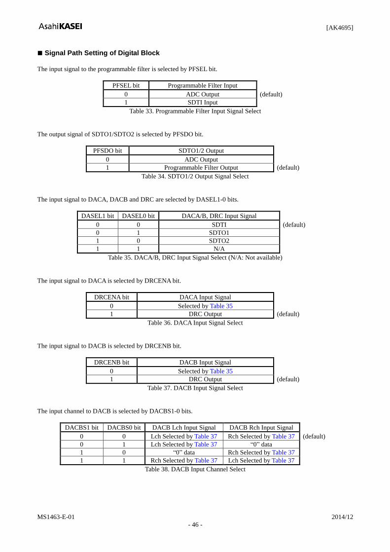
Signal Path Setting of Digital Block
The input signal to the programmable filter is selected by PFSEL bit.
PFSEL bit Programmable Filter Input
0 ADC Output (default)
1 SDTI Input
Table 33. Programmable Filter Input Signal Select
The output signal of SDTO1/SDTO2 is selected by PFSDO bit.
PFSDO bit SDTO1/2 Output
0 ADC Output
1 Programmable Filter Output (default)
Table 34. SDTO1/2 Output Signal Select
The input signal to DACA, DACB and DRC are selected by DASEL1-0 bits.
DASEL1 bit DASEL0 bit DACA/B, DRC Input Signal
0 0 SDTI (default)
0 1 SDTO1
1 0 SDTO2
1 1 N/A
Table 35. DACA/B, DRC Input Signal Select (N/A: Not available)
The input signal to DACA is selected by DRCENA bit.
DRCENA bit DACA Input Signal
0 Selected by Table 35
1 DRC Output (default)
Table 36. DACA Input Signal Select
The input signal to DACB is selected by DRCENB bit.
DRCENB bit DACB Input Signal
0 Selected by Table 35
1 DRC Output (default)
Table 37. DACB Input Signal Select
The input channel to DACB is selected by DACBS1-0 bits.
DACBS1 bit DACBS0 bit DACB Lch Input Signal DACB Rch Input Signal
0 0 Lch Selected by Table 37 Rch Selected by 104HTable 37 (default)
0 1 Lch Selected by Table 37 “0” data
1 0 “0” data Rch Selected by 104HTable 37
1 1 Rch Selected by Table 37 Lch Selected by Table 37
Table 38. DACB Input Channel Select

[AK4695]
MS1463-E-01 2014/12
- 47 -
Dynamic Range Control
Noise Suppression
NSLPF NSLA13-0 NSLB13-0
NSHPF NSHA13-0 NSHB13-0
HPF
NSCE NSTHL4-0 NSTHH4-0 NSREF3-0 NSATT2-0
NSGAIN2-0 NSIAFS1-0 NSOAFS1-0
DRC Block
LPF HPF Mono/ Stereo
DRCM1-0
LPF
LPF
HPF
VOLM
VOLL
VOLH
DVLCL
DVLCM
DVLCH
VOL DRC Limiter
PMDRC
DHHPF1-0 DHHA13-0 DHHB13-0
DLLPF1-0 DLLA13-0 DLLB13-0
DMLPF1-0 DMLA13-0 DMLB13-0
DMHPF1-0 DMHA13-0 DMHB13-0
VL1X/Y5-0 VL2X/Y5-0 VL3X/Y4-0
L1G6-0 L2G6-0 L3G6-0
L4G6-0
DAF1-0 DVLMAT2-0 DVRGAIN2-0
VM1X/Y5-0 VM2X/Y5-0 VM3X/Y4-0
M1G6-0 M2G6-0 M3G6-0 M4G6-0
VH1X/Y5-0 VH2X/Y5-0 VH3X/Y4-0
H1G6-0 H2G6-0 H3G6-0 H4G6-0
DRCC1-0
DACA
DLMAT1-0 DRGAIN1-0
DVLA SMUTEA
DACB DVLB
SMUTEB
Figure 33. DRC Functions and Signal Path
DRCM1-0 bits select stereo or mono of DRC input data. In case of mono mode, the same data is input to both L and R
channels.
DRCM1 bit DRCM0 bit Lch Rch
0 0 L R (default)
0 1 L L
1 0 R R
1 1 N/A
Table 39. DRC Stereo/Mono Select (N/A: Not Available)
1. Noise Suppression Block
(1) Low Pass Filter (LPF) This is composed with 1st order LPF. NSLA13-0 bits and NSLB13-0 bits set the coefficient of LPF. NSLPF bit controls
ON/OFF of the LPF. When the LPF is OFF, the audio data passes this block by 0dB gain. The coefficient must be set when
NSLPF bit = “0” or PMDRC bit = “0”. The LPF starts operation 4/fs (max) after when NSLPF bit = “1” or PMDRC bit =
“1” are set.
fs: Sampling Frequency
fc: Cut-off frequency
Register setting
LPF: NSLA[13:0] bits =A, NSLB[13:0] bits =B
(MSB=NSLA13, NSLB13; LSB=NSLA0, NSLB0)
A =
1
1 + 1 / tan (fc/fs)
B =
1 1 / tan (fc/fs)
1 + 1 / tan (fc/fs)
,
Transfer function
H(z) = A
1 + z 1
1 + Bz 1
The cut-off frequency should be set as below.
fc/fs 0.05 (fc min = 2400Hz at 48kHz)

[AK4695]
MS1463-E-01 2014/12
- 48 -
(2) High Pass Filter (HPF) This is composed 1st order HPF. The coefficient of HPF is set by NSHA13-0 bits and NSHB13-0 bits. NSHPF bit controls
ON/OFF of the HPF. When the HPF is OFF, the audio data passes this block by 0dB gain. The coefficient must be set when
NSHPF bit = “0” or PMDRC bit = “0”. The HPF starts operation 4/fs (max) after when NSHPF bit = “1” or PMDRC bit =
“1” is set.
fs: Sampling frequency
fc: Cut-off frequency
Register setting
HPF: NSHA[13:0] bits =A, NSHB[13:0] bits =B
(MSB=NSHA13, NSHB13; LSB=NSHA0, NSHB0)
A =
1 / tan (fc/fs)
1 + 1 / tan (fc/fs)
B =
1 1 / tan (fc/fs)
1 + 1 / tan (fc/fs)
,
Transfer function
H(z) = A
1 z 1
1 + Bz 1
The cut-off frequency should be set as below.
fc/fs 0.0001 (fc min = 4.8Hz at 48kHz)
(3) Noise Suppression
The Noise Suppression is enabled when NSCE bit (Noise suppression enable bit) = “1” during DRC operation (PMDRC
bit = “1”). This function attenuates output signal level automatically when minute amount of the signal is input.
NSCE bit: Noise Suppression Enable
0: Disable (default)
1: Enable
(3-1) Noise Level Suppressing Operation
The output signal is suppressed when the input moving average level set by NSIAF1-0 bits (Table 40) is lower than “Noise
Suppression Threshold Low Level” set by NSTHL4-0 bits (Table 41) during the normal operation.
This operation attenuates the volume automatically to the reference level set by NSREF3-0 bits (Table 42) with the soft
transition of the attenuation speed set by NSATT2-0 bits (Table 43).
NSIAF1-0 bits Moving Average Parameter
fs=8kHz fs=16kHz fs=48kHz
00 256/fs 32ms 16ms 5.3ms
01 512/fs 64ms 32ms 10.7ms
10 1024/fs 128ms 64ms 21.3ms (default)
11 2048/fs 256ms 128ms 42.7ms
Table 40. Input Signal moving Average Parameter Setting (Normal Operation )
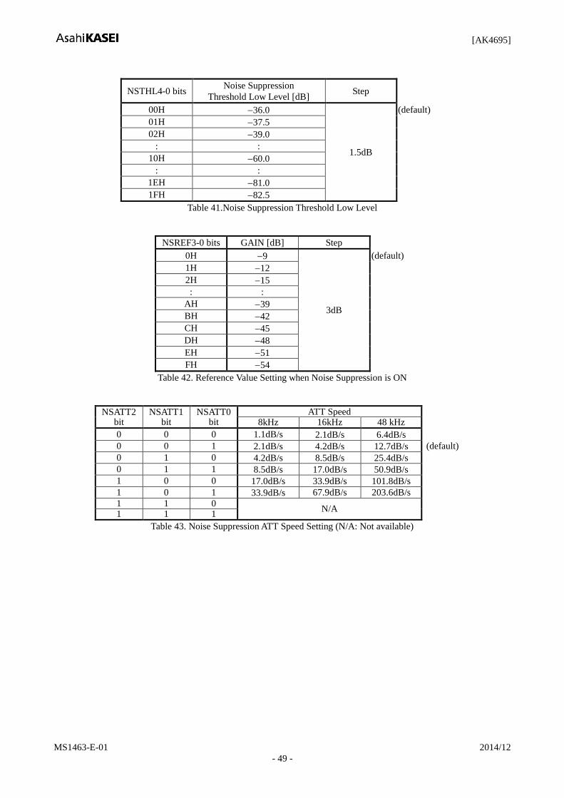
[AK4695]
MS1463-E-01 2014/12
- 49 -
NSTHL4-0 bits Noise Suppression
Threshold Low Level [dB] Step
00H 36.0
1.5dB
(default)
01H 37.5
02H 39.0
: :
10H 60.0
: :
1EH 81.0
1FH 82.5
Table 41.Noise Suppression Threshold Low Level
NSREF3-0 bits GAIN [dB] Step
0H 9
3dB
(default)
1H 12
2H 15
: :
AH 39
BH 42
CH 45
DH 48
EH 51
FH 54
Table 42. Reference Value Setting when Noise Suppression is ON
NSATT2 bit
NSATT1 bit
NSATT0 bit
ATT Speed 8kHz 16kHz 48 kHz
0 0 0 1.1dB/s 2.1dB/s 6.4dB/s
0 0 1 2.1dB/s 4.2dB/s 12.7dB/s (default)
0 1 0 4.2dB/s 8.5dB/s 25.4dB/s
0 1 1 8.5dB/s 17.0dB/s 50.9dB/s
1 0 0 17.0dB/s 33.9dB/s 101.8dB/s
1 0 1 33.9dB/s 67.9dB/s 203.6dB/s
1 1 0 N/A
1 1 1
Table 43. Noise Suppression ATT Speed Setting (N/A: Not available)

[AK4695]
MS1463-E-01 2014/12
- 50 -
(3-2) Noise Suppression → Normal Operation
During noise suppressing operation, if the input moving average level set by NSOAF1-0 bits (Table 44) exceeds Noise
Suppression Threshold High Level set by NSTHH4-0 bits (Table 45), the operation switches to normal operation from
noise suppressing operation.
This recovery operation sets the volume automatically to 0dB with the soft transition of the recovery speed set by
NSGAIN2-0 bits (Table 46).
NSOAF1-0 bits Moving Average Parameter
fs=8kHz fs=16kHz fs=48kHz
00 4/fs 0.5ms 0.3ms 0.1ms
01 8/fs 1.0ms 0.5ms 0.2ms
10 16/fs 2.0ms 1.0ms 0.3ms (default)
11 32/fs 4.0ms 2.0ms 0.7ms
Table 44. Moving Average Parameter Setting at Noise Suppression On
NSTHH4-0 bits Noise Suppression
Threshold High Level [dB] Step
00H 36.0
1.5dB
(default)
01H 37.5
02H 39.0
: :
10H 60.0
: :
1EH 81.0
1FH 82.5
Table 45.Noise Suppression Threshold High Level
NSGAIN2 bit
NSGAIN1 bit
NSGAIN0 bit
Recovery Speed 8kHz 16kHz 48kHz
0 0 0 0.3dB/ms 0.5dB/ms 1.6dB/ms
0 0 1 0.5dB/ms 1.1dB/ms 3.3dB/ms (default)
0 1 0 1.1dB/ms 2.2dB/ms 6.6dB/ms
0 1 1 2.2dB/ms 4.4dB/ms 13.2dB/ms
1 0 0 4.5dB/ms 9.0dB/ms 26.9dB/ms
1 0 1 N/A
1 1 0 1 1 1
Table 46. Recovery Speed Setting from Noise Suppression to Normal Operation (N/A: Not available)

[AK4695]
MS1463-E-01 2014/12
- 51 -
2. Dynamic Volume Control Block
The AK4695 has the dynamic volume control (DVLC) circuits before DRC. DVLC divides frequency range into three
band (Low, Middle and High) and controls independently. To set characteristics of the DVLC circuit around flat, it is
recommended that the cutoff frequencies of the LPF for Low Frequency Rage is set to the same value of cutoff frequency
of HPF for Middle Frequency Range, and the cutoff frequency of LPF for Middle Frequency Range is set to the same value
of cutoff frequency of HPF for High Frequency Range when using first order LPF and HFP. When using second order
filters, the cutoff frequency of the LPF for Low Frequency Range should be set to the value which is four times than the
HPF for Middle Frequency Range, and the cutoff frequency of the LPF for Middle Frequency Range should be set to the
value which is four times than the HPF for High Frequency Range.
(1) Low Frequency Range
LPF VOLL DVLCL
DLLPF1-0 DLLA13-0 DLLB13-0
VL1X/Y5-0 VL2X/Y5-0 VL3X/Y4-0
L1G6-0 L2G6-0 L3G6-0 L4G6-0
“0” data (DLLPF1-0 bits = “00”)
Figure 34. DVLC Functions and Signal Path for Low Frequency Range
(1-1) Low Pass Filter (LPF)
This is composed with 1st or 2nd order LPF. DLLA13-0 bits and DLLB13-0 bits set the coefficient of LPF. DLLPF1-0 bits
controls ON/OFF of the LPF. When the LPF is OFF, the audio data does not pass this block. The coefficient must be set
when DLLPF1-0 bits = “00” or PMDRC bit = “0”. The LPF starts operation 4/fs(max) after when DLLPF1-0 bits = “01”
or “10” and PMDRC bit = “1” are set.
DLLPF1 bit DLLPF0 bit Mode
0 0 OFF (“0” data) (default)
0 1 1st order LPF
1 0 2nd order LPF
1 1 N/A
Table 47. DLLPF Mode Setting (N/A: Not Available)
fs: Sampling frequency
fc: Cut-off frequency
Register setting
LPF: DLLA[13:0] bits =A, DLLB[13:0] bits =B
(MSB=DLLA13, DLLB13; LSB=DLLA0, DLLB0)
A =
1
1 + 1 / tan (fc/fs)
B =
1 1 / tan (fc/fs)
1 + 1 / tan (fc/fs)
,
Transfer function (1st order)
H(z) = A
1 + z 1
1 + Bz 1

[AK4695]
MS1463-E-01 2014/12
- 52 -
Transfer function (2nd order)
H(z) = A
1 + z 1
1 + Bz 1
x A
1 + z 1
1 + Bz 1
The cut-off frequency should be set as below.
fc/fs 0.002 (fc min = 96Hz at 48kHz)
(1-2) Dynamic Volume Control Curve
The inflection points of the DVLC curve is set by three coordinate values (VL1X5-0, VL1Y5-0, VL2X5-0, VL2Y5-0,
VL3X4-0 and VL3Y4-0 bits). The setting of three inflection points are calculated the values of (X1L, Y1L), (X2L, Y2L),
(X3L, Y3L) in dB. The inflection points should be set in such a way that VL1X ≤ VL2X ≤ VL3X, VL1Y ≤ VL2Y ≤ VL3Y.
And the each slope is set by L1G6-0, L2G6-0, L3G6-0 and L4G6-0 bits. X4L is fixed full-scale, Y4L is calculated by the
L4G value. The initial value of the DVLC gain is set by the L1G.
Full scale DVLC Input Level
DV
LC
Outp
ut Level
Full scale
L1G
L2G
L4G
L3G
(0, 0)
(X1L, Y1L)
(X2L, Y2L)
(X3L, Y3L) (X4L, Y4L)
Figure 35. DVLC Curve for Low Frequency Range
VL1X/Y5-0 bits
VL2X/Y5-0 bits
Dynamic Volume Control Point
[dB] Step
00H 0
1.5dB
(default)
01H 1.5
02H 3.0
: :
2EH 69.0
2FH 70.5
30H N/A
N/A
: :
3FH N/A
Table 48. DVLC Point Setting for X/Y1, X/Y2 (N/A: Not available)
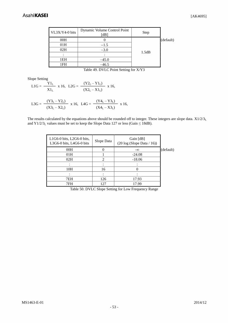
[AK4695]
MS1463-E-01 2014/12
- 53 -
VL3X/Y4-0 bits Dynamic Volume Control Point
[dB] Step
00H 0
1.5dB
(default)
01H 1.5
02H 3.0
: :
1EH 45.0
1FH 46.5
Table 49. DVLC Point Setting for X/Y3
Slope Setting
L1G = Y1L
X1L x 16,
L2G = (Y2L – Y1L)
(X2L – X1L) x 16,
L3G = (Y3L – Y2L)
(X3L – X2L) x 16,
L4G = (Y4L – Y3L)
(X4L – X3L) x 16,
The results calculated by the equations above should be rounded off to integer. These integers are slope data. X1/2/3L
and Y1/2/3L values must be set to keep the Slope Data 127 or less (Gain ≤ 18dB).
L1G6-0 bits, L2G6-0 bits,
L3G6-0 bits, L4G6-0 bits Slope Data
Gain [dB]
(20 log (Slope Data / 16))
00H 0 -∞ (default)
01H 1 -24.08
02H 2 -18.06
: : :
10H 16 0
: : :
7EH 126 17.93
7FH 127 17.99
Table 50. DVLC Slope Setting for Low Frequency Range

[AK4695]
MS1463-E-01 2014/12
- 54 -
(2) Middle Frequency Range
HPF LPF VOLM DVLCM
DMLPF1-0 DMLA13-0 DMLB13-0
DMHPF1-0 DMHA13-0 DMHB13-0
VM1X/Y5-0 VM2X/Y5-0 VM3X/Y4-0
M1G6-0 M2G6-0 M3G6-0 M4G6-0
Bypass (DMHPF1-0 = DMLPF1-0 bits = “00”)
Figure 36. DVLC Functions and Signal Path for Middle Frequency Range
(2-1) High Pass Filter (HPF) This is composed with 1st or 2nd order HPF. The coefficient of HPF is set by DMHA13-0 bits and DMHB13-0 bits. HPF
bit controls ON/OFF of the HPF. When the HPF is OFF, the audio data passes this block by 0dB gain. The coefficient must
be set when DMHPF1-0 bits = “00” or PMDRC bit = “0”. The HPF starts operation 4/fs(max) after when DMHPF1-0 bits
= “01” or “10” and PMDRC bit = “1” are set.
DMHPF1 bit DMHPF0 bit Mode
0 0 Bypass (default)
0 1 1st order HPF
1 0 2nd order HPF
1 1 N/A
Table 51. DMHPF Mode Setting (N/A: Not Available)
fs: Sampling frequency
fc: Cut-off frequency
Register setting
HPF: DMHA[13:0] bits =A, DMHB[13:0] bits =B
(MSB=DMHA13, DMHB13; LSB=DMHA0, DMHB0)
A =
1 / tan (fc/fs)
1 + 1 / tan (fc/fs)
B =
1 1 / tan (fc/fs)
1 + 1 / tan (fc/fs)
,
Transfer function (1st order)
H(z) = A
1 z 1
1 + Bz 1
Transfer function (2nd order)
H(z) = A
1 z 1
1 + Bz 1
x A
1 z 1
1 + Bz 1
The cut-off frequency should be set as below.
fc/fs 0.0001 (fc min = 4.8Hz at 48kHz)

[AK4695]
MS1463-E-01 2014/12
- 55 -
(2-2) Low Pass Filter (LPF) This is composed with 1st or 2nd order LPF. DMLA13-0 bits and DMLB13-0 bits set the coefficient of LPF. DMLPF1-0
bits controls ON/OFF of the LPF. When the LPF is OFF, the audio data passes this block by 0dB gain. The coefficient must
be set when DMLPF1-0 bits = “00” or PMDRC bit = “0”. The LPF starts operation 4/fs(max) after when DMLPF1-0 bits
= “01” or “10” and PMDRC bit = “1” are set.
DMLPF1 bit DMLPF0 bit Mode
0 0 Bypass (default)
0 1 1st order LPF
1 0 2nd order LPF
1 1 N/A
Table 52. DMLPF Mode Setting (N/A: Not Available)
fs: Sampling frequency
fc: Cut-off frequency
Register setting
LPF: DMLA[13:0] bits =A, DMLB[13:0] bits =B
(MSB=DMLA13, DMLB13; LSB=DMLA0, DMLB0)
A =
1
1 + 1 / tan (fc/fs)
B =
1 1 / tan (fc/fs)
1 + 1 / tan (fc/fs)
,
Transfer function (1st order)
H(z) = A
1 + z 1
1 + Bz 1
Transfer function (2nd order)
H(z) = A
1 + z 1
1 + Bz 1
x A
1 + z 1
1 + Bz 1
The cut-off frequency should be set as below.
fc/fs 0.05 (fc min = 2400Hz at 48kHz)

[AK4695]
MS1463-E-01 2014/12
- 56 -
(2-3) Dynamic Volume Control Curve
The inflection points of the DVLC curve is set by three coordinate values (VM1X5-0, VM1Y5-0, VM2X5-0, VM2Y5-0,
VM3X4-0 and VM3Y4-0 bits). The setting of three inflection points are calculated the values of (X1M, Y1M), (X2M, Y2M),
(X3M, Y3M) in dB. The inflection points should be set in such a way that VM1X ≤ VM2X ≤ VM3X, VM1Y ≤ VM2Y ≤
VM3Y. And the each slope is set by M1G6-0, M2G6-0, M3G6-0 and M4G6-0 bits. X4M is fixed full-scale, Y4M is
calculated by the M4G value. The initial value of the DVLC gain is set by the M1G. When the HPF and LPF is bypass
(DMHPF1-0 = DMLPF1-0 bits = “00”), the audio data passes this block by 0dB gain.
Full scale DVLC Input Level
DV
LC
Outp
ut Level
Full scale
M1G
M2G
M4G
M3G
(0, 0)
(X1M, Y1M)
(X2M, Y2M)
(X3M, Y3M) (X4M, Y4M)
Figure 37. DVLC Curve for Middle Frequency Range
VM1X/Y5-0 bits
VM2X/Y5-0 bits
Dynamic Volume Control Point
[dB] Step
00H 0
1.5dB
(default)
01H 1.5
02H 3.0
: :
2EH 69.0
2FH 70.5
30H N/A
N/A
: :
3FH N/A
Table 53. DVLC Point Setting for X/Y1, X/Y2 (N/A: Not available)
VM3X/Y4-0 bits Dynamic Volume Control Point
[dB] Step
00H 0
1.5dB
(default)
01H 1.5
02H 3.0
: :
1EH 45.0
1FH 46.5
Table 54. DVLC Point Setting for X/Y3

[AK4695]
MS1463-E-01 2014/12
- 57 -
Slope Setting
M1G = Y1M
X1M x 16,
M2G = (Y2M – Y1M)
(X2M – X1M) x 16,
M3G = (Y3M – Y2M)
(X3M – X2M) x 16,
M4G = (Y4M – Y3M)
(X4M – X3M) x 16,
The results calculated by the equations above should be rounded off to integer. These integers are slope data. X1/2/3M
and Y1/2/3M values must be set to keep the Slope Data 127 or less (Gain ≤ 18dB).
M1G6-0 bits, M2G6-0 bits,
M3G6-0 bits, M4G6-0 bits Slope Data
Gain [dB]
(20 log (Slope Data / 16))
00H 0 -∞ (default)
01H 1 -24.08
02H 2 -18.06
: : :
10H 16 0
: : :
7EH 126 17.93
7FH 127 17.99
Table 55. DVLC Slope Setting for Middle Frequency Range

[AK4695]
MS1463-E-01 2014/12
- 58 -
(3) High Frequency Range
HPF VOLH DVLCH
DHHPF1-0 DHHA13-0 DHHB13-0
VH1X/Y5-0 VH2X/Y5-0 VH3X/Y4-0
H1G6-0 H2G6-0 H3G6-0 H4G6-0
“0” data (DHHPF1-0 bits = “00”)
Figure 38. DVLC Functions and Signal Path for High Frequency Range
(3-1) High Pass Filter (HPF) This is composed with 1st or 2nd order HPF. The coefficient of HPF is set by DHHA13-0 bits and DHHB13-0 bits.
DHHPF1-0 bits control ON/OFF of the HPF. When the HPF is OFF, the audio data does not pass this block. The coefficient
must be set when DHHPF1-0 bits = “00” or PMDRC bit = “0”. The HPF starts operation 4/fs(max) after when DHHPF1-0
bits = “01” or “10” and PMDRC bit = “1” are set.
DHHPF1 bit DHHPF0 bit Mode
0 0 OFF (“0” data) (default)
0 1 1st order HPF
1 0 2nd order HPF
1 1 N/A
Table 56. DHHPF Mode Setting (N/A: Not Available)
fs: Sampling frequency
fc: Cut-off frequency
Register setting
HPF: DHHA[13:0] bits =A, DHHB[13:0] bits =B
(MSB=DHHA13, DMHB13; LSB=DHHA0, DHHB0)
A =
1 / tan (fc/fs)
1 + 1 / tan (fc/fs)
B =
1 1 / tan (fc/fs)
1 + 1 / tan (fc/fs)
,
Transfer function (1st order)
H(z) = A
1 z 1
1 + Bz 1
Transfer function (2nd order)
H(z) = A
1 z 1
1 + Bz 1
x A
1 z 1
1 + Bz 1
The cut-off frequency should be set as below.
fc/fs 0.0001 (fc min = 4.8Hz at 48kHz)

[AK4695]
MS1463-E-01 2014/12
- 59 -
(3-2) Dynamic Volume Control Curve
The inflection points of the DVLC curve is set by three coordinate values (VH1X5-0, VH1Y5-0, VH2X5-0, VH2Y5-0,
VH3X4-0 and VH3Y4-0 bits). The setting of three inflection points are calculated the values of (X1H, Y1H), (X2H, Y2HH),
(X3H, Y3H) in dB. The inflection points should be set in such a way that VH1X ≤ VH2X ≤ VH3X, VH1Y ≤ VH2Y ≤ VH3Y.
And the each slope is set by H1G6-0, H2G6-0, H3G6-0 and H4G6-0 bits. X4H is fixed full-scale, Y4H is calculated by the
H4G value. The initial value of the DVLC gain is set by the H1G.
Full scale DVLC Input Level
DV
LC
Outp
ut Level
Full scale
H1G
H2G
H4G
H3G
(0, 0)
(X1H, Y1H)
(X2H, Y2H)
(X3H, Y3H) (X4H, Y4H)
Figure 39. DVLC Curve for High Frequency Range
VH1X/Y5-0 bits
VH2X/Y5-0 bits
Dynamic Volume Control Point
[dB] Step
00H 0
1.5dB
(default)
01H 1.5
02H 3.0
: :
2EH 69.0
2FH 70.5
30H N/A
N/A
: :
3FH N/A
Table 57. DVLC Point Setting for X/Y1, X/Y2 (N/A: Not available)
VH3X/Y4-0 bits Dynamic Volume Control Point
[dB] Step
00H 0
1.5dB
(default)
01H 1.5
02H 3.0
: :
1EH 45.0
1FH 46.5
Table 58. DVLC Point Setting for X/Y3
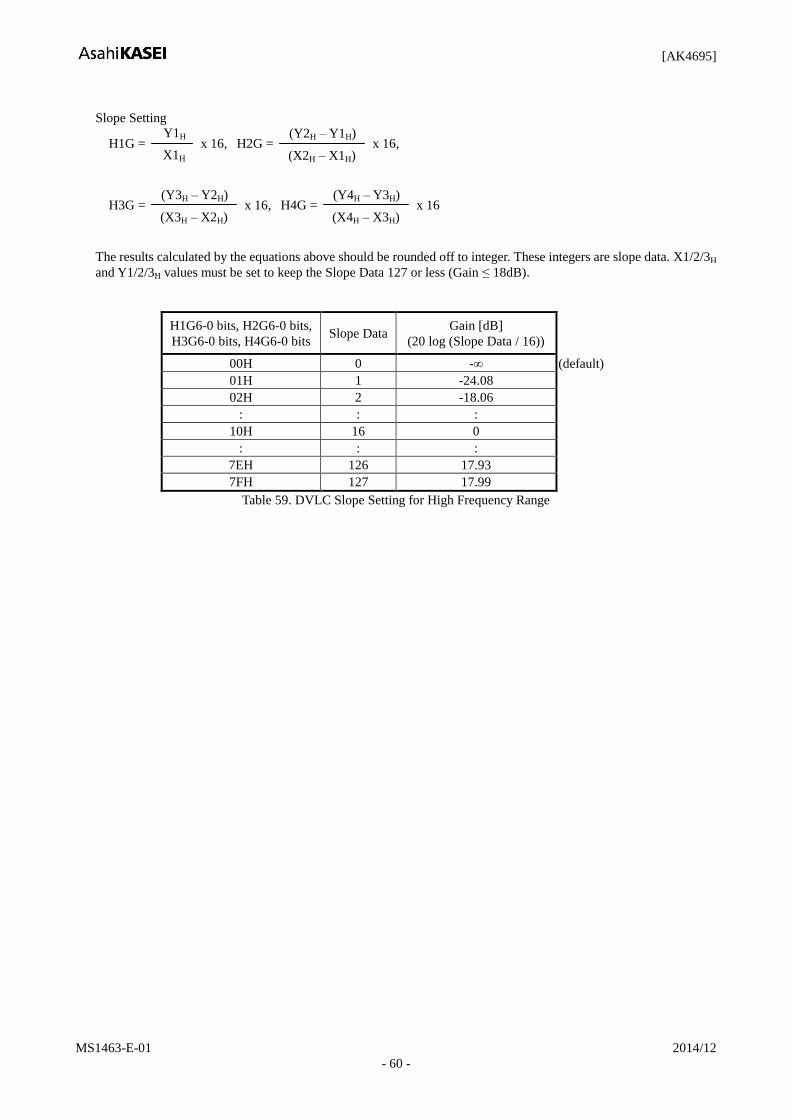
[AK4695]
MS1463-E-01 2014/12
- 60 -
Slope Setting
H1G = Y1H
X1H
x 16,
H2G = (Y2H – Y1H)
(X2H – X1H) x 16,
H3G = (Y3H – Y2H)
(X3H – X2H) x 16,
H4G = (Y4H – Y3H)
(X4H – X3H) x 16
The results calculated by the equations above should be rounded off to integer. These integers are slope data. X1/2/3H
and Y1/2/3H values must be set to keep the Slope Data 127 or less (Gain ≤ 18dB).
H1G6-0 bits, H2G6-0 bits,
H3G6-0 bits, H4G6-0 bits Slope Data
Gain [dB]
(20 log (Slope Data / 16))
00H 0 -∞ (default)
01H 1 -24.08
02H 2 -18.06
: : :
10H 16 0
: : :
7EH 126 17.93
7FH 127 17.99
Table 59. DVLC Slope Setting for High Frequency Range

[AK4695]
MS1463-E-01 2014/12
- 61 -
(4) Dynamic Volume Control
The DVLC automatically controls the volume at the attenuation speed set by DVLMAT2-0 bits (Table 61) or the recovery
speed set by DVRGAIN2-0 bits (Table 62) in such a way that the input moving average level set by DAF1-0 bits (Table 60)
is reached the output level of the DVLC curve set by each frequency range.
DAF1-0 bits Moving Average Parameter
fs=8kHz fs=16kHz fs=48kHz
00 256/fs 32ms 16ms 5.3ms
01 512/fs 64ms 32ms 10.7ms
10 1024/fs 128ms 64ms 21.3ms
11 2048/fs 256ms 128ms 42.7ms (default)
Table 60. DVLC Moving Average Parameter Setting
DVLMAT2 DVLMAT1 DVLMAT0 ATT Speed bit bit bit 8kHz 16kHz 48kHz
0 0 0 1.1dB/s 2.1dB/s 6.4dB/s
0 0 1 2.1dB/s 4.2dB/s 12.7dB/s
0 1 0 4.2dB/s 8.5dB/s 25.4dB/s
0 1 1 8.5dB/s 17.0dB/s 50.9dB/s (default)
1 0 0 17.0dB/s 33.9dB/s 101.8dB/s
1 0 1 33.9dB/s 67.9dB/s 203.6dB/s
1 1 0 67.9dB/s 135.8dB/s 407.4dB/s
1 1 1 N/A
Table 61. DVLC ATT Speed Setting (N/A: Not Available)
DVRGAIN2 bit
DVRGAIN1 bit
DVRGAIN0 bit
Recovery Speed
8kHz 16kHz 48kHz
0 0 0 0.07dB/s 0.13dB/s 0.40dB/s
0 0 1 0.13dB/s 0.27dB/s 0.80dB/s
0 1 0 0.27dB/s 0.53dB/s 1.60dB/s
0 1 1 0.53dB/s 1.06dB/s 3.18dB/s (default)
1 0 0 1.06dB/s 2.12dB/s 6.36dB/s
1 0 1 2.12dB/s 4.24dB/s 12.7dB/s
1 1 0 4.24dB/s 8.48dB/s 25.4dB/s
1 1 1 N/A
Table 62. DVLC Recovery Speed Setting (N/A: Not Available)

[AK4695]
MS1463-E-01 2014/12
- 62 -
3. Dynamic Range Control Block
The AK4695 has the dynamic range control (DRC) circuits. The compression level is selected in three levels and set by
DRCC1-0 bits (Table 63).
When the DRC is OFF (DRCC1-0 bits = “00”), the audio data passes this block by 0dB gain. However limiter and recovery
operation is always ON. The compression level must be set when PMDRC bit = “0”.
0dB
DRC Input Level (dB)
DR
C O
utp
ut L
eve
l (d
B)
0dB DRC Off
Mid Low
High
-6dB
-6dB
+3.5dB +1.0dB
+1.9dB
Figure 40. DRC Gain Curve
DRCC1 bit DRCC0 bit Compression Level
0 0 OFF (default)
0 1 Low
1 0 Middle
1 1 High
Table 63. DRC Compression Level Select
1. DRC Limiter Operation
During the DRC limiter operation, when the output level of DRC exceeds full-scale, the DRC volume are attenuated
automatically with the soft transition in the attenuation speed set by DLMAT2-0 bits (Table 64).
DLMAT2 bit
DLMAT1 bit
DLMAT0 bit
ATT Speed 8kHz 16kHz 48kHz
0 0 0 0.1dB/ms 0.3dB/ms 0.8dB/ms (default)
0 0 1 0.3dB/ms 0.5dB/ms 1.6dB/ms
0 1 0 0.5dB/ms 1.1dB/ms 3.3dB/ms
0 1 1 1.1dB/ms 2.2dB/ms 6.6dB/ms
1 0 0 2.2dB/ms 4.4dB/ms 13.2dB/ms
1 0 1 4.5dB/ms 9.0dB/ms 26.9dB/ms
1 1 0 N/A
1 1 1
Table 64. DRC ATT Speed Setting (N/A: Not Available)
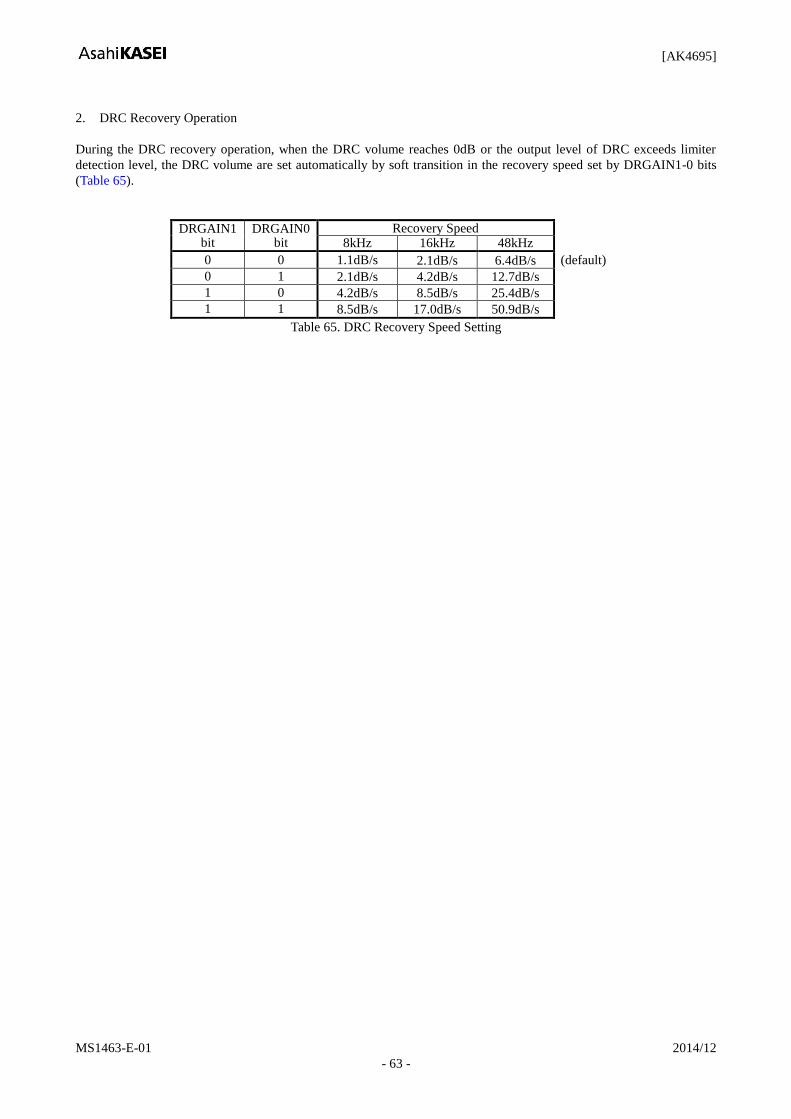
[AK4695]
MS1463-E-01 2014/12
- 63 -
2. DRC Recovery Operation
During the DRC recovery operation, when the DRC volume reaches 0dB or the output level of DRC exceeds limiter
detection level, the DRC volume are set automatically by soft transition in the recovery speed set by DRGAIN1-0 bits
(Table 65).
DRGAIN1 bit
DRGAIN0 bit
Recovery Speed 8kHz 16kHz 48kHz
0 0 1.1dB/s 2.1dB/s 6.4dB/s (default)
0 1 2.1dB/s 4.2dB/s 12.7dB/s
1 0 4.2dB/s 8.5dB/s 25.4dB/s
1 1 8.5dB/s 17.0dB/s 50.9dB/s
Table 65. DRC Recovery Speed Setting

[AK4695]
MS1463-E-01 2014/12
- 64 -
Digital Output Volume A and B
The AK4695 has a digital output volume (256 levels including Mute, 0.5dB step). The volume can be set by the DVLA7-0
and DVLB7-0 bits. The volume is included in front of the DACA (DACB) block. The input data of DAC is changed from
+12dB to –115dB or MUTE. Both Lch and Rch attenuation levels are controlled together by DVLA7-0 bits or DVLB7-0
bits. This volume has soft transition function. Therefore no switching noise occurs during the transition. The DVTMA
(DVTMB) bit sets the transition time between set values of DVLA7-0 (DVLB7-0) bits (from 00H to FFH) as either 256/fs
or 512/fs (Table 67). When DVTMA (DVTMB) bit = “1”, it takes 512/fs (10.7ms@fs=48kHz) from 00H (MUTE) to FFH
(+12dB).
DVLA7-0 bits
DVLB7-0 bits Gain Step
FFH +12.0dB
0.5dB
FEH +11.5dB
FDH +11.0dB
: :
E7H 0dB (default)
:
02H 114.5dB
01H 115.0dB
00H Mute ( )
Table 66. Digital Output Volume A and B Setting
DVTMA bit
DVTMB bit
Transition Time between DVLA7-0 bits = 00H and FFH
Transition Time between DVLB7-0 bits = 00H and FFH
Setting fs=8kHz fs=48kHz
0 256/fs 32ms 5.3ms
1 512/fs 64ms 10.7ms (default)
Table 67. Transition Time Setting of Digital Output Volume A and B

[AK4695]
MS1463-E-01 2014/12
- 65 -
Soft Mute A and B
Soft mute operation is performed in the digital domain. When the SMUTEA (SMUTEB) bit is set “1”, the output signal is
attenuated by -∞ (“0”) during the cycle set by DVTMA (DVTMB) bit. When the SMUTEA (SMUTEB) bit is returned to
“0”, the mute is cancelled and the output attenuation level gradually changes to the value set by DVLA7-0 (DVLB7-0) bits
from -∞ during the cycle set by DVTMA (DVTMB) bit. If the soft mute is cancelled within the cycle set by DVTMA
(DVTMB) bit after starting the operation, the attenuation is discontinued and returned to the level set by DVLA7-0
(DVLB7-0) bits. The soft mute is effective for changing the signal source without stopping the signal transaction (Figure
41)
SMUTEA bit SMUTEB bit
Attenuation
DVLA7-0 bits DVLB7-0 bits
- GD GD
(1)
(2)
(3)
Analog Output
(1)
DVTMA bit DVTMB bit
DVTMA bit DVTMB bit
Figure 41. Soft Mute A/B Function
(1) The input signal is attenuated by (“0”) during the cycle set by DVTMA (DVTMB) bit.
(2) Analog output corresponding to digital input has group delay (GD).
(3) If soft mute is cancelled within the cycle set by DVTMA (DVTMB) bit after starting the operation, the attenuation is
discounted and returned to the value set by DVLA7-0 (DVLB7-0) bits within the same cycle.
General Output Port (GPO1 pin)
The GPO1 pin of the AK4695 can be used as a general output pin. GPO11 and GPO10 bits select the output data of the
GPO1 pin. The GPO1 pin outputs Hi-Z at default setting and in power-down status.
GPO11 bit GPO10 bit GPO1 pin
0 0 Hi-Z (default)
0 1 “L” output
1 0 “H” output
1 1 N/A
Table 68. GPO1 Register Setting (N/A: Not available)

[AK4695]
MS1463-E-01 2014/12
- 66 -
Beep Input
When BEEPS bit is set to “1” during PMBP bit= “1”, the input signal from the BEEPIN pin is output to Speaker-Amp or
Line-Amp B. BPGN2-0 bits set the BEEP gain (Table 69) and the total gain is determined according to SPKG1-0 bits
setting (Table 76). When PMVCM bit = “1” and PMBP bit = “0”, the AK4695 is in power-save mode and the BEEPPIN
pin output becomes VCOM voltage. In this case, the input impedance is 50kΩ (typ). The rise-up time to the 99% VCOM
voltage is typ. 25ms@+2dB ~ 36ms@+16dB when input capacitance is 0.1μF.
BPGN2 bit BPGN1 bit BPGN0 bit BEEP Gain
0 0 0 2dB (default)
0 0 1 4dB
0 1 0 6dB
0 1 1 8dB
1 0 0 10dB
1 0 1 12dB
1 1 0 14dB
1 1 1 16dB
Table 69. BEEP Output Gain Setting
SPKG1-0
bits
SPK-Amp Output (BTL)
Total Gain
(BEEP Gain = 2dB)
Output Level
(BEEPIN Inptu=1.34Vpp,
AVDD=SVDD=2.8V)
00 7.6dB 3.21Vpp (default)
01 9.6dB 4.05Vpp (Note 50)
10 11.6dB 5.09Vpp (Note 50)
11 16.6dB 9.06Vpp (Note 50)
Note 50. The output level is calculated on the assumption that the signal is not clipped. However, in the actual case, the
SPK-Amp output is clipped when a 1.34Vpp signal is input to the BEEPIN pin. The input signal level of the
BEEPIN pin should be lowered to avoid this clipping.
Table 70. BEEPIN pin → SPP/SPN pins Gain
BEEPIN pin
SPP/SPN pin (LOUTB/ROUTB pin)
BEEPS bit
Beep-Amp
50kΩ(typ)
VCOM
50kΩ(typ)
Power-save Mode
0.1μF
PMBP bit
Figure 42. Block Diagram of BEEPIN pin
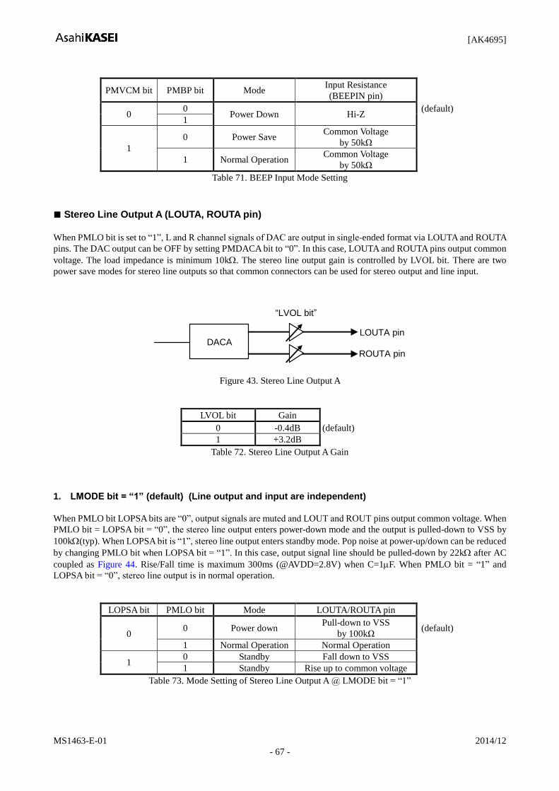
[AK4695]
MS1463-E-01 2014/12
- 67 -
PMVCM bit PMBP bit Mode Input Resistance
(BEEPIN pin)
0 0
Power Down Hi-Z (default)
1
1
0 Power Save Common Voltage
by 50kΩ
1 Normal Operation Common Voltage
by 50kΩ
Table 71. BEEP Input Mode Setting
Stereo Line Output A (LOUTA, ROUTA pin)
When PMLO bit is set to “1”, L and R channel signals of DAC are output in single-ended format via LOUTA and ROUTA
pins. The DAC output can be OFF by setting PMDACA bit to “0”. In this case, LOUTA and ROUTA pins output common
voltage. The load impedance is minimum 10k. The stereo line output gain is controlled by LVOL bit. There are two
power save modes for stereo line outputs so that common connectors can be used for stereo output and line input.
DACA LOUTA pin
ROUTA pin
“LVOL bit”
Figure 43. Stereo Line Output A
LVOL bit Gain
0 -0.4dB (default)
1 +3.2dB
Table 72. Stereo Line Output A Gain
1. LMODE bit = “1” (default) (Line output and input are independent)
When PMLO bit LOPSA bits are “0”, output signals are muted and LOUT and ROUT pins output common voltage. When
PMLO bit = LOPSA bit = “0”, the stereo line output enters power-down mode and the output is pulled-down to VSS by
100k(typ). When LOPSA bit is “1”, stereo line output enters standby mode. Pop noise at power-up/down can be reduced
by changing PMLO bit when LOPSA bit = “1”. In this case, output signal line should be pulled-down by 22k after AC
coupled as Figure 44. Rise/Fall time is maximum 300ms (@AVDD=2.8V) when C=1F. When PMLO bit = “1” and
LOPSA bit = “0”, stereo line output is in normal operation.
LOPSA bit PMLO bit Mode LOUTA/ROUTA pin
0 0 Power down
Pull-down to VSS
by 100kΩ (default)
1 Normal Operation Normal Operation
1 0 Standby Fall down to VSS
1 Standby Rise up to common voltage
Table 73. Mode Setting of Stereo Line Output A @ LMODE bit = “1”

[AK4695]
MS1463-E-01 2014/12
- 68 -
LOUTA pin ROUTA pin
1F
1k
22k
DACA
Figure 44. External Circuit of Stereo Line Output A (in case of using a Pop Noise Reduction Circuit)
[Stereo Line Output A Control Sequence (in case of using a Pop Noise Reduction Circuit)]
PMLO bit
LOPSA bit
LOUTA, ROUTA pins
(1)
(2)
Normal Output
(3) (4)
(5)
(6)
max.?300 ms max. 300 ms
99% Common Voltage
1% Common Voltage
Figure 45. Stereo Line Output A Control Sequence (in case of using a Pop Noise Reduction Circuit)
(1) Set LOPSA bit = “1”. Stereo line output enters standby mode.
(2) Set PMLO bit = “1”. Stereo line output exits power-down mode.
LOUTA and ROUTA pins rise up to common voltage. Rise time is 200ms (max 300ms) when C=1F.
(3) Set LOPSA bit = “0” after LOUTA and ROUTA pins rise up. Stereo line output exits standby mode.
Stereo line output is enabled.
(4) Set LOPSA bit = “1”. Stereo line output enters standby mode.
(5) Set PMLO bit = “0”. Stereo line output enters power-down mode.
LOUTA and ROUTA pins fall down to 1% of the common voltage. Fall time is 200ms (max 300ms) at C=1F.
(6) Set LOPSA bit = “0” after LOUTA and ROUTA pins fall down. Stereo line output exits standby mode.
2. LMODE bit = “0” (using a same connector for both Line input and output)
When PMLO bit is “0”, LOUTA and ROUTA pins are in power-down mode and output Hi-Z signal.
When PMLO bit is “1”, the LOUTA/ROUTA pin enters power-save mode and the output is pulled-down to common
voltage via an internal resistor of 200k(typ). In this case, the signal path of the stereo line output (DACA) is OFF. Pop
noise can be reduced by using power save mode by LMODE bit = “1”. Line input should be made in power-save mode.
PMLO bit LOPSA bit Mode LOUTA/ROUTA pin
0 x Power Down Hi-Z (default)
1 x Power Save Common Voltage
by 200k
Table 74. Stereo Line Output Mode Setting @ LMODE bit = “0” (x: Don’t care)

[AK4695]
MS1463-E-01 2014/12
- 69 -
AUXINL pin (AUXINR pin)
typ.100k
To ADC
MIC-Amp
typ.200k
VCOM
VCOM
LOUTA pin (ROUTA pin)
Connector (Line Input)
Power-save Mode
1k 22k
AVDD
AVDD
Figure 46. Connection Example of when using a Same Connector for Both Line Input and Output
[Line Input Mode Control Sequence (in case of not using a Pop Noise Reduction Circuit)]
PMLO bit
LOPSA bit
LOUTA pin ROUTA pin
(1)
VCOM
(3) (4)
(5)
LMODE bit
AUXINL pin AUXINR pin
Power-save
0
(2) (2)
Normal Operation
Power-down Power-down
Figure 47. Line Input Mode Control Sequence (in case of not using a Pop Noise Reduction Circuit)
(1) Set PMLO bit = “1”. Stereo line output exits power-down mode.
LOUTA and ROUTA pins rise up to common voltage.
(2) Voltage Fluctuation period.
(3) Set LMODE bit = “0” after LOUTA and ROUTA pins rise up.
Line input is enabled.
(4) Set LMODE bit = “1”. Line input mode is disabled.
(5) Set PMLO bit = “0”. Stereo line output enters power-down mode.
LOUTA and ROUTA pins fall down.

[AK4695]
MS1463-E-01 2014/12
- 70 -
Charge Pump Circuit
The internal charge pump circuit generates negative voltage (PVEE) from SVDD voltage. The PVEE voltage is used for
the headphone amplifier. The charge pump circuit starts operation when PMHPL or PMHPR bit = “1” and PMDACB bit =
“1”. PMVCM bit must be set “1” to power up the charge pump circuit. The power-up time of the charge pump circuit is
8ms (max). The headphone amplifier will be powered up after the charge pump circuit is powered up (when PMHPL or
PMHPR bit = “1”). The operating frequency of the charge pump circuit is dependent on the sampling frequency.
Headphone Amplifier (HPL/HPR pins)
The positive voltage of the headphone amplifier uses the power supply to the DVDD pin, therefore 200mA of the
maximum power supply capacity is needed. The internal charge pump circuit generates negative voltage (PVEE) from
SVDD voltage. The headphone amplifier output is single-ended and centered around on VSS (0V). Therefore, the
capacitor for AC-coupling can be removed. The minimum load resistance is 16. The headphone amplifier output may be
clipped when a 0dB signal is input from DACB depending on the power supply conditions. The headphone amplifier
should be used in the following condition to avoid this clipping.
SVDD ≥ AVDD, DVDD ≥ 0.54 x AVDD
<External Circuit of Headphone-Amp>
An oscillation prevention circuit (0.22μF±20% capacitor and 100Ω±20% resistor) should be put because it has the
possibility that Headphone-Amp oscillates in type of headphone.
HP-AMP
DACB
AK4695 16Ω
Headphone
0.22μ
100Ω
HPL pin HPR pin
Figure 48. External Circuit of Headphone-Amp
When PMDACB bit = “1”, HPZ bit = “0”, DACAST bit = “1” and PMHPL, PMHPR bits = “1”, headphone outputs are in
normal operation. The headphone-amps are powered-down completely by setting PMHPL and PMHPR bits = “0”. At that
time, the HPL and HPR pins go to VSS voltage via the internal pulled-down resistor. The pulled-down resistor is 10 (typ).
The HPL and HPR pins become Hi-Z state by setting HPZ bit to “1” when PMHPL and PMHPR bit = “0”. The power-up
time of the headphone-amps is 26ms (max.), and power-down is executed immediately.
PMVCM
bit PMHP bit HPZ bit Mode HPL/R pins
x 0 0 Power-down & Mute Pull-down by 10 (typ) (default)
x 0 1 Power-down Hi-Z
1 1 0 Normal Operation Normal Operation
1 1 1 N/A N/A
Table 75. Headphone Output Status (x: Don’t’ care, N/A: Not available)

[AK4695]
MS1463-E-01 2014/12
- 71 -
Thermal Shutdown Function
When the internal device temperature rises up irregularly (E.g. Output pins of speaker amplifier are shortened.), the charge
pump, headphone amplifier and speaker amplifier are automatically powered down. When the internal temperature goes
down and the thermal shutdown is released, the charge pump, speaker amplifier and headphone amplifier are powered up
automatically and the AK4695 returns to the setting before thermal shutdown. If the status registers are changed during
thermal shutdown, the AK4695 reflects the new setting when thermal shutdown is released. The thermal shutdown function
is enabled when THSDN bit = “0”, and disabled when THSDN bit = “1” (default).

[AK4695]
MS1463-E-01 2014/12
- 72 -
Speaker Output (SPP/SPN pins: LBSEL bit = “0”)
The DACB output signal is input to the speaker amplifier as [(L+R)/2] when LBSEL bit = “0” and DACS bit = “1”. The
speaker amplifier is mono and BTL output. The gain is set by SPKG1-0 bits and the output level depends on this setting. In
the condition that AVDD > SVDD, the speaker amplifier output is clipped by a 0dBFS input from DACB. The DACB
output level should be set to a lower level by setting DVLB bits to avoid this clipping.
SPKG1-0 bits SPK-Amp Gain (BTL)
00 5.6dB (default)
01 7.6dB
10 9.6dB
11 14.6dB
Table 76. SPK-Amp Gain
SPKG1-0 bits SPK-Amp Output (Note 51)
(DAC Input =0dBFS, AVDD=SVDD=2.8V)
00 3.91Vpp
01 4.92Vpp
10 6.20Vpp
11 11.02Vpp
Note 51. The output level is calculated by assuming that output signal is not clipped. In the actual case, the output signal
may be clipped when DACB outputs a 0dBFS signal. The DACB output level should be set to a lower level by
setting digital volume (DVLB bits) so that the speaker amplifier output is not clipped.
Table 77. SPK-Amp Output Level
< Speaker-Amp Control Sequence >
The speaker amplifier is powered-up/down by PMSPLO bit. When PMSPLO bit is “0”, both SPP and SPN pins are in a
Hi-Z state. When PMSPK bit is “1” and SPPSN bit is “0”, the speaker amplifier enters power-save mode. In this mode, the
SPP pin is placed in a Hi-Z state and the SPN pin outputs SVDD/2 voltage.
When the PMSPLO bit is “1”, writing “1” to LBSEL bit is ignored. The SPP and SPN pins rise up in power-save mode
setting PMSPLO bit to “0” after the PDN pin is changed from “L” to “H”. In this mode, the SPP pin is placed in a Hi-Z state
and the SPN pin goes to SVDD/2 voltage. Because the SPP and SPN pins rise up in power-save mode, pop noises are
reduced. When the AK4695 is powered-down, a pop noise can also be reduced by first entering power-save mode.
PMSPLO bit SPPSN bit Mode SPP pin SPN pin
0 x Power-down Hi-Z Hi-Z (default)
1 0 Power-save Hi-Z SVDD/2
1 Normal Operation Normal Operation Normal Operation
Table 78 Speaker-Amp Mode Setting (x: Don’t care)
PMSPLO bit
SPPSN bit
SPP pin
SPN pin SVDD/2 SVDD/2
Hi-Z Hi-Z
Hi-Z Hi-Z
>1ms
Figure 49. Power-up/Power-down Timing for Speaker-Amp
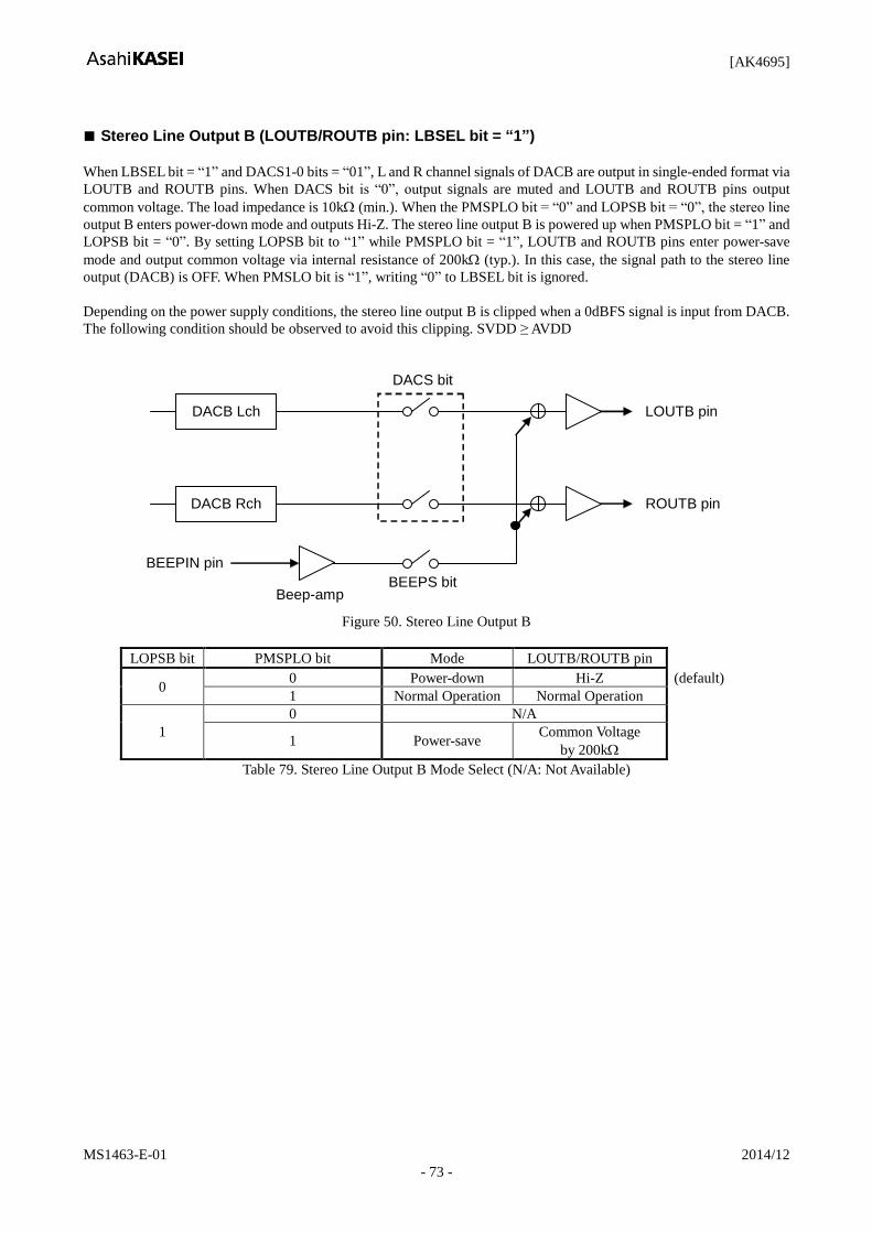
[AK4695]
MS1463-E-01 2014/12
- 73 -
Stereo Line Output B (LOUTB/ROUTB pin: LBSEL bit = “1”)
When LBSEL bit = “1” and DACS1-0 bits = “01”, L and R channel signals of DACB are output in single-ended format via
LOUTB and ROUTB pins. When DACS bit is “0”, output signals are muted and LOUTB and ROUTB pins output
common voltage. The load impedance is 10k (min.). When the PMSPLO bit = “0” and LOPSB bit = “0”, the stereo line
output B enters power-down mode and outputs Hi-Z. The stereo line output B is powered up when PMSPLO bit = “1” and
LOPSB bit = “0”. By setting LOPSB bit to “1” while PMSPLO bit = “1”, LOUTB and ROUTB pins enter power-save
mode and output common voltage via internal resistance of 200k (typ.). In this case, the signal path to the stereo line
output (DACB) is OFF. When PMSLO bit is “1”, writing “0” to LBSEL bit is ignored.
Depending on the power supply conditions, the stereo line output B is clipped when a 0dBFS signal is input from DACB.
The following condition should be observed to avoid this clipping. SVDD ≥ AVDD
DACS bit
LOUTB pin
ROUTB pin DACB Rch
DACB Lch
BEEPIN pin
Beep-amp BEEPS bit
Figure 50. Stereo Line Output B
LOPSB bit PMSPLO bit Mode LOUTB/ROUTB pin
0 0 Power-down Hi-Z (default)
1 Normal Operation Normal Operation
1
0 N/A
1 Power-save Common Voltage
by 200k
Table 79. Stereo Line Output B Mode Select (N/A: Not Available)

[AK4695]
MS1463-E-01 2014/12
- 74 -
LOUTB pin ROUTB pin
C
RL
DACB External Input
Figure 51. External Circuit for Stereo Line Output B
[Stereo Line Output B Control Sequence (in case of using external MUTE circuit)]
PMSPLO bit
External Input
(1) (9)
GPO11, 10 bits (External MUTE)
(2)
(5) (6)
LOUTB pin ROUTB pin
Normal Operation MUTE MUTE
Power Save
Power Save
(3) (4) (7) (8)
LOPSB bit
Hi-Z
Figure 52. Stereo Line Output B Control Sequence (in case of using external MUTE circuit)
(1) Set PMSPLO bit = “1”. Stereo line output B exits power-down mode.
LOUT and ROUT pins rise up to common voltage.
(2) Time constant is defined according to external capacitor (C) and resistor (RL).
(3) Set LOPSB bit = “1”. Stereo line output B enters power-save mode.
In this mode, the power consumption is reduced.
(4) Set LOPSB bit = “0”. Stereo line output B exits power-save mode.
(5) Release external MUTE when the external input is stabled. GPO11, 10 bits = “10” (“H” output).
Stereo line output is enabled.
(6) Set external MUTE ON. GPO11, 10 bits = “01” (“L” output)
(7) Set LOPSB bit = “1”. Stereo line output B enters power-save mode.
In this mode, the power consumption is reduced.
(8) Set LOPSB bit = “0”. Stereo line output B exits power-save mode.
(9) Set PMSPLO bit = “0”. Stereo line output B enters power-down mode.
LOUTB and ROUTB pins are in Hi-Z state.
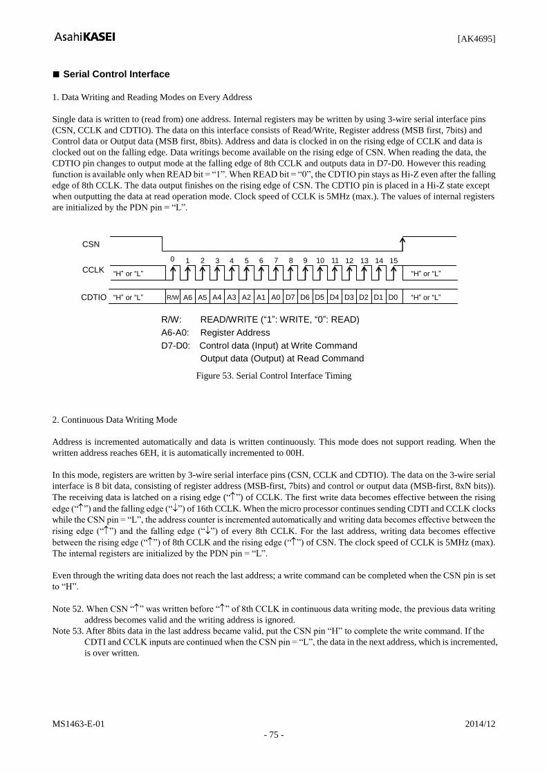
[AK4695]
MS1463-E-01 2014/12
- 75 -
Serial Control Interface
1. Data Writing and Reading Modes on Every Address
Single data is written to (read from) one address. Internal registers may be written by using 3-wire serial interface pins
(CSN, CCLK and CDTIO). The data on this interface consists of Read/Write, Register address (MSB first, 7bits) and
Control data or Output data (MSB first, 8bits). Address and data is clocked in on the rising edge of CCLK and data is
clocked out on the falling edge. Data writings become available on the rising edge of CSN. When reading the data, the
CDTIO pin changes to output mode at the falling edge of 8th CCLK and outputs data in D7-D0. However this reading
function is available only when READ bit = “1”. When READ bit = “0”, the CDTIO pin stays as Hi-Z even after the falling
edge of 8th CCLK. The data output finishes on the rising edge of CSN. The CDTIO pin is placed in a Hi-Z state except
when outputting the data at read operation mode. Clock speed of CCLK is 5MHz (max.). The values of internal registers
are initialized by the PDN pin = “L”.
CSN
CCLK
0 1 2 3 4 5 6 7 8 9 10 11 12 13 14 15
CDTIO A6 A5 A2 A3 A1 A0 A4 D7 D6 D5 D4 D3 D2 D1 D0 R/W
R/W: READ/WRITE (“1”: WRITE, “0”: READ)
A6-A0: Register Address
D7-D0: Control data (Input) at Write Command
Output data (Output) at Read Command
“H” or “L” “H” or “L”
“H” or “L” “H” or “L”
Figure 53. Serial Control Interface Timing
2. Continuous Data Writing Mode
Address is incremented automatically and data is written continuously. This mode does not support reading. When the
written address reaches 6EH, it is automatically incremented to 00H.
In this mode, registers are written by 3-wire serial interface pins (CSN, CCLK and CDTIO). The data on the 3-wire serial
interface is 8 bit data, consisting of register address (MSB-first, 7bits) and control or output data (MSB-first, 8xN bits)).
The receiving data is latched on a rising edge (“”) of CCLK. The first write data becomes effective between the rising
edge (“”) and the falling edge (“”) of 16th CCLK. When the micro processor continues sending CDTI and CCLK clocks
while the CSN pin = “L”, the address counter is incremented automatically and writing data becomes effective between the
rising edge (“”) and the falling edge (“”) of every 8th CCLK. For the last address, writing data becomes effective
between the rising edge (“”) of 8th CCLK and the rising edge (“”) of CSN. The clock speed of CCLK is 5MHz (max).
The internal registers are initialized by the PDN pin = “L”.
Even through the writing data does not reach the last address; a write command can be completed when the CSN pin is set
to “H”.
Note 52. When CSN “” was written before “” of 8th CCLK in continuous data writing mode, the previous data writing
address becomes valid and the writing address is ignored.
Note 53. After 8bits data in the last address became valid, put the CSN pin “H” to complete the write command. If the
CDTI and CCLK inputs are continued when the CSN pin = “L”, the data in the next address, which is incremented,
is over written.
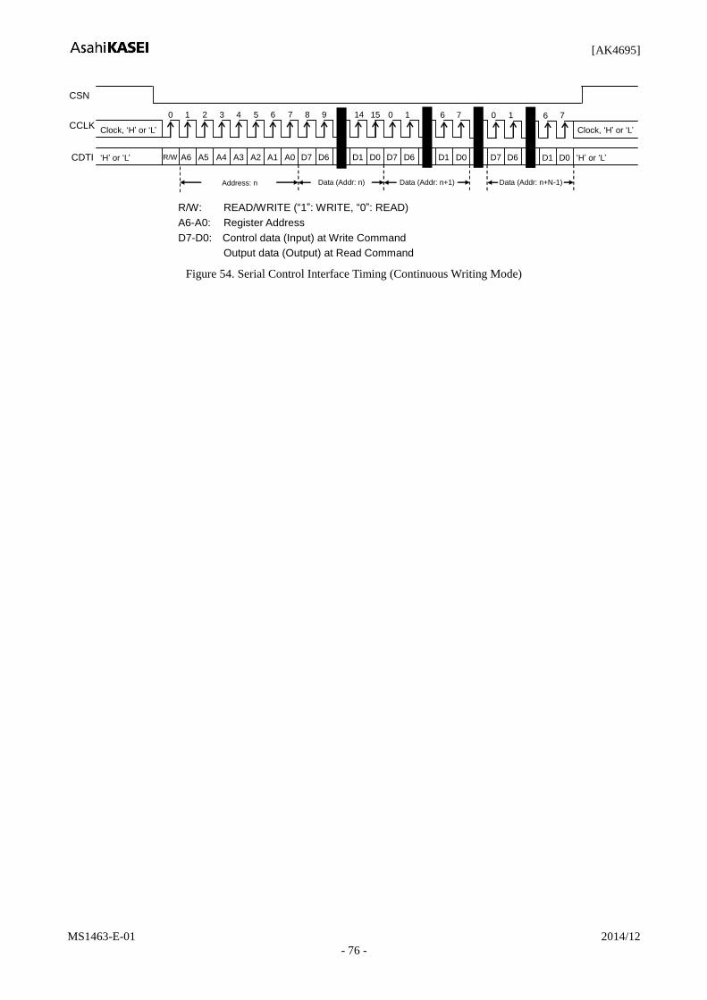
[AK4695]
MS1463-E-01 2014/12
- 76 -
CSN
CCLK 0 1 2 3 4 5 6 7 8 9 14 15 0 1
CDTI R/W A6 A2 A3 A1 A0 A4 D7 D6 D1 D0 D7 D6 A5
6
D1 D0
7 0 1
D7 D6
6
D1
7
D0
Clock, ‘H’ or ‘L’
‘H’ or ‘L’
Clock, ‘H’ or ‘L’
‘H’ or ‘L’
Address: n Data (Addr: n) Data (Addr: n+1) Data (Addr: n+N-1)
R/W: READ/WRITE (“1”: WRITE, “0”: READ)
A6-A0: Register Address
D7-D0: Control data (Input) at Write Command
Output data (Output) at Read Command
Figure 54. Serial Control Interface Timing (Continuous Writing Mode)
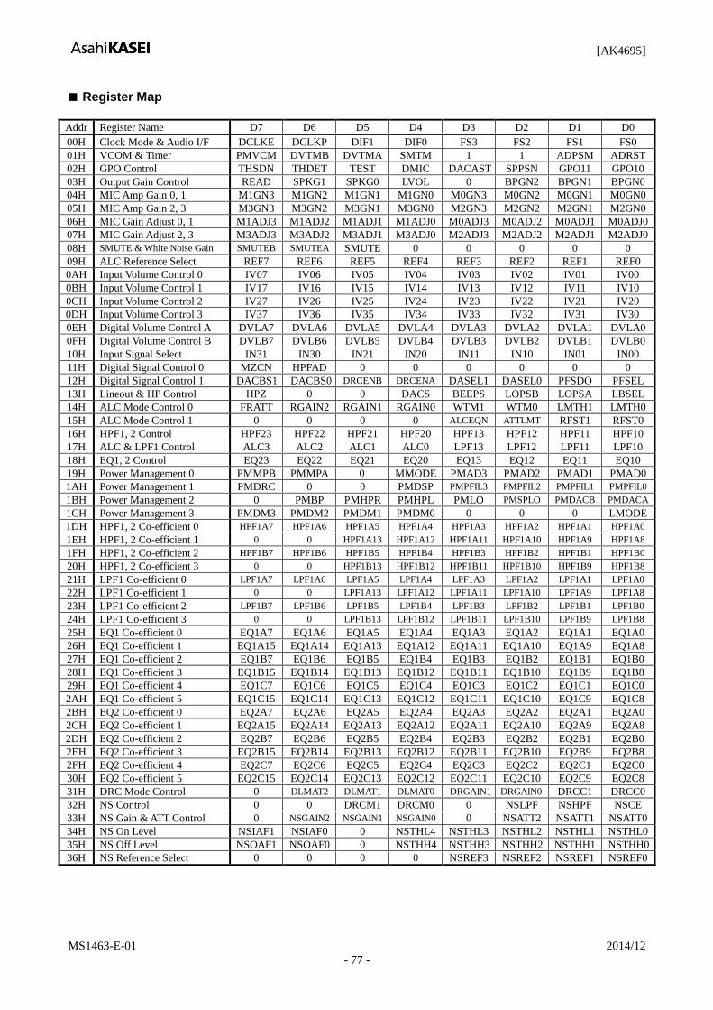
[AK4695]
MS1463-E-01 2014/12
- 77 -
Register Map
Addr Register Name D7 D6 D5 D4 D3 D2 D1 D0
00H Clock Mode & Audio I/F DCLKE DCLKP DIF1 DIF0 FS3 FS2 FS1 FS0
01H VCOM & Timer PMVCM DVTMB DVTMA SMTM 1 1 ADPSM ADRST
02H GPO Control THSDN THDET TEST DMIC DACAST SPPSN GPO11 GPO10
03H Output Gain Control READ SPKG1 SPKG0 LVOL 0 BPGN2 BPGN1 BPGN0
04H MIC Amp Gain 0, 1 M1GN3 M1GN2 M1GN1 M1GN0 M0GN3 M0GN2 M0GN1 M0GN0
05H MIC Amp Gain 2, 3 M3GN3 M3GN2 M3GN1 M3GN0 M2GN3 M2GN2 M2GN1 M2GN0
06H MIC Gain Adjust 0, 1 M1ADJ3 M1ADJ2 M1ADJ1 M1ADJ0 M0ADJ3 M0ADJ2 M0ADJ1 M0ADJ0
07H MIC Gain Adjust 2, 3 M3ADJ3 M3ADJ2 M3ADJ1 M3ADJ0 M2ADJ3 M2ADJ2 M2ADJ1 M2ADJ0
08H SMUTE & White Noise Gain SMUTEB SMUTEA SMUTE 0 0 0 0 0
09H ALC Reference Select REF7 REF6 REF5 REF4 REF3 REF2 REF1 REF0
0AH Input Volume Control 0 IV07 IV06 IV05 IV04 IV03 IV02 IV01 IV00
0BH Input Volume Control 1 IV17 IV16 IV15 IV14 IV13 IV12 IV11 IV10
0CH Input Volume Control 2 IV27 IV26 IV25 IV24 IV23 IV22 IV21 IV20
0DH Input Volume Control 3 IV37 IV36 IV35 IV34 IV33 IV32 IV31 IV30
0EH Digital Volume Control A DVLA7 DVLA6 DVLA5 DVLA4 DVLA3 DVLA2 DVLA1 DVLA0
0FH Digital Volume Control B DVLB7 DVLB6 DVLB5 DVLB4 DVLB3 DVLB2 DVLB1 DVLB0
10H Input Signal Select IN31 IN30 IN21 IN20 IN11 IN10 IN01 IN00
11H Digital Signal Control 0 MZCN HPFAD 0 0 0 0 0 0
12H Digital Signal Control 1 DACBS1 DACBS0 DRCENB DRCENA DASEL1 DASEL0 PFSDO PFSEL
13H Lineout & HP Control HPZ 0 0 DACS BEEPS LOPSB LOPSA LBSEL
14H ALC Mode Control 0 FRATT RGAIN2 RGAIN1 RGAIN0 WTM1 WTM0 LMTH1 LMTH0
15H ALC Mode Control 1 0 0 0 0 ALCEQN ATTLMT RFST1 RFST0
16H HPF1, 2 Control HPF23 HPF22 HPF21 HPF20 HPF13 HPF12 HPF11 HPF10
17H ALC & LPF1 Control ALC3 ALC2 ALC1 ALC0 LPF13 LPF12 LPF11 LPF10
18H EQ1, 2 Control EQ23 EQ22 EQ21 EQ20 EQ13 EQ12 EQ11 EQ10
19H Power Management 0 PMMPB PMMPA 0 MMODE PMAD3 PMAD2 PMAD1 PMAD0
1AH Power Management 1 PMDRC 0 0 PMDSP PMPFIL3 PMPFIL2 PMPFIL1 PMPFIL0
1BH Power Management 2 0 PMBP PMHPR PMHPL PMLO PMSPLO PMDACB PMDACA
1CH Power Management 3 PMDM3 PMDM2 PMDM1 PMDM0 0 0 0 LMODE
1DH HPF1, 2 Co-efficient 0 HPF1A7 HPF1A6 HPF1A5 HPF1A4 HPF1A3 HPF1A2 HPF1A1 HPF1A0
1EH HPF1, 2 Co-efficient 1 0 0 HPF1A13 HPF1A12 HPF1A11 HPF1A10 HPF1A9 HPF1A8
1FH HPF1, 2 Co-efficient 2 HPF1B7 HPF1B6 HPF1B5 HPF1B4 HPF1B3 HPF1B2 HPF1B1 HPF1B0
20H HPF1, 2 Co-efficient 3 0 0 HPF1B13 HPF1B12 HPF1B11 HPF1B10 HPF1B9 HPF1B8
21H LPF1 Co-efficient 0 LPF1A7 LPF1A6 LPF1A5 LPF1A4 LPF1A3 LPF1A2 LPF1A1 LPF1A0
22H LPF1 Co-efficient 1 0 0 LPF1A13 LPF1A12 LPF1A11 LPF1A10 LPF1A9 LPF1A8
23H LPF1 Co-efficient 2 LPF1B7 LPF1B6 LPF1B5 LPF1B4 LPF1B3 LPF1B2 LPF1B1 LPF1B0
24H LPF1 Co-efficient 3 0 0 LPF1B13 LPF1B12 LPF1B11 LPF1B10 LPF1B9 LPF1B8
25H EQ1 Co-efficient 0 EQ1A7 EQ1A6 EQ1A5 EQ1A4 EQ1A3 EQ1A2 EQ1A1 EQ1A0
26H EQ1 Co-efficient 1 EQ1A15 EQ1A14 EQ1A13 EQ1A12 EQ1A11 EQ1A10 EQ1A9 EQ1A8
27H EQ1 Co-efficient 2 EQ1B7 EQ1B6 EQ1B5 EQ1B4 EQ1B3 EQ1B2 EQ1B1 EQ1B0
28H EQ1 Co-efficient 3 EQ1B15 EQ1B14 EQ1B13 EQ1B12 EQ1B11 EQ1B10 EQ1B9 EQ1B8
29H EQ1 Co-efficient 4 EQ1C7 EQ1C6 EQ1C5 EQ1C4 EQ1C3 EQ1C2 EQ1C1 EQ1C0
2AH EQ1 Co-efficient 5 EQ1C15 EQ1C14 EQ1C13 EQ1C12 EQ1C11 EQ1C10 EQ1C9 EQ1C8
2BH EQ2 Co-efficient 0 EQ2A7 EQ2A6 EQ2A5 EQ2A4 EQ2A3 EQ2A2 EQ2A1 EQ2A0
2CH EQ2 Co-efficient 1 EQ2A15 EQ2A14 EQ2A13 EQ2A12 EQ2A11 EQ2A10 EQ2A9 EQ2A8
2DH EQ2 Co-efficient 2 EQ2B7 EQ2B6 EQ2B5 EQ2B4 EQ2B3 EQ2B2 EQ2B1 EQ2B0
2EH EQ2 Co-efficient 3 EQ2B15 EQ2B14 EQ2B13 EQ2B12 EQ2B11 EQ2B10 EQ2B9 EQ2B8
2FH EQ2 Co-efficient 4 EQ2C7 EQ2C6 EQ2C5 EQ2C4 EQ2C3 EQ2C2 EQ2C1 EQ2C0
30H EQ2 Co-efficient 5 EQ2C15 EQ2C14 EQ2C13 EQ2C12 EQ2C11 EQ2C10 EQ2C9 EQ2C8
31H DRC Mode Control 0 DLMAT2 DLMAT1 DLMAT0 DRGAIN1 DRGAIN0 DRCC1 DRCC0
32H NS Control 0 0 DRCM1 DRCM0 0 NSLPF NSHPF NSCE
33H NS Gain & ATT Control 0 NSGAIN2 NSGAIN1 NSGAIN0 0 NSATT2 NSATT1 NSATT0
34H NS On Level NSIAF1 NSIAF0 0 NSTHL4 NSTHL3 NSTHL2 NSTHL1 NSTHL0
35H NS Off Level NSOAF1 NSOAF0 0 NSTHH4 NSTHH3 NSTHH2 NSTHH1 NSTHH0
36H NS Reference Select 0 0 0 0 NSREF3 NSREF2 NSREF1 NSREF0

[AK4695]
MS1463-E-01 2014/12
- 78 -
Addr Register Name D7 D6 D5 D4 D3 D2 D1 D0
37H NS LPF Co-efficient 0 NSLA7 NSLA6 NSLA5 NSLA4 NSLA3 NSLA2 NSLA1 NSLA0
38H NS LPF Co-efficient 1 0 0 NSLA13 NSLA12 NSLA11 NSLA10 NSLA9 NSLA8
39H NS LPF Co-efficient 2 NSLB7 NSLB6 NSLB5 NSLB4 NSLB3 NSLB2 NSLB1 NSLB0
3AH NS LPF Co-efficient 3 0 0 NSLB13 NSLB12 NSLB11 NSLB10 NSLB9 NSLB8
3BH NS HPF Co-efficient 0 NSHA7 NSHA6 NSHA5 NSHA4 NSHA3 NSHA2 NSHA1 NSHA0
3CH NS HPF Co-efficient 1 0 0 NSHA13 NSHA12 NSHA11 NSHA10 NSHA9 NSHA8
3DH NS HPF Co-efficient 2 NSHB7 NSHB6 NSHB5 NSHB4 NSHB3 NSHB2 NSHB1 NSHB0
3EH NS HPF Co-efficient 3 0 0 NSHB13 NSHB12 NSHB11 NSHB10 NSHB9 NSHB8
3FH DVLC Filter Select DLLPF1 DLLPF0 DMHPF1 DMHPF0 DMLPF1 DMLPF0 DHHPF1 DHHPF0
40H DVLC Mode Control DVRGAIN2 DVRGAIN1 DVRGAIN0 DVLMAT2 DVLMAT1 DVLMAT0 DAF1 DAF0
41H DVLCL Curve X1 0 0 VL1X5 VL1X4 VL1X3 VL1X2 VL1X1 VL1X0
42H DVLCL Curve Y1 0 0 VL1Y5 VL1Y4 VL1Y3 VL1Y2 VL1Y1 VL1Y0
43H DVLCL Curve X2 0 0 VL2X5 VL2X4 VL2X3 VL2X2 VL2X1 VL2X0
44H DVLCL Curve Y2 0 0 VL2Y5 VL2Y4 VL2Y3 VL2Y2 VL2Y1 VL2Y0
45H DVLCL Curve X3 0 0 0 VL3X4 VL3X3 VL3X2 VL3X1 VL3X0
46H DVLCL Curve Y3 0 0 0 VL3Y4 VL3Y3 VL3Y2 VL3Y1 VL3Y0
47H DVLCL Slope 1 0 L1G6 L1G5 L1G4 L1G3 L1G2 L1G1 L1G0
48H DVLCL Slope 2 0 L2G6 L2G5 L2G4 L2G3 L2G2 L2G1 L2G0
49H DVLCL Slope 3 0 L3G6 L3G5 L3G4 L3G3 L3G2 L3G1 L3G0
4AH DVLCL Slope 4 0 L4G6 L4G5 L4G4 L4G3 L4G2 L4G1 L4G0
4BH DVLCM Curve X1 0 0 VM1X5 VM1X4 VM1X3 VM1X2 VM1X1 VM1X0
4CH DVLCM Curve Y1 0 0 VM1Y5 VM1Y4 VM1Y3 VM1Y2 VM1Y1 VM1Y0
4DH DVLCM Curve X2 0 0 VM2X5 VM2X4 VM2X3 VM2X2 VM2X1 VM2X0
4EH DVLCM Curve Y2 0 0 VM2Y5 VM2Y4 VM2Y3 VM2Y2 VM2Y1 VM2Y0
4FH DVLCM Curve X3 0 0 0 VM3X4 VM3X3 VM3X2 VM3X1 VM3X0
50H DVLCM Curve Y3 0 0 0 VM3Y4 VM3Y3 VM3Y2 VM3Y1 VM3Y0
51H DVLCM Slope 1 0 M1G6 M1G5 M1G4 M1G3 M1G2 M1G1 M1G0
52H DVLCM Slope 2 0 M2G6 M2G5 M2G4 M2G3 M2G2 M2G1 M2G0
53H DVLCM Slope 3 0 M3G6 M3G5 M3G4 M3G3 M3G2 M3G1 M3G0
54H DVLCM Slope 4 0 M4G6 M4G5 M4G4 M4G3 M4G2 M4G1 M4G0
55H DVLCH Curve X1 0 0 VH1X5 VH1X4 VH1X3 VH1X2 VH1X1 VH1X0
56H DVLCH Curve Y1 0 0 VH1Y5 VH1Y4 VH1Y3 VH1Y2 VH1Y1 VH1Y0
57H DVLCH Curve X2 0 0 VH2X5 VH2X4 VH2X3 VH2X2 VH2X1 VH2X0
58H DVLCH Curve Y2 0 0 VH2Y5 VH2Y4 VH2Y3 VH2Y2 VH2Y1 VH2Y0
59H DVLCH Curve X3 0 0 0 VH3X4 VH3X3 VH3X2 VH3X1 VH3X0
5AH DVLCH Curve Y3 0 0 0 VH3Y4 VH3Y3 VH3Y2 VH3Y1 VH3Y0
5BH DVLCH Slope 1 0 H1G6 H1G5 H1G4 H1G3 H1G2 H1G1 H1G0
5CH DVLCH Slope 2 0 H2G6 H2G5 H2G4 H2G3 H2G2 H2G1 H2G0
5DH DVLCH Slope 3 0 H3G6 H3G5 H3G4 H3G3 H3G2 H3G1 H3G0
5EH DVLCH Slope 4 0 H4G6 H4G5 H4G4 H4G3 H4G2 H4G1 H4G0
5FH DVLCL LPF Co-efficient 0 DLLA7 DLLA6 DLLA5 DLLA4 DLLA3 DLLA2 DLLA1 DLLA0
60H DVLCL LPF Co-efficient 1 0 0 DLLA13 DLLA12 DLLA11 DLLA10 DLLA9 DLLA8
61H DVLCL LPF Co-efficient 2 DLLB7 DLLB6 DLLB5 DLLB4 DLLB3 DLLB2 DLLB1 DLLB0
62H DVLCL LPF Co-efficient 3 0 0 DLLB13 DLLB12 DLLB11 DLLB10 DLLB9 DLLB8
63H DVLCM HPF Co-efficient 0 DMHA7 DMHA6 DMHA5 DMHA4 DMHA3 DMHA2 DMHA1 DMHA0
64H DVLCM HPF Co-efficient 1 0 0 DMHA13 DMHA12 DMHA11 DMHA10 DMHA9 DMHA8
65H DVLCM HPF Co-efficient 2 DMHB7 DMHB6 DMHB5 DMHB4 DMHB3 DMHB2 DMHB1 DMHB0
66H DVLCM HPF Co-efficient 3 0 0 DMHB13 DMHB12 DMHB11 DMHB10 DMHB9 DMHB8
67H DVLCM LPF Co-efficient 0 DMLA7 DMLA6 DMLA5 DMLA4 DMLA3 DMLA2 DMLA1 DMLA0
68H DVLCM LPF Co-efficient 1 0 0 DMLA13 DMLA12 DMLA11 DMLA10 DMLA9 DMLA8
69H DVLCM LPF Co-efficient 2 DMLB7 DMLB6 DMLB5 DMLB4 DMLB3 DMLB2 DMLB1 DMLB0
6AH DVLCM LPF Co-efficient 3 0 0 DMLB13 DMLB12 DMLB11 DMLB10 DMLB9 DMLB8
6BH DVLCH HPF Co-efficient 0 DHHA7 DHHA6 DHHA5 DHHA4 DHHA3 DHHA2 DHHA1 DHHA0
6CH DVLCH HPF Co-efficient 1 0 0 DHHA13 DHHA12 DHHA11 DHHA10 DHHA9 DHHA8
6DH DVLCH HPF Co-efficient 2 DHHB7 DHHB6 DHHB5 DHHB4 DHHB3 DHHB2 DHHB1 DHHB0
6EH DVLCH HPF Co-efficient 3 0 0 DHHB13 DHHB12 DHHB11 DHHB10 DHHB9 DHHB8
Note 54. PDN pin = “L” resets the registers to their default values.
Note 55. The bits defined as 0 must contain a “0” value.
Note 56. The bits defined as 1 must contain a “1” value.
Note 57. Writing access to 6FH ~ FFH is prohibited.

[AK4695]
MS1463-E-01 2014/12
- 79 -
Register Definitions
Addr Register Name D7 D6 D5 D4 D3 D2 D1 D0
00H Clock Mode & Audio I/F DCLKE DCLKP DIF1 DIF0 FS3 FS2 FS1 FS0
R/W R/W R/W R/W R/W R/W R/W R/W R/W
Default 0 0 1 0 0 0 1 0
FS3-0: Sampling Frequency Setting (Table 2)
Default: “0010” (256fs: 32kHz < fs ≤ 48kHz)
DIF1-0: Audio Interface Format (Table 5)
Default: “10” (24bit Left justified)
DCLKP: Data Latching Edge Select 0: Lch data is latched on the DMCLK rising edge (“”). (default)
1: Lch data is latched on the DMCLK falling edge (“”).
DCLKE: DMCLK pin Output Clock Control 0: “L” Output (default) 1: 64fs Output
Addr Register Name D7 D6 D5 D4 D3 D2 D1 D0
01H VCOM & Timer PMVCM DVTMB DVTMA SMTM 1 1 ADPSM ADRST
R/W R/W R/W R/W R/W R R R/W R/W
Default 0 1 1 1 1 1 0 0
ADRST: ADC Initial Cycle Setting
0: 1059/fs (default)
1: 267/fs
ADPSM: ADC Low Power Consumption Mode
0: Normal Operation (default)
1: Low Power Consumption Operation
SMTM: Soft Mute Transition Time Setting
0: 240/fs
1: 480/fs (default)
DVTMA: Digital Volume A Soft Transition Time Setting
0: 256/fs
1: 512/fs (default)
This is the transition time between DVLA7-0 bits = FFH and 00H.
DVTMB: Digital Volume B Soft Transition Time Setting
0: 256/fs
1: 512/fs (default)
This is the transition time between DVLB7-0 bits = FFH and 00H.
PMVCM: VCOM Power Management
0: Power down (default)
1: Power up
PMVCM bit must be “1” when one of bocks is powered-up. PMVCM bit can only be “0” when all power
management bits are “0”.

[AK4695]
MS1463-E-01 2014/12
- 80 -
Addr Register Name D7 D6 D5 D4 D3 D2 D1 D0
02H GPO Control THSDN THDET TEST DMIC DACAST SPPSN GPO11 GPO10
R/W R/W R R/W R/W R/W R/W R/W R/W
Default 1 0 0 0 0 0 0 0
GPO11, 10: GPO1 Register Setting (Table 68)
Default: “00” (Hi-Z)
SPPSN: Speaker-Amp Power-Save Mode
0: Power-Save Mode (default)
1: Normal Operation
When SPPSN bit is “0”, Speaker-Amp is in power-save mode. In this mode, the SPP pin goes to Hi-Z and the
SPN pin outputs SVDD/2 voltage. When PMSPLO bit = “1” and LBSEL bit = “0”, SPPSN bit is enabled. After
the PDN pin is set to “L”, Speaker-Amp is in power-down mode since PMSPLO bit is “0”.
DACAST: Headphone-Amp Output Offset Calibration Enable 0: Disable (default)
1: Enable This bit must be set to “1” before power up the headphone amplifiers (PMHPL or PMHPR bit = “1”).
DMIC: Digital Microphone Connection Select 0: Analog Microphone (default)
1: Digital Microphone
TEST: Device TEST mode Enable. 0: Normal operation (default)
1: TEST mode TEST bit must always be “0”.
THDET: Thermal Shutdown Detection 0: Normal Operation (default)
1: Thermal Shutdown
THSDN: Thermal Shutdown Function Enable 0: Thermal Shutdown On
1: Thermal Shutdown Off (default)

[AK4695]
MS1463-E-01 2014/12
- 81 -
Addr Register Name D7 D6 D5 D4 D3 D2 D1 D0
03H Output Gain Control READ SPKG1 SPKG0 LVOL 0 BPGN2 BPGN1 BPGN0
R/W R/W R/W R/W R/W R R/W R/W R/W
Default 0 0 0 0 0 0 0 0
BPGN2-0: BEEP Output Gain Setting (Table 69)
Default: “0H” (+2dB)
LVOL: Line Output A Gain Setting
0: 0dB (default)
1: +3.2dB
SPKG3-0: Speaker Amplifier Gain Setting (Table 76)
Default: “00” (+5.6dB)
When LBSEL bit = “0”, SPKG3-0 bits are enable.
READ: Register Read Function Enable 0: Disable (default)
1: Enable
Addr Register Name D7 D6 D5 D4 D3 D2 D1 D0
04H MIC Amp Gain 0, 1 M1GN3 M1GN2 M1GN1 M1GN0 M0GN3 M0GN2 M0GN1 M0GN0
05H MIC Amp Gain 2, 3 M3GN3 M3GN2 M3GN1 M3GN0 M2GN3 M2GN2 M2GN1 M2GN0
R/W R/W R/W R/W R/W R/W R/W R/W R/W
Default 0 0 1 0 0 0 1 0
M0GN3-0, M1GN3-0, M2GN3-0, M3GN3-0: MIC-Amp Gain Setting (Table 14)
Default: “2H” (+6dB)
Addr Register Name D7 D6 D5 D4 D3 D2 D1 D0
06H MIC Gain Adjust 0, 1 M1ADJ3 M1ADJ2 M1ADJ1 M1ADJ0 M0ADJ3 M0ADJ2 M0ADJ1 M0ADJ0
07H MIC Gain Adjust 2, 3 M3ADJ3 M3ADJ2 M3ADJ1 M3ADJ0 M2ADJ3 M2ADJ2 M2ADJ1 M2ADJ0
R/W R/W R/W R/W R/W R/W R/W R/W R/W
Default 0 0 0 0 0 0 0 0
M0ADJ3-0, M1ADJ3-0, M2ADJ3-0, M3ADJ3-0: MIC Sensitivity Correction (Table 20)
Default: “0H” (0dB)

[AK4695]
MS1463-E-01 2014/12
- 82 -
Addr Register Name D7 D6 D5 D4 D3 D2 D1 D0
08H SMUTE Control SMUTEB SMUTEA 0 0 0 0 0 0
R/W R/W R/W R R R R R R
Default 0 0 0 0 0 0 0 0
SMUTE: Soft Mute Control of SDTO1 and 2
0: Disable (default)
1: Enable
SMUTEA: Soft Mute Control of DACA
0: Disable (default)
1: Enable
SMUTEB: Soft Mute Control of DACB
0: Disable (default)
1: Enable
Addr Register Name D7 D6 D5 D4 D3 D2 D1 D0
09H ALC Reference Select REF7 REF6 REF5 REF4 REF3 REF2 REF1 REF0
R/W R/W R/W R/W R/W R/W R/W R/W R/W
Default 1 0 1 1 0 0 0 0
REF70: ALC Recovery Operation Reference Value Setting; 0.375dB step, 242 Level (Table 26)
Default: “B0H” (+30.0dB)
Addr Register Name D7 D6 D5 D4 D3 D2 D1 D0
0AH Input Volume Control 0 IV07 IV06 IV05 IV04 IV03 IV02 IV01 IV00
0BH Input Volume Control 1 IV17 IV16 IV15 IV14 IV13 IV12 IV11 IV10
0CH Input Volume Control 2 IV27 IV26 IV25 IV24 IV23 IV22 IV21 IV20
0DH Input Volume Control 3 IV37 IV36 IV35 IV34 IV33 IV32 IV31 IV30
R/W R/W R/W R/W R/W R/W R/W R/W R/W
Default 1 0 1 1 0 0 0 0
IV070, IV17-0, IV270, IV37-0: Input Digital Volume; 0.375dB step, 242 Level (Table 31)
Default: “B0H” (+30dB)
Addr Register Name D7 D6 D5 D4 D3 D2 D1 D0
0EH Digital Volume Control A DVLA7 DVLA6 DVLA5 DVLA4 DVLA3 DVLA2 DVLA1 DVLA0
0FH Digital Volume Control B DVLB7 DVLB6 DVLB5 DVLB4 DVLB3 DVLB2 DVLB1 DVLB0
R/W R/W R/W R/W R/W R/W R/W R/W R/W
Default 1 1 1 0 0 1 1 1
DVLA7-0, DVLB7-0: Output Digital Volume A/B (Table 66)
Default: “E7H” (0dB)
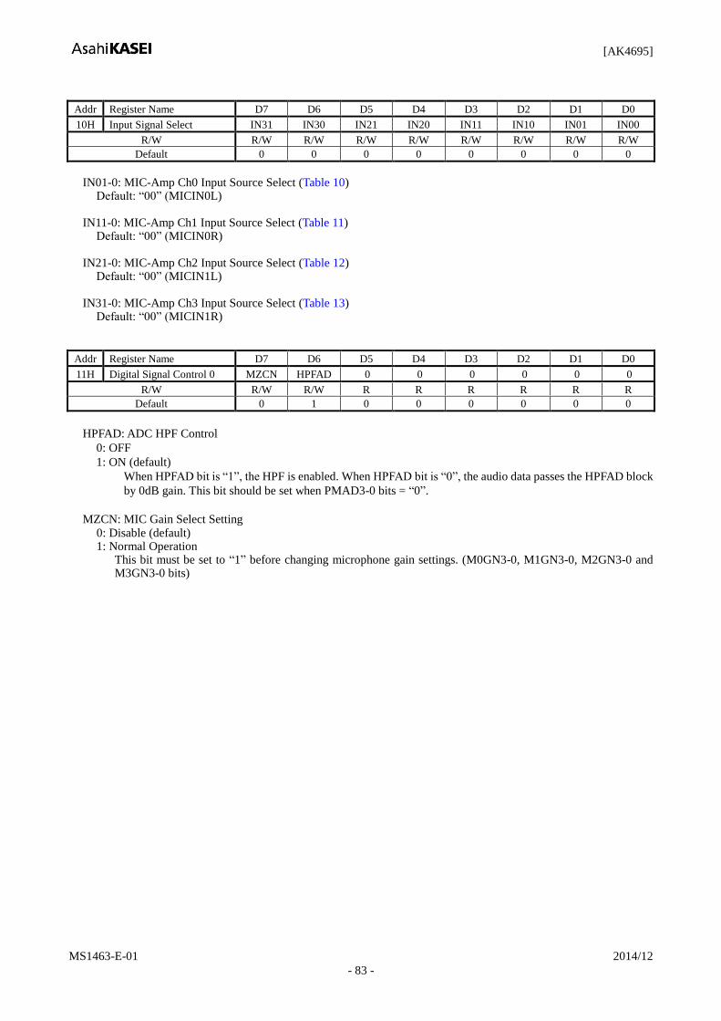
[AK4695]
MS1463-E-01 2014/12
- 83 -
Addr Register Name D7 D6 D5 D4 D3 D2 D1 D0
10H Input Signal Select IN31 IN30 IN21 IN20 IN11 IN10 IN01 IN00
R/W R/W R/W R/W R/W R/W R/W R/W R/W
Default 0 0 0 0 0 0 0 0
IN01-0: MIC-Amp Ch0 Input Source Select (Table 10)
Default: “00” (MICIN0L) IN11-0: MIC-Amp Ch1 Input Source Select (Table 11)
Default: “00” (MICIN0R) IN21-0: MIC-Amp Ch2 Input Source Select (Table 12)
Default: “00” (MICIN1L) IN31-0: MIC-Amp Ch3 Input Source Select (Table 13)
Default: “00” (MICIN1R)
Addr Register Name D7 D6 D5 D4 D3 D2 D1 D0
11H Digital Signal Control 0 MZCN HPFAD 0 0 0 0 0 0
R/W R/W R/W R R R R R R
Default 0 1 0 0 0 0 0 0
HPFAD: ADC HPF Control
0: OFF
1: ON (default)
When HPFAD bit is “1”, the HPF is enabled. When HPFAD bit is “0”, the audio data passes the HPFAD block
by 0dB gain. This bit should be set when PMAD3-0 bits = “0”.
MZCN: MIC Gain Select Setting 0: Disable (default)
1: Normal Operation This bit must be set to “1” before changing microphone gain settings. (M0GN3-0, M1GN3-0, M2GN3-0 and M3GN3-0 bits)

[AK4695]
MS1463-E-01 2014/12
- 84 -
Addr Register Name D7 D6 D5 D4 D3 D2 D1 D0
12H Digital Signal Control 1 DACBS1 DACBS0 DRCENB DRCENA DASEL1 DASEL0 PFSDO PFSEL
R/W R/W R/W R/W R/W R/W R/W R/W R/W
Default 0 0 1 1 0 0 1 0
PFSEL: Programmable Filter Block Input Signal Select (Table 33)
0: ADC Output Data (default)
1: SDTI Input Data
PFSDO: SDTO1, 2 Input Signal Select (Table 34)
0: ADC Output Data
1: Programmable Filter Block Output Data (default)
DASEL1-0: DACA/B, DRC Input Signal Select (Table 35)
Default: “00” (SDTI)
DRCENA: DACA Input Signal Select (Table 36)
0: DASEL1-0 bits Output Data
1: DRC Output Data (default)
DRCENB: DACB Input Signal Select (Table 37)
0: DASEL1-0 bits Output Data
1: DRC Output Data (default)
DACBS1-0: DACB Input Channel Select (Table 38)
Default: “00”

[AK4695]
MS1463-E-01 2014/12
- 85 -
Addr Register Name D7 D6 D5 D4 D3 D2 D1 D0
13H Lineout & HP Control HPZ 0 0 DACS BEEPS LOPSB LOPSA LBSEL
R/W R/W R R R/W R/W R/W R/W R/W
Default 0 0 0 0 0 0 0 0
LBSEL: Speaker Output and Stereo Line Output B Switching
0: Speaker Output (SPP/SPN pins) (default)
1: Stereo Line Output B (LOUTB/ROUTB pins)
LOPSA: Stereo Line Output A Power-save Mode
0: Normal Operation (default)
1: Standby
LOPSB: Stereo Line Output B Power-save Mode
0: Normal Operation (default)
1: Standby
This bit is enabled when LBSEL bit = “1”.
BEEPS: Signal Control of “BEEPIN pin → Speaker Output/Stereo Line Output B”
0: OFF (default)
1: ON
This bit is enabled when PMSPLO bits = “1”.
DACS: Signal Control of “DACB → Speaker Output/Stereo Line Output B”
0: OFF (default)
1: ON
HPZ: HP-Amp Pull-down Setting (Table 75)
0: Pulled-down by 10 (typ) (default)
1: Hi-Z

[AK4695]
MS1463-E-01 2014/12
- 86 -
Addr Register Name D7 D6 D5 D4 D3 D2 D1 D0
14H ALC Mode Control 0 0 RGAIN2 RGAIN1 RGAIN0 WTM1 WTM0 LMTH1 LMTH0
R/W R R/W R/W R/W R/W R/W R/W R/W
Default 0 0 0 0 0 0 0 0
LMTH1-0: ALC Limiter Detection Lavel / Recovery Wait Counter Reset Level (Table 22)
Default: “00”
WTM1-0: ALC Recovery Wait Time Setting (Table 24)
These bits set a period of recovery operation when any limiter operation does not occur during ALC operation.
The default value is “00” (128f/fs).
RGAIN2-0: ALC Recovery Gain Setting (Table 25)
Default: “000” (0.00424dB)
RFATT: Attenuation Step Setting of ALC First Recovery Reference Volume (Table 28)
0: -0.00106dB (4/fs) (default)
1: -0.00106dB (16/fs)
Addr Register Name D7 D6 D5 D4 D3 D2 D1 D0
15H ALC Mode Control 1 0 0 0 0 ALCEQN ATTLMT RFST1 RFST0
R/W R R R R R/W R/W R/W R/W
Default 0 0 0 0 0 0 0 0
RFST1-0: ALC First Recovery Gain Setting (Table 27)
Default: “00” (0.0032dB)
ATTLMT: ALC Attenuation Limit Setting
0: No Limit (default)
1: 0dB Limit
ALCEQN: ALC EQ Control
0: ALC EQ On (default)
1: ALC EQ Off

[AK4695]
MS1463-E-01 2014/12
- 87 -
Addr Register Name D7 D6 D5 D4 D3 D2 D1 D0
16H HPF1, 2 Control HPF23 HPF22 HPF21 HPF20 HPF13 HPF12 HPF11 HPF10
R/W R/W R/W R/W R/W R/W R/W R/W R/W
Default 0 0 0 0 0 0 0 0
HPF13-0: HPF1 Coefficient Setting Enable
0: Disable (default)
1: Enable
When HPF1x bit is “1”, the settings of HPF1A13-0 bits and HPF1B13-0 bits are valid. When HPF1x bit is “0”,
the audio data of a correspondent channel passes the HPF1 block by 0dB gain. (x=3~0)
HPF23-0: HPF2 Coefficient Setting Enable
0: Disable (default)
1: Enable
When HPF2x bit is “1”, the settings of HPF2A13-0 bits and HPF2B13-0 bits are valid. When HPF2x bit is “0”,
the audio data of a correspondent channel passes the HPF2 block by 0dB gain. (x=3~0)
Addr Register Name D7 D6 D5 D4 D3 D2 D1 D0
17H ALC & LPF1 Control ALC3 ALC2 ALC1 ALC0 LPF13 LPF12 LPF11 LPF10
R/W R/W R/W R/W R/W R/W R/W R/W R/W
Default 0 0 0 0 0 0 0 0
LPF13-0: LPF1 Coefficient Setting Enable
0: Disable (default)
1: Enable
When LPF1x bit is “1”, the settings of LPF1A13-0 bits and LPF1B13-0 bits are valid. When LPF1x bit is “0”,
the audio data of a correspondent channel passes the LPF1 block by 0dB gain. (x=3~0)
ALC3-0: ALC Setting Enable
0: ALC Disable (default)
1: ALC Enable
Addr Register Name D7 D6 D5 D4 D3 D2 D1 D0
18H EQ1, 2 Control EQ23 EQ22 EQ21 EQ20 EQ13 EQ12 EQ11 EQ10
R/W R/W R/W R/W R/W R/W R/W R/W R/W
Default 0 0 0 0 0 0 0 0
EQ13-0: EQ1 Coefficient Setting Enable
0: Disable (default)
1: Enable
When EQ1x bit is “1”, the settings of EQ1A15-0, EQ1B15-0 and EQ1C15-0 bits are valid. When EQ1x bit is
“0”, the audio data of a correspondent channel passes the EQ1 block by 0dB gain. (x=3~0)
EQ23-0: EQ2 Coefficient Setting Enable
0: Disable (default)
1: Enable
When EQ2x bit is “1”, the settings of EQ2A15-0, EQ2B15-0 and EQ2C15-0 bits are valid. When EQ2x bit is
“0”, the audio data of a correspondent channel passes the EQ2 block by 0dB gain. (x=3~0)

[AK4695]
MS1463-E-01 2014/12
- 88 -
Addr Register Name D7 D6 D5 D4 D3 D2 D1 D0
19H Power Management 0 PMMPB PMMPA 0 MMODE PMAD3 PMAD2 PMAD1 PMAD0
R/W R/W R/W R R/W R/W R/W R/W R/W
Default 0 0 0 0 0 0 0 0
PMAD3-0: Power Management of MIC-Amp & ADC Ch0/1/2/3
0: Power down (default)
1: Power up
When the PMADx is changed from “0” to “1”, the initialization cycle (1059/fs=22.1ms @48kHz, ADRST bit =
“0”) starts. After initializing, ADC digital data is output. (x=3~0)
MMODE: MIC-Amp Mode Setting
0: Test Mode (default)
1: Normal Operation
MMODE bit must be written “1”.
PMMPA: MPWRA pin Power Management
0: Power down: Hi-Z (default)
1: Power up
PMMPB: MPWRB pin Power Management
0: Power down: Hi-Z (default)
1: Power up
Addr Register Name D7 D6 D5 D4 D3 D2 D1 D0
1AH Power Management 1 PMDRC 0 0 PMDSP PMPFIL3 PMPFIL2 PMPFIL1 PMPFIL0
R/W R/W R R R/W R/W R/W R/W R/W
Default 0 0 0 0 0 0 0 0
PMPFIL3-0: Power Management of Programmable Filter Block 0/1/2/3
0: Power down (default)
1: Power up
PMDSP: DSP Block Power Management
0: Power down (default)
1: Power up
PMDRC: Dynamic Range Control Block Power Management
0: Power down (default)
1: Power up

[AK4695]
MS1463-E-01 2014/12
- 89 -
Addr Register Name D7 D6 D5 D4 D3 D2 D1 D0
1BH Power Management 2 0 PMBP PMHPR PMHPL PMLO PMSPLO PMDACB PMDACA
R/W R R/W R/W R/W R/W R/W R/W R/W
Default 0 0 0 0 0 0 0 0
PMDACA: DACA Power Management
0: Power down (default)
1: Power up
PMDACB: DACB Power Management
0: Power down (default)
1: Power up
PMSPLO: Power Management of Speaker-Amp and Stereo Line Output B
0: Power down (default)
1: Power up
PMLO: Stereo Line Output A Power Management
0: Power down (default)
1: Power up
PMHPL: Headphone Lch Power Management
0: Power down (default)
1: Power up
PMHPR: Headphone Rch Power Management
0: Power down (default)
1: Power up
PMBP: BEEP Input Power Management
0: Power down (default)
1: Power up
Addr Register Name D7 D6 D5 D4 D3 D2 D1 D0
1CH Power Management 3 PMDM3 PMDM2 PMDM1 PMDM0 0 0 0 LMODE
R/W R/W R/W R/W R/W R R R R/W
Default 0 0 0 0 0 0 0 1
LMODE: Power-save Mode Select of Stereo Line Output A (Table 73, Table 74)
0: Using a same connector for both Line input and output
1: Line output and input are independent (default)
PMDM3-0: Input Signal Select with Digital Microphone (Table 8, Table 9)
0: Power down (default)
1: Power up These bits are enabled when DMIC bit = “1”. ADC digital block is powered-down by PMDM3-0 bits = “0” when selecting a digital microphone input (DMIC bit = “1”).
Each block can be powered-down respectively by writing “0” in each bit of the address 19H~1CH. When the PDN pin
is “L”, all blocks are powered-down regardless of setting of these addresses. In this case, register is initialized to the
default value.
When all power management bits are “0”, all blocks are powered-down. The register values remain unchanged. Power
supply current is 50μA(typ) in this case. For fully shut down (typ. 0μA), the PDN pin should be “L”.
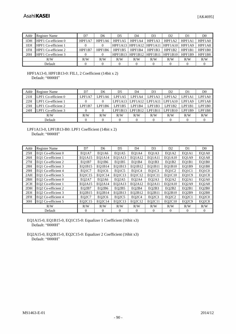
[AK4695]
MS1463-E-01 2014/12
- 90 -
Addr Register Name D7 D6 D5 D4 D3 D2 D1 D0
1DH HPF1 Co-efficient 0 HPF1A7 HPF1A6 HPF1A5 HPF1A4 HPF1A3 HPF1A2 HPF1A1 HPF1A0
1EH HPF1 Co-efficient 1 0 0 HPF1A13 HPF1A12 HPF1A11 HPF1A10 HPF1A9 HPF1A8
1FH HPF1 Co-efficient 2 HPF1B7 HPF1B6 HPF1B5 HPF1B4 HPF1B3 HPF1B2 HPF1B1 HPF1B0
20H HPF1 Co-efficient 3 0 0 HPF1B13 HPF1B12 HPF1B11 HPF1B10 HPF1B9 HPF1B8
R/W R/W R/W R/W R/W R/W R/W R/W R/W
Default 0 0 0 0 0 0 0 0
HPF1A13-0, HPF1B13-0: FIL1, 2 Coefficient (14bit x 2) Default: “0000H”
Addr Register Name D7 D6 D5 D4 D3 D2 D1 D0
21H LPF1 Co-efficient 0 LPF1A7 LPF1A6 LPF1A5 LPF1A4 LPF1A3 LPF1A2 LPF1A1 LPF1A0
22H LPF1 Co-efficient 1 0 0 LPF1A13 LPF1A12 LPF1A11 LPF1A10 LPF1A9 LPF1A8
23H LPF1 Co-efficient 2 LPF1B7 LPF1B6 LPF1B5 LPF1B4 LPF1B3 LPF1B2 LPF1B1 LPF1B0
24H LPF1 Co-efficient 3 0 0 LPF1B13 LPF1B12 LPF1B11 LPF1B10 LPF1B9 LPF1B8
R/W R/W R/W R/W R/W R/W R/W R/W R/W
Default 0 0 0 0 0 0 0 0
LPF1A13-0, LPF1B13-B0: LPF1 Coefficient (14bit x 2)
Default: “0000H”
Addr Register Name D7 D6 D5 D4 D3 D2 D1 D0
25H EQ1 Co-efficient 0 EQ1A7 EQ1A6 EQ1A5 EQ1A4 EQ1A3 EQ1A2 EQ1A1 EQ1A0
26H EQ1 Co-efficient 1 EQ1A15 EQ1A14 EQ1A13 EQ1A12 EQ1A11 EQ1A10 EQ1A9 EQ1A8
27H EQ1 Co-efficient 2 EQ1B7 EQ1B6 EQ1B5 EQ1B4 EQ1B3 EQ1B2 EQ1B1 EQ1B0
28H EQ1 Co-efficient 3 EQ1B15 EQ1B14 EQ1B13 EQ1B12 EQ1B11 EQ1B10 EQ1B9 EQ1B8
29H EQ1 Co-efficient 4 EQ1C7 EQ1C6 EQ1C5 EQ1C4 EQ1C3 EQ1C2 EQ1C1 EQ1C0
2AH EQ1 Co-efficient 5 EQ1C15 EQ1C14 EQ1C13 EQ1C12 EQ1C11 EQ1C10 EQ1C9 EQ1C8
2BH EQ2 Co-efficient 0 EQ2A7 EQ2A6 EQ2A5 EQ2A4 EQ2A3 EQ2A2 EQ2A1 EQ2A0
2CH EQ2 Co-efficient 1 EQ2A15 EQ2A14 EQ2A13 EQ2A12 EQ2A11 EQ2A10 EQ2A9 EQ2A8
2DH EQ2 Co-efficient 2 EQ2B7 EQ2B6 EQ2B5 EQ2B4 EQ2B3 EQ2B2 EQ2B1 EQ2B0
2EH EQ2 Co-efficient 3 EQ2B15 EQ2B14 EQ2B13 EQ2B12 EQ2B11 EQ2B10 EQ2B9 EQ2B8
2FH EQ2 Co-efficient 4 EQ2C7 EQ2C6 EQ2C5 EQ2C4 EQ2C3 EQ2C2 EQ2C1 EQ2C0
30H EQ2 Co-efficient 5 EQ2C15 EQ2C14 EQ2C13 EQ2C12 EQ2C11 EQ2C10 EQ2C9 EQ2C8
R/W R/W R/W R/W R/W R/W R/W R/W R/W
Default 0 0 0 0 0 0 0 0
EQ1A15-0, EQ1B15-0, EQ1C15-0: Equalizer 1 Coefficient (16bit x3)
Default: “0000H”
EQ2A15-0, EQ2B15-0, EQ2C15-0: Equalizer 2 Coefficient (16bit x3)
Default: “0000H”

[AK4695]
MS1463-E-01 2014/12
- 91 -
Addr Register Name D7 D6 D5 D4 D3 D2 D1 D0
31H DRC Mode Control 0 DLMAT2 DLMAT1 DLMAT0 DRGAIN1 DRGAIN0 DRCC1 DRCC0
R/W R R/W R/W R/W R/W R/W R/W R/W
Default 0 0 0 0 0 0 0 0
DRCC1-0: DRC Setting Enable (Table 63)
00: Disable (default)
01: Low
10: Middle
11: High
When DRCC1-0 bits = “00”, the audio data passes the DRC block by 0dB gain.
DRGAIN1-0: DRC Recovery Speed Setting (Table 65)
Default: “00”
DLMAT1-0: DRC Attenuation Speed Setting (Table 64)
Default: “000”
Addr Register Name D7 D6 D5 D4 D3 D2 D1 D0
32H NS Control 0 0 DRCM1 DRCM0 0 NSLPF NSHPF NSCE
R/W R R R/W R/W R R/W R/W R/W
Default 0 0 0 0 0 0 0 0
NSCE: Noise Suppression Setting Enable
0: Disable (default)
1: Enable
When NSCE bit = “0”, the audio data passes Noise Suppression block by 0dB gain.
NSHPF: HPF Coefficient Setting Enable of the Noise Suppression Block
0: Disable (default)
1: Enable
When NSHPF bit is “1”, the settings of NSHA13-0 bits and NSHB13-0 bits are valid. When NSHPF bit is “0”,
the audio data passes the HPF block by 0dB gain.
NSLPF: LPF Coefficient Setting Enable of the Noise Suppression Block
0: Disable (default)
1: Enable
When NSLPF bit is “1”, the settings of NSLA13-0 bits and NSLB13-0 bits are valid. When NSLPF bit is “0”,
the audio data passes the LPF block by 0dB gain.
DRCM1-0: DRC Input Signal Setting (Table 39)
Default: “00” (L = Lch, R = Rch)
Addr Register Name D7 D6 D5 D4 D3 D2 D1 D0
33H NS Gain & ATT Control 0 NSGAIN2 NSGAIN1 NSGAIN0 0 NSATT2 NSATT1 NSATT0
R/W R R/W R/W R/W R R/W R/W R/W
Default 0 0 0 1 0 0 0 1
NSATT2-0: Noise Suppression Attenuation Speed Setting (Table 43)
Default: “001”
NSGAIN2-0: Noise Suppression Recovery Speed Setting (Table 46)
Default: “001”

[AK4695]
MS1463-E-01 2014/12
- 92 -
Addr Register Name D7 D6 D5 D4 D3 D2 D1 D0
34H NS On Level NSIAF1 NSIAF0 0 NSTHL4 NSTHL3 NSTHL2 NSTHL1 NSTHL0
R/W R/W R/W R R/W R/W R/W R/W R/W
Default 1 0 0 0 0 0 0 0
NSTHL4-0: Noise Suppression Threshold Low Level Setting (Table 41)
Default: “00H” (-36dB)
NSIAF1-0: Moving Avarage Parameter Setting at Noise Suppression Off (Table 40)
Default: “10” (1024/fs)
Addr Register Name D7 D6 D5 D4 D3 D2 D1 D0
35H NS Off Level NSOAF1 NSOAF0 0 NSTHH4 NSTHH3 NSTHH2 NSTHH1 NSTHH0
R/W R/W R/W R R/W R/W R/W R/W R/W
Default 1 0 0 0 0 0 0 0
NSTHH4-0: Noise Suppression Threshold High Level Setting (Table 45)
Default: “00H” (-36dB)
NSOAF1-0: Moving Avarage Parameter Setting at Noise Suppression ON (Table 44)
Default: “10” (16/fs)
Addr Register Name D7 D6 D5 D4 D3 D2 D1 D0
36H NS Reference Select 0 0 0 0 NSREF3 NSREF2 NSREF1 NSREF0
R/W R R R R R/W R/W R/W R/W
Default 0 0 0 0 0 0 0 0
NSREF3-0: Noise Suppression Reference Level Setting (Table 42)
Default: “0H” (-9dB)
Addr Register Name D7 D6 D5 D4 D3 D2 D1 D0
37H NS LPF Co-efficient 0 NSLA7 NSLA6 NSLA5 NSLA4 NSLA3 NSLA2 NSLA1 NSLA0
38H NS LPF Co-efficient 1 0 0 NSLA13 NSLA12 NSLA11 NSLA10 NSLA9 NSLA8
39H NS LPF Co-efficient 2 NSLB7 NSLB6 NSLB5 NSLB4 NSLB3 NSLB2 NSLB1 NSLB0
3AH NS LPF Co-efficient 3 0 0 NSLB13 NSLB12 NSLB11 NSLB10 NSLB9 NSLB8
3BH NS HPF Co-efficient 0 NSHA7 NSHA6 NSHA5 NSHA4 NSHA3 NSHA2 NSHA1 NSHA0
3CH NS HPF Co-efficient 1 0 0 NSHA13 NSHA12 NSHA11 NSHA10 NSHA9 NSHA8
3DH NS HPF Co-efficient 2 NSHB7 NSHB6 NSHB5 NSHB4 NSHB3 NSHB2 NSHB1 NSHB0
3EH NS HPF Co-efficient 3 0 0 NSHB13 NSHB12 NSHB11 NSHB10 NSHB9 NSHB8
R/W R/W R/W R/W R/W R/W R/W R/W R/W
Default 0 0 0 0 0 0 0 0
NSLA13-0, NSLB13-0: Noise Suppression LPF Coefficient (14bit x 2)
Default: “0000H”
NSHA13-0, NSHB13-0: Noise Suppression HPF Coefficient (14bit x 2)
Default: “0000H”

[AK4695]
MS1463-E-01 2014/12
- 93 -
Addr Register Name D7 D6 D5 D4 D3 D2 D1 D0
3FH DVLC Filter Select DLLPF1 DLLPF0 DMHPF1 DMHPF0 DMLPF1 DMLPF0 DHHPF1 DHHPF0
R/W R/W R/W R/W R/W R/W R/W R/W R/W
Default 0 0 0 0 0 0 0 0
DHHPF1-0: DVLC High Frequency Range HPF Coefficient Setting Enable (Table 56)
00: Disable (default)
01: 1st order HPF
10: 2nd order HPF
11: N/A (Not Available)
When DHHPF1-0 bits are “01” or “10”, the settings of DHHA13-0 and DHHB13-0 bits are enabled. When
DHHPF1-0 bits are “00”, the HPF block outputs “0” data.
DMLPF1-0: DVLC Middle Frequency Range LPF Coefficient Setting Enable (Table 52)
00: Disable (default)
01: 1st order LPF
10: 2nd order LPF
11: N/A (Not Available)
When DMLPF1-0 bits are “01” or “10”, the settings of DMLA13-0 and DMLB13-0 bits are enabled. When
DMLPF1-0 bits are “00”, the audio data passes DVLC middle frequency range of the LPF by 0dB gain.
DMHPF1-0: DVLC Middle Frequency Range HPF Coefficient Setting Enable (Table 51)
00: Disable (default)
01: 1st order HPF
10: 2nd order HPF
11: N/A (Not Available)
When DMHPF1-0 bits are “01” or “10”, the setting of DMHA13-0 and DMHB13-0 bits are enabled. When
DMHPF1-0 bits are “00”, the audio data passes DVLC middle frequency range of the HPF by 0dB gain.
DLLPF1-0: DVLC Low Frequency Range LPF Coefficient Setting Enable (Table 47)
00: Disable (default)
01: 1st order LPF
10: 2nd order LPF
11: N/A (Not Available)
When DLLPF1-0 bits are “01” or “10”, the settings of DLLA13-0 and DLLB13-0 bits are enabled. When
DLLPF1-0 bits are “00”, LPF block outputs “0” data.
Addr Register Name D7 D6 D5 D4 D3 D2 D1 D0
40H DVLC Mode Control DVRGAIN2 DVRGAIN1 DVRGAIN0 DVLMAT2 DVLMAT1 DVLMAT0 DAF1 DAF0
R/W R/W R/W R/W R/W R/W R/W R/W R/W
Default 0 1 1 0 1 1 1 1
DAF1-0: Moving Avarage Parameter Setting for DVLC (Table 60)
Default: “11” (Default: 2048/fs)
DVLMAT2-0: DVLC Attenuation Speed Setting (Table 61)
Default: “011”
DVRGAIN2-0: DVLC Recovery Speed Setting (Table 62)
Default: “011”

[AK4695]
MS1463-E-01 2014/12
- 94 -
Addr Register Name D7 D6 D5 D4 D3 D2 D1 D0
41H DVLCL Curve X1 0 0 VL1X5 VL1X4 VL1X3 VL1X2 VL1X1 VL1X0
42H DVLCL Curve Y1 0 0 VL1Y5 VL1Y4 VL1Y3 VL1Y2 VL1Y1 VL1Y0
43H DVLCL Curve X2 0 0 VL2X5 VL2X4 VL2X3 VL2X2 VL2X1 VL2X0
44H DVLCL Curve Y2 0 0 VL2Y5 VL2Y4 VL2Y3 VL2Y2 VL2Y1 VL2Y0
45H DVLCL Curve X3 0 0 0 VL3X4 VL3X3 VL3X2 VL3X1 VL3X0
46H DVLCL Curve Y3 0 0 0 VL3Y4 VL3Y3 VL3Y2 VL3Y1 VL3Y0
47H DVLCL Slope 1 0 L1G6 L1G5 L1G4 L1G3 L1G2 L1G1 L1G0
48H DVLCL Slope 2 0 L2G6 L2G5 L2G4 L2G3 L2G2 L2G1 L2G0
49H DVLCL Slope 3 0 L3G6 L3G5 L3G4 L3G3 L3G2 L3G1 L3G0
4AH DVLCL Slope 4 0 L4G6 L4G5 L4G4 L4G3 L4G2 L4G1 L4G0
4BH DVLCM Curve X1 0 0 VM1X5 VM1X4 VM1X3 VM1X2 VM1X1 VM1X0
4CH DVLCM Curve Y1 0 0 VM1Y5 VM1Y4 VM1Y3 VM1Y2 VM1Y1 VM1Y0
4DH DVLCM Curve X2 0 0 VM2X5 VM2X4 VM2X3 VM2X2 VM2X1 VM2X0
4EH DVLCM Curve Y2 0 0 VM2Y5 VM2Y4 VM2Y3 VM2Y2 VM2Y1 VM2Y0
4FH DVLCM Curve X3 0 0 0 VM3X4 VM3X3 VM3X2 VM3X1 VM3X0
50H DVLCM Curve Y3 0 0 0 VM3Y4 VM3Y3 VM3Y2 VM3Y1 VM3Y0
51H DVLCM Slope 1 0 M1G6 M1G5 M1G4 M1G3 M1G2 M1G1 M1G0
52H DVLCM Slope 2 0 M2G6 M2G5 M2G4 M2G3 M2G2 M2G1 M2G0
53H DVLCM Slope 3 0 M3G6 M3G5 M3G4 M3G3 M3G2 M3G1 M3G0
54H DVLCM Slope 4 0 M4G6 M4G5 M4G4 M4G3 M4G2 M4G1 M4G0
55H DVLCH Curve X1 0 0 VH1X5 VH1X4 VH1X3 VH1X2 VH1X1 VH1X0
56H DVLCH Curve Y1 0 0 VH1Y5 VH1Y4 VH1Y3 VH1Y2 VH1Y1 VH1Y0
57H DVLCH Curve X2 0 0 VH2X5 VH2X4 VH2X3 VH2X2 VH2X1 VH2X0
58H DVLCH Curve Y2 0 0 VH2Y5 VH2Y4 VH2Y3 VH2Y2 VH2Y1 VH2Y0
59H DVLCH Curve X3 0 0 0 VH3X4 VH3X3 VH3X2 VH3X1 VH3X0
5AH DVLCH Curve Y3 0 0 0 VH3Y4 VH3Y3 VH3Y2 VH3Y1 VH3Y0
5BH DVLCH Slope 1 0 H1G6 H1G5 H1G4 H1G3 H1G2 H1G1 H1G0
5CH DVLCH Slope 2 0 H2G6 H2G5 H2G4 H2G3 H2G2 H2G1 H2G0
5DH DVLCH Slope 3 0 H3G6 H3G5 H3G4 H3G3 H3G2 H3G1 H3G0
5EH DVLCH Slope 4 0 H4G6 H4G5 H4G4 H4G3 H4G2 H4G1 H4G0
R/W R R/W R/W R/W R/W R/W R/W R/W
Default 0 0 0 0 0 0 0 0
VL1X5-0, VL2X5-0, VL3X4-0: Input Gain Setting of Low Range DVLC Point (Table 48, Table 49)
Default: “00H” (0dB)
VL1Y5-0, VL2Y5-0, VL3Y4-0: Output Gain Setting of Low Range DVLC Point (Table 48, Table 49)
Default: “00H” (0dB)
L1G6-0, L2G6-0, L3G6-0, L4G6-0: Low Range DVLC Slope Setting (Table 50)
Default: “00H”
VM1X5-0, VM2X5-0, VM3X4-0: Input Gain Setting of Middle Range DVLC Point (Table 53, Table 54)
Default: “00H” (0dB)
VM1Y5-0, VM2Y5-0, VM3Y4-0: Output Gain Setting of Middle Range DVLC Point (Table 53, Table 54)
Default: “00H” (0dB)
M1G6-0, M2G6-0, M3G6-0, M4G6-0: Middle Range DVLC Slope Setting (Table 55)
Default: “00H”
VH1X5-0, VH2X5-0, VH3X4-0: Input Gain Setting of High Range DVLC Point (Table 57, Table 58)
Default: “00H” (0dB)
VH1Y5-0, VH2Y5-0, VH3Y4-0: Output Gain Setting of High Range DVLC Point (Table 57, Table 58)
Default: “00H” (0dB)
H1G6-0, H2G6-0, H3G6-0, H4G6-0: High Range DVLC Slope Setting (Table 59)
Default: “00H”

[AK4695]
MS1463-E-01 2014/12
- 95 -
Addr Register Name D7 D6 D5 D4 D3 D2 D1 D0
5FH DVLCL LPF Co-efficient 0 DLLA7 DLLA6 DLLA5 DLLA4 DLLA3 DLLA2 DLLA1 DLLA0
60H DVLCL LPF Co-efficient 1 0 0 DLLA13 DLLA12 DLLA11 DLLA10 DLLA9 DLLA8
61H DVLCL LPF Co-efficient 2 DLLB7 DLLB6 DLLB5 DLLB4 DLLB3 DLLB2 DLLB1 DLLB0
62H DVLCL LPF Co-efficient 3 0 0 DLLB13 DLLB12 DLLB11 DLLB10 DLLB9 DLLB8
63H DVLCM HPF Co-efficient 0 DMHA7 DMHA6 DMHA5 DMHA4 DMHA3 DMHA2 DMHA1 DMHA0
64H DVLCM HPF Co-efficient 1 0 0 DMHA13 DMHA12 DMHA11 DMHA10 DMHA9 DMHA8
65H DVLCM HPF Co-efficient 2 DMHB7 DMHB6 DMHB5 DMHB4 DMHB3 DMHB2 DMHB1 DMHB0
66H DVLCM HPF Co-efficient 3 0 0 DMHB13 DMHB12 DMHB11 DMHB10 DMHB9 DMHB8
67H DVLCM LPF Co-efficient 0 DMLA7 DMLA6 DMLA5 DMLA4 DMLA3 DMLA2 DMLA1 DMLA0
68H DVLCM LPF Co-efficient 1 0 0 DMLA13 DMLA12 DMLA11 DMLA10 DMLA9 DMLA8
69H DVLCM LPF Co-efficient 2 DMLB7 DMLB6 DMLB5 DMLB4 DMLB3 DMLB2 DMLB1 DMLB0
6AH DVLCM LPF Co-efficient 3 0 0 DMLB13 DMLB12 DMLB11 DMLB10 DMLB9 DMLB8
6BH DVLCH HPF Co-efficient 0 DHHA7 DHHA6 DHHA5 DHHA4 DHHA3 DHHA2 DHHA1 DHHA0
6CH DVLCH HPF Co-efficient 1 0 0 DHHA13 DHHA12 DHHA11 DHHA10 DHHA9 DHHA8
6DH DVLCH HPF Co-efficient 2 DHHB7 DHHB6 DHHB5 DHHB4 DHHB3 DHHB2 DHHB1 DHHB0
6EH DVLCH HPF Co-efficient 3 0 0 DHHB13 DHHB12 DHHB11 DHHB10 DHHB9 DHHB8
R/W R/W R/W R/W R/W R/W R/W R/W R/W
Default 0 0 0 0 0 0 0 0
DLLA13-0, DLLB13-0: DVLC Low Frequency Range LPF Coefficient (14bit x 2)
Default: “0000H”
DMHA13-0, DMHB13-0: DVLC Middle Frequency Range HPF Coefficient (14bit x 2)
Default: “0000H”
DMLA13-0, DMLB13-0: DVLC Middle Frequency Range LPF Coefficient (14bit x 2)
Default: “0000H”
DHHA13-0, DHHB13-0: DVLC High Frequency Range HPF Coefficient (14bit x 2)
Default: “0000H”

[AK4695]
MS1463-E-01 2014/12
- 96 -
SYSTEM DESIGN
Figure 55 shows the system connection diagram. An evaluation board (AKD4695) is available for fast evaluation as well as
suggestions for peripheral circuitry.
IN0
Cap-less Headphone
Speaker
MPWRB
MICIN0L /DDAT
MICIN0R /DMCLK
MICIN1L /DDAT1
MICIN1R
SPP/LOUTB
SPN/ROUTB
SVDD
AVDD VSS1 TVDD
CCLK
CDTIO
BCKI
LRCK
SDTO1
SDTI
MCKI
HPL
HPR
VSS3
CSN
PDN
MICIN2L
MICIN2R
PVEE CP CN
MPWRA
VCOM DVDD
GPO1
SDTO2
Line In
AUXINL
AUXINR
MICIN3L
MICIN3R
IN1
IN2
IN3
BEEPIN Beep In
Stereo Line-out
LOUTA
ROUTA
MRF
2.2k x 4
1u x 10
0.22u 0.22u
100 100
10u Power Supply
2.7 3.5V 0.1u
2.2u 2.2u
0.1u 1u 1u 0.1u 0.1u
10u Power Supply
2.7 3.5V 10u
Power Supply
1.6 2.0V
10u
Power Supply
1.6 3.5V
AK4695
1k
1k
22k 22k
1u
1u
Analog Ground
Digital Ground
DSP
P
VSS2
1k x 4
0.1u
1n x 10
Note:
- VSS1, VSS2 and VSS3 of the AK4695 must be distributed separately from the ground of external controllers.
- All digital input pins must not be allowed to float.
- 0.1F capacitors at power supply pins should be ceramic capacitors. Other capacitors do not have specific
types.
Figure 55. System Connection Diagram

[AK4695]
MS1463-E-01 2014/12
- 97 -
1. Grounding and Power Supply Decoupling
The AK4695 requires careful attention to power supply and grounding arrangements. AVDD and SVDD are usually
supplied from the system’s analog supply, and DVDD and TVDD are supplied from the system’s digital power supply. If
AVDD, DVDD, TVDD and SVDD are supplied separately, the power-up sequence is not critical. The PDN pin should be
held “L” when power supplies are tuning on. The PDN pin is allowed to be “H” after all power supplies are applied and
settled.
To avoid pop noise on headphone output and line output when power up/down, the AK4695 should be operated along the
following recommended power-up/down sequence.
1) Power-up
- The PDN pin should be held “L” when power supplies are turning on. The AK4695 can be reset by keeping the PDN
pin “L” for 1.5μs or longer after all power supplies are applied and settled.
2) Power-down
- Each of power supplies can be powered OFF after the PDN pin is set to “L”.
VSS1, VSS2 and VSS3 of the AK4695 should be connected to the analog ground plane. System analog ground and digital
ground should be wired separately and connected together as close as possible to where the supplies are brought onto the
printed circuit board. Decoupling capacitors should be as close the power supply pins as possible. Especially, the small
value ceramic capacitor is to be closest.
2. Voltage Reference
VCOM is a signal ground of this chip. A 1μF ceramic capacitor connected to the VCOM pin eliminates the effects of high
frequency noise. It should be connected as close as possible to the VCOM pin. No load current is allowed to be drawn from
the VCOM pin. All signals, especially clocks, should be kept away from the VCOM pin in order to avoid unwanted
coupling into the AK4695.
3. Charge Pump
2.2μF±50% capacitors between the CP and CN pins, and the VEE and VSS3 pins should be low ESR ceramic capacitors.
These capacitors must be connected as close as possible to the pins. No load current may be drawn from the VEE pin.
4. Analog Inputs
The MIC input is single-ended. The input signal range scales with typ. (0.566 x AVDD) Vpp (@ MGAIN = +3dB),
centered around the internal common voltage (typ. (0.5 x AVDD) V). Usually the input signal is AC coupled using a
capacitor (1μF or less is recommended). The cut-off frequency is fc = 1/(2RC). Connect a 1nF capacitor between each
analog input and VSS1 for stabilized characteristics.
5. Analog Outputs
The stereo line output A is centered on typ. (0.5 x AVDD) V. They (LOUTA/ROUTA pins) must be AC-coupled using a
capacitor. The headphone output is single-ended and centered around VSS (0V). There is no need for AC coupling
capacitors. The speaker outputs (SPP/SPN pins) are centered on SVDD/2 (typ.), and they should be connected directly to
a speaker. There is no need for AC coupling capacitors. The stereo line outputs B (LOUTB/ROUTB pins) are centered on
typ. (0.5 x AVDD) V. These pins must be AC-coupled using a capacitor.

[AK4695]
MS1463-E-01 2014/12
- 98 -
CONTROL SEQUENCE
Clock Set up
When ADC, DAC or Programmable filters are powered-up, the clocks must be supplied.
(1)
Power Supply
PDN pin
PMVCM bit(Addr:01H, D7)
(2) (3)
LRCK pin
BCKI pin
(4)
Input
(4)
MCKI pinInput
Example:
: Audio I/F Format: MSB justified (ADC and DAC) Input MCKI frequency: 256fs Sampling Frequency: 48kHz
(1) Power Supply & PDN pin = “L” “H”
(3) Addr:01H, Data:ECH
(2)Addr:00H, Data:22H
MCKI, BCKI and LRCK input
Figure 56. Clock Set Up Sequence
<Example>
(1) After Power Up, PDN pin “L” → “H”.
“L” time of 1.5μs or more is needed to reset the AK4695.
(2) Dummy Command (Addr: 00H, Data: 00H) must be executed (Sequential write is not available) before control
registers are set. DIF1-0 and FS3-0 bits must be set during this period.
(3) Power Up VCOM: PMVCM bit = “0” → “1”
VCOM must first be powered-up before operating other blocks. Rise-up time of the VCOM pin is 2ms (max)
when the external capacitance is 1μF.
(4) The AK4695 starts normal operation after MCKI, LRCK and BCKI inputs.
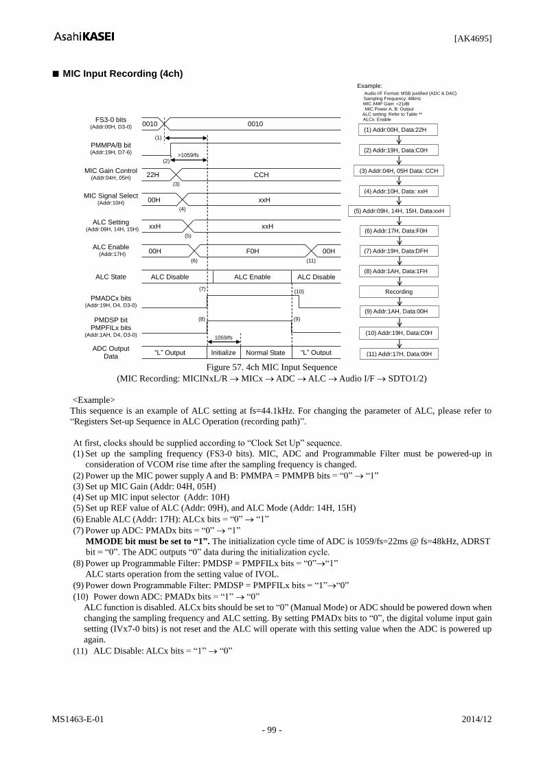
[AK4695]
MS1463-E-01 2014/12
- 99 -
MIC Input Recording (4ch)
(1)
FS3-0 bits (Addr:00H, D3-0) 0010
PMMPA/B bit (Addr:19H, D7-6)
0010
MIC Gain Control (Addr:04H, 05H)
PMADCx bits (Addr:19H, D4, D3-0)
PMDSP bit PMPFILx bits
(Addr:1AH, D4, D3-0)
ADC Output Data
“L” Output
(3)
(4)
(7)
(8)
1059/fs
Initialize
(9)
(10)
“L” Output Normal State
22H CCH
MIC Signal Select (Addr:10H) 00H xxH
ALC Setting (Addr:09H, 14H, 15H) xxH
(5)
xxH
ALC Enable (Addr:17H) 00H
(6)
F0H
ALC State ALC Disable ALC Disable ALC Enable
(2) >1059/fs
(11)
00H
Example: Audio I/F Format: MSB justified (ADC & DAC) Sampling Frequency: 48kHz MIC AMP Gain: +21dB MIC Power A, B: Output
ALC setting: Refer to Table ** ALCx: Enable
(3) Addr:04H, 05H Data: CCH
(1) Addr:00H, Data:22H
(5) Addr:09H, 14H, 15H, Data:xxH
(6) Addr:17H, Data:F0H
Recording
(9) Addr:1AH, Data:00H
(7) Addr:19H, Data:DFH
(11) Addr:17H, Data:00H
(8) Addr:1AH, Data:1FH
(10) Addr:19H, Data:C0H
(4) Addr:10H, Data: xxH
(2) Addr:19H, Data:C0H
Figure 57. 4ch MIC Input Sequence
(MIC Recording: MICINxL/R MICx ADC ALC Audio I/F SDTO1/2)
<Example>
This sequence is an example of ALC setting at fs=44.1kHz. For changing the parameter of ALC, please refer to
“Registers Set-up Sequence in ALC Operation (recording path)”.
At first, clocks should be supplied according to “Clock Set Up” sequence.
(1) Set up the sampling frequency (FS3-0 bits). MIC, ADC and Programmable Filter must be powered-up in
consideration of VCOM rise time after the sampling frequency is changed.
(2) Power up the MIC power supply A and B: PMMPA = PMMPB bits = “0” “1”
(3) Set up MIC Gain (Addr: 04H, 05H)
(4) Set up MIC input selector (Addr: 10H)
(5) Set up REF value of ALC (Addr: 09H), and ALC Mode (Addr: 14H, 15H)
(6) Enable ALC (Addr: 17H): ALCx bits = “0” “1”
(7) Power up ADC: PMADx bits = “0” “1”
MMODE bit must be set to “1”. The initialization cycle time of ADC is 1059/fs=22ms @ fs=48kHz, ADRST
bit = “0”. The ADC outputs “0” data during the initialization cycle.
(8) Power up Programmable Filter: PMDSP = PMPFILx bits = “0”“1”
ALC starts operation from the setting value of IVOL.
(9) Power down Programmable Filter: PMDSP = PMPFILx bits = “1”“0”
(10) Power down ADC: PMADx bits = “1” “0”
ALC function is disabled. ALCx bits should be set to “0” (Manual Mode) or ADC should be powered down when
changing the sampling frequency and ALC setting. By setting PMADx bits to “0”, the digital volume input gain
setting (IVx7-0 bits) is not reset and the ALC will operate with this setting value when the ADC is powered up
again.
(11) ALC Disable: ALCx bits = “1” “0”

[AK4695]
MS1463-E-01 2014/12
- 100 -
Stereo Line Input Recording
(1)
FS3-0 bits (Addr:00H, D3-0) 0010
PMMPA bit (Addr:19H, D6)
0010
MIC Gain Control (Addr:04H)
PMADC1-0 bits (Addr:19H, D1-0)
PMDSP bit PMPFIL1-0 bits
(Addr:1AH, D4, D1-0)
ADC Output Data
“L” Output
(2)
(3)
(4)
(5)
>1059/fs
Initialize
(7)
(8)
“L” Output Normal State
22H 22H
(6)
Input Signal Select (Addr:10H, D3-0) 0000 1010
Example:
Audio I/F Format: MSB justified Sampling Frequency: 48kHz MIC AMP Gain: +6dB
ALC: Off
(2) Addr:04H, Data: 22H
(1) Addr:00H, Data:22H
Recording
(7) Addr:1AH, Data:00H
(4) Addr:19H, Data:53H
(5) Addr:1AH, Data:13H
(8) Addr:19H, Data:00H
(6) Addr:19H, Data:13H
(3) Addr:10H, Data: 0AH
Figure 58. Stereo Line Input Recording Sequence
(Line Input Recording: AUXINL/R ADC1 Programmable Filter Audio I/F SDTO1)
<Example>
At first, clocks should be supplied according to “Clock Set Up” sequence.
(1) Set up a sampling frequency (FS3-0 bits). ADC and Programmable Filter must be powered-up in consideration of
VCOM rise time.
(2) Set up MIC gain (Addr: 04H)
(3) Set up MIC input selector (Addr: 10H)
(4) Power up ADC1 and MIC power supply A: PMMPA = PMAD1-0 bits = “0” “1”
MMODE bit must be set to “1”. The initialization cycle time of ADC is 1059/fs=22ms @ fs=48kHz, ADRST
bit = “0”. The ADC outputs “0” data during the initialization cycle.
(5) Power up Programmable Filter: PMDSP = PMPFIL1-0 bits = “0”“1”
(6) Power down MIC power supply A: PMMPA bit = “1” “0”
Power down the MIC power supply A after the initialization cycle of ADC1 (1059/fs) is finished.
(7) Power down Programmable Filter: PMDSP = PMPFIL1-0 bits = “1”“0”
(8) Power down ADC1: PMAD1-0 bits = “1” “0”

[AK4695]
MS1463-E-01 2014/12
- 101 -
Headphone-Amp Output
(1)
FS3-0 bits (Addr:00H, D3-0) XXXX
PMDACB bit (Addr:1BH, D1)
0010
DACAST bit (Addr:02H, D3)
DAC Path (Addr:12H)
PMHPL/R bits (Addr:1BH, D5-4)
HPL pin HPR pin
(2)
(3)
(4)
(5)
max. 26ms
(6)
DALB7-0 bits (Addr:0FH) 84H 70H
32H 12H
Example: Audio I/F Format: MSB justified Sampling Frequency: 48KHz
Digital Volume B: -10dB Programmable Filter, DRC: OFF
(1) Addr:00H, Data:22H
(3) Addr:0FH, Data:70H
(5) Addr:1BH, Data:12H
Playback
(4) Addr:12H, Data:12H
(6) Addr:1BH, Data:00H
(2) Addr:02H, Data:88H
Figure 59. Headphone-Amp Output Sequence
<Example>
At first, clocks should be supplied according to “Clock Set Up” sequence.
(1) Set up the sampling frequency (FS3-0 bits).
Headphone-Amp and DACB must be powered-up in consideration of VCOM rise up time.
(2) Set up the stabilization of Headphone-amp offset: DACAST bit = “0” “1”
(3) Set up the digital output volume B (Addr = 0FH)
(4) Set up the path of SDTI → DACB → Headphone-Amp: DASEL1-0 bits = “00”, DRCENB bit = “1” → “0”
(5) Power up DACB and Headphone-Amp: PMDACB = PMHPL = PMHPR bits = “0” → “1”
When PMHP bits= “1”, the charge pump circuit is powered-up. The power-up time of Headphone-Amp block is
26ms (max)
(6) Power down DACB and Headphone-Amp: PMDAC = PMHPL = PMHPR bits = “1” “0”

[AK4695]
MS1463-E-01 2014/12
- 102 -
Speaker-Amp Output
FS3-0 bits(Addr:00H, D3-0)
DVLB7-0 bits(Addr:0FH)
PMDRC bit(Addr:1AH, D7)
PMDACB bit
PMSPLO bit(Addr:1BH, D2-1)
0010xxxx
SPP pin Normal Output
SPPSN bit(Addr:02H, D2)
Hi-ZHi-Z
SPN pin Normal Output Hi-ZHi-Z SVDD/2 SVDD/2
(1)
xxH00H(5)
DAC Path(Addr:12H)
(6)
(7)
(10)
(8)
1100(2)
SPKG1-0 bits(Addr:03H, D6-)5
(4)
84H 70H(3)
32H 72H
DRC Control(Addr:31H-6EH)
DRC EnableDRC DisableDRC State DRC Disable
> 1 ms
(9)
Example:
Audio I/F Format: MSB justified Sampling Frequency:48KHz
Digital Volume B: -10dB DRC: Enable Programmable Filter OFF
(2) Addr:03H, Data:60H
(6) Addr:1AH, Data:80H Addr:1BH, Data:06H
(1) Addr:00H, Data:22H
(7) Addr:02H, Data:04H
(8) Addr:02H, Data:00H
Playback
(9) Addr:12H, Data:32H
(10) Addr:1AH, Data:00H Addr:1BH, Data:00H
(3) Addr:0FH, Data:70H
(5) Addr:31H-6EH, Data:xxH
(4) Addr:12H, Data:72H
Figure 60. Speaker-Amp Output Sequence
<Example>
At first, clocks must be supplied according to “Clock Set Up” sequence
(1) Set up the sampling frequency (FS3-0 bits). DAC and Speaker-Amp must be powered-up in consideration of
VCOM rise time.
(2) Set up SPK-Amp Gain: SPKG1-0 bits = “00” → “11”
(3) Set up Digital Output Volume B (Addr = 0FH)
(4) Set up the path of SDTI → DRC → DACB → SPK-Amp: DASEL1-0 bits = “00”, DACS bit = “0” → “1”,
DRCENB bit = “1”
(5) Set up DRC Control (Addr = 31H ~ 6EH)
(6) Power up DACB, DRC and SPK-Amp: PMDACB = PMDRC = PMSPLO bits = “0” → “1”
(7) Exit SPK-Amp power save mode: SPPSN bit = “0” → “1”
(8) Enter SPK-Amp power save mode: SPPSN bit = “1” → “0”
(9) Set up the path of SDTI → DRC → DACB → SPK-Amp: DACS bit = “1” → “0”
(10) Power down DAC, DRC and SPK-Amp: PMDACB = PMDRC = PMSPLO bits = “1” → “0”

[AK4695]
MS1463-E-01 2014/12
- 103 -
Stereo Line Output
FS3-0 bits(Addr:00H, D3-0)
DAC Path(Addr:12H)
PMDACA bit
PMLO bit(Addr:1BH, D3,D0)
0010xxxx
32H 22H
LOUTA pinROUTA pin
(1)
(4)
(5)
(2)
Normal Output
(7)
LOPSA bit(Addr:13H, D1)
(6) >300 ms
(8)
(9) >300 ms
(10)
84H 70H
LVOL bit(Addr:03H, D4)
0 1
DVLA7-0 bits(Addr:0EH)
(3)
Example:
Audio I/F Format: MSB justified (ADC & DAC) Sampling Frequency: 48kHz
Digital Volume B: 10dB
(1) Addr:00H, Data:22H
(2) Addr:03H, Data:10H
(4) Addr:12H, Data:22H
(5) Addr:13H, Data:02H
(6) Addr:1BH, Data:09H
Playback
(8) Addr:13H, Data:02H
(9) Addr:1BH, Data:00H
(10) Addr:09H, Data:00H
(3) Addr:0EH, Data:70H
(7) Addr:13H, Data:00H
Figure 61. Stereo Lineout Sequence
(Lineout Playback: SDTI DVLA DACA LOUTA/ROUTA)
<Example>
At first, clocks should be supplied according to “Clock Set Up” sequence.
(1) Set up the sampling frequency (FS3-0 bits). DAC and Stereo Line-Amp must be powered-up in consideration of
VCOM rise time.
(2) Set up Stereo Line-Amp A Volume: LVOL bit = “0” → “1”
(3) Set up Digital Output Volume A (Addr: 0EH)
(4) Set up the path of SDTI → DACA → Stereo Line-Amp A: DASEL1-0 bits = “00”, DRCENA bit = “0” → “1”
(5) Enter Stereo Line-Amp A power save mode: LOPSA bit = “0” → “1”
(6) Power up DAC and Stereo Line-Amp A: PMDACA = PMLO bits = “0” → “1”
When PMLO bit is set to “1”, LOUTA and ROUTA pins rise up to the VCOM voltage. The rise time is 300ms
(max.) when C=1F and AVDD=2.8V.
(7) Exit Stereo Line-Amp A power save mode: LOPSA bit = “1” → “0”
LOPSA bit should be set after LOUTA and ROUTA pins rise up. LPUTA and ROUTA pins start outputting
sound data after this setting.
(8) Enter Stereo Line-Amp A power save mode: LOPSA bit: “0” → “1”
(9) Power down DAC and Stereo Line-Amp A: PMDACA = PMLO bits = “1” → “0”
When PMLO bit is set to “0”, LOUTA and ROUTA pins fall down to the VSS voltage. The fall time is 300ms
(max.) when C=1F and AVDD=2.8V.
(10) Exit Stereo Line-Amp A power save mode: LOPSA bit = “1” → “0”
LOPSA bit should be set to “0” after LOUT and ROUT pins fall down.

[AK4695]
MS1463-E-01 2014/12
- 104 -
Stop of Clock
LRCK Input
(1)
BCKI Input
(1)
MCKI Input
(1)
Example
: Audio I/F Format:MSB justified(ADC & DAC) Input MCKI frequency:256fs Sampling Frequency:48kHz
(1) Stop the external clocks
Figure 62. Clock Stopping Sequence
<Example>
(1) Stop external clocks.
Power Down
Power supply current can be shut down (typ. 50μA) by stopping clocks and setting PMVCM bit = “0” after all blocks
except for VCOM are powered down. It can also be shut down (typ. 0A) by stopping clocks and setting the PDN pin = “L”.
When the PDN pin = “L”, all registers are initialized.

[AK4695]
MS1463-E-01 2014/12
- 105 -
PACKAGE
42-pin CSP
2.9
6 ±
0.0
3
B D C E F G
6
4
5
3
2
1
0.5
0.5
A
1
0.3
85 ±
0.0
16
0.2
38
± 0
.03
0.6
23 ±
0.0
36
C
42 x 0.317 ± 0.03
Bottom View Top View
(0.022) A
B 3.46 ± 0.03
A
0.03 C
0.015 M C A B
0.005 M C
(Unit: mm)
Material & Lead finish
Package material: Epoxy resin, Halogen (Br and Cl) free
Solder ball material: SnAgCu

[AK4695]
MS1463-E-01 2014/12
- 106 -
MARKING
4695 XXXX
A1
XXXX: Date code (4 digit)
Pin #A1 indication

[AK4695]
MS1463-E-01 2014/12
- 107 -
REVISION HISTORY
Date (Y/M/D) Revision Reason Page/Line Contents
12/12/05 00 First Edition
14/12/25 01 Spec Change 105 Package dimension was changed.
Top surface coating thickness: 0.025mm → 0.022mm
IMPORTANT NOTICE
0. Asahi Kasei Microdevices Corporation (“AKM”) reserves the right to make changes to the information
contained in this document without notice. When you consider any use or application of AKM product stipulated
in this document (“Product”), please make inquiries the sales office of AKM or authorized distributors as to
current status of the Products.
1. All information included in this document are provided only to illustrate the operation and application examples
of AKM Products. AKM neither makes warranties or representations with respect to the accuracy or
completeness of the information contained in this document nor grants any license to any intellectual property
rights or any other rights of AKM or any third party with respect to the information in this document. You are
fully responsible for use of such information contained in this document in your product design or applications.
AKM ASSUMES NO LIABILITY FOR ANY LOSSES INCURRED BY YOU OR THIRD PARTIES
ARISING FROM THE USE OF SUCH INFORMATION IN YOUR PRODUCT DESIGN OR
APPLICATIONS.
2. The Product is neither intended nor warranted for use in equipment or systems that require extraordinarily high
levels of quality and/or reliability and/or a malfunction or failure of which may cause loss of human life, bodily
injury, serious property damage or serious public impact, including but not limited to, equipment used in nuclear
facilities, equipment used in the aerospace industry, medical equipment, equipment used for automobiles, trains,
ships and other transportation, traffic signaling equipment, equipment used to control combustions or explosions,
safety devices, elevators and escalators, devices related to electric power, and equipment used in finance-related
fields. Do not use Product for the above use unless specifically agreed by AKM in writing.
3. Though AKM works continually to improve the Product’s quality and reliability, you are responsible for
complying with safety standards and for providing adequate designs and safeguards for your hardware, software
and systems which minimize risk and avoid situations in which a malfunction or failure of the Product could
cause loss of human life, bodily injury or damage to property, including data loss or corruption.
4. Do not use or otherwise make available the Product or related technology or any information contained in this
document for any military purposes, including without limitation, for the design, development, use, stockpiling
or manufacturing of nuclear, chemical, or biological weapons or missile technology products (mass destruction
weapons). When exporting the Products or related technology or any information contained in this document,
you should comply with the applicable export control laws and regulations and follow the procedures required
by such laws and regulations. The Products and related technology may not be used for or incorporated into any
products or systems whose manufacture, use, or sale is prohibited under any applicable domestic or foreign laws
or regulations.
5. Please contact AKM sales representative for details as to environmental matters such as the RoHS compatibility
of the Product. Please use the Product in compliance with all applicable laws and regulations that regulate the
inclusion or use of controlled substances, including without limitation, the EU RoHS Directive. AKM assumes
no liability for damages or losses occurring as a result of noncompliance with applicable laws and regulations.
6. Resale of the Product with provisions different from the statement and/or technical features set forth in this
document shall immediately void any warranty granted by AKM for the Product and shall not create or extend in
any manner whatsoever, any liability of AKM.
7. This document may not be reproduced or duplicated, in any form, in whole or in part, without prior written
consent of AKM.