2.4mhz pmic for battery powered system with i c controller
TRANSCRIPT

Copyright ANPEC Electronics Corp.Rev. A.3 - Apr., 2018
www.anpec.com.tw1
ANPEC reserves the right to make changes to improve reliability or manufacturability without notice, andadvise customers to obtain the latest version of relevant information to verify before placing orders.
2.4MHz PMIC for Battery Powered System with I2C Controller
APW7703A
Features
• Available in Linear Mode or Switch Mode Charge• High Efficiency 1.5A at Switch Mode Charge• Single Input USB-compliant/Adapter Charge - Input Voltage and Current Limit Supports USB2.
0 and USB3.0 - Programmable Input Current Limit : 100mA,
500mA, 900mA, 1300mA, 1700mA, 2100mA ,2500mA
• 3.9V-6V Input Operating Voltage Range - Support Input Voltage DPM Regulation• 1.5MHz Switching Frequency for Low Profile In-
ductor• Autonomous Battery Charging with or without
Host Management - Battery Charge Enable - Battery Charge Preconditioning - Charge Termination and Recharge• High Accuracy - +0.5% Charge Voltage Regulation - +7% Charge Current Regulation - +7.5% Input Current Regulation• Safety - Battery Precharge and Fast Charg Safety Timer - Thermal Shutdown - Input Over-Voltage Protection - MOSFET Over-Current Protection
• DSC/ DVR
• Action Camera
• Li-Ion battery powered devices
Simplified Application Circuit
Charger
Voltage Rail• Provide 4 Buck Single Phase PWM Converters - DC1: 0.6V - 1.5V at 4A Peak - DC2: 0.6V - 3.3V at 1.5A - DC3: 0.6V - 3.3V at 1A - DC4: 0.6V - 3.3V at 1.5A• Provide 3 LDO Output - RTCLDO 1.5V - 3.05V, 10mA - LDO1 0.6V - 3.3V, 150mA, Reference = 0.6V - LDO2 1.5V - 3.05V, 300mA, Controlled by I2C
• Provide 2 Load Switches Enable Signal• 30µA Low Battery Leakage Current• TQFN 5x5-40A Package• Lead Free and Green Devices Available (RoHS
Compliant)
Applications
LDO2
2.4MHzPWM
ConverterBuck1
Reference
I2CInterface
ThermalADC
2.4MHzPWM
ConverterBuck2
2.4MHzPWM
ConverterBuck3
2.4MHzPWM
ConverterBuck4
VLDO1
1.0V/150mALDO1
VLDO2
1.8V/300mA
RTCLDOVRTCLDO
1.95V/10mA
LS1
VLS1_EN
LS2
VLS2_EN
Linear or 1.5MHz
Switching Charger
DC11.0V/3A
DC43.0V/1.5ADC2
1.2V/1.5A
DC3
1.8V/1A
RNTC
VBYPASS

Copyright ANPEC Electronics Corp.Rev. A.3 - Apr., 2018
www.anpec.com.tw2
APW7703A
Ordering and Marking Information
Note: ANPEC lead-free products contain molding compounds/die attach materials and 100% matte tin plate termination finish; whichare fully compliant with RoHS and compatible with both SnPb and lead-free soldiering operations. ANPEC lead-free products meet orexceed the leadfree requirements of IPC/JEDEC J STD-020C for MSL classification at lead-free peak reflow temperature.
General DescriptionThe APW7703A is a Power Management IC (PMIC) with a battery powered system designed to provide completePower Management solution for the camera applications. The IC operates from a single supply voltage of 2.7V to 5.5V allowing it to be used in Adapter/USB or 1 Cell battery applications. The APW7703A is designed to providemaximum number of regulators in the smallest available cost effective package. Included in the IC are: One select-able linear mode or switch mode charger; Four switching Buck converters for DC1/DC2/DC3/DC4, Three LDOs forImage Signal Process and RTC applications, and Two Load Switch Enable Signal Control for Wi-Fi, DRAM applications.For Charger part, when the input current limit or voltage limit is reached, the power path management automaticallyreduces the charge current to zero. As the system load continues to increase, the power path discharges the batteryuntil the system power requirement is met. This supplement mode operation prevents overloading the input source.The devices initiate and complete a charging cycle without software control. It automatically detects the battery voltageand charges the battery in three phases: pre-conditioning, constant current and constant voltage. At the end of thecharging cycle, the charger automatically terminates when the charge current is below a preset limit in the constantvoltage phase. When the full battery falls below the recharge threshold, the charger will automatically start anothercharging cycle.The device provides various safety features for battery charging operation, including a pack negative thermistormonitoring, charging safety timer and over-voltage/over-current protections.For the other VRs, the IC is equipped with all the standard protection features such as current limit, over voltage andinternal under voltage lock out protection as well as thermal shutdown.The serial interface is an I2C communication interface which allows supply sequencing as well as controlled margin-ing of ramp up and ramp down of all supplies to optimize battery power consumption. The I2C interface also allows foradjustability of VRs’ voltage and Forced PWM Mode in default operation and Auto PSM/PWM Mode in OFF mode state.Also, the power sequenc is defined by strobes and delay times under I2C Control.The device is available in a 40-pin, 5x5 mm2 thin QFN package for best thermal performance while optimizing the cost.
APW7703A Package Code QB: TQFN5x5-40AOperating Ambient Temperature Range
I : -40 to 85oCHandling Code
TR : Tape & ReelAssembly Material
Handling Code
Temperature Range
Package Code G : Halogen and Lead Free Device
Assembly Material
APW7703A QB : APW7703AXXXXX XXXXX - Date Code

Copyright ANPEC Electronics Corp.Rev. A.3 - Apr., 2018
www.anpec.com.tw3
APW7703A
Pin Configuration
Symbol Parameter Rating Unit
VVBUS VBUS to GND Voltage -0.3 ~ 20 V
VVSYS VSYS to GND Voltage -0.3 ~ 6.5 V
VIN_DC1, VIN_DC2, VIN_DC3, VIN_DC4, VINLDO1, VINLDO2, LS1_EN, LS2_EN to GND Vol tage -0.3 ~ 6.5 V
LX_DC1, LX_DC2, LX_DC3, LX_DC4 to GND Voltage -0.3 ~ 6.5 V
FB_DC1, FB_DC2, FB_DC3, FB_DC4, RTCLDO, LDO1, LDO2, FB_LDO1 to GND Voltage -0.3 ~ 6.5 V
All other pins to GND Voltage -0.3 ~ 6.5 V
PGND to AGND -0.3 ~ 0.3 V
TJ Maxim um Junction Temperature -40 ~ 150 oC
TSTG Storage Temperature -65 ~ 150 oC
TSDR Maxim um Lead So ldering Temperature (10 Seconds) 260 oC
Absolute Maximum Ratings (Note 1)
Note1: Stresses beyond those listed under "absolute maximum ratings" may cause permanent damage to the device. These arestress ratings only and functional operation of the device at these or any other conditions beyond those indicated under "recom-mended operating conditions" is not implied. Exposure to absolute maximum rating conditions for extended periods may affect devicereliability
Thermal CharacteristicsSymbol Parameter Typical Value Unit
θJA Junction- to-Ambient Resistance in free air (Note 2) 30 oC/W
Note 2: θJA is measured with the component mounted on a high effective thermal conductivity test board in free air. The exposed padof TQFN5x5-40A is soldered directly on the PCB.
Exposed Pad(PGND)
WAK
EUP1
WAK
EUP0 TS
1 2 3 4 5 6 7 8 9 1011
12
13
14
15
16
17
18
19
2021222324252627282930
31
32
33
34
35
36
37
38
39
40VB
AT(C
SN
)
CS
P
BGA
TE
WAK
EUP2
VSY
S
CH
GO
UT
VSY
S
VBUS
VBUS
FB_DC2
VIN_DC4
VIN_DC2
LX_DC2
LS1_EN
LX_DC4
FB_DC4
LS2_EN
FB_L
DO
1
LX_D
C1
SCL
SDA
VIN
LDO
1
PGN
D
VIN
LDO
2
VIN
_DC
1
LX_D
C3
FB_D
C1
LDO
2
LDO
1
FB_DC3
VIN_DC3
RTCLDO
BYPASS
AGND
CHG_STAT
PGOOD
/INT

Copyright ANPEC Electronics Corp.Rev. A.3 - Apr., 2018
www.anpec.com.tw4
APW7703A
Recommended Operating Conditions (Note 3)
Symbol Parameter Range Unit
VVBUS USB/Adapter Input Voltage 3.9~5.5 V
VVBAT Battery Voltage 2.7~4.4 V
VDC1 Buck1 Output Voltage 0.6~1.5 V
IDC1 Buck1Output Current ~2.5 A
VDC2 Buck2 Output Voltage 0.6~3.3 V
IDC2 Buck2 Output Current ~1.5 A
VDC3 Buck3 Output Voltage 0.6~3.3 V
IDC3 Buck3 Output Current ~1 A
VDC4 Buck4 Output Voltage 0.6~3.3 V
IDC4 Buck4 Output Current ~1.5 A
VRTCLDO RTCLDO Output Voltage 1.5 ~ 3.05 V
IRTCLDO RTCLDO Output Current ~10 mA
VLDO1 LDO1 Output Voltage 0.6~3.3 V
ILDO1 LDO1 Output Current ~150 mA
VLDO2 LDO2 Output Voltage 1.5~3.3 V
ILDO2 LDO2 Output Current ~300 mA
TA Ambient Temperature -40 ~ 85 oC
TJ Junction Temperature -40 ~ 125 oC
Note 3 : Refer to the typical application circuit.

Copyright ANPEC Electronics Corp.Rev. A.3 - Apr., 2018
www.anpec.com.tw5
APW7703A
Electrical CharacteristicsUnless otherwise specified, these specifications apply over VVBUS_UVLO<VVBUS<VACOV and VVBUS>VBAT+VSLEEPZ, and TA= -40to 85 oC. Typical values are at TA=25oC.
APW7703A Symbol Parameter Test Conditions
Min Typ Max Unit
QUIESCENT CURRENTS
IBAT Battery Supply Current (BAT, CHGOUT, SYS)
Al l other rails disabled, No VBUS, BGATE Enabled, VBAT= 4.2V - 32 55 μA
VBUS=5V, A ll other rails disabled, No Battery, RTCLDO enabled, No Load, TA=-40~85
- 600 - μA
IVBUS Input Supply Current (VBUS) VBAT > VBATUVLO, VBUS - VBAT > VSLEEPZ
(VBUS=5V, VBAT=4.2V), Charge converter not swi tching , A ll other rails d isabled
- 4.5 6 mA
VBUS/BAT POWER UP, POWER POR
VBUS USB Input Vo ltage Range Valid range for charging 3.9 - 6 V
VBUS_POR USB Valid VBUS Rising 3.4 3.6 3.8 V
VBUS_POR_HYS USB Valid Hysteresis VBUS Fall ing - 200 - mV USB is connected 0 - 5.5 V
VBAT Battery Input Voltage Range USB is not connected 2.7 - 5.5 V
VSLEEP Sleep Mode Falling Threshold VVBUS falling, VVBUS-VBAT (Into Sleep Mode) 35 80 120 mV
VSLEEPZ Sleep Mode Rising Threshold VVBUS rising, VVBUS-VBAT (Out of Sleep Mode) 170 250 300 mV
VSYS_POR_R VSYS UVLO Voltage Thresho ld VSYS Rising 2.9 3.0 3.1 V
VSYS_POR_F VSYS UVLO Voltage Thresho ld VSYS Falling 2.7 2.8 2.9 V
VSYS_POR_HYS VSYS UVLO Voltage Hysteresis - 0.2 - V
VACOV USB Over Voltage Rising Threshold VBUS rising 6.2 6.4 6.6 V
VACOV_HYS USB Over Voltage Falling Hysteresis VBUS falling - 200 - mV
POWER PATH MANAGEM ENT`
RON(RBFET) In ternal Top Reverse Blocking MOSFET On-Resistance Between VBUS and VSYS
Measured between VBUS and SYS, VBUS=5V, ISYS=1A
- 100 - mΩ
RON(HSET)
In ternal High Side MOSFET On-Resistance Between VSYS and CHGOUT
Measured between HS D-S Terminal volage, VBUS=5V, IHS_DS=1A - 50 - mΩ
VSYS_BAT SYS/BAT Com parator VBAT -VSYS, VSYS Faling - 30 - mV
BYPASS LDO
VVBUS=5V, IBYPASS=0mA - 4 - V VBYPASS BYPASS Output Vo ltage
VVBUS=5V, IBYPASS=20mA 3 - 4.5 V
IBYPASS BYPASS Output Current VVBUS=5V, BYPASS Shortr to GND - 40 - mA
BATTERY CHARGER
VOREG_ACC_SW VBAT= 4.208V, TA= 25°C, Switch Mode -0.5 - 0.5 %
VOREG_ACC_LR Charge Vol tage Regulation Accuracy
VBAT= 4.208V, TA= 25°C, Linear Mode -1 - 1 %
Charge Vol tage Regulation Range I2C selectab le; Default: 4 .208V 3.504 - 4.464 V
• Charger

Copyright ANPEC Electronics Corp.Rev. A.3 - Apr., 2018
www.anpec.com.tw6
APW7703A
Electrical Characteristics (Cont.)
APW7703A Symbol Parameter Test Conditions
Min Typ Max Unit
BATTERY CHARGER (Cont.)
VBAT= 3.8V, ICHG= 1024mA, TA= 25°C -7 - 7
VBAT= 3.8V, ICHG= 512mA , TA= 25°C -10 - 10 ICHG_REG_ACC_SW Switch Mode Fast Charge Current Regulation Accuracy
VBAT= 3.8V, ICHG= 128mA , TA= 25°C -20 - 20
%
VBAT= 3.8V, ICHG= 640mA, TA= 25°C -10 10
VBAT= 3.8V, ICHG= 440mA , TA= 25°C -12 12
VBAT= 3.8V, ICHG= 255mA , TA= 25°C -15 15 ICHG_REG_ACC_LR Linear Mode Fast Charge Current
Regulation Accuracy
VBAT= 3.8V, ICHG= 100mA , TA= 25°C -25 25
%
ICHG[2:0]=000 - 128 -
ICHG[2:0]=001 - 256 -
ICHG[2:0]=010 - 384 -
ICHG[2:0]=011 512
ICHG[2:0]=100 - 640 -
ICHG[2:0]=101 - 768 -
ICHG[2:0]=110 - 896 -
ICHG_SW Switch Mode, RSNS= 100mΩ, Battery Fast Chage Current Range, VOREG > VBAT > VLOWV, VBUS= 5V
ICHG[2:0]=111 - 1024 -
mA
ICHG[2:0]=000 - 100 -
ICHG[2:0]=001 - 255 -
ICHG[2:0]=010 - 440 - ICHG_LR
Linear Mode, Battery Fast Chage Current Range, VOREG > VBAT > VLOWV, VBUS= 5V
ICHG[2:0]=011 640
mA
VBATLOWV_F Battery LOWV Falling Thresho ld Fast charge to precharge, VBUS=5V, VPRECHG= 0 2.4 2.6 2 .8 V
VBATLOWV_R Battery LOWV Rising Threshold Precharge to fast charge, VBUS=5V, VPRECHG= 0
2.6 2.8 3 .0 V
IPRECHG_ACC_SW Switch Mode Precharge Current Regulation Accuracy VBAT= 2.6V, IPRECHG= 128mA, TA= 25°C -20 - 20 %
IPRECHG_ACC_LR Linear Mode Precharge Current Regulation Accuracy VBAT= 2.6V, IPRECHG= 100mA, TA= 25°C -25 - 25 %
IPRECHG[1:0]=00 - 64 -
IPRECHG[1:0]=01 - 128 -
IPRECHG[1:0]=10 - 192 -
Switch Mode, RSNS=100mΩ, Battery Precharge Chage Current Range, VBAT < VLOWV, VVBUS=5V
IPRECHG[1:0]=11 - 256 -
mA
IPRECHG[1:0]=00 - 50 -
IPRECHG[1:0]=01 - 100 -
IPRECHG[1:0]=10 - 180 -
Linear Mode, Battery Precharge Chage Current Range, VBAT < VLOWV, VVBUS=5V
IPRECHG[1:0]=11 - 255 -
mA
ITERM_ACC Linear/Swi tch Mode Termination Current Regulation Accuracy ITERM=256mA, ICHG=1024mA, TA= 25°C -22.5 - 22.5 %
Unless otherwise specified, these specifications apply over VVBUS_UVLO<VVBUS<VACOV and VVBUS>VBAT+VSLEEPZ, and TA= -40to 85 oC. Typical values are at TA=25oC.

Copyright ANPEC Electronics Corp.Rev. A.3 - Apr., 2018
www.anpec.com.tw7
APW7703A
Electrical Characteristics (Cont.)
APW 7703A Symbol Parameter Test Conditions
Min Typ M ax Unit
BATTERY CHARGER (Cont.)
ITERM[1:0]=00 - 64 -
ITERM[1:0]=01 - 128 -
ITERM[1:0]=10 - 192 -
L inear Mode, or Switch Mode, RSNS=100mΩ , Charge Current Value for Termination Detection Threshold
ITERM[1:0]=11 - 256 -
mA
Termination Deglitch Time - 125 - ms
VBAT_SHORT Battery Short Voltage VBAT falling (into Battery Short State) - 2 - V
VBAT_SHORT_HYS Battery Short Voltage Hysteresis VBAT rising (Out o f Battery Short State) - 200 - mV
ISHORT Battery Short Current VBAT < 2.0V ( In Battery Short State) - 32 - mA
VRECHG Recharge Threshold Below VBAT_REG VBAT falling, After Charge Termination, VBAT=4.208V
70 100 150 mV
tRECHG Recharge Deglitch Time VBAT falling - 125 - ms
INPUT VOLTAGE/CURRENT REGULATION
VINDPM_ACC Input Voltage Regulation Accuracy VINDPM = 4.5V (Default) -2 - 2 %
Threshold at which DPM Loop Enabled I2C Selectable 4 .4 - 4.7 V
IVBUS [2:0]=000 50 - 150 mA
IVBUS [2:0]=001 400 - 600 mA
IVBUS [2:0]=010 750 - 900 mA
IVBUS [2:0]=011 1080 - 1300 mA
IVBUS [2:0]=100 1410 - 1700 mA
IVBUS [2:0]=101 1740 - 2100 mA
Input Current Limit
IVBUS [2:0]=110 2000 - 2500 mA
BATTERY OVER-VOLTAGE PROTECTION
VBATOVP Battery Over-Vo ltage Threshold VBAT rising, as percentage o f VBAT_REG, VBAT= 4.208V - 106 - %
VBATOVP_HYS Battery Over-Vo ltage Hysteresis VBAT fall ing, as percentage of VBAT_REG, VBAT= 4.208V - 3 - %
tBATOVP Battery Over-Vol tage Deglitch Time To Disable Charge - 1 - μs
BATTERY NTC MONITOR Pull-up resistor from thermistor to bypass NTC= 10k (β=3380) - 10 - kΩ
RNTC_PU Accuracy TA= 25°C -3 - 3 %
Temperature falling - 73.9 - VLTH Low temp failure threshold
Temperature rising TRANGE= 0/1 (0°C)
- 72.1 - %
Temperature falling - 34.4 -
Temperature rising TRANGE= 0 (45°C)
- 32.9 -
Temperature falling - 24.4 - VHTH High temp failure threshold
Temperature rising TRANGE= 1 (60°C)
- 23.3 -
%
Unless otherwise specified, these specifications apply over VVBUS_UVLO<VVBUS<VACOV and VVBUS>VBAT+VSLEEPZ, and TA= -40 to 85 oC.Typical values are at TA=25oC.

Copyright ANPEC Electronics Corp.Rev. A.3 - Apr., 2018
www.anpec.com.tw8
APW7703A
Electrical Characteristics (Cont.)
APW 7703A Symbol Parameter Test Conditions
Min Typ Max Unit
BATTERY NTC MONITOR (Cont.)
Temperature falling - 27.4 -
Temperature r ising TRANGE= 0 (55°C)
- 26.2 -
Temperature falling - 19.3 - VDIS Discharge temperature threshold
Temperature r ising TRANGE= 1 (70°C)
- 18.4 -
%
TDET Thermistor Detect Degritch Time - 10 - ms
THERM AL SHUTDOWN
TSHUT Thermal Shutdown Rising Temperature Temperature increasing - 160 - °C
TSHUT_HYS Thermal Shutdown Hysteresis - 30 - °C
OVER TEMPERATURE AUTO- DISCHARGE CIRCUIT
VDISCH_ON Discharge turn-on threshold Voltage Turn on discharging at h igh temp if battery voltage is above (DIS_EN= 1) - 3.9 - V
Discharge hysteresis when VBAT Drops; I2C Selectable ; DISOFF=1 - 0.1 - V
VDISCH_HYS Discharge Hysteresis Discharge hysteresis when VBAT Drops; I2C Selectable ; DISOFF=0 - 0.2 - V
Battery temp above discharge threshold ((VTS≦VDIS) ), RDIS=0 56 80 104 Ω
RDISCH Automatic discharge resistor Battery temp above discharge threshold ((VTS≦VDIS) ), RDIS=1 140 200 260 Ω
CHARGE OVER-CURRENT COMPARATOR
IHSFET_OCP HSFET Over-Current Threshold 3 4 - A
PWM OPERATION
FSW PW M Switching Frequency 1.3 1.5 1.7 MHz
PW M Switching Frequency Accuracy -40 ~ 85°C -10 - 10 %
ICHGOUT_LEAK CHGOUT Leakage Current VSYS=VCHGOUT=5V, Charger is disable - - 1 μA
I/O PIN CHARACTERISTICS (SDA, SCL, /INT, ADD_SEL, CSN, CSP, WAKEUP0, WAKEUP1, WAKEUP2, PGOOD)
VIL Input Low Voltage Include SDA, SCL, /INT, WAKEUP0, WAKEUP1, WAKEUP2 Input Pins - - 0.4 V
V IH Input High Voltage Include SDA, SCL, /INT, WAKEUP0, WAKEUP1, WAKEUP2 Input Pins 1.5 - - V
VO_LOW Output Low Saturation Voltage Sink current=5mA Include PGOOD, /INT Pins - - 0.4 V
Pull up to 5V, Include SDA, SCL Input Pins - - 1 μA Pull up to 5V, Include WAKEUP0, WAKEUP1, WAKEUP2 Input Pins - 50 - μA IBIAS_IO High Level Leakage Current Pull up to 5V, Include PGOOD and /INT Input P ins - - 0.2 μA
TINT_L /INT Pulled Low Time /INT Pu lled Low Time When Fault Event still Exists. The Period is 1ms - 10 - μs
fSCL SCL Clock Frequency - - 400 kHz
Unless otherwise specified, these specifications apply over VVBUS_UVLO<VVBUS<VACOV and VVBUS>VBAT+VSLEEPZ, and TA= -40 to 85 oC.Typical values are at TA=25oC.

Copyright ANPEC Electronics Corp.Rev. A.3 - Apr., 2018
www.anpec.com.tw9
APW7703A
Electrical Characteristics (Cont.)
APW 7703A Symbol Parameter Test Conditions
Min Typ M ax Unit
PGOOD Definition (Relative with all DC/DC Converters, Load Switch and LDOs )
PGOOD Delay Time Defaul t, All VRs are regulated - 64 - ms
WAKEUP0 Hard Reset Detect Time RSTTMR_EN =0 - 16 - sec
VBUS POR OKAY to Wakupx Enable Delay Time - 150 - μs
VBUS POR OKAY to VR Starts to Rise Up Delay Time
From Wakeupx Has Enabled First to DC1 Starts to Rise Up Period, No Battery - 50 - ms
WAKEUP0/1/2 Deglitch Time Minim um WAKEUPx Pulsed W idth 500 - - μs
Timing Requirement
PCHRGT=0 - 30 - min
Precharge Timer, Thermal and DPM Loop Not Active. Selectable by I2C PCHRGT=1 - 60 - min
Charge Safety Timer, Thermal and DPM Loop Not Active. Selectable by I2C
4 - 10 hr
Unless otherwise specified, these specifications apply over VVBUS_UVLO<VVBUS<VACOV and VVBUS>VBAT+VSLEEPZ, and TA= -40 to 85 oC.Typical values are at TA=25oC.
Copyright ANPEC Electronics Corp.Rev. A.3 - Apr., 2018
www.anpec.com.tw10
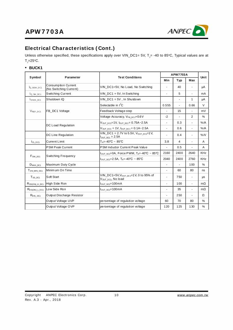
APW7703A
Electrical Characteristics (Cont.)
APW7703A Symbol Parameter Test Conditions
Min Typ Max Unit
IQ_NSW_DC1 Consumption Current (No Switching Current) VIN_DC1=5V, No Load, No Switching - 40 - μA
IQ_SW_DC1 Switching Current VIN_DC1 = 5V, In Swi tching - 5 - mA
ISHUN_DC1 Shutdown IQ VIN_DC1 = 5V , In Shutdown - 1 μA
Selectable in I2C 0.555 - 0.66 V
Feedback Vol tage step - 15 - mV VREF_DC1 FB_DC1 Voltage
Voltage Accuracy, VFB_DC1=0.6V -2 - 2 %
VOUT_DC1=1V, IOUT_DC1= 0.75A~2.5A - 0.3 - %/A DC Load Regulation
VOUT_DC1 = 1V, IOUT_DC1 = 0.1A~2.5A - 0.6 - %/A
DC Line Regulation VIN_DC1 = 2.7V to 5.5V, VOUT_DC1=1V, IOUT_DC1 = 2.5A - 0.4 - %/V
ICL_DC1 Current L imit TA=-40 ~ 85 3.8 4 - A
PSM Peak Current PSM Inductor Current Peak Value - 0.5 - A
IOUT_DC1=0A, Force PWM, TA=-40 ~ 85 2160 2400 2640 KHz FSW_DC1 Switching Frequency
IOUT_DC1=2.5A, TA=-40 ~ 85 2040 2400 2760 KHz
DMAX_DC1 Maximum Duty Cycle - - 100 %
TON_MIN_DC1 Minim um On Time - 60 80 ns
TSS_DC1 Soft Start VIN_DC1=5V,VOUT_DC1=1V, 0 to 95% of VOUT_DC1, No load - 750 - μs
RDS(ON)_H_DC1 High S ide Ron IOUT_DC1=100mA - 100 - mΩ
RDS(ON)_L_DC1 Low Side Ron IOUT_DC1=100mA - 35 - mΩ
RDIS_DC1 Output Discharge Resistor - 250 - Ω
Output Voltage UVP persentage of regula tion vo ltage 60 70 80 %
Output Voltage OVP persentage of regula tion vo ltage 120 125 130 %
Unless otherwise specified, these specifications apply over VIN_DC1= 5V, TJ= -40 to 85oC, Typical values are atTJ=25oC.
• BUCK1

Copyright ANPEC Electronics Corp.Rev. A.3 - Apr., 2018
www.anpec.com.tw11
APW7703A
Electrical Characteristics (Cont.)
APW7703A Symbol Parameter Test Conditions
Min Typ Max Unit
IQ_NSW_DC2 Consumption Current (No Switching Current) VIN_DC2=5V, No Load, No Switching - 40 - μA
I Q_SW_DC2 Switching Current VIN_DC2 = 5V, In Swi tching - 5 - mA
ISHUN_DC2 Shutdown IQ VIN_DC2 = 5V , In Shutdown - 1 μA
Selectable in I2C 0.555 - 0.66 V
Feedback Vol tage step - 15 - mV VREF_DC2 FB_DC2 Voltage
Voltage Accuracy, VFB_DC2=0.6V -2 - 2 %
VOUT_DC2=1.2V, IOUT_DC2= 0.5A~1.5A - 0.3 - %/A DC Load Regulation
VOUT_DC2 = 1.2V, IOUT_DC2=0.1A~1.5A - 0.6 - %/A
DC Line Regulation VIN_DC2=2.7V to 5.5V, VOUT_DC2=1.2V, IOUT_DC2=1.5A
- 0.4 - %/V
ICL_DC2 Current L imit TA=-40 ~ 85 2.2 3 - A
PSM Peak Current PSM Inductor Current Peak Value - 0.5 - A
IOUT_DC2=0A, Force PWM, TA=-40 ~ 85 2160 2400 2640 KHz FSW_DC2 Switching Frequency
IOUT_DC2=1.5A, TA=-40 ~ 85 2040 2400 2760 KHz
DMAX_DC2 Maximum Duty Cycle - - 100 %
TON_MIN_DC2 Minim um On Time - 60 80 ns
TSS_DC2 Soft Start VOUT_DC2=1.2V, 0 to 95% of VOUT_DC2, No load - 750 - μs
RDS(ON)_H_DC2 High S ide Ron
IOUT_DC2=100mA - 130 - mΩ
RDS(ON)_L_DC2 Low Side Ron IOUT_DC2=100mA - 65 - mΩ
RDIS_DC2 Output Discharge Resistor - 250 - Ω
Output Voltage UVP persentage of regula tion vo ltage 60 70 80 %
Output Voltage OVP persentage of regula tion vo ltage 120 125 130 %
Unless otherwise specified, these specifications apply over VIN_DC2= 5V, TJ= -40 to 85oC, Typical values are atTJ=25oC.
• BUCK2
Copyright ANPEC Electronics Corp.Rev. A.3 - Apr., 2018
www.anpec.com.tw12
APW7703A
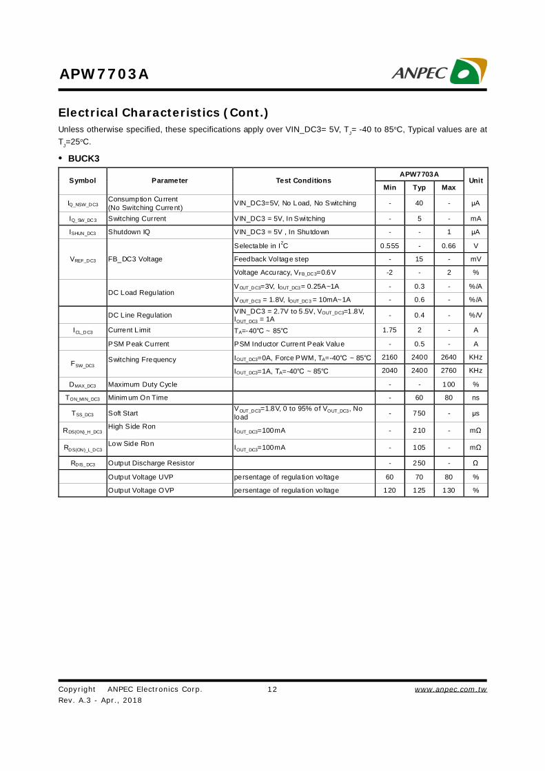
Electrical Characteristics (Cont.)
APW7703A Symbol Parameter Test Conditions
Min Typ Max Unit
IQ_NSW_DC3 Consumption Current (No Switching Current) VIN_DC3=5V, No Load, No Switching - 40 - μA
IQ_SW_DC3 Switching Current VIN_DC3 = 5V, In Swi tching - 5 - mA
ISHUN_DC3 Shutdown IQ VIN_DC3 = 5V , In Shutdown - - 1 μA
Selectable in I2C 0.555 - 0.66 V
Feedback Vol tage step - 15 - mV VREF_DC3 FB_DC3 Voltage
Voltage Accuracy, VFB_DC3=0.6V -2 - 2 %
VOUT_DC3=3V, IOUT_DC3= 0.25A~1A - 0.3 - %/A DC Load Regulation
VOUT_DC3 = 1.8V, IOUT_DC3 = 10mA~1A - 0.6 - %/A
DC Line Regulation VIN_DC3 = 2.7V to 5.5V, VOUT_DC3=1.8V, IOUT_DC3 = 1A - 0.4 - %/V
ICL_DC3 Current L imit TA=-40 ~ 85 1.75 2 - A
PSM Peak Current PSM Inductor Current Peak Value - 0.5 - A
IOUT_DC3=0A, Force PWM, TA=-40 ~ 85 2160 2400 2640 KHz FSW_DC3 Switching Frequency
IOUT_DC3=1A, TA=-40 ~ 85 2040 2400 2760 KHz
DMAX_DC3 Maximum Duty Cycle - - 100 %
TON_MIN_DC3 Minim um On Time - 60 80 ns
TSS_DC3 Soft Start VOUT_DC3=1.8V, 0 to 95% of VOUT_DC3, No load - 750 - μs
RDS(ON)_H_DC3 High S ide Ron IOUT_DC3=100mA - 210 - mΩ
RDS(ON)_L_DC3 Low Side Ron
IOUT_DC3=100mA - 105 - mΩ
RDIS_DC3 Output Discharge Resistor - 250 - Ω
Output Voltage UVP persentage of regula tion vo ltage 60 70 80 %
Output Voltage OVP persentage of regula tion vo ltage 120 125 130 %
Unless otherwise specified, these specifications apply over VIN_DC3= 5V, TJ= -40 to 85oC, Typical values are atTJ=25oC.
• BUCK3

Copyright ANPEC Electronics Corp.Rev. A.3 - Apr., 2018
www.anpec.com.tw13
APW7703A
Electrical Characteristics (Cont.)
APW7703A Symbol Parameter Test Conditions
Min Typ Max Unit
IQ_NSW_DC4 Consumption Current (No Switching Current) VIN_DC4=5V, No Load, No Switching - 40 - μA
IQ_SW_DC4 Switching Current VIN_DC4 = 5V, In Swi tching - 5 - mA
ISHUN_DC4 Shutdown IQ VIN_DC4 = 5V , In Shutdown - 1 μA
Selectable in I2C 0.555 - 0.66 V
Feedback Vol tage step - 15 - mV VREF_DC4 FB_DC4 Voltage
Voltage Accuracy, VFB_DC4=0.6V -2 - 2 %
VOUT_DC4=3V, IOUT_DC4= 0.5A~1.5A - 0.3 - %/A DC Load Regulation
VOUT_DC4 = 3V, IOUT_DC4 = 0.1A~1.5A - 0.6 - %/A
DC Line Regulation VIN_DC4 = 2.7V to 5.5V, VOUT_DC4=3V, IOUT_DC4 = 1 .5A - 0.4 - %/V
ICL_DC4 Current L imit TA=-40 ~ 85 2.2 3 - A
PSM Peak Current PSM Inductor Current Peak Value - 0.5 - A VIN_DC4=2.7V to 5.5V, IOUT_DC4=0A, Force PW M, TA=-40 ~ 85 2160 2400 2640 KHz
FSW_DC4 Switching Frequency VIN_DC4=2.7V to 5.5V, IOUT_DC4=1.5A,
TA=-40 ~ 85 2040 2400 2760 KHz
DMAX_DC4 Maximum Duty Cycle - - 100 %
TON_MIN_DC4 Minim um On Time - 60 80 ns
TSS_DC4 Soft Start VIN=5V,VOUT_DC4=3V, 0 to 95% of VOUT_DC4, No load - 750 - μs
RDS(ON)_H_DC4 High S ide Ron VIN_DC4=2.7V, IOUT_DC4=100mA - 130 - mΩ
RDS(ON)_L_DC4 Low Side Ron VIN_DC4=2.7V, IOUT_DC4=100mA - 65 - mΩ
RDIS_DC4 Output Discharge Resistor - 250 - Ω
Output Voltage UVP persentage of regula tion vo ltage 60 70 80 %
Output Voltage OVP persentage of regula tion vo ltage 120 125 130 %
Unless otherwise specified, these specifications apply over VIN_DC4= 5V, TJ= -40 to 85oC, Typical values are atTJ=25oC.
• BUCK4

Copyright ANPEC Electronics Corp.Rev. A.3 - Apr., 2018
www.anpec.com.tw14
APW7703A
Electrical Characteristics (Cont.)
APW7703A Symbol Parameter Test Conditions
Min Typ Max Unit
RTCLDO Output Vo ltage Adjustable by I2C 1.5 - 3.05 V
IRTCLDO_Max RTCLDO Source Capability V VIN_RTCLDO=3.7V, VOUT_RTCLDO =1.95V - - 10 mA
DC Output Voltage Accuracy IOUT_RTCLDO=10mA, V VIN_RTCLDO> VOUT_RTCLDO+150mV, VOUT_RTCLDO=1.95V -3 - 3 %
Load Regula tion IOUT_RTCLDO=0mA~10mA, V VIN_RTCLDO=3.7V, VOUT_RTCLDO =1.95V
-3 - 3 %
Line Regulation
V VIN_RTCLDO=3.7V~5V, IOUT_RTCLDO=10mA, VOUT_RTCLDO=1.95V -3 - 3 %
IOUT_RTCLDO=10mA, VOUT_RTCLDO=1.95V, TA=25 - 150 200 mV
VDROPOUT_RTC VSYS-VOUT_RTCLDO Dropout Voltage
TJ= -40 ~125 - 200 265 mV
ICL_RTC Short Circui t Current Limit VOUT_RTCLOD1 Short to GND, V VIN_RTCLDO=5V - 150 - mA
RDS(ON)_RTC R_LDORTC - 10 - Ω
Unless otherwise specified, these specifications apply over VSYS= 5V, TJ= -40 to 85oC, Typical values are at TJ=25oC.
• RTCLDO

Copyright ANPEC Electronics Corp.Rev. A.3 - Apr., 2018
www.anpec.com.tw15
APW7703A
Electrical Characteristics (Cont.)
APW7703A Symbol Parameter Test Conditions
Min Typ Max Unit
LDO1 Output Vo ltage Range Output Adjustable, VFB_LDO1=0.6V 0.6 - 3.3 V
DC Output Voltage Accuracy ILDO1=10mA, VVINLDO1 > VLDO1+30mV, -2 - 2 %
Load Regula tion ILDO1=0mA to 150mA, VVINLDO1=1.8V, VLDO1 =1.0V -1.5 - 1.5 %
Line Regulation
VVINLDO1=1.8V to 5V, ILDO1=150mA, VLDO1=1.0V -1.5 - 1.5 %
VINLDO1 POR Voltage Threshold VINLDO1 Rising 0.9 1 1.1 V
VINLDO1 POR Voltage Hysteresis VINLDO1 Fall ing - 0.2 - V VDROPOUT_LDO1 VINLDO1-VLDO1 Dropout Vo ltage ILDO1=150mA, VVINLDO1=1.8V, TA=25 - - 650 mV
ICL_LDO1 Short Circui t Current Limit VLDO1 Shor t to GND, VVINLDO1=5V 260 300 - mA
Output Voltage UVP persentage of regula tion vo ltage 40 50 60 %
Output Voltage OVP persentage of regula tion vo ltage 120 125 130 %
TSS_LDO1 Soft Start Time Time to Ramp VLDO1 from 5% to 95%, No Load - 150 - μs
RDIS_LDO1 Discharge Resistor Interna l Discharge resistor when shutdown occur 100 375 500 Ω
RDS(ON)_LDO1 LDO1 RDS(ON) - 3 - Ω
PSRR frequency=1kHz, , VVINLDO1=1.8V, VLDO1=1.0V loading=10mA -70 - - dB
Unless otherwise specified, these specifications apply over VINLDO1= 1.8V, TJ= -40 to 85oC, Typical values are atTJ=25oC.
• LDO1

Copyright ANPEC Electronics Corp.Rev. A.3 - Apr., 2018
www.anpec.com.tw16
APW7703A
Electrical Characteristics (Cont.)
APW7703A Symbol Parameter Test Conditions
Min Typ Max Unit
LDO2 Output Vo ltage Range Output Adjustable by I2C 1.5 - 3.3 V
DC Output Voltage Accuracy ILDO2=10mA, VVINLDO2 > VLDO2+20mV, -2 - 2 %
Load Regula tion ILDO2=0mA to 300mA, VVINLDO2=3.3V, VLDO2 =1.8V -1.5 - 1.5 %
Line Regulation
VVINLDO2=3.3V to 5.5V, ILDO2=300mA, VLDO2=1.8V -1 - 1 %
VDROPOUT_LDO2 VINLDO2-VLDO2 Dropout Vo ltage ILDO2=300mA, VVINLDO2=3.3V, TA=25 - - 900 mV ICL_LDO2 Short Circui t Current Limit VLOD2 Shor t to GND, VVINLDO2=5V 350 450 - mA
Output Voltage UVP persentage of regula tion vo ltage 40 50 60 %
Output Voltage OVP persentage of regula tion vo ltage 120 125 130 %
TSS_LDO2 Soft Start Time Time to Ramp VLDO2 from 5% to 95%, No Load - 150 - μs
RDIS_LDO2 Discharge Resistor Interna l Discharge resistor when shutdown occur 100 375 500 Ω
RDS(ON)_LDO2 LDO2 RDS(ON) - 2 - Ω
PSRR frequency=1kHz, VVINLDO2=2.7V, VLDO2=1.8V loading=10mA -70 - - dB
Unless otherwise specified, these specifications apply over VINLDO2= 5V, TJ= -40 to 85oC, Typical values are atTJ=25oC.
• LDO2
Copyright ANPEC Electronics Corp.Rev. A.3 - Apr., 2018
www.anpec.com.tw17
APW7703A
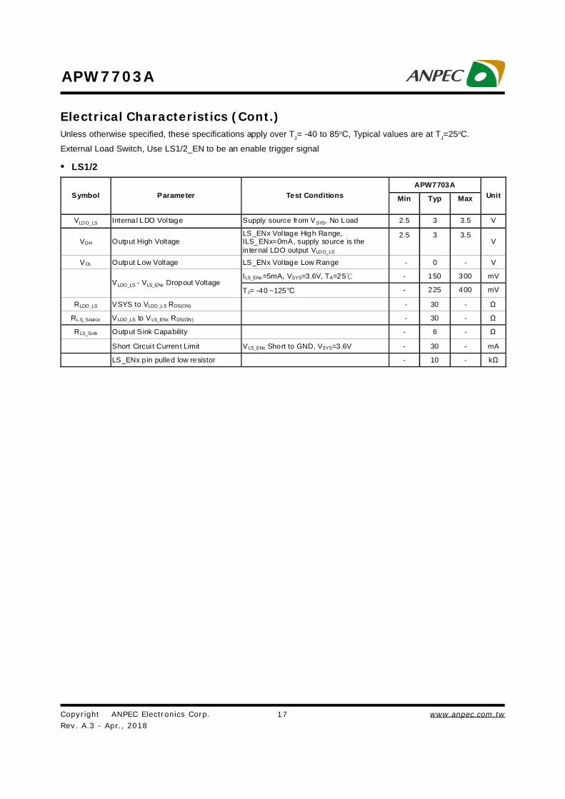
Electrical Characteristics (Cont.)
APW7703A Symbol Parameter Test Conditions Min Typ Max Unit
VLDO_LS Interna l LDO Vol tage Supply source from VSYS, No Load 2.5 3 3.5 V
VOH Output High Voltage LS_ENx Vol tage High Range, ILS_ENx=0mA, supply source is the internal LDO output VLDO_LS
2.5 3 3.5 V
VOL Output Low Voltage LS_ENx Vol tage Low Range - 0 - V
ILS_ENx=5mA, VSYS=3.6V, TA=25 - 150 300 mV VLDO_LS - VLS_ENx Dropout Voltage
TJ= -40 ~125 - 225 400 mV
RLDO_LS VSYS to VLDO_LS RDS(ON) - 30 - Ω
RLS_Source VLDO_LS to VLS_ENx RDS(ON) - 30 - Ω
RLS_Sink Output Sink Capability - 6 - Ω
Short Circui t Current Limit VLS_ENx Short to GND, VSYS=3.6V - 30 - mA
LS_ENx p in pulled low resistor - 10 - kΩ
Unless otherwise specified, these specifications apply over TJ= -40 to 85oC, Typical values are at TJ=25oC.
External Load Switch, Use LS1/2_EN to be an enable trigger signal
• LS1/2

Copyright ANPEC Electronics Corp.Rev. A.3 - Apr., 2018
www.anpec.com.tw18
APW7703A
PIN
NO. NAME FUNCTION
1 WAKEUP2 Input wake up pin to startup the PMIC with a power on event (pulse high)
2 WAKEUP1 Input wake up pin to startup the PMIC with a power on event (pulse high)
3 WAKEUP0 Push-Button input pin. W hen the pin signa l is triggered from low to h igh, the device starts to power up.
4 TS Temperature qua lification voltage input. Connect a negative temperature coefficient thermistor. Program temperature window with a resistor divider from BYPASS to TS pin with 10kΩ. Charge suspends when either TS pin is out of range. Recommend 103AT-2 thermistor.
5 VBAT(CSN) Battery connection point to the positive terminal of the battery pack. The internal BATFET is connected between VBAT and VSYS. Connect a 10µF close ly to the VBAT pin
6 CSP Positive Input o f current sensing Amplifier for charge terminal . A 0.1µF ceramic capacitor is placed from CSP to VBAT (CSN) to provide di fferentia l-mode filtering. An optional 0.1µF ceramic capacitor is placed from CSP pin to PGND for common-mode fil ter ing.
7 BGATE The pin dr ives the gate of an external P-channel MOSFET for the discharge path from battery to system.
8 CHGOUT In switching mode, junction point of the Internal high-side MOSFET Source, output filter inductor and the cathode of the low-side Diode. In linear mode, connet the CHGOUT and VBAT (CSN) togather
9, 10 VSYS System connection point. The external MOSFET is connected between VBAT and VSYS by BGATE Driver signal controled.
11, 12 VBUS Charger input voltage. The internal MOSFET (RBFET) is connected between VBUS and VSYS with VBUS on source. Place a 10µF ceramic capacitor from VBUS to PGND and place it as close as possible to IC.
13 LS2_EN Load switch 2 output enable pin.
14 LX_DC4 DC4 PWM Regulator LX Pin. Connect to externa l inductor for output LC filter.
15 VIN_DC4 DC4 PWM converter Input Pin.
16 FB_DC4 DC4 output feedback vol tage pin.
17 FB_DC2 DC2 output feedback vol tage pin.
18 VIN_DC2 DC2 PWM converter Input Pin.
19 LX_DC2 DC2 PWM Regulator LX Pin. Connect to externa l inductor for output LC filter.
20 LS1_EN Load switch 1 output enable pin.
21 VINLDO2 LDO2 input vol tage pin.
22 LDO2 LDO2 output voltage pin.
23 VINLDO1 LDO1 input vol tage pin.
24 LDO1 LDO1 output voltage pin.
25 FB_LDO1 LDO1 output feedback voltage pin. The LDO1 internal reference is 0.6V.
26 FB_DC1 DC1 output feedback vol tage pin.
27 VIN_DC1 DC1 PWM converter Input Pin.
28 LX_DC1 DC1 PWM Regulator LX Pin. Connect to externa l inductor for output LC filter.
29 PGND
Power ground connection for h igh-current power converter node. Internally, PGND is connected to the anode of the low side diode. On PCB layout, connect directly to ground connection of input and output capacitors of the charger. A single poin t connection is recommended between power PGND and the analog AGND near the IC PGND pin.
30 LX_DC3 DC3 PWM Regulator LX Pin. Connect to externa l inductor for output LC filter.
31 VIN_DC3 DC3 PWM converter Input Pin.
32 FB_DC3 DC3 output feedback vol tage pin.
33 RTCLDO RTCLDO output voltage pin. The pin voltage is adjustable by I2C.
34 BYPASS Intenal bias voltage. It cou ld be the source of resistor-divider for NTC circuit sensing.
Pin Description

Copyright ANPEC Electronics Corp.Rev. A.3 - Apr., 2018
www.anpec.com.tw19
APW7703A
PIN
NO. NAME FUNCTION
35 AGND IC Analog ground.
36 PGOOD Power Good Indicator. Pulled low when either buck converter output is out of regulation.
37 /INT Open interrupt output. Connect the /INT to the pull up ra il via 10kΩ resistor. The /INT pin sends active low, 10µs pulse to host to report charger device status and fault.
38 SDA I2C interface data.
39 SCL I2C inter face clock.
40 CHG_STAT CHG_STAT is an open dra in output used to indicate the sta tus of the various charger operations. When charge in progress, the CHG_STAT is pulled low. CHG_STAT can be used to drive a LED or communicate with a host processor.
Pin Description (Cont.)
Copyright ANPEC Electronics Corp.Rev. A.3 - Apr., 2018
www.anpec.com.tw20
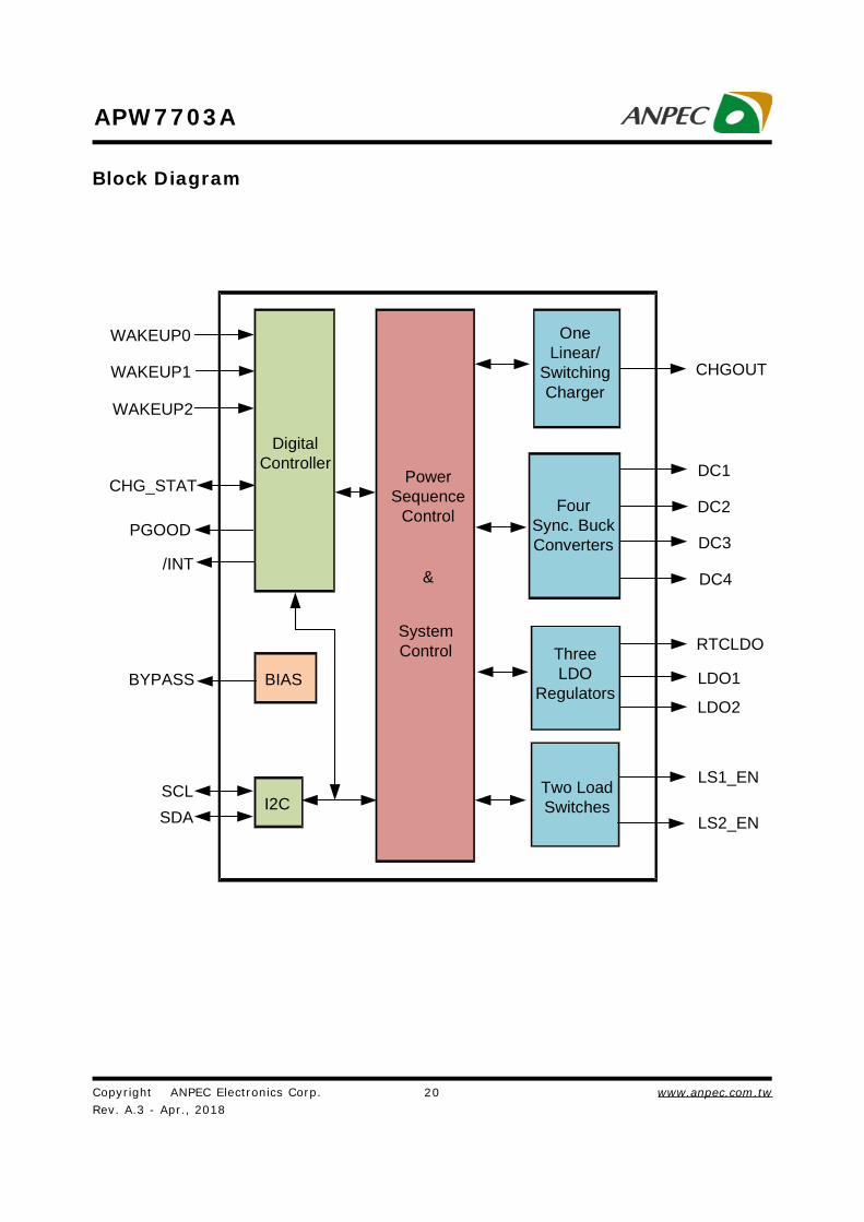
APW7703A
Block Diagram
One Linear/
Switching Charger
Four Sync. Buck Converters
Three LDO
Regulators
Two Load Switches
Power Sequence
Control
&
System Control
CHGOUT
DC1
DC2
DC3
DC4
RTCLDO
LDO1
LDO2
I2C
DigitalController
BIAS
WAKEUP2
CHG_STAT
PGOOD
/INT
BYPASS
SCLSDA
LS1_EN
LS2_EN
WAKEUP1
WAKEUP0

Copyright ANPEC Electronics Corp.Rev. A.3 - Apr., 2018
www.anpec.com.tw21
APW7703A
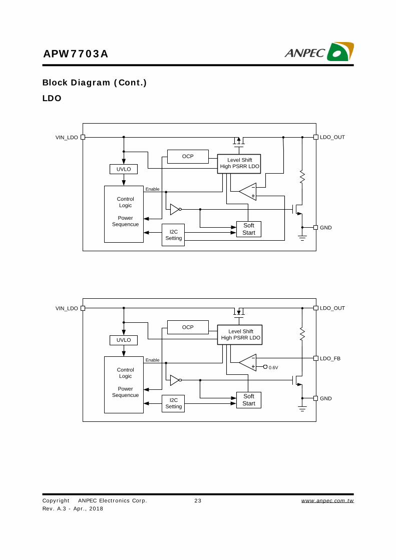
Block Diagram (Cont.)
Charger
VBUS
SYS
BAT
BATFET Gate
Control
PWMSignal
ControllerCHGOUT
Q3
State Machine Controller
104%xVBAT_REGBAT_OVP
VBAT
EN_HIZ
EN_CHG
OCP_BUCKI(Q2)
TS
Battery Thermister
Sensing
TSHUT TSHUT
IC TJ
ITERM
VBAT_REG-VRECHG
VBAT
TERMINATION
RECHG
ICHG
VBATLOWV_F
VBATBATLOWV
VBAT_SHORT
VBATBATSHORT
SUSPEND
ICHG_REG
VBAT_REG
IHSFET_OCP
IINDPM
REF DAC
SDA
SCLI2C
Interface
VINDPM
ICHG_REG
IC TJTREG
VBATVBAT_REG
FBO Q1RBFET Gate
Control
EN_HIZ
REGNLDO
VBAT+VSLEEPSLEEP
UVLO
VACOV
VBUS_UVLOZ
OVP
ICHG
BAT_UVLOVBAT_UVLOZ
Input Current
Limit Control
Q2
BGATE
CSP
ICHGCurrent Sense

Copyright ANPEC Electronics Corp.Rev. A.3 - Apr., 2018
www.anpec.com.tw22
APW7703A
Block Diagram (Cont.)
Buck Converter
LX
GateControl
VREF
FaultLogics
ErrorAmplifier
FB
Inhibit
PGND
POR
Power-On-Reset
SlopeCompensation
CurrentCompartor
CurrentLimit
GateDriver
GateDriver
Gm
IN
VFB
OVP
Current SenseAmplifier
LOC
LOC
SS Ramp,Slew Rate
UVP
Current SenseAmplifier
Zero CrossingComoparator
Oscillator2.4MHz
125%VREF
70%VREF
90%VREF
VFB
AGND
I2C Setting
A/D-D/ASignal Control
PFM CL
Power Sequence
Copyright ANPEC Electronics Corp.Rev. A.3 - Apr., 2018
www.anpec.com.tw23
APW7703A
Block Diagram (Cont.)
LDO
VIN_LDO LDO_OUT
GND
Control Logic
Power Sequencue
UVLO
Enable
OCP
Soft StartI2C
Setting
Level Shift High PSRR LDO
VIN_LDO LDO_OUT
GND
Control Logic
Power Sequencue
UVLO
Enable
OCP
Soft StartI2C
Setting
0.6V
LDO_FB
Level Shift High PSRR LDO
Copyright ANPEC Electronics Corp.Rev. A.3 - Apr., 2018
www.anpec.com.tw24
APW7703A
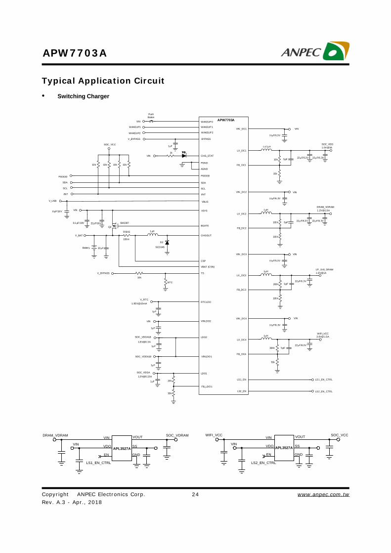
Typical Application Circuit
LDO2
VIN _DC1
LX_DC1
VINLDO2
VINLDO1
FB_LDO1
V_USB
VIN
SOC _VDDA18
SOC_VDDA18
SOC_VDDA
LS1_EN_CTRL
LS2_EN_CTRL
WAKEUP1
10k
1µF
V_RTC
NTC
Q2
1µH
D2
1µF
1µF
1µF
1µF 20k
30k
10µF/16V
VIN
22µF/6.3V
10µF/6.3V
0.47µH
15k
10k
SOC_VDD
FB_DC1
VIN _DC2
LX_DC2
VIN
10µF/6.3V
1µH
100 k
100 k
DRAM_VDRAM
FB_DC2
LX_DC3
22µF/6.3V
1µH
100 k
200 k
LP_1V8_DRAM
FB_DC3
VIN _DC3 VIN
10µF/6.3V
LX_DC4
22µF/6.3V
1µH
91k
364k
WIFI_VCC
FB_DC4
VIN _DC4 VIN
10µF/6.3V
VBUS
VIN
0.1µF/10V
VSYS
Battery 10µF
RSNSCHGOUT
CSP
VBAT (CSN)
V_BAT
BGATE22µF/16V
LDO1
VIN
Push Button
10k
V_BYPASS TS
RTCLDO
WAKEUP0
WAKEUP1
WAKEUP2 WAKEUP2
CHG_STAT
1µF
BYPASSV_BYPASS
SOC_VCC
10k10k 10k
SCL
PGOOD
SDA
/INT
LS1_EN
LS2_EN
PGND
AGND
APW7703A
100m
SM2307
SCL
SDA
/INT
PGOOD
1.95V@10mA
1.0V@3A
1.8V@1A
5pF
SCD345
22µF/6.3V
5pF 22µF/6.3V22µF/6.3V
5pF
5pF
VIN1k
• Switching Charger
VIN
VDO
EN
LS2_EN_CTRL
VIN
WIFI_VCC SOC_VCC
GND
SS
VOUTVIN
VDO
EN
LS1_EN_CTRL
VIN
DRAM_VDRAM SOC_VDRAM
GND
SS
VOUT
APL3527A APL3527A

Copyright ANPEC Electronics Corp.Rev. A.3 - Apr., 2018
www.anpec.com.tw25
APW7703A
Typical Application Circuit
• Linear Charger
LDO2
VIN _DC1
LX_DC1
VINLDO2
VINLDO1
FB_LDO1
V_USB
VIN
SOC _VDDA18
SOC_VDDA18
SOC_VDDA
LS1_EN_CTRL
LS2_EN_CTRL
WAKEUP1
10k
1µF
V_RTC
NTC
Q2
1µF
1µF
1µF
1µF 20k
30k
10µF/16V
VIN
22µF/6.3V
10µF/6.3V
0.47µH
15k
10k
SOC_VDD
FB_DC1
VIN _DC2
LX_DC2
VIN
10µF/6.3V
1µH
100 k
100 k
DRAM_VDRAM
FB_DC2
LX_DC3
22µF/6.3V
1µH
100 k
200 k
LP_1V8_DRAM
FB_DC3
VIN _DC3 VIN
10µF/6.3V
LX_DC4
22µF/6.3V
1µH
91k
364k
WIFI_VCC
FB_DC4
VIN _DC4 VIN
10µF/6.3V
VBUS
VIN
0.1µF/10V
VSYS
Battery 10µF
CHGOUT
CSP
VBAT (CSN)
V_BAT
BGATE22µF/16V
LDO1
VIN
Push Button
10k
V_BYPASS TS
RTCLDO
WAKEUP0
WAKEUP1
WAKEUP2 WAKEUP2
CHG_STAT
1µF
BYPASSV_BYPASS
SOC_VCC
10k10k 10k
SCL
PGOOD
SDA
/INT
LS1_EN
LS2_EN
PGND
AGND
APW7703A
SM2307
SCL
SDA
/INT
PGOOD
1.95V@10mA
1.8V@1A
5pF 22µF/6.3V
5pF 22µF/6.3V22µF/6.3V
5pF
5pF
VIN1k
VIN
VDO
EN
LS2_EN_CTRL
VIN
WIFI_VCC SOC_VCC
GND
SS
VOUTVIN
VDO
EN
LS1_EN_CTRL
VIN
DRAM_VDRAM SOC_VDRAM
GND
SS
VOUT
APL3527A APL3527A

Copyright ANPEC Electronics Corp.Rev. A.3 - Apr., 2018
www.anpec.com.tw26
APW7703A
Power Sequence
No Battery, VBUS Power On
WAKEUPx
RTCLDO
Deglitch Time
DC1
Latch power on sequence
Tr ˜ 750us
DC3
DC2
DC4
Tr ˜ 750us
Tr ˜ 750us
Tr ˜ 750us
LDO2
LS1_EN
LS2_EN
Td ˜ 60msPGOOD
Td ˜ 16ms
Td ˜ 16ms
Td ˜ 16ms
LDO1
VSYS
> 500us
> 1.5V
150us
VBUS
50ms
13ms

Copyright ANPEC Electronics Corp.Rev. A.3 - Apr., 2018
www.anpec.com.tw27
APW7703A
NTC Table and Curve
R_NTC : 10kΩ@25oC
Beta (NTC)= 3380
Temperature
() R_NTC (Ohm ) Gamma (%, V_TS/V_BYPASS)
0 28255 73.86%
5 22614 69.34%
10 18243 64.59%
15 14826 59.72%
20 12136 54.82%
25 10000 50.00%
30 8293 45.33%
35 6919 40.90%
40 5807 36.74%
45 4900 32.89%
50 4157 29.36%
55 3544 26.17%
60 3036 23.29%
65 2612 20.71%
70 2258 18.42%
0, 73.86%
5, 69.34%
10, 64.59%
15, 59.72%
20, 54.82%
25, 50.00%
30, 45.33%
35, 40.90%40, 36.74%
45, 32.89%50, 29.36%
55, 26.17%60, 23.29%
65, 20.71%70, 18.42%
0.00%
10.00%
20.00%
30.00%
40.00%
50.00%
60.00%
70.00%
80.00%
0 10 20 30 40 50 60 70 80
(VTS
/VB
YPAS
S)x
100%
Temperature ( )
[(VTS/VBYPASS) x 100 ] (%) vs Temperature ()

Copyright ANPEC Electronics Corp.Rev. A.3 - Apr., 2018
www.anpec.com.tw28
APW7703A
Layout ConsiderationIn any high switching frequency converter, a correct layout is important to ensure proper operation of the regulator.Below are Layout consideration checklist and demoboard layout for your reference:
Signal Name Pinouts Definition Layout
Input Pins (VBUS, VSYS, VIN_DC1, VIN_DC2, VIN_DC3, VIN_DC4, VINLDO1, VINLDO2)
Charger and All VR’s Power Souce Input Pins
Place the input capacitors on each power source input pins with low impedance to GND and low impedance to the each input pins. Noted that, because VSYS is the all VR’s input power source, the VSYS terminal bulk capacitor is recommended to 22uF/16V and connects to VSYS terminal as close as possible
LX Pins (CHGOUT, LX_DC1, LX_DC2 LX_DC3, LX_DC4)
ALL VR’s LX Pins Keep the switching nodes away from sensitive small signal nodes since these nodes are fast moving signals. Therefore, keep traces to these nodes to inductors as short as possible and there should be no other weak signal traces in parallel with theses traces on any layer. Ideally, route the LX pins to inductors on the top layer is recommended to avoid the switching nodes inteference.
RSNS Charger Current Sence Resistor
The sense resistor should be adjacent to the junction of the inductor and output capacitor. Route the sense leads connected across the RSNS back to the IC, close to each other (minimize loop area) and do not route the sense leads through a high-current path
Feedback Pins (FB_DC1, FB_DC2, FB_DC3, FB_DC4, FB_LDO1)
ALL VR’s output feedback voltage pin.
The pins are high impedance and sensible to noise from the switch node. Coupling from fast switching signals must be avoided. For the better stability, the forward capcitor 5pF from output to feedback is recommended and the feedback divider resistance is recommended as the application circuit.
Bypass pin Intenal bias voltage. It could be the source of resistor-divider for NTC circuit sensing.
Connect the decoupling capacitor to bypass pin as close as possible. The small control signals should be routed away from the high current paths.
Ground (Thermal Pad, PGND, AGND)
IC’s analog and power ground
Connect the IC’s AGND and PGND pad to thermal pad directly. The thermal pad connects to other layer’s ground plane through several vias.

Copyright ANPEC Electronics Corp.Rev. A.3 - Apr., 2018
www.anpec.com.tw29
APW7703A
Layout Consideration (Cont.)
Recommended Minimum Footprint
0.2mm
5mm
0.4mm
.
3.8mm
Exposed forthermal PADconnected
3.8mm5m
m0.3mm
0.6mm
Via diameter=14mil X16
0.3mm

Copyright ANPEC Electronics Corp.Rev. A.3 - Apr., 2018
www.anpec.com.tw30
APW7703A
I2C Programming
The APW7703A DAP has a bidirectional I2C interface that compatible with the I2C (Inter IC) bus protocol and supportsstandard mode (100-kHz), fast mode (400-kHz) and the high-speed mode (up to 3.4Mbps in wire mode) data transferrates for single byte write and read operations. This is a slave only device that does not support a multi-master busenvironment or wait state insertion. The control interface is used to program the registers of the device and to readdevice status.The DAP supports the standard-mode I2C bus operation (100 kHz maximum), the fast I2C bus operation (400 kHzmaximum) and the high-speed mode (up to 3.4Mbps in wire mode). The DAP performs all I2C operations without I2Cwait cycles.
I2C SERIAL CONTROL INTERFACE
The I2C bus uses two signals; SDA (data) and SCL (clock), to communicate between integrated circuits in a system.Data is transferred on the bus serially one bit at a time. The address and data can be transferred in byte (8-bit) format,with the most significant bit (MSB) transferred first. In addition, each byte transferred on the bus is acknowledged by thereceiving device with an acknowledge bit. Each transfer operation begins with the master device driving a startcondition on the bus and ends with the master device driving a stop condition on the bus.The bus uses transitions on the data pin (SDA) while the clock is high to indicate a start and stop conditions. A high-to-low transition on SDA indicates a start and a low-to-high transition indicates a stop. Normal data bit transitions mustoccur within the low time of the clock period. These conditions are shown in Figure 1. The master generates the 7-bitslave address and the R/W bit a zero indicates a transmission (WRITE), a “one” indicates a request for data (READ)to open communication with another device and then waits for an acknowledge condition. The APW7703A holds SDAlow during the acknowledge clock period to indicate an acknowledgment. When this occurs, the master transmits thenext byte of the sequence.Each device is addressed by a unique 7-bit slave address plus R/W bit (1 byte). All compatible devices share thesame signals via a bidirectional bus using a wired-AND connection. An external pull-up resistor must be used for theSDA and SCL signals to set the high level for the bus.
General I2C Operation
Figure 1. Typical I2C sequence
There is no limit on the number of bytes that can be transmitted between start and stop conditions. When the last wordtransfers, the master generates a stop condition to release the bus. A generic data transfer sequence is shown inFigure 1. The device 7-bit address is defined as “0100100” (24H).
7 6 5 4 3 2 1 0 7 6 5 4 3 2 1 0 7 6 5 4 3 2 1 0
7-Bit Slave Address R/W
A 8-Bit Data 8-Bit DataA AASDA
SCL
Start Stop

Copyright ANPEC Electronics Corp.Rev. A.3 - Apr., 2018
www.anpec.com.tw31
APW7703A
I2C Programming (Cont.)
The serial control interface supports single-byte R/W operations for sub-addresses 0x00 to 0xFF.Supplying a sub-address for each sub-address transaction is referred to as random I2C addressing. The APW7703Aalso supports sequential I2C addressing. For write transactions, if a sub-address is issued followed by data for thatsub-address and the 15 sub-addresses that follow, a sequential I2C write transaction has taken place, and the data forall 16 sub-addresses is successfully received by the APW7703A. For I2C sequential write transactions, the sub-address then serves as the start address, and the amount of data subsequently transmitted, before a stop or start istransmitted, determines how many sub-addresses are written. As was true for random addressing, sequential ad-dressing requires that a complete set of data be transmitted. If only a partial set of data is written to the last sub-address, the data for the last sub-address is discarded. However, all other data written is accepted; only the incom-plete data is discarded.
Single-Byte Transfer
As shown in Figure 2, a single-byte data write transfer begins with the master device transmitting a start conditionfollowed by the I2C device address and the R/W bit. The R/W bit determines the direction of the data transfer. For a writedata transfer, the R/W bit will be a 0. After receiving the correct I2C device address and the R/W bit, the DAP respondswith an acknowledge bit. Next, the master transmits the address byte or bytes corresponding to the APW7703A internalmemory address being accessed. After receiving the address byte, the APW7703A again responds with an acknowl-edge bit. Next, the master device transmits the data byte to be written to the memory address being accessed. Afterreceiving the data byte, the APW7703A again responds with an acknowledge bit. Finally, the master device transmitsa stop condition to complete the single-byte data write transfer.
Single-Byte Write
Figure 2. Single-Byte Write Transfer
A6 A5 A4 A3 A2 A1 A0 ACKR/W A6 A5 A4 A3 A2 A1 A0 ACKA7 D6 D5 D4 D3 D2 D1 D0 ACKD7
Start Condition
Stop ConditionI2C Device Address and
Read/ Write BitSub-address Data Byte
AcknowledgeAcknowledgeAcknowledge

Copyright ANPEC Electronics Corp.Rev. A.3 - Apr., 2018
www.anpec.com.tw32
APW7703A
As shown in Figure 3, a single-byte data read transfer begins with the master device transmitting a start conditionfollowed by the I2C device address and the R/W bit. For the data read transfer, both a write followed by a read areactually done. Initially, a write is done to transfer the address byte or bytes of the internal memory address to be read.As a result, the R/W bit becomes a 0. After receiving the APW7703A address and the R/W bit, APW7703A responds withan acknowledge bit. In addition, after sending the internal memory address byte or bytes, the master device transmitsanother start condition followed by the APW7703A address and the R/W bit again. This time the R/W bit becomes a 1,indicating a read transfer. After receiving the address and the R/W bit, the APW7703A again responds with an acknowl-edge bit. Next, the APW7703A transmits the data byte from the memory address being read. After receiving the databyte, the master device transmits a not acknowledge followed by a stop condition to complete the single byte data readtransfer.
Single-Byte Read
Figure 3. Single-Byte Read Transfer
I2C Programming (Cont.)
A6 A5 A1 A0 ACKR/W A6 A1 A0 ACKA7
Start Condition
Stop ConditionI2C Device Address and
Read/ Write BitSub-address
AcknowledgeAcknowledge
A6 A5 A1 A0 R/W
I2C Device Address and Read/ Write Bit
ACK D6 D1 D0 ACKD7
Data Byte
Acknowledge Not Acknowledge
Repeat Start Condition
Copyright ANPEC Electronics Corp.Rev. A.3 - Apr., 2018
www.anpec.com.tw33
APW7703A
I2C Programming (Cont.)
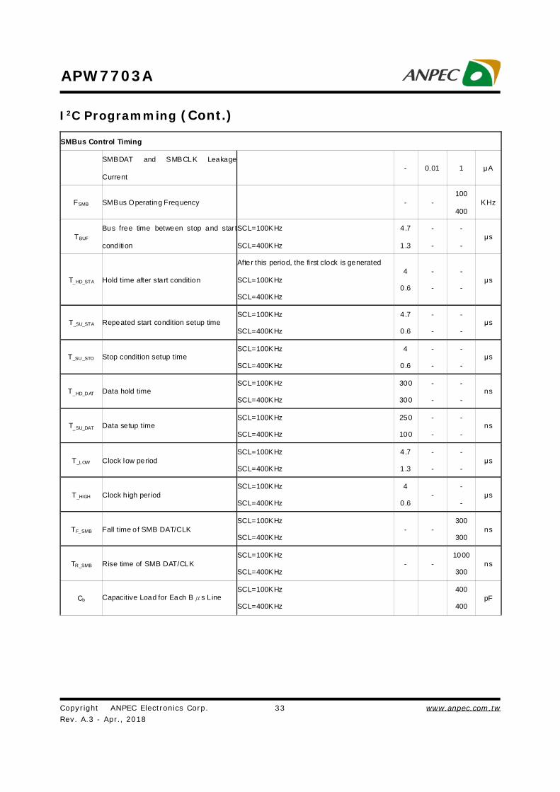
SMBus Control Timing
SMBDAT and SMBCLK Leakage
Current - 0.01 1 μA
FSMB SMBus Operating Frequency - - 100
400 KHz
TBUF Bus free time between stop and star t
condition
SCL=100KHz
SCL=400KHz
4 .7
1 .3
-
-
-
- μs
T_HD_STA Hold time after start condition
After this period, the fi rst clock is generated
SCL=100KHz
SCL=400KHz
4
0 .6
-
-
-
- μs
T_SU_STA Repeated start condition setup time SCL=100KHz
SCL=400KHz
4 .7
0 .6
-
-
-
- μs
T_SU_STO Stop condition setup time SCL=100KHz
SCL=400KHz
4
0 .6
-
-
-
- μs
T_HD_DAT Data hold time SCL=100KHz
SCL=400KHz
300
300
-
-
-
- ns
T_SU_DAT Data setup time SCL=100KHz
SCL=400KHz
250
100
-
-
-
- ns
T_LOW Clock low period SCL=100KHz
SCL=400KHz
4 .7
1 .3
-
-
-
- μs
T_HIGH Clock high per iod SCL=100KHz
SCL=400KHz
4
0 .6 -
-
- μs
TF_SMB Fall time o f SMB DAT/CLK SCL=100KHz
SCL=400KHz - -
300
300 ns
TR_SMB Rise time of SMB DAT/CLK SCL=100KHz
SCL=400KHz - -
1000
300 ns
Cb Capacitive Load for Each Bμs Line SCL=100KHz
SCL=400KHz
400
400 pF

Copyright ANPEC Electronics Corp.Rev. A.3 - Apr., 2018
www.anpec.com.tw34
APW7703A
Timing Diagram
Figure 4: SMBus Common AC Specification
I2C Programming (Cont.)
tBUP
tHD;STA
tLOWtR
tHD;DAT
tF
tHIGH
tSU;DAT tSU;STO
VIH
VIL
VIH
VIL
SMBCLK
SMBDAT
SP S P
tSU;STA
Copyright ANPEC Electronics Corp.Rev. A.3 - Apr., 2018
www.anpec.com.tw35
APW7703A
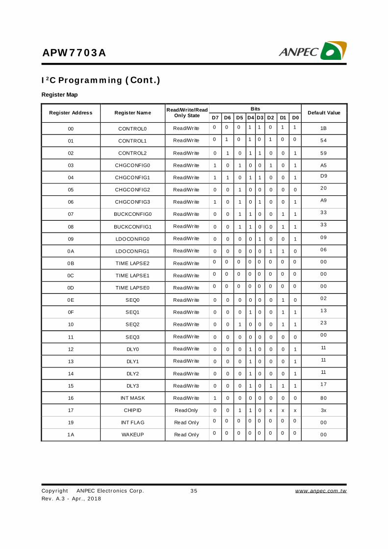
Register Map
Bits Register Address Register Name Read/Write/Read
Only State D7 D6 D5 D4 D3 D2 D1 D0 Default Value
00 CONTROL0 Read/Write 0 0 0 1 1 0 1 1 1B
01 CONTROL1 Read/Write 0 1 0 1 0 1 0 0 54
02 CONTROL2 Read/Write 0 1 0 1 1 0 0 1 59
03 CHGCONFIG0 Read/Write 1 0 1 0 0 1 0 1 A5
04 CHGCONFIG1 Read/Write 1 1 0 1 1 0 0 1 D9
05 CHGCONFIG2 Read/Write 0 0 1 0 0 0 0 0 20
06 CHGCONFIG3 Read/Write 1 0 1 0 1 0 0 1 A9
07 BUCKCONFIG0 Read/Write 0 0 1 1 0 0 1 1 33
08 BUCKCONFIG1 Read/Write 0 0 1 1 0 0 1 1 33
09 LDOCONFIG0 Read/Write 0 0 0 0 1 0 0 1 09
0A LDOCONFIG1 Read/Write 0 0 0 0 0 1 1 0 06
0B TIME LAPSE2 Read/Write 0 0 0 0 0 0 0 0 00
0C TIME LAPSE1 Read/Write 0 0 0 0 0 0 0 0 00
0D TIME LAPSE0 Read/Write 0 0 0 0 0 0 0 0 00
0E SEQ0 Read/Write 0 0 0 0 0 0 1 0 02
0F SEQ1 Read/Write 0 0 0 1 0 0 1 1 13
10 SEQ2 Read/Write 0 0 1 0 0 0 1 1 23
11 SEQ3 Read/Write 0 0 0 0 0 0 0 0 00
12 DLY0 Read/Write 0 0 0 1 0 0 0 1 11
13 DLY1 Read/Write 0 0 0 1 0 0 0 1 11
14 DLY2 Read/Write 0 0 0 1 0 0 0 1 11
15 DLY3 Read/Write 0 0 0 1 0 1 1 1 17
16 INT MASK Read/Write 1 0 0 0 0 0 0 0 80
17 CHIPID ReadOnly 0 0 1 1 0 x x x 3x
19 INT FLAG Read Only 0 0 0 0 0 0 0 0 00
1A WAKEUP Read Only 0 0 0 0 0 0 0 0 00
I2C Programming (Cont.)

Copyright ANPEC Electronics Corp.Rev. A.3 - Apr., 2018
www.anpec.com.tw36
APW7703A
REG00
Bit 7 6 5 4 3 2 1 0
Name WDT_RST RESERVED OFF RSTTMR_EN USB_EN IUSB
Read/Write R/W R/W R/W R/W R/W R/W R/W R/W
Default Value 0 0 0 1 1 0 1 1
Name Description
WDT_RST
Watchdog timer reset bit. Write "1" to reset the watchdog timer when WDT_EN bit is enabled.
0 – Read 0 as usual, write 1 no effect
1 – Write 1 to reset the watchdog timer. (auto clear)
RESERVED No Used
OFF
0 – Normal staus
1 –Trigger a power-down sequence.
Note: When set this bi t to 1 to trigger a power-down sequence. B it is automatical ly reset to 0.
During power down sequence, if the STBYON bit set to "1", the channel will still on.
RSTTMR_EN
Push-button(Wakeup0) reset function enable-disable bit
0 – Disabled
1 – Enabled
USB_EN
USB power path enable
0 – USB power input is turned off (USB suspend mode)
1 – USB power input is turned on
IUSB
USB input current limit
000 – 100mA
001 – 500mA
010 – 900mA
011 – 1300mA
100 – 1700mA
101 – 2100mA
110 – 2500mA
111 – No Used
I2C Programming (Cont.)

Copyright ANPEC Electronics Corp.Rev. A.3 - Apr., 2018
www.anpec.com.tw37
APW7703A
REG01
Bit 7 6 5 4 3 2 1 0
Name LBAT_ALM VLBAT TL_EN RSTTMR RESERVED RESERVED
Read/Write R/W R/W R/W R/W R/W R/W R/W R/W
Default Value 0 1 0 1 0 1 0 0
Name Description
LBAT_ALM
Low battery alarm enable b it
(When alarm is enabled, low battery will automatic power on in sequence when PMIC in OFF mode)
0 – Low battery alarm(3.5V) function disable
1 – Low battery alarm(3.5V) function enable
VLBAT
Low battery alarm voltage threshold setting
000 –3.0V
001 –3.1V
010 –3.2V
011 –3.3V
100 –3.4V
101 –3.5V
110 –3.6V
111 –3.7V
TL_EN
Tim e lapse function enabled bit
0 – time lapse function disable
1 – time lapse function enable
RSTTMR
Push-button(Wakeup0) reset time constant
0 – 8s
1 – 16s
NOTE: Device enters RESET if wakeup0 is held high pulse width for >8s or >16s(default), depending on RSTTMR
bit.
RESERVED No Used
I2C Programming (Cont.)

Copyright ANPEC Electronics Corp.Rev. A.3 - Apr., 2018
www.anpec.com.tw38
APW7703A
REG02
Bit 7 6 5 4 3 2 1 0
Name WDT_EN W DTMR RESERVED RESERVED RESERVED RESERVED
Read/Write R/W R/W R/W R/W R/W R/W R/W R/W
Default Value 0 1 0 1 1 0 0 1
Name Description
WDT_EN
W atchdog timer function enabled bit
0 – watchdog timer function disable
1 – watchdog timer function enab le
Note: W hen WDT_EN is enabled, write "1" to reset WDT_RST bit to reset watchdog timer, if watchdog timer is
timeout, the PMIC wi ll reset al l registers and auto reboot.
WDTMR
W atchdog timer setting bit.
000 – 1s
001 – 2s
010 – 4s
011 – 8s
110 –16s
101 –32s
110 – 64s
111 – 128s
RESERVED No Used
I2C Programming (Cont.)

Copyright ANPEC Electronics Corp.Rev. A.3 - Apr., 2018
www.anpec.com.tw39
APW7703A
REG03
Bit 7 6 5 4 3 2 1 0
Name TIMER TMR_EN CHG_MODE RESERVED TERM RESERVED CHG_EN
Read/Write R/W R/W R/W R/W R/W R/W R/W R/W
Default Value 1 0 1 0 0 1 0 1
Name Description
TIMER
Charge safe ty timer setting (fast charge timer)
00 – 4h
01 – 6h
10 – 8h
11 – 10h
TMR_EN
Safe ty timer enable
0 –Fast charge timer is disabled
1 –Fast charge timer is enabled
CHG_MODE
Charger mode select
0 – Linear charger mode
1 – Switching charger mode
RESERVED No Used
TERM
Charge termination on/off
0 – current-based charge termination will no t occur and the charger will always be on
1 – charge termination enabled, based on t imers and termination current
CHG_EN
Charger enable
0 – charger is disab led
1 – charger is enabled
I2C Programming (Cont.)

Copyright ANPEC Electronics Corp.Rev. A.3 - Apr., 2018
www.anpec.com.tw40
APW7703A
REG04
Bit 7 6 5 4 3 2 1 0
Name DYNTMR VOREG RDIS DIS_EN DISOFF
Read/Write R/W R/W R/W R/W R/W R/W R/W R/W
Default Value 1 1 0 1 1 0 0 1
Name Description
DYNTMR
Dynamic timer function
0 – safety time is the normal setting value
1 – safety timer is 2 times of normal sett ing value if thermal loop or DPM loop is active (Default)
VOREG
Charge voltage selection
0000 – 3.504V 0100 – 3.760V 1000 – 4.016V 1100 – 4 .272V
0001 – 3.568V 0101 – 3.824V 1001 – 4.080V 1101 – 4 .336V
0010 – 3.632V 0110 – 3.888V 1010 – 4.144V 1110 – 4 .400V
0011 – 3.692V 0111 – 3.952V 1011 – 4.208V 1111 – 4 .464V
RDIS
Battery discharge Resistor
0 – 80Ω
1 – 200 Ω
DIS_EN
Discharge enable
0 – battery is not discharged when temperature is above discharge threshold
1 – battery is discharged temperature is above discharge threshold and Vbat > 3.9V
DISOFF
DISCHARGE-OFF threshold (battery is discharged until the battery vol tage drops to):
0 – 3.7V
1 – 3.8V
I2C Programming (Cont.)

Copyright ANPEC Electronics Corp.Rev. A.3 - Apr., 2018
www.anpec.com.tw41
APW7703A
REG05
Bit 7 6 5 4 3 2 1 0
Name ICHG PCHRGT VPRECHG RESERVED IPRECHG
Read/Write R/W R/W R/W R/W R/W R/W R/W R/W
Default Value 0 0 1 0 0 0 0 0
Name Description
ICHG
Charge current setting
Switching Mode, Rsns= 100mΩ;
000 – 128mA 001 – 256mA 010 – 384mA 011 – 512mA
100 – 640mA 101 – 768mA 110 – 896mA 111 – 1024mA
Linear Mode
000 - 100mA 001 - 255mA 010 - 440mA 011 - 640mA
100/101/110/111 - No Used
PCHRGT
Pre-charge time
0 – 30 min
1 – 60 min
VPRECHG
Precharge voltage
0 – pre-charge to fast charge transition voltage is 2.8V
1 – pre-charge to fast charge transition voltage is 3.0V
RESERVED No Used
IPRECHG
Precharge current setting
Switching Mode, Rsns= 100mΩ;
00 – 64mA 01 – 128mA 10 – 192mA 11 – 256mA
Linear Mode
00 - 50mA 01- 100mA 10- 180mA 11- 255mA
I2C Programming (Cont.)
Copyright ANPEC Electronics Corp.Rev. A.3 - Apr., 2018
www.anpec.com.tw42
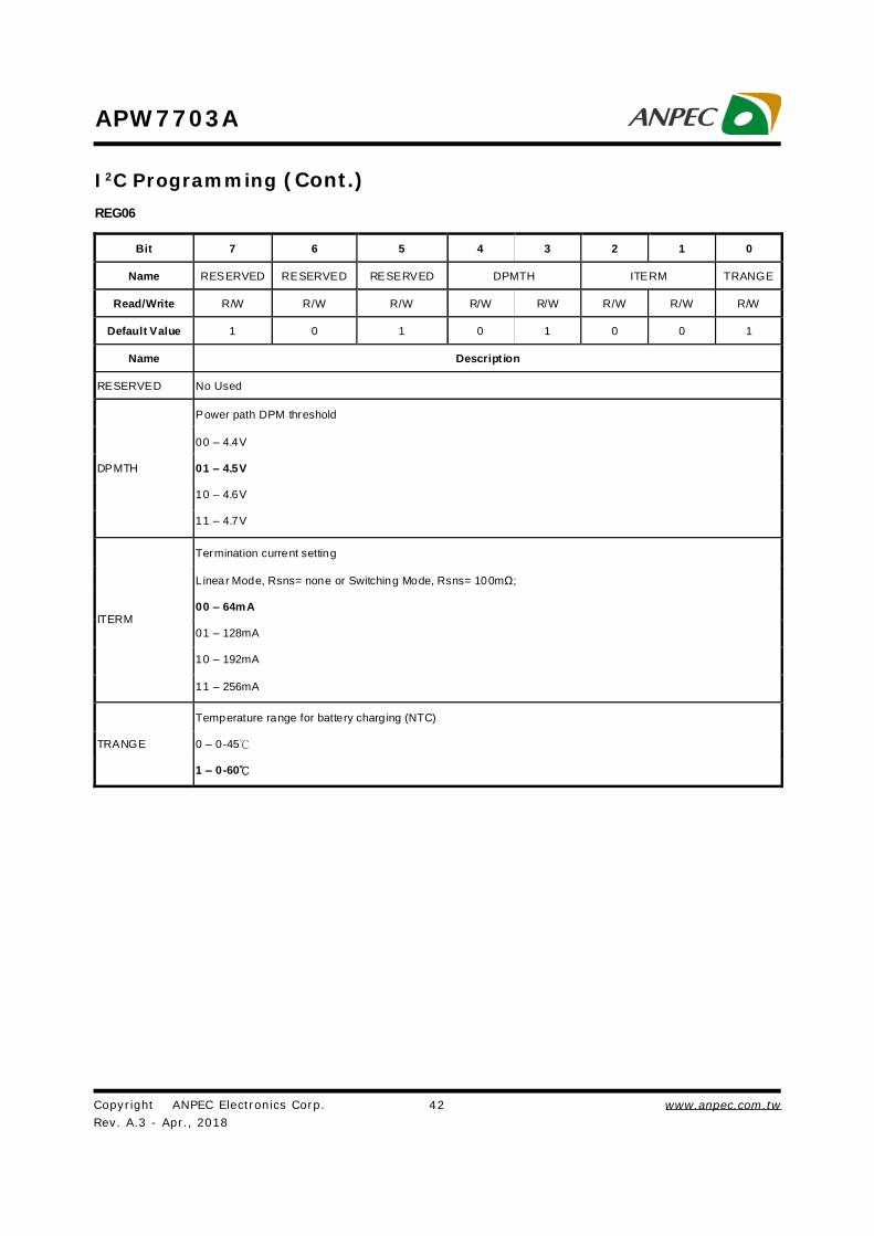
APW7703A
REG06
Bit 7 6 5 4 3 2 1 0
Name RESERVED RESERVED RESERVED DPMTH ITERM TRANGE
Read/Write R/W R/W R/W R/W R/W R/W R/W R/W
Default Value 1 0 1 0 1 0 0 1
Name Descript ion
RESERVED No Used
DPMTH
Power path DPM threshold
00 – 4.4V
01 – 4.5V
10 – 4.6V
11 – 4.7V
ITERM
Termination current setting
Linear Mode, Rsns= none or Switching Mode, Rsns= 100mΩ;
00 – 64mA
01 – 128mA
10 – 192mA
11 – 256mA
TRANGE
Temperature range for battery charg ing (NTC)
0 – 0-45
1 – 0-60
I2C Programming (Cont.)

Copyright ANPEC Electronics Corp.Rev. A.3 - Apr., 2018
www.anpec.com.tw43
APW7703A
REG07
Bit 7 6 5 4 3 2 1 0
Name STBYON_DC1 VFB_DC1 STBYON_DC2 VFB_DC2
Read/Write R/W R/W R/W R/W R/W R/W R/W R/W
Default Value 0 0 1 1 0 0 1 1
Name Descript ion
STBYON_DC1
Off mode DC1 regulator enabled bit
0 – power off as sequence
1 – still enable in OFF mode
VFB_DC1
VFB_DC1 voltage setting
000 – 0.555V
001 – 0.570V
010 – 0.585V
011 – 0.600V
100 – 0.615V
101 – 0.630V
110 – 0.645V
111 – 0.660V
STBYON_DC2
Off mode DC2 regulator enabled bit
0 – power off as sequence
1 – still enable in OFF mode
VFB_DC2
VFB_DC2 voltage setting
000 – 0.555V
001 – 0.570V
010 – 0.585V
011 – 0.600V
100 – 0.615V
101 – 0.630V
110 – 0.645V
111 – 0.660V
I2C Programming (Cont.)

Copyright ANPEC Electronics Corp.Rev. A.3 - Apr., 2018
www.anpec.com.tw44
APW7703A
REG08
Bit 7 6 5 4 3 2 1 0
Name STBYON_DC3 VFB_DC3 STBYON_DC4 VFB_DC4
Read/Write R/W R/W R/W R/W R/W R/W R/W R/W
Default Value 0 0 1 1 0 0 1 1
Name Descript ion
STBYON_DC3
Off mode DC3 regulator enabled bit
0 – power off as sequence
1 – still enable in OFF mode
VFB_DC3
VFB_DC3 voltage setting
000 – 0.555V
001 – 0.570V
010 – 0.585V
011 – 0.600V
100 – 0.615V
101 – 0.630V
110 – 0.645V
111 – 0.660V
STBYON_DC4
Off mode DC4 regulator enabled bit
0 – power off as sequence
1 – still enable in OFF mode
VFB_DC4
VFB_DC4 voltage setting
000 – 0.555V
001 – 0.570V
010 – 0.585V
011 – 0.600V
100 – 0.615V
101 – 0.630V
110 – 0.645V
111 – 0.660V
I2C Programming (Cont.)

Copyright ANPEC Electronics Corp.Rev. A.3 - Apr., 2018
www.anpec.com.tw45
APW7703A
REG09
Bit 7 6 5 4 3 2 1 0
Name RESERVED RESERVED RESERVED RTCLDO
Read/Write R/W R/W R/W R/W R/W R/W R/W R/W
Default Value 0 0 0 0 1 0 0 1
Name Description
RESERVED No Used
RTCLDO
RTCLDO output voltage setting
00000 – 1.5V 00001 – 1.55V 00010 – 1.6V 00011 – 1.65V
00100 – 1.7V 00101 – 1.75V 00110 – 1.8V 00111 – 1.85V
01000 – 1.9V 01001 – 1.95V 01010 – 2.0V 01011 – 2.05V
01100 – 2.1V 01101 – 2.15V 01110 – 2.2V 01111 – 2.25V
10000 – 2.3V 10001 – 2.35V 10010 – 2.4V 10011 – 2.45V
10100 – 2.5V 10101 – 2.55V 10110 – 2.6V 10111 – 2.65V
11000 – 2.7V 11001 – 2.75V 11010 – 2.8V 11011 – 2.85V
11100 – 2.9V 11101 – 2.95V 11110 – 3.0V 11111 – 3.05V
I2C Programming (Cont.)

Copyright ANPEC Electronics Corp.Rev. A.3 - Apr., 2018
www.anpec.com.tw46
APW7703A
I2C Programming (Cont.)REG0A
Bit 7 6 5 4 3 2 1 0
Name STBYON_LDO1 STBYON_LDO2 RESERVED LDO2
Read/Write R/W R/W R/W R/W R/W R/W R/W R/W
Default Value 0 0 0 0 0 1 1 0
Name Description
STBY_ON_LDO1
Standby mode regulator enabled bit
0 – power off as sequence
1 – still enable in OFF mode
STBY_ON_LDO2
Standby mode regulator enabled bit
0 – power off as sequence
1 – still enable in OFF mode
RESERVED No Used
LDO2
LDO2 output voltage setting
0 0000 – 1.50V 0 0001 – 1.55V 0 0010 – 1.60V 0 0011 – 1.65V 0 0100 – 1.70V 0 0101 – 1.75V 0 0110 – 1.80V
0 0111 – 1.85V 0 1000 – 1.90V 0 1001 – 1.95V 0 1010 – 2.00V 0 1011 – 2.05V 0 1100 – 2.10V 0 1101 – 2.15V
0 1110 – 2.20V 0 1111 – 2.25V 1 0000 – 2.30V 1 0001 – 2.35V 1 0010 – 2.40V 1 0011 – 2.45V 1 0100 – 2.50V
1 0101 – 2.55V 1 0110 – 2.60V 1 0111 – 2.65V 1 1000 – 2.70V 1 1001 – 2.75V 1 1010 – 2.80V 1 1011 – 2.85V
1 1100 – 2.90V 1 1101 – 2.95V 1 1110 – 3.00V 1 1111 – 3.05V

Copyright ANPEC Electronics Corp.Rev. A.3 - Apr., 2018
www.anpec.com.tw47
APW7703A
REG0B
Bit 7 6 5 4 3 2 1 0
Name T23 T22 T21 T20 T19 T18 T17 T16
Read/Write R/W R/W R/W R/W R/W R/W R/W R/W
Default Value 0 0 0 0 0 0 0 0
Name Description
T23~T0
Time lapse length setting in second
00000000 00000000 00000000 - 1sec
……
11111111 11111111 11111111 - 16777216sec (194D 4H 20M 16S)
I2C Programming (Cont.)
REG0C
Bit 7 6 5 4 3 2 1 0
Name T15 T14 T13 T12 T11 T10 T09 T08
Read/Write R/W R/W R/W R/W R/W R/W R/W R/W
Default Value 0 0 0 0 0 0 0 0
Name Description
T23~T0
Time lapse length setting in second
00000000 00000000 00000000 - 1sec
……
11111111 11111111 11111111 - 16777216sec (194D 4H 20M 16S)
REG0D
Bit 7 6 5 4 3 2 1 0
Name T07 T06 T05 T04 T03 T02 T01 T00
Read/Write R/W R/W R/W R/W R/W R/W R/W R/W
Default Value 0 0 0 0 0 0 0 0
Name Description
T23~T0
Time lapse length setting in second
00000000 00000000 00000000 - 1sec
……
11111111 11111111 11111111 - 16777216sec (194D 4H 20M 16S)
Copyright ANPEC Electronics Corp.Rev. A.3 - Apr., 2018
www.anpec.com.tw48
APW7703A
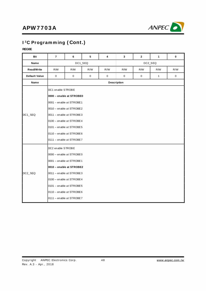
REG0E
Bit 7 6 5 4 3 2 1 0
Name DC1_SEQ DC2_SEQ
Read/Write R/W R/W R/W R/W R/W R/W R/W R/W
Default Value 0 0 0 0 0 0 1 0
Name Description
DC1_SEQ
DC1 enable STROBE
0000 – enable at STROBE0
0001 – enable a t STROBE1
0010 – enable a t STROBE2
0011 – enable a t STROBE3
0100 – enable a t STROBE4
0101 – enable a t STROBE5
0110 – enable a t STROBE6
0111 – enable a t STROBE7
DC2_SEQ
DC2 enable STROBE
0000 – enable a t STROBE0
0001 – enable a t STROBE1
0010 – enable at STROBE2
0011 – enable a t STROBE3
0100 – enable a t STROBE4
0101 – enable a t STROBE5
0110 – enable a t STROBE6
0111 – enable a t STROBE7
I2C Programming (Cont.)

Copyright ANPEC Electronics Corp.Rev. A.3 - Apr., 2018
www.anpec.com.tw49
APW7703A
REG0F
Bit 7 6 5 4 3 2 1 0
Name DC3_SEQ DC4_SEQ
Read/Write R/W R/W R/W R/W R/W R/W R/W R/W
Default Value 0 0 0 1 0 0 1 1
Name Description
DC3_SEQ
DC3 enable STROBE
0000 – enable a t STROBE0
0001 – enable at STROBE1
0010 – enable a t STROBE2
0011 – enable a t STROBE3
0100 – enable a t STROBE4
0101 – enable a t STROBE5
0110 – enable a t STROBE6
0111 – enable a t STROBE7
DC4_SEQ
DC4 enable STROBE
0000 – enable a t STROBE0
0001 – enable a t STROBE1
0010 – enable a t STROBE2
0011 – enable at STROBE3
0100 – enable a t STROBE4
0101 – enable a t STROBE5
0110 – enable a t STROBE6
0111 – enable a t STROBE7
I2C Programming (Cont.)
Copyright ANPEC Electronics Corp.Rev. A.3 - Apr., 2018
www.anpec.com.tw50
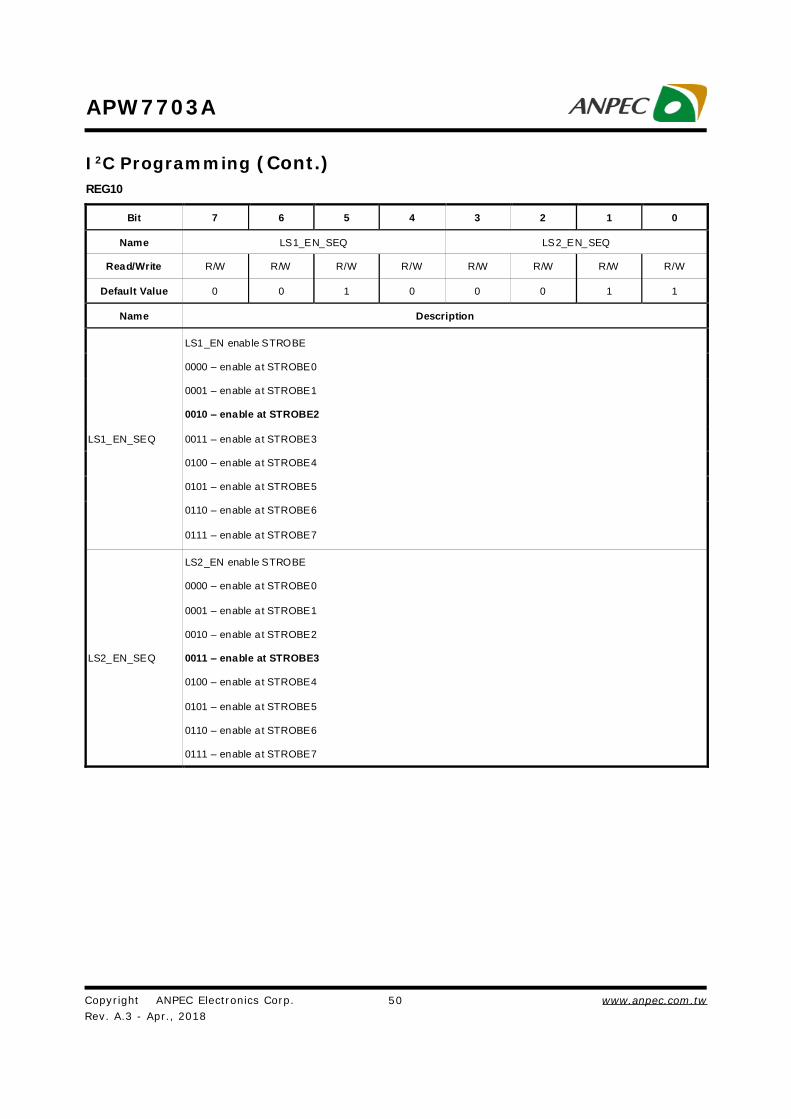
APW7703A
REG10
Bit 7 6 5 4 3 2 1 0
Name LS1_EN_SEQ LS2_EN_SEQ
Read/Write R/W R/W R/W R/W R/W R/W R/W R/W
Default Value 0 0 1 0 0 0 1 1
Name Description
LS1_EN_SEQ
LS1_EN enable STROBE
0000 – enable a t STROBE0
0001 – enable a t STROBE1
0010 – enable at STROBE2
0011 – enable a t STROBE3
0100 – enable a t STROBE4
0101 – enable a t STROBE5
0110 – enable a t STROBE6
0111 – enable a t STROBE7
LS2_EN_SEQ
LS2_EN enable STROBE
0000 – enable a t STROBE0
0001 – enable a t STROBE1
0010 – enable a t STROBE2
0011 – enable at STROBE3
0100 – enable a t STROBE4
0101 – enable a t STROBE5
0110 – enable a t STROBE6
0111 – enable a t STROBE7
I2C Programming (Cont.)

Copyright ANPEC Electronics Corp.Rev. A.3 - Apr., 2018
www.anpec.com.tw51
APW7703A
REG11
Bit 7 6 5 4 3 2 1 0
Name LDO1_SEQ LDO2_SEQ
Read/Write R/W R/W R/W R/W R/W R/W R/W R/W
Default Value 0 0 0 0 0 0 0 0
Name Description
LDO1_SEQ
LDO1 enable STROBE
0000 – enable at STROBE0
0001 – enable a t STROBE1
0010 – enable a t STROBE2
0011 – enable a t STROBE3
0100 – enable a t STROBE4
0101 – enable a t STROBE5
0110 – enable a t STROBE6
0111 – enable a t STROBE7
LDO2_SEQ
LDO2 enable STROBE
0000 – enable at STROBE0
0001 – enable a t STROBE1
0010 – enable a t STROBE2
0011 – enable a t STROBE3
0100 – enable a t STROBE4
0101 – enable a t STROBE5
0110 – enable a t STROBE6
0111 – enable a t STROBE7
I2C Programming (Cont.)

Copyright ANPEC Electronics Corp.Rev. A.3 - Apr., 2018
www.anpec.com.tw52
APW7703A
REG12
Bit 7 6 5 4 3 2 1 0
Name DLY1 DLY2
Read/Write R/W R/W R/W R/W R/W R/W R/W R/W
Default Value 0 0 0 1 0 0 0 1
Name Description
DLY1
Delay 1 time (Between STROBE0 and STROBLE1)
0000 – 12ms 0100 – 28ms 1000 – 44ms 1100 – 60ms
0001 – 16ms 0101 – 32ms 1001 – 48ms 1101 – 64ms
0010 – 20ms 0110 – 36ms 1010 – 52ms 1110 – 68ms
0011 – 24ms 0111 – 40ms 1011 – 56ms 1111 – 72ms
DLY2
Delay 2 time (Between STROBE1 and STROBLE2)
0000 – 12ms 0100 – 28ms 1000 – 44ms 1100 – 60ms
0001 – 16ms 0101 – 32ms 1001 – 48ms 1101 – 64ms
0010 – 20ms 0110 – 36ms 1010 – 52ms 1110 – 68ms
0011 – 24ms 0111 – 40ms 1011 – 56ms 1111 – 72ms
I2C Programming (Cont.)
REG13
Bit 7 6 5 4 3 2 1 0
Name DLY3 DLY4
Read/Write R/W R/W R/W R/W R/W R/W R/W R/W
Default Value 0 0 0 1 0 0 0 1
Name Description
DLY3
Delay 3 time (Between STROBE2 and STROBLE3)
0000 – 12ms 0100 – 28ms 1000 – 44ms 1100 – 60ms
0001 – 16ms 0101 – 32ms 1001 – 48ms 1101 – 64ms
0010 – 20ms 0110 – 36ms 1010 – 52ms 1110 – 68ms
0011 – 24ms 0111 – 40ms 1011 – 56ms 1111 – 72ms
DLY4
Delay 4 time (Between STROBE3 and STROBLE4)
0000 – 12ms 0100 – 28ms 1000 – 44ms 1100 – 60ms
0001 – 16ms 0101 – 32ms 1001 – 48ms 1101 – 64ms
0010 – 20ms 0110 – 36ms 1010 – 52ms 1110 – 68ms
0011 – 24ms 0111 – 40ms 1011 – 56ms 1111 – 72ms

Copyright ANPEC Electronics Corp.Rev. A.3 - Apr., 2018
www.anpec.com.tw53
APW7703A
REG14
Bit 7 6 5 4 3 2 1 0
Nam e DLY5 DLY6
Read/Write R/W R/W R/W R/W R/W R/W R/W R/W
Default Va lue 0 0 0 1 0 0 0 1
Nam e Description
DLY5
Delay 5 time (Between STROBE4 and STROB LE5)
0000 – 12ms 0100 – 28ms 1000 – 44ms 1100 – 60ms
0001 – 16m s 0101 – 32ms 1001 – 48ms 1101 – 64ms
0010 – 20ms 0110 – 36ms 1010 – 52ms 1110 – 68ms
0011 – 24ms 0111 – 40ms 1011 – 56ms 1111 – 72ms
DLY6
Delay 6 time (Between STROBE5 and STROB LE6)
0000 – 12ms 0100 – 28ms 1000 – 44ms 1100 – 60ms
0001 – 16m s 0101 – 32ms 1001 – 48ms 1101 – 64ms
0010 – 20ms 0110 – 36ms 1010 – 52ms 1110 – 68ms
0011 – 24ms 0111 – 40ms 1011 – 56ms 1111 – 72ms
I2C Programming (Cont.)
REG15
Bit 7 6 5 4 3 2 1 0
Nam e DLY7 PG DLY
Read/Write R/W R/W R/W R/W R/W R/W R/W R/W
Default Va lue 0 0 0 1 0 1 1 1
Nam e Description
DLY7
Delay 7 time (Between STROBE6 and STROB LE7)
0000 – 12ms 0100 – 28ms 1000 – 44ms 1100 – 60ms
0001 – 16m s 0101 – 32ms 1001 – 48ms 1101 – 64ms
0010 – 20ms 0110 – 36ms 1010 – 52ms 1110 – 68ms
0011 – 24ms 0111 – 40ms 1011 – 56ms 1111 – 72ms
PGDLY
Power Good Delay time
0000 – 10ms 0100 – 40ms 1000 – 72ms 1100 – 104ms
0001 – 16ms 0101 – 48ms 1001 – 80ms 1101 – 112ms
0010 – 24ms 0110 – 56ms 1010 – 88ms 1110 – 120ms
0011 – 32ms 0111 – 64ms 1011 – 96ms 1111 – 128ms
Note PG DLY applies to PGOOD p in.
Copyright ANPEC Electronics Corp.Rev. A.3 - Apr., 2018
www.anpec.com.tw54
APW7703A
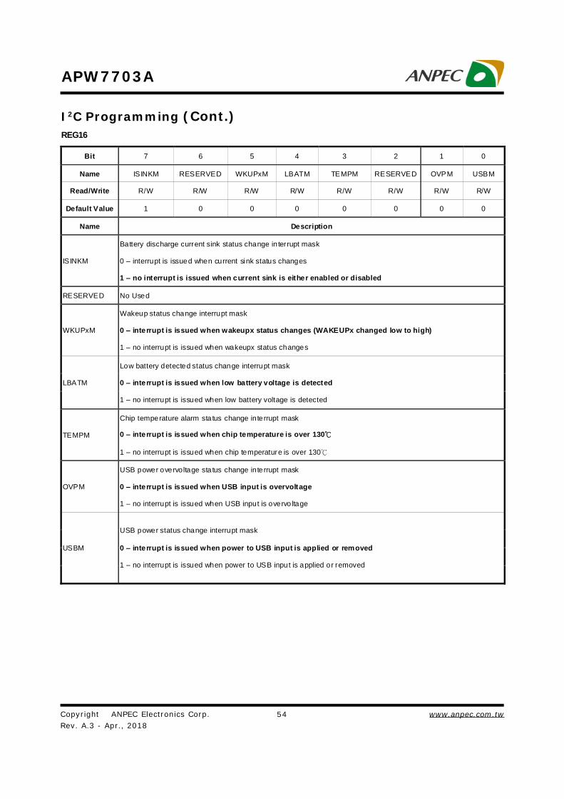
REG16
Bit 7 6 5 4 3 2 1 0
Name ISINKM RESERVED WKUPxM LBATM TEMPM RESERVED OVPM USBM
Read/Write R/W R/W R/W R/W R/W R/W R/W R/W
Default Value 1 0 0 0 0 0 0 0
Name Description
IS INKM
Battery discharge current sink status change in terrupt mask
0 – interrupt is issued when current sink status changes
1 – no interrupt is issued when current sink is either enabled or disabled
RESERVED No Used
WKUPxM
Wakeup status change interrupt mask
0 – interrupt is issued when wakeupx status changes (WAKEUPx changed low to high)
1 – no interrupt is issued when wakeupx status changes
LBATM
Low battery detected status change interrupt mask
0 – interrupt is issued when low battery voltage is detected
1 – no interrupt is issued when low battery voltage is detected
TEMPM
Chip temperature alarm sta tus change interrupt mask
0 – interrupt is issued when chip temperature is over 130
1 – no interrupt is issued when chip temperature is over 130
OVPM
USB power overvoltage sta tus change interrupt mask
0 – interrupt is issued when USB input is overvoltage
1 – no interrupt is issued when USB input is overvo ltage
USBM
USB power status change interrupt mask
0 – interrupt is issued when power to USB input is applied or removed
1 – no interrupt is issued when power to USB input is applied or removed
I2C Programming (Cont.)

Copyright ANPEC Electronics Corp.Rev. A.3 - Apr., 2018
www.anpec.com.tw55
APW7703A
REG17
Bit 7 6 5 4 3 2 1 0
Name RESERVED CHIPID RESERVED REV
Read/Write R R R R R R R R
Default Value 0 0 1 1 0 x x x
Name Description
RESERVED No Used
CHIP ID Chip ID
011 – APW7703A
REV
Revision
000 – revision 1.0
001 – revision 1.1
010 – revision 1.2
011 – revision 1.3
…
111 - Future Use
I2C Programming (Cont.)
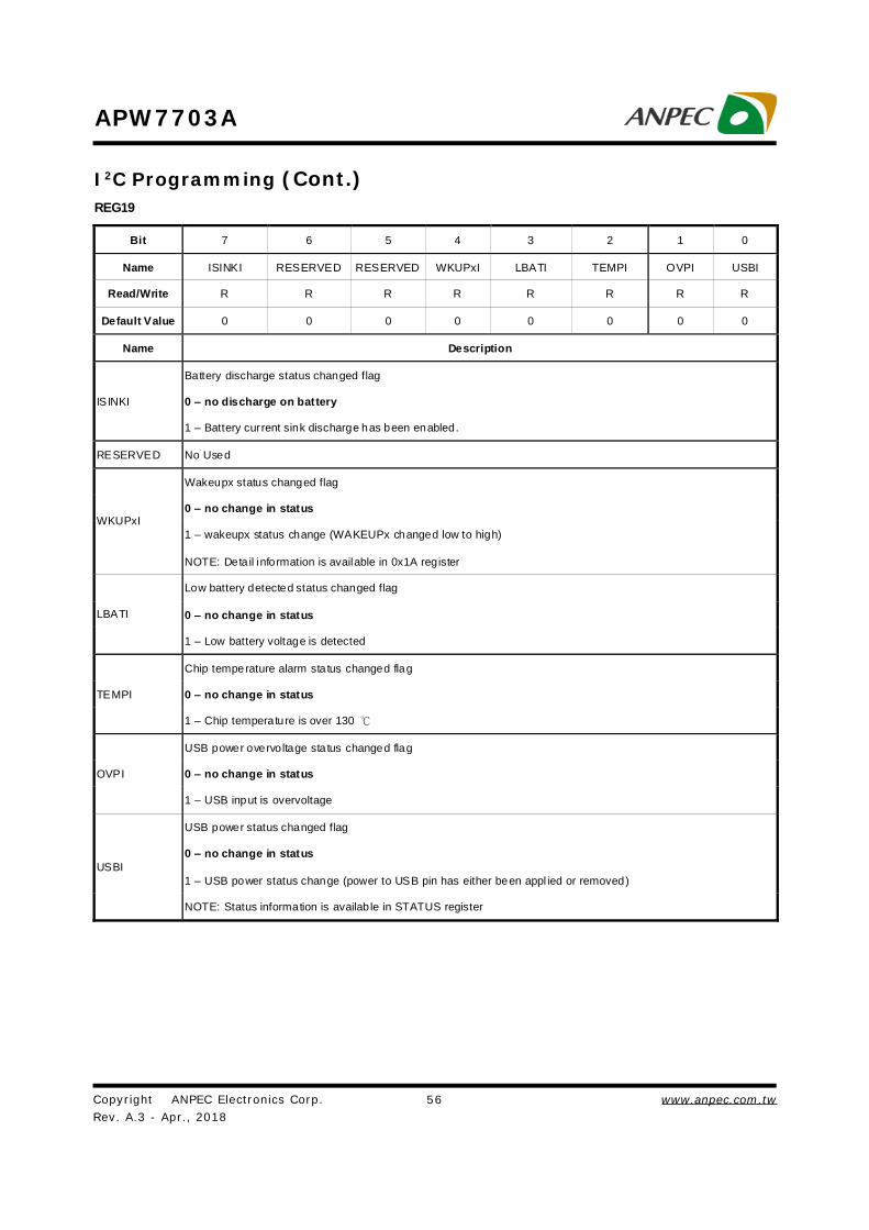
Copyright ANPEC Electronics Corp.Rev. A.3 - Apr., 2018
www.anpec.com.tw56
APW7703A
REG19
Bit 7 6 5 4 3 2 1 0
Name ISINKI RESERVED RESERVED WKUPxI LBATI TEMPI OVPI USBI
Read/Write R R R R R R R R
Default Value 0 0 0 0 0 0 0 0
Name Description
IS INKI
Battery discharge status changed flag
0 – no discharge on battery
1 – Battery current sink discharge has been enabled.
RESERVED No Used
Wakeupx status changed flag
0 – no change in status WKUPxI
1 – wakeupx status change (WAKEUPx changed low to high)
NOTE: Deta il information is available in 0x1A register
Low battery detected status changed flag
0 – no change in status LBATI
1 – Low battery voltage is detected
Chip temperature alarm sta tus changed flag
0 – no change in status TEMPI
1 – Chip temperature is over 130
USB power overvoltage sta tus changed flag
0 – no change in status OVPI
1 – USB input is overvoltage
USB power status changed flag
0 – no change in status
1 – USB power status change (power to USB pin has either been appl ied or removed) USBI
NOTE: Status information is availab le in STATUS register
I2C Programming (Cont.)
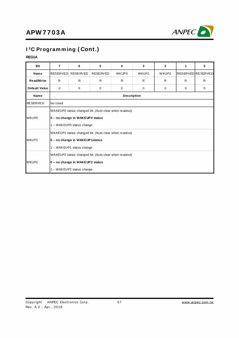
Copyright ANPEC Electronics Corp.Rev. A.3 - Apr., 2018
www.anpec.com.tw57
APW7703A
REG1A
Bit 7 6 5 4 3 2 1 0
Name RESERVED RESERVED RESERVED WKUP0 WKUP1 W KUP2 RESERVED RESERVED
Read/Write R R R R R R R R
Default Value 0 0 0 0 0 0 0 0
Name Description
RESERVED No Used
WKUP0
WAKEUP0 status changed bit. (Auto clear when readout)
0 – no change in WAKEUP0 status
1 – WAKEUP0 status change
WKUP1
WAKEUP1 status changed bit. (Auto clear when readout)
0 – no change in WAKEUP1status
1 – WAKEUP1 status change
WKUP2
WAKEUP2 status changed bit. (Auto clear when readout)
0 – no change in WAKEUP2 status
1 – WAKEUP2 status change
I2C Programming (Cont.)
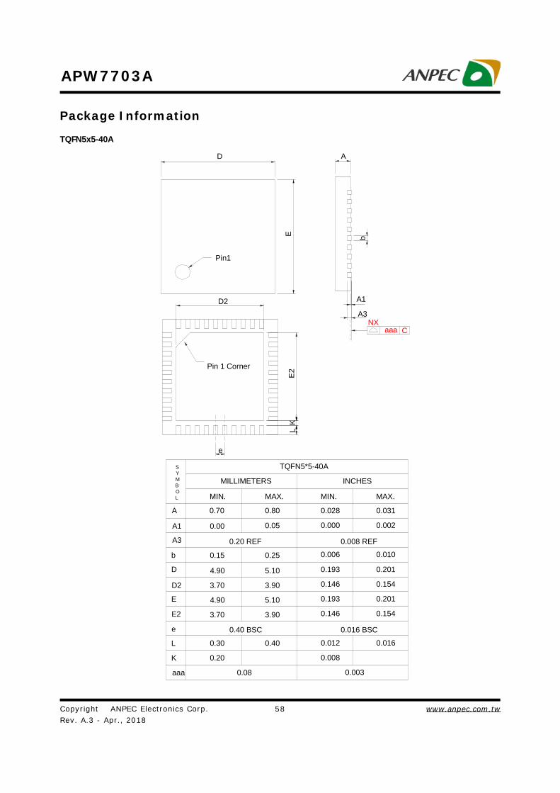
Copyright ANPEC Electronics Corp.Rev. A.3 - Apr., 2018
www.anpec.com.tw58
APW7703A
Package Information
TQFN5x5-40A
D
E
Pin1
A
b
A1
A3NX
aaa C
D2E
2Pin 1 Corner
e
KL
0.70
0.154
0.028
0.002
0.40 BSC 0.016 BSC
aaa 0.08 0.003
3.70 3.90
0.20 0.008K
4.90 5.10 0.193 0.201
4.90 5.10 0.193 0.201
SYMBOL MIN. MAX.
0.80
0.00
0.15 0.25
3.70 3.90
0.05
A
A1
b
D
D2
E
E2
e
L
MILLIMETERS
A3 0.20 REF
TQFN5*5-40A
0.30 0.40
0.008 REF
MIN. MAX.
INCHES
0.031
0.000
0.006 0.010
0.146 0.154
0.146
0.012 0.016

Copyright ANPEC Electronics Corp.Rev. A.3 - Apr., 2018
www.anpec.com.tw59
APW7703A
Carrier Tape & Reel Dimensions
H
T1
A
d
A
E1
AB
W
F
T
P0OD0
BA0
P2
K0
B0
SECTION B-B
SECTION A-A
OD1
P1
Application A H T1 C d D W E1 F
330.0±2.00 50 MIN. 12.4+2.00 -0.00
13.0+0.50 -0.20
1.5 MIN. 20.2 MIN. 12.0±0.30 1.75±0.10 5.5±0.10
P0 P1 P2 D0 D1 T A0 B0 K0 TQFN 5x5
4.0±0.10 8.0±0.10 2.0±0.10 1.5+0.10 -0.00 1.5 MIN. 0.6+0.00
-0.40 5.35±0.20 5.35±0.20 1.00±0.20
(mm)
Package Type Unit Quantity
TQFN5x5-40A Tape & Reel 2500
Devices Per Unit

Copyright ANPEC Electronics Corp.Rev. A.3 - Apr., 2018
www.anpec.com.tw60
APW7703A
Taping Direction Information
TQFN5x5-40A
Classification Profile
USER DIRECTION OF FEED

Copyright ANPEC Electronics Corp.Rev. A.3 - Apr., 2018
www.anpec.com.tw61
APW7703A
Profile Feature Sn-Pb Eutectic Assembly Pb-Free Assembly
Preheat & Soak Temperature min (Tsmin) Temperature max (Tsmax) Time (Tsmin to Tsmax) (ts)
100 °C 150 °C
60-120 seconds
150 °C 200 °C
60-120 seconds
Average ramp-up rate (Tsmax to TP) 3 °C/second max. 3°C/second max.
Liquidous temperature (TL) Time at liquidous (tL)
183 °C 60-150 seconds
217 °C 60-150 seconds
Peak package body Temperature (Tp)*
See Classification Temp in table 1 See Classification Temp in table 2
Time (tP)** within 5°C of the specified classification temperature (Tc)
20** seconds 30** seconds
Average ramp-down rate (Tp to Tsmax) 6 °C/second max. 6 °C/second max.
Time 25°C to peak temperature 6 minutes max. 8 minutes max.
* Tolerance for peak profile Temperature (Tp) is defined as a supplier minimum and a user maximum. ** Tolerance for time at peak profile temperature (tp) is defined as a supplier minimum and a user maximum.
Classification Reflow Profiles
Table 2. Pb-free Process – Classification Temperatures (Tc) Package
Thickness Volume mm3
<350 Volume mm3
350-2000 Volume mm3
>2000 <1.6 mm 260 °C 260 °C 260 °C
1.6 mm – 2.5 mm 260 °C 250 °C 245 °C ≥2.5 mm 250 °C 245 °C 245 °C
Table 1. SnPb Eutectic Process – Classification Temperatures (Tc)
Package Thickness
Volume mm3
<350 Volume mm3
≥350 <2.5 mm 235 °C 220 °C ≥2.5 mm 220 °C 220 °C
Reliability Test Program
Test item Method Description SOLDERABILITY JESD-22, B102 5 Sec, 245°C HOLT JESD-22, A108 1000 Hrs, Bias @ Tj=125°C PCT JESD-22, A102 168 Hrs, 100%RH, 2atm, 121°C TCT JESD-22, A104 500 Cycles, -65°C~150°C HBM MIL-STD-883-3015.7 VHBM≧2KV MM JESD-22, A115 VMM≧200V Latch-Up JESD 78 10ms, 1tr≧100mA

Copyright ANPEC Electronics Corp.Rev. A.3 - Apr., 2018
www.anpec.com.tw62
APW7703A
Customer Service
Anpec Electronics Corp.Head Office :
No.6, Dusing 1st Road, SBIP,Hsin-Chu, Taiwan, R.O.C.Tel : 886-3-5642000Fax : 886-3-5642050
Taipei Branch :2F, No. 11, Lane 218, Sec 2 Jhongsing Rd.,Sindian City, Taipei County 23146, TaiwanTel : 886-2-2910-3838Fax : 886-2-2917-3838