256 ieee transactions on power electronics, vol. 29, no. 1, january 2014 a novel zvt...
TRANSCRIPT

256 IEEE TRANSACTIONS ON POWER ELECTRONICS, VOL. 29, NO. 1, JANUARY 2014
A Novel ZVT-ZCT-PWM Boost ConverterNihan Altintas, A. Faruk Bakan, and Ismail Aksoy
Abstract—In this study, a new boost converter with an activesnubber cell is proposed. The active snubber cell provides mainswitch to turn ON with zero-voltage transition (ZVT) and to turnOFF with zero-current transition (ZCT). The proposed converterincorporating this snubber cell can operate with soft switching athigh frequencies. Also, in this converter all semiconductor devicesoperate with soft switching. There is no additional voltage stressacross the main and auxiliary components. The converter has asimple structure, minimum number of components, and ease ofcontrol as well. The operation principle and detailed steady-stateanalysis of the novel ZVT-ZCT-PWM boost converter are given.The presented theoretical analysis is verified exactly by a prototypeof 100 kHz and 1 kW converter. Also, the overall efficiency of thenew converter has reached a value of 97.8% at nominal outputpower.
Index Terms—DC–DC converter, soft switching, zero-currenttransition (ZCT), zero voltage transition (ZVT).
I. INTRODUCTION
H IGH-FREQUENCY PWM dc–dc converters have beenwidely used in power factor correction, battery charging,
and renewable energy applications due to their high power den-sity, fast response, and control simplicity. To achieve high-powerdensity and smaller converter size, it is required to operate con-verters at high switching frequencies. However, high-frequencyoperation results in increased switching losses, higher electro-magnetic interference (EMI), and lower converter efficiency.Especially, at high frequencies and high power levels, it isnecessary to use soft-switching techniques to reduce switchinglosses [1]–[22].
In the conventional zero-voltage transition (ZVT)-PWM con-verter [1], the main switch turns ON with ZVT perfectly withby means of a snubber cell. On the other hand the main switchturns OFF under near zero voltage switching (ZVS). The maindiode turns ON and OFF with ZVS. The auxiliary switch turnsON with near zero-current swutching (ZCS) and turns OFFwith hard switching. The operating of the circuit is dependenton line and load conditions [12]. To solve the problems in theconventional ZVT converter, many ZVT converters are sug-gested [4]–[7], [11]–[14], [17], [18]. In [17] and [18], the mainswitch turns ON with ZVT and the auxiliary switch operates by
Manuscript received May 6, 2012; revised July 9, 2012, November 20, 2012,and February 27, 2013; accepted March 5, 2013. Date of current version July18, 2013. Recommended for publication by Associate Editor S. Choi.
The authors are with the Department of Electrical Engineering, YildizTechnical University, Istanbul 34220, Turkey (e-mail: [email protected],[email protected], [email protected]).
Color versions of one or more of the figures in this paper are available onlineat http://ieeexplore.ieee.org.
Digital Object Identifier 10.1109/TPEL.2013.2252197
soft switching. The main switch turns OFF with near ZVS andsoft switching depends on load current.
In [23]–[26], active clamp ZVT is realized. It is required touse two main switches. Zero-current transition (ZCT) is notimplemented. To obtain active clamp two auxiliary switchesare used. Additionally, the converter requires a special designtransformer and two rectifier diodes.
In the conventional ZCT-PWM converter [2], the main switchturns OFF under ZCS and ZVS. The auxiliary switch turns ONwith approximate ZCS. The operation of the circuit depends oncircuit and load conditions. When the main switch turns ONreverse recovery current flows through the main diode and ashort circuit occurs between the main switch and the diode.The auxiliary switch turns OFF by hard switching and the par-asitic capacitors of the switches discharge through the switches[12].
A lot of ZCT converters are submitted to solve the problemsin conventional ZCT converter [2], [3], [13], [19]. In [13] and[19], the main switch turns OFF with ZCT without increasingthe current stress of the main switch and the auxiliary switchoperates by soft switching. The voltage stress across the maindiode is high. The operation intervals depends on load current.
In order to solve the problems of ZVT and ZCT converters,ZVT–ZCT–PWM dc–dc converters that combines the ZVT andZCT methods are suggested [9], [15], [16]. In these converters,the main switch turns ON and turns OFF with zero voltage andzero current, respectively. Besides the auxiliary switch turns ONand turns OFF by soft switching.
In [9], the main switch turns OFF and turns ON with ZCSand ZVS. The main diode turns ON and turns OFF with ZVS.The drawbacks of the converter can be given as follows; theinput voltage must be smaller than half of the output voltage forsoft-switching operation, there is an additional current stress onthe main switch, transition intervals take long time and causeconduction losses over one switching cycle.
In [15], the main switch turns ON with zero voltage transitionand turns OFF with zero current transition. There are no addi-tional voltage and current stresses in the main switch and themain diode. A magnetic coupled inductance is used in the cir-cuit. If the magnetic coupling is not good, parasitic oscillationsand losses occur due to the leakage inductance.
In this study, a novel active snubber cell, which overcomesmost of the problems of the conventional ZCT-PWM con-verter [2] is proposed. The main contribution of this study is themodification of the control technique in the conventional ZCT-PWM converter. ZVT and ZCT properties are obtained from thenormal ZCT converter without making any change in the circuittopology. In the proposed converter the main switch turns ONwith ZVT and turns OFF with ZCT. All of the semiconductordevices operate under soft switching. The proposed converter
0885-8993/$31.00 © 2013 IEEE

ALTINTAS et al.: NOVEL ZVT-ZCT-PWM BOOST CONVERTER 257
Fig. 1. Circuit scheme of the proposed novel ZVT-ZCT-PWM boost converter.
has simple structure and low cost. The operation principles andtheoretical analysis of the proposed converter are verified witha prototype of a 1 kW and 100 kHz boost converter.
II. OPERATION MODES AND ANALYSIS
A. Definitions and Assumptions
The circuit scheme of the proposed ZVT-ZCT-PWM boostconverter circuit is shown in Fig. 1. In this circuit, Vi is inputvoltage source, Vo is output voltage, LF is main inductor, CF
is output filter capacitor, S1 is main switch and DF is maindiode. The main switch consist of a main transistor T1and itsbody diode D1 . The snubber circuit shown with dashed lineis formed by snubber inductor Ls , a snubber capacitor Cs andauxiliary switch S2 . T2 and D2 are the transistor and its bodydiode of the auxiliary switch, respectively. The capacitor Cr
is assumed to be the sum of the parasitic capacitor of S1 andthe other parasitic capacitors incorporating it. In the proposedconverter, it is not required to use an additional Cr capacitor.
During one switching cycle, the following assumptions aremade in order to simplify the steady-state analysis of the circuitshown in Fig. 1. Input and output voltages and input currentare constant, and the reverse recovery time of DF is taken intoaccount. In the equations, semiconductor devices and resonantcircuits are assumed ideal for simplification.
B. Operation Modes of the Converter
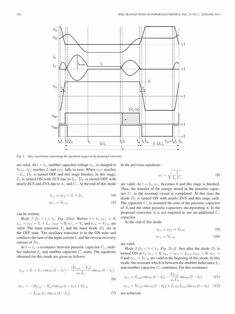
One switching cycle of the proposed novel ZVT-ZCT-PWMboost converter consist of eleven modes. In Fig. 2(a)–(k), theequivalent circuit diagrams of the operation modes are given re-spectively. The key waveforms concerning the operation modesare shown in Fig. 3. The detailed analysis of the proposed circuitis presented below.
Mode 1 [t0 < t < t1: Fig. 2(a)]: At the begining of this mode,the main transistor T1 and auxiliary transistor T2 are in the OFFstate. The main diode DF is in the ON state and the inputcurrent Ii flows through the main diode. At t = t0 , iT 1 = 0,iLs = iT 2 = 0, iDF = Ii, vC r = Vo and vC s = VC s0 are valid.The initial voltage of snubber capacitor VC s0 is constituted bythe efficiency of the resonant circuit. Soft-switching range ofthe circuit depends on the initial voltage of Cs . Soft switchingdepends on the value of VC s0 . The main diode DF is in theON state and conducts the input current Ii . At t = t0 , when theturn on signal is applied to the gate of the auxiliary transistorT2 , mode 1 begins. A resonance starts between snubber induc-
Fig. 2. Equivalent circuit schemes of the operation modes in the proposednovel ZVT-ZCT-PWM boost converter. (a) t0 < t < t1 . (b) t1 < t < t2 .(c) t2 < t < t3 . (d) t3 < t < t4 . (e) t4 < t < t5 . (f) t5 < t < t6 . (g) t6 <t < t7 . (h) t7 < t < t8 . (i) t8 < t < t9 . (j) t9 < t < t10 . (k) t10 < t <t11 = t0 .
tances Ls and snubber capacitor Cs . Due to the resonance T2current rises and DF current falls simultaneously. The rise rateof the current is limited because of the Ls snubber inductanceconnected serially to the auxiliary switch. So that the turn on ofthe auxiliary switch is provided with ZCS. For this interval, thefollowing equations can be written:
iLs = (Vo − VC s0)sin ωs(t − t0)
Lsωs(1)
vC s = Vo − (Vo − VC s0) cos ωs(t − t0). (2)
In these equations
ωs =√
1Ls Cs
(3)
258 IEEE TRANSACTIONS ON POWER ELECTRONICS, VOL. 29, NO. 1, JANUARY 2014
Fig. 3. Key waveforms concerning the operation stages in the proposed converter.
are valid. At t = t1 , snubber capacitor voltage vC s is charged toVC s1 , iT 2 reaches Ii and iDF falls to zero. When iDF reaches−Irr ,DF is turned OFF and this stage finishes. In this stage,T2 is turned ON with ZCS due to Ls . DF is turned OFF withnearly ZCS and ZVS due to Ls and Cr . At the end of this mode
iLs = iT 2 = Ii + Irr (4)
vC s = VC s1 (5)
can be written.Mode 2 [t1 < t < t2: Fig. 2(b)]: Before t = t1 , iT 1 = 0,
iLs = iT 2 = Ii + Irr , iDF = 0, vC r = Vo and vC s = VC s1 arevalid. The main transistor T1 and the main diode DF are inthe OFF state. The auxiliary transistor is in the ON state andconducts the sum of the input current Ii and the reverse recoverycurrent of DF .
At t = t1 , a resonance between parasitic capacitor Cr , snub-ber inductor Ls and snubber capacitor Cs starts. The equationsobtained for this mode are given as follows:
iLs = Ii + Irr cos ωr (t − t1) −(VC s1 − Vo)
ωrLssin ωr (t − t1)
(6)
vC r = −(VC s1 − Vo) cos ωr (t − t1) + VC s1
− LsωrIrr sinωr (t − t1). (7)
In the previous equations
ωr =√
1Ls Cr
(8)
are valid. At t = t2 , vC r becomes 0 and this stage is finished.Thus, the transfer of the energy stored in the parasitic capac-itor Cr to the resonant circuit is completed. At this time thediode D1 is turned ON with nearly ZVS and this stage ends.The capacitor Cr is assumed the sum of the parasitic capacitorof S1and the other parasitic capacitors incorporating it. In theproposed converter, it is not required to use an additional Cr
capacitor.At the end of this mode
iLs = iT 2 = ILs2 (9)
vC s = VC s2 (10)
are valid.Mode 3 [t2 < t < t3: Fig. 2(c)]: Just after the diode D1 is
turned ON at t2 , iT 1 = 0, iLs = iT 2 = ILs2 , iDF = 0, vC r =0 and vC s = VC s2 are valid at the begining of this mode. In thismode, the resonant which is between the snubber inductance Ls
and snubber capacitor Cs continues. For this resonance
iLs = ILs2 cos ωs(t − t2) −VC s1
ωsLssinωs(t − t2) (11)
vC s = VC s1 cos ωs(t − t2) + LsωsILs2 sin ωs(t − t2) (12)
are achieved.

ALTINTAS et al.: NOVEL ZVT-ZCT-PWM BOOST CONVERTER 259
At the beginning of this mode the voltage of Cr becomeszero, so that the diode D1 is turned ON and conducts the excessof snubber inductance Ls current from the input current. Theperiod of this stage is the ZVT duration of the main transistor sothat this interval is called ZVT duration. In this mode, controlsignal is applied to T1 while D1 is in the ON state in order toprovide ZVT turn ON of T1 . At t = t3 , this stage ends when thesnubber inductance Ls current falls to input current, and D1 isturned OFF under ZCS.
At the end of this mode
iLs = iT 2 = ILs3 = Ii (13)
vC s = VC s3 (14)
are valid.Mode 4 [t3 < t < t4: Fig. 2(d)]: This mode begins when the
diode D1 turns OFF. At the begining of this mode, iT 1 = 0,iLs = iT 2 = ILs3 = Ii, iDF = 0, vC r = 0, and vC s = VC s3 arevalid. The main transistor is turned ON with ZVT and its currentstarts to rise. The resonant between snubber inductance Ls andsnubber capacitor Cs continues. For this mode, the followingequations are derived:
iLs = Ii cos ωs(t − t3) −VC s4
ωsLssinωs(t − t3) (15)
vC s = VC s4 cos ωs(t − t3) + LsωsIi sin ωs(t − t3). (16)
At t = t4 , the main transistor current reaches to the input currentlevel and iLs becomes zero. The current through the auxiliarytransistor becomes zero and this mode ends by removing thecontrol signal of the auxiliary transistor.
At the end of this mode
iLs = iT 2 = ILs4 = 0 (17)
vC s = VC s4 (18)
are valid.Mode 5 [t4 < t < t5: Fig. 2(e)]: This mode begins when the
auxilary transistor T2 is perfectly turned OFF under ZCT. Forthis mode, iT 1 = Ii, iLs = iT 2 = ILs4 = 0, iDF = 0, vC r =0, and vC s = VC s4 are valid. In the beginning of this modethe diode D2 is turned ON with ZCS and its current starts torise. The resonant between snubber inductance Ls and snubbercapacitor Cs still continues. However, iLs becomes negative, sothe current through the main transistor is higher than the inputcurrent in this mode. The equations can be expressed as follows:
iLs = − VC s4
ωsLssin ωs(t − t4) (19)
vC s = VC s4 cos ωs(t − t4). (20)
At t = t5 , the main transistor current decrase to the input currentlevel and iLs becomes zero. iD2 becomes zero and it is turnedOFF under ZCS. At the end of this mode
iLs = iT 2 = ILs5 = 0 (21)
vC s = VC s5 (22)
are valid.
Mode 6 [t5 < t < t6: Fig. 2(f)]: At the begining of this mode,iT 1 = Ii, iLs = iT 2 = ILs4 = 0, iDF = 0, vC r = 0, and vC s =VC s5 are valid. In this mode, the main transistor continues toconduct the input current Ii and the snubber circuit is not active.This mode is the ON state of the conventional boost converter.The ON state duration is determined by the PWM control. Forthis mode
iT 1 = Ii (23)
can be written.Mode 7 [t6 < t < t7: Fig. 2(g)]: At the begining of this mode,
iT 1 = Ii, iLs = iT 2 = 0, iDF = 0, vC r = 0, and vC s = VC s5 arevalid. At t = t7 , when the control signal of the auxiliary transis-tor T2 is applied, a new resonance between snubber inductanceLs and snubber capacitor Cs starts through Cs–Ls–T2–T1 . Theequations can be expressed as follows:
iLs = − VC s5
ωsLssinωs(t − t5) (24)
vC s = VC s5 cos ωs(t − t5). (25)
Due to the snubber inductance Ls , the auxiliary transistor T2is turned ON with ZCS. The current which flows through thesnubber inductance rises and the main transistor current falls dueto the resonance, simultaneously. At t = t7 , when the curent ofT2 reaches to the input current level, the main transistor currentbecomes zero and this mode finishes. At the end of this mode
iLs = iT 2 = ILs7 = Ii (26)
vC s = VC s7 (27)
are valid.Mode 8 [t7 < t < t8: Fig. 2(h)]: At the begining of this mode,
iT 1 = 0, iLs = iT 2 = Ii, iDF = 0, vC r = 0, and vC s = VC s7are valid. This mode starts at t = t7 when T1 current falls tozero. D1 is turned ON with ZCS. If T1 is turned OFF when D1is ON, T1 turns OFF with ZVS and ZCS. The resonance startedbefore continues by through Cs–Ls–T2–D1 . D1 conducts theexcess of iLs from the input current. For this mode, the followingequations are derived:
iLs = Ii cos ωs(t − t8) −VC s7
ωsLssinωs(t − t8) (28)
vC s = VC s7 cos ωs(t − t8) + LsωsIi sin ωs(t − t8). (29)
Just before t = t8 , iD1 falls to zero. iD1 reaches −Irr at t = t8and turns OFF, and this stage ends. At the end of this mode
iLs = iT 2 = ILs8 = Ii − Irr (30)
vC s = VC s8 = VC s0 (31)
are valid.Mode 9 [t8 < t < t9: Fig. 2(i)]: This mode begins when
D1 is turned OFF under ZCS. For this mode, iT 1 = 0, iLs =iT 2 = ILs8 = Ii–Irr , iDF = 0, vC r = 0, and vC s = VC s8 =VC s0 are valid. A resonance between parasitic capacitor Cr ,snubber inductor Ls , and snubber capacitor Cs starts at t = t8 .At t = t9 , iLs falls to zero and the capacitor Cr is chargedfrom zero to VC s8 with this resonance. This mode ends by
260 IEEE TRANSACTIONS ON POWER ELECTRONICS, VOL. 29, NO. 1, JANUARY 2014
Fig. 4. Variation of IS 1m ax with Ls for different Cs values.
removing the control signal of the auxilary transistor T2 . Theauxilary transistor T2 is turned OFF with ZCS. For this mode,the following equations are derived:
iLs = Ii − Irr cos ωr (t − t8) −VC s8
ωrLssin ωr (t − t8) (32)
vC r = VC s8 − VC s8 cos ωr (t − t8) + LsωrIrr sinωr (t − t8).
(33)
At the end of this mode
iLs = iT 2 = ILs9 = 0 (34)
vC s = VC s9 = VC s0 (35)
are valid.Mode 10 [t9 < t < t10: Fig. 2(j)]: At t = t9 , iT 1 = 0, iLs =
iT 2 = ILs9 = 0, iDF = 0, vC r = VC s8 , and vC s = VC s9 =VC s0 are valid. During this mode, Cr is charged linearly underthe input current. For this mode
vCr= VC s9 +
Ii
Cr(t − t9) (36)
can be written. At instant t10 , when the voltage across the Cr
reaches output voltage Vo , the main diode DF is turned ON withZVS and this mode finishes.
Mode 11 [t10 < t < t11 = t0: Fig. 2(k)]: At t = t10 , iT 1 = 0,iLs = iT 2 = 0, iDF = 0, vC r = Vo , and vC s = VC s0 are valid.This mode is the OFF state of the conventional boost converter.During this mode, the main diode DF continues conductingthe input current Ii and the snubber circuit is not active. Theduration of this mode is determined by the PWM control. Forthis mode
iDF = Ii (37)
can be written.Therefore, at the moment t = t11 = t0 , one switching cycle
is completed and another switching cycle starts.
III. DESIGN PROCEDURE
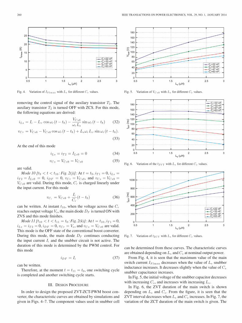
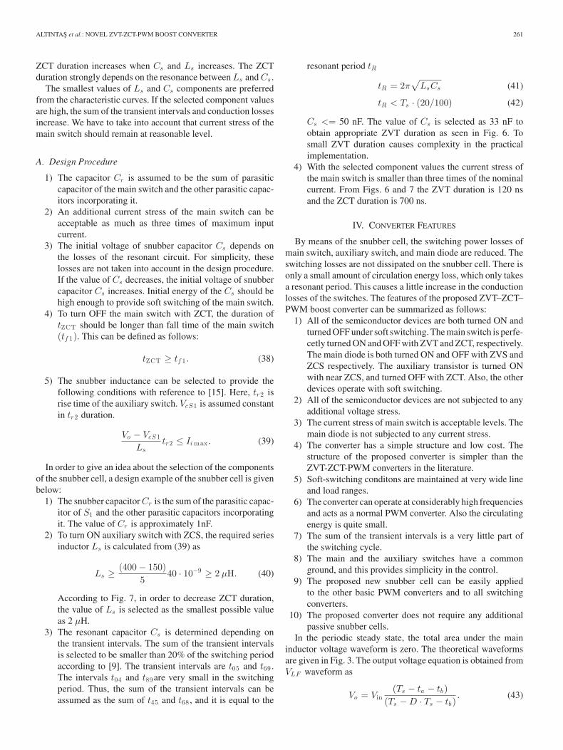
In order to design the proposed ZVT-ZCT-PWM boost con-verter, the characteristic curves are obtained by simulations andgiven in Figs. 4–7. The component values used in snubber cell
Fig. 5. Variation of VC s0 with Ls for different Cs values.
Fig. 6. Variation of the tZVT with Ls for different Cs values.
Fig. 7. Variation of tZCT with Ls for different Cs values.
can be determined from these curves. The characteristic curvesare obtained depending on Ls and Cs at nominal output power.
From Fig. 4, it is seen that the maximum value of the mainswitch current IS1max decreases when the value of Ls snubberinductance increases. It decreases slightly when the value of Cs
snubber capacitance increases.In Fig. 5, the initial voltage of the snubber capacitor decreases
with increasing Cs , and increases with increasing Ls .In Fig. 6, the ZVT duration of the main switch is shown
depending on Ls and Cs . From the figure, it is seen that theZVT interval decreases when Ls and Cs increases. In Fig. 7, thevariation of the ZCT duration of the main switch is given. The
ALTINTAS et al.: NOVEL ZVT-ZCT-PWM BOOST CONVERTER 261
ZCT duration increases when Cs and Ls increases. The ZCTduration strongly depends on the resonance between Ls and Cs .
The smallest values of Ls and Cs components are preferredfrom the characteristic curves. If the selected component valuesare high, the sum of the transient intervals and conduction lossesincrease. We have to take into account that current stress of themain switch should remain at reasonable level.
A. Design Procedure
1) The capacitor Cr is assumed to be the sum of parasiticcapacitor of the main switch and the other parasitic capac-itors incorporating it.
2) An additional current stress of the main switch can beacceptable as much as three times of maximum inputcurrent.
3) The initial voltage of snubber capacitor Cs depends onthe losses of the resonant circuit. For simplicity, theselosses are not taken into account in the design procedure.If the value of Cs decreases, the initial voltage of snubbercapacitor Cs increases. Initial energy of the Cs should behigh enough to provide soft switching of the main switch.
4) To turn OFF the main switch with ZCT, the duration oftZCT should be longer than fall time of the main switch(tf 1). This can be defined as follows:
tZCT ≥ tf 1 . (38)
5) The snubber inductance can be selected to provide thefollowing conditions with reference to [15]. Here, tr2 isrise time of the auxiliary switch. VcS1 is assumed constantin tr2 duration.
Vo − VcS1
Lstr2 ≤ Ii max . (39)
In order to give an idea about the selection of the componentsof the snubber cell, a design example of the snubber cell is givenbelow:
1) The snubber capacitor Cr is the sum of the parasitic capac-itor of S1 and the other parasitic capacitors incorporatingit. The value of Cr is approximately 1nF.
2) To turn ON auxiliary switch with ZCS, the required seriesinductor Ls is calculated from (39) as
Ls ≥ (400 − 150)5
40 · 10−9 ≥ 2 μH. (40)
According to Fig. 7, in order to decrease ZCT duration,the value of Ls is selected as the smallest possible valueas 2 μH.
3) The resonant capacitor Cs is determined depending onthe transient intervals. The sum of the transient intervalsis selected to be smaller than 20% of the switching periodaccording to [9]. The transient intervals are t05 and t69 .The intervals t04 and t89are very small in the switchingperiod. Thus, the sum of the transient intervals can beassumed as the sum of t45 and t68 , and it is equal to the
resonant period tR
tR = 2π√
LsCs (41)
tR < Ts · (20/100) (42)
Cs <= 50 nF. The value of Cs is selected as 33 nF toobtain appropriate ZVT duration as seen in Fig. 6. Tosmall ZVT duration causes complexity in the practicalimplementation.
4) With the selected component values the current stress ofthe main switch is smaller than three times of the nominalcurrent. From Figs. 6 and 7 the ZVT duration is 120 nsand the ZCT duration is 700 ns.
IV. CONVERTER FEATURES
By means of the snubber cell, the switching power losses ofmain switch, auxiliary switch, and main diode are reduced. Theswitching losses are not dissipated on the snubber cell. There isonly a small amount of circulation energy loss, which only takesa resonant period. This causes a little increase in the conductionlosses of the switches. The features of the proposed ZVT–ZCT–PWM boost converter can be summarized as follows:
1) All of the semiconductor devices are both turned ON andturned OFF under soft switching. The main switch is perfe-cetly turned ON and OFF with ZVT and ZCT, respectively.The main diode is both turned ON and OFF with ZVS andZCS respectively. The auxiliary transistor is turned ONwith near ZCS, and turned OFF with ZCT. Also, the otherdevices operate with soft switching.
2) All of the semiconductor devices are not subjected to anyadditional voltage stress.
3) The current stress of main switch is acceptable levels. Themain diode is not subjected to any current stress.
4) The converter has a simple structure and low cost. Thestructure of the proposed converter is simpler than theZVT-ZCT-PWM converters in the literature.
5) Soft-switching conditons are maintained at very wide lineand load ranges.
6) The converter can operate at considerably high frequenciesand acts as a normal PWM converter. Also the circulatingenergy is quite small.
7) The sum of the transient intervals is a very little part ofthe switching cycle.
8) The main and the auxiliary switches have a commonground, and this provides simplicity in the control.
9) The proposed new snubber cell can be easily appliedto the other basic PWM converters and to all switchingconverters.
10) The proposed converter does not require any additionalpassive snubber cells.
In the periodic steady state, the total area under the maininductor voltage waveform is zero. The theoretical waveformsare given in Fig. 3. The output voltage equation is obtained fromVLF waveform as
Vo = Vin(Ts − ta − tb)
(Ts − D · Ts − tb). (43)

262 IEEE TRANSACTIONS ON POWER ELECTRONICS, VOL. 29, NO. 1, JANUARY 2014
TABLE ISOFT-SWITCHING CAPABILITIES OF THE ZCT AND THE ZVT-ZCT CONVERTERS
In this equation, ta = t12 and tb = t8−10 . ta and tb are transientintervals in the proposed converter. In order to simplify theoutput voltage equation, the transient waveforms are assumedto be linear as shown in Fig. 3. The dependency of the outputvoltage to the load current increases as the load decreases.
The output voltage expression of the novel converter is thesame with the boost converter operating in continuous mode, ifthe transient intervals are neglected. The transient intervals aresmall compared with the switching period.
In order to evaluate the efficiency, the amount of losses shouldbe taken into account
η = Po/(Po + Ploss). (44)
The main losses in the converter are conduction (Pcond) andswitching losses (PSW ) of the semiconductor devices, and in-ductor losses
Ploss ∼= Pcond S1 + Psw S1 + Pcond S2 + Psw S2 + Pcond DF
+ Psw DF + Pinductor . (45)
In the proposed converter, switching losses are eliminated bymeans of soft switching. Inductor losses are very small and theycan be neglected. Thus, the losses can be approximated as
Ploss ∼= Pcond S1 + Pcond S2 + Pcond DF . (46)
In the proposed converter, there is a little increase in the con-duction losses as compared with the conventional hard switchedboost converter. Due to the elimination of the switching lossesthe efficiency is higher than the conventional one.
The soft-switching capabilities of the standard ZCT-PWMconverter and the proposed converter are compared in Table I.
In order to provide ZVT and ZCT for the main switch, theauxiliary circuits are operated twice in a switching period, bothat turn ON and turn OFF processes. In the turn ON processof the main switch, the energy of the parasitic capacitor Cr istransferred to the resonance circuit. The capacitor is discharged,body diode of the main switch turns ON, the main transistorturns ON with ZVT thus, no switching loss occurs in the turnON process.
V. EXPERIMENTAL RESULTS
A prototype of a 1 kW and 100 kHz boost converter shownin Fig. 8 was performed to verify the theoretical analysis of theproposed ZVT–ZCT PWM boost converter. The photograph re-lated to the experimental circuit is given in Fig. 9. The proposedconverter is established by adding the developed snubber cell tothe conventional boost converter.
Fig. 8. Experimental circuit of a 1 kW and 100 kHz ZVT-ZCT-PWM boostconverter.
Fig. 9. Experimental circuit.
TABLE IINOMINAL VALUES OF THE SEMICONDUCTOR DEVICES IN THE
PROPOSED CONVERTER
The LF main inductance is large enough to be considered asa constant current. Some nominal values of the semiconductordevices are listed in Table II with reference to the datasheets ofthe manufacturers.
The experimental results are shown in Fig. 10 at light load andin Fig. 11 at nominal load. In Figs. 10, 11(a) and (b), the controlsignals of the main and auxiliary switchs are shown. The controlsignal of the auxiliary switch is applied before about 150 ns andremoved after about 400 ns with regard to the turn ON signalof the main switch. Similarly, the control signal of the auxiliaryswitch is applied before about 300 ns with regard to the turn OFFsignal of the main switch. The signal of the auxiliary switch hasa constant width of 600 ns.
From the voltage, current, and control waveforms of the mainswitch S1 , given in Fig. 11(a), it can be seen that S1 is operatedunder soft switching at both turn ON and turn OFF processes.There is no overlap between voltage and current waveforms ofthe main switch. During the turn ON and turn OFF process ofthe main switch, its body diode is turned ON. Therefore, ZVTturn ON and ZCT turn OFF processes are perfectly realized forthe main switch. Also, from the waveforms it is seen that thereis no any additional voltage stress across the main switch andthe current stress is acceptable. Because of the current stress,the conduction loss of the main transistor increases slightly.
In Fig. 11(b), the voltage, current, and control waveforms ofthe auxiliary switch are shown. Auxiliary transistor is activated

ALTINTAS et al.: NOVEL ZVT-ZCT-PWM BOOST CONVERTER 263
Fig. 10. Experimental waveforms at light load (1μs/div). (a) vS 1 (200 V/div),iS 1 (5 A/div), and vG 1 (20 V/div). (b) vS 2 (200 V/div), iS 2 (5 A/div), and vG 2(20 V/div). (c) vD F (200 V/div) and iD F (5 A/div) (d) vo (200 V/div), vLs
(200 V/div), and vC s (200 V/div).
Fig. 11. Experimental waveforms at nominal load (1μs/div). (a) vS 1(200 V/div), iS 1 (10 A/div), and vG 1 (20 V/div). (b) vS 2 (200 V/div), iS 2(10 A/div), and vG 2 (20 V/div). (c) vD F (200 V/div) and iD F (10 A/div).(d) vo (200 V/div), vLs (200 V/div), and vC s (200 V/div).

264 IEEE TRANSACTIONS ON POWER ELECTRONICS, VOL. 29, NO. 1, JANUARY 2014
Fig. 12. Efficiency comparison of the proposed ZVT-ZCT converter, ZCTconverter, and PWM boost converter.
in both ZVT and ZCT processes of the main switch so it isswitched twice in a switching period. In the both operations, theconduction time of the auxiliary transistor is nearly 600 ns. Inthe ZVT and ZCT processes of the main switch, the auxiliaryswitch is turned ON under near ZCS and is turned OFF withZCT and near ZCS, respectively.
Because of the resonance circuit loss, the peak current throughthe auxiliary switch in the ZCT interval is lower than the ZVTinterval. As seen from the waveforms, there is no additionalvoltage stress across the auxiliary switch and it operates undersoft switching.
The ZVS turn ON and ZCS turn OFF processes of the maindiode are shown in Fig. 11(c). It can be seen that there is no anyadditional voltage and current stresses on the main diode. Thewaveforms of the output voltage, resonant inductance voltage,and resonant capacitor voltage are shown in Fig. 11(d). It can beseen that, the voltage across Cs is returned to initial value at theend of one switching period. From the experimental results, itis also observed that the soft-switching conditions of the novelconverter are maintained for the overall load ranges.
From Fig. 12 it can be seen that the efficiency values of thenovel converter are much higher than that of the hard switchingconverter. Also, there are important differences between theproposed ZVT–ZCT–PWM converter and the standard ZCT–PWM converter. These are listed in Table I. When the proposedconverter is operated as ZCT–PWM converter the efficiencydecreases due to the turn ON switching losses of the main IGBT.At 100 kHz operation frequency and at nominal load, the turnON switching loss of the main IGBT is around 10 W. Besidesthat, the auxiliary switch and the main diode turns OFF underhard switching. Thus, the efficiency of the ZCT converter islower than the proposed ZVT-ZCT-PWM converter.
The overall efficiency of the proposed converter is measuredabout 97.8% at the nominal output power. As a result, it can beclearly seen that the predicted theoretical analysis and operationprinciples of the novel ZVT–ZCT–PWM boost converter areexperimentally verified.
VI. CONCLUSION
In this study, a PWM boost converter with a novel activesnubber cell has been analyzed in detail. This active snubbercell provides ZVT turn on and ZCT turn OFF together for themain switch of the converter. Also, the proposed snubber cell isimplemented by using only one quasi-resonant circuit withoutan important increase in cost and complexity.
In the proposed converter, all semiconductor devices areswitched under soft switching. In the ZVT and ZCT processes,the auxiliary switch is turned ON under ZCS and is turned OFFwith ZCT and near ZCS, respectively. There is no additionalvoltage stress across the main and auxiliary switches.The maindiode is not subjected to any additional voltage and currentstresses. The operation principles and steady-state analysis ofthe proposed converter are presented. In order to verify the the-oretical analysis, a prototype of the proposed circuit is realizedin the laboratory. The novel ZVT-ZCT-PWM boost converterusing the proposed snubber cell has desired features of the ZVTand ZCT converters. It is observed that the operation principlesand the theoretical analysis of the novel converter are exactlyverified by experimental results taken from the converter op-erating at 1 kW and 100 kHz. Additionally, at nominal outputpower, the converter efficiency reaches approximately to 97.8%.
REFERENCES
[1] G. Hua, C. S. Leu, Y. Jiang, and F. C. Lee, “Novel zero-voltage-transitionPWM converters,” IEEE Trans. Power Electron., vol. 9, no. 2, pp. 213–219, Mar. 1994.
[2] G. Hua, E. X. Yang, Y. Jiang, and F. C. Lee, “Novel zero-current-transitionPWM converters,” IEEE Trans. Power Electron., vol. 9, pp. 601–606, Nov.1994.
[3] H. Mao, F. C. Lee, X. Zhou, H. Dai, M. Cosan, and D. Boroyevich, “Im-proved zero-current-transition converters for high-power applications,”IEEE Trans. Ind. Appl., vol. 33, no. 5, pp. 1220–1232, Sep./Oct. 1997.
[4] J. G. Cho, J. W. Baek, G. H. Rim, and I. Kang, “Novel zero-voltage-transition PWM multiphase converters,” IEEE Trans. Power Electron.,vol. 13, no. 1, pp. 152–159, Jan. 1998.
[5] C. J. Tseng and C. L. Chen, “Novel ZVT-PWM converters with activesnubbers,” IEEE Trans. Power Electron., vol. 13, no. 5, pp. 861–869, Sep.1998.
[6] V. Grigore and J. Kyyra, “A new zero-voltage-transition PWM buck con-verter,” in Proc. 9th Mediterr. Electrotech. Conf., Tel Aviv, Israel, 1998,vol. 2, pp. 1241–1245.
[7] J. M. P. Menegaz, M. A. Co., D. S. L. Simonetti, and L. F. Vieira, “Im-proving the operation of ZVT DC-DC Converters,” in Proc. 30th PowerElectron. Spec. Conf., 1999, vol. 1, pp. 293–297.
[8] K. M. Smith and K. M. Smedley, “Properties and synthesis of passivelossless soft-switching PWM converters,” IEEE Trans. Power Electron.,vol. 14, no. 5, pp. 890–899, Sep. 1999.
[9] C. M. de O. Stein and H. L. Hey, “A true ZCZVT commutation cell forPWM converters,” IEEE Trans. Power Electron., vol. 15, no. 1, pp. 185–193, Jan. 2000.
[10] D. Y. Lee, B. K. Lee, S. B. Yoo, and D. S. Hyun, “An improved full-bridge zero-voltage-transition PWM DC/DC converter with zero-voltage/ zero-current switching of the auxiliary switches,” IEEE Trans. Ind. Appl.,vol. 36, no. 2, pp. 558–566, Mar./Apr. 2000.
[11] T. W. Kim, H. S. Kim, and H. W. Ahn, “An improved ZVT PWM boostconverter,” in Proc. 31th Power Electron. Spec. Conf., vol. 2, Galway,Ireland, 2000, pp. 615–619.
[12] H. Bodur and A. F. Bakan, “A new ZVT-PWM DC-DC converter,” IEEETrans. Power Electron., vol. 17, no. 1, pp. 40–47, Jan. 2002.
[13] H. Yu, B. M. Song, and J. S. Lai, “Design of a novel ZVT soft-switchingchopper,” IEEE Trans. Power Electron., vol. 17, no. 1, pp. 101–108, Jan.2002.

ALTINTAS et al.: NOVEL ZVT-ZCT-PWM BOOST CONVERTER 265
[14] D. Y. Lee, M. K. Lee, D. S. Hyun, and I. Choy, “New zero-current-transition PWM DC/DC converters without current stres,” IEEE Trans.Power Electron., vol. 18, no. 1, pp. 95–104, Jan. 2003.
[15] H. Bodur and A. F. Bakan, “A new ZVT-ZCT-PWM DC-DC converter,”IEEE Trans. Power Electron., vol. 19, no. 3, pp. 676–684, May 2004.
[16] A. F. Bakan, H. Bodur, and I. Aksoy, “A novel ZVT-ZCT PWM DC-DCconverter,” in Proc. 11th Eur. Conf. Power Electron. Appl., Sep. 2005,pp. 1–8.
[17] C. M. Wang, “Novel zero-voltage-transition PWM DC-DC converters,”IEEE Trans. Ind. Electron., vol. 53, no. 1, pp. 254–262, Feb. 2006.
[18] W. Huang and G. Moschopoulos, “A new family of zero-voltage-transitionPWM converters with dual active auxiliary circuits,” IEEE Trans. PowerElectron., vol. 21, no. 2, pp. 370–379, Mar. 2006.
[19] P. Das and G. Moschopoulos, “A comparative study of zero-current-transition PWM converters,” IEEE Trans. Ind. Electron., vol. 54, no. 3,pp. 1319–1328, Jun. 2007.
[20] H. Wannian, G. Xing, S. Bassan, and G. Moschopoulos, “Novel dualauxiliary circuits for ZVT-PWM converters,” Can. J. Electr. Comput.Eng., vol. 33, pp. 153–160, Summer-Fall 2008.
[21] I. Aksoy, H. Bodur, and A. F. Bakan, “A new ZVT-ZCT-PWM DC–DCconverter,” IEEE Trans. Power Electron., vol. 25, no. 8, pp. 2093–2105,Aug. 2010.
[22] E. Adib and H. Farzanehfard, “Family of zero-voltage transition pulsewidth modulation converters with low auxiliary switch voltage stress,”IET Power Electron., vol. 4, pp. 447–453, Apr. 2011.
[23] W. Li, Y. Zhao, Y. Deng, and X. He, “Interleaved converter with voltagemultiplier cell for high step-up and high-efficiency conversion,” IEEETrans. Power Electron., vol. 25, no. 9, pp. 2397–2408, Sep. 2010.
[24] Y. Zhao, W. Li, Y. Deng, and X. He, “Analysis, design, and experimen-tation of an isolated ZVT boost converter with coupled inductors,” IEEETrans. Power Electron., vol. 26, no. 2, pp. 541–550, Feb. 2011.
[25] W. Li, W. Li, and X. He, “Zero-voltage transition interleaved high step-upconverter with built-in transformer,” IET Power Electron., vol. 4, pp. 523–531, May 2011.
[26] W. Li, Y. Zhao, J. Wu, and X. He, “Interleaved high step-up converterwith winding-cross-coupled inductors and voltage multiplier cells,” IEEETrans. Power Electron., vol. 27, no. 1, pp. 133–143, Jan. 2012.
Nihan Altintas was born in Balıkesir, Turkey, in1980. She received the B.S. and M.S. degrees in elec-trical engineering from Yildiz Technical University,Yildiz, Turkey, in 2004 and 2007, respectively, whereshe is working toward the Ph.D. degree in electricalengineering.
She is also a Research Assistant in the Departmentof Electrical Engineering at Yildiz Technical Univer-sity. She was also employed in two research projectsconcerning power electronics. Her research interestincludes dc–dc converters, welding machines, and
soft-switching techniques in power electronics.
A. Faruk Bakan was born in Istanbul, Turkey, in1972. He received the B.S. degree in electronics andcommunication engineering, the M.S. degree in elec-trical engineering, and the Ph.D. degree in electricalengineering from Yildiz Technical University, Yildiz,Turkey, in 1994, 1997, and 2002, respectively.
Since 2002, he has been working as an Assis-tant Professor in the Department of Electrical En-gineering, Yildiz Technical University. He has pub-lished 20 journal and conference papers in the areaof power electronics. He was also employed in seven
research projects concerning power electronics.His research interests include di-rect torque control, photovoltaic inverters, welding machines, and soft-switchingtechniques in power electronics.
Ismail Aksoy was born in Cologne, Germany, in1977. He received the B.S., M.S., and Ph.D. de-grees in electrical engineering from Yildiz TechnicalUniversity, Yildiz, Turkey, in 1999, 2001, and 2007,respectively.
He was a Research Assistant from 1999 to 2008in the Department of Electrical Engineering, YildizTechnical University. Since 2008 he has been work-ing as an Assistant Professor in the Department ofElectrical Engineering, Yildiz Technical University.He has published more than 15 journal and confer-
ence papers in the area of power electronics. He was also employed in threeresearch projects concerning power electronics. His research interests includepower factor correction, switching power supplies, high-frequency power con-version, and active and passive snubber cells in power electronics.